KR20140144963A - Display device - Google Patents
Display device Download PDFInfo
- Publication number
- KR20140144963A KR20140144963A KR1020130067235A KR20130067235A KR20140144963A KR 20140144963 A KR20140144963 A KR 20140144963A KR 1020130067235 A KR1020130067235 A KR 1020130067235A KR 20130067235 A KR20130067235 A KR 20130067235A KR 20140144963 A KR20140144963 A KR 20140144963A
- Authority
- KR
- South Korea
- Prior art keywords
- connection terminal
- display
- circuit board
- substrate
- disposed
- Prior art date
Links
Images


Classifications
-
- H—ELECTRICITY
- H10—SEMICONDUCTOR DEVICES; ELECTRIC SOLID-STATE DEVICES NOT OTHERWISE PROVIDED FOR
- H10K—ORGANIC ELECTRIC SOLID-STATE DEVICES
- H10K59/00—Integrated devices, or assemblies of multiple devices, comprising at least one organic light-emitting element covered by group H10K50/00
- H10K59/10—OLED displays
- H10K59/12—Active-matrix OLED [AMOLED] displays
- H10K59/131—Interconnections, e.g. wiring lines or terminals
-
- H—ELECTRICITY
- H10—SEMICONDUCTOR DEVICES; ELECTRIC SOLID-STATE DEVICES NOT OTHERWISE PROVIDED FOR
- H10K—ORGANIC ELECTRIC SOLID-STATE DEVICES
- H10K59/00—Integrated devices, or assemblies of multiple devices, comprising at least one organic light-emitting element covered by group H10K50/00
- H10K59/10—OLED displays
-
- G—PHYSICS
- G09—EDUCATION; CRYPTOGRAPHY; DISPLAY; ADVERTISING; SEALS
- G09F—DISPLAYING; ADVERTISING; SIGNS; LABELS OR NAME-PLATES; SEALS
- G09F9/00—Indicating arrangements for variable information in which the information is built-up on a support by selection or combination of individual elements
- G09F9/30—Indicating arrangements for variable information in which the information is built-up on a support by selection or combination of individual elements in which the desired character or characters are formed by combining individual elements
- G09F9/301—Indicating arrangements for variable information in which the information is built-up on a support by selection or combination of individual elements in which the desired character or characters are formed by combining individual elements flexible foldable or roll-able electronic displays, e.g. thin LCD, OLED
-
- G—PHYSICS
- G09—EDUCATION; CRYPTOGRAPHY; DISPLAY; ADVERTISING; SEALS
- G09G—ARRANGEMENTS OR CIRCUITS FOR CONTROL OF INDICATING DEVICES USING STATIC MEANS TO PRESENT VARIABLE INFORMATION
- G09G3/00—Control arrangements or circuits, of interest only in connection with visual indicators other than cathode-ray tubes
- G09G3/20—Control arrangements or circuits, of interest only in connection with visual indicators other than cathode-ray tubes for presentation of an assembly of a number of characters, e.g. a page, by composing the assembly by combination of individual elements arranged in a matrix no fixed position being assigned to or needed to be assigned to the individual characters or partial characters
- G09G3/22—Control arrangements or circuits, of interest only in connection with visual indicators other than cathode-ray tubes for presentation of an assembly of a number of characters, e.g. a page, by composing the assembly by combination of individual elements arranged in a matrix no fixed position being assigned to or needed to be assigned to the individual characters or partial characters using controlled light sources
- G09G3/30—Control arrangements or circuits, of interest only in connection with visual indicators other than cathode-ray tubes for presentation of an assembly of a number of characters, e.g. a page, by composing the assembly by combination of individual elements arranged in a matrix no fixed position being assigned to or needed to be assigned to the individual characters or partial characters using controlled light sources using electroluminescent panels
- G09G3/32—Control arrangements or circuits, of interest only in connection with visual indicators other than cathode-ray tubes for presentation of an assembly of a number of characters, e.g. a page, by composing the assembly by combination of individual elements arranged in a matrix no fixed position being assigned to or needed to be assigned to the individual characters or partial characters using controlled light sources using electroluminescent panels semiconductive, e.g. using light-emitting diodes [LED]
- G09G3/3208—Control arrangements or circuits, of interest only in connection with visual indicators other than cathode-ray tubes for presentation of an assembly of a number of characters, e.g. a page, by composing the assembly by combination of individual elements arranged in a matrix no fixed position being assigned to or needed to be assigned to the individual characters or partial characters using controlled light sources using electroluminescent panels semiconductive, e.g. using light-emitting diodes [LED] organic, e.g. using organic light-emitting diodes [OLED]
-
- H—ELECTRICITY
- H05—ELECTRIC TECHNIQUES NOT OTHERWISE PROVIDED FOR
- H05B—ELECTRIC HEATING; ELECTRIC LIGHT SOURCES NOT OTHERWISE PROVIDED FOR; CIRCUIT ARRANGEMENTS FOR ELECTRIC LIGHT SOURCES, IN GENERAL
- H05B33/00—Electroluminescent light sources
- H05B33/02—Details
- H05B33/04—Sealing arrangements, e.g. against humidity
-
- H—ELECTRICITY
- H05—ELECTRIC TECHNIQUES NOT OTHERWISE PROVIDED FOR
- H05B—ELECTRIC HEATING; ELECTRIC LIGHT SOURCES NOT OTHERWISE PROVIDED FOR; CIRCUIT ARRANGEMENTS FOR ELECTRIC LIGHT SOURCES, IN GENERAL
- H05B33/00—Electroluminescent light sources
- H05B33/10—Apparatus or processes specially adapted to the manufacture of electroluminescent light sources
-
- H—ELECTRICITY
- H10—SEMICONDUCTOR DEVICES; ELECTRIC SOLID-STATE DEVICES NOT OTHERWISE PROVIDED FOR
- H10K—ORGANIC ELECTRIC SOLID-STATE DEVICES
- H10K50/00—Organic light-emitting devices
- H10K50/80—Constructional details
- H10K50/84—Passivation; Containers; Encapsulations
-
- H—ELECTRICITY
- H10—SEMICONDUCTOR DEVICES; ELECTRIC SOLID-STATE DEVICES NOT OTHERWISE PROVIDED FOR
- H10K—ORGANIC ELECTRIC SOLID-STATE DEVICES
- H10K50/00—Organic light-emitting devices
- H10K50/80—Constructional details
- H10K50/84—Passivation; Containers; Encapsulations
- H10K50/846—Passivation; Containers; Encapsulations comprising getter material or desiccants
-
- H—ELECTRICITY
- H10—SEMICONDUCTOR DEVICES; ELECTRIC SOLID-STATE DEVICES NOT OTHERWISE PROVIDED FOR
- H10K—ORGANIC ELECTRIC SOLID-STATE DEVICES
- H10K59/00—Integrated devices, or assemblies of multiple devices, comprising at least one organic light-emitting element covered by group H10K50/00
- H10K59/10—OLED displays
- H10K59/12—Active-matrix OLED [AMOLED] displays
- H10K59/1201—Manufacture or treatment
-
- H—ELECTRICITY
- H10—SEMICONDUCTOR DEVICES; ELECTRIC SOLID-STATE DEVICES NOT OTHERWISE PROVIDED FOR
- H10K—ORGANIC ELECTRIC SOLID-STATE DEVICES
- H10K71/00—Manufacture or treatment specially adapted for the organic devices covered by this subclass
-
- H—ELECTRICITY
- H10—SEMICONDUCTOR DEVICES; ELECTRIC SOLID-STATE DEVICES NOT OTHERWISE PROVIDED FOR
- H10K—ORGANIC ELECTRIC SOLID-STATE DEVICES
- H10K71/00—Manufacture or treatment specially adapted for the organic devices covered by this subclass
- H10K71/851—Division of substrate
Landscapes
- Engineering & Computer Science (AREA)
- Physics & Mathematics (AREA)
- Manufacturing & Machinery (AREA)
- Microelectronics & Electronic Packaging (AREA)
- General Physics & Mathematics (AREA)
- Theoretical Computer Science (AREA)
- Optics & Photonics (AREA)
- Computer Hardware Design (AREA)
- Electroluminescent Light Sources (AREA)
- Devices For Indicating Variable Information By Combining Individual Elements (AREA)
Abstract
Description
본 발명은 표시 장치에 관한 것이다. The present invention relates to a display device.
최근 모니터 또는 텔레비전 등의 경량화 및 박형화가 요구되고 있으며, 이러한 요구에 따라 음극선관(cathode ray tube, CRT)이 액정 표시 장치(liquid crystal display, LCD)로 대체되고 있다. 그러나, 액정 표시 장치는 수동 발광 소자로서 별도의 백라이트(backlight)가 필요할 뿐만 아니라, 응답 속도 및 시야각 등에서 많은 문제점이 있다. 최근 이러한 문제점을 극복할 수 있는 표시 장치로서, 유기 발광 표시 장치(organic light emitting diode display, OLED display)가 주목받고 있다. 유기 발광 표시 장치의 단위 표시 소자들은 구동 회로에 의해 제어된다. 구동 회로는 테입 캐리어 패키지(tape carrier package) 방법으로 장착될 수 있다. 그러나, 테입 캐리어 패키지가 접힌 상태로 장착이 되어 불량이 발생하기 쉽다. 2. Description of the Related Art In recent years, a cathode ray tube (CRT) has been replaced by a liquid crystal display (LCD) in accordance with such a demand. However, the liquid crystal display device requires a separate backlight as a passive light emitting element, and has many problems in terms of response speed and viewing angle. Recently, organic light emitting diode (OLED) displays have been attracting attention as display devices capable of overcoming such problems. The unit display elements of the organic light emitting display are controlled by a driving circuit. The driving circuit can be mounted by a tape carrier package method. However, the tape carrier package is mounted in a folded state, and defects tend to occur.
본 발명이 해결하고자 하는 과제는 신뢰성이 향상된 표시 장치를 제공하는데 있다.A problem to be solved by the present invention is to provide a display device with improved reliability.
상기 과제를 해결하기 위한 본 발명에 따른 표시 장치는, 표시 영역과 비표시 영역을 포함하는 표시 기판; 상기 표시 영역에서 상기 표시 기판 상에 배치되는 복수개의 단위 표시 소자들; 상기 비표시 영역에서 상기 표시 기판 상에 배치되며 상기 단위 표시 소자와 전기적으로 연결되는 제 1 접속 단자; 상기 비표시 영역에서 상기 표시 기판 상에 배치되는 회로 기판; 및 상기 비표시 영역에서 상기 표시 기판 상에 배치되며 상기 회로 기판과 상기 기 제 1 접속 단자를 전기적으로 연결시키는 반도체 패키지를 포함하되, 상기 반도체 패키지는 평평하다.According to an aspect of the present invention, there is provided a display device including: a display substrate including a display region and a non-display region; A plurality of unit display elements disposed on the display substrate in the display area; A first connection terminal disposed on the display substrate in the non-display region and electrically connected to the unit display element; A circuit board disposed on the display substrate in the non-display area; And a semiconductor package disposed on the display substrate in the non-display area and electrically connecting the circuit board and the first connection terminal, wherein the semiconductor package is flat.
상기 패키지 기판은 하부면에 배치되는 제 2 접속 단자, 상부면에 배치되며 서로 이격되는 제 3 접속 단자와 제 4 접속 단자, 및 상기 패키지 기판을 관통하여 상기 제 2 접속 단자와 상기 제 3 접속 단자를 전기적으로 연결시키는 관통 비아를 더 포함할 수 있으며, 상기 제 1 접속 단자는 상기 제 2 접속 단자와 전기적으로 연결되고 상기 회로 기판은 상기 제 4 접속 단자와 전기적으로 연결될 수 있다. Wherein the package substrate has a second connection terminal disposed on a lower surface thereof, a third connection terminal and a fourth connection terminal disposed on the upper surface and spaced apart from each other, and a second connection terminal through the package substrate, The first connection terminal may be electrically connected to the second connection terminal, and the circuit board may be electrically connected to the fourth connection terminal.
상기 표시 장치는 상기 제 1 접속 단자와 상기 제 2 접속 단자 사이에 개재되어 이들을 전기적으로 연결시키는 제 1 연결 부재를 더 포함할 수 있으며, 상기 제 1 연결 부재는 이방성 전도성 필름 또는 솔더볼일 수 있다.The display device may further include a first connection member interposed between the first connection terminal and the second connection terminal to electrically connect the first connection terminal and the second connection terminal, wherein the first connection member may be an anisotropic conductive film or a solder ball.
상기 패키지 기판은 단단하거나 유연할 수 있다.The package substrate may be rigid or flexible.
상기 표시 장치는 상기 패키지 기판 상에 실장되며 상기 제 3 및 제 4 접속 단자들과 접하는 반도체 칩을 더 포함할 수 있으며, 상기 반도체 칩의 하부면은 상기 표시 기판의 상부면에 대하여 평행할 수 있다.The display device may further include a semiconductor chip mounted on the package substrate and in contact with the third and fourth connection terminals, and the lower surface of the semiconductor chip may be parallel to the upper surface of the display substrate .
일 예에 있어서, 상기 회로 기판의 일부분 아래에 상기 패키지 기판이 배치될 수 있으며, 상기 표시 장치는, 상기 회로 기판과 상기 표시 기판 사이에 배치되어 상기 회로 기판을 지지하는 브래킷을 더 포함할 수 있다. 이때, 상기 회로 기판은 하부면에 배치되는 제 5 접속 단자를 더 포함할 수 있으며, 상기 표시 장치는, 상기 제 5 접속 단자와 상기 제 4 접속 단자 사이에 개재되며 이들을 전기적으로 연결시키는 제 2 연결 부재를 더 포함할 수 있다. 상기 제 2 연결 부재는 이방성 전도성 필름 또는 솔더볼일 수 있다.In one example, the package substrate may be disposed under a portion of the circuit board, and the display device may further include a bracket disposed between the circuit board and the display board to support the circuit board . The circuit board may further include a fifth connection terminal disposed on a lower surface of the circuit board, and the display device may include a second connection interposed between the fifth connection terminal and the fourth connection terminal and electrically connecting the fifth connection terminal and the fourth connection terminal, Member. ≪ / RTI > The second connecting member may be an anisotropic conductive film or a solder ball.
다른 예에 있어서, 상기 회로 기판은 상기 표시 기판 상에 부착될 수 있다. 이때, 상기 회로 기판은 상부면에 배치되는 제 5 접속 단자를 더 포함할 수 있으며, 상기 표시 장치는 상기 제 5 접속 단자와 상기 제 4 접속 단자를 전기적으로 연결시키는 제 3 연결 부재를 더 포함할 수 있다. 상기 제 3 연결 부재는 와이어일 수 있다. In another example, the circuit board may be attached to the display substrate. The circuit board may further include a fifth connection terminal disposed on an upper surface of the circuit board, and the display device further includes a third connection member electrically connecting the fifth connection terminal and the fourth connection terminal . The third connecting member may be a wire.
상기 표시 장치는, 상기 표시 기판, 상기 회로 기판 및 상기 반도체 패키지를 감싸는 프레임을 더 포함할 수 있으며, 상기 프레임은 상기 표시 영역과 중첩되는 개구부를 포함한다.The display device may further include a frame surrounding the display substrate, the circuit substrate, and the semiconductor package, and the frame includes an opening overlapped with the display area.
상기 단위 표시 소자는 단위 스위치 소자와 이에 연결된 단위 발광 소자를 포함한다.The unit display element includes a unit switch element and a unit light emitting element connected to the unit switch element.
상기 표시 장치는 유기 발광 표시 장치일 수 있다.The display device may be an organic light emitting display device.
상기 패키지 기판의 모든 가장자리들은 같은 높이에 위치할 수 있다.All the edges of the package substrate may be located at the same height.
본 발명의 일 예에 따른 표시 장치에 포함되어 단위 표시 소자들을 구동하는 전기적 신호를 제공하는 반도체 패키지는 접히지 않고 반도체 패키지는 평평한 상태를 가지므로 불량 발생을 줄일 수 있다. 이로써 신뢰성이 향상된 표시 장치를 제공할 수 있다. 또한, 반도체 패키지가 표시 기판의 측면쪽으로 접히지 않으므로 비표시 영역의 면적을 줄일 수 있다. 이로써 동일한 화면 크기 대비 전체 사이즈를 줄일 수 있다. The semiconductor package included in the display device according to an exemplary embodiment of the present invention to provide an electrical signal for driving the unit display elements is not folded, and the semiconductor package has a flat state, thereby reducing the occurrence of defects. Thus, a display device with improved reliability can be provided. Further, since the semiconductor package is not folded toward the side of the display substrate, the area of the non-display area can be reduced. This reduces the overall size compared to the same screen size.
도 1은 본 발명의 일 예에 따른 표시 장치의 단면도이다.
도 2 내지 5는 도 1의 표시 장치를 제조하는 과정들을 나타내는 단면도들이다.
도 6 및 7은 본 발명의 다른 예들에 따른 표시 장치의 레이아웃들이다.
도 8 내지 도 11은 본 발명의 예들에 따른 표시 장치가 적용된 멀티미디어 장치의 예들을 보여준다. 1 is a cross-sectional view of a display device according to an example of the present invention.
Figs. 2 to 5 are cross-sectional views showing the processes of manufacturing the display device of Fig.
6 and 7 are layouts of a display device according to other examples of the present invention.
8 to 11 show examples of a multimedia device to which a display device according to the exemplary embodiments of the present invention is applied.
본 발명의 구성 및 효과를 충분히 이해하기 위하여, 첨부한 도면을 참조하여 본 발명의 바람직한 실시예들을 설명한다. 그러나 본 발명은 이하에서 개시되는 실시예들에 한정되는 것이 아니라, 여러가지 형태로 구현될 수 있고 다양한 변경을 가할 수 있다. 단지, 본 실시예들에 대한 설명은 본 발명의 개시가 완전하도록 하며, 본 발명이 속하는 기술 분야의 통상의 지식을 가진 자에게 발명의 범주를 완전하게 알려주기 위하여 제공되는 것이다. 첨부된 도면에서 구성 요소들은 설명의 편의를 위하여 그 크기가 실제보다 확대하여 도시한 것이며, 각 구성 요소의 비율은 과장되거나 축소될 수 있다. 도면상의 동일한 구성 요소에 대해서는 동일한 참조부호 또는 용어를 사용하고, 동일한 구성 요소에 대해서 중복된 설명은 생략될 수 있다. In order to fully understand the structure and effects of the present invention, preferred embodiments of the present invention will be described with reference to the accompanying drawings. However, the present invention is not limited to the embodiments described below, but may be embodied in various forms and various modifications may be made. It should be understood, however, that the description of the embodiments is provided to enable the disclosure of the invention to be complete, and will fully convey the scope of the invention to those skilled in the art. In the accompanying drawings, the constituent elements are shown enlarged for the sake of convenience of explanation, and the proportions of the constituent elements may be exaggerated or reduced. The same reference numerals or terms are used for the same constituent elements in the drawings, and redundant explanations for the same constituent elements can be omitted.
어떤 구성 요소가 다른 구성 요소에 "상에" 있다거나 "연결되어" 있다고 기재된 경우, 다른 구성 요소에 상에 직접 맞닿아 있거나 또는 연결되어 있을 수 있지만, 중간에 또 다른 구성 요소가 존재할 수 있다고 이해되어야 할 것이다. 반면, 어떤 구성 요소가 다른 구성 요소의 "바로 위에" 있다거나 "직접 연결되어" 있다고 기재된 경우에는, 중간에 또 다른 구성 요소가 존재하지 않는 것으로 이해될 수 있다. 구성 요소들 간의 관계를 설명하는 다른 표현들, 예를 들면, "~사이에"와 "직접 ~사이에" 등도 마찬가지로 해석될 수 있다. It is to be understood that when an element is described as being "on" or "connected to" another element, it may be directly in contact with or coupled to another element, but there may be another element in between . On the other hand, when an element is described as being "directly on" or "directly connected" to another element, it can be understood that there is no other element in between. Other expressions that describe the relationship between components, for example, "between" and "directly between"
제 1, 제 2 등의 용어는 다양한 구성요소들을 설명하는데 사용될 수 있지만, 상기 구성요소들은 상기 용어들에 의해 한정되어서는 안된다. 상기 용어들은 하나의 구성요소를 다른 구성요소로부터 구별하는 목적으로만 사용될 수 있다. 예를 들어, 본 발명의 권리 범위를 벗어나지 않으면서 제 1 구성요소는 제 2 구성요소로 명명될 수 있고, 유사하게 제 2 구성요소도 제 1 구성요소로 명명될 수 있다. The terms first, second, etc. may be used to describe various elements, but the elements should not be limited by the terms. The terms may only be used for the purpose of distinguishing one element from another. For example, without departing from the scope of the present invention, the first component may be referred to as a second component, and similarly, the second component may also be referred to as a first component.
단수의 표현은 문맥상 명백하게 다르게 표현하지 않는 한, 복수의 표현을 포함한다. "포함한다" 또는 "가진다" 등의 용어는 명세서 상에 기재된 특징, 숫자, 단계, 동작, 구성요소, 부분품 또는 이들을 조합한 것이 존재함을 지정하기 위한 것으로, 하나 또는 그 이상의 다른 특징들이나 숫자, 단계, 동작, 구성요소, 부분품 또는 이들을 조합한 것들이 부가될 수 있는 것으로 해석될 수 있다. The singular forms "a", "an" and "the" include plural referents unless the context clearly dictates otherwise. The word "comprising" or "having ", when used in this specification, is intended to specify the presence of stated features, integers, steps, operations, elements, A step, an operation, an element, a part, or a combination thereof.
본 발명의 실시예들에서 사용되는 용어들은 다르게 정의되지 않는 한, 해당 기술 분야에서 통상의 지식을 가진 자에게 통상적으로 알려진 의미로 해석될 수 있다.The terms used in the embodiments of the present invention may be construed as commonly known to those skilled in the art unless otherwise defined.
이하, 첨부한 도면을 참조하여 본 발명의 바람직한 실시 예를 설명함으로써 본 발명을 상세히 설명한다. 각 도면에 제시된 동일한 참조부호는 동일한 부재를 나타낸다. Hereinafter, the present invention will be described in detail with reference to the preferred embodiments of the present invention with reference to the accompanying drawings. Like reference symbols in the drawings denote like elements.
도 1은 본 발명의 일 예에 따른 표시 장치의 단면도이다.1 is a cross-sectional view of a display device according to an example of the present invention.
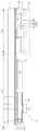
도 1을 참조하면, 본 예에 따른 표시 장치(100)는 유기 발광 표시 장치일 수 있다. 상기 표시 장치(100)는 표시 기판(1)을 포함한다. 상기 표시 기판(1)은 투명한 물질로 예를 들면 유리 등으로 형성될 수 있다. 상기 표시 기판(1)은 입력된 전기적 신호에 대응되는 화면이 표시되는 표시 영역(OR)과 표시되지 않는 비표시 영역(BR)을 포함한다. 상기 비표시 영역(BR)에는 상기 표시 영역(OR)에 배치되는 단위 표시 소자들(TR, OLED)을 구동하기 위한 구동회로들이 배치되는 영역이다. 상기 표시 영역(OR)에서 상기 표시 기판(1) 상에 복수개의 상기 단위 표시 소자들(TR, OLED)이 배치된다. 상기 단위 표시 소자들(TR, OLED)의 각각은 구동 트랜지스터(TR)와 이에 연결된 유기 발광 다이오드(OLED)를 포함할 수 있다. 도시하지는 않았지만, 상기 단위 표시 소자들(TR, OLED)의 각각은 선택 트랜지스터와 저장 캐패시터를 더 포함할 수 있다. Referring to FIG. 1, the
상기 구동 트랜지스터(TR)은 층간절연막(20)으로 덮이고, 상기 층간절연막(20)을 관통하는 콘택 플러그(26)는 상기 구동 트랜지스터(TR)와 상기 유기 발광 다이오드(OLED)를 연결한다. 상기 유기 발광 다이오드(OLED)는 화소 전극(24), 유기 발광 부재(28) 및 공통 전극(30)을 포함한다. 상기 화소 전극(24)은 각각의 단위 화소 영역에 대응되도록 배치되며, ITO나 IZO등의 투명한 도전물질로 형성될 수 있다. 상기 유기 발광 부재(28)은 적색, 녹색, 청색의 삼원색 등 기본색 중 어느 하나의 빛을 고유하게 내는 유기 물질로 만들어질 수 있다. 상기 표시 장치(100)는 상기 유기 발광 부재들(28)이 내는 기본색 색광의 공간적인 합으로 원하는 영상을 표시할 수 있다. The driving transistor TR is covered with an interlayer insulating layer 20 and a
상기 유기 발광 부재(28)는 빛을 내는 발광층(emitting layer) 외에 발광층의 발광 효율을 향상하기 위한 보조층을 포함하는 다층 구조를 가질 수 있다. 보조층에는 전자와 정공의 균형을 맞추기 위한 전자 수송층(electron transport layer) 및 정공 수송층(hole transport layer), 전자와 정공의 주입을 강화하기 위한 전자 주입층(electron injecting layer) 및 정공 주입층(hole injecting layer)등이 있다.The organic
상기 공통 전극(30)은 상기 표시 영역(OR)의 전면에 걸쳐 연속적으로 배치될 수 있다. 상기 공통 전극(30)은 공통 전압을 인가받으며 ITO 또는 IZO 등의 투명한 도전물질로 만들어질 수 있다. The
각각의 상기 화소 전극들(24) 사이 그리고 각각의 상기 유기 발광 부재들(28) 사이에 격벽(26)이 형성될 수 있다. 상기 격벽(26)은 상기 화소 전극들(24) 및 상기 유기 발광 부재들(28)의 가장자리 주변을 둑처럼 둘러싸서 개구부를 정의하며 유기 절연물 또는 무기 절연물로 형성될 수 있다. 상기 격벽(26)은 검정색 안료를 포함하는 감광제로 만들어질 수도 있으며 이때 차광 부재의 역할을 할 수 있다. A
상기 공통 전극(30)의 전면은 봉지 막(sealing layer, 32)로 덮인다. 상기 봉지 막(32)은 상기 공통 전극(30)을 보호하는 역할을 할 수 있다. The front surface of the
상기 비표시 영역(BR)에서 상기 표시 기판(1) 상에는 상기 단위 표시 소자들(TR, OLED) 중 적어도 어느 하나와 전기적으로 연결되는 제 1 접속 단자(3)가 배치된다. 상기 제 1 접속 단자(3)의 일부는 연장되어 라인 형태를 가질 수 있다. 상기 제 1 접속 단자(3)의 일부는 보호막(5)으로 덮일 수 있다. 상기 제 1 접속 단자(3)의 일 단부는 반도체 패키지(40)와 전기적으로 연결된다. 상기 반도체 패키지(40)는 상기 표시 영역(OR)의 상기 단위 표시 소자들(TR, OLED)에 구동 신호와 같은 다양한 전기적 신호를 제공할 수 있다. 예를 들면, 상기 반도체 패키지(40)는 상기 단위 표시 소자들(TR, OLED)과 연결된 게이트 라인이나 데이터 라인에 전기적 신호를 제공할 수 있다. A
상기 반도체 패키지(40)는 패키지 기판(41)과 이에 실장된 반도체 칩(49)을 포함한다. 상기 패키지 기판(41)은 접히지 않고 평평하다. 상기 패키지 기판(41)의 가장자리들은 서로 같은 높이에 위치할 수 있다. 상기 패키지 기판(41)은 유연할 수도 있고, 또는 단단할 수도 있다. 상기 패키지 기판(41)의 하부면에는 제 2 접속 단자(47)가 배치된다. 상기 제 2 접속 단자(47)는 상기 제 1 접속 단자(3)와 제 1 연결 부재(54)에 의해 연결된다. 상기 제 1 연결 부재(54)는 이방성 전도성 필름, 솔더볼, 또는 솔더 페이스트일 수 있다. 상기 패키지 기판(41)의 상부면에는 서로 이격된 제 3 및 제 4 접속 단자들(45a, 45b)이 배치된다. 상기 제 3 및 제 4 접속 단자들(45a, 45b)은 라인 형태를 가질 수 있다. 상기 패키지 기판(41)은 내부를 관통하여 상기 제 3 접속 단자(45a)와 상기 제 2 접속 단자(47)를 서로 연결하는 관통 비아(43)를 포함할 수 있다. 상기 반도체 칩(49)는 상기 제 3 및 제 4 접속 단자들(45a, 45b)과 접한다. 상기 반도체 칩(49)의 하부면은 상기 표시 기판(1)의 상부면과 평행할 수 있다. 상기 반도체 패키지(40)는 상기 표시 기판(1) 상에 제 1 접착 부재(52)를 이용하여 접착될 수 있다. The
상기 제 4 접속 단자(45b)는 회로 기판(60)과 전기적으로 연결된다. 상기 회로 기판(60)은 예를 들면 인쇄 회로 기판일 수 있다. 상기 회로 기판(60)의 하부면에는 제 5 접속 단자(66)가 배치되고 이는 상기 제 4 접속 단자(45b)와 중첩될 수 있다. 상기 제 5 접속 단자(66)와 상기 제 4 접속 단자(45b) 사이에 제 2 연결 부재(58)가 개재되어 이들을 전기적으로 연결시킬 수 있다. 상기 제 2 연결 부재(58)는 이방성 도전성 필름, 솔더볼 또는 솔더 페이스트일 수 있다. 본 예에서, 상기 회로 기판(60)의 하부면은 상기 패키지 기판(41)의 상부면 보다 높을 수 있다. The
상기 회로 기판(60)과 상기 표시 기판(1) 사이에는 브래킷(bracket, 36)이 개재되어 상기 회로 기판(60)을 고정 및 지지하는 역할을 할 수 있다. 상기 브래킷(36)은 상기 표시 기판(1) 상에 제 2 접착 부재(34)에 의해 부착될 수 있고, 상기 회로 기판(60)은 상기 브래킷(36) 상에 제 3 접착 부재(56)에 의해 부착될 수 있다.A
상기 표시 장치(100)는 상기 표시 기판(1), 상기 회로 기판(60) 및 상기 반도체 패키지(40)를 감싸는 프레임(62)을 더 포함한다. 상기 프레임(62)은 상기 표시 영역(OR)과 중첩되는 개구부(64)를 포함할 수 있다. 상기 개구부(64)는 상기 표시 기판(1)의 하부면에 인접하도록 배치되고, 상기 표시 장치(100)는 표시 기판(1)의 하부면 쪽으로(점선의 화살표 방향으로) 빛을 내보내어 영상을 표시할 수 있다. 즉, 배면 발광 방식을 취할 수 있다. The
본 발명에서 상기 패키지 기판(41)이 평평하며, 접히지 않으므로, 연결 부재들의 균열의 발생을 현저하게 감소시킬 수 있다. 이로써, 불량 발생을 줄일 수 있어 신뢰성이 향상된 표시 장치(100)를 제공할 수 있다. 또한, 반도체 패키지(40)가 표시 기판(1)의 측면쪽으로 접히지 않으므로 비표시 영역(BR)의 면적을 줄일 수 있다.In the present invention, since the
도 2 내지 5는 도 1의 표시 장치를 제조하는 과정들을 나타내는 단면도들이다.Figs. 2 to 5 are cross-sectional views showing the processes of manufacturing the display device of Fig.
도 2를 참조하면, 반도체 패키지(40)을 준비한다. 상기 반도체 패키지(40)는 패키지 기판(41) 상에 반도체 칩(49)을 실장함으로써 형성될 수 있다. 상기 반도체 칩(49)은 예를 들면 플립칩 본딩 방식으로 실장될 수 있다. 상기 패키지 기판(41)은 하부면에 제 2 접속 단자(47), 상부면에 서로 이격된 제 3 및 제 4 접속 단자들(45a, 45b) 및 내부를 관통하는 관통 비아(43)을 포함할 수 있다. Referring to FIG. 2, a
도 3을 참조하면, 표시 기판(1)의 표시 영역(OR)에 복수개의 구동 트랜지스터들(TR), 층간절연막(20), 콘택 플러그(26), 유기 발광 다이오드(OLED) 및 봉지막(32)을 형성한다. 그리고 비표시 영역(BR)에 단위 표시 소자들(TR, OLED)과 전기적으로 연결되는 제 1 접속 단자(3)와 이를 일부 덮는 보호막(5)을 형성한다. 상기 비표시 영역(BR)에서 상기 표시 영역(OR)에 인접하도록 브래킷(36)을 제 2 접착 부재(34)를 이용하여 부착시킨다. 이때 상기 보호막(5)으로 덮이지 않고 노출되는 제 1 접속 단자(3)의 단부가 상기 브래킷(36)과 중첩되지 않도록 한다.3, a plurality of driving transistors TR, an interlayer insulating film 20, a
도 4를 참조하면, 상기 비표시 영역(BR)에서 상기 제 1 접속 단자(3)의 단부가 상기 제 2 접속 단자(47)와 중첩되는 위치에서 상기 패키지 기판(41)과 상기 표시 기판(1) 사이에 제 1 접착 부재(52)를 개재하여 상기 패키지 기판(41)을 부착시키고 이와 동시에 상기 제 1 접속 단자(3)의 단부와 상기 제 2 접속 단자(47) 사이에 제 1 연결 부재(54)가 삽입시킨다. 그리고 가열하여 상기 제 1 연결부재(54)를 상기 제 1 접속 단자(3)와 상기 제 2 접속 단자(47)의 표면에 융착하도록 한다.4, the
도 5를 참조하면, 회로 기판(60)의 제 5 접속 단자(66)가 상기 제 4 접속 단자(45b)와 중첩되는 위치에서 상기 회로 기판(60)을 상기 브래킷(36) 상에 제 3 접착 부재(56)를 이용하여 부착시키고 이와 동시에 상기 제 5 접속 단자(66)와 상기 제 4 접속 단자(45b) 사이에 제 2 연결 부재(58)를 삽입시킨다. 그리고 가열하여 상기 제 2 연결 부재(54)를 융착시킨다.5, the
후속으로 도 1을 참조하여 프레임(62) 안에 상기 표시 기판(1)을 삽입할 수 있다. Subsequently, the
도 6 및 7은 본 발명의 다른 예들에 따른 표시 장치의 레이아웃들이다.6 and 7 are layouts of a display device according to other examples of the present invention.
도 6을 참조하면, 본 예에 따른 표시 장치(101)에서 프레임(62)의 개구부(64)가 표시 기판(1)의 상부면에 인접하도록 배치될 수 있다. 이때 빛은 상기 봉지막(32)의 상부면 쪽으로 (점선의 화살표 방향으로) 발생될 수 있다. 즉, 전면 발광 방식을 취할 수 있다. 그 외의 구성은 도 1을 참조하여 설명한 것과 동일/유사할 수 있다. 6, the
도 7을 참조하면, 본 예에 따른 표시 장치(102)는 회로 기판(60)을 지지하는 브래킷(36)을 포함하지 않는다. 상기 회로 기판(60)은 패키지 기판(41)과 동일한 높이에 배치될 수 있다. 즉, 상기 회로 기판(60)은 제 3 접착 부재(56)에 의해 바로 표시 기판(1)의 상부면에 부착될 수 있다. 제 5 접속 단자(66)는 상기 회로 기판(60)의 상부면에 배치될 수 있다. 상기 제 5 접속 단자(66)와 제 4 접속 단자(45b)는 와이어(68)에 의해 연결될 수 있다. 그 외의 구성은 도 1을 참조하여 설명한 것과 동일/유사할 수 있다. Referring to Fig. 7, the
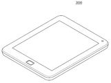
도 8 내지 도 11은 본 발명의 예들에 따른 표시 장치가 적용된 멀티미디어 장치의 예들을 보여준다. 본 발명의 예들에 따른 표시 장치(100~102)는, 도 8에 도시된 바와 같이 모바일 폰 또는 스마트 폰(2000)에 적용될 수 있고, 도 9에 도시된 바와 같이 태블릿 또는 스마트 태블릿(3000)에 적용될 수 있다. 또한, 본 발명의 예들에 따른 표시 장치(100~102)는, 도 10에 도시된 바와 같이 노트북 컴퓨터(4000)에 적용될 수 있고, 도 11에 도시된 바와 같이 텔레비전, 모니터 또는 스마트 텔레비전(5000)에 적용될 수 있다. 8 to 11 show examples of a multimedia device to which a display device according to the exemplary embodiments of the present invention is applied. The
상술한 설명들은 본 발명의 개념을 예시하는 것들이다. 또한, 상술한 내용은 본 발명의 개념을 당업자가 쉽게 이해할 수 있도록 구현한 예들을 나타내고 설명하는 것일 뿐이며, 본 발명은 다른 조합, 변경 및 환경에서 사용될 수 있다. 즉, 본 발명은 본 명세서에 개시된 발명의 범위, 저술한 개시 내용과 균등한 범위 및/또는 당업계의 기술 또는 지식의 범위 내에서 변경 및 수정 등이 가능할 수 있다. 또한, 상술한 실시예들은 당업계에 알려진 다른 상태로의 실시, 그리고 발명의 구체적인 적용 분야 및 용도에서 요구되는 다양한 변경도 가능할 수 있다. 따라서, 상술한 발명의 상세한 설명은 개시된 실시예들은 본 발명을 제한하지 않으며, 첨부된 청구범위는 다른 실시 상태도 포함한다. The foregoing description illustrates the concept of the present invention. In addition, the above description is intended to illustrate and explain the embodiments of the present invention so that those skilled in the art can easily understand the concept of the present invention, and the present invention can be used in other combinations, changes, and environments. That is, the present invention may be modified and modified within the scope of the invention disclosed herein, within the scope of equivalents to the disclosure described herein, and / or within the skill or knowledge of those skilled in the art. It should also be noted that the above-described embodiments may be practiced in other situations known in the art, and various modifications may be possible as are required in the specific applications and applications of the invention. Accordingly, the foregoing description of the invention is not intended to limit the invention to the precise form disclosed, and the appended claims also encompass other embodiments.
1: 표시 소자
TR: 구동 트랜지스터
20: 층간절연막
26: 콘택 플러그
25: 화소 전극
26: 격벽
28: 유기 발광 부재
30: 공통 전극
OLED: 유기 발광 다이오드
32: 봉지막
3, 45a, 45b, 47, 66: 접속 단자
5: 보호막
34, 52, 56: 접착 부재
54, 58: 연결 부재
40: 반도체 패키지
41: 패키지 기판
49: 반도체 칩
60: 회로 기판
62: 프레임
64: 개구부
OR: 표시 영역
BR: 비표시 영역1: display element
TR: driving transistor
20: Interlayer insulating film
26: contact plug
25:
26:
28: organic light emitting member
30: common electrode
OLED: Organic Light Emitting Diode
32: sealing film
3, 45a, 45b, 47, 66: connection terminal
5: Shield
34, 52, 56:
54, 58: connecting member
40: semiconductor package
41: Package substrate
49: Semiconductor chip
60: circuit board
62: frame
64: opening
OR: display area
BR: Non-display area
Claims (10)
상기 표시 영역에서 상기 표시 기판 상에 배치되는 복수개의 단위 표시 소자들;
상기 비표시 영역에서 상기 표시 기판 상에 배치되며 상기 단위 표시 소자와 전기적으로 연결되는 제 1 접속 단자;
상기 비표시 영역에서 상기 표시 기판 상에 배치되는 회로 기판; 및
상기 비표시 영역에서 상기 표시 기판 상에 배치되며 상기 회로 기판과 상기 기 제 1 접속 단자를 전기적으로 연결시키는 반도체 패키지를 포함하되,
상기 반도체 패키지는 평평한 것을 특징으로 하는 패키지 기판을 포함하는 표시 장치. A display substrate including a display region and a non-display region;
A plurality of unit display elements disposed on the display substrate in the display area;
A first connection terminal disposed on the display substrate in the non-display region and electrically connected to the unit display element;
A circuit board disposed on the display substrate in the non-display area; And
And a semiconductor package disposed on the display substrate in the non-display area and electrically connecting the circuit board and the first connection terminal,
Wherein the semiconductor package is flat.
상기 패키지 기판은 하부면에 배치되는 제 2 접속 단자, 상부면에 배치되며 서로 이격되는 제 3 접속 단자와 제 4 접속 단자, 및 상기 패키지 기판을 관통하여 상기 제 2 접속 단자와 상기 제 3 접속 단자를 전기적으로 연결시키는 관통 비아를 더 포함하되,
상기 제 1 접속 단자는 상기 제 2 접속 단자와 전기적으로 연결되고 상기 회로 기판은 상기 제 4 접속 단자와 전기적으로 연결되는 표시 장치. The method according to claim 1,
Wherein the package substrate has a second connection terminal disposed on a lower surface thereof, a third connection terminal and a fourth connection terminal disposed on the upper surface and spaced apart from each other, and a second connection terminal through the package substrate, Further comprising: a through via for electrically connecting the through-
Wherein the first connection terminal is electrically connected to the second connection terminal and the circuit board is electrically connected to the fourth connection terminal.
상기 제 1 접속 단자와 상기 제 2 접속 단자 사이에 개재되어 이들을 전기적으로 연결시키는 제 1 연결 부재를 더 포함하되,
상기 제 1 연결 부재는 이방성 전도성 필름 또는 솔더볼인 표시 장치.3. The method of claim 2,
And a first connection member interposed between the first connection terminal and the second connection terminal to electrically connect the first connection terminal and the second connection terminal,
Wherein the first connecting member is an anisotropic conductive film or a solder ball.
상기 패키지 기판은 단단하거나 유연한 표시 장치.3. The method of claim 2,
Wherein the package substrate is rigid or flexible.
상기 패키지 기판 상에 실장되며 상기 제 3 및 제 4 접속 단자들과 접하는 반도체 칩을 더 포함하되,
상기 반도체 칩의 하부면은 상기 표시 기판의 상부면에 대하여 평행한 표시 장치. 3. The method of claim 2,
And a semiconductor chip mounted on the package substrate and in contact with the third and fourth connection terminals,
Wherein a lower surface of the semiconductor chip is parallel to an upper surface of the display substrate.
상기 회로 기판의 일부분 아래에 상기 패키지 기판이 배치되며,
상기 회로 기판과 상기 표시 기판 사이에 배치되어 상기 회로 기판을 지지하는 브래킷을 더 포함하는 표시 장치. 3. The method of claim 2,
Wherein the package substrate is disposed under a portion of the circuit board,
And a bracket disposed between the circuit board and the display board to support the circuit board.
상기 회로 기판은 하부면에 배치되는 제 5 접속 단자를 더 포함하며,
상기 제 5 접속 단자와 상기 제 4 접속 단자 사이에 개재되며 이들을 전기적으로 연결시키는 제 2 연결 부재를 더 포함하는 표시 장치.The method according to claim 6,
The circuit board further includes a fifth connection terminal disposed on a lower surface thereof,
And a second connection member interposed between the fifth connection terminal and the fourth connection terminal and electrically connecting the fifth connection terminal and the fourth connection terminal.
상기 제 2 연결 부재는 이방성 전도성 필름 또는 솔더볼인 표시 장치.8. The method of claim 7,
Wherein the second connecting member is an anisotropic conductive film or a solder ball.
상기 회로 기판은 상기 표시 기판 상에 부착되는 표시 장치. 3. The method of claim 2,
Wherein the circuit board is attached to the display substrate.
상기 회로 기판은 상부면에 배치되는 제 5 접속 단자를 더 포함하며,
상기 제 5 접속 단자와 상기 제 4 접속 단자를 전기적으로 연결시키는 제 3 연결 부재를 더 포함하는 표시 장치. 10. The method of claim 9,
The circuit board further includes a fifth connection terminal disposed on an upper surface thereof,
And a third connection member for electrically connecting the fifth connection terminal and the fourth connection terminal.
Priority Applications (2)
| Application Number | Priority Date | Filing Date | Title |
|---|---|---|---|
| KR1020130067235A KR20140144963A (en) | 2013-06-12 | 2013-06-12 | Display device |
| US14/279,170 US20140367659A1 (en) | 2013-06-12 | 2014-05-15 | Display devices |
Applications Claiming Priority (1)
| Application Number | Priority Date | Filing Date | Title |
|---|---|---|---|
| KR1020130067235A KR20140144963A (en) | 2013-06-12 | 2013-06-12 | Display device |
Publications (1)
| Publication Number | Publication Date |
|---|---|
| KR20140144963A true KR20140144963A (en) | 2014-12-22 |
Family
ID=52018455
Family Applications (1)
| Application Number | Title | Priority Date | Filing Date |
|---|---|---|---|
| KR1020130067235A KR20140144963A (en) | 2013-06-12 | 2013-06-12 | Display device |
Country Status (2)
| Country | Link |
|---|---|
| US (1) | US20140367659A1 (en) |
| KR (1) | KR20140144963A (en) |
Families Citing this family (4)
| Publication number | Priority date | Publication date | Assignee | Title |
|---|---|---|---|---|
| CN110164880B (en) * | 2015-06-09 | 2022-05-10 | 群创光电股份有限公司 | Display device |
| JP6622923B2 (en) * | 2016-02-18 | 2019-12-18 | アップル インコーポレイテッドApple Inc. | Backplane structure and process for microdrivers and microLEDs |
| CN108281472B (en) * | 2018-02-05 | 2021-01-22 | 京东方科技集团股份有限公司 | Display assembly, display device and manufacturing method |
| CN109873090B (en) | 2019-03-29 | 2021-10-29 | 合肥鑫晟光电科技有限公司 | Packaging structure, display substrate, display device and packaging method of display device |
Family Cites Families (2)
| Publication number | Priority date | Publication date | Assignee | Title |
|---|---|---|---|---|
| TW465122B (en) * | 1999-12-15 | 2001-11-21 | Semiconductor Energy Lab | Light-emitting device |
| KR100720143B1 (en) * | 2005-12-13 | 2007-05-18 | 삼성전자주식회사 | Display device |
-
2013
- 2013-06-12 KR KR1020130067235A patent/KR20140144963A/en not_active Application Discontinuation
-
2014
- 2014-05-15 US US14/279,170 patent/US20140367659A1/en not_active Abandoned
Also Published As
| Publication number | Publication date |
|---|---|
| US20140367659A1 (en) | 2014-12-18 |
Similar Documents
| Publication | Publication Date | Title |
|---|---|---|
| WO2019085195A1 (en) | Spliced display device | |
| CN108766994B (en) | Organic light emitting display panel and organic light emitting display device | |
| US11307693B2 (en) | Display device having shaped sealing member | |
| KR101736930B1 (en) | Flexible organic light emitting display device | |
| TWI478128B (en) | Light emitting diode display panel | |
| US20190305070A1 (en) | Display device | |
| US10551700B2 (en) | Display apparatus including a backlight assembly | |
| US11522143B2 (en) | Display device having a circuit board connected to a signal line by a conductive material in a substrate | |
| CN111048568B (en) | Display panel and display device | |
| WO2019000912A1 (en) | Display panel and manufacturing method therefor, and display apparatus | |
| US11217638B2 (en) | Display device | |
| KR20140144963A (en) | Display device | |
| US20190189733A1 (en) | Array Substrate, Electroluminescent Display Panel and Display Device | |
| US20230205347A1 (en) | Display device | |
| KR102322766B1 (en) | display device | |
| US20230093856A1 (en) | Touch sensing unit and display device including same | |
| CN112382646B (en) | OLED display panel and touch display screen | |
| JP2020187234A (en) | Display | |
| US20240023414A1 (en) | Display device and method of providing the same | |
| US20240121996A1 (en) | Display device | |
| US20230389389A1 (en) | Display device | |
| US20240118775A1 (en) | Display device | |
| KR20150074453A (en) | Flexible display device | |
| KR20240050990A (en) | Display device | |
| KR20230085242A (en) | Display panel and method for fabricating the same |
Legal Events
| Date | Code | Title | Description |
|---|---|---|---|
| WITN | Application deemed withdrawn, e.g. because no request for examination was filed or no examination fee was paid |