KR20140129231A - Atomic layer deposition lithography - Google Patents
Atomic layer deposition lithography Download PDFInfo
- Publication number
- KR20140129231A KR20140129231A KR1020147026300A KR20147026300A KR20140129231A KR 20140129231 A KR20140129231 A KR 20140129231A KR 1020147026300 A KR1020147026300 A KR 1020147026300A KR 20147026300 A KR20147026300 A KR 20147026300A KR 20140129231 A KR20140129231 A KR 20140129231A
- Authority
- KR
- South Korea
- Prior art keywords
- monolayer
- material layer
- region
- forming features
- gas mixture
- Prior art date
Links
Images


Classifications
-
- G—PHYSICS
- G03—PHOTOGRAPHY; CINEMATOGRAPHY; ANALOGOUS TECHNIQUES USING WAVES OTHER THAN OPTICAL WAVES; ELECTROGRAPHY; HOLOGRAPHY
- G03F—PHOTOMECHANICAL PRODUCTION OF TEXTURED OR PATTERNED SURFACES, e.g. FOR PRINTING, FOR PROCESSING OF SEMICONDUCTOR DEVICES; MATERIALS THEREFOR; ORIGINALS THEREFOR; APPARATUS SPECIALLY ADAPTED THEREFOR
- G03F7/00—Photomechanical, e.g. photolithographic, production of textured or patterned surfaces, e.g. printing surfaces; Materials therefor, e.g. comprising photoresists; Apparatus specially adapted therefor
- G03F7/16—Coating processes; Apparatus therefor
-
- H—ELECTRICITY
- H01—ELECTRIC ELEMENTS
- H01L—SEMICONDUCTOR DEVICES NOT COVERED BY CLASS H10
- H01L21/00—Processes or apparatus adapted for the manufacture or treatment of semiconductor or solid state devices or of parts thereof
- H01L21/02—Manufacture or treatment of semiconductor devices or of parts thereof
- H01L21/027—Making masks on semiconductor bodies for further photolithographic processing not provided for in group H01L21/18 or H01L21/34
- H01L21/0271—Making masks on semiconductor bodies for further photolithographic processing not provided for in group H01L21/18 or H01L21/34 comprising organic layers
- H01L21/0273—Making masks on semiconductor bodies for further photolithographic processing not provided for in group H01L21/18 or H01L21/34 comprising organic layers characterised by the treatment of photoresist layers
- H01L21/0274—Photolithographic processes
-
- G—PHYSICS
- G03—PHOTOGRAPHY; CINEMATOGRAPHY; ANALOGOUS TECHNIQUES USING WAVES OTHER THAN OPTICAL WAVES; ELECTROGRAPHY; HOLOGRAPHY
- G03F—PHOTOMECHANICAL PRODUCTION OF TEXTURED OR PATTERNED SURFACES, e.g. FOR PRINTING, FOR PROCESSING OF SEMICONDUCTOR DEVICES; MATERIALS THEREFOR; ORIGINALS THEREFOR; APPARATUS SPECIALLY ADAPTED THEREFOR
- G03F7/00—Photomechanical, e.g. photolithographic, production of textured or patterned surfaces, e.g. printing surfaces; Materials therefor, e.g. comprising photoresists; Apparatus specially adapted therefor
- G03F7/0035—Multiple processes, e.g. applying a further resist layer on an already in a previously step, processed pattern or textured surface
-
- G—PHYSICS
- G03—PHOTOGRAPHY; CINEMATOGRAPHY; ANALOGOUS TECHNIQUES USING WAVES OTHER THAN OPTICAL WAVES; ELECTROGRAPHY; HOLOGRAPHY
- G03F—PHOTOMECHANICAL PRODUCTION OF TEXTURED OR PATTERNED SURFACES, e.g. FOR PRINTING, FOR PROCESSING OF SEMICONDUCTOR DEVICES; MATERIALS THEREFOR; ORIGINALS THEREFOR; APPARATUS SPECIALLY ADAPTED THEREFOR
- G03F7/00—Photomechanical, e.g. photolithographic, production of textured or patterned surfaces, e.g. printing surfaces; Materials therefor, e.g. comprising photoresists; Apparatus specially adapted therefor
- G03F7/16—Coating processes; Apparatus therefor
- G03F7/165—Monolayers, e.g. Langmuir-Blodgett
-
- G—PHYSICS
- G03—PHOTOGRAPHY; CINEMATOGRAPHY; ANALOGOUS TECHNIQUES USING WAVES OTHER THAN OPTICAL WAVES; ELECTROGRAPHY; HOLOGRAPHY
- G03F—PHOTOMECHANICAL PRODUCTION OF TEXTURED OR PATTERNED SURFACES, e.g. FOR PRINTING, FOR PROCESSING OF SEMICONDUCTOR DEVICES; MATERIALS THEREFOR; ORIGINALS THEREFOR; APPARATUS SPECIALLY ADAPTED THEREFOR
- G03F7/00—Photomechanical, e.g. photolithographic, production of textured or patterned surfaces, e.g. printing surfaces; Materials therefor, e.g. comprising photoresists; Apparatus specially adapted therefor
- G03F7/16—Coating processes; Apparatus therefor
- G03F7/167—Coating processes; Apparatus therefor from the gas phase, by plasma deposition
Landscapes
- Physics & Mathematics (AREA)
- General Physics & Mathematics (AREA)
- Engineering & Computer Science (AREA)
- Plasma & Fusion (AREA)
- Computer Hardware Design (AREA)
- Manufacturing & Machinery (AREA)
- Condensed Matter Physics & Semiconductors (AREA)
- Microelectronics & Electronic Packaging (AREA)
- Power Engineering (AREA)
- Chemical Vapour Deposition (AREA)
- Photosensitive Polymer And Photoresist Processing (AREA)
- Exposure Of Semiconductors, Excluding Electron Or Ion Beam Exposure (AREA)
- Drying Of Semiconductors (AREA)
Abstract
원자 층 증착 리소그래피 프로세스를 수행하기 위한 방법들 및 장치가 본원 개시 내용에서 제공된다. 일 실시예에서, 디바이스 내의 재료 층 상에 피쳐들을 형성하기 위한 방법은, 기판 표면 상에 재료 층의 제 1 단분자층(monolayer)을 형성하기 위해, 프로세싱 챔버 내에 배치된 기판의 표면에 제 1 반응물 가스 혼합물(reactant gas mixture)을 펄싱(pulsing)하는 단계; 상기 제 1 단분자층의 제 1 영역을 처리하기 위해, 에너제틱 복사선(energetic radiation)을 지향시키는 단계; 및 상기 제 1 단분자층의 제 2 영역 상에서 제 2 단분자층을 선택적으로 형성하기 위해, 기판 표면에 제 2 반응물 가스 혼합물을 펄싱하는 단계를 포함한다. Methods and apparatus for performing atomic layer deposition lithographic processes are provided herein. In one embodiment, a method for forming features on a material layer in a device includes forming a first monolayer of a material layer on a substrate surface by depositing a first reactant gas on a surface of a substrate disposed in the processing chamber, Pulsing the reactant gas mixture; Directing energetic radiation to process a first region of the first monolayer; And pulsing a second reactant gas mixture on the substrate surface to selectively form a second monolayer on the second region of the first monolayer.

Description
본 발명은 일반적으로, 원자 층 증착 리소그래피 프로세스를 위한 방법들 및 장치에 관한 것이고, 보다 구체적으로는, 반도체 분야에서 기판 표면 상에 피쳐들(features)/구조들을 형성하기 위해 리소그래피 프로세스와 함께 원자 층 증착 프로세스를 이용하기 위한 방법들 및 장치에 관한 것이다. FIELD OF THE INVENTION The present invention relates generally to methods and apparatus for atomic layer deposition lithography processes and more particularly to methods and apparatus for atomic layer deposition processes in conjunction with a lithographic process to form features / To methods and apparatus for utilizing a deposition process.
집적 회로들은, 단일 칩 상에서 수백 만개의 구성요소들(예를 들어, 트랜지스터들, 커패시터들 및 저항기들)을 포함할 수 있는 복잡한 디바이스들로 발전하였다. 칩 디자인들의 발전은 보다 빠른 회로망 및 보다 큰 회로 밀도를 지속적으로 요구한다. 보다 큰 회로 밀도에 대한 요구들은 집적 회로 구성요소들의 치수들의 감소를 필요로 한다. Integrated circuits have evolved into complex devices that can include millions of components (e.g., transistors, capacitors, and resistors) on a single chip. Advances in chip designs continue to require faster circuitry and larger circuit densities. The demands for greater circuit density require a reduction in the dimensions of the integrated circuit components.
집적 회로 구성요소들의 치수들이 (예를 들어, 서브-미크론 치수들로) 감소됨에 따라, 보다 많은 요소(element)들이 반도체 집적 회로의 주어진 면적 내에 배치될 것이 요구된다. 따라서, 리소그래피 프로세스는, 훨씬 더 작은 피쳐들을 기판 상에 손상없이 정확하게 그리고 정밀하게 전사(transfer)시키는 데에 있어서 점점 더 어려움을 갖게 되었다. 피쳐들을 기판 상에 정밀하고 정확하게 전사시키기 위하여, 요구되는 고 분해능(resolution)의 리소그래피 프로세스는, 노광을 위해 요구되는 파장 범위의 복사선을 제공할 수 있는 적절한 광 소스를 가질 것을 필요로 한다. 또한, 리소그래피 프로세스는 최소의 구조 및/또는 임계 치수 변경(alternation)을 가지면서 피쳐들을 포토레지스트 층 상에 전사시킬 것을 필요로 한다. 최근에, 기판 상에 인쇄될 수 있는 최소 크기를 더 감소시키기 위해 짧은 노광 파장들을 제공하기 위하여, 극자외선(EUV) 복사선 소스가 이용되어 왔다. 그러나, 그러한 작은 치수들에서는, 후속 에칭 프로세스 동안 포토레지스트 층의 붕괴 또는 손상이 종종 발생되고, 그에 따라 기판 표면 상에 구조들을 성공적으로 전사시키지 못하게 되는 결과를 초래한다. As the dimensions of the integrated circuit components are reduced (e.g., to sub-micron dimensions), it is required that more elements be placed within a given area of the semiconductor integrated circuit. Thus, lithographic processes have become increasingly difficult to accurately and precisely transfer much smaller features onto a substrate without damage. In order to transfer precisely and accurately the features onto the substrate, the required high resolution lithography process needs to have an appropriate light source capable of providing radiation in the wavelength range required for exposure. In addition, the lithographic process requires transferring features onto the photoresist layer with minimal structure and / or critical dimension alternation. Recently, extreme ultraviolet (EUV) radiation sources have been used to provide short exposure wavelengths to further reduce the minimum size that can be printed on a substrate. However, such small dimensions result in the collapse or damage of the photoresist layer during subsequent etching processes often resulting in failure to successfully transfer structures onto the substrate surface.
통상적인 리소그래피 프로세스에서, 기판 상에 배치된 포토레지스트 층의 일부 부분들은 화학적 변환(transformation)을 겪기 위해 입사 복사선에 노광된다. 전형적인 포지티브 톤(positive tone) 노광 프로세스에서, 화학적 변환을 겪는, 포토레지스트 층의 노광된 부분은 현상 프로세스 동안 수성 용액(aqueous base solution)을 이용하여 제거된다. 마이크로전자 디바이스 상에 형성되는 피쳐 크기들이 지속적으로 축소됨에 따라, 물의 표면 장력 및 모세관력들에 의해 유발되는 이미지 붕괴로 인해 수성 용액 현상제가 문제가 될 수 있다. 또한, 용액 기반 현상액(solution based developer)들은 현상 프로세스 이후에 기판 상에 원치않는 오염물질들을 남기는 경향이 있고, 그에 의해 기판 청정도(cleanliness)에 부정적인 영향을 미치는 경향이 있다. In a typical lithographic process, some portions of the photoresist layer disposed on the substrate are exposed to incident radiation to undergo chemical transformation. In a typical positive tone exposure process, the exposed portions of the photoresist layer, undergoing chemical conversion, are removed using an aqueous base solution during the development process. As feature sizes formed on microelectronic devices are continually shrunk, aqueous solution developers can become problematic due to image disruption caused by surface tension and capillary forces of water. In addition, solution based developers tend to leave unwanted contaminants on the substrate after the development process and thereby tend to negatively impact substrate cleanliness.
그에 따라, 요구되는 임계 치수들로 기판 표면 상에 정밀한 구조 전사를 달성하기 위해, 구조 손상이 최소화되는 상태로 리소그래피 프로세스에 대한 프로세스 결함들을 제어하기 위한 방법 및 장치가 필요하다. Accordingly, there is a need for a method and apparatus for controlling process defects for a lithographic process with structural damage minimized to achieve precise structural transfer on the substrate surface with the critical dimensions required.
원자 층 증착 리소그래피 프로세스를 수행하기 위한 방법들 및 장치가 본원 개시 내용에서 제공된다. 일 실시예에서, 디바이스 내의 재료 층 상에 피쳐들을 형성하기 위한 방법은, 기판 표면 상에 재료 층의 제 1 단분자층(monolayer)을 형성하기 위해, 프로세싱 챔버 내에 배치된 기판의 표면에 제 1 반응물 가스 혼합물(reactant gas mixture)을 펄싱(pulsing)하는 단계; 상기 제 1 단분자층의 제 1 영역을 처리하기 위해, 에너제틱 복사선(energetic radiation)을 지향시키는 단계; 및 상기 제 1 단분자층의 제 2 영역 상에서 제 2 단분자층을 선택적으로 형성하기 위해, 기판 표면에 제 2 반응물 가스 혼합물을 펄싱하는 단계를 포함한다. Methods and apparatus for performing atomic layer deposition lithographic processes are provided herein. In one embodiment, a method for forming features on a material layer in a device includes forming a first monolayer of a material layer on a substrate surface by depositing a first reactant gas on a surface of a substrate disposed in the processing chamber, Pulsing the reactant gas mixture; Directing energetic radiation to process a first region of the first monolayer; And pulsing a second reactant gas mixture on the substrate surface to selectively form a second monolayer on the second region of the first monolayer.
다른 실시예에서, 디바이스 내의 재료 층 상에 피쳐들을 형성하기 위한 방법은, 원자 층 증착 프로세스에서 수행되는 제 1 반응물 가스 혼합물의 펄스에 의해 증착되는 재료 층의 제 1 단분자층의 제 1 영역을 처리하기 위해, 광 복사선을 지향시키는 단계; 상기 재료 층의 제 1 단분자층 상에 제 2 단분자층을 형성하기 위해 원자 층 증착 프로세스를 수행하는 것을 계속하는 단계; 및 상기 광 복사선에 의해 처리된 제 1 영역 내의 상기 제 1 단분자층을 제거하는 단계를 포함한다. In another embodiment, a method for forming features on a material layer in a device comprises processing a first region of a first monolayer of a material layer deposited by a pulse of a first reactant gas mixture performed in an atomic layer deposition process Directing an optical radiation; Continuing to perform an atomic layer deposition process to form a second monolayer on the first monolayer of the material layer; And removing the first monolayer within the first region processed by the optical radiation.
또 다른 실시예에서, 원자 층 증착 프로세스 및 리소그래피 프로세스를 수행하도록 구성된 프로세싱 챔버는, 챔버 본체(chamber body) ― 상기 챔버 본체 상에는, 상기 챔버 본체 내에 내부 프로세싱 용적을 정의하는 챔버 덮개(chamber lid)가 배치됨 ― ; 상기 내부 프로세싱 영역 내에 배치된 페디스털(pedestal); 반응물 가스를 상기 내부 프로세싱 영역 내로 전달하기 위해, 상기 챔버 본체 상에 배치된 가스 전달 시스템; 에너제틱 복사선을 상기 내부 프로세싱 영역을 향해서 지향시키기 위해, 상기 챔버 덮개 아래에 배치된 에너지 빔 소스; 및 상기 에너지 빔 소스와 상기 페디스털 사이에 배치된 마스크를 포함한다. In another embodiment, a processing chamber configured to perform an atomic layer deposition process and a lithographic process includes a chamber body on which a chamber lid defining an internal processing volume is defined within the chamber body Deployed -; A pedestal disposed within the internal processing area; A gas delivery system disposed on the chamber body for delivering reagent gas into the internal processing region; An energy beam source disposed below said chamber lid to direct an energetic radiation towards said internal processing region; And a mask disposed between the energy beam source and the pedestal.
본 발명의 상기 열거된 특징들이 상세히 이해될 수 있는 방식으로 앞서 간략히 요약된 본 발명의 보다 구체적인 설명이 실시예들을 참조로 하여 이루어질 수 있는데, 이러한 실시예들 중 일부는 첨부된 도면들에 예시되어 있다. 그러나, 첨부된 도면들은 본 발명의 단지 전형적인 실시예들을 도시하는 것이므로 본 발명의 범위를 제한하는 것으로 간주되지 않아야 한다는 것이 주목되어야 하는데, 이는 본 발명이 다른 균등하게 유효한 실시예들을 허용할 수 있기 때문이다.
도 1은 본 발명의 일 실시예를 수행하기에 적합한 원자 층 증착(ALD) 리소그래피 프로세싱 챔버의 일 실시예의 단면도를 도시한다.
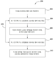
도 2는 도 1에 도시된 ALD 리소그래피 프로세싱 챔버를 이용하여 수행될 수 있는 ALD 리소그래피 프로세스를 수행하기 위한 흐름도를 도시한다.
도 3a-3e는 본 발명의 일 실시예에 따라 ALD 리소그래피 프로세스를 수행하는 상이한 스테이지들 동안의 반도체 디바이스의 횡단면도들을 도시한다.
이해를 돕기 위해, 도면들 간에 공통적인 동일한 엘리먼트들을 가리키기 위해, 가능한 경우, 동일한 도면부호들이 사용되었다. 추가의 언급없이도, 일 실시예의 엘리먼트들 및 피쳐들이 다른 실시예들에 유리하게 통합될 수 있음이 고려된다.
그러나, 첨부된 도면들은 본 발명의 단지 전형적인 실시예들을 도시하는 것이므로 본 발명의 범위를 제한하는 것으로 간주되지 않아야 한다는 것이 주목되어야 하는데, 이는 본 발명이 다른 균등하게 유효한 실시예들을 허용할 수 있기 때문이다. A more particular description of the invention, briefly summarized above, in such a manner that the recited features of the invention may be understood in detail, may be made by reference to embodiments, some of which are illustrated in the accompanying drawings have. It should be noted, however, that the appended drawings illustrate only typical embodiments of this invention and are therefore not to be considered limiting of its scope, for the invention may admit to other equally effective embodiments to be.
Figure 1 illustrates a cross-sectional view of one embodiment of an atomic layer deposition (ALD) lithographic processing chamber suitable for carrying out an embodiment of the present invention.
2 illustrates a flow chart for performing an ALD lithography process that may be performed using the ALD lithographic processing chamber shown in FIG.
3A-3E illustrate cross-sectional views of a semiconductor device during different stages of performing an ALD lithographic process in accordance with one embodiment of the present invention.
To facilitate understanding, identical reference numerals have been used, where possible, to designate identical elements that are common to the figures. It is contemplated that elements and features of one embodiment may be advantageously incorporated into other embodiments without further recitation.
It should be noted, however, that the appended drawings illustrate only typical embodiments of this invention and are therefore not to be considered limiting of its scope, for the invention may admit to other equally effective embodiments to be.
원자 층 증착(ALD) 리소그래피 프로세스를 수행하기 위한 방법들 및 장치가 본원 개시 내용에서 제공된다. 그러한 ALD 리소그래피 프로세스는, 통상의 포토레지스트 층 및/또는 하드마스크 층을 이용하지 않으면서, 기판 표면 상에 피쳐들을 형성하기 위해 리소그래피 프로세스와 함께 ALD 프로세스를 이용한다. ALD 리소그래피 프로세싱 챔버는; 원자 층 증착된 층(atomic layer deposited layer)을 증착하기 위한, 그리고 상기 원자 층 증착된 층 상에 피쳐들/구조들을 형성하기 위해 리소그래피 프로세스(예를 들어, 에너지 빔 처리 프로세스)를 수행하기 위한, 이중 기능을 제공한다. 기판은, 이를 테면 실리콘, 실리콘 이산화물, 도핑된 실리콘, 게르마늄, 갈륨 비소, 유리, 및 사파이어와 같은 하나 또는 그 초과의 비전도성 재료들을 포함할 수 있다. 또한, 기판은, 이를 테면 실리콘 이산화물, 올가노실리케이트(organosilicate)들, 및 탄소 도핑된 실리콘 산화물들과 같은 유전체 재료들을 포함할 수 있다. 또한, 적용예에 따라서, 기판은, 이를 테면 금속 질화물들 및 금속 합금들과 같은 임의의 다른 재료들을 포함할 수 있다. 하나 또는 그 초과의 실시예들에서, 기판은, 이를 테면 플러그, 비아, 콘택, 및 와이어와 같이 후속하여 상부에 형성되는 배선 피쳐와의 연결을 용이하게 하기 위해, 게이트 전극 층 및 게이트 유전체를 포함하는 게이트 구조를 형성할 수 있다. 기판은, 집적 회로, 태양 전지(solar), MEMs 또는 다른 디바이스 제조를 위해 이용될 수 있다. Methods and apparatus for performing atomic layer deposition (ALD) lithography processes are provided herein. Such an ALD lithography process utilizes an ALD process in conjunction with a lithographic process to form features on a substrate surface, without using a conventional photoresist layer and / or a hard mask layer. The ALD lithographic processing chamber comprising: A method for depositing an atomic layer deposited layer and for performing a lithographic process (e.g., an energy beam processing process) to form features / structures on the atomic layer deposited layer, Provides dual functionality. The substrate may comprise one or more nonconductive materials such as, for example, silicon, silicon dioxide, doped silicon, germanium, gallium arsenide, glass, and sapphire. The substrate may also include dielectric materials such as silicon dioxide, organosilicates, and carbon doped silicon oxides. Further, depending on the application, the substrate may comprise any other materials such as metal nitrides and metal alloys, for example. In one or more embodiments, the substrate includes a gate electrode layer and a gate dielectric, such as plugs, vias, contacts, and wires, to facilitate subsequent connection with interconnect features formed thereon The gate structure can be formed. The substrate can be used for the manufacture of integrated circuits, solar, MEMs or other devices.
또한, 기판은 임의의 특정한 크기 또는 형상으로 제한되지 않는다. 기판은, 200 mm 직경, 300 mm 직경 또는 다른 직경들(이를 테면, 특히, 450 mm)을 갖는 둥근 기판일 수 있다. 또한, 기판은, 이를 테면, 평판 디스플레이들의 제조에서 이용되는 다각형 유리 기판과 같은, 임의의 다각형, 정사각형, 직사각형, 곡선형(curved), 또는 다른 비-원형 워크피스(workpiece)일 수 있다. Further, the substrate is not limited to any particular size or shape. The substrate may be a round substrate having a diameter of 200 mm, a diameter of 300 mm, or other diameters (such as 450 mm in particular). The substrate may also be any polygonal, square, rectangular, curved, or other non-circular workpiece, such as a polygonal glass substrate used in the manufacture of flat panel displays, for example.
본 발명은, 증착된 재료 층 상에 피쳐들/구조들을 형성하기 위해, ALD 프로세스 및 그에 후속되는 리소그래피 프로세스(예를 들어, 에너지 빔 처리 프로세스)에 의해 기판 상에 재료 층을 증착/형성하기 위한 방법들을 제공한다. 프로세스는, 기판 표면 상에 피쳐들/구조들을 전사시키는 것을 보조하기 위해, 통상의 포토레지스트 층 및/또는 하드마스크 층을 이용하지 않으면서, 기판 표면 상에 요구되는 작은 임계 치수를 갖는 피쳐들/구조들을 효과적으로 형성할 수 있으며, 그에 의해 제조 사이클 시간 및 비용을 개선할 수 있으며, 그리고 제조 복잡성을 줄일 수 있다. 유익하게는, ALD와 리소그래피 프로세스 양자 모두는 단일 챔버에서 수행될 수 있다. The present invention provides a method for depositing / forming a layer of material on a substrate by an ALD process and a subsequent lithographic process (e.g., an energy beam process) to form features / structures on the deposited material layer Methods. The process may be used to transfer features / structures with small critical dimensions required on the substrate surface, without using conventional photoresist layers and / or hardmask layers to assist in transferring features / Structures can be effectively formed, thereby improving manufacturing cycle time and cost, and reducing manufacturing complexity. Advantageously, both the ALD and the lithography process can be performed in a single chamber.
도 1은 ALD 리소그래피 프로세싱 챔버(134)의 일 실시예의 개략적인 단면도이다. ALD 리소그래피 프로세싱 챔버(134)는, 이를 테면 ALD 또는 화학 기상 증착(CVD)과 같은 순환 증착(cyclic deposition)을 위해 구성된 가스 전달 장치(130)를 포함한다. 여기에서 사용되는 바와 같은 ALD 및 CVD의 용어들은, 기판 구조 위에 얇은 층을 증착하기 위해 반응물들을 순차적으로 도입하는 것을 지칭한다. 반응물들의 순차적인 도입을 반복하여, 복수의 얇은 층들을 증착함으로써, 등각적인(conformal) 층을 요구되는 두께로 증착할 수 있다. 챔버(134)는 또한, 리소그래피 프로세스와 함께 다른 증착 기술들을 위해 구성될 수 있다. FIG. 1 is a schematic cross-sectional view of one embodiment of an ALD
챔버(134)는, 측벽들(131) 및 바닥부(bottom)(132)를 갖는 챔버 본체(129)를 포함한다. 챔버 본체(129)를 통해 형성되는 슬릿 밸브 터널(slit valve tunnel)(133)은, 이를 테면 200 mm, 300 mm 또는 450 mm 반도체 기판 또는 유리 기판과 같은 기판(102)을 챔버(134)에 전달하며 그리고 챔버(134)로부터 인출(retrieve)하기 위한 로봇(미도시)을 위한 액세스(access)를 제공한다. The
기판 지지부(192)가 챔버(134) 내에 배치되어, 프로세싱 동안 기판(102)을 지지한다. 기판 지지부(192)는, 기판 지지부(192) 및 그 상부에 배치된 기판(102)을 상승 및 하강시키기 위한 리프트(lift)(114)에 장착된다. 리프트 플레이트(116)가, 리프트 플레이트(116)의 높이(elevation)를 제어하는 리프트 플레이트 액추에이터(118)에 연결된다. 기판 지지부(192)를 통해 이동가능하게 배치된 핀들(120)을 상승 및 하강시키기 위해, 리프트 플레이트(116)가 상승 및 하강될 수 있다. 핀들(120)은 기판 지지부(192)의 표면 위에서 기판(102)을 상승 및 하강시키기 위해 이용된다. 기판 지지부(192)는, 프로세싱 동안 기판(102)을 기판 지지부(192)의 표면에 대해 고정하기 위해, 진공 척, 정전기 척, 또는 클램프 링을 포함할 수 있다. A
기판 지지부(192) 상부에 배치된 기판(102)을 가열하기 위해, 기판 지지부(192)가 가열될 수 있다. 예를 들어, 기판 지지부(192)는, 저항성 히터와 같은 매립형 가열 요소(embedded heating element)를 이용하여 가열될 수 있거나, 기판 지지부(192) 위에 배치된 가열 램프들과 같은 복사 열을 이용하여 가열될 수 있다. 퍼지 링(purge ring)(122)이 기판 지지부(192) 상에 배치되어, 기판(102)의 둘레 부분(peripheral portion) 상에서의 증착을 방지하기 위해 기판(102)의 둘레 부분에 퍼지 가스를 제공하는 퍼지 채널(124)을 정의할 수 있다. In order to heat the
가스 전달 장치(130)가 챔버 본체(129)의 상부 부분에 배치되어, 이를 테면 프로세스 가스 및/또는 퍼지 가스와 같은 가스를 챔버(134)에 제공한다. 펌핑 시스템(178)이 펌핑 채널(179)과 소통하여, 챔버(134)로부터 임의의 요구되는 가스들을 배기하고, 챔버(134)의 펌핑 구역(166) 내부에서 요구되는 압력 또는 요구되는 압력 범위를 유지하는 것을 돕는다. A
일 실시예에서, 가스 전달 장치(130)는, 2개의 유사한 밸브들(142A, 142B)로부터 가스 유동들을 제공하기 위한 가스 유입구들(137A, 137B)을 갖는 팽창(expanding) 채널(190)을 포함한다. 밸브들(142A, 142B)로부터의 가스 유동들은 함께 및/또는 개별적으로 제공될 수 있다. In one embodiment, the
하나의 구성에서, 밸브(142A) 및 밸브(142B)는, 개별적인 반응물 가스 소스들에 커플링되지만, 동일한 퍼지 가스 소스에 커플링된다. 예를 들어, 밸브(142A)는 반응물 가스 소스(138)에 커플링되고, 밸브(142B)는 반응물 가스 소스(139)에 커플링되며, 그리고 양 밸브들(142A, 142B)은 퍼지 가스 소스(140)에 커플링된다. 각각의 밸브(142A, 142B)는 밸브 시트 조립체(valve seat assembly)(144A, 144B)를 갖는 전달 라인(143A, 143B)을 포함하고, 밸브 시트 조립체(146A, 146B)를 갖는 퍼지 라인(145A, 145B)을 포함한다. 전달 라인(143A, 143B)은 반응물 가스 소스(138, 139)과 소통하며, 그리고 팽창 채널(190)의 가스 유입구(137A, 137B)와 소통한다. 전달 라인(143A, 143B)의 밸브 시트 조립체(144A, 144B)는 반응물 가스 소스(138, 139)로부터 팽창 채널(190)로의 반응물 가스의 유동을 제어한다. 퍼지 라인(145A, 145B)은 퍼지 가스 소스(140)과 소통하며, 그리고 전달 라인(143A, 143B)의 밸브 시트 조립체(144A, 144B) 하류의 전달 라인(143A, 143B)과 교차한다(intersect). 퍼지 라인(145A, 145B)의 밸브 시트 조립체(146A, 146B)는 퍼지 가스 소스(140)로부터 전달 라인(143A, 143B)으로의 퍼지 가스의 유동을 제어한다. 반응물 가스 소스(138, 139)로부터 반응물 가스들을 전달하기 위해 캐리어 가스가 이용된다면, 동일한 가스가 캐리어 가스 및 퍼지 가스로서 이용된다(즉, 아르곤 가스가 캐리어 가스 및 퍼지 가스로서 이용된다). In one configuration,
밸브의 밸브 시트 조립체(144A, 144B)가 폐쇄될 때 전달 라인(143A, 143B)으로부터의 반응물 가스의 플러싱(flushing)을 가능하게 하기 위해, 각각의 밸브(142A, 142B)는 제로 사부피(zero dead volume) 밸브일 수 있다. 예를 들어, 퍼지 라인(145A, 145B)은 전달 라인(143A, 143B)의 밸브 시트 조립체(144A, 144B) 근처에 배치될 수 있다. 밸브 시트 조립체(144A, 144B)가 폐쇄될 때, 퍼지 라인(145A, 145B)은 전달 라인(143A, 143B)을 플러싱하기 위해 퍼지 가스를 제공할 수 있다. 도시된 실시예에서, 개방될 때 퍼지 가스가 밸브 시트 조립체(144A, 144B) 내로 직접적으로 전달되지 않도록, 퍼지 라인(145A, 145B)은 전달 라인(143A, 143B)의 밸브 시트 조립체(144A, 144B)로부터 약간 이격되어 위치된다. 여기에서 사용되는 바와 같은 제로 사부피 밸브는, 무시할 수 있는 사부피를 갖는(즉, 반드시 제로 사부피는 아니다) 밸브로서 정의된다. 각각의 밸브(142A, 142B)는 반응물 가스(138, 139) 및 퍼지 가스(140)의 조합된 가스 유동 및/또는 개별적인 가스 유동을 제공하도록 구성될 수 있다. 퍼지 라인(145A)의 밸브 시트 조립체(146A)의 격막(diaphragm)을 개방 및 폐쇄시킴으로써, 퍼지 가스의 펄스들이 제공될 수 있다. 전달 라인(143A)의 격막 밸브 시트(144A)를 개방 및 폐쇄시킴으로써, 반응물 가스 소스(138)로부터의 반응물 가스의 펄스들이 제공될 수 있다. Each
전력 소스(103)가, 챔버 본체(129) 상에 배치된 덮개(105)에 커플링된다. 전력 소스(103)는 그 전력 소스(103) 아래에 배치된 에너지 빔 소스(106)에 전력을 제공하도록 구성되며, 에너지 빔 소스(106)는 전력 소스(103)와 에너지 빔 소스(106) 사이에 형성된 개구(104)를 통해 전력 소스(103)에 연결된다. 일 실시예에서, 에너지 빔 소스(106)는, 이를 테면 수은 마이크로파 아크 램프들, 펄스형 크세논 플래시 램프들, 고효율 UV 발광 다이오드 어레이들, 및 전자 빔 발생기들과 같은, UV 광 또는 다른 에너지 복사선을 제공할 수 있는 임의의 적합한 에너제틱 복사선 소스(energetic radiation source)일 수 있다. UV 램프 전구들은, 전력 소스(103)에 의한 여기를 위한 크세논(Xe) 또는 수은(Hg)과 같은, 하나 또는 그 초과의 가스들로 충진된 밀봉형 플라즈마 전구(sealed plasma bulb)들일 수 있다. 에너지 빔 소스(106)로부터 방출된 광은, 에너지 빔 소스(106) 아래에 배치된 윈도우(111)를 통과함으로써, 기판 표면으로 진입한다. 윈도우(111)는, 균열(cracking)없이 진공을 유지하기에 충분한 두께를 갖는 석영 유리로 제조될 수 있다. 포토마스크 및/또는 피쳐 전사 차폐부(feature transfer shield)(113)가 기판(102)과 윈도우(111) 사이에 배치된다. 피쳐 전사 차폐부(113)의 위치는, 기판(102) 표면 상으로 피쳐들/구조들을 전사하는 것을 보조하도록, 윈도우(111)와 기판(102)의 표면 사이에서 조정될 수 있다. 프로세싱 챔버(134) 내에 배치된 포토마스크/피쳐 전사 차폐부(113)는, 에너지 빔 소스(106)로부터의 광의 일부만이 포토마스크/피쳐 전사 차폐부(113)를 통과하여 기판(102)의 특정 영역들로 전달되게 허용하여, 에너지 빔 소스(106)가 터온되었을 때 일부 다른 부분들이 광에 노광되는 것으로부터 보호함으로써, 보조할 수 있다. 포토마스크/피쳐 전사 차폐부(113)와 함께 에너지 빔 소스(106)는, 증착 프로세스 동안 및/또는 증착 프로세스 이후에 진공을 파괴하지 않으면서, 기판 표면 상에 배치된 재료 층 상으로 피쳐들/구조들을 전사시키기 위해 리소그래피 프로세스를 수행하도록 구성된 피쳐들/구조들 전사 메커니즘으로서의 역할을 한다. A
일 실시예에서, 포토마스크/피쳐 전사 차폐부(113)는, 이미지를 축소시켜 또는 이미지 축소 없이, 기판 표면 상으로 유사한 피쳐들/구조들을 전사시키기 위해 180 nm 미만의 치수를 가지며 내부에 형성되는 피쳐들/구조들을 제공할 수 있다. 포토마스크/피쳐 전사 차폐부(113)와 함께 에너지 빔 소스(106)를 이용하여 리소그래피 프로세스를 어떻게 수행할 수 있는지와 관련한 상세 내용들은, 도 2-3e를 참조하여 이하에서 더 설명될 것이다. In one embodiment, the photomask / feature transcriptional shielding 113 has a dimension of less than 180 nm and is formed internally to reduce similar features or to transfer similar features / structures onto the substrate surface without reducing the image ≪ / RTI > features / structures. Details regarding how the lithography process can be performed using the
도 1에서, 제어 유닛(180)이 챔버(134)에 커플링되어, 프로세싱 조건들을 제어할 수 있다. 제어 유닛(180)은 중앙 프로세싱 유닛(CPU)(182), 지원 회로망(184), 및 연관된 제어 소프트웨어(183)를 포함하는 메모리(186)를 포함한다. 제어 유닛(180)은, 다양한 챔버들 및 서브-챔버들을 제어하기 위해 산업 환경(industrial setting)에서 이용될 수 있는 임의의 형태의 범용 컴퓨터 프로세서들 중 하나일 수 있다. CPU(182)는, 이를 테면 랜덤 액세스 메모리, 판독 전용 메모리, 플로피 디스크 드라이브, 콤팩트 디스크 드라이브, 하드 디스크, 또는 로컬의 또는 원격의, 임의의 다른 형태의 디지털 저장 장치와 같은 임의의 적합한 메모리(186)를 이용할 수 있다. 다양한 지원 회로들이 챔버(134)를 지원하기 위해 CPU(182)에 커플링될 수 있다. 제어 유닛(180)은, 이를 테면, 밸브들(142A, 142B)의 프로그램가능 논리 제어기들(148A, 148B)과 같은, 개별적인 챔버 구성요소들 근처에 위치되는 다른 제어기에 커플링될 수 있다. 제어 유닛(180)과 챔버(134)의 다양한 구성요소들 사이의 양-방향 통신들은, 신호 버스들(188)로서 통합적으로 지칭되는 많은 신호 케이블들을 통해 처리되며, 도 1에는 신호 버스들(188) 중 일부가 도시되어 있다. 가스 소스들(138, 139, 140)로부터의 그리고 밸브들(142A, 142B)의 프로그램가능 논리 제어기들(148A, 148B)로부터의 프로세스 가스들 및 퍼지 가스들의 제어에 부가하여, 제어 유닛(180)은, 본원의 다른 곳에서 일부가 설명되는, 다른 활동들 중에서 특히, 기판 운반, 온도 제어, 챔버 배기와 같은, 기판 프로세싱에서 이용되는 다른 활동들의 자동화된 제어를 담당하도록 제어 유닛(180)이 구성될 수 있다. In Figure 1, a
도 2는, 기판 상의 반도체 디바이스 구조 내에, 패터닝된 원자 층 증착된 재료 층을 형성하기 위한 ALD 리소그래피 프로세스를 수행하는 데에 이용되는 프로세스(200)의 일 실시예의 흐름도를 도시한다. 도 2에서 설명되는 프로세스(200)는, 이하에서 설명되는, 도 3a-3e에 도시된 제조 스테이지들에 상응한다. 도 3a-3e는, 프로세스(200)에 의해 설명되는 상이한 스테이지들 동안, 요구되는 구조들/피쳐들을 상부에 갖는 원자 층 증착된 재료 층을 형성하도록 구성된, 도 1에 도시된 기판(102)과 같은 기판의 개략적인 횡단면도들을 도시한다. Figure 2 shows a flow diagram of one embodiment of a
프로세스(200)는, 블록(202)에서, 도 3a에 도시된 기판(102)과 같은 기판, 이를 테면, 도 1에 도시된 프로세싱 챔버(134) 또는 다른 적합한 프로세싱 챔버들 내에 배치된 기판(102)을 프로세싱 챔버 내로 제공함으로써, 시작된다. 도 3a에 도시된 기판(102)은, 이를 테면 결정질 실리콘(예를 들어, Si<100> 또는 Si<111>), 실리콘 산화물, 스트레인드 실리콘(strained silicon), 실리콘 게르마늄, 도핑된 또는 도핑되지 않은 폴리실리콘, 도핑된 또는 도핑되지 않은 실리콘 기판들 및 패터닝된 또는 패터닝되지 않은 기판들, 실리콘 온 인슐레이터(SOI), 탄소 도핑된 실리콘 산화물들, 실리콘 질화물, 도핑된 실리콘, 게르마늄, 갈륨 비소, 유리, 사파이어와 같은 재료를 포함할 수 있다. 기판(102)은, 직사각형 또는 정사각형 패널들뿐만 아니라, 200 mm, 300 mm, 또는 450 mm 직경 또는 다른 치수들과 같은 다양한 치수들을 가질 수 있다. 달리 언급하지 않는 다면, 여기에서 개시된 실시예들 및 예들은 200 mm 직경, 300 mm 직경, 또는 450 mm 직경, 예를 들어 300 mm 직경을 갖는 기판들 상에서 수행될 수 있다. The
기판(102)은, ALD 리소그래피 프로세스가 상부에서 용이하게 수행될 수 있도록, 에너지 빔 소스(106) 및 가스 유입구들(137A, 137B)과 대면하는(facing) 상향 노출된(exposed upward) 제 1 표면(302)을 갖는다. The
블록(204)에서, 기판(102)이 프로세싱 챔버(134) 내로 이송된 후, 도 3b에 도시된 바와 같이, 제 1 반응물 가스 혼합물의 펄스가 프로세싱 챔버(134) 내로 공급되어, 기판(102)의 표면(302) 상에 재료 층(305)의 제 1 단분자층(304)을 형성한다. 제 1 반응물 가스 혼합물의 펄싱 동안에, 필요에 따라서, 열적 ALD 프로세스 또는 플라즈마 ALD 프로세스 동안, 제 1 반응물 가스 혼합물은, 수소 가스(H2) 또는 NH3 가스와 같은 환원 가스(reducing gas) 혼합물("시약(reagent)")과 동시적으로, 순차적으로, 또는 대안적으로는 그러한 환원 가스 혼합물이 없이, 프로세싱 챔버(134) 내로 공급될 수 있다. 프로세싱 챔버(134) 내로 공급될 수 있는 적합한 제 1 반응물 가스 혼합물은, SiH4, Si2H6, 또는 다른 적합한 실리콘 함유 화합물들과 같은 실리콘 함유 가스, 탄탈륨 함유 가스, 티타늄 함유 가스, 코발트 함유 가스, 텅스텐 함유 가스, 알루미늄 함유 가스, 니켈 함유 가스, 구리 함유 가스, 붕소 함유 가스, 인 함유 가스, 질소 함유 가스, 또는 반도체 디바이스들에서 이용하기에 적합한 기판 표면 상에 단분자층을 증착할 수 있는 다른 적합한 가스들을 포함할 수 있다. 여기에서 설명되는 바와 같은 대안적인 시약들(즉, 증착 프로세스 동안 단분자층을 형성하기 위해 반응물 전구체들과 함께 이용되는 환원제(reducing agent)들)의 예들은, 수소(예를 들어, H2 또는 원자-H), 질소(예를 들어, N2 또는 원자-N), 암모니아(NH3), 하이드라진(N2H4), 수소 및 암모니아 혼합물(H2/NH3), 보란(BH3), 디보란(B2H6), 트리에틸보란(Et3B), 실란(SiH4), 디실란(Si2H6), 트리실란(Si3H8), 테트라실란(Si4H10), 메틸 실란(SiCH6), 디메틸실란(SiC2H8), 포스핀(PH3), 그 유도체들, 그 플라즈마들, 또는 그 조합들을 포함할 수 있다. 3B, a pulse of the first reactant gas mixture is fed into the
블록(204)에서 제 1 반응물 가스 혼합물의 펄스 동안, 제 1 반응물 가스 혼합물의 펄스는 미리 결정된 시간 간격 동안 지속된다. 여기에서 사용되는 바와 같은 펄스라는 용어는 프로세스 챔버 내로 주입되는 재료의 도즈(dose)를 지칭한다. 이하에서 추가적으로 설명되는, 제 1 반응물 가스 혼합물의 또는 제 1 및 제 2 반응물 가스 혼합물의 각각의 펄스 사이에서, 기판 표면에 의해 반응되지 않고/흡수되지 않은 불순물들 또는 잔류 전구체 가스 혼합물(예를 들어, 반응물 가스 혼합물로부터의 미반응 불순물들 또는 다른 것들)을 제거하고 그에 따라 이러한 불순물들 또는 잔류 전구체 가스 혼합물이 프로세싱 챔버 외부로 펌핑될 수 있도록 하기 위해, 제 1 및/또는 제 2 반응물 전구체 가스 혼합물의 각각의 또는 복수의 펄스들 사이에서 프로세싱 챔버 내로 퍼지 가스 혼합물이 펄싱될 수 있다. During the pulse of the first reactant gas mixture at
블록(204)에서의 동작 동안, 재료 층(305)의 제 1 단분자층(304)을 형성하기 위해, 제 1 반응물 가스 혼합물의 펄스가 프로세싱 챔버(134) 내로 펄싱된다. 프로세싱 챔버(134) 내로 펄싱되는 제 1 반응물 전구체 가스 혼합물의 각각의 펄스는, 약 3Å 내지 약 5Å의 두께를 갖는, 재료 층(305)의 제 1 단분자층(304)을 증착할 수 있다. During operation in
제 1 반응물 전구체 가스 혼합물의 펄싱 동안, 몇몇 프로세스 파라미터들이 또한 조절된다. 일 실시예에서, 프로세스 압력은 약 7 Torr 내지 약 30 Torr로 제어된다. 프로세싱 온도는 약 125 ℃ 내지 약 450 ℃이다. RF 전력은 약 10 와트 내지 약 2000 와트로 제어될 수 있다. 제 1 반응물 가스 혼합물 내에 공급되는 반응물 가스는 약 5 sccm 내지 약 10 sccm으로 제어될 수 있다. NH3 가스와 같은 환원 가스는 약 100 sccm 내지 약 700 sccm으로 공급될 수 있다. During the pulsing of the first reactant precursor gas mixture, some process parameters are also adjusted. In one embodiment, the process pressure is controlled at about 7 Torr to about 30 Torr. The processing temperature is from about 125 캜 to about 450 캜. The RF power can be controlled from about 10 watts to about 2000 watts. The reactant gas fed into the first reactant gas mixture can be controlled to between about 5 sccm and about 10 sccm. Reducing gas, such as NH 3 gas may be supplied from about 100 sccm to about 700 sccm.
블록(206)에서, 도 3c에 도시된 바와 같이, 제 1 단분자층(304)의 제 1 영역(310)을 처리하기 위해, 광 빔(308)이 에너지 소스(106)로부터 재료 층(305)의 제 1 단분자층(304)으로 지향된다. 이어서, 제 1 영역(310) 내에 위치된 재료 층(305)을 처리하여, 재료 층(305)의 처리된 층(306)을 형성한다. 에너지 소스(106)로부터 포토마스크/피쳐 전사 차폐부(113)를 통해 전달되는 광 빔(308)은, 포토마스크/피쳐 전사 차폐부(113)에 의해 보호되지 않는 재료 층(305)의 제 1 영역(310)으로만 이동한다. 포토마스크/피쳐 전사 차폐부(113)를 통과한 광은, 재료 층(305)의 보호된 영역(312)은 처리하지 않으면서, 재료 층(305)의 제 1 영역(310) 만을 처리한다. 제 1 영역(310) 내에 위치된 재료 층(305)은 광 처리 이후 화학적 변환을 겪으며, 에천트-제거가능한(etchant-removable) 재료인, 처리된 층(306)으로 변환된다. 이어서, 이러한 처리된 재료(306)는, 적절한 에천트를 포함하는 프로세스에 의해 추후에 제거되어, 기판 표면(302)으로부터 화학적으로 제거될 수 있다. 또한, 재료 층(305)이 대안적으로 에칭 처리가 가능할 수 있으며, 그리고 에너지 처리가 상기 처리된 층(306)을 네거티브-톤(negative-tone) 패터닝을 위한 내-에칭(etch-resistant) 층으로 변환시키는 것이 고려된다. At
일 실시예에서, 에너지 빔 소스(106)으로부터 지향되는 광 빔(308)은 극 자외선 광, 심(deep) 자외선 광, 전자 빔, x-레이, 이온 빔, 또는 다른 적합한 빔들일 수 있다. 하나의 예에서, 에너지 빔 소스(106)으로부터 지향된 광 빔(308)은 약 5 nm 내지 약 400 nm의 파장을 갖는 UV 광일 수 있다. In one embodiment, the
처리된 층(306)을 형성하기 위해 지향되는 광 에너지는, 재료 층(305)의 화학적 결합 또는 원자 구조를 손상, 큐어(cure), 수정 또는 변경할 수 있고, 그에 의해 기판 표면(302) 상의 미처리된 재료 층(305)과 상이한 필름 특성들을 갖는 처리된 층(306)을 형성할 수 있는 것으로 믿어진다. 그렇게 함으로써, 재료 층(305)의 일부의 필름 특성들만을 선택적으로 변경하고 그리고 재료 층(305)의 다른 부분은 변화되지 않는 상태로 유지하기 위한, 선택적인 필름 변경 프로세스가 얻어질 수 있다. 그에 따라, 필요에 따라서, 기판 표면(302)으로부터 재료 층의 일부(즉, 프로세스에 의존하여, 처리된 또는 미처리된 부분) 만을 선택적으로 제거하기 위해, 선택적인 에칭/필름 제거 프로세스가 추후에 수행될 수 있다. The light energy directed to form the treated
블록(208)에서, 재료 층(305)의 제 1 영역(310) 상에서 수행되는 광 처리 프로세스 이후, 도 3d에 도시된 바와 같이, 제 2 반응물 가스 혼합물의 펄스가 프로세싱 챔버(134) 내로 공급되어, 기판(102)의 표면(302) 상에 재료 층(305)의 제 2 단분자층(314)을 형성한다. 제 2 반응물 가스 혼합물의 펄싱 동안, 필요에 따라서, 열적 ALD 프로세스 또는 플라즈마 ALD 프로세스 동안, 제 2 반응물 가스 혼합물은, 수소 가스(H2) 또는 NH3 가스와 같은 환원 가스 혼합물(또는 시약으로 지칭됨)과 동시적으로, 순차적으로, 또는 대안적으로는 그러한 환원 가스 혼합물이 없이, 프로세싱 챔버(134) 내로 공급될 수 있다. 제 2 단분자층(314)이 화학 반응에 의해 제 1 단분자층(304) 상으로 흡수되어(absorbed), 제 2 단분자층(314)으로부터의 원자들이 제 1 단분자층(304)으로부터의 원자들에 단단하게 부착될(adhered) 수 있게 하는 것으로 믿어진다. 광 처리 프로세스를 거친 처리된 층(306)은, 미처리된 제 1 단분자층(304)과 상이한 화학적 특성들을 가질 수 있기 때문에, 처리된 층(306) 내의 원자들이 제 2 단분자층(314)으로부터의 원자들에 성공적으로 부착되지 못할 수 있고, 그에 의해 제 2 단분자층(314)으로부터의 원자들이 제 1의 미처리 단분자층(304)의 원자들에만 부착되도록 허용할 수 있다. 이러한 방식으로, 후속하여 형성되는 제 2 단분자층(314)은 미처리된 제 1 단분자층(304) 상에만 선택적으로 증착되며, 그에 의해, 추후에 수행되는 제거 프로세스가, 제 2 단분자층(314)을 공격하지 않으면서, 기판 표면으로부터 상기 처리된 제 1 단분자층(304) 만을 선택적으로 제거하는 것을 돕는데, 이에 대해서는 블록(212)에서 도 3e를 참조하여 하기에서 더 설명될 것이다. 대안적인 네거티브 톤 프로세스에서는, 처리된 층(306) 위에 제 2 단분자층(314)이 배치되고, 제 1 단분자층(304)의 미처리 부분들이 제거된다. At
일 실시예에서, 프로세싱 챔버(134) 내로 공급될 수 있는 적합한 제 2 반응물 가스 혼합물은, SiH4, Si2H6, 또는 다른 적합한 실리콘 함유 화합물들과 같은 실리콘 함유 가스, H2O, O2, 또는 O3 와 같은 산소 함유 가스, 탄탈륨 함유 가스, 티타늄 함유 가스, 코발트 함유 가스, 텅스텐 함유 가스, 알루미늄 함유 가스, 니켈 함유 가스, 구리 함유 가스, 붕소 함유 가스, 인 함유 가스, 질소 함유 가스, 또는 반도체 디바이스들에서 이용하기에 적합한 기판 표면 상에 단분자층을 증착할 수 있는 다른 적합한 가스들을 포함할 수 있다. 여기에서 설명되는 바와 같은 대안적인 시약들(즉, 증착 프로세스 동안 단분자층을 형성하기 위해 반응물 전구체들과 함께 이용되는 환원제들)의 예들은, 수소(예를 들어, H2 또는 원자-H), 질소(예를 들어, N2 또는 원자-N), 암모니아(NH3), 하이드라진(N2H4), 수소 및 암모니아 혼합물(H2/NH3), 보란(BH3), 디보란(B2H6), 트리에틸보란(Et3B), 실란(SiH4), 디실란(Si2H6), 트리실란(Si3H8), 테트라실란(Si4H10), 메틸 실란(SiCH6), 디메틸실란(SiC2H8), 포스핀(PH3), 그 유도체들, 그 플라즈마들, 또는 그 조합들을 포함할 수 있다. In one embodiment, a suitable second reactant which can be fed into the
블록(208)에서 제 2 반응물 가스 혼합물의 펄스 동안, 제 2 반응물 가스 혼합물의 펄스는 미리 결정된 시간 간격 동안 지속된다. 여기에서 사용되는 바와 같은 펄스라는 용어는 프로세스 챔버 내로 주입되는 재료의 도즈(dose)를 지칭한다. 블록들(204 및 206)에서 수행되는 제 2 반응물 가스 혼합물의 또는 제 1 및 제 2 반응물 가스 혼합물의 각각의 펄스 사이에서, 기판 표면에 의해 반응되지 않고/흡수되지 않은 불순물들 또는 잔류 전구체 가스 혼합물(예를 들어, 반응물 가스 혼합물로부터의 미반응 불순물들 또는 다른 것들)을 제거하고 그에 따라 이러한 불순물들 또는 잔류 전구체 가스 혼합물이 프로세싱 챔버 외부로 펌핑될 수 있도록 하기 위해, 제 1 및/또는 제 2 반응물 전구체 가스 혼합물의 각각의 펄스들 사이에 또는 복수의 펄스들 이후에 프로세싱 챔버 내로 퍼지 가스 혼합물이 펄싱될 수 있다. During the pulse of the second reactant gas mixture at
블록(208)에서의 동작 동안, 보호된 영역(312) 내의 미처리된 제 1 단분자층(304) 상에 제 2 단분자층(314)을 선택적으로 형성하기 위해, 제 2 반응물 가스 혼합물의 펄스가 프로세싱 챔버(134) 내로 펄싱된다. 프로세싱 챔버(134) 내로 펄싱되는 제 2 반응물 전구체 가스 혼합물의 각각의 펄스는, 약 3Å 내지 약 5Å의 두께를 갖는, 재료 층(305)의 제 2 단분자층(314)을 증착할 수 있다. A pulse of a second reactant gas mixture may be introduced into the processing chamber (not shown) to selectively form a
제 2 반응물 전구체 가스 혼합물의 펄싱 동안, 몇몇 프로세스 파라미터들이 또한 조절된다. 일 실시예에서, 프로세스 압력은 약 5 Torr 내지 약 30 Torr로 제어된다. 프로세싱 온도는 약 125 ℃ 내지 약 450 ℃이다. RF 전력은 약 100 와트 내지 약 800 와트로 제어될 수 있다. 제 2 반응물 가스 혼합물 내에 공급되는 반응물 가스는 약 5 sccm 내지 약 20 sccm으로 제어될 수 있다. NH3 가스와 같은 환원 가스는 약 100 sccm 내지 약 700 sccm으로 공급될 수 있다. During the pulsing of the second reactant precursor gas mixture, some process parameters are also adjusted. In one embodiment, the process pressure is controlled at about 5 Torr to about 30 Torr. The processing temperature is from about 125 캜 to about 450 캜. The RF power can be controlled from about 100 watts to about 800 watts. The reactant gas fed into the second reactant gas mixture may be controlled to between about 5 sccm and about 20 sccm. Reducing gas, such as NH 3 gas may be supplied from about 100 sccm to about 700 sccm.
반응물 전구체 가스 혼합물들의 각각의 펄스 사이에서 또는 반응물 전구체 가스 혼합물들의 몇 개의 펄스들 이후, 퍼지 가스 혼합물이 그런 다음 프로세싱 챔버(134) 내로 공급되어, 잔류물들 및 불순물들을 프로세싱 챔버로부터 외부로 퍼지시킨다. 또한, 몇몇 프로세스 파라미터들이 퍼지 가스 혼합물의 펄싱 동안 조절된다. 일 실시예에서, 프로세스 압력은 약 1 Torr 내지 약 100 Torr로 제어된다. 프로세싱 온도는 약 125 ℃ 내지 약 450 ℃이다. RF 전력은 약 100 와트 내지 약 800 와트로 제어될 수 있다. Ar 또는 N2 가스는 약 200 sccm 내지 약 1000 sccm으로 공급될 수 있다. Between each pulse of reagent precursor gas mixtures or after several pulses of reagent precursor gas mixtures, a purge gas mixture is then fed into the
도 2에 도시된 루프(210)에 의해 표시된 바와 같이, 퍼지 가스 혼합물의 펄스 이후에, 재료 층(305)의 요구되는 두께 범위에 도달할 때 까지, 제 1 및/또는 제 2 반응물 가스 혼합물들의 펄싱으로부터 시작되고 그 이후에 퍼지 가스 혼합물의 펄스가 이어지는 부가적인 사이클들이 반복적으로 수행될 수 있다. 블록(204)에서의 제 1 반응물 가스 혼합물의 펄싱의 후속 사이클이 시작될 때, 프로세스 압력 및 다른 프로세스 파라미터들이 미리 결정된 레벨로 조절되어, 재료 층(305)의 후속 단분자층 증착을 보조할 수 있다. After the pulse of the purge gas mixture, as indicated by the
필요에 따라서, 블록들(204, 206, 및 208)은 상이한 기능들을 제공하는 상이한 챔버들 내에서 수행될 수 있음이 주목된다. 예를 들어, 블록(204)에서, 제 1 단분자층을 형성하기 위한 증착 프로세스가 제 1 증착 챔버에서 수행될 수 있다. 후속하여, 블록(206)에서, 기판은, 노광 프로세스를 수행하기 위해 요구되는 파장 범위를 갖는 광 소스를 구비하는 제 2 챔버로 이송될 수 있다. 그 후에, 블록(208)에서, 기판은 그런 다음, 제 1 단분자층 상에 제 2 단분자층을 증착하는 것을 마무리하기 위해 제 1 챔버로 다시 이송될 수 있다. 대안적으로, 필요에 따라서, 블록(208)에서, 기판 상에 제 2 단분자층을 형성하는 것을 마무리하기 위해, 기판은 제 3 프로세싱 챔버로 이송될 수 있다. 제 1, 제 2 및/또는 제 3 프로세싱 챔버 모두는 클러스터 툴 내에 통합될 수 있으며, 그리고 기판은, 진공을 깨뜨리지 않으면서 그리고 기판을 대기에 노출시키지 않으면서, 제 1, 제 2 및/또는 제 3 프로세싱 챔버 사이에서 (또는 제 1 프로세싱 챔버로 다시) 이송될 수 있음이 주목된다. It is noted that if desired, blocks 204, 206, and 208 may be performed in different chambers providing different functions. For example, at
블록(212)에서, 재료 층(305)이 미리 결정된 두께에 도달한 후, 도 3e에 도시된 바와 같이, 기판 표면(302)으로부터 처리된 층(306)을 제거하기 위한 제거 프로세스를 수행하기 위해, 기판(102)이 프로세싱 챔버(134)로부터 제거될 수 있다. 제 2 단분자층(314)이 제 1 단분자층(304) 상에 형성된 후, 제 2 단분자층(314)으로부터의 원자들이 그런 다음 제 1 단분자층(304)으로부터의 원자들과 반응할 것이고, 그에 따라 제 1 단분자층(304) 및 제 2 단분자층(314) 모두로부터의 원자들을 포함하는 화합물 재료(316)를 형성할 것임이 주목된다. At
일 실시예에서, 제거 프로세스는, 처리된 층(306)을 기판(102)으로부터 제거하도록 구성되는 임의의 적합한 에칭/현상 프로세스일 수 있다. 제거 프로세스의 적합한 예들에는, 건식 에칭 프로세스, 습식 에칭 프로세스, 현상 프로세스, 애싱(ashing) 프로세스, 또는 다른 적합한 필름 제거 프로세스들이 포함된다. 처리된 층(306)을 제거하는 데에 이용가능한 임의의 통상적인 적합한 에칭 프로세스가 이용될 수 있다. 제거 프로세스가 완료된 후, 기판(302) 상에 남아 있던 처리된 층(306)이 제거되어, 노광 영역(310) 내에서 기판(102)의 하부 표면(underlying surface)(303)을 노출시킨다. In one embodiment, the removal process may be any suitable etching / development process configured to remove the treated
일 실시예에서, 처리된 층(306)을 기판(102)으로부터 제거하기 위해 할로겐 함유 가스를 제공하는 건식 에칭 프로세스에 의해, 제거 프로세스가 수행될 수 있다. 할로겐 함유 가스의 적합한 예들에는, 특히, 염소 가스(Cl2), 삼불화 질소(NF3), 육불화황 가스(SF6), CF4, CHF3, 또는 C4F8 과 같은, 탄소 및 불소 함유 가스, 염소 가스(Cl2), 염화붕소(BCl3), 및 염화수소(HCl)가 포함된다. 몇몇 실시예에서, 제거 프로세스를 수행하기 위해, 몇몇 환원제들이 할로겐 함유 가스와 함께 공급될 수 있다. 적합한 환원제들에는, 특히, 일산화탄소(CO)와 같은 탄화수소 가스들, 산소 가스(O2), 메탄(CH4), 에탄(C2H6), 에틸렌(C2H4), 및 그 조합들이 포함되지만, 이것들로 제한되지 않는다. In one embodiment, a removal process may be performed by a dry etching process that provides a halogen containing gas to remove the treated
기판(102) 상에서 제거 프로세스가 수행되고 완료된 후, 요구되는 피쳐들이 상부에 형성된 재료 층이 얻어질 수 있다. 그렇게 함으로써, 현상 프로세스와 함께, 포토레지스트 층 및/또는 하드마스크 층을 이용하는 통상의 리소그래피 프로세스가 배제되는데, 왜냐하면, 피쳐들/구조들이 이제, 부가적인 포토레지스트 층 및/또는 하드마스크 층을 이용하지 않으면서, 재료 층들 상으로 직접적으로 전사될 수 있기 때문이다. 따라서, 이렇게 되면, 제조 복잡성, 비용 및 사이클 시간이 효과적으로 감소되고 개선된다. After the removal process is performed and completed on the
이와 같이, ALD 리소그래피 프로세스를 수행하기 위한 방법들 및 장치가 본원 개시 내용에서 제공된다. ALD 리소그래피 프로세스는, 포토레지스트 층 및/또는 하드마스크 층으로 형성되는 통상의 마스크들을 이용하지 않으면서, 기판 표면 상에 피쳐들을 형성하기 위해 리소그래피 프로세스와 함께 ALD 프로세스를 이용한다. 여기에서 설명된 바와 같은 ALD 리소그래피 프로세스는 제조 복잡성, 비용 및 사이클 시간을 효과적으로 감소시키고, 제조 유연성(flexibility) 및 생산성을 개선한다. As such, methods and apparatus for performing an ALD lithographic process are provided in the present disclosure. The ALD lithography process utilizes an ALD process in conjunction with a lithographic process to form features on a substrate surface, without using conventional masks formed of photoresist layers and / or hardmask layers. The ALD lithography process as described herein effectively reduces manufacturing complexity, cost and cycle time, and improves manufacturing flexibility and productivity.
상기 내용이 본 발명의 실시예들에 관한 것이지만, 본 발명의 다른 및 추가의 실시예들이 본 발명의 기본적인 범위를 벗어나지 않으면서 안출될 수 있으며, 본 발명의 범위는 하기의 청구항들에 의해 결정된다. While the foregoing is directed to embodiments of the present invention, other and further embodiments of the invention may be devised without departing from the basic scope thereof, and the scope thereof is determined by the claims that follow .
Claims (21)
(a) 기판 표면 상에 재료 층의 제 1 단분자층(monolayer)을 형성하기 위해, 프로세싱 챔버 내에 배치된 기판의 표면에 제 1 반응물 가스 혼합물(reactant gas mixture)을 펄싱(pulsing)하는 단계;
(b) 상기 제 1 단분자층의 제 1 영역을 처리하기 위해, 에너제틱 복사선(energetic radiation)을 지향시키는 단계; 및
(c) 상기 제 1 단분자층의 제 2 영역 상에서 제 2 단분자층을 선택적으로 형성하기 위해, 상기 기판 표면에 제 2 반응물 가스 혼합물을 펄싱하는 단계
를 포함하는,
디바이스 내의 재료 층 상에 피쳐들을 형성하기 위한 방법. A method for forming features on a material layer in a device,
(a) pulsing a first reactant gas mixture on a surface of a substrate disposed in a processing chamber to form a first monolayer of a material layer on the substrate surface;
(b) directing energetic radiation to process a first region of the first monolayer; And
(c) pulsing a second reactant gas mixture on the substrate surface to selectively form a second monolayer on the second region of the first monolayer; and
/ RTI >
A method for forming features on a material layer in a device.
상기 에너제틱 복사선에 의해 처리된, 상기 제 1 단분자층의 제 1 영역 내에 배치된 상기 제 1 단분자층을 선택적으로 제거하는 단계를 더 포함하는,
디바이스 내의 재료 층 상에 피쳐들을 형성하기 위한 방법. The method according to claim 1,
Further comprising selectively removing the first monolayer disposed in a first region of the first monolayer, the first monolayer being processed by the energetic radiation,
A method for forming features on a material layer in a device.
상기 기판 표면 상의 처리된 제 1 단분자층을 제거하는 단계 이후,
상기 제 1 단분자층 및 상기 제 2 단분자층 내에 구조들 또는 피쳐(feature)들을 형성하는 단계를 더 포함하는,
디바이스 내의 재료 층 상에 피쳐들을 형성하기 위한 방법. 3. The method of claim 2,
After removing the treated first monolayer on the substrate surface,
Further comprising forming structures or features in the first monolayer and the second monolayer.
A method for forming features on a material layer in a device.
광 복사선은, 약 5 nm 내지 약 400 nm의 파장을 갖는 UV 광 소스인,
디바이스 내의 재료 층 상에 피쳐들을 형성하기 위한 방법. The method according to claim 1,
Wherein the optical radiation is a UV light source having a wavelength from about 5 nm to about 400 nm,
A method for forming features on a material layer in a device.
재료 층을 형성하기 위해, 상기 제 2 단분자층을 상기 제 1 단분자층과 반응시키는 단계를 더 포함하는,
디바이스 내의 재료 층 상에 피쳐들을 형성하기 위한 방법. The method according to claim 1,
Further comprising reacting the second monolayer with the first monolayer to form a material layer.
A method for forming features on a material layer in a device.
상기 에너제틱 복사선을 지향시키는 단계는,
마스크에 의해 보호되지 않은, 상기 제 1 단분자층의 제 1 영역에 상기 에너제틱 복사선을 지향시키는 단계를 더 포함하며, 상기 에너제틱 복사선은 상기 제 1 영역을 통과하는,
디바이스 내의 재료 층 상에 피쳐들을 형성하기 위한 방법. The method according to claim 1,
Wherein directing the energetic radiation comprises:
Further comprising directing the energetic radiation to a first region of the first monolayer that is not protected by a mask, the energetic radiation passing through the first region,
A method for forming features on a material layer in a device.
상기 제 1 단분자층을 제거하는 단계는,
처리된 제 1 단분자층을 상기 기판 표면으로부터 제거하기 위한 에칭 프로세스를 수행하는 단계를 포함하는,
디바이스 내의 재료 층 상에 피쳐들을 형성하기 위한 방법. 3. The method of claim 2,
The step of removing the first monolayer includes:
And performing an etching process to remove the treated first monolayer from the substrate surface.
A method for forming features on a material layer in a device.
상기 제 1 반응물 가스 혼합물 또는 상기 제 2 반응물 가스 혼합물의 펄싱 이후, 상기 프로세싱 챔버로 퍼지 가스 혼합물을 펄싱하는 단계를 더 포함하는,
디바이스 내의 재료 층 상에 피쳐들을 형성하기 위한 방법. The method according to claim 1,
Further comprising pulsing the purge gas mixture into the processing chamber after pulsing the first reactant gas mixture or the second reactant gas mixture.
A method for forming features on a material layer in a device.
상기 제 1 단분자층 및 상기 제 2 단분자층의 미리 결정된 전체 두께에 도달할 때 까지, 상기 단계 (a) 내지 단계(c)를 반복하는 단계를 더 포함하는,
디바이스 내의 재료 층 상에 피쳐들을 형성하기 위한 방법. The method according to claim 1,
Further comprising repeating steps (a) through (c) until a predetermined total thickness of the first monolayer and the second monolayer is reached.
A method for forming features on a material layer in a device.
상기 에너제틱 복사선을 지향시키는 단계는,
상기 제 1 영역 내의 상기 제 1 단분자층의 화학적 특성들을 변경하는 단계를 포함하는,
디바이스 내의 재료 층 상에 피쳐들을 형성하기 위한 방법. The method according to claim 1,
Wherein directing the energetic radiation comprises:
Modifying chemical properties of the first monolayer within the first region,
A method for forming features on a material layer in a device.
상기 단계(a) 내지 단계(c)는 단일 프로세싱 챔버 내에서 수행되는,
디바이스 내의 재료 층 상에 피쳐들을 형성하기 위한 방법. The method according to claim 1,
Wherein said steps (a) to (c) are performed in a single processing chamber,
A method for forming features on a material layer in a device.
상기 제 1 반응물 가스 혼합물을 펄싱하는 단계(a) 및 상기 제 2 반응물 가스 혼합물을 펄싱하는 단계(c)는 상기 프로세싱 챔버 내에서 수행되며, 그리고 상기 단계(b)는 다른 프로세싱 챔버 내에서 수행되는,
디바이스 내의 재료 층 상에 피쳐들을 형성하기 위한 방법. The method according to claim 1,
(A) pulsing the first reactant gas mixture and (c) pulsing the second reactant gas mixture are performed in the processing chamber and step (b) is performed in another processing chamber ,
A method for forming features on a material layer in a device.
원자 층 증착 프로세스에서 수행되는 제 1 반응물 가스 혼합물의 펄스에 의해 증착되는 재료 층의 제 1 단분자층의 제 1 영역을 처리하기 위해, 에너제틱 복사선을 지향시키는 단계;
상기 재료 층의 상기 제 1 단분자층 상에 제 2 단분자층을 형성하기 위해, 상기 원자 층 증착 프로세스를 수행하는 것을 계속하는 단계; 및
광 복사선에 의해 처리된 상기 제 1 영역 내의 상기 제 1 단분자층을 제거하는 단계
를 포함하는,
디바이스 내의 재료 층 상에 피쳐들을 형성하기 위한 방법. A method for forming features on a material layer in a device,
Directing the energetic radiation to process a first region of a first monolayer of a material layer deposited by a pulse of a first reactant gas mixture performed in an atomic layer deposition process;
Continuing to perform the atomic layer deposition process to form a second monolayer on the first monolayer of the material layer; And
Removing the first monolayer within the first region processed by the optical radiation;
/ RTI >
A method for forming features on a material layer in a device.
상기 원자 층 증착 프로세스를 수행하는 것을 계속하는 단계는,
상기 에너제틱 복사선에 의해 처리되지 않은, 상기 제 1 단분자층의 제 2 영역 상에만 상기 제 2 단분자층을 선택적으로 형성하는 단계를 포함하는,
디바이스 내의 재료 층 상에 피쳐들을 형성하기 위한 방법. 14. The method of claim 13,
Wherein continuing to perform the atomic layer deposition process comprises:
Selectively forming the second monolayer only on a second region of the first monolayer that is not processed by the energetic radiation.
A method for forming features on a material layer in a device.
상기 제 1 단분자층을 제거하는 단계는,
상기 제 2 단분자층을 제거하지 않으면서, 처리된 제 1 단분자층을 상기 기판 표면으로부터 선택적으로 제거하는 단계를 더 포함하는,
디바이스 내의 재료 층 상에 피쳐들을 형성하기 위한 방법. 14. The method of claim 13,
The step of removing the first monolayer includes:
Further comprising selectively removing the treated first monolayer from the substrate surface without removing the second monolayer,
A method for forming features on a material layer in a device.
상기 광 복사선은, 약 5 nm 내지 약 400 nm의 파장을 갖는 UV 광 소스인,
디바이스 내의 재료 층 상에 피쳐들을 형성하기 위한 방법. 14. The method of claim 13,
Wherein the optical radiation is a UV light source having a wavelength of from about 5 nm to about 400 nm,
A method for forming features on a material layer in a device.
챔버 본체(chamber body) ― 상기 챔버 본체 상에는, 상기 챔버 본체 내에 내부 프로세싱 용적을 정의하는 챔버 덮개(chamber lid)가 배치됨 ― ;
상기 내부 프로세싱 영역 내에 배치된 페디스털(pedestal);
반응물 가스를 상기 내부 프로세싱 영역 내로 전달하기 위해, 상기 챔버 본체 상에 배치된 가스 전달 시스템;
에너제틱 복사선을 상기 내부 프로세싱 영역을 향해서 지향시키기 위해, 상기 챔버 덮개 아래에 배치된 에너지 빔 소스; 및
상기 에너지 빔 소스와 상기 페디스털 사이에 배치된 마스크
를 포함하는,
프로세싱 챔버. A processing chamber configured to perform an atomic layer deposition process and a lithographic process,
A chamber body on which a chamber lid is positioned defining the internal processing volume within the chamber body;
A pedestal disposed within the internal processing area;
A gas delivery system disposed on the chamber body for delivering reagent gas into the internal processing region;
An energy beam source disposed below said chamber lid to direct an energetic radiation towards said internal processing region; And
A mask disposed between the energy beam source and the pedestal;
/ RTI >
Processing chamber.
상기 에너지 빔 소스는 UV 광, 심 자외선 광, 전자 빔, 또는 이온 빔을 제공하는,
프로세싱 챔버. 18. The method of claim 17,
Wherein the energy beam source provides UV light, deep ultraviolet light, electron beam, or ion beam,
Processing chamber.
상기 마스크는, 상기 내부 프로세싱 영역에 광의 일부를 전달하도록 구성된 포토마스크인,
프로세싱 챔버. 18. The method of claim 17,
Wherein the mask is a photomask configured to transfer a portion of light to the internal processing region,
Processing chamber.
상기 가스 전달 시스템은, 상기 프로세싱 챔버 내에서 원자 층 증착 프로세스를 수행하도록 구성되는,
프로세싱 챔버. 18. The method of claim 17,
Wherein the gas delivery system is configured to perform an atomic layer deposition process in the processing chamber,
Processing chamber.
(a) 기판 표면 상에 재료 층의 제 1 단분자층을 형성하기 위해, 프로세싱 챔버 내에 배치된 기판의 표면에 제 1 반응물 가스 혼합물을 펄싱하는 단계;
(b) 상기 제 1 단분자층의 제 1 영역을 처리하기 위해, 광 복사선을 지향시키는 단계;
(c) 상기 제 1 단분자층의 상기 제 1 영역 상에 제 2 단분자층을 선택적으로 형성하기 위해, 제 2 반응물 가스 혼합물을 펄싱하는 단계; 및
(d) 상기 광 복사선에 의해 처리되지 않은, 상기 제 1 단분자층의 제 2 영역을 선택적으로 제거하는 단계를 포함하는,
반도체 디바이스 내의 재료 층 상에 피쳐들을 형성하기 위한 방법. A method for forming features on a material layer in a semiconductor device,
(a) pulsing a first reactant gas mixture on a surface of a substrate disposed in a processing chamber to form a first monolayer of the material layer on the substrate surface;
(b) directing the optical radiation to process a first region of the first monolayer;
(c) pulsing the second reactant gas mixture to selectively form a second monolayer on the first region of the first monolayer; And
(d) selectively removing a second region of the first monolayer that is not processed by the optical radiation.
A method for forming features on a material layer in a semiconductor device.
Applications Claiming Priority (3)
| Application Number | Priority Date | Filing Date | Title |
|---|---|---|---|
| US201261601511P | 2012-02-21 | 2012-02-21 | |
| US61/601,511 | 2012-02-21 | ||
| PCT/US2013/022988 WO2013126175A1 (en) | 2012-02-21 | 2013-01-24 | Atomic layer deposition lithography |
Publications (1)
| Publication Number | Publication Date |
|---|---|
| KR20140129231A true KR20140129231A (en) | 2014-11-06 |
Family
ID=49003242
Family Applications (1)
| Application Number | Title | Priority Date | Filing Date |
|---|---|---|---|
| KR1020147026300A KR20140129231A (en) | 2012-02-21 | 2013-01-24 | Atomic layer deposition lithography |
Country Status (6)
| Country | Link |
|---|---|
| US (1) | US8932802B2 (en) |
| JP (1) | JP5771339B2 (en) |
| KR (1) | KR20140129231A (en) |
| CN (1) | CN104115257A (en) |
| TW (1) | TW201337027A (en) |
| WO (1) | WO2013126175A1 (en) |
Families Citing this family (214)
| Publication number | Priority date | Publication date | Assignee | Title |
|---|---|---|---|---|
| US20130023129A1 (en) | 2011-07-20 | 2013-01-24 | Asm America, Inc. | Pressure transmitter for a semiconductor processing environment |
| US10714315B2 (en) | 2012-10-12 | 2020-07-14 | Asm Ip Holdings B.V. | Semiconductor reaction chamber showerhead |
| US20160376700A1 (en) | 2013-02-01 | 2016-12-29 | Asm Ip Holding B.V. | System for treatment of deposition reactor |
| TWI670389B (en) * | 2014-01-21 | 2019-09-01 | 美商應用材料股份有限公司 | Atomic layer deposition processing chamber permitting low-pressure tool replacement and processing system having he same |
| US11015245B2 (en) | 2014-03-19 | 2021-05-25 | Asm Ip Holding B.V. | Gas-phase reactor and system having exhaust plenum and components thereof |
| JP6306411B2 (en) * | 2014-04-17 | 2018-04-04 | 株式会社日立国際電気 | Semiconductor device manufacturing method, substrate processing apparatus, and program |
| US9972702B2 (en) | 2014-05-22 | 2018-05-15 | Taiwan Semiconductor Manufacturing Company | Method for non-resist nanolithography |
| US10941490B2 (en) | 2014-10-07 | 2021-03-09 | Asm Ip Holding B.V. | Multiple temperature range susceptor, assembly, reactor and system including the susceptor, and methods of using the same |
| US10276355B2 (en) | 2015-03-12 | 2019-04-30 | Asm Ip Holding B.V. | Multi-zone reactor, system including the reactor, and method of using the same |
| US10458018B2 (en) | 2015-06-26 | 2019-10-29 | Asm Ip Holding B.V. | Structures including metal carbide material, devices including the structures, and methods of forming same |
| US10211308B2 (en) | 2015-10-21 | 2019-02-19 | Asm Ip Holding B.V. | NbMC layers |
| US11139308B2 (en) | 2015-12-29 | 2021-10-05 | Asm Ip Holding B.V. | Atomic layer deposition of III-V compounds to form V-NAND devices |
| US10529554B2 (en) | 2016-02-19 | 2020-01-07 | Asm Ip Holding B.V. | Method for forming silicon nitride film selectively on sidewalls or flat surfaces of trenches |
| US10367080B2 (en) | 2016-05-02 | 2019-07-30 | Asm Ip Holding B.V. | Method of forming a germanium oxynitride film |
| US11453943B2 (en) | 2016-05-25 | 2022-09-27 | Asm Ip Holding B.V. | Method for forming carbon-containing silicon/metal oxide or nitride film by ALD using silicon precursor and hydrocarbon precursor |
| US9859151B1 (en) | 2016-07-08 | 2018-01-02 | Asm Ip Holding B.V. | Selective film deposition method to form air gaps |
| US10612137B2 (en) | 2016-07-08 | 2020-04-07 | Asm Ip Holdings B.V. | Organic reactants for atomic layer deposition |
| US9887082B1 (en) | 2016-07-28 | 2018-02-06 | Asm Ip Holding B.V. | Method and apparatus for filling a gap |
| US9812320B1 (en) | 2016-07-28 | 2017-11-07 | Asm Ip Holding B.V. | Method and apparatus for filling a gap |
| KR102532607B1 (en) | 2016-07-28 | 2023-05-15 | 에이에스엠 아이피 홀딩 비.브이. | Substrate processing apparatus and method of operating the same |
| US11532757B2 (en) | 2016-10-27 | 2022-12-20 | Asm Ip Holding B.V. | Deposition of charge trapping layers |
| US10714350B2 (en) | 2016-11-01 | 2020-07-14 | ASM IP Holdings, B.V. | Methods for forming a transition metal niobium nitride film on a substrate by atomic layer deposition and related semiconductor device structures |
| KR102546317B1 (en) | 2016-11-15 | 2023-06-21 | 에이에스엠 아이피 홀딩 비.브이. | Gas supply unit and substrate processing apparatus including the same |
| KR20180068582A (en) | 2016-12-14 | 2018-06-22 | 에이에스엠 아이피 홀딩 비.브이. | Substrate processing apparatus |
| US11447861B2 (en) | 2016-12-15 | 2022-09-20 | Asm Ip Holding B.V. | Sequential infiltration synthesis apparatus and a method of forming a patterned structure |
| US11581186B2 (en) | 2016-12-15 | 2023-02-14 | Asm Ip Holding B.V. | Sequential infiltration synthesis apparatus |
| KR20180070971A (en) | 2016-12-19 | 2018-06-27 | 에이에스엠 아이피 홀딩 비.브이. | Substrate processing apparatus |
| US10269558B2 (en) | 2016-12-22 | 2019-04-23 | Asm Ip Holding B.V. | Method of forming a structure on a substrate |
| US11390950B2 (en) | 2017-01-10 | 2022-07-19 | Asm Ip Holding B.V. | Reactor system and method to reduce residue buildup during a film deposition process |
| US10468261B2 (en) | 2017-02-15 | 2019-11-05 | Asm Ip Holding B.V. | Methods for forming a metallic film on a substrate by cyclical deposition and related semiconductor device structures |
| US10529563B2 (en) | 2017-03-29 | 2020-01-07 | Asm Ip Holdings B.V. | Method for forming doped metal oxide films on a substrate by cyclical deposition and related semiconductor device structures |
| US10770286B2 (en) | 2017-05-08 | 2020-09-08 | Asm Ip Holdings B.V. | Methods for selectively forming a silicon nitride film on a substrate and related semiconductor device structures |
| US11306395B2 (en) | 2017-06-28 | 2022-04-19 | Asm Ip Holding B.V. | Methods for depositing a transition metal nitride film on a substrate by atomic layer deposition and related deposition apparatus |
| KR20190009245A (en) | 2017-07-18 | 2019-01-28 | 에이에스엠 아이피 홀딩 비.브이. | Methods for forming a semiconductor device structure and related semiconductor device structures |
| US11018002B2 (en) | 2017-07-19 | 2021-05-25 | Asm Ip Holding B.V. | Method for selectively depositing a Group IV semiconductor and related semiconductor device structures |
| US10541333B2 (en) | 2017-07-19 | 2020-01-21 | Asm Ip Holding B.V. | Method for depositing a group IV semiconductor and related semiconductor device structures |
| US11374112B2 (en) | 2017-07-19 | 2022-06-28 | Asm Ip Holding B.V. | Method for depositing a group IV semiconductor and related semiconductor device structures |
| US10590535B2 (en) | 2017-07-26 | 2020-03-17 | Asm Ip Holdings B.V. | Chemical treatment, deposition and/or infiltration apparatus and method for using the same |
| US10770336B2 (en) | 2017-08-08 | 2020-09-08 | Asm Ip Holding B.V. | Substrate lift mechanism and reactor including same |
| US10692741B2 (en) | 2017-08-08 | 2020-06-23 | Asm Ip Holdings B.V. | Radiation shield |
| US11769682B2 (en) | 2017-08-09 | 2023-09-26 | Asm Ip Holding B.V. | Storage apparatus for storing cassettes for substrates and processing apparatus equipped therewith |
| US11139191B2 (en) | 2017-08-09 | 2021-10-05 | Asm Ip Holding B.V. | Storage apparatus for storing cassettes for substrates and processing apparatus equipped therewith |
| US11830730B2 (en) | 2017-08-29 | 2023-11-28 | Asm Ip Holding B.V. | Layer forming method and apparatus |
| KR102491945B1 (en) | 2017-08-30 | 2023-01-26 | 에이에스엠 아이피 홀딩 비.브이. | Substrate processing apparatus |
| US11295980B2 (en) | 2017-08-30 | 2022-04-05 | Asm Ip Holding B.V. | Methods for depositing a molybdenum metal film over a dielectric surface of a substrate by a cyclical deposition process and related semiconductor device structures |
| US11056344B2 (en) | 2017-08-30 | 2021-07-06 | Asm Ip Holding B.V. | Layer forming method |
| US10658205B2 (en) | 2017-09-28 | 2020-05-19 | Asm Ip Holdings B.V. | Chemical dispensing apparatus and methods for dispensing a chemical to a reaction chamber |
| US10403504B2 (en) | 2017-10-05 | 2019-09-03 | Asm Ip Holding B.V. | Method for selectively depositing a metallic film on a substrate |
| US11022879B2 (en) | 2017-11-24 | 2021-06-01 | Asm Ip Holding B.V. | Method of forming an enhanced unexposed photoresist layer |
| US11127617B2 (en) | 2017-11-27 | 2021-09-21 | Asm Ip Holding B.V. | Storage device for storing wafer cassettes for use with a batch furnace |
| WO2019103610A1 (en) | 2017-11-27 | 2019-05-31 | Asm Ip Holding B.V. | Apparatus including a clean mini environment |
| US10872771B2 (en) | 2018-01-16 | 2020-12-22 | Asm Ip Holding B. V. | Method for depositing a material film on a substrate within a reaction chamber by a cyclical deposition process and related device structures |
| TWI799494B (en) | 2018-01-19 | 2023-04-21 | 荷蘭商Asm 智慧財產控股公司 | Deposition method |
| US11482412B2 (en) | 2018-01-19 | 2022-10-25 | Asm Ip Holding B.V. | Method for depositing a gap-fill layer by plasma-assisted deposition |
| US11081345B2 (en) | 2018-02-06 | 2021-08-03 | Asm Ip Holding B.V. | Method of post-deposition treatment for silicon oxide film |
| KR102657269B1 (en) | 2018-02-14 | 2024-04-16 | 에이에스엠 아이피 홀딩 비.브이. | Method for depositing a ruthenium-containing film on a substrate by a cyclic deposition process |
| US10896820B2 (en) | 2018-02-14 | 2021-01-19 | Asm Ip Holding B.V. | Method for depositing a ruthenium-containing film on a substrate by a cyclical deposition process |
| KR102636427B1 (en) | 2018-02-20 | 2024-02-13 | 에이에스엠 아이피 홀딩 비.브이. | Substrate processing method and apparatus |
| US10975470B2 (en) | 2018-02-23 | 2021-04-13 | Asm Ip Holding B.V. | Apparatus for detecting or monitoring for a chemical precursor in a high temperature environment |
| US11473195B2 (en) | 2018-03-01 | 2022-10-18 | Asm Ip Holding B.V. | Semiconductor processing apparatus and a method for processing a substrate |
| US11629406B2 (en) | 2018-03-09 | 2023-04-18 | Asm Ip Holding B.V. | Semiconductor processing apparatus comprising one or more pyrometers for measuring a temperature of a substrate during transfer of the substrate |
| US11114283B2 (en) | 2018-03-16 | 2021-09-07 | Asm Ip Holding B.V. | Reactor, system including the reactor, and methods of manufacturing and using same |
| KR102646467B1 (en) | 2018-03-27 | 2024-03-11 | 에이에스엠 아이피 홀딩 비.브이. | Method of forming an electrode on a substrate and a semiconductor device structure including an electrode |
| US11230766B2 (en) | 2018-03-29 | 2022-01-25 | Asm Ip Holding B.V. | Substrate processing apparatus and method |
| US11088002B2 (en) | 2018-03-29 | 2021-08-10 | Asm Ip Holding B.V. | Substrate rack and a substrate processing system and method |
| TWI811348B (en) | 2018-05-08 | 2023-08-11 | 荷蘭商Asm 智慧財產控股公司 | Methods for depositing an oxide film on a substrate by a cyclical deposition process and related device structures |
| KR102596988B1 (en) | 2018-05-28 | 2023-10-31 | 에이에스엠 아이피 홀딩 비.브이. | Method of processing a substrate and a device manufactured by the same |
| US11718913B2 (en) | 2018-06-04 | 2023-08-08 | Asm Ip Holding B.V. | Gas distribution system and reactor system including same |
| US11270899B2 (en) | 2018-06-04 | 2022-03-08 | Asm Ip Holding B.V. | Wafer handling chamber with moisture reduction |
| US11286562B2 (en) | 2018-06-08 | 2022-03-29 | Asm Ip Holding B.V. | Gas-phase chemical reactor and method of using same |
| US10797133B2 (en) | 2018-06-21 | 2020-10-06 | Asm Ip Holding B.V. | Method for depositing a phosphorus doped silicon arsenide film and related semiconductor device structures |
| KR102568797B1 (en) | 2018-06-21 | 2023-08-21 | 에이에스엠 아이피 홀딩 비.브이. | Substrate processing system |
| CN112292477A (en) | 2018-06-27 | 2021-01-29 | Asm Ip私人控股有限公司 | Cyclic deposition methods for forming metal-containing materials and films and structures containing metal-containing materials |
| KR20210024462A (en) | 2018-06-27 | 2021-03-05 | 에이에스엠 아이피 홀딩 비.브이. | Periodic deposition method for forming metal-containing material and films and structures comprising metal-containing material |
| US20210272801A1 (en) * | 2018-06-29 | 2021-09-02 | Lam Research Corporation | Oxidative conversion in atomic layer deposition processes |
| US10612136B2 (en) | 2018-06-29 | 2020-04-07 | ASM IP Holding, B.V. | Temperature-controlled flange and reactor system including same |
| US10388513B1 (en) | 2018-07-03 | 2019-08-20 | Asm Ip Holding B.V. | Method for depositing silicon-free carbon-containing film as gap-fill layer by pulse plasma-assisted deposition |
| US10755922B2 (en) | 2018-07-03 | 2020-08-25 | Asm Ip Holding B.V. | Method for depositing silicon-free carbon-containing film as gap-fill layer by pulse plasma-assisted deposition |
| US11053591B2 (en) | 2018-08-06 | 2021-07-06 | Asm Ip Holding B.V. | Multi-port gas injection system and reactor system including same |
| US11430674B2 (en) | 2018-08-22 | 2022-08-30 | Asm Ip Holding B.V. | Sensor array, apparatus for dispensing a vapor phase reactant to a reaction chamber and related methods |
| US11024523B2 (en) | 2018-09-11 | 2021-06-01 | Asm Ip Holding B.V. | Substrate processing apparatus and method |
| KR20200030162A (en) | 2018-09-11 | 2020-03-20 | 에이에스엠 아이피 홀딩 비.브이. | Method for deposition of a thin film |
| US11049751B2 (en) | 2018-09-14 | 2021-06-29 | Asm Ip Holding B.V. | Cassette supply system to store and handle cassettes and processing apparatus equipped therewith |
| CN110970344A (en) | 2018-10-01 | 2020-04-07 | Asm Ip控股有限公司 | Substrate holding apparatus, system including the same, and method of using the same |
| US11232963B2 (en) | 2018-10-03 | 2022-01-25 | Asm Ip Holding B.V. | Substrate processing apparatus and method |
| KR102592699B1 (en) | 2018-10-08 | 2023-10-23 | 에이에스엠 아이피 홀딩 비.브이. | Substrate support unit and apparatuses for depositing thin film and processing the substrate including the same |
| KR102605121B1 (en) | 2018-10-19 | 2023-11-23 | 에이에스엠 아이피 홀딩 비.브이. | Substrate processing apparatus and substrate processing method |
| KR102546322B1 (en) | 2018-10-19 | 2023-06-21 | 에이에스엠 아이피 홀딩 비.브이. | Substrate processing apparatus and substrate processing method |
| USD948463S1 (en) | 2018-10-24 | 2022-04-12 | Asm Ip Holding B.V. | Susceptor for semiconductor substrate supporting apparatus |
| US11087997B2 (en) | 2018-10-31 | 2021-08-10 | Asm Ip Holding B.V. | Substrate processing apparatus for processing substrates |
| KR20200051105A (en) | 2018-11-02 | 2020-05-13 | 에이에스엠 아이피 홀딩 비.브이. | Substrate support unit and substrate processing apparatus including the same |
| US11572620B2 (en) | 2018-11-06 | 2023-02-07 | Asm Ip Holding B.V. | Methods for selectively depositing an amorphous silicon film on a substrate |
| US11031242B2 (en) | 2018-11-07 | 2021-06-08 | Asm Ip Holding B.V. | Methods for depositing a boron doped silicon germanium film |
| US10847366B2 (en) | 2018-11-16 | 2020-11-24 | Asm Ip Holding B.V. | Methods for depositing a transition metal chalcogenide film on a substrate by a cyclical deposition process |
| US10818758B2 (en) | 2018-11-16 | 2020-10-27 | Asm Ip Holding B.V. | Methods for forming a metal silicate film on a substrate in a reaction chamber and related semiconductor device structures |
| US11217444B2 (en) | 2018-11-30 | 2022-01-04 | Asm Ip Holding B.V. | Method for forming an ultraviolet radiation responsive metal oxide-containing film |
| KR102636428B1 (en) | 2018-12-04 | 2024-02-13 | 에이에스엠 아이피 홀딩 비.브이. | A method for cleaning a substrate processing apparatus |
| US11158513B2 (en) | 2018-12-13 | 2021-10-26 | Asm Ip Holding B.V. | Methods for forming a rhenium-containing film on a substrate by a cyclical deposition process and related semiconductor device structures |
| TW202037745A (en) | 2018-12-14 | 2020-10-16 | 荷蘭商Asm Ip私人控股有限公司 | Method of forming device structure, structure formed by the method and system for performing the method |
| TWI819180B (en) | 2019-01-17 | 2023-10-21 | 荷蘭商Asm 智慧財產控股公司 | Methods of forming a transition metal containing film on a substrate by a cyclical deposition process |
| KR20200091543A (en) | 2019-01-22 | 2020-07-31 | 에이에스엠 아이피 홀딩 비.브이. | Semiconductor processing device |
| CN111524788B (en) | 2019-02-01 | 2023-11-24 | Asm Ip私人控股有限公司 | Method for topologically selective film formation of silicon oxide |
| KR20200102357A (en) | 2019-02-20 | 2020-08-31 | 에이에스엠 아이피 홀딩 비.브이. | Apparatus and methods for plug fill deposition in 3-d nand applications |
| JP2020136677A (en) | 2019-02-20 | 2020-08-31 | エーエスエム・アイピー・ホールディング・ベー・フェー | Periodic accumulation method for filing concave part formed inside front surface of base material, and device |
| TW202044325A (en) | 2019-02-20 | 2020-12-01 | 荷蘭商Asm Ip私人控股有限公司 | Method of filling a recess formed within a surface of a substrate, semiconductor structure formed according to the method, and semiconductor processing apparatus |
| KR102626263B1 (en) | 2019-02-20 | 2024-01-16 | 에이에스엠 아이피 홀딩 비.브이. | Cyclical deposition method including treatment step and apparatus for same |
| JP2020133004A (en) | 2019-02-22 | 2020-08-31 | エーエスエム・アイピー・ホールディング・ベー・フェー | Base material processing apparatus and method for processing base material |
| US11742198B2 (en) | 2019-03-08 | 2023-08-29 | Asm Ip Holding B.V. | Structure including SiOCN layer and method of forming same |
| KR20200108243A (en) | 2019-03-08 | 2020-09-17 | 에이에스엠 아이피 홀딩 비.브이. | Structure Including SiOC Layer and Method of Forming Same |
| KR20200108242A (en) | 2019-03-08 | 2020-09-17 | 에이에스엠 아이피 홀딩 비.브이. | Method for Selective Deposition of Silicon Nitride Layer and Structure Including Selectively-Deposited Silicon Nitride Layer |
| KR20200116033A (en) | 2019-03-28 | 2020-10-08 | 에이에스엠 아이피 홀딩 비.브이. | Door opener and substrate processing apparatus provided therewith |
| KR20200116855A (en) | 2019-04-01 | 2020-10-13 | 에이에스엠 아이피 홀딩 비.브이. | Method of manufacturing semiconductor device |
| KR20200123380A (en) | 2019-04-19 | 2020-10-29 | 에이에스엠 아이피 홀딩 비.브이. | Layer forming method and apparatus |
| KR20200125453A (en) | 2019-04-24 | 2020-11-04 | 에이에스엠 아이피 홀딩 비.브이. | Gas-phase reactor system and method of using same |
| KR20200130121A (en) | 2019-05-07 | 2020-11-18 | 에이에스엠 아이피 홀딩 비.브이. | Chemical source vessel with dip tube |
| KR20200130118A (en) | 2019-05-07 | 2020-11-18 | 에이에스엠 아이피 홀딩 비.브이. | Method for Reforming Amorphous Carbon Polymer Film |
| KR20200130652A (en) | 2019-05-10 | 2020-11-19 | 에이에스엠 아이피 홀딩 비.브이. | Method of depositing material onto a surface and structure formed according to the method |
| JP2020188255A (en) | 2019-05-16 | 2020-11-19 | エーエスエム アイピー ホールディング ビー.ブイ. | Wafer boat handling device, vertical batch furnace, and method |
| USD975665S1 (en) | 2019-05-17 | 2023-01-17 | Asm Ip Holding B.V. | Susceptor shaft |
| USD947913S1 (en) | 2019-05-17 | 2022-04-05 | Asm Ip Holding B.V. | Susceptor shaft |
| USD935572S1 (en) | 2019-05-24 | 2021-11-09 | Asm Ip Holding B.V. | Gas channel plate |
| USD922229S1 (en) | 2019-06-05 | 2021-06-15 | Asm Ip Holding B.V. | Device for controlling a temperature of a gas supply unit |
| KR20200141003A (en) | 2019-06-06 | 2020-12-17 | 에이에스엠 아이피 홀딩 비.브이. | Gas-phase reactor system including a gas detector |
| KR20200143254A (en) | 2019-06-11 | 2020-12-23 | 에이에스엠 아이피 홀딩 비.브이. | Method of forming an electronic structure using an reforming gas, system for performing the method, and structure formed using the method |
| USD944946S1 (en) | 2019-06-14 | 2022-03-01 | Asm Ip Holding B.V. | Shower plate |
| USD931978S1 (en) | 2019-06-27 | 2021-09-28 | Asm Ip Holding B.V. | Showerhead vacuum transport |
| KR20210005515A (en) | 2019-07-03 | 2021-01-14 | 에이에스엠 아이피 홀딩 비.브이. | Temperature control assembly for substrate processing apparatus and method of using same |
| JP2021015791A (en) | 2019-07-09 | 2021-02-12 | エーエスエム アイピー ホールディング ビー.ブイ. | Plasma device and substrate processing method using coaxial waveguide |
| CN112216646A (en) | 2019-07-10 | 2021-01-12 | Asm Ip私人控股有限公司 | Substrate supporting assembly and substrate processing device comprising same |
| KR20210010307A (en) | 2019-07-16 | 2021-01-27 | 에이에스엠 아이피 홀딩 비.브이. | Substrate processing apparatus |
| KR20210010820A (en) | 2019-07-17 | 2021-01-28 | 에이에스엠 아이피 홀딩 비.브이. | Methods of forming silicon germanium structures |
| KR20210010816A (en) | 2019-07-17 | 2021-01-28 | 에이에스엠 아이피 홀딩 비.브이. | Radical assist ignition plasma system and method |
| US11643724B2 (en) | 2019-07-18 | 2023-05-09 | Asm Ip Holding B.V. | Method of forming structures using a neutral beam |
| CN112242296A (en) | 2019-07-19 | 2021-01-19 | Asm Ip私人控股有限公司 | Method of forming topologically controlled amorphous carbon polymer films |
| TW202113936A (en) | 2019-07-29 | 2021-04-01 | 荷蘭商Asm Ip私人控股有限公司 | Methods for selective deposition utilizing n-type dopants and/or alternative dopants to achieve high dopant incorporation |
| CN112309899A (en) | 2019-07-30 | 2021-02-02 | Asm Ip私人控股有限公司 | Substrate processing apparatus |
| CN112309900A (en) | 2019-07-30 | 2021-02-02 | Asm Ip私人控股有限公司 | Substrate processing apparatus |
| US11587815B2 (en) | 2019-07-31 | 2023-02-21 | Asm Ip Holding B.V. | Vertical batch furnace assembly |
| US11587814B2 (en) | 2019-07-31 | 2023-02-21 | Asm Ip Holding B.V. | Vertical batch furnace assembly |
| US11227782B2 (en) | 2019-07-31 | 2022-01-18 | Asm Ip Holding B.V. | Vertical batch furnace assembly |
| CN112323048B (en) | 2019-08-05 | 2024-02-09 | Asm Ip私人控股有限公司 | Liquid level sensor for chemical source container |
| USD965044S1 (en) | 2019-08-19 | 2022-09-27 | Asm Ip Holding B.V. | Susceptor shaft |
| USD965524S1 (en) | 2019-08-19 | 2022-10-04 | Asm Ip Holding B.V. | Susceptor support |
| JP2021031769A (en) | 2019-08-21 | 2021-03-01 | エーエスエム アイピー ホールディング ビー.ブイ. | Production apparatus of mixed gas of film deposition raw material and film deposition apparatus |
| USD930782S1 (en) | 2019-08-22 | 2021-09-14 | Asm Ip Holding B.V. | Gas distributor |
| KR20210024423A (en) | 2019-08-22 | 2021-03-05 | 에이에스엠 아이피 홀딩 비.브이. | Method for forming a structure with a hole |
| USD949319S1 (en) | 2019-08-22 | 2022-04-19 | Asm Ip Holding B.V. | Exhaust duct |
| USD940837S1 (en) | 2019-08-22 | 2022-01-11 | Asm Ip Holding B.V. | Electrode |
| USD979506S1 (en) | 2019-08-22 | 2023-02-28 | Asm Ip Holding B.V. | Insulator |
| US11286558B2 (en) | 2019-08-23 | 2022-03-29 | Asm Ip Holding B.V. | Methods for depositing a molybdenum nitride film on a surface of a substrate by a cyclical deposition process and related semiconductor device structures including a molybdenum nitride film |
| KR20210024420A (en) | 2019-08-23 | 2021-03-05 | 에이에스엠 아이피 홀딩 비.브이. | Method for depositing silicon oxide film having improved quality by peald using bis(diethylamino)silane |
| KR20210029090A (en) | 2019-09-04 | 2021-03-15 | 에이에스엠 아이피 홀딩 비.브이. | Methods for selective deposition using a sacrificial capping layer |
| KR20210029663A (en) | 2019-09-05 | 2021-03-16 | 에이에스엠 아이피 홀딩 비.브이. | Substrate processing apparatus |
| US11562901B2 (en) | 2019-09-25 | 2023-01-24 | Asm Ip Holding B.V. | Substrate processing method |
| CN112593212B (en) | 2019-10-02 | 2023-12-22 | Asm Ip私人控股有限公司 | Method for forming topologically selective silicon oxide film by cyclic plasma enhanced deposition process |
| TW202129060A (en) | 2019-10-08 | 2021-08-01 | 荷蘭商Asm Ip控股公司 | Substrate processing device, and substrate processing method |
| KR20210043460A (en) | 2019-10-10 | 2021-04-21 | 에이에스엠 아이피 홀딩 비.브이. | Method of forming a photoresist underlayer and structure including same |
| KR20210045930A (en) | 2019-10-16 | 2021-04-27 | 에이에스엠 아이피 홀딩 비.브이. | Method of Topology-Selective Film Formation of Silicon Oxide |
| US11637014B2 (en) | 2019-10-17 | 2023-04-25 | Asm Ip Holding B.V. | Methods for selective deposition of doped semiconductor material |
| KR20210047808A (en) | 2019-10-21 | 2021-04-30 | 에이에스엠 아이피 홀딩 비.브이. | Apparatus and methods for selectively etching films |
| US11646205B2 (en) | 2019-10-29 | 2023-05-09 | Asm Ip Holding B.V. | Methods of selectively forming n-type doped material on a surface, systems for selectively forming n-type doped material, and structures formed using same |
| KR20210054983A (en) | 2019-11-05 | 2021-05-14 | 에이에스엠 아이피 홀딩 비.브이. | Structures with doped semiconductor layers and methods and systems for forming same |
| US11501968B2 (en) | 2019-11-15 | 2022-11-15 | Asm Ip Holding B.V. | Method for providing a semiconductor device with silicon filled gaps |
| KR20210062561A (en) | 2019-11-20 | 2021-05-31 | 에이에스엠 아이피 홀딩 비.브이. | Method of depositing carbon-containing material on a surface of a substrate, structure formed using the method, and system for forming the structure |
| KR20210065848A (en) | 2019-11-26 | 2021-06-04 | 에이에스엠 아이피 홀딩 비.브이. | Methods for selectivley forming a target film on a substrate comprising a first dielectric surface and a second metallic surface |
| CN112951697A (en) | 2019-11-26 | 2021-06-11 | Asm Ip私人控股有限公司 | Substrate processing apparatus |
| CN112885692A (en) | 2019-11-29 | 2021-06-01 | Asm Ip私人控股有限公司 | Substrate processing apparatus |
| CN112885693A (en) | 2019-11-29 | 2021-06-01 | Asm Ip私人控股有限公司 | Substrate processing apparatus |
| JP2021090042A (en) | 2019-12-02 | 2021-06-10 | エーエスエム アイピー ホールディング ビー.ブイ. | Substrate processing apparatus and substrate processing method |
| KR20210070898A (en) | 2019-12-04 | 2021-06-15 | 에이에스엠 아이피 홀딩 비.브이. | Substrate processing apparatus |
| JP2021097227A (en) | 2019-12-17 | 2021-06-24 | エーエスエム・アイピー・ホールディング・ベー・フェー | Method of forming vanadium nitride layer and structure including vanadium nitride layer |
| KR20210080214A (en) | 2019-12-19 | 2021-06-30 | 에이에스엠 아이피 홀딩 비.브이. | Methods for filling a gap feature on a substrate and related semiconductor structures |
| JP2021109175A (en) | 2020-01-06 | 2021-08-02 | エーエスエム・アイピー・ホールディング・ベー・フェー | Gas supply assembly, components thereof, and reactor system including the same |
| KR20210095050A (en) | 2020-01-20 | 2021-07-30 | 에이에스엠 아이피 홀딩 비.브이. | Method of forming thin film and method of modifying surface of thin film |
| TW202130846A (en) | 2020-02-03 | 2021-08-16 | 荷蘭商Asm Ip私人控股有限公司 | Method of forming structures including a vanadium or indium layer |
| TW202146882A (en) | 2020-02-04 | 2021-12-16 | 荷蘭商Asm Ip私人控股有限公司 | Method of verifying an article, apparatus for verifying an article, and system for verifying a reaction chamber |
| US11776846B2 (en) | 2020-02-07 | 2023-10-03 | Asm Ip Holding B.V. | Methods for depositing gap filling fluids and related systems and devices |
| TW202146715A (en) | 2020-02-17 | 2021-12-16 | 荷蘭商Asm Ip私人控股有限公司 | Method for growing phosphorous-doped silicon layer and system of the same |
| TW202203344A (en) | 2020-02-28 | 2022-01-16 | 荷蘭商Asm Ip控股公司 | System dedicated for parts cleaning |
| US11876356B2 (en) | 2020-03-11 | 2024-01-16 | Asm Ip Holding B.V. | Lockout tagout assembly and system and method of using same |
| KR20210116240A (en) | 2020-03-11 | 2021-09-27 | 에이에스엠 아이피 홀딩 비.브이. | Substrate handling device with adjustable joints |
| CN113394086A (en) | 2020-03-12 | 2021-09-14 | Asm Ip私人控股有限公司 | Method for producing a layer structure having a target topological profile |
| KR20210124042A (en) | 2020-04-02 | 2021-10-14 | 에이에스엠 아이피 홀딩 비.브이. | Thin film forming method |
| TW202146689A (en) | 2020-04-03 | 2021-12-16 | 荷蘭商Asm Ip控股公司 | Method for forming barrier layer and method for manufacturing semiconductor device |
| TW202145344A (en) | 2020-04-08 | 2021-12-01 | 荷蘭商Asm Ip私人控股有限公司 | Apparatus and methods for selectively etching silcon oxide films |
| US11821078B2 (en) | 2020-04-15 | 2023-11-21 | Asm Ip Holding B.V. | Method for forming precoat film and method for forming silicon-containing film |
| JP2021172884A (en) | 2020-04-24 | 2021-11-01 | エーエスエム・アイピー・ホールディング・ベー・フェー | Method of forming vanadium nitride-containing layer and structure comprising vanadium nitride-containing layer |
| TW202146831A (en) | 2020-04-24 | 2021-12-16 | 荷蘭商Asm Ip私人控股有限公司 | Vertical batch furnace assembly, and method for cooling vertical batch furnace |
| KR20210132600A (en) | 2020-04-24 | 2021-11-04 | 에이에스엠 아이피 홀딩 비.브이. | Methods and systems for depositing a layer comprising vanadium, nitrogen, and a further element |
| KR20210134226A (en) | 2020-04-29 | 2021-11-09 | 에이에스엠 아이피 홀딩 비.브이. | Solid source precursor vessel |
| KR20210134869A (en) | 2020-05-01 | 2021-11-11 | 에이에스엠 아이피 홀딩 비.브이. | Fast FOUP swapping with a FOUP handler |
| KR20210141379A (en) | 2020-05-13 | 2021-11-23 | 에이에스엠 아이피 홀딩 비.브이. | Laser alignment fixture for a reactor system |
| KR20210143653A (en) | 2020-05-19 | 2021-11-29 | 에이에스엠 아이피 홀딩 비.브이. | Substrate processing apparatus |
| KR20210145078A (en) | 2020-05-21 | 2021-12-01 | 에이에스엠 아이피 홀딩 비.브이. | Structures including multiple carbon layers and methods of forming and using same |
| TW202200837A (en) | 2020-05-22 | 2022-01-01 | 荷蘭商Asm Ip私人控股有限公司 | Reaction system for forming thin film on substrate |
| TW202201602A (en) | 2020-05-29 | 2022-01-01 | 荷蘭商Asm Ip私人控股有限公司 | Substrate processing device |
| TW202218133A (en) | 2020-06-24 | 2022-05-01 | 荷蘭商Asm Ip私人控股有限公司 | Method for forming a layer provided with silicon |
| TW202217953A (en) | 2020-06-30 | 2022-05-01 | 荷蘭商Asm Ip私人控股有限公司 | Substrate processing method |
| TW202219628A (en) | 2020-07-17 | 2022-05-16 | 荷蘭商Asm Ip私人控股有限公司 | Structures and methods for use in photolithography |
| TW202204662A (en) | 2020-07-20 | 2022-02-01 | 荷蘭商Asm Ip私人控股有限公司 | Method and system for depositing molybdenum layers |
| TW202212623A (en) | 2020-08-26 | 2022-04-01 | 荷蘭商Asm Ip私人控股有限公司 | Method of forming metal silicon oxide layer and metal silicon oxynitride layer, semiconductor structure, and system |
| USD990534S1 (en) | 2020-09-11 | 2023-06-27 | Asm Ip Holding B.V. | Weighted lift pin |
| USD1012873S1 (en) | 2020-09-24 | 2024-01-30 | Asm Ip Holding B.V. | Electrode for semiconductor processing apparatus |
| TW202229613A (en) | 2020-10-14 | 2022-08-01 | 荷蘭商Asm Ip私人控股有限公司 | Method of depositing material on stepped structure |
| KR20220053482A (en) | 2020-10-22 | 2022-04-29 | 에이에스엠 아이피 홀딩 비.브이. | Method of depositing vanadium metal, structure, device and a deposition assembly |
| TW202223136A (en) | 2020-10-28 | 2022-06-16 | 荷蘭商Asm Ip私人控股有限公司 | Method for forming layer on substrate, and semiconductor processing system |
| KR20220076343A (en) | 2020-11-30 | 2022-06-08 | 에이에스엠 아이피 홀딩 비.브이. | an injector configured for arrangement within a reaction chamber of a substrate processing apparatus |
| US11946137B2 (en) | 2020-12-16 | 2024-04-02 | Asm Ip Holding B.V. | Runout and wobble measurement fixtures |
| TW202231903A (en) | 2020-12-22 | 2022-08-16 | 荷蘭商Asm Ip私人控股有限公司 | Transition metal deposition method, transition metal layer, and deposition assembly for depositing transition metal on substrate |
| USD980814S1 (en) | 2021-05-11 | 2023-03-14 | Asm Ip Holding B.V. | Gas distributor for substrate processing apparatus |
| USD1023959S1 (en) | 2021-05-11 | 2024-04-23 | Asm Ip Holding B.V. | Electrode for substrate processing apparatus |
| USD980813S1 (en) | 2021-05-11 | 2023-03-14 | Asm Ip Holding B.V. | Gas flow control plate for substrate processing apparatus |
| USD981973S1 (en) | 2021-05-11 | 2023-03-28 | Asm Ip Holding B.V. | Reactor wall for substrate processing apparatus |
| USD990441S1 (en) | 2021-09-07 | 2023-06-27 | Asm Ip Holding B.V. | Gas flow control plate |
Family Cites Families (12)
| Publication number | Priority date | Publication date | Assignee | Title |
|---|---|---|---|---|
| JPH0210361A (en) * | 1988-03-28 | 1990-01-16 | Texas Instr Inc <Ti> | Method of obtaining pattern line drawing with high resolutions |
| JPH0233153A (en) * | 1988-07-22 | 1990-02-02 | Toshiba Corp | Manufacture of semiconductor device |
| DE69227137T2 (en) * | 1991-02-28 | 1999-04-22 | Texas Instruments Inc | Process for making a mark |
| JP3128995B2 (en) * | 1992-09-30 | 2001-01-29 | ソニー株式会社 | Method of forming selective epitaxial growth mask |
| JPH06208965A (en) * | 1993-01-08 | 1994-07-26 | Hitachi Ltd | Manufacture of semiconductor device |
| EP0809282A1 (en) * | 1996-04-26 | 1997-11-26 | Max-Planck-Gesellschaft zur Förderung der Wissenschaften e.V. | A method for treating a substrate surface, a method for producing an at least partially metallized substrate and a substrate having a treated surface |
| JP3289606B2 (en) * | 1996-07-11 | 2002-06-10 | 凸版印刷株式会社 | Blank for halftone type phase shift mask and halftone type phase shift mask |
| US7601652B2 (en) | 2005-06-21 | 2009-10-13 | Applied Materials, Inc. | Method for treating substrates and films with photoexcitation |
| US7531293B2 (en) * | 2006-06-02 | 2009-05-12 | International Business Machines Corporation | Radiation sensitive self-assembled monolayers and uses thereof |
| US8252697B2 (en) * | 2007-05-14 | 2012-08-28 | Micron Technology, Inc. | Zinc-tin oxide thin-film transistors |
| KR101049801B1 (en) * | 2009-03-05 | 2011-07-15 | 삼성모바일디스플레이주식회사 | Method for manufacturing polycrystalline silicon layer and atomic layer deposition apparatus used therein |
| US8318249B2 (en) * | 2009-11-20 | 2012-11-27 | Eastman Kodak Company | Method for selective deposition and devices |
-
2013
- 2013-01-24 WO PCT/US2013/022988 patent/WO2013126175A1/en active Application Filing
- 2013-01-24 JP JP2014558744A patent/JP5771339B2/en not_active Expired - Fee Related
- 2013-01-24 CN CN201380009300.XA patent/CN104115257A/en active Pending
- 2013-01-24 KR KR1020147026300A patent/KR20140129231A/en not_active Application Discontinuation
- 2013-02-08 US US13/762,446 patent/US8932802B2/en not_active Expired - Fee Related
- 2013-02-08 TW TW102105286A patent/TW201337027A/en unknown
Also Published As
| Publication number | Publication date |
|---|---|
| WO2013126175A1 (en) | 2013-08-29 |
| US20130224665A1 (en) | 2013-08-29 |
| US8932802B2 (en) | 2015-01-13 |
| JP5771339B2 (en) | 2015-08-26 |
| JP2015515641A (en) | 2015-05-28 |
| CN104115257A (en) | 2014-10-22 |
| TW201337027A (en) | 2013-09-16 |
Similar Documents
| Publication | Publication Date | Title |
|---|---|---|
| US8932802B2 (en) | Atomic layer deposition lithography | |
| JP7199381B2 (en) | Eliminate probabilistic yield impact in lithography | |
| US10354888B2 (en) | Method and apparatus for anisotropic tungsten etching | |
| TWI631616B (en) | Methods for etching an etching stop layer utilizing a cyclical etching process | |
| KR20200067213A (en) | Etching metal oxide substrates using ALE and selective deposition | |
| JP2017199909A (en) | Etching substrates using ale and selective deposition | |
| US20160196984A1 (en) | Isotropic atomic layer etch for silicon and germanium oxides | |
| TWI675397B (en) | Selective deposition utilizing masks and directional plasma treatment | |
| TW201532143A (en) | Methods for etching a dielectric barrier layer in a dual damascene structure | |
| TWI786217B (en) | Enhanced selective deposition process | |
| US9653311B1 (en) | 3D NAND staircase CD fabrication utilizing ruthenium material | |
| US20200373149A1 (en) | In-situ atomic layer deposition process | |
| US11521849B2 (en) | In-situ deposition process | |
| US20140335695A1 (en) | External uv light sources to minimize asymmetric resist pattern trimming rate for three dimensional semiconductor chip manufacture | |
| TWI840524B (en) | Method of etching film of substrate and plasma processing apparatus |
Legal Events
| Date | Code | Title | Description |
|---|---|---|---|
| A201 | Request for examination | ||
| A302 | Request for accelerated examination | ||
| E902 | Notification of reason for refusal | ||
| E601 | Decision to refuse application |