KR20140109965A - Laser patterning of silver nanowire-based transparent electrically conducting coatings - Google Patents
Laser patterning of silver nanowire-based transparent electrically conducting coatings Download PDFInfo
- Publication number
- KR20140109965A KR20140109965A KR1020147019612A KR20147019612A KR20140109965A KR 20140109965 A KR20140109965 A KR 20140109965A KR 1020147019612 A KR1020147019612 A KR 1020147019612A KR 20147019612 A KR20147019612 A KR 20147019612A KR 20140109965 A KR20140109965 A KR 20140109965A
- Authority
- KR
- South Korea
- Prior art keywords
- transparent
- layer
- laser
- electrically conductive
- plane
- Prior art date
Links
Images


Classifications
-
- H—ELECTRICITY
- H05—ELECTRIC TECHNIQUES NOT OTHERWISE PROVIDED FOR
- H05K—PRINTED CIRCUITS; CASINGS OR CONSTRUCTIONAL DETAILS OF ELECTRIC APPARATUS; MANUFACTURE OF ASSEMBLAGES OF ELECTRICAL COMPONENTS
- H05K1/00—Printed circuits
- H05K1/02—Details
- H05K1/0296—Conductive pattern lay-out details not covered by sub groups H05K1/02 - H05K1/0295
-
- B—PERFORMING OPERATIONS; TRANSPORTING
- B23—MACHINE TOOLS; METAL-WORKING NOT OTHERWISE PROVIDED FOR
- B23K—SOLDERING OR UNSOLDERING; WELDING; CLADDING OR PLATING BY SOLDERING OR WELDING; CUTTING BY APPLYING HEAT LOCALLY, e.g. FLAME CUTTING; WORKING BY LASER BEAM
- B23K26/00—Working by laser beam, e.g. welding, cutting or boring
- B23K26/36—Removing material
- B23K26/361—Removing material for deburring or mechanical trimming
-
- B—PERFORMING OPERATIONS; TRANSPORTING
- B23—MACHINE TOOLS; METAL-WORKING NOT OTHERWISE PROVIDED FOR
- B23K—SOLDERING OR UNSOLDERING; WELDING; CLADDING OR PLATING BY SOLDERING OR WELDING; CUTTING BY APPLYING HEAT LOCALLY, e.g. FLAME CUTTING; WORKING BY LASER BEAM
- B23K26/00—Working by laser beam, e.g. welding, cutting or boring
- B23K26/36—Removing material
- B23K26/362—Laser etching
-
- B—PERFORMING OPERATIONS; TRANSPORTING
- B23—MACHINE TOOLS; METAL-WORKING NOT OTHERWISE PROVIDED FOR
- B23K—SOLDERING OR UNSOLDERING; WELDING; CLADDING OR PLATING BY SOLDERING OR WELDING; CUTTING BY APPLYING HEAT LOCALLY, e.g. FLAME CUTTING; WORKING BY LASER BEAM
- B23K26/00—Working by laser beam, e.g. welding, cutting or boring
- B23K26/36—Removing material
- B23K26/40—Removing material taking account of the properties of the material involved
-
- G—PHYSICS
- G02—OPTICS
- G02F—OPTICAL DEVICES OR ARRANGEMENTS FOR THE CONTROL OF LIGHT BY MODIFICATION OF THE OPTICAL PROPERTIES OF THE MEDIA OF THE ELEMENTS INVOLVED THEREIN; NON-LINEAR OPTICS; FREQUENCY-CHANGING OF LIGHT; OPTICAL LOGIC ELEMENTS; OPTICAL ANALOGUE/DIGITAL CONVERTERS
- G02F1/00—Devices or arrangements for the control of the intensity, colour, phase, polarisation or direction of light arriving from an independent light source, e.g. switching, gating or modulating; Non-linear optics
- G02F1/01—Devices or arrangements for the control of the intensity, colour, phase, polarisation or direction of light arriving from an independent light source, e.g. switching, gating or modulating; Non-linear optics for the control of the intensity, phase, polarisation or colour
- G02F1/13—Devices or arrangements for the control of the intensity, colour, phase, polarisation or direction of light arriving from an independent light source, e.g. switching, gating or modulating; Non-linear optics for the control of the intensity, phase, polarisation or colour based on liquid crystals, e.g. single liquid crystal display cells
- G02F1/133—Constructional arrangements; Operation of liquid crystal cells; Circuit arrangements
- G02F1/1333—Constructional arrangements; Manufacturing methods
- G02F1/1343—Electrodes
- G02F1/13439—Electrodes characterised by their electrical, optical, physical properties; materials therefor; method of making
-
- H—ELECTRICITY
- H01—ELECTRIC ELEMENTS
- H01B—CABLES; CONDUCTORS; INSULATORS; SELECTION OF MATERIALS FOR THEIR CONDUCTIVE, INSULATING OR DIELECTRIC PROPERTIES
- H01B1/00—Conductors or conductive bodies characterised by the conductive materials; Selection of materials as conductors
- H01B1/02—Conductors or conductive bodies characterised by the conductive materials; Selection of materials as conductors mainly consisting of metals or alloys
-
- B—PERFORMING OPERATIONS; TRANSPORTING
- B23—MACHINE TOOLS; METAL-WORKING NOT OTHERWISE PROVIDED FOR
- B23K—SOLDERING OR UNSOLDERING; WELDING; CLADDING OR PLATING BY SOLDERING OR WELDING; CUTTING BY APPLYING HEAT LOCALLY, e.g. FLAME CUTTING; WORKING BY LASER BEAM
- B23K2101/00—Articles made by soldering, welding or cutting
- B23K2101/34—Coated articles, e.g. plated or painted; Surface treated articles
-
- B—PERFORMING OPERATIONS; TRANSPORTING
- B23—MACHINE TOOLS; METAL-WORKING NOT OTHERWISE PROVIDED FOR
- B23K—SOLDERING OR UNSOLDERING; WELDING; CLADDING OR PLATING BY SOLDERING OR WELDING; CUTTING BY APPLYING HEAT LOCALLY, e.g. FLAME CUTTING; WORKING BY LASER BEAM
- B23K2101/00—Articles made by soldering, welding or cutting
- B23K2101/36—Electric or electronic devices
- B23K2101/38—Conductors
-
- B—PERFORMING OPERATIONS; TRANSPORTING
- B23—MACHINE TOOLS; METAL-WORKING NOT OTHERWISE PROVIDED FOR
- B23K—SOLDERING OR UNSOLDERING; WELDING; CLADDING OR PLATING BY SOLDERING OR WELDING; CUTTING BY APPLYING HEAT LOCALLY, e.g. FLAME CUTTING; WORKING BY LASER BEAM
- B23K2103/00—Materials to be soldered, welded or cut
- B23K2103/16—Composite materials, e.g. fibre reinforced
- B23K2103/166—Multilayered materials
- B23K2103/172—Multilayered materials wherein at least one of the layers is non-metallic
-
- B—PERFORMING OPERATIONS; TRANSPORTING
- B82—NANOTECHNOLOGY
- B82Y—SPECIFIC USES OR APPLICATIONS OF NANOSTRUCTURES; MEASUREMENT OR ANALYSIS OF NANOSTRUCTURES; MANUFACTURE OR TREATMENT OF NANOSTRUCTURES
- B82Y30/00—Nanotechnology for materials or surface science, e.g. nanocomposites
-
- G—PHYSICS
- G02—OPTICS
- G02F—OPTICAL DEVICES OR ARRANGEMENTS FOR THE CONTROL OF LIGHT BY MODIFICATION OF THE OPTICAL PROPERTIES OF THE MEDIA OF THE ELEMENTS INVOLVED THEREIN; NON-LINEAR OPTICS; FREQUENCY-CHANGING OF LIGHT; OPTICAL LOGIC ELEMENTS; OPTICAL ANALOGUE/DIGITAL CONVERTERS
- G02F2202/00—Materials and properties
- G02F2202/02—Materials and properties organic material
- G02F2202/022—Materials and properties organic material polymeric
-
- G—PHYSICS
- G02—OPTICS
- G02F—OPTICAL DEVICES OR ARRANGEMENTS FOR THE CONTROL OF LIGHT BY MODIFICATION OF THE OPTICAL PROPERTIES OF THE MEDIA OF THE ELEMENTS INVOLVED THEREIN; NON-LINEAR OPTICS; FREQUENCY-CHANGING OF LIGHT; OPTICAL LOGIC ELEMENTS; OPTICAL ANALOGUE/DIGITAL CONVERTERS
- G02F2202/00—Materials and properties
- G02F2202/36—Micro- or nanomaterials
-
- H—ELECTRICITY
- H05—ELECTRIC TECHNIQUES NOT OTHERWISE PROVIDED FOR
- H05K—PRINTED CIRCUITS; CASINGS OR CONSTRUCTIONAL DETAILS OF ELECTRIC APPARATUS; MANUFACTURE OF ASSEMBLAGES OF ELECTRICAL COMPONENTS
- H05K2201/00—Indexing scheme relating to printed circuits covered by H05K1/00
- H05K2201/01—Dielectrics
- H05K2201/0104—Properties and characteristics in general
- H05K2201/0108—Transparent
-
- H—ELECTRICITY
- H05—ELECTRIC TECHNIQUES NOT OTHERWISE PROVIDED FOR
- H05K—PRINTED CIRCUITS; CASINGS OR CONSTRUCTIONAL DETAILS OF ELECTRIC APPARATUS; MANUFACTURE OF ASSEMBLAGES OF ELECTRICAL COMPONENTS
- H05K2201/00—Indexing scheme relating to printed circuits covered by H05K1/00
- H05K2201/02—Fillers; Particles; Fibers; Reinforcement materials
- H05K2201/0203—Fillers and particles
- H05K2201/0242—Shape of an individual particle
- H05K2201/026—Nanotubes or nanowires
-
- H—ELECTRICITY
- H05—ELECTRIC TECHNIQUES NOT OTHERWISE PROVIDED FOR
- H05K—PRINTED CIRCUITS; CASINGS OR CONSTRUCTIONAL DETAILS OF ELECTRIC APPARATUS; MANUFACTURE OF ASSEMBLAGES OF ELECTRICAL COMPONENTS
- H05K3/00—Apparatus or processes for manufacturing printed circuits
- H05K3/02—Apparatus or processes for manufacturing printed circuits in which the conductive material is applied to the surface of the insulating support and is thereafter removed from such areas of the surface which are not intended for current conducting or shielding
- H05K3/027—Apparatus or processes for manufacturing printed circuits in which the conductive material is applied to the surface of the insulating support and is thereafter removed from such areas of the surface which are not intended for current conducting or shielding the conductive material being removed by irradiation, e.g. by photons, alpha or beta particles
-
- H—ELECTRICITY
- H05—ELECTRIC TECHNIQUES NOT OTHERWISE PROVIDED FOR
- H05K—PRINTED CIRCUITS; CASINGS OR CONSTRUCTIONAL DETAILS OF ELECTRIC APPARATUS; MANUFACTURE OF ASSEMBLAGES OF ELECTRICAL COMPONENTS
- H05K3/00—Apparatus or processes for manufacturing printed circuits
- H05K3/22—Secondary treatment of printed circuits
- H05K3/28—Applying non-metallic protective coatings
- H05K3/282—Applying non-metallic protective coatings for inhibiting the corrosion of the circuit, e.g. for preserving the solderability
-
- Y—GENERAL TAGGING OF NEW TECHNOLOGICAL DEVELOPMENTS; GENERAL TAGGING OF CROSS-SECTIONAL TECHNOLOGIES SPANNING OVER SEVERAL SECTIONS OF THE IPC; TECHNICAL SUBJECTS COVERED BY FORMER USPC CROSS-REFERENCE ART COLLECTIONS [XRACs] AND DIGESTS
- Y10—TECHNICAL SUBJECTS COVERED BY FORMER USPC
- Y10T—TECHNICAL SUBJECTS COVERED BY FORMER US CLASSIFICATION
- Y10T29/00—Metal working
- Y10T29/49—Method of mechanical manufacture
- Y10T29/49002—Electrical device making
- Y10T29/49117—Conductor or circuit manufacturing
- Y10T29/49204—Contact or terminal manufacturing
Abstract
투명 기판(14; 201)과; 투명 기판(14; 201)의 주 표면의 적어도 일부분 상에 배치되며 복수의 상호연결 금속성 나노와이어를 포함하는 전기 전도성 층(12), 및 전기 전도성 층(12)의 적어도 일부분 상에 배치된 중합체 오버코트 층(16)을 포함하는 복합층(18; 28)을 포함하며; 여기서, 복합층의 패턴은 복합층의 x-y 평면의 x-축 및 y-축과 복합층의 x-y 평면 내로의 z-축을 포함하고, 패턴은 복합층(18; 28)의 x-y 평면에서 복수의 전기 전도성 영역(24, 24')을 형성하고, 전기 전도성 영역들(24, 24')은 전기 절연성 트레이스들(21)에 의해 서로 분리되고, 각각의 전기 절연성 트레이스는 복합층(18; 28)의 x-y 평면의 z-축 내로 밸리를 형성하고, 밸리는 복합층(18; 28)의 x-y 평면에 대해 최대 깊이(27)가 50 나노미터 내지 100 나노미터의 범위이고, 밸리는 단면 폭(M1)이 10 마이크로미터 내지 1000 마이크로미터의 범위이고, 밸리는 복합층(18; 28)의 x-y 평면의 z-축 내로 추가로 50 나노미터 내지 100 나노미터 범위의 깊이(23)를 갖는 복수의 크레비스(22)를 추가로 포함하는, 투명 전기 전도체(10; 20). 투명 전극(10; 20)을 패턴식 조사하여 전기 절연성 트레이스(21)를 생성하는 방법이 또한 개시된다.A transparent substrate (14; 201); (12) disposed on at least a portion of a major surface of a transparent substrate (14; 201) and comprising a plurality of interconnecting metallic nanowires, and a polymeric overcoat disposed on at least a portion of the electrically conductive layer (12) A composite layer (18; 28) comprising a layer (16); Here, the pattern of the multiple layer includes the x-axis and y-axis of the xy plane of the multiple layer and the z-axis into the xy plane of the multiple layer, And the electrically conductive regions 24 and 24 'are separated from each other by the electrically insulating traces 21 and each electrically insulating trace forms a conductive region 24 and 24' and wherein the valley has a maximum depth (27) in the xy plane of the composite layer (18; 28) ranging from 50 nanometers to 100 nanometers and the valley has a cross-sectional width (M1) The valley is in the range of 10 micrometers to 1000 micrometers and the valley is comprised of a plurality of crevices having a depth 23 in the range of 50 nanometers to 100 nanometers further into the z- 22. The transparent electrical conductor (10; A method of patterning the transparent electrodes 10 (20) to produce the electrically insulating traces 21 is also disclosed.
Description
매우 다양한 유형의 디스플레이 디바이스들의 기능에 필수적인 투명 전극에서 전도체로서 인듐 주석 산화물 (ITO)이 널리 사용된다. ITO는 많은 결점을 갖는다. 이러한 결점으로는 가요성 기판(substrate) 상에서의 취급을 어렵게 만들 수 있는 취성(brittleness), 및 중합체 필름 상에 ITO 층을 사용하는 구조물에서 반사 손실을 초래할 수 있는 높은 굴절률이 포함된다. 후자는, 전극/활성층 계면에서의 반사 손실이 투과율의 감소로 이어질 수 있고, 결국 더 낮은 명암비 및 디스플레이 성능의 저하를 야기할 수 있다는 점에서, 액정 기반 디바이스에서 특히 문제가 된다. 더욱이, ITO 필름은 일반적으로 진공 처리를 사용하여 침착되는데, 이는 고가의 진공 침착 장비가 용이하게 입수가능하지 않은 경우에 문제가 될 수 있다. 이는 또한, 고가이고 제한적이며 잠재적으로 전략적인 자원인 인듐 금속의 이용가능성에 의존적이다. 그러므로, ITO에 기반하지 않으며 롤-투-롤(roll-to-roll) 습식 코팅 처리에 의해 제조될 수 있는 대안적인 투명 전도성 전극이 이용가능하다면 다수의 가요성 디스플레이 디바이스가 이득을 얻을 수 있다.Indium tin oxide (ITO) is widely used as a conductor in transparent electrodes, which are essential for the functioning of a wide variety of display devices. ITO has many drawbacks. These drawbacks include brittleness, which can make handling on a flexible substrate difficult, and high refractive indices, which can lead to return loss in structures using ITO layers on polymer films. The latter is particularly problematic in liquid crystal based devices in that the return loss at the electrode / active layer interface can lead to a reduction in transmittance, which in turn can result in lower contrast ratio and lower display performance. Moreover, ITO films are generally deposited using a vacuum process, which can be problematic if expensive vacuum deposition equipment is not readily available. It also depends on the availability of indium metal, which is expensive, limited and potentially strategic resource. Therefore, a number of flexible display devices can benefit if alternative transparent conductive electrodes that are not ITO-based and can be produced by roll-to-roll wet coating processes are available.
은은 임의의 공지된 재료 중 가장 높은 벌크 전도도(bulk conductivity)를 갖는다. 그 결과로, 롤-코팅 가능한 ITO 대체물로서 우수한 전망을 나타내는 코팅의 한 부류가 은 나노와이어(silver nanowire)이다. 이러한 재료는 슬롯 다이 및 그라비어와 같은 표준 롤-투-롤 코팅 방법을 사용하여 액체 분산액으로부터 코팅될 수 있다. 그러한 코팅은 높은 가시광 투과율 및 낮은 탁도(haze)와 함께 우수한 전도도를 제공할 수 있지만, 일부 응용에서, 특히 나노와이어 형태의, 은의 산화적 및 화학적 불안정성은, 은 층을 기계적, 화학적, 및 환경적 열화 및 후속적인 전도도 특성 손실로부터 보호하도록, 은 층을 위한 보호 오버코트(overcoat)를 사용하는 것을 필요로 할 수 있다.Silver has the highest bulk conductivity among any known materials. As a result, a class of coatings that exhibits excellent prospects as roll-coatable ITO alternatives is silver nanowires. Such materials may be coated from a liquid dispersion using standard roll-to-roll coating methods such as slot die and gravure. Such coatings can provide good conductivity with high visible light transmittance and low haze, but in some applications, especially in the form of nanowires, the oxidative and chemical instability of silver may cause the silver layer to become mechanically, chemically, and environmentally It may be necessary to use a protective overcoat for the silver layer to protect against deterioration and subsequent loss of conductivity characteristics.
투명 전도체를 이용하는 많은 유형의 현대의 디스플레이 및 전자 디바이스에서, 전도체는 잘-정의된 기하학적 형태(well-defined geometry)를 갖는 전도성 트레이스(trace)를 얻도록 패턴화될 수 있어야 할 필요가 있다. ITO의 경우에, 많은 방법이 이를 달성하는 데 이용가능한데, 특히 리소그래피 방법 및 레이저 애블레이션(laser ablation) 방법이 그러하다. 둘 모두가 결점을 갖는다. 리소그래피 방법은 일반적으로 느리며 다단계 습윤 처리를 수반한다. 레이저 패턴화는 애블레이션 부스러기를 발생시킬 수 있으며, 이는 레이저 트레이스의 에지 상에 재침착될 수 있어서, 융기된 트레이스 에지 프로파일로 이어지며, 이는 특히 2개의 대향하는 투명 전도체 필름 사이에 광학적으로 또는 전기적으로 활성인 얇은 층을 포함하는 얇은 가요성 구조물에서 디바이스 단락(device shorting)에 관한 문제를 야기할 수 있다. 투명 전도체의 레이저 패턴화에 있어서는 개선이 필요하다.In many types of modern displays and electronic devices that use transparent conductors, conductors need to be able to be patterned to obtain conductive traces with well-defined geometry. In the case of ITO, many methods are available for achieving this, particularly lithography and laser ablation. Both have drawbacks. Lithographic methods are generally slow and involve a multistage wetting process. Laser patterning can generate abrasive debris, which can be re-deposited on the edge of the laser traces, leading to a raised trace edge profile, which can be optically or electrically, in particular between two opposing transparent conductor films Lt; RTI ID = 0.0 > short < / RTI > Improvement is required in laser patterning of transparent conductors.
일 태양에서, 본 발명은 투명 전극을 개시한다. 투명 전기 전도체는 투명 기판과; 투명 기판의 주 표면의 적어도 일부분 상에 배치되며 복수의 상호연결 금속성 나노와이어(interconnecting metallic nanowire)를 포함하는 전기 전도성 층, 및 전기 전도성 층의 적어도 일부분 상에 배치된 중합체 오버코트 층을 포함하는 복합층을 포함하며; 여기서, 복합층의 패턴은 복합층의 x-y 평면의 x-축 및 y-축과 복합층의 x-y 평면 내로의 z-축을 포함하고, 패턴은 복합층의 x-y 평면에서 복수의 전기 전도성 영역을 형성하고, 전기 전도성 영역들은 전기 절연성 트레이스들에 의해 서로 분리되고, 각각의 전기 절연성 트레이스는 복합층의 x-y 평면의 z-축 내로 밸리(valley)를 형성하고, 밸리는 복합층의 x-y 평면에 대해 최대 깊이가 10 나노미터 내지 100 나노미터의 범위이고, 밸리는 단면 폭이 10 마이크로미터 내지 1000 마이크로미터의 범위이고, 밸리는 복합층의 x-y 평면의 z-축 내로 추가로 50 나노미터 내지 100 나노미터 범위의 깊이를 갖는 복수의 크레비스(crevice)를 추가로 포함한다.In one aspect, the present invention discloses a transparent electrode. A transparent electrical conductor comprises a transparent substrate; A composite overcoat layer disposed on at least a portion of the major surface of the transparent substrate and comprising an electrically conductive layer comprising a plurality of interconnecting metallic nanowires and a polymeric overcoat layer disposed on at least a portion of the electrically conductive layer, ; Here, the pattern of the multiple layer includes the x-axis and y-axis of the xy plane of the multiple layer and the z-axis into the xy plane of the multiple layer, and the pattern forms a plurality of electrically conductive regions in the xy plane of the multiple layer , The electrically conductive regions are separated from each other by electrically insulating traces, each electrically insulating trace forming a valley in the z-axis of the xy plane of the composite layer, the valley having a maximum depth The valleys have a cross-sectional width in the range of 10 micrometers to 1000 micrometers, and the valleys further extend within the z-axis of the xy plane of the composite layer in the range of 50 nanometers to 100 nanometers And a plurality of crevices having a depth of at least one of the plurality of crevices.
일부 실시 형태에서, 중합체 오버코트 층은 안티몬 주석 산화물, 아연 산화물, 인듐 주석 산화물, 및 그 조합으로 이루어진 군으로부터 선택되는 나노입자를 포함한다. 일부 실시 형태에서, 전도성 층 없이 투명 기판 상에 배치된 중합체 오버코트 층의 시트 저항은 약 107 ohm/sq 초과이다.In some embodiments, the polymeric overcoat layer comprises nanoparticles selected from the group consisting of antimony tin oxide, zinc oxide, indium tin oxide, and combinations thereof. In some embodiments, the sheet resistivity of the polymeric overcoat layer disposed on the transparent substrate without a conductive layer is greater than about 10 7 ohm / sq.
다른 태양에서, 본 발명은, 투명 기판과; 투명 기판의 주 표면의 적어도 일부분 상에 배치되며 복수의 상호연결 금속성 나노와이어를 포함하는 전기 전도성 층, 및 전기 전도성 층의 적어도 일부분 상에 배치된 중합체 오버코트 층을 포함하는 복합층을 포함하는 투명 전기 전도성 필름을 제공하는 단계; 및 패턴에 따라 투명 전기 전도성 필름을 패턴식 조사하여(patternwise irradiating), 복합층에 패턴을 포함하는 패턴식 조사된 투명 전기 전도성 필름을 제공하는 단계를 포함하며; 여기서, 복합층의 패턴은 복합층의 x-y 평면의 x-축 및 y-축과 복합층의 x-y 평면 내로의 z-축을 포함하고, 패턴은 복합층의 x-y 평면에서 복수의 전기 전도성 영역을 형성하고, 전기 전도성 영역들은 전기 절연성 트레이스들에 의해 서로 분리되고, 각각의 전기 절연성 트레이스는 복합층의 x-y 평면의 z-축 내로 밸리를 형성하고, 밸리는 복합층의 x-y 평면에 대해 최대 깊이가 10 나노미터 내지 100 나노미터의 범위이고, 밸리는 단면 폭이 10 마이크로미터 내지 1000 마이크로미터의 범위이고, 밸리는 복합층의 x-y 평면의 z-축 내로 추가로 50 나노미터 내지 100 나노미터 범위의 깊이를 갖는 복수의 크레비스를 추가로 포함하는 방법을 개시한다.In another aspect, the present invention provides a liquid crystal display comprising: a transparent substrate; A transparent overcoat layer disposed on at least a portion of the major surface of the transparent substrate and including a plurality of interconnecting metallic nanowires and a polymeric overcoat layer disposed on at least a portion of the electrically conductive layer, Providing a conductive film; And patternwise irradiating the transparent electrically conductive film according to the pattern to provide a patterned irradiated transparent electrically conductive film containing the pattern in the multiple layer; Here, the pattern of the multiple layer includes the x-axis and y-axis of the xy plane of the multiple layer and the z-axis into the xy plane of the multiple layer, and the pattern forms a plurality of electrically conductive regions in the xy plane of the multiple layer , The electrically conductive regions are separated from each other by electrically insulating traces, each electrically insulating trace forming a valley in the z-axis of the xy plane of the composite layer, the valley having a maximum depth in the xy plane of the composite layer of less than 10 nanometers And the valley has a cross-sectional width in the range of 10 micrometers to 1000 micrometers and the valley has a depth in the range of 50 nanometers to 100 nanometers further into the z-axis of the xy plane of the composite layer And further comprising a plurality of crevices having a plurality of crevices.
본 발명의 실시 형태에 따른 나노구조화된(nanostructured) 필름은 전형적으로 은 나노와이어들의 상호연결된 네트워크(들)를 포함한다. 그러한 네트워크(들)는 바람직하게는 실질적으로 전기 전도성이다. 추가적으로 그러한 필름은 광학적으로 투명할 수 있다.Nanostructured films according to embodiments of the invention typically include interconnected network (s) of silver nanowires. Such network (s) are preferably substantially electrically conductive. Additionally, such films may be optically transparent.
층 또는 층들이, 약 400 nm 내지 약 700 nm의 입사 전자기 방사선의 적어도 일부분의 80% 이상이 층 또는 층들을 통과하도록 허용할 때, 필름이 "투명하다"고 말한다.A layer or layers are said to be "transparent" when they allow at least 80% of at least a portion of incident electromagnetic radiation from about 400 nm to about 700 nm to pass through the layer or layers.
필름이 실질적으로 광학적으로 깨끗하여(clear), 전극의 반대쪽 면에서 물체를 볼 때, 20:20 시력을 갖는 육안에 의해 물체의 왜곡이 시각적으로 거의 또는 전혀 관찰되지 않을 때, 필름이 "광학적으로 투명하다"고 말한다.When the film is substantially optically clear and the object is viewed on the opposite side of the electrode, when there is little or no visual distortion of the object due to the naked eye having a 20:20 visual acuity, It is transparent. "
"전기 전도성 영역"은 104 ohm/sq (ohm per square) 미만의 시트 저항을 갖는 필름의 영역을 지칭한다.An "electrically conductive region" refers to a region of a film having a sheet resistance of less than 10 4 ohm / sq (ohm per square).
"전기 절연성 트레이스"는, 2점 탐침(two point probe)을 사용하여 측정할 때, 106 ohm 이상의 저항을 제공하는, 전기 전도성 영역들 사이의 트레이스를 지칭한다.An "electrically insulative trace" refers to a trace between electrically conductive regions, providing a resistance of at least 10 6 ohms when measured using a two point probe.
본 발명의 이들 및 다른 태양들이 하기의 상세한 설명에 기재된다. 어떠한 경우에서도 상기 개요가 청구 요지에 대한 제한으로서 해석되어서는 안 되며 청구 요지는 본 명세서에 기술된 바와 같은 특허청구범위에 의해서만 한정된다.These and other aspects of the present invention are described in the following detailed description. In no event should the above summary be interpreted as a limitation on the claimed subject matter, and the subject matter of the claims is limited only by the claims as set forth herein.
<도 1>
도 1은 본 명세서에 기재된 투명 전극의 예시적인 실시 형태의 전도성 부분의 단면도를 나타내고;
<도 2>
도 2는 본 명세서에 기재된 패턴화된 투명 전극 내의 절연성 트레이스의 이상적인 프로파일 도면이고;
<도 3a 내지 도 3d>
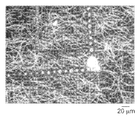
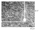
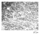
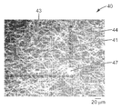
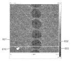
도 3a 내지 도 3d는 레이저 트레이스를 나타내는, 본 명세서에 기재된 투명 전극의 현미경 가시광 이미지이고;
<도 4a 내지 도 4d>
도 4a 내지 도 4d는 레이저 트레이스를 나타내는, 본 명세서에 기재된 투명 전극의 현미경 가시광 이미지이고;
<도 5a 내지 도 5c>
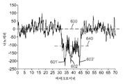
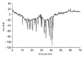
도 5a는 투명 전극의 예시적인 실시 형태에서의 레이저 트레이스의 원자력 현미경 이미지이고, 도 5b 및 도 5c는 도 5a의 레이저 트레이스의 프로파일 분석 결과이고;
<도 6a 및 도 6b>
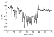
도 6a는 투명 전극의 예시적인 실시 형태에서의 레이저 트레이스의 원자력 현미경 이미지이고, 도 6b는 도 6a의 레이저 트레이스의 프로파일 분석 결과이고;
<도 7a 및 도 7b>
도 7a는 투명 전극의 예시적인 실시 형태에서의 레이저 트레이스의 원자력 현미경 이미지이고, 도 7b는 도 7a의 레이저 트레이스의 프로파일 분석 결과이고;
<도 8a 및 도 8b>
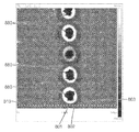
도 8a는 투명 전극의 예시적인 실시 형태에서의 레이저 트레이스의 원자력 현미경 이미지이고, 도 8b는 도 8a의 레이저 트레이스의 프로파일 분석 결과이고;
<도 9a 및 도 9b>
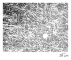
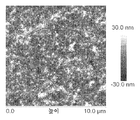
도 9a 및 도 9b는 조사되지 않은 필름 샘플의 원자력 현미경 이미지이고;
<도 10a 및 도 10b>
도 10a는 투명 전극의 예시적인 실시 형태에서의 레이저 트레이스의 원자력 현미경 이미지이고, 도 10b는 도 10a의 레이저 트레이스의 프로파일 분석 결과이고;
<도 11>
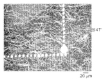
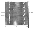
도 11은 투명 전극의 예시적인 실시 형태에서의 레이저 트레이스의 암시야 가시광 현미경 사진(darkfield visible micrograph)이고;
<도 12a 및 도 12b>
도 12a는 투명 전극의 예시적인 실시 형태에서의 레이저 트레이스의 원자력 현미경 이미지이고, 도 12b는 도 12a의 레이저 트레이스의 프로파일 분석 결과이고;
<도 13>
도 13은 투명 전극의 예시적인 실시 형태에 대한 흡광 스펙트럼이고;
<도 14a 및 도 14b>
도 14a 및 도 14b는 각각 ITO PET 필름 상의 레이저 트레이스의 원자력 현미경 이미지 및 프로파일 분석 결과이고;
<도 15>
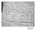
도 15는 투명 전도성 필름 샘플에서의 레이저 트레이스의 200X 배율에서의 가시광 현미경 사진이다.≪ 1 >
1 shows a cross-sectional view of a conductive portion of an exemplary embodiment of a transparent electrode described herein;
2,
Figure 2 is an ideal profile drawing of an insulating trace in the patterned transparent electrode described herein;
3A to 3D,
Figures 3a-3d are microscope visible light images of the transparent electrode described herein, illustrating laser traces;
4A to 4D,
Figures 4A-4D are microscope visible light images of the transparent electrode described herein, illustrating laser traces;
5A to 5C,
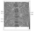
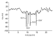
Figure 5A is an atomic force microscope image of a laser trace in an exemplary embodiment of a transparent electrode, Figures 5B and 5C are results of profile analysis of the laser trace of Figure 5A;
6A and 6B,
Figure 6a is an atomic force microscope image of a laser trace in an exemplary embodiment of a transparent electrode, Figure 6b is a profile analysis result of the laser trace of Figure 6a;
7A and 7B,
Figure 7a is an atomic force microscope image of a laser trace in an exemplary embodiment of a transparent electrode, Figure 7b is a profile analysis result of the laser trace of Figure 7a;
8A and 8B,
Figure 8a is an atomic force microscope image of a laser trace in an exemplary embodiment of a transparent electrode, Figure 8b is a profile analysis result of the laser trace of Figure 8a;
9A and 9B,
Figures 9A and 9B are atomic force microscope images of unexposed film samples;
10A and 10B,
10A is an atomic force microscope image of a laser trace in an exemplary embodiment of a transparent electrode, FIG. 10B is a profile analysis result of the laser trace of FIG. 10A; FIG.
11)
Figure 11 is a darkfield visible micrograph of a laser trace in an exemplary embodiment of a transparent electrode;
12A and 12B,
12A is an atomic force microscope image of a laser trace in an exemplary embodiment of a transparent electrode, FIG. 12B is a profile analysis result of the laser trace of FIG. 12A; FIG.
13,
Figure 13 is an absorption spectrum for an exemplary embodiment of a transparent electrode;
14A and 14B,
14A and 14B are the results of nuclear microscope image and profile analysis of laser traces on ITO PET films, respectively;
<Fig. 15>
15 is a visible light micrograph of a laser trace at 200X magnification in a transparent conductive film sample.
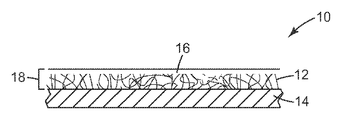
도 1은 본 발명의 투명 전극(10)(즉, 투명 전기 전도체)의 예시적인 실시 형태의 단면도를 나타내는데, 이는 투명 전극의 복수의 전기 전도성 영역 중 하나를 나타낸다. 투명 전극(10)은 투명 기판(14)의 주 표면의 적어도 일부분 상에 배치된 상호연결 금속성 나노와이어의 전기 전도성 층(12)을 포함하며, 중합체 오버코트 층(16)이 전기 전도성 층(12) 상에 배치된다. 중합체 오버코트 층(16) 및 전기 전도성 층(12)은 함께 복합층(18)(즉, 중합체 나노와이어 층)을 형성한다. 복수의 전기 전도성 영역을 분리하는 전기 절연성 트레이스는 도 1에 나타나있지 않다.Figure 1 shows a cross-sectional view of an exemplary embodiment of a transparent electrode 10 (i.e., a transparent electrical conductor) of the present invention, which represents one of a plurality of electrically conductive regions of a transparent electrode. The
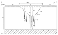
도 2는 본 발명의 패턴화된 투명 전기 전도체(20)(즉, 투명 전극)의 이상적인 프로파일 도인데, 이는, 예를 들어, 도 5b, 도 5c, 도 6b, 도 7b, 도 8b, 도 10b 및 도 12b에 도시된 원자력 현미경("AFM"; AFM은 실시예 섹션에서 더욱 상세하게 기술됨) 프로파일 데이터의 태양들을 설명하기 위해 전기 절연성 트레이스(21)의 태양들을 나타낸다. 투명 전기 전도체(20)의 이상적인 프로파일 도면은 복합층(28)의 x-y 평면의 x-축 및 y-축(복합층(28)의 상호연결 금속성 나노와이어는 도시되지 않음) 및 복합층(28)의 x-y 평면 내로의 z-축에 대해 배향된다. 전기 절연성 트레이스(21)는 전기 전도성 영역들(24, 24')을 분리하는 밸리(26)를 형성하며, 밸리(26)는 최대 깊이(27) 및 단면 폭(M1)을 갖는다. 전기 절연성 트레이스(21)는 복합층(28)의 x-y 평면의 z-축 내로 추가로 깊이(23)를 갖는 복수의 크레비스(22)를 추가로 포함한다. 도 2에 나타낸 실시 형태는 z-축을 따라 단지 복합층(28) 내에서만 연장하는 밸리(26) 및 복수의 크레비스(22)를 나타내지만, (도시되지 않은) 일부 실시 형태에서 복수의 크레비스(22)는 z-축을 따라 투명 기판(201) 내로 연장할 수 있다. (도시되지 않은) 일부 실시 형태에서, 밸리(26)의 최대 깊이(27)는 z-축을 따라 투명 기판(201) 내로 연장할 수 있다.Figure 2 is an ideal profile of a patterned transparent electrical conductor 20 (i.e., a transparent electrode) of the present invention, which may include, for example, Figures 5b, 5c, 6b, 7b, 8b, 10b And the atomic force microscope ("AFM" shown in FIG. 12B; AFM is described in more detail in the embodiment section) profile data. The ideal profile of the transparent
전형적으로 본 발명의 전기 절연성 레이저 트레이스는 이들 절연성 레이저 트레이스의 단면 분석에 있어서 2가지 수준의 구조를 갖는다: 레이저 빔의 폭에 거의 상응하는 폭을 가지며 코팅 및 레이저 출력에 따라 10 nm 미만으로부터 100 nm 초과에 이르는 범위일 수 있는 깊이를 갖는 넓은 주 밸리(primary valley; 즉, 트렌치(trench))에, 최대 50 내지 100 nm의 깊이를 갖는 은 나노와이어의 형상으로 상대적으로 예리한 크레비스가 겹쳐져 있다.Typically, the electrically insulative laser traces of the present invention have two levels of structure in the cross-section analysis of these insulative laser traces: with a width approximately corresponding to the width of the laser beam and from less than 10 nm to 100 nm A relatively sharp crevice is superimposed on a wide primary valley (i.e., a trench) having a depth that can be in the range of more than 50 nanometers, with a depth of silver nanowires of up to 50 to 100 nm.
본 발명의 전기 절연성 레이저 트레이스의 실시 형태는 이상적인 것으로부터 벗어나는 특징부를 가질 수 있다. 예를 들어, 일부 실시 형태에서, 레이저 트레이스는 펄스형 레이저가 투명 전극을 통과한 곳에 위치된 일련의 스팟(spot)일 수 있다. 펄스형 레이저 트레이스의 AFM 이미지는 실시예 섹션(예를 들어, 도 5a, 도 6a, 도 7a, 도 8a, 도 10a 및 도 12a 참조)에서 볼 수 있는데, 이상적인 것으로부터의 다양한 정도로 벗어난 것이 관찰된다.Embodiments of the electrically insulative laser traces of the present invention may have features deviating from the ideal. For example, in some embodiments, the laser traces may be a series of spots located where the pulsed laser passes through the transparent electrode. The AFM image of the pulsed laser traces can be seen in the example section (see, for example, Figures 5A, 6A, 7A, 8A, 10A and 12A) .
일부 실시 형태에서, 본 발명의 투명 전극(20)은 광학적으로 투명하다. 투명 전극(20)은, 전기 전도성 특성의 손실 없이 휘어져서, 만곡된 표면에 순응하는(conformable) 디스플레이를 제공할 수 있도록 가요성일 수 있다.In some embodiments, the
본 발명의 투명 전극의 전기 전도성 영역은, 전기 전도성 (약 104 ohm/sq 미만의 시트 저항)이며 전자기 스펙트럼의 적어도 일부분의 방사선을 투과하는 스트립, 평면 또는 표면을 갖는 투명 기판을 포함한다. 특히, 투명 전극은, 투명 기판과, 투명 기판 상에 배치되며 금속성 나노와이어를 포함하는 전도성 층, 전도성 층 상에 배치되며 안티몬 주석 산화물, 아연 산화물 및 인듐 주석 산화물로 이루어진 군으로부터 선택되는 나노입자를 선택적으로 포함하는 중합체 오버코트 층을 포함하고, 여기서 전도성 층 없이 투명 기판 상에 배치된 중합체 오버코트 층의 시트 저항은 약 107 ohm/sq 초과이다.Electrically conductive regions of the transparent electrode of the present invention, the electrical conductivity (sheet resistance of about less than 10 4 ohm / sq) comprises a transparent substrate having at least a portion of the radiation which passes through the strip, the plane or surface of the electromagnetic spectrum. In particular, the transparent electrode comprises a transparent substrate, a conductive layer disposed on the transparent substrate and comprising a metallic nanowire, a nanoparticle disposed on the conductive layer and selected from the group consisting of antimony tin oxide, zinc oxide, and indium tin oxide Optionally comprising a polymeric overcoat layer, wherein the sheet resistivity of the polymeric overcoat layer disposed on the transparent substrate without a conductive layer is greater than about 10 7 ohm / sq.
투명 전극은, 광학 성능이, 낮은 탁도 및 높은 가시광 투과율을 필요로 하는 디스플레이 응용에서 사용될 수 있다. 예를 들어, 그러한 디스플레이는, (a) 투명 전극을 포함하는 제1 전극 - 투명 기판은 제1 기판을 포함함 -; (b) 제2 기판; 및 (c) 중합체 오버코트 층과 제2 기판 사이에 배치되는 이미지 형성 재료를 포함한다. 일부 실시 형태에서, 제2 기판은 투명하다. 일부 실시 형태에서, 제2 기판은 불투명하다. 투명 전극이 사용될 수 있는 예시적인 디스플레이에는, 중합체 분산형(polymer-dispersed) 액정 디스플레이, 액정 디스플레이, 전기영동 디스플레이, 전기변색(electrochromic) 디스플레이, 전계발광(electroluminescent) 디스플레이 및 플라즈마 디스플레이가 포함된다.Transparent electrodes can be used in display applications where optical performance requires low turbidity and high visible light transmittance. For example, such a display may comprise: (a) a first electrode comprising a transparent electrode, the transparent substrate comprising a first substrate; (b) a second substrate; And (c) an image forming material disposed between the polymer overcoat layer and the second substrate. In some embodiments, the second substrate is transparent. In some embodiments, the second substrate is opaque. Exemplary displays in which transparent electrodes can be used include polymer-dispersed liquid crystal displays, liquid crystal displays, electrophoretic displays, electrochromic displays, electroluminescent displays, and plasma displays.
전도성 재료로서 은을 이용하여 제조되는 투명 전극이 알려져 있다. 국제특허 공개 WO 2008/046058호 (알레만드(Allemand) 등)에 기재된 바와 같이, 은은, 은 나노와이어, 메시 또는 라인의 형태로 이용될 때 투명 전도성 재료로서 이용될 수 있다. 은 코팅은 높은 가시광 투과율 및 낮은 탁도와 함께 우수한 전도도를 제공하지만, 일부 응용에서, 특히 나노와이어 형태의, 은의 산화적 및 화학적 불안정성은, 은 층을 위한 보호 오버코트의 사용을 필요로 할 수 있다. 보호 오버코트는 은의 전도도 손실을 야기할 수 있는 기계적 손상 및 환경적 열화로부터 은을 보호할 수 있다.Transparent electrodes made using silver as a conductive material are known. As described in International Patent Publication No. WO 2008/046058 (Allemand et al.), Silver can be used as a transparent conductive material when used in the form of silver nanowires, meshes or lines. While silver coatings provide good conductivity with high visible light transmittance and low turbidity, the oxidative and chemical instability of silver in some applications, particularly in the form of nanowires, may require the use of a protective overcoat for the silver layer. Protective overcoats can protect silver from mechanical damage and environmental degradation that can lead to loss of conductivity of silver.
은을 위한 보호 오버코트에는 전기 절연 특성을 갖는 오버코트가 포함된다. 보호 오버코트는, 은 나노와이어 없이, 기판 상의 보호 오버코트의 코팅이 약 1012 ohm/sq 초과의 시트 저항을 갖는 경우에 전기 절연 특성을 갖는 것으로 간주된다. UV-경화성 아크릴 수지와 같은 재료는 절연 특성을 가지며 보호 오버코트를 제조하는 데에 특히 유용하다.Protective overcoats for silver include overcoats with electrical insulation properties. The protective overcoat is considered to have electrical insulation properties when the coating of the protective overcoat on the substrate has a sheet resistance of greater than about 10 12 ohm / sq, without silver nanowires. Materials such as UV-curable acrylic resins have insulating properties and are particularly useful for making protective overcoats.
은을 위한 보호 오버코트에는 전도 특성을 갖는 오버코트가 포함된다. 보호 오버코트는, 은 나노와이어 없이, 기판 상의 보호 오버코트의 코팅이 약 104 ohm/sq 미만의 시트 저항을 갖는 경우에 전도 특성을 갖는 것으로 간주된다. 전도 특성을 갖는 보호 오버코트를 제조하는 데 유용한 재료에는 ITO를 포함하는 다양한 유형의 진공-적용된 코팅이 포함되나, 이러한 접근법은 상기에 기재된 이유들로 인해 ITO 그 자체에 대해서는 유익하지 않다. 전도성 보호 오버코트는 또한 전도성 중합체를 포함할 수 있으나, 이 재료는 가시 영역에서 강하게 흡광한다. 예를 들어, 폴리(3,4-에틸렌다이옥시티오펜) 폴리(스티렌 설포네이트)(종종 PEDOT/PSS로 지칭됨)가 널리 사용되나, 이것은 남색(deep blue)이다. 전도성 중합체, 예를 들어, PEDOT/PSS, 다른 폴리티오펜, 및 폴리아닐린이 또한, 최대 109 ohm/sq의 오버코트 시트 저항을 제공하도록 적용되는 오버코트로서 사용될 수 있다. 그러한 오버코트는 OLED 디바이스 구조물에서 특히 유용하다.A protective overcoat for silver includes an overcoat having conductive properties. The protective overcoat is deemed to have conducting properties when the coating of the protective overcoat on the substrate has a sheet resistance of less than about 10 4 ohm / sq, without silver nanowires. Materials useful for making protective overcoats with conductive properties include various types of vacuum-applied coatings including ITO, but this approach is not beneficial for ITO itself due to the reasons described above. The conductive protective overcoat may also comprise a conductive polymer, but the material strongly absorbs in the visible region. For example, poly (3,4-ethylenedioxythiophene) poly (styrenesulfonate) (sometimes referred to as PEDOT / PSS) is widely used, but it is deep blue. Conducting polymers such as PEDOT / PSS, other polythiophenes, and polyanilines may also be used as overcoats applied to provide an overcoat sheet resistance of up to 10 9 ohm / sq. Such an overcoat is particularly useful in OLED device constructions.
일부 실시 형태에서, 투명 전극은 탁도를 거의 또는 전혀 나타내지 않는데, 이는 투명 전극이 약 10% 이하(일부 실시 형태에서, 약 5% 이하, 또는 심지어 약 2% 이하)의 탁도 값을 가질 수 있음을 의미한다. 투명 전극 상에 수직으로 입사되는 광의 경우, 탁도 값은 총 투과광 강도에 대해, 수직 방향으로부터 4도 초과만큼 벗어난 투과광 강도의 비(ratio)이다. 본 명세서에 개시된 탁도 값은 ASTM D1003에 기재된 절차에 따라 탁도계(미국 메릴랜드주 실버 스프링 소재의 비와이케이-가드너(BYK-Gardiner)로부터 상표명 "헤이즈-가드 플러스"(HAZE-GARD PLUS)로 입수가능함)를 사용하여 측정하였다.In some embodiments, the transparent electrode exhibits little or no turbidity, indicating that the transparent electrode may have a turbidity value of about 10% or less (in some embodiments, about 5% or less, or even about 2% or less) it means. In the case of light vertically incident on the transparent electrode, the turbidity value is the ratio of the transmitted light intensity deviated by more than 4 degrees from the vertical direction with respect to the total transmitted light intensity. The turbidity values disclosed herein are measured using a turbidimeter (available under the trade designation "HAZE-GARD PLUS " from BYK-Gardiner, Silver Spring, MD) according to the procedure described in ASTM D1003. .
일부 실시 형태에서, 투명 전극은 가시광 스펙트럼(약 400 내지 약 700 nm)의 적어도 일부분에 걸쳐 약 80% 내지 약 100% (일부 실시 형태에서, 약 90% 내지 약 100%, 약 95% 내지 약 100%, 또는 심지어 약 98% 내지 약 100%)의 높은 광 투과율을 갖는다. 일부 실시 형태에서, 투명 전극은 가시광 스펙트럼 (약 400 내지 약 700 nm)의 적어도 일부분에 걸쳐 약 80% 이상, 약 90% 내지 약 100%, 또는 약 90% 내지 약 95%의 높은 광 투과율, 및 약 0.01% 내지 약 5% 미만의 탁도 값을 갖는다.In some embodiments, the transparent electrode is between about 80% and about 100% (in some embodiments from about 90% to about 100%, from about 95% to about 100% in some embodiments) over at least a portion of the visible light spectrum %, Or even from about 98% to about 100%). In some embodiments, the transparent electrode has a high light transmittance of at least about 80%, from about 90% to about 100%, or from about 90% to about 95% over at least a portion of the visible light spectrum (about 400 to about 700 nm) And has a turbidity value of from about 0.01% to less than about 5%.
전도성 층은 종횡비(aspect ratio)가 약 10 초과인 금속성 나노와이어를 포함하는데, 종횡비는 입자의 길이를 그의 직경으로 나누어 결정된다. 본 명세서에 사용되는 바와 같이, 금속성 나노와이어는 금속, 금속 합금, 또는 금속 산화물을 포함하는 금속 화합물을 포함하는 금속성 와이어를 지칭한다. 금속성 나노와이어의 적어도 하나의 단면 치수는 500 nm 미만 (일부 실시 형태에서, 200 nm 미만 또는 심지어 100 nm 미만)이다. 종횡비는 약 10 초과, 약 50 초과, 약 100 초과, 또는 약 10 내지 약 100,000이다. 금속성 나노와이어는 은, 금, 구리, 니켈, 및 금-도금된(gold-plated) 은을 포함하는 임의의 금속을 포함할 수 있다. 일 실시 형태에서, 금속성 나노와이어는, 예를 들어 국제특허 공개 WO 2008/046058호 (알레만드 등)에 기재된 것과 같은 은 나노와이어를 포함한다. 은 나노와이어는 국제특허 공개 WO 2008/046058호에 기재된 바와 같이 제조할 수 있거나 또는 상업적 공급처 (예를 들어, 미국 노스캐롤라이나주 샬롯 소재의 블루 나노(Blue Nano); 미국 캘리포니아주 라 졸라 소재의 씨쉘(Seashell); 및 미국 샌프란시스코 소재의 나노갭 유에스에이(Nanogap USA))로부터 입수할 수 있다.The conductive layer comprises metallic nanowires having aspect ratios greater than about 10, wherein the aspect ratio is determined by dividing the length of the particle by its diameter. As used herein, metallic nanowires refer to metallic wires comprising metal compounds, metal alloys, or metal compounds comprising metal oxides. At least one cross-sectional dimension of the metallic nanowire is less than 500 nm (in some embodiments, less than 200 nm or even less than 100 nm). The aspect ratio is greater than about 10, greater than about 50, greater than about 100, or from about 10 to about 100,000. The metallic nanowires may include any metal including silver, gold, copper, nickel, and gold-plated silver. In one embodiment, the metallic nanowires include silver nanowires such as those described, for example, in International Patent Publication No. WO 2008/046058 (Alleman et al.). Silver nanowires may be prepared as described in International Patent Publication No. WO 2008/046058 or may be prepared from commercially available sources such as Blue Nano, Charlotte, (Seashell), and Nanogap USA, San Francisco, USA.
금속성 나노와이어는 투명 기판의 표면 상에 전도성 네트워크를 형성한다. 일반적으로, 소정 용매 중 금속성 나노와이어의 분산액을 제조하고 투명 기판 상에 코팅한 후에, 코팅을 건조하여 용매를 제거한다. 금속성 나노와이어와 함께 안정한 분산액을 형성하는 임의의 용매, 예를 들어, 물, 알코올, 케톤, 에테르, 탄화수소, 방향족 탄화수소, 및 이들의 상용성(compatible) 혼합물이 사용될 수 있다. 금속성 나노와이어를 포함하는 분산액은, 코팅 제형에 전형적으로 사용되는 첨가제 (예를 들어, 계면활성제, 결합제, 점도 조절을 위한 재료, 및 부식 억제제)를 포함할 수 있다. 분산액 제형의 최적화와 코팅 및 건조 조건은 국제특허 공개 WO 2008/046058호 (알레만드 등)에 기재되어 있다.The metallic nanowires form a conductive network on the surface of the transparent substrate. Generally, after a dispersion of metallic nanowires in a given solvent is prepared and coated on a transparent substrate, the coating is dried to remove the solvent. Any solvent that forms a stable dispersion with the metallic nanowires may be used, for example, water, alcohols, ketones, ethers, hydrocarbons, aromatic hydrocarbons, and compatible mixtures thereof. Dispersions comprising metallic nanowires may include additives typically used in coating formulations (e.g., surfactants, binders, materials for viscosity control, and corrosion inhibitors). Optimization of the dispersion formulation and coating and drying conditions are described in International Patent Publication No. WO 2008/046058 (Alleman et al.).
일반적으로, 전도성 층의 두께는 사용되는 특정 금속성 나노와이어, 중합체 오버코트 층의 특성, 및 이미징(imaging) 재료에 따라 좌우된다. 대부분의 경우에, 디스플레이의 성능에 대한 임의의 악영향 및 비용을 최소화하기 위하여, 사용되는 금속성 나노와이어의 양을 최소화하는 것이 바람직하다. 전도성 층은 금속성 나노와이어에 부가하여 다양한 성분을 포함할 수 있다. 일 실시 형태에서, 전도성 층은 금속성 나노와이어로 본질적으로 이루어진다. 다른 실시 형태에서, 전도성 층은 약 40 중량% 초과의 금속성 나노와이어를 포함하는데, 나머지 중량%는 결합제 및 계면활성제와 같은 첨가제로 구성된다.In general, the thickness of the conductive layer will depend on the particular metallic nanowire used, the nature of the polymeric overcoat layer, and the imaging material. In most cases, it is desirable to minimize the amount of metallic nanowires used to minimize any adverse effects and costs on the performance of the display. The conductive layer may comprise various components in addition to the metallic nanowires. In one embodiment, the conductive layer consists essentially of a metallic nanowire. In another embodiment, the conductive layer comprises greater than about 40 weight percent metallic nanowires, with the balance weight percent consisting of additives such as a binder and a surfactant.
전도성 층의 두께는 전형적으로 약 500 nm 미만이다. 일부 실시 형태에서, 전도성 층은 나노와이어의 메시 또는 네트워크의 형태이거나 또는 투명 기판의 표면에 걸쳐 다소 불연속적인 형태이다. 일부 실시 형태에서, 금속성 나노와이어는, 투명 전도성 영역과 투명 비-전도성 영역을 포함하는 패턴을 형성하도록, 투명 기판 상에 배치된다. 예시적인 패턴은 라인들의 어레이, 또는 약 5 마이크로미터 내지 약 500 마이크로미터 이상만큼 서로 이격된, 이산된(discrete) 전도성 영역들을 포함한다.The thickness of the conductive layer is typically less than about 500 nm. In some embodiments, the conductive layer is in the form of a mesh or network of nanowires or somewhat discontinuous over the surface of the transparent substrate. In some embodiments, the metallic nanowires are disposed on a transparent substrate to form a pattern comprising a transparent conductive region and a transparent non-conductive region. An exemplary pattern includes an array of lines, or discrete conductive regions spaced from each other by at least about 5 micrometers to about 500 micrometers or more.
전형적으로, 사용되는 특정 금속성 나노와이어 및 전도성 층의 두께는, 투명 기판 상에 배치되는 층의 요구되는 시트 저항에 의해 결정된다. 시트 저항의 전형적인 범위는 약 10 ohm/sq 내지 약 5000 ohm/sq인데, 바람직한 범위는 특정 디바이스 및 응용에 따라 좌우된다. 유기 발광 다이오드(OLED) 디바이스의 경우, 전형적인 시트 저항은 약 10 내지 약 50 ohm/sq이며; PLDC 및 콜레스테릭 액정 디바이스의 경우, 전형적인 시트 저항은 약 50 내지 약 250 ohm/sq이고; 전기영동 디스플레이 디바이스의 경우, 전형적인 시트 저항은 약 50 내지 약 2000 ohm/sq이다.Typically, the thickness of the particular metallic nanowire and conductive layer used is determined by the sheet resistance required of the layer disposed on the transparent substrate. A typical range of sheet resistance is from about 10 ohm / sq to about 5000 ohm / sq, the preferred range depending on the particular device and application. For organic light emitting diode (OLED) devices, typical sheet resistance is about 10 to about 50 ohm / sq; For PLDC and cholesteric liquid crystal devices, typical sheet resistance is about 50 to about 250 ohm / sq; For electrophoretic display devices, typical sheet resistance is from about 50 to about 2000 ohm / sq.
전도성 층의 시트 저항은 접촉(contact) 방법 및 비-접촉(non-contact) 방법에 의해 측정될 수 있다. 접촉 방법에서는, 전압계에 연결된 두 개의 금속 접점을 포함하는 2점 탐침을, 탐침이 층과 접촉하도록, 전도성 층 상에 배치한다. 비-접촉 방법에서는, 무접점 탐침을 갖는 장비(예를 들어, 미국 위스콘신주 프레스컷 소재의 델콤 프로덕츠, 인크.(Delcom Products Inc.)로부터 상표명 "델콤 717B 논-콘택트 컨덕턴스 모니터"(DELCOM 717B NON-CONTACT CONDUCTANCE MONITOR)로 입수가능한 장비)를 사용할 수 있다.The sheet resistance of the conductive layer can be measured by a contact method and a non-contact method. In the contact method, a two-point probe comprising two metal contacts connected to a voltmeter is placed on the conductive layer such that the probe is in contact with the layer. In a non-contact method, a device with a contactless probe (e.g., DELCOM 717B NON (trade name) from Delcom Products Inc., Prescott, Wisconsin, -CONTACT CONDUCTANCE MONITOR) can be used.
투명 전극은 하기에서 기재된 바와 같이 상이한 유형의 디스플레이들에서 사용될 수 있다. 일부 디스플레이에서, 투명 전극은 광이 전극을 통해 투과되어 관찰자(viewer)를 향하도록 설계될 필요가 있다. 이러한 경우에, 전도성 층의 성분 및 두께는, 층의 광학 특성이 특정 요건을 충족시키도록 선택될 필요가 있다.Transparent electrodes can be used in different types of displays as described below. In some displays, the transparent electrode needs to be designed so that light is transmitted through the electrodes and directed toward the viewer. In this case, the composition and thickness of the conductive layer need to be selected such that the optical properties of the layer meet certain requirements.
금속성 나노와이어가 부식 및 마모와 같은 부정적인 환경적 요인으로부터 보호되도록, 중합체 오버코트 층이 전도성 층 상에 배치된다. 구체적으로, 중합체 오버코트 층은 수분(moisture), 미량(trace amount)의 산, 산소, 및 황과 같은 부식성 요소들의 투과성(permeability)을 방지하거나 적어도 최소화하도록 설계될 수 있다.A polymeric overcoat layer is disposed on the conductive layer such that the metallic nanowires are protected from negative environmental factors such as corrosion and abrasion. Specifically, the polymeric overcoat layer can be designed to prevent, or at least minimize, the permeability of corrosive elements such as moisture, trace amounts of acid, oxygen, and sulfur.
일반적으로, 중합체 오버코트 층은 예비-중합(pre-polymerize)되거나 되지 않을 수 있는 유기 성분으로부터 형성된다. 유기 성분은, 중합체 오버코트 층이 전도성 층 상에 형성될 수 있고 전도성 층이 부식 및 마모로부터 보호되지만 생성되는 디스플레이에서 요구되는 대로 기능할 수 있는 한 특별히 제한되지 않다.Generally, the polymeric overcoat layer is formed from organic components that may or may not be pre-polymerized. The organic component is not particularly limited as long as the polymeric overcoat layer can be formed on the conductive layer and the conductive layer is protected from corrosion and abrasion, but can function as required in the resulting display.
일부 실시 형태에서, 중합체 오버코트 층은, 분자량이 약 500 g/mol 미만인 소분자, 분자량이 500 g/mol 초과 내지 약 10,000 g/mol인 올리고머, 및 분자량이 10,000 g/mol 초과 내지 약 100,000 g/mol인 중합체를 포함할 수 있는 단량체와 같은 하나 이상의 중합성 성분을 포함하는 중합성 제형으로부터 형성된다. 중합성 단량체 또는 올리고머는 화학 방사선 (예를 들어, 가시광, 자외 방사선, 전자 빔 방사선, 열 및 그 조합), 또는 광화학적으로, 열적으로, 또는 산화환원적으로(redox) 개시될 수 있는 임의의 다양한 통상적인 음이온, 양이온, 자유 라디칼 또는 기타 중합 기술을 사용하여 경화될 수 있다.In some embodiments, the polymeric overcoat layer comprises a small molecule having a molecular weight less than about 500 g / mol, an oligomer having a molecular weight greater than 500 g / mol to about 10,000 g / mol, and a molecular weight greater than 10,000 g / mol to about 100,000 g / mol Such as a monomer capable of containing at least one polymerizable component. Polymerizable monomers or oligomers can be prepared by any method known in the art, including, but not limited to, actinic radiation (e.g., visible light, ultraviolet radiation, electron beam radiation, heat and combinations thereof), or any photochemically, thermally, Can be cured using various conventional anions, cations, free radicals, or other polymerization techniques.
중합체 오버코트 층을 형성하기에 적합한 중합성 기의 대표적인 예에는 에폭시 기, 에틸렌계 불포화 기, 알릴옥시 기, (메트)아크릴레이트 기, (메트)아크릴아미드 기, 시아노에스테르 기, 비닐 에테르 기, 및 그 조합이 포함된다. 단량체는 1작용성 또는 다작용성일 수 있으며, 중합 시에 가교결합된 네트워크를 형성하는 것이 가능할 수 있다. 본 명세서에 사용되는 바와 같이, (메트)아크릴레이트는 아크릴레이트 및 메타크릴레이트를 지칭하며, (메트)아크릴아미드는 아크릴아미드 및 메타크릴아미드를 지칭한다.Representative examples of polymerizable groups suitable for forming the polymeric overcoat layer include epoxy groups, ethylenically unsaturated groups, allyloxy groups, (meth) acrylate groups, (meth) acrylamide groups, cyanoester groups, vinyl ether groups, And combinations thereof. The monomers may be monofunctional or polyfunctional and may be capable of forming a crosslinked network upon polymerization. As used herein, (meth) acrylate refers to acrylate and methacrylate, and (meth) acrylamide refers to acrylamide and methacrylamide.
유용한 1작용성 단량체에는 스티렌, 알파-메틸스티렌, 치환된 스티렌, 비닐 에스테르, 비닐 에테르, N-비닐-2-피롤리돈, (메트)아크릴아미드, N-치환된 (메트)아크릴아미드, 옥틸 (메트)아크릴레이트, 아이소-옥틸 (메트)아크릴레이트, 노닐페놀 에톡실레이트 (메트)아크릴레이트, 아이소노닐 (메트)아크릴레이트, 다이에틸렌 글리콜 모노(메트)아크릴레이트, 아이소보르닐 (메트)아크릴레이트, 2-(2-에톡시에톡시)에틸 (메트)아크릴레이트, 2-에틸헥실 (메트)아크릴레이트, 라우릴 (메트)아크릴레이트, 부탄다이올 모노(메트)아크릴레이트, 베타-카르복시에틸 (메트)아크릴레이트, 아이소부틸 (메트)아크릴레이트, 지환족 에폭사이드, 2-하이드록시에틸 (메트)아크릴레이트, (메트)아크릴로니트릴, 말레산 무수물, 이타콘산, 아이소데실 (메트)아크릴레이트, 도데실 (메트)아크릴레이트, n-부틸 (메트)아크릴레이트, 메틸 (메트)아크릴레이트, 헥실 (메트)아크릴레이트, (메트)아크릴산, N-비닐카프로락탐, 스테아릴 (메트)아크릴레이트, 하이드록실 작용성 폴리카프로락톤 에스테르 (메트)아크릴레이트, 하이드록시프로필 (메트)아크릴레이트, 하이드록시아이소프로필 (메트)아크릴레이트, 하이드록시부틸 (메트)아크릴레이트, 하이드록시아이소부틸 (메트)아크릴레이트, 테트라하이드로푸르푸릴 (메트)아크릴레이트, 및 그 조합이 포함된다.Useful monofunctional monomers include styrene, alpha-methylstyrene, substituted styrenes, vinyl esters, vinyl ethers, N-vinyl-2-pyrrolidone, (meth) acrylamide, N-substituted (meth) (Meth) acrylate, iso-octyl (meth) acrylate, nonylphenol ethoxylate (meth) acrylate, isononyl (meth) acrylate, diethylene glycol mono Acrylate, lauryl (meth) acrylate, butanediol mono (meth) acrylate, beta (2-ethoxyethoxy) (Meth) acrylate, (meth) acrylonitrile, maleic anhydride, itaconic acid, isodecyl (meth) acrylate, isobutyl (meth) acrylate, Meth) acrylate, (Meth) acrylate, n-butyl (meth) acrylate, methyl (meth) acrylate, hexyl (meth) acrylate, (Meth) acrylate, hydroxypropyl (meth) acrylate, hydroxyisopropyl (meth) acrylate, hydroxybutyl (meth) acrylate, hydroxyisobutyl Tetrahydrofurfuryl (meth) acrylate, and combinations thereof.
내구성, 가요성, 전도성 층 및/또는 투명 기판에 대한 접착성, 내후성, 및 투과성을 제공하기 위하여, 중합성 올리고머 및 중합체를 포함하는 적합한 고분자량 성분이 중합체 오버코트 층 내에 포함될 수 있다. 이러한 고분자량 성분은 중합체 오버코트 층을 형성하기 위한 적합한 코팅 제형을 얻는 데에 또한 유용할 수 있으며, 예를 들어, 점도 제어를 제공하거나 경화 시 층의 수축을 감소시키는 데 사용될 수 있다. 올리고머 및/또는 중합체 자체는 직쇄형(straight-chained), 분지형(branched) 및/또는 환형(cyclic)일 수 있다. 분지형 올리고머 및/또는 중합체는 비슷한 분자량의 직쇄형 대응물보다 낮은 점도를 갖는 경향이 있다.Suitable high molecular weight components, including polymeric oligomers and polymers, may be included in the polymeric overcoat layer to provide durability, flexibility, conductive layer and / or adhesion, weatherability, and permeability to the transparent substrate. Such high molecular weight components may also be useful in obtaining suitable coating formulations for forming a polymeric overcoat layer and may be used, for example, to provide viscosity control or to reduce shrinkage of the layer upon curing. The oligomers and / or polymers themselves may be straight-chained, branched and / or cyclic. Branched oligomers and / or polymers tend to have lower viscosities than straight chain counterparts of similar molecular weight.
예시적인 중합성 올리고머 및 중합체에는 지방족 폴리우레탄, (메트)아크릴레이트, 폴리에스테르, 폴리이미드, 폴리아미드, 에폭시 중합체, 폴리스티렌(스티렌의 공중합체를 포함함) 및 치환된 스티렌, 실리콘-함유 중합체, 플루오르화된 중합체, 및 그 조합이 포함된다. 일부 응용에서, 폴리우레탄 (메트)아크릴레이트 올리고머 및/또는 중합체는 개선된 내구성 및 내후성 특징을 가질 수 있다. 이러한 재료는 또한 방사선 경화성 단량체, 특히 (메트)아크릴레이트 단량체로부터 형성되는 반응성 희석제에 용이하게 용해 가능한 경향이 있다. 예시적인 중합성 올리고머 및 중합체는, 우레탄 (메트)아크릴레이트, 에폭시 (메트)아크릴레이트, 폴리에스테르 (메트)아크릴레이트, 폴리에테르 (메트)아크릴레이트, (메트)아크릴화된 (메트)아크릴, (메트)아크릴화된 실리콘, 비닐 (메트)아크릴레이트, 및 (메트)아크릴화된 오일과 같은 상기에 기재된 작용기들의 조합을 포함한다.Exemplary polymerizable oligomers and polymers include but are not limited to aliphatic polyurethanes, (meth) acrylates, polyesters, polyimides, polyamides, epoxy polymers, polystyrenes including copolymers of styrene and substituted styrenes, Fluorinated polymers, and combinations thereof. In some applications, the polyurethane (meth) acrylate oligomer and / or polymer may have improved durability and weatherability characteristics. Such materials also tend to be readily soluble in radiation-curable monomers, particularly reactive diluents formed from (meth) acrylate monomers. Exemplary polymerizable oligomers and polymers include, but are not limited to, urethane (meth) acrylates, epoxy (meth) acrylates, polyester (meth) acrylates, polyether (meth) acrylates, (meth) (Meth) acrylated silicone, vinyl (meth) acrylate, and (meth) acrylated oils.
중합체 오버코트 층은 또한 중합 가능하지 않은 유기 성분으로부터 형성될 수 있으며, 특히, 일부 수성 및/또는 유기 용매-기반 제형 중의 다른 오버코트 성분들과 간단히 배합하고 전도성 층 위에 코팅한 후에 임의의 휘발성 물질을 제거하여 중합체 오버코트 층을 형성할 수 있는 중합체로부터 형성될 수 있다. 예시적인 중합체에는 폴리(메트)아크릴레이트, 폴리스티렌, 폴리우레탄, 폴리티오펜, 폴리아닐린, 폴리피롤, 폴리(비닐알코올) 공중합체 및 폴리에스테르가 포함된다.The polymeric overcoat layer can also be formed from non-polymerizable organic components, particularly when combined with other overcoat components in some aqueous and / or organic solvent-based formulations and coated on the conductive layer, then remove any volatiles Lt; / RTI > to form a polymeric overcoat layer. Exemplary polymers include poly (meth) acrylates, polystyrenes, polyurethanes, polythiophenes, polyanilines, polypyrroles, poly (vinyl alcohol) copolymers and polyesters.
1작용성 단량체의 특정 예에는 상기에 기재된 것들이 포함된다. 다작용성 단량체의 특정 예에는 펜타에리트리톨 트라이아크릴레이트 (미국 펜실베이니아주 엑스턴 소재의 사토머 컴퍼니(Sartomer Co.)로부터 상표명 "SR 444C"로 입수가능함), 헥산다이올 다이아크릴레이트, 우레탄 아크릴레이트 올리고머 (예를 들어, 사토머 컴퍼니로부터 상표명 "CN 981 B88"로, 그리고 미국 코네티컷주 월링포드 소재의 사이텍 인더스트리즈(Cytec Industries)로부터 상표명 "UCECOAT 7655" 및 "UCECOAT 7689"로 입수가능한 그러한 올리고머를 포함함)가 포함된다.Specific examples of monofunctional monomers include those described above. Specific examples of multifunctional monomers include pentaerythritol triacrylate (available under the trade designation "SR 444C" from Sartomer Co., Exton, Pennsylvania), hexanediol diacrylate, urethane acrylate UCECOAT 7655 " and "UCECOAT 7689" from Cytec Industries of Wallingford, Conn., Under the trade designations "CN 981 B88" ).
예비형성된(preformed) 중합체의 특정 예에는 폴리메틸메타크릴레이트 (루사이트 인터내셔널, 인크.(Lucite International, Inc.)로부터 상표명 "엘바사이트(ELVACITE) 2041"로 입수가능한 그러한 폴리메틸메타크릴레이트를 포함함), 폴리스티렌, 폴리티오펜 (미국 펜실베이니아주 피츠버그 소재의 플렉스트로닉스, 인크.(Plextronics, Inc.)로부터 상표명 "플렉스코어(PLEXCORE) OC RG-1100" 및 "플렉스코어 OC RG-1200"로 입수가능한 그러한 폴리티오펜을 포함함), 및 폴리비닐부티랄 (미국 미주리주 세인트루이스 소재의 솔루티아 인크.(Solutia Inc.)로부터 상표명 "BUTVAR"로 입수가능한 그러한 폴리비닐부티랄을 포함함)이 포함된다.Specific examples of preformed polymers include polymethylmethacrylate (such polymethylmethacrylate available from Lucite International, Inc. under the trade designation "ELVACITE 2041 " Available from Plextronics, Inc. under the trade designations "PLEXCORE OC RG-1100" and "Flexcore OC RG-1200", available from Plextronics, Inc., Pennsylvania, USA), polystyrene, polythiophene (Including such polythiophenes as possible), and polyvinyl butyral (including such polyvinyl butyral available under the trade designation "BUTVAR " from Solutia Inc., St. Louis, Mo.) do.
일부 실시 형태에서, 중합체 오버코트 층은 다작용성 (메트)아크릴레이트의 반응 생성물을 포함한다. 예를 들어, 중합체 오버코트 층은 메틸 (메트)아크릴레이트 중합체, 및 다작용성 (메트)아크릴레이트의 반응 생성물을 포함할 수 있다. 다른 예를 들면, 중합체 오버코트 층은 우레탄 (메트)아크릴레이트 올리고머 및 다작용성 (메트)아크릴레이트의 반응 생성물을 포함할 수 있다.In some embodiments, the polymeric overcoat layer comprises the reaction product of a multifunctional (meth) acrylate. For example, the polymeric overcoat layer may comprise the reaction product of a methyl (meth) acrylate polymer, and a polyfunctional (meth) acrylate. In another example, the polymeric overcoat layer may comprise the reaction product of a urethane (meth) acrylate oligomer and a polyfunctional (meth) acrylate.
중합체 오버코트 층은 또한, 직경이 약 500 nm 미만 (일부 실시 형태에서, 약 10 nm 내지 약 500 nm, 또는 심지어 약 40 nm 내지 약 200 nm)이며 안티몬 주석 산화물, 아연 산화물, 인듐 주석 산화물, 및 그 조합으로 이루어진 군으로부터 선택되는 나노입자를 포함할 수 있다. 이러한 금속 산화물 나노입자는 열수 합성 방법(hydrothermal synthetic method)에 의해 제조할 수 있거나 또는 상업적 공급처 (예를 들어, 대한민국 소재의 어드밴스드 나노 프로덕츠(Advanced Nano Products); 미국 일리노이주 데스 플레인스 소재의 석경 에이티 인크.(Su㎏yung AT Inc.); 및 미국 뉴저지주 파시파니 소재의 에보닉 데구사 코포레이션(Evonik Degussa Corp.))로부터 입수할 수 있다.The polymeric overcoat layer may also be comprised of antimony tin oxide, zinc oxide, indium tin oxide, and mixtures thereof, having a diameter of less than about 500 nm (in some embodiments, from about 10 nm to about 500 nm, or even from about 40 nm to about 200 nm) ≪ / RTI > and combinations thereof. These metal oxide nanoparticles can be made by the hydrothermal synthetic method or can be prepared from commercial sources (e.g., Advanced Nano Products, Inc., South Korea; And Evonik Degussa Corp., Parsippany, NJ, USA). ≪ / RTI >
중합체 오버코트 층은 층의 요구되는 특성 및 성능이 얻어지는 한, 유기 성분 및 나노입자를 임의의 상대량(relative amount)으로 포함한다. 일부 실시 형태에서, 유기 성분 대 나노입자의 중량 비는 약 85:15 내지 약 25:75, 및 심지어 일부 실시 형태에서 약 75:25 내지 약 40:60일 수 있다.The polymeric overcoat layer contains the organic component and the nanoparticles in any relative amount as long as the required properties and performance of the layer are obtained. In some embodiments, the weight ratio of organic component to nanoparticles can be from about 85:15 to about 25:75, and even in some embodiments, from about 75:25 to about 40:60.
중합체 오버코트 층의 두께는, 층이 금속성 나노와이어를 부식 및 마모로부터 보호하고 층의 요구되는 특성 및 성능이 얻어지는 한, 특별히 제한되지 않는다. 일부 실시 형태에서, 중합체 오버코트 층의 두께는 약 1 마이크로미터 미만, 및 심지어 일부 실시 형태에서 약 50 nm 내지 약 1 마이크로미터이다. 일부 예시적인 실시 형태에서, 중합체 오버코트 층은, 금속성 나노와이어의 일부분이 중합체 오버코트 층의 표면으로부터 돌출되어 전도성 층에 대한 액세스(access)가 가능해지도록, 전도성 층 상에 배치될 수 있다. 일부 실시 형태에서, 금속성 나노와이어는 중합체 오버코트 층의 표면으로부터 돌출되지 않으며, 전도성 층은 중합체 오버코트 내의 개구 또는 투명 전극의 에지에 있는 개구를 통해 액세스된다. 일부 실시 형태에서, 금속성 나노와이어는 중합체 층의 표면으로부터 돌출되지 않으며, 전도성 층은 중합체 오버코트 층의 얇은 부분을 통해 액세스된다.The thickness of the polymeric overcoat layer is not particularly limited as long as the layer protects the metallic nanowire from corrosion and abrasion and the required properties and performance of the layer are obtained. In some embodiments, the thickness of the polymeric overcoat layer is less than about 1 micrometer, and even in some embodiments, from about 50 nm to about 1 micrometer. In some exemplary embodiments, the polymeric overcoat layer can be disposed on the conductive layer such that a portion of the metallic nanowire protrudes from the surface of the polymeric overcoat layer to allow access to the conductive layer. In some embodiments, the metallic nanowires do not protrude from the surface of the polymeric overcoat layer, and the conductive layer is accessed through an opening in the polymeric overcoat or an edge in the transparent electrode. In some embodiments, the metallic nanowires do not protrude from the surface of the polymer layer, and the conductive layer is accessed through a thin portion of the polymeric overcoat layer.
일반적으로, 중합체 오버코트 층의 구체적인 성분 및 양, 층 두께 등은 많은 요인들, 예를 들어, 사용되는 유기 성분, 나노입자, 금속성 나노와이어의 화학적 성질, 전도성 층 내에 존재하는 금속성 나노와이어의 양, 전도성 층의 두께, 이미징 재료, 및 투명 전극이 사용되는 디스플레이의 유형에 따라 좌우될 것이다.In general, the specific ingredients and amounts of the polymeric overcoat layer, the thickness of the layer, and the like can be influenced by many factors, such as the chemical nature of the organic components, nanoparticles, metallic nanowires used, the amount of metallic nanowires present in the conductive layer, The thickness of the conductive layer, the imaging material, and the type of display on which the transparent electrode is to be used.
일부 실시 형태에서, 중합체 오버코트 층은, 가시광 스펙트럼 (약 400 nm 내지 약 700 nm)의 적어도 일부분에 걸쳐, 약 80% 내지 약 100% (일부 실시 형태에서, 약 90% 내지 약 100%, 약 95% 내지 약 100%, 또는 심지어 약 98% 내지 약 100%)의 높은 광 투과율을 갖는 광학적으로 깨끗한 층을 포함한다. 일부 실시 형태에서, 중합체 오버코트 층은 약 5% 미만 (일부 실시 형태에서, 약 3% 미만, 또는 심지어 약 1% 미만)의 탁도 값을 갖는다. 일부 실시 형태에서, 중합체 오버코트 층은 약 0.1 내지 약 5% 미만 (일부 실시 형태에서, 약 0.1 내지 약 3% 미만, 또는 심지어 약 0.1 내지 약 1% 미만)의 탁도 값을 갖는다.In some embodiments, the polymeric overcoat layer has a thickness of from about 80% to about 100% (in some embodiments from about 90% to about 100%, from about 95% to about 100%, in some embodiments) over at least a portion of the visible light spectrum % ≪ / RTI > to about 100%, or even from about 98% to about 100%). In some embodiments, the polymeric overcoat layer has a turbidity value of less than about 5% (in some embodiments, less than about 3%, or even less than about 1%). In some embodiments, the polymeric overcoat layer has a turbidity value of from about 0.1 to less than about 5% (in some embodiments, from about 0.1 to less than about 3%, or even from about 0.1 to less than about 1%).
중합체 오버코트 층은 층, 투명 전극, 및 투명 전극이 포함되는 디스플레이의 요구되는 특성에 따라 선택된다. 중합체 오버코트 층을 위한 코팅 제형을, 전도성 층 없이 투명 기판 상에 직접 코팅하고, 경화, 건조 등을 수행하여 중합체 오버코트 층을 형성한다. 이어서, 코팅된 투명 기판의 시트 저항을 측정함으로써 중합체 오버코트 층의 성능을 결정한다. 전도성 층 없이 투명 기판 상에 배치된 중합체 오버코트 층의 시트 저항은 약 107 ohm/sq 초과이어야 한다. 일부 실시 형태에서, 시트 저항은 약 107 ohm/sq 내지 약 1012 ohm/sq이다. 주어진 중합체 오버코트 층에 대해, 시트 저항은 층의 두께를 변경함으로써 달라질 수 있으며, 금속성 나노와이어가 부식 및 마모로부터 보호되는 한, 층은 요구되는 만큼 얇을 수 있다. 중합체 오버코트 층의 시트 저항은 상기에 기재된 것과 같은 접촉 방법 및 비-접촉 방법에 의해 측정될 수 있다.The polymeric overcoat layer is selected according to the desired properties of the display, including the layer, the transparent electrode, and the transparent electrode. The coating formulation for the polymeric overcoat layer is coated directly on the transparent substrate without a conductive layer, followed by curing, drying, etc. to form a polymeric overcoat layer. The performance of the polymeric overcoat layer is then determined by measuring the sheet resistance of the coated transparent substrate. The sheet resistance of the polymeric overcoat layer disposed on the transparent substrate without a conductive layer should be greater than about 10 7 ohm / sq. In some embodiments, the sheet resistance is from about 10 7 ohm / sq to about 10 12 ohm / sq. For a given polymeric overcoat layer, the sheet resistance can be varied by changing the thickness of the layer, and as long as the metallic nanowires are protected from corrosion and abrasion, the layer can be as thin as required. The sheet resistance of the polymeric overcoat layer can be measured by contact methods and non-contact methods such as those described above.
일부 실시 형태에서, 투명 기판은 실질적으로 광학적으로 깨끗하여, 기판의 반대쪽 면에서 물체를 볼 때, 물체의 왜곡이 거의 또는 전혀 관찰되지 않거나 또는 약간의 허용가능한 수준의 왜곡이 관찰된다. 일부 실시 형태에서, 투명 기판은 탁도를 거의 또는 전혀 나타내지 않는데, 이는 투명 전극이 약 10% 이하, 약 5% 이하, 또는 약 2% 이하의 탁도 값을 가질 수 있음을 의미한다. 일부 실시 형태에서, 투명 기판은 가시광 스펙트럼(약 400 내지 약 700 nm)의 적어도 일부분에 걸쳐 약 80% 내지 약 100% (일부 실시 형태에서, 약 90% 내지 약 100%, 약 95% 내지 약 100%, 또는 심지어 약 98% 내지 약 100%)의 높은 광 투과율을 갖는다. 일부 실시 형태에서, 투명 기판은 가시광 스펙트럼(약 400 내지 약 700 nm)의 적어도 일부분에 걸쳐 약 80% 이상 (일부 실시 형태에서, 약 90% 내지 약 100%, 또는 심지어 약 90% 내지 약 95%)의 높은 광 투과율, 및 약 0.1% 내지 약 5% 미만의 탁도 값을 갖는다. 투명 기판은 반사성, 반사방지성(antireflective), 극성(polarizing), 비-극성(non-polarizing), 유색(colored)(광의 특정 파장에 대해 투과성) 또는 그 조합일 수 있다.In some embodiments, the transparent substrate is substantially optically clear so that when viewing the object on the opposite side of the substrate, little or no distortion of the object is observed, or some acceptable level of distortion is observed. In some embodiments, the transparent substrate exhibits little or no turbidity, which means that the transparent electrode can have a turbidity value of about 10% or less, about 5% or less, or about 2% or less. In some embodiments, the transparent substrate has a thickness of from about 80% to about 100% (in some embodiments, from about 90% to about 100%, from about 95% to about 100%, in some embodiments) over at least a portion of the visible light spectrum %, Or even from about 98% to about 100%). In some embodiments, the transparent substrate is at least about 80% (in some embodiments, from about 90% to about 100%, or even from about 90% to about 95%, in some embodiments) over at least a portion of the visible light spectrum ), And a turbidity value of from about 0.1% to less than about 5%. The transparent substrate may be reflective, antireflective, polarizing, non-polarizing, colored (transmissive to a specific wavelength of light), or a combination thereof.
투명 기판은, 예를 들어, 중합체, 유리, 결정질 세라믹, 유리-세라믹, 금속, 금속 산화물, 또는 그 조합과 같은 임의의 유용한 재료를 포함할 수 있다. 투명 기판으로서 사용될 수 있는 중합체의 예에는 열가소성 중합체 (예를 들어, 폴리올레핀, 폴리(메트)아크릴레이트, 폴리아미드, 폴리이미드, 폴리카르보네이트, 폴리에스테르, 및 바이페닐- 또는 나프탈렌-기반 액정 중합체)가 포함된다. 유용한 열가소성 물질의 추가의 예에는 폴리에틸렌, 폴리프로필렌, 폴리스티렌, 폴리(메틸메타크릴레이트), 비스페놀 A 폴리카르보네이트, 폴리(비닐 클로라이드), 폴리에틸렌 테레프탈레이트, 폴리에틸렌 나프탈레이트, 폴리에테르설폰, 셀룰로오스 아세테이트, 및 폴리(비닐리덴 플루오라이드)가 포함된다. 이들 중합체 중 일부는 또한 소정 디스플레이 응용에 특히 적합하게 되는 광학 특성 (예를 들어, 투명도)을 갖는데, 그러한 중합체 (예를 들어, 폴리카르보네이트, 폴리이미드, 폴리에스테르, 및 그 조합)는 패턴화된 전도체를 지지할 것이다.The transparent substrate may comprise any useful material, such as, for example, a polymer, glass, crystalline ceramic, glass-ceramic, metal, metal oxide, or combinations thereof. Examples of polymers that can be used as the transparent substrate include thermoplastic polymers such as polyolefins, poly (meth) acrylates, polyamides, polyimides, polycarbonates, polyesters, and biphenyl- or naphthalene- ). Further examples of useful thermoplastics include polyethylene, polypropylene, polystyrene, poly (methyl methacrylate), bisphenol A polycarbonate, poly (vinyl chloride), polyethylene terephthalate, polyethylene naphthalate, polyethersulfone, cellulose acetate , And poly (vinylidene fluoride). Some of these polymers also have optical properties (e.g., transparency) that are particularly suitable for certain display applications, such polymers (e.g. polycarbonates, polyimides, polyesters, and combinations thereof) And will support the converted conductor.
투명 기판은 약 5 마이크로미터 내지 약 1000 마이크로미터 (일부 실시 형태에서, 약 25 마이크로미터 내지 약 500 마이크로미터, 약 50 마이크로미터 내지 약 250 마이크로미터, 또는 심지어 약 75 마이크로미터 내지 약 200 마이크로미터) 범위의, 임의의 유용한 두께를 가질 수 있다. 투명 기판이 유리인 실시 형태에서, 두께는 최대 250 마이크로미터 이상일 수 있다.The transparent substrate may have a thickness of from about 5 micrometers to about 1000 micrometers (in some embodiments, from about 25 micrometers to about 500 micrometers, from about 50 micrometers to about 250 micrometers, or even from about 75 micrometers to about 200 micrometers) Range, of any suitable thickness. In embodiments where the transparent substrate is glass, the thickness may be up to 250 micrometers or greater.
투명 기판은, 균열 또는 파손 없이 특정 직경의 원통형 맨드릴(cylindrical mandrel) 둘레에 감기거나 휘어질 수 있도록 가요성일 수 있다. 투명 기판은 강성(rigid)일 수 있다. 일부 실시 형태에서, 투명 기판은, 재료를 지지체 상에 감거나 그로부터 푸는 롤-투-롤 장치에서 처리되기에 충분할 뿐만 아니라 어떠한 방식으로 추가로 처리되기에 충분한 기계적 특성, 예를 들어, 강도 및 가요성을 갖는다. 추가 처리의 예에는 코팅, 슬리팅(slitting), 라미네이팅 및 방사선에의 노출이 포함된다.The transparent substrate may be flexible so that it can be rolled or bent around a cylindrical mandrel of a certain diameter without cracking or breakage. The transparent substrate may be rigid. In some embodiments, the transparent substrate is not only sufficient to be processed in a roll-to-roll apparatus that winds or unwinds the material onto a support, but also has sufficient mechanical properties, e.g., Have sex. Examples of further treatments include coating, slitting, laminating and exposure to radiation.
투명 기판은 다수의 재료 층, 예를 들어, 지지체 층, 프라이머 층, 하드 코트 층, 또는 장식 디자인을 포함할 수 있다. 투명 기판은 영구적으로 또는 일시적으로 접착제 층에 부착될 수 있다. 예를 들어, 투명 기판은 그의 주 표면 상에 접착제 층을 가질 수 있으며, 이형 라이너가 접착제 층 상에 배치되고 다른 기판에 대한 접착제 층의 부착을 위해 제거될 수 있다.The transparent substrate may comprise a plurality of material layers, for example a support layer, a primer layer, a hard coat layer, or a decorative design. The transparent substrate may be permanently or temporarily attached to the adhesive layer. For example, the transparent substrate may have an adhesive layer on its major surface, and a release liner may be placed on the adhesive layer and removed for attachment of the adhesive layer to another substrate.
중합체 나노와이어 층(예를 들어, 상기에 기재된 층(18))은, 전기영동 및 유기 발광 다이오드 (OLED) 디바이스와 같은 디스플레이에서 배리어 필름으로서 기능하도록 설계된 다층 기판 상에 배치될 수 있다. 일반적으로, 배리어 필름은 필름이 사용되는 응용에 의해 요구되는 것과 같은 특정 수준의 구체적인 산소 및 수분 투과율을 갖는다. 예를 들어, 중합체 나노와이어 층은 기판 상에 배치된 교번하는 유기 층과 무기 층을 포함하는 가요성 다층 구조물에서 사용될 수 있다. 이러한 유형의 가요성 다층 구조물은 미국 특허 공개 제2010/0073936 A1호 및 제2010/0195967 A1호(둘 모두 패디야쓰(Padiyath) 등) 및 미국 특허 공개 제2010/0272933 A1호 (맥코믹(McCormick) 등)에 기재되어 있으며, 이들 각각의 개시 내용은 본 명세서에 참고로 포함된다.The polymer nanowire layer (e.g.,
본 발명의 패턴화 방법의 일 실시 형태에서는, 투명 전기 전도성 필름(즉, 나노구조화된 필름)을 제공하고, 패턴에 따라 패턴식 조사하여 패턴화 조사된 투명 전기 전도성 필름을 제공한다. 일부 실시 형태에서, 패턴화 방법은 레이저를 사용하여 투명 전기 전도성 필름을 패턴식 조사하는 단계를 포함한다. 일부 실시 형태에서, 사용되는 레이저는 고체상(solid state) 자외선 ("UV") 레이저 (예를 들어, 삼중 주파수(frequency tripled) Nd:YVO4 레이저)이다. UV 레이저는 전형적으로 최대 450 nm의 레이저 파장을 포함한다. UV 레이저는 나노구조화된 필름을, 심지어 0.1 와트만큼 낮은 출력 수준에서, 단일 통과(pass)로 그리고 5 마이크로미터 미만 내지 최대 200 마이크로미터의 분해능(resolution)으로 패턴화하는 데 효과적일 수 있다. 다른 유형의 레이저 (예를 들어, 가스 레이저, 화학 레이저, 엑시머 레이저, 다른 고체상 레이저, 파이버-호스티드 레이저(fiber-hosted laser), 반도체 레이저, 염료 레이저 및/또는 자유 전자 레이저)가, 적합한 출력 수준에서, 단독으로 또는 조합되어 이용될 수 있다.In one embodiment of the patterning method of the present invention, a transparent electrically conductive film (i.e., a nanostructured film) is provided, and a patterned and patterned irradiated transparent electrically conductive film is provided according to the pattern. In some embodiments, the patterning method comprises patterning a transparent electrically conductive film using a laser. In some embodiments, the laser used is a solid state ultraviolet ("UV") laser (e.g., a frequency tripled Nd: YVO4 laser). UV lasers typically include laser wavelengths up to 450 nm. UV lasers can be effective for patterning nanostructured films at a power level as low as 0.1 watts, in a single pass, and at a resolution of less than 5 micrometers to a resolution of up to 200 micrometers. Other types of lasers (e.g., gas lasers, chemical lasers, excimer lasers, other solid state lasers, fiber-hosted lasers, semiconductor lasers, dye lasers and / Alone, or in combination.
연속 패턴식 조사 공정을 위해 투명 전기 전도성 필름을 롤-투-롤 장치 상에 장착할 수 있다. 한 번에 오직 하나의 구성 요소를 취급하는 배치식(batch) 공정과 비교하여, 롤-투-롤 공정은 주요 장비 및 부품 비용을 상당히 감소시키는 한편, 처리량을 유의하게 증가시킬 수 있다. 일부 실시 형태에서, 투명 전기 전도성 필름을 분당 약 1 내지 2 미터 이상의 속도로 이동시키면서 패턴식 조사하여 처리량을 증가시킨다.A transparent electroconductive film can be mounted on the roll-to-roll apparatus for a continuous patterned irradiation process. Compared to a batch process that handles only one component at a time, the roll-to-roll process can significantly increase the throughput while significantly reducing the cost of major equipment and components. In some embodiments, the throughput is increased by patterned irradiation while moving the transparent electrically conductive film at a speed of at least about 1 to 2 meters per minute.
패턴식 조사는 레이저 펄스 지속시간(예를 들어, 밀리초로부터 펨토초로) 및/또는 플럭스(flux)를 변화시킴으로써 추가로 제어될 수 있다. 예를 들어, 낮은 레이저 플럭스에서는 나노구조화된 필름이 레이저 에너지를 흡수하여 용융/증발/승화되는 반면, 높은 레이저 플럭스에서는 나노구조화된 필름이 전형적으로 플라즈마로 변환되며 애블레이팅된다.Patterned illumination can be further controlled by changing the laser pulse duration (e.g., from milliseconds to femtoseconds) and / or flux. For example, in a low laser flux, the nanostructured film absorbs laser energy and melts / evaporates / sublimes, whereas in a high laser flux the nanostructured film is typically converted to plasma and ablated.
일부 실시 형태에서, 짧은(피코초, 펨토초, 또는 심지어 나노초) 펄스를 사용하여, 나노구조화된 필름 재료를 패턴식 조사한다. 그의 높은 피크 강도로 인해, 그러한 펄스는 플라즈마의 신속한 생성을 통해 나노구조화된 필름을 효과적으로 패턴식 조사할 수 있는데, 이 플라즈마는 입사 레이저 에너지를 흡수하여, 기판 또는 이웃하는 구조체에 대한 종종 무시할만한 부수적인 가열 및 충격파 손상을 갖고서 목표 표면으로부터의 직접적인 증발을 야기한다 (이는 남아있는 패턴화된 나노구조화된 필름의 특성을 보존하는 데 있어서 중요할 수 있음).In some embodiments, nanostructured film material is patterned using short (picosecond, femtosecond, or even nanosecond) pulses. Due to its high peak intensity, such pulses can effectively pattern-illuminate the nanostructured film through the rapid generation of a plasma, which absorbs the incident laser energy, which is often negligible for substrates or neighboring structures (Which may be important in preserving the characteristics of the remaining patterned nanostructured film) with heating and shock wave damage to the target surface.
패턴식 조사는 바람직하게는 펄스형 레이저를 사용하여 수행되지만, 나노구조화된 필름은 또한 (예를 들어, 높은 강도에서) 연속파 및/또는 장펄스 레이저를 사용하여 패턴식 조사될 수 있다. 연속파 및 장펄스 (밀리초 내지 나노초) 레이저 애블레이션은 액체상을 통해 기체상으로 목표 재료를 가열하는 데 주로 사용된다. 이러한 기술은, 본 발명의 추가적인 실시 형태에 따라, 나노구조화된 필름을 패턴화하는 데 사용될 수 있는데, 이 경우에, 예를 들어, 나노구조체 용액을 기판 상에 침착하고, 레이저 애블레이션을 사용하여 이러한 박막 침착을 선별적으로 제거함으로써 패턴화된 나노구조화된 필름을 생성한다.The patterned illumination is preferably performed using a pulsed laser, but the nanostructured film may also be patterned (e. G., At high intensity) using a continuous wave and / or a long pulse laser. Continuous and long pulse (millisecond to nanosecond) laser ablation is commonly used to heat the target material in a gaseous phase through the liquid phase. This technique can be used to pattern a nanostructured film, in accordance with a further embodiment of the present invention, in which, for example, a nanostructure solution is deposited on a substrate and laser ablation is used This thin film deposition is selectively removed to produce a patterned nanostructured film.
예시적인 일 실시 형태에서, 기판 필름은 고체상 UV 레이저를 사용하여 패턴화되었는데, 상기 기판은 롤-투-롤 장치에서 코팅되지 않은 기판의 롤로부터 코팅된 기판의 롤로 분당 2 미터의 속도로 이동하였다. 레이저는 심지어 0.1 와트만큼 낮은 출력 수준에서도 단일 통과로 필름에 5 내지 200 마이크로미터 미만의 분해능을 제공하였다. 이러한 실행에서 패턴화된 필름은 광전자 응용에 적합한 품질을 가졌다 (예를 들어, 약 500 ohm/sq 미만의 시트 저항 및 80% 이상의 광학 투과율을 가짐).In an exemplary embodiment, the substrate film was patterned using a solid-state UV laser, which moved in a roll-to-roll apparatus at a speed of 2 meters per minute from a roll of uncoated substrate to a roll of coated substrate . The laser provided a resolution of less than 5 to 200 micrometers on the film in single pass even at power levels as low as 0.1 watts. In this practice, the patterned film had a quality suitable for optoelectronic applications (e.g., having a sheet resistance of less than about 500 ohm / sq and an optical transmittance of greater than 80%).
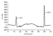
레이저 에너지가 흡수되는 깊이, 즉 단일 레이저 펄스에 의해 제거되는 나노구조화된 필름 재료의 양은 재료의 (즉, 투명 전도성 박막 및/또는 기판의) 물리적 (광학적 및 기계적 둘 모두) 특성 및 레이저 파장에 따라 좌우될 수 있다. 일부 예시적인 실시 형태에서, 나노구조화된 필름은 은 나노와이어를 포함하는데, 이는 도 13에 나타낸 바와 같이, 일반적으로 340 내지 425 나노미터 범위의 파장의 스펙트럼에 걸쳐 흡광을 나타낸다 (따라서, 잠재적으로 매우 다양한 레이저가 고려될 수 있다).The depth at which the laser energy is absorbed, i.e. the amount of nanostructured film material removed by a single laser pulse, depends on the physical (both optical and mechanical) characteristics of the material (i.e., the transparent conductive thin film and / Can be influenced. In some exemplary embodiments, the nanostructured film comprises silver nanowires, which exhibit absorbance over the spectrum of wavelengths generally in the range of 340 to 425 nanometers, as shown in Figure 13 (thus, potentially very Various lasers can be considered).
어떠한 특정 이론에 의해 구애되고자 하는 것은 아니지만, 전도성 영역들을 분리하는 트레이스에서 전도도가 손실되게 하는 메커니즘은 나노와이어의 레이저-유발 절단(laser-induced severing) 및 나노와이어 네트워크의 붕괴를 수반하는 것으로 보인다. 레이저 트레이스 내의 금속의 존재는 비행 시간형 2차 이온 질량 분광법(time-of-flight secondary-ion mass spectrometry)을 사용하여 입증할 수 있다. 은 나노와이어 투명 전도성 코팅의 경우에, 레이저 트레이스의 영역 내에 금속 나노와이어가 더 이상 존재하지 않더라도, 레이저에 의해 조사된 스팟의 에지 주위에 은 금속이 재침착되어, 조사되지 않은 나노와이어 코팅보다는 덜 이산적이지만 여전히 비-전도성인 코팅을 형성하는 것으로 알려질 수 있다. 따라서, 패턴화된 은 나노와이어-기반 투명 전도체 필름에서는, 은이 전도성 영역 내에서는 이산된 나노와이어의 형태로 존재하지만 트레이스 내에서는 덜 이산되고 더욱 균일하나 여전히 비-전도성인 층으로서 존재할 수 있다. 데이터는 또한 크레비스 내의 높아진 은 수준에 대한 어떠한 증거도 나타내지 않는데, 이는 은 나노와이어가 레이저 조사에 의해 본질적으로 완전히 재분배될 수 있음을 시사한다.While not wishing to be bound by any particular theory, it is believed that the mechanism of loss of conductivity in the traces separating the conductive regions appears to involve laser-induced severing of the nanowires and collapse of the nanowire network. The presence of metals in the laser traces can be demonstrated using time-of-flight secondary-ion mass spectrometry. In the case of silver nanowire transparent conductive coatings, silver metal is re-deposited around the edge of the spot irradiated by the laser, even though there are no more metal nanowires in the region of the laser trace, Can be known to form discrete but still non-conductive coatings. Thus, in patterned silver nanowire-based transparent conductor films, silver may be present in the form of discrete nanowires in the conductive region, but as a less discrete, more uniform, still non-conductive layer in the trace. The data also show no evidence for elevated silver levels within the crevices suggesting that the silver nanowires can be essentially completely redistributed by laser irradiation.
실시 형태Embodiment
항목 1.
투명 기판과;A transparent substrate;
투명 기판의 주 표면의 적어도 일부분 상에 배치되며 복수의 상호연결 금속성 나노와이어를 포함하는 전기 전도성 층, 및An electrically conductive layer disposed on at least a portion of the major surface of the transparent substrate and comprising a plurality of interconnecting metallic nanowires,
전기 전도성 층의 적어도 일부분 상에 배치된 중합체 오버코트 층을 포함하는 복합층을 포함하며;A composite overcoat layer comprising a polymeric overcoat layer disposed on at least a portion of the electrically conductive layer;
여기서, 복합층의 패턴은 복합층의 x-y 평면의 x-축 및 y-축과 복합층의 x-y 평면 내로의 z-축을 포함하고, 패턴은 복합층의 x-y 평면에서 복수의 전기 전도성 영역을 형성하고, 전기 전도성 영역들은 전기 절연성 트레이스들에 의해 서로 분리되고, 각각의 전기 절연성 트레이스는 복합층의 x-y 평면의 z-축 내로 밸리를 형성하고, 밸리는 복합층의 x-y 평면에 대해 최대 깊이가 10 나노미터 내지 100 나노미터의 범위이고, 밸리는 단면 폭이 10 마이크로미터 내지 1000 마이크로미터의 범위이고, 밸리는 복합층의 x-y 평면의 z-축 내로 추가로 50 나노미터 내지 100 나노미터 범위의 깊이를 갖는 복수의 크레비스를 추가로 포함하는 투명 전기 전도체.Here, the pattern of the multiple layer includes the x-axis and y-axis of the xy plane of the multiple layer and the z-axis into the xy plane of the multiple layer, and the pattern forms a plurality of electrically conductive regions in the xy plane of the multiple layer , The electrically conductive regions are separated from each other by electrically insulating traces, each electrically insulating trace forming a valley in the z-axis of the xy plane of the composite layer, the valley having a maximum depth in the xy plane of the composite layer of less than 10 nanometers And the valley has a cross-sectional width in the range of 10 micrometers to 1000 micrometers and the valley has a depth in the range of 50 nanometers to 100 nanometers further into the z-axis of the xy plane of the composite layer And further comprising a plurality of crevices having a plurality of crevices.
항목 2. 항목 1에 있어서, 적어도 일부의 크레비스의 깊이는, 복합층의 x-y 평면에 대해, 복합층의 x-y 평면의 z-축 내로 100 나노미터 이상인 투명 전기 전도체.Item 2. The transparent electric conductor according to
항목 3. 항목 1 또는 항목 2에 있어서, 밸리는 밸리의 에지를 따라 측면 릿지(lateral ridge)를 가지며, 측면 릿지는 밸리의 최대 깊이에 대해 표면 평면 위로 z-축을 따라 1% 이하로 융기하는 투명 전기 전도체.
항목 4. 항목 1 내지 항목 3 중 어느 하나에 있어서, 중합체 오버코트 층은 적어도 하나의 다작용성 (메트)아크릴레이트의 반응 생성물을 포함하는 투명 전기 전도체.Item 4. The transparent electric conductor according to any one of
항목 5. 항목 1 내지 항목 4 중 어느 하나에 있어서, 중합체 오버코트 층은 금속 산화물 나노입자를 포함하는 투명 전기 전도체.
항목 6. 항목 1 내지 항목 5 중 어느 하나에 있어서, 중합체 오버코트 층은 전기활성(electroactive) 중합체를 포함하는 투명 전기 전도체.Item 6. The transparent electric conductor according to any one of
항목 7. 항목 1 내지 항목 6 중 어느 하나에 있어서, 복수의 상호연결 금속성 나노와이어는 은을 포함하는 투명 전기 전도체.
항목 8. 항목 1 내지 항목 7 중 어느 하나에 있어서, 투명 기판은 약 5 마이크로미터 내지 약 1000 마이크로미터 범위의 두께를 갖는 층인 투명 전기 전도체.Item 8. The transparent electric conductor according to any one of
항목 9. 항목 1 내지 항목 8 중 어느 하나에 있어서, 전기 전도성 층은 두께가 약 50 나노미터 내지 약 1 마이크로미터의 범위인 투명 전기 전도체.Item 9. The transparent electric conductor according to any one of
항목 10. 항목 1 내지 항목 9 중 어느 하나에 있어서, 복합층은 두께가 약 50 나노미터 내지 약 1 마이크로미터의 범위인 투명 전기 전도체.
항목 11. 항목 1 내지 항목 10 중 어느 하나에 있어서, 전기 절연성 트레이스는 복수의 전기 전도성 영역에서 전기 전도성 영역들 사이에 1 메가옴 초과의 전기 저항을 제공하는 투명 전기 전도체.Item 11. The transparent electrical conductor according to any one of
항목 12. 항목 1 내지 항목 11 중 어느 하나의 투명 전기 전도체를 포함하는 물품.
항목 13. 항목 1 내지 항목 11 중 어느 하나의 투명 전극을 제조하는 방법으로서,Item 13. A method for manufacturing a transparent electrode according to any one of
투명 기판과;A transparent substrate;
투명 기판의 주 표면의 적어도 일부분 상에 배치되며 복수의 상호연결 금속성 나노와이어를 포함하는 전기 전도성 층, 및An electrically conductive layer disposed on at least a portion of the major surface of the transparent substrate and comprising a plurality of interconnecting metallic nanowires,
전기 전도성 층의 적어도 일부분 상에 배치된 중합체 오버코트 층을 포함하는 복합층을 포함하는 투명 전기 전도성 필름을 제공하는 단계; 및Providing a transparent electrically conductive film comprising a composite layer comprising a polymeric overcoat layer disposed on at least a portion of the electrically conductive layer; And
패턴에 따라 투명 전기 전도성 필름을 패턴식 조사하여 투명 전극을 제공하는 단계를 포함하는 방법.Patterning the transparent electrically conductive film according to the pattern to provide a transparent electrode.
항목 14. 항목 13에 있어서, 패턴 조사는 레이저를 사용한 조사를 포함하는 방법.
항목 15. 항목 14에 있어서, 레이저는 펄스형 UV 레이저인 방법.
항목 16. 항목 14에 있어서, 레이저는 연속파 UV 레이저인 방법.
항목 17. 항목 13 내지 항목 16 중 어느 하나에 있어서, 패턴식 조사는 투명 전기 전도성 필름의 롤-투-롤 처리를 포함하는 방법.Item 17. The method according to any one of items 13 to 16, wherein the patterned irradiation comprises roll-to-roll processing of the transparent electroconductive film.
항목 18. 항목 13에 있어서, 패턴식 조사는 복수의 상호연결 금속성 나노와이어 중 적어도 일부를 절단하는 것을 포함하는 방법.
항목 19. 항목 13에 있어서, 패턴식 조사는 조사된 영역 내에서의 복수의 상호연결 금속성 나노와이어 중 적어도 일부의 붕괴 및 조사된 영역 내에서의 금속성 나노와이어로부터 비-전도성, 비-나노와이어 층 내로의 금속의 재분배를 포함하는 방법.Item 19. The method of item 13, wherein the patterned irradiation is performed by decaying at least a portion of a plurality of interconnected metallic nanowires within the irradiated region and from the metallic nanowires within the irradiated region to a non-conductive, non- ≪ / RTI >
[실시예][Example]
탭핑 모드(Tapping Mode)의, 원자력 현미경 ("AFM")Tapping Mode, Atomic Force Microscopy (AFM)
원자력 현미경 ("AFM") 장비 (미국 캘리포니아주 산타 바바라 소재의 비코 인스트루먼츠, 인크.(Veeco Instruments, Inc.)로부터 상표명 "비코 디멘션(VEECO DIMENSION) 5000"으로 입수함, "나노스코프(NANOSCOPE) III" 제어기를 포함함)를 사용하여 본 발명의 투명 전극을 분석하였다. 사용된 탐침은, 42 뉴턴/미터의 공칭 힘 상수 및 300 킬로헤르츠의 공칭 공명 주파수를 갖는, 올림푸스(Olympus) 에칭된 규소 탐침 ("OTESPA" 탐침, 1 Ωcm 규소 재료)이었다. 분석 소프트웨어 (미국 캘리포니아주 산타 바바라 소재의 브루커 나노, 인크.(Bruker Nano, Inc.)로부터의 상표명 "나노스코프 어낼러시스"(NANOSCOPE ANALYSIS))를 사용하여 데이터를 분석하였다. 이미지를 평탄화 (스캔 라인들 사이의 z-오프셋을 제거하도록 0차) 및/또는 평면-피팅 (1차)하여 샘플 틸트(sample tilt)를 제거하였다. AFM 이미지 (예를 들어, 도 5a, 도 6a, 도 7a, 도 8a, 도 10a 및 도 12a)에서, 더 밝은 영역은 샘플의 평균 x-y 평면 위의 z-축 값을 나타내는 반면, 더 어두운 영역은 샘플의 평균 x-y 평면 아래의 z-축 값을 나타낸다. AFM 프로파일에서, (예를 들어, 도 5b, 도 5c, 도 6b, 도 7b, 도 8b, 도 10b 및 도 12b에서), z-축의 원점은 프로파일 분석 데이터세트 내의 (조사되지 않은 랜드(land) 영역) 높이 이미지(즉, 토포그래피(topography) 이미지)의 모든 z-값들의 평균 높이와 일치하도록 지정하였다. 도 5a, 도 6a, 도 7a, 도 8a, 도 10a, 도 12a 및 도 14a의 AFM 이미지에서, 이미지화된 영역은 샘플의 x-y 평면 내의 70 마이크로미터 x 70 마이크로미터이다.Nucleoscopic microscope ("AFM") equipment (available from Veeco Instruments, Inc., Santa Barbara, CA, under the trade designation "VEECO DIMENSION 5000", "NANOSCOPE III "Controller) was used to analyze the transparent electrode of the present invention. The probe used was an Olympus etched silicon probe ("OTESPA" probe, 1 Ωcm silicon material) with a nominal force constant of 42 Newton / meter and a nominal resonant frequency of 300 kilohertz. Analysis software (NANOSCOPE ANALYSIS, from Bruker Nano, Inc., Santa Barbara, CA) was used to analyze the data. The sample tilt was removed by flattening the image (zero order to eliminate the z-offset between the scan lines) and / or plane-fitting (primary). In the AFM images (e.g., Figures 5A, 6A, 7A, 8A, 10A and 12A), the lighter regions represent the z-axis values on the average xy plane of the sample, Represents the z-axis value below the mean xy plane of the sample. In the AFM profile, the origin of the z-axis is defined as the (untreated land) position in the profile analysis data set (e.g., in Figures 5b, 5c, 6b, 7b, 8b, 10b and 12b) Area) height image (i. E., Topography image). In the AFM images of Figures 5A, 6A, 7A, 8A, 10A, 12A and 14A, the imaged region is 70 micrometers x 70 micrometers in the x-y plane of the sample.
재료material
하기의 실시예에서 사용된 재료가 표 1에 설명되어 있다. 모든 재료들은 입수된 원상태로(as received) 사용하였다.The materials used in the following examples are described in Table 1. All materials were used as received.
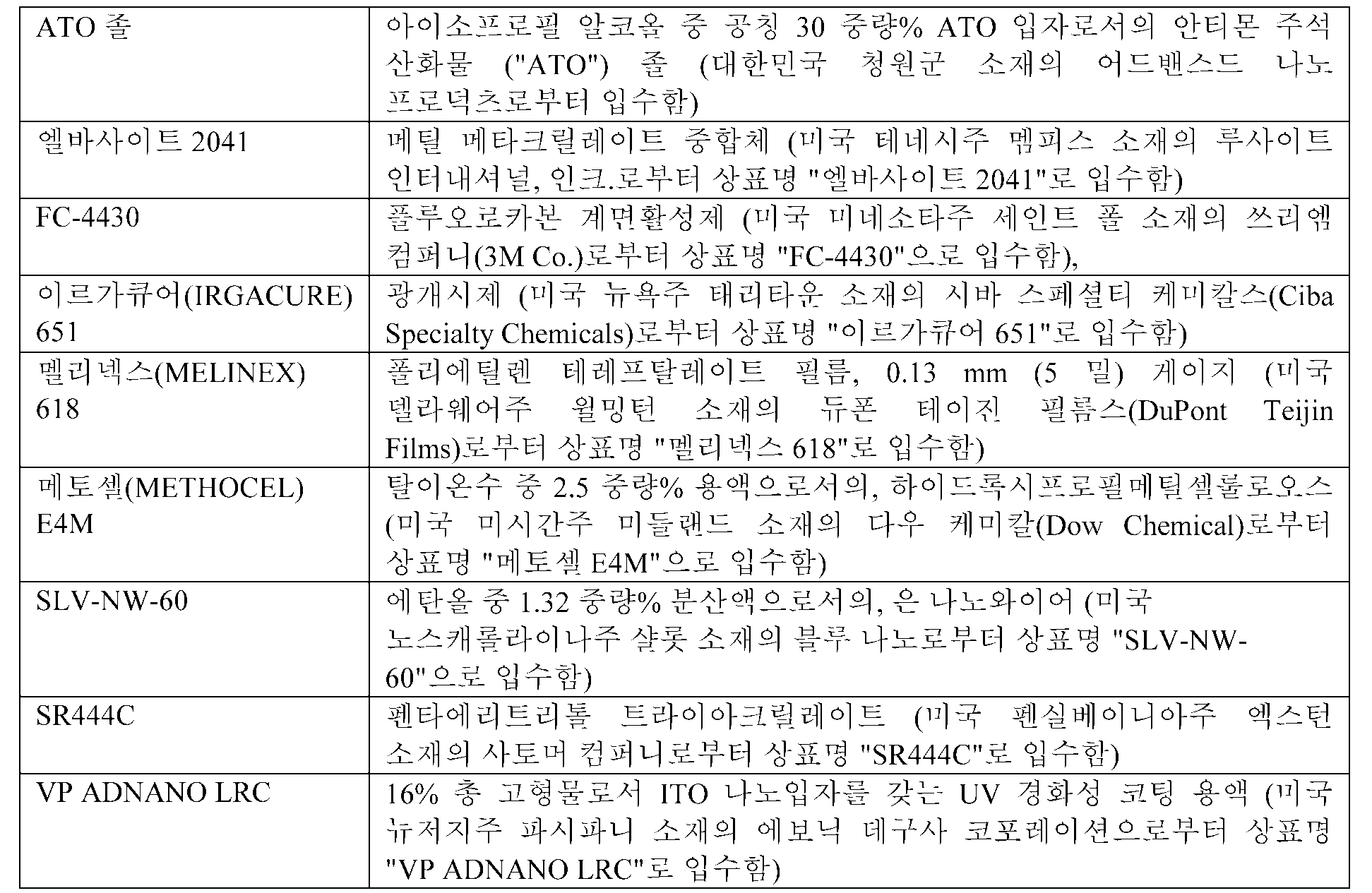
오버코트 조성물 OC-1 내지 OC-3의 제조Preparation of overcoat compositions OC-1 through OC-3
본 명세서에 전체적으로 참고로 포함된, 계류 중인 미국 가특허 출원 제61/475860호 (펠러라이트(Pellerite) 등, 2011년 4월 15일자로 출원됨)에 기재된 바와 같이, 오버코트 조성물을 제조하였다.An overcoat composition was prepared as described in pending U.S. Provisional Patent Application No. 61/475860 (Pellerite et al., Filed April 15, 2011), which is incorporated herein by reference in its entirety.
오버코트 조성물 "OC-1"의 제조Production of overcoat composition "OC-1"
SR444C 및 엘바사이트 2041의 85:15 중량-대-중량 ("w/w") 혼합물을 아세톤 중에 10 중량% 총 고형물로 용해시켜 농축물(concentrate)을 제조하였다. 이르가큐어 651을 0.2 중량%의 총 고형물로 첨가하였다. 중량 기준으로 1:1의 아이소프로필 알코올:다이아세톤 알코올 중에 희석하여 3 중량% 고형물의 코팅 용액을 얻었다.A concentrate was prepared by dissolving a 85:15 weight-to-weight ("w / w") mixture of SR444C and Elbasite 2041 in a 10 wt% total solids in acetone. Irgacure 651 was added as a total solids content of 0.2% by weight. Diluted in a 1: 1 isopropyl alcohol: diacetone alcohol on a weight basis to obtain a coating solution of 3 wt% solids.
오버코트 조성물 "OC-2"의 제조Production of overcoat composition "OC-2"
사용 직전에 VP ADNANO LRC를 1:1 아이소프로필 알코올:다이아세톤 알코올 중에 5 중량%의 총 고형물로 희석하였다.VP ADNANO LRC was diluted with a total solids content of 5% by weight in 1: 1 isopropyl alcohol: diacetone alcohol.
오버코트 조성물 "OC-3"의 제조Production of overcoat composition "OC-3"
SR444C 및 엘바사이트 2041의 85:15 (w/w) 혼합물을 아세톤 중에 10 중량%의 총 고형물로 용해시켜 농축물을 제조하였다. 이르가큐어 651을 0.2 중량%의 총 고형물로 첨가하였다. 적절한 양의 이러한 농축물 및 ATO 졸을 혼합하고 1:1 (w/w) 아이소프로필 알코올:다이아세톤 알코올 중에 희석하여 3 중량% ATO 및 2 중량% 아크릴 고형물을 함유하는 오버코트 용액을 얻었다.A concentrate was prepared by dissolving a 85:15 (w / w) mixture of SR444C and Elvacite 2041 in acetone to a total solids content of 10% by weight. Irgacure 651 was added as a total solids content of 0.2% by weight. Appropriate amounts of this concentrate and ATO sol were mixed and diluted in 1: 1 (w / w) isopropyl alcohol: diacetone alcohol to yield an overcoat solution containing 3 wt% ATO and 2 wt% acrylic solids.
은 나노와이어 잉크의 제조Manufacture of silver nanowire inks
입구가 넓은 스크류 마개 병(wide mouth screw top jar)을 58.85 그램의 0.05 중량% FC-4430 용액 및 12.57 g의 2.5 중량% 메토셀 E4M 용액으로 충전하고, 20:20 시력을 갖는 육안으로 보아 균질해질 때까지 혼합물을 휘저었다. 이어서, 휘저으면서, SLV-NW-60 은 나노와이어 분산액을, 총 26.78 그램의 분산액이 첨가될 때까지, 나누어서 첨가하였다. 은 나노와이어의 균일한 분산을 보장하도록 혼합물을 손으로 휘저었고, 이어서 추가적인 49.1 그램의 0.05 중량% FC-4430 용액을 첨가하고 균질해질 때까지 혼합물을 손으로 교반하였다. 최종 분산액은 0.24 중량% 은 나노와이어, 0.21 중량% 하이드록시프로필-메틸셀룰로오스, 및 0.037 중량% FC-4430이었다.A wide mouth screw top jar was filled with 58.85 grams of a 0.05 wt% FC-4430 solution and 12.57 grams of a 2.5 wt% Methocel E4M solution and homogenized visually with a 20:20 visual acuity Until the mixture was stirred. Subsequently, while stirring, the SLV-NW-60 nanowire dispersion was added in portions until a total of 26.78 grams of dispersion was added. Was hand rolled to ensure uniform dispersion of the nanowires and then an additional 49.1 grams of a 0.05 wt% FC-4430 solution was added and the mixture was hand stirred until homogeneous. The final dispersion was 0.24 wt% silver nanowire, 0.21 wt% hydroxypropyl-methylcellulose, and 0.037 wt% FC-4430.
투명 전극 TE1 내지 TE4의 제조Production of transparent electrodes TE1 to TE4
상기에서 제조된 은 나노와이어 잉크를, 3 m/min (10 ft/min)의 웨브 속도, 4.0 cc/min의 잉크 유량, 19.7 m/sec의 건조 오븐 공기유동, 및 75℃ (구역 1) 및 120℃ (구역 2)의 건조 오븐 온도에서 작동하는 10.2 cm (4 인치) 슬롯 다이 코팅기를 사용하여, 15.2 cm (6 인치) 폭, 0.13 mm (5 밀) 게이지 멜리넥스 618 필름 상에 코팅하였다. 오버코트 조성물 "OC-1" (3 중량% 고형물) 및 "OC-2" (5 중량% 고형물)를 사용하여 상기 필름에 오버코팅하여 투명 전극 필름을 제조하였다. 상기 오븐 및 공기 유동 설정, 6.1 m/min (20 ft/min)의 웨브 속도, (표 2에 표시된 바와 같은) 5 또는 7 cc/min의 용액 유량, 21℃ (70℉)의 UV 플레이트 온도, 질소 분위기, 및 100% UV 램프 출력을 사용하여, 잉크 코팅용으로 사용되는 10.2 cm (4 인치) 다이 코팅기에서 코팅을 수행하였다. 이러한 절차는 200 nm 내지 400 nm 범위의 공칭 두께의 오버코트를 제공하였다. 탁도계 (미국 메릴랜드주 콜럼비아 소재의 비와이케이-가드너 유에스에이(BYK-Gardiner USA)로부터 상표명 "헤이즈-가드 플러스"로 입수함)를 사용하여 투과율 및 탁도를 측정하였고, 무접점 저항 탐침 (미국 위스콘신주 프레스컷 소재의 델콤 인스트루먼츠, 인크.(Delcom Instruments Inc.)로부터 상표명 "모델(MODEL) 717B"로 입수함)을 사용하여 시트 저항을 측정하였다. 그 결과가 표 2에 나타나 있다.The silver nanowire inks prepared above were coated at a web speed of 3 m / min (10 ft / min), an ink flow rate of 4.0 cc / min, a dry oven air flow of 19.7 m / (6 inches) wide by 0.13 mm (5 mil) gauge Mellinex 618 film using a 10.2 cm (4 inch) slot die coater operating at a drying oven temperature of 120 deg. C (Zone 2). A transparent electrode film was prepared by overcoating the film with an overcoat composition "OC-1" (3 wt% solids) and "OC-2" (5 wt% solids). The oven and air flow settings, web speeds of 20 ft / min, solution flow rates of 5 or 7 cc / min (as shown in Table 2), UV plate temperature of 21 DEG C (70 DEG F) The coating was performed in a 10.2 cm (4 inch) die coater used for ink coating, using a nitrogen atmosphere, and a 100% UV lamp output. This procedure provided an overcoat of nominal thickness ranging from 200 nm to 400 nm. Transmittance and turbidity were measured using a turbidimeter (available under the trade designation "Hayes-Guard Plus " from BYK-Gardiner USA, Columbia, Maryland) and a contactless resistance probe The sheet resistance was measured using a cut material available from Delcom Instruments Inc. under the trade designation "MODEL 717B ". The results are shown in Table 2.
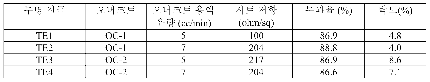
실시예 1 - 투명 전극 TE1 내지 TE4의 레이저 패턴식 조사Example 1 - Laser patterning of transparent electrodes TE1 to TE4
상기 투명 전극을, 20 ns 펄스 폭으로 355 nm에서 작동하는 Nd:YVO4 레이저가 구비된 레이저 시스템 (미국 오리건주 포틀랜드 소재의 이에스아이(ESI)로부터 상표명 "5100 레이저 시스템(LASER SYSTEM)"으로 입수함)을 사용하여 패턴화하였다. 기타 파라미터는 다음과 같았다: 바이트 크기(bite size)는 15 마이크로미터였고, 속력은 300 mm/sec였고, 반복률(repetition rate)은 20 ㎑였고, 레이저 출력은 하기 표 3, 표 4 및 표 5에 열거된 바와 같이 60, 100, 150, 또는 215 밀리와트 ("mW") 중 어느 하나였다.The transparent electrode was obtained as a laser system (trade name "5100 Laser System" from ESI, Portland, OR) equipped with an Nd: YVO4 laser operating at 355 nm with a 20 ns pulse width ). The other parameters were as follows: Bite size was 15 micrometers, speed was 300 mm / sec, repetition rate was 20 kHz, and laser power was measured in the following Tables 3, 4 and 5 Was either 60, 100, 150, or 215 milliwatts ("mW") as listed.
상기한 조건을 사용하여, 각각의 투명 전극 상에 레이저로 2.54 cm (1 인치) 정사각형 패턴을 그렸다 (즉, 에칭하였다). 2점 탐침을 사용해 정사각형의 내측과 외측 사이의 전기 저항을 측정함으로써 전기 절연성(electrical isolation)을 평가하였으며, 메가옴 단위로 측정하였다. 전기 절연성을 결정하기 위한 저항 측정 결과가 표 3에 나타나있다.Using the above conditions, a 2.54 cm (1 inch) square pattern was drawn (i.e., etched) with a laser on each transparent electrode. The electrical insulation was evaluated by measuring the electrical resistance between the inside and the outside of the square using a two-point probe, measured in megahertz. The results of the resistance measurement for determining electrical insulation are shown in Table 3.

표 3에서, "있음"으로 표시된 것은 레이저-에칭된 2.54 cm (1 인치) 정사각형의 내측과 외측 사이의 레이저 트레이스를 가로질러 측정된 저항이 1 메가옴 초과였음을 의미하는 한편, "없음"으로 표시된 것은 레이저-에칭된 정사각형의 내측과 외측 사이의 레이저 트레이스를 가로질러 측정된 저항이 1 메가옴 이하였음을 의미하였다.In Table 3, denoted as "Present" means that the measured resistance across the laser trace between the inner and outer sides of the laser-etched square of 2.54 cm (1 inch) was greater than 1 mega The indication indicated that the measured resistance across the laser traces between the inside and outside of the laser-etched square was less than 1 megohm.
가시광 현미경 및 원자력 현미경에 의한 추가의 분석을 위해 투명 전극 TE1 및 TE4를 선택하였다. 모두 4가지 레이저 출력 수준에서 제조된 트레이스의 암시야 가시광 현미경 사진이 (TE1에 대해) 도 3a 내지 도 3d에, 그리고 (TE4에 대해) 도 4a 내지 도 4d에 나타나있다 (투명 전극 및 레이저 조사 출력 수준과 도면 번호의 관계에 대해서는 표 4 참조).Transparent electrodes TE1 and TE4 were selected for further analysis by visible light microscopy and atomic force microscopy. A dark field visible light micrograph (for TE1) of the traces produced at all four laser power levels is shown in Figures 3a to 3d and (for TE4) Figures 4a to 4d See Table 4 for the relationship between level and drawing number).
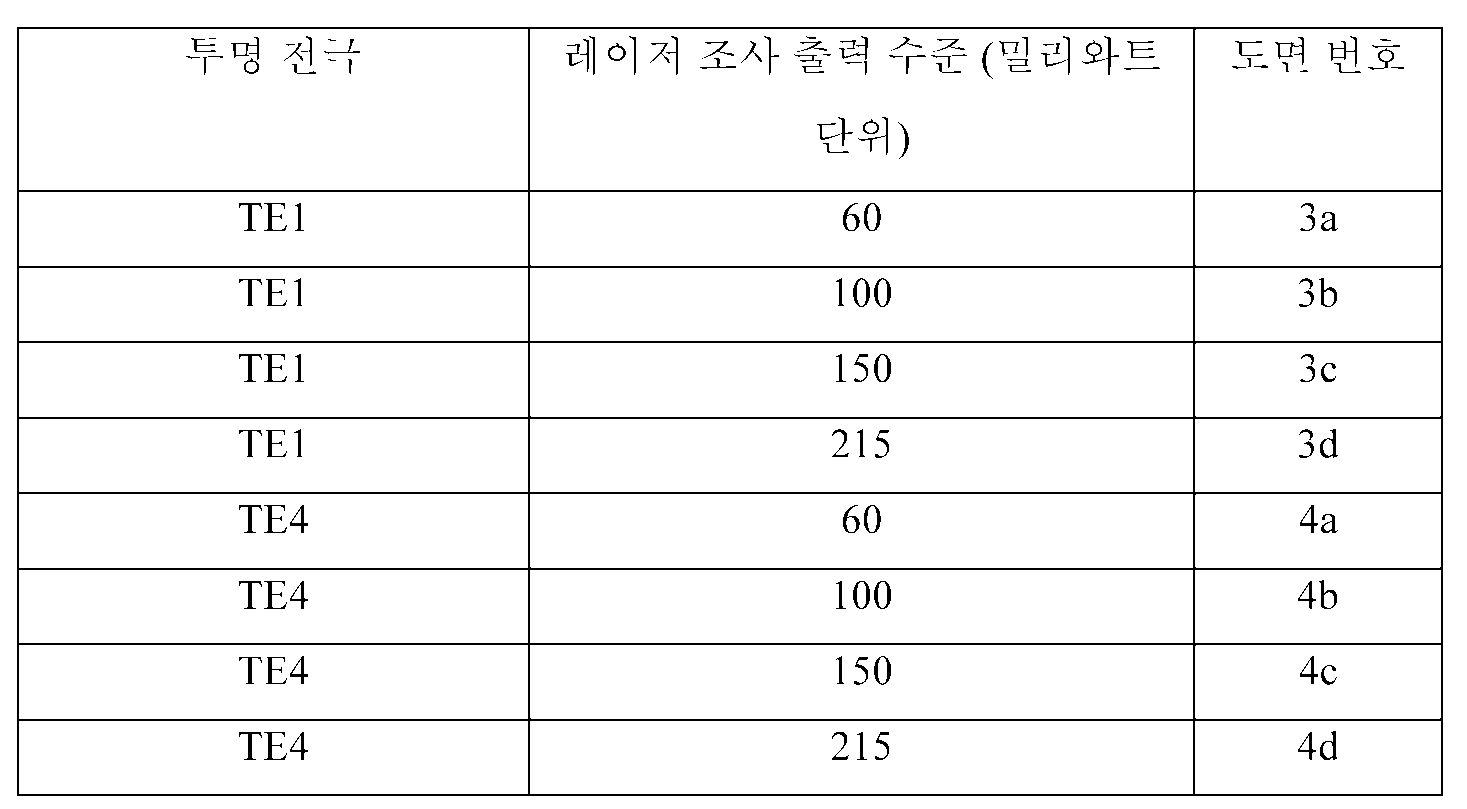
도 3a 내지 도 3d 및 도 4a 내지 도 4d는 트레이스 구조에 대한 레이저 출력 변화의 영향을 나타내었다. 충분히 높은 출력 수준에서, 전기 절연성 트레이스를 제조하는 데 필요한 것을 초과하는 출력에서는 기판에 대한 손상이 분명해졌다. 그러한 손상은 레이저 조사 중간에 밝은 스팟(37, 47)으로서 나타났다. 밝은 스팟(37, 47)(및 37', 47')은 레이저 출력이 증가함에 따라 더 커졌다. 이러한 밝은 스팟은 조사되지 않은 랜드 영역(33, 34)(및 43, 44)의 x-y 평면 위로 융기된 프로파일 특징부에 상응할 수 있다.Figures 3a-3d and 4a-4d show the effect of laser power variation on the trace structure. At sufficiently high power levels, damage to the substrate has become evident at an output exceeding what is required to produce an electrically insulative trace. Such damage appeared as
"탭핑 모드의 AFM" 방법에 따라, 선택된 레이저 트레이스의 AFM 이미지 및 AFM 프로파일을 생성하였다. 상응하는 투명 전극 샘플, 조사 출력, 및 도면 번호가 표 5에 표시되어 있다.In accordance with the "AFM of tapping mode" method, AFM images and AFM profiles of the selected laser traces were generated. The corresponding transparent electrode samples, irradiation power, and reference numerals are shown in Table 5.

도 5a는 투명 전극의 예시적인 실시 형태에서의 레이저 트레이스의 원자력 현미경 이미지 (높이 또는 토포그래피)이다. 이미지화된 영역은 x-y 평면 내의 70 마이크로미터 x 70 마이크로미터이며, 가장 어두운 톤으로부터 가장 밝은 톤까지의 범위는 z-방향으로 140 nm의 높이를 나타낸다. 도 5b 및 도 5c는 도 5a의 레이저 트레이스의 프로파일 분석 결과이다. 도 5a에서, 라인(510)은 도 5b의 AFM 프로파일을 생성하기 위해 분석된 이미지의 부분을 나타낸다. 도 5a에서의 어두운 라인(501, 502, 503, 504)은 각각 도 5b에서의 크레비스(501', 502', 503', 504')와 부합한다. 도 5b에서 레이저 트레이스의 "밸리"는 약 20 nm 깊이 및 약 12 마이크로미터 폭인 것으로 관찰되었는데, 크레비스가 z-축을 따라 약 80 나노미터까지 (즉, 밸리의 최대 깊이보다 z-축을 따라 약 60 nm 더) 연장한다.5A is an atomic force microscope image (height or topography) of a laser trace in an exemplary embodiment of a transparent electrode. The imaged region is 70 micrometers x 70 micrometers in the x-y plane and the range from the darkest tone to the lightest tone represents a height of 140 nm in the z-direction. Figures 5B and 5C show the profile analysis results of the laser traces of Figure 5A. In FIG. 5A,
또한 도 5a를 참조하면, 영역(520)은 도 5c의 AFM 프로파일을 생성하기 위해 분석된 이미지의 부분을 나타낸다. 이러한 분석 결과에서는, 최대 밸리 깊이의 관점이 강조되는 반면, 레이저의 경로를 따르는 z-값들의 평균화로 인해 레이저 트레이스의 경로를 따르는 상대적으로 미세한 크레비스는 덜 분명하였다. 도 5c에서, 최대 밸리 깊이(540)는 또한 x-y 평면(530)으로부터 z-축을 따라 약 20 nm인 것으로 나타났으며, 밸리 폭은 대략 12 마이크로미터 폭이었다. 유사한 영향이 도 6a 및 도 6b에서 나타나는데, 여기서 밸리가 약 100 nm의 최대 깊이(640)를 나타내고, 크레비스(601' 내지 603')가 밸리의 최대 깊이(640)를 최대 100 nm 초과하는 깊이를 갖는다 (크레비스(601 내지 603')는 어두운 라인(601 내지 603)이 도 6a의 라인(610)을 가로지르는 지점에서의 어두운 라인과 부합함).Referring also to Figure 5A,
도 7a 및 도 8a는, 레이저-손상된 스팟(770, 880)에서 관찰되는 바와 같이, 증가된 출력 수준에서의 레이저 조사로 인한 투명 전극 TE1 및 TE4의 손상을 각각 예시한다. 그러나, 레이저-손상된 스팟으로부터 멀리 떨어져서, 어두운 라인(701, 702, 703, 704)이 관찰되었으며, 이는 이들 어두운 라인이 라인(710)을 가로지르는 지점에서 크레비스(701', 702', 703', 704')와 부합하고; 어두운 라인(801, 802, 803)은 이들 어두운 라인이 라인(810)을 가로지르는 지점에서 크레비스(801', 802', 803')와 부합한다. 폭이 약 12 마이크로미터이고 최대 깊이가 약 80 nm인 밸리가 또한 도 8b에 나타나있다.Figures 7a and 8a illustrate damage to transparent electrodes TE1 and TE4, respectively, due to laser irradiation at an increased power level, as observed in laser-damaged
투명 전극 TE5 및 TE6의 제조Production of transparent electrodes TE5 and TE6
국제특허 공개 WO 2008/46058호 (알레만드 등)에 개시된 방법에 따라 제조된, 은 나노와이어 분산액 및 UV-경화성 아크릴 보호 오버코트의 3.1 중량% 고형물 용액을 사용하여, 멜리넥스 618 필름의 프라이밍된 면 상에 은 나노와이어 투명 전도체 코팅 (TCC)을 제조하였다. 4.6 m/min (15 ft/min)의 웨브 속도, 23 cc/min의 잉크 유량, 및 40℃ (구역 1), 80℃ (구역 2), 및 120℃ (구역 3)의 건조 오븐 온도에서 작동하는 25.4 cm (10 인치) 다이 코팅기를 사용하여 은 분산액을 적용하였다. 상기 오븐 및 공기 유동 설정, 9.1 m/min (30 ft/min)의 웨브 속도, 20 cc/min의 용액 유량, 21℃ (70℉)의 UV 백업 롤 온도, 질소 분위기, 및 100% UV 램프 (H 전구) 출력을 사용하여, 은 잉크 코팅용으로 사용되는 25.4 cm (10 인치) 다이 코팅기에서 오버코트를 적용하였다. TE5로 지정된 이 필름은, 투명 전극 TE1 내지 TE4의 제조에 있어서 설명된 방법을 사용하여 측정되는, 103 ohm/sq의 시트 저항, 89.5%의 가시광 투과율, 2.6%의 탁도를 나타내었다.Using a silver nanowire dispersion and a 3.1 wt% solids solution of a UV-curable acrylic protective overcoat prepared according to the method disclosed in International Patent Publication No. WO 2008/46058 (Alleman et al.), Primed surfaces of Melinex 618 film A silver nanowire transparent conductor coating (TCC) was prepared. A web speed of 4.6 m / min (15 ft / min), an ink flow rate of 23 cc / min, and a drying oven temperature of 40 ° C (zone 1), 80 ° C (zone 2), and 120 ° C (zone 3) A silver dispersion was applied using a 25.4 cm (10 inch) die coater. The oven and air flow settings, a web speed of 9.1 m / min (30 ft / min), a solution flow rate of 20 cc / min, a UV back-up roll temperature of 21 DEG C (70 DEG F), a nitrogen atmosphere, H bulb) output, an overcoat was applied on a 25.4 cm (10 inch) die coater used for silver ink coating. This film designated as TE5 exhibited a sheet resistance of 103 ohm / sq, a visible light transmittance of 89.5%, and a haze of 2.6%, which were measured using the method described in the production of transparent electrodes TE1 to TE4.
은 잉크 유량이 25 cc/min이고, 상기 오버코트를 상기한 바와 같이 제조된 용액 OC-3으로 대체하고, 오버코트 용액 유량이 18 cc/min인 점을 제외하고는 동일한 재료 및 절차를 사용하여, 두 번째 로트의 필름을 제조하였다. TE6으로 지정된 이 필름은, 예시적인 투명 전극 TE1 내지 TE4의 제조에 있어서 설명된 방법을 사용하면, 60 ohm/sq의 시트 저항, 86%의 투과율, 및 2.3%의 탁도를 나타내었다., The ink flow rate was 25 cc / min, the overcoat was replaced with the solution OC-3 prepared as described above, and the same overcoat solution was used, with the same materials and procedures except that the overcoat solution flow rate was 18 cc / Lt; / RTI > This film, designated TE6, exhibited a sheet resistance of 60 ohm / sq, a transmittance of 86%, and a turbidity of 2.3% using the method described in the preparation of the exemplary transparent electrodes TE1 to TE4.
실시예 2 - 투명 전극 TE5 및 TE6의 레이저 패턴식 조사Example 2 - Laser patterning of transparent electrodes TE5 and TE6
GSI 3-D 아날로그 스캐너 (모델 번호 E10-202861)가 구비된, 355 nm에서 작동하는 삼중 주파수 Nd:YVO4 레이저 (미국 캘리포니아주 산타클라라 소재의 코히어런트 아비아(Coherent Avia)로부터 입수함)를 사용하여, 레이저 조사를 수행하였다. 레이저 파라미터는 다음과 같았다: 펄스 반복률: 40 ㎑, 펄스 지속 시간: 대략 50 nsec, 레이저 피크 출력: 0.44 W, 단일 펄스 에너지: 22 μJ, 펄스 피크 출력: 440 W, 포커싱된 스팟 크기(focused spot size): 직경이 대략 68 μ, 스캔 속도: 500 mm/sec. 이러한 실험을 위해 피크 출력을 55 내지 70%로 감쇠시켰다. 이러한 레이저 조건을 사용하여, 상기에 기재된 투명 전도성 필름에, 한 변이 약 2.5 cm (1 인치)인 정사각형 패턴의 형상으로 트레이스를 에칭하였다. 2점 탐침 및 전압계를 사용하여 정사각형의 내부와 외부의 전기 절연성을 평가하였고, 가시광 현미경 및 원자력 현미경에 의해 트레이스를 분석하였다.A triple-frequency Nd: YVO4 laser (available from Coherent Avia, Santa Clara, Calif.) Operating at 355 nm, equipped with a GSI 3-D analog scanner (model number E10-202861) , Laser irradiation was performed. The laser parameters were as follows: Pulse Repetition Rate: 40 kHz, Pulse Duration: Approximately 50 nsec, Laser Peak Output: 0.44 W, Single Pulse Energy: 22 μJ, Pulse Peak Output: 440 W, focused spot size ): Diameter of approximately 68 mu, scan speed: 500 mm / sec. The peak output was attenuated to 55-70% for this experiment. Using these laser conditions, the traces were etched into the transparent conductive film described above in the shape of a square pattern of about 2.5 cm (1 inch) on each side. Two - point probes and voltmeters were used to evaluate the electrical insulation of the inside and the outside of the square, and traces were analyzed by visible light microscopy and atomic force microscopy.
투명 전극 TE5 및 TE6의 필름 샘플을 상기 UV 레이저 처리 조건에 처하게 하여, 55 내지 70% 레이저 출력에서 레이저-에칭된 정사각형 패턴을 얻었다. 정사각형의 내측 지점과 외측 지점 사이의 전기 저항의 2점 탐침 측정을 사용하여 전기 절연성의 정도를 평가하였고, 결과가 표 6에 나타나있다.Film samples of transparent electrodes TE5 and TE6 were subjected to the UV laser treatment conditions to obtain a laser-etched square pattern at a 55 to 70% laser output. The degree of electrical insulation was evaluated using a two-point probe measurement of the electrical resistance between the inner and outer points of the square, and the results are shown in Table 6.

개방-회로 저항 (>1 메가옴)의 관찰을 전기 절연성에 대한 증거로서 취하였다.Observations of open-circuit resistance (> 1 megohm) were taken as evidence for electrical insulation.
도 9a 및 도 9b는 각각 TE5 및 TE6의 조사되지 않은 (즉, 대조군) 영역의 AFM 이미지를 나타낸다. 이미지화된 영역은 각각의 그러한 이미지 내의 10 마이크로미터 x 10 마이크로미터였다.Figures 9A and 9B show AFM images of the unexposed (i.e., control) area of TE5 and TE6, respectively. The imaged area was 10 micrometers by 10 micrometers in each such image.
도 10a는 투명 전극의 예시적인 실시 형태에서의 레이저 트레이스의 원자력 현미경 이미지 (높이 또는 토포그래피)이다. 이미지화된 영역은 x-y 평면에서 70 마이크로미터 x 70 마이크로미터이며, 가장 어두운 톤으로부터 가장 밝은 톤까지의 범위는 z-방향으로 300 nm의 높이를 나타낸다. 도 10b는 도 10a의 레이저 트레이스의 프로파일 분석 결과이다. 도 10a 및 도 10b는 63% 레이저 출력에서의 TE5의 레이저 트레이스의 AFM 이미지 및 프로파일 분석 결과이다. 도 10a에서 라인(1010)은 도 10b의 AFM 프로파일을 생성하기 위해 분석된 이미지의 부분을 나타낸다. 도 10a에서의 밝은 스팟은 젤 미립자로 인한 것으로 여겨지며, 레이저 처리와는 관련이 없다. 도 11은, 조사되지 않은 영역의 전도성 메시의 이산된 구조 및 나노와이어의 기하학적 형태를 나타내는, 도 10a에서의 트레이스의 가시광 현미경 사진이다.10A is an atomic force microscope image (height or topography) of a laser trace in an exemplary embodiment of a transparent electrode. The imaged area is 70 micrometers by 70 micrometers in the x-y plane and the range from the darkest tone to the lightest tone represents a height of 300 nm in the z-direction. FIG. 10B is a profile analysis result of the laser trace of FIG. 10A. Figures 10a and 10b show AFM image and profile analysis of the laser traces of TE5 at 63% laser power. 10A,
도 12a는 65% 레이저 출력에서 TE6의 레이저 트레이스의 원자력 현미경 이미지 (높이 또는 토포그래피)이다. 이미지화된 영역은 x-y 평면에서 70 마이크로미터 x 70 마이크로미터이며, 가장 어두운 톤으로부터 가장 밝은 톤까지의 범위는 z-방향으로 300 nm의 높이를 나타낸다. 도 12b는 도 12a의 레이저 트레이스의 프로파일 분석 결과이다. 도 12a에서 라인(1210)은 도 12b의 AFM 프로파일을 생성하기 위해 분석된 이미지의 부분을 나타낸다.12A is an atomic force microscope image (height or topography) of the laser traces of TE6 at 65% laser power. The imaged area is 70 micrometers by 70 micrometers in the x-y plane and the range from the darkest tone to the lightest tone represents a height of 300 nm in the z-direction. 12B is a profile analysis result of the laser trace of FIG. 12A. In FIG. 12A,
투명 전극 TE5에 대한 흡광 스펙트럼의 결정Determination of the absorption spectrum for the transparent electrode TE5
람다(Lambda) 900 UV/가시광 분광광도계 (미국 매사추세츠주 월섬 소재의 퍼킨-엘머(Perkin-Elmer)로부터 입수가능함) 및 하기 절차를 사용하여, 샘플 TE5 상의 은 나노와이어 투명 전도성 코팅에 대해 흡광 스펙트럼을 결정하였다.Using a
1) 코팅되지 않은 PET 필름에 대해 투과율 (%T) 및 반사율 (%R)을 측정한다.1) Measure transmittance (% T) and reflectance (% R) for uncoated PET film.
2) 샘플 TE5에 대해 %T 및 %R을 측정한다.2) Measure% T and% R for sample TE5.
3) 코팅되지 않은 PET ("APET") 및 샘플 TE5 ("ATE5") 둘 모두에 대해 A = 100 - %T - %R을 계산한다.3) Calculate A = 100 -% T -% R for both uncoated PET ("A PET ") and sample TE5 ("A TE5 ").
4) ΔA = APET - ATE5를 계산하고 플롯한다.4) Calculate ΔA = A PET -A TE5 and plot.
얻어지는 ΔA의 플롯이 도 13에 나타나있다. 데이터는 370 nm 근처에서 강한 흡광을 나타내었으며, 이는 400 nm를 지나서 연장되었다. 이는 최대 450 nm의 파장을 갖는 출력을 생성하는 레이저가 이러한 투명 전도성 필름을 패턴화하는 데 사용될 수 있음을 시사한다.A plot of the obtained? A is shown in Fig. The data showed strong absorbance near 370 nm, which extended beyond 400 nm. This suggests that a laser producing an output with a wavelength of up to 450 nm can be used to pattern this transparent conductive film.
비교예 1Comparative Example 1
0.13 mm (5 밀) PET 필름 상의 ITO (미국 코네티컷주 윈저 소재의 테크니-메트(Techni-Met)로부터 입수함; 델콤 시트 저항 125 ohm/sq)의 샘플을 TE5 및 TE6에 사용된 것과 동일한 UV 레이저 처리 조건에 처하게 하여, 55, 60, 65, 및 70% 레이저 출력에서 정사각형 패턴으로 처리된 일련의 샘플을 생성하였다. 추가 샘플은 기판 손상을 최소화하도록 1 m/sec 스캔 속도 및 50% 레이저 출력에서 처리하였다. 후자를 제외한 모든 샘플이 정사각형의 내부와 외부 사이의 전기 절연성을 나타내었다. 샘플을 AFM에 의해 이미지화하고 레이저 트레이스 프로파일 분석하였다.A sample of ITO (available from Techni-Met, Windsor, Conn., USA; Delcom sheet resistance 125 ohm / sq) on a 0.13 mm (5 mil) PET film was exposed to the same UV laser used for TE5 and TE6 Under the processing conditions, a series of samples processed in a square pattern at 55, 60, 65, and 70% laser power was generated. Additional samples were processed at 1 m / sec scan rate and 50% laser power to minimize substrate damage. All samples except the latter showed electrical insulation between the inside and the outside of the square. Samples were imaged by AFM and analyzed for laser trace profiles.
65% 레이저 출력에서 조사된 샘플에 대한 결과가 도 14a (AFM 이미지) 및 도 14b (AFM 프로파일 분석)에 나타나있다. 이미지화된 영역은 x-y 평면 내의 70 마이크로미터 x 70 마이크로미터이며, 가장 어두운 톤으로부터 가장 밝은 톤까지의 범위는 z-방향으로 1200 nm의 높이를 나타낸다. 도 14a에서 라인(1410)은 도 14b의 AFM 프로파일을 생성하기 위해 분석된 이미지의 부분을 나타낸다. 도 14b의 AFM 프로파일 분석 결과는, 애블레이팅된 재료가 (각각 도 14a의 1401 및 1402에 상응하는) 트레이스의 에지(1401', 1402') 상에 최대 1.5 마이크로미터의 높이로 축적됨을 나타내었다.The results for samples irradiated at 65% laser power are shown in Figures 14a (AFM image) and Figure 14b (AFM profile analysis). The imaged area is 70 micrometers x 70 micrometers in the x-y plane and the range from the darkest tone to the lightest tone represents a height of 1200 nm in the z-direction. 14A,
비교예 2Comparative Example 2
이 실험에서는, 투명 전극 샘플 TE5 상에 은 나노와이어 투명 전도성 코팅을 패턴화하기 위하여, 펄스형 CO2 레이저를 사용하였다. 166 ㎑의 펄스 반복률에서 작동하는 펄스형 CO2 레이저 (미국 캘리포니아주 산타클라라 소재의 코히어런트 아비아로부터 상표명 "E400"으로 입수함)를 사용하여 조사를 수행하였다. 대략 150 마이크로미터의 스팟 크기로 레이저를 포커싱하는 스캐너 (미국 일리노이주 세인트 찰스 소재의 스캔랩(ScanLab)으로부터 상표명 "파워스캔(POWERSCAN) 30"으로 입수함)를 사용하였다. 이러한 펄스율에서, 최소 안정 상태(steady-state) 레이저 출력은 대략 350 와트였으므로, 높은 출력으로 인해 레이저는 1 내지 2 mm의 스팟 크기로 디포커싱되었다. 이 실험에서, 스캐너는 7.6 m/s의 그의 최대 속도까지 작동하였다. 도 15의 가시광 현미경 사진에 나타난 바와 같이, (육안에 대해 고도로 가시적인) 레이저 트레이스는 PET 기판의 광범위한 용융을 나타내었다. 이러한 트레이스는 정사각형 패턴의 전기 절연성을 제공하였지만, 기판 손상을 덜 초래하기 위해 레이저를 더 디포커싱하는 것은 필름의 버블링 및 고도로 가시적인 트레이스를 여전히 제공하였지만 전기 절연성을 제공하지는 않았다.In this experiment, a pulsed CO 2 laser was used to pattern the silver nanowire transparent conductive coating on the transparent electrode sample TE5. Investigations were conducted using a pulsed CO 2 laser operating at a pulse repetition rate of 166 kHz (available under the trade designation "E400" from Coherent Avia, Santa Clara, CA). A scanner (available from ScanLab, St. Charles, Ill., USA, available under the trade designation "
Claims (19)
복합층을 포함하며;
복합층은
투명 기판의 주 표면의 적어도 일부분 상에 배치되며 복수의 상호연결 금속성 나노와이어(interconnecting metallic nanowire)를 포함하는 전기 전도성 층, 및
전기 전도성 층의 적어도 일부분 상에 배치된 중합체 오버코트(overcoat) 층을 포함하고;
여기서, 복합층의 패턴은 복합층의 x-y 평면의 x-축 및 y-축과 복합층의 x-y 평면 내로의 z-축을 포함하고, 패턴은 복합층의 x-y 평면에서 복수의 전기 전도성 영역을 형성하고, 전기 전도성 영역들은 전기 절연성 트레이스(trace)들에 의해 서로 분리되고, 전기 절연성 트레이스의 각각은 복합층의 x-y 평면의 z-축 내로 밸리(valley)를 형성하고, 밸리는 복합층의 x-y 평면에 대해 최대 깊이가 10 나노미터 내지 100 나노미터의 범위이고, 밸리는 단면 폭이 10 마이크로미터 내지 1000 마이크로미터의 범위이고, 밸리는 복합층의 x-y 평면의 z-축 내로 추가로 50 나노미터 내지 100 나노미터 범위의 깊이를 갖는 복수의 크레비스(crevice)를 추가로 포함하는 투명 전기 전도체.Transparent substrate, and
A composite layer;
The multiple layer
An electrically conductive layer disposed on at least a portion of the major surface of the transparent substrate and comprising a plurality of interconnecting metallic nanowires,
A polymeric overcoat layer disposed on at least a portion of the electrically conductive layer;
Here, the pattern of the multiple layer includes the x-axis and y-axis of the xy plane of the multiple layer and the z-axis into the xy plane of the multiple layer, and the pattern forms a plurality of electrically conductive regions in the xy plane of the multiple layer , The electrically conductive regions are separated from each other by electrically insulating traces and each of the electrically insulative traces forms a valley in the z-axis of the xy plane of the composite layer and the valley is located in the xy plane of the composite layer The valleys have a cross-sectional width in the range of 10 micrometers to 1000 micrometers and the valleys have an additional 50 nanometers to 100 nanometers in the z-axis of the xy plane of the composite layer A transparent electrical conductor further comprising a plurality of crevices having a depth in the nanometer range.
투명 전기 전도성 필름을 제공하는 단계 - 투명 전기 전도성 필름은 투명 기판, 및 복합층을 포함하고; 복합층은 투명 기판의 주 표면의 적어도 일부분 상에 배치되며 복수의 상호연결 금속성 나노와이어를 포함하는 전기 전도성 층, 및 전기 전도성 층의 적어도 일부분 상에 배치된 중합체 오버코트 층을 포함함 -; 및
패턴에 따라 투명 전기 전도성 필름을 패턴식으로(patternwise) 조사하여 투명 전극을 제공하는 단계를 포함하는 방법.12. A method for producing a transparent electrode according to any one of claims 1 to 11,
Providing a transparent electrically conductive film - the transparent electrically conductive film comprises a transparent substrate, and a composite layer; The composite layer comprising an electrically conductive layer disposed on at least a portion of a major surface of the transparent substrate and comprising a plurality of interconnecting metallic nanowires and a polymeric overcoat layer disposed on at least a portion of the electrically conductive layer; And
Patternwise irradiating the transparent electroconductive film according to the pattern to provide a transparent electrode.
14. The method of claim 13, wherein the patterned irradiation is performed by disrupting at least a portion of the plurality of interconnected metallic nanowires in the irradiated area and irradiating non-conductive, non-nanowires from the metallic nanowires within the irradiated area. RTI ID = 0.0 > redistributing < / RTI > metal into the layer.
Applications Claiming Priority (3)
| Application Number | Priority Date | Filing Date | Title |
|---|---|---|---|
| US201161578521P | 2011-12-21 | 2011-12-21 | |
| US61/578,521 | 2011-12-21 | ||
| PCT/US2012/068731 WO2013095971A1 (en) | 2011-12-21 | 2012-12-10 | Laser patterning of silver nanowire - based transparent electrically conducting coatings |
Publications (1)
| Publication Number | Publication Date |
|---|---|
| KR20140109965A true KR20140109965A (en) | 2014-09-16 |
Family
ID=47459155
Family Applications (1)
| Application Number | Title | Priority Date | Filing Date |
|---|---|---|---|
| KR1020147019612A KR20140109965A (en) | 2011-12-21 | 2012-12-10 | Laser patterning of silver nanowire-based transparent electrically conducting coatings |
Country Status (5)
| Country | Link |
|---|---|
| US (1) | US9603242B2 (en) |
| JP (1) | JP6162717B2 (en) |
| KR (1) | KR20140109965A (en) |
| CN (1) | CN104094362B (en) |
| WO (1) | WO2013095971A1 (en) |
Cited By (1)
| Publication number | Priority date | Publication date | Assignee | Title |
|---|---|---|---|---|
| KR102296023B1 (en) * | 2020-03-06 | 2021-09-01 | 황성건 | transmittance-variable smart window film and manufacturing method thereof |
Families Citing this family (56)
| Publication number | Priority date | Publication date | Assignee | Title |
|---|---|---|---|---|
| WO2013173070A1 (en) | 2012-05-18 | 2013-11-21 | 3M Innovative Properties Company | Corona patterning of overcoated nanowire transparent conducting coatings |
| US10029916B2 (en) | 2012-06-22 | 2018-07-24 | C3Nano Inc. | Metal nanowire networks and transparent conductive material |
| US9920207B2 (en) | 2012-06-22 | 2018-03-20 | C3Nano Inc. | Metal nanostructured networks and transparent conductive material |
| US9842665B2 (en) | 2013-02-21 | 2017-12-12 | Nlight, Inc. | Optimization of high resolution digitally encoded laser scanners for fine feature marking |
| US9537042B2 (en) * | 2013-02-21 | 2017-01-03 | Nlight, Inc. | Non-ablative laser patterning |
| US10100393B2 (en) | 2013-02-21 | 2018-10-16 | Nlight, Inc. | Laser patterning of multi-layer structures |
| US10464172B2 (en) | 2013-02-21 | 2019-11-05 | Nlight, Inc. | Patterning conductive films using variable focal plane to control feature size |
| US10020807B2 (en) | 2013-02-26 | 2018-07-10 | C3Nano Inc. | Fused metal nanostructured networks, fusing solutions with reducing agents and methods for forming metal networks |
| US20140251672A1 (en) * | 2013-03-05 | 2014-09-11 | Ronald Steven Cok | Micro-channel connection pad |
| US20150053459A1 (en) | 2013-08-20 | 2015-02-26 | Carestream Health, Inc. | Patterning of electrically conductive films |
| CN105593796B (en) * | 2013-09-30 | 2019-01-04 | 3M创新有限公司 | The protective coating of printed conductive patterns on patterned nano wire transparent conductor |
| EP3052431A1 (en) * | 2013-10-01 | 2016-08-10 | Covestro Deutschland AG | Uv-patternable hard-coating for transparent conductive film |
| US20150107878A1 (en) | 2013-10-21 | 2015-04-23 | Carestream Health, Inc. | Invisible patterns for transparent electrically conductive films |
| US11274223B2 (en) | 2013-11-22 | 2022-03-15 | C3 Nano, Inc. | Transparent conductive coatings based on metal nanowires and polymer binders, solution processing thereof, and patterning approaches |
| US20150209897A1 (en) | 2014-01-27 | 2015-07-30 | Carestream Health, Inc. | Polarized laser for patterning of silver nanowire transparent conductive films |
| US9779851B2 (en) | 2014-03-27 | 2017-10-03 | E I Du Pont De Nemours And Company | Thermoformable polymer thick film transparent conductor with haptic response and its use in capacitive switch circuits |
| US11343911B1 (en) | 2014-04-11 | 2022-05-24 | C3 Nano, Inc. | Formable transparent conductive films with metal nanowires |
| DE102014210461A1 (en) * | 2014-06-03 | 2015-12-03 | Robert Bosch Gmbh | Circuit board with a heating conductor for curing a potting compound |
| US10618131B2 (en) | 2014-06-05 | 2020-04-14 | Nlight, Inc. | Laser patterning skew correction |
| US9183968B1 (en) | 2014-07-31 | 2015-11-10 | C3Nano Inc. | Metal nanowire inks for the formation of transparent conductive films with fused networks |
| CN105720463B (en) | 2014-08-01 | 2021-05-14 | 恩耐公司 | Protection and monitoring of back reflection in optical fiber and fiber-optic transmission lasers |
| KR20170060094A (en) * | 2014-09-22 | 2017-05-31 | 바스프 에스이 | Transparent conductive layer, a film comprising the layer, and a process for its production |
| KR101637920B1 (en) * | 2015-01-06 | 2016-07-08 | 연세대학교 산학협력단 | Transparent film heater and manufacturing method thereof |
| CN104616833B (en) * | 2015-01-12 | 2017-01-04 | 浙江大学 | Large area prepares method and the nano silver wire transparency electrode of nano silver wire transparency electrode |
| US9837783B2 (en) | 2015-01-26 | 2017-12-05 | Nlight, Inc. | High-power, single-mode fiber sources |
| US10050404B2 (en) | 2015-03-26 | 2018-08-14 | Nlight, Inc. | Fiber source with cascaded gain stages and/or multimode delivery fiber with low splice loss |
| US10800940B2 (en) | 2015-04-16 | 2020-10-13 | Basf Se | Process for producing a patterned transparent conductive film and a transparent conductive film |
| KR20170141663A (en) | 2015-04-16 | 2017-12-26 | 바스프 에스이 | Patterned transparent conductive film and process for producing such a patterned transparent conductive film |
| JP6669443B2 (en) * | 2015-06-02 | 2020-03-18 | 昭和電工株式会社 | Resin composition for protective film of conductive pattern using metal nanowire and transparent conductive substrate |
| CN107924023B (en) | 2015-07-08 | 2020-12-01 | 恩耐公司 | Fibers having suppressed center refractive index for increased beam parameter product |
| KR20170018718A (en) * | 2015-08-10 | 2017-02-20 | 삼성전자주식회사 | Transparent electrode using amorphous alloy and method for manufacturing the same |
| CN108367389B (en) | 2015-11-23 | 2020-07-28 | 恩耐公司 | Laser processing method and apparatus |
| US10074960B2 (en) | 2015-11-23 | 2018-09-11 | Nlight, Inc. | Predictive modification of laser diode drive current waveform in order to optimize optical output waveform in high power laser systems |
| US11179807B2 (en) | 2015-11-23 | 2021-11-23 | Nlight, Inc. | Fine-scale temporal control for laser material processing |
| KR20170067002A (en) * | 2015-12-07 | 2017-06-15 | 울산과학기술원 | Manufacturing method of electroconductive nanowire network using electron beam, transparent electrode and electronic device using the same |
| CN105446014B (en) * | 2015-12-24 | 2019-05-14 | 昆山龙腾光电有限公司 | The liquid crystal display device of view angle switch can be achieved |
| WO2017127573A1 (en) | 2016-01-19 | 2017-07-27 | Nlight, Inc. | Method of processing calibration data in 3d laser scanner systems |
| US20190114003A1 (en) * | 2016-04-05 | 2019-04-18 | 3M Innovative Properties Company | Nanowire contact pads with enhanced adhesion to metal interconnects |
| KR101812024B1 (en) * | 2016-06-10 | 2017-12-27 | 한국기계연구원 | A Heating Wire and A PLANAR HEATING SHEET comprising THE SAME |
| US10730785B2 (en) | 2016-09-29 | 2020-08-04 | Nlight, Inc. | Optical fiber bending mechanisms |
| EP3519871A1 (en) | 2016-09-29 | 2019-08-07 | NLIGHT, Inc. | Adjustable beam characteristics |
| US10732439B2 (en) | 2016-09-29 | 2020-08-04 | Nlight, Inc. | Fiber-coupled device for varying beam characteristics |
| KR20160142271A (en) | 2016-12-01 | 2016-12-12 | 서울대학교산학협력단 | Method for manufacturing of transparent conductor containing copper nanowire and the transparent conductor containing copper nanowire thereby |
| CN110651218B (en) | 2017-04-04 | 2022-03-01 | 恩耐公司 | Apparatus, system and method for calibration of galvanometer scanners |
| KR102371678B1 (en) | 2017-06-12 | 2022-03-07 | 삼성디스플레이 주식회사 | Metal nanowire electrode and manufacturing method of the same |
| WO2019003056A1 (en) * | 2017-06-29 | 2019-01-03 | 3M Innovative Properties Company | Article and methods of making the same |
| CN107808708A (en) * | 2017-12-06 | 2018-03-16 | 武汉华星光电半导体显示技术有限公司 | Nano Silver nesa coating and preparation method thereof and touch-screen |
| US10664077B2 (en) | 2017-12-06 | 2020-05-26 | Wuhan China Optoelectronics Semiconductor Display Technology Co., Ltd. | AgNW transparent conductive film and manufacturing method thereof and touch panel |
| CN108089381A (en) * | 2018-01-02 | 2018-05-29 | 京东方科技集团股份有限公司 | Side electrode production method |
| TWI687531B (en) * | 2018-01-26 | 2020-03-11 | 謝孟修 | Ceramic printed circuit board and method of making the same |
| CN108845722B (en) * | 2018-06-30 | 2021-10-26 | 广州国显科技有限公司 | Conducting film structure, manufacturing method thereof and touch panel |
| CN109686496B (en) * | 2018-10-30 | 2021-02-09 | 苏州诺菲纳米科技有限公司 | Etching method of silver nanowire, transparent conductive electrode and preparation method of transparent conductive electrode |
| EP3942360A4 (en) * | 2019-03-20 | 2022-11-16 | Sage Electrochromics, Inc. | Made-to-stock patterned transparent conductive layer |
| CN110471205A (en) * | 2019-09-10 | 2019-11-19 | 珠海兴业新材料科技有限公司 | A kind of preparation method of the PDLC liquid crystal light modulation film of the transparent conductive film containing nano-silver thread |
| KR20210068955A (en) * | 2019-12-02 | 2021-06-10 | 주식회사 코윈디에스티 | method of repairing potoresist pattern by using laser |
| CN114049987A (en) * | 2021-10-27 | 2022-02-15 | 浙江鑫柔科技有限公司 | Metal grid conductive film and preparation method thereof |
Family Cites Families (33)
| Publication number | Priority date | Publication date | Assignee | Title |
|---|---|---|---|---|
| US4895630A (en) | 1985-08-28 | 1990-01-23 | W. H. Brady Co. | Rapidly removable undercoating for vacuum deposition of patterned layers onto substrates |
| US5867238A (en) | 1991-01-11 | 1999-02-02 | Minnesota Mining And Manufacturing Company | Polymer-dispersed liquid crystal device having an ultraviolet-polymerizable matrix and a variable optical transmission and a method for preparing same |
| JPH07502840A (en) | 1992-01-10 | 1995-03-23 | ミネソタ マイニング アンド マニュファクチャリング カンパニー | Light modulation device including improved electrodes |
| US5641426A (en) | 1994-04-29 | 1997-06-24 | Minnesota Mining And Manufacturing Company | Light modulating device having a vinyl ether-based matrix |
| US20030148024A1 (en) | 2001-10-05 | 2003-08-07 | Kodas Toivo T. | Low viscosity precursor compositons and methods for the depositon of conductive electronic features |
| US6236442B1 (en) * | 1998-09-03 | 2001-05-22 | Eastman Kodak Company | Method of making liquid crystal display having patterned conductive images |
| US6394870B1 (en) | 1999-08-24 | 2002-05-28 | Eastman Kodak Company | Forming a display having conductive image areas over a light modulating layer |
| KR101321255B1 (en) * | 2002-06-13 | 2013-10-28 | 시마 나노 테크 이스라엘 리미티드 | A method for the production of conductive and transparent nano-coatings and nano-inks and nano-powder coatings and inks produced thereby |
| US7601406B2 (en) | 2002-06-13 | 2009-10-13 | Cima Nanotech Israel Ltd. | Nano-powder-based coating and ink compositions |
| US7018713B2 (en) | 2003-04-02 | 2006-03-28 | 3M Innovative Properties Company | Flexible high-temperature ultrabarrier |
| US7175876B2 (en) | 2003-06-27 | 2007-02-13 | 3M Innovative Properties Company | Patterned coating method employing polymeric coatings |
| WO2005076292A1 (en) * | 2004-02-09 | 2005-08-18 | Asahi Glass Company, Limited | Method for forming transparent electrode |
| JPWO2006068204A1 (en) * | 2004-12-21 | 2008-06-12 | 旭硝子株式会社 | Substrate with transparent conductive film and patterning method thereof |
| WO2007034994A1 (en) | 2005-09-22 | 2007-03-29 | Fujifilm Corporation | Light-transmittable electromagnetic wave shielding film, process for producing light-transmittable electromagnetic wave shielding film, film for display panel, optical filter for display panel and plasma display panel |
| US7655544B2 (en) | 2005-10-21 | 2010-02-02 | Utah State University | Self-assembled nanostructures |
| US8092904B2 (en) | 2006-03-31 | 2012-01-10 | 3M Innovative Properties Company | Optical article having an antistatic layer |
| US20100171948A1 (en) | 2006-06-14 | 2010-07-08 | President And Fellows Of Harvard College | Metalized semiconductor substrates for raman spectroscopy |
| US8018568B2 (en) * | 2006-10-12 | 2011-09-13 | Cambrios Technologies Corporation | Nanowire-based transparent conductors and applications thereof |
| SG10201502808UA (en) * | 2006-10-12 | 2015-05-28 | Cambrios Technologies Corp | Nanowire-Based Transparent Conductors And Applications Thereof |
| US8178028B2 (en) | 2006-11-06 | 2012-05-15 | Samsung Electronics Co., Ltd. | Laser patterning of nanostructure-films |
| US7786024B2 (en) | 2006-11-29 | 2010-08-31 | Nanosys, Inc. | Selective processing of semiconductor nanowires by polarized visible radiation |
| JP6098860B2 (en) | 2007-04-20 | 2017-03-22 | シーエーエム ホールディング コーポレーション | Composite transparent conductor and device |
| KR101563025B1 (en) | 2007-12-28 | 2015-10-23 | 쓰리엠 이노베이티브 프로퍼티즈 컴파니 | Flexible encapsulating films and a method of making the same |
| EP2252662A1 (en) | 2008-02-26 | 2010-11-24 | Cambrios Technologies Corporation | Methods and compositions for ink jet deposition of conductive features |
| EP2257969B1 (en) | 2008-02-28 | 2017-12-20 | 3M Innovative Properties Company | Methods of patterning a conductor on a substrate |
| US8546067B2 (en) | 2008-03-21 | 2013-10-01 | The Board Of Trustees Of The University Of Illinois | Material assisted laser ablation |
| JP5289859B2 (en) * | 2008-08-13 | 2013-09-11 | 日本写真印刷株式会社 | Method for manufacturing conductive pattern covering and conductive pattern covering |
| JP5259368B2 (en) * | 2008-12-15 | 2013-08-07 | 日本写真印刷株式会社 | Conductive nanofiber sheet and method for producing the same |
| KR101058844B1 (en) | 2008-12-31 | 2011-08-24 | 한국생산기술연구원 | Circuit manufacturing method using laser |
| US8275223B2 (en) | 2009-02-02 | 2012-09-25 | Ibiden Co., Ltd. | Opto-electrical hybrid wiring board and method for manufacturing the same |
| JP5506235B2 (en) * | 2009-04-24 | 2014-05-28 | 日本写真印刷株式会社 | Matte-like conductive nanofiber sheet and method for producing the same |
| WO2011148429A1 (en) * | 2010-05-28 | 2011-12-01 | 信越ポリマー株式会社 | Transparent conductive film and conductive substrate using the same |
| KR101927562B1 (en) | 2011-04-15 | 2018-12-10 | 쓰리엠 이노베이티브 프로퍼티즈 컴파니 | Transparent electrode for electronic displays |
-
2012
- 2012-12-10 JP JP2014549100A patent/JP6162717B2/en not_active Expired - Fee Related
- 2012-12-10 CN CN201280062937.0A patent/CN104094362B/en not_active Expired - Fee Related
- 2012-12-10 WO PCT/US2012/068731 patent/WO2013095971A1/en active Application Filing
- 2012-12-10 KR KR1020147019612A patent/KR20140109965A/en not_active Application Discontinuation
- 2012-12-10 US US14/360,413 patent/US9603242B2/en active Active
Cited By (1)
| Publication number | Priority date | Publication date | Assignee | Title |
|---|---|---|---|---|
| KR102296023B1 (en) * | 2020-03-06 | 2021-09-01 | 황성건 | transmittance-variable smart window film and manufacturing method thereof |
Also Published As
| Publication number | Publication date |
|---|---|
| CN104094362A (en) | 2014-10-08 |
| US20140332254A1 (en) | 2014-11-13 |
| WO2013095971A1 (en) | 2013-06-27 |
| JP2015510219A (en) | 2015-04-02 |
| CN104094362B (en) | 2017-01-18 |
| JP6162717B2 (en) | 2017-07-12 |
| US9603242B2 (en) | 2017-03-21 |
Similar Documents
| Publication | Publication Date | Title |
|---|---|---|
| KR20140109965A (en) | Laser patterning of silver nanowire-based transparent electrically conducting coatings | |
| JP7426126B2 (en) | Transparent conductive coatings based on metal nanowires and polymeric binders, their solution processing, and patterning methods | |
| JP6183518B2 (en) | Metal nanowire-containing transparent conductive film and coating solution thereof | |
| TWI549900B (en) | Etch patterning of nanostructure transparent conductors | |
| US10312001B2 (en) | Patterned overcoated nanowire transparent conducting coatings | |
| KR101974163B1 (en) | Non-ablative laser patterning | |
| TWI496171B (en) | Conductive film and method of manufacturing same | |
| KR20150093208A (en) | Method of making transparent conductors on a substrate | |
| KR20150048183A (en) | Method for producing conductive film and composition for forming conductive film | |
| WO2016046061A1 (en) | Transparent conductive layer, a film comprising the layer, and a process for its production | |
| KR20140127051A (en) | Transparent electrode pattern and method of preparing the same | |
| Hwang et al. | Near-infrared nanosecond pulsed laser ablation of silver nanowire in aqueous media for low-power and low-debris laser processing | |
| US11008644B2 (en) | Laser patterning of multi-layer structures |
Legal Events
| Date | Code | Title | Description |
|---|---|---|---|
| WITN | Application deemed withdrawn, e.g. because no request for examination was filed or no examination fee was paid |