KR20140100143A - Programming and reading methods of nonvolatle memory device - Google Patents
Programming and reading methods of nonvolatle memory device Download PDFInfo
- Publication number
- KR20140100143A KR20140100143A KR1020130013033A KR20130013033A KR20140100143A KR 20140100143 A KR20140100143 A KR 20140100143A KR 1020130013033 A KR1020130013033 A KR 1020130013033A KR 20130013033 A KR20130013033 A KR 20130013033A KR 20140100143 A KR20140100143 A KR 20140100143A
- Authority
- KR
- South Korea
- Prior art keywords
- bit lines
- data
- program
- word line
- latches
- Prior art date
Links
Images


Classifications
-
- G—PHYSICS
- G11—INFORMATION STORAGE
- G11C—STATIC STORES
- G11C7/00—Arrangements for writing information into, or reading information out from, a digital store
- G11C7/12—Bit line control circuits, e.g. drivers, boosters, pull-up circuits, pull-down circuits, precharging circuits, equalising circuits, for bit lines
-
- G—PHYSICS
- G11—INFORMATION STORAGE
- G11C—STATIC STORES
- G11C16/00—Erasable programmable read-only memories
- G11C16/02—Erasable programmable read-only memories electrically programmable
- G11C16/06—Auxiliary circuits, e.g. for writing into memory
- G11C16/10—Programming or data input circuits
-
- G—PHYSICS
- G11—INFORMATION STORAGE
- G11C—STATIC STORES
- G11C16/00—Erasable programmable read-only memories
- G11C16/02—Erasable programmable read-only memories electrically programmable
- G11C16/06—Auxiliary circuits, e.g. for writing into memory
- G11C16/24—Bit-line control circuits
-
- G—PHYSICS
- G11—INFORMATION STORAGE
- G11C—STATIC STORES
- G11C16/00—Erasable programmable read-only memories
- G11C16/02—Erasable programmable read-only memories electrically programmable
- G11C16/06—Auxiliary circuits, e.g. for writing into memory
- G11C16/26—Sensing or reading circuits; Data output circuits
-
- G—PHYSICS
- G11—INFORMATION STORAGE
- G11C—STATIC STORES
- G11C16/00—Erasable programmable read-only memories
- G11C16/02—Erasable programmable read-only memories electrically programmable
- G11C16/06—Auxiliary circuits, e.g. for writing into memory
- G11C16/34—Determination of programming status, e.g. threshold voltage, overprogramming or underprogramming, retention
- G11C16/3436—Arrangements for verifying correct programming or erasure
- G11C16/3454—Arrangements for verifying correct programming or for detecting overprogrammed cells
- G11C16/3459—Circuits or methods to verify correct programming of nonvolatile memory cells
-
- G—PHYSICS
- G11—INFORMATION STORAGE
- G11C—STATIC STORES
- G11C7/00—Arrangements for writing information into, or reading information out from, a digital store
- G11C7/06—Sense amplifiers; Associated circuits, e.g. timing or triggering circuits
- G11C7/065—Differential amplifiers of latching type
Landscapes
- Read Only Memory (AREA)
Abstract
Description
본 발명의 비휘발성 메모리 장치의 프로그램 방법 및 읽기 방법에 관한 것이다.To a programming method and a reading method of a nonvolatile memory device of the present invention.
반도체 메모리 장치는 크게 휘발성 반도체 메모리 장치와 비휘발성 반도체 메모리 장치로 나누어진다. 비휘발성 반도체 메모리 장치는 전원이 차단되어도 데이터를 저장할 수 있다. 비휘발성 메모리에 저장되는 데이터는 메모리 제조 기술에 따라 영구적이거나 재프로그램 가능하다. 비휘발성 반도체 메모리 장치는 컴퓨터, 항공 전자 공학, 통신, 및 소비자 전자 기술 산업과 같은 넓은 범위의 응용에서 사용자 데이터 저장, 프로그램 및 마이크로 코드의 저장을 위해서 사용된다.Semiconductor memory devices are roughly divided into volatile semiconductor memory devices and nonvolatile semiconductor memory devices. The nonvolatile semiconductor memory device can store data even when the power is turned off. The data stored in the nonvolatile memory is either permanent or reprogrammable, depending on the memory fabrication technique. Non-volatile semiconductor memory devices are used for user data storage, storage of programs and microcode in a wide range of applications such as computers, avionics, communications, and consumer electronics technology industries.
본 발명의 목적은 프로그램/읽기 동작 성능이 향상된 비휘발성 메모리 장치 및 그것의 구동 방법을 제공하는데 있다.It is an object of the present invention to provide a nonvolatile memory device with improved program / read operation performance and a driving method thereof.
본 발명의 실시 예에 따른 비휘발성 메모리 장치의 프로그램 방법은: 제 1 워드라인에 연결된 제 1 메모리 셀들에 저장될 제 1 워드라인 데이터 및 제 2 워드라인에 연결된 제 2 메모리 셀들에 저장될 제 2 워드라인 데이터를 로딩하는 단계;상기 제 1 워드라인 데이터에 따라 상부 비트라인들을 설정하는 단계; 상기 상부 비트라인들을 설정한 후, 비트라인 공유 트랜지스터들을 턴오프시키고 상기 제 2 워드라인 데이터에 따라 하부 비트라인들을 설정하는 단계; 상기 상부 비트라인들의 전압들을 이용하여 상기 제 1 메모리 셀들에 제 1 프로그램 동작을 수행하는 단계; 상기 비트라인 공유 트랜지스터들을 턴온시키고 상기 하부 비트라인들의 전압들을 이용하여 상기 제 2 메모리 셀들에 제 2 프로그램 동작을 수행하는 단계를 포함하고, 상기 비트라인 공유 트랜지스터들은 비트라인 공유 신호에 응답하여 상기 상부 비트라인들과 상기 하부 비트라인들을 전기적으로 연결한다.A programming method of a non-volatile memory device according to an embodiment of the present invention includes the steps of: storing first word line data to be stored in first memory cells connected to a first word line and second word line data to be stored in second memory cells connected to a second word line The method comprising: loading word line data; setting upper bit lines according to the first word line data; After setting the upper bit lines, turning off the bit line shared transistors and setting the lower bit lines according to the second word line data; Performing a first programming operation on the first memory cells using voltages of the upper bit lines; And turning on the bit line shared transistors and performing a second programming operation on the second memory cells using voltages of the lower bit lines, And electrically connects the bit lines to the lower bit lines.
본 발명의 실시 예에 따른 비휘발성 메모리 장치의 읽기 방법은: 비트라인 공유 트랜지스터들을 턴온시키고 상부 비트라인들과 하부 비트라인들을 프리차지시키는 단계; 상기 상부 비트라인들 및 상기 하부 비트라인들을 프리차지시킨 후, 상기 비트라인 공유 트랜지스터들을 턴오프시키는 단계; 어드레스에 응답하여 선택된 제 1 및 제 2 워드라인들로 읽기 전압을 인가하는 단계; 상기 상부 비트라인들에 연결된 상부 감지 래치들을 통하여 상기 제 1 워드라인들에 연결된 제 1 메모리 셀들의 데이터를 감지하는 제 1 감지 단계; 상기 비트라인 공유 트랜지스터들을 턴오프시키고 상기 하부 비트라인들에 연결된 하부 감지 래치들을 통하여 상기 제 2 워드라인들에 연결된 제 2 메모리 셀들의 데이터를 감지하는 제 2 감지 단계; 상기 상부 감지 래치들에 저장된 데이터 및 상기 하부 감지 래치들에 저장된 데이터에 대응하는 데이터를 데이터 래치들에 저장하는 단계; 및 상기 데이터 래치들에 저장된 데이터를 외부로 출력하는 단계를 포함하고, 상기 비트라인 공유 트랜지스터들은 비트라인 공유 신호에 응답하여 상기 상부 비트라인들과 상기 하부 비트라인들을 전기적으로 연결한다.A method of reading a non-volatile memory device according to an embodiment of the present invention includes: turning on bit line shared transistors and precharging upper bit lines and lower bit lines; Precharging the upper bit lines and the lower bit lines, and then turning off the bit line shared transistors; Applying a read voltage to selected first and second word lines in response to an address; A first sensing step of sensing data of first memory cells connected to the first word lines through upper sensing latches connected to the upper bit lines; A second sensing step of sensing data of second memory cells connected to the second word lines through the lower sensing latches connected to the lower bit lines by turning off the bit line sharing transistors; Storing data stored in the upper sensing latches and data corresponding to data stored in the lower sensing latches in data latches; And outputting data stored in the data latches to the outside, wherein the bit line sharing transistors electrically connect the upper bit lines and the lower bit lines in response to a bit line sharing signal.
상술한 바와 같이 본 발명에 따른 비휘발성 메모리 장치는 프로그램 동작 및 읽기 동작시 2개의 워드라인들에 연결된 메모리 셀들을 동시에 구동함으로써, 프로그램 동작 및 읽기 동작의 성능을 크게 향상시킬 수 있다.As described above, the nonvolatile memory device according to the present invention can greatly improve the performance of a program operation and a read operation by simultaneously driving memory cells connected to two word lines in a program operation and a read operation.
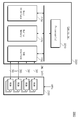
도 1은 본 발명의 실시 예에 따른 비휘발성 메모리 장치를 예시적으로 보여주는 도면이다.
도 2는 도 1에 도시된 비휘발성 메모리 장치의 프로그램 동작을 개략적으로 설명하기 위한 도면이다.
도 3은 도 1에 도시된 비휘발성 메모리 장치의 프로그램 방법에 대한 실시 예를 보여주는 흐름도이다.
도 4는 도 1에 도시된 비휘발성 메모리 장치의 읽기 동작을 개략적으로 설명하기 위한 도면이다.
도 5는 본 발명의 실시 예에 따른 비휘발성 메모리 장치의 읽기 방법을 예시적으로 보여주는 흐름도이다.
도 6은 본 발명의 다른 실시 예에 따른 메모리 장치를 예시적으로 보여주는 도면이다.
도 7은 본 발명에 따른 메모리 시스템을 예시적으로 보여주는 블록도이다.
도 8은 본 발명의 실시 예에 따른 SSD를 예시적으로 보여주는 블록도이다.
도 9는 본 발명에 따른 eMMC를 예시적으로 보여주는 블록도이다.1 is an exemplary illustration of a non-volatile memory device according to an embodiment of the present invention.
FIG. 2 is a diagram for schematically explaining a program operation of the nonvolatile memory device shown in FIG.
3 is a flowchart showing an embodiment of a programming method of the nonvolatile memory device shown in FIG.
FIG. 4 is a schematic view for explaining a read operation of the nonvolatile memory device shown in FIG. 1. Referring to FIG.
5 is a flowchart illustrating an exemplary method of reading a non-volatile memory device according to an embodiment of the present invention.
6 is an exemplary illustration of a memory device according to another embodiment of the present invention.
7 is a block diagram illustrating an exemplary memory system in accordance with the present invention.
8 is a block diagram illustrating an SSD according to an exemplary embodiment of the present invention.
9 is a block diagram illustrating an exemplary eMMC according to the present invention.
아래에서는 도면들을 이용하여 본 발명의 기술 분야에서 통상의 지식을 가진 자가 용이하게 실시할 수 있을 정도로 본 발명의 내용을 명확하고 상세하게 기재할 것이다.BRIEF DESCRIPTION OF THE DRAWINGS The above and other objects, features and advantages of the present invention will be more apparent from the following detailed description taken in conjunction with the accompanying drawings, in which: FIG.
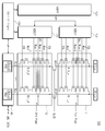
도 1은 본 발명의 실시 예에 따른 비휘발성 메모리 장치(100)를 예시적으로 보여주는 도면이다. 도 1을 참조하면, 비휘발성 메모리 장치(100)는 제 1 및 제 2 메모리 블록들(111, 122)로 구성된 메모리 셀 어레이(110), 전압 발생 회로(120, VGNRT), 제 1 및 제 2 어드레스 디코더들(131, 132, XDEC), 입출력 회로(140), 및 제어 로직(150)을 포함한다.1 is an exemplary illustration of a
본 발명의 실시 예에 따른 비휘발성 메모리 장치(100)는 낸드 플래시 메모리(NAND Flash Memory), 수직형 낸드 플래시 메모리(Vertical NAND, 이하, 'VNAND'라고 함), 노아 플래시 메모리(NOR Flash Memory), 저항성 램(Resistive Random Access Memory: RRAM), 상변화 메모리(Phase-Change Memory: PRAM), 자기저항 메모리(Magnetoresistive Random Access Memory: MRAM), 강유전체 메모리(Ferroelectric Random Access Memory: FRAM), 스핀주입 자화반전 메모리(Spin Transfer Torque Random Access Memory: STT-RAM) 등이 될 수 있다.A
또한, 본 발명의 비휘발성 메모리 장치는 3차원 어레이 구조(three-dimensional array structure)로 구현될 수 있다. 본 발명은 전하 저장층이 전도성 부유 게이트로 구성된 플래시 메모리 장치는 물론, 전하 저장층이 절연막으로 구성된 차지 트랩형 플래시(charge trap flash; CTF)에도 모두 적용 가능하다. 아래에서는 설명의 편의를 위하여 비휘발성 메모리 장치(100)가 낸드 플래시 메모리 장치라고 하겠다.In addition, the non-volatile memory device of the present invention may be implemented as a three-dimensional array structure. The present invention is applicable not only to a flash memory device in which the charge storage layer is made of a conductive floating gate but also to a charge trap flash (CTF) in which the charge storage layer is made of an insulating film. Hereinafter, the
메모리 셀 어레이(110)는 복수의 메모리 블록들을 포함한다. 도 1에서는 설명의 편의를 위하여 두 개의 메모리 블록들(111, 112)을 도시한다. 메모리 블록들(111, 112) 각각은, 비트라인들(BL0 ~ BLn, n은 2이상의 정수) 각각에 연결된 스트링(string)을 포함한다. 여기서 비트라인들(BL0 ~ BLn) 각각은 상부 비트라인들(BL0_u ~ BLn_u), 하부 비트라인들(BL0_d ~ BLn_u), 상부 비트라인들(BL0_u ~ BLn_u)과 하부 비트라인들(BL0_d ~ BLn_u)을 비트라인 공유 신호(BLSS)에 응답하여 연결하는 비트라인 공유 트랜지스터들(BST0 ~ BSTn)로 구성된다.The memory cell array 110 includes a plurality of memory blocks. In FIG. 1, two
실시 예에 있어서, 상부 비트라인들(BL0_u ~ BLn_u)은 제 1 메모리 블록(111)에 연결되고, 하부 비트라인들(BL0_d ~ BLn_u)은 제 2 메모리 블록(112)에 연결될 것이다. 도 1에 도시되지 않았지만, 상부 비트라인들(BL0_u ~ BLn_u)에는 복수의 메모리 블록들이 연결되고, 하부 비트라인들(BL0_d ~ BLn_u)에는 복수의 메모리 블록들이 연결될 것이다.The upper bit lines BL0_u to BLn_u may be coupled to the
실시 예에 있어서, 비트라인 공유 트랜지스터(BST0 ~ BSTn)의 게이트들은 비트라인 공유 신호(BLSS)를 입력 받는다.In the embodiment, gates of the bit line sharing transistors BST0 to BSTn receive the bit line sharing signal BLSS.
실시 예에 있어서, 비트라인 공유 트랜지스터(BST0 ~ BSTn) 각각은 고전압용 트랜지스터일 수 있다.In the embodiment, each of the bit line sharing transistors BST0 to BSTn may be a high voltage transistor.
여기서 스트링은 직렬 연결된 적어도 하나의 스트링 선택 트랜지스터(SST), 메모리 셀들(MC0 ~ MCm, m은 2 이상의 정수), 적어도 하나의 접지 선택 트랜지스터(GST)를 포함한다. 스트링 선택 트랜지스터(SST)는 스트링 선택 라인(SSL)을 통하여 전송되는 전압에 의하여 구동된다. 접지 선택 트랜지스터(GST)는 접지 선택 라인(GSL)을 통하여 전송되는 전압에 의하여 구동된다. 메모리 셀들(MC0 ~ MCm) 각각은 적어도 하나의 비트의 데이터를 저장하고, 대응하는 워드라인들(WL0 ~ WLm)에 전송되는 전압들에 의하여 구동된다.Wherein the string comprises at least one string selection transistor (SST) connected in series, memory cells (MC0 to MCm, m is an integer greater than one) and at least one ground selection transistor (GST). The string selection transistor (SST) is driven by a voltage transmitted through a string selection line (SSL). The ground selection transistor GST is driven by the voltage transmitted through the ground selection line GSL. Each of the memory cells MC0 to MCm stores at least one bit of data and is driven by voltages transferred to the corresponding word lines WL0 to WLm.
전압 발생 회로(120)는 비휘발성 메모리 장치(100)의 구동에 필요한 구동 전압들(Vpp, Vers, Vpgm, Vpass, Vr, Vread, ...)을 발생한다. 전압 발생 회로(120)는 적어도 하나의 전하 펌프(도시되지 않음)를 이용하거나 외부 고전압을 분배함으로써 구동 전압들을 발생할 수 있다.The
제 1 및 제 2 어드레스 디코더들(131, 132) 각각은 어드레스에 응답하여 복수의 메모리 블록들 중 어느 하나를 선택하고, 구동에 필요한 워드라인 전압들(예를 들어, 프로그램 전압(Vpgm), 패스 전압(Vpass), 소거 전압(Vers), 검증 전압(Vvfy, 읽기 전압(Vr), 읽기 패스 전압(Vread) 등)을 대응하는 워드라인들로 전송한다. 또한 제 1 및 제 2 어드레스 디코더들(131, 132) 각각은 프로그램 동작 혹은 읽기 동작시 입력된 어드레스를 근거로 하여 워드라인을 선택할 수 있다. 도 1에 도시되지 않았지만, 어드레스 디코터들의 개수는 메모리 블록들의 개수에 일대일로 대응될 것이다.Each of the first and
입출력 회로(140)는 프로그램 동작에서 외부로부터 입력된 2 워드라인 데이터(2 WL data)를 임시로 저장하였다가 쓰여질 페이지들(1st Page, 2nd Page)에 저장하거나, 읽기 동작에서 읽혀질 페이지들(1st Page, 2nd Page)로부터 2 워드라인 데이터를 읽어와 임시로 저장하였다가 외부로 출력한다. 여기서 페이지들(1st Page, 2nd Page) 각각은 하나의 워드라인(예를 들어, WLm-1)에 연결된 메모리 셀들을 의미한다.The input /
또한, 입출력 회로(140)는 비트라인들(BL0 ~ BLn) 각각에 대응하는 페이지 버퍼들(PB0 ~ PBn)을 포함한다. 페이지 버퍼들(PB0 ~ PBn) 각각은, 프로그램/읽기 동작의 위하여 복수의 데이터 래치들(도시되지 않음), 상부 감지 래치들(SL0_u ~ SLn_u), 및 하부 감지 래치들(SL0_d ~ SLn_d)을 포함한다.In addition, the input /
실시 예에 있어서, 복수의 데이터 래치들은 프로그램 동작 혹은 읽기 동작시 입출력되는 2 워드라인 데이터를 저장할 것이다.In an embodiment, the plurality of data latches will store 2 word line data that is input / output in a program operation or a read operation.
실시 예에 있어서, 상부 감지 래치들(SL0_u ~ SLn_u) 각각은 메모리 셀 어레이(100)의 상부에 배치되고 상부 비트라인들(BL0_u ~ BLn_u)에 연결될 것이다.In an embodiment, each of the upper sensing latches SL0_u to SLn_u may be disposed on top of the
실시 예에 있어서, 하부 감지 래치들(SL0_d ~ SLn_d) 각각은 메모리 셀 어레이(100)의 하부에 배치되고, 하부 비트라인들(BL0_d ~ BLn_d)에 연결될 것이다.In the embodiment, each of the lower sense latches SL0_d to SLn_d is disposed below the
제어 로직(150)은 비휘발성 메모리 장치(100)의 전반적인 동작을 제어한다. 제어 로직(150)은 외부의 메모리 제어기로부터 제공되는 제어 신호들 및 명령을 해석하고, 해석 결과에 응답하여 전압 발생 회로(120), 어드레스 디코더들(131, 132), 및 입출력 회로(140)를 제어한다.The
실시 예에 있어서, 제어 로직(150)은 프로그램 동작 혹은 읽기 동작시 2개의 워드라인들(예를 들어, WL1, WLm-1)에 연결된 제 1 및 제 2 페이지들로/로부터 2 워드라인 데이터를 동시에 쓰거나 혹은 읽을 수 있도록 전압 발생 회로(120), 어드레스 디코더들(131, 132), 및 입출력 회로(140)를 제어할 수 있다.In an embodiment, the
실시 예에 있어서, 제어 로직(150)은 제 1 및 제 2 페이지들로/로부터 동시에 프로그램/읽기 동작을 수행하기 위하여 비트라인 공유 신호(BLSS)를 발생할 것이다.In an embodiment,
본 발명의 실시 예에 따른 비휘발성 메모리 장치(100)는, 비트라인들(BL0 ~ BLn)을 분리함으로써 동시에 2개의 워드라인들에 연결된 페이지들로/로부터 데이터를 쓰거나 읽을 수 있다. 그 결과로써, 본 발명의 실시 예에 따른 비휘발성 메모리 장치(100)는 종래의 그것과 비교하여 프로그램/읽기 동작의 성능을 크게 향상시킬 수 있다.The
또한, 본 발명의 실시 예에 따른 비휘발성 메모리 장치(100)는 데이터 감지 동작과 관련된 상부 감지 래치들(SL0_u ~ SLn_u)을 메모리 셀 어레이(110)의 상부에 배치시키고, 그 외의 페이지 버퍼들(PB0 ~ PBn)의 구성들은 메모리 셀 어레이(110)의 하부에 배치시킴으로써, 2 워드라인 데이터의 프로그램/읽기 동작에 대한 칩 사이즈 오버헤드를 줄일 수 있다.The
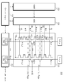
도 2는 도 1에 도시된 비휘발성 메모리 장치(100)의 프로그램 동작을 개략적으로 설명하기 위한 도면이다. 도 1 및 도 2를 참조하면, 프로그램 동작은 다음과 같이 진행된다. 외부로 2 워드라인 데이터를 입력 받고, 2 워드라인 데이터 중에서 제 1 페이지 데이터에 대응하는 전압들이 비트라인들(BL0 ~ BLn)에 인가된다(①). 이후, 비트라인 선택 트랜지스터들(BST0 ~ BSTn)이 턴-오프된다(②). 따라서 비트라인들(BL0 ~ BLn)의 상부 비트라인들(BL0_u ~ BLn_u)이 설정될 것이다. 이후, 하부 비트라인들(BL0_d ~ BLn_d)이 디스차지시키고 2 워드라인 데이터 중에서 제 2 페이지 데이터에 대응하는 전압들이 비트라인들(BL0 ~ BLn)에 인가된다(③). 따라서하부 비트라인들(BL0_d ~ BLn_d)이 설정될 것이다. 이후, 어드레스 디코더들(131, 132) 각각에 위해 선택된 워드라인으로 프로그램 전압이 인가될 것이다(④).FIG. 2 is a diagram for schematically explaining the program operation of the
본 발명의 실시 예에 따른 프로그램 동작은 제 1 페이지 데이터 및 제 2 페이지 데이터를 동시에 프로그램할 수 있다.The program operation according to the embodiment of the present invention can simultaneously program the first page data and the second page data.
도 3은 도 1에 도시된 비휘발성 메모리 장치(100)의 프로그램 방법에 대한 실시 예를 보여주는 흐름도이다. 도 1 내지 도 3을 참조하면, 비휘발성 메모리 장치(100)의 프로그램 방법은 다음과 같다.FIG. 3 is a flow chart showing an embodiment of a programming method of the
프로그램 동작시 프로그램될 2 워드라인 데이터가 데이터 입출력 회로(140)를 통하여 페이지 버퍼들(PB0 ~ PBn)에 로딩된다(S110). 전압 발생 회로(120)는 제어 로직(150)의 제어에 따라 프로그램 동작에 필요한 구동 전압들(예를 들어, 프로그램 전압, 패스 전압, 고전압, 웰전압, 검증읽기 전압 등)을 발생할 것이다.In the program operation, two word line data to be programmed are loaded into the page buffers PB0 to PBn through the data input / output circuit 140 (S110). The
이후, 페이지 버퍼들(PB0 ~ PBn)에 로딩된 데이터에 따라 상부 비트라인들(BL0_u ~ BLn_u) 및 하부 비트라인들(BL0_d ~ BLn_d)이 설정될 것이다. 도 1에 도시된 바와 같이, 비트라인 공유 트랜지스터들(BST0 ~ BSTn)을 턴온시킴으로써 제 1 페이지에 쓰여질 하나의 워드라인에 대응하는 데이터에 대응하여 상부 비트라인들(BL0_u ~ BLn_u)이 설정될 것이다. 이후, 비트라인 공유 트랜지스터들(BST0 ~ BSTn)을 턴오프시킴으로써 제 2 페이지에 쓰여질 하나의 워드라인에 대응하는 데이터에 대응하여 하부 비트라인들(BL0_d ~ BLn_d)이 설정될 것이다(S120).The upper bit lines BL0_u to BLn_u and the lower bit lines BL0_d to BLn_d will then be set according to the data loaded in the page buffers PB0 to PBn. As shown in Fig. 1, by turning on the bit line shared transistors BST0 to BSTn, the upper bit lines BL0_u to BLn_u are set corresponding to data corresponding to one word line to be written to the first page . Subsequently, by turning off the bit line sharing transistors BST0 to BSTn, the lower bit lines BL0_d to BLn_d will be set corresponding to the data corresponding to one word line to be written to the second page (S120).
어드레스 디코더들(131, 132) 각각은 어드레스를 근거로 하여 프로그램될 제 1 페이지 및 제 2 페이지에 대응하는 2개의 워드라인들(WLm-1)을 선택할 것이다(S130). 도 1에서는 설명의 편의를 위하여 선택된 워드라인(WLm-1)이 모두 m-1 번째 워드라인이었다. 하지만 본 발명의 어드레스 디코더들(131, 132)이 모두 동일한 위치(워드라인 순서에 있어서)의 워드라인을 선택한다고 제한될 필요는 없다. 어드레스 디코더들(131, 132) 각각은 입력 어드레스에 따라 어느 하나의 서로 다른 위치(워드라인 순서에 있어서)의 워드라인을 선택할 수 있다.Each of the
선택된 워드라인들(WLm-1)으로 프로그램 전압에 대응하는 프로그램 펄스가 인가되고, 비선택된 워드라인들(WL0 ~ WL2 ~ WLm-2, WLm)으로 패스 전압이 인가될 것이다. 프로그램 루프는 설정된 상부 비트라인들(BL0_u ~ BLn_u)을 근거로 한 제 1 프로그램 동작과 설정된 하부 비트라인들(BL0_d ~ BLn_d)을 근거로 한 제 2 프로그램 동작으로 구분될 것이다. 제 1 프로그램 동작과 제 2 프로그램 동작은 동시에 수행될 것이다.A program pulse corresponding to the program voltage is applied to the selected word lines WLm-1 and a pass voltage is applied to the unselected word lines WL0 to WL2 to WLm-2, WLm. The program loop will be divided into a first program operation based on the set upper bit lines BL0_u to BLn_u and a second program operation based on the set lower bit lines BL0_d to BLn_d. The first program operation and the second program operation will be performed simultaneously.
이후, 프로그램 검증 동작이 수행될 것이다. 여기서 프로그램 검증 동작은 아래에서 상술 된 읽기 동작과 유사하기 때문에 여기서는 설명을 생략하도록 하겠다. 프로그램 검증 동작이 패스이면 프로그램 동작은 완료될 것이다(S150). 반면에, 프로그램 검증 동작이 패스되지 않으면, 프로그램 루프 회수가 최대인지 판별한다(S160). 프로그램 루프 회수가 최대이면, 프로그램 동작은 실패한 것으로 처리될 것이다. 반면에, 프로그램 루프 회수가 최대가 아니라면, 프로그램 루프 회수는 증가되고, 프로그램 전압에 대응하는 프로그램 펄스의 레벨도 소정의 값만큼 증가되고, S140 단계로 진입될 것이다(S170).Thereafter, a program verify operation will be performed. Here, since the program verify operation is similar to the read operation described below, a description thereof will be omitted here. If the program verify operation is a pass, the program operation will be completed (S150). On the other hand, if the program verification operation is not passed, it is determined whether the program loop count is the maximum (S160). If the program loop count is the maximum, the program operation will be treated as failed. On the other hand, if the program loop count is not the maximum, the program loop count is increased, and the level of the program pulse corresponding to the program voltage is also increased by a predetermined value, and the process proceeds to step S140 (S170).
본 발명의 실시 예에 따른 비휘발성 메모리 장치(100)의 프로그램 방법은, 프로그램 루프마다 선택된 2개의 워드라인들에 동시에 프로그램 펄스를 인가할 것이다. The programming method of the
도 4는 도 1에 도시된 비휘발성 메모리 장치(100)의 읽기 동작을 개략적으로 설명하기 위한 도면이다. 도 1 및 도 4를 참조하면, 읽기 동작은 다음과 같이 진행된다. 프리차지 전압들이 비트라인들(BL0 ~ BLn)에 인가된다(①). 이후, 비트라인 선택 트랜지스터들(BST0 ~ BSTn)이 턴-오프된다(②). 이로써, 상부 비트라인들(BL0_u ~ BLn_u) 및 하부 비트라인들(BL0_d ~ BLn_d)이 프리차지될 것이다. 이후, 선택된 워드라인들(WLm-1, 도 1 참조)로 읽기 펄스가 동시에 인가될 것이다(③). 이후, 상부 비트라인들(BL0_u ~ BLn_u)의 전압들을 감지함으로써 제 1 페이지 데이터가 상부 감지 래치들(SL0_u ~ SLn_u)에 저장되고, 하부 비트라인들(BL0_d ~ BLn_d)의 전압들을 감지함으로써 제 2 페이지 데이터가 하부 감지 래치들(SL0_d ~ SLn_d)에 저장될 것이다(④).4 is a schematic diagram for explaining a read operation of the
본 발명의 실시 예에 따른 읽기 동작은 제 1 페이지 데이터 및 제 2 페이지 데이터를 동시에 읽을 수 있다.The read operation according to the embodiment of the present invention can simultaneously read the first page data and the second page data.
도 5는 본 발명의 실시 예에 따른 비휘발성 메모리 장치(100)의 읽기 방법을 예시적으로 보여주는 흐름도이다. 도 1, 도 4 및 도 5를 참조하면, 비휘발성 메모리 장치의 읽기 방법은 다음과 같다.5 is a flowchart illustrating an exemplary method of reading a
페이지 버퍼들(PB0 ~ PBn)은 읽기 동작시 비트라인 공유 트랜지스터들(BST0 ~ BSTn)을 턴온시킨 상태에서 상부 비트라인들(BL0_u ~ BLn_u) 및 하부 비트라인들(BL0_d ~ BLn_d)을 프리차지 시킨다(S210). 이후, 감지 동작을 위하여 비트라인 공유 트랜지스터들(BST0 ~ BSTn)을 턴오프시킨다. 이로써, 상부 비트라인들(BL0_u ~ BLn_u) 및 하부 비트라인들(BL0_d ~ BLn_d)이 모두 프리차지될 것이다.The page buffers PB0 to PBn precharge the upper bit lines BL0_u to BLn_u and the lower bit lines BL0_d to BLn_d with the bit line sharing transistors BST0 to BSTn turned on during a read operation (S210). Thereafter, the bit line sharing transistors BST0 to BSTn are turned off for the sensing operation. Thus, the upper bit lines BL0_u to BLn_u and the lower bit lines BL0_d to BLn_d will all be precharged.
이후, 어드레스 디코더들(131, 1320)은 어드레스를 근거로 하여 읽혀질 제 1 페이지 및 제 2 페이지에 대응하는 2개의 워드라인들(WLm-1)을 선택할 것이다(S220). 선택된 워드라인들로 읽기 전압이 인가될 것이다(S230). 감지 동작은 프리차지된 상부 비트라인들(BL0_u ~ BLn_u)을 이용하는 제 1 감지 동작과 프리차지된 하부 비트라인들(BL0_d ~ BLn_d)을 이용하는 제 2 감지 동작으로 구분될 것이다. 제 1 감지 동작 및 제 2 감지 동작은 동시에 수행될 것이다.Thereafter, the
이후, 상부 감지 래치들(SL0_u ~ SLn_u) 및 하부 감지 래치들(SL0_d ~ SLn_d)에 감지된 데이터에 대응하는 데이터를 페이지 버퍼들(PB0 ~ PBn)의 데이터 래치들에 저장할 것이다(S250). 여기서 데이터 래치들에 저장된 데이터는 2 워드라인 데이터일 것이다. 이후, 입출력 회로(140)는 읽혀진 2 워드라인 데이터를 출력할 것이다(S260).The data corresponding to the sensed data in the upper sensing latches SL0_u to SLn_u and the lower sensing latches SL0_d to SLn_d will be stored in the data latches of the page buffers PB0 to PBn at step S250. Where the data stored in the data latches will be two word line data. Then, the input /
본 발명의 실시 예에 따른 비휘발성 메모리 장치(100)의 읽기 방법은 2개의 워드라인들에 연결된 메모리 셀들로부터 동시에 데이터를 읽을 수 있다.A method of reading a
도 1 내지 도 5에서는 어드레스 디코더들(131, 132) 각각이 프로그램 동작 혹은 읽기 동작시 하나의 워드라인을 선택한다. 그러나 본 발명이 반드시 여기에 제한될 필요는 없다. 어드레스 디코더는 두 개의 워드라인들을 선택하도록 구현될 수도 있다.1 to 5, each of the
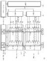
도 6은 본 발명의 다른 실시 예에 따른 메모리 장치(200)를 예시적으로 보여주는 도면이다. 도 6을 참조하면, 메모리 장치(200)는 메모리 셀 어레이(210), 전압 발생 회로(220, VGNRT), 어드레스 디코더(230, XDEC), 입출력 회로(240), 및 제어 로직(250)을 포함한다.Figure 6 is an exemplary illustration of a
메모리 셀 어레이(110)는 복수의 메모리 블록들을 포함한다. 도 5에서는 설명의 편의를 위하여 하나의 메모리 블록을 도시한다. 메모리 블록은, 비트라인들(BL0 ~ BLn, n은 2이상의 정수) 각각에 연결된 스트링(string)을 포함한다. 여기서 비트라인들(BL0 ~ BLn) 각각은 상부 비트라인들(BL0_u ~ BLn_u), 하부 비트라인들(BL0_d ~ BLn_u), 상부 비트라인들(BL0_u ~ BLn_u)과 하부 비트라인들(BL0_d ~ BLn_u)을 비트라인 공유 신호(BLSS)에 응답하여 연결하는 비트라인 공유 트랜지스터들(BST0 ~ BSTn)로 구성된다. 비트라인 공유 트랜지스터(BST0 ~ BSTn)의 게이트들은 비트라인 공유 신호(BLSS)를 입력 받는다. 여기서 스트링은 직렬 연결된 적어도 하나의 스트링 선택 트랜지스터(SST), 메모리 셀들(MC0 ~ MCm, m은 2 이상의 정수), 적어도 하나의 접지 선택 트랜지스터(GST)를 포함한다. The memory cell array 110 includes a plurality of memory blocks. In FIG. 5, one memory block is shown for convenience of explanation. The memory block includes a string connected to each of the bit lines (BL0 to BLn, where n is an integer of 2 or more). Each of the bit lines BL0 to BLn includes upper bit lines BL0_u to BLn_u, lower bit lines BL0_d to BLn_u, upper bit lines BL0_u to BLn_u and lower bit lines BL0_d to BLn_u, Bit line sharing transistors (BST0 to BSTn) for connecting bit lines in response to a bit line sharing signal (BLSS). The gates of the bit line sharing transistors BST0 to BSTn receive the bit line sharing signal BLSS. Wherein the string comprises at least one string selection transistor (SST) connected in series, memory cells (MC0 to MCm, m is an integer greater than one) and at least one ground selection transistor (GST).
전압 발생 회로(220)는 비휘발성 메모리 장치(200)의 구동에 필요한 구동 전압들(Vpp, Vers, Vpgm, Vpass, Vr, Vread, ...)을 발생한다. 전압 발생 회로(220)는 적어도 하나의 전하 펌프(도시되지 않음)를 이용하거나 외부 고전압을 분배함으로써 구동 전압들을 발생할 수 있다.The
어드레스 디코더(230)는 프로그램 동작 혹은 읽기 동작시 입력된 어드레스를 근거로 하여 워드라인들(WL0 ~ WLm) 중 두 개를 선택할 수 있다.The
입출력 회로(240)는 프로그램 동작에서 외부로부터 입력된 2 워드라인 데이터(2 WL data)를 임시로 저장하였다가 쓰여질 페이지들(1st Page, 2nd Page)에 저장하거나, 읽기 동작에서 읽혀질 페이지들(1st Page, 2nd Page)로부터 2 워드라인 데이터를 읽어와 임시로 저장하였다가 외부로 출력한다. 여기서 페이지들(1st Page, 2nd Page) 각각은 하나의 워드라인에 연결된 메모리 셀들을 의미한다.The input /
또한, 입출력 회로(240)는 비트라인들(BL0 ~ BLn) 각각에 대응하는 페이지 버퍼들(PB0 ~ PBn)을 포함한다. 페이지 버퍼들(PB0 ~ PBn) 각각은, 프로그램/읽기 동작의 위하여 복수의 데이터 래치들(도시되지 않음), 상부 감지 래치들(SL0_u ~ SLn_u), 및 하부 감지 래치들(SL0_d ~ SLn_d)을 포함한다.The input /
제어 로직(250)은 비휘발성 메모리 장치(200)의 전반적인 동작을 제어한다. 제어 로직(250)은 외부의 메모리 제어기로부터 제공되는 제어 신호들 및 명령을 해석하고, 해석 결과에 응답하여 전압 발생 회로(220), 어드레스 디코더(230), 및 입출력 회로(240)를 제어한다.The
실시 예에 있어서, 제어 로직(250)은 프로그램 동작 혹은 읽기 동작시 2개의 워드라인들(예를 들어, WL1, WLm-1)에 연결된 제 1 및 제 2 페이지들로/로부터 2 워드라인 데이터를 동시에 쓰거나 혹은 읽을 수 있도록 전압 발생 회로(120), 어드레스 디코더(240), 및 입출력 회로(240)를 제어할 수 있다.In an embodiment, the
실시 예에 있어서, 제어 로직(250)은 제 1 및 제 2 페이지들로/로부터 동시에 프로그램/읽기 동작을 수행하기 위하여 비트라인 공유 신호(BLSS)를 발생할 것이다.In an embodiment, the
도 7은 본 발명에 따른 메모리 시스템을 예시적으로 보여주는 블록도이다. 도 7을 참조하면, 메모리 시스템(1000)은 적어도 하나의 비휘발성 메모리 장치(1100) 및 메모리 제어기(1200)를 포함한다. 비휘발성 메모리 장치(1100)는 도 1 및 도 6에서 설명된 비휘발성 메모리 장치들(100, 200) 중 어느 하나로 구현될 것이다. 즉, 비휘발성 메모리 장치(1100)는 2 워드라인 데이터 단위로 프로그램 동작을 수행하거나 읽기 동작을 수행할 수 있다.7 is a block diagram illustrating an exemplary memory system in accordance with the present invention. Referring to FIG. 7,
메모리 제어기(1200)는 복수의 채널들을 통하여 비휘발성 메모리 장치(1100)에 연결된다. 메모리 제어기(1200)는 적어도 하나의 프로세서(1210), 버퍼 메모리(1220), 에러 정정회로(1230), 코드 메모리(1240), 호스트 인터페이스(1250) 및 메모리 인터페이스(1260)를 포함한다.
본 발명의 실시 예에 따른 메모리 시스템(1000)은, 2 워드라인 데이터 단위로 입출력함으로써, 비휘발성 메모리 장치(1100)의 프로그램/읽기 성능을 향상시킨다.The
본 발명은 SSD(solid state drive)에 적용 가능하다.The present invention is applicable to a solid state drive (SSD).
도 8은 본 발명의 실시 예에 따른 SSD를 예시적으로 보여주는 블록도이다. 도 8을 참조하면, SSD(2000)는 복수의 플래시 메모리 장치들(2100) 및 SSD 제어기(2200)를 포함한다. 플래시 메모리 장치들(2100)은 외부 고전압(Vpp)을 제공받도록 구현될 수 있다. 플래시 메모리 장치들(2100) 각각은 도 1 내지 도 6에 설명된 2 워드라인 데이터 단위로 프로그램 동작과 읽기 동작을 수행하도록 구현될 것이다. SSD 제어기(2200)는 복수의 채널들(CH1~CHi, i는 2 이상의 정수)을 통하여 플래시 메모리 장치들(2100)에 연결된다. SSD 제어기(2200)는 적어도 하나의 중앙처리장치(2210), 버퍼 메모리(2220), 호스트 인터페이스(2250) 및 플래시 인터페이스(2260)를 포함한다.8 is a block diagram illustrating an SSD according to an exemplary embodiment of the present invention. Referring to FIG. 8, the
본 발명에 따른 SSD(2000)는 프로그램 동작 및 읽기 동작시 2 워드라인 데이터 단위로 구동됨으로써, 대용량 데이터를 저장하는데 유리하다.The
본 발명은 eMMC(embedded)에 적용 가능하다.The present invention is applicable to eMMC (embedded).
도 9는 본 발명에 따른 eMMC를 예시적으로 보여주는 블록도이다. 도 9를 참조하면, eMMC(3000)는 적어도 하나의 낸드 플래시 메모리 장치(3100) 및 제어기(3200)를 포함할 수 있다. 낸드 플래시 메모리 장치(3100)는 SDR(single data rate) 낸드 혹은 DDR(double data rate) 낸드, toggle NAND일 수 있다. 실시 예에 있어서, 낸드 플래시 메모리 장치(3100)는 단품의 낸드 플래시 메모리 장치들을 포함할 수 있다. 여기서, 단품의 낸드 플래시 메모리 장치들은 하나의 패키지(예를 들어, FBGA, Fine-pitch Ball Grid Array)에 적층 되어 구현될 수 있다. 여기서 낸드 플래시 메모리 장치들 각각은, 도 1 내지 도 6에서 설명된 구동 방법으로 구현될 것이다.9 is a block diagram illustrating an exemplary eMMC according to the present invention. Referring to FIG. 9, the
메모리 제어기(3200)는 복수의 채널들을 통하여 플래시 메모리 장치(3100)에 연결된다. 제어기(3200)는 적어도 하나의 제어기 코어(3210), 호스트 인터페이스(3250) 및 낸드 인터페이스(3260)를 포함한다. 적어도 하나의 제어기 코어(3210)는 eMMC(3000)의 전반적인 동작을 제어한다. 호스트 인터페이스(3250)는 제어기(3210)와 호스트의 인터페이싱을 수행한다. 낸드 인터페이스(3260)는 낸드 플래시 메모리 장치(3100)와 제어기(3200)의 인터페이싱을 수행한다. 실시 예에 있어서, 호스트 인터페이스(3250)는 병렬 인터페이스(예를 들어, MMC 인터페이스)일 수 있다. 다른 실시 예에 있어서, eMMC(3000)의 호스트 인터페이스(3250)는 직렬 인터페이스(예를 들어, UHS-II, UFS 인터페이스)일 수 있다.The
eMMC(3000)는 호스트로부터 전원 전압들(Vcc, Vccq)을 제공받는다. 여기서, 제 1 전원 전압(Vcc: 3.3V)은 낸드 플래시 메모리 장치(3100) 및 낸드 인터페이스(3230)에 제공되고, 제 2 전원 전압(Vccq: 1.8V/3.3V)은 제어기(3200)에 제공된다.The
본 발명의 실시 예에 따른 eMMC(3000)는 소형 및 저전력이 요구되는 모바일 제품(예를 들어, 갤럭시S 시리즈, 갤럭시노트 시리즈, 아이폰, 아이패드, 넥서스, 패블릿(Phablit) 등)에 응용 가능하다.The
한편, 상술 된 본 발명의 내용은 발명을 실시하기 위한 구체적인 실시 예들에 불과하다. 본 발명은 구체적이고 실제로 이용할 수 있는 수단 자체뿐 아니라, 장차 기술로 활용할 수 있는 추상적이고 개념적인 아이디어인 기술적 사상을 포함할 것이다.The above-described contents of the present invention are only specific examples for carrying out the invention. The present invention will include not only concrete and practical means themselves, but also technical ideas which are abstract and conceptual ideas that can be utilized as future technologies.
100: 비휘발성 메모리 장치
110: 메모리 셀 어레이
120: 전압 발생 회로
130: 어드레스 디코더
140: 입출력 회로
150: 제어 로직
PB0 ~ PBn: 페이지 버퍼
SL0_u ~ SLn_u: 상부 감지 래치
SL0_d ~ SLn_d: 하부 감지 래치
BST0 ~ BSTn: 비트라인 공유 트랜지스터
BLSS: 비트라인 공유 신호
BL0_u ~ BLn_u: 상부 비트라인
BL0_d ~ BLn_d: 하부 비트라인
WL0 ~ WLm: 워드라인100: Nonvolatile memory device
110: memory cell array
120: Voltage generating circuit
130:
140: input / output circuit
150: control logic
PB0 to PBn: Page buffer
SL0_u ~ SLn_u: upper sense latch
SL0_d ~ SLn_d: Lower sense latch
BST0 to BSTn: Bit line shared transistor
BLSS: bit line shared signal
BL0_u to BLn_u: upper bit line
BL0_d to BLn_d:
WL0 to WLm: word line
Claims (10)
제 1 워드라인에 연결된 제 1 메모리 셀들에 저장될 제 1 워드라인 데이터 및 제 2 워드라인에 연결된 제 2 메모리 셀들에 저장될 제 2 워드라인 데이터를 로딩하는 단계;
상기 제 1 워드라인 데이터에 따라 상부 비트라인들을 설정하는 단계;
상기 상부 비트라인들을 설정한 후, 비트라인 공유 트랜지스터들을 턴오프시키고 상기 제 2 워드라인 데이터에 따라 하부 비트라인들을 설정하는 단계;
상기 상부 비트라인들의 전압들을 이용하여 상기 제 1 메모리 셀들에 제 1 프로그램 동작을 수행하는 단계;
상기 비트라인 공유 트랜지스터들을 턴온시키고 상기 하부 비트라인들의 전압들을 이용하여 상기 제 2 메모리 셀들에 제 2 프로그램 동작을 수행하는 단계를 포함하고,
상기 비트라인 공유 트랜지스터들은 비트라인 공유 신호에 응답하여 상기 상부 비트라인들과 상기 하부 비트라인들을 전기적으로 연결하는 프로그램 방법.A method of programming a non-volatile memory device comprising:
Loading first word line data to be stored in first memory cells connected to a first word line and second word line data to be stored in second memory cells connected to a second word line;
Setting upper bit lines according to the first word line data;
After setting the upper bit lines, turning off the bit line shared transistors and setting the lower bit lines according to the second word line data;
Performing a first programming operation on the first memory cells using voltages of the upper bit lines;
Turning on the bit line shared transistors and performing a second program operation on the second memory cells using voltages of the lower bit lines,
Wherein the bit line sharing transistors electrically connect the upper bit lines and the lower bit lines in response to a bit line shared signal.
상기 제 1 프로그램 동작을 수행하는 단계는,
상기 제 1 워드라인으로 프로그램 펄스를 인가하는 단계를 포함하고,
상기 제 2 프로그램 동작을 수행하는 단계는,
상기 제 2 워드라인으로 상기 프로그램 펄스를 인가하는 단계를 포함하는 프로그램 방법.The method according to claim 1,
Wherein the performing the first program operation comprises:
Applying a program pulse to the first word line,
Wherein the performing the second program operation comprises:
And applying the program pulse to the second word line.
상기 제 1 프로그램 동작 및 상기 제 2 프로그램 동작이 동시에 수행되는 프로그램 방법.3. The method of claim 2,
Wherein the first program operation and the second program operation are performed simultaneously.
상기 제 1 메모리 셀들이 포함된 제 1 메모리 블록과 상기 제 2 메모리 셀들이 포함된 제 2 메모리 블록은 서로 분리되는 프로그램 방법.The method according to claim 1,
Wherein the first memory block including the first memory cells and the second memory block including the second memory cells are separated from each other.
상기 제 1 및 제 2 프로그램 동작들을 수행한 뒤에 프로그램 검증 동작을 수행하는 단계를 더 포함하는 프로그램 방법.The method according to claim 1,
And performing a program verify operation after performing the first and second program operations.
상기 프로그램 검증 동작이 실패하면, 사전에 결정된 값만큼 프로그램 펄스를 증가시킨 후, 상기 상부 비트라인들 및 상기 하부 비트라인들을 설정하고, 상기 제 1 및 제 2 프로그램 동작들을 반복하는 단계를 더 포함하는 프로그램 방법. 6. The method of claim 5,
If the program verify operation fails, incrementing the program pulse by a predetermined value, then setting the upper bit lines and the lower bit lines, and repeating the first and second program operations How to program.
상기 비트라인 공유 트랜지스터들 각각은 고전압용 트랜지스터인 프로그램 방법.The method according to claim 1,
Each of the bit line shared transistors being a high voltage transistor.
비트라인 공유 트랜지스터들을 턴온시키고 상부 비트라인들과 하부 비트라인들을 프리차지시키는 단계;
상기 상부 비트라인들 및 상기 하부 비트라인들을 프리차지시킨 후, 상기 비트라인 공유 트랜지스터들을 턴오프시키는 단계;
어드레스에 응답하여 선택된 제 1 및 제 2 워드라인들로 읽기 전압을 인가하는 단계;
상기 상부 비트라인들에 연결된 상부 감지 래치들을 통하여 상기 제 1 워드라인들에 연결된 제 1 메모리 셀들의 데이터를 감지하는 제 1 감지 단계;
상기 비트라인 공유 트랜지스터들을 턴오프시키고 상기 하부 비트라인들에 연결된 하부 감지 래치들을 통하여 상기 제 2 워드라인들에 연결된 제 2 메모리 셀들의 데이터를 감지하는 제 2 감지 단계;
상기 상부 감지 래치들에 저장된 데이터 및 상기 하부 감지 래치들에 저장된 데이터에 대응하는 데이터를 데이터 래치들에 저장하는 단계; 및
상기 데이터 래치들에 저장된 데이터를 외부로 출력하는 단계를 포함하고,
상기 비트라인 공유 트랜지스터들은 비트라인 공유 신호에 응답하여 상기 상부 비트라인들과 상기 하부 비트라인들을 전기적으로 연결하는 읽기 방법. A method of reading a non-volatile memory device comprising:
Turning on the bit line shared transistors and precharging the upper bit lines and the lower bit lines;
Precharging the upper bit lines and the lower bit lines, and then turning off the bit line shared transistors;
Applying a read voltage to selected first and second word lines in response to an address;
A first sensing step of sensing data of first memory cells connected to the first word lines through upper sensing latches connected to the upper bit lines;
A second sensing step of sensing data of second memory cells connected to the second word lines through the lower sensing latches connected to the lower bit lines by turning off the bit line sharing transistors;
Storing data stored in the upper sensing latches and data corresponding to data stored in the lower sensing latches in data latches; And
And outputting the data stored in the data latches to the outside,
Wherein the bit line sharing transistors electrically connect the upper bit lines and the lower bit lines in response to a bit line sharing signal.
상기 비휘발성 메모리 장치는 제 1 및 제 2 메모리 셀들을 갖는 메모리 셀 어레이를 포함하고,
상기 상부 감지 래치들은 상기 메모리 셀 어레이의 상부에 배치되고,
상기 데이터 래치들 및 상기 하부 감지 래치들은 상기 메모리 셀 어레이의 하부에 배치되는 읽기 방법.9. The method of claim 8,
The non-volatile memory device comprising a memory cell array having first and second memory cells,
The upper sensing latches being disposed on top of the memory cell array,
Wherein the data latches and the lower sense latches are disposed below the memory cell array.
상기 상부 비트라인들 각각에 스트링이 연결되고,
상기 스트링은, 직렬 연결된 적어도 하나의 스트링 선택 트랜지스터, 복수의 메모리 셀들, 및 적어도 하나의 접지 선택 트랜지스터를 포함하는 읽기 방법.9. The method of claim 8,
A string is connected to each of the upper bit lines,
Wherein the string comprises at least one string selection transistor connected in series, a plurality of memory cells, and at least one ground selection transistor.
Priority Applications (3)
| Application Number | Priority Date | Filing Date | Title |
|---|---|---|---|
| KR1020130013033A KR20140100143A (en) | 2013-02-05 | 2013-02-05 | Programming and reading methods of nonvolatle memory device |
| US14/151,534 US9396797B2 (en) | 2013-02-05 | 2014-01-09 | Program methods of memory devices using bit line sharing |
| US15/188,461 US9633704B2 (en) | 2013-02-05 | 2016-06-21 | Read methods of memory devices using bit line sharing |
Applications Claiming Priority (1)
| Application Number | Priority Date | Filing Date | Title |
|---|---|---|---|
| KR1020130013033A KR20140100143A (en) | 2013-02-05 | 2013-02-05 | Programming and reading methods of nonvolatle memory device |
Publications (1)
| Publication Number | Publication Date |
|---|---|
| KR20140100143A true KR20140100143A (en) | 2014-08-14 |
Family
ID=51259102
Family Applications (1)
| Application Number | Title | Priority Date | Filing Date |
|---|---|---|---|
| KR1020130013033A KR20140100143A (en) | 2013-02-05 | 2013-02-05 | Programming and reading methods of nonvolatle memory device |
Country Status (2)
| Country | Link |
|---|---|
| US (2) | US9396797B2 (en) |
| KR (1) | KR20140100143A (en) |
Cited By (1)
| Publication number | Priority date | Publication date | Assignee | Title |
|---|---|---|---|---|
| US10121543B2 (en) | 2015-08-21 | 2018-11-06 | Samsung Electronics Co., Ltd. | Storage device including a nonvolatile memory device and a controller for controlling a write operation of the nonvolatile memory device and an operating method of the storage device |
Families Citing this family (10)
| Publication number | Priority date | Publication date | Assignee | Title |
|---|---|---|---|---|
| US8860117B2 (en) | 2011-04-28 | 2014-10-14 | Micron Technology, Inc. | Semiconductor apparatus with multiple tiers of memory cells with peripheral transistors, and methods |
| US8964474B2 (en) | 2012-06-15 | 2015-02-24 | Micron Technology, Inc. | Architecture for 3-D NAND memory |
| US9362300B2 (en) * | 2014-10-08 | 2016-06-07 | Micron Technology, Inc. | Apparatuses and methods for forming multiple decks of memory cells |
| KR102340328B1 (en) * | 2016-01-07 | 2021-12-16 | 에스케이하이닉스 주식회사 | Semiconductor memory device and operating method thereof |
| US9679650B1 (en) | 2016-05-06 | 2017-06-13 | Micron Technology, Inc. | 3D NAND memory Z-decoder |
| US10074430B2 (en) | 2016-08-08 | 2018-09-11 | Micron Technology, Inc. | Multi-deck memory device with access line and data line segregation between decks and method of operation thereof |
| KR102649347B1 (en) * | 2016-10-11 | 2024-03-20 | 삼성전자주식회사 | Method for programming non-volatile memory device and method for operating system having the same |
| KR20200141304A (en) * | 2019-06-10 | 2020-12-18 | 에스케이하이닉스 주식회사 | Semiconductor device and operating method of semiconductor device |
| US11450381B2 (en) | 2019-08-21 | 2022-09-20 | Micron Technology, Inc. | Multi-deck memory device including buffer circuitry under array |
| US11189335B2 (en) * | 2019-11-13 | 2021-11-30 | Sandisk Technologies Llc | Double write/read throughput by CMOS adjacent array (CaA) NAND memory |
Family Cites Families (14)
| Publication number | Priority date | Publication date | Assignee | Title |
|---|---|---|---|---|
| KR100948483B1 (en) | 2003-04-01 | 2010-03-18 | 주식회사 하이닉스반도체 | Semiconductor memory device |
| JP4654671B2 (en) | 2004-11-29 | 2011-03-23 | ソニー株式会社 | Semiconductor memory device |
| US7313023B2 (en) | 2005-03-11 | 2007-12-25 | Sandisk Corporation | Partition of non-volatile memory array to reduce bit line capacitance |
| KR100742278B1 (en) | 2005-11-23 | 2007-07-24 | 삼성전자주식회사 | Nand flash memory device with improved operating operation and dual program fucntion |
| EP1814123A1 (en) | 2006-01-26 | 2007-08-01 | Samsung Electronics Co.,Ltd. | Nand-type nonvolatile memory device having common bit lines and methods of operating the same |
| KR100666184B1 (en) * | 2006-02-02 | 2007-01-09 | 삼성전자주식회사 | Three-level nonvolatile semiconductor memory device with voltage control block shared lower bitlines and upper bitlines |
| JP2007293986A (en) | 2006-04-24 | 2007-11-08 | Toshiba Corp | Semiconductor memory device |
| KR100854972B1 (en) * | 2007-02-13 | 2008-08-28 | 삼성전자주식회사 | Memory system and data reading method thereof |
| US7706184B2 (en) | 2007-12-28 | 2010-04-27 | Kabushiki Kaisha Toshiba | Nonvolatile semiconductor memory device |
| KR101462606B1 (en) | 2008-10-08 | 2014-11-19 | 삼성전자주식회사 | Non-volatile memory device having shared bit lines |
| JP2011113619A (en) | 2009-11-27 | 2011-06-09 | Toshiba Corp | Nand flash memory |
| JP2011198437A (en) * | 2010-03-23 | 2011-10-06 | Toshiba Corp | Nonvolatile semiconductor memory device |
| US8331126B2 (en) | 2010-06-28 | 2012-12-11 | Qualcomm Incorporated | Non-volatile memory with split write and read bitlines |
| US8837216B2 (en) | 2010-12-13 | 2014-09-16 | Sandisk Technologies Inc. | Non-volatile storage system with shared bit lines connected to a single selection device |
-
2013
- 2013-02-05 KR KR1020130013033A patent/KR20140100143A/en not_active IP Right Cessation
-
2014
- 2014-01-09 US US14/151,534 patent/US9396797B2/en active Active
-
2016
- 2016-06-21 US US15/188,461 patent/US9633704B2/en active Active
Cited By (1)
| Publication number | Priority date | Publication date | Assignee | Title |
|---|---|---|---|---|
| US10121543B2 (en) | 2015-08-21 | 2018-11-06 | Samsung Electronics Co., Ltd. | Storage device including a nonvolatile memory device and a controller for controlling a write operation of the nonvolatile memory device and an operating method of the storage device |
Also Published As
| Publication number | Publication date |
|---|---|
| US20160300601A1 (en) | 2016-10-13 |
| US9396797B2 (en) | 2016-07-19 |
| US20140219025A1 (en) | 2014-08-07 |
| US9633704B2 (en) | 2017-04-25 |
Similar Documents
| Publication | Publication Date | Title |
|---|---|---|
| CN109410998B (en) | Memory device and operation method thereof | |
| KR102233810B1 (en) | Nonvolatile memory device and wordline driving method thereof | |
| US9633704B2 (en) | Read methods of memory devices using bit line sharing | |
| CN108305658B (en) | Semiconductor memory device and method of operating the same | |
| KR101857529B1 (en) | Nonvolatile memory device and driving method thereof | |
| US8891315B2 (en) | Nonvolatile memory device and erase method thereof | |
| US10573378B2 (en) | Methods of programming memory devices | |
| TWI725296B (en) | Memory device and operating method thereof | |
| CN107808682B (en) | Control circuit, peripheral circuit, semiconductor memory device and operating method thereof | |
| US8902666B2 (en) | Programming method for nonvolatile memory device | |
| KR102248835B1 (en) | Nonvolatile memory device and operating method thereof | |
| TWI681398B (en) | Semiconductor memory device and operating method thereof | |
| US9627070B2 (en) | Program method of nonvolatile memory device for having dense threshold voltage distribution by controlling voltage of bit line according to threshold voltage of memory cell | |
| KR20180001303A (en) | Memory system and operating method thereof | |
| US9672879B1 (en) | Page buffer and memory device having the same | |
| US10360978B2 (en) | Semiconductor memory device for performing coding program and operating method thereof | |
| US20180190358A1 (en) | Semiconductor memory device and method of operating the same | |
| US20180025784A1 (en) | Memory device and operating method thereof | |
| KR102133362B1 (en) | Nonvolatile memory device, memory system having the same, and programming method thereof | |
| US11842773B2 (en) | Page buffer, semiconductor memory device with page buffer, and method of operating semiconductor memory device | |
| US11875858B2 (en) | Memory true erase with pulse steps to facilitate erase suspend | |
| US11646089B2 (en) | Memory device for performing verify operation and operating method thereof | |
| US20230307069A1 (en) | Memory device and method of operating the same | |
| US20230253052A1 (en) | Double single level cell program in a memory device | |
| KR20210102047A (en) | Using variable voltages to discharge electrons from a memory array during verify recovery operations |
Legal Events
| Date | Code | Title | Description |
|---|---|---|---|
| A201 | Request for examination | ||
| E902 | Notification of reason for refusal | ||
| AMND | Amendment | ||
| E601 | Decision to refuse application | ||
| AMND | Amendment | ||
| X601 | Decision of rejection after re-examination | ||
| J201 | Request for trial against refusal decision | ||
| J301 | Trial decision |
Free format text: TRIAL NUMBER: 2020101000855; TRIAL DECISION FOR APPEAL AGAINST DECISION TO DECLINE REFUSAL REQUESTED 20200323 Effective date: 20210722 |