KR20140097510A - Closed loop control - Google Patents
Closed loop control Download PDFInfo
- Publication number
- KR20140097510A KR20140097510A KR1020147017890A KR20147017890A KR20140097510A KR 20140097510 A KR20140097510 A KR 20140097510A KR 1020147017890 A KR1020147017890 A KR 1020147017890A KR 20147017890 A KR20147017890 A KR 20147017890A KR 20140097510 A KR20140097510 A KR 20140097510A
- Authority
- KR
- South Korea
- Prior art keywords
- power
- cathode
- voltage
- deposition
- closed loop
- Prior art date
Links
Images

Classifications
-
- C—CHEMISTRY; METALLURGY
- C23—COATING METALLIC MATERIAL; COATING MATERIAL WITH METALLIC MATERIAL; CHEMICAL SURFACE TREATMENT; DIFFUSION TREATMENT OF METALLIC MATERIAL; COATING BY VACUUM EVAPORATION, BY SPUTTERING, BY ION IMPLANTATION OR BY CHEMICAL VAPOUR DEPOSITION, IN GENERAL; INHIBITING CORROSION OF METALLIC MATERIAL OR INCRUSTATION IN GENERAL
- C23C—COATING METALLIC MATERIAL; COATING MATERIAL WITH METALLIC MATERIAL; SURFACE TREATMENT OF METALLIC MATERIAL BY DIFFUSION INTO THE SURFACE, BY CHEMICAL CONVERSION OR SUBSTITUTION; COATING BY VACUUM EVAPORATION, BY SPUTTERING, BY ION IMPLANTATION OR BY CHEMICAL VAPOUR DEPOSITION, IN GENERAL
- C23C14/00—Coating by vacuum evaporation, by sputtering or by ion implantation of the coating forming material
- C23C14/0021—Reactive sputtering or evaporation
- C23C14/0036—Reactive sputtering
- C23C14/0042—Controlling partial pressure or flow rate of reactive or inert gases with feedback of measurements
-
- C—CHEMISTRY; METALLURGY
- C23—COATING METALLIC MATERIAL; COATING MATERIAL WITH METALLIC MATERIAL; CHEMICAL SURFACE TREATMENT; DIFFUSION TREATMENT OF METALLIC MATERIAL; COATING BY VACUUM EVAPORATION, BY SPUTTERING, BY ION IMPLANTATION OR BY CHEMICAL VAPOUR DEPOSITION, IN GENERAL; INHIBITING CORROSION OF METALLIC MATERIAL OR INCRUSTATION IN GENERAL
- C23C—COATING METALLIC MATERIAL; COATING MATERIAL WITH METALLIC MATERIAL; SURFACE TREATMENT OF METALLIC MATERIAL BY DIFFUSION INTO THE SURFACE, BY CHEMICAL CONVERSION OR SUBSTITUTION; COATING BY VACUUM EVAPORATION, BY SPUTTERING, BY ION IMPLANTATION OR BY CHEMICAL VAPOUR DEPOSITION, IN GENERAL
- C23C14/00—Coating by vacuum evaporation, by sputtering or by ion implantation of the coating forming material
- C23C14/0021—Reactive sputtering or evaporation
- C23C14/0036—Reactive sputtering
- C23C14/0094—Reactive sputtering in transition mode
-
- C—CHEMISTRY; METALLURGY
- C23—COATING METALLIC MATERIAL; COATING MATERIAL WITH METALLIC MATERIAL; CHEMICAL SURFACE TREATMENT; DIFFUSION TREATMENT OF METALLIC MATERIAL; COATING BY VACUUM EVAPORATION, BY SPUTTERING, BY ION IMPLANTATION OR BY CHEMICAL VAPOUR DEPOSITION, IN GENERAL; INHIBITING CORROSION OF METALLIC MATERIAL OR INCRUSTATION IN GENERAL
- C23C—COATING METALLIC MATERIAL; COATING MATERIAL WITH METALLIC MATERIAL; SURFACE TREATMENT OF METALLIC MATERIAL BY DIFFUSION INTO THE SURFACE, BY CHEMICAL CONVERSION OR SUBSTITUTION; COATING BY VACUUM EVAPORATION, BY SPUTTERING, BY ION IMPLANTATION OR BY CHEMICAL VAPOUR DEPOSITION, IN GENERAL
- C23C14/00—Coating by vacuum evaporation, by sputtering or by ion implantation of the coating forming material
- C23C14/22—Coating by vacuum evaporation, by sputtering or by ion implantation of the coating forming material characterised by the process of coating
- C23C14/56—Apparatus specially adapted for continuous coating; Arrangements for maintaining the vacuum, e.g. vacuum locks
- C23C14/562—Apparatus specially adapted for continuous coating; Arrangements for maintaining the vacuum, e.g. vacuum locks for coating elongated substrates
-
- H—ELECTRICITY
- H01—ELECTRIC ELEMENTS
- H01J—ELECTRIC DISCHARGE TUBES OR DISCHARGE LAMPS
- H01J37/00—Discharge tubes with provision for introducing objects or material to be exposed to the discharge, e.g. for the purpose of examination or processing thereof
- H01J37/32—Gas-filled discharge tubes
- H01J37/32917—Plasma diagnostics
- H01J37/32935—Monitoring and controlling tubes by information coming from the object and/or discharge
-
- H—ELECTRICITY
- H01—ELECTRIC ELEMENTS
- H01J—ELECTRIC DISCHARGE TUBES OR DISCHARGE LAMPS
- H01J37/00—Discharge tubes with provision for introducing objects or material to be exposed to the discharge, e.g. for the purpose of examination or processing thereof
- H01J37/32—Gas-filled discharge tubes
- H01J37/34—Gas-filled discharge tubes operating with cathodic sputtering
-
- H—ELECTRICITY
- H01—ELECTRIC ELEMENTS
- H01J—ELECTRIC DISCHARGE TUBES OR DISCHARGE LAMPS
- H01J2237/00—Discharge tubes exposing object to beam, e.g. for analysis treatment, etching, imaging
- H01J2237/32—Processing objects by plasma generation
- H01J2237/33—Processing objects by plasma generation characterised by the type of processing
- H01J2237/332—Coating
Landscapes
- Chemical & Material Sciences (AREA)
- Engineering & Computer Science (AREA)
- Organic Chemistry (AREA)
- Materials Engineering (AREA)
- Mechanical Engineering (AREA)
- Metallurgy (AREA)
- Chemical Kinetics & Catalysis (AREA)
- Physics & Mathematics (AREA)
- Plasma & Fusion (AREA)
- Analytical Chemistry (AREA)
- Fluid Mechanics (AREA)
- Physical Vapour Deposition (AREA)
- Plasma Technology (AREA)
- Chemical Vapour Deposition (AREA)
- Physical Or Chemical Processes And Apparatus (AREA)
Abstract
Methods of controlling a reactive deposition process and corresponding assemblies and / or devices are disclosed. The method includes providing power to a cathode using a power source, providing a voltage set point to the power source, receiving a power value correlated with the power provided to the cathode, And controlling the flow of the process gas in dependence on the power value to provide closed loop control for the process gas.
Description
Embodiments of the present invention are directed to assemblies for the control of reactive deposition processes, devices including such assemblies, and methods of controlling reactive deposition processes. Embodiments of the present invention are particularly directed to closed loop controlled assemblies for reactive deposition processes, deposition devices including closed loop controlled devices for reactive deposition processes, and methods of controlling reactive deposition processes.
In many applications, it is necessary to deposit thin layers on a substrate, for example a flexible substrate. Typically, the flexible substrates are coated in different chambers of the flexible substrate coating apparatus. In addition, a stock of a flexible substrate, for example a roll of flexible substrate, may be disposed within one chamber of the substrate coating apparatus. Typically, flexible substrates are coated in vacuum using vacuum deposition techniques, such as physical vapor deposition or chemical vapor deposition.
In the case of specially flexible substrates, but also in the case of other substrates, the deposition rate of the deposition process is related because the deposition on the flexible substrates is often carried out while the flexible substrate is moving fast. For example, in the packaging industry, Al 2 O 3 , SiO 2 or other layers that can be deposited by a reactive deposition process may be used for coating packaging.
For example, SiO 2 can be sputtered in oxygen mode, but the deposition rate is low in this mode. An absorbing SiOx layer is deposited in a metallic mode. Accordingly, it is most effective to work on the SiO 2 process in the transition mode. In this mode, transparent SiO 2 can be deposited at a large rate. In order to keep the cathode in transition mode, special monitoring features such as PEM (plasma emission monitoring) or lambda sensors may be used in combination with special control routines. This requires additional hardware and software and is therefore a costly solution. Thus, there is a need for a reactive deposition process that is simple, fast and reliable to implement.
In view of the foregoing, there is provided a method of controlling a reactive deposition process according to independent claim 1, a closed loop control assembly configured for a reactive deposition process according to independent claim 9, A deposition apparatus for depositing is provided. Further aspects, advantages, and features of the present invention are apparent from the dependent claims, the detailed description, and the accompanying drawings.
According to one embodiment, a method of controlling a reactive deposition process is provided. The method includes providing power to a cathode using a power source, providing a voltage set point to the power source, receiving a power value correlated with the power provided to the cathode, and providing closed loop control And controlling the flow of the process gas in dependence on the power value.
According to another embodiment, a closed loop control assembly is provided. The closed loop control assembly is configured for a reactive deposition process in a deposition apparatus having a chamber and a cathode therein. The closed loop control assembly includes a power supply coupled to the cathode to provide power to the cathode, a gas supply configured to provide a process gas into the chamber, and a power supply to provide a voltage set point to the power supply, And the controller is further connected to the gas supply for controlling the gas flow of the process gas depending on the power value.
According to a further embodiment, there is provided a deposition apparatus for reactive deposition of a layer on a substrate. The apparatus includes a chamber for depositing a layer on a substrate therein, a cathode for generating a plasma in the chamber, and a closed loop control assembly. The closed loop control assembly includes a power supply coupled to the cathode to provide power to the cathode, a gas supply configured to provide a process gas into the chamber, and a controller configured to provide a power set point to the power supply and to receive a power value from the power supply And a controller coupled to the power supply, wherein the controller is further connected to the gas supply for controlling the gas flow of the process gas depending on the power value.
Embodiments also relate to devices for implementing the disclosed methods and include device parts for implementing each of the disclosed method steps. These method steps may be implemented by hardware components, a computer programmed with appropriate software, any combination of the two, or any other method. In addition, embodiments according to the invention also relate to methods of operating the described apparatus. The method includes method steps for performing all functions of the apparatus.
In order that the above-recited features of the present invention may be understood in detail, a more particular description of the invention, briefly summarized above, may be had by reference to embodiments. The accompanying drawings relate to embodiments of the invention and are described below.
Figure 1 shows a graph showing the hysteresis curve of a typical reactive deposition process.
Figure 2 shows a diagram of a control assembly for closed loop control for a reactive deposition process in accordance with the embodiments disclosed herein.
Figure 3 illustrates a view of a deposition apparatus having a closed loop control assembly in accordance with the embodiments disclosed herein.
Figure 4 shows a diagram of a control assembly for closed loop control for a reactive deposition process according to embodiments described herein and showing parameters used for control of a reactive deposition process.
Figure 5 shows a schematic view of an additional deposition apparatus having a closed loop control assembly in accordance with the embodiments disclosed herein.
Figure 6 shows a flow diagram illustrating closed loop control methods of a reactive deposition process in accordance with embodiments disclosed herein.
Reference will now be made in detail to various embodiments of the invention, examples of which are illustrated in the drawings. In the following description of the drawings, like reference numerals refer to like elements. In general, only the differences for the individual embodiments are described. Each example is provided as a description of the invention and is not meant as a limitation of the invention. Also, features shown or described as part of one embodiment may be utilized in other embodiments or used in conjunction with other embodiments to produce another additional embodiment. The description is intended to include such modifications and alterations.
Embodiments disclosed herein particularly refer to a substrate processing system configured to process a flexible substrate, such as a web for packaging, photovoltaic devices or other applications. In particular, the substrate processing system is configured for subsequent processing of a flexible substrate, such as a web unwound from an unwinding module.
Here, the flexible substrate or web as used in the embodiments described herein is typically characterized as being bendable. The term "web" may be used synonymously with the term "strip" or the term "flexible substrate ". For example, the web as described in the embodiments herein may be foil.
However, although large deposition rates with simple process control can be regarded as particularly advantageous in deposition processes for flexible substrates moving at high speeds, other reactive deposition processes can also be used from the embodiments described herein, The benefits from the cost of ownership of the deposition apparatus can be taken advantage of and the advantages that can be taken from the embodiments described herein are that the deposition controlled quickly and preferably by the throughput and / ). ≪ / RTI >
In accordance with embodiments disclosed herein, closed loop control for a reactive deposition process is provided. Thereby, for a reactive deposition process typically having a history, a fast and reliable process control mode can be provided with simplified device requirements. For example, the closed loop control disclosed herein does not require a plasma monitor, or a lambda-sensor, or the like.
Figure 1 shows a
As indicated by the
Control modes, such as current control modes using an oxygen sensor (lambda-sensor) or plasma monitoring (PEM), include sensor equipment, and additional units for control units having high- Hardware. To control the power or gas supply, signals from such sensors that provide information about the plasma characteristics may be supplied to the high speed logic controllers. Thus, in the past, special monitoring features such as PEM or lambda sensors have been used in combination with special control routines to keep the controlled cathode power in transition mode. This requires additional hardware and software and is therefore a costly solution. Also, current control modes are not necessarily advantageous.
The embodiments described herein provide closed loop control for a reactive deposition process, and in such closed loop control the cathode can be power controlled. Thereby, as the deposition rate is proportional to the power provided to the cathode, the deposition rate can be constant.
Embodiments disclosed herein include a voltage supply or a generator capable of maintaining a cathode in a transition mode by using voltage control or an upper voltage threshold. However, when providing voltage control to the power source, the voltage supply results in voltage controlled and the power is not kept constant, since the power source can only keep one parameter constant. If voltage control is used, the power and hence the deposition rate are varied by the process gases used (or degassing) and are not always acceptable. Also, if the power supply is operated in the voltage mode, manual deposition rate adjustment is required.
Thus, in addition to the voltage control of the power supply, the embodiments disclosed herein provide power control as a closed control loop in which actual power is monitored and the flow rate of the process gas is controlled to maintain the power essentially constant do. Thereby providing closed loop control that provides an essentially constant deposition rate. According to the embodiments disclosed herein, a reactive deposition process such as a SiO 2 process is voltage controlled or voltage limited and establishes O 2 flow control to keep the sputter power constant. Thereby closed loop control is provided.
Although the examples are mainly mentioned the SiO 2 deposition, however, the deposition apparatus for the reactive deposition a layer methods, the closed-loop control assembly configured for a reactive deposition process, and the substrate for controlling the reactive deposition process where Al 2 O 3 , TiO 2 , ZnO, Nb 2 O 5 , SnO 2 , or Si 3 N 4 , and the like.
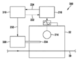
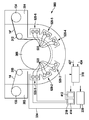
FIG. 2 illustrates a closed
As shown in FIG. 2, the cathode assembly may include a
According to some embodiments that may be combined with other embodiments disclosed herein, the
As indicated by
In accordance with exemplary embodiments, a
Thus, the voltage set
Accordingly, in accordance with some embodiments disclosed herein, the voltage of the power supply is fixed by the set point value and the output power of the
FIG. 3 illustrates a
According to other embodiments that may be combined with other embodiments disclosed herein, an AC power source may be connected to a counter electrode provided by one cathode, and the housing, by another part of the deposition apparatus, or by another electrode Lt; / RTI > For example, another electrode may be provided on the side of the substrate opposite the
According to typical embodiments, the cathodes may be magnetron sputtering cathodes. Also, planar cathodes as shown in Fig. 2 or rotatable cathodes as shown in Figs. 3 and 5 can be used for the reactive deposition process, the respective control assemblies, and the deposition apparatus as described herein.
As can be appreciated, when AC power is applied,
3, a voltage set
The gas flow rate provided by the
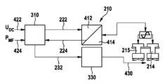
FIG. 4 shows another embodiment of a closed loop control assembly for powering
Typically, the
In accordance with the exemplary embodiments disclosed herein, a voltage set
In accordance with typical embodiments, the oxygen flow can be adjusted within certain limits and can be adjusted by a predetermined increment. Closed-loop control is implemented to provide essentially constant power, as indicated by arrows from
FIG. 6 illustrates
FIG. 5 illustrates an example of a
The
The processing modules of the
The exemplary apparatus shown in FIG. 5 includes a first deposition assembly configured to deposit a layer or layer stack on
In accordance with some embodiments that may be combined with other embodiments disclosed herein, it is contemplated that the apparatus 600 may include six compartments (not shown) such that each compartment may be operated under separate processing parameters, , Chambers or sub-chambers. As shown in FIG. 5, the apparatus comprises six rotatable MF cathodes or target assemblies 520-1 through 520-6 having Si targets, for example, sprayed
In accordance with exemplary embodiments, power supplies and gas supplies may be provided for each of the compartments of the deposition apparatus and the
In accordance with some embodiments disclosed herein, particularly for the deposition of layer stacks comprising different layers, one or several of the deposition assemblies 520-1 through 520-6 may be provided for a reactive deposition process, Loop control assembly in accordance with the embodiments disclosed herein.
For example, a three-layer, transparent layer stack having three silicon-containing dielectric films (SiO 2 or Si 3 N 4 ) can be fabricated with a closed loop control according to the embodiments disclosed herein. Thereby, a lambda-sensor or PEM can be excluded for one or more of the deposition chambers.
According to still further embodiments, the
As described above, in accordance with some embodiments that may be combined with other embodiments disclosed herein, the MF generator is a P MF -controlled or U MF control type. Thus, typically, as the voltage limit is not reached, the power control of the generator or process can be used by closed-loop control of the flow rate of the process gas. The P MF set point provided by the power supply can be set to about 10% higher than the requested process P MF - Set set point. U The DC / MF threshold set point will be changed to the process requested set point U DC / MF - Set .
The oxygen flow will change depending on the difference between the requested MF-power (PMF-Set) and the actual MF-power (PMF-Act). If the PMF-Act is smaller than the PMF-Set, the gas flow, for example oxygen flow, is increased. If the PMF-Act is larger than the PMF-Set, the gas flow, for example oxygen flow, is reduced.
The gas flow, for example, the oxygen flow, can be varied within the limits (FlowMinLimit and FlowMaxLimit) by the incremental flow per minute (deltaFlow). In addition to MF-power control by varying the gas flow rate, typically the actual voltage UDC / MF-Act should approach the set point voltage UDC / MF-Set. If the actual voltage is below the threshold limit, oxygen mode deposition is detected and counter-measures as described above can be provided.
In accordance with the embodiments disclosed herein, additional hardware, such as PEM or lambda sensors, is not required in closed loop control assemblies as disclosed herein, devices including closed loop control assemblies, and reactive layer deposition methods. In addition, a stable deposition rate, i.e. a sufficient deposition rate, can be provided in the transition mode.
The written description uses examples to include the optimum mode, to disclose the invention, and also to enable any person skilled in the art to make and use the invention. Although the invention has been described in connection with various specific embodiments, those skilled in the art will understand that the invention may be practiced with modifications within the spirit and scope of the claims. In particular, the mutually non-exclusive features of the embodiments and embodiments of the above-described embodiments or variations of the embodiments may be combined with one another.
The patentable scope of the invention is defined by the claims, and may include other examples that may occur to those skilled in the art. Such other examples are intended to be included within the scope of the claims.
While the foregoing is directed to embodiments of the invention, other and further embodiments of the invention may be devised without departing from the basic scope thereof, and the scope thereof is determined by the claims that follow.
Claims (15)
Providing power to a cathode using a power source;
Providing a voltage setpoint for the power supply;
Receiving a power value correlated with power provided to the cathode; And
And controlling the flow of the process gas in dependence on the power value to provide closed loop control.
Wherein the power provided to the cathode is MF power, especially where the oscillation frequency is between 1 kHz and 200 kHz.
Wherein the voltage setpoint is an upper limit for the power supply.
Wherein the voltage set point is configured to operate the cathode in a transition mode.
Wherein the power value is the actual power provided to the cathode, particularly as MF power.
And the received power value is stabilized by controlling the flow of the process gas.
Wherein the process gas comprises oxygen, and in particular the oxygen flow is controlled.
Receiving an actual voltage value of a voltage provided by the power source, and monitoring a deposition mode based on the actual value.
A power source coupled to the cathode to provide power to the cathode;
A gas supply configured to provide a process gas into the chamber; And
A controller coupled to the power source to provide a voltage setpoint for the power source and to receive a power value from the power source, the controller being operable to control the gas flow of the process gas in dependence upon the power value Additionally connected -
And a closed loop control assembly.
Wherein the power value is the power provided to the cathode.
Wherein the power source is an MF power source, particularly having a DC generator and an oscillator.
Wherein the power source is configured to provide power having an oscillation frequency between 1 kHz and 200 kHz.
Wherein the controller comprises program code configured for an assembly for implementing at least one of the methods according to any one of claims 1-8.
Wherein the voltage set point is an upper voltage limit line.
A chamber for depositing a layer on a substrate therein;
A cathode for generating a plasma in the chamber; And
A deposition apparatus comprising a closed loop control assembly according to any one of claims 9 to 14.
Applications Claiming Priority (1)
| Application Number | Priority Date | Filing Date | Title |
|---|---|---|---|
| PCT/EP2011/071425 WO2013079108A1 (en) | 2011-11-30 | 2011-11-30 | Closed loop control |
Related Child Applications (1)
| Application Number | Title | Priority Date | Filing Date |
|---|---|---|---|
| KR1020187035066A Division KR20180132975A (en) | 2011-11-30 | 2011-11-30 | Closed loop control |
Publications (1)
| Publication Number | Publication Date |
|---|---|
| KR20140097510A true KR20140097510A (en) | 2014-08-06 |
Family
ID=45349469
Family Applications (2)
| Application Number | Title | Priority Date | Filing Date |
|---|---|---|---|
| KR1020147017890A KR20140097510A (en) | 2011-11-30 | 2011-11-30 | Closed loop control |
| KR1020187035066A KR20180132975A (en) | 2011-11-30 | 2011-11-30 | Closed loop control |
Family Applications After (1)
| Application Number | Title | Priority Date | Filing Date |
|---|---|---|---|
| KR1020187035066A KR20180132975A (en) | 2011-11-30 | 2011-11-30 | Closed loop control |
Country Status (7)
| Country | Link |
|---|---|
| US (1) | US9758855B2 (en) |
| EP (1) | EP2785892B1 (en) |
| JP (1) | JP6305929B2 (en) |
| KR (2) | KR20140097510A (en) |
| CN (1) | CN103958723B (en) |
| TW (1) | TWI592510B (en) |
| WO (1) | WO2013079108A1 (en) |
Families Citing this family (10)
| Publication number | Priority date | Publication date | Assignee | Title |
|---|---|---|---|---|
| CN105206496B (en) | 2008-08-04 | 2019-07-05 | 北美Agc平板玻璃公司 | Plasma source and with the chemical vapor deposition of plasma enhancing come the method for depositing thin film coatings |
| WO2016034197A1 (en) * | 2014-09-01 | 2016-03-10 | Applied Materials, Inc. | Assembly and method for deposition of material on a substrate |
| KR102365939B1 (en) | 2014-12-05 | 2022-02-22 | 에이지씨 플랫 글래스 노스 아메리카, 인코퍼레이티드 | Plasma source utilizing a macro-particle reduction coating and method of using a plasma source utilizing a macro-particle reduction coating for deposition of thin film coatings and modification of surfaces |
| JP6710686B2 (en) | 2014-12-05 | 2020-06-17 | エージーシー ガラス ヨーロッパ | Hollow cathode plasma source, substrate treatment method |
| US9721765B2 (en) * | 2015-11-16 | 2017-08-01 | Agc Flat Glass North America, Inc. | Plasma device driven by multiple-phase alternating or pulsed electrical current |
| US10242846B2 (en) | 2015-12-18 | 2019-03-26 | Agc Flat Glass North America, Inc. | Hollow cathode ion source |
| US10573499B2 (en) | 2015-12-18 | 2020-02-25 | Agc Flat Glass North America, Inc. | Method of extracting and accelerating ions |
| DE102016116762B4 (en) * | 2016-09-07 | 2021-11-11 | Fraunhofer-Gesellschaft zur Förderung der angewandten Forschung e.V. | Method for depositing a layer by means of a magnetron sputtering device |
| KR102512001B1 (en) | 2017-11-09 | 2023-03-21 | 어플라이드 머티어리얼스, 인코포레이티드 | Ex-situ Solid Electrolyte Interfacial Modification Using Chalcogenides for a Lithium Metal Anode |
| US11631840B2 (en) | 2019-04-26 | 2023-04-18 | Applied Materials, Inc. | Surface protection of lithium metal anode |
Family Cites Families (10)
| Publication number | Priority date | Publication date | Assignee | Title |
|---|---|---|---|---|
| DE2821119C2 (en) | 1978-05-13 | 1983-08-25 | Leybold-Heraeus GmbH, 5000 Köln | Method and arrangement for regulating the discharge process in a cathode sputtering system |
| US4201645A (en) | 1978-06-26 | 1980-05-06 | Robert J. Ferran | Closed-loop sputtering system and method of operating same |
| DE4106513C2 (en) * | 1991-03-01 | 2002-06-13 | Unaxis Deutschland Holding | Method for regulating a reactive sputtering process and device for carrying out the method |
| US6106676A (en) * | 1998-04-16 | 2000-08-22 | The Boc Group, Inc. | Method and apparatus for reactive sputtering employing two control loops |
| US6365010B1 (en) | 1998-11-06 | 2002-04-02 | Scivac | Sputtering apparatus and process for high rate coatings |
| US6537428B1 (en) * | 1999-09-02 | 2003-03-25 | Veeco Instruments, Inc. | Stable high rate reactive sputtering |
| JP3866615B2 (en) * | 2002-05-29 | 2007-01-10 | 株式会社神戸製鋼所 | Reactive sputtering method and apparatus |
| DE102004006131B4 (en) | 2004-02-07 | 2005-12-15 | Applied Films Gmbh & Co. Kg | Strip coater with a vacuum chamber and a coating roll |
| JP2010229523A (en) * | 2009-03-27 | 2010-10-14 | Bridgestone Corp | Deposition method of conductive transparent compound thin film and conductive transparent compound thin film |
| DE102009061065A1 (en) | 2009-06-26 | 2011-09-29 | Von Ardenne Anlagentechnik Gmbh | Process for coating a substrate in a vacuum chamber with a rotating magnetron |
-
2011
- 2011-11-30 US US14/357,168 patent/US9758855B2/en not_active Expired - Fee Related
- 2011-11-30 KR KR1020147017890A patent/KR20140097510A/en active Application Filing
- 2011-11-30 EP EP11796945.1A patent/EP2785892B1/en not_active Revoked
- 2011-11-30 CN CN201180075166.4A patent/CN103958723B/en active Active
- 2011-11-30 WO PCT/EP2011/071425 patent/WO2013079108A1/en active Application Filing
- 2011-11-30 KR KR1020187035066A patent/KR20180132975A/en not_active Application Discontinuation
- 2011-11-30 JP JP2014543775A patent/JP6305929B2/en active Active
-
2012
- 2012-11-29 TW TW101144735A patent/TWI592510B/en active
Also Published As
| Publication number | Publication date |
|---|---|
| CN103958723A (en) | 2014-07-30 |
| KR20180132975A (en) | 2018-12-12 |
| TWI592510B (en) | 2017-07-21 |
| EP2785892A1 (en) | 2014-10-08 |
| JP6305929B2 (en) | 2018-04-04 |
| WO2013079108A1 (en) | 2013-06-06 |
| EP2785892B1 (en) | 2017-09-27 |
| US20150152542A1 (en) | 2015-06-04 |
| JP2015500921A (en) | 2015-01-08 |
| CN103958723B (en) | 2017-04-05 |
| TW201329279A (en) | 2013-07-16 |
| US9758855B2 (en) | 2017-09-12 |
Similar Documents
| Publication | Publication Date | Title |
|---|---|---|
| KR20140097510A (en) | Closed loop control | |
| US11680322B2 (en) | Method for forming a laminated film on a substrate | |
| EP2003225B1 (en) | Ion gun system, vapor deposition apparatus and process for producing lens | |
| TWI526564B (en) | Film forming apparatus and film forming method | |
| JP4524209B2 (en) | Deposition equipment | |
| JP6596474B2 (en) | Closed loop control | |
| US8992742B2 (en) | Method for coating a substrate in a vacuum chamber having a rotating magnetron | |
| US6783640B2 (en) | Sputtering method and sputtering apparatus | |
| EP3050073B1 (en) | Method for controlling a gas supply to a process chamber, controller for controlling a gas supply to a process chamber, and apparatus thereof | |
| US6456483B1 (en) | Electrodes for electrolytic capacitors and production process thereof | |
| WO2019154490A1 (en) | Deposition apparatus, method of coating a flexible substrate and flexible substrate having a coating | |
| KR102271227B1 (en) | Methods and apparatus for making flexible layer stacks, and flexible layer stacks | |
| KR20170048510A (en) | Assembly and method for deposition of material on a substrate | |
| TWI812642B (en) | Method and processing system for controlling a thickness of a ceramic layer on a substrate and roll-to-roll system using the same | |
| CN107916406B (en) | Method and magnetron device for bipolar magnetron sputtering | |
| JP2015074790A (en) | Plasma treatment apparatus and treatment method |
Legal Events
| Date | Code | Title | Description |
|---|---|---|---|
| AMND | Amendment | ||
| AMND | Amendment | ||
| E902 | Notification of reason for refusal | ||
| AMND | Amendment | ||
| E601 | Decision to refuse application | ||
| AMND | Amendment | ||
| A107 | Divisional application of patent | ||
| J201 | Request for trial against refusal decision | ||
| J301 | Trial decision |
Free format text: TRIAL NUMBER: 2018101004909; TRIAL DECISION FOR APPEAL AGAINST DECISION TO DECLINE REFUSAL REQUESTED 20181203 Effective date: 20191119 |