KR20140094914A - Dispaly apparatus having backlight assembly - Google Patents
Dispaly apparatus having backlight assembly Download PDFInfo
- Publication number
- KR20140094914A KR20140094914A KR1020130007569A KR20130007569A KR20140094914A KR 20140094914 A KR20140094914 A KR 20140094914A KR 1020130007569 A KR1020130007569 A KR 1020130007569A KR 20130007569 A KR20130007569 A KR 20130007569A KR 20140094914 A KR20140094914 A KR 20140094914A
- Authority
- KR
- South Korea
- Prior art keywords
- light
- light emitting
- guide plate
- light guide
- emitting diodes
- Prior art date
Links
Images


Classifications
-
- A—HUMAN NECESSITIES
- A41—WEARING APPAREL
- A41B—SHIRTS; UNDERWEAR; BABY LINEN; HANDKERCHIEFS
- A41B9/00—Undergarments
- A41B9/02—Drawers or underpants for men, with or without inserted crotch or seat parts
- A41B9/023—Drawers or underpants for men, with or without inserted crotch or seat parts with separate spaces for genitals
-
- G—PHYSICS
- G02—OPTICS
- G02B—OPTICAL ELEMENTS, SYSTEMS OR APPARATUS
- G02B6/00—Light guides; Structural details of arrangements comprising light guides and other optical elements, e.g. couplings
- G02B6/0001—Light guides; Structural details of arrangements comprising light guides and other optical elements, e.g. couplings specially adapted for lighting devices or systems
- G02B6/0011—Light guides; Structural details of arrangements comprising light guides and other optical elements, e.g. couplings specially adapted for lighting devices or systems the light guides being planar or of plate-like form
- G02B6/0013—Means for improving the coupling-in of light from the light source into the light guide
- G02B6/0023—Means for improving the coupling-in of light from the light source into the light guide provided by one optical element, or plurality thereof, placed between the light guide and the light source, or around the light source
- G02B6/0031—Reflecting element, sheet or layer
-
- G—PHYSICS
- G02—OPTICS
- G02B—OPTICAL ELEMENTS, SYSTEMS OR APPARATUS
- G02B6/00—Light guides; Structural details of arrangements comprising light guides and other optical elements, e.g. couplings
- G02B6/0001—Light guides; Structural details of arrangements comprising light guides and other optical elements, e.g. couplings specially adapted for lighting devices or systems
- G02B6/0011—Light guides; Structural details of arrangements comprising light guides and other optical elements, e.g. couplings specially adapted for lighting devices or systems the light guides being planar or of plate-like form
- G02B6/0013—Means for improving the coupling-in of light from the light source into the light guide
- G02B6/0015—Means for improving the coupling-in of light from the light source into the light guide provided on the surface of the light guide or in the bulk of it
- G02B6/0018—Redirecting means on the surface of the light guide
-
- G—PHYSICS
- G02—OPTICS
- G02B—OPTICAL ELEMENTS, SYSTEMS OR APPARATUS
- G02B6/00—Light guides; Structural details of arrangements comprising light guides and other optical elements, e.g. couplings
- G02B6/0001—Light guides; Structural details of arrangements comprising light guides and other optical elements, e.g. couplings specially adapted for lighting devices or systems
- G02B6/0011—Light guides; Structural details of arrangements comprising light guides and other optical elements, e.g. couplings specially adapted for lighting devices or systems the light guides being planar or of plate-like form
- G02B6/0066—Light guides; Structural details of arrangements comprising light guides and other optical elements, e.g. couplings specially adapted for lighting devices or systems the light guides being planar or of plate-like form characterised by the light source being coupled to the light guide
- G02B6/0068—Arrangements of plural sources, e.g. multi-colour light sources
-
- A—HUMAN NECESSITIES
- A41—WEARING APPAREL
- A41B—SHIRTS; UNDERWEAR; BABY LINEN; HANDKERCHIEFS
- A41B2400/00—Functions or special features of shirts, underwear, baby linen or handkerchiefs not provided for in other groups of this subclass
- A41B2400/20—Air permeability; Ventilation
-
- G—PHYSICS
- G02—OPTICS
- G02B—OPTICAL ELEMENTS, SYSTEMS OR APPARATUS
- G02B6/00—Light guides; Structural details of arrangements comprising light guides and other optical elements, e.g. couplings
- G02B6/0001—Light guides; Structural details of arrangements comprising light guides and other optical elements, e.g. couplings specially adapted for lighting devices or systems
- G02B6/0011—Light guides; Structural details of arrangements comprising light guides and other optical elements, e.g. couplings specially adapted for lighting devices or systems the light guides being planar or of plate-like form
- G02B6/0081—Mechanical or electrical aspects of the light guide and light source in the lighting device peculiar to the adaptation to planar light guides, e.g. concerning packaging
- G02B6/0086—Positioning aspects
- G02B6/0091—Positioning aspects of the light source relative to the light guide
Landscapes
- Physics & Mathematics (AREA)
- General Physics & Mathematics (AREA)
- Optics & Photonics (AREA)
- Engineering & Computer Science (AREA)
- Health & Medical Sciences (AREA)
- Reproductive Health (AREA)
- Textile Engineering (AREA)
- Planar Illumination Modules (AREA)
- Liquid Crystal (AREA)
- Devices For Indicating Variable Information By Combining Individual Elements (AREA)
- Microelectronics & Electronic Packaging (AREA)
Abstract
Description
본 발명은 백라이트 어셈블리를 갖는 표시장치에 관한 것으로, 보다 상세하게는, 백라이트 어셈블리 및 상기 백라이트 어셈블리로부터 출력된 광을 이용하여 영상을 표시하는 표시패널을 포함하는 표시장치에 관한 것이다. BACKGROUND OF THE
액정표시장치와 같이 자체적으로 광을 발생시키지 않는 표시패널을 포함하는 표시장치는 그 구성 요소로 광을 출력하는 백라이트 어셈블리를 포함한다. 상기 백라이트 어셈블리는 외부로부터 전원을 제공받아 광을 발생시키는 발광 유닛을 포함하고, 일반적으로 상기 발광 유닛의 광원으로 냉음극 형광램프(Cold Cathode Fluorescent Lamp, CCFL) 또는 LED 패키지가 적용될 수 있다. A display device including a display panel such as a liquid crystal display device that does not generate light itself includes a backlight assembly that outputs light to the components. The backlight assembly includes a light emitting unit that receives power from the outside to generate light. Generally, a cold cathode fluorescent lamp (CCFL) or an LED package may be used as a light source of the light emitting unit.
상기 백라이트 어셈블리가 상기 LED 패키지를 포함하는 경우에, 상기 LED 패키지가 인쇄회로기판 위에 다수로 실장되어 상기 다수의 LED 패키지들은 상기 인쇄회로기판으로부터 전원을 제공받아 발광한다. In a case where the backlight assembly includes the LED package, the LED package is mounted on the PCB, and the plurality of LED packages are powered by the PCB.
한편, 상기 백라이트 어셈블리의 제조 비용을 감소시키기 위하여 상기 인쇄회로기판 위에 실장되는 상기 다수의 LED 패키지들의 개수를 감소시키고, 상기 인쇄회로기판의 길이를 감소시키는 방안이 제안되고 있으나, 이 경우에, 상기 백라이트 어셈블리로부터 출력되는 광의 휘도를 균일하게 하기 위하여 상기 백라이트 어셈블리의 구조가 변경될 수 있다. In order to reduce the manufacturing cost of the backlight assembly, there has been proposed a method of reducing the number of the plurality of LED packages mounted on the printed circuit board and reducing the length of the printed circuit board. In this case, The structure of the backlight assembly may be changed in order to make the brightness of light output from the backlight assembly uniform.
본 발명의 목적은 제조 비용이 감소되고, 광을 균일하게 출력하는 백라이트 어셈블리를 포함하여 표시 품질이 향상된 표시 장치를 제공하는 데 있다. An object of the present invention is to provide a display device having improved display quality including a backlight assembly that reduces manufacturing cost and outputs light uniformly.
상술한 본 발명의 목적을 달성하기 위해서, 본 발명에 따른 표시 장치는 광을 출력하는 백라이트 어셈블리 및 상기 광을 제공받아 영상을 표시하는 표시패널을 포함한다. According to an aspect of the present invention, there is provided a display device including a backlight assembly for outputting light and a display panel for receiving the light and displaying an image.
상기 백라이트 어셈블리는 발광 유닛, 도광판, 및 반사부재를 포함한다. 상기 발광 유닛은 상기 광을 발생한다. 상기 도광판은 상기 발광 유닛으로부터 제공된 광을 상기 표시패널 측으로 가이드하고, 상기 도광판은 측면으로부터 돌출된 돌출부를 갖는다. 또한, 상기 반사부재는 상기 돌출부의 표면 위에 배치되어 상기 발광 유닛으로부터 상기 돌출부 측으로 제공된 광을 상기 도광판의 코너부 및 상기 코너부의 주변으로 반사시킨다. The backlight assembly includes a light emitting unit, a light guide plate, and a reflective member. The light emitting unit generates the light. The light guide plate guides the light provided from the light emitting unit to the display panel side, and the light guide plate has a protrusion protruding from the side surface. Further, the reflective member is disposed on the surface of the protruding portion, and reflects the light provided from the light emitting unit toward the protruding portion toward the corner portion of the light guide plate and the periphery of the corner portion.
상술한 본 발명의 목적을 달성하기 위해서, 본 발명에 따른 다른 표시장치는 광을 출력하는 백라이트 어셈블리 및 상기 광을 제공받아 영상을 표시하는 표시패널을 포함한다. According to another aspect of the present invention, there is provided a display apparatus including a backlight assembly for outputting light and a display panel for receiving the light and displaying an image.
상기 백라이트 어셈블리는 발광 유닛 및 상기 발광 유닛으로부터 제공된 광을 상기 표시패널 측으로 가이드하는 도광판을 포함하고, 상기 발광 유닛은 인쇄회로기판 및 다수의 발광 다이오드들을 포함한다. The backlight assembly includes a light emitting unit and a light guide plate guiding the light provided from the light emitting unit to the display panel side, wherein the light emitting unit includes a printed circuit board and a plurality of light emitting diodes.
상기 인쇄회로기판은 상기 도광판과 수평으로 배치되어 평면상에서 상기 도광판의 제1 코너부와 중첩된다. 또한, 상기 다수의 발광 다이오드들은 상기 인쇄회로기판 위에 배치되고, 상기 제1 코너부를 정의하는 두 측면들을 통해 상기 도광판 측으로 광을 제공한다. The printed circuit board is disposed horizontally with the light guide plate and overlapped with the first corner of the light guide plate on a plane. The plurality of light emitting diodes are disposed on the printed circuit board and provide light to the light guide plate side through two sides defining the first corner.
본 발명의 일 실시예에 따르면, 도광판에 입사된 광 중 도광판의 돌출부가 갖는 경사면 측에 제공된 광은 반사부재에 의해 도광판의 코너부 측으로 반사된다. 따라서, 발광 유닛의 배치에 따라 제공되는 광량이 감소될 수 있는 상기 도광판의 코너부에 제공되는 광량이 보충될 수 있으므로, 상기 도광판의 전체 영역에 걸쳐 균일하게 광량이 제공될 수 있다. 또한, 상술한 구조를 갖는 도광판을 갖는 백라이트 어셈블리로부터 출력되는 광을 이용하여 영상을 표시하는 표시장치의 표시 품질이 향상될 수 있다. According to an embodiment of the present invention, the light provided on the side of the inclined surface of the protrusion of the light guide plate among the light incident on the light guide plate is reflected toward the corner portion side of the light guide plate by the reflection member. Therefore, the amount of light provided to the corner portion of the light guide plate, which can be reduced according to the arrangement of the light emitting units, can be supplemented, so that the light amount can be uniformly distributed over the entire area of the light guide plate. Further, display quality of a display device for displaying an image using the light output from the backlight assembly having the light guide plate having the above-described structure can be improved.
또한, 상술한 바와 같이, 상기 반사부재를 이용하여 상기 도광판의 상기 코너부에 제공되는 광량이 보충될 수 있으므로, 상기 발광 유닛은 상기 도광판의 상기 코너부까지 배치되지 않아도 된다. 따라서, 상기 백라이트 어셈블리에서 상기 발광 유닛이 갖는 발광 다이오드들의 개수가 감소되고, 상기 발광 다이오드들이 실장되는 인쇄회로기판의 길이가 감소될 수 있으므로, 상기 백라이트 어셈블리 및 이를 갖는 표시 장치의 제조 비용이 감소될 수 있다. Further, as described above, since the light amount provided to the corner portion of the light guide plate can be supplemented by using the reflective member, the light emitting unit may not be disposed to the corner portion of the light guide plate. Accordingly, since the number of light emitting diodes included in the light emitting unit in the backlight assembly is reduced and the length of the printed circuit board on which the light emitting diodes are mounted can be reduced, the manufacturing cost of the backlight assembly and the display device having the reduced number of LEDs is reduced .
또한, 본 발명의 다른 실시예에 따르면, 발광 유닛의 발광 다이오드들이 배치되는 간격이 증가하여 서로 인접한 두 개의 발광 다이오드들 사이에 대응하여 상기 도광판에 입력되는 광량이 적더라도, 상기 반사부재에서 반사되어 상기 도광판의 상기 코너부 측으로 진행하는 광을 이용하여 상기 도광판에 광량이 적게 입사되는 부분에 광량이 보충될 수 있다. In addition, according to another embodiment of the present invention, even if the interval at which the light emitting diodes of the light emitting unit are disposed increases and the amount of light input to the light guide plate corresponding to the two adjacent light emitting diodes is small, The amount of light can be supplemented to a portion of the light guide plate where light is incident at a small amount using light traveling toward the corner portion of the light guide plate.
또한, 본 발명의 또 다른 실시예에 따르면, 평면상에서 상기 도광판의 코너부와 중첩되도록 인쇄회로기판을 도광판과 수평으로 배치하고, 상기 도광판의 제1 코너부를 정의하는 두 측면들에 마주하도록 상기 인쇄회로기판 위에 다수의 발광 다이오드들을 배치할 수 있다. 따라서, 상기 다수의 발광 다이오드들을 이용하여 상기 제1 코너부와 대향하는 제2 코너부 측으로 광을 용이하게 제공할 수 있다. 따라서, 상기 인쇄회로기판 및 상기 다수의 발광 다이오드들은 상기 제1 코너부까지 배치되지 않아도 되므로, 백라이트 어셈블리 및 이를 갖는 표시 장치의 제조 비용이 감소될 수 있다. According to another embodiment of the present invention, a printed circuit board is disposed horizontally with the light guide plate so as to overlap with a corner of the light guide plate on a plane, and the printed circuit board is disposed so as to face the two sides defining the first corner of the light guide plate. A plurality of light emitting diodes can be arranged on a circuit board. Therefore, light can be easily provided to the second corner portion facing the first corner portion using the plurality of light emitting diodes. Therefore, since the printed circuit board and the plurality of light emitting diodes are not disposed to the first corner, the manufacturing cost of the backlight assembly and the display device having the backlight assembly can be reduced.
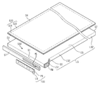
도 1은 본 발명의 일 실시예에 따른 표시 장치의 분해 사시도이다.
도 2a는 도 1의 I-I'을 따라 절취된 면을 나타내는 단면도이다.
도 2b는 도 1에 도시된 발광 유닛, 도광판, 반사부재 및 표시패널의 결합 상태를 나타내는 분해 사시도이다.
도 3은 도 2b에 도시된 도광판 측으로 입사된 광의 분포를 나타내는 평면도이다.
도 4는 본 발명의 다른 실시예에 따른 도광판 및 발광 유닛을 도시한 평면도이다.
도 5는 본 발명의 또 다른 실시예에 따른 도광판 및 발광 유닛을 도시한 평면도이다.
도 6a는 본 발명의 또 다른 실시예에 따른 표시장치의 단면도이다.
도 6b는 도 6a에 도시된 발광 유닛, 도광판, 반사부재 및 표시패널의 결합 상태를 나타내는 분해 사시도이다.
도 7a는 본 발명의 또 다른 실시예에 따른 표시장치의 단면도이다.
도 7b는 도 7a에 도시된 발광 유닛, 도광판, 반사부재, 표시패널 및 수납용기의 결합 상태를 나타내는 분해 사시도이다.
도 8a는 본 발명의 또 다른 실시예에 따른 발광 유닛, 도광판, 및 표시패널의 결합 상태를 나타내는 분해 사시도이다.
도 8b는 도 8a에 도시된 도광판 측으로 입사된 광의 분포를 나타내는 평면도이다. 1 is an exploded perspective view of a display device according to an embodiment of the present invention.
FIG. 2A is a cross-sectional view taken along the line I-I 'of FIG. 1; FIG.
FIG. 2B is an exploded perspective view showing a state of engagement between the light emitting unit, the light guide plate, the reflecting member, and the display panel shown in FIG.
3 is a plan view showing the distribution of light incident on the light guide plate side shown in FIG. 2B.
4 is a plan view showing a light guide plate and a light emitting unit according to another embodiment of the present invention.
5 is a plan view illustrating a light guide plate and a light emitting unit according to another embodiment of the present invention.
6A is a cross-sectional view of a display device according to another embodiment of the present invention.
FIG. 6B is an exploded perspective view showing the state of engagement between the light emitting unit, the light guide plate, the reflecting member, and the display panel shown in FIG. 6A.
7A is a cross-sectional view of a display device according to another embodiment of the present invention.
FIG. 7B is an exploded perspective view showing the combined state of the light emitting unit, the light guide plate, the reflecting member, the display panel, and the storage container shown in FIG. 7A.
FIG. 8A is an exploded perspective view illustrating a coupled state of a light emitting unit, a light guide plate, and a display panel according to another embodiment of the present invention. FIG.
FIG. 8B is a plan view showing the distribution of light incident on the light guide plate side shown in FIG. 8A. FIG.
이하 첨부한 도면들을 참조하여 본 발명의 실시예들을 상세히 살펴보기로 한다. 상기한 본 발명의 목적, 특징 및 효과는 도면과 관련된 실시예들을 통해서 용이하게 이해될 수 있을 것이다. 다만, 본 발명은 여기서 설명되는 실시예들에 한정되지 않고, 다양한 형태로 응용되어 변형될 수도 있다. 오히려 후술될 본 발명의 실시예들은 본 발명에 의해 개시된 기술 사상을 보다 명확히 하고, 나아가 본 발명이 속하는 분야에서 평균적인 지식을 가진 당업자에게 본 발명의 기술 사상이 충분히 전달될 수 있도록 제공되는 것이다. 따라서, 본 발명의 범위가 후술될 실시예들에 의해 한정되는 것으로 해석되어서는 안 될 것이다. 한편, 하기 실시예와 도면 상에 동일한 참조 번호들은 동일한 구성 요소를 나타낸다. Hereinafter, embodiments of the present invention will be described in detail with reference to the accompanying drawings. The above and other objects, features and advantages of the present invention will become more apparent from the following detailed description of the present invention when taken in conjunction with the accompanying drawings. However, the present invention is not limited to the embodiments described herein, but may be modified in various forms. Rather, the embodiments of the present invention will be described in greater detail with reference to the accompanying drawings, in which: FIG. Accordingly, the scope of the present invention should not be construed as being limited by the embodiments described below. In the following embodiments and the drawings, the same reference numerals denote the same elements.
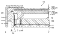
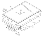
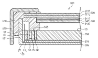
도 1은 본 발명의 일 실시예에 따른 표시 장치의 분해 사시도이고, 도 2a는 도 1의 I-I'을 따라 절취된 면을 나타내는 단면도이고, 도 2b는 도 1에 도시된 발광 유닛, 도광판, 반사부재 및 표시패널의 결합 상태를 나타내는 도면이다. 1 is an exploded perspective view of a display device according to an embodiment of the present invention. FIG. 2A is a cross-sectional view taken along line I-I 'of FIG. 1, , A reflective member, and a display panel.
도 1, 도 2a 및 도 2b를 참조하면, 표시 장치(600)는 백라이트 어셈블리(500) 및 표시패널(520)을 포함한다. 상기 백라이트 어셈블리(500)는 광을 출력하고, 상기 표시패널(520)은 상기 백라이트 어셈블리(500)로부터 상기 광을 제공받아 표시 영역(DA)에서 영상을 표시한다. Referring to FIGS. 1, 2A, and 2B, a
본 발명의 실시예에서는, 상기 표시 패널(520)은 액정표시패널일 수 있고, 이 경우에, 상기 표시 패널(520)은 다수의 화소 전극들을 갖는 제1 기판(521), 상기 다수의 화소 전극들과 대향하는 공통 전극을 갖는 제2 기판(522), 및 상기 제1 기판(521)과 상기 제2 기판(522) 사이에 개재된 액정층(미도시)을 포함할 수 있다. 하지만, 본 발명이 상기 표시 패널(520)의 종류에 한정되는 것은 아니다. 예를 들어, 상기 표시패널(520)은, 전기습윤 표시패널 (Electrowetting display panel) 및 나노 크리스탈 표시패널(nano-crystal display panel)과 같이, 자체적으로 광을 발생하지 않는 다른 종류의 표시패널일 수도 있다.In an embodiment of the present invention, the
상기 백라이트 어셈블리(500)는 발광 유닛(100), 수납용기(580), 반사판(570), 도광판(550), 몰드 프레임(530), 다수의 시트들(540), 및 커버부재(510)를 포함한다. The
상기 발광 유닛(100)은 광을 발생한다. 본 발명의 실시예에서는, 상기 발광 유닛(100)은 인쇄회로기판(PB) 및 상기 인쇄회로기판(PB) 위에 실장되어 상기 광을 발생하는 다수의 발광다이오드들(LG)을 포함할 수 있다. 상기 인쇄회로기판(PB)은 상기 도광판(550)의 제1 면(S1)을 따라 신장될 수 있고, 이에 따라, 상기 다수의 발광다이오드들(LG)로부터 발생된 광은 상기 제1 면(S1)을 통해 상기 도광판(550) 측으로 입사될 수 있다. The
이 실시예에서는, 상기 인쇄회로기판(PB)은 상기 도광판(550)에 대해 수직으로 배치될 수 있다. 하지만, 이 실시예와 달리, 도 8a에 도시된 바와 같이, 상기 인쇄회로기판(PB)은 상기 도광판(550)에 대해 수평으로 배치될 수도 있다. In this embodiment, the printed circuit board PB may be disposed perpendicular to the
상기 수납용기(580)는 바닥부(585) 및 상기 바닥부(585)로부터 연장된 다수의 측벽들(581)을 구비하여, 상기 백라이트 어셈블리(500)의 구성 요소들을 수납한다. 상술한 바와 같이, 상기 인쇄회로기판(PB)이 상기 도광판(550)의 상기 제1 면(S1)과 인접하도록 배치되는 경우에, 상기 발광 유닛(100)은 상기 다수의 측벽들(581) 중 상기 제1 면(S1)과 대향하는 측벽 및 상기 제1 면(S1) 사이에 배치될 수 있다. The
상기 도광판(550)은 상기 발광 유닛(100)으로부터 발생된 광을 제공받아 상기 광을 상기 표시패널(520) 측으로 가이드한다. 보다 상세하게는, 상기 발광 유닛(100)으로부터 발생된 광은 상기 제1 면(S1)을 통해 상기 도광판(550)의 내부로 입사되고, 상기 도광판(550)의 내부로 입사된 광은 출사면(ES)을 통해 상기 도광판(550)로부터 출사된다. 이 실시예에서는, 상기 도광판(550)은 돌출부(555)를 포함할 수 있고, 상기 돌출부(555)는 상기 도광판(550)의 일 측면으로부터 돌출될 수 있다. The
상기 도광판(550)은, 상기 제1 면(S1) 및 상기 출사면(ES) 외에, 상기 제1 면과 대향하는 제2 면(S2), 제3 면(S3) 및 상기 제1 면(S1)과 경사진 경사면(SS)을 갖는 연결면들(LS)을 포함할 수 있다. 이 실시예에서는, 상기 제1 내지 제3 면들(S1, S2, S3) 및 상기 연결면들(LS)은 상기 도광판(550)의 측면들 일 수 있고, 이 경우에, 상기 경사면(SS)은 상기 돌출부(555)가 갖는 표면들 중 어느 하나일 수 있다. 상기 연결 면들(LS)은 상기 제1 면(S1) 및 상기 제2 면(S2) 사이에 순차적으로 배열되어 상기 제1 면(S1)을 상기 제2 면(S2)에 연결하고, 상기 제3 면(S3)은 상기 연결면들(LS)과 대향한다. The
본 발명의 실시예에서는, 상기 연결면들(LS)은 제1 연결면(LS1), 상기 경사면(SS), 및 제2 연결면(LS2)을 포함할 수 있고, 상기 제1 연결면(LS1), 상기 경사면(SS), 및 상기 제2 연결면(LS2)은 상기 제1 면(S1) 및 상기 제2 면(S2) 사이에 순차적으로 배열된다. 즉, 상기 연결 면들(LS) 중 상기 제1 연결면(LS1)은 상기 제1 면(S1)과 연결되고, 상기 제2 연결면(LS2)은 상기 제2 면(S2)과 연결되고, 상기 경사면(SS)은 상기 제1 연결면(LS1)을 상기 제2 연결면(LS2)에 연결한다. In the embodiment of the present invention, the connection surfaces LS may include a first connection surface LS1, a slope SS, and a second connection surface LS2, and the first connection surface LS1 , The inclined surface SS and the second connection surface LS2 are sequentially arranged between the first surface S1 and the second surface S2. That is, the first connection surface LS1 of the connection surfaces LS is connected to the first surface S1, the second connection surface LS2 is connected to the second surface S2, The inclined surface SS connects the first connection surface LS1 to the second connection surface LS2.
본 발명의 실시예에서는, 평면상에서 상기 제1 면(S1) 및 상기 제2 면(S2) 각각은 제1 방향(D1)과 나란하고, 평면상에서 상기 제1 및 제2 연결면들(LS1, LS2) 각각은 상기 제1 방향(D1)과 실질적으로 수직하는 제2 방향(D2)과 나란하다. 또한, 평면상에서 상기 경사면(SS)은 상기 제1 및 제2 방향들(D1, D2)과 상이한 제3 방향(D3)과 나란하고, 평면상에서 상기 돌출부(555) 및 상기 돌출부(55)가 갖는 상기 경사면(SS)은 상기 표시영역(DA)과 이격된다. 또한, 평면상에서 상기 제1 면(S1)은 상기 경사면(SS)과 예각을 형성하고, 상기 예각은 상기 제1 면(S1)으로부터 상기 경사면(SS)까지 시계 방향으로 회전하여 정의될 수 있다. In the embodiment of the present invention, each of the first surface S1 and the second surface S2 on the plane is parallel to the first direction D1, and the first and second connecting surfaces LS1, LS2 are parallel to a second direction D2 substantially perpendicular to the first direction D1. The inclined plane SS is parallel to the third direction D3 which is different from the first and second directions D1 and D2 on the plane and the
또한, 본 발명의 실시예에서는, 상기 다수의 발광다이오드들(LG)은 상기 제1 면(S1)을 따라 배열되고, 평면상에서 상기 다수의 발광다이오드들(LG) 중 처음에 배열된 발광다이오드 및 마지막에 배열된 발광다이오드 간의 거리를 제1 이격거리(LT2)로 정의하고, 평면상에서 상기 제1 면(S1)의 길이를 제1 길이(LT1)로 정의하면, 상기 제1 이격거리(LT2)는 상기 제1 길이(LT1)보다 작다. In addition, in the embodiment of the present invention, the plurality of light emitting diodes LG are arranged along the first surface S1, and the light emitting diodes are arranged on the first plane among the plurality of light emitting diodes LG on a plane, The distance between the light emitting diodes arranged last is defined as a first separation distance LT2 and the length of the first surface S1 on the plane is defined as a first length LT1, Is smaller than the first length LT1.
또한, 상기 인쇄회로기판(PB)은 대략적으로 상기 제1 이격거리(LT2)에 대응하는 길이를 가질 수 있으므로, 상기 인쇄회로기판(PB)의 길이는 상기 제1 길이(LT1)보다 작다. 따라서, 상기 인쇄회로기판(PB)이 고가의 메탈코어 인쇄회로기판(metal core printed circuit board, MCPCB)인 경우에, 상기 인쇄회로기판(PB)이 상기 제1 길이(LT1)에 상응하는 길이를 가질 필요가 없으므로 상기 인쇄회로기판(PB)의 제조 단가가 감소될 수 있고, 상기 인쇄회로기판(PB) 위에 배치되는 상기 발광다이오드들(LG)의 개수가 감소될 수 있다. Since the printed circuit board PB may have a length corresponding to the first distance LT2, the length of the printed circuit board PB is smaller than the first length LT1. Therefore, when the printed circuit board PB is an expensive metal core printed circuit board (MCPCB), the printed circuit board PB has a length corresponding to the first length LT1 The manufacturing cost of the printed circuit board PB can be reduced and the number of the light emitting diodes LG disposed on the printed circuit board PB can be reduced.
상기 반사부재(RM)는 상기 돌출부(555)의 표면 위에 배치되고, 보다 상세하게는, 상기 반사부재(RM)는 상기 경사면(SS) 위에 배치될 수 있다. 따라서, 상기 발광 유닛(100)으로부터 발생되어 상기 제1 면(S1) 및 상기 경사면(SS)을 순차적으로 투과한 광은 상기 반사부재(RM)에서 반사되어 상기 도광판(550)의 코너부 및 상기 코너부의 주변으로 제공된다. 따라서, 상기 경사면(SS) 위에 상기 반사부재(RM)를 배치함에 따라 상기 도광판(550)의 상기 코너부 및 상기 코너부의 주변에 제공되는 광량과 상기 도광판(550)의 나머지 부분에 제공되는 광량의 차이를 감소시킬 수 있다. 이에 대해서는 도 3을 참조하여 보다 상세히 설명된다. The reflective member RM is disposed on the surface of the
본 발명의 실시예에서는, 상기 반사부재(RM)는 상기 제1 면(S1) 및 상기 경사면(SS)을 연결하는 상기 제1 연결면(LS1) 위에 더 배치될 수도 있다.In an embodiment of the present invention, the reflective member RM may be further disposed on the first connecting surface LS1 connecting the first surface S1 and the inclined surface SS.
또한, 본 발명의 실시예에서는, 상기 반사부재(RM)는 반사 테이프일 수 있다. 상기 반사 테이프는 그 표면이 거울과 같은 기능을 가질 수 있도록, 상기 표면은 은(Ag) 및 알루미늄과 같은 반사 물질로 코팅되거나, 상기 표면은 백색의 폴리에틸렌 테레프탈레이트(polyethylene terephthalate, PET), 및 폴리 카보네이트(poly carbonate, PC)와 같은 광을 반사시키는 물질로 코팅될 수 있다. Further, in the embodiment of the present invention, the reflective member RM may be a reflective tape. The surface of the reflective tape is coated with a reflective material such as silver (Ag) and aluminum, or the surface is coated with white polyethylene terephthalate (PET) and poly And may be coated with a material that reflects light, such as polycarbonate (PC).
또한, 본 발명의 다른 실시예에서는, 상기 반사부재(RM)는 상기 경사면(SS) 위에 배치된 반사층일 수도 있다. 이 경우에, 상기 반사층은 은 및 알루미늄과 같이 광반사도가 우수한 물질이 상기 경사면(SS) 위에 증착되어 형성되거나, 상기 경사면(SS) 위에 백색의 아크릴 계열의 물질이 도포되어 형성될 수도 있다. Further, in another embodiment of the present invention, the reflection member RM may be a reflection layer disposed on the inclined surface SS. In this case, the reflective layer may be formed by depositing a material having excellent light reflectivity such as silver and aluminum on the inclined surface SS, or may be formed by applying a white acrylic material on the inclined surface SS.
상기 반사판(570)은 폴리에틸렌 테레프탈레이트(polyethylene terephthalate, PET) 및 알루미늄과 같은 광을 반사하는 물질을 포함하여 상기 수납용기(580)의 바닥부(585) 및 상기 도광판(550) 사이에 배치된다. 따라서, 상기 발광 유닛(100)으로부터 발생되어 상기 도광판(550) 측으로 입사되지 못한 광은 상기 반사판(570)에 의해 반사된 후, 상기 도광판(550)에 입사될 수 있다. The
상기 몰드 프레임(530)은 상기 수납 용기(580)와 결합되어 상기 도광판(550)의 가장자리를 상기 수납 용기(580)의 상기 바닥부(585)에 지지한다. 상기 몰드 프레임(530)의 일부분은 상기 바닥부(585)와 나란한 방향으로 연장되어 상기 다수의 시트들(540) 및 상기 표시패널(520)이 상기 몰드 프레임(530) 위에 안착될 수 있다. The
상기 다수의 시트들(540)은 상기 표시 패널(520) 및 상기 도광판(550) 사이에 배치된다. 상기 다수의 시트들(540)은 상기 도광판(550)으로부터 출사되어 상기 표시 패널(520) 측으로 입사되는 광의 경로를 조절하는 광학 시트들을 포함할 수 있다. 본 발명의 실시예에서는, 상기 다수의 시트들(540)은 각각이 상기 도광판(550)으로부터 출사된 광을 확산시키는 상부 확산시트(541)와 하부 확산시트(543), 및 상기 도광판(550)으로부터 출사된 광을 집광하는 프리즘 시트(542)를 포함할 수 있다.The plurality of
상기 커버 부재(510)는 상기 표시 패널(520)의 표시 영역(DA)이 노출되도록 그 일부가 개구되고, 상기 표시패널(520)의 테두리를 커버하여 상기 수납 용기(580)와 결합된다. 상기 커버 부재(510)가 상기 수납 용기(580)에 체결됨에 따라, 상기 수납 용기(580)가 갖는 수납 공간 내에 상기 백라이트 어셈블리(500)의 구성 요소들이 안정적으로 수납될 수 있다.The
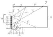
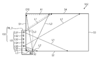
도 3은 도 2b에 도시된 도광판 측으로 입사된 광의 분포를 나타내는 평면도이다. 3 is a plan view showing the distribution of light incident on the light guide plate side shown in FIG. 2B.
도 3을 참조하면, 발광 유닛(100)은 인쇄회로기판(PB) 및 상기 인쇄회로기판(PB) 위에 실장된 다수의 발광다이오드들(LG)을 포함한다. 상기 다수의 발광다이오드들(LG)은 도광판(550)의 제1 면(S1)을 따라 배열되어, 상기 다수의 발광다이오드들(LG)로부터 발생된 광은 상기 제1 면(S1)을 통해 상기 도광판(550) 측으로 입사된다. Referring to FIG. 3, the
이 실시예에서, 상기 다수의 발광다이오드들(LG)의 개수를 6개로 가정하고, 상기 6개의 발광다이오드들(LG) 중 처음에 배열된 발광 다이오드부터 마지막에 배열된 발광다이오드들을 순차적으로 제1 내지 제6 발광다이오드들(LG1, LG2, LG3, LG4, LG5, LG6)로 정의한다. In this embodiment, assuming that the number of the plurality of light emitting diodes LG is six, the light emitting diodes arranged last from the light emitting diodes arranged first among the six light emitting diodes LG are sequentially To sixth LEDs LG1, LG2, LG3, LG4, LG5, and LG6.
이 실시예에서, 상기 제1 내지 제6 발광다이오드들(LG1, LG2, LG3, LG4, LG5, LG6) 각각으로부터 출사된 광이 방사되는 각도는 서로 동일하고, 상기 각도는 평면상에서 약 100도 내지 약 150도 일 수 있다. 예를 들어, 상기 제1 발광다이오드(LG1)로부터 발생되는 제1 광(L1)이 방사되는 제1 방사 각도(G1) 및 상기 제5 발광다이오드(LG5)로부터 발생되는 제2 광(L2)이 방사되는 제2 방사 각도(G2) 각각의 크기는 약 100도 내지 약 150도, 보다 상세하게는, 약 120도일 수 있다. In this embodiment, the angles at which the light emitted from each of the first to sixth light emitting diodes LG1, LG2, LG3, LG4, LG5, and LG6 are emitted are the same, 150 < / RTI > For example, the first radiation angle G1 at which the first light L1 emitted from the first light emitting diode LG1 is emitted and the second light L2 emitted from the fifth light emitting diode LG5 The size of each of the emitted second radiation angles G2 may be from about 100 degrees to about 150 degrees, more particularly about 120 degrees.
따라서, 상기 제1 및 제5 발광다이오들(LG1, LG5) 사이에 위치한 상기 제2 내지 제4 발광다이오드들(LG2, LG3, LG4)로부터 발생되는 광이 상기 도광판(550) 내에서 방사되는 범위는 상기 제1 및 제5 발광다이오드들(LG1, LG5)로부터 발생되는 광이 상기 도광판(550) 내에서 방사되는 범위 사이에 위치할 수 있다. Therefore, the light emitted from the second to fourth light emitting diodes LG2, LG3, and LG4 positioned between the first and fifth light emitting diodes LG1 and LG5 is emitted within the
또한, 상기 발광다이오드들(LG) 중 상기 도광판(550)의 돌출부(555)에 가장 인접한 상기 제6 발광다이오드(LG6)는 상기 돌출부(555)를 사이에 두고 상기 반사부재(RM)와 마주한다. 따라서, 상기 제6 발광다이오드(LG6)로부터 발생된 제3 광(L3)은 상기 제1 면(S1) 및 상기 경사면(SS)을 순차적으로 통과한 후 상기 반사부재(RM)에 의해 반사되어 상기 도광판(550)의 제1 코너부(CP1) 및 상기 제1 코너부(CP1)의 주변측으로 진행한다. 상기 제1 코너부(CP1) 및 상기 제1 코너부(CP1)의 주변을 제1 부분(A1)으로 정의하면, 상술한 경로를 따라 진행하는 상기 제3 광(L3)에 의해 상기 제1 부분(A1) 측으로 제공되는 광량이 증가할 수 있다. 상기 도광판(550)에서 상기 제1 코너부(CP1)는 상기 제1 면(S1)과 상기 제3 면(S3)이 만나는 부분으로 정의된다.The sixth light emitting diode LG6 closest to the
한편, 이 실시예와 달리, 상기 발광 유닛(100)이 상기 제1 내지 제5 발광다이오드들(LG1, LG2, LG3, LG4, LG5)로만 구성된 경우에, 상기 제1 내지 제5 발광다이오드들(LG1, LG2, LG3, LG4, LG5)로부터 발생된 광이 상기 도광판(550) 내에서 방사되는 범위를 고려하면, 상기 도광판(550)의 상기 제1 부분(A1)측으로 제공되는 제1 광량은 상기 제1 부분(A1)을 제외한 상기 도광판(550)의 나머지 부분 측으로 제공되는 제2 광량보다 적을 수 있다. 하지만, 본 발명의 실시예에서는, 상기 발광 유닛(100)은 상기 제6 발광다이오드(LG6), 상기 경사면(SS)을 갖는 상기 돌출부(555) 및 상기 반사부재(RM)를 포함하므로, 앞서 상술한 경로를 따라 진행하는 상기 제3 광(L3)에 의해 상기 제1 광량이 보충될 수 있으므로 상기 제1 광량 및 상기 제2 광량의 차이가 최소화될 수 있다. In contrast to this embodiment, when the
또한, 본 발명의 실시예와 달리, 상기 발광 유닛(100)이 상기 제1 내지 제5 발광다이오드들(LG1, LG2, LG3, LG4, LG5)로만 구성된 경우에, 상기 제1 내지 제5 발광다이오드들(LG1, LG2, LG3, LG4, LG5)로부터 발생된 광이 상기 도광판(550) 내에서 방사되는 범위를 고려하면, 상기 도광판(550)의 제2 코너부(CP2) 및 상기 제2 코너부(CP2)의 주변으로 정의되는 제2 부분(A2)에 제공되는 제3 광량은 상기 제1 광량보다 적을 수 있다. 하지만, 본 발명의 실시예에서는, 상기 발광 유닛(100)은 상기 제6 발광다이오드(LG6), 상기 경사면(SS)을 갖는 상기 돌출부(555) 및 상기 반사부재(RM)를 포함하고, 상기 제6 발광다이오드(LG6)로부터 발생된 상기 제3 광(L3)은 약 100도 내지 약 150도로 방사되어 상기 반사부재(RM)에서 반사되므로, 상기 반사된 상기 제3 광(L3)의 일부가 상기 제2 부분(A2) 측으로 제공되어 상기 제3 광량이 보충될 수 있다. Also, unlike the embodiment of the present invention, when the
상술한 내용을 종합하면, 본 발명의 실시예에서는, 상기 도광판(550)의 상기 제1 및 제2 부분들(A1, A2)에 제공되는 광량 및 상기 제1 및 제2 부분들(A1, A2)을 제외한 상기 도광판(55)의 다른 부분에 제공되는 광량의 차이가 최소화될 수 있어, 이에 따라, 상기 도광판(550)의 전체 영역에 걸쳐 출력되는 광의 광량이 균일해질 수 있다. The amount of light provided to the first and second portions A1 and A2 of the
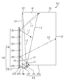
도 4는 본 발명의 다른 실시예에 따른 도광판 및 발광 유닛을 도시한 평면도이다. 도 4에서는 광을 출력하는 발광 유닛(101) 및 상기 광이 입사되는 도광판(550)이 도시되고, 상기 발광 유닛(101)은 도 1에 도시된 표시장치(도 1의 600)의 발광 유닛(도 1의 100)을 대체할 수 있다. 따라서, 도 4를 설명함에 있어서 앞서 설명된 구성요소들에 대해서는 도면부호를 병기하고, 상기 구성요소들에 대한 중복된 설명은 생략된다. 4 is a plan view showing a light guide plate and a light emitting unit according to another embodiment of the present invention. 4, a light-emitting
도 4를 참조하면, 발광 유닛(101)은 인쇄회로기판(PB_1) 및 상기 인쇄회로기판(PB_1)에 실장되는 다수의 발광다이오드들(LG)을 포함한다. 이 실시예에서는, 평면상에서 상기 다수의 발광다이오드들(LG)은 도광판(550)의 제1 면(S1)의 일측부터 타측까지 순차적으로 배열된다. Referring to FIG. 4, the
만약에, 본 발명의 실시예와 달리 상기 발광 유닛(101)이 제1 내지 제5 발광다이오드들(LG1, LG2, LG3, LG4, LG5)로만 구성되는 경우에, 상기 제1 내지 제5 발광다이오드들(LG1, LG2, LG3, LG4, LG5) 각각으로부터 발생되는 광은 약 100도 내지 약 150도의 방사각도로 상기 도광판(550) 내에 제공된다. 이 경우에, 상기 도광판(550)에서 제1 부분(P1) 및 제3 부분(P3)과 같이 상기 제1 내지 제5 발광다이오드들(LG1, LG2, LG3, LG4, LG5) 각각의 위치에 대응하는 부분들 각각에 제공되는 광량을 제1 광량으로 정의하고, 제2 부분(P2) 및 제4 부분(P4)와 같이 상기 제1 내지 제5 발광다이오드들(LG1, LG2, LG3, LG4, LG5) 중 서로 인접한 두 개의 사이에 대응하는 부분들 각각에 제공되는 광량을 제2 광량으로 정의하면, 상기 제2 광량은 상기 제1 광량보다 작을 수 있다. 하지만, 본 발명의 실시예에서는, 상기 발광 유닛(101)은 경사면(SS)과 마주하는 제6 발광다이오드(LG6)를 포함하고, 이에 따라, 상기 제6 발광다이오드(LG6)로부터 발생되어 상기 반사부재(RM)에서 반사되는 제3 광(L3)을 이용하여 상기 제1 광량을 보충할 수 있어 상기 제1 광량 및 상기 제2 광량 간의 편차가 최소화될 수 있다. In a case where the
또한, 상기 제3 광(L3)에 의해 상기 제2 광량뿐만 아니라 상기 제1 광량도 증가할 수 있으나, 상기 제1 및 제3 부분들(P1, P3)에서 상기 발광 유닛(101)으로부터 발생된 광은 상기 제1 면(S1)을 입사할 때 상기 제1 면(S1)에서 산란되고, 이에 따라 상기 제1 및 제3 부분들(P1, P3)은 휘도가 크게 시인될 수 있다. 따라서, 상기 제3 광(L3)에 의해 상기 제1 및 제2 광량이 보충되더라도, 상기 제3 광(L3)에 의해 상기 제1 광량이 보충되는 효과보다 상기 제2 광량이 보충되는 효과가 크므로, 전반적으로 상기 제3 광(L3)에 의해 상기 도광판(550)의 전체 영역에 걸쳐 출력되는 휘도가 균일해지는 효과가 발생될 수 있다. In addition, the first light amount as well as the second light amount can be increased by the third light L3, but it is preferable that the first light amount L3 generated from the
한편, 도 3 및 도 4에 도시되는 실시예들을 비교할 때, 도 4에 도시되는 실시예에서는 상기 제2 및 제4 부분들(P2, P4)에 제공되는 상기 제3 광(L3)의 광량이 증가되도록 상기 경사면(SS) 및 상기 제1 면(S1)이 형성하는 각도(AG)가 도 3에 도시된 실시예의 경우에 비해 작아질 수 있다. 3 and 4, in the embodiment shown in FIG. 4, the light amount of the third light L3 provided to the second and fourth portions P2 and P4 is The angle AG formed by the inclined surface SS and the first surface S1 can be made smaller than that in the embodiment shown in Fig.
도 5는 본 발명의 또 다른 실시예에 따른 도광판 및 발광 유닛을 도시한 평면도이다. 도 5에서는 광을 출력하는 발광 유닛(102) 및 상기 광이 입사되는 도광판(551)이 도시되고, 상기 발광 유닛(102)은 도 1에 도시된 표시장치(도 1의 600)의 발광 유닛(도 1의 100)을 대체할 수 있고, 상기 도광판(551)은 도 1에 도시된 도광판(도 1의 550)을 대체할 수 있다. 도 5를 설명함에 있어서 앞서 설명된 구성요소들에 대해서는 도면부호를 병기하고, 상기 구성요소들에 대한 중복된 설명은 생략된다. 5 is a plan view illustrating a light guide plate and a light emitting unit according to another embodiment of the present invention. 5 shows a
도 5를 참조하면, 발광 유닛(102)은 인쇄회로기판(PB_2) 및 상기 인쇄회로기판(PB_2)에 실장되는 다수의 발광다이오드들(LG)을 포함한다. 도 1에 도시된 실시예에서는 광이 입사되는 제1 면(도 1의 S1)은 도광판(도 1의 500)을 정의하는 단변들 중 어느 하나로 정의되나, 도 5에 도시되는 실시예에서는 광이 입사되는 제1 면(S1)은 상기 도광판(551)을 정의하는 장변들 중 어느 하나로 정의된다. Referring to FIG. 5, the
이 실시예에서도 앞선 실시예들과 마찬가지로, 상기 다수의 발광다이오드들(LG) 중 돌출부(555)에 가장 인접한 제6 발광다이오드(LG6)는 경사면(SS)에 마주하도록 배치되고, 이에 따라, 상기 제6 발광다이오드(LG6)로부터 발생된 제3 광(L3)은 상기 제1 면(S1) 및 상기 경사면(SS)을 순차적으로 투과한 이후에 반사부재(RM)에 반사되어 상기 도광판(551)의 제1 및 제2 부분들(A1, A2) 측으로 제공될 수 있다. 따라서, 상기 도광판(551)의 전체에 걸쳐 균일한 광량이 제공될 수 있고, 이에 따라, 상기 도광판(551)은 전체 영역에 걸쳐 출력되는 광의 휘도가 균일해질 수 있다. In this embodiment, the sixth light emitting diode LG6 closest to the
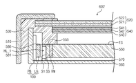
도 6a는 본 발명의 또 다른 실시예에 따른 표시장치의 단면도이고, 도 6b는 도 6a에 도시된 발광 유닛, 도광판, 반사부재 및 표시패널의 결합 상태를 나타내는 분해 사시도이다. 도 6a 및 도 6b에 도시된 표시장치(601)는 도 1 및 도 2a에 도시된 표시 장치(600)에 비해 구성 요소로 이격 부재(ST)를 구성요소로 더 포함한다. 따라서, 도 6a 및 도 6b를 설명함에 있어서, 앞서 도 1, 도 2a, 도 2b 및 도 3을 참조하여 설명된 구성 요소들에 대해서는 도면 부호를 병기하고, 상기 구성 요소들에 대한 중복된 설명은 생략된다. FIG. 6A is a cross-sectional view of a display device according to another embodiment of the present invention, and FIG. 6B is an exploded perspective view illustrating a coupled state of the light emitting unit, the light guide plate, the reflective member, and the display panel shown in FIG. 6A. The
도 6a 및 도 6b를 참조하면, 이 실시예에서 표시 장치(601)는 이격 부재(ST)를 더 포함한다. 상기 이격 부재(ST)는 발광 유닛(100) 및 도광판(550) 사이에 배치되어 상기 발광 유닛(100) 및 상기 도광판(550) 사이의 간격을 유지한다. 또한, 상기 이격 부재(ST)에는 다수의 발광 다이오드들(LG)의 위치에 대응하여 관통홀(HL)이 형성될 수 있고, 이에 따라, 상기 다수의 발광 다이오드들(LG)로부터 발생되는 광은 상기 관통홀(HL) 및 제1 면(S1)을 통해 상기 도광판(550) 측으로 입사될 수 있다. Referring to Figs. 6A and 6B, in this embodiment, the
이 실시예에서, 상기 이격 부재(ST)는 실리콘과 같은 절연성 물질을 포함할 수 있다. 따라서, 상기 인쇄회로기판(PB)로부터 발생되는 열은 상기 도광판(550) 측으로 직접적으로 전달되지 않으므로, 상기 열에 의해 상기 도광판(550)의 형상이 변경되는 것이 방지될 수 있다. In this embodiment, the spacing member ST may comprise an insulating material such as silicon. Therefore, since the heat generated from the printed circuit board PB is not transmitted directly to the
도 7a는 본 발명의 또 다른 실시예에 따른 표시장치의 단면도이고, 도 7b는 도 7a에 도시된 발광 유닛, 도광판, 반사부재, 표시패널 및 수납용기의 결합 상태를 나타내는 분해 사시도이다. 도 7a 및 도 7b에 도시된 표시장치(602)는 도 1 및 도 2a에 도시된 표시 장치(600)에 비해 구성 요소로 이격 부재(586)를 구성요소로 더 포함한다. 따라서, 도 7a 및 도 7b를 설명함에 있어서, 앞서 도 1, 도 2a, 도 2b 및 도 3을 참조하여 설명된 구성 요소들에 대해서는 도면 부호를 병기하고, 상기 구성 요소들에 대한 중복된 설명은 생략된다. FIG. 7A is a cross-sectional view of a display device according to another embodiment of the present invention, and FIG. 7B is an exploded perspective view illustrating a coupled state of the light emitting unit, the light guide plate, the reflective member, the display panel, and the storage container shown in FIG. The
도 7a 및 도 7b를 참조하면, 이 실시예에서 표시 장치(602)는 이격 부재(586)를 더 포함한다. 상기 이격 부재(586)는 발광 유닛(100) 및 도광판(550) 사이에 배치되어 상기 발광 유닛(100) 및 상기 도광판(550) 사이의 간격을 유지시킨다. 또한, 상기 이격 부재(550)에는 다수의 발광 다이오드들(LG)의 위치에 대응하여 관통홀(HL_1)이 형성될 수 있고, 이에 따라, 상기 다수의 발광 다이오드들(LG)로부터 발생되는 광은 상기 관통홀(HL_1) 및 제1 면(S1)을 통해 상기 도광판(550) 측으로 입사될 수 있다. Referring to Figs. 7A and 7B, in this embodiment, the
이 실시예에서, 상기 이격 부재(586)는 수납용기(580)의 바닥부(585)로부터 연장되어 상기 수납용기(580)의 측벽들(581)과 수평일 수 있다. 따라서, 상기 인쇄회로기판(PB)로부터 발생되는 열은 상기 도광판(550) 측으로 직접적으로 전달되지 않고, 상기 열은 상기 이격 부재(586) 측으로 전달되어 상기 수납용기(580)를 통해 외부로 용이하게 방출될 수 있고, 이에 따라, 상기 열에 의해 상기 도광판(550)의 형상이 변경되는 것이 방지될 수 있다. In this embodiment, the spacing
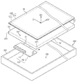
도 8a는 본 발명의 또 다른 실시예에 따른 발광 유닛, 도광판, 및 표시패널의 결합 상태를 나타내는 분해 사시도이고, 도 8b는 도 8a에 도시된 도광판 측으로 입사된 광의 분포를 나타내는 평면도이다. 도 8a 및 도 8b에 도시된 실시예에 도시되는 백라이트 어셈블리는, 도광판(552) 및 발광 유닛(103)을 제외하면, 도 1에 도시된 백라이트 어셈블리(도 1의 500)와 동일한 구성을 갖는다. 따라서, 도 8a 및 도 8b를 설명함에 있어서, 상기 도광판(552) 및 상기 발광 유닛(103)의 구조에 대해 주로 설명하고, 나머지 구성 요소들에 대해서는 도면 부호를 병기하고, 상기 구성 요소들에 대한 중복된 설명은 생략된다. FIG. 8A is an exploded perspective view illustrating a light emitting unit, a light guide plate, and a display panel according to another embodiment of the present invention. FIG. 8B is a plan view illustrating the distribution of light incident on the light guide plate shown in FIG. 8A. The backlight assembly shown in the embodiment shown in Figs. 8A and 8B has the same configuration as the backlight assembly (500 of Fig. 1) shown in Fig. 1, except for the
도 8a 및 도 8b를 참조하면, 상기 발광 유닛(103)은 인쇄회로기판(PB_3) 및 상기 인쇄회로기판(PB_3) 위에 배치된 다수의 발광 다이오드들(LG)을 포함한다. 이 실시예에서는, 상기 인쇄회로기판(PB_3)은 상기 도광판(552)과 수평으로 배치되고, 이에 따라, 상기 인쇄회로기판(PB_3)은 상기 도광판(552) 및 수납용기(580)의 바닥부(585) 사이에 위치할 수 있다. 8A and 8B, the
이 실시예에서는, 상기 인쇄회로기판(PB_3)은 상기 도광판(552)의 제1 코너부(CP1)와 중첩될 수 있다. 상기 도광판(552)이 제1 면(S1), 제2 면(S2), 상기 제1 면(S1)과 마주하는 제3 면(S3) 및 상기 제2 면(S2)과 마주하는 제4 면(S4)을 갖고, 상기 제1 코너부(CP1)는 상기 제1 면(S1) 및 상기 제2 면(S2)이 만나서 정의될 수 있고, 제2 코너부(CP2)는 상기 제1 면(S1) 및 상기 제4 면(S4)이 만나서 정의될 수 있다. In this embodiment, the printed circuit board PB_3 may be overlapped with the first corner portion CP1 of the
이 실시예에서는, 상기 다수의 발광 다이오드들(LG) 중 상기 제1 면(S1)과 마주하는 발광 다이오드는 다수로 제공될 수 있고, 상기 다수의 발광 다이오드들(LG) 중 상기 제2 면(S2)과 마주하는 발광 다이오드는 단수로 제공될 수 있다. 예를 들면, 상기 다수의 발광 다이오드들(LG)이 제1 내지 제6 발광 다이오드들(LG1, LG2, LG3, LG4, LG5, LG6)을 포함한다고 가정할 때, 상기 제1 내지 제5 발광 다이오드들(LG1, LG2, LG3, LG4, LG5)은 상기 제1 면(S1)과 마주하고, 상기 제6 발광 다이오드(LG6)은 상기 제2 면(S2)과 마주한다. 이 경우에, 상기 제1 면(S1)은 제1 방향(D1)으로 연장되고, 상기 제2 면(S2)은 상기 제1 방향(D1)과 실질적으로 수직인 제2 방향(D2)으로 연장되므로, 상기 제1 내지 제5 발광 다이오드들(LG1, LG2, LG3, LG4, LG5) 각각은 상기 제6 발광 다이오드(LG6)과 실질적으로 수직으로 배치될 수 있다. In this embodiment, among the plurality of light emitting diodes LG, a plurality of light emitting diodes facing the first surface S1 may be provided, and the second one of the plurality of light emitting diodes LG, S2 may be provided in singular form. For example, when it is assumed that the plurality of light emitting diodes LG include the first to sixth light emitting diodes LG1, LG2, LG3, LG4, LG5, and LG6, the first to fifth light emitting diodes The first and second light emitting diodes LG1, LG2, LG3, LG4 and LG5 face the first surface S1 and the sixth light emitting diode LG6 faces the second surface S2. In this case the first surface S1 extends in a first direction D1 and the second surface S2 extends in a second direction D2 substantially perpendicular to the first direction D1 Each of the first to fifth light emitting diodes LG1, LG2, LG3, LG4, and LG5 may be disposed substantially perpendicular to the sixth light emitting diode LG6.
상술한 상기 도광판(552) 및 상기 발광 유닛(103)의 구조에 따르면, 상기 제6 발광다이오드(LG6)로부터 발생된 제3 광(L3)은 상기 제2 면(S2)을 통과한 후 상기 도광판(550)의 상기 제2 코너부(CP2) 및 상기 제2 코너부(CP2)의 주변측으로 진행한다. 상기 제2 코너부(CP2) 및 상기 제2 코너부(CP2)의 주변을 제1 부분(A1)으로 정의하면, 상술한 경로를 따라 진행하는 상기 제3 광(L3)에 의해 상기 제1 부분(A1) 측으로 제공되는 제1 광량이 증가할 수 있다. 이에 따라, 상기 제1 광량 및 상기 제1 부분(A1)을 제외한 상기 도광판(550)의 나머지 부분에 제공되는 광량의 차이가 감소될 수 있다. According to the structure of the
또한, 상기 제6 발광 다이오드(LG6)로부터 제공되는 상기 제3 광(L3)의 방사 범위는 상기 제1 코너부(CP1) 및 상기 제1 코너부(CP1)의 주변으로 정의되는 상기 도광판(552)의 제2 부분(A2)을 커버할 수 있으므로, 상기 제2 부분(A2) 측으로 제공되는 광량이 보충될 수도 있다. The emission range of the third light L3 provided from the sixth light emitting diode LG6 may be set to be shorter than the emission angle of the
이상에서는 본 발명의 바람직한 실시예를 참조하여 설명하였지만, 해당 기술 분야의 숙련된 당업자 또는 해당 기술 분야에 통상의 지식을 갖는 자라면, 후술될 특허청구범위에 기재된 본 발명의 사상 및 기술 영역으로부터 벗어나지 않는 범위 내에서 본 발명을 다양하게 수정 및 변경시킬 수 있음을 이해할 수 있을 것이다. 따라서, 본 발명의 기술적 범위는 명세서의 상세한 설명에 기재된 내용으로 한정되는 것이 아니라 특허청구범위에 의해 정하여져야만 할 것이다.While the present invention has been described in connection with what is presently considered to be the most practical and preferred embodiment, it is to be understood that the invention is not limited to the disclosed embodiments, but, on the contrary, It will be understood that various modifications and changes may be made thereto without departing from the scope of the present invention. Therefore, the technical scope of the present invention should not be limited to the contents described in the detailed description of the specification, but should be defined by the claims.
100: 발광 유닛 500: 백라이트 어셈블리
550: 도광판 555: 돌출부
520: 표시패널 600: 표시장치
RM: 반사 부재 PB: 인쇄회로기판
LG: 다수의 발광다이오드들 SS: 경사면
LS: 연결면들100: light emitting unit 500: backlight assembly
550: light guide plate 555:
520: display panel 600: display device
RM: reflective member PB: printed circuit board
LG: a plurality of light emitting diodes SS:
LS: Connection surfaces
Claims (19)
상기 광을 제공받아 영상을 표시하는 표시패널을 포함하고,
상기 백라이트 어셈블리는,
상기 광을 발생하는 발광 유닛;
상기 발광 유닛으로부터 제공된 광을 상기 표시패널 측으로 가이드하고, 측면으로부터 돌출된 돌출부를 갖는 도광판; 및
상기 돌출부의 표면 위에 배치되어 상기 발광 유닛으로부터 상기 돌출부 측으로 제공된 광을 상기 도광판의 코너부 및 상기 코너부의 주변으로 반사시키는 반사 부재를 포함하는 표시 장치. A backlight assembly for outputting light; And
And a display panel for receiving the light and displaying an image,
The backlight assembly includes:
A light emitting unit for emitting the light;
A light guide plate guiding the light provided from the light emitting unit to the display panel side and having a protruding portion projecting from the side surface; And
And a reflective member that is disposed on the surface of the protruding portion and reflects light provided from the light emitting unit toward the protruding portion toward the corner portion of the light guide plate and the periphery of the corner portion.
상기 발광 유닛으로부터 제공된 상기 광이 입사되는 제1 면, 상기 입사된 상기 광이 출사되는 출사면, 상기 제1 면과 대향하는 제2 면, 및 상기 제1 면에 대해 경사진 경사면을 가져 상기 제1 면을 상기 제2 면에 연결하는 연결면들을 포함하고,
상기 경사면은 상기 돌출부의 상기 표면들 중 어느 하나인 것을 특징으로 하는 표시 장치. The light guide plate according to claim 1,
A first surface on which the light provided from the light emitting unit is incident, an exit surface on which the incident light is emitted, a second surface opposed to the first surface, and an inclined surface inclined with respect to the first surface, And connecting surfaces connecting one surface to the second surface,
And the inclined surface is any one of the surfaces of the protruding portion.
상기 제1 면을 따라 신장된 인쇄회로기판; 및
상기 인쇄회로기판 위에서 상기 제1 면을 따라 배열되어 상기 광을 발생하는 다수의 발광다이오드들을 포함하는 것을 특징으로 하는 표시 장치. The light emitting device according to claim 2,
A printed circuit board extending along the first side; And
And a plurality of light emitting diodes arranged along the first surface to generate the light on the printed circuit board.
상기 광을 제공받아 영상을 표시하는 표시패널을 포함하고,
상기 백라이트 어셈블리는,
상기 광을 발생하는 발광 유닛;
상기 발광 유닛으로부터 제공된 광을 상기 표시패널 측으로 가이드하는 도광판을 포함하고,
상기 발광 유닛은,
상기 도광판과 수평으로 배치되어 평면상에서 상기 도광판의 제1 코너부와 중첩되는 인쇄회로기판; 및
상기 인쇄회로기판 위에 배치되고, 상기 제1 코너부를 정의하는 두 측면들을 통해 상기 도광판 측으로 광을 제공하는 다수의 발광 다이오드들을 포함하는 표시 장치. A backlight assembly for outputting light; And
And a display panel for receiving the light and displaying an image,
The backlight assembly includes:
A light emitting unit for emitting the light;
And a light guide plate for guiding the light provided from the light emitting unit to the display panel side,
The light-
A printed circuit board disposed horizontally with the light guide plate and overlapping the first corner of the light guide plate on a plane; And
And a plurality of light emitting diodes disposed on the printed circuit board and providing light to the light guide plate side through two sides defining the first corner.
바닥부 및 상기 바닥부로부터 연장된 측벽들을 구비하여 상기 도광판 및 상기 발광 유닛을 수납하는 수납 용기를 더 포함하고,
상기 인쇄회로기판은 상기 도광판 및 상기 바닥부 사이에 위치하는 것을 특징으로 하는 표시 장치. 14. The method of claim 13,
Further comprising a bottom portion and side walls extending from the bottom portion to accommodate the light guide plate and the light emitting unit,
And the printed circuit board is positioned between the light guide plate and the bottom portion.
Priority Applications (4)
| Application Number | Priority Date | Filing Date | Title |
|---|---|---|---|
| KR1020130007569A KR20140094914A (en) | 2013-01-23 | 2013-01-23 | Dispaly apparatus having backlight assembly |
| US13/905,348 US20140204609A1 (en) | 2013-01-23 | 2013-05-30 | Display device including backlight assembly |
| CN201310349688.XA CN103943041A (en) | 2013-01-23 | 2013-08-12 | Display device |
| JP2013198265A JP2014142590A (en) | 2013-01-23 | 2013-09-25 | Display device |
Applications Claiming Priority (1)
| Application Number | Priority Date | Filing Date | Title |
|---|---|---|---|
| KR1020130007569A KR20140094914A (en) | 2013-01-23 | 2013-01-23 | Dispaly apparatus having backlight assembly |
Publications (1)
| Publication Number | Publication Date |
|---|---|
| KR20140094914A true KR20140094914A (en) | 2014-07-31 |
Family
ID=51190684
Family Applications (1)
| Application Number | Title | Priority Date | Filing Date |
|---|---|---|---|
| KR1020130007569A KR20140094914A (en) | 2013-01-23 | 2013-01-23 | Dispaly apparatus having backlight assembly |
Country Status (4)
| Country | Link |
|---|---|
| US (1) | US20140204609A1 (en) |
| JP (1) | JP2014142590A (en) |
| KR (1) | KR20140094914A (en) |
| CN (1) | CN103943041A (en) |
Families Citing this family (3)
| Publication number | Priority date | Publication date | Assignee | Title |
|---|---|---|---|---|
| CN204141394U (en) * | 2014-09-28 | 2015-02-04 | 北京京东方茶谷电子有限公司 | Backlight module and display unit |
| EP3239592B1 (en) * | 2014-11-18 | 2021-03-31 | Seoul Semiconductor Co., Ltd. | Light emitting device and vehicular lamp comprising same |
| KR102553499B1 (en) * | 2016-07-26 | 2023-07-10 | 삼성전자주식회사 | Display apparatus |
Family Cites Families (25)
| Publication number | Priority date | Publication date | Assignee | Title |
|---|---|---|---|---|
| US6295405B1 (en) * | 1997-07-25 | 2001-09-25 | Physical Optics Corporation | Light pipe for a backlighting system |
| KR100783592B1 (en) * | 2002-02-05 | 2007-12-07 | 삼성전자주식회사 | Illuminating apparatus and display device using the same |
| US6871974B2 (en) * | 2003-06-27 | 2005-03-29 | Matsushita Electric Industrial Co., Ltd. | Lighting unit and liquid crystal device using the same |
| JP4007340B2 (en) * | 2003-09-19 | 2007-11-14 | セイコーエプソン株式会社 | Electro-optical device, electronic apparatus, and method of manufacturing electro-optical device |
| US7894012B2 (en) * | 2005-11-28 | 2011-02-22 | Sharp Kabushiki Kaisha | Backlight device and liquid crystal display device using the same |
| CN100529888C (en) * | 2006-12-22 | 2009-08-19 | 群康科技(深圳)有限公司 | Back light module unit and LCD |
| JP4959506B2 (en) * | 2007-10-31 | 2012-06-27 | 株式会社ジャパンディスプレイイースト | Liquid crystal display |
| JP4939446B2 (en) * | 2008-01-15 | 2012-05-23 | シャープ株式会社 | Surface light source and display device |
| CN101910917B (en) * | 2008-03-25 | 2012-11-21 | 夏普株式会社 | Liquid crystal display device |
| CN101726918B (en) * | 2008-10-29 | 2012-04-11 | 纬创资通股份有限公司 | Display device and electronic device with same |
| CN102282413A (en) * | 2009-01-22 | 2011-12-14 | 夏普株式会社 | Backlight unit and liquid crystal display device |
| TWI402571B (en) * | 2009-04-22 | 2013-07-21 | Advanced Optoelectronic Tech | Backlight module with complementary color zone |
| US20100271841A1 (en) * | 2009-04-27 | 2010-10-28 | Led Folio Corporation | LED Lighting With Light Guide Plate Having Side Reflector |
| TWI380096B (en) * | 2009-05-08 | 2012-12-21 | Au Optronics Corp | Backlight unit |
| KR101546741B1 (en) * | 2009-05-13 | 2015-08-25 | 삼성디스플레이 주식회사 | Light emitting module and display apparatus having the same |
| JP5729581B2 (en) * | 2009-11-12 | 2015-06-03 | Nltテクノロジー株式会社 | Surface emitting device |
| TWI405008B (en) * | 2009-12-04 | 2013-08-11 | Au Optronics Corp | Backlight module and display device having the same |
| TWM381089U (en) * | 2009-12-25 | 2010-05-21 | Coretronic Corp | Backlight module |
| JP2013080562A (en) * | 2010-02-10 | 2013-05-02 | Sharp Corp | Backlight device, liquid crystal display, and television receiver |
| US8786803B2 (en) * | 2010-05-13 | 2014-07-22 | Samsung Display Co., Ltd. | Backlight assembly and display apparatus having the same |
| KR101769971B1 (en) * | 2010-10-29 | 2017-08-22 | 삼성디스플레이 주식회사 | Light guide plate and display device having the same |
| KR101784520B1 (en) * | 2011-03-09 | 2017-10-11 | 엘지디스플레이 주식회사 | Back Light Unit and Liquid Crystal Display Device using the same |
| TWI459093B (en) * | 2011-11-18 | 2014-11-01 | Au Optronics Corp | Backlight module and light source module thereof |
| US20150177446A1 (en) * | 2012-07-24 | 2015-06-25 | Sharp Kabushiki Kaisha | Display device and television device |
| CN104412030B (en) * | 2012-07-24 | 2016-08-24 | 夏普株式会社 | Display device and radiovisor |
-
2013
- 2013-01-23 KR KR1020130007569A patent/KR20140094914A/en not_active Application Discontinuation
- 2013-05-30 US US13/905,348 patent/US20140204609A1/en not_active Abandoned
- 2013-08-12 CN CN201310349688.XA patent/CN103943041A/en active Pending
- 2013-09-25 JP JP2013198265A patent/JP2014142590A/en not_active Withdrawn
Also Published As
| Publication number | Publication date |
|---|---|
| JP2014142590A (en) | 2014-08-07 |
| US20140204609A1 (en) | 2014-07-24 |
| CN103943041A (en) | 2014-07-23 |
Similar Documents
| Publication | Publication Date | Title |
|---|---|---|
| KR102024288B1 (en) | Illumination system using the same | |
| JP6186111B2 (en) | Backlight unit, display device using the same, and illumination system including the same | |
| TWI546593B (en) | Backlight unit and display device using the same | |
| US20120134179A1 (en) | Mosaic light guide plate structure and backlight module | |
| JP2013175460A (en) | Illumination unit and illumination system using the same | |
| KR20120062583A (en) | Backlight unit | |
| JP2013122919A (en) | Illumination unit and display device using the same | |
| KR20140094914A (en) | Dispaly apparatus having backlight assembly | |
| KR101231728B1 (en) | backlight unit and display apparatus using the same | |
| KR101210648B1 (en) | backlight unit and display apparatus using the same | |
| JP2013026211A (en) | Backlight unit and display device using the same | |
| KR101210649B1 (en) | backlight unit and display apparatus using the same | |
| US9052542B2 (en) | Light source package and backlight unit including the light source package | |
| KR101992362B1 (en) | light unit and illumination system using the same | |
| WO2012053262A1 (en) | Lighting apparatus, and display apparatus provided with same | |
| KR20130020302A (en) | Backlight unit and display apparatus using the same | |
| KR101948142B1 (en) | backlight unit and illumination system using the same | |
| US20200264479A1 (en) | Lighting device and display device | |
| KR101963223B1 (en) | Backlight unit, display apparatus using the same, and the lighting apparatus including the same | |
| KR20120134828A (en) | Backlight unit and display apparatus using the same | |
| WO2015002079A1 (en) | Lighting device, display device and television receiving device | |
| KR101902395B1 (en) | illumination unit | |
| KR20130058513A (en) | Backlight unit and illumination system using the same | |
| KR101850429B1 (en) | backlight unit and display apparatus using the same | |
| KR20130046732A (en) | Backlight unit and illumination system using the same |
Legal Events
| Date | Code | Title | Description |
|---|---|---|---|
| WITN | Application deemed withdrawn, e.g. because no request for examination was filed or no examination fee was paid |