KR20140038886A - Light-emitting element - Google Patents
Light-emitting element Download PDFInfo
- Publication number
- KR20140038886A KR20140038886A KR1020130109316A KR20130109316A KR20140038886A KR 20140038886 A KR20140038886 A KR 20140038886A KR 1020130109316 A KR1020130109316 A KR 1020130109316A KR 20130109316 A KR20130109316 A KR 20130109316A KR 20140038886 A KR20140038886 A KR 20140038886A
- Authority
- KR
- South Korea
- Prior art keywords
- layer
- light emitting
- type host
- organic compound
- compound
- Prior art date
Links
Images


Classifications
-
- H—ELECTRICITY
- H10—SEMICONDUCTOR DEVICES; ELECTRIC SOLID-STATE DEVICES NOT OTHERWISE PROVIDED FOR
- H10K—ORGANIC ELECTRIC SOLID-STATE DEVICES
- H10K30/00—Organic devices sensitive to infrared radiation, light, electromagnetic radiation of shorter wavelength or corpuscular radiation
- H10K30/80—Constructional details
- H10K30/865—Intermediate layers comprising a mixture of materials of the adjoining active layers
-
- H—ELECTRICITY
- H10—SEMICONDUCTOR DEVICES; ELECTRIC SOLID-STATE DEVICES NOT OTHERWISE PROVIDED FOR
- H10K—ORGANIC ELECTRIC SOLID-STATE DEVICES
- H10K50/00—Organic light-emitting devices
- H10K50/10—OLEDs or polymer light-emitting diodes [PLED]
- H10K50/11—OLEDs or polymer light-emitting diodes [PLED] characterised by the electroluminescent [EL] layers
- H10K50/135—OLEDs or polymer light-emitting diodes [PLED] characterised by the electroluminescent [EL] layers comprising mobile ions
-
- H—ELECTRICITY
- H10—SEMICONDUCTOR DEVICES; ELECTRIC SOLID-STATE DEVICES NOT OTHERWISE PROVIDED FOR
- H10K—ORGANIC ELECTRIC SOLID-STATE DEVICES
- H10K50/00—Organic light-emitting devices
- H10K50/80—Constructional details
- H10K50/805—Electrodes
-
- H—ELECTRICITY
- H10—SEMICONDUCTOR DEVICES; ELECTRIC SOLID-STATE DEVICES NOT OTHERWISE PROVIDED FOR
- H10K—ORGANIC ELECTRIC SOLID-STATE DEVICES
- H10K2101/00—Properties of the organic materials covered by group H10K85/00
- H10K2101/10—Triplet emission
-
- H—ELECTRICITY
- H10—SEMICONDUCTOR DEVICES; ELECTRIC SOLID-STATE DEVICES NOT OTHERWISE PROVIDED FOR
- H10K—ORGANIC ELECTRIC SOLID-STATE DEVICES
- H10K2101/00—Properties of the organic materials covered by group H10K85/00
- H10K2101/40—Interrelation of parameters between multiple constituent active layers or sublayers, e.g. HOMO values in adjacent layers
-
- H—ELECTRICITY
- H10—SEMICONDUCTOR DEVICES; ELECTRIC SOLID-STATE DEVICES NOT OTHERWISE PROVIDED FOR
- H10K—ORGANIC ELECTRIC SOLID-STATE DEVICES
- H10K2101/00—Properties of the organic materials covered by group H10K85/00
- H10K2101/90—Multiple hosts in the emissive layer
Landscapes
- Physics & Mathematics (AREA)
- Optics & Photonics (AREA)
- Electromagnetism (AREA)
- Electroluminescent Light Sources (AREA)
Abstract
Description
본 발명은 유기 일렉트로루미네선스(EL: Electroluminescence) 현상을 이용한 발광 소자(이하, 유기 EL 소자라고도 기재함)에 관한 것이다.The present invention relates to a light emitting device (hereinafter also referred to as an organic EL device) using an organic electroluminescence (EL) phenomenon.
유기 EL 소자의 연구 개발이 활발히 진행되고 있다. 유기 EL 소자의 기본적인 구성은 한 쌍의 전극간에 발광 물질인 유기 화합물을 포함한 층(이하, 발광층이라고도 기재함)을 끼운 것이다. 유기 EL 소자는 박형 경량화할 수 있거나, 입력 신호에 대하여 고속으로 응답할 수 있거나, 직류 저전압 구동이 가능한 등의 특성이 있으므로 차세대 플랫 패널 디스플레이 소자로서 주목을 받고 있다. 또한 유기 EL 소자를 사용한 디스플레이는 콘트라스트나 화질이 뛰어나고 시야각이 넓다는 특징도 갖는다. 또한 유기 EL 소자는 면 광원이기 때문에 액정 디스플레이의 백 라이트나 조명 등의 광원으로서의 응용도 생각되고 있다.Research and development of organic EL devices are actively progressing. The basic configuration of the organic EL device is a sandwich of an organic compound that is a light emitting material (hereinafter also referred to as a light emitting layer) between a pair of electrodes. The organic EL device has attracted attention as a next-generation flat panel display device because of its characteristics such as thin weight, light weight, high speed response to an input signal, and direct current low voltage driving. In addition, a display using an organic EL element is characterized by excellent contrast and image quality and a wide viewing angle. Moreover, since an organic electroluminescent element is a surface light source, application as a light source, such as a backlight and illumination of a liquid crystal display, is also considered.
유기 EL 소자의 발광 기구는 캐리어 주입형이다. 즉 말하자면 소자에 전압을 인가함으로써 음극으로부터 전자가, 양극으로부터는 정공(홀)이 각각 발광층에 주입되어, 전류가 흐른다. 그리고, 주입된 전자 및 정공이 발광 물질인 유기 화합물을 여기 상태로 도달시킴으로써, 여기된 상기 유기 화합물로부터 발광을 얻는다.The light emitting mechanism of the organic EL element is a carrier injection type. In other words, by applying a voltage to the device, electrons are injected from the cathode and holes (holes) are respectively injected into the light emitting layer from the anode, so that a current flows. Then, light is obtained from the excited organic compound by reaching the excited organic compound with the injected electrons and holes in the excited state.
유기 화합물이 형성하는 여기 상태의 종류로서는 1중항 여기 상태와 3중항 여기 상태가 가능하고, 1중항 여기 상태(S*)로부터의 발광이 형광이라고 불리고, 3중항 여기 상태(T*)로부터의 발광이 인광이라고 불린다. 여기에서, 형광을 발하는 화합물(이하, 형광성 화합물이라고도 기재함)은 실온에 있어서, 일반적으로 인광은 관측되지 않고 형광만이 관측된다. 따라서, 형광성 화합물을 사용한 발광 소자의 내부 양자 효율(주입한 캐리어에 대하여 발생하는 포톤(photon)의 비율)의 이론적 한계는, 상술한 1중항 여기 상태와 3중항 여기 상태의 비율을 근거로 25%라고 생각되고 있다.As the kind of the excited state formed by the organic compound, a singlet excited state and a triplet excited state are possible, and the light emission from the singlet excited state S * is called fluorescence, and the light emission from the triplet excited state T * This is called phosphorescence. Here, a compound which emits fluorescence (hereinafter also referred to as a fluorescent compound) at room temperature generally has no phosphorescence but only fluorescence. Therefore, the theoretical limit of the internal quantum efficiency (the ratio of photons generated to the injected carrier) of the light emitting element using the fluorescent compound is 25% based on the ratio of the singlet excited state and triplet excited state described above. It is thought that.
한편, 인광을 발하는 화합물(이하, 인광성 화합물이라고도 기재함)을 사용하면, 내부 양자 효율을 100%까지 높이는 것이 이론상 가능하게 된다. 즉 말하자면, 형광성 화합물에 비하여 높은 발광 효율을 얻는 것이 가능하게 된다. 이러한 이유에서, 발광 효율이 높은 발광 소자를 실현하기 위하여, 인광성 화합물을 사용한 발광 소자의 개발이 근년에 활발히 진행되고 있다.On the other hand, when a compound which emits phosphorescence (hereinafter also referred to as a phosphorescent compound) is used, it is theoretically possible to increase the internal quantum efficiency to 100%. In other words, it is possible to obtain a high luminous efficiency compared to the fluorescent compound. For this reason, in order to realize a light emitting device having high luminous efficiency, development of a light emitting device using a phosphorescent compound has been actively progressed in recent years.
특히 인광성 화합물로서는 그 인광 양자 수율이 높은 것을 이유로, 이리듐 등을 중심 금속으로 하는 유기 금속 착체가 주목을 받고 있고, 예를 들어 특허문헌 1에는 이리듐을 중심 금속으로 하는 유기 금속 착체가 인광 재료로서 기재되어 있다.Especially as a phosphorescent compound, the organometallic complex which uses iridium etc. as a center metal attracts attention because of its high phosphorescence quantum yield, For example, in
상술한 인광성 화합물을 사용하여 발광 소자의 발광층을 형성하는 경우, 인광성 화합물의 농도 소광(消光)이나 3중항-3중항 소멸에 기인한 소광을 억제하기 위하여 다른 화합물로 이루어지는 매트릭스 중에 상기 인광성 화합물이 분산되도록 형성하는 경우가 많다. 이 때, 매트릭스가 되는 화합물은 호스트, 인광성 화합물과 같이 매트릭스 중에 분산되는 화합물은 게스트라고 각각 불린다.In the case of forming the light emitting layer of the light emitting device using the above-mentioned phosphorescent compound, in order to suppress the quenching caused by the concentration quenching of the phosphorescent compound or the ternary triplet quenching, the phosphorescent compound is formed in a matrix composed of other compounds. It is often formed to disperse a compound. At this time, the compound which becomes a matrix and the compound disperse | distributed in a matrix like a host and a phosphorescent compound are called guest, respectively.
인광성 화합물을 게스트로서 사용하는 발광 소자(이하 인광 발광 소자라고도 기재함)에서의 발광의 일반적인 기본 과정(elementary process)에 대하여 설명한다.A general elementary process of light emission in a light emitting device using a phosphorescent compound as a guest (hereinafter also referred to as a phosphorescent light emitting device) will be described.
(1)직접 재결합 과정(1) direct recombination process
전자 및 정공이 게스트 분자에서 재결합하고 게스트 분자가 여기 상태가 되는 경우, 상기 여기 상태가 3중항 여기 상태일 때 게스트 분자는 인광을 발한다. 상기 여기 상태가 1중항 여기 상태일 때 게스트 분자는 3중항 여기 상태로 항간 교차되어 인광을 발한다.When electrons and holes recombine in the guest molecule and the guest molecule is in an excited state, the guest molecule phosphoresate when the excited state is in the triplet excited state. When the excited state is a singlet excited state, the guest molecule crosses into a triplet excited state and emits phosphorescence.
즉 말하자면 직접 재결합 과정에서는, 게스트 분자의 항간 교차 효율, 및 인광 양자 수율만 높으면, 높은 발광 효율을 얻을 수 있다.In other words, in the direct recombination process, high luminous efficiency can be obtained as long as the intercross efficiency of the guest molecules and the phosphorescent quantum yield are high.
(2)에너지 이동 과정(2) energy transfer process
(2-1)전자 및 정공이 호스트 분자에서 재결합하고 호스트 분자가 3중항 여기 상태가 되는 경우(2-1) When electrons and holes recombine in the host molecule and the host molecule is in triplet excited state
호스트 분자의 3중항 여기 에너지 준위(T1준위)가 게스트 분자의 T1준위보다 높은 경우 호스트 분자로부터 게스트 분자로 여기 에너지가 이동하고, 게스트 분자가 3중항 여기 상태가 된다. 3중항 여기 상태가 된 게스트 분자는 인광을 발한다.When the triplet excitation energy level (T 1 level) of the host molecule is higher than the T 1 level of the guest molecule, the excitation energy is transferred from the host molecule to the guest molecule, and the guest molecule is in the triplet excited state. Guest molecules that are in triplet excited state emit phosphorescence.
(2-2)전자 및 정공이 호스트 분자에서 재결합하고 호스트 분자가 1중항 여기 상태가 되는 경우(2-2) When electrons and holes recombine in the host molecule and the host molecule is in a singlet excited state
호스트 분자의 1중항 여기 에너지 준위(S1준위)가 게스트 분자의 S1준위 및 T1준위보다 높은 경우 호스트 분자로부터 게스트 분자로 여기 에너지가 이동하고, 게스트 분자가 1중항 여기 상태 또는 3중항 여기 상태가 된다. 3중항 여기 상태가 된 게스트 분자는 인광을 발한다. 또한 1중항 여기 상태가 된 게스트 분자는 3중항 여기 상태로 항간 교차되어 인광을 발한다.If the singlet excitation energy level (S 1 level) of the host molecule is higher than the S 1 and T 1 levels of the guest molecule, the excitation energy is transferred from the host molecule to the guest molecule, and the guest molecule is in singlet or triplet excitation. It becomes a state. Guest molecules that are in triplet excited state emit phosphorescence. In addition, the guest molecule which has become a singlet excited state crosses into a triplet excited state and emits phosphorescence.
즉 말하자면, 에너지 이동 과정에 있어서는, 호스트 분자의 3중항 여기 에너지 및 1중항 여기 에너지 쌍방이 얼마나 효율적으로 게스트 분자로 이동할 수 있을지가 중요하다.In other words, in the energy transfer process, it is important how efficiently both the triplet excitation energy and the singlet excitation energy of the host molecule can move to the guest molecule.
이 에너지 이동 과정을 감안하면 호스트 분자로부터 게스트 분자로 여기 에너지가 이동하기 전에 호스트 분자 자체가 그 여기 에너지를 광 또는 열로서 방출하여 불활성화되면 발광 효율이 저하하게 된다.Considering this energy transfer process, the luminous efficiency is lowered if the host molecule itself emits the excitation energy as light or heat and is inactivated before the excitation energy is transferred from the host molecule to the guest molecule.
여기에서 호스트 분자가 1중항 여기 상태인 경우(상기 (2-2))는 3중항 여기 상태인 경우(상기 (2-1))에 비하여 인광성 화합물인 게스트 분자로의 에너지 이동이 발생하기 어렵고 발광 효율이 저하하기 쉽다. 그 이유는 에너지 이동 과정을 고려함으로써 알게 된다.Herein, when the host molecule is in the singlet excited state ((2-2)), energy transfer to the guest molecule, which is a phosphorescent compound, is less likely to occur than in the case of the triplet excited state ((2-1)). Luminous efficiency is easy to fall. The reason is found by considering the energy transfer process.
분자간의 에너지 이동의 기구로서 알려져 있는 푀르스터 기구(쌍극자-쌍극자 상호 작용) 및 덱스터 기구(전자 교환 상호 작용)를 고려하면 호스트로부터 게스트로의 에너지 이동 효율을 높이기(발광 효율이 높은 발광 소자를 실현하기) 위해서는 호스트의 발광 스펙트럼(1중항 여기 상태로부터의 에너지 이동을 논하는 경우에는 형광 스펙트럼, 3중항 여기 상태로부터의 에너지 이동을 논하는 경우에는 인광 스펙트럼)과 게스트의 흡수 스펙트럼(일반적으로는, 인광이기 때문에 3중항 여기 상태와 기저 상태의 에너지 차이)의 중첩이 큰 쪽이 좋다. 또한 게스트의 T1준위로부터 호스트의 T1준위로의 역 에너지 이동을 억제하기 위하여 호스트의 T1준위는 게스트의 T1준위보다 높게 할 필요가 있다.Considering the Usterster mechanism (dipole-dipole interaction) and the dexter mechanism (electron exchange interaction), which are known as mechanisms of energy transfer between molecules, the efficiency of energy transfer from the host to the guest is improved (a light emitting device having high luminous efficiency is realized). The emission spectrum of the host (fluorescence spectrum when discussing the energy transfer from the singlet excited state, phosphorescence spectrum when discussing the energy transfer from the triplet excited state) and the absorption spectrum of the guest (generally, Because of the phosphorescence, the overlap between the triplet excited state and the ground state) is better. In addition, T 1 level of the host in order to suppress the reverse transfer of energy back to the host T 1 level from the T 1 level of the guest may need to be higher than the T 1 level guest.
예를 들어 인광 발광 소자의 게스트로서 사용할 수 있는 인광성 화합물로서, 유기 금속 착체(유기 금속 이리듐 착체 등)를 들 수 있다. 유기 금속 착체는 일반적으로, 비교적 긴 파장의 영역에 3중항 MLCT(Metal to Ligand Charge Transfer) 천이에서 유래하는 흡수대를 갖고, 여기 스펙트럼으로부터도 이 긴 파장 영역(주로 500nm~600nm 부근)의 흡수대가 발광에 크게 기여한다고 할 수 있다. 따라서 이 긴 파장 영역의 흡수대와 호스트의 인광 스펙트럼이 크게 중첩되는 것이 바람직하다. 이것은 호스트의 3중항 여기 상태로부터 효율 좋게 에너지 이동이 일어나 게스트의 3중항 여기 상태가 효율 좋게 생성되기 때문이다.For example, an organometallic complex (organic metal iridium complex etc.) is mentioned as a phosphorescent compound which can be used as a guest of a phosphorescence light emitting element. The organometallic complex generally has an absorption band derived from triplet MLCT (Metal to Ligand Charge Transfer) transition in a relatively long wavelength region, and the absorption band in this long wavelength region (mainly around 500 nm to 600 nm) also emits light from the excitation spectrum. It can be said to contribute greatly to. Therefore, it is preferable that the absorption band of this long wavelength region and the phosphorescence spectrum of a host largely overlap. This is because energy transfer efficiently occurs from the triplet excited state of the host, and the triplet excited state of the guest is efficiently generated.
한편 호스트의 S1준위는 T1준위보다 높기 때문에 S1준위에 대응하는 형광 스펙트럼은 T1준위에 대응하는 인광 스펙트럼에 비하여 매우 짧은 파장 영역에서 관찰된다. 즉 말하자면 이것은 호스트의 형광 스펙트럼과 게스트의 긴 파장 영역의 흡수대(3중항 MLCT 천이에서 유래하는 흡수대)의 중첩이 작게 되는 것을 의미하고, 호스트의 1중항 여기 상태로부터 게스트로의 에너지 이동을 충분히 이용할 수 없게 된다.On the other hand, since the S 1 level of the host is higher than the T 1 level, the fluorescence spectrum corresponding to the S 1 level is observed in a very short wavelength region compared to the phosphorescence spectrum corresponding to the T 1 level. In other words, this means that the superposition of the host's fluorescence spectrum and the guest's long wavelength region (absorption band resulting from triplet MLCT transitions) becomes small, and the energy transfer from the singlet excited state of the host to the guest can be fully utilized. There will be no.
즉 말하자면 종래의 인광 발광 소자는, 호스트의 1중항 여기 상태로부터 게스트로 에너지 이동하여 1중항 여기 상태를 생성하고, 계속되는 항간 교차에 의한 게스트의 3중항 여기 상태의 생성이라는 과정을 거치는 확률이 매우 낮다.In other words, the conventional phosphorescent light emitting device has a very low probability of undergoing a process of generating a singlet excited state by moving energy from the singlet excited state of the host to the guest and generating the triplet excited state of the guest by continuous intersecting of the terms. .
또한 발광 소자에 있어서 상이한 층의 접합을 갖는 경우, 계면에 에너지 갭이 발생하기 때문에 구동 전압이 증대하고 파워 효율이 저하하는 것이 알려져 있다(특허문헌 2 참조).Moreover, in the case of having a junction of different layers in the light emitting device, it is known that the driving voltage increases and the power efficiency decreases because an energy gap occurs at the interface (see Patent Document 2).
본 발명은 이런 문제점을 감안하여 이루어지는 것이다. 본 발명의 일 형태는 발광 효율이 높은 발광 소자를 제공하는 것을 목적 중 하나로 한다.The present invention is made in view of such a problem. An aspect of the present invention is to provide a light emitting device having high light emitting efficiency.
본 발명의 일 형태의 발광 소자는, 제 1 전극과, 제 1 전극 위의 발광층과, 발광층 위의 제 1 층과, 제 1 층 위의 제 2 전극을 갖고, 발광층은 인광성 화합물(게스트라고도 기재함) 및 유기 화합물을 포함하며 인광성 화합물보다 유기 화합물을 많이 포함하고, 제 1 층은 유기 화합물을 포함하고 비행 시간 2차 이온 질량 분석계(Time of Flight-Secondary Ion Mass Spectrometer: ToF-SIMS)에 의한 분석에서는 발광층은 제 1 층보다 유기 화합물의 2차 이온 강도가 높다.The light emitting element of one embodiment of the present invention has a first electrode, a light emitting layer on the first electrode, a first layer on the light emitting layer, and a second electrode on the first layer, and the light emitting layer is a phosphorescent compound (also called a guest). And organic compounds, and more organic compounds than phosphorescent compounds, the first layer comprising organic compounds and a Time of Flight-Secondary Ion Mass Spectrometer (ToF-SIMS). In the analysis by, the light emitting layer has a higher secondary ionic strength of the organic compound than the first layer.
또한 본 발명의 일 형태의 발광 소자는, 제 1 전극과, 제 1 전극 위의 제 1 층과, 제 1 층 위의 발광층과, 발광층 위의 제 2 층과, 제 2 층 위의 제 2 전극을 갖고, 발광층은 인광성 화합물과 제 1 유기 화합물과 제 2 유기 화합물을 포함하며 제 2 유기 화합물을 가장 많이 포함하고, 제 1 층은 제 1 유기 화합물을 포함하고, 제 2 층은 제 2 유기 화합물을 포함하고, 제 1 유기 화합물 및 제 2 유기 화합물은 여기 착체(엑시플렉스, exciplex)를 형성하는 조합이고, ToF-SIMS에 의한 분석에서는 제 1 층, 발광층, 및 제 2 층 중에서 제 2 유기 화합물의 2차 이온 강도가 가장 높은 층은 발광층이고, 다음에 높은 층은 제 2 층이며, 가장 낮은 층은 제 1 층이다.In addition, the light emitting device of one embodiment of the present invention includes a first electrode, a first layer on the first electrode, a light emitting layer on the first layer, a second layer on the light emitting layer, and a second electrode on the second layer. Wherein the light emitting layer comprises a phosphorescent compound, a first organic compound and a second organic compound, the second organic compound is the most abundant, the first layer comprises a first organic compound, and the second layer is a second organic compound. Wherein the first organic compound and the second organic compound are combinations that form an exciplex (exiplex), and in the analysis by ToF-SIMS, the second organic compound among the first layer, the light emitting layer, and the second layer The layer with the highest secondary ionic strength of the compound is the light emitting layer, followed by the high layer is the second layer and the lowest layer is the first layer.
또한 본 발명의 다른 형태의 발광 소자는, 제 1 전극과, 제 1 전극 위의 제 1 층과, 제 1 층 위의 발광층과, 발광층 위의 제 2 층과, 제 2 층 위의 제 2 전극을 갖고, 발광층은 인광성 화합물과, 정공 수송성을 갖는 제 1 유기 화합물과, 전자 수송성을 갖는 제 2 유기 화합물을 포함하고, 제 1 층은 제 1 유기 화합물을 포함하고, 제 2 층은 제 2 유기 화합물을 포함하고, 제 1 유기 화합물 및 제 2 유기 화합물은 여기 착체를 형성하는 조합이고, ToF-SIMS에 의한 분석에서는 제 1 층, 발광층, 및 제 2 층 중에서 제 2 유기 화합물의 2차 이온 강도가 가장 높은 층은 발광층이고, 다음에 높은 층은 제 2 층이며, 가장 낮은 층은 제 1 층이다.In another embodiment, a light emitting device includes a first electrode, a first layer on a first electrode, a light emitting layer on a first layer, a second layer on a light emitting layer, and a second electrode on a second layer. Wherein the light emitting layer comprises a phosphorescent compound, a first organic compound having hole transport properties, and a second organic compound having electron transport properties, the first layer comprising a first organic compound, and the second layer having a second layer An organic compound, wherein the first organic compound and the second organic compound are combinations that form an exciplex, and in the analysis by ToF-SIMS, secondary ions of the second organic compound in the first layer, the light emitting layer, and the second layer The layer with the highest intensity is the light emitting layer, the next higher layer is the second layer, and the lowest layer is the first layer.
본 발명의 일 형태의 발광 소자에서, ToF-SIMS에 의한 분석에서는 제 1 층, 발광층, 및 제 2 층 중에서 제 1 유기 화합물의 2차 이온 강도가 가장 낮은 층은 제 2 층이면 바람직하다.In the light emitting device of one embodiment of the present invention, in the analysis by ToF-SIMS, the layer having the lowest secondary ionic strength of the first organic compound among the first layer, the light emitting layer, and the second layer is preferably the second layer.
본 명세서에서는 제 1 유기 화합물 및 제 2 유기 화합물의 정공 수송성 또는 전자 수송성의 특색에 주목하여 정공 수송성을 갖는 유기 화합물을 P형 호스트, 전자 수송성을 갖는 유기 화합물을 N형 호스트라고도 기재한다.In the present specification, paying attention to the characteristics of the hole transporting or electron transporting properties of the first organic compound and the second organic compound, the organic compound having hole transporting properties is also described as a P type host, and the organic compound having electron transporting properties is also referred to as an N type host.
상기 발광 소자에서는 여기 착체로부터 인광성 화합물로의 에너지 이동을 거쳐 인광성 화합물이 여기되고, 인광성 화합물의 여기 상태로부터의 발광을 얻을 수 있다. 또한 발광층 이외의 층이 전류의 주입에 의하여 발광하는 능력을 가져도 좋다.In the above light emitting device, the phosphorescent compound is excited through energy transfer from the exciplex to the phosphorescent compound, and light emission from the excited state of the phosphorescent compound can be obtained. Further, layers other than the light emitting layer may have the ability to emit light by injection of electric current.
여기 착체는 1중항 여기 에너지와 3중항 여기 에너지의 차이가 매우 작다고 생각된다. 바꿔 말하면 여기 착체의 1중항 상태로부터의 발광과 3중항 상태로부터의 발광은 매우 가까운 파장 영역에 나타난다. 또한 여기 착체의 발광은 일반적인 모노머 상태와 비교하여 긴 파장 측에 관찰되기 때문에 긴 파장 영역에 나타나는 인광성 화합물의 3중항 MLCT 천이에서 유래하는 흡수와, 여기 착체의 발광의 중첩을 크게 할 수 있다. 즉 말하자면 이것은 여기 착체의 1중항 상태 및 3중항 상태의 쌍방으로부터 인광성 화합물에 대하여 효율적으로 에너지 이동할 수 있다는 것을 의미하고 발광 소자의 발광 효율을 향상시키는 것이 된다.The complex here is thought to have a very small difference between singlet excitation energy and triplet excitation energy. In other words, the light emission from the singlet state and the light emission from the triplet state of the exciplex are shown in a very close wavelength region. In addition, since the light emission of the exciplex is observed on the long wavelength side as compared with the general monomer state, the absorption derived from the triplet MLCT transition of the phosphorescent compound appearing in the long wavelength region and the light emission of the exciplex can be increased. In other words, this means that energy can be efficiently transferred to the phosphorescent compound from both the singlet state and triplet state of the exciplex, thereby improving the luminous efficiency of the light emitting element.
또한, 여기 착체에는 기저 상태가 존재하지 않는다. 따라서 인광성 화합물의 3중항 여기 상태로부터 여기 착체로 역 에너지 이동하는 과정은 존재하지 않기 때문에 이 과정에 의한 발광 소자의 발광 효율은 저하되지 않는다.In addition, no ground state exists in the complex here. Therefore, since there is no process of reverse energy transfer from the triplet excited state of the phosphorescent compound to the exciplex, the luminous efficiency of the light emitting device by this process does not decrease.
또한 적절한 P형 호스트 및 N형 호스트의 조합으로서는, P형 호스트 및/또는 N형 호스트가 여기 상태가 되었을 때, 여기 착체를 형성한다. 또한 여기 착체를 형성하는 필요 조건으로서는 N형 호스트의 HOMO준위<P형 호스트의 HOMO준위<N형 호스트의 LUMO준위<P형 호스트의 LUMO준위이지만 이것은 충분 조건이 아니다. 예를 들어 P형 호스트를 NPB, N형 호스트를 Alq3으로 하면 상기 조건을 충족시키지만 여기 착체를 형성할 수는 없다.As a suitable combination of the P-type host and the N-type host, an exciplex is formed when the P-type host and / or the N-type host are in an excited state. In addition, as a necessary condition for forming the exciplex, the HOMO level of the N-type host <HOMO level of the P-type host <LUMO level of the N-type host <LUMO level of the P-type host, but this is not sufficient. For example, if the P-type host is NPB and the N-type host is Alq 3 , the above conditions are satisfied, but the excitation complex cannot be formed.
이에 대하여 P형 호스트 및 N형 호스트가 여기 착체를 형성할 수 있는 경우에는 상술한 바와 같이 여기 착체의 1중항 상태와 3중항 상태의 쌍방으로부터 인광성 화합물로 에너지 이동이 발생하고, 이에 따라 인광성 화합물을 여기시키는 것이 가능하기 때문에 종래의 인광 발광 소자에 비하여 발광 효율이 향상된다.On the other hand, when the P-type host and the N-type host can form an exciplex, as described above, energy transfer occurs from both the singlet and triplet states of the exciplex to the phosphorescent compound. Since the compound can be excited, the luminous efficiency is improved as compared with the conventional phosphorescent light emitting device.
또한 발광 소자에서의 이종 재료의 접합을 줄임으로써 계면에 에너지 갭이 발생하여 구동 전압이 증대하거나 파워 효율이 저하하는 것을 억제할 수 있어 바람직하다.In addition, by reducing the bonding of dissimilar materials in the light emitting device, an energy gap is generated at the interface, which can suppress an increase in driving voltage or a decrease in power efficiency.
본 발명의 일 형태의 발광 소자에 있어서 발광층과 제 2 층의 계면에서는 정공에 대하여 장해가 되는 반면에, 전자에 대해서는 거의 장해가 없고, 또한 발광층과 제 1 층의 계면에서는 전자에 대하여 장해가 되는 반면에, 정공에 대해서는 거의 장해가 없다. 그러므로 전자와 정공은 발광층 내 또는 제 1 층과 제 2 층 사이에 갇힌다. 이 결과, 전자가 양극까지 도달하거나 정공이 음극까지 도달하는 것을 억제할 수 있으므로 발광 효율의 저하를 억제할 수 있다.In the light emitting device of one embodiment of the present invention, at the interface between the light emitting layer and the second layer, obstacles are caused to holes, while there are almost no obstacles to electrons, and at the interface of the light emitting layer and the first layer, the electrons are disturbed. On the other hand, there is almost no obstacle to the hole. Therefore, electrons and holes are trapped in the light emitting layer or between the first and second layers. As a result, it is possible to suppress the electrons reaching the anode and the holes reaching the cathode, thereby suppressing the decrease in luminous efficiency.
또한 여기 착체는 일반적으로 넓은 발광 스펙트럼을 주지만, 본 발명의 일 형태에서는 인광성 화합물이 발광하기 때문에 반값폭이 좁은 스펙트럼을 얻을 수 있고 결과적으로 발광의 색 순도가 높은 발광 소자를 얻을 수 있다.In addition, although the exciplex generally gives a wide emission spectrum, in one embodiment of the present invention, since the phosphorescent compound emits light, a spectrum having a narrow half-value width can be obtained, and as a result, a light emitting device having high color purity of light emission can be obtained.
본 발명의 일 형태의 발광 소자는 발광층에 인광성 화합물과, 제 1 유기 화합물과, 제 2 유기 화합물을 포함하며 상기 제 2 유기 화합물을 가장 많이 포함한다. 본 발명의 일 형태의 발광 소자가 갖는 제 1 층, 발광층, 및 제 2 층 중에서 제 2 유기 화합물이 가장 많이 포함되는 층(체적분율 또는 mol분율이 가장 높은 층)은 제 2 층이고, 다음에 많이 포함되는 층은 발광층이다. 그러나 본 발명의 일 형태의 발광 소자를 ToF-SIMS에 의하여 분석하면 발광층에서의 제 2 유기 화합물의 함유량이 적은 것에 비하여 제 2 유기 화합물의 2차 이온 강도는 높다는 현상을 나타낸다. 상술한 바와 같이 본 발명의 일 형태의 발광 소자에서, 제 1 층, 발광층, 및 제 2 층 중 제 2 유기 화합물의 2차 이온 강도가 가장 높은 층은 발광층이고, 다음에 높은 층은 제 2 층이다.The light emitting element of one embodiment of the present invention includes a phosphorescent compound, a first organic compound, and a second organic compound in the light emitting layer, and most includes the second organic compound. Among the first layer, the light emitting layer, and the second layer of the light emitting device of one embodiment of the present invention, the layer containing the second most organic compound (the layer having the highest volume fraction or mol fraction) is the second layer, and then A lot of layers are light emitting layers. However, analysis of the light-emitting device of one embodiment of the present invention by ToF-SIMS shows a phenomenon that the secondary ionic strength of the second organic compound is higher than that of the second organic compound in the light emitting layer is small. In the light emitting device of one embodiment of the present invention as described above, the layer having the highest secondary ionic strength of the second organic compound among the first layer, the light emitting layer, and the second layer is the light emitting layer, and the next high layer is the second layer. to be.
ToF-SIMS를 사용한 분석에서는, 어느 층에 포함되는 재료의 2차 이온 강도가 높으면 상기 재료는 이온화될 때 분자가 붕괴되기 어렵다고 할 수 있다. 따라서 본 발명의 일 형태의 발광 소자에 전류를 흘려도 발광층에 포함되는 제 2 유기 화합물의 분자는, 단독으로 존재하는 경우에 비하여 붕괴되기 어렵다는 것이 시사된다. 따라서 본 발명의 일 형태를 적용함으로써 긴 수명의 발광 소자를 실현할 수 있다.In the analysis using ToF-SIMS, if the secondary ionic strength of a material included in a layer is high, it can be said that the material hardly collapses when the material is ionized. Therefore, even if an electric current flows through the light emitting element of one embodiment of the present invention, it is suggested that the molecules of the second organic compound included in the light emitting layer are less likely to collapse compared to the case in which they exist alone. Therefore, by applying one embodiment of the present invention, a light emitting device having a long lifetime can be realized.
또한 본 발명의 다른 형태의 발광 소자는, 발광층에 게스트, P형 호스트, 및 N형 호스트를 포함한다. 본 발명의 일 형태의 발광 소자가 갖는 제 1 층, 발광층, 및 제 2 층 중에서 N형 호스트가 가장 많이 포함되는 층(체적분율 또는 mol분율이 가장 높은 층)은 제 2 층이고, 다음에 많이 포함되는 층은 발광층이다. 그러나 본 발명의 일 형태의 발광 소자를 ToF-SIMS에 의하여 분석하면 발광층에서의 N형 호스트의 함유량이 적은 것에 비하여 N형 호스트의 2차 이온 강도가 높다는 현상을 나타낸다. 상술한 바와 같이 본 발명의 일 형태의 발광 소자에서, 제 1 층, 발광층, 및 제 2 층 중 N형 호스트의 2차 이온 강도가 가장 높은 층은 발광층이고, 다음에 높은 층은 제 2 층이다. 따라서 본 발명의 일 형태의 발광 소자에 전류를 흘려도 발광층에 포함되는 N형 호스트 분자는, 단독으로 존재하는 경우에 비하여 붕괴되기 어렵다는 것이 시사된다. 따라서 본 발명의 일 형태를 적용함으로써 긴 수명의 발광 소자를 실현할 수 있다.Another embodiment of the light-emitting device of the present invention includes a guest, a P-type host, and an N-type host in the light emitting layer. Among the first layer, the light emitting layer, and the second layer of the light emitting device of one embodiment of the present invention, the layer containing the most N-type host (the layer having the highest volume fraction or mol fraction) is the second layer, and many The layer included is a light emitting layer. However, analysis of the light-emitting device of one embodiment of the present invention by ToF-SIMS shows a phenomenon that the secondary ionic strength of the N-type host is higher than that of the N-type host in the light emitting layer. In the light emitting device of one embodiment of the present invention as described above, the layer having the highest secondary ionic strength of the N-type host among the first layer, the light emitting layer, and the second layer is the light emitting layer, and the next high layer is the second layer. . Therefore, even if an electric current flows through the light emitting element of one embodiment of the present invention, it is suggested that the N-type host molecule contained in the light emitting layer is less likely to collapse than the case in which it is present alone. Therefore, by applying one embodiment of the present invention, a light emitting device having a long lifetime can be realized.
특히 P형 호스트에 방향족 아민 화합물을 사용하는 것이 바람직하다. 또한 N형 호스트에 질소 함유 복소 방향족 화합물을 사용하는 것이 바람직하다. 또한 N형 호스트에 6원 고리의 헤테로 방향족 화합물을 사용하는 것이 바람직하다. 특히 N형 호스트가 다이아진 고리를 갖는 것이 바람직하다.In particular, it is preferable to use an aromatic amine compound for the P-type host. It is also preferable to use a nitrogen-containing heteroaromatic compound for the N-type host. It is also preferable to use a heteroaromatic compound of 6 membered ring for the N-type host. It is particularly preferred for the N-type host to have a azine ring.
P형 호스트, N형 호스트 중 어느 한쪽은 형광성 화합물이어도 좋다. 또한 발광층 내의 P형 호스트의 농도 및 N형 호스트의 농도는 각각 10% 이상인 것이 바람직하다.A fluorescent compound may be sufficient as either a P type host or an N type host. The concentration of the P-type host and the N-type host in the light emitting layer is preferably 10% or more, respectively.
또한 상기 발광 소자에서, 인광성 화합물은 유기 금속 착체인 것이 바람직하다. 인광성 화합물은 발광층 이외에 제 1 층 또는 제 2 층, 또는 발광층과 제 1 층 사이의 영역이나 발광층과 제 2 층 사이의 영역에 포함되어도 좋다.In the above light emitting device, the phosphorescent compound is preferably an organometallic complex. The phosphorescent compound may be included in the region between the first layer or the second layer, or the region between the emitting layer and the first layer, or the region between the emitting layer and the second layer, in addition to the emitting layer.
본 발명의 일 형태에서는, 발광층은 P형 호스트 분자, N형 호스트 분자, 및 게스트 분자를 갖는다. 물론 분자는 규칙적으로 배열할 필요는 없고 규칙성이 매우 적은 상태이어도 좋다. 특히 발광층을 50nm 이하의 박막으로 하는 경우에는 비정질 상태가 되는 것이 바람직하고, 그러므로 결정화되기 어려운 재료의 조합을 선택하는 것이 바람직하다. 또한 P형 호스트를 포함한 층이나 N형 호스트를 포함한 층은 2종류 이상의 다른 화합물을 포함하여도 좋다.In one embodiment of the present invention, the light emitting layer has a P-type host molecule, an N-type host molecule, and a guest molecule. Of course, the molecules do not have to be arranged regularly and may be in a state of very low regularity. In particular, in the case where the light emitting layer is a thin film of 50 nm or less, it is preferable to be in an amorphous state, and therefore, it is preferable to select a combination of materials that are difficult to crystallize. In addition, the layer containing a P-type host or the layer containing an N-type host may contain two or more types of different compounds.
본 발명의 일 형태의 발광 소자는 발광 장치, 전자 기기, 및 조명 장치에 적용할 수 있다. 본 발명의 일 형태의 발광 소자는 발광 효율이 높으므로 소비 전력이 낮은 발광 장치, 전자 기기, 및 조명 장치를 실현할 수 있다.The light emitting element of one embodiment of the present invention can be applied to a light emitting device, an electronic device, and a lighting device. Since the light emitting element of one embodiment of the present invention has high luminous efficiency, a light emitting device, an electronic device, and a lighting device having low power consumption can be realized.
본 발명의 일 형태의 발광 소자는 P형 호스트를 포함한 층과, 게스트, P형 호스트, 및 N형 호스트를 포함한 발광층과, N형 호스트를 포함한 층을 갖는다. P형 호스트 및 N형 호스트는 여기 착체를 형성하는 조합이기 때문에 본 발명의 일 형태에서는 캐리어를 가두는 것과 발광층으로의 캐리어 주입 장벽의 저감이 동시에 달성될 뿐만 아니라, 여기 착체를 형성하고 그 1중항 여기 상태와 3중항 여기 상태의 쌍방으로부터의 에너지 이동 과정을 이용할 수 있으므로 발광 효율이 높은 발광 소자를 실현할 수 있다.The light emitting element of one embodiment of the present invention has a layer containing a P-type host, a light emitting layer containing a guest, a P-type host, and an N-type host, and a layer containing an N-type host. Since the P-type host and the N-type host are combinations that form an exciplex, in one embodiment of the present invention, not only the carrier confinement and the reduction of the carrier injection barrier to the light emitting layer are simultaneously achieved, but also the exciplex is formed and the singlet thereof. Since the energy transfer process from both the excited state and the triplet excited state can be used, a light emitting device having high luminous efficiency can be realized.
도 1은 본 발명의 일 형태의 개념도.
도 2는 본 발명의 일 형태의 원리를 설명한 도면.
도 3은 발광 소자의 일례를 도시한 도면.
도 4는 발광 소자를 제조하기 위한 장치의 일례를 도시한 도면.
도 5는 발광 장치의 일례를 도시한 도면.
도 6은 발광 장치의 일례를 도시한 도면.
도 7은 전자 기기의 일례를 도시한 도면.
도 8은 조명 장치의 일례를 도시한 도면.
도 9는 실시예 1에 관한 흡수 스펙트럼 및 광루미네선스(photoluminescence)·스펙트럼을 나타낸 도면.
도 10은 실시예 1에 관한 흡수 스펙트럼 및 광루미네선스·스펙트럼을 나타낸 도면.
도 11은 실시예의 발광 소자를 설명한 도면.
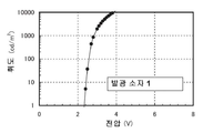
도 12는 실시예 2의 발광 소자의 전류 밀도-휘도 특성을 나타낸 도면.
도 13은 실시예 2의 발광 소자의 전압-휘도 특성을 나타낸 도면.
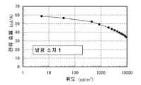
도 14는 실시예 2의 발광 소자의 휘도-전류 효율 특성을 나타낸 도면.
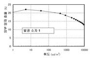
도 15는 실시예 2의 발광 소자의 휘도-외부 양자 효율 특성을 나타낸 도면.
도 16은 실시예 2의 발광 소자의 발광 스펙트럼을 나타낸 도면.
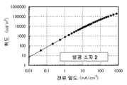
도 17은 실시예 2의 발광 소자의 ToF-SIMS에 의한 측정 결과를 나타낸 도면.
도 18은 실시예 3의 발광 소자의 전류 밀도-휘도 특성을 나타낸 도면.
도 19는 실시예 3의 발광 소자의 전압-휘도 특성을 나타낸 도면.
도 20은 실시예 3의 발광 소자의 휘도-전류 효율 특성을 나타낸 도면.
도 21은 실시예 3의 발광 소자의 휘도-외부 양자 효율 특성을 나타낸 도면.
도 22는 실시예 3의 발광 소자의 발광 스펙트럼을 나타낸 도면.
도 23은 실시예 3의 발광 소자의 ToF-SIMS에 의한 측정 결과를 나타낸 도면.
도 24는 실시예 3의 발광 소자의 신뢰성 시험의 결과를 나타낸 도면.1 is a conceptual diagram of one embodiment of the present invention.
2 is a view for explaining the principle of one embodiment of the present invention.
3 shows an example of a light emitting element;
4 shows an example of an apparatus for manufacturing a light emitting element.
5 illustrates an example of a light emitting device.
6 illustrates an example of a light emitting device.
7 illustrates an example of an electronic device.
8 shows an example of a lighting device.
9 is a diagram showing an absorption spectrum and a photoluminescence spectrum according to Example 1. FIG.
10 is a diagram showing an absorption spectrum and a photoluminescence spectrum according to Example 1;
11 is a view for explaining a light emitting element of the embodiment;
12 is a diagram showing the current density-luminance characteristics of the light emitting device of Example 2;
13 shows voltage-luminance characteristics of the light emitting device of Example 2;
Fig. 14 is a graph showing the luminance-current efficiency characteristics of the light emitting device of Example 2;
Fig. 15 is a graph showing the luminance-external quantum efficiency characteristics of the light emitting device of Example 2;
16 is a diagram showing an emission spectrum of the light emitting device of Example 2. Fig.
17 shows measurement results by ToF-SIMS of the light emitting device of Example 2;
18 is a diagram showing the current density-luminance characteristics of the light emitting device of Example 3;
19 is a diagram showing the voltage-luminance characteristics of the light emitting device of Example 3;
20 shows luminance-current efficiency characteristics of the light emitting device of Example 3;
Fig. 21 is a graph showing the luminance-external quantum efficiency characteristics of the light emitting device of Example 3;
22 is a diagram showing an emission spectrum of the light emitting device of Example 3. Fig.
FIG. 23 is a view showing a measurement result by ToF-SIMS of a light emitting device of Example 3; FIG.
24 is a diagram showing the results of a reliability test of the light emitting device of Example 3;
실시형태에 대하여, 도면을 사용하여 상세하게 설명한다. 다만, 본 발명은 이하의 설명에 한정되지 아니하며, 본 발명의 취지 및 그 범위에서 벗어남이 없이 그 형태 및 상세한 사항을 다양하게 변경할 수 있는 것은 당업자이면 용이하게 이해할 수 있다. 따라서, 본 발명은 이하에 나타내는 실시형태의 기재 내용에 한정하여 해석되는 것은 아니다. 또한, 이하에 설명하는 발명의 구성에 있어서, 동일 부분 또는 같은 기능을 가지는 부분에는 동일한 부호를 다른 도면간에서 공통적으로 사용하고, 그 반복 설명은 생략한다.EMBODIMENT OF THE INVENTION Embodiment is described in detail using drawing. However, the present invention is not limited to the following description, and it can be easily understood by those skilled in the art that various changes can be made in form and detail without departing from the spirit and scope of the present invention. Therefore, the present invention is not construed as being limited to the description of the embodiments described below. In addition, in the structure of the invention demonstrated below, the same code | symbol is used in common between different figures for the same part or the part which has the same function, and the repeated description is abbreviate | omitted.
(실시형태 1)(Embodiment 1)
본 실시형태에서는 본 발명의 일 형태의 발광 소자에 대하여 도 1 및 도 2를 사용하여 설명하기로 한다.In this embodiment, a light emitting device of one embodiment of the present invention will be described with reference to FIGS. 1 and 2.
본 발명의 일 형태의 발광 소자는, 한 쌍의 전극(제 1 전극 및 제 2 전극) 사이에 발광성을 갖는 유기 화합물을 포함한 층(EL층)을 갖는다. 한 쌍의 전극 중 한쪽은 양극으로서 기능하고, 다른 쪽은 음극으로서 기능한다. EL층은 제 1 전극 위의 제 1 층과, 제 1 층 위의 발광층과, 발광층 위의 제 2 층을 갖는다. 상기 발광층은 인광성 화합물(게스트), 제 1 유기 화합물, 및 제 2 유기 화합물을 갖고, 상기 제 2 유기 화합물을 가장 많이 포함한다. 제 1 층은 제 1 유기 화합물을 포함하고, 상기 제 2 유기 화합물을 포함하지 않는다. 제 2 층은 상기 제 2 유기 화합물을 포함하고 상기 제 1 유기 화합물을 포함하지 않는다. 제 1 유기 화합물 또는 제 2 유기 화합물 중 한쪽은 정공 수송성을 갖는 유기 화합물(P형 호스트)이고, 다른 쪽은 전자 수송성을 갖는 유기 화합물(N형 호스트)이다. 그리고 P형 호스트 및 N형 호스트는 여기 착체를 형성하는 조합이다.The light emitting element of one embodiment of the present invention has a layer (EL layer) containing an organic compound having luminescence between a pair of electrodes (first electrode and second electrode). One of the pair of electrodes functions as an anode and the other function as a cathode. The EL layer has a first layer on the first electrode, a light emitting layer on the first layer, and a second layer on the light emitting layer. The light emitting layer has a phosphorescent compound (guest), a first organic compound, and a second organic compound, and most contains the second organic compound. The first layer comprises a first organic compound and does not contain the second organic compound. The second layer includes the second organic compound and does not include the first organic compound. One of a 1st organic compound or a 2nd organic compound is an organic compound (P type host) which has hole transport property, and the other is an organic compound (N type host) which has electron transport property. And the P-type host and the N-type host are combinations forming an exciplex.
본 발명의 일 형태의 발광 소자가 갖는 제 1 층, 발광층, 및 제 2 층 중 제 1 유기 화합물이 가장 많이 포함되는 층(체적분율 또는 mol분율이 가장 높은 층)은 제 1 층이고, 다음에 많이 포함되는 층은 발광층이고, 제 2 층에는 제 1 유기 화합물이 포함되지 않는다. 한편 제 2 유기 화합물이 가장 많이 포함되는 층(체적분율 또는 mol분율이 가장 높은 층)은 제 2 층이고, 다음에 많이 포함되는 층은 발광층이고, 제 1 층에는 제 2 유기 화합물이 포함되지 않는다. 그러나 본 발명의 일 형태의 발광 소자를 ToF-SIMS에 의하여 분석하면, 발광층에서의 제 1 유기 화합물이나 제 2 유기 화합물의 함유량이 적은 것에 비하여 제 1 유기 화합물이나 제 2 유기 화합물의 2차 이온 강도는 높다는 현상을 나타낸다.The layer (highest volume fraction or the highest mol fraction) of the first layer, the light emitting layer, and the second layer included in the light emitting device of one embodiment of the present invention is the first layer, and then A large amount of the layer is a light emitting layer, and the second layer does not contain the first organic compound. On the other hand, the layer containing the largest amount of the second organic compound (the layer having the highest volume fraction or mol fraction) is the second layer, the next containing layer is the light emitting layer, and the first layer does not contain the second organic compound. . However, when the light emitting device of one embodiment of the present invention is analyzed by ToF-SIMS, the secondary ionic strength of the first organic compound or the second organic compound is lower than that of the first organic compound or the second organic compound in the light emitting layer. Indicates a phenomenon of high.
EL층은 정공 주입성이 높은 물질, 정공 수송성이 높은 물질, 전자 수송성이 높은 물질, 전자 주입성이 높은 물질, 또는 바이폴러성의 물질(전자 수송성 및 정공 수송성이 높은 물질) 등을 포함한 층을 추가로 가져도 좋다.The EL layer further includes a layer containing a material having a high hole injection property, a material having a high hole transport property, a material having a high electron transport property, a material having a high electron injection property, or a bipolar material (a material having high electron transport and hole transport properties). You may bring it.
EL층에는 저분자계 화합물 및 고분자계 화합물 중 어느 것을 사용할 수도 있고, 무기 화합물을 포함하여도 좋다.Either a low molecular weight compound and a high molecular type compound may be used for an EL layer, and an inorganic compound may be included.
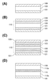
도 1의 (A)에 EL층이 구비한 적층체의 일례를 도시하였다. 도 1의 (A)에 도시된 적층체(100a)는 양극 측으로부터 P형 호스트를 포함한 층(103), 발광층(102), 및 N형 호스트를 포함한 층(104)을 갖는다.An example of the laminated body with which an EL layer was shown in FIG. The laminate 100a shown in Fig. 1A has a
발광층(102)은 게스트(105), P형 호스트, 및 N형 호스트를 포함한다. 본 실시형태에서, 게스트(105)는 인광성 화합물이고, 발광층(102)에 분산된다. 여기서 P형 호스트는 정공 수송성을 갖는 유기 화합물이고, N형 호스트는 전자 수송성을 갖는 유기 화합물이다. 또한 상기 P형 호스트 및 상기 N형 호스트는 여기 착체를 형성하는 조합이다.The
P형 호스트를 포함한 층(103)은 P형 호스트를 포함하고 N형 호스트를 포함하지 않는다(본 명세서 중에서는 N형 호스트의 농도가 0.1% 이하인 것을 가리킨다).The
N형 호스트를 포함한 층(104)은 N형 호스트를 포함하고 P형 호스트를 포함하지 않는다(본 명세서 중에서는 P형 호스트의 농도가 0.1% 이하인 것을 가리킨다).The
도 1의 (B)에, 도 1의 (A)에 도시된 적층체(100a)에서의 P형 호스트의 농도(도면 중에서 P라고 표기함), 및 N형 호스트의 농도(도면 중에서 N이라고 표기함)의 분포를 도시하였다. 도 1의 (B)에서는 발광층(102) 내의 P형 호스트의 농도는 20%이고, N형 호스트의 농도는 80%이다. 발광층 내의 P형 호스트의 농도 및 N형 호스트의 농도는 P형 호스트 및 N형 호스트의 수송 특성 등을 고려하여 적절히 결정하면 좋고 모두 농도가 10% 이상인 것이 바람직하다.In FIG. 1B, the concentration of the P-type host (denoted P in the figure) and the concentration of the N-type host (denoted N in the figure) in the
또한 P형 호스트를 포함한 층(103)에서의 N형 호스트의 농도는 매우 낮고, 상술한 바와 같이 0.1% 이하이다. 이와 마찬가지로 N형 호스트를 포함한 층(104)에서의 P형 호스트의 농도는 매우 낮고 0.1% 이하이다. 발광층(102)과 P형 호스트를 포함한 층(103)의 계면, 및 발광층(102)과 N형 호스트를 포함한 층(104)의 계면에서의 농도의 변화는 반드시 가파르게 될 필요가 없는 것은 물론이다.In addition, the concentration of the N-type host in the
도 1의 (C)에, 도 1의 (A)에 도시된 적층체(100a)에서의 게스트(105)의 농도(도면 중에서 G라고 표기함)의 분포를 도시하였다. 도 1의 (C)에서, 게스트(105)는 발광층(102)에서만 분산하지만 이에 한정되지 않아 P형 호스트를 포함한 층(103)의 일부나 N형 호스트를 포함한 층(104)의 일부에 포함되어 있어도 좋다.In FIG. 1C, the distribution of the concentration of the guest 105 (denoted as G in the figure) in the
도 1의 (D)에 EL층이 구비하는 적층체의 다른 예에 대하여 도시하였다. 도 1의 (D)에 도시된 적층체(100b)는 양극 측으로부터 P형 호스트를 포함한 층(103), 발광층(102), 및 N형 호스트를 포함한 층(104)을 갖는다. 또한 발광층(102)과 P형 호스트를 포함한 층(103) 사이에 P형 호스트의 농도와 N형 호스트의 농도가 연속적으로 변화하는 P형 천이 영역(113)이 제공되며, 발광층(102)과 N형 호스트를 포함한 층(104) 사이에 P형 호스트의 농도와 N형 호스트의 농도가 연속적으로 변화하는 N형 천이 영역(114)이 제공된다.The other example of the laminated body which an EL layer is equipped in FIG. 1D is shown. The laminate 100b shown in FIG. 1D has a
또한 본 발명의 일 형태에서는, EL층이 P형 천이 영역(113) 또는 N형 천이 영역(114) 중 어느 한쪽만을 가져도 좋다. 또한 P형 천이 영역(113)이나 N형 천이 영역(114)은 발광 기능을 가져도 좋고 발광층(102)에 포함되어도 좋다. P형 천이 영역(113)이나 N형 천이 영역(114)의 두께는 1nm 이상 50nm 이하로 하면 좋다.In one embodiment of the present invention, the EL layer may have only either the P-
도 1의 (E)에, 도 1의 (D)에 도시된 적층체(100b)에서의 P형 호스트의 농도 및 N형 호스트의 농도의 분포를 도시하였다. 도 1의 (E)에 도시된 바와 같이 P형 천이 영역(113) 및 N형 천이 영역(114)에서는 P형 호스트의 농도 및 N형 호스트의 농도는 연속적으로 변화한다.FIG. 1E shows the distribution of the concentration of the P-type host and the concentration of the N-type host in the laminate 100b shown in FIG. 1D. As shown in FIG. 1E, the concentration of the P-type host and the concentration of the N-type host continuously change in the P-
도 1의 (F)에, 도 1의 (D)에 도시된 적층체(100b)에서의 게스트(105)의 농도의 분포를 도시하였다. 도 1의 (F)에 도시된 바와 같이 게스트(105)는 발광층(102)뿐만 아니라 P형 천이 영역(113)이나 N형 천이 영역(114) 내에 포함되어도 좋고, 또한 P형 호스트를 포함한 층(103)이나 N형 호스트를 포함한 층(104)의 일부에 포함되도록 제공하여도 좋다.FIG. 1F shows the distribution of the concentration of the
도 1의 (G)에 EL층이 구비하는 적층체의 다른 예를 도시하였다. 도 1의 (H)에는, 도 1의 (G)에 도시된 적층체(100c)에서의 P형 호스트의 농도 및 N형 호스트의 농도의 분포를 도시하였다. 도 1의 (H)에 도시된 바와 같이, 적층체(100c)에서는, P형 호스트를 포함한 층(103)과 N형 호스트를 포함한 층(104)에 끼워진 영역에서 P형 호스트의 농도 및 N형 호스트의 농도가 연속적으로 변화한다. 본 명세서 중에서는 상기 영역에서, 게스트(105), P형 호스트 및 N형 호스트가 포함되며 P형 호스트 및 N형 호스트 중 어느 농도도 10% 이상인 영역을, 넓은 의미에서 발광층으로 한다.Another example of the laminated body with which an EL layer is equipped in FIG. 1G is shown. FIG. 1H shows the distribution of the concentration of the P-type host and the concentration of the N-type host in the laminate 100c shown in FIG. 1G. As shown in Fig. 1H, in the
도 1의 (I)에 도 1의 (G)에 도시된 적층체(100c)에서의 게스트(105)의 농도의 분포를 도시하였다. 게스트(105)는 도 1의 (I)에 도시된 바와 같이 상기 넓은 의미에서 발광층에 포함된다. 또한 본 실시형태에서는 P형 호스트를 포함한 층(103) 위에 발광층(102)을 갖고, 발광층(102) 위에 N형 호스트를 포함한 층(104)을 갖는 구성을 도시하였으나, 이와 반대의 구성, 즉 말하자면 발광층(102)을 개재(介在)하여 N형 호스트를 포함한 층(104) 위에 P형 호스트를 포함한 층(103)을 갖는 구조도 본 발명의 형태에 포함된다.FIG. 1 (I) shows the distribution of the concentration of the
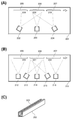
도 1의 (A)에 도시된 적층체(100a)의 에너지 준위에 대하여 도 2의 (A)를 사용하여 설명한다. 적층체(100a)에 사용하는 P형 호스트 및 N형 호스트의 HOMO준위 및 LUMO준위에는 N형 호스트의 HOMO준위<P형 호스트의 HOMO준위<N형 호스트의 LUMO준위<P형 호스트의 LUMO준위라는 관계가 있다.The energy level of the
P형 호스트와 N형 호스트가 혼합된 발광층(102)에서는, 정공은 P형 호스트의 HOMO준위를 이용하여 수송되고, 전자는 N형 호스트의 LUMO준위를 이용하여 수송되기 때문에 캐리어 이동의 관점에서 보면 HOMO준위는 P형 호스트의 HOMO준위, LUMO준위는 N형 호스트의 LUMO준위로 간주할 수 있다. 이 결과, 발광층(102)과 P형 호스트를 포함한 층(103)의 계면에서는 LUMO준위에 갭이 발생하기 때문에 전자의 이동에는 장벽이 된다. 이와 마찬가지로 발광층(102)과 N형 호스트를 포함한 층(104)의 계면에서는 HOMO준위에 갭이 발생하기 때문에 정공의 이동에는 장벽이 된다.In the
한편 발광층(102)과 P형 호스트를 포함한 층(103)의 계면에서는, HOMO준위가 연속적이므로 정공의 이동에는 장벽이 없고, 발광층(102)과 N형 호스트를 포함한 층(104)의 계면에서도 LUMO준위가 연속적이므로 전자의 이동에는 장벽이 없다.On the other hand, at the interface between the light emitting
결과적으로 전자는 N형 호스트를 포함한 층(104)으로부터 발광층(102)으로 이동하기 쉽지만, 발광층(102)과 P형 호스트를 포함한 층(103) 사이에 있는 LUMO준위의 갭에 의하여 발광층(102)으로부터 P형 호스트를 포함한 층(103)으로의 이동은 방해된다.As a result, electrons tend to move from the
이와 마찬가지로 정공은 P형 호스트를 포함한 층(103)으로부터 발광층(102)으로 이동하기 쉽지만, 발광층(102)과 N형 호스트를 포함한 층(104) 사이에 있는 HOMO준위의 갭에 의하여 발광층(102)으로부터 N형 호스트를 포함한 층(104)으로의 이동은 방해된다. 결과적으로 발광층(102)에 전자와 정공을 가둘 수 있다.Likewise, holes easily move from the
도 1의 (B)에 도시된 적층체(100b)의 에너지 준위에 대하여 도 2의 (B)를 사용하여 설명한다. 발광층(102), P형 호스트를 포함한 층(103), 및 N형 호스트를 포함한 층(104)의 HOMO준위 및 LUMO준위는 도 2의 (A)와 마찬가지이다.The energy level of the
상술한 바와 같이 P형 천이 영역(113) 및 N형 천이 영역(114)에서는 P형 호스트의 농도와 N형 호스트의 농도가 연속적으로 변화된다. 그러나 무기 반도체 재료의 전도대나 가전자대가 조성의 변화에 따라 연속적으로 변화하는 경우와는 달리 혼합 유기 화합물의 LUMO준위나 HOMO준위가 연속적으로 변화하는 것은 거의 없다. 이것은 유기 화합물의 전기 전도가 호핑 전도(hopping conduction)란 무기 반도체와는 다른 방식이기 때문이다.As described above, the concentration of the P-type host and the concentration of the N-type host are continuously changed in the P-
예를 들어 N형 호스트의 농도가 저하하고 P형 호스트의 농도가 상승하면 전자는 전도하기 어렵게 되지만, 이것은 LUMO준위가 연속적으로 상승할 뿐만 아니라 N형 호스트 분자끼리의 거리가 길게 되어 이동 확률이 저하하기 때문에 및 근방의 P형 호스트가 높은 LUMO준위에 호핑하기 위한 에너지가 더욱 필요하기 때문이라고 이해된다.For example, if the concentration of the N-type host decreases and the concentration of the P-type host rises, electrons become difficult to conduct, but this not only increases the LUMO level continuously but also increases the distance between the N-type host molecules, thereby decreasing the probability of movement. In this regard, it is understood that the P-type host in the vicinity needs more energy to hop to a high LUMO level.
따라서 N형 천이 영역(114)에서는, 그 HOMO는 N형 호스트의 HOMO와 P형 호스트의 HOMO의 혼합 상태이고, 더 상세하게 말하면 발광층(102)에 가까운 부분에서는 P형 호스트의 HOMO인 확률이 높지만 N형 호스트를 포함한 층(104)에 가까워질 수록 N형 호스트의 HOMO인 확률이 높아진다. P형 천이 영역에서도 마찬가지이다.Therefore, in the N-
그러나 이런 P형 천이 영역(113) 및 N형 천이 영역(114)이 있다고 하더라도, 도 2의 (A)에 도시된 바와 마찬가지로, 발광층(102)과 P형 호스트를 포함한 층(103)의 계면에서는 LUMO준위에 갭이 발생하기 때문에 전자의 이동에는 장벽이 되고, 발광층(102)과 N형 호스트를 포함한 층(104)의 계면에서는 HOMO준위에 갭이 발생하기 때문에 정공의 이동에는 장벽이 된다.However, even if such a P-
다만 도 2의 (A)에 도시된 바와 같이 농도의 변화가 가파르게 되는 계면에서는 예를 들어 전자는 그 계면에 집중적으로 체류하는 확률이 높으므로 계면 부근이 열화되기 쉽다는 문제가 있다. 이에 대하여 도 2의 (B)에 도시된 바와 같이 계면이 애매한 상태에서는 전자가 체류하는 부분은 확률적으로 결정되기 때문에 특정한 부분이 열화되는 일은 없다. 즉 말하자면 발광 소자의 열화를 완화하여 신뢰성을 높일 수 있다.However, as illustrated in FIG. 2A, at the interface where the change in concentration is steep, for example, electrons have a high probability of staying intensively at the interface, and thus there is a problem that the vicinity of the interface is likely to deteriorate. On the other hand, as shown in FIG. 2B, in a state where the interface is ambiguous, the portion where the electron stays is determined probabilisticly, so that the specific portion does not deteriorate. In other words, reliability can be improved by alleviating deterioration of the light emitting device.
한편, 발광층(102)과 P형 천이 영역(113)의 계면 및 P형 천이 영역(113)과 P형 호스트를 포함한 층(103)의 계면에서는 HOMO준위가 연속적이기 때문에 정공의 이동에는 장벽이 없고, 발광층(102)과 N형 천이 영역(114)의 계면 및 N형 천이 영역(114)과 N형 호스트를 포함한 층(104)의 계면에서는 LUMO준위가 연속적이기 때문에 전자의 이동에서는 장벽이 없다.On the other hand, since the HOMO level is continuous at the interface between the light emitting
결과적으로 전자는 N형 호스트를 포함한 층(104)으로부터 발광층(102)으로 이동하기 쉽지만, P형 천이 영역(113)에 있는 LUMO준위의 갭에 의하여 발광층(102)으로부터 P형 호스트를 포함한 층(103)으로의 이동은 방해된다. 이와 마찬가지로 정공은 P형 호스트를 포함한 층(103)으로부터 발광층(102)으로 이동하기 쉽지만 N형 천이 영역(114)에 있는 HOMO준위의 갭에 의하여 발광층(102)으로부터 N형 호스트를 포함한 층(104)으로의 이동은 방해된다.As a result, electrons easily move from the
결과적으로 발광층(102)에 전자와 정공을 가둘 수 있다. 또한 P형 호스트를 포함한 층(103)과 N형 호스트를 포함한 층(104) 사이의 P형 호스트의 농도와 N형 호스트의 농도가 연속적으로 변화하는 적층체(100c)에서도, 상술한 바와 마찬가지로 생각하여 전자와 정공을 P형 호스트를 포함한 층(103)과 N형 호스트를 포함한 층(104) 사이에 효율적으로 가둘 수 있다.As a result, electrons and holes can be trapped in the
다음에 게스트(105)의 발광 과정에 대하여 설명하기로 한다. 여기서는 적층체(100a)를 예로 들어 설명하지만 적층체(100b) 및 적층체(100c)에서도 마찬가지이다. 상술한 바와 같이 인광성 화합물을 게스트로서 사용하는 발광 소자에서의 발광의 일반적인 기본 과정에는 직접 재결합 과정과 에너지 이동 과정이 있다.Next, the light emitting process of the
우선, 도 2의 (C)를 사용하여 직접 재결합 과정에 대하여 설명한다. 양극에 접속된 P형 호스트를 포함한 층(103)으로부터는 정공, 음극에 접속된 N형 호스트를 포함한 층(104)으로부터는 전자가 각각 발광층(102)의 HOMO 및 LUMO에 주입된다. 발광층(102)에는 게스트(105)가 존재하기 때문에, 적절한 조건하에서는 게스트의 HOMO 및 LUMO에 정공 및 전자를 주입하여 게스트를 여기 상태(분자내 여기자, exciton)로 할 수 있다.First, the direct recombination process will be described using FIG. 2C. Holes are injected from the
그러나 발광층(102)에서 군데군데 존재하는 게스트의 HOMO 및 LUMO에 정공 및 전자를 효율적으로 주입하는 것은 기술면에서 보아 어렵기 때문에, 그 과정의 확률은 충분히 높지 않다. 더욱 효율을 높게 하려면 게스트의 LUMO준위를 N형 호스트의 LUMO준위보다 0.1eV~0.3eV 낮게 하여 게스트에 전자를 우선적으로 트랩시키면 좋다. 또한 게스트의 HOMO준위를 P형 호스트의 HOMO준위보다 0.1eV~0.3eV 높게 한 경우에도 같은 효과를 얻을 수 있다. 또한 도 2의 (C)에서는 게스트의 HOMO준위는 P형 호스트의 HOMO준위보다 낮지만 게스트의 LUMO준위는 P형 호스트의 LUMO준위 및 N형 호스트의 LUMO준위보다 충분히 낮으므로 전자는 효율적으로 트랩된다.However, since it is difficult from the technical point of view to efficiently inject holes and electrons into the HOMO and LUMO of the guest existing in several places in the
게스트의 LUMO준위를 N형 호스트의 LUMO준위보다 0.5eV 이상 낮게 하면(또는 게스트의 HOMO준위를 P형 호스트의 HOMO준위보다 0.5eV 이상 높게 하면), 전자(정공)가 트랩되는 확률은 높아지나 발광층(102)의 도전성이 저하하고 또한 음극 측(양극 측)의 게스트만 집중적으로 여기되므로 바람직하지 않다.When the guest's LUMO level is 0.5 eV or more lower than the N-type host's LUMO level (or when the guest's HOMO level is 0.5 eV or more higher than the P-type host's HOMO level), the probability of trapping electrons (holes) increases, but the emission layer is increased. It is not preferable because the conductivity of the 102 decreases and only the guest on the cathode side (anode side) is intensively excited.
다음에 도 2의 (D)를 사용하여 본 발명의 일 형태에 따라 P형 호스트와 N형 호스트를 적절히 선택하고 여기 착체를 형성하는 경우에 대하여 설명한다. 발광층(102)에 상술한 바와 마찬가지로 정공 및 전자가 주입된 경우, 정공 및 전자가 게스트에서 재결합하는 확률보다 발광층(102) 내에서 인접하는 P형 호스트와 N형 호스트에서 재결합하는 확률이 더 높다. 이러한 경우에는 P형 호스트와 N형 호스트는 여기 착체를 형성한다. 여기서 여기 착체에 관하여 상세하게 설명한다.Next, the case where P type host and N type host are appropriately selected according to one embodiment of the present invention and an exciplex is formed using FIG. 2D is described. As described above, when holes and electrons are injected into the
여기 착체는 여기 상태에서의 이종(異種) 분자간의 상호 작용에 의하여 형성된다. 여기 착체는, 비교적 깊은(낮은) LUMO준위를 갖는 재료(여기서는 N형 호스트)와 얕은(높은) HOMO준위를 갖는 재료(여기서는 P형 호스트) 사이에서 형성하기 쉬운 것이 일반적으로 알려져 있다.An exciplex is formed by the interaction between heterogeneous molecules in an excited state. It is generally known that the complex here is easy to form between a material having a relatively deep (low) LUMO level (here N-type host) and a material having a shallow (high) HOMO level (here P-type host).
여기서는, 여기 착체로부터의 발광 파장은 P형 호스트의 HOMO준위와 N형 호스트의 LUMO준위 사이의 에너지 차이에 의존한다. 에너지 차이가 크면 발광 파장은 짧게 되고, 에너지 차이가 작으면 발광 파장은 길게 된다. 그리고, 이 P형 호스트와 N형 호스트에 의하여 여기 착체가 형성된 경우, 여기 착체의 LUMO준위는 N형 호스트에서 유래하고, 여기 착체의 HOMO준위는 P형 호스트에서 유래한다.Here, the emission wavelength from the excitation complex depends on the energy difference between the HOMO level of the P-type host and the LUMO level of the N-type host. If the energy difference is large, the emission wavelength is short, and if the energy difference is small, the emission wavelength is long. When the exciplex is formed by the P-type host and the N-type host, the LUMO level of the exciplex is derived from the N-type host, and the HOMO level of the exciplex is derived from the P-type host.
따라서, 여기 착체의 에너지 차이는 P형 호스트의 에너지 차이나 N형 호스트의 에너지 차이보다 작게 된다. 즉 말하자면, P형 호스트와 N형 호스트 각각의 발광 파장에 비하여 여기 착체의 발광 파장은 긴 파장이 된다.Therefore, the energy difference of the exciplex is smaller than the energy difference of the P-type host or the energy difference of the N-type host. In other words, the emission wavelength of the exciplex is longer than that of each of the P-type host and the N-type host.
여기 착체의 형성 과정은 크게 나누어 이하에서 제시하는 2개의 과정을 생각할 수 있다.The formation process of a complex here can be considered roughly two processes shown below.
《일렉트로플렉스(electroplex)》<< electroplex >>
본 명세서에 있어서, 일렉트로플렉스란, 기저 상태의 P형 호스트 및 기저 상태의 N형 호스트에 의하여 직접 형성된 여기 착체를 가리킨다.In the present specification, the electroplex refers to an exciplex formed directly by the P-type host in the ground state and the N-type host in the ground state.
상술한 바와 같이 일반적인 발광 과정 중의 에너지 이동 과정에서는 정공 및 전자가 호스트 내에서 재결합(여기)하고 여기 상태의 호스트로부터 게스트로 여기 에너지가 이동하여 게스트가 여기 상태에 도달함으로써 발광한다.As described above, in the energy transfer process in the general light emission process, holes and electrons recombine (excitation) in the host, and excitation energy moves from the host in the excited state to the guest, and the guest emits light by reaching the excited state.
여기서 호스트로부터 게스트로 여기 에너지가 이동하기 전에, 호스트 자체가 발광하거나 여기 에너지가 열 에너지가 됨으로써, 여기 에너지가 불활성화된다. 특히, 호스트가 1중항 여기 상태인 경우는 3중항 여기 상태인 경우보다 여기 수명이 짧기 때문에 여기 에너지의 불활성화가 일어나기 쉽다. 이와 같은 여기 에너지의 불활성화는 발광 소자의 열화 및 수명의 저하로 이어지는 요인 중 하나이다.Here, before the excitation energy moves from the host to the guest, the excitation energy is deactivated by the host itself emitting light or the excitation energy becoming thermal energy. In particular, in the case where the host is in the singlet excited state, the excitation life is shorter than in the case of the triplet excited state, so that the excitation energy is easily inactivated. Such deactivation of the excitation energy is one of the factors leading to deterioration of the light emitting device and a decrease in lifespan.
그러나 P형 호스트 및 N형 호스트가 캐리어를 갖는 상태(양이온 또는 음이온)로부터 일렉트로플렉스를 형성하면, 여기 수명이 짧은 1중항 여기자의 형성을 억제할 수 있다. 즉 말하자면 1중항 여기자를 형성하지 않고 직접적으로 여기 착체를 형성하는 과정이 존재할 수 있다. 이에 따라 P형 호스트 또는 N형 호스트의 1중항 여기 에너지의 불활성화도 억제할 수 있다. 따라서 수명이 긴 발광 소자를 실현할 수 있다.However, when the electroplexes are formed from the state where the P-type host and the N-type host have a carrier (cation or anion), the formation of singlet excitons with short excitation life can be suppressed. In other words, there may be a process of forming an exciplex directly without forming singlet excitons. Thereby, inactivation of the singlet excitation energy of a P type host or an N type host can also be suppressed. Therefore, a light emitting element with a long life can be realized.
이로써 본 발명의 일 형태에서는 호스트의 1중항 여기 상태의 발생을 억제하고 이를 대신하여 발생한 일렉트로플렉스로부터 게스트로의 에너지 이동을 하여 발광 효율이 높은 발광 소자를 얻을 수 있다.Thus, in one embodiment of the present invention, the occurrence of the singlet excited state of the host can be suppressed and energy transfer from the generated electroplex to the guest can be obtained, thereby obtaining a light emitting device having high luminous efficiency.
《여기자에 의한 여기 착체의 형성》<< formation of exciplex by exciter >>
또 하나의 과정으로서는, P형 호스트 또는 N형 호스트 중 한쪽이 1중항 여기자를 형성한 후, 기저 상태의 다른 쪽과 상호 작용하여 여기 착체를 형성하는 기본 과정을 생각할 수 있다. 일렉트로플렉스와는 달리, 이 경우에는 일단 P형 호스트 또는 N형 호스트의 1중항 여기 상태가 생성되지만 이것은 신속히 여기 착체로 변환되기 때문에 1중항 여기 에너지의 불활성화를 억제할 수 있다. 따라서 호스트의 여기 에너지의 불활성화를 억제할 수 있다.As another process, one of the P-type host and the N-type host may form a singlet exciton, and then a basic process of interacting with the other in the ground state to form an exciplex. Unlike the electroplex, in this case, the singlet excited state of the P-type host or the N-type host is generated once, but since it is rapidly converted into the exciplex, the inactivation of the singlet excitation energy can be suppressed. Therefore, inactivation of the excitation energy of the host can be suppressed.
또한 P형 호스트와 N형 호스트의 HOMO준위의 차이, 및 LUMO준위의 차이가 큰 경우(구체적으로는 차이가 0.3eV 이상), 전자는 우선적으로 N형 호스트에 들어가고, 정공은 우선적으로 P형 호스트에 들어간다. 이 경우, 1중항 여기자를 거쳐 여기 착체가 형성되는 과정보다 일렉트로플렉스가 형성되는 과정이 일어나기 쉽다고 생각된다.In addition, when the difference between the HOMO level and the LUMO level between the P-type host and the N-type host is large (specifically, 0.3 eV or more), the electrons enter the N-type host first, and the holes preferentially enter the P-type host. Enter In this case, it is considered that the process of forming the electroflex is more likely to occur than the process of forming the exciplex through the singlet excitons.
또한 에너지 이동 과정의 효율을 높이기 위해서는, 푀르스터 기구 및 덱스터 기구 중 어느 경우에도 MLCT 천이에서 유래하는 흡수대의 중요성을 고려하면 P형 호스트(또는 N형 호스트) 단독의 발광 스펙트럼과 게스트의 흡수 스펙트럼의 중첩보다 여기 착체의 발광 스펙트럼과 게스트의 흡수 스펙트럼의 중첩을 크게 하는 것이 바람직하다.In addition, in order to increase the efficiency of the energy transfer process, in consideration of the importance of the absorption band derived from the MLCT transition in either of the wormster mechanism and the dexter mechanism, the emission spectrum of the P-type host (or N-type host) alone and the absorption spectrum of the guest It is preferable to make the superposition of the emission spectrum of an exciplex and the absorption spectrum of a guest larger than superposition.
또한 에너지 이동의 효율을 높이기 위해서는, 농도 소광이 일어나지 않을 정도로 게스트의 농도를 높이는 것이 바람직하고, P형 호스트와 N형 호스트의 총량에 대한 게스트의 농도는 중량비로 1%~9%로 하면 바람직하다.In addition, in order to increase the efficiency of energy transfer, it is preferable to increase the concentration of the guest so that concentration quenching does not occur, and the concentration of the guest with respect to the total amount of the P-type host and the N-type host is preferably 1% to 9% by weight. .
본 실시형태에서는, P형 호스트 및 N형 호스트 내에 존재하는 게스트를 P형 호스트와 N형 호스트의 여기 착체로부터의 에너지 이동에 의하여 여기 상태로 하는 개념을 이용함으로써, 캐리어의 가둠과 발광층으로의 캐리어 주입 장벽의 저감이 동시에 달성될 뿐만 아니라 여기 착체를 형성하고 그 1중항 여기 상태와 3중항 여기 상태 쌍방으로부터의 에너지 이동 과정을 이용할 수 있으므로, 효율이 높으며 저전압 구동의(즉 말하자면 파워 효율이 매우 높은) 발광 소자를 얻을 수 있다.In this embodiment, the confinement of the carrier and the carrier to the light emitting layer are made possible by utilizing the concept that the guest existing in the P-type host and the N-type host is excited by the energy transfer from the excitation complex of the P-type host and the N-type host. Not only is the reduction of the injection barrier achieved at the same time, but also the formation of an exciplex and the use of energy transfer processes from both the singlet and triplet excited states, resulting in high efficiency and low voltage drive (i.e. very high power efficiency). ) A light emitting device can be obtained.
<게스트><Guest>
게스트에는 인광성 화합물을 사용할 수 있고 유기 금속 착체가 바람직하고 유기 금속 이리듐 착체가 특히 바람직하다. 또한 푀르스터 기구에 의한 에너지 이동을 고려하면 인광성 화합물의 가장 긴 파장 측에 위치하는 흡수대의 mol흡광계수는 2000M-1·cm-1 이상이 바람직하고 5000M-1·cm-1 이상이 특히 바람직하다.Phosphorescent compounds can be used for the guest, and organometallic complexes are preferred, and organometallic iridium complexes are particularly preferred. Also, phosphorescent mol extinction coefficient at the absorption band located at the longest wavelength side of the compound is 2000M -1 · cm or more is preferable, and 5000M -1 · cm -1 or more, particularly preferably -1 considering the energy transfer mechanism by the requester poereu Do.
상술한 바와 같이 큰 mol흡광계수를 갖는 화합물로서는 예를 들어 비스(3,5-다이메틸-2-페닐피라지나토)(다이피발로일메타나토)이리듐(Ⅲ)(약칭: [Ir(mppr-Me)2(dpm)])이나 (아세틸아세토나토)비스(4,6-다이페닐피리미디나토)이리듐(Ⅲ)(약칭: [Ir(dppm)2(acac)]) 등을 들 수 있다. 특히 [Ir(dppm)2(acac)]와 같이 mol흡광계수가 5000M-1·cm-1 이상에 달하는 재료를 사용하면 외부 양자 효율이 30% 정도에 달하는 발광 소자를 얻을 수 있다.As the compound having a large mol extinction coefficient as described above, for example, bis (3,5-dimethyl-2-phenylpyrazinato) (dipivaloylmethanato) iridium (III) (abbreviated as: [Ir (mppr) -Me) 2 (dpm)]) and (acetylacetonato) bis (4,6-diphenylpyrimidinato) iridium (III) (abbreviated as [Ir (dppm) 2 (acac)]). . In particular, when a material having a mol absorption coefficient of 5000M −1 · cm −1 or more, such as [Ir (dppm) 2 (acac)], is used, a light emitting device having an external quantum efficiency of about 30% can be obtained.
게스트에 사용할 수 있는 인광성 화합물에 대하여 상술한 것 이외의 예를 든다. 예를 들어 440nm~520nm에 발광 피크를 갖는 인광성 화합물로서는, 트리스{2-[5-(2-메틸페닐)-4-(2,6-다이메틸페닐)-4H-1,2,4-트라이아졸-3-일-κN2]페닐-κC}이리듐(Ⅲ)(약칭: [Ir(mpptz-dmp)3]), 트리스(5-메틸-3,4-다이페닐-4H-1,2,4-트라이아졸라토)이리듐(Ⅲ)(약칭: [Ir(Mptz)3]), 트리스[4-(3-바이페닐)-5-이소프로필-3-페닐-4H-1,2,4-트라이아졸라토]이리듐(Ⅲ)(약칭: [Ir(iPrptz-3b)3])과 같은 4H-트라이아졸 골격을 갖는 유기 금속 이리듐 착체나, 트리스[3-메틸-1-(2-메틸페닐)-5-페닐-1H-1,2,4-트라이아졸라토]이리듐(Ⅲ)(약칭: [Ir(Mptz1-mp)3]), 트리스(1-메틸-5-페닐-3-프로필-1H-1,2,4-트라이아졸라토)이리듐(Ⅲ)(약칭: [Ir(Prptz1-Me)3])과 같은 1H-트라이아졸 골격을 갖는 유기 금속 이리듐 착체나, fac-트리스[1-(2,6-다이이소프로필페닐)-2-페닐-1H-이미다졸]이리듐(Ⅲ)(약칭: [Ir(iPrpmi)3]), 트리스[3-(2,6-다이메틸페닐)-7-메틸이미다조[1,2-f]페난트리디나토]이리듐(Ⅲ)(약칭: [Ir(dmpimpt-Me)3])과 같은 이미다졸 골격을 갖는 유기 금속 이리듐 착체나, 비스[2-(4',6'-다이플루오로페닐)피리디나토-N,C2']이리듐(Ⅲ)테트라키스(1-피라졸릴)보레이트(약칭: FIr6), 비스[2-(4',6'-다이플루오로페닐)피리디나토-N,C2']이리듐(Ⅲ)피콜리네이트(약칭:FIrpic), 비스{2-[3',5'-비스(트라이플루오로메틸)페닐]피리디나토-N,C2'}이리듐(Ⅲ)피콜리네이트(약칭: [Ir(CF3ppy)2(pic)]), 비스[2-(4',6'-다이플루오로페닐)피리디나토-N,C2']이리듐(Ⅲ)아세틸아세토네이트(약칭: FIracac)와 같은 전자 흡인기를 갖는 페닐피리딘 유도체를 배위자로 하는 유기 금속 이리듐 착체를 들 수 있다. 상술한 것 중에서도 4H-트라이아졸 골격을 갖는 유기 금속 이리듐 착체는 신뢰성이나 발광 효율이 우수하기 때문에 특히 바람직하다.Examples of the phosphorescent compound that can be used for the guest are given. For example, as a phosphorescent compound having an emission peak at 440 nm to 520 nm, tris {2- [5- (2-methylphenyl) -4- (2,6-dimethylphenyl) -4H-1,2,4-triazole -3-yl-κN 2 ] phenyl-κC} iridium (III) (abbreviated as [Ir (mpptz-dmp) 3 ]), tris (5-methyl-3,4-diphenyl-4H-1,2,4 Triazolato) iridium (III) (abbreviated as [Ir (Mptz) 3 ]), tris [4- (3-biphenyl) -5-isopropyl-3-phenyl-4H-1,2,4-tri Triazol- 3 -yl) azolate] iridium (III) (abbreviation: [Ir (iPrptz-3b) 3 ]) or an organic metal iridium complex having a 4H- -Phenyl-1H-1,2,4-triazolato] iridium (III) (abbreviated: [Ir (Mptz1-mp) 3 ]), tris (1-methyl-5-phenyl-3-propyl-1H-1 Organometallic iridium complexes having a 1H-triazole skeleton such as 2,4-triazolato) iridium (III) (abbreviated as [Ir (Prptz1-Me) 3 ]), or fac-tris [1- (2, 6-diisopropylphenyl) -2-phenyl-1H-imidazole] iridium (III) (abbreviated as [Ir (iPrpmi) 3 ]), tris [3- (2,6 Organometallic iridium with an imidazole skeleton such as -dimethylphenyl) -7-methylimidazo [1,2-f] phenantridinato] iridium (III) (abbreviated: [Ir (dmpimpt-Me) 3 ]) or complex, bis [2- (4 ', 6'-difluorophenyl) pyrimidin Dina sat -N, C 2'] iridium (ⅲ) tetrakis (1-pyrazolyl) borate (abbreviation: FIr6), bis [ 2- (4 ', 6'-difluorophenyl) pyridinato-N, C 2' ] iridium (III) picolinate (abbreviation: Firpic), bis {2- [3 ', 5'-bis ( Trifluoromethyl) phenyl] pyridinato-N, C 2 ' } iridium (III) picolinate (abbreviated: [Ir (CF 3 ppy) 2 (pic)]), bis [2- (4', 6 Organometallic iridium complexes having a phenylpyridine derivative having an electron withdrawing group such as '-difluorophenyl) pyridinato-N, C 2' ] iridium (III) acetylacetonate (abbreviated as FIracac) as a ligand . Among the above-mentioned, the organometallic iridium complex which has a 4H-triazole skeleton is especially preferable because it is excellent in reliability and luminous efficiency.
또한, 예를 들어 520nm~600nm에 발광 피크를 갖는 인광성 화합물로서는, 트리스(4-메틸-6-페닐피리미디나토)이리듐(Ⅲ)(약칭: [Ir(mppm)3]), 트리스(4-t-부틸-6-페닐피리미디나토)이리듐(Ⅲ)(약칭: [Ir(tBuppm)3]), (아세틸아세토나토)비스(6-메틸-4-페닐피리미디나토)이리듐(Ⅲ)(약칭: [Ir(mppm)2(acac)]), (아세틸아세토나토)비스(6-tert-부틸-4-페닐피리미디나토)이리듐(Ⅲ)(약칭: [Ir(tBuppm)2(acac)]), (아세틸아세토나토)비스[4-(2-노르보르닐)-6-페닐피리미디나토]이리듐(Ⅲ)(endo-,exo-혼합물)(약칭: [Ir(nbppm)2(acac)]), (아세틸아세토나토)비스[5-메틸-6-(2-메틸페닐)-4-페닐피리미디나토]이리듐(Ⅲ)(약칭: [Ir(mpmppm)2(acac)])과 같은 피리미딘 골격을 갖는 유기 금속 이리듐 착체나, (아세틸아세토나토)비스(3,5-다이메틸-2-페닐피라지나토)이리듐(Ⅲ)(약칭: [Ir(mppr-Me)2(acac)]), (아세틸아세토나토)비스(5-이소프로필-3-메틸-2-페닐피라지나토)이리듐(Ⅲ)(약칭: [Ir(mppr-iPr)2(acac)])과 같은 피라진 골격을 갖는 유기 금속 이리듐 착체나, 트리스(2-페닐피리디나토-N,C2')이리듐(Ⅲ)(약칭: [Ir(ppy)3]), 비스(2-페닐피리디나토-N,C2')이리듐(Ⅲ)아세틸아세토네이트(약칭: [Ir(ppy)2(acac)]), 비스(벤조[h]퀴놀리나토)이리듐(Ⅲ)아세틸아세토네이트(약칭: [Ir(bzq)2(acac)]), 트리스(벤조[h]퀴놀리나토)이리듐(Ⅲ)(약칭: [Ir(bzq)3]), 트리스(2-페닐퀴놀리나토-N,C2')이리듐(Ⅲ)(약칭: [Ir(pq)3]), 비스(2-페닐퀴놀리나토-N,C2')이리듐(Ⅲ)아세틸아세토네이트(약칭: [Ir(pq)2(acac)])와 같은 피리딘 골격을 갖는 유기 금속 이리듐 착체 외에, 트리스(아세틸아세토나토)(모노페난트롤린)테르븀(Ⅲ)(약칭: [Tb(acac)3(Phen)])과 같은 희토류 금속 착체를 들 수 있다. 상술한 것 중에서도 피리미딘 골격을 갖는 유기 금속 이리듐 착체는 신뢰성이나 발광 효율이 매우 우수하기 때문에 특히 바람직하다.For example, as a phosphorescent compound having an emission peak at 520 nm to 600 nm, tris (4-methyl-6-phenylpyrimidinato) iridium (III) (abbreviated as [Ir (mppm) 3 ]) and tris (4) t -butyl-6-phenylpyrimidinato) iridium (III) (abbreviated as [Ir (tBuppm) 3 ]), (acetylacetonato) bis (6-methyl-4-phenylpyrimidinato) iridium (III) (abbreviation: [Ir (mppm) 2 ( acac)]), ( acetylacetonato) bis (6- tert - butyl-4-phenyl-pyrimidinyl NATO) iridium (ⅲ) (abbreviation: [Ir (tBuppm) 2 ( acac )]), (Acetylacetonato) bis [4- (2-norbornyl) -6-phenylpyrimidinato] iridium (III) (endo-, exo-mixture) (abbreviated as: [Ir (nbppm) 2 ( acac)]), (acetylacetonato) bis [5-methyl-6- (2-methylphenyl) -4-phenylpyrimidinato] iridium (III) (abbreviated as [Ir (mpmppm) 2 (acac)]) and Organometallic iridium complexes having the same pyrimidine backbone or (acetylacetonato) bis (3,5-dimethyl-2-phenylpyrazinato) iridium (III) (abbreviated as: [Ir (mppr-Me) 2 (acac) )]), (Acetyl Seto NATO) bis (5-isopropyl-3-methyl-2-phenyl-pyrazol through Saturday) iridium (Ⅲ) (abbreviation: [Ir (mppr-iPr) 2 (acac)] The organometallic iridium having a pyrazine skeleton, such as a) Complex or tris (2-phenylpyridinato-N, C 2 ′ ) iridium (III) (abbreviated as [Ir (ppy) 3 ]), bis (2-phenylpyridinato-N, C 2 ′ ) iridium (III) acetylacetonate (abbreviation: [Ir (ppy) 2 (acac)]), bis (benzo [h] quinolinato) iridium (III) acetylacetonate (abbreviation: [Ir (bzq) 2 (acac)) ]), tris (benzo [h] quinolinato) iridium (ⅲ) (abbreviation: [Ir (bzq) 3]), tris (2-phenyl-quinolinato -N, C 2 ') iridium (ⅲ) (abbreviated : [Ir (pq) 3] ), bis (2-phenyl-quinolinato -N, C 2 ') iridium (ⅲ) acetylacetonate (abbreviation: pyridine skeleton, such as [Ir (pq) 2 (acac )]) In addition to the organometallic iridium complex having, a rare earth metal complex such as tris (acetylacetonato) (monophenanthroline) terbium (III) (abbreviated as [Tb (acac) 3 (Phen)]) is mentioned. Among the above-mentioned, the organometallic iridium complex which has a pyrimidine skeleton is especially preferable because it is very excellent in reliability and luminous efficiency.
또한, 예를 들어 600nm~700nm에 발광 피크를 갖는 인광성 화합물로서는, (다이이소부티릴메타나토)비스[4,6-비스(3-메틸페닐)피리미디나토]이리듐(Ⅲ)(약칭: [Ir(5mdppm)2(dibm)]), 비스[4,6-비스(3-메틸페닐)피리미디나토](다이피발로일메타나토)이리듐(Ⅲ)(약칭: [Ir(5mdppm)2(dpm)]), 비스[4,6-다이(나프탈렌-1-일)피리미디나토](다이피발로일메타나토)이리듐(Ⅲ)(약칭: [Ir(d1npm)2(dpm)])과 같은 피리미딘 골격을 갖는 유기 금속 이리듐 착체나, (아세틸아세토나토)비스(2,3,5-트라이페닐피라지나토)이리듐(Ⅲ)(약칭: [Ir(tppr)2(acac)]), 비스(2,3,5-트라이페닐피라지나토)(다이피발로일메타나토)이리듐(Ⅲ)(약칭: [Ir(tppr)2(dpm)]), (아세틸아세토나토)비스[2,3-비스(4-플루오로페닐)퀴녹살리나토]이리듐(Ⅲ)(약칭: [Ir(Fdpq)2(acac)])과 같은 피라진 골격을 갖는 유기 금속 이리듐 착체나, 트리스(1-페닐이소퀴놀리나토-N,C2')이리듐(Ⅲ)(약칭: [Ir(piq)3]), 비스(1-페닐이소퀴놀리나토-N,C2')이리듐(Ⅲ)아세틸아세토네이트(약칭: [Ir(piq)2(acac)])와 같은 피리딘 골격을 갖는 유기 금속 이리듐 착체 외에 2,3,7,8,12,13,17,18-옥타에틸-21H,23H-포르피린백금(Ⅱ)(약칭: PtOEP)과 같은 백금 착체나, 트리스(1,3-다이페닐-1,3-프로판디오나토)(모노페난트롤린)유로퓸(Ⅲ)(약칭: [Eu(DBM)3(Phen)]), 트리스[1-(2-테노일)-3,3,3-트라이플루오로아세토나토](모노페난트롤린)유로퓸(Ⅲ)(약칭: [Eu(TTA)3(Phen)])과 같은 희토류 금속 착체를 들 수 있다. 상술한 것 중에서도 피리미딘 골격을 갖는 유기 금속 이리듐 착체는 신뢰성이나 발광 효율이 매우 우수하기 때문에 특히 바람직하다. 또한, 피라진 골격을 갖는 유기 금속 이리듐 착체는 색도가 좋은 적색 발광이 얻어진다.For example, as a phosphorescent compound having an emission peak at 600 nm to 700 nm, (diisobutyrylmethanato) bis [4,6-bis (3-methylphenyl) pyrimidinato] iridium (III) (abbreviated as: [ Ir (5mdppm) 2 (dibm)]), bis [4,6-bis (3-methylphenyl) pyrimidinato] (dipivaloylmethanato) iridium (III) (abbreviated: [Ir (5mdppm) 2 (dpm) )]), Such as bis [4,6-di (naphthalen-1-yl) pyrimidinato] (dipivaloylmethanato) iridium (III) (abbreviated: [Ir (d1npm) 2 (dpm)]) Organometallic iridium complex having a pyrimidine skeleton, (acetylacetonato) bis (2,3,5-triphenylpyrazinato) iridium (III) (abbreviated as [Ir (tppr) 2 (acac)]), bis (2,3,5-triphenylpyrazinato) (dipivaloylmethanato) iridium (III) (abbreviated as [Ir (tppr) 2 (dpm)]), (acetylacetonato) bis [2,3 Organometallic iridium complexes having a pyrazine skeleton such as -bis (4-fluorophenyl) quinoxalanato] iridium (III) (abbreviated as [Ir (Fdpq) 2 (acac)]); Lis (1-phenylisoquinolinato-N, C 2 ' ) iridium (III) (abbreviated as [Ir (piq) 3 ]), bis (1-phenylisoquinolinato-N, C 2' ) iridium ( III) acetylacetonate (abbreviated: 2,3,7,8,12,13,17,18-octaethyl-21H in addition to an organometallic iridium complex having a pyridine skeleton such as [Ir (piq) 2 (acac)]) Platinum complexes such as 23H-porphyrin platinum (II) (abbreviated as PtOEP) or tris (1,3-diphenyl-1,3-propanedioato) (monophenanthroline) europium (III) (abbreviated as: Eu (DBM) 3 (Phen)]), tris [1- (2-tenoyl) -3,3,3-trifluoroacetonato] (monophenanthroline) europium (III) (abbreviated as: [Eu ( And rare earth metal complexes such as TTA) 3 (Phen)]). Among the above-mentioned, the organometallic iridium complex which has a pyrimidine skeleton is especially preferable because it is very excellent in reliability and luminous efficiency. In addition, the iridium complex of the organometallic having the pyrazine skeleton can obtain red luminescence with good chromaticity.
<P형 호스트><P-type host>
P형 호스트는 정공 수송성의 유기 화합물이다. 이런 유기 화합물로서는 π전자 과잉형 복소 방향족 화합물(예를 들어 카바졸 유도체나 인돌 유도체)이나 방향족 아민 화합물을 적합하게 사용할 수 있고, 예를 들어 4-페닐-4'-(9-페닐-9H-카바졸-3-일)트라이페닐아민(약칭: PCBA1BP), 4,4'-다이(1-나프틸)-4''-(9-페닐-9H-카바졸-3-일)트라이페닐아민(약칭: PCBNBB), 4,4'-비스[N-(1-나프틸)-N-페닐아미노]바이페닐(약칭: NPB 또는 α-NPD), 3-[N-(1-나프틸)-N-(9-페닐카바졸-3-일)아미노]-9-페닐카바졸(약칭: PCzPCN1), 4,4',4''-트리스[N-(1-나프틸)-N-페닐아미노]트라이페닐아민(약칭: 1'-TNATA), 2,7-비스[N-(4-다이페닐아미노페닐)-N-페닐아미노]-스피로-9,9'-바이플루오렌(약칭: DPA2SF), N,N'-비스(9-페닐카바졸-3-일)-N,N'-다이페닐벤젠-1,3-다이아민(약칭: PCA2B), N-(9,9-다이메틸-2-다이페닐아미노-9H-플루오렌-7-일)다이페닐아민(약칭: DPNF), N,N',N''-트라이페닐-N,N',N''-트리스(9-페닐카바졸-3-일)벤젠-1,3,5-트라이아민(약칭: PCA3B), 2-[N-(9-페닐카바졸-3-일)-N-페닐아미노]스피로-9,9'-바이플루오렌(약칭: PCASF), 2-[N-(4-다이페닐아미노페닐)-N-페닐아미노]스피로-9,9'-바이플루오렌(약칭: DPASF), N,N'-비스[4-(카바졸-9-일)페닐]-N,N'-다이페닐-9,9-다이메틸플루오렌-2,7-다이아민(약칭: YGA2F), N,N'-비스(3-메틸페닐)-N,N'-다이페닐-[1,1'-바이페닐]-4,4'-다이아민(약칭: TPD), 4,4'-비스[N-(4-다이페닐아미노페닐)-N-페닐아미노]바이페닐(약칭: DPAB), N-(9,9-다이메틸-9H-플루오렌-2-일)-N-{9,9-다이메틸-2-[N'-페닐-N'-(9,9-다이메틸-9H-플루오렌-2-일)아미노]-9H-플루오렌-7-일}-페닐아민(약칭: DFLADFL), 3-[N-(9-페닐카바졸-3-일)-N-페닐아미노]-9-페닐카바졸(약칭: PCzPCA1), 3-[N-(4-다이페닐아미노페닐)-N-페닐아미노]-9-페닐카바졸(약칭: PCzDPA1), 3,6-비스[N-(4-다이페닐아미노페닐)-N-페닐아미노]-9-페닐카바졸(약칭: PCzDPA2), 4,4'-비스(N-{4-[N'-(3-메틸페닐)-N'-페닐아미노]페닐}-N-페닐아미노)바이페닐(약칭: DNTPD), 3,6-비스[N-(4-다이페닐아미노페닐)-N-(1-나프틸)아미노]-9-페닐카바졸(약칭: PCzTPN2), 3,6-비스[N-(9-페닐카바졸-3-일)-N-페닐아미노]-9-페닐카바졸(약칭: PCzPCA2) 등을 들 수 있다.P type hosts are hole transporting organic compounds. As such an organic compound, (pi) electron excess type hetero aromatic compound (for example, a carbazole derivative or an indole derivative) and an aromatic amine compound can be used suitably, For example, 4-phenyl-4 '-(9-phenyl-9H- Carbazol-3-yl) triphenylamine (abbreviated: PCBA1BP), 4,4'-di (1-naphthyl) -4 ''-(9-phenyl-9H-carbazol-3-yl) triphenylamine (Abbreviated: PCBNBB), 4,4'-bis [N- (1-naphthyl) -N-phenylamino] biphenyl (abbreviated: NPB or α-NPD), 3- [N- (1-naphthyl) -N- (9-phenylcarbazol-3-yl) amino] -9-phenylcarbazole (abbreviated: PCzPCN1), 4,4 ', 4' '-tris [N- (1-naphthyl) -N- Phenylamino] triphenylamine (abbreviated: 1'-TNATA), 2,7-bis [N- (4-diphenylaminophenyl) -N-phenylamino] -spiro-9,9'-bifluorene (abbreviated) : DPA2SF), N, N'-bis (9-phenylcarbazol-3-yl) -N, N'-diphenylbenzene-1,3-diamine (abbreviated as: PCA2B), N- (9,9- Dimethyl-2-diphenylamino-9H-fluoren-7-yl) diphenylamine (abbreviated: DPNF), N, N ', N' '-tri Nyl-N, N ', N' '-tris (9-phenylcarbazol-3-yl) benzene-1,3,5-triamine (abbreviated: PCA3B), 2- [N- (9-phenylcarbazole -3-yl) -N-phenylamino] spiro-9,9'-bifluorene (abbreviated as: PCASF), 2- [N- (4-diphenylaminophenyl) -N-phenylamino] spiro-9, 9'-bifluorene (abbreviated: DPASF), N, N'-bis [4- (carbazol-9-yl) phenyl] -N, N'-diphenyl-9,9-dimethylfluorene-2 , 7-diamine (abbreviated: YGA2F), N, N'-bis (3-methylphenyl) -N, N'-diphenyl- [1,1'-biphenyl] -4,4'-diamine (abbreviated) : TPD), 4,4'-bis [N- (4-diphenylaminophenyl) -N-phenylamino] biphenyl (abbreviated as: DPAB), N- (9,9-dimethyl-9H-fluorene- 2-yl) -N- {9,9-dimethyl-2- [N'-phenyl-N '-(9,9-dimethyl-9H-fluoren-2-yl) amino] -9H-fluorene -7-yl} -phenylamine (abbreviated: DFLADFL), 3- [N- (9-phenylcarbazol-3-yl) -N-phenylamino] -9-phenylcarbazole (abbreviated: PCzPCA1), 3- [N- (4-diphenylaminophenyl) -N-phenylamino] -9-phenylcarbazole (abbreviated as: PCzDPA1), 3,6-bis [N- (4-diphenyla Nophenyl) -N-phenylamino] -9-phenylcarbazole (abbreviated: PCzDPA2), 4,4'-bis (N- {4- [N '-(3-methylphenyl) -N'-phenylamino] phenyl } -N-phenylamino) biphenyl (abbreviated as DNTPD), 3,6-bis [N- (4-diphenylaminophenyl) -N- (1-naphthyl) amino] -9-phenylcarbazole (abbreviated as: : PCzTPN2), 3,6-bis [N- (9-phenylcarbazol-3-yl) -N-phenylamino] -9-phenylcarbazole (abbreviated as: PCzPCA2), etc. are mentioned.
<N형 호스트><N-type host>
N형 호스트는 전자 수송성의 유기 화합물이다. 이런 유기 화합물로서는 질소 함유 복소 방향족 화합물과 같은 π전자 부족형 복소 방향족 화합물이나 퀴놀린 골격 또는 벤조퀴놀린 골격을 갖는 금속 착체, 옥사졸계 배위자 또는 티아졸계 배위자를 갖는 금속 착체 등을 사용할 수 있다.N-type host is an electron transporting organic compound. As such organic compounds,? -Electron deficient heteroaromatic compounds such as nitrogen-containing heteroaromatic compounds, metal complexes having a quinoline skeleton or a benzoquinoline skeleton, an oxazole ligand or a metal complex having a thiazole ligand may be used.
구체적으로는 비스(10-하이드록시벤조[h]퀴놀리나토)베릴륨(Ⅱ)(약칭: BeBq2), 비스(2-메틸-8-퀴놀리놀라토)(4-페닐페놀라토)알루미늄(Ⅲ)(약칭: BAlq), 비스(8-퀴놀리놀라토)아연(Ⅱ)(약칭: Znq), 비스[2-(2-벤조옥사졸릴)페놀라토)아연(Ⅱ)(약칭: Zn(BOX)2), 비스[2-(2-벤조티아졸릴)페놀라토]아연(Ⅱ)(약칭: Zn(BTZ)2) 등의 금속 착체, 2-(4-바이페니릴)-5-(4-tert-부틸페닐)-1,3,4-옥사다이아졸(약칭: PBD), 3-(4-바이페니릴)-4-페닐-5-(4-tert-부틸페닐)-1,2,4-트라이아졸(약칭: TAZ), 1,3-비스[5-(p-tert-부틸페닐)-1,3,4-옥사다이아졸-2-일]벤젠(약칭: OXD-7), 9-[4-(5-페닐-1,3,4-옥사다이아졸-2-일)페닐]-9H-카바졸(약칭: CO11), 2,2',2''-(1,3,5-벤젠트라이일)트리스(1-페닐-1H-벤조이미다졸)(약칭: TPBI), 2-[3-(다이벤조티오펜-4-일)페닐]-1-페닐-1H-벤조이미다졸(약칭: mDBTBIm-Ⅱ) 등의 폴리아졸 골격을 갖는 복소 고리 화합물, 2-[3-(다이벤조티오펜-4-일)페닐]다이벤조[f,h]퀴녹살린(약칭: 2mDBTPDBq-Ⅱ), 7-[3-(다이벤조티오펜-4-일)페닐]다이벤조[f,h]퀴녹살린(약칭: 7mDBTPDBq-Ⅱ), 6-[3-(다이벤조티오펜-4-일)페닐]다이벤조[f,h]퀴녹살린(약칭: 6mDBTPDBq-Ⅱ), 2-[3'-(다이벤조티오펜-4-일)바이페닐-3-일]다이벤조[f,h]퀴녹살린(약칭: 2mDBTBPDBq-Ⅱ), 2-[4-(다이벤조티오펜-4-일)페닐]다이벤조[f,h]퀴녹살린(약칭: 2DBTPDBq-Ⅱ), 2-[4-(3,6-다이페닐-9H-카바졸-9-일)페닐]다이벤조[f,h]퀴녹살린(약칭: 2CzPDBq-Ⅲ), 2-[3'-(9H-카바졸-9-일)바이페닐-3-일]다이벤조[f,h]퀴녹살린(약칭: 2mCzBPDBq) 등의 퀴녹살린 골격 또는 다이벤조퀴녹살린 골격을 갖는 복소 고리 화합물, 4,6-비스[3-(페난트렌-9-일)페닐]피리미딘(약칭: 4,6mPnP2Pm), 4,6-비스[3-(9H-카바졸-9-일)페닐]피리미딘(약칭: 4,6mCzP2Pm), 4,6-비스[3-(4-다이벤조티에닐)페닐]피리미딘(약칭: 4,6mDBTP2Pm-Ⅱ) 등의 다이아진 골격(피리미딘 골격이나 피라진 골격)을 갖는 복소 고리 화합물, 3,5-비스[3-(9H-카바졸-9-일)페닐]피리딘(약칭: 35DCzPPy), 1,3,5-트라이[3-(3-피리딜)페닐]벤젠(약칭: TmPyPB), 3,3',5,5'-테트라[(m-피리딜)-펜-3-일]바이페닐(약칭: BP4mPy) 등의 피리딘 골격을 갖는 복소 고리 화합물을 들 수 있다. 상술한 것 중에서도 퀴녹살린 골격 또는 다이벤조퀴녹살린 골격을 갖는 복소 고리 화합물, 다이아진 골격을 갖는 복소 고리 화합물, 피리딘 골격을 갖는 복소 고리 화합물은 신뢰성이 양호하여 바람직하다.Specifically, bis (10-hydroxybenzo [h] quinolinato) beryllium (II) (abbreviated: BeBq 2 ), bis (2-methyl-8-quinolinolato) (4-phenylphenolato) aluminum ( III) (abbreviated: BAlq), bis (8-quinolinolato) zinc (II) (abbreviated: Znq), bis [2- (2-benzooxazolyl) phenololato) zinc (II) (abbreviated: Zn ( BOX) 2 ), metal complexes such as bis [2- (2-benzothiazolyl) phenolato] zinc (II) (abbreviated as Zn (BTZ) 2 ), 2- (4-biphenylyl) -5- ( 4- tert -butylphenyl) -1,3,4-oxadiazole (abbreviated as PBD), 3- (4-biphenyryl) -4-phenyl-5- (4- tert -butylphenyl) -1, 2,4-triazole (abbreviated: TAZ), 1,3-bis [5- (p- tert -butylphenyl) -1,3,4-oxadiazol-2-yl] benzene (abbreviated: OXD-7 ), 9- [4- (5-phenyl-1,3,4-oxadiazol-2-yl) phenyl] -9H-carbazole (abbreviated as: CO11), 2,2 ', 2''-(1 , 3,5-benzenetriyl) tris (1-phenyl-1H-benzoimidazole) (abbreviated: TPBI), 2- [3- (dibenzothiophen-4-yl) phenyl] -1-phenyl-1H -Having a polyazole skeleton such as benzoimidazole (abbreviated name: mDBTBIm-II) Minor ring compound, 2- [3- (dibenzothiophen-4-yl) phenyl] dibenzo [f, h] quinoxaline (abbreviated: 2mDBTPDBq-II), 7- [3- (dibenzothiophen-4 -Yl) phenyl] dibenzo [f, h] quinoxaline (abbreviated: 7mDBTPDBq-II), 6- [3- (dibenzothiophen-4-yl) phenyl] dibenzo [f, h] quinoxaline (abbreviated) : 6mDBTPDBq-II), 2- [3 '-(dibenzothiophen-4-yl) biphenyl-3-yl] dibenzo [f, h] quinoxaline (abbreviated: 2mDBTBPDBq-II), 2- [4 -(Dibenzothiophen-4-yl) phenyl] dibenzo [f, h] quinoxaline (abbreviated: 2DBTPDBq-II), 2- [4- (3,6-diphenyl-9H-carbazole-9- Yl) phenyl] dibenzo [f, h] quinoxaline (abbreviated: 2CzPDBq-III), 2- [3 '-(9H-carbazol-9-yl) biphenyl-3-yl] dibenzo [f, h Heterocyclic compound having a quinoxaline skeleton or a dibenzoquinoxaline skeleton, such as] quinoxaline (abbreviation: 2mCzBPDBq), 4,6-bis [3- (phenanthrene-9-yl) phenyl] pyrimidine (abbreviation: 4, 6mPnP2Pm), 4,6-bis [3- (9H-carbazol-9-yl) phenyl] pyrimidine (abbreviated: 4,6mCzP2Pm), 4,6-bis [3- (4-dibenzothienyl) phenyl ] Heterocyclic compound which has diazine skeleton (pyrimidine skeleton or pyrazine skeleton), such as a pyrimidine (abbreviation: 4,6mDBTP2Pm-II), 3, 5-bis [3- (9H-carbazol-9-yl) phenyl ] Pyridine (abbreviated: 35DCzPPy), 1,3,5-tri [3- (3-pyridyl) phenyl] benzene (abbreviated: TmPyPB), 3,3 ', 5,5'-tetra [(m-pyridyl And heterocyclic compounds having a pyridine skeleton such as) -phen-3-yl] biphenyl (abbreviated as: BP4mPy). Among them, heterocyclic compounds having a quinoxaline skeleton or a dibenzoquinoxaline skeleton, heterocyclic compounds having a diazine skeleton, and heterocyclic compounds having a pyridine skeleton are preferable because of their good reliability.
또한 본 발명의 일 형태의 발광 소자에서는 P형 호스트나 N형 호스트를 각각 복수 종류 사용할 수 있다.In the light emitting device of one embodiment of the present invention, a plurality of types of P-type host and N-type host can be used.
상술한 바와 같이 본 발명의 일 형태에서는 캐리어의 가둠과 발광층으로의 캐리어 주입 장벽의 저감이 동시에 달성될 뿐만 아니라 여기 착체를 형성하고 그 1중항 여기 상태와 3중항 여기 상태 쌍방으로부터의 에너지 이동 과정을 이용할 수 있으므로, 발광 효율이 높은 발광 소자를 실현할 수 있다.As described above, in one embodiment of the present invention, not only the confinement of the carrier and the reduction of the carrier injection barrier to the light emitting layer are achieved at the same time, but also an exciplex is formed, and the energy transfer process from both the singlet and triplet excited states is performed. Since it can utilize, the light emitting element with high luminous efficiency can be implement | achieved.
본 실시형태는, 다른 실시형태와 적절히 조합할 수 있다.This embodiment can be combined with any of the other embodiments as appropriate.
(실시형태 2)(Embodiment 2)
본 실시형태에서는, 본 발명의 일 형태의 발광 소자에 대하여 도 3을 사용하여 설명한다.In this embodiment, the light emitting element of one embodiment of the present invention will be described with reference to FIG. 3.
본 실시형태의 발광 소자는 한 쌍의 전극(양극 및 음극) 사이에 EL층을 갖는다.The light emitting element of this embodiment has an EL layer between a pair of electrodes (anode and cathode).
도 3의 (A)에 도시된 발광 소자는 양극(101) 및 음극(109) 사이에 EL층으로서 적층체(100)만 구비한다. 본 실시형태에서 제시하는 적층체(100)에는 실시형태 1에서 제시한 적층체(100a) 내지 적층체(100c) 중 어느 것을 적용하면 좋다. 또한 각 적층체는 양극(101) 측에 P형 호스트를 포함한 층(103)을 갖고, 음극(109) 측에 N형 호스트를 포함한 층(104)을 갖는다. 또한 양극(101) 및 음극(109) 중 적어도 하나는 가시광에 대한 투광성을 갖는다.The light emitting element shown in FIG. 3A includes only the laminate 100 as an EL layer between the
도 3의 (A)에 도시된 발광 소자에 있어서 적층체(100)가 갖는 P형 호스트를 포함한 층(103)은 정공 수송층으로서 기능하고 전자를 저지하는 기능을 갖는다. 또한 N형 호스트를 포함한 층(104)은 전자 수송층으로서 기능하고 정공을 저지하는 기능을 갖는다. 따라서 별도로 정공 수송층이나 전자 수송층을 제공할 필요는 없고 발광 소자의 제작 공정을 간략화할 수 있다.In the light emitting device shown in FIG. 3A, the
도 3의 (B)에 도시된 발광 소자에 있어서, EL층(110)은 양극(101) 측으로부터 정공 주입층(121), 적층체(100), 및 전자 주입층(124)을 갖는다.In the light emitting element shown in FIG. 3B, the
정공 주입층(121) 및 전자 주입층(124)을 제공함으로써 양극(101) 및 음극(109)으로부터 EL층(110)에 정공 및 전자를 효율적으로 주입할 수 있고 에너지 이용 효율이 높아지기 때문에 바람직하다.Providing the
도 3의 (C)에 도시된 발광 소자에 있어서, EL층(110)은 양극(101) 측으로부터 정공 주입층(121), 정공 수송층(122), 적층체(100), 전자 수송층(123), 및 전자 주입층(124)을 갖는다.In the light emitting device shown in FIG. 3C, the
상술한 바와 같이 적층체(100)가 갖는 P형 호스트를 포함한 층 및 N형 호스트를 포함한 층은 각각 캐리어 수송층으로서 기능하지만 EL층(110)에 별도로 정공 수송층(122)이나 전자 수송층(123)을 제공함으로써 전자나 정공을 보다 효율적으로 주입할 수 있어 바람직하다.As described above, the layer including the P-type host and the layer including the N-type host of the laminate 100 function as a carrier transport layer, respectively, but the
도 3의 (D)에 도시된 발광 소자는 양극(101) 및 음극(109) 사이에 제 1 EL층(110a) 및 제 2 EL층(110b)을 갖고, 또한 제 1 EL층(110a)과 제 2 EL층(110b) 사이에 전하 발생 영역(115)을 갖는다.The light emitting element shown in FIG. 3D has a
각 EL층은 적어도 발광 물질인 유기 화합물을 포함한다. 도 3의 (D)에 도시된 발광 소자와 같이, 복수의 EL층을 구비한 본 발명의 일 형태의 발광 소자에는 적어도 하나의 EL층에 실시형태 1에서 제시한 적층체가 제공되어 있으면 좋다. 도 3의 (D)에서는 제 1 EL층(110a) 및 제 2 EL층(110b) 중 적어도 하나는 실시형태 1에서 제시한 적층체(100)를 포함한다.Each EL layer contains at least an organic compound that is a light emitting material. Like the light emitting element shown in FIG. 3D, the light emitting element of one embodiment of the present invention having a plurality of EL layers may be provided with the laminate described in
전하 발생 영역(115)은, 양극(101)과 음극(109)에 전압을 인가하였을 때 한쪽의 EL층에 전자를 주입하고 다른 쪽의 EL층에 정공을 주입하는 기능을 갖는다. 본 실시형태의 경우에는, 음극(109)보다 전위가 높게 되도록 양극(101)에 전압을 인가하면, 전하 발생 영역(115)으로부터 제 1 EL층(110a)에 전자가 주입되고, 제 2 EL층(110b)에 정공이 주입된다. 전하 발생 영역(115)을 형성함으로써, EL층이 적층된 경우의 구동 전압의 상승을 억제할 수 있다.The
또한 전하 발생 영역(115)은, 광 추출 효율의 관점에서 보아 가시광에 대하여 투광성을 갖는 것이 바람직하다. 또한 전하 발생 영역(115)은 양극(101)이나 음극(109)보다 낮은 도전율을 갖는 경우에도 기능한다.In addition, it is preferable that the
<양극><Anode>
양극(101)은 도전성을 갖는 금속, 합금, 도전성 화합물 등을 1종류 또는 복수 종류 사용하여 형성할 수 있다. 특히, 일함수가 큰(4.0eV 이상) 재료를 사용하는 것이 바람직하다. 예를 들어, 인듐 주석 산화물(ITO: Indium Tin Oxide), 실리콘 또는 산화 실리콘을 함유한 인듐 주석 산화물(ITSO), 인듐 아연 산화물, 산화 텅스텐 및 산화 아연을 함유한 산화 인듐, 그래핀, 금, 백금, 니켈, 텅스텐, 크로뮴, 몰리브데넘, 철, 코발트, 구리, 팔라듐, 또는 금속 재료의 질화물(예를 들어, 질화 티타늄) 등을 들 수 있다.The
또한, 양극이 전하 발생 영역과 접하는 경우에는 일함수의 값을 고려하지 않고 다양한 도전성 재료를 사용할 수 있고, 예를 들어 알루미늄, 은, 알루미늄을 포함하는 합금 등도 사용할 수 있다.In addition, when the anode is in contact with the charge generating region, various conductive materials can be used without considering the value of the work function. For example, aluminum, silver, an alloy containing aluminum, or the like can also be used.
<음극><Cathode>
음극(109)은 도전성을 갖는 금속, 합금, 도전성 화합물 등을 1종류 또는 복수 종류 사용하여 형성할 수 있다. 특히, 일함수가 작은(3.8eV 이하) 재료를 사용하는 것이 바람직하다. 예를 들어, 원소 주기율표의 제 1 족 또는 제 2 족에 소속하는 원소(예를 들어, 리튬, 세슘 등의 알칼리 금속, 칼슘, 스트론튬 등의 알칼리 토금속, 마그네슘 등), 이들 원소를 포함한 합금(예를 들어, Mg-Ag, Al-Li), 유로퓸, 이테르븀 등의 희토류 금속, 이들 희토류 금속을 포함한 합금, 알루미늄, 은 등을 사용할 수 있다.The
또한, 음극이 전하 발생 영역과 접하는 경우에는 일함수의 값을 고려하지 않고 다양한 도전성 재료를 사용할 수 있다. 예를 들어, ITO, ITSO 등도 사용할 수 있다.In addition, when the cathode is in contact with the charge generating region, various conductive materials can be used without considering the value of the work function. For example, ITO, ITSO, etc. can also be used.
전극은 각각 진공 증착법이나 스퍼터링법을 이용하여 형성하면 좋다. 또한 은 페이스트 등을 사용하는 경우에는 도포법이나 잉크젯법을 이용하면 좋다.The electrodes may be formed using vacuum deposition or sputtering, respectively. In the case of using a silver paste or the like, the coating method or the inkjet method may be used.
<정공 주입층><Hole injection layer>
정공 주입층(121)은, 정공 주입성이 높은 물질을 포함하는 층이다.The
정공 주입성이 높은 물질로서는 예를 들어, 몰리브데넘 산화물, 티타늄 산화물, 바나듐 산화물, 레늄 산화물, 루테늄 산화물, 크로뮴 산화물, 지르코늄 산화물, 하프늄 산화물, 탄탈럼 산화물, 은 산화물, 텅스텐 산화물, 망간 산화물 등의 금속 산화물 등을 사용할 수 있다.Examples of the material having high hole injection properties include molybdenum oxide, titanium oxide, vanadium oxide, rhenium oxide, ruthenium oxide, chromium oxide, zirconium oxide, hafnium oxide, tantalum oxide, silver oxide, tungsten oxide, manganese oxide and the like. Metal oxides and the like can be used.
또한, 프탈로사이아닌(약칭: H2Pc), 구리(Ⅱ)프탈로사이아닌(약칭: CuPc) 등의 프탈로사이아닌계의 화합물을 사용할 수 있다.In addition, phthalocyanine-based compounds such as phthalocyanine (abbreviated as H 2 Pc) and copper (II) phthalocyanine (abbreviated as CuPc) can be used.
또한 저분자의 유기 화합물인 4,4',4''-트리스(N,N-다이페닐아미노)트라이페닐아민(약칭: TDATA), 4,4',4''-트리스[N-(3-메틸페닐)-N-페닐아미노]트라이페닐아민(약칭: MTDATA), DPAB, DNTPD, 1,3,5-트리스[N-(4-다이페닐아미노페닐)-N-페닐아미노]벤젠(약칭: DPA3B), PCzPCA1, PCzPCA2, PCzPCN1 등의 방향족 아민 화합물을 사용할 수 있다.4,4 ', 4' '-tris (N, N-diphenylamino) triphenylamine (abbreviated as TDATA), 4,4', 4 ''-tris [N- (3- Methylphenyl) -N-phenylamino] triphenylamine (abbreviated: MTDATA), DPAB, DNTPD, 1,3,5-tris [N- (4-diphenylaminophenyl) -N-phenylamino] benzene (abbreviated: DPA3B ), And aromatic amine compounds such as PCzPCA1, PCzPCA2, and PCzPCN1 can be used.
또한, 폴리(N-비닐카바졸)(약칭: PVK), 폴리(4-비닐트라이페닐아민)(약칭: PVTPA), 폴리[N-(4-{N'-[4-(4-다이페닐아미노)페닐]페닐-N'-페닐아미노}페닐)메타크릴아미드](약칭: PTPDMA), 폴리[N,N'-비스(4-부틸페닐)-N,N'-비스(페닐)벤지딘](약칭: Poly-TPD) 등의 고분자 화합물, 폴리(3,4-에틸렌다이옥시티오펜)/폴리(스타이렌설폰산)(약칭: PEDOT/PSS), 폴리아닐린/폴리(스타이렌설폰산)(약칭: PAni/PSS) 등의 산을 첨가한 고분자 화합물을 사용할 수 있다.Further, it is also possible to use poly (N-vinylcarbazole) (abbreviated as PVK), poly (4-vinyltriphenylamine) (abbreviation: PVTPA) Amino) phenyl] phenyl-N'-phenylamino} phenyl) methacrylamide] (abbreviated: PTPDMA), poly [N, N'-bis (4-butylphenyl) -N, N'-bis (phenyl) benzidine] (Abbreviation: Poly-TPD) and other polymer compounds, poly (3,4-ethylenedioxythiophene) / poly (styrenesulfonic acid) (abbreviation: PEDOT / PSS), polyaniline / poly (styrenesulfonic acid) (abbreviation: PAni Polymer compound to which an acid such as / PSS) is added can be used.
또한, 정공 주입층(121)을 전하 발생 영역으로 하여도 좋다. 양극과 접하는 정공 주입층(121)을 전하 발생 영역으로 하면, 일함수를 고려하지 않고 다양한 도전성 재료를 상기 양극에 사용할 수 있다. 전하 발생 영역을 구성하는 재료에 대한 설명은 후술한다.In addition, the
<정공 수송층>≪ Hole transport layer &
정공 수송층(122)은 정공 수송성의 유기 화합물을 포함한 층이다. 예를 들어 상술한 P형 호스트를 사용하여 형성할 수 있다.The
기타 정공 수송성의 유기 화합물로서는, 예를 들어 4-페닐-4'-(9-페닐플루오렌-9-일)트라이페닐아민(약칭: BPAFLP), 4,4'-비스[N-(9,9-다이메틸플루오렌-2-일)-N-페닐아미노]바이페닐(약칭: DFLDPBi), 4,4'-비스[N-(스피로-9,9'-바이플루오렌-2-일)-N-페닐아미노)바이페닐(약칭: BSPB) 등의 방향족 아민 화합물을 사용할 수 있다.As other hole transporting organic compounds, for example, 4-phenyl-4 '-(9-phenylfluoren-9-yl) triphenylamine (abbreviated as: BPAFLP), 4,4'-bis [N- (9, 9-dimethylfluoren-2-yl) -N-phenylamino] biphenyl (abbreviated: DFLDPBi), 4,4'-bis [N- (spiro-9,9'-bifluoren-2-yl) Aromatic amine compounds, such as -N-phenylamino) biphenyl (abbreviation: BSPB), can be used.
또한 4,4'-다이(N-카바졸릴)바이페닐(약칭: CBP), 9-[4-(10-페닐-9-안트라세닐)페닐]-9H-카바졸(약칭: CzPA), 9-페닐-3-[4-(10-페닐-9-안트릴)페닐]-9H-카바졸(약칭: PCzPA) 등의 카바졸 유도체를 사용할 수 있다.4,4'-di (N-carbazolyl) biphenyl (abbreviated as CBP), 9- [4- (10-phenyl-9-anthracenyl) phenyl] -9H-carbazole (abbreviated as: CzPA), 9 Carbazole derivatives such as -phenyl-3- [4- (10-phenyl-9-anthryl) phenyl] -9H-carbazole (abbreviated as: PCzPA) can be used.
또한, 2-tert-부틸-9,10-다이(2-나프틸)안트라센(약칭: t-BuDNA), 9,10-다이(2-나프틸)안트라센(약칭: DNA), 9,10-다이페닐안트라센(약칭: DPAnth) 등의 방향족 탄화 수소 화합물을 사용할 수 있다.Further, 2- tert -butyl-9,10-di (2-naphthyl) anthracene (abbreviated as t-BuDNA), 9,10-di (2-naphthyl) anthracene (abbreviated as: DNA), 9,10- Aromatic hydrocarbon compounds, such as diphenyl anthracene (abbreviation: DPAnth), can be used.
또한, PVK, PVTPA, PTPDMA, Poly-TPD 등의 고분자 화합물을 사용할 수 있다.In addition, polymer compounds such as PVK, PVTPA, PTPDMA, and Poly-TPD can be used.
<전자 수송층><Electron transport layer>
전자 수송층(123)은, 전자 수송성의 유기 화합물을 포함한 층이다. 예를 들어 상술한 N형 호스트를 사용하여 형성할 수 있다.The
기타 전자 수송층(123)에는 예를 들어 트리스(8-퀴놀리놀라토)알루미늄(Ⅲ)(약칭: Alq), 트리스(4-메틸-8-퀴놀리놀라토)알루미늄(Ⅲ)(약칭: Almq3) 등의 금속 착체를 사용할 수 있다.Other
또한 바소페난트롤린(약칭: BPhen), 바소큐프로인(약칭: BCP), 3-(4-tert-부틸페닐)-4-(4-에틸페닐)-5-(4-바이페니릴)-1,2,4-트라이아졸(약칭: p-EtTAZ), 4,4'-비스(5-메틸벤조옥사졸-2-일)스틸벤(약칭: BzOs) 등의 복소 방향족 화합물을 사용할 수 있다.Also, vasophenanthroline (abbreviated as BPhen), vasocuproin (abbreviated as: BCP), 3- (4- tert -butylphenyl) -4- (4-ethylphenyl) -5- (4-biphenylyl) Heteroaromatic compounds, such as -1,2,4-triazole (abbreviation: p-EtTAZ) and 4,4'-bis (5-methylbenzooxazol-2-yl) stilbene (abbreviation: BzOs), can be used. have.
또한, 폴리(2,5-피리딘다이일)(약칭: PPy), 폴리[(9,9-다이헥실플루오렌-2,7-다이일)-co-(피리딘-3,5-다이일)](약칭: PF-Py), 폴리[(9,9-다이옥틸플루오렌-2,7-다이일)-co-(2,2'-바이피리딘-6,6'-다이일)](약칭: PF-BPy) 등의 고분자 화합물을 사용할 수 있다.Further, poly (2,5-pyridindiyl) (abbreviated as PPy), poly [(9,9-dihexylfluorene-2,7-diyl) -co- (pyridine-3,5-diyl) ] (Abbreviated: PF-Py), poly [(9,9-dioctylfluorene-2,7-diyl) -co- (2,2'-bipyridine-6,6'-diyl)] ( Abbreviated-name: high molecular compounds, such as PF-BPy), can be used.
<전자 주입층><Electron injection layer>
전자 주입층(124)은 전자 주입성이 높은 물질을 포함한 층이다.The
전자 주입성이 높은 물질로서는 예를 들어, 리튬, 세슘, 칼슘, 산화 리튬, 탄산 리튬, 탄산 세슘, 불화 리튬, 불화 세슘, 불화 칼슘, 불화 에르븀 등과 같은 알칼리 금속, 알칼리 토금속, 희토류 금속 또는 이들의 화합물(산화물, 탄산염, 할로겐화물 등)을 사용할 수 있다.Examples of the substance having a high electron injecting property include an alkali metal such as lithium, cesium, calcium, lithium oxide, lithium carbonate, cesium carbonate, lithium fluoride, cesium fluoride, calcium fluoride and erbium fluoride, an alkaline earth metal, Compounds (oxides, carbonates, halides, etc.) can be used.
또한, 전자 주입층(124)을 전하 발생 영역으로 하여도 좋다. 음극과 접하는 전자 주입층(124)을 전하 발생 영역으로 하면, 일함수를 고려하지 않고 다양한 도전성 재료를 상기 음극에 사용할 수 있다. 전하 발생 영역을 구성하는 재료에 대한 설명은 후술한다.In addition, the
<전하 발생 영역><Charge Generation Area>
전하 발생 영역은, 정공 수송성의 유기 화합물에 전자 수용체(억셉터)가 첨가된 구성이라도 좋고, 전자 수송성의 유기 화합물에 전자 공여체(도너)가 첨가된 구성이라도 좋다. 또한, 이러한 양쪽의 구성이 적층되어 있어도 좋다.The charge generating region may have a configuration in which an electron acceptor (acceptor) is added to the hole transporting organic compound, or a configuration in which an electron donor (donor) is added to the electron transporting organic compound. In addition, both of these structures may be laminated | stacked.
정공 수송성의 유기 화합물로서는 예를 들어 상술한 P형 호스트나 정공 수송층에 사용할 수 있는 재료를 들 수 있고, 전자 수송성의 유기 화합물로서는 예를 들어 상술한 N형 호스트나 전자 수송층에 사용할 수 있는 재료를 들 수 있다.Examples of the hole-transporting organic compound include materials that can be used for the P-type host and the hole-transporting layer described above. Examples of the electron-transporting organic compound include materials that can be used for the N-type host and the electron-transporting layer described above. Can be mentioned.
또한, 전자 수용체로서는 7,7,8,8-테트라사이아노-2,3,5,6-테트라플루오로퀴노디메탄(약칭: F4-TCNQ), 클로라닐 등을 들 수 있다. 또한, 천이 금속 산화물을 들 수 있다. 또한, 원소 주기율표의 제 4 족 내지 제 8 족에 소속하는 금속의 산화물을 들 수 있다. 구체적으로는, 산화 바나듐, 산화 니오븀, 산화 탄탈럼, 산화 크로뮴, 산화 몰리브데넘, 산화 텅스텐, 산화 망간, 산화 레늄은 전자 수용성이 높기 때문에 바람직하다. 이 중에서도 특히 산화 몰리브데넘은 대기 중에서도 안정적이고 흡습성이 낮으며 취급하기 쉽기 때문에 바람직하다.Examples of the electron acceptor include 7,7,8,8-tetracyano-2,3,5,6-tetrafluoroquinodimethane (abbreviated as F 4 -TCNQ), chloranyl and the like. Further, transition metal oxides can be mentioned. Moreover, the oxide of the metal which belongs to the 4th group-8th group of an element periodic table is mentioned. Concretely, vanadium oxide, niobium oxide, tantalum oxide, chromium oxide, molybdenum oxide, tungsten oxide, manganese oxide and rhenium oxide are preferable because of their high electron acceptance. Among these, molybdenum oxide is particularly preferable because it is stable in the air, has low hygroscopicity, and is easy to handle.
또한, 전자 공여체로서는, 알칼리 금속, 알칼리 토금속, 희토류 금속, 또는 원소 주기율표의 제 2 족, 제 13 족에 소속하는 금속 및 그 산화물, 탄산염을 사용할 수 있다. 구체적으로는 리튬, 세슘, 마그네슘, 칼슘, 이테르븀, 인듐, 산화 리튬, 탄산세슘 등을 사용하는 것이 바람직하다. 또한, 테트라티아나프타센과 같은 유기 화합물을 전자 공여체로서 사용하여도 좋다.As the electron donor, alkali metals, alkaline earth metals, rare earth metals, or metals belonging to
상술한 EL층을 구성하는 각 층 및 전하 발생 영역은, 각각 증착법(진공 증착법을 포함함), 잉크젯법, 도포법 등의 방법을 이용하여 형성할 수 있다.Each layer and the charge generation region constituting the above-described EL layer can be formed using a method such as a vapor deposition method (including a vacuum vapor deposition method), an inkjet method, and a coating method, respectively.
본 실시형태는, 다른 실시형태와 적절히 조합할 수 있다.This embodiment can be combined with any of the other embodiments as appropriate.
(실시형태 3)(Embodiment 3)
본 실시형태에서는 본 발명의 일 형태의 발광 소자를 제조하기 위한 장치에 대하여 도 4를 사용하여 설명한다.In this embodiment, the apparatus for manufacturing the light emitting element of one embodiment of the present invention will be described with reference to FIG. 4.
도 4의 (A)에 도시된 제조 장치는 진공 체임버(201) 내에 제 1 성막 재료 유지부(202), 제 2 성막 재료 유지부(203), 제 3 성막 재료 유지부(204)를 갖는다. 본 실시형태에서 제시한 각 성막 재료 유지부는 선 형상의 개구부를 갖고, 저항 가열 방식으로 내부의 성막 재료를 기화시킬 수 있다(도 4의 (C)에 도시된 제 1 성막 재료 유지부(202)가 갖는 선 형상의 개구부(223) 참조).The manufacturing apparatus shown in FIG. 4A has a first film forming
본 실시형태에서는 제 1 성막 재료 유지부(202)는 P형 호스트를 기화시키고, 제 2 성막 재료 유지부(203)는 게스트를 기화시키고, 제 3 성막 재료 유지부(204)는 N형 호스트를 기화시키는 것으로 한다. 또한 성막 재료 유지부에는 셔터를 제공하여도 좋다. 또한 각 성막 재료 유지부의 온도는, 각각 독립적으로 제어될 수 있게 하면 좋다.In the present embodiment, the first film formation
또한 예를 들어 제 1 성막 재료 유지부(202)와 제 3 성막 재료 유지부(204)에서는 유기 화합물을 비교적 넓은 각도 범위까지 비산시키도록, 한편 제 2 성막 재료 유지부(203)에서는 보다 좁은 각도 범위에 비산시키도록 각 성막 재료 유지부의 개구부의 형상이나 크기 등을 상이하게 하여도 좋다. 또한 도 4의 (A)에 도시된 바와 같이 각 성막 재료 유지부의 개구부의 방향이 상이하게 되도록 설정하여도 좋다.For example, in the first film forming
또한 진공 체임버(201) 내에는 하나 이상의 기판, 바람직하게는 2개 이상의 기판(도 4의 (A)에서는 기판(205), 기판(206), 및 기판(207))을 배치하고, 도시된 바와 같이 왼쪽에서 오른쪽으로(즉 말하자면 성막 재료 유지부의 개구부의 방향과 대략 직각으로 되는 방향으로) 적절한 속도로 이동시키면 좋다. 또한 각 성막 재료 유지부와 기판의 거리를 상이하게 하여도 좋다.In addition, one or more substrates, preferably two or more substrates (
도 4의 (A)에 도시된 제조 장치에 있어서, 영역(208)에는 주로 제 1 성막 재료 유지부(202)에서 비산된 P형 호스트가 퇴적된다. 또한 영역(209)에는 제 1 성막 재료 유지부(202)에서 비산된 P형 호스트, 제 2 성막 재료 유지부(203)에서 비산된 게스트, 제 3 성막 재료 유지부(204)에서 비산된 N형 호스트가 일정한 비율로 퇴적된다. 또한 영역(210)에는 주로 제 3 성막 재료 유지부(204)에서 비산된 N형 호스트가 퇴적된다.In the manufacturing apparatus shown in FIG. 4A, a P-type host scattered mainly from the first film forming
따라서 기판(205) 내지 기판(207)이 왼쪽에서 오른쪽으로 이동하는 동안, 먼저 P형 호스트를 포함한 층(103)이 형성되고, 그 다음에 발광층(102)이 형성되고, 또한 N형 호스트를 포함한 층(104)이 형성된다. 실시형태 1에서 제시한 적층체(100b)와 같이 P형 호스트를 포함한 층(103)과 발광층(102) 사이에 P형 천이 영역(113), N형 호스트를 포함한 층(104)과 발광층(102) 사이에 N형 천이 영역(114)이 형성되는 경우도 있다. 또한 실시형태 1에서 제시한 적층체(100c)와 같이 발광층과 P형 호스트를 포함한 층(103) 사이, 또는 발광층과 N형 호스트를 포함한 층(104) 사이에 명확한 경계가 형성되지 않는 경우도 있다.Thus, while the
도 4의 (B)에 도시된 제조 장치는, 진공 체임버(211) 내에 제 1 성막 재료 유지부(212), 제 2 성막 재료 유지부(213), 제 3 성막 재료 유지부(214), 제 4 성막 재료 유지부(215), 제 5 성막 재료 유지부(216)를 갖는다. 본 실시형태에서는 제 1 성막 재료 유지부(212) 및 제 2 성막 재료 유지부(213)는 P형 호스트를 기화시키고, 제 3 성막 재료 유지부(214)는 게스트를 기화시키고, 제 4 성막 재료 유지부(215) 및 제 5 성막 재료 유지부(216)는 N형 호스트를 기화시키는 것으로 한다.The manufacturing apparatus shown in Fig. 4B is provided with a first film forming
도 4의 (B)에 도시된 제조 장치에 있어서, 영역(220)에는 주로 제 1 성막 재료 유지부(212)에서 비산된 P형 호스트가 퇴적된다. 또한 영역(221)에는 제 2 성막 재료 유지부(213)에서 비산된 P형 호스트, 제 3 성막 재료 유지부(214)에서 비산된 게스트, 제 4 성막 재료 유지부(215)에서 비산된 N형 호스트가 일정한 비율로 퇴적된다. 또한 영역(222)에는 주로 제 5 성막 재료 유지부(216)에서 비산된 N형 호스트가 퇴적된다.In the manufacturing apparatus shown in FIG. 4B, a P-type host scattered mainly from the first film forming
도 4의 (B)에 도시된 제조 장치에서는, 실시형태 1에서 제시한 적층체(100a)와 같이 발광층(102)과 P형 호스트를 포함한 층(103)의 계면이나, 발광층(102)과 N형 호스트를 포함한 층(104)의 계면에서의 P형 호스트의 농도 또는 N형 호스트의 농도를 가파르게 변화시킬 수 있다.4B, the interface between the light emitting
본 실시형태는 다른 실시형태와 적절히 조합할 수 있다.This embodiment can be combined with other embodiments as appropriate.
(실시형태 4)(Fourth Embodiment)
본 실시형태에서는 본 발명의 일 형태의 발광 장치에 대하여 도 5 및 도 6을 사용하여 설명하기로 한다. 본 실시형태의 발광 장치는 본 발명의 일 형태의 발광 소자를 포함한다. 이 발광 소자는 발광 효율이 높기 때문에 소비 전력이 낮은 발광 장치를 실현할 수 있다.In this embodiment, a light emitting device of one embodiment of the present invention will be described with reference to FIGS. 5 and 6. The light emitting device of this embodiment includes the light emitting element of one embodiment of the present invention. Since this light emitting element has high light emitting efficiency, a light emitting device with low power consumption can be realized.
도 5의 (A)는 본 발명의 일 형태의 발광 장치를 도시한 평면도이고, 도 5의 (B)는 도 5의 (A)를 일점 쇄선 A-B에서 절단한 단면도이다.FIG. 5A is a plan view showing a light emitting device of one embodiment of the present invention, and FIG. 5B is a cross-sectional view taken along the dashed line A-B of FIG. 5A.
본 실시형태의 발광 장치는 지지 기판(401), 밀봉 기판(405) 및 실재(407)에 의하여 둘러싸인 공간(415) 내에 발광 소자(403)를 구비한다. 발광 소자(403)는 보텀 이미션 구조의 유기 EL소자이고, 구체적으로는 지지 기판(401) 위에 가시광을 투과하는 제 1 전극(421)을 갖고, 제 1 전극(421) 위에 EL층(423)을 갖고, EL층(423) 위에 가시광을 반사하는 제 2 전극(425)을 갖는다. EL층(423)은 실시형태 1에서 제시한 적층체 중 어느 하나를 포함한다.The light emitting device of this embodiment includes a
제 1 단자(409a)는 보조 배선(417) 및 제 1 전극(421)과 전기적으로 접속된다. 제 1 전극(421) 위에는 보조 배선(417)과 중첩되는 영역에 절연층(419)이 제공되어 있다. 제 1 단자(409a)와 제 2 전극(425)은 절연층(419)에 의하여 전기적으로 절연되어 있다. 제 2 단자(409b)는 제 2 전극(425)과 전기적으로 접속된다. 또한, 본 실시형태에서는 보조 배선(417) 위에 제 1 전극(421)이 형성되는 구성을 제시하지만, 제 1 전극(421) 위에 보조 배선(417)을 형성하여도 좋다.The
지지 기판(401)과 대기의 계면에 광 추출 구조(411a)를 갖는 것이 바람직하다. 대기와 지지 기판(401)의 계면에 광 추출 구조(411a)를 제공함으로써 전반사의 영향으로 인하여 대기에 추출할 수 없는 광을 저감시키고, 발광 장치의 광 추출 효율을 향상시킬 수 있다.It is preferable to have the
또한, 발광 소자(403)와 지지 기판(401)의 계면에 광 추출 구조(411b)를 갖는 것이 바람직하다. 광 추출 구조(411b)가 요철을 갖는 경우 광 추출 구조(411b)와 제 1 전극(421) 사이에 평탄화층(413)을 제공하는 것이 바람직하다. 이에 의하여 제 1 전극(421)을 평탄한 막으로 할 수 있고, 제 1 전극(421)의 요철에 기인하는 EL층(423)에서의 누설 전류의 발생을 억제할 수 있다. 또한 평탄화층(413)과 지지 기판(401)의 계면에 광 추출 구조(411b)를 갖기 때문에, 전반사의 영향으로 인하여 대기에 추출할 수 없는 광을 저감시키고, 발광 장치의 광 추출 효율을 향상시킬 수 있다.Further, it is preferable to have the
광 추출 구조(411a) 및 광 추출 구조(411b)의 재료로서는 예를 들어 수지를 사용할 수 있다. 또한, 광 추출 구조(411a) 및 광 추출 구조(411b)로서 반구 렌즈, 마이크로 렌즈 어레이나, 요철 구조가 형성된 필름, 광 확산 필름 등을 사용할 수도 있다. 예를 들어, 지지 기판(401) 위에 상기 렌즈나 필름을, 지지 기판(401) 또는 상기 렌즈 또는 필름과 같은 정도의 굴절률을 갖는 접착제 등을 사용하여 접착함으로써 광 추출 구조(411a) 및 광 추출 구조(411b)를 형성할 수 있다.As the material of the
평탄화층(413)은 광 추출 구조(411b)와 접하는 면보다 제 1 전극(421)과 접하는 면이 더 평탄하다. 평탄화층(413)의 재료로서는 투광성을 갖고 굴절률이 높은 유리, 액체, 수지 등을 사용할 수 있다.The
도 6의 (A)는 본 발명의 일 형태의 발광 장치를 도시한 평면도이고, 도 6의 (B)는 도 6의 (A)를 일점 쇄선 C-D에서 절단한 단면도이다.FIG. 6A is a plan view illustrating a light emitting device of one embodiment of the present invention, and FIG. 6B is a cross-sectional view taken along the dashed-dotted line C-D in FIG. 6A.
본 실시형태에 따른 액티브 매트릭스형의 발광 장치는 지지 기판(501) 위에 발광부(551), 구동 회로부(552)(게이트 측 구동 회로부), 구동 회로부(553)(소스 측 구동 회로부), 및 밀봉재(507)를 갖는다. 발광부(551) 및 구동 회로부(552), 구동 회로부(553)는 지지 기판(501), 밀봉 기판(505), 및 밀봉재(507)로 형성된 공간(515)에 밀봉되어 있다.The active matrix light emitting device according to the present embodiment includes a
도 6의 (B)에 도시된 발광부(551)는 스위칭용 트랜지스터(541a)와, 전류 제어용 트랜지스터(541b)와, 트랜지스터(541b)의 배선(소스 전극 또는 드레인 전극)에 전기적으로 접속된 제 2 전극(525)을 포함하는 복수의 발광 유닛에 의하여 형성되어 있다.The
발광 소자(503)는 보텀 이미션 구조이며, 제 1 전극(521)과, EL층(523)과, 가시광을 투과하는 제 2 전극(525)으로 구성된다. 또한 제 2 전극(525)의 단부를 덮도록 격벽(519)이 형성된다.The
지지 기판(501) 위에는, 외부로부터의 신호(비디오 신호, 클록 신호, 스타트 신호, 또는 리셋 신호 등)나 전위를 구동 회로부(552), 구동 회로부(553)에 전달하는 외부 입력 단자를 접속하기 위한 리드 배선(517)이 제공된다. 여기서 외부 입력 단자로서 FPC(509)(Flexible Printed Circuit)를 제공하는 예를 제시한다. 또한 FPC(509)에 프린트 배선 기판(PWB)이 장착되어 있어도 좋다. 본 명세서에서의 발광 장치는, 발광 장치 본체뿐만 아니라, 발광 장치 본체에 FPC 또는 PWB가 장착된 상태인 것도 그 범주에 포함하는 것으로 한다.On the
구동 회로부(552) 및 구동 회로부(553)는 복수의 트랜지스터를 갖는다. 도 6의 (B)에서는 구동 회로부(552)가 n채널형 트랜지스터(542) 및 p채널형 트랜지스터(543)를 조합한 CMOS 회로를 갖는 예를 도시하였다. 구동 회로부의 회로는 각종 CMOS회로, PMOS회로, 또는 NMOS회로로 형성할 수 있다. 또한, 본 실시형태에서는 발광부가 형성된 기판 위에 구동 회로가 형성된 드라이버 일체형을 제시하지만, 본 발명은 이 구성에 한정되지 않고, 발광부가 형성된 기판과는 다른 기판에 구동 회로를 형성할 수도 있다.The driving
공정수가 증가하는 것을 방지하기 위하여 리드 배선(517)은 발광부나 구동 회로부에 사용하는 전극이나 배선과 동일한 재료, 동일한 공정으로 제작하는 것이 바람직하다. 본 실시형태에서는 리드 배선(517)을 발광부(551) 및 구동 회로부(552)에 포함되는 트랜지스터의 소스 전극 및 드레인 전극과 동일한 재료, 동일한 공정으로 제작한 예에 대하여 제시한다.In order to prevent an increase in the number of steps, the
도 6의 (B)에 있어서, 밀봉재(507)는 리드 배선(517) 위의 제 1 절연층(511)과 접한다. 밀봉재(507)는 금속과의 밀착성이 낮은 경우가 있다. 따라서, 밀봉재(507)는 리드 배선(517) 위에 제공된 무기 절연막과 접하는 것이 바람직하다. 이와 같은 구성으로 함으로써 밀봉성 및 밀착성이 높고 신뢰성이 높은 발광 장치를 실현할 수 있다. 무기 절연막으로서는 금속이나 반도체의 산화물막, 금속이나 반도체의 질화물막, 금속이나 반도체의 산질화물막을 들 수 있고 구체적으로는, 산화 실리콘막, 질화 실리콘막, 산화질화 실리콘막, 질화산화 실리콘막, 산화 알루미늄막, 산화 티타늄막 등을 들 수 있다.In FIG. 6B, the sealing
또한 제 1 절연층(511)은 트랜지스터를 구성하는 반도체에 불순물이 확산되는 것을 억제하는 효과를 갖는다. 또한 제 2 절연층(513)에는, 트랜지스터에 기인한 표면 요철을 저감하기 위하여 평탄화 기능을 갖는 절연막을 선택하는 것이 적합하다.Further, the first insulating
본 발명의 일 형태의 발광 장치에 사용하는 트랜지스터의 구조, 재료는 특별히 한정되지 않는다. 톱 게이트형 트랜지스터를 사용하여도 좋고, 역 스태거형 등의 보텀 게이트형 트랜지스터를 사용하여도 좋다. 또한, 채널 에치(channel-etched)형이나 채널 보호형으로 하여도 좋다.The structure and material of the transistor used for the light emitting device of one embodiment of the present invention are not particularly limited. A top gate type transistor or a reverse stagger type bottom gate type transistor may be used. It may be channel-etched or channel-protected.
반도체층은 실리콘이나 In-Ga-Zn계 금속 산화물 등의 산화물 반도체를 사용하여 형성할 수 있다.The semiconductor layer can be formed using an oxide semiconductor such as silicon or an In-Ga-Zn system metal oxide.
또한, 본 실시형태에서는 구분 착색 방식을 이용한 발광 장치를 예로 들어 설명하였지만, 본 발명의 구성은 이것에 한정되지 않는다. 예를 들어 컬러 필터 방식이나 색변환 방식을 적용하여도 좋다. 또한 본 발명의 일 형태의 발광 장치에는 컬러 필터, 블랙 매트릭스, 건조제 등이 제공되어도 좋다.In addition, although the light-emitting device using division coloring system was demonstrated as an example in this embodiment, the structure of this invention is not limited to this. For example, a color filter method or a color conversion method may be applied. In addition, the light emitting device of one embodiment of the present invention may be provided with a color filter, a black matrix, a desiccant, or the like.
본 실시형태는, 다른 실시형태와 적절히 조합할 수 있다.This embodiment can be combined with any of the other embodiments as appropriate.
(실시형태 5)(Embodiment 5)
본 실시형태에서는, 본 발명의 일 형태를 적용한 발광 장치를 사용한 전자 기기 및 조명 장치의 일례에 대하여 도 7 및 도 8을 사용하여 설명한다.In this embodiment, an example of an electronic device and a lighting device using the light emitting device to which one embodiment of the present invention is applied will be described with reference to FIGS. 7 and 8.
본 실시형태의 전자 기기는 표시부에 본 발명의 일 형태의 발광 장치를 구비한다. 또한 본 실시형태의 조명 장치는 발광부(조명부)에 본 발명의 일 형태의 발광 장치를 구비한다. 본 발명의 일 형태의 발광 장치를 적용함으로써, 소비 전력이 낮은 전자 기기나 조명 장치를 실현할 수 있다.The electronic device of this embodiment includes a light-emitting device of one embodiment of the present invention in the display portion. Moreover, the illuminating device of this embodiment is equipped with the light emitting device of one form of this invention in a light emitting part (lighting part). By applying the light emitting device of one form of the present invention, it is possible to realize an electronic device and a lighting device with low power consumption.
발광 장치를 적용한 전자 기기로서, 예를 들어, 텔레비전 장치(텔레비전, 또는 텔레비전 수신기라고도 함), 컴퓨터용 등의 모니터, 디지털 카메라, 디지털 비디오 카메라, 디지털 포토 프레임, 휴대 전화기(휴대 전화, 휴대 전화 장치라고도 함), 휴대형 게임기, 휴대 정보 단말, 음향 재생 장치, 파칭코기 등의 대형 게임기 등을 들 수 있다. 이들 전자 기기 및 조명 기구의 구체예를 도 7 및 도 8에 도시하였다.Examples of the electronic device to which the light emitting device is applied include a television (such as a television or a television receiver), a monitor for a computer or the like, a digital camera, a digital video camera, a digital photo frame, ), A portable game machine, a portable information terminal, a sound reproducing device, and a pager machine. Specific examples of these electronic devices and lighting fixtures are shown in FIGS. 7 and 8.
도 7의 (A)는, 텔레비전 장치의 일례를 도시한 것이다. 텔레비전 장치(7100)는 하우징(7101)에 표시부(7102)가 설치된다. 표시부(7102)에서는 영상을 표시할 수 있다. 본 발명의 일 형태를 적용한 발광 장치는 표시부(7102)에 사용할 수 있다. 또한, 여기서는, 스탠드(7103)로 하우징(7101)을 지지한 구성을 도시하였다.FIG. 7A shows an example of a television apparatus. The
텔레비전 장치(7100)는, 하우징(7101)이 구비하는 조작 스위치나, 별체의 리모트 컨트롤러(7111)에 의하여 조작할 수 있다. 리모트 컨트롤러(7111)가 구비하는 조작 키에 의하여, 채널이나 음량의 조작을 수행할 수 있고, 표시부(7102)에 표시되는 영상을 조작할 수 있다. 또한, 리모트 컨트롤러(7111)에, 상기 리모트 컨트롤러(7111)로부터 출력하는 정보를 표시하는 표시부를 제공하는 구성으로 하여도 좋다.The
또한, 텔레비전 장치(7100)는, 수신기나 모뎀 등을 구비한 구성으로 한다. 수신기에 의하여 일반 텔레비전 방송을 수신할 수 있고, 또한 모뎀을 통하여 유선 또는 무선에 의한 통신 네트워크에 접속함으로써, 일방향(송신자로부터 수신자) 또는 쌍방향(송신자와 수신자간 또는 수신자간끼리 등)의 정보 통신을 수행할 수도 있다.The
도 7의 (B)는 컴퓨터의 일례를 도시한 것이다. 컴퓨터(7200)는 본체(7201), 하우징(7202), 표시부(7203), 키보드(7204), 외부 접속 포트(7205), 포인팅 디바이스(7206) 등을 포함한다. 또한, 컴퓨터는 본 발명의 일 형태의 발광 장치를 그 표시부(7203)에 사용함으로써 제작된다.7 (B) shows an example of a computer. The
도 7의 (C)는 휴대형 게임기의 일례를 도시한 것이다. 휴대형 게임기(7300)는 하우징(7301a) 및 하우징(7301b)의 2개의 하우징으로 구성되고 연결부(7302)에 의하여 개폐 가능하게 연결된다. 하우징(7301a)에는 표시부(7303a)가 설치되고 하우징(7301b)에는 표시부(7303b)가 설치된다. 또한, 도 7의 (C)에 도시된 휴대형 게임기는, 스피커부(7304), 기록 매체 삽입부(7305), 조작 키(7306), 접속 단자(7307), 센서(7308)(힘, 변위, 위치, 속도, 가속도, 각속도, 회전수, 거리, 빛, 액, 자기, 온도, 화학 물질, 음성, 시간, 경도, 전기장, 전류, 전압, 전력, 방사선, 유량, 습도, 경도, 진동, 냄새 또는 적외선을 측정하는 기능을 포함하는 것), LED 램프, 마이크로폰 등을 구비한다. 휴대형 게임기의 구성이 상술한 것에 한정되지 아니함은 물론이고, 적어도 표시부(7303a) 및 표시부(7303b)의 양쪽 모두 또는 한쪽에 본 발명의 일 형태의 발광 장치를 사용하면 좋으며, 기타 부속 설비가 적절히 제공된 구성으로 할 수 있다. 도 7의 (C)에 도시된 휴대형 게임기는, 기록 매체에 기록되어 있는 프로그램 또는 데이터를 판독하여 표시부에 표시하는 기능이나, 다른 휴대형 게임기와 무선 통신을 수행하여 정보를 공유하는 기능을 갖는다. 또한, 도 7의 (C)에 도시한 휴대형 게임기가 갖는 기능은 이것에 한정되지 않고, 다양한 기능을 가질 수 있다.7C shows an example of a portable game machine. The
도 7의 (D)는 휴대 전화기의 일례를 도시한 것이다. 휴대 전화기(7400)는 하우징(7401)에 설치된 표시부(7402) 외에, 조작 버튼(7403), 외부 접속 포트(7404), 스피커(7405), 마이크로폰(7406) 등을 구비한다. 또한, 휴대 전화기(7400)는 본 발명의 일 형태의 발광 장치를 표시부(7402)에 사용하여 제작된다.FIG. 7D shows an example of a cellular phone. The
도 7의 (D)에 도시한 휴대 전화기(7400)는, 표시부(7402)를 손가락 등으로 터치함으로써 정보를 입력할 수 있다. 또한, 전화를 걸거나 또는 메일을 작성하는 등의 조작은 표시부(7402)를 손가락 등으로 터치함으로써 수행할 수 있다.The
표시부(7402)의 화면은 주로 3가지 모드가 있다. 제 1 모드는 화상의 표시가 주된 표시 모드이며, 제 2 모드는 문자 등의 정보의 입력이 주된 입력 모드이다. 제 3 모드는 표시 모드와 입력 모드의 2개의 모드가 혼합된 표시+입력 모드이다.The
예를 들어, 전화를 걸거나 또는 메일을 작성하는 경우에는, 표시부(7402)를 문자의 입력이 주된 문자 입력 모드로 하고 화면에 표시시킨 문자의 입력 조작을 수행하면 좋다.For example, in the case of making a telephone call or composing a mail, the
또한, 휴대 전화기(7400) 내부에 자이로 센서, 가속도 센서 등의 기울기를 검출하는 센서를 갖는 검출 장치를 제공함으로써, 휴대 전화기(7400)의 방향(세로인지 가로인지)을 판단하여 표시부(7402)의 화면 표시를 자동적으로 전환하도록 할 수 있다.It is also possible to determine the direction (vertical or horizontal) of the
또한, 화면 모드는 표시부(7402)를 터치하거나 또는 하우징(7401)의 조작 버튼(7403)을 조작함으로써 전환된다. 또한, 표시부(7402)에 표시되는 화상의 종류에 따라 전환하도록 할 수도 있다. 예를 들어, 표시부에 표시하는 화상 신호가 동영상 데이터라면 표시 모드, 텍스트 데이터라면 입력 모드로 전환한다.The screen mode is switched by touching the
또한, 입력 모드에서 표시부(7402)의 광 센서로 검출되는 신호를 검지하고, 표시부(7402)의 터치 조작에 의한 입력이 일정 기간 없는 경우에는, 화면의 모드를 입력 모드로부터 표시 모드로 전환하도록 제어하여도 좋다.In addition, in the input mode, a signal detected by the optical sensor of the
표시부(7402)는 이미지 센서로서 기능시킬 수도 있다. 예를 들어, 표시부(7402)에 손바닥이나 손가락으로 터치하여 장문(掌紋)이나 지문 등을 촬상(撮像)함으로써 본인 인증을 수행할 수 있다. 또한, 표시부에 근적외광을 발광하는 백라이트 또는 근적외광을 발광하는 센싱용 광원을 사용하면, 손가락 정맥, 손바닥 정맥 등을 촬상할 수도 있다.The
도 7의 (E)는 폴더형 태블릿형 단말(연 상태)의 일례를 도시한 것이다. 태블릿형 단말(7500)은 하우징(7501a), 하우징(7501b), 표시부(7502a), 표시부(7502b)를 갖는다. 하우징(7501a) 및 하우징(7501b)은 축부(7503)에 의하여 접속되어 있고, 상기 축부(7503)를 축으로 하여 개폐 동작을 수행할 수 있다. 또한 하우징(7501a)은 전원(7504), 조작 키(7505), 스피커(7506) 등을 구비한다. 또한 태블릿형 단말(7500)은 본 발명의 일 형태의 발광 장치를 표시부(7502a), 표시부(7502b)의 양쪽 모두 또는 한쪽에 사용함으로써 제작된다.7E illustrates an example of a clamshell type tablet terminal (open state). The
표시부(7502a)나 표시부(7502b)는 적어도 일부를 터치 패널의 영역으로 할 수 있으며, 표시된 조작 키를 터치함으로써 데이터를 입력할 수 있다. 예를 들어, 표시부(7502a)의 전체 면에 키보드 버튼을 표시시켜 터치 패널로 하고, 표시부(7502b)를 표시 화면으로서 사용할 수 있다.At least a part of the
도 8의 (A)는 탁상용 조명 기구를 도시한 것이며, 조명부(7601), 갓(7602), 가변 암(arm)(7603), 지주(7604), 받침대(7605), 전원(7606)을 포함한다. 또한, 탁상용 조명 기구는 본 발명의 일 형태의 발광 장치를 조명부(7601)에 사용함으로써 제작된다. 또한, 조명 기구에는 천장 고정형 조명 기구 또는 벽걸이형 조명 기구 등도 포함된다.FIG. 8A illustrates a desk light fixture, and includes a
도 8의 (B)는 본 발명의 일 형태의 발광 장치를 실내의 조명 기구(7701)에 사용한 예를 도시한 것이다. 본 발명의 일 형태의 발광 장치는 대면적화도 가능하므로, 대면적 조명 장치에 사용할 수 있다. 이 이외에, 롤형의 조명 기구(7702)로서 사용할 수도 있다. 또한 도 8의 (B)에 도시한 바와 같이, 실내의 조명 기구(7701)를 구비한 방에서, 도 8의 (A)에서 설명한 탁상용 조명 기구(7703)를 병용하여도 좋다.FIG. 8B illustrates an example in which the light emitting device of one embodiment of the present invention is used for an
본 실시형태는, 다른 실시형태와 적절히 조합할 수 있다.This embodiment can be combined with any of the other embodiments as appropriate.
(실시예 1)(Example 1)
본 실시예에서는 본 발명의 일 형태의 발광 소자에 적용할 수 있는 N형 호스트, P형 호스트, 및 게스트의 조합의 일례에 대하여 도 9 및 도 10을 사용하여 설명하기로 한다.In this embodiment, an example of a combination of an N-type host, a P-type host, and a guest that can be applied to the light emitting device of one embodiment of the present invention will be described with reference to FIGS. 9 and 10.
본 실시예에서 사용하는 N형 호스트는 2-[3-(다이벤조티오펜-4-일)페닐]다이벤조[f,h]퀴녹살린(약칭: 2mDBTPDBq-Ⅱ)이다. 또한 본 실시예에서 사용하는 P형 호스트는 4,4'-다이(1-나프틸)-4''-(9-페닐-9H-카바졸-3-일)트라이페닐아민(약칭: PCBNBB), 및 3-[N-(1-나프틸)-N-(9-페닐카바졸-3-일)아미노]-9-페닐카바졸(약칭: PCzPCN1)이다. 또한 본 실시예에서 사용하는 게스트는 비스(3,5-다이메틸-2-페닐피라지나토)(다이피발로일메타나토)이리듐(Ⅲ)(약칭: [Ir(mppr-Me)2(dpm)]), 및 (아세틸아세토나토)비스(4,6-다이페닐피리미디나토)이리듐(Ⅲ)(약칭: [Ir(dppm)2(acac)])이다.The N-type host used in this example is 2- [3- (dibenzothiophen-4-yl) phenyl] dibenzo [f, h] quinoxaline (abbreviated as: 2 mDBTPDBq-II). In addition, the P-type host used in the present example is 4,4'-di (1-naphthyl) -4 ''-(9-phenyl-9H-carbazol-3-yl) triphenylamine (abbreviated as: PCBNBB). And 3- [N- (1-naphthyl) -N- (9-phenylcarbazol-3-yl) amino] -9-phenylcarbazole (abbreviated: PCzPCN1). In addition, the guest used in the present example is bis (3,5-dimethyl-2-phenylpyrazinato) (dipivaloylmethanato) iridium (III) (abbreviated as: [Ir (mppr-Me) 2 (dpm). )]) And (acetylacetonato) bis (4,6-diphenylpyrimidinato) iridium (III) (abbreviated as [Ir (dppm) 2 (acac)]).
본 실시예에서 사용한 재료의 구조식과, 주된 물성값을 이하에서 제시한다. 또한 각 재료의 T1 준위는 10K의 인광 스펙트럼의 피크의 값을 사용하여 계산하였다.Structural formula of the material used in the present Example and main physical-property value are shown below. In addition, T 1 level of each material was calculated using the value of the phosphorescence spectrum of the 10K peak.


2mDBTPDBq-Ⅱ와 PCBNBB가 혼합된 영역에서는 LUMO준위가 -2.78eV, HOMO준위가 -5.46eV가 되고, 각각 [Ir(mppr-Me)2(dpm)]의 LUMO준위, HOMO준위와 동등한 높이다. 한편 [Ir(dppm)2(acac)]의 LUMO준위, HOMO준위는 어느 쪽도 상술한 준위보다 낮으므로 [Ir(dppm)2(acac)]는 전자를 트랩하기 쉬운 것을 알 수 있다. 그러므로 [Ir(dppm)2(acac)]를 게스트에 사용한 경우에는 [Ir(mppr-Me)2(dpm)]을 사용한 경우보다 직접 재결합 과정의 확률이 높은 것이 시사된다.In the mixed region of 2mDBTPDBq-II and PCBNBB, the LUMO level is -2.78eV and the HOMO level is -5.46eV, which is the same height as the LUMO level and HOMO level of [Ir (mppr-Me) 2 (dpm)], respectively. Meanwhile, [Ir (dppm) 2 (acac )] of the LUMO energy, HOMO level is either lower than the above level [Ir (dppm) 2 (acac )] It can be seen that an easy-to trap electrons. Therefore, it is suggested that the use of [Ir (dppm) 2 (acac)] in the guest has a higher probability of a direct recombination process than the case of [Ir (mppr-Me) 2 (dpm)].
2mDBTPDBq-Ⅱ와 PCzPCN1이 혼합된 영역에서는 LUMO준위가 -2.78eV, HOMO준위가 -5.15eV가 된다. 즉 말하자면 [Ir(mppr-Me)2(dpm)]은 상기 영역보다 HOMO준위가 낮지만 LUMO준위는 상기 영역과 동등한 높이다. 한편 [Ir(dppm)2(acac)]는 상기 영역보다 LUMO준위 및 HOMO준위 양쪽이 낮으므로 [Ir(dppm)2(acac)]는 전자를 트랩하기 쉽고 직접 재결합 과정의 확률이 높은 것이 시사된다.In the region where 2mDBTPDBq-II and PCzPCN1 are mixed, the LUMO level is -2.78 eV and the HOMO level is -5.15 eV. In other words, [Ir (mppr-Me) 2 (dpm)] has a lower HOMO level than the above region, but the LUMO level is the same as the above region. On the other hand, since [Ir (dppm) 2 (acac)] is lower in both LUMO and HOMO levels than the above region, [Ir (dppm) 2 (acac)] is likely to trap electrons and has a high probability of a direct recombination process. .
또한 [Ir(mppr-Me)2(dpm)] 및 [Ir(dppm)2(acac)]의 T1준위는 각각 2mDBTPDBq-Ⅱ, PCBNBB, 및 PCzPCN1의 T1준위보다 0.1eV 이상 낮으므로 [Ir(mppr-Me)2(dpm)]이나 [Ir(dppm)2(acac)]가 3중항 여기 상태가 된 후에 그 3중항 여기 에너지가 이동하고 2mDBTPDBq-Ⅱ, PCBNBB, 또는 PCzPCN1이 3중항 여기 상태가 되는 확률은 작다. 특히 [Ir(dppm)2(acac)]의 T1준위는 [Ir(mppr-Me)2(dpm)]의 T1준위보다 낮으므로 [Ir(mppr-Me)2(dpm)]보다 [Ir(dppm)2(acac)]가 발광 효율이 높은 것이 시사된다.In addition, the T 1 levels of [Ir (mppr-Me) 2 (dpm)] and [Ir (dppm) 2 (acac)] are 0.1 eV or more lower than the T 1 levels of 2 mDBTPDBq-II, PCBNBB, and PCzPCN1, respectively, and thus [Ir After (mppr-Me) 2 (dpm)] or [Ir (dppm) 2 (acac)] is triplet excited, its triplet excitation energy moves and 2mDBTPDBq-II, PCBNBB, or PCzPCN1 is triplet excited. The probability of becoming is small. In particular [Ir (dppm) 2 (acac )] of the T 1 level was [Ir (mppr-Me) 2 (dpm)] of lower than T 1 level [Ir (mppr-Me) 2 (dpm)] than [Ir (dppm) 2 (acac)] has high light emission efficiency.
일반적으로 벤젠 고리와 같은 6원 방향 고리의 구성 원자에 질소 원자와 같은, 탄소 원자보다 전기 음성도가 큰 원자(헤테로 원자)를 도입하면 헤테로 원자에 고리 위의 π전자가 끌어 당겨져 방향 고리는 전자가 부족하게 되기 쉽다. 이하에서 제시하는 2mDBTPDBq-Ⅱ의 분자 구조에서의 점선으로 둘러싸인 부분 A는 π전자가 부족한 부위를 나타내고 이 부분에서 전자를 트랩하기 쉽다. 일반적으로 6원 고리의 헤테로 방향족 화합물은 N형 호스트가 되기 쉽다.In general, when an atom (hetero atom) having a higher electronegativity than a carbon atom such as a nitrogen atom is introduced into a constituent atom of a six-membered aromatic ring such as a benzene ring, π electrons on the ring are attracted to the hetero atom, and the aromatic ring is an electron. It is easy to become short. The part A surrounded by the dotted lines in the molecular structure of 2mDBTPDBq-II shown below indicates a site lacking π electrons and is easy to trap electrons in this part. In general, heteroaromatic compounds of six-membered rings are likely to be N-type hosts.
또한 일반적으로 질소 원자가 벤젠 고리와 같은 방향 고리의 외측에 있고 고리와 결합하면 질소 원자의 비공유 전자쌍이 벤젠 고리에 공여되고 전자 과잉 상태가 되어 전자를 방출하기 쉽게 된다(즉 말하자면 정공을 트랩하기 쉽게 된다). 이하에서 제시하는 PCBNBB의 분자 구조에서의 점선으로 둘러싸인 부분 B는 π전자가 과잉 상태가 된 부위를 나타내고 이 부분에서 전자를 방출(정공을 트랩)하기 쉽다. 일반적으로 방향족 아민 화합물은 P형 호스트가 되기 쉽다.Also, in general, when a nitrogen atom is outside of an aromatic ring, such as a benzene ring, and bonded to the ring, a lone pair of nitrogen atoms is donated to the benzene ring and becomes an excess of electrons, releasing electrons (that is, easily trapping holes). ). The portion B surrounded by the dotted line in the molecular structure of the PCBNBB shown below indicates a portion where the π electrons become excessive and tends to emit electrons (hole traps) in this portion. In general, aromatic amine compounds tend to be P-type hosts.

또한 2mDBTPDBq-Ⅱ의 LUMO와 PCBNBB의 LUMO의 사이에서의 갭은 0.47eV, 2mDBTPDBq-Ⅱ의 HOMO와 PCBNBB의 HOMO의 사이에서의 갭은 0.42eV이며 비교적 크다. 그리고 2mDBTPDBq-Ⅱ의 LUMO와 PCzPCN1의 LUMO의 사이에서의 갭은 0.47eV, 2mDBTPDBq-Ⅱ의 HOMO와 PCzPCN1의 HOMO의 사이에서의 갭은 0.73eV이며 비교적 크다. 이 갭이 전자나 정공의 장벽이 되어, 캐리어가 재결합하지 않고 발광층을 관통하는 것을 방지할 수 있다. 이런 장벽의 높이는 0.3eV 이상, 바람직하게는 0.4eV 이상이면 좋다.The gap between the LUMO of 2mDBTPDBq-II and the LUMO of PCBNBB is 0.47eV, and the gap between the HOMO of 2mDBTPDBq-II and the HOMO of PCBNBB is 0.42eV, which is relatively large. The gap between the LUMO of 2mDBTPDBq-II and the LUMO of PCzPCN1 is 0.47eV, and the gap between the HOMO of 2mDBTPDBq-II and the HOMO of PCzPCN1 is 0.73eV, which is relatively large. This gap becomes a barrier of electrons or holes, and it is possible to prevent the carrier from passing through the light-emitting layer without recombination. The height of such a barrier may be 0.3 eV or more, preferably 0.4 eV or more.
N형 호스트와 P형 호스트가 여기 착체를 형성하는지에 대해서는 광루미네선스를 측정하면 좋다. 또한 얻어지는 여기 착체의 광루미네선스·스펙트럼이 게스트의 흡수 스펙트럼과 중첩되면 푀르스터 기구에 의한 에너지 이동 과정이 일어나기 쉽다고 할 수 있다.It is good to measure photoluminescence about whether an N type host and a P type host form an exciplex. In addition, when the photoluminescence spectrum of the excitation complex obtained overlaps with the absorption spectrum of a guest, it can be said that the energy transfer process by a Holster mechanism tends to occur.
이하에서 N형 호스트, P형 호스트, 그리고 N형 호스트 및 P형 호스트의 혼합 재료의 광루미네선스·스펙트럼과, 게스트의 흡수 스펙트럼의 중첩의 예를 제시한다.An example of superposition of the photoluminescence spectrum of the N-type host, the P-type host, and the mixed material of the N-type host and the P-type host and the absorption spectrum of the guest is shown.
《구성예 1》<< structural example 1 >>
구성예 1에서 사용하는 N형 호스트는 2mDBTPDBq-Ⅱ이고, P형 호스트는 PCBNBB이고, 게스트는 [Ir(mppr-Me)2(dpm)]이다.The N type host used in Configuration Example 1 is 2mDBTPDBq-II, the P type host is PCBNBB, and the guest is [Ir (mppr-Me) 2 (dpm)].
도 9에 [Ir(mppr-Me)2(dpm)]의 다이클로로메탄 용액의 흡수 스펙트럼(흡수 스펙트럼 A)을 나타내었다. 본 실시예에서 흡수 스펙트럼의 측정에는 자외 가시 분광 광도계((주)일본 분광 제조, V550형)를 사용하여 다이클로로메탄 용액을 석영 셀에 넣고 실온으로 측정하였다.9 shows the absorption spectrum (absorption spectrum A) of the dichloromethane solution of [Ir (mppr-Me) 2 (dpm)]. In this Example, the absorption spectrum was measured using an ultraviolet visible spectrophotometer (manufactured by Nippon Co., Ltd., V550) in a dichloromethane solution in a quartz cell and measured at room temperature.
또한 도 9에 2mDBTPDBq-Ⅱ의 박막의 광루미네선스·스펙트럼(발광 스펙트럼 1), PCBNBB의 박막의 광루미네선스·스펙트럼(발광 스펙트럼 2), 및 2mDBTPDBq-Ⅱ와 PCBNBB의 혼합 재료의 박막의 광루미네선스·스펙트럼(발광 스펙트럼 3)을 나타내었다. 또한 혼합 재료의 박막의 2mDBTPDBq-Ⅱ와 PCBNBB의 중량비는 0.8:0.2이었다.9, the photoluminescence spectrum of the thin film of 2mDBTPDBq-II (luminescence spectrum 1), the photoluminescence spectrum of the thin film of PCBNBB (luminescence spectrum 2), and the thin film of the mixed material of 2mDBTPDBq-II and PCBNBB Photoluminescence spectrum (luminescence spectrum 3) is shown. Moreover, the weight ratio of 2mDBTPDBq-II and PCBNBB of the thin film of mixed material was 0.8: 0.2.
《구성예 2》<< structural example 2 >>
구성예 2에 사용하는 N형 호스트는 2mDBTPDBq-Ⅱ이고, P형 호스트는 PCzPCN1이고, 게스트는 [Ir(dppm)2(acac)]이다.The N type host used in the configuration example 2 is 2mDBTPDBq-II, the P type host is PCzPCN1, and the guest is [Ir (dppm) 2 (acac)].
도 10에 [Ir(dppm)2(acac)]의 다이클로로메탄 용액의 흡수 스펙트럼(흡수 스펙트럼 B)을 나타내었다. 도 10에 2mDBTPDBq-Ⅱ의 박막의 광루미네선스·스펙트럼(발광 스펙트럼 4), PCzPCN1의 박막의 광루미네선스·스펙트럼(발광 스펙트럼 5), 및 2mDBTPDBq-Ⅱ와 PCzPCN1의 혼합 재료의 박막의 광루미네선스·스펙트럼(발광 스펙트럼 6)을 도시하였다. 또한 혼합 재료의 박막의 2mDBTPDBq-Ⅱ와 PCzPCN1의 중량비는 0.7:0.3이었다.10 shows the absorption spectrum (absorption spectrum B) of the dichloromethane solution of [Ir (dppm) 2 (acac)]. Fig. 10 shows the photoluminescence spectrum of the thin film of 2mDBTPDBq-II (luminescence spectrum 4), the photoluminescence spectrum of the thin film of PCzPCN1 (luminescence spectrum 5), and the light of the thin film of a mixed material of 2mDBTPDBq-II and PCzPCN1. The luminescence spectrum (luminescence spectrum 6) is shown. Moreover, the weight ratio of 2mDBTPDBq-II and PCzPCN1 of the thin film of mixed material was 0.7: 0.3.
도 9 및 도 10에 있어서, 가로 축은 파장(nm)을 나타낸 것이고 세로 축은 mol흡광계수 ε(M-1·cm-1) 및 발광 강도(임의의 단위)를 나타낸 것이다.9 and 10, the horizontal axis represents wavelength (nm) and the vertical axis represents mol extinction coefficient ε (M −1 · cm −1 ) and emission intensity (arbitrary unit).
도 9의 흡수 스펙트럼으로부터 [Ir(mppr-Me)2(dpm)]은 500nm 부근에서 넓은 흡수대를 갖는 것을 알 수 있다. 이러한 흡수대가 발광에 크게 기여하는 흡수대인 것으로 생각된다.It can be seen from the absorption spectrum of FIG. 9 that [Ir (mppr-Me) 2 (dpm)] has a broad absorption band in the vicinity of 500 nm. It is thought that such an absorption band is an absorption band which contributes largely to light emission.
도 9에서, 발광 스펙트럼 3은 발광 스펙트럼 1 및 2보다 더 긴 파장 측에서 피크를 갖는다. 그리고, 발광 스펙트럼 3의 피크는 발광 스펙트럼 1 및 2의 피크보다 상기 흡수대에 가까운 위치에 존재한다.In Fig. 9, emission spectrum 3 has a peak on the wavelength side longer than
2mDBTPDBq-Ⅱ와 PCBNBB의 혼합 재료의 광루미네선스·스펙트럼은 광루미네선스·스펙트럼 단독보다 긴 파장 측에 피크를 갖는 것을 알 수 있었다. 이로써 2mDBTPDBq-Ⅱ와 PCBNBB를 혼합함으로써 여기 착체가 형성되는 것이 시사되었다. 또한 2mDBTPDBq-Ⅱ 단독 및 PCBNBB 단독에서 유래하는 발광 피크는 관측되지 않고 2mDBTPDBq-Ⅱ와 PCBNBB가 각각 개별적으로 여기된 경우도 즉시 여기 착체를 형성하는 것을 뜻한다.It was found that the photoluminescence spectrum of the mixed material of 2mDBTPDBq-II and PCBNBB has a peak on the longer wavelength side than the photoluminescence spectrum alone. This suggests that an exciplex is formed by mixing 2mDBTPDBq-II and PCBNBB. In addition, the emission peaks derived from 2mDBTPDBq-II alone and PCBNBB alone are not observed, and 2mDBTPDBq-II and PCBNBB are excited individually to form immediate excited complexes.
상기 혼합 재료의 광루미네선스·스펙트럼의 피크는 [Ir(mppr-Me)2(dpm)]의 흡수 스펙트럼에 있어서 발광에 크게 기여한다고 생각되는 흡수대와의 중첩이 크다. 따라서 2mDBTPDBq-Ⅱ와 PCBNBB의 혼합 재료, 및 [Ir(mppr-Me)2(dpm)]을 사용한 발광 소자는 여기 착체로부터 게스트로의 에너지 이동 효율이 높은 것이 시사된다. 따라서 외부 양자 효율이 높은 발광 소자를 얻을 수 있는 것이 시사된다.The peak of the photoluminescence spectrum of the mixed material has a large overlap with the absorption band which is considered to contribute greatly to light emission in the absorption spectrum of [Ir (mppr-Me) 2 (dpm)]. Therefore, it is suggested that the light-emitting device using the mixed material of 2mDBTPDBq-II and PCBNBB and [Ir (mppr-Me) 2 (dpm)] has high energy transfer efficiency from the exciplex to the guest. Therefore, it is suggested that a light emitting device having high external quantum efficiency can be obtained.
도 10의 흡수 스펙트럼으로부터 [Ir(dppm)2(acac)]는 520nm 부근에서 넓은 흡수대를 갖는 것을 알 수 있다. 이러한 흡수대가 발광에 크게 기여하는 흡수대인 것으로 생각된다. 또한 [Ir(dppm)2(acac)]의 발광 스펙트럼의 피크 파장은 592nm이다.It can be seen from the absorption spectrum of FIG. 10 that [Ir (dppm) 2 (acac)] has a broad absorption band in the vicinity of 520 nm. It is thought that such an absorption band is an absorption band which contributes largely to light emission. The peak wavelength of the emission spectrum of [Ir (dppm) 2 (acac)] is 592 nm.
도 10에 있어서, 발광 스펙트럼 6은 발광 스펙트럼 4 및 5보다 더 긴 파장 측에서 피크를 갖는다. 그리고, 발광 스펙트럼 6의 피크는 상기 흡수대와의 중첩을 갖는다.In Fig. 10, the emission spectrum 6 has a peak on the wavelength side longer than the
도 10에서, 2mDBTPDBq-Ⅱ와 PCzPCN1의 혼합 재료의 광루미네선스·스펙트럼은 광루미네선스·스펙트럼 단독보다 더 긴 파장 측에 피크를 갖는 것을 알 수 있었다. 이로써 2mDBTPDBq-Ⅱ와 PCzPCN1을 혼합함으로써 여기 착체가 형성되는 것이 시사되었다. 또한 2mDBTPDBq-Ⅱ 단독 및 PCzPCN1 단독에서 유래하는 발광 피크는 관측되지 않고 2mDBTPDBq-Ⅱ와 PCzPCN1이 각각 개별적으로 여기된 경우도 즉시 여기 착체를 형성하는 것을 뜻한다.In FIG. 10, it was found that the optical luminescence spectrum of the mixed material of 2mDBTPDBq-II and PCzPCN1 had a peak on the longer wavelength side than the optical luminescence spectrum alone. This suggests that an exciplex is formed by mixing 2mDBTPDBq-II and PCzPCN1. Also, the emission peaks derived from 2mDBTPDBq-II alone and PCzPCN1 alone are not observed, and 2mDBTPDBq-II and PCzPCN1 are excited individually to form immediate excited complexes.
또한 본 발명의 일 형태의 발광 소자에 있어서, 캐리어의 재결합(또는 1중항 여기자)에 의하여 여기 착체가 형성되는 전압의 문턱값은 상기 여기 착체의 발광 스펙트럼의 피크의 에너지에 따라 결정된다. 예를 들어 여기 착체의 발광 스펙트럼의 피크가 620nm(2.0eV)이면 그 여기 착체를 전기 에너지에 의하여 형성하기에 필요한 전압의 문턱값도 2.0V 정도이다. 여기 착체의 발광 스펙트럼의 피크 파장이 길 수록 상기 전압의 문턱값은 작게 되어 바람직하다.In the light emitting device of one embodiment of the present invention, the threshold value of the voltage at which the excited complex is formed by recombination of carriers (or singlet excitons) is determined according to the energy of the peak of the emission spectrum of the excited complex. For example, when the peak of the emission spectrum of an exciplex is 620 nm (2.0 eV), the threshold of the voltage required to form the exciplex by electrical energy is also about 2.0V. The longer the peak wavelength of the emission spectrum of the exciplex is, the smaller the threshold of the voltage is.
구성예 2에서는 여기 착체의 발광 스펙트럼의 피크 파장이 게스트의 흡수 스펙트럼의 가장 긴 파장 측에 위치하는 흡수대의 피크 파장 이상이다. 따라서 구성예 2의 재료를 발광층에 사용한 발광 소자에서는, 캐리어의 재결합에 의하여 게스트가 발광하기 시작하는 전압값보다 캐리어의 재결합에 의하여 여기 착체가 형성되는 전압값이 더 작다. 즉 말하자면 발광 소자에 인가되는 전압이, 게스트가 발광하기 시작하는 값 미만인 경우에도 캐리어가 재결합하여 여기 착체를 형성함으로써 발광 소자에 재결합 전류가 흐르기 시작한다. 따라서 구동 전압이 보다 낮은(전압-전류 특성이 좋은) 발광 소자를 실현할 수 있다. 여기서 여기 착체의 발광 스펙트럼의 피크 파장이 게스트의 흡수 스펙트럼의 피크 파장 이상인 경우에도, 여기 착체의 발광 스펙트럼과 게스트의 흡수 스펙트럼의 가장 긴 파장 측에 위치하는 흡수대와의 중첩을 이용하여 에너지 이동이 가능하기 때문에 높은 발광 효율을 얻을 수 있다.In the structural example 2, the peak wavelength of the emission spectrum of an exciplex is more than the peak wavelength of the absorption band located in the longest wavelength side of the absorption spectrum of a guest. Therefore, in the light emitting element using the material of Structural Example 2 as the light emitting layer, the voltage value at which the exciplex is formed by recombination of the carrier is smaller than the voltage value at which the guest starts to emit light by recombination of the carrier. In other words, even when the voltage applied to the light emitting device is less than the value at which the guest starts to emit light, the carriers recombine to form an excitation complex, whereby a recombination current starts to flow through the light emitting device. Therefore, a light emitting element having a lower driving voltage (good voltage-current characteristic) can be realized. Here, even when the peak wavelength of the luminescence spectrum of the excitation complex is equal to or larger than the peak wavelength of the absorption spectrum of the guest, energy can be shifted by overlapping the luminescence spectrum of the excitation complex with the absorption band located on the longest wavelength side of the absorption spectrum of the guest Therefore, high luminous efficiency can be obtained.
또한 여기 착체의 발광 스펙트럼의 피크가 게스트의 발광 스펙트럼의 피크에 가까운 위치에 존재함으로써, 구동 전압이 낮고 발광 효율도 충분히 높은 발광 소자가 얻어진다. 저전압화 효과는 여기 착체의 발광 스펙트럼의 피크가 게스트의 발광 스펙트럼의 피크 +30nm 이내의 영역에서 현저히 나타난다. 또한 여기 착체의 발광 스펙트럼의 피크가 게스트의 발광 스펙트럼의 피크 -30nm 이내의 영역이라면 비교적 높은 발광 효율도 유지된다.In addition, since the peak of the emission spectrum of the exciplex is present at a position close to the peak of the emission spectrum of the guest, a light emitting element having a low driving voltage and sufficiently high luminous efficiency is obtained. The hypothermic effect is remarkable in the region where the peak of the emission spectrum of the exciplex is within +30 nm of the peak of the guest emission spectrum. In addition, if the peak of the emission spectrum of the exciplex is within a region of -30 nm of the peak of the guest emission spectrum, relatively high light emission efficiency is also maintained.
이와 같이 2mDBTPDBq-Ⅱ와 PCzPCN1의 혼합 재료, 및 [Ir(dppm)2(acac)]를 발광 소자에 사용함으로써 구동 전압을 저감하면서 높은 발광 효율(외부 양자 효율)이 얻어져 높은 파워 효율을 실현할 수 있다는 것이 시사되었다.Thus, by using a mixed material of 2mDBTPDBq-II and PCzPCN1 and [Ir (dppm) 2 (acac)] in the light emitting device, a high luminous efficiency (external quantum efficiency) can be obtained while reducing the driving voltage, thereby achieving high power efficiency. It has been suggested.
(실시예 2)(Example 2)
본 실시예에서는, 본 발명의 일 형태의 발광 소자에 대하여 도 11을 사용하여 설명한다. 본 실시예에서 사용된 재료의 구조식을 이하에 나타낸다. 또한, 앞의 실시예에서 사용한 재료의 구조식은 생략한다.In this embodiment, a light emitting device of one embodiment of the present invention will be described with reference to FIG. 11. The structural formula of the material used in the present Example is shown below. In addition, the structural formula of the material used in the previous Example is abbreviate | omitted.

이하에서 본 실시예의 발광 소자 1의 제작 방법을 제시한다.Hereinafter, a method of manufacturing the
(발광 소자 1)(Light emitting element 1)
먼저, 유리 기판(1100) 위에, ITSO를 스퍼터링법으로 성막하고, 양극(1101)을 형성하였다. 또한, 이 막 두께를 110nm으로 하고, 전극 면적을 2mm×2mm으로 하였다.First, ITSO was formed into a film by the sputtering method on the
이어서, 유리 기판(1100) 위에 발광 소자를 형성하기 위한 전처리로서, 기판 표면을 물로 세정하고 200℃로 1시간 동안 소성한 후, UV 오존 처리를 370초 동안 수행하였다.Subsequently, as a pretreatment for forming a light emitting device on the
그 후에, 10-4Pa 정도까지 내부가 감압된 진공 증착 장치에 기판을 도입하고, 진공 증착 장치 내의 가열실에 있어서, 170℃로 30분 동안 진공 소성을 수행한 후, 유리 기판(1100)을 30분 정도 방치하여 냉각하였다.Thereafter, the substrate was introduced into a vacuum deposition apparatus whose pressure was reduced to about 10 −4 Pa, and in the heating chamber of the vacuum deposition apparatus, vacuum firing was performed at 170 ° C. for 30 minutes, and then the
다음에, 양극(1101)이 형성된 면이 하방이 되도록 양극(1101)이 형성된 유리 기판(1100)을 진공 증착 장치 내에 제공된 기판 홀더에 고정하고, 10-4Pa 정도까지 감압한 후, 양극(1101) 위에 PCBNBB와 산화 몰리브데넘(VI)을 공증착함으로써 정공 주입층(1111)을 형성하였다. 이 막 두께를 40nm으로 하고, PCBNBB와 산화 몰리브데넘의 비율은 중량비로 4:2(=PCBNBB:산화 몰리브데넘)가 되도록 조절하였다.Next, the
다음에 정공 주입층(1111) 위에 PCBNBB를 막 두께 20nm이 되도록 성막하고 제 1 층(1112)(P형 호스트를 포함한 층에 상당함)을 형성하였다.Next, PCBNBB was formed to a film thickness of 20 nm on the
또한, 2mDBTPDBq-Ⅱ, PCBNBB 및 [Ir(mppr-Me)2(dpm)]을 공증착시켜 제 1 층(1112) 위에 발광층(1113)을 형성하였다. 여기서, 2mDBTPDBq-Ⅱ, PCBNBB, 및 [Ir(mppr-Me)2(dpm)]의 중량비는 0.9:0.1:0.05(=2mDBTPDBq-Ⅱ:PCBNBB:[Ir(mppr-Me)2(dpm)])로 되도록 조절하였다. 또한, 발광층(1113)의 막 두께는, 40nm으로 하였다.In addition, 2mDBTPDBq-II, PCBNBB, and [Ir (mppr-Me) 2 (dpm)] were co-deposited to form the
다음에, 발광층(1113) 위에 2mDBTPDBq-Ⅱ를 막 두께 10nm이 되도록 성막하고 제 2 층(1114)(N형 호스트를 포함한 층에 상당함)을 형성하였다.Next, 2mDBTPDBq-II was formed into a film thickness of 10 nm on the
다음에 제 2 층(1114) 위에 바소페난트롤린(약칭: BPhen)을 막 두께 20nm이 되도록 성막하고 전자 수송층(1115)을 형성하였다.Next, vasophenanthroline (abbreviated as BPhen) was formed on the
또한, 전자 수송층(1115) 위에 불화 리튬(LiF)을 막 두께 1nm으로 증착시켜 전자 주입층(1116)을 형성하였다.Further, lithium fluoride (LiF) was deposited to a thickness of 1 nm on the
마지막에, 음극으로서 기능하는 음극(1103)으로서, 알루미늄을 막 두께 200nm으로 되도록 증착함으로써, 본 실시예의 발광 소자 1을 제작하였다.Finally, as the
또한 상술한 증착 과정에 있어서, 증착에는 모두 저항 가열법을 이용하였다.In the above deposition process, the resistive heating method was used for all deposition.
이상으로 얻어진 발광 소자 1의 소자 구조를 표 2에 나타낸다.The element structure of the

발광 소자 1을 질소 분위기의 글로브박스 내에서 발광 소자가 대기에 노출되지 않도록 밀봉하는 작업을 수행한 후에 그 발광 소자의 동작 특성에 대하여 측정하였다. 또한 이 측정은 실온(25℃로 유지된 분위기)으로 수행하였다.The
발광 소자 1의 전류 밀도-휘도 특성을 도 12에 나타내었다. 도 12에서, 가로 축은 전류 밀도(mA/cm2)를 나타내고, 세로 축은 휘도(cd/m2)를 나타낸다. 또한, 전압-휘도 특성을 도 13에 나타내었다. 도 13에 있어서, 가로 축은 전압(V)을 나타내고 세로 축은 휘도(cd/m2)를 나타낸다. 또한, 휘도-전류 효율 특성을 도 14에 나타내었다. 도 14에 있어서, 가로 축은 휘도(cd/m2)를 나타내고, 세로 축은 전류 효율(cd/A)을 나타낸다. 또한, 휘도-외부 양자 효율 특성을 도 15에 나타내었다. 도 15에 있어서, 가로 축은 휘도(cd/m2)를 나타내고 세로 축은 외부 양자 효율(%)을 나타낸다.12 shows current density-luminance characteristics of Light-emitting
또한, 발광 소자 1에서의 휘도가 1000cd/m2일 때의 전압(V), 전류 밀도(mA/cm2), CIE 색도 좌표(x,y), 전류 효율(cd/A), 파워 효율(lm/W), 외부 양자 효율(%)을 표 3에 나타낸다.Further, when the luminance of the

또한, 발광 소자 1에 0.1mA의 전류를 흘렸을 때의 발광 스펙트럼을 도 16에 나타내었다. 도 16에 있어서 가로 축은 파장(nm), 세로 축은 발광 강도(임의의 단위)를 나타낸다. 또한 표 3에 나타낸 바와 같이, 휘도가 1000cd/m2일 때의 발광 소자 1의 CIE 색도 좌표는 (x,y)=(0.53,0.46)이었다. 이러한 결과로부터 발광 소자 1은 [Ir(mppr-Me)2(dpm)]에서 유래하는 주황색 발광이 얻어진다는 것을 알 수 있었다.Moreover, the light emission spectrum at the time of flowing a 0.1 mA electric current through the
표 3 및 도 12 내지 도 15로부터 알 수 있는 바와 같이, 발광 소자 1은 전류 효율, 파워 효율, 그리고 외부 양자 효율이 각각 높은 값을 나타내었다.As can be seen from Table 3 and FIGS. 12 to 15, the
본 실시예의 발광 소자 1에서는, 실시예 1에서 제시한 2mDBTPDBq-II, PCBNBB 및 [Ir(mppr-Me)2(dpm)]을 발광층에 사용하였다. 실시예 1에서 제시한 바와 같이, 2mDBTPDBq-II 및 PCBNBB의 혼합 재료의 광루미네선스·스펙트럼(여기 착체의 광루미네선스·스펙트럼)은 2mDBTPDBq-II, PCBNBB 단독의 광루미네선스·스펙트럼에 비하여 [Ir(mppr-Me)2(dpm)]의 흡수 스펙트럼과 더 크게 중첩된다. 본 실시예의 발광 소자 1은 이 중첩을 이용하여 에너지를 이동시키기 때문에 에너지 이동 효율이 높고 외부 양자 효율이 더 높다고 생각된다.In the
이상의 결과로부터, 본 발명의 일 형태를 적용함으로써, 외부 양자 효율이 높은 소자를 실현할 수 있는 것을 알게 되었다.From the above results, it has been found that by applying one embodiment of the present invention, a device having high external quantum efficiency can be realized.
다음에 발광 소자 1을, 가스 클러스터 이온 빔(GCIB) 기능을 사용한 ToF-SIMS에 의하여 분석하였다. 측정은 깊이 방향으로 분석하였다. 구체적으로는 알루미늄 및 LiF를 박리함으로써 제거한 표면으로부터(즉 말하자면 BPhen 측으로부터) 측정하였다. 여기서 1차 이온원에는 비스무트(Bi)를 사용하고 가스 클러스터 이온에는 아르곤(Ar) 가스를 사용하고 가속 전압은 25keV로 하였다. ToF-SIMS에 의한 측정 결과를 도 17에 나타내었다. 도 17에 있어서, 가로 축은 측정 위치의 깊이(μm), 세로 축은 2차 이온 강도(counts/sec)를 나타낸다.Next, the
우선, 제 1 층(1112), 발광층(1113), 및 제 2 층(1114)에서의 N형 호스트(2mDBTPDBq-Ⅱ)의 2차 이온 강도를 비교하였다. 도 17의 (B)로부터, N형 호스트의 2차 이온 강도는 발광층(1113)이 가장 높고, 다음은 제 2 층(1114)이 높고, 제 1 층(1112)이 가장 낮았다.First, the secondary ionic strength of the N-type host (2mDBTPDBq-II) in the
마찬가지로 제 1 층(1112), 발광층(1113), 및 제 2 층(1114)에서의 P형 호스트(PCBNBB)의 2차 이온 강도를 비교하였다. 도 17의 (B)로부터, P형 호스트의 2차 이온 강도는 제 1 층(1112)과 발광층(1113)이 동등한 높이였고, 제 2 층(1114)이 가장 낮았다.Similarly, secondary ionic strengths of the P-type host (PCBNBB) in the
또한 게스트([Ir(mppr-Me)2(dpm)])의 2차 이온 강도는 발광층(1113)이 가장 높았다.In addition, the
발광 소자 1에 있어서, 제 1 층(1112)에는 P형 호스트가 단독으로 존재하는 한편, 발광층(1113)에는 P형 호스트가 약 10%밖에 존재하지 않음에도 불구하고, 발광층(1113)에서의 P형 호스트의 2차 이온 강도는 제 1 층(1112)에서의 P형 호스트의 2차 이온 강도에 필적할 정도로 높았다. 또한 발광 소자 1에 있어서, 제 2 층(1114)에는 N형 호스트가 단독으로 존재하는 한편 발광층(1113)에는 N형 호스트뿐만 아니라 P형 호스트나 게스트가 포함되어 있음에도 불구하고, 발광층(1113)에서의 N형 호스트의 2차 이온 강도는 제 2 층(1114)에서의 N형 호스트의 2차 이온 강도에 비하여 높았다. 즉 말하자면 이것은, P형 호스트나 N형 호스트가 각각 단독으로 존재하는 층(제 1 층(1112)이나 제 2 층(1114))보다, P형 호스트 및 N형 호스트가 혼합된 층(발광층(1113))에서 2차 이온이 검출되기 쉬운 경향이 있다는 증거이다. 상술한 바와 같이 ToF-SIMS에 의한 분석을 보면, 어느 층에 포함되는 재료의 2차 이온 강도가 높으면 상기 재료는 이온화할 때 분자가 붕괴되기 어렵다고 할 수 있다. 따라서 본 발명의 일 형태의 발광 소자에 전류를 흘려도 발광층에 포함되는 P형 호스트 분자나 N형 호스트 분자는 각각 단독으로 존재하는 경우에 비하여 붕괴되기 어려운 것이 시사된다. 따라서 본 발명의 일 형태를 적용함으로써 긴 수명의 발광 소자를 실현할 수 있다.In the
(실시예 3)(Example 3)
본 실시예에서는, 본 발명의 일 형태의 발광 소자에 대하여 도 11을 사용하여 설명한다. 본 실시예에서 사용된 재료의 구조식을 이하에 나타낸다. 또한, 앞의 실시예에서 사용한 재료의 구조식은 생략한다.In this embodiment, a light emitting device of one embodiment of the present invention will be described with reference to FIG. 11. The structural formula of the material used in the present Example is shown below. In addition, the structural formula of the material used in the previous Example is abbreviate | omitted.

이하에서 본 실시예의 발광 소자 2의 제작 방법을 제시하기로 한다.Hereinafter, a manufacturing method of the
(발광 소자 2)(Light emitting element 2)
우선, 유리 기판(1100) 위에, ITSO를 스퍼터링법으로 성막하고, 양극(1101)을 형성하였다. 또한, 이 막 두께를 110nm으로 하고, 전극 면적을 2mm×2mm으로 하였다.First, ITSO was formed into a film by the sputtering method on the
다음에, 유리 기판(1100) 위에 발광 소자를 형성하기 위한 전처리로서, 기판 표면을 물로 세정하고 200℃로 1시간 동안 소성한 후, UV 오존 처리를 370초 동안 수행하였다.Next, as a pretreatment for forming a light emitting device on the
그 후에, 10-4Pa 정도까지 내부가 감압된 진공 증착 장치에 기판을 도입하고, 진공 증착 장치 내의 가열실에 있어서 170℃로 30분 동안의 진공 소성을 수행한 후, 유리 기판(1100)을 30분 정도 방치하여 냉각하였다.Thereafter, the substrate was introduced into a vacuum deposition apparatus whose pressure was reduced to about 10 −4 Pa, and vacuum firing was performed at 170 ° C. for 30 minutes in a heating chamber of the vacuum deposition apparatus, and then the
다음에, 양극(1101)이 형성된 면이 하방이 되도록 양극(1101)이 형성된 유리 기판(1100)을 진공 증착 장치 내에 제공된 기판 홀더에 고정하고, 10-4Pa 정도까지 감압한 후, 양극(1101) 위에 4,4',4''-(1,3,5-벤젠트라이일)트라이(다이벤조티오펜)(약칭: DBT3P-Ⅱ)과 산화 몰리브데넘(VI)을 공증착함으로써 정공 주입층(1111)을 형성하였다. 그 막 두께를 40nm으로 하고, DBT3P-Ⅱ와 산화 몰리브데넘의 비율은 중량비로 4:2(=DBT3P-Ⅱ:산화 몰리브데넘)가 되도록 조절하였다.Next, the
다음에 정공 주입층(1111) 위에 4-페닐-4'-(9-페닐플루오렌-9-일)트라이페닐아민(약칭: BPAFLP)과 PCzPCN1을 공증착함으로써 제 1 층(1112)(P형 호스트를 포함한 층에 상당함)을 형성하였다. 이 막 두께를 20nm으로 하고 BPAFLP와 PCzPCN1의 비율은 중량비로 0.5:0.5가 되도록 조절하였다.Next, a first layer 1112 (P-type) is formed by co-vapor deposition of 4-phenyl-4 '- (9-phenylfluorene-9-yl) triphenylamine (abbreviation: BPAFLP) and PCzPCN1 on the
또한, 2mDBTPDBq-Ⅱ, PCzPCN1, 및 [Ir(dppm)2(acac)]를 공증착시켜 제 1 층(1112) 위에 발광층(1113)을 형성하였다. 여기서는 2mDBTPDBq-Ⅱ, PCzPCN1, 및 [Ir(dppm)2(acac)]의 중량비가 0.7:0.3:0.06(=2mDBTPDBq-Ⅱ:PCzPCN1:[Ir(dppm)2(acac)])이 되도록 조절하여 형성된 막 두께 20nm의 층과, 상기 중량비가 0.8:0.2:0.05(=2mDBTPDBq-Ⅱ:PCzPCN1:[Ir(dppm)2(acac)])가 되도록 조절하여 형성된 막 두께 20nm의 층을 적층하였다.In addition, 2mDBTPDBq-II, PCzPCN1, and [Ir (dppm) 2 (acac)] were co-deposited to form the
다음에 발광층(1113) 위에 2mDBTPDBq-Ⅱ를 막 두께가 10nm이 되도록 형성하여 제 2 층(1114)(N형 호스트를 포함한 층에 상당함)을 형성하였다.Next, 2mDBTPDBq-II was formed on the
다음에, 제 2 층(1114) 위에 BPhen을 막 두께가 20nm이 되도록 성막하여 전자 수송층(1115)을 형성하였다.Next, BPhen was deposited on the
또한, 전자 수송층(1115) 위에 LiF를 1nm의 막 두께로 증착하여 전자 주입층(1116)을 형성하였다.In addition, LiF was deposited to a thickness of 1 nm on the
마지막으로 음극으로서 기능하는 음극(1103)으로서, 알루미늄을 막 두께가 200nm이 되도록 증착함으로써, 본 실시예의 발광 소자 2를 제작하였다.Finally, as the
또한, 상술한 증착 과정에 있어서, 증착은 모두 저항 가열법을 이용하였다.In addition, in the above-mentioned deposition process, all the deposition used the resistive heating method.
상술한 공정을 거쳐 얻어진 발광 소자 2의 소자 구조를 표 4에 나타낸다.Table 4 shows the element structure of Light-emitting

발광 소자 2를, 질소 분위기의 글로브박스 내에서 대기에 노출시키지 않도록 밀봉하는 작업을 수행한 후 그 발광 소자의 동작 특성에 대하여 측정하였다. 또한 측정은 실온(25℃로 유지된 분위기)에서 수행하였다.The
발광 소자 2의 전류 밀도-휘도 특성을 도 18에 나타내었다. 도 18에 있어서, 가로 축은 전류 밀도(mA/cm2)를, 세로 축은 휘도(cd/m2)를 나타낸 것이다. 또한, 전압-휘도 특성을 도 19에 나타내었다. 도 19에 있어서, 가로 축은 전압(V)을, 세로 축은 휘도(cd/m2)를 나타낸 것이다. 또한, 휘도-전류 효율 특성을 도 20에 나타내었다. 도 20에 있어서, 가로 축은 휘도(cd/m2)를, 세로 축은 전류 효율(cd/A)을 나타낸 것이다. 또한, 휘도-외부 양자 효율 특성을 도 21에 나타내었다. 도 21에 있어서, 가로 축은 휘도(cd/m2)를, 세로 축은 외부 양자 효율(%)을 나타낸 것이다.The current density-luminance characteristics of Light-emitting
또한 발광 소자 2에서의 휘도가 1000cd/m2일 때의 전압(V), 전류 밀도(mA/cm2), CIE 색도 좌표(x,y), 전류 효율(cd/A), 파워 효율(lm/W), 외부 양자 효율(%)을 표 5에 나타낸다.In addition, voltage (V), current density (mA / cm 2 ), CIE chromaticity coordinates (x, y), current efficiency (cd / A), and power efficiency (lm) when the luminance of the

또한, 발광 소자 2에 0.1mA의 전류를 흘렸을 때의 발광 스펙트럼을 도 22에 나타내었다. 도 22에 있어서, 가로 축은 파장(nm), 세로 축은 발광 강도(임의의 단위)를 나타낸 것이다. 또한 표 5에 나타낸 바와 같이 휘도가 1000cd/m2일 때의 발광 소자 2의 CIE 색도 좌표는 (x,y)=(0.57,0.43)이었다. 이러한 결과로부터 발광 소자 2는 [Ir(dppm)2(acac)]에서 유래하는 주황색 발광이 얻어진 것을 알 수 있었다.Moreover, the light emission spectrum when the 0.1 mA electric current is sent to the
표 5 및 도 18 내지 도 21로부터 알 수 있는 바와 같이, 발광 소자 2는 전류 효율, 파워 효율, 외부 양자 효율 각각이 높은 값을 나타내었다.As can be seen from Table 5 and FIGS. 18 to 21, the
본 실시예의 발광 소자 2에서는, 실시예 1에서 제시한 2mDBTPDBq-Ⅱ, PCzPCN1 및 [Ir(dppm)2(acac)]를 발광층에 사용하였다. 실시예 1에서 제시한 바와 같이, 2mDBTPDBq-Ⅱ와 PCzPCN1의 혼합 재료의 광루미네선스·스펙트럼(여기 착체의 광루미네선스·스펙트럼)은 2mDBTPDBq-Ⅱ 및 PCzPCN1 단독의 광루미네선스·스펙트럼에 비하여 [Ir(dppm)2(acac)]의 흡수 스펙트럼과의 중첩이 크다. 본 실시예의 발광 소자 2는 상기 중첩을 이용하여 에너지 이동하기 때문에 에너지 이동 효율이 높고 외부 양자 효율이 높다고 생각된다.In light emitting
이상의 결과로부터, 본 발명의 일 형태를 적용함으로써, 외부 양자 효율이 높은 소자를 실현할 수 있는 것이 나타났다.From the above results, it has been shown that by applying one embodiment of the present invention, a device having high external quantum efficiency can be realized.
다음에 발광 소자 2에 대해서는, 가스 클러스터 이온 빔(GCIB) 기능을 사용한 ToF-SIMS에 의하여 분석하였다. 또한 측정 방법이나 조건은 실시예 2와 마찬가지이다. 도 23에 ToF-SIMS의 데이터를 나타내었다. 도 23에 있어서, 가로 축은 측정 위치의 깊이(μm), 세로 축은 2차 이온 강도(counts/sec)를 나타낸 것이다.Next, the
우선, 제 1 층(1112), 발광층(1113), 및 제 2 층(1114)에서의 N형 호스트(2mDBTPDBq-Ⅱ)의 2차 이온 강도를 비교하였다. 도 23의 (B)로부터, N형 호스트의 2차 이온 강도는 발광층(1113)이 가장 높고, 다음은 제 2 층(1114)이 높고, 제 1 층(1112)이 가장 낮았다.First, the secondary ionic strength of the N-type host (2mDBTPDBq-II) in the
마찬가지로 제 1 층(1112), 발광층(1113), 및 제 2 층(1114)에서의 P형 호스트(PCzPCN1)의 2차 이온 강도를 비교하였다. 도 23의 (B)로부터, P형 호스트의 2차 이온 강도는 제 1 층(1112)과 발광층(1113)이 동등한 높이였고, 제 2 층(1114)이 가장 낮았다.Similarly, secondary ionic strengths of the P-type host PCzPCN1 in the
또한 게스트([Ir(dppm)2(acac)])의 2차 이온 강도는 발광층(1113)이 가장 높았다.In addition, the
발광 소자 2에 있어서, 발광층(1113)에서의 P형 호스트의 함유량은 제 1 층(1112)의 P형 호스트의 함유량에 비하여 적은 것에도 불구하고 발광층(1113)에서의 P형 호스트의 2차 이온 강도는 제 1 층(1112)에서의 P형 호스트의 2차 이온 강도에 필적할 정도로 높았다. 또한 발광 소자 2에 있어서, 제 2 층(1114)에는 N형 호스트가 단독으로 존재하는 한편, 발광층(1113)에는 N형 호스트뿐만 아니라 P형 호스트나 게스트가 포함되어 있는 것에도 불구하고, 발광층(1113)에서의 N형 호스트의 2차 이온 강도는 제 2 층(1114)에서의 N형 호스트의 2차 이온 강도에 비하여 높았다. 즉 말하자면 이것은, P형 호스트나 N형 호스트가 각각 단독으로 존재하는 층(여기서는 제 2 층(1114))보다 P형 호스트 및 N형 호스트가 혼합된 층(발광층(1113))에서 2차 이온이 검출되기 쉬운 경향이 있다는 증거이다. 상술한 바와 같이 ToF-SIMS에 의한 분석으로부터, 어느 층에 포함되는 재료의 2차 이온 강도가 높으면 상기 재료는 이온화할 때 분자가 붕괴되기 어렵다고 할 수 있다. 따라서 본 발명의 일 형태의 발광 소자에 전류를 흘려도 발광층에 포함되는 P형 호스트 분자나 N형 호스트 분자는 각각 단독으로 존재하는 경우에 비하여 붕괴되기 어려운 것이 시사된다. 따라서 본 발명의 일 형태를 적용함으로써 긴 수명의 발광 소자를 실현할 수 있다.In the
다음에, 발광 소자 2의 신뢰성 시험을 수행하였다. 신뢰성 시험의 결과를 도 24에 나타내었다. 도 24에서, 세로 축은 초기 휘도를 100%로 하였을 때의 규격화 휘도(%)를, 가로 축은 소자의 구동 시간(h)을 나타낸 것이다.Next, the reliability test of Light-emitting
신뢰성 시험에서, 초기 휘도를 5000cd/m2로 설정하고 전류 밀도는 일정한 조건하에서 발광 소자 2를 구동시켰다.In the reliability test, the
발광 소자 2는 430시간 후의 휘도가 초기 휘도의 80%이었다. 이러한 결과로부터, 발광 소자 2는 수명이 긴 소자인 것을 알 수 있었다.In the
이상의 결과로부터, 본 발명의 일 형태를 적용함으로써, 발광 효율이 높고 신뢰성이 높은 소자를 실현할 수 있는 것이 나타났다.From the above results, it was shown that by applying one embodiment of the present invention, a device having high luminous efficiency and high reliability can be realized.
100: 적층체
100a: 적층체
100b: 적층체
100c: 적층체
101: 양극
102: 발광층
103: P형 호스트를 포함한 층
104: N형 호스트를 포함한 층
105: 게스트
109: 음극
110: EL층
110a: 제 1 EL층
110b: 제 2 EL층
113: P형 천이 영역
114: N형 천이 영역
115: 전하 발생 영역
121: 정공 주입층
122: 정공 수송층
123: 전자 수송층
124: 전자 주입층
201: 진공 체임버
202: 성막 재료 유지부
203: 성막 재료 유지부
204: 성막 재료 유지부
205: 기판
206: 기판
207: 기판
208: 영역
209: 영역
210: 영역
211: 진공 체임버
212: 성막 재료 유지부
213: 성막 재료 유지부
214: 성막 재료 유지부
215: 성막 재료 유지부
216: 성막 재료 유지부
220: 영역
221: 영역
222: 영역
223: 개구부
401: 지지 기판
403: 발광 소자
405: 밀봉 기판
407: 실재
409a: 제 1 단자
409b: 제 2 단자
411a: 광 추출 구조
411b: 광 추출 구조
413: 평탄화층
415: 공간
417: 보조 배선
419: 절연층
421: 제 1 전극
423: EL층
425: 제 2 전극
501: 지지 기판
503: 발광 소자
505: 밀봉 기판
507: 밀봉재
509: FPC
511: 절연층
513: 절연층
515: 공간
517: 배선
519: 격벽
521: 제 1 전극
523: EL층
525: 제 2 전극
541a: 트랜지스터
541b: 트랜지스터
542: 트랜지스터
543: 트랜지스터
551: 발광부
552: 구동 회로부
553: 구동 회로부
1100: 유리 기판
1101: 양극
1103: 음극
1111: 정공 주입층
1112: 제 1 층
1113: 발광층
1114: 제 2 층
1115: 전자 수송층
1116: 전자 주입층
7100: 텔레비전 장치
7101: 하우징
7102: 표시부
7103: 스탠드
7111: 리모트 컨트롤러
7200: 컴퓨터
7201: 본체
7202: 하우징
7203: 표시부
7204: 키보드
7205: 외부 접속 포트
7206: 포인팅 디바이스
7300: 휴대형 게임기
7301a: 하우징
7301b: 하우징
7302: 연결부
7303a: 표시부
7303b: 표시부
7304: 스피커부
7305: 기록 매체 삽입부
7306: 조작 키
7307: 접속 단자
7308: 센서
7400: 휴대 전화기
7401: 하우징
7402: 표시부
7403: 조작 버튼
7404: 외부 접속 포트
7405: 스피커
7406: 마이크로폰
7500: 태블릿형 단말
7501a: 하우징
7501b: 하우징
7502a: 표시부
7502b: 표시부
7503: 축부
7504: 전원
7505: 조작 키
7506: 스피커
7601: 조명부
7602: 갓
7603: 가변 암
7604: 지주
7605: 받침대
7606: 전원
7701: 조명 기구
7702: 조명 기구
7703: 탁상용 조명 기구100: laminate
100a: laminate
100b: laminate
100c: laminate
101: anode
102: light emitting layer
103: layer containing P-type host
104: Layer containing N-type host
105: guest
109: cathode
110: EL layer
110a: first EL layer
110b: second EL layer
113: P-type transition region
114: N-type transition region
115: charge generating region
121: hole injection layer
122: hole transport layer
123: electron transport layer
124: electron injection layer
201: vacuum chamber
202: film forming material holder
203: film forming material holder
204: film forming material holder
205: substrate
206: substrate
207: substrate
208: realm
209: area
210: area
211: vacuum chamber
212: film forming material holder
213: film forming material holder
214: film formation material holder
215: film forming material holder
216: film forming material holder
220: area
221: area
222: realm
223: opening
401: support substrate
403: light emitting element
405: sealing substrate
407: Real
409a: first terminal
409b:
411a: Light extraction structure
411b: Light extraction structure
413: planarization layer
415: space
417: auxiliary wiring
419: insulation layer
421: first electrode
423: EL layer
425: Second electrode
501: Support substrate
503: Light emitting element
505: sealing substrate
507: Seal material
509: FPC
511: Insulating layer
513: insulating layer
515: Space
517: Wiring
519:
521: first electrode
523: EL layer
525: second electrode
541a: transistor
541b: transistor
542: transistor
543: Transistor
551:
552:
553:
1100: glass substrate
1101: anode
1103: cathode
1111: Hole injection layer
1112: first layer
1113: light emitting layer
1114: second layer
1115: electron transport layer
1116: electron injection layer
7100: television device
7101: Housing
7102:
7103: Stand
7111: Remote controller
7200: Computer
7201:
7202: Housings
7203:
7204: Keyboard
7205: External connection port
7206: Pointing device
7300: portable game machine
7301a: Housing
7301b: Housing
7302: Connection
7303a:
7303b:
7304:
7305: recording medium insertion portion
7306: Operation keys
7307: Connection terminal
7308: Sensor
7400: Mobile phone
7401: Housing
7402:
7403: Operation button
7404: External connection port
7405: Speaker
7406: microphone
7500: Tablet terminal
7501a: housing
7501b: housing
7502a:
7502b:
7503: Shaft
7504: Power supply
7505: Operation keys
7506: Speaker
7601: lighting unit
7602: God
7603: Convertible Arm
7604: prop
7605: pedestal
7606: power
7701: lighting fixtures
7702: lighting fixtures
7703: desktop lighting fixtures
Claims (20)
제 1 전극과;
상기 제 1 전극 위의, 유기 화합물과 인광성 화합물을 포함하는 발광층과;
상기 발광층 위의, 상기 유기 화합물을 포함하는 제 1 층과;
상기 제 1 층 위의 제 2 전극을 포함하고,
상기 발광층에서, 상기 유기 화합물의 농도는 상기 인광성 화합물의 농도보다 높고,
비행 시간 2차 이온 질량 분석계(Time of Flight-Secondary Ion Mass Spectrometer: ToF-SIMS)에 의하여 검출되는 상기 유기 화합물의 2차 이온 강도는 상기 제 1 층보다 상기 발광층이 높은, 발광 소자.In the light emitting device,
A first electrode;
An emission layer comprising an organic compound and a phosphorescent compound on the first electrode;
A first layer comprising the organic compound on the light emitting layer;
A second electrode on the first layer,
In the light emitting layer, the concentration of the organic compound is higher than the concentration of the phosphorescent compound,
A light emitting device in which the secondary ionic strength of the organic compound detected by a Time of Flight-Secondary Ion Mass Spectrometer (ToF-SIMS) is higher than that of the first layer.
상기 유기 화합물은 전자 수송성을 갖는, 발광 소자.The method according to claim 1,
The organic compound has an electron transport property.
상기 유기 화합물은 질소 함유 복소 방향족 화합물인, 발광 소자.The method according to claim 1,
The organic compound is a nitrogen-containing heteroaromatic compound, light emitting device.
상기 유기 화합물은 6원 고리의 헤테로 방향족 화합물인, 발광 소자.The method according to claim 1,
The organic compound is a six-membered ring heteroaromatic compound, light emitting device.
상기 인광성 화합물은 유기 금속 착체인, 발광 소자.The method according to claim 1,
Wherein the phosphorescent compound is an organic metal complex.
제 1 전극과;
상기 제 1 전극 위의, 제 1 유기 화합물을 포함하는 제 1 층과;
상기 제 1 층 위의, 인광성 화합물과 상기 제 1 유기 화합물과 제 2 유기 화합물을 포함하는 발광층과;
상기 발광층 위의, 상기 제 2 유기 화합물을 포함하는 제 2 층과;
상기 제 2 층 위의 제 2 전극을 포함하고,
상기 발광층에서, 상기 제 2 유기 화합물의 농도는 상기 제 1 유기 화합물의 농도 및 상기 인광성 화합물의 농도보다 높고,
비행 시간 2차 이온 질량 분석계에 의하여 검출되는 상기 제 2 유기 화합물의 2차 이온 강도는 상기 제 2 층보다 상기 발광층이 높은, 발광 소자.In the light emitting device,
A first electrode;
A first layer comprising a first organic compound on the first electrode;
A light emitting layer on the first layer, the light emitting layer comprising a phosphorescent compound and the first organic compound and the second organic compound;
A second layer on the light emitting layer, the second layer comprising the second organic compound;
A second electrode on said second layer,
In the light emitting layer, the concentration of the second organic compound is higher than the concentration of the first organic compound and the concentration of the phosphorescent compound,
The secondary ionic strength of the second organic compound detected by the flight time secondary ion mass spectrometer is higher in the light emitting layer than the second layer.
상기 제 1 유기 화합물은 정공 수송성을 갖고,
상기 제 2 유기 화합물은 전자 수송성을 갖는, 발광 소자.The method according to claim 6,
The first organic compound has hole transport properties,
The second organic compound has an electron transport property.
상기 제 1 유기 화합물은 방향족 아민 화합물인, 발광 소자.The method according to claim 6,
The first organic compound is an aromatic amine compound, light emitting device.
상기 제 2 유기 화합물은 질소 함유 복소 방향족 화합물인, 발광 소자.The method according to claim 6,
The second organic compound is a nitrogen-containing heteroaromatic compound.
상기 제 2 유기 화합물은 6원 고리의 헤테로 방향족 화합물인, 발광 소자.The method according to claim 6,
The second organic compound is a 6-membered ring heteroaromatic compound, light emitting device.
상기 인광성 화합물은 유기 금속 착체인, 발광 소자.The method according to claim 6,
Wherein the phosphorescent compound is an organic metal complex.
상기 제 1 유기 화합물과 상기 제 2 유기 화합물은 상기 발광층에서 여기 착체를 형성하는, 발광 소자.The method according to claim 6,
The first organic compound and the second organic compound form an exciplex in the light emitting layer.
제 1 유기 화합물을 포함하는 제 1 층과;
상기 제 1 층 위에 접하는 인광성 화합물과 상기 제 1 유기 화합물과 제 2 유기 화합물을 포함하는 발광층과;
상기 발광층 위에 접하는 상기 제 2 유기 화합물을 포함하는 제 2 층을 포함하고,
상기 제 1 유기 화합물은 정공 수송성을 갖고,
상기 제 2 유기 화합물은 전자 수송성을 갖고,
상기 인광성 화합물의 LUMO준위와 상기 제 2 유기 화합물의 LUMO준위 사이의 에너지 차이는 0.3eV 이하이고,
비행 시간 2차 이온 질량 분석계에 의하여 검출되는 상기 제 2 유기 화합물의 2차 이온 강도는 상기 제 2 층보다 상기 발광층이 높은, 발광 소자.In the light emitting device,
A first layer comprising a first organic compound;
A light emitting layer comprising a phosphorescent compound in contact with the first layer, the first organic compound, and a second organic compound;
A second layer comprising the second organic compound in contact with the light emitting layer,
The first organic compound has hole transport properties,
The second organic compound has electron transport properties,
The energy difference between the LUMO level of the phosphorescent compound and the LUMO level of the second organic compound is 0.3 eV or less,
The secondary ionic strength of the second organic compound detected by the flight time secondary ion mass spectrometer is higher in the light emitting layer than the second layer.
상기 발광층은 제 1 영역과 제 2 영역을 포함하고,
상기 제 1 영역에서, 상기 제 2 유기 화합물의 농도는 상기 제 1 유기 화합물의 농도보다 높고,
상기 제 2 영역에서, 상기 제 2 유기 화합물의 농도는 상기 제 1 유기 화합물의 농도보다 낮은, 발광 소자.14. The method of claim 13,
The light emitting layer includes a first region and a second region,
In the first region, the concentration of the second organic compound is higher than the concentration of the first organic compound,
In the second region, the concentration of the second organic compound is lower than the concentration of the first organic compound.
상기 제 1 유기 화합물은 방향족 아민 화합물인, 발광 소자.14. The method of claim 13,
The first organic compound is an aromatic amine compound, light emitting device.
상기 제 2 유기 화합물은 질소 함유 복소 방향족 화합물인, 발광 소자.14. The method of claim 13,
The second organic compound is a nitrogen-containing heteroaromatic compound.
상기 제 2 유기 화합물은 6원 고리의 헤테로 방향족 화합물인, 발광 소자.14. The method of claim 13,
The second organic compound is a 6-membered ring heteroaromatic compound, light emitting device.
상기 인광성 화합물은 유기 금속 착체인, 발광 소자.14. The method of claim 13,
Wherein the phosphorescent compound is an organic metal complex.
상기 제 1 유기 화합물과 상기 제 2 유기 화합물은 상기 발광층에서 여기 착체를 형성하는, 발광 소자.14. The method of claim 13,
The first organic compound and the second organic compound form an exciplex in the light emitting layer.
Applications Claiming Priority (2)
| Application Number | Priority Date | Filing Date | Title |
|---|---|---|---|
| JPJP-P-2012-208661 | 2012-09-21 | ||
| JP2012208661 | 2012-09-21 |
Publications (1)
| Publication Number | Publication Date |
|---|---|
| KR20140038886A true KR20140038886A (en) | 2014-03-31 |
Family
ID=50337989
Family Applications (1)
| Application Number | Title | Priority Date | Filing Date |
|---|---|---|---|
| KR1020130109316A KR20140038886A (en) | 2012-09-21 | 2013-09-11 | Light-emitting element |
Country Status (3)
| Country | Link |
|---|---|
| US (1) | US20140084274A1 (en) |
| JP (1) | JP2014078699A (en) |
| KR (1) | KR20140038886A (en) |
Cited By (2)
| Publication number | Priority date | Publication date | Assignee | Title |
|---|---|---|---|---|
| US9362517B2 (en) | 2013-12-02 | 2016-06-07 | Semiconductor Energy Laboratory Co., Ltd. | Light-emitting element, display module, lighting module, light-emitting device, display device, electronic appliance, and lighting device |
| WO2018021714A1 (en) * | 2016-07-26 | 2018-02-01 | 주식회사 엘지화학 | Organic light emitting element |
Families Citing this family (32)
| Publication number | Priority date | Publication date | Assignee | Title |
|---|---|---|---|---|
| KR101750040B1 (en) * | 2011-02-16 | 2017-06-22 | 가부시키가이샤 한도오따이 에네루기 켄큐쇼 | Light-emitting element |
| CN105070846B (en) | 2011-03-23 | 2018-07-06 | 株式会社半导体能源研究所 | Light-emitting component, light-emitting device, lighting device and electronic equipment |
| KR102054342B1 (en) | 2013-08-26 | 2019-12-11 | 가부시키가이샤 한도오따이 에네루기 켄큐쇼 | Light-emitting element, light-emitting device, display device, lighting device, and electronic appliance |
| KR102088883B1 (en) * | 2013-12-02 | 2020-03-16 | 엘지디스플레이 주식회사 | Organic Light Emitting Display Device |
| KR20150130224A (en) | 2014-05-13 | 2015-11-23 | 가부시키가이샤 한도오따이 에네루기 켄큐쇼 | Light-emitting element, light-emitting device, display device, electronic device, and lighting device |
| TWI729649B (en) | 2014-05-30 | 2021-06-01 | 日商半導體能源研究所股份有限公司 | Light-emitting element, light-emitting device, electronic device, and lighting device |
| CN103985822B (en) * | 2014-05-30 | 2017-05-10 | 广州华睿光电材料有限公司 | Organic mixture, composite containing organic mixture, organic electronic device and application |
| KR20240033152A (en) | 2014-05-30 | 2024-03-12 | 가부시키가이샤 한도오따이 에네루기 켄큐쇼 | Light-emitting device, display device, and electronic device |
| JP6780925B2 (en) | 2014-07-25 | 2020-11-04 | 株式会社半導体エネルギー研究所 | Light emitting elements, light emitting devices, electronic devices and lighting devices |
| KR102353647B1 (en) | 2014-08-29 | 2022-01-20 | 가부시키가이샤 한도오따이 에네루기 켄큐쇼 | Light-emitting element, display device, electronic device, and lighting device |
| KR102409803B1 (en) | 2014-10-10 | 2022-06-17 | 가부시키가이샤 한도오따이 에네루기 켄큐쇼 | Light-emitting element, display device, electronic device, and lighting device |
| US10903440B2 (en) | 2015-02-24 | 2021-01-26 | Semiconductor Energy Laboratory Co., Ltd. | Light-emitting element, light-emitting device, electronic device, and lighting device |
| TWI779405B (en) | 2015-03-09 | 2022-10-01 | 日商半導體能源研究所股份有限公司 | Light-emitting element, display device, electronic device, and lighting device |
| CN111341927B (en) * | 2015-09-30 | 2023-06-09 | 株式会社半导体能源研究所 | Light emitting element, display device, electronic device, and lighting device |
| CN106784343B (en) * | 2015-11-19 | 2018-10-09 | 乐金显示有限公司 | Organic light-emitting display device |
| KR102574052B1 (en) | 2015-11-19 | 2023-09-04 | 엘지디스플레이 주식회사 | Organic light emitting display device |
| DE112016005489T5 (en) * | 2015-12-01 | 2018-08-23 | Semiconductor Energy Laboratory Co., Ltd. | Light emitting element, light emitting device, electronic device and lighting device |
| JP7118427B2 (en) | 2016-06-20 | 2022-08-16 | スージョウ レキン セミコンダクター カンパニー リミテッド | semiconductor element |
| KR20180002505A (en) * | 2016-06-29 | 2018-01-08 | 가부시키가이샤 한도오따이 에네루기 켄큐쇼 | Manufacturing method of light-emitting element |
| US10340415B2 (en) | 2016-09-01 | 2019-07-02 | Lg Innotek Co., Ltd. | Semiconductor device and semiconductor device package including the same |
| JP7178712B2 (en) | 2016-09-10 | 2022-11-28 | スージョウ レキン セミコンダクター カンパニー リミテッド | semiconductor element |
| CN115602764A (en) | 2016-09-13 | 2023-01-13 | 苏州立琻半导体有限公司(Cn) | Semiconductor device and semiconductor device package including the same |
| US10270039B2 (en) * | 2016-11-17 | 2019-04-23 | Semiconductor Energy Laboratory Co., Ltd. | Light-emitting element, display device, electronic device, and lighting device |
| US10903395B2 (en) | 2016-11-24 | 2021-01-26 | Lg Innotek Co., Ltd. | Semiconductor device having varying concentrations of aluminum |
| JP7185620B2 (en) * | 2017-04-04 | 2022-12-07 | 株式会社半導体エネルギー研究所 | Analysis method for organic semiconductor element |
| KR102390828B1 (en) | 2017-08-14 | 2022-04-26 | 쑤저우 레킨 세미컨덕터 컴퍼니 리미티드 | Semiconductor device |
| CN107978692B (en) * | 2017-11-28 | 2019-05-14 | 广州华睿光电材料有限公司 | Organic mixture, composition, organic electronic device and application comprising it |
| CN110838549B (en) * | 2018-08-15 | 2020-09-18 | 江苏三月科技股份有限公司 | Organic electroluminescent device based on exciplex and exciplex system |
| KR20210058815A (en) * | 2018-09-14 | 2021-05-24 | 가부시키가이샤 한도오따이 에네루기 켄큐쇼 | Light-emitting device, light-emitting device, electronic device, and lighting device |
| CN114450813A (en) * | 2019-09-19 | 2022-05-06 | 夏普株式会社 | Light emitting element and display device |
| KR20210056259A (en) | 2019-11-08 | 2021-05-18 | 가부시키가이샤 한도오따이 에네루기 켄큐쇼 | Light-emitting device, electronic device, and lighting device |
| CN113013344B (en) * | 2021-02-24 | 2023-09-29 | 京东方科技集团股份有限公司 | Organic electroluminescent device and preparation method thereof |
Family Cites Families (9)
| Publication number | Priority date | Publication date | Assignee | Title |
|---|---|---|---|---|
| US8021763B2 (en) * | 2005-11-23 | 2011-09-20 | The Trustees Of Princeton University | Phosphorescent OLED with interlayer |
| CN101541916B (en) * | 2006-11-30 | 2014-08-06 | 株式会社半导体能源研究所 | Light-emitting device |
| US8471461B2 (en) * | 2007-03-29 | 2013-06-25 | Dai Nippon Printing Co., Ltd. | Organic electroluminescent device and method for producing the same |
| KR20130058086A (en) * | 2007-12-03 | 2013-06-03 | 가부시키가이샤 한도오따이 에네루기 켄큐쇼 | Carbazole derivative, and light-emitting element, light-emitting device, and electronic device using carbazole derivative |
| KR100994118B1 (en) * | 2009-01-13 | 2010-11-15 | 삼성모바일디스플레이주식회사 | Organic light emitting diode and manufacturing method thereof |
| KR102333620B1 (en) * | 2011-02-16 | 2021-12-01 | 가부시키가이샤 한도오따이 에네루기 켄큐쇼 | Light-emitting element |
| CN105070846B (en) * | 2011-03-23 | 2018-07-06 | 株式会社半导体能源研究所 | Light-emitting component, light-emitting device, lighting device and electronic equipment |
| KR102255816B1 (en) * | 2011-03-30 | 2021-05-24 | 가부시키가이샤 한도오따이 에네루기 켄큐쇼 | Light-emitting element |
| KR101419810B1 (en) * | 2012-04-10 | 2014-07-15 | 서울대학교산학협력단 | Organic light-emitting diode comprising exciplex forming co-host |
-
2013
- 2013-09-11 KR KR1020130109316A patent/KR20140038886A/en not_active Application Discontinuation
- 2013-09-17 JP JP2013191442A patent/JP2014078699A/en not_active Withdrawn
- 2013-09-18 US US14/030,554 patent/US20140084274A1/en not_active Abandoned
Cited By (8)
| Publication number | Priority date | Publication date | Assignee | Title |
|---|---|---|---|---|
| US9362517B2 (en) | 2013-12-02 | 2016-06-07 | Semiconductor Energy Laboratory Co., Ltd. | Light-emitting element, display module, lighting module, light-emitting device, display device, electronic appliance, and lighting device |
| US10026917B2 (en) | 2013-12-02 | 2018-07-17 | Semiconductor Energy Laboratory Co., Ltd. | Light-emitting element, display module, lighting module, light-emitting device, display device, electronic appliance, and lighting device |
| US10374186B2 (en) | 2013-12-02 | 2019-08-06 | Semiconductor Energy Laboratory Co., Ltd. | Light-emitting element, display module, lighting module, light-emitting device, display device, electronic appliance, and lighting device |
| US10930873B2 (en) | 2013-12-02 | 2021-02-23 | Semiconductor Energy Laboratory Co., Ltd. | Light-emitting element, display module, lighting module, light-emitting device, display device, electronic appliance, and lighting device |
| US11672136B2 (en) | 2013-12-02 | 2023-06-06 | Semiconductor Energy Laboratory Co., Ltd. | Light-emitting element, display module, lighting module, light-emitting device, display device, electronic appliance, and lighting device |
| WO2018021714A1 (en) * | 2016-07-26 | 2018-02-01 | 주식회사 엘지화학 | Organic light emitting element |
| KR20180012199A (en) * | 2016-07-26 | 2018-02-05 | 주식회사 엘지화학 | Organic light emitting device |
| US11751473B2 (en) | 2016-07-26 | 2023-09-05 | Lg Chem, Ltd. | Organic light emitting element |
Also Published As
| Publication number | Publication date |
|---|---|
| US20140084274A1 (en) | 2014-03-27 |
| JP2014078699A (en) | 2014-05-01 |
Similar Documents
| Publication | Publication Date | Title |
|---|---|---|
| JP7254876B2 (en) | Light-emitting elements, light-emitting devices, electronic devices and lighting devices | |
| KR102304131B1 (en) | Light-emitting element, lighting device, light-emitting device, and electronic device | |
| JP7104211B2 (en) | Light emitting elements, light emitting devices, electronic devices and lighting devices | |
| US11672177B2 (en) | Light-emitting element, light-emitting device, electronic appliance, and lighting device | |
| JP6688853B2 (en) | Light emitting device, electronic device and lighting device | |
| KR20140038886A (en) | Light-emitting element | |
| KR102380486B1 (en) | Light-emitting element, light-emitting device, electronic device, and lighting device | |
| KR102264577B1 (en) | Light-emitting element, light-emitting device, electronic appliance, and lighting device | |
| JP2013236058A (en) | Light emitting element, light emitting device, electronic apparatus, and lighting system | |
| US9178158B2 (en) | Light-emitting element, light-emitting device, electronic device, lighting device and organic compound | |
| KR20150002541A (en) | Light-emitting element, lighting device, light-emitting device, and electronic device |
Legal Events
| Date | Code | Title | Description |
|---|---|---|---|
| WITN | Application deemed withdrawn, e.g. because no request for examination was filed or no examination fee was paid |