KR20140026257A - Display device - Google Patents
Display device Download PDFInfo
- Publication number
- KR20140026257A KR20140026257A KR1020130093245A KR20130093245A KR20140026257A KR 20140026257 A KR20140026257 A KR 20140026257A KR 1020130093245 A KR1020130093245 A KR 1020130093245A KR 20130093245 A KR20130093245 A KR 20130093245A KR 20140026257 A KR20140026257 A KR 20140026257A
- Authority
- KR
- South Korea
- Prior art keywords
- insulating film
- film
- substrate
- transistor
- oxide semiconductor
- Prior art date
Links
- IJGRMHOSHXDMSA-UHFFFAOYSA-N Atomic nitrogen Chemical compound N#N IJGRMHOSHXDMSA-UHFFFAOYSA-N 0.000 claims abstract description 175
- 229910052757 nitrogen Inorganic materials 0.000 claims abstract description 86
- 239000004065 semiconductor Substances 0.000 claims description 220
- 239000000758 substrate Substances 0.000 claims description 172
- 239000003566 sealing material Substances 0.000 claims description 125
- 239000004973 liquid crystal related substance Substances 0.000 claims description 48
- 229910052581 Si3N4 Inorganic materials 0.000 claims description 46
- HQVNEWCFYHHQES-UHFFFAOYSA-N silicon nitride Chemical compound N12[Si]34N5[Si]62N3[Si]51N64 HQVNEWCFYHHQES-UHFFFAOYSA-N 0.000 claims description 46
- 238000000034 method Methods 0.000 claims description 31
- 239000011521 glass Substances 0.000 claims description 18
- 239000001257 hydrogen Substances 0.000 abstract description 102
- 229910052739 hydrogen Inorganic materials 0.000 abstract description 102
- UFHFLCQGNIYNRP-UHFFFAOYSA-N Hydrogen Chemical compound [H][H] UFHFLCQGNIYNRP-UHFFFAOYSA-N 0.000 abstract description 97
- XLYOFNOQVPJJNP-UHFFFAOYSA-N water Substances O XLYOFNOQVPJJNP-UHFFFAOYSA-N 0.000 abstract description 72
- 229910001868 water Inorganic materials 0.000 abstract description 72
- 239000000463 material Substances 0.000 abstract description 28
- 230000000903 blocking effect Effects 0.000 abstract description 19
- 238000009413 insulation Methods 0.000 abstract description 12
- 239000004020 conductor Substances 0.000 abstract description 3
- 239000000853 adhesive Substances 0.000 abstract 1
- 230000001070 adhesive effect Effects 0.000 abstract 1
- 239000010408 film Substances 0.000 description 770
- 239000010410 layer Substances 0.000 description 199
- 230000001681 protective effect Effects 0.000 description 109
- QVGXLLKOCUKJST-UHFFFAOYSA-N atomic oxygen Chemical compound [O] QVGXLLKOCUKJST-UHFFFAOYSA-N 0.000 description 60
- 239000001301 oxygen Substances 0.000 description 60
- 229910052760 oxygen Inorganic materials 0.000 description 60
- 238000002156 mixing Methods 0.000 description 51
- 239000011701 zinc Substances 0.000 description 47
- QGZKDVFQNNGYKY-UHFFFAOYSA-N Ammonia Chemical compound N QGZKDVFQNNGYKY-UHFFFAOYSA-N 0.000 description 34
- 239000013078 crystal Substances 0.000 description 34
- 239000012535 impurity Substances 0.000 description 32
- 239000007789 gas Substances 0.000 description 27
- 239000000203 mixture Substances 0.000 description 25
- 239000011347 resin Substances 0.000 description 24
- 229920005989 resin Polymers 0.000 description 24
- XUIMIQQOPSSXEZ-UHFFFAOYSA-N Silicon Chemical compound [Si] XUIMIQQOPSSXEZ-UHFFFAOYSA-N 0.000 description 20
- 239000010703 silicon Substances 0.000 description 20
- 229910052710 silicon Inorganic materials 0.000 description 20
- 229910021529 ammonia Inorganic materials 0.000 description 17
- 239000012298 atmosphere Substances 0.000 description 17
- 229910052751 metal Inorganic materials 0.000 description 17
- 238000002161 passivation Methods 0.000 description 17
- 125000004429 atom Chemical group 0.000 description 16
- 239000002184 metal Substances 0.000 description 15
- 239000011159 matrix material Substances 0.000 description 14
- VYPSYNLAJGMNEJ-UHFFFAOYSA-N Silicium dioxide Chemical compound O=[Si]=O VYPSYNLAJGMNEJ-UHFFFAOYSA-N 0.000 description 13
- 230000007547 defect Effects 0.000 description 13
- XLOMVQKBTHCTTD-UHFFFAOYSA-N Zinc monoxide Chemical compound [Zn]=O XLOMVQKBTHCTTD-UHFFFAOYSA-N 0.000 description 12
- 238000010438 heat treatment Methods 0.000 description 11
- 229910052814 silicon oxide Inorganic materials 0.000 description 11
- 230000015572 biosynthetic process Effects 0.000 description 10
- 229910052733 gallium Inorganic materials 0.000 description 10
- 239000002245 particle Substances 0.000 description 10
- 229910052738 indium Inorganic materials 0.000 description 8
- 238000004519 manufacturing process Methods 0.000 description 8
- 230000015556 catabolic process Effects 0.000 description 7
- 230000005684 electric field Effects 0.000 description 7
- 238000010348 incorporation Methods 0.000 description 7
- 239000000843 powder Substances 0.000 description 7
- 125000006850 spacer group Chemical group 0.000 description 7
- 229910052725 zinc Inorganic materials 0.000 description 7
- 229910052782 aluminium Inorganic materials 0.000 description 6
- XAGFODPZIPBFFR-UHFFFAOYSA-N aluminium Chemical compound [Al] XAGFODPZIPBFFR-UHFFFAOYSA-N 0.000 description 6
- 150000004767 nitrides Chemical class 0.000 description 6
- 238000005192 partition Methods 0.000 description 6
- 230000008569 process Effects 0.000 description 6
- 239000011787 zinc oxide Substances 0.000 description 6
- BLRPTPMANUNPDV-UHFFFAOYSA-N Silane Chemical compound [SiH4] BLRPTPMANUNPDV-UHFFFAOYSA-N 0.000 description 5
- RTAQQCXQSZGOHL-UHFFFAOYSA-N Titanium Chemical compound [Ti] RTAQQCXQSZGOHL-UHFFFAOYSA-N 0.000 description 5
- 239000002585 base Substances 0.000 description 5
- 150000001875 compounds Chemical class 0.000 description 5
- 238000000151 deposition Methods 0.000 description 5
- 230000008021 deposition Effects 0.000 description 5
- 239000002274 desiccant Substances 0.000 description 5
- 238000005530 etching Methods 0.000 description 5
- 239000012528 membrane Substances 0.000 description 5
- 230000003287 optical effect Effects 0.000 description 5
- -1 or the like Substances 0.000 description 5
- 230000003647 oxidation Effects 0.000 description 5
- 238000007254 oxidation reaction Methods 0.000 description 5
- 229910000077 silane Inorganic materials 0.000 description 5
- 238000004544 sputter deposition Methods 0.000 description 5
- 229910052719 titanium Inorganic materials 0.000 description 5
- 239000010936 titanium Substances 0.000 description 5
- CURLTUGMZLYLDI-UHFFFAOYSA-N Carbon dioxide Chemical compound O=C=O CURLTUGMZLYLDI-UHFFFAOYSA-N 0.000 description 4
- 206010021143 Hypoxia Diseases 0.000 description 4
- 238000004458 analytical method Methods 0.000 description 4
- 239000000969 carrier Substances 0.000 description 4
- 238000005229 chemical vapour deposition Methods 0.000 description 4
- 238000009792 diffusion process Methods 0.000 description 4
- 239000005262 ferroelectric liquid crystals (FLCs) Substances 0.000 description 4
- AMGQUBHHOARCQH-UHFFFAOYSA-N indium;oxotin Chemical compound [In].[Sn]=O AMGQUBHHOARCQH-UHFFFAOYSA-N 0.000 description 4
- 238000002347 injection Methods 0.000 description 4
- 239000007924 injection Substances 0.000 description 4
- 239000011810 insulating material Substances 0.000 description 4
- 238000005268 plasma chemical vapour deposition Methods 0.000 description 4
- 239000000126 substance Substances 0.000 description 4
- 229910052721 tungsten Inorganic materials 0.000 description 4
- 239000010937 tungsten Substances 0.000 description 4
- 229910018137 Al-Zn Inorganic materials 0.000 description 3
- 229910018573 Al—Zn Inorganic materials 0.000 description 3
- 229910020994 Sn-Zn Inorganic materials 0.000 description 3
- 229910009069 Sn—Zn Inorganic materials 0.000 description 3
- 229910052783 alkali metal Inorganic materials 0.000 description 3
- 150000001340 alkali metals Chemical class 0.000 description 3
- 229910052784 alkaline earth metal Inorganic materials 0.000 description 3
- 150000001342 alkaline earth metals Chemical class 0.000 description 3
- 230000001413 cellular effect Effects 0.000 description 3
- 239000003086 colorant Substances 0.000 description 3
- 238000004891 communication Methods 0.000 description 3
- 239000000470 constituent Substances 0.000 description 3
- AJNVQOSZGJRYEI-UHFFFAOYSA-N digallium;oxygen(2-) Chemical compound [O-2].[O-2].[O-2].[Ga+3].[Ga+3] AJNVQOSZGJRYEI-UHFFFAOYSA-N 0.000 description 3
- 230000005611 electricity Effects 0.000 description 3
- 239000000284 extract Substances 0.000 description 3
- 229910001195 gallium oxide Inorganic materials 0.000 description 3
- 150000002431 hydrogen Chemical class 0.000 description 3
- 229910003437 indium oxide Inorganic materials 0.000 description 3
- PJXISJQVUVHSOJ-UHFFFAOYSA-N indium(iii) oxide Chemical compound [O-2].[O-2].[O-2].[In+3].[In+3] PJXISJQVUVHSOJ-UHFFFAOYSA-N 0.000 description 3
- 229910010272 inorganic material Inorganic materials 0.000 description 3
- 239000011147 inorganic material Substances 0.000 description 3
- 229910044991 metal oxide Inorganic materials 0.000 description 3
- 150000004706 metal oxides Chemical class 0.000 description 3
- 238000013508 migration Methods 0.000 description 3
- 230000005012 migration Effects 0.000 description 3
- 239000011368 organic material Substances 0.000 description 3
- TWNQGVIAIRXVLR-UHFFFAOYSA-N oxo(oxoalumanyloxy)alumane Chemical compound O=[Al]O[Al]=O TWNQGVIAIRXVLR-UHFFFAOYSA-N 0.000 description 3
- 230000035699 permeability Effects 0.000 description 3
- 238000005477 sputtering target Methods 0.000 description 3
- 239000003381 stabilizer Substances 0.000 description 3
- WFKWXMTUELFFGS-UHFFFAOYSA-N tungsten Chemical compound [W] WFKWXMTUELFFGS-UHFFFAOYSA-N 0.000 description 3
- XKRFYHLGVUSROY-UHFFFAOYSA-N Argon Chemical compound [Ar] XKRFYHLGVUSROY-UHFFFAOYSA-N 0.000 description 2
- 238000004435 EPR spectroscopy Methods 0.000 description 2
- 239000004642 Polyimide Substances 0.000 description 2
- 229910020833 Sn-Al-Zn Inorganic materials 0.000 description 2
- 229910020868 Sn-Ga-Zn Inorganic materials 0.000 description 2
- GWEVSGVZZGPLCZ-UHFFFAOYSA-N Titan oxide Chemical compound O=[Ti]=O GWEVSGVZZGPLCZ-UHFFFAOYSA-N 0.000 description 2
- NRTOMJZYCJJWKI-UHFFFAOYSA-N Titanium nitride Chemical compound [Ti]#N NRTOMJZYCJJWKI-UHFFFAOYSA-N 0.000 description 2
- 229910007541 Zn O Inorganic materials 0.000 description 2
- 230000001133 acceleration Effects 0.000 description 2
- 229910045601 alloy Inorganic materials 0.000 description 2
- 239000000956 alloy Substances 0.000 description 2
- QVQLCTNNEUAWMS-UHFFFAOYSA-N barium oxide Chemical compound [Ba]=O QVQLCTNNEUAWMS-UHFFFAOYSA-N 0.000 description 2
- 230000008901 benefit Effects 0.000 description 2
- 239000001569 carbon dioxide Substances 0.000 description 2
- 229910002092 carbon dioxide Inorganic materials 0.000 description 2
- 230000008859 change Effects 0.000 description 2
- PMHQVHHXPFUNSP-UHFFFAOYSA-M copper(1+);methylsulfanylmethane;bromide Chemical compound Br[Cu].CSC PMHQVHHXPFUNSP-UHFFFAOYSA-M 0.000 description 2
- 238000002425 crystallisation Methods 0.000 description 2
- 230000008025 crystallization Effects 0.000 description 2
- 238000007872 degassing Methods 0.000 description 2
- 230000000694 effects Effects 0.000 description 2
- 238000005401 electroluminescence Methods 0.000 description 2
- 230000005669 field effect Effects 0.000 description 2
- 229910000449 hafnium oxide Inorganic materials 0.000 description 2
- WIHZLLGSGQNAGK-UHFFFAOYSA-N hafnium(4+);oxygen(2-) Chemical compound [O-2].[O-2].[Hf+4] WIHZLLGSGQNAGK-UHFFFAOYSA-N 0.000 description 2
- 238000003780 insertion Methods 0.000 description 2
- 230000037431 insertion Effects 0.000 description 2
- 239000011229 interlayer Substances 0.000 description 2
- 230000001788 irregular Effects 0.000 description 2
- 229910052748 manganese Inorganic materials 0.000 description 2
- 239000011572 manganese Substances 0.000 description 2
- QGLKJKCYBOYXKC-UHFFFAOYSA-N nonaoxidotritungsten Chemical compound O=[W]1(=O)O[W](=O)(=O)O[W](=O)(=O)O1 QGLKJKCYBOYXKC-UHFFFAOYSA-N 0.000 description 2
- 230000001590 oxidative effect Effects 0.000 description 2
- SIWVEOZUMHYXCS-UHFFFAOYSA-N oxo(oxoyttriooxy)yttrium Chemical compound O=[Y]O[Y]=O SIWVEOZUMHYXCS-UHFFFAOYSA-N 0.000 description 2
- 229920001721 polyimide Polymers 0.000 description 2
- 230000005855 radiation Effects 0.000 description 2
- 238000001004 secondary ion mass spectrometry Methods 0.000 description 2
- 239000002356 single layer Substances 0.000 description 2
- 238000001179 sorption measurement Methods 0.000 description 2
- 230000003068 static effect Effects 0.000 description 2
- 230000035882 stress Effects 0.000 description 2
- 239000010409 thin film Substances 0.000 description 2
- OGIDPMRJRNCKJF-UHFFFAOYSA-N titanium oxide Inorganic materials [Ti]=O OGIDPMRJRNCKJF-UHFFFAOYSA-N 0.000 description 2
- 229910001930 tungsten oxide Inorganic materials 0.000 description 2
- 210000003462 vein Anatomy 0.000 description 2
- YVTHLONGBIQYBO-UHFFFAOYSA-N zinc indium(3+) oxygen(2-) Chemical compound [O--].[Zn++].[In+3] YVTHLONGBIQYBO-UHFFFAOYSA-N 0.000 description 2
- 229910018120 Al-Ga-Zn Inorganic materials 0.000 description 1
- 229910018229 Al—Ga Inorganic materials 0.000 description 1
- OKTJSMMVPCPJKN-UHFFFAOYSA-N Carbon Chemical compound [C] OKTJSMMVPCPJKN-UHFFFAOYSA-N 0.000 description 1
- 229910052684 Cerium Inorganic materials 0.000 description 1
- VYZAMTAEIAYCRO-UHFFFAOYSA-N Chromium Chemical compound [Cr] VYZAMTAEIAYCRO-UHFFFAOYSA-N 0.000 description 1
- RYGMFSIKBFXOCR-UHFFFAOYSA-N Copper Chemical compound [Cu] RYGMFSIKBFXOCR-UHFFFAOYSA-N 0.000 description 1
- 229910052692 Dysprosium Inorganic materials 0.000 description 1
- 229910052691 Erbium Inorganic materials 0.000 description 1
- 229910052693 Europium Inorganic materials 0.000 description 1
- 229910052688 Gadolinium Inorganic materials 0.000 description 1
- GYHNNYVSQQEPJS-UHFFFAOYSA-N Gallium Chemical compound [Ga] GYHNNYVSQQEPJS-UHFFFAOYSA-N 0.000 description 1
- 229910052689 Holmium Inorganic materials 0.000 description 1
- 229910052765 Lutetium Inorganic materials 0.000 description 1
- PWHULOQIROXLJO-UHFFFAOYSA-N Manganese Chemical compound [Mn] PWHULOQIROXLJO-UHFFFAOYSA-N 0.000 description 1
- ZOKXTWBITQBERF-UHFFFAOYSA-N Molybdenum Chemical compound [Mo] ZOKXTWBITQBERF-UHFFFAOYSA-N 0.000 description 1
- 229910052779 Neodymium Inorganic materials 0.000 description 1
- 229910052777 Praseodymium Inorganic materials 0.000 description 1
- 229910052772 Samarium Inorganic materials 0.000 description 1
- 229910000577 Silicon-germanium Inorganic materials 0.000 description 1
- 239000004990 Smectic liquid crystal Substances 0.000 description 1
- 229910020944 Sn-Mg Inorganic materials 0.000 description 1
- 229910052771 Terbium Inorganic materials 0.000 description 1
- 239000004974 Thermotropic liquid crystal Substances 0.000 description 1
- 229910052775 Thulium Inorganic materials 0.000 description 1
- ATJFFYVFTNAWJD-UHFFFAOYSA-N Tin Chemical compound [Sn] ATJFFYVFTNAWJD-UHFFFAOYSA-N 0.000 description 1
- 238000002441 X-ray diffraction Methods 0.000 description 1
- 229910052769 Ytterbium Inorganic materials 0.000 description 1
- 229910021536 Zeolite Inorganic materials 0.000 description 1
- QCWXUUIWCKQGHC-UHFFFAOYSA-N Zirconium Chemical compound [Zr] QCWXUUIWCKQGHC-UHFFFAOYSA-N 0.000 description 1
- 229910009369 Zn Mg Inorganic materials 0.000 description 1
- 229910007573 Zn-Mg Inorganic materials 0.000 description 1
- LEVVHYCKPQWKOP-UHFFFAOYSA-N [Si].[Ge] Chemical compound [Si].[Ge] LEVVHYCKPQWKOP-UHFFFAOYSA-N 0.000 description 1
- NIXOWILDQLNWCW-UHFFFAOYSA-N acrylic acid group Chemical group C(C=C)(=O)O NIXOWILDQLNWCW-UHFFFAOYSA-N 0.000 description 1
- 229910052786 argon Inorganic materials 0.000 description 1
- UMIVXZPTRXBADB-UHFFFAOYSA-N benzocyclobutene Chemical compound C1=CC=C2CCC2=C1 UMIVXZPTRXBADB-UHFFFAOYSA-N 0.000 description 1
- 230000005540 biological transmission Effects 0.000 description 1
- BRPQOXSCLDDYGP-UHFFFAOYSA-N calcium oxide Chemical compound [O-2].[Ca+2] BRPQOXSCLDDYGP-UHFFFAOYSA-N 0.000 description 1
- 239000000292 calcium oxide Substances 0.000 description 1
- ODINCKMPIJJUCX-UHFFFAOYSA-N calcium oxide Inorganic materials [Ca]=O ODINCKMPIJJUCX-UHFFFAOYSA-N 0.000 description 1
- 229910052799 carbon Inorganic materials 0.000 description 1
- 239000000919 ceramic Substances 0.000 description 1
- GWXLDORMOJMVQZ-UHFFFAOYSA-N cerium Chemical compound [Ce] GWXLDORMOJMVQZ-UHFFFAOYSA-N 0.000 description 1
- 230000003098 cholesteric effect Effects 0.000 description 1
- 229910052804 chromium Inorganic materials 0.000 description 1
- 239000011651 chromium Substances 0.000 description 1
- 239000011248 coating agent Substances 0.000 description 1
- 238000000576 coating method Methods 0.000 description 1
- 238000004040 coloring Methods 0.000 description 1
- 229910052802 copper Inorganic materials 0.000 description 1
- 239000010949 copper Substances 0.000 description 1
- 238000000354 decomposition reaction Methods 0.000 description 1
- 238000005137 deposition process Methods 0.000 description 1
- 238000003795 desorption Methods 0.000 description 1
- 238000001514 detection method Methods 0.000 description 1
- 238000010586 diagram Methods 0.000 description 1
- 229910001873 dinitrogen Inorganic materials 0.000 description 1
- HNPSIPDUKPIQMN-UHFFFAOYSA-N dioxosilane;oxo(oxoalumanyloxy)alumane Chemical compound O=[Si]=O.O=[Al]O[Al]=O HNPSIPDUKPIQMN-UHFFFAOYSA-N 0.000 description 1
- 239000006185 dispersion Substances 0.000 description 1
- 238000006073 displacement reaction Methods 0.000 description 1
- KBQHZAAAGSGFKK-UHFFFAOYSA-N dysprosium atom Chemical compound [Dy] KBQHZAAAGSGFKK-UHFFFAOYSA-N 0.000 description 1
- UYAHIZSMUZPPFV-UHFFFAOYSA-N erbium Chemical compound [Er] UYAHIZSMUZPPFV-UHFFFAOYSA-N 0.000 description 1
- OGPBJKLSAFTDLK-UHFFFAOYSA-N europium atom Chemical compound [Eu] OGPBJKLSAFTDLK-UHFFFAOYSA-N 0.000 description 1
- 230000006355 external stress Effects 0.000 description 1
- UIWYJDYFSGRHKR-UHFFFAOYSA-N gadolinium atom Chemical compound [Gd] UIWYJDYFSGRHKR-UHFFFAOYSA-N 0.000 description 1
- 239000005431 greenhouse gas Substances 0.000 description 1
- 229910052735 hafnium Inorganic materials 0.000 description 1
- VBJZVLUMGGDVMO-UHFFFAOYSA-N hafnium atom Chemical compound [Hf] VBJZVLUMGGDVMO-UHFFFAOYSA-N 0.000 description 1
- 229910001385 heavy metal Inorganic materials 0.000 description 1
- KJZYNXUDTRRSPN-UHFFFAOYSA-N holmium atom Chemical compound [Ho] KJZYNXUDTRRSPN-UHFFFAOYSA-N 0.000 description 1
- APFVFJFRJDLVQX-UHFFFAOYSA-N indium atom Chemical compound [In] APFVFJFRJDLVQX-UHFFFAOYSA-N 0.000 description 1
- 239000011261 inert gas Substances 0.000 description 1
- 150000002500 ions Chemical class 0.000 description 1
- 229910052742 iron Inorganic materials 0.000 description 1
- 229910052747 lanthanoid Inorganic materials 0.000 description 1
- 150000002602 lanthanoids Chemical class 0.000 description 1
- 229910052746 lanthanum Inorganic materials 0.000 description 1
- FZLIPJUXYLNCLC-UHFFFAOYSA-N lanthanum atom Chemical compound [La] FZLIPJUXYLNCLC-UHFFFAOYSA-N 0.000 description 1
- 239000007788 liquid Substances 0.000 description 1
- OHSVLFRHMCKCQY-UHFFFAOYSA-N lutetium atom Chemical compound [Lu] OHSVLFRHMCKCQY-UHFFFAOYSA-N 0.000 description 1
- 230000005389 magnetism Effects 0.000 description 1
- 150000002739 metals Chemical class 0.000 description 1
- 239000013081 microcrystal Substances 0.000 description 1
- 238000012986 modification Methods 0.000 description 1
- 230000004048 modification Effects 0.000 description 1
- 229910052750 molybdenum Inorganic materials 0.000 description 1
- 239000011733 molybdenum Substances 0.000 description 1
- 239000002159 nanocrystal Substances 0.000 description 1
- QEFYFXOXNSNQGX-UHFFFAOYSA-N neodymium atom Chemical compound [Nd] QEFYFXOXNSNQGX-UHFFFAOYSA-N 0.000 description 1
- 125000004433 nitrogen atom Chemical group N* 0.000 description 1
- 238000000016 photochemical curing Methods 0.000 description 1
- PUDIUYLPXJFUGB-UHFFFAOYSA-N praseodymium atom Chemical compound [Pr] PUDIUYLPXJFUGB-UHFFFAOYSA-N 0.000 description 1
- 238000012545 processing Methods 0.000 description 1
- 230000000750 progressive effect Effects 0.000 description 1
- 239000010453 quartz Substances 0.000 description 1
- 239000002994 raw material Substances 0.000 description 1
- 230000004044 response Effects 0.000 description 1
- KZUNJOHGWZRPMI-UHFFFAOYSA-N samarium atom Chemical compound [Sm] KZUNJOHGWZRPMI-UHFFFAOYSA-N 0.000 description 1
- 229910052594 sapphire Inorganic materials 0.000 description 1
- 239000010980 sapphire Substances 0.000 description 1
- 238000007789 sealing Methods 0.000 description 1
- VSZWPYCFIRKVQL-UHFFFAOYSA-N selanylidenegallium;selenium Chemical compound [Se].[Se]=[Ga].[Se]=[Ga] VSZWPYCFIRKVQL-UHFFFAOYSA-N 0.000 description 1
- 229910002027 silica gel Inorganic materials 0.000 description 1
- 239000000741 silica gel Substances 0.000 description 1
- HBMJWWWQQXIZIP-UHFFFAOYSA-N silicon carbide Chemical compound [Si+]#[C-] HBMJWWWQQXIZIP-UHFFFAOYSA-N 0.000 description 1
- 229910010271 silicon carbide Inorganic materials 0.000 description 1
- 238000009751 slip forming Methods 0.000 description 1
- 239000007787 solid Substances 0.000 description 1
- 238000004611 spectroscopical analysis Methods 0.000 description 1
- 230000006641 stabilisation Effects 0.000 description 1
- 238000011105 stabilization Methods 0.000 description 1
- 238000012916 structural analysis Methods 0.000 description 1
- 229910052715 tantalum Inorganic materials 0.000 description 1
- GUVRBAGPIYLISA-UHFFFAOYSA-N tantalum atom Chemical compound [Ta] GUVRBAGPIYLISA-UHFFFAOYSA-N 0.000 description 1
- MZLGASXMSKOWSE-UHFFFAOYSA-N tantalum nitride Chemical compound [Ta]#N MZLGASXMSKOWSE-UHFFFAOYSA-N 0.000 description 1
- JBQYATWDVHIOAR-UHFFFAOYSA-N tellanylidenegermanium Chemical compound [Te]=[Ge] JBQYATWDVHIOAR-UHFFFAOYSA-N 0.000 description 1
- GZCRRIHWUXGPOV-UHFFFAOYSA-N terbium atom Chemical compound [Tb] GZCRRIHWUXGPOV-UHFFFAOYSA-N 0.000 description 1
- 238000012360 testing method Methods 0.000 description 1
- 229920001187 thermosetting polymer Polymers 0.000 description 1
- FRNOGLGSGLTDKL-UHFFFAOYSA-N thulium atom Chemical compound [Tm] FRNOGLGSGLTDKL-UHFFFAOYSA-N 0.000 description 1
- XOLBLPGZBRYERU-UHFFFAOYSA-N tin dioxide Chemical compound O=[Sn]=O XOLBLPGZBRYERU-UHFFFAOYSA-N 0.000 description 1
- 229910001887 tin oxide Inorganic materials 0.000 description 1
- 238000012546 transfer Methods 0.000 description 1
- 238000002834 transmittance Methods 0.000 description 1
- NAWDYIZEMPQZHO-UHFFFAOYSA-N ytterbium Chemical compound [Yb] NAWDYIZEMPQZHO-UHFFFAOYSA-N 0.000 description 1
- 239000010457 zeolite Substances 0.000 description 1
- 229910052726 zirconium Inorganic materials 0.000 description 1
Images


Classifications
-
- G—PHYSICS
- G02—OPTICS
- G02F—OPTICAL DEVICES OR ARRANGEMENTS FOR THE CONTROL OF LIGHT BY MODIFICATION OF THE OPTICAL PROPERTIES OF THE MEDIA OF THE ELEMENTS INVOLVED THEREIN; NON-LINEAR OPTICS; FREQUENCY-CHANGING OF LIGHT; OPTICAL LOGIC ELEMENTS; OPTICAL ANALOGUE/DIGITAL CONVERTERS
- G02F1/00—Devices or arrangements for the control of the intensity, colour, phase, polarisation or direction of light arriving from an independent light source, e.g. switching, gating or modulating; Non-linear optics
- G02F1/01—Devices or arrangements for the control of the intensity, colour, phase, polarisation or direction of light arriving from an independent light source, e.g. switching, gating or modulating; Non-linear optics for the control of the intensity, phase, polarisation or colour
- G02F1/13—Devices or arrangements for the control of the intensity, colour, phase, polarisation or direction of light arriving from an independent light source, e.g. switching, gating or modulating; Non-linear optics for the control of the intensity, phase, polarisation or colour based on liquid crystals, e.g. single liquid crystal display cells
- G02F1/133—Constructional arrangements; Operation of liquid crystal cells; Circuit arrangements
- G02F1/1333—Constructional arrangements; Manufacturing methods
- G02F1/1339—Gaskets; Spacers; Sealing of cells
-
- H—ELECTRICITY
- H01—ELECTRIC ELEMENTS
- H01L—SEMICONDUCTOR DEVICES NOT COVERED BY CLASS H10
- H01L33/00—Semiconductor devices having potential barriers specially adapted for light emission; Processes or apparatus specially adapted for the manufacture or treatment thereof or of parts thereof; Details thereof
- H01L33/0004—Devices characterised by their operation
- H01L33/0041—Devices characterised by their operation characterised by field-effect operation
-
- G—PHYSICS
- G02—OPTICS
- G02F—OPTICAL DEVICES OR ARRANGEMENTS FOR THE CONTROL OF LIGHT BY MODIFICATION OF THE OPTICAL PROPERTIES OF THE MEDIA OF THE ELEMENTS INVOLVED THEREIN; NON-LINEAR OPTICS; FREQUENCY-CHANGING OF LIGHT; OPTICAL LOGIC ELEMENTS; OPTICAL ANALOGUE/DIGITAL CONVERTERS
- G02F1/00—Devices or arrangements for the control of the intensity, colour, phase, polarisation or direction of light arriving from an independent light source, e.g. switching, gating or modulating; Non-linear optics
- G02F1/01—Devices or arrangements for the control of the intensity, colour, phase, polarisation or direction of light arriving from an independent light source, e.g. switching, gating or modulating; Non-linear optics for the control of the intensity, phase, polarisation or colour
- G02F1/13—Devices or arrangements for the control of the intensity, colour, phase, polarisation or direction of light arriving from an independent light source, e.g. switching, gating or modulating; Non-linear optics for the control of the intensity, phase, polarisation or colour based on liquid crystals, e.g. single liquid crystal display cells
- G02F1/133—Constructional arrangements; Operation of liquid crystal cells; Circuit arrangements
- G02F1/1333—Constructional arrangements; Manufacturing methods
- G02F1/1341—Filling or closing of cells
-
- H—ELECTRICITY
- H01—ELECTRIC ELEMENTS
- H01L—SEMICONDUCTOR DEVICES NOT COVERED BY CLASS H10
- H01L21/00—Processes or apparatus adapted for the manufacture or treatment of semiconductor or solid state devices or of parts thereof
- H01L21/70—Manufacture or treatment of devices consisting of a plurality of solid state components formed in or on a common substrate or of parts thereof; Manufacture of integrated circuit devices or of parts thereof
- H01L21/77—Manufacture or treatment of devices consisting of a plurality of solid state components or integrated circuits formed in, or on, a common substrate
-
- H—ELECTRICITY
- H01—ELECTRIC ELEMENTS
- H01L—SEMICONDUCTOR DEVICES NOT COVERED BY CLASS H10
- H01L27/00—Devices consisting of a plurality of semiconductor or other solid-state components formed in or on a common substrate
- H01L27/02—Devices consisting of a plurality of semiconductor or other solid-state components formed in or on a common substrate including semiconductor components specially adapted for rectifying, oscillating, amplifying or switching and having potential barriers; including integrated passive circuit elements having potential barriers
- H01L27/12—Devices consisting of a plurality of semiconductor or other solid-state components formed in or on a common substrate including semiconductor components specially adapted for rectifying, oscillating, amplifying or switching and having potential barriers; including integrated passive circuit elements having potential barriers the substrate being other than a semiconductor body, e.g. an insulating body
- H01L27/1214—Devices consisting of a plurality of semiconductor or other solid-state components formed in or on a common substrate including semiconductor components specially adapted for rectifying, oscillating, amplifying or switching and having potential barriers; including integrated passive circuit elements having potential barriers the substrate being other than a semiconductor body, e.g. an insulating body comprising a plurality of TFTs formed on a non-semiconducting substrate, e.g. driving circuits for AMLCDs
- H01L27/1222—Devices consisting of a plurality of semiconductor or other solid-state components formed in or on a common substrate including semiconductor components specially adapted for rectifying, oscillating, amplifying or switching and having potential barriers; including integrated passive circuit elements having potential barriers the substrate being other than a semiconductor body, e.g. an insulating body comprising a plurality of TFTs formed on a non-semiconducting substrate, e.g. driving circuits for AMLCDs with a particular composition, shape or crystalline structure of the active layer
- H01L27/1225—Devices consisting of a plurality of semiconductor or other solid-state components formed in or on a common substrate including semiconductor components specially adapted for rectifying, oscillating, amplifying or switching and having potential barriers; including integrated passive circuit elements having potential barriers the substrate being other than a semiconductor body, e.g. an insulating body comprising a plurality of TFTs formed on a non-semiconducting substrate, e.g. driving circuits for AMLCDs with a particular composition, shape or crystalline structure of the active layer with semiconductor materials not belonging to the group IV of the periodic table, e.g. InGaZnO
-
- H—ELECTRICITY
- H01—ELECTRIC ELEMENTS
- H01L—SEMICONDUCTOR DEVICES NOT COVERED BY CLASS H10
- H01L29/00—Semiconductor devices specially adapted for rectifying, amplifying, oscillating or switching and having potential barriers; Capacitors or resistors having potential barriers, e.g. a PN-junction depletion layer or carrier concentration layer; Details of semiconductor bodies or of electrodes thereof ; Multistep manufacturing processes therefor
- H01L29/66—Types of semiconductor device ; Multistep manufacturing processes therefor
- H01L29/68—Types of semiconductor device ; Multistep manufacturing processes therefor controllable by only the electric current supplied, or only the electric potential applied, to an electrode which does not carry the current to be rectified, amplified or switched
- H01L29/76—Unipolar devices, e.g. field effect transistors
- H01L29/772—Field effect transistors
- H01L29/78—Field effect transistors with field effect produced by an insulated gate
- H01L29/786—Thin film transistors, i.e. transistors with a channel being at least partly a thin film
- H01L29/78606—Thin film transistors, i.e. transistors with a channel being at least partly a thin film with supplementary region or layer in the thin film or in the insulated bulk substrate supporting it for controlling or increasing the safety of the device
-
- H—ELECTRICITY
- H01—ELECTRIC ELEMENTS
- H01L—SEMICONDUCTOR DEVICES NOT COVERED BY CLASS H10
- H01L29/00—Semiconductor devices specially adapted for rectifying, amplifying, oscillating or switching and having potential barriers; Capacitors or resistors having potential barriers, e.g. a PN-junction depletion layer or carrier concentration layer; Details of semiconductor bodies or of electrodes thereof ; Multistep manufacturing processes therefor
- H01L29/66—Types of semiconductor device ; Multistep manufacturing processes therefor
- H01L29/68—Types of semiconductor device ; Multistep manufacturing processes therefor controllable by only the electric current supplied, or only the electric potential applied, to an electrode which does not carry the current to be rectified, amplified or switched
- H01L29/76—Unipolar devices, e.g. field effect transistors
- H01L29/772—Field effect transistors
- H01L29/78—Field effect transistors with field effect produced by an insulated gate
- H01L29/786—Thin film transistors, i.e. transistors with a channel being at least partly a thin film
- H01L29/7869—Thin film transistors, i.e. transistors with a channel being at least partly a thin film having a semiconductor body comprising an oxide semiconductor material, e.g. zinc oxide, copper aluminium oxide, cadmium stannate
-
- H—ELECTRICITY
- H10—SEMICONDUCTOR DEVICES; ELECTRIC SOLID-STATE DEVICES NOT OTHERWISE PROVIDED FOR
- H10K—ORGANIC ELECTRIC SOLID-STATE DEVICES
- H10K59/00—Integrated devices, or assemblies of multiple devices, comprising at least one organic light-emitting element covered by group H10K50/00
- H10K59/10—OLED displays
- H10K59/12—Active-matrix OLED [AMOLED] displays
- H10K59/124—Insulating layers formed between TFT elements and OLED elements
-
- H—ELECTRICITY
- H10—SEMICONDUCTOR DEVICES; ELECTRIC SOLID-STATE DEVICES NOT OTHERWISE PROVIDED FOR
- H10K—ORGANIC ELECTRIC SOLID-STATE DEVICES
- H10K59/00—Integrated devices, or assemblies of multiple devices, comprising at least one organic light-emitting element covered by group H10K50/00
- H10K59/10—OLED displays
- H10K59/12—Active-matrix OLED [AMOLED] displays
- H10K59/127—Active-matrix OLED [AMOLED] displays comprising two substrates, e.g. display comprising OLED array and TFT driving circuitry on different substrates
-
- H—ELECTRICITY
- H01—ELECTRIC ELEMENTS
- H01L—SEMICONDUCTOR DEVICES NOT COVERED BY CLASS H10
- H01L2924/00—Indexing scheme for arrangements or methods for connecting or disconnecting semiconductor or solid-state bodies as covered by H01L24/00
- H01L2924/0001—Technical content checked by a classifier
- H01L2924/0002—Not covered by any one of groups H01L24/00, H01L24/00 and H01L2224/00
-
- H—ELECTRICITY
- H10—SEMICONDUCTOR DEVICES; ELECTRIC SOLID-STATE DEVICES NOT OTHERWISE PROVIDED FOR
- H10K—ORGANIC ELECTRIC SOLID-STATE DEVICES
- H10K50/00—Organic light-emitting devices
- H10K50/80—Constructional details
- H10K50/84—Passivation; Containers; Encapsulations
- H10K50/842—Containers
- H10K50/8426—Peripheral sealing arrangements, e.g. adhesives, sealants
-
- H—ELECTRICITY
- H10—SEMICONDUCTOR DEVICES; ELECTRIC SOLID-STATE DEVICES NOT OTHERWISE PROVIDED FOR
- H10K—ORGANIC ELECTRIC SOLID-STATE DEVICES
- H10K59/00—Integrated devices, or assemblies of multiple devices, comprising at least one organic light-emitting element covered by group H10K50/00
- H10K59/80—Constructional details
- H10K59/87—Passivation; Containers; Encapsulations
- H10K59/871—Self-supporting sealing arrangements
- H10K59/8722—Peripheral sealing arrangements, e.g. adhesives, sealants
Landscapes
- Engineering & Computer Science (AREA)
- Power Engineering (AREA)
- Microelectronics & Electronic Packaging (AREA)
- Physics & Mathematics (AREA)
- Computer Hardware Design (AREA)
- General Physics & Mathematics (AREA)
- Condensed Matter Physics & Semiconductors (AREA)
- Crystallography & Structural Chemistry (AREA)
- Chemical & Material Sciences (AREA)
- Ceramic Engineering (AREA)
- Nonlinear Science (AREA)
- Manufacturing & Machinery (AREA)
- Mathematical Physics (AREA)
- Optics & Photonics (AREA)
- Liquid Crystal (AREA)
- Electroluminescent Light Sources (AREA)
- Devices For Indicating Variable Information By Combining Individual Elements (AREA)
- Thin Film Transistor (AREA)
- Electrodes Of Semiconductors (AREA)
Abstract
Description
본 발명은, 산화물 반도체를 사용한 트랜지스터를 갖는 표시 장치에 관한 것이다.The present invention relates to a display device having a transistor using an oxide semiconductor.
절연 표면을 갖는 기판 위에 형성된 반도체 박막을 사용하여 트랜지스터를 구성하는 기술이 주목을 받고 있다. 상기 트랜지스터는 집적 회로(IC)나 표시 장치와 같은 전자 디바이스에 널리 응용되고 있다. 트랜지스터에 적용할 수 있는 반도체 박막으로서 실리콘계 반도체 재료가 널리 알려져 있지만, 그 외의 재료로서 산화물 반도체가 주목을 받고 있다.A technique for constructing a transistor using a semiconductor thin film formed on a substrate having an insulating surface has received attention. The transistor is widely applied to electronic devices such as integrated circuits (ICs) and display devices. Although silicon-based semiconductor materials are widely known as semiconductor thin films applicable to transistors, oxide semiconductors are attracting attention as other materials.
예를 들어, 산화물 반도체로서 산화 아연 또는 In-Ga-Zn계 산화물 반도체를 사용하여 트랜지스터를 제작하는 기술이 기재되어 있다(특허문헌 1 및 특허문헌 2 참조).For example, the technique which manufactures a transistor using zinc oxide or an In-Ga-Zn type | system | group oxide semiconductor as an oxide semiconductor is described (refer patent document 1 and patent document 2).
그러나, 산화물 반도체에 있어서 산소 부족 등으로 인한 화학량론적 조성으로부터의 편차가 발생할 때, 또는 전자 공여체를 형성하는 수소나 물이 혼입할 때, 그 전기 전도도가 변화된다. 이와 같은 현상은, 산화물 반도체를 사용한 트랜지스터를 포함한 표시 장치에 있어서 전기적 특성의 변동 요인이 된다.However, when the deviation from the stoichiometric composition occurs due to the oxygen shortage or the like in the oxide semiconductor, or when hydrogen or water forming an electron donor is mixed, its electrical conductivity changes. Such a phenomenon becomes a factor of fluctuation of electrical characteristics in a display device including a transistor using an oxide semiconductor.
그래서, 표시 장치의 제작 공정에 있어서 산화물 반도체에 수분 등이 혼입되는 것을 방지할 뿐만 아니라, 표시 장치를 제작한 후에도 장치 외부로부터 산화물 반도체에 수분 등이 혼입되는 것을 억제할 필요가 있다.Therefore, it is necessary not only to prevent mixing of moisture and the like into the oxide semiconductor in the manufacturing process of the display device, but also to suppress mixing of moisture and the like into the oxide semiconductor from outside the device even after the display device is manufactured.
따라서, 본 발명의 일 형태는 산화물 반도체를 사용한 트랜지스터를 갖는, 신뢰성이 높은 표시 장치를 제공하는 것을 목적 중 하나로 한다.Accordingly, one aspect of the present invention is to provide a highly reliable display device having a transistor using an oxide semiconductor.
본 발명의 일 형태의 표시 장치는, 제 1 기판 위에 산화물 반도체를 사용한 트랜지스터와, 상기 트랜지스터 위에 제공된 유기 절연막과, 상기 유기 절연막 위에 제공되고 상기 트랜지스터와 전기적으로 접속되는 표시 소자를 갖는다. 또한, 상기 표시 장치는, 제 1 기판의 트랜지스터 등이 형성된 면(제 1 면이라고도 기재함)과 대향 배치된 제 2 기판과, 트랜지스터를 둘러싸도록 프레임 형상으로 배치되고, 제 1 기판 및 제 2 기판을 접착시키는 시일재를 갖는다. 상기 표시 장치에 있어서 시일재가 제 1 기판 측에서 질소를 포함한 무기 절연막과 접하고, 또 유기 절연막의 단부 측면이 대기에 노출되지 않음으로써 트랜지스터에 포함되는 산화물 반도체 중에 표시 장치의 외부에 존재하는 수소나 물이 혼입되는 것을 억제할 수 있다.A display device of one embodiment of the present invention includes a transistor using an oxide semiconductor on a first substrate, an organic insulating film provided on the transistor, and a display element provided on the organic insulating film and electrically connected to the transistor. The display device includes a second substrate disposed opposite to a surface (also referred to as a first surface) on which a transistor or the like of the first substrate is formed, and arranged in a frame shape so as to surround the transistor, and the first substrate and the second substrate. It has a sealing material which adhere | attaches. In the display device, since the sealing material is in contact with the inorganic insulating film containing nitrogen on the first substrate side and the end side surface of the organic insulating film is not exposed to the atmosphere, hydrogen or water existing outside the display device in the oxide semiconductor included in the transistor. This mixing can be suppressed.
구체적으로는 본 발명의 일 형태는 게이트 전극과 산화물 반도체층 사이의 질소를 포함한 제 1 무기 절연막, 그리고 산화물 반도체층과 전기적으로 접속하는 소스 전극 및 드레인 전극을 갖는 트랜지스터와, 트랜지스터 위의 유기 절연막과, 유기 절연막 위의 소스 전극 또는 드레인 전극과 전기적으로 접속되는 표시 소자를 제 1 면 위에 갖는 제 1 기판과, 제 1 면과 대향 배치된 제 2 기판과, 트랜지스터를 둘러싸도록 프레임 형상으로 배치되고, 제 1 기판과 제 2 기판을 접착시키는 시일재를 갖고, 시일재는 제 1 무기 절연막과 접하고, 유기 절연막의 단부 측면의 외측에 위치하는 표시 장치이다.Specifically, one embodiment of the present invention provides a transistor including a first inorganic insulating film containing nitrogen between the gate electrode and the oxide semiconductor layer, a source electrode and a drain electrode electrically connected to the oxide semiconductor layer, an organic insulating film on the transistor, A first substrate having a display element on the first surface electrically connected to a source electrode or a drain electrode on the organic insulating film, a second substrate disposed to face the first surface, and arranged in a frame shape to surround the transistor, It is a display apparatus which has the sealing material which adhere | attaches a 1st board | substrate and a 2nd board | substrate, and a sealing material is in contact with a 1st inorganic insulating film, and is located in the outer side of the end side surface of an organic insulating film.
질소를 포함한 무기 절연막과 시일재의 밀착성은 높고, 상기 무기 절연막은 수소나 물 등의 블로킹 효과가 높은 막이다. 그래서, 시일재가 질소를 포함한 제 1 무기 절연막과 접함으로써 표시 장치의 외부에 존재하는 수소나 물이 제 1 무기 절연막과 시일재의 계면이나 제 1 무기 절연막 중에 혼입되는 것을 억제할 수 있다. 따라서, 상기 표시 장치에서는, 표시 장치 외부에 존재하는 수소나 물이 트랜지스터에 포함되는 산화물 반도체 중에 혼입되는 것을 억제할 수 있다.The adhesion between the inorganic insulating film containing nitrogen and the sealing material is high, and the inorganic insulating film is a film having a high blocking effect such as hydrogen or water. Therefore, when the sealing material is in contact with the first inorganic insulating film containing nitrogen, it is possible to suppress the hydrogen and water present in the outside of the display device from being mixed in the interface between the first inorganic insulating film and the sealing material or in the first inorganic insulating film. Therefore, in the display device, it is possible to prevent the hydrogen and water present outside the display device from being mixed in the oxide semiconductor included in the transistor.
또한 상기 표시 장치에서는 트랜지스터 위에 제공된 유기 절연막의 단부 측면의 외측에 시일재가 제공되어 있기 때문에, 상기 유기 절연막의 단부 측면이 대기에 노출되지 않는다. 따라서, 대기 중의 수분 등이 상기 유기 절연막을 통하여 표시 장치의 내부, 또한 트랜지스터의 내부(산화물 반도체 등)에 혼입되는 것을 억제할 수 있다.In the display device, since the sealing material is provided outside the end side of the organic insulating film provided over the transistor, the end side of the organic insulating film is not exposed to the atmosphere. Therefore, it is possible to suppress the mixing of atmospheric moisture and the like into the inside of the display device and the inside of the transistor (oxide semiconductor or the like) through the organic insulating film.
또한, 본 발명의 일 형태는 게이트 전극과 산화물 반도체층 사이의 게이트 절연막, 그리고 산화물 반도체층과 전기적으로 접속되는 소스 전극 및 드레인 전극을 갖는 트랜지스터와, 트랜지스터를 덮는 질소를 포함한 제 1 무기 절연막과, 제 1 무기 절연막 위의 유기 절연막과, 유기 절연막 위의 소스 전극 또는 드레인 전극과 전기적으로 접속되는 표시 소자를 제 1 면 위에 갖는 제 1 기판과, 제 1 기판의 제 1 면과 대향 배치된 제 2 기판과, 트랜지스터를 둘러싸도록 프레임 형상으로 배치되고 제 1 기판과 제 2 기판을 접착시키는 시일재를 갖고, 시일재는 제 1 무기 절연막과 접하고 유기 절연막의 단부 측면의 외측에 위치하는 표시 장치이다.One embodiment of the present invention provides a gate insulating film between a gate electrode and an oxide semiconductor layer, a transistor having a source electrode and a drain electrode electrically connected to the oxide semiconductor layer, a first inorganic insulating film containing nitrogen covering the transistor, A first substrate having an organic insulating film on the first inorganic insulating film, a display element on the first surface electrically connected to a source electrode or a drain electrode on the organic insulating film, and a second surface disposed opposite to the first surface of the first substrate A display device having a substrate and a sealing material arranged in a frame shape so as to surround the transistor and adhering the first substrate and the second substrate to each other, the sealing material is in contact with the first inorganic insulating film and positioned outside the end side of the organic insulating film.
수소나 물 등의 블로킹 효과가 높은 막인 질소를 포함한 제 1 무기 절연막이 트랜지스터를 덮는 상기 구성에서는, 트랜지스터의 외부에 존재하는 수소나 물이 산화물 반도체에 혼입되는 것을 억제할 수 있다. 따라서, 표시 장치의 외부에 존재하는 수소나 물이 산화물 반도체 중에 혼입되는 것을 억제할 뿐만이 아니라, 표시 장치의 내부에 수소나 물이 존재한 경우에도 산화물 반도체에 수소나 물이 혼입되는 것을 억제할 수 있다.In the above structure in which the first inorganic insulating film containing nitrogen, which is a film having a high blocking effect such as hydrogen or water, covers the transistor, the incorporation of hydrogen or water existing outside the transistor into the oxide semiconductor can be suppressed. Therefore, not only the hydrogen or water present in the outside of the display device is mixed with the oxide semiconductor, but also hydrogen or water is contained in the oxide semiconductor even when hydrogen or water is present inside the display device. have.
또한, 본 발명의 일 형태는 게이트 전극과 산화물 반도체층 사이의 게이트 절연막, 그리고 산화물 반도체층과 전기적으로 접속되는 소스 전극 및 드레인 전극을 갖는 트랜지스터와, 트랜지스터 위의 유기 절연막과, 유기 절연막의 외측 영역으로부터 유기 절연막의 단부 측면 및 단부 상면을 덮는 질소를 포함한 제 1 무기 절연막과, 유기 절연막 위의 소스 전극 또는 드레인 전극과 전기적으로 접속되는 표시 소자를 제 1 면 위에 갖는 제 1 기판과, 제 1 기판의 제 1 면과 대향 배치된 제 2 기판과, 트랜지스터를 둘러싸도록 프레임 형상으로 배치되고 제 1 기판과 제 2 기판을 접착시키는 시일재를 갖고, 시일재는 제 1 무기 절연막과 접하고 적어도 일부 또는 전체가 유기 절연막과 중첩되는 표시 장치이다.One embodiment of the present invention is a transistor having a gate insulating film between a gate electrode and an oxide semiconductor layer, and a source electrode and a drain electrode electrically connected to the oxide semiconductor layer, an organic insulating film on the transistor, and an outer region of the organic insulating film. A first substrate including a first inorganic insulating film containing nitrogen covering the end side surface and the upper end surface of the organic insulating film, a display element on the first surface electrically connected to a source electrode or a drain electrode on the organic insulating film, and a first substrate A second substrate disposed opposite to the first surface of the second substrate; and a sealing material arranged in a frame shape so as to surround the transistor and adhering the first substrate and the second substrate, wherein the sealing material is in contact with the first inorganic insulating film, The display device overlaps with the organic insulating film.
수소나 물 등의 블로킹 효과가 높은 막인 질소를 포함한 제 1 무기 절연막이 유기 절연막의 외측 영역으로부터 유기 절연막의 단부 측면 및 단부 상면을 덮는 상기 구성에서는, 상기 유기 절연막의 단부 측면이 대기에 노출되지 않는다. 따라서, 대기 중의 수분 등이 상기 유기 절연막을 통하여 표시 장치의 내부, 또한, 트랜지스터의 내부(산화물 반도체 등)에 혼입되는 것을 억제할 수 있다.In the above constitution in which the first inorganic insulating film containing nitrogen, which is a film having a high blocking effect such as hydrogen or water, covers the end side surface and the upper end surface of the organic insulating film from the outer region of the organic insulating film, the end side surface of the organic insulating film is not exposed to the atmosphere. . Therefore, it is possible to prevent the moisture and the like from entering the inside of the display device and the inside of the transistor (oxide semiconductor or the like) through the organic insulating film.
시일재의 적어도 일부 또는 전체가 유기 절연막과 중첩되는 상기 구성에서는 표시 장치의 프레임 협소화를 도모할 수 있다.In the above structure in which at least part or the whole of the sealing material overlaps with the organic insulating film, the frame can be narrowed in the display device.
상기 본 발명의 일 형태의 표시 장치에 있어서 시일재에 유리를 사용하는 것이 바람직하다.In the display device of one embodiment of the present invention, it is preferable to use glass for the sealing material.
유리 등의 무기 재료는, 수지 등의 유기 재료와 비교하여 투습성(透濕性)이 낮기 때문에 표시 장치의 외부에 존재하는 수소나 물이 시일재 중에 혼입되는 것을 억제할 수 있다. 따라서, 표시 장치의 외부에 존재하는 수소나 물이 트랜지스터에 포함되는 산화물 반도체 중에 혼입되는 것을 억제할 수 있다.Since inorganic materials, such as glass, have low moisture permeability compared with organic materials, such as resin, it can suppress that hydrogen and water which exist in the exterior of a display apparatus mix in a sealing material. Therefore, it is possible to suppress mixing of hydrogen or water present in the outside of the display device into the oxide semiconductor included in the transistor.
본 발명의 일 형태의 표시 장치에서는, 시일재와 접하는 층에 시일재와의 밀착성이 높고 수소나 물 등의 블로킹 효과가 높은 막인 질소를 포함한 무기 절연막을 사용한다. 또, 트랜지스터 위에 제공된 유기 절연막의 단부 측면의 외측에 시일재를 제공하거나, 또는 상기 질소를 포함한 무기 절연막으로 상기 유기 절연막의 외측 영역으로부터 상기 유기 절연막의 단부 측면 및 단부 상면을 덮음으로써 유기 절연막의 단부 측면이 대기에 노출되지 않도록 한다. 이로써, 표시 장치의 외부에 존재하는 수소나 물 등이 트랜지스터에 포함된 산화물 반도체 중에 혼입되는 것을 억제할 수 있기 때문에, 수소나 물 등으로 인한 전기 특성의 변동이 적고, 신뢰성이 높은 표시 장치를 실현할 수 있다.In the display device of one embodiment of the present invention, an inorganic insulating film containing nitrogen, which is a film having high adhesion to the sealing material and high blocking effect such as hydrogen or water, is used for the layer in contact with the sealing material. The end of the organic insulating film is provided by providing a sealing material outside the end side surface of the organic insulating film provided over the transistor, or by covering the end side surface and the upper end surface of the organic insulating film from an outer region of the organic insulating film with an inorganic insulating film containing nitrogen. Avoid flank exposure to the atmosphere. As a result, it is possible to suppress the incorporation of hydrogen or water present in the outside of the display device into the oxide semiconductor included in the transistor, so that the display device with less fluctuation in electrical characteristics due to hydrogen or water and the like can be realized. Can be.
도 1은 본 발명의 일 형태의 표시 장치의 일례를 도시한 도면.
도 2는 본 발명의 일 형태의 표시 장치의 일례를 도시한 도면.
도 3은 본 발명의 일 형태의 표시 장치의 일례를 도시한 도면.
도 4는 본 발명의 일 형태의 표시 장치의 일례를 도시한 도면.
도 5는 본 발명의 일 형태의 표시 장치의 일례를 도시한 도면.
도 6은 본 발명의 일 형태의 표시 장치의 일례를 도시한 도면.
도 7은 본 발명의 일 형태의 표시 장치의 일례를 도시한 도면.
도 8은 본 발명의 일 형태의 표시 장치의 일례를 도시한 도면.
도 9는 트랜지스터의 일례를 도시한 도면.
도 10은 전자 기기의 일례를 도시한 도면.1 illustrates an example of a display device of one embodiment of the present invention.
2 illustrates an example of a display device of one embodiment of the present invention.
3 shows an example of a display device of one embodiment of the present invention.
4 shows an example of a display device of one embodiment of the present invention.
5 shows an example of a display device of one embodiment of the present invention.
6 is a diagram illustrating an example of a display device of one embodiment of the present invention.
7 shows an example of a display device of one embodiment of the present invention.
8 shows an example of a display device of one embodiment of the present invention.
9 illustrates an example of a transistor.
10 illustrates an example of an electronic device.
실시형태에 대하여, 도면을 사용하여 상세하게 설명한다. 다만, 본 발명은 이하에 제시하는 설명에 한정되지 않고 본 발명의 취지 및 그 범위에서 벗어남이 없이 그 형태 및 상세한 사항을 다양하게 변경할 수 있는 것은 당업자라면 용이하게 이해할 수 있다. 따라서, 본 발명은 이하에 나타내는 실시형태의 기재 내용에 한정하여 해석되는 것은 아니다. 또한, 이하에 설명하는 발명의 구성에 있어서, 동일 부분 또는 같은 기능을 갖는 부분에는 동일한 부호를 다른 도면간에서 공통적으로 사용하고, 그 반복 설명은 생략한다.EMBODIMENT OF THE INVENTION Embodiment is described in detail using drawing. However, the present invention is not limited to the description set forth below, and it can be easily understood by those skilled in the art that various modifications can be made to the form and details without departing from the spirit and scope of the present invention. Therefore, the present invention is not construed as being limited to the description of the embodiments described below. In addition, in the structure of the invention demonstrated below, the same code | symbol is used for the same part or the part which has the same function in common between different drawings, and the repeated description is abbreviate | omitted.
(실시형태 1)(Embodiment 1)
본 실시형태에서는 본 발명의 일 형태의 표시 장치에 대하여 도 1 내지 도 8을 사용하여 설명한다. 다만, 본 발명은 본 실시형태에 나타내는 구성예에 한정되지 않는다. 또한, 각 구성은 적절히 조합하여 사용할 수 있다.In this embodiment, the display device of one embodiment of the present invention will be described with reference to FIGS. 1 to 8. However, this invention is not limited to the structural example shown in this embodiment. In addition, each structure can be used in combination suitably.
본 발명의 일 형태의 표시 장치는, 제 1 기판 위에 산화물 반도체를 사용한 트랜지스터와, 상기 트랜지스터 위에 제공된 유기 절연막과, 상기 유기 절연막 위에 제공되고 상기 트랜지스터와 전기적으로 접속되는 표시 소자를 갖는다. 또, 제 1 기판 위에는 질소를 포함한 제 1 무기 절연막이 제공되어 있다. 또한, 상기 표시 장치는 제 1 기판의 제 1 무기 절연막이 형성된 면(제 1 면)과 대향 배치된 제 2 기판과, 트랜지스터를 둘러싸도록 프레임 형상으로 배치되고 제 1 기판과 제 2 기판을 접착시키는 시일재를 갖는다. 그리고, 시일재는 제 1 기판 측에서 제 1 무기 절연막과 접한다.A display device of one embodiment of the present invention includes a transistor using an oxide semiconductor on a first substrate, an organic insulating film provided on the transistor, and a display element provided on the organic insulating film and electrically connected to the transistor. Further, a first inorganic insulating film containing nitrogen is provided on the first substrate. The display device may further include a second substrate disposed to face a surface (first surface) on which a first inorganic insulating film is formed, and a frame disposed to surround the transistor to bond the first substrate to the second substrate. It has a sealing material. The sealing material is in contact with the first inorganic insulating film on the first substrate side.
질소를 포함한 무기 절연막과 시일재의 밀착성은 높고, 상기 무기 절연막은 수소나 물 등의 블로킹 효과가 높은 막이다. 그래서, 시일재가 질소를 포함한 제 1 무기 절연막과 접함으로써 표시 장치의 외부에 존재하는 수소나 물이 제 1 무기 절연막과 시일재의 계면이나 제 1 무기 절연막 중에 혼입되는 것을 억제할 수 있다. 따라서, 상기 표시 장치에서는, 표시 장치 외부에 존재하는 수소나 물이 트랜지스터에 포함되는 산화물 반도체 중에 혼입되는 것을 억제할 수 있다.The adhesion between the inorganic insulating film containing nitrogen and the sealing material is high, and the inorganic insulating film is a film having a high blocking effect such as hydrogen or water. Therefore, when the sealing material is in contact with the first inorganic insulating film containing nitrogen, it is possible to suppress the hydrogen and water present in the outside of the display device from being mixed in the interface between the first inorganic insulating film and the sealing material or in the first inorganic insulating film. Therefore, in the display device, it is possible to prevent the hydrogen and water present outside the display device from being mixed in the oxide semiconductor included in the transistor.
제 1 무기 절연막으로서는 예를 들어, 트랜지스터의 하지막 등, 제 1 기판과 트랜지스터 사이에 제공된 무기 절연막을 사용하여도 좋고, 게이트 절연막 등 트랜지스터나 표시 소자에 포함되는 무기 절연막을 사용하여도 좋고, 트랜지스터나 표시 소자의 보호막 등, 트랜지스터와 유기 절연막 사이에 제공된 무기 절연막, 또는 유기 절연막 위에 제공된 무기 절연막을 사용하여도 좋다.As the first inorganic insulating film, for example, an inorganic insulating film provided between the first substrate and the transistor, such as a base film of a transistor, may be used, or an inorganic insulating film included in a transistor or a display element, such as a gate insulating film, may be used. Or an inorganic insulating film provided between the transistor and the organic insulating film, or an inorganic insulating film provided on the organic insulating film may be used.
본 발명의 일 형태의 표시 장치는, 제 1 기판과 유기 절연막 사이에 질소를 포함한 제 1 무기 절연막을 갖고, 시일재가 제 1 기판 측에 있어서 제 1 무기 절연막과 접하여 유기 절연막의 단부 측면의 외측에 제공되어 있다.The display device of one embodiment of the present invention has a first inorganic insulating film containing nitrogen between the first substrate and the organic insulating film, and the sealing material is in contact with the first inorganic insulating film on the first substrate side, and outside the end side surface of the organic insulating film. It is provided.
상기 표시 장치에서는, 트랜지스터 위에 제공된 유기 절연막의 단부 측면의 외측에 시일재가 제공되어 있기 때문에, 상기 유기 절연막의 단부 측면이 대기에 노출되지 않는다. 따라서, 대기 중의 수분 등이 상기 유기 절연막을 통하여 표시 장치의 내부, 또한 트랜지스터의 내부(산화물 반도체 등)에 혼입되는 것을 억제할 수 있다.In the display device, since the sealing material is provided outside the end side of the organic insulating film provided over the transistor, the end side of the organic insulating film is not exposed to the atmosphere. Therefore, it is possible to suppress the mixing of atmospheric moisture and the like into the inside of the display device and the inside of the transistor (oxide semiconductor or the like) through the organic insulating film.
본 발명의 다른 형태의 표시 장치는, 유기 절연막의 외측 영역으로부터 상기 유기 절연막의 단부 측면 및 단부 상면을 덮는 질소를 포함한 제 1 무기 절연막을 갖고, 시일재가 제 1 기판 측에서 제 1 무기 절연막과 접하고, 적어도 일부 또는 전체가 유기 절연막과 중첩된다.A display device according to another aspect of the present invention has a first inorganic insulating film containing nitrogen covering an end side surface and an upper end surface of the organic insulating film from an outer region of the organic insulating film, and the sealing material is in contact with the first inorganic insulating film at the first substrate side. At least a part or the whole thereof overlaps with the organic insulating film.
상기 표시 장치에서는, 수소나 물 등의 블로킹 효과가 높은 막인 질소를 포함한 제 1 무기 절연막이 유기 절연막의 외측 영역으로부터 유기 절연막의 단부 측면 및 단부 상면을 덮기 때문에, 상기 유기 절연막의 단부 측면이 대기에 노출되지 않는다. 따라서, 대기 중의 수분 등이 상기 유기 절연막을 통하여 표시 장치의 내부, 또한 트랜지스터의 내부(산화물 반도체 등)에 혼입되는 것을 억제할 수 있다.In the display device, since the first inorganic insulating film containing nitrogen, which is a film having a high blocking effect such as hydrogen or water, covers the end side surface and the top end surface of the organic insulating film from the outer region of the organic insulating film, the end side surface of the organic insulating film is exposed to the atmosphere. It is not exposed. Therefore, it is possible to suppress the mixing of atmospheric moisture and the like into the inside of the display device and the inside of the transistor (oxide semiconductor or the like) through the organic insulating film.
<구성예 1><Configuration Example 1>
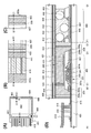
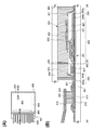
도 1의 (A)는 본 발명의 일 형태의 표시 장치의 평면도를 도시한 것이다. 도 1의 (B)는 도 1의 (A)에서의 일점 쇄선 A1-B1간을 확대한 평면도, 도 1의 (C)는 도 1의 (A)에서의 일점 쇄선 D1-E1간을 확대한 평면도, 도 1의 (D)는 도 1의 (A)에서의 일점 쇄선 A1-B1간, C1-D1간, D1-E1간, 및 F1-G1간의 단면도를 도시한 것이다. 또한, 본 실시형태에서 사용하는 평면도에서는, 일부 구성을 생략하여 도시한 경우가 있다.1A is a plan view of a display device of one embodiment of the present invention. FIG. 1B is an enlarged plan view of one-dot chain line A1-B1 in FIG. 1A, and FIG. 1C is an enlarged view of one-dot chain line D1-E1 in FIG. 1A. 1D shows a cross-sectional view between dashed-dotted lines A1-B1, C1-D1, D1-E1, and F1-G1 in FIG. 1A. In addition, in the top view used by this embodiment, some structures may be abbreviate | omitted and shown.
도 1의 (A)에 도시된 표시 장치는, 기판(401) 위에 화소부(402), 신호선 구동 회로(403), 주사선 구동 회로(404), 및 FPC(Flexible Printed Circuit)(418)를 갖는다. 시일재(405)는 화소부(402), 신호선 구동 회로(403), 및 주사선 구동 회로(404)를 둘러싸도록 프레임 형상으로 배치되고, 기판(401) 및 기판(406)을 접착시킨다. 표시 장치는 구동 회로를 보호하기 위한 보호 회로를 추가적으로 구비하여도 좋다.The display device shown in FIG. 1A includes a
신호선 구동 회로(403) 및 주사선 구동 회로(404)는 복수의 트랜지스터를 갖는다. 신호선 구동 회로(403) 및 주사선 구동 회로(404)에는 각종 CMOS회로, PMOS회로, 또는 NMOS회로를 사용할 수 있다. 본 발명의 일 형태에서는, 트랜지스터를 포함한 구동 회로의 일부 또는 전체를 화소부가 형성되는 절연 표면 위에 일체로 형성하여 시스템 온 패널(system on panel)을 형성할 수 있다. 또는 화소부가 형성되는 절연 표면과는 다른 위치에 구동 회로를 제공하는 구성으로 하여도 좋다.The signal
기판(401) 위에는 구동 회로에 외부로부터의 신호(비디오 신호, 클록 신호, 스타트 신호, 또는 리셋 신호 등)나 전위를 전달하는 외부 입력 단자를 접속하기 위한 리드 배선(lead wiring)이 제공된다. 여기서는, 외부 입력 단자로서 FPC(418)이 제공되어 있는 예를 나타낸다. 또한, FPC(418)에는 프린트 배선 기판(PWB)이 장착되어 있어도 좋다.On the
화소부(402)가 구비한 표시 소자로서는, 액정 소자(액정 표시 소자), 발광 소자(발광 표시 소자) 등을 사용할 수 있다. 발광 소자는, 전류 또는 전압에 의하여 휘도가 제어되는 소자를 그 범주에 포함하고, 구체적으로는 무기 EL(Electroluminescence) 소자, 유기 EL 소자 등이 포함된다.As a display element with which the
또한, 표시 장치로서 전자 잉크를 구동시키는 전자 페이퍼를 제공할 수도 있다. 전자 페이퍼는, 전기 영동 표시 장치(전기 영동 디스플레이)라고도 불리고, 종이와 같이 읽기 쉽고, 다른 표시 장치와 비교하여 소비 전력이 낮으며, 얇고 가벼운 형상으로 할 수 있는 이점을 갖는다Further, it is also possible to provide an electronic paper for driving electronic ink as a display device. Electronic paper, also called an electrophoretic display (electrophoretic display), is easy to read like paper, has a low power consumption compared to other display devices, and has the advantage of being thin and light in shape.
표시 장치의 화소부(402) 및 구동 회로는 각각 복수의 트랜지스터를 갖는다. 본 발명의 일 형태가 적용된 표시 장치에서는, 산화물 반도체를 사용한 트랜지스터를 화소부(402)에 구비하여도 좋고, 화소부(402)와 같은 기판에 형성된 구동 회로에 구비하여도 좋다. 적어도 한 쌍의 기판이 시일재(405)로 접착되어 생기는 공간 내에 산화물 반도체를 사용한 트랜지스터가 하나 이상 제공되어 있으면 좋다. 도 1의 (D)에서는 화소부(402)에 포함된 산화물 반도체를 사용한 트랜지스터(251)를 예시하였다.The
트랜지스터(251)는 기판(401) 위의 게이트 전극(201), 게이트 전극(201) 위의 게이트 절연막(203), 게이트 절연막(203)을 개재(介在)하여 게이트 전극(201)과 중첩되는 산화물 반도체층(205), 및 산화물 반도체층(205)과 전기적으로 접속되는 한 쌍의 전극(207a, 207b)(소스 전극 및 드레인 전극)을 갖는다. 트랜지스터(251)가 구비하는 게이트 절연막(203)은 게이트 전극(201)과 접하는 제 1 게이트 절연막(203a)과, 산화물 반도체층(205)과 접하는 제 2 게이트 절연막(203b)을 갖는다.The
또한, 화소부(402)에는 트랜지스터(251)를 덮는 보호막(209)이 제공되어 있다. 보호막(209)은 산화물 반도체층(205)과 접하는 제 1 보호막(209a)과, 제 1 보호막(209a) 위의 제 2 보호막(209b)을 갖는다.In addition, the
본 실시형태에서는 제 1 게이트 절연막(203a)으로서 질화 실리콘막을 사용하고, 제 2 게이트 절연막(203b)으로서 질소를 포함한 산화 실리콘막을 사용한다.In this embodiment, a silicon nitride film is used as the first
본 실시형태에서는 제 1 보호막(209a)으로서 질소를 포함한 산화 실리콘막을 사용하고, 제 2 보호막(209b)으로서 질화 실리콘막을 사용한다.In this embodiment, a silicon oxide film containing nitrogen is used as the first
다만, 각 구성예에 있어서 시일재(405)와 접하는 층 이외는 반드시 질소를 포함한 무기 절연막이 아니라도 좋다.In addition, in each structural example, it may not necessarily be an inorganic insulating film containing nitrogen other than the layer which contacts the sealing
또한, 본 실시형태에 있어서, 제 2 게이트 절연막(203b) 및 제 1 보호막(209a)은 모두 질소를 포함한 산화 실리콘막이기 때문에, 제 2 게이트 절연막(203b) 및 제 1 보호막(209a)이 접하여 제공된 영역에서는, 제 1 보호막(209a)을 에칭할 때 제 2 게이트 절연막(203b)도 동시에 제거되는 경우가 있다. 따라서, 본 실시형태에서는, 에칭 등에 의하여 제 1 보호막(209a)을 제거한 영역에는 제 2 게이트 절연막(203b)을 도시하지 않은(제 1 보호막(209a)과 접하는 제 2 게이트 절연막(203b)도 제거된 것으로 함) 경우가 있지만, 이것에 한정되지 않는다.In the present embodiment, since the second
또한, 보호막(209) 위에는, 유기 절연막(407)이 제공되고, 유기 절연막(407) 위에는 트랜지스터(251)와 전기적으로 접속하는 액정 소자(260)가 제공되어 있다. 액정 소자(260)는 기판 면에 대하여 세로 방향으로 전계를 발생시키는 방식(세로 전계 방식)의 액정 소자이다. 액정 소자(260)는 전극(207b)과 전기적으로 접속되는 하부 전극(421)과, 기판(406) 위에 제공된 상부 전극(422)과 액정층(423)을 포함한다.An organic insulating
하부 전극(421)과 액정층(423) 사이, 및 상부 전극(422)과 액정층(423) 사이에는, 액정층(423)을 협지하도록 배향막(424)으로서 기능하는 절연막이 각각 제공되어 있다.Between the
또한, 스페이서(425)는 절연막을 선택적으로 에칭하여 얻어지는 기둥 형상의 스페이서이며 액정층(423)의 막 두께(셀 갭)를 제어하기 위하여 제공되어 있다. 또한 구(球) 형상의 스페이서를 사용하여도 좋다.The
또한, 배선(415) 및 배선(441)은 이방성 도전막(419)을 개재하여 FPC(418)와 전기적으로 접속되어 있다. 본 실시형태에서는, 배선(441)의 재료로서 인듐 주석 산화물 등의 도전성 산화물을 사용한다. 여기서, 배선(415)이 제 1 게이트 절연막(203a)으로 덮이지 않은 영역에 배선(441)을 형성하면 배선(415)의 산화를 방지할 수 있어 바람직하다. 다만, 배선(415)이 산화되기 어려운 재료나 도전성 산화물로 이루어진 경우에는 배선(441)은 제공하지 않아도 좋다. 또한, 배선(415)이 제 1 게이트 절연막(203a)으로 덮여 있기 때문에 시일재(405)와 접하는 층이 질소를 포함한 무기 절연막이 됨으로써 시일재(405)와의 밀착성이 높아져 바람직하다. 배선(415)은 트랜지스터(251)의 게이트 전극(201)과 같은 도전층으로 형성되고, 배선(441)은 액정 소자(260)의 하부 전극(421)과 같은 도전층으로 형성되어 있다. 본 실시형태에서 기재하는 각 구성예에서 나타내는 바와 같이 소자를 구성하는 도전층과 같은 재료, 같은 공정으로 배선을 제작함으로써 표시 장치의 제작 공정을 간략화할 수 있어 바람직하다.The
또한, 기판(406) 위에는 하지막(432)이 제공되고, 하지막(432) 위에 컬러 필터(413) 및 블랙 매트릭스(414)가 제공되고, 컬러 필터(413) 및 블랙 매트릭스(414) 위에 오버 코트층(412)이 제공되어 있다.In addition, an
도 1의 (A) 및 (D)에 도시된 바와 같이, 구성예 1에서는, 기판(401) 및 기판(406)이 시일재(405)로 접착된 외부에, 액정 소자(260)의 공통 접속부(440)(코먼 콘택트(common contact)부)를 갖는 경우를 도시하였다.As shown in FIGS. 1A and 1D, in the structural example 1, the common connection portion of the
공통 접속부(440)에 있어서, 기판(401) 위에는 게이트 절연막(203)과, 게이트 절연막(203) 위의 배선(447)과, 배선(447) 위의 배선(448)이 제공되어 있고, 기판(406) 위에는, 하지막(432)과, 하지막(432) 위의 블랙 매트릭스(414)와, 블랙 매트릭스(414) 위의 오버 코트층(412)과, 오버 코트층(412) 위의 상부 전극(422)이 제공되어 있다. 기판(401) 및 기판(406) 사이에는, 도전성 입자(446)를 포함한 수지층(445)이 제공되어 있고, 도전성 입자(446)에 의하여 기판(401) 위의 배선(447) 및 배선(448)과, 기판(406) 위의 상부 전극(422)이 전기적으로 접속된다. 수지층(445)에는, 시일재(405)에 사용할 수 있는 수지를 적용할 수 있고, 시일재(405)와 같은 재료를 사용하여도 좋고, 상이한 재료를 사용하여도 좋다.In the common connecting
여기서, 구성예 1에서는 시일재(405)와 제 1 게이트 절연막(203a)이 접한다. 제 1 게이트 절연막(203a)은 질소를 포함한 무기 절연막이기 때문에, 수소나 물 등의 블로킹 효과가 높다. 또 시일재(405)와 제 1 게이트 절연막(203a)의 밀착성은 높다. 따라서, 장치의 외부에 존재하는 수소나 물이 시일재(405)와 제 1 게이트 절연막(203a)의 계면이나 제 1 게이트 절연막(203a) 중에 혼입되는 것을 억제할 수 있다. 따라서, 장치의 외부에 존재하는 수소나 물이 트랜지스터(251)에 포함되는 산화물 반도체 중에 혼입되는 것을 억제할 수 있다. 또한, 제 1 게이트 절연막(203a)은 기판(401)에 포함되는 수분 등이 산화물 반도체층(205)에 혼입되는 것을 억제할 수 있다.Here, in the structural example 1, the sealing
또한, 트랜지스터에 포함된 산화물 반도체층(205)은 게이트 절연막(203) 및 보호막(209)에 의하여 전체가 덮여 있다. 이와 같은 구성으로 함으로써 게이트 절연막(203)보다 기판(401) 측에 제공된 기판(401) 위의 각 층(예를 들어, 하지막이나 기판(401) 등), 및 보호막(209)보다 기판(406) 측에 제공된 기판(401) 위의 각 층(예를 들어, 유기 절연막(407), 표시 소자나 발광 소자 등)에 포함된 수분 등의 불순물이 산화물 반도체층(205)에 혼입되는 것을 억제할 수 있어 바람직하다.The
도 1의 (B) 내지 (D)에 도시된 바와 같이, 구성예 1에서는 유기 절연막(407)의 단부 측면의 외측에 시일재(405)가 제공되어, 유기 절연막(407)의 단부 측면이 대기에 노출되지 않는다. 따라서, 대기 중의 수분 등이 유기 절연막(407)을 통하여 표시 장치의 내부, 또한 트랜지스터의 내부(산화물 반도체 등)에 혼입되는 것을 억제할 수 있다.As shown in Figs. 1B to 1D, in the structural example 1, the sealing
<구성예 2>≪ Configuration Example 2 &
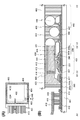
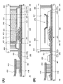
도 2의 (A)에 본 발명의 일 형태의 표시 장치의 평면도를 도시하였다. 도 2의 (B)는 도 2의 (A)에서의 일점 쇄선 A2-B2간, C2-D2간, 및 E2-F2간의 단면도를 도시한 것이다.2A is a plan view of the display device of one embodiment of the present invention. FIG. 2B illustrates a cross-sectional view between dashed-dotted lines A2-B2, C2-D2, and E2-F2 in FIG.
도 2의 (A)에 도시된 표시 장치는, 기판(401) 위에 화소부(402), 신호선 구동 회로(403), 주사선 구동 회로(404), 및 FPC(418)를 갖는다. 시일재(405)는 화소부(402), 신호선 구동 회로(403), 및 주사선 구동 회로(404)를 둘러싸도록 프레임 형상으로 배치되고, 기판(401) 및 기판(406)을 접착시킨다.The display device shown in FIG. 2A includes a
도 2의 (B)에 도시된 화소부(402)는, 트랜지스터(251)와, 트랜지스터(251)를 덮는 보호막(209)과, 보호막(209) 위의 유기 절연막(407)과, 유기 절연막(407) 위의 액정 소자(260)를 갖는다. 이들의 구성은 구성예 1과 마찬가지므로, 상세한 설명은 생략한다. 또한, 스페이서(425), 배향막(424)으로서 기능하는 절연막, 그리고, 기판(406) 위에 제공된 컬러 필터(413), 블랙 매트릭스(414) 및 오버 코트층(412)에 대해서도 마찬가지다.The
배선(415), 배선(416), 배선(417), 및 배선(441)은 이방성 도전막(419)을 통하여 FPC(418)와 전기적으로 접속되어 있다. 여기서, 배선(416)을 덮는 배선(441)을 형성하면 배선(416)의 산화를 방지할 수 있어 바람직하다. 다만, 배선(416)이 산화되기 어려운 재료나 도전성 산화물로 이루어진 경우에는, 배선(441)은 제공하지 않아도 좋다. 또한, 배선(415)이 제 1 게이트 절연막(203a)으로 덮여 있기 때문에 시일재(405)와 접하는 층이 질소를 포함한 무기 절연막이 됨으로써, 시일재(405)와의 밀착성이 높아져 바람직하다. 배선(415)은 트랜지스터(251)의 게이트 전극과 같은 도전층으로 형성되고, 배선(416) 및 배선(417)은 트랜지스터(251)의 한 쌍의 전극(소스 전극 및 드레인 전극)과 같은 도전층으로 형성되고, 배선(441)은 액정 소자(260)의 하부 전극(421)과 같은 도전층으로 형성되어 있다.The
도 2의 (A) 및 (B)에 도시된 바와 같이, 구성예 2에서는, 기판(401) 및 기판(406)이 시일재(405)로 접착된 내부에, 액정 소자(260)의 공통 접속부(440)(코먼 콘택트부)를 갖는 경우를 도시하였다.As shown in FIGS. 2A and 2B, in the structural example 2, the common connection portion of the
공통 접속부(440)에 있어서, 기판(401) 위에는 게이트 절연막(203)과, 게이트 절연막(203) 위의 배선(447)과, 배선(447) 위의 배선(448)이 제공되어 있고, 기판(406) 위에는, 상부 전극(422)이 제공되어 있다. 공통 접속부(440)는 시일재(405)가 제공된 영역의 일부에 상당한다. 시일재(405) 중, 공통 접속부(440)에 상당한 영역에는, 도전성 입자(446)가 포함된다. 도전성 입자(446)에 의하여 기판(401) 위의 배선(447) 및 배선(448)과, 기판(406) 위의 상부 전극(422)이 전기적으로 접속된다.In the common connecting
여기서, 구성예 2에서는 시일재(405)와 제 1 게이트 절연막(203a)이 접한다. 제 1 게이트 절연막(203a)은 질소를 포함한 무기 절연막이기 때문에, 수소나 물 등의 블로킹 효과가 높다. 또 시일재(405)와 제 1 게이트 절연막(203a)의 밀착성은 높다. 따라서, 장치의 외부에 존재하는 수소나 물이 시일재(405)와 제 1 게이트 절연막(203a)의 계면이나 제 1 게이트 절연막(203a) 중에 혼입되는 것을 억제할 수 있다. 따라서, 장치의 외부에 존재하는 수소나 물이 트랜지스터(251)에 포함되는 산화물 반도체 중에 혼입되는 것을 억제할 수 있다. 또한, 제 1 게이트 절연막(203a)은 기판(401)에 포함되는 수분 등이 산화물 반도체층(205)에 혼입되는 것도 억제할 수 있다.Here, in the structural example 2, the sealing
또한, 트랜지스터에 포함된 산화물 반도체층(205)은 게이트 절연막(203) 및 보호막(209)에 의하여 전체가 덮여 있다. 이와 같은 구성으로 함으로써 게이트 절연막(203)보다 기판(401) 측에 제공된 각 층, 보호막(209)보다 기판(406) 측의 각 층에 포함된 수분 등의 불순물이 산화물 반도체층(205)에 혼입되는 것을 억제할 수 있어 바람직하다.The
또한, 구성예 2에서는 유기 절연막(407)의 단부 측면의 외측에 시일재(405)가 제공되고, 유기 절연막(407)의 단부 측면이 대기에 노출되지 않는다. 따라서, 대기 중의 수분 등이 유기 절연막(407)을 통하여 표시 장치의 내부, 또한 트랜지스터의 내부(산화물 반도체 등)에 혼입되는 것을 억제할 수 있다.In addition, in the structural example 2, the sealing
<구성예 3><Configuration Example 3>
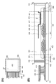
도 3의 (A)에 본 발명의 일 형태의 표시 장치의 평면도를 도시하였다. 도 3의 (B)는 도 3의 (A)에서의 일점 쇄선 A3-B3간의 단면도를 도시한 것이다.3A is a plan view of the display device of one embodiment of the present invention. FIG. 3B shows a cross-sectional view between dashed-dotted lines A3-B3 in FIG. 3A.
도 3의 (A)에 도시된 표시 장치는, 기판(401) 위에 화소부(402), 신호선 구동 회로(403), 주사선 구동 회로(404), 및 FPC(418)를 갖는다. 시일재(405)는 화소부(402), 신호선 구동 회로(403), 및 주사선 구동 회로(404)를 둘러싸도록 프레임 형상으로 배치되고, 기판(401) 및 기판(406)을 접착시킨다. 도 3의 (B)에 도시된 바와 같이, 기판(401) 및 기판(406)이 시일재(405)로 접착되어 생긴 공간(408)에 트랜지스터(251), 트랜지스터(450), 및 발광 소자(270) 등이 제공되어 있다.The display device shown in FIG. 3A includes a
표시 장치의 화소부(402) 및 구동 회로는 각각 복수의 트랜지스터를 갖고, 도 3의 (B)에서는, 화소부(402)에 포함되는 트랜지스터(251) 및 신호선 구동 회로(403)에 포함되는 트랜지스터(450)를 예시한다. 트랜지스터(251)는 구성예 1과 마찬가지므로 상세한 설명은 생략한다. 또한, 트랜지스터(450)는 트랜지스터(251)와 같은 구성이기 때문에 상세한 설명은 생략한다.The
또한, 구동 회로용 트랜지스터(예를 들어, 트랜지스터(450))의 산화물 반도체층의 채널 형성 영역과 중첩되는 위치(예를 들어, 보호막(209) 위나 유기 절연막(407) 위)에 추가적으로 도전층을 제공하여도 좋다. 도전층을 산화물 반도체층의 채널 형성 영역과 중첩하는 위치에 제공함으로써, 트랜지스터의 문턱 전압의 변화량을 저감시킬 수 있다. 상기 도전층의 전위는 트랜지스터의 게이트 전극과 동일하여도 좋고, 상이하여도 좋고, 상기 도전층은 제 2 게이트 전극으로서 기능시킬 수도 있다. 또한, 도전층의 전위가 GND, 0V이어도 좋다.In addition, a conductive layer is additionally provided at a position overlapping the channel formation region of the oxide semiconductor layer of the driving circuit transistor (for example, the transistor 450) (for example, on the
또한, 상기 도전층은 외부의 전장(電場)을 차폐하는 기능, 즉 외부의 전장이 내부(트랜지스터를 포함하는 회로부)에 작용하지 않도록 하는 기능(특히, 정전기에 대한 정전 차폐 기능)도 갖는다. 도전층의 차폐 기능에 의하여, 정전기 등 외부의 전장의 영향으로 트랜지스터의 전기적 특성이 변동되는 것을 방지할 수 있다.The conductive layer also has a function of shielding an external electric field, that is, a function of preventing an external electric field from acting on the inside (a circuit portion including a transistor) (in particular, an electrostatic shielding function against static electricity). Due to the shielding function of the conductive layer, it is possible to prevent variations in the electrical characteristics of the transistor due to the influence of an external electric field such as static electricity.
또한, 화소부(402) 및 신호선 구동 회로(403)에는, 트랜지스터(251) 및 트랜지스터(450)를 덮는 보호막(209)이 제공되어 있다. 보호막(209)의 구성도 구성예 1과 마찬가지므로 상세한 설명은 생략한다.In the
보호막(209) 위에는, 유기 절연막(407)이 제공되고, 유기 절연막(407) 위에는 트랜지스터(251)와 전기적으로 접속되는 발광 소자(270)가 제공되어 있다. 발광 소자(270)로서는, 일렉트로 루미네선스를 이용하는 발광 소자를 적용할 수 있다. 본 실시형태에서는 유기 EL 소자를 사용한다. 발광 소자(270)는 하부 전극(426), 전계 발광층(427), 및 상부 전극(428)을 갖는다. 하부 전극(426) 및 상부 전극(428) 중 적어도 한쪽은 투광성을 갖는다. 하부 전극(426)의 단부는 격벽(429)으로 덮여 있다.An organic insulating
또한, 구성예 3에서는 표시 장치의 단부까지 시일재(405)가 제공되어 있다. 이와 같은 구성은, 나중에 나타내는 구성예 6(도 7의 (A) 참조) 등과 비교하여 프레임 협소화를 도모할 수 있어 바람직하다.In addition, in the structural example 3, the sealing
또한, 배선(415) 및 배선(441)은 이방성 도전막(419)을 통하여 FPC(418)와 전기적으로 접속되어 있다. 여기서, 배선(415)이 제 1 게이트 절연막(203a)으로 덮이지 않은 영역에 배선(441)을 형성하면 배선(415)의 산화를 방지할 수 있어 바람직하다. 또한, 배선(415)이 제 1 게이트 절연막(203a)으로 덮여 있기 때문에 시일재(405)와 접하는 층이 질소를 포함한 무기 절연막이 됨으로써 시일재(405)와의 밀착성이 높아져 바람직하다. 배선(415)은 트랜지스터(251)의 게이트 전극과 같은 도전층으로 형성되고, 배선(441)은 발광 소자(270)의 하부 전극(426)과 같은 도전층으로 형성되어 있다.The
또한, 기판(401) 및 기판(406)의 간격을 조정하는 스페이서나, 유기 EL 소자의 상부 전극과 전기적으로 접속하는 보조 배선을 격벽(429) 위에 제공하여도 좋다.In addition, a spacer for adjusting the distance between the
구성예 3에서는 시일재(405)와 제 1 게이트 절연막(203a)이 접한다. 제 1 게이트 절연막(203a)은 질소를 포함한 무기 절연막이기 때문에, 수소나 물 등의 블로킹 효과가 높다. 또 시일재(405)와 제 1 게이트 절연막(203a)의 밀착성은 높다. 따라서, 장치의 외부에 존재하는 수소나 물이 시일재(405)와 제 1 게이트 절연막(203a)의 계면이나 제 1 게이트 절연막(203a) 중에 혼입되는 것을 억제할 수 있다. 따라서, 장치의 외부에 존재하는 수소나 물이 트랜지스터(251)나 트랜지스터(450)에 포함되는 산화물 반도체 중에 혼입되는 것을 억제할 수 있다. 또한, 제 1 게이트 절연막(203a)은 기판(401)에 포함되는 수분 등이 산화물 반도체층(205)에 혼입되는 것도 억제할 수 있다.In structural example 3, the sealing
또한, 트랜지스터에 포함된 산화물 반도체층(205)은 게이트 절연막(203) 및 보호막(209)에 의하여 전체가 덮여 있다. 이와 같은 구성으로 함으로써 게이트 절연막(203)보다 기판(401) 측의 각 층, 및 보호막(209)보다 기판(406) 측의 각 층에 포함된 수분 등의 불순물이 산화물 반도체층(205)에 혼입되는 것을 억제할 수 있어 바람직하다.The
또한, 구성예 3에서는 유기 절연막(407)의 단부 측면의 외측에 시일재(405)가 제공되어, 유기 절연막(407)의 단부 측면이 대기에 노출되지 않는다. 따라서, 대기 중의 수분 등이 유기 절연막(407)을 통하여 표시 장치의 내부, 또한 트랜지스터의 내부(산화물 반도체 등)에 혼입되는 것을 억제할 수 있다.In addition, in the structural example 3, the sealing
<구성예 4><Configuration example 4>
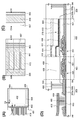
도 4의 (A)에 본 발명의 일 형태의 표시 장치의 평면도를 도시하였다. 도 4의 (B)는 도 4의 (A)에서의 일점 쇄선 A4-B4간을 확대한 평면도, 도 4의 (C)는 도 4의 (A)에서의 일점 쇄선 C4-D4간을 확대한 평면도, 도 4의 (D)는 도 4의 (A)에서의 일점 쇄선 A4-B4간, B4-C4간, 및 C4-D4간의 단면도를 도시한 것이다.4A is a plan view of the display device of one embodiment of the present invention. 4B is an enlarged plan view of one-dot chain line A4-B4 in FIG. 4A, and FIG. 4C is an enlarged view of one-dot chain line C4-D4 in FIG. 4A. 4D illustrates a cross-sectional view between dashed-dotted lines A4-B4, B4-C4, and C4-D4 in FIG. 4A.
도 4의 (A)에 도시된 표시 장치는, 기판(401) 위에 화소부(402), 신호선 구동 회로(403), 주사선 구동 회로(404), 및 FPC(418)를 갖는다. 시일재(405)는 화소부(402), 신호선 구동 회로(403), 및 주사선 구동 회로(404)를 둘러싸도록 프레임 형상으로 배치되고, 기판(401) 및 기판(406)을 접착시킨다.The display device shown in FIG. 4A includes a
도 4의 (D)에 도시된 화소부(402)는, 트랜지스터(251)와, 트랜지스터(251)를 덮는 보호막(209)과, 보호막(209) 위의 유기 절연막(407)과, 유기 절연막(407) 위의 발광 소자(270)를 갖는다. 또한, 도 4의 (D)에 도시된 신호선 구동 회로(403)는, 트랜지스터(450)를 갖는다. 이들의 구성은 구성예 3(도 3의 (B) 참조)과 마찬가지므로, 상세한 설명은 생략한다.The
도 4의 (D)에 도시된 발광 소자(270)는 상부 전극(428)이 투광성을 갖는 상면 사출 구조이다. 기판(406) 위에는 컬러 필터(413) 및 블랙 매트릭스(414)가 제공되어 있다.The
또한, 배선(415) 및 배선(441)은 이방성 도전막(419)을 통하여 FPC(418)와 전기적으로 접속되어 있다. 여기서, 배선(415)이 게이트 절연막(203) 및 보호막(209)으로 덮이지 않은 영역에 배선(441)을 형성하면 배선(415)의 산화를 방지할 수 있어 바람직하다. 또한, 배선(415)이 게이트 절연막(203) 및 보호막(209)으로 덮여 있기 때문에 시일재(405)와 접하는 층이 질소를 포함한 무기 절연막이 됨으로써 시일재(405)와의 밀착성이 높아져 바람직하다. 배선(415)은 트랜지스터(251)의 게이트 전극과 같은 도전층으로 형성되고, 배선(441)은 발광 소자(270)의 하부 전극(426)과 같은 도전층으로 형성되어 있다.The
구성예 4에서는 시일재(405)와 제 2 보호막(209b)이 접한다. 제 2 보호막(209b)은 질소를 포함한 무기 절연막이기 때문에, 수소나 물 등의 블로킹 효과가 높다. 또 시일재(405)와 제 2 보호막(209b)의 밀착성은 높다. 따라서, 장치의 외부에 존재하는 수소나 물이 시일재(405)와 제 2 보호막(209b)의 계면이나 제 2 보호막(209b) 중에 혼입되는 것을 억제할 수 있다. 따라서, 장치의 외부에 존재하는 수소나 물이 트랜지스터(251)나 트랜지스터(450)에 포함되는 산화물 반도체 중에 혼입되는 것을 억제할 수 있다. 또한, 제 2 보호막(209b)은 유기 절연막(407)이나 격벽(429) 등에 포함되는 수분 등이 산화물 반도체층(205)에 혼입되는 것도 억제할 수 있다.In the structural example 4, the sealing
또한, 본 실시형태에서는 제 1 게이트 절연막(203a), 제 2 게이트 절연막(203b), 제 1 보호막(209a), 및 제 2 보호막(209b)은 모두 질소를 포함한 무기 절연막이다. 따라서, 표시 장치의 단부에 이들의 막이 존재하여도 장치의 외부에 존재하는 수소나 물이 이들 막 중에 혼입되는 것을 억제할 수 있다. 따라서, 장치의 외부에 존재하는 수소나 물이 트랜지스터(251)나 트랜지스터(450)에 포함되는 산화물 반도체 중에 혼입되는 것을 억제할 수 있다.In the present embodiment, the first
또한, 트랜지스터에 포함되는 산화물 반도체층(205)은 게이트 절연막(203) 및 보호막(209)에 의하여 전체가 덮여 있다고 표현할 수 있다. 이와 같은 구성으로 함으로써, 게이트 절연막(203)보다 기판(401) 측의 각 층, 및 보호막(209)보다 기판(406) 측의 각 층에 포함되는 수분 등의 불순물이 산화물 반도체층(205)에 혼입되는 것을 억제할 수 있어 바람직하다.The
또한, 기판(406)에 있어서 시일재(405)와 접하는 영역에는 질소를 포함한 무기 절연막(430)이 제공되어 있다. 표시 장치의 구성에 따라서는, 기판(406) 위에 표시 소자의 전극, 컬러 필터, 또는 블랙 매트릭스 등이 제공된다. 이들의 층은, 반드시 시일재(405)와의 밀착성이 높은 층에 한정되지 않는다. 따라서, 기판(406) 위의 시일재(405)와 접하는 층으로서, 질소를 포함한 무기 절연막(430)을 제공하는 것이 바람직하다. 질소를 포함한 무기 절연막(430)을 제공함으로써 기판(401) 측뿐만 아니라 기판(406) 측에서도 시일재(405)와 접하는 층과 시일재(405)의 밀착성이 높아져 표시 장치의 신뢰성을 높일 수 있다.In addition, an inorganic
또한, 도 4의 (B) 내지 (D)에 도시된 바와 같이, 구성예 4에서는 유기 절연막(407)의 단부 측면의 외측에 시일재(405)가 제공되고, 유기 절연막(407)의 단부 측면이 대기에 노출되지 않는다. 따라서, 대기 중의 수분 등이 유기 절연막(407)을 통하여 표시 장치의 내부, 또한 트랜지스터의 내부(산화물 반도체 등)에 혼입되는 것을 억제할 수 있다.4 (B) to (D), in the structural example 4, the sealing
<구성예 5>≪ Configuration Example 5 &
도 5에 터치 패널 기능을 갖는 본 발명의 일 형태가 적용된 표시 장치의 단면도를 도시하였다.5 is a cross-sectional view of a display device to which one embodiment of the present invention having a touch panel function is applied.
도 5에서는 기판(401) 위에 트랜지스터(251)와, 트랜지스터(251)를 덮는 제 1 보호막(209a)과, 제 1 보호막(209a) 위의 제 2 보호막(209b)을 갖는다. 트랜지스터(251)의 구성은 구성예 1(도 1의 (D) 참조) 등과 마찬가지므로, 상세한 설명은 생략한다.In FIG. 5, a
구성예 5에서는 제 1 보호막(209a)의 단부는 제 2 보호막(209b)으로 덮여 있다. 제 1 보호막(209a)의 단부는 기판(401), 기판(406), 및 시일재(405)로 둘러싸인 영역 내에 있고, 시일재(405)는 제 2 보호막(209b)과 접한다. 제 2 보호막(209b)은 질소를 포함한 무기 절연막이기 때문에, 수소나 물 등의 블로킹 효과가 높다. 또 시일재(405)와 제 2 보호막(209b)의 밀착성은 높다. 따라서, 장치의 외부에 존재하는 수소나 물이 시일재(405)와 제 2 보호막(209b)의 계면이나 제 2 보호막(209b) 중에 혼입되는 것을 억제할 수 있다. 따라서, 장치의 외부에 존재하는 수소나 물이 트랜지스터(251)나 트랜지스터(450)에 포함되는 산화물 반도체 중에 혼입되는 것을 억제할 수 있다. 또한, 제 2 보호막(209b)은 유기 절연막(407)이나 격벽(429) 등에 포함되는 수분 등이 산화물 반도체층(205)에 혼입되는 것도 억제할 수 있다.In the structural example 5, the edge part of the 1st
또한, 본 실시형태에서는 제 1 게이트 절연막(203a) 및 제 2 보호막(209b)은 모두 질소를 포함한 무기 절연막이다. 따라서, 표시 장치의 단부에 이들의 막이 존재하여도 장치의 외부에 존재하는 수소나 물이 이들 막 중에 혼입되는 것을 억제할 수 있다. 따라서, 장치의 외부에 존재하는 수소나 물이 트랜지스터(251)나 트랜지스터(450)에 포함되는 산화물 반도체 중에 혼입되는 것을 억제할 수 있다.In the present embodiment, both the first
또한, 트랜지스터에 포함되는 산화물 반도체층(205)은 제 2 게이트 절연막(203b) 및 제 1 보호막(209a)에 의하여 전체가 덮여 있고, 또한 그 외측에서 제 1 게이트 절연막(203a) 및 제 2 보호막(209b)으로도 덮여 있다. 이와 같은 구성으로 함으로써, 장치의 외부에 존재하는 수분 등의 불순물뿐만 아니라 장치 내부에 포함되는 수분 등의 불순물이 산화물 반도체층(205)에 혼입되는 것을 억제할 수 있어 바람직하다.The
제 2 보호막(209b) 위에는, 유기 절연막(407)이 제공되어 있다. 구성예 5에서는 유기 절연막(407)의 단부 측면의 외측에 시일재(405)가 제공되고, 유기 절연막(407)의 단부 측면이 대기에 노출되지 않는다. 따라서, 대기 중의 수분 등이 유기 절연막(407)을 통하여 표시 장치의 내부, 또한 트랜지스터의 내부(산화물 반도체 등)에 혼입되는 것을 억제할 수 있다.On the second
유기 절연막(407) 위에는 액정 소자(261)가 제공되어 있다. 액정 소자(261)는 FFS(Fringe Field Switching) 모드가 적용된 액정 소자이고, 한 쌍의 전극(하부 전극(421) 및 상부 전극(422))이 절연막(420)을 사이에 개재하여 형성되어 있다.The
또한, 상부 전극(422)에는 트랜지스터(251)가 구비한 한 쌍의 전극 중 하나와 전기적으로 접속되어 있다. 도 5에서는, 보호막(209) 및 절연막(420)에 제공되는 콘택트 홀의 크기가, 유기 절연막(407)에 제공되는 콘택트 홀의 크기와 비교하여 작은 경우를 도시하였다. 보호막(209)과 절연막(420)이 접함으로써 유기 절연막(407)이 노출되지 않으므로 콘택트 홀을 통하여 유기 절연막(407)에 포함된 수분 등의 불순물이 트랜지스터(251)의 내부(산화물 반도체 등)에 혼입되는 것을 억제할 수 있어 바람직하다.The
다만, 유기 절연막(407)은 제작 공정 중의 가열 처리 등에 의하여 내부에 잔류하는 수분 등의 불순물을 표시 장치의 외부로 방출할 수 있다. 표시 장치가 완성된 후에 유기 절연막(407) 내에 잔류하는 불순물을 저감할 수 있고, 트랜지스터나 표시 소자의 신뢰성을 높일 수 있다. 따라서, 절연막(420)이 유기 절연막(407) 전체를 덮는 구성보다 절연막(420)이 유기 절연막(407) 위의 일부에만 제공되어 있는 구성이 바람직하다.However, the organic insulating
또한, 배선(416) 및 배선(441)은 이방성 도전막(419a)을 통하여 FPC(418a)와 전기적으로 접속되어 있다. 여기서, 배선(416)이 보호막(209)으로 덮이지 않은 영역에 배선(441)을 형성하면 배선(416)의 산화를 방지할 수 있어 바람직하다. 또한, 배선(416)이 보호막(209)으로 덮여 있기 때문에 시일재(405)와 접하는 층이 질소를 포함한 무기 절연막이 됨으로써, 시일재(405)와의 밀착성이 높아져 바람직하다. 배선(416)은 트랜지스터(251)의 소스 전극 및 드레인 전극과 같은 도전층으로 형성되고, 배선(441)은 액정 소자(261)의 한 쌍의 전극 중 적어도 하나와 같은 도전층으로 형성되어 있다.The
기판(406)은 수지층(410)을 개재하여 기판(409)과 접착된다. 기판(409)에는 터치 패널용의 전극(442) 및 전극(443)이 층간 절연막(444)을 개재하여 제공된다. 이들 구성을 포함함으로써 본 발명의 일 형태의 표시 장치에 터치 패널의 기능을 구비할 수 있다.The
또한, 배선(449)은 이방성 도전막(419b)을 통하여 FPC(418b)와 전기적으로 접속되어 있다. 배선(449)은 터치 패널용의 전극(443)과 같은 도전층으로 형성되어 있다.The
또한, 기판(406)과 수지층(410) 사이에는, 편광 필름이나 대전 방지층을 적절히 제공할 수 있다.In addition, a polarizing film or an antistatic layer can be appropriately provided between the
<구성예 6>≪ Configuration Example 6 &
도 6의 (A)에 본 발명의 일 형태의 표시 장치의 평면도를 도시하였다. 도 6의 (B)는 도 6의 (A)에서의 일점 쇄선 A5-B5간을 확대한 평면도, 도 6의 (C)는 도 6의 (A)에서의 일점 쇄선 D5-E5간을 확대한 평면도, 도 6의 (D)는 도 6의 (A)에서의 일점 쇄선 A5-B5간, C5-D5간, 및 D5-E5간의 단면도를 도시한 것이다.6A is a plan view of a display device of one embodiment of the present invention. FIG. 6B is a plan view enlarged between the one-dot chain lines A5-B5 in FIG. 6A, and FIG. 6C is an enlarged view between the one-dot chain lines D5-E5 in FIG. 6A. 6D shows a cross-sectional view between dashed-dotted lines A5-B5, C5-D5, and D5-E5 in FIG. 6A.
도 6의 (A)에 도시된 표시 장치는, 기판(401) 위에 화소부(402), 신호선 구동 회로(403), 주사선 구동 회로(404), 및 FPC(418)를 갖는다. 시일재(405)는 화소부(402), 신호선 구동 회로(403), 및 주사선 구동 회로(404)를 둘러싸도록 프레임 형상으로 배치되고, 기판(401) 및 기판(406)을 접착시킨다.The display device shown in FIG. 6A includes a
도 6의 (D)에 도시된 화소부(402)는, 트랜지스터(251)와, 트랜지스터(251)를 덮는 보호막(209)과, 보호막(209) 위의 유기 절연막(407)과, 유기 절연막(407) 위의 액정 소자(261)를 갖는다. 트랜지스터(251), 보호막(209), 및 유기 절연막(407)의 구성은 구성예 1(도 1 참조)과 마찬가지고, 액정 소자(261)의 구성은 구성예 5(도 5 참조)와 마찬가지므로, 상세한 설명은 생략한다.The
또한, 구성예 6에서는, 액정층(423)에 블루상을 발현하는 액정 조성물을 사용하는 경우를 나타낸다. 블루상을 발현하는 액정 조성물을 사용하면 배향막이 불필요해지기 때문에, 제작 공정을 간략화할 수 있어 바람직하다.In addition, in the structural example 6, the case where the liquid crystal composition which expresses a blue phase is used for the
또한, 배선(416)은 이방성 도전막(419)을 통하여 FPC(418)와 전기적으로 접속되어 있다. 배선(416)은 트랜지스터(251)의 한 쌍의 전극(소스 전극 및 드레인 전극)과 같은 도전층으로 형성되어 있다.The
구성예 6에서는, 시일재(405)와 질소를 포함한 무기 절연막(431)이 접한다. 무기 절연막(431)은 액정 소자(261)가 구비한 절연막(420)과 같은 절연막으로 형성되고, 본 실시형태에서는 질화 실리콘막을 사용한다. 무기 절연막(431)은 수소나 물 등의 블로킹 효과가 높다. 또 시일재(405)와 무기 절연막(431)의 밀착성은 높다. 따라서, 장치의 외부에 존재하는 수소나 물이 시일재(405)와 무기 절연막(431)의 계면이나 무기 절연막(431) 중에 혼입되는 것을 억제할 수 있다. 따라서, 장치의 외부에 존재하는 수소나 물이 트랜지스터(251)에 포함되는 산화물 반도체 중에 혼입되는 것을 억제할 수 있다.In the structural example 6, the sealing
무기 절연막(431)은 질소를 포함한 무기 절연막이고, 예를 들어 질화 실리콘막, 질화 산화 실리콘막 등을 사용할 수 있다. 또한, 실시형태 2에서 설명하는 게이트 절연막이나 보호막에 사용할 수 있는 질소를 포함한 무기 절연막을 무기 절연막(431)으로서 사용할 수 있다.The inorganic
또한, 트랜지스터(251)에 포함되는 산화물 반도체층(205)은 게이트 절연막(203) 및 보호막(209)에 의하여 전체가 덮여 있다. 이와 같은 구성으로 함으로써, 게이트 절연막(203)보다 기판(401) 측의 각 층, 및 보호막(209)보다 기판(406) 측의 각 층에 포함되는 수분 등의 불순물이 산화물 반도체층(205)에 혼입되는 것을 억제할 수 있어 바람직하다.The
또한, 도 6의 (B) 내지 (D)에 도시된 바와 같이, 구성예 6에서는 유기 절연막(407)의 단부 측면의 외측에 시일재(405)가 제공되고, 유기 절연막(407)의 단부 측면이 대기에 노출되지 않는다. 따라서, 대기 중의 수분 등이 유기 절연막(407)을 통하여 표시 장치의 내부, 또한 트랜지스터의 내부(산화물 반도체 등)에 혼입되는 것을 억제할 수 있다.6 (B) to (D), in the structural example 6, the sealing
<구성예 7>≪ Configuration Example 7 &
도 7의 (A)에 본 발명의 일 형태의 표시 장치의 평면도를 도시하였다. 도 7의 (B)는 도 7의 (A)에서의 일점 쇄선 A6-B6간 및 C6-D6간의 단면도를 도시한 것이다.7A is a plan view of the display device of one embodiment of the present invention. FIG. 7B shows a cross-sectional view between dashed-dotted lines A6-B6 and C6-D6 in FIG. 7A.
도 7의 (B)에서는, 기판(401) 위에 트랜지스터(251)와, 트랜지스터(251)를 덮는 보호막(209)을 갖는다. 이들의 구성은 구성예 1 등과 마찬가지므로 상세한 설명은 생략한다.In FIG. 7B, a
보호막(209) 위에는, 유기 절연막(407)이 제공되어 있다. 구성예 7에서는 유기 절연막(407)의 단부 측면의 외측에 시일재(405)가 제공되고, 유기 절연막(407)의 단부 측면이 대기에 노출되지 않는다. 따라서, 대기 중의 수분 등이 유기 절연막(407)을 통하여 표시 장치의 내부, 또한 트랜지스터의 내부(산화물 반도체 등)에 혼입되는 것을 억제할 수 있다.On the
또한, 유기 절연막(407) 위에는 액정 소자(261)가 제공되어 있다. 액정 소자(261)는 FFS 모드가 적용된 액정 소자이고, 한 쌍의 전극(하부 전극(421) 및 상부 전극(422))이 절연막(420)을 사이에 개재하여 형성되어 있다. 또한 하부 전극(421)은 트랜지스터(251)가 구비한 한 쌍의 전극 중 하나와 전기적으로 접속되어 있다.The
또한, 배선(415), 배선(416), 배선(417) 및 배선(441)은 이방성 도전막(419)을 통하여 FPC(418)와 전기적으로 접속되어 있다. 여기서, 배선(416)을 덮는 배선(441)을 형성하면 배선(416)의 산화를 방지할 수 있어 바람직하다. 또한, 배선(441)이 무기 절연막(431)으로 덮여 있기 때문에 시일재(405)와 접하는 층이 무기 절연막(431)이 됨으로써, 시일재(405)와의 밀착성이 높아져 바람직하다. 배선(415)은 트랜지스터(251)의 게이트 전극과 같은 도전층으로 형성되고, 배선(416) 및 배선(417)은 트랜지스터(251)의 한 쌍의 전극(소스 전극 및 드레인 전극)과 같은 도전층으로 형성되고, 배선(441)은 액정 소자(261)의 하부 전극(421) 또는 상부 전극(422)과 같은 도전층으로 형성되고, 무기 절연막(431)은 절연막(420)과 같은 절연막으로 형성되어 있다.The
구성예 7에서는, 시일재(405)와 질소를 포함한 무기 절연막(431)이 접한다. 무기 절연막(431)은 액정 소자(261)가 구비한 절연막(420)과 같은 절연막으로 형성되고, 본 실시형태에서는 질화 실리콘막을 사용한다. 무기 절연막(431)은 수소나 물 등의 블로킹 효과가 높다. 또 시일재(405)와 무기 절연막(431)의 밀착성은 높다. 따라서, 장치의 외부에 존재하는 수소나 물이 시일재(405)와 무기 절연막(431)의 계면이나 무기 절연막(431) 중에 혼입되는 것을 억제할 수 있다. 따라서, 장치의 외부에 존재하는 수소나 물이 트랜지스터(251)에 포함되는 산화물 반도체 중에 혼입되는 것을 억제할 수 있다.In the structural example 7, the sealing
또한, 트랜지스터에 포함되는 산화물 반도체층(205)은 게이트 절연막(203) 및 보호막(209)에 의하여 전체가 덮여 있다. 이와 같은 구성으로 함으로써, 장치의 외부에 존재하는 수분 등의 불순물뿐만이 아니라 장치 내부에 포함되는 수분 등의 불순물이 산화물 반도체층(205)에 혼입되는 것을 억제할 수 있어 바람직하다.The
이와 같이, 본 발명의 일 형태를 적용함으로써 기판(401), 기판(406), 및 시일재(405)로 둘러싸인 공간의 외부에 존재하는 수분 등의 불순물이 트랜지스터(산화물 반도체 등)에 혼입되는 것이 억제된 신뢰성이 높은 표시 장치를 실현할 수 있다.Thus, by applying one embodiment of the present invention, it is possible that impurities such as moisture present in the outside of the space surrounded by the
또한, 본 실시형태에서는 제 1 게이트 절연막(203a) 및 무기 절연막(431)은 모두 질소를 포함한 무기 절연막이다. 따라서, 표시 장치의 단부에 이들의 막이 존재하여도 장치의 외부에 존재하는 수소나 물이 이들 막 중에 혼입되는 것을 억제할 수 있다. 따라서, 장치의 외부에 존재하는 수소나 물이 트랜지스터(251)에 포함되는 산화물 반도체 중에 혼입되는 것을 억제할 수 있다.In the present embodiment, both of the first
<구성예 8>≪ Configuration Example 8 &
도 8의 (A)에 도 7의 (A)에서의 일점 쇄선 A6-B6간 및 C6-D6간의 단면도의 다른 예를 도시하였다.Another example of the cross section between the dashed-dotted lines A6-B6 and C6-D6 in FIG. 7A is shown in FIG.
도 8의 (A)에 도시된 화소부(402)는, 트랜지스터(251)와, 트랜지스터(251)를 덮는 보호막(209)을 갖는다. 이들의 구성은 구성예 1(도 1 참조)과 마찬가지므로, 상세한 설명은 생략한다. 또한, 스페이서(425) 및 배향막(424)으로서 기능하는 절연막에 대해서도 마찬가지다.The
보호막(209) 위에는, 유기 절연막(407)이 제공되고, 유기 절연막(407) 위에는 액정 소자(262)가 제공되어 있다. 액정 소자(262)는 가로 전계 방식의 일례인 IPS(In-Plane-Switching) 모드가 적용된 액정 소자이고, 한 쌍의 전극(하부 전극(421) 및 상부 전극(422))이 동일 면 위(여기서는 유기 절연막(407) 위)에 형성되어 있다. 또한, 하부 전극(421)은 트랜지스터(251)가 구비한 한 쌍의 전극 중 하나와 전기적으로 접속되어 있다.The organic
또한, 배선(416)은 이방성 도전막(419)을 통하여 FPC(418)와 전기적으로 접속되어 있다. 배선(416)은 트랜지스터(251)의 한 쌍의 전극(소스 전극 및 드레인 전극)과 같은 도전층으로 형성되어 있다.The
구성예 8에서는, 시일재(405)와 질소를 포함한 무기 절연막(431)이 접한다. 무기 절연막(431)으로서는 질화 실리콘막을 사용한다. 무기 절연막(431)은 수소나 물 등의 블로킹 효과가 높다. 또 시일재(405)와 무기 절연막(431)의 밀착성은 높다. 따라서, 장치의 외부에 존재하는 수소나 물이 시일재(405)와 무기 절연막(431)의 계면이나 무기 절연막(431) 중에 혼입되는 것을 억제할 수 있다. 따라서, 장치의 외부에 존재하는 수소나 물이 트랜지스터(251)에 포함되는 산화물 반도체 중에 혼입되는 것을 억제할 수 있다.In the structural example 8, the sealing
구성예 8에서는 질소를 포함한 무기 절연막(431)이 유기 절연막(407)의 외측 영역으로부터 유기 절연막(407)의 단부 측면 및 단부 상면을 덮기 때문에, 유기 절연막(407)의 단부 측면이 대기에 노출되지 않는다. 따라서, 대기 중의 수분 등이 유기 절연막(407)을 통하여 표시 장치의 내부, 또한 트랜지스터의 내부(산화물 반도체 등)에 혼입되는 것을 억제할 수 있다. 또 유기 절연막(407) 위에 시일재(405)를 형성함으로써, 표시 장치의 프레임 협소화를 도모할 수 있어 바람직하다.In Structural Example 8, since the inorganic
또한, 트랜지스터에 포함된 산화물 반도체층(205)은 게이트 절연막(203) 및 보호막(209)에 의하여 전체가 덮여 있다. 이와 같은 구성으로 함으로써 장치의 외부에 존재하는 수분 등의 불순물뿐만 아니라, 장치 내부에 포함되는 수분 등의 불순물이 산화물 반도체층(205)에 혼입되는 것을 억제할 수 있어 바람직하다.The
또한, 본 실시형태에서는 제 1 게이트 절연막(203a), 제 2 게이트 절연막(203b), 제 1 보호막(209a), 제 2 보호막(209b) 및 무기 절연막(431)은 모두 질소를 포함한 무기 절연막이다. 따라서, 표시 장치의 단부에 이들의 막이 존재하여도 장치의 외부에 존재하는 수소나 물이 이들 막 중에 혼입되는 것을 억제할 수 있다. 따라서, 장치의 외부에 존재하는 수소나 물이 트랜지스터에 포함되는 산화물 반도체 중에 혼입되는 것을 억제할 수 있다.In the present embodiment, the first
<구성예 9>≪ Configuration Example 9 &
도 8의 (B)에 도 7의 (A)에서의 일점 쇄선 A6-B6간 및 C6-D6간의 단면도의 다른 예를 도시하였다.Another example of the cross section between the dashed-dotted lines A6-B6 and C6-D6 in FIG. 7A is shown in FIG.
도 8의 (B)에 도시된 화소부(402)는, 트랜지스터(251)와, 트랜지스터(251)를 덮는 보호막(209)과, 보호막(209) 위의 유기 절연막(407)과, 유기 절연막(407) 위의 발광 소자(270)를 갖는다. 이들의 구성은 구성예 3(도 3의 (B) 참조)과 마찬가지므로, 상세한 설명은 생략한다.The
구성예 9에서는, 시일재(405)와 질소를 포함한 무기 절연막(431)이 접한다. 무기 절연막(431)으로서는 질화 실리콘막을 사용한다. 무기 절연막(431)은 수소나 물 등의 블로킹 효과가 높다. 또 시일재(405)와 무기 절연막(431)의 밀착성은 높다. 따라서, 장치의 외부에 존재하는 수소나 물이 시일재(405)와 무기 절연막(431)의 계면이나 무기 절연막(431) 중에 혼입되는 것을 억제할 수 있다. 따라서, 장치의 외부에 존재하는 수소나 물이 트랜지스터(251)에 포함되는 산화물 반도체 중에 혼입되는 것을 억제할 수 있다.In the structural example 9, the sealing
또한, 구성예 9에서는 유기 절연막(407)의 단부 측면의 외측에 시일재(405)가 제공되어, 유기 절연막(407)의 단부 측면이 대기에 노출되지 않는다. 따라서, 대기 중의 수분 등이 유기 절연막(407)을 통하여 표시 장치의 내부, 또한 트랜지스터의 내부(산화물 반도체 등)에 혼입되는 것을 억제할 수 있다.In addition, in the structural example 9, the sealing
또한, 트랜지스터에 포함되는 산화물 반도체층(205)은 게이트 절연막(203) 및 보호막(209)에 의하여 전체가 덮여 있다. 이와 같은 구성으로 함으로써, 장치의 외부에 존재하는 수분 등의 불순물뿐만 아니라 장치 내부에 포함되는 수분 등의 불순물이 산화물 반도체층(205)에 혼입되는 것을 억제할 수 있어 바람직하다.The
이와 같이, 본 발명의 일 형태를 적용함으로써 기판(401), 기판(406), 및 시일재(405)로 둘러싸인 공간의 외부에 존재하는 수분 등의 불순물이 트랜지스터(산화물 반도체 등)에 혼입되는 것이 억제된 신뢰성이 높은 표시 장치를 실현할 수 있다. 따라서, 상기 공간의 외측에 유기 절연막(407)과 같은 유기 재료로 형성된 층(예를 들어 배선(416) 위에 제공된 수지층(490) 등)이 존재하여도 이들의 층에 포함되는 수분 등의 불순물에 의하여 트랜지스터나 표시 장치의 신뢰성이 저하되는 것을 억제할 수 있다.Thus, by applying one embodiment of the present invention, it is possible that impurities such as moisture present in the outside of the space surrounded by the
이하에서는 본 발명의 일 형태의 표시 장치에 사용할 수 있는 재료의 일례를 기재한다.Below, an example of the material which can be used for the display apparatus of one form of this invention is described.
[기판][Board]
기판(401) 및 기판(406)으로서는, 적어도 제작 공정 중의 가열 처리에 견딜 수 있을 정도의 내열성을 갖는 재료를 사용한다. 예를 들어, 유리 기판, 세라믹 기판, 석영 기판, 사파이어 기판 등을 사용할 수 있다. 또한, 실리콘이나 탄화 실리콘 등의 단결정 반도체 기판이나 다결정 반도체 기판, 실리콘 게르마늄 등의 화합물 반도체 기판, SOI 기판 등을 적용할 수도 있다.As the board |
또한, 기판(401)으로서, 가요성 기판을 사용하고, 가요성 기판 위에 직접 하지막이나 트랜지스터를 형성하여도 좋다. 또한, 기판(401)과 하지막 사이에 박리층을 제공하여도 좋다. 박리층은, 그 위에 소자를 일부 또는 전부 완성시킨 후, 기판(401)으로부터 분리하고, 다른 기판에 전재(轉載)하는 데에 사용할 수 있다. 이 때, 트랜지스터는 내열성이 떨어지는 기판이나 가요성 기판에도 전재할 수 있다.As the
[하지막][Bottom film]
기판(401) 위의 하지막은, 필요하지 않으면 제공하지 않아도 좋지만, 트랜지스터의 특성 안정화 등을 위하여 제공하는 것이 바람직하다. 하지막으로서는, 산화 실리콘막, 산화 질화 실리콘막, 질화 실리콘막, 질화 산화 실리콘막, 산화 갈륨막, 산화 하프늄막, 산화 이트륨막, 산화 알루미늄막, 산화 질화 알루미늄막 등을 사용할 수 있다. 또한, 질화 실리콘막, 산화 갈륨막, 산화 하프늄막, 산화 이트륨막, 산화 알루미늄막 등을 사용함으로써 기판(401)으로부터 불순물(대표적으로는 알칼리 금속, 물, 수소 등)이 산화물 반도체층(205)으로 확산되는 것을 억제할 수 있다. 또한, 본 명세서 중에서, 산화 질화 실리콘막이란, 그 조성으로서, 질소보다도 산소의 함유량이 많은 막을 가리키고, 질화 산화 실리콘막이란, 그 조성으로서, 산소보다도 질소의 함유량이 많은 막을 가리킨다.The base film on the
[시일재][Sealing materials]
시일재(405)에는, 열 경화 수지, 또는 광 경화 수지 등의 유기 수지나, 유리 등을 사용할 수 있다. 유리 등의 무기 재료는, 수지와 비교하여 투습성이 낮으므로, 시일재(405)에 유리를 사용함으로써 수지를 사용하는 경우와 비교하여 표시 장치의 신뢰성이 높아져 바람직하다.As the sealing
또한, 시일재(405)에 유리를 사용하는 경우, 시일재(405)와 접하는 질소를 포함한 무기 절연막은, 탈 가스 성분이 적은 막인 것이 바람직하다. 글라스 프릿에 가열 처리를 실시할 때, 탈 가스 성분이 적을수록 유리와, 상기 유리와 접하는 층과의 밀착성을 높일 수 있다. 따라서, 실시형태 2에서 나중에 기재하는 함유 수소 농도가 낮은 질소를 포함한 실리콘막이나, 수소 분자의 방출량이 5×10²¹ molecules/cm3 미만이고, 암모니아 분자의 방출량이 1×10²² molecules/cm3 미만인 질화 절연막을 사용하는 것이 바람직하다. 이로써 표시 장치의 신뢰성을 높일 수 있다.In addition, when glass is used for the sealing
또한, 시일재(405)에 유리를 사용하는 경우, 시일재와 접하는 질소를 포함한 무기 절연막이 산소를 포함하는 것이 바람직하다. 글라스 프릿을 포함한 프릿 페이스트는 산소를 포함한 층에 대한 습윤성이 높으므로, 상기 산소를 포함한 층과 시일재는 높은 밀착성을 실현할 수 있다. 따라서, 예를 들어 본 명세서 중에 기재하는 산소 및 질소를 포함한 무기 절연막을, 시일재와 접하는 질소를 포함한 무기 절연막으로서 적합하게 사용할 수 있다.In addition, when glass is used for the sealing
또한, 시일재(405)는 건조제가 함유된 수지층이어도 좋다. 건조제로서는 예를 들어 알칼리 토금속의 산화물(산화 칼슘이나 산화 바륨 등)과 같이, 화학 흡착에 의하여 수분이 흡착되는 물질을 사용할 수 있다. 그 이외의 건조제로서, 제올라이트나 실리카젤 등과 같이, 물리 흡착에 의하여 수분이 흡착되는 물질을 사용하여도 좋다. 건조제가 함유되어 있으면, 밀봉 영역 내의 수분 등 불순물이 저감되고, 트랜지스터 등의 소자의 신뢰성이 향상되어 바람직하다.In addition, the sealing
[공간][space]
공간(408)은 아르곤 가스나 질소 가스 등의 불활성 가스, 또는 유기 수지 등의 고체로 충전되어도 좋고, 감압 분위기이어도 좋다. 또한, 공간(408)에 건조제를 제공하여도 좋다.The
[유기 절연막][Organic Insulation Film]
유기 절연막(407)으로서는 예를 들어, 폴리이미드, 아크릴, 벤조시클로부텐계 수지 등의 유기 재료를 사용할 수 있다. 유기 절연막(407)은 트랜지스터에 기인한 표면 요철을 저감하기 위하여 평탄화 기능을 갖는 절연막인 것이 바람직하다. 또한, 유기 절연막(407)과 저유전율 재료(low-k 재료)나 무기 재료 등을 사용하여 형성한 절연막을 적층시켜도 좋다.As the organic insulating
[격벽][septum]
격벽(429)은 유기 절연 재료, 또는 무기 절연 재료를 사용하여 형성한다. 특히 감광성 수지 재료를 사용하여, 그 개구부의 측벽이 연속된 곡률을 갖도록 형성되는 경사면이 되도록 형성하는 것이 바람직하다.The
[액정 소자][Liquid crystal element]
액정층(423)에는, 서모트로픽 액정, 강유전성 액정, 반강유전성 액정 등을 사용할 수 있다. 이들 액정 재료는 저분자 화합물이라도 고분자 화합물이라도 좋다. 이들 액정 재료(액정 조성물)는, 조건에 따라 콜레스테릭상, 스멕틱상, 큐빅상, 키랄네마틱상, 등방상, 블루상 등을 나타낸다. 블루상을 발현하는 액정 조성물은, 응답 속도가 짧고, 광학적 등방성이기 때문에 배향 처리가 불필요하고, 시야각 의존성이 작다. 또한 배향막을 제공하지 않아도 좋고 러빙 처리도 불필요해지기 때문에, 러빙 처리로 인한 정전 파괴를 방지할 수가 있으며, 제작 공정 중의 표시 장치의 불량이나 파손을 경감할 수 있다. 따라서 표시 장치의 생산성을 향상시키는 것이 가능해진다.As the
표시 장치에는, TN(Twisted Nematic) 모드, IPS 모드, FFS 모드, ASM(Axially Symmetric aligned Micro-cell) 모드, OCB(Optical Compensated Birefringence) 모드, FLC(Ferroelectric Liquid Crystal) 모드, AFLC(Anti Ferroelectric Liquid Crystal) 모드 등을 사용할 수 있다.Display devices include Twisted Nematic (TN) mode, IPS mode, FFS mode, Asymmetrically aligned micro-cell (ASM) mode, Optical Compensated Birefringence (OCB) mode, Ferroelectric Liquid Crystal (FLC) mode, and Anti Ferroelectric Liquid Crystal (AFLC). ) Mode can be used.
또한, 노멀리 블랙형의 표시 장치, 예를 들어 수직 배향(VA) 모드를 채용한 투과형 표시 장치로 하여도 좋다. 수직 배향 모드로서는, 몇 개의 예를 들 수 있는데, 예를 들어, MVA(Multi-Domain Vertical Alignment) 모드, PVA(Patterned Vertical Alignment) 모드, ASV(Advanced Super View) 모드 등을 사용할 수 있다.Further, a normally black display device, for example, a transmissive display device employing a vertical alignment (VA) mode may be used. Some examples of the vertical alignment mode include, for example, a multi-domain vertical alignment (MVA) mode, a patterned vertical alignment (PVA) mode, an advanced super view (ASV) mode, and the like.
또한, 표시 장치에 있어서, 블랙 매트릭스(차광층), 편광 부재, 위상차 부재, 반사 방지 부재 등의 광학 부재(광학 기판) 등은 적절히 제공한다. 예를 들어, 편광 기판 및 위상차 기판에 의한 원 편광을 사용하여도 좋다. 또한, 광원으로서 백 라이트, 사이드 라이트 등을 사용하여도 좋다.In the display device, an optical member (optical substrate) such as a black matrix (light shielding layer), a polarizing member, a retardation member, an antireflection member, or the like is appropriately provided. For example, circularly polarized light by a polarizing substrate and a phase difference substrate may be used. Further, a back light, a side light, or the like may be used as the light source.
또한, 화소부에서의 표시 방식으로서는 프로그레시브 방식이나 인터레이스 방식 등을 사용할 수 있다. 또한, 컬러 표시할 때, 화소에서 제어하는 색 요소는 RGB(R는 적색, G는 녹색, B는 청색을 나타냄)의 3색에 한정되지 않는다. 예를 들어, RGBW(W는 백색을 나타냄), 또는 RGB에, 옐로우(yellow)(황색), 시안(cyan), 마젠타(magenta) 등을 1색 이상 추가한 것이 있다. 또한, 색 요소의 도트마다 그 표시 영역의 크기가 상이하여도 좋다. 다만, 기재하는 발명은 컬러 표시의 표시 장치에 한정되는 것이 아니며, 흑백 표시의 표시 장치에 적용할 수도 있다.As the display method in the pixel portion, a progressive method, an interlace method, or the like can be used. In addition, in color display, the color element controlled by the pixel is not limited to three colors of RGB (R represents red, G represents green, and B represents blue). For example, RGBW (W represents white) or RGB, yellow (yellow), cyan, magenta, etc., have added one or more colors. Further, the size of the display area may be different for each color element dot. However, the invention described is not limited to the display device of the color display, but can also be applied to the display device of the monochrome display.
[컬러 필터, 블랙 매트릭스, 오버 코트층][Color Filter, Black Matrix, Overcoat Layer]
컬러 필터에는 예를 들어 유채색의 투광성 수지를 사용할 수 있다. 유채색의 투광성 수지로서는, 감광성, 비감광성의 유기 수지를 사용할 수 있지만, 감광성의 유기 수지층을 사용하면, 레지스트 마스크의 개수를 삭감할 수 있어 공정이 간략화되기 때문에 바람직하다.As the color filter, for example, colored light transmitting resin can be used. Photochromic and non-photosensitive organic resins can be used as the colored light-transmissive resin, but it is preferable to use a photosensitive organic resin layer because the number of resist masks can be reduced and the process is simplified.
유채색은, 흑색, 회색, 백색 등의 무채색을 제외한 색깔이고, 컬러 필터는 착색된 유채색의 광만을 투과시키는 재료로 형성된다. 유채색으로서는, 적색, 녹색, 청색 등을 사용할 수 있다. 또한, 시안, 마젠타, 옐로우 등을 사용하여도 좋다. 착색된 유채색의 광만을 투과시킨다는 것은 컬러 필터에서의 투과광이 그 유채색의 광의 파장에 피크를 가진다는 것이다. 컬러 필터는 포함시킨 착색 재료의 농도와 광의 투과율의 관계를 고려하여, 최적의 막 두께를 적절히 제어하면 좋다. 예를 들어, 컬러 필터의 막 두께는 1500nm 이상 2000nm 이하로 하면 좋다.The chromatic color is a color except for achromatic colors such as black, gray, and white, and the color filter is formed of a material that transmits only colored chromatic light. As the chromatic color, red, green, blue and the like can be used. Cyan, magenta, yellow, or the like may also be used. Transmitting only colored pigmented light means that the transmitted light in the color filter has a peak at the wavelength of the colored light. What is necessary is just to control an optimum film thickness suitably in consideration of the relationship between the density | concentration of the coloring material contained and the transmittance | permeability of light for a color filter. For example, the thickness of the color filter may be 1500 nm or more and 2000 nm or less.
블랙 매트릭스는 인접하는 컬러 필터 사이에 제공된다. 블랙 매트릭스에는 가시광을 차광하는 재료를 사용할 수 있고, 금속이나 유기 수지 등의 재료를 사용하여 형성할 수 있다. 또한, 블랙 매트릭스는 구동 회로부 등 화소부 이외의 영역에 제공하여도 좋다.The black matrix is provided between adjacent color filters. A material that shields visible light can be used for the black matrix, and can be formed using materials such as metals and organic resins. The black matrix may be provided in a region other than the pixel portion, such as a driving circuit portion.
또한 컬러 필터 및 블랙 매트릭스를 덮는 오버 코트층을 제공하여도 좋다. 오버 코트층을 제공함으로써 컬러 필터에 함유된 불순물 등이 소자로 확산되는 것을 방지할 수 있다. 오버 코트층은 투광성의 재료로 구성되고, 예를 들어 질화 실리콘, 산화 실리콘 등의 무기 절연 재료나 아크릴, 폴리이미드 등의 유기 절연 재료를 사용할 수 있다.In addition, an overcoat layer covering the color filter and the black matrix may be provided. By providing the overcoat layer, it is possible to prevent diffusion of impurities and the like contained in the color filter into the device. The overcoat layer is made of a light-transmissive material, and for example, an inorganic insulating material such as silicon nitride or silicon oxide, or an organic insulating material such as acrylic or polyimide can be used.
[발광 소자][Light Emitting Element]
발광 소자로서는, 유기 EL 소자나 무기 EL 소자 등의 일렉트로루미네선스를 이용하는 발광 소자를 사용할 수 있다.As a light emitting element, the light emitting element using electroluminescence, such as an organic EL element and an inorganic EL element, can be used.
발광 소자는 발광을 추출하기 위하여 적어도 한 쌍의 전극 중 한쪽이 투광성을 가지면 좋다. 발광 소자의 구조로서는, 기판 위에 트랜지스터 및 발광 소자를 형성하고, 기판과는 반대 면으로부터 발광을 추출하는 상면 사출 구조나, 기판 측의 면으로부터 발광을 추출하는 하면 사출 구조나, 기판 측 및 기판과는 반대 측의 면으로부터 발광을 추출하는 양면 사출 구조가 있고, 본 실시형태의 표시 장치에는, 어느 사출 구조의 발광 소자나 적용할 수 있다.In the light emitting element, one of the at least one pair of electrodes may have a light transmitting property in order to extract light emission. As a structure of a light emitting element, a transistor and a light emitting element are formed on a substrate, and the upper surface injection structure which extracts light emission from the surface opposite to the board | substrate, the lower surface injection structure which extracts light emission from the surface of the board | substrate side, the board | substrate side, and the board | substrate There is a double-sided injection structure that extracts light emission from the surface on the opposite side, and the light emitting element of any injection structure can be applied to the display device of this embodiment.
발광 소자에 산소, 수소, 수분, 이산화탄소 등이 혼입되지 않도록, 상부 전극, 및 격벽 위에 발광 소자의 보호막을 형성하여도 좋다. 발광 소자의 보호막으로서는, 질화 실리콘막, 질화 산화 실리콘막, 다이아몬드 라이크 카본(DLC)막 등을 형성할 수 있다. 상기 발광 소자의 보호막에는, 질소를 포함한 무기 절연막을 적합하게 사용할 수 있다. 본 발명의 일 형태의 표시 장치는, 상기 발광 소자의 보호막과 시일재가 접하는 구성으로 하여도 좋다.A protective film of the light emitting element may be formed on the upper electrode and the partition so that oxygen, hydrogen, moisture, carbon dioxide, and the like do not enter the light emitting element. As a protective film of a light emitting element, a silicon nitride film, a silicon nitride oxide film, a diamond-like carbon (DLC) film, etc. can be formed. The inorganic insulating film containing nitrogen can be used suitably for the protective film of the said light emitting element. The display device of one embodiment of the present invention may be configured such that the protective film and the sealing material of the light emitting element are in contact with each other.
본 실시형태는 다른 실시형태와 자유롭게 조합할 수 있다.The present embodiment can be freely combined with other embodiments.
(실시형태 2)(Embodiment 2)
본 실시형태에서는, 본 발명의 일 형태에 적용할 수 있는 트랜지스터의 구성에 대하여 도 9를 사용하여 설명한다. 본 실시형태의 트랜지스터는, 본 발명의 일 형태의 표시 장치의 화소부나 구동 회로 등에 사용할 수 있다.In this embodiment, the structure of a transistor applicable to one embodiment of the present invention will be described with reference to FIG. 9. The transistor of this embodiment can be used for a pixel portion, a driving circuit, and the like of the display device of one embodiment of the present invention.
도 9의 (A)에 도시된 트랜지스터(300)는, 게이트 전극(301), 게이트 전극(301) 위의 게이트 절연막(303), 게이트 절연막(303) 위의 산화물 반도체층(305), 산화물 반도체층(305)과 전기적으로 접속되는 한 쌍의 전극(307a, 307b(소스 전극 및 드레인 전극))을 갖는다. 또한, 트랜지스터(300)는 보호막(309)에 의하여 덮여 있다.The
트랜지스터(300)가 갖는 게이트 절연막(303)은 게이트 전극(301)과 접하는 제 1 게이트 절연막(303a), 및 산화물 반도체층(305)과 접하는 제 2 게이트 절연막(303b)의 2층으로 이루어진다.The
트랜지스터를 구비한 표시 장치는, 제 8 세대(가로 2160mm×세로 2460mm) 이상의 유리 기판에 대응할 수 있기 때문에, 생산성이 높고 비용이 낮다는 이점을 갖는다. 한편, 이와 같은 유리 기판은 절연성이 높고, 또 면적이 크기 때문에 이를 사용하는 경우에는 정전기 방전(ESD: Electro Static Discharge)에 의하여 기판 위에 제공된 소자 등이 파괴될 우려가 있다.Since the display device provided with the transistor can cope with the glass substrate of the eighth generation (width 2160 mm × length 2460 mm) or more, it has the advantage of high productivity and low cost. On the other hand, since such a glass substrate has high insulation and a large area, when the glass substrate is used, an element or the like provided on the substrate may be destroyed by electrostatic discharge (ESD).
따라서, 본 발명의 일 형태의 표시 장치에서는, 게이트 절연막(303)으로서 질소를 포함한 실리콘막을 구비한다. 질소를 포함한 실리콘막은 산화 실리콘막보다 비유전율이 높고 동등한 정전 용량을 얻는 데 필요한 막 두께가 두껍기 때문에 게이트 절연막의 막 두께를 물리적으로 두껍게 할 수 있다. 따라서 트랜지스터의 절연 내압의 저하를 억제하고, 또한 절연 내압을 향상시켜 표시 장치의 정전 파괴를 억제할 수 있다.Therefore, in the display device of one embodiment of the present invention, a silicon film containing nitrogen is provided as the
질소를 포함한 실리콘막으로서는 예를 들어 질화 실리콘막, 질화 산화 실리콘막, 산화 질화 실리콘막을 들 수 있지만, 질소의 함유량이 많을수록 높은 비유전율을 갖기 때문에 질화 실리콘막을 적용하는 것이 바람직하다. 또한 산화 실리콘의 에너지 갭이 8eV인 한편 질화 실리콘의 에너지 갭은 5.5eV로 낮고 이에 따라 고유 저항도 작기 때문에 질화 실리콘막을 사용함으로써 더 높은 ESD 내성을 부여할 수 있다. 또한, 질화 실리콘막을 CVD법으로 형성하는 경우, 질화 산화 실리콘막 등의 산소와 질소를 포함한 실리콘막을 CVD법으로 형성하는 경우에 적용되는 온실 효과 가스인 N2O 가스를 사용할 필요가 없다.Examples of the silicon film containing nitrogen include a silicon nitride film, a silicon nitride oxide film, and a silicon oxynitride film. However, the higher the content of nitrogen, the higher the dielectric constant, and therefore, the silicon nitride film is preferably applied. In addition, since the silicon oxide has an energy gap of 8 eV and the silicon nitride has an energy gap of 5.5 eV, and thus the resistivity is small, the silicon nitride film can provide higher ESD resistance. In the case of forming a silicon nitride film by the CVD method, it is not necessary to use the N 2 O gas of greenhouse gas that is applied silicon film containing oxygen and nitrogen, such as silicon nitride oxide film in the case of forming by the CVD method.
본 실시형태에 있어서, 제 1 게이트 절연막(303a) 및 제 2 게이트 절연막(303b)으로서는, 질화 실리콘막을 적용한다. 따라서, 재료나 성막 조건에 따라서는, 제 1 게이트 절연막(303a) 및 제 2 게이트 절연막(303b)의 계면이 불명확하게 되는 경우도 있다.In this embodiment, a silicon nitride film is used as the first
제 1 게이트 절연막(303a)으로서는, 제 2 게이트 절연막(303b)보다 두꺼운 막 두께를 갖고, 막 중의 결함이 저감된 질화 실리콘막을 사용한다. 예를 들어, 제 1 게이트 절연막(303a)의 막 두께를 300nm 이상 400nm 이하로 한다. 또한, 전자 스핀 공명법(ESR: Electron Spin Resonance)에 있어서 Nc 센터(g값이 2.003)에 나타나는 신호에 대응하는 스핀 밀도가 바람직하게는 1×10¹⁷ spins/cm3 이하, 더 바람직하게는 5×10¹⁶ spins/cm3 이하인 질화 실리콘막을 적용한다. 이와 같이, 막 중의 결함이 저감된 질화 실리콘막의 막 두께를 두껍게(예를 들어 300nm 이상) 하여 제공함으로써 제 1 게이트 절연막(303a)의 절연 내압을 예를 들어 300V 이상으로 하는 것이 가능하다.As the first
제 2 게이트 절연막(303b)은 산화물 반도체층(305)과 접하기 때문에 함유 수소 농도가 저감된 질화 실리콘막을 적용한다. 제 2 게이트 절연막(303b)의 수소 농도를 적어도 제 1 게이트 절연막(303a)보다 낮은 농도로 한다. 예를 들어, 플라즈마 CVD법에 의하여 제 1 게이트 절연막(303a) 및 제 2 게이트 절연막(303b)을 형성하는 경우에, 공급 가스 중에 함유되는 수소 농도를 저하시킴으로써, 제 2 게이트 절연막(303b)의 수소 농도를 제 1 게이트 절연막(303a)보다 저감시킬 수 있다. 구체적으로는 제 1 게이트 절연막(303a) 및 제 2 게이트 절연막(303b)으로서 질화 실리콘막을 형성하는 경우에는 제 1 게이트 절연막(303a)을 형성할 때의 공급 가스보다 암모니아 유량을 저감시키거나, 또는 암모니아를 사용하지 않고 제 2 게이트 절연막(303b)을 형성하면 좋다.Since the second
또한, 제 2 게이트 절연막(303b)의 막 두께는 25nm 이상 150nm 이하로 한다. 제 2 게이트 절연막(303b)으로서 함유 수소 농도가 저감된 질화 실리콘막이 제공됨으로써 산화물 반도체층(305)으로의 수소 또는 수소 화합물(예를 들어 물)의 혼입을 저감시킬 수 있다. 수소는 산화물 반도체 중에서 캐리어의 생성 요인이 되어 트랜지스터의 문턱 전압을 마이너스 방향으로 변동(시프트)시키는 요인이 되기 때문에, 수소 농도가 저감된 질화 실리콘막을 제 2 게이트 절연막(303b)으로서 제공함으로써 트랜지스터의 전기 특성을 안정화시킬 수 있다.The film thickness of the second
게이트 절연막(303)은 면내 편차, 파티클 혼입 및 성막 싸이클을 저감하는 관점에서는 CVD법을 사용하여 성막하는 것이 효과적이라고 할 수 있다. 또한, CVD법은 대면적 기판에 대한 성막에도 효과적이라고 할 수 있다.The
본 실시형태에서는 플라즈마 CVD법에 의하여 제 1 게이트 절연막(303a) 및 제 2 게이트 절연막(303b)을 연속적으로 형성한다. 우선, 공급 가스를 실란(SiH4), 질소(N2), 및 암모니아(NH3)의 혼합 가스로서 제 1 게이트 절연막(303a)이 되는 질화 실리콘막을 형성하고, 그 후 공급 가스를 실란(SiH4)과 질소(N2)의 혼합 가스로 전환하여 제 2 게이트 절연막(303b)이 되는 질화 실리콘막을 형성한다.In this embodiment, the first
플라즈마 CVD법의 공급 가스를 실란, 질소 및 암모니아의 혼합 가스로 하여 형성된 질화 실리콘막에서는 공급 가스를 실란과 질소의 혼합 가스로 하여 형성된 질화 실리콘막보다 막 중 결함이 저감된다. 따라서, 제 1 게이트 절연막(303a)은 적어도 제 2 게이트 절연막(303b)보다 막 중 결함이 저감된 막이고, 예를 들어 전자 스핀 공명법에 있어서 Nc 센터(g값이 2.003)로 나타내는 신호에 대응하는 스핀 밀도를 바람직하게는 1×10¹⁷ spins/cm3 이하, 더 바람직하게는 5×10¹⁶ spins/cm3 이하로 할 수 있다. 또한, 혼합 가스에 암모니아를 포함하여 형성된 질화 실리콘막은 공급 가스를 실란과 질소의 혼합 가스로 한 경우보다 피복성이 양호한 막으로 할 수 있기 때문에 게이트 전극(301)에 접하는 게이트 절연막으로서 상술한 혼합 가스를 사용한 질화 실리콘막을 제공하는 것은 유효하다.In the silicon nitride film formed by using a plasma CVD supply gas as a mixed gas of silane, nitrogen and ammonia, defects in the film are reduced compared to the silicon nitride film formed by using a feed gas as a mixed gas of silane and nitrogen. Therefore, the first
한편, 재료 가스 중에 암모니아를 포함하지 않고 형성된 제 2 게이트 절연막(303b)은 제 1 게이트 절연막(303a)과 비교하여 함유 수소 농도가 낮은 막으로 할 수 있다. 이와 같은 막을 산화물 반도체층(305)과 접하여 제공함으로써 제 2 게이트 절연막(303b)으로부터 산화물 반도체층(305)으로 수소가 혼입되는 것을 저감시킬 수 있다.On the other hand, the second
게이트 절연막(303)으로서 막 중 결함이 저감된 막 두께의 제 1 게이트 절연막(303a)과, 수소 농도가 저감된 제 2 게이트 절연막(303b)을 적층함으로써 절연 내압을 양호하게 하며 산화물 반도체층(305)으로 수소 등의 불순물이 확산되는 것을 억제할 수 있다. 따라서, 상기 게이트 절연막(303)을 포함하는 트랜지스터의 정전 파괴를 억제하고, 또 전기 특성을 안정화시키는 것이 가능하게 된다.As the
도 9의 (A)에 도시된 게이트 절연막(303)을 실시형태 1에 나타낸 각 구성예에 적용함으로써, 상술한 효과가 얻어져 신뢰성이 더 높은 표시 장치를 실현할 수 있다.By applying the
특히, 도 9의 (A)에 도시된 게이트 절연막(303)을 실시형태 1에 나타낸 구성예 1 내지 구성예 3의 게이트 절연막(203)에 적용함으로써 시일재(405)와 접하는 층이, 막 중 결함이 저감된 질화 실리콘막인 제 1 게이트 절연막(303a)이 된다. 제 1 게이트 절연막(303a)은 질소를 포함한 무기 절연막이기 때문에 시일재(405)와의 밀착성이 높고, 수소나 물 등의 블로킹 효과도 높다. 따라서, 시일재(405)와 접하는 층으로서 적합하게 사용할 수 있고, 이로써 신뢰성이 높은 표시 장치를 실현할 수 있다.In particular, the layer in contact with the sealing
또한, 본 발명의 일 형태의 표시 장치에 있어서, 보호막에 사용하는 재료 등에 따라서는, 시일재(405)와 중첩되는 영역의 제 2 게이트 절연막(203b)이 제거되지 않고, 시일재(405)와 접하는 층이 함유 수소 농도가 저감된 질화 실리콘막인 제 2 게이트 절연막(203b)이 되는 경우도 있다. 본 실시형태에 있어서의 제 2 게이트 절연막(303b)은 질소를 포함한 무기 절연막이기 때문에 시일재(405)와의 밀착성이 높고, 수소나 물 등의 블로킹 효과도 높다. 따라서, 제 2 게이트 절연막(203b)도 시일재(405)와 접하는 층으로서 적합하게 사용할 수 있고, 이로써 신뢰성이 높은 표시 장치를 실현할 수 있다.In the display device of one embodiment of the present invention, the second
또한, 제 1 게이트 절연막(303a) 및 제 2 게이트 절연막(303b)은 질소를 포함한 무기 절연막이다. 따라서, 표시 장치의 단부에 이들 막이 존재하여도 장치의 외부에 존재하는 수소나 물이 이들 막 중에 혼입되는 것을 억제할 수 있다. 따라서, 장치의 외부에 존재하는 수소나 물이 트랜지스터에 포함되는 산화물 반도체 중에 혼입되는 것을 억제할 수 있다.The first
도 9의 (B)에 도시된 트랜지스터에서는, 게이트 절연막(303)이 게이트 전극(301)과 접하는 제 1 게이트 절연막(303a)과, 제 1 게이트 절연막(303a) 위의 제 2 게이트 절연막(303b)과, 산화물 반도체층(305)과 접하는 제 3 게이트 절연막(303c)을 포함한다. 제 1 게이트 절연막(303a) 및 제 2 게이트 절연막(303b)은 상술한 구성을 적용할 수 있다.In the transistor shown in FIG. 9B, the
산화물 반도체를 사용한 트랜지스터에 있어서, 산화물 반도체층에 포함되는 산소 결손은, 트랜지스터의 전기 특성의 불량으로 이어진다. 따라서, 본 발명의 일 형태의 표시 장치에서는, 산화물 반도체층의 산소 결손의 함유량이 저감된 트랜지스터를 구비하는 것이 바람직하다. 산화 절연막(보다 바람직하게는 화학량론적 조성을 만족시키는 산소보다도 많은 산소를 포함한 산화 절연막)을 산화물 반도체층에 접하도록 제공함으로써 가열 처리 등에 의하여 산화 절연막에 포함된 산소를 산화물 반도체층으로 확산시킬 수 있다. 이 결과, 산화물 반도체층에 포함되는 산소 결손량을 저감시킬 수 있다.In a transistor using an oxide semiconductor, oxygen deficiency included in the oxide semiconductor layer leads to poor electrical characteristics of the transistor. Therefore, in the display device of one embodiment of the present invention, it is preferable to include a transistor in which the content of oxygen vacancies in the oxide semiconductor layer is reduced. By providing an oxide insulating film (preferably an oxide insulating film containing more oxygen than that satisfying the stoichiometric composition) in contact with the oxide semiconductor layer, oxygen contained in the oxide insulating film can be diffused into the oxide semiconductor layer by heat treatment or the like. As a result, the amount of oxygen vacancies contained in the oxide semiconductor layer can be reduced.
상기 이유로 산화물 반도체층(305)과 접하는 제 3 게이트 절연막(303c)으로서는, 산화 실리콘막, 산화 갈륨막, 산화 알루미늄막 등의 산소를 포함한 절연막을 사용하는 것이 바람직하다. 특히, 제 3 게이트 절연막(303c)이 화학량론적 조성을 만족시키는 산소보다도 많은 산소를 포함하고, 가열 처리에 의하여 산소의 일부가 탈리되는 산화 절연막인 것이 바람직하다. 제 3 게이트 절연막(303c)으로부터 산화물 반도체층(305)으로 산소를 공급하는 것이 가능해지고, 산화물 반도체층(305)으로부터의 산소의 탈리를 방지하는 것과 함께 산소 결손을 보전하는 것이 가능하게 되기 때문이다. 이와 같은 산화 절연막의 제작 방법으로서는, 예를 들어, 산소 분위기하에서 제 3 게이트 절연막(303c)을 형성하면 좋다. 또는 형성 후의 제 3 게이트 절연막(303c)에 산소를 도입하여도 좋다.For this reason, it is preferable to use an insulating film containing oxygen such as a silicon oxide film, a gallium oxide film, an aluminum oxide film as the third
도 9의 (C)에 도시된 트랜지스터에서는, 보호막(309)이 산화물 반도체층(305)과 접하도록 제공된 제 1 보호막(309a)과, 제 1 보호막(309a)과 접하도록 제공된 제 2 보호막(309b)과, 제 2 보호막(309b)과 접하도록 제공된 제 3 보호막(309c)의 3층으로 이루어진다.In the transistor shown in FIG. 9C, the
제 1 보호막(309a)은 산소가 확산되는 산화 절연막이다. 또한, 여기서 산소의 확산이란, 제 1 보호막(309a)을 통과하여 산화물 반도체층(305)으로 산소가 이동하는 것 이외에, 제 1 보호막(309a)에 머무르는 산소의 이동도 포함된다.The first
제 1 보호막(309a)으로서, 산소가 확산되는 산화 절연막을 형성하면, 제 1 보호막(309a) 위에 제공되는 화학량론적 조성을 만족시키는 산소보다도 많은 산소를 포함하는 산화 절연막(제 2 보호막(309b))으로부터 방출되는 산소를 제 1 보호막(309a)을 통하여 산화물 반도체층(305)으로 확산시킬 수 있다.When the oxide insulating film in which oxygen is diffused is formed as the first
제 1 보호막(309a)으로서는, 두께가 5nm 이상 150nm 이하, 바람직하게는 5nm 이상 50nm 이하, 더 바람직하게는 10nm 이상 30nm 이하의 산화 실리콘막, 산화 질화 실리콘막 등을 사용할 수 있다.As the first
제 1 보호막(309a)에 접하도록 제 2 보호막(309b)이 형성되어 있다. 제 2 보호막(309b)은 화학량론적 조성을 만족시키는 산소보다도 많은 산소를 포함하고, 가열 처리에 의하여 산소의 일부가 탈리되는 산화 절연막이다.The second
제 2 보호막(309b)으로서는, 두께가 30nm 이상 500nm 이하, 바람직하게는 150nm 이상 400nm 이하인 산화 실리콘막, 산화 질화 실리콘막 등을 사용할 수 있다.As the second
가열 처리에 의하여 산소의 일부가 탈리되는 산화 절연막을 제 2 보호막(309b)으로서 제 1 보호막(309a) 위에 제공함으로써, 산화물 반도체층(305)으로 산소를 확산시키고, 산화물 반도체층(305)에 포함되는 산소 결손을 보충하는 것이 가능하다. 또는, 기판을 가열하면서 제 2 보호막(309b)을 제 1 보호막(309a) 위에 형성함으로써 산화물 반도체층(305)으로 산소를 확산시키고, 산화물 반도체층(305)에 포함되는 산소 결손을 보충하는 것이 가능하다. 또는, 제 1 보호막(309a) 위에 제 2 보호막(309b)을 형성한 후, 가열 처리를 행함으로써 산소를 산화물 반도체층(305)으로 산소를 확산시키고, 산화물 반도체층(305)에 포함되는 산소 결손을 보충하는 것이 가능하다. 이 결과, 산화물 반도체층(305)에 포함되는 산소 결손량을 저감시킬 수 있다.By providing an oxide insulating film from which a part of oxygen is released by heat treatment on the first
산화물 반도체층(305)의 백 채널(산화물 반도체막(305)에 있어서, 게이트 전극(301)과 대향하는 면과는 반대측의 면)에, 산소가 확산되는 산화 절연막을 개재하여, 화학량론적 조성을 만족시키는 산소보다도 많은 산소를 포함한 산화 절연막을 제공함으로써, 산화물 반도체층(305)의 백 채널 측에 산소를 확산시키는 것이 가능하여, 상기 영역의 산소 결손을 저감시킬 수 있다.The stoichiometric composition is satisfied through the oxide insulating film through which oxygen is diffused in the back channel of the oxide semiconductor layer 305 (a surface opposite to the surface opposite to the
제 3 보호막(309c)으로서는, 질화 절연막을 사용한다. 구체적으로는, 승온 탈리 가스 분석법(TDS: Thermal Desorption Spectroscopy)에 있어서 수소 분자의 방출량이 5×10²¹ molecules/cm3 미만, 바람직하게는 3×10²¹ molecules/cm3 이하, 더 바람직하게는 1×10²¹ molecules/cm3 이하이고, 또 암모니아 분자의 방출량이 1×10²² molecules/cm3 미만, 바람직하게는 5×10²¹ molecules/cm3 이하, 더 바람직하게는 1×10²¹ molecules/cm3 이하인 질화 절연막을 사용한다. 제 3 보호막(309c)으로부터 방출되는 수소량 및 질소의 공급원인 암모니아량이 적기 때문에 트랜지스터에 포함된 산화물 반도체층(305)으로의 수소 및 질소의 이동량이 적다.As the third
산화물 반도체층(305)에 포함된 수소가 금속 원자와 결합하는 산소와 반응하여 물이 됨과 동시에, 산소가 탈리된 격자(또는 산소가 탈리된 부분)에 결손이 형성된다. 또한, 수소의 일부가 산소와 반응됨으로써, 캐리어인 전자가 발생한다. 또한, 산화물 반도체층(305)에 포함된 질소는, 금속 원소 또는 산소와 반응됨으로써 캐리어인 전자가 발생한다. 이 결과, 산화물 반도체층(305)을 갖는 트랜지스터는 노멀리 온(normally-on) 특성을 갖기 쉽다. 그래서, 산화물 반도체층(305) 중의 수소 및 질소를 최대한 저감시킴으로써, 문턱 전압의 마이너스 시프트를 억제할 수 있음과 동시에 전기 특성의 편차를 저감시킬 수 있다. 또한, 트랜지스터의 소스 및 드레인에 있어서의 누설 전류, 대표적으로는 오프 전류를 저감시킬 수 있다.Hydrogen contained in the
그래서, 트랜지스터 위에 수소 분자의 방출량 및 암모니아 분자의 방출량이 적은 질화 절연막을 제공함으로써 질화 절연막으로부터 산화물 반도체층(305)으로의 수소 및 암모니아의 이동량이 적게 되어, 산화물 반도체층(305) 중의 수소 및 질소의 농도를 저감시킬 수 있다. 또한, 트랜지스터 위에는 제 3 보호막(309c)이 제공되어 있기 때문에 외부로부터 산화물 반도체층(305)에 물이 혼입되는 것을 저감시킬 수 있다. 즉, 물에 함유된 수소가 산화물 반도체층(305)에 혼입되는 것을 저감시킬 수 있다. 결과적으로, 문턱 전압의 마이너스 시프트를 억제할 수 있음과 동시에 전기 특성의 편차를 저감시킬 수 있다. 또한, 트랜지스터의 소스 및 드레인에 있어서의 누설 전류, 대표적으로는 오프 전류를 저감시킬 수 있다.Thus, by providing a nitride insulating film having a small amount of hydrogen molecules and ammonia molecules emitted on the transistor, the amount of transfer of hydrogen and ammonia from the nitride insulating film to the
제 3 보호막(309c)으로서는, 두께가 50nm 이상 200nm 이하인 질화 실리콘막, 질화 산화 실리콘막, 질화 알루미늄막, 질화 산화 알루미늄막을 사용할 수 있다.As the third
제 3 보호막(309c)으로서 플라즈마 CVD법에 의하여 질화 실리콘막을 형성하는 경우, 실리콘을 포함한 퇴적성 기체, 질소, 및 암모니아를 원료 가스로서 사용한다. 원료 가스로서 질소와 비교하여 소량의 암모니아를 사용함으로써, 플라즈마 중에서 암모니아가 해리되어 활성종이 발생한다. 상기 활성종이 실리콘을 포함한 퇴적성 기체에 포함된 실리콘 및 수소의 결합, 및 질소 원자간의 삼중 결합을 절단한다. 이 결과, 실리콘 및 질소의 결합이 촉진되어 실리콘 및 수소의 결합이 적고 결함이 적으며, 치밀한 질화 실리콘막을 형성할 수 있다. 한편, 원료 가스에 있어서, 질소에 대한 암모니아의 양이 많으면, 실리콘을 포함한 퇴적성 기체 및 질소 각각의 분해가 진행되지 않고, 실리콘 및 수소 결합이 잔존하게 되어 결함이 증대되고, 또 거친 질화 실리콘막이 형성된다. 그래서, 원료 가스에 있어서 암모니아에 대한 질소의 유량비를 5 이상 50 이하, 바람직하게는 10 이상 50 이하로 하는 것이 바람직하다.When the silicon nitride film is formed as the third
도 9의 (C)에 도시된 보호막(309)을 실시형태 1에 나타낸 각 구성예에 적용함으로써, 상술한 효과가 얻어져 신뢰성이 더 높은 표시 장치를 실현할 수 있다.By applying the
특히, 도 9의 (C)에 도시된 보호막(309)을 실시형태 1에 나타낸 구성예 4나 구성예 5의 보호막(209)에 적용함으로써, 시일재(405)와 접하는 층이 수소 분자의 방출량 및 암모니아 분자의 방출량이 적은 질화 절연막인 제 3 보호막(309c)이 된다. 제 3 보호막(309c)은 질소를 포함한 무기 절연막이기 때문에, 시일재(405)와의 밀착성이 높고, 수소나 물 등의 블로킹 효과도 높다. 따라서, 시일재(405)와 접하는 층으로서 적합하게 사용할 수 있고, 이로써 신뢰성이 높은 표시 장치를 실현할 수 있다.In particular, by applying the
또한, 제 2 보호막(309b)의 형성 공정에 있어서, 산화물 반도체층(305)이 손상을 받지 않는 경우에는, 제 1 보호막(309a)을 제공하지 않고, 가열 처리에 의하여 산소의 일부가 탈리되는 산화 절연막인 제 2 보호막(309b)을 산화물 반도체층(205)과 접하도록 제공하여도 좋다.In the formation process of the second
또한, 보호막(309)은, 산화물 반도체층(305)과 접하도록 제공된 제 1 보호막(309a)과, 제 1 보호막(309a)과 접하도록 제공된 제 2 보호막(309b)의 2층으로 이루어진 구성을 적용하여도 좋다.In addition, the
본 발명의 일 형태의 표시 장치의 배선이나 전극으로서는, 각종 도전막을 사용할 수 있다. 예를 들어, 알루미늄, 크롬, 구리, 탄탈, 티타늄, 몰리브덴, 텅스텐에서 선택된 금속 원소, 상술한 금속 원소를 성분으로 하는 합금, 또는 상술한 금속 원소를 조합한 합금 등을 사용하여 단층 구조 또는 적층 구조로 형성할 수 있다. 또한, 망간이나 지르코늄을 사용하여도 좋다. 예를 들어, 실리콘을 함유하는 알루미늄막의 단층 구조, 알루미늄막 위에 티타늄막을 적층하는 2층 구조, 질화 티타늄막 위에 티타늄막을 적층하는 2층 구조, 질화 티타늄막 위에 텅스텐막을 적층하는 2층 구조, 질화 탄탈막 또는 질화 텅스텐막 위에 텅스텐막을 적층하는 2층 구조, 티타늄막 위에 알루미늄막을 적층하고, 그 위에 티타늄막을 더 적층하는 3층 구조 등을 들 수 있다.Various conductive films can be used as wirings and electrodes of the display device of one embodiment of the present invention. For example, a single layer structure or a laminated structure using a metal element selected from aluminum, chromium, copper, tantalum, titanium, molybdenum, tungsten, an alloy containing the above metal element, or an alloy combining the above metal element, or the like. It can be formed as. Manganese or zirconium may also be used. For example, a single layer structure of an aluminum film containing silicon, a two-layer structure in which a titanium film is laminated on an aluminum film, a two-layer structure in which a titanium film is stacked on a titanium nitride film, a two-layer structure in which a tungsten film is laminated on a titanium nitride film, and tantalum nitride And a two-layer structure in which a tungsten film is laminated on a film or a tungsten nitride film, an aluminum film is laminated on a titanium film, and a titanium film is further laminated thereon.
또한, 인듐 주석 산화물, 산화 텅스텐을 포함한 인듐 산화물, 산화 텅스텐을 포함한 인듐 아연 산화물, 산화 티타늄을 포함한 인듐 산화물, 산화 티타늄을 포함한 인듐 주석 산화물, 인듐 아연 산화물, 산화 실리콘을 첨가한 인듐 주석 산화물 등의 투광성을 갖는 도전성 재료를 적용할 수도 있다. 또한, 상기 투광성을 갖는 도전성 재료와, 상기 금속 원소의 적층 구조로 할 수도 있다.Indium tin oxide, indium oxide containing tungsten oxide, indium zinc oxide containing tungsten oxide, indium oxide containing titanium oxide, indium tin oxide containing titanium oxide, indium zinc oxide, indium tin oxide added with silicon oxide, etc. It is also possible to apply a conductive material having transparency. Further, the light-transmitting conductive material and the metal element may be laminated.
이하에서는, 본 발명의 일 형태에 적용할 수 있는 산화물 반도체층에 대하여 설명한다.Hereinafter, the oxide semiconductor layer applicable to one embodiment of the present invention will be described.
<산화물 반도체층><Oxide Semiconductor Layer>
산화물 반도체층(305)에 사용하는 산화물 반도체는, 적어도 인듐(In) 또는 아연(Zn)을 포함하는 것이 바람직하다. 또는, In과 Zn의 양쪽을 포함하는 것이 바람직하다. 또한, 상기 산화물 반도체를 사용한 트랜지스터의 전기 특성의 편차를 저감시키기 위하여, 그들과 함께, 스테빌라이저(stabilizer) 하나 또는 복수를 갖는 것이 바람직하다.It is preferable that the oxide semiconductor used for the
스테빌라이저로서는, 갈륨(Ga), 주석(Sn), 하프늄(Hf), 알루미늄(Al) 또는 지르코늄(Zr) 등을 들 수 있다. 또한, 다른 스테빌라이저로서는 란타노이드인 란탄(La), 세륨(Ce), 프라세오디뮴(Pr), 네오디뮴(Nd), 사마륨(Sm), 유로퓸(Eu), 가돌리늄(Gd), 테르븀(Tb), 디스프로슘(Dy), 홀뮴(Ho), 에르븀(Er), 툴륨(Tm), 이테르븀(Yb), 루테튬(Lu) 등을 들 수 있다.Examples of the stabilizer include gallium (Ga), tin (Sn), hafnium (Hf), aluminum (Al), zirconium (Zr), and the like. In addition, as other stabilizers, lanthanides such as lanthanum (La), cerium (Ce), praseodymium (Pr), neodymium (Nd), samarium (Sm), europium (Eu), gadolinium (Gd), terbium (Tb), and dysprosium (Dy), holmium (Ho), erbium (Er), thulium (Tm), ytterbium (Yb), lutetium (Lu), and the like.
예를 들어, 산화물 반도체로서, 산화 인듐, 산화 주석, 산화 아연, In-Zn계 산화물, Sn-Zn계 산화물, Al-Zn계 산화물, Zn-Mg계 산화물, Sn-Mg계 산화물, In-Mg계 산화물, In-Ga계 산화물, In-W계 산화물, In-Ga-Zn계 산화물, In-Al-Zn계 산화물, In-Sn-Zn계 산화물, Sn-Ga-Zn계 산화물, Al-Ga-Zn계 산화물, Sn-Al-Zn계 산화물, In-Hf-Zn계 산화물, In-La-Zn계 산화물, In-Ce-Zn계 산화물, In-Pr-Zn계 산화물, In-Nd-Zn계 산화물, In-Sm-Zn계 산화물, In-Eu-Zn계 산화물, In-Gd-Zn계 산화물, In-Tb-Zn계 산화물, In-Dy-Zn계 산화물, In-Ho-Zn계 산화물, In-Er-Zn계 산화물, In-Tm-Zn계 산화물, In-Yb-Zn계 산화물, In-Lu-Zn계 산화물, In-Sn-Ga-Zn계 산화물, In-Hf-Ga-Zn계 산화물, In-Al-Ga-Zn계 산화물, In-Sn-Al-Zn계 산화물, In-Sn-Hf-Zn계 산화물, In-Hf-Al-Zn계 산화물을 사용할 수 있다.For example, as an oxide semiconductor, indium oxide, tin oxide, zinc oxide, In-Zn oxide, Sn-Zn oxide, Al-Zn oxide, Zn-Mg oxide, Sn-Mg oxide, In-Mg Oxide, In-Ga oxide, In-W oxide, In-Ga-Zn oxide, In-Al-Zn oxide, In-Sn-Zn oxide, Sn-Ga-Zn oxide, Al-Ga -Zn oxide, Sn-Al-Zn oxide, In-Hf-Zn oxide, In-La-Zn oxide, In-Ce-Zn oxide, In-Pr-Zn oxide, In-Nd-Zn Oxide, In-Sm-Zn oxide, In-Eu-Zn oxide, In-Gd-Zn oxide, In-Tb-Zn oxide, In-Dy-Zn oxide, In-Ho-Zn oxide , In-Er-Zn oxide, In-Tm-Zn oxide, In-Yb-Zn oxide, In-Lu-Zn oxide, In-Sn-Ga-Zn oxide, In-Hf-Ga-Zn Based oxides, In-Al-Ga-Zn oxides, In-Sn-Al-Zn oxides, In-Sn-Hf-Zn oxides, and In-Hf-Al-Zn oxides may be used.
또한 여기서, 예를 들어, In-Ga-Zn계 산화물이란, In, Ga, 및 Zn을 주성분으로서 갖는 산화물을 가리키고, In, Ga, 및 Zn의 비율은 불문한다. 또한, In, Ga, 및 Zn 이외의 금속 원소가 포함되어도 좋다.Here, for example, an In—Ga—Zn-based oxide refers to an oxide having In, Ga, and Zn as main components, and the ratio of In, Ga, and Zn is irrelevant. Moreover, metallic elements other than In, Ga, and Zn may be contained.
또한, 산화물 반도체로서, InMO3(ZnO)m(m>0이며, m은 정수가 아님)으로 표기되는 재료를 사용하여도 좋다. 또한, M은 Ga, Fe, Mn 및 Co로부터 선택된 하나의 금속 원소 또는 복수의 금속 원소를 나타낸다. 또한, 산화물 반도체로서, In2SnO5(ZnO)n(n>0이며, n은 정수임)으로 표기되는 재료를 사용하여도 좋다.As the oxide semiconductor, a material denoted by InMO 3 (ZnO) m (m> 0 and m is not an integer) may be used. Further, M represents one metal element or a plurality of metal elements selected from Ga, Fe, Mn and Co. As the oxide semiconductor, a material represented by In 2 SnO 5 (ZnO) n (n> 0 and n is an integer) may be used.
예를 들어, 원자수비가 In:Ga:Zn=1:1:1(=1/3:1/3:1/3), In:Ga:Zn=2:2:1(=2/5:2/5:1/5), 또는 In:Ga:Zn=3:1:2(=1/2:1/6:1/3)인 In-Ga-Zn계 금속 산화물이나 그 조성 근방의 산화물을 사용할 수 있다. 또는, 원자수비가 In:Sn:Zn=1:1:1(=1/3:1/3:1/3), In:Sn:Zn=2:1:3(=1/3:1/6:1/2) 또는 In:Sn:Zn=2:1:5(=1/4:1/8:5/8)인 In-Sn-Zn계 금속 산화물이나 그 조성 근방의 산화물을 사용하면 좋다.For example, the atomic ratio is In: Ga: Zn = 1: 1: 1 (= 1/3: 1/3: 1/3), In: Ga: Zn = 2: 2: 1 (= 2/5: 2/5: 1/5) or In-Ga-Zn-based metal oxides having In: Ga: Zn = 3: 1: 2 (= 1/2: 1/6: 1/3) or oxides near the composition Can be used. Alternatively, the atomic ratio is In: Sn: Zn = 1: 1: 1 (= 1/3: 1/3: 1/3), In: Sn: Zn = 2: 1: 3 (= 1/3: 1 / 6: 1/2) or In: Sn-Zn-based metal oxides having In: Sn: Zn = 2: 1: 5 (= 1/4: 1/8: 5/8) or oxides in the vicinity of the composition good.
그러나, 이들에 한정되지 않고, 필요로 하는 반도체 특성 및 전기 특성(전계 효과 이동도, 문턱 전압 등)에 따라 적절한 조성의 것을 사용하면 좋다. 또한, 필요로 하는 반도체 특성 및 전기 특성을 얻기 위하여, 캐리어 밀도나 불순물 농도, 결함 밀도, 금속 원소와 산소의 원자수비, 원자간 거리, 밀도 등을 적절한 것으로 하는 것이 바람직하다.However, the present invention is not limited to these, and those having an appropriate composition may be used in accordance with required semiconductor characteristics and electrical characteristics (field effect mobility, threshold voltage and the like). In addition, in order to obtain the required semiconductor characteristics and electrical characteristics, it is preferable to make the carrier density, the impurity concentration, the defect density, the atomic ratio of the metal element and oxygen, the interatomic distance, the density, etc. as appropriate.
또한, 에너지 갭이 넓은 산화물 반도체를 사용함으로써, 트랜지스터의 오프 전류를 저감시킬 수 있다. 구체적으로, 산화물 반도체의 에너지 갭은 2eV 이상, 바람직하게는 2.5eV 이상, 더 바람직하게는 3eV 이상이다.In addition, by using an oxide semiconductor having a wide energy gap, the off current of the transistor can be reduced. Specifically, the energy gap of the oxide semiconductor is at least 2 eV, preferably at least 2.5 eV, more preferably at least 3 eV.
이하에서는, 산화물 반도체막의 구조에 대하여 설명한다.Hereinafter, the structure of the oxide semiconductor film will be described.
산화물 반도체막은 단결정 산화물 반도체막 및 비단결정 산화물 반도체막으로 대별된다. 비단결정 산화물 반도체막이란, 비정질 산화물 반도체막, 미결정 산화물 반도체막, 다결정 산화물 반도체막, CAAC-OS(C Axis Aligned Crystalline Oxide Semiconductor)막 등을 말한다.The oxide semiconductor film is roughly divided into a single crystal oxide semiconductor film and a non-single crystal oxide semiconductor film. The non-single crystal oxide semiconductor film refers to an amorphous oxide semiconductor film, a microcrystalline oxide semiconductor film, a polycrystalline oxide semiconductor film, a CAAC-OS (C Axis Aligned Crystalline Oxide Semiconductor) film, or the like.
비정질 산화물 반도체막은 막 내의 원자 배열이 불규칙하고, 결정 성분을 갖지 않는 산화물 반도체막이다. 미소 영역에서도 결정부를 갖지 않고, 막 전체가 완전한 비정질 구조인 산화물 반도체막이 전형적이다.The amorphous oxide semiconductor film is an oxide semiconductor film having irregular atomic arrangement in the film and no crystal component. An oxide semiconductor film having no crystalline portion in a minute domain and having a complete amorphous structure as a whole film is typical.
미결정 산화물 반도체막은 예를 들어 1nm 이상 10nm 미만의 사이즈의 미결정(나노 결정이라고도 함)을 포함한다. 따라서, 미결정 산화물 반도체막은 비정질 산화물 반도체막보다 원자 배열의 규칙성이 높다. 그러므로, 미결정 산화물 반도체막은 비정질 산화물 반도체막보다 결함 준위 밀도가 낮다는 특징을 갖는다.The microcrystalline oxide semiconductor film contains microcrystals (also called nanocrystals) having a size of, for example, 1 nm or more and less than 10 nm. Therefore, the crystallinity of the microcrystalline oxide semiconductor film is higher than that of the amorphous oxide semiconductor film. Therefore, the microcrystalline oxide semiconductor film is characterized in that the defect level density is lower than that of the amorphous oxide semiconductor film.
CAAC-OS막은 복수의 결정부를 갖는 산화물 반도체막 중 하나이며, 결정부의 대부분은 한 변이 100nm 미만인 입방체 내에 들어가는 사이즈이다. 따라서, CAAC-OS막에 포함되는 결정부는 한 변이 10nm 미만, 5nm 미만, 또는 3nm 미만인 입방체 내에 들어가는 사이즈인 경우도 포함된다. CAAC-OS막은 미결정 산화물 반도체막보다 결함 준위 밀도가 낮다는 특징을 갖는다. 이하에서는, CAAC-OS막에 대하여 자세히 설명한다.The CAAC-OS film is one of oxide semiconductor films having a plurality of crystal parts, and most of the crystal parts have a size that fits into a cube whose one side is less than 100 nm. Therefore, the crystal part included in the CAAC-OS film also includes a case in which a side is within a cube of less than 10 nm, less than 5 nm, or less than 3 nm. The CAAC-OS film has a feature that the defect level density is lower than that of the microcrystalline oxide semiconductor film. Hereinafter, the CAAC-OS film will be described in detail.
CAAC-OS막을 투과형 전자 현미경(TEM: Transmission Electron Microscope)에 의하여 관찰하면, 결정부와 결정부의 명확한 경계, 즉 결정 입계(그레인 바운더리라고도 함)는 확인되지 않는다. 따라서, CAAC-OS막은 결정 입계에 기인하는 전자 이동도의 저하가 일어나기 어렵다고 할 수 있다.When the CAAC-OS film is observed by a transmission electron microscope (TEM), a clear boundary between the crystal part and the crystal part, that is, a grain boundary (also called a grain boundary) is not confirmed. Therefore, it can be said that the CAAC-OS film is less likely to lower the electron mobility due to the crystal grain boundaries.
CAAC-OS막을 시료면에 대략 평행한 방향으로부터 TEM에 의하여 관찰(단면 TEM 관찰)하면, 결정부에서 금속 원자가 층상으로 배열되어 있는 것을 확인할 수 있다. 금속 원자의 각층은 CAAC-OS막이 형성되는 면(피형성면이라고도 함) 또는 CAAC-OS막의 상면의 요철을 반영한 형상이며, CAAC-OS막의 피형성면 또는 상면에 평행하게 배열된다.When the CAAC-OS film is observed by TEM (cross-sectional TEM observation) from the direction substantially parallel to the sample surface, it can be confirmed that the metal atoms are arranged in layers in the crystal part. Each layer of the metal atoms reflects the surface on which the CAAC-OS film is formed (also referred to as the formed surface) or the unevenness of the top surface of the CAAC-OS film, and is arranged parallel to the surface or top surface of the CAAC-OS film.
한편, CAAC-OS막을 시료면에 대략 수직인 방향으로부터 TEM에 의하여 관찰(평면 TEM 관찰)하면, 결정부에서 금속 원자가 삼각형 또는 육각형으로 배열되어 있는 것을 확인할 수 있다. 그러나, 상이한 결정부간에서 금속 원자의 배열에는 규칙성이 보이지 않는다.On the other hand, when the CAAC-OS film is observed by TEM (plane TEM observation) from a direction substantially perpendicular to the sample surface, it can be confirmed that the metal atoms are arranged in a triangular or hexagonal shape in the crystal part. However, there is no regularity in the arrangement of the metal atoms in the different crystal portions.
단면 TEM 관찰 및 평면 TEM 관찰로부터, CAAC-OS막의 결정부는 배향성을 갖는 것을 알 수 있다.From the cross-sectional TEM observation and the planar TEM observation, it can be seen that the crystal portion of the CAAC-OS film has an orientation.
CAAC-OS막에 대하여 X선 회절(XRD: X-Ray Diffraction) 장치를 사용하여 구조 해석을 수행하면, 예를 들어 InGaZnO4의 결정을 갖는 CAAC-OS막의 out-of-plane법에 의한 해석에서는, 회절각(2θ)이 31° 근방일 때 피크가 나타나는 경우가 있다. 이 피크는, InGaZnO4의 결정의 (009)면에 귀속되기 때문에, CAAC-OS막의 결정이 c축 배향성을 갖고, c축이 피형성면 또는 상면에 대략 수직인 방향으로 배향하는 것을 확인할 수 있다.When structural analysis is performed on a CAAC-OS film using an X-ray diffraction (XRD) apparatus, for example, in the analysis by the out-of-plane method of a CAAC-OS film having a crystal of InGaZnO 4 , The peak may appear when the diffraction angle 2θ is around 31 °. Since this peak belongs to the (009) plane of the InGaZnO 4 crystal, it can be confirmed that the crystal of the CAAC-OS film has the c-axis orientation, and the c-axis is oriented in a direction substantially perpendicular to the formation surface or the upper surface. .
한편, CAAC-OS막에 대하여 c축에 대략 수직인 방향으로부터 X선을 입사시키는 in-plane법에 의한 해석에서는, 2θ가 56° 근방일 때 피크가 나타나는 경우가 있다. 이 피크는 InGaZnO4의 결정의 (110)면에 귀속된다. InGaZnO4의 단결정 산화물 반도체막의 경우에는, 2θ를 56° 근방에 고정하여, 시료면의 법선 벡터를 축(φ축)으로 하여 시료를 회전시키면서 분석(φ 스캔)을 수행하면, (110)면과 등가인 결정면에 귀속되는 6개의 피크가 관찰된다. 한편, CAAC-OS막의 경우에는, 2θ를 56° 근방에 고정하여 φ 스캔을 수행하여도 명료한 피크가 나타나지 않는다.On the other hand, in the analysis by the in-plane method in which an X-ray is incident from a direction substantially perpendicular to the c-axis with respect to the CAAC-OS film, a peak may appear when 2? This peak belongs to the (110) plane of the crystal of InGaZnO 4 . In the case of InGaZnO 4 single crystal oxide semiconductor film, when 2θ is fixed around 56 °, analysis (φ scan) is performed while rotating the sample with the normal vector of the sample plane as the axis (φ axis). Six peaks belonging to the equivalent crystal plane are observed. On the other hand, in the case of the CAAC-OS film, no clear peak is observed even if? Scan is performed by fixing 2?
상술한 것으로부터, CAAC-OS막에 있어서는, 상이한 결정부간에서 a축 및 b축의 배향이 불규칙하지만, c축 배향성을 갖고, 또 c축이 피형성면 또는 상면의 법선 벡터에 평행한 방향으로 배향하는 것을 알 수 있다. 따라서, 상술한 단면 TEM 관찰로 확인된 층상으로 배열된 금속 원자의 각층은, 결정의 a-b면에 평행한 면이다.As described above, in the CAAC-OS film, the orientation of the a-axis and the b-axis is irregular but the orientation of the c-axis is different between the different crystal portions, and the orientation of the c-axis in the direction parallel to the normal vector . Therefore, each layer of the metal atoms arranged in layers identified by the above-mentioned section TEM observation is a plane parallel to the a-b plane of the crystal.
또한, 결정부는 CAAC-OS막을 형성하였을 때 또는 가열 처리 등의 결정화 처리를 수행하였을 때에 형성된다. 상술한 바와 같이, 결정의 c축은 CAAC-OS막의 피형성면 또는 상면의 법선 벡터에 평행한 방향으로 배향한다. 따라서, 예를 들어 CAAC-OS막의 형상을 에칭 등에 의하여 변화시킨 경우, 결정의 c축이 CAAC-OS막의 피형성면 또는 상면의 법선 벡터에 평행하게 배향하지 않을 수도 있다.In addition, the crystal part is formed when the CAAC-OS film is formed or when a crystallization process such as heat treatment is performed. As described above, the c-axis of the crystal aligns in the direction parallel to the normal vector on the surface to be formed or the upper surface of the CAAC-OS film. Thus, for example, when the shape of the CAAC-OS film is changed by etching or the like, the c-axis of the crystal may not be oriented parallel to the normal vector of the formed or upper surface of the CAAC-OS film.
또한, CAAC-OS막 내의 결정화도가 균일하지 않아도 좋다. 예를 들어, CAAC-OS막의 결정부가 CAAC-OS막의 상면 근방으로부터의 결정 성장에 의하여 형성되는 경우에는, 상면 근방의 영역은 피형성면 근방의 영역보다 결정화도가 높게 되는 경우가 있다. 또한, CAAC-OS막에 불순물을 첨가하는 경우에는, 불순물이 첨가된 영역의 결정화도가 변화되어, 부분적으로 결정화도가 상이한 영역이 형성될 수도 있다.Further, the degree of crystallization in the CAAC-OS film need not be uniform. For example, when the crystal portion of the CAAC-OS film is formed by crystal growth from the vicinity of the top surface of the CAAC-OS film, the region near the top surface may have a higher degree of crystallinity than the region near the surface to be coated. When the impurity is added to the CAAC-OS film, the degree of crystallinity of the region to which the impurity is added may be changed, so that a region having a partially different degree of crystallinity may be formed.
또한, InGaZnO4의 결정을 갖는 CAAC-OS막의 out-of-plane법에 의한 해석에서는, 2θ가 31° 근방일 때의 피크에 더하여, 2θ가 36° 근방일 때에도 피크가 나타나는 경우가 있다. 2θ가 36° 근방일 때의 피크는 CAAC-OS막 내의 일부에, c축 배향성을 갖지 않는 결정이 포함되는 것을 뜻한다. CAAC-OS막은 2θ가 31° 근방일 때 피크가 나타나고, 2θ가 36° 근방일 때 피크가 나타나지 않는 것이 바람직하다.In addition, in the analysis of the CAAC-OS film having crystals of InGaZnO 4 by the out-of-plane method, a peak may appear even when 2θ is in the vicinity of 36 ° in addition to the peak when the 2θ is in the vicinity of 31 °. The peak when 2θ is around 36 ° means that a crystal having no c-axis orientation is included in a part of the CAAC-OS film. It is preferable that the CAAC-OS film exhibits a peak when 2? Is in the vicinity of 31 占 and a peak does not appear when 2? Is in the vicinity of 36 占.
CAAC-OS막을 사용한 트랜지스터는 가시광이나 자외광의 조사에 기인한 전기 특성의 변동이 작다. 따라서, 상기 트랜지스터는 신뢰성이 높다.The transistor using the CAAC-OS film has a small variation in electric characteristics due to irradiation of visible light and ultraviolet light. Thus, the transistor is highly reliable.
또한, 산화물 반도체막은 예를 들어, 비정질 산화물 반도체막, 미결정 산화물 반도체막, CAAC-OS막 중 2종류 이상을 갖는 적층막이라도 좋다.The oxide semiconductor film may be a laminated film having two or more kinds of, for example, an amorphous oxide semiconductor film, a microcrystalline oxide semiconductor film, and a CAAC-OS film.
CAAC-OS막은 예를 들어, 다결정인 산화물 반도체 스퍼터링 타깃을 사용하여 스퍼터링법에 의하여 형성한다. 상기 타깃에 이온이 충돌하면, 타깃에 포함되는 결정 영역이 a-b면으로부터 벽개(劈開)되어 a-b면에 평행한 면을 갖는 평판 형상, 또는 펠릿(pellet) 형상의 스퍼터링 입자로서 박리될 수 있다. 이 경우, 스퍼터링 입자가, 결정 상태를 유지한 상태에서 기판에 도달함으로써, CAAC-OS막을 형성할 수 있다.The CAAC-OS film is formed by sputtering using, for example, an oxide semiconductor sputtering target that is polycrystalline. When ions collide with the target, the crystal region contained in the target is cleaved from the a-b surface and can be peeled off as a flat plate or pellet-shaped sputtering particles having a surface parallel to the a-b surface. In this case, a sputtering particle can reach | attain a board | substrate in the state which hold | maintained the crystal state, and can form a CAAC-OS film.
또한, CAAC-OS막을 형성하기 위하여, 이하의 조건을 적용하는 것이 바람직하다.In addition, in order to form a CAAC-OS film, it is preferable to apply the following conditions.
성막 시의 불순물 혼입을 저감시킴으로써, 불순물에 의하여 결정 상태가 무너지는 것을 억제할 수 있다. 예를 들어, 성막실 내에 존재하는 불순물(수소, 물, 이산화 탄소, 및 질소 등)의 농도를 저감시키면 좋다. 또한, 성막 가스 중의 불순물 농도를 저감시키면 좋다. 구체적으로는, 이슬점이 -80℃ 이하, 바람직하게는 -100℃ 이하인 성막 가스를 사용한다.By reducing the incorporation of impurities during film formation, it is possible to suppress the crystal state from collapsing due to impurities. For example, the concentration of impurities (hydrogen, water, carbon dioxide, nitrogen, etc.) present in the deposition chamber may be reduced. Further, the impurity concentration in the deposition gas may be reduced. Specifically, a film forming gas having a dew point of -80 占 폚 or lower, preferably -100 占 폚 or lower is used.
또한, 성막 시의 기판 가열 온도를 높임으로써, 기판 도달 후에 스퍼터링 입자의 마이그레이션이 일어난다. 구체적으로는, 기판 가열 온도를 100℃ 이상 740℃ 이하, 바람직하게는 200℃ 이상 500℃ 이하로 하여 성막한다. 막을 형성할 때의 기판 가열 온도를 높게 함으로써 평판 형상의 스퍼터링 입자가 기판에 도달한 경우, 기판 위에서 마이그레이션이 일어나고 평탄한 면이 기판에 부착된다.Further, by raising the substrate heating temperature at the time of film formation, migration of the sputtering particles occurs after reaching the substrate. More specifically, the substrate is heated at a temperature of 100 ° C or higher and 740 ° C or lower, preferably 200 ° C or higher and 500 ° C or lower. When the plate-shaped sputtering particles reach | attach a board | substrate by raising the board | substrate heating temperature at the time of forming a film | membrane, migration will arise on a board | substrate, and a flat surface will adhere to a board | substrate.
또한, 성막 가스 중의 산소 비율을 높이고 전력을 최적화함으로써, 막을 형성할 때의 플라즈마로 인한 손상을 경감시키는 것이 바람직하다. 성막 가스 중의 산소 비율은 30vol% 이상, 바람직하게는 100vol%로 한다.In addition, it is desirable to reduce the damage due to plasma when forming the film by increasing the oxygen ratio in the film forming gas and optimizing the electric power. The oxygen ratio in the film forming gas is 30 vol% or more, preferably 100 vol%.
스퍼터링 타깃의 일례로서 In-Ga-Zn-O 화합물 타깃에 대하여 이하에서 설명한다.As an example of the sputtering target, an In—Ga—Zn—O compound target will be described below.
InOX 분말, GaOY 분말 및 ZnOZ 분말을 소정의 mol수비로 혼합하고, 가압 처리 후, 1000℃ 이상 1500℃ 이하의 온도로 가열 처리함으로써, 다결정인 In-Ga-Zn-O 화합물 타깃으로 한다. 또한, X, Y 및 Z는 임의의 정수이다. 여기서, 소정의 mol수비는, 예를 들어 InOX 분말, GaOY 분말 및 ZnOZ 분말이, 2:2:1, 8:4:3, 3:1:1, 1:1:1, 4:2:3 또는 3:1:2이다. 또한, 분말의 종류, 및 이들을 혼합하는 mol수 비는 제작하는 스퍼터링용 타깃에 따라 적절히 변경하면 좋다.InO X powder, GaO Y powder and ZnO Z powder are mixed in a predetermined mol ratio, and heat-treated at a temperature of 1000 ° C to 1500 ° C after pressurizing to obtain a polycrystalline In-Ga-Zn-O compound target. . Further, X, Y and Z are arbitrary integers. Here, the predetermined mol ratio is, for example, InO X powder, GaO Y powder and ZnO Z powder, 2: 2: 1, 8: 4: 3, 3: 1: 1, 1: 1: 1, 4: 2: 3 or 3: 1: 2. In addition, what is necessary is just to change suitably the kind of powder and the mol number ratio which mixes these according to the sputtering target to manufacture.
또한, 산화물 반도체층(305)은 복수의 산화물 반도체막이 적층된 구조라도 좋다. 복수의 산화물 반도체막은, 각각 상이한 조성을 갖는 금속 산화물을 사용하여 형성하여도 좋고, 구성 원소를 동일하게 하고, 양자의 조성을 서로 다르게 하여 형성하여도 좋다. 예를 들어, 제 1 OS막의 원자수비를 In:Ga:Zn= 1:1:1로 하고, 제 2 OS막의 원자수비를 In:Ga:Zn= 3:1:2로 하여도 좋다. 또한, 제 1 OS막의 원자수비를 In:Ga:Zn= 1:3:2로 하고, 제 2 OS막의 원자수비를 In:Ga:Zn= 2:1:3으로 하여도 좋다.The
이 때, 제 1 OS막과 제 2 OS막 중, 게이트 전극에 가까운 측(채널 측)의 산화물 반도체막의 In과 Ga의 함유율을 In>Ga으로 하면 좋다. 또한 게이트 전극으로부터 먼 측(백 채널측)의 산화물 반도체막의 In과 Ga의 함유율을 In≤Ga로 하면 좋다.At this time, the content of In and Ga in the oxide semiconductor film on the side (channel side) close to the gate electrode among the first OS film and the second OS film may be set to In> Ga. In addition, the content ratio of In and Ga of the oxide semiconductor film on the side (back channel side) far from the gate electrode may be In ≦ Ga.
또한, 산화물 반도체층(305)을 3층 구조로 하고, 제 1 산화물 반도체막(제 1 OS막) 내지 제 3 산화물 반도체막(제 3 OS막)의 구성 원소를 동일하게 하고, 또 각각의 조성을 서로 다르게 하여도 좋다. 예를 들어, 제 1 OS막의 원자수비를 In:Ga:Zn= 1:3:2로 하고, 제 2 OS막의 원자수비를 In:Ga:Zn= 3:1:2로 하고, 제 3 OS막의 원자수비를 In:Ga:Zn= 1:1:1로 하여도 좋다.In addition, the
Ga 및 Zn보다 In의 원자수비가 작은 산화물 반도체막은, Ga, Zn 및 In의 원자수비가 같은 산화물 반도체막 및 Ga 및 Zn보다 In의 원자수비가 큰 산화물 반도체막과 비교하여 절연성이 높다. 즉, 앞에서 예시한 제 1 OS막(원자수비가 In:Ga:Zn= 1:3:2)은 제 2 OS막(원자수비가 In:Ga:Zn= 3:1:2) 및 제 3 OS막(원자수비가 In:Ga:Zn= 1:1:1)과 비교하여 절연성이 높다고 할 수 있다.An oxide semiconductor film having a smaller atomic ratio of In than Ga and Zn has higher insulation compared with an oxide semiconductor film having the same atomic ratio of Ga, Zn and In and an oxide semiconductor film having a larger atomic ratio of In than Ga and Zn. That is, the first OS film (atom ratio is In: Ga: Zn = 1: 3: 2) illustrated in the foregoing example may be a second OS film (atom ratio is In: Ga: Zn = 3: 1: 2) and the third OS. It can be said that the insulation property is higher than that of the film (the atomic ratio is In: Ga: Zn = 1: 1: 1).
또한, 제 1 OS막(원자수비가 In:Ga:Zn= 1:3:2)이 비정질 구조이면, 절연성이 더 높아진다. 이로써, 제 2 OS막 및 제 3 OS막이 채널 영역으로서 기능하고, 제 1 OS막은 게이트 절연막으로서 기능한다.In addition, if the first OS film (atomic ratio is In: Ga: Zn = 1: 3: 2) has an amorphous structure, the insulation becomes higher. As a result, the second OS film and the third OS film function as channel regions, and the first OS film functions as a gate insulating film.
또한, 제 1 OS막 및 제 2 OS막의 구성 원소는 동일하기 때문에 제 1 OS막은 제 2 OS막과의 계면에서의 트랩 준위가 적다(제 2 OS막 및 제 3 OS막에 대해서도 마찬가지임). 그래서, 산화물 반도체층(305)을 상기 구조로 함으로써, 트랜지스터의 시간에 따른 변화나 광 BT 스트레스 시험에 의한 문턱 전압의 변동량을 저감시킬 수 있다.In addition, since the constituent elements of the first OS film and the second OS film are the same, the first OS film has a low trap level at the interface with the second OS film (the same applies to the second OS film and the third OS film). Therefore, by using the
산화물 반도체에서는 주로 중금속의 s 궤도가 캐리어 전도에 기여하고 있고, In의 함유율을 많게 함으로써, 보다 많은 s 궤도가 겹치기 때문에, In>Ga의 조성으로 되는 산화물은 In≤Ga의 조성으로 되는 산화물과 비교하여 높은 이동도를 구비한다. 또한, Ga은 In과 비교하여 산소 결손의 형성 에너지가 크고 산소 결손이 발생하기 어렵기 때문에 In≤Ga의 조성이 되는 산화물은 In>Ga의 조성이 되는 산화물과 비교하여 안정된 특성을 구비한다.Since the s orbit of heavy metals mainly contributes to carrier conduction in oxide semiconductors, and since the content of In is increased, more s orbits overlap, so that the oxide having the composition of In> Ga is compared with the oxide having the composition of In? Ga And has high mobility. In addition, since Ga has a larger formation energy of oxygen vacancies and less oxygen vacancies compared with In, an oxide having a composition of In ≦ Ga has a stable characteristic as compared with an oxide having a composition of In> Ga.
채널 측에 In>Ga의 조성으로 되는 산화물 반도체를 적용하고, 백 채널 측에 In≤Ga의 조성으로 되는 산화물 반도체를 적용함으로써, 트랜지스터의 전계 효과 이동도 및 신뢰성을 더욱 높일 수 있다.By applying an oxide semiconductor having a composition of In> Ga on the channel side and an oxide semiconductor having a composition of In ≦ Ga on the back channel side, the field effect mobility and reliability of the transistor can be further improved.
또한, 제 1 OS막 내지 제 3 OS막에 결정성이 서로 다른 산화물 반도체를 적용하여도 좋다. 즉, 단결정 산화물 반도체, 다결정 산화물 반도체, 비정질 산화물 반도체 또는 CAAC-OS를 적절히 조합한 구성으로 하여도 좋다. 또한, 제 1 OS막 내지 제 3 OS막 중 어느 하나에 비정질 산화물 반도체를 적용하면, 산화물 반도체층(305)의 내부 응력이나 외부로부터의 응력을 완화하여, 트랜지스터의 특성 편차가 저감되고, 또한, 트랜지스터의 신뢰성을 더 높이는 것이 가능하게 된다.In addition, oxide semiconductors having different crystallinities may be applied to the first to third OS films. That is, you may make it the structure which combined suitably single crystal oxide semiconductor, a polycrystal oxide semiconductor, an amorphous oxide semiconductor, or CAAC-OS. In addition, when an amorphous oxide semiconductor is applied to any one of the first OS film to the third OS film, the internal stress and the external stress of the
한편, 비정질 산화물 반도체는 수소 등 도너가 되는 불순물을 흡수하기 쉽고 또 산소 결손이 발생되기 쉬우므로 n형화되기 쉽다. 그러므로, 채널 측에 CAAC-OS막 등의 결정성을 갖는 산화물 반도체막을 적용하는 것이 바람직하다.On the other hand, amorphous oxide semiconductors tend to be n-type because they easily absorb impurities such as hydrogen and easily cause oxygen vacancies. Therefore, it is preferable to apply an oxide semiconductor film having crystallinity such as a CAAC-OS film on the channel side.
또한, 백 채널 측의 산화물 반도체막에 비정질 산화물 반도체를 사용하면, 소스 전극 및 드레인 전극을 형성할 때의 에칭 처리에 의하여 산소 결손이 생기고 n형화되기 쉽다. 따라서, 백 채널 측의 산화물 반도체막에는 결정성을 갖는 산화물 반도체를 적용하는 것이 바람직하다.In addition, when an amorphous oxide semiconductor is used for the oxide semiconductor film on the back channel side, oxygen deficiency is likely to occur and n-type due to the etching process when forming the source electrode and the drain electrode. Therefore, it is preferable to apply an oxide semiconductor having crystallinity to the oxide semiconductor film on the back channel side.
산화물 반도체층(305)의 두께는, 1nm 이상 100nm 이하, 바람직하게는 1nm 이상 50nm 이하, 더욱 바람직하게는 1nm 이상 30nm 이하, 더욱 바람직하게는 3nm 이상 20nm 이하로 하는 것이 바람직하다.The thickness of the
산화물 반도체층(305)에 있어서, 2차 이온 질량 분석법(SIMS: Secondary Ion Mass Spectrometry)에 의하여 얻어지는 알칼리 금속 또는 알칼리 토금속의 농도는 1×10¹⁸atoms/cm3 이하인 것이 바람직하고, 2×10¹⁶atoms/cm3 이하인 것이 더 바람직하다. 알칼리 금속 및 알칼리 토금속은 산화물 반도체와 결합하면 캐리어를 생성하는 경우가 있고, 트랜지스터의 오프 전류의 상승의 원인이 되기 때문이다.In the
또한, 산화물 반도체층(305)에 있어서, 2차 이온 질량 분석법에 의하여 얻어지는 수소 농도는, 5×10¹⁸atoms/cm3 미만인 것이 바람직하고, 1×10¹⁸atoms/cm3 이하인 것이 더 바람직하고, 5×10¹⁷atoms/cm3 이하인 것이 더 바람직하고, 1×10¹⁶atoms/cm3 이하인 것이 특히 바람직하다.In the
산화물 반도체층(305)에 포함되는 수소가 금속 원자와 결합하는 산소와 반응하여 물이 됨과 동시에, 산소가 탈리된 격자(또는 산소가 탈리된 부분)에 결손이 형성된다. 또한, 수소의 일부가 산소와 결합됨으로써, 캐리어인 전자가 발생한다. 그래서, 산화물 반도체막의 성막 공정에 있어서, 수소를 포함한 불순물을 매우 저감시킴으로써, 산화물 반도체막의 수소 농도를 저감하는 것이 바람직하다. 수소를 가능한 한 제거하여, 고순도화시킨 산화물 반도체막을 채널 영역으로 함으로써, 문턱 전압의 마이너스 시프트를 저감시킬 수 있고, 또한 트랜지스터의 소스 및 드레인에 있어서의 누설 전류를 저감시킬 수 있고, 트랜지스터의 전기 특성을 향상시킬 수 있다. 대표적으로는, 오프 전류(오프 전류를 트랜지스터의 채널 폭으로 나눈 값)를 수yA/μm 내지 수zA/μm로까지 저감시킬 수 있다.Hydrogen included in the
산화물 반도체층(305)에는, 5×10¹⁸atoms/cm3 이하의 질소가 포함되어도 좋다.The
본 실시형태는 다른 실시형태와 자유롭게 조합할 수 있다.The present embodiment can be freely combined with other embodiments.
(실시형태 3)(Embodiment 3)
본 실시형태에서는, 본 발명의 일 형태를 적용한 전자 기기에 대하여 도 10을 사용하여 설명한다.In this embodiment, an electronic device to which one embodiment of the present invention is applied will be described with reference to FIG. 10.
본 발명의 일 형태의 표시 장치가 적용된 전자 기기로서 예를 들어, 텔레비전 장치, 컴퓨터용 등의 모니터, 디지털 카메라, 디지털 비디오 카메라 등의 카메라, 디지털 액자, 휴대 전화기, 휴대형 게임기, 휴대 정보 단말, 음향 재생 장치, 파친코기 등의 대형 게임기 등을 들 수 있다. 이들 전자 기기의 구체적인 예를 도 10에 도시하였다.As an electronic apparatus to which the display device of one embodiment of the present invention is applied, for example, a television device, a monitor such as a computer, a camera such as a digital camera, a digital video camera, a digital picture frame, a mobile phone, a portable game machine, a portable information terminal, and an acoustic device. Large game machines, such as a playback device and a pachinkogi, etc. are mentioned. A specific example of these electronic devices is shown in Fig.
도 10의 (A)에 도시된 텔레비전 장치(7100)는 하우징(7101)에 표시부(7102)가 내장되어 있다. 표시부(7102)에서는, 영상을 표시할 수 있다. 예를 들어, 본 발명의 일 형태의 표시 장치를 표시부(7102)에 사용할 수 있다. 또한, 여기서는, 스탠드(7103)에 의하여 하우징(7101)을 지지한 구성을 도시하였다.In the
텔레비전 장치(7100)의 조작은, 하우징(7101)이 구비한 조작 스위치나, 별체의 리모트 컨트롤 조작기(7111)에 의하여 행할 수 있다. 리모트 컨트롤 조작기(7111)가 구비한 조작 키에 의하여, 채널이나 음량의 조작을 행할 수 있고, 표시부(7102)에 표시되는 영상을 조작할 수 있다. 또한, 리모트 컨트롤 조작기(7111)에 상기 리모트 컨트롤 조작기(7111)로부터 출력하는 정보를 표시하는 표시부를 제공하는 구성으로 하여도 좋다.Operation of the
또한, 텔레비전 장치(7100)는, 수신기나 모뎀 등을 구비한 구성으로 한다. 수신기에 의하여 일반 텔레비전 방송을 수신할 수 있으며, 추가로 모뎀을 통하여 유선 또는 무선에 의한 통신 네트워크에 접속함으로써, 일방향(송신자로부터 수신자) 또는 쌍방향(송신자와 수신자 간 또는 수신자간끼리 등)의 정보 통신을 행할 수도 있다.The
도 10의 (B)에 도시된 컴퓨터(7200)는, 본체(7201), 하우징(7202), 표시부(7203), 키보드(7204), 외부 접속 포트(7205), 포인팅 디바이스(7206) 등을 포함한다. 또한, 컴퓨터는 본 발명의 일 형태의 표시 장치를 그 표시부(7203)에 사용하여 제작된다.The
도 10의 (C)에 도시된 휴대형 게임기(7300)는 하우징(7301a) 및 하우징(7301b)의 2개의 하우징으로 구성되고, 연결부(7302)에 의하여 개폐할 수 있게 연결되어 있다. 하우징(7301a)에는 표시부(7303a)가 내장되고, 하우징(7301b)에는 표시부(7303b)가 내장되어 있다. 또한, 휴대형 게임기(7300)에는 스피커부(7304), 기록 매체 삽입부(7305), 조작 키(7306), 접속 단자(7307), 센서(7308)(힘, 변위, 위치, 속도, 가속도, 각속도, 회전수, 거리, 광, 액(液), 자기, 온도, 화학 물질, 음성, 시간, 경도(硬度), 전장(電場), 전류, 전압, 전력, 방사선, 유량, 습도, 경사도(傾斜度), 진동, 냄새, 또는 적외선을 측정하는 기능을 포함하는 것), LED 램프, 마이크로폰 등을 구비한다. 물론, 휴대형 게임기의 구성은 상술한 것에 한정되지 않고, 그 외에 부속 설비가 적절히 설치된 구성으로 할 수 있다. 휴대형 게임기(7300)는, 기록 매체에 기록되어 있는 프로그램 또는 데이터를 판독하여 표시부에 표시하는 기능이나, 다른 휴대형 게임기와 무선 통신을 행하여 정보를 공유하는 기능을 갖는다. 또한, 휴대형 게임기가 갖는 기능은 이것에 한정되지 않고, 다양한 기능을 가질 수 있다The
도 10의 (D)에 도시된 휴대 전화기(7400)는 하우징(7401)에 삽입된 표시부(7402) 외에, 조작 버튼(7403), 외부 접속 포트(7404), 스피커(7405), 마이크(7406) 등을 구비한다. 또한, 휴대 전화기(7400)는 본 발명의 일 형태인 표시 장치를 표시부(7402)에 사용하여 제작된다.The
휴대 전화기(7400)는, 표시부(7402)를 손가락 등으로 터치함으로써, 정보를 입력할 수 있다. 또한, 전화를 걸거나 또는 메일을 작성하는 등의 조작은 표시부(7402)를 손가락 등으로 터치함으로써 행할 수 있다.The
표시부(7402)의 화면에는 주로 3가지 모드가 있다. 제 1 모드는 화상의 표시가 주된 표시 모드이고, 제 2 모드는 문자 등의 정보의 입력이 주된 입력 모드이다. 제 3 모드는 표시 모드와 입력 모드의 2개의 모드가 혼합한 표시+입력 모드이다.The screen of the
예를 들어, 전화를 걸거나 또는 메일을 작성하는 경우에는, 표시부(7402)를 문자의 입력이 주된 문자 입력 모드로 하고 화면에 표시시킨 문자의 입력 조작을 행하면 좋다.For example, when making a call or creating an e-mail, the
또한, 휴대 전화기(7400) 내부에 자이로 센서, 가속도 센서 등의 기울기를 검출하는 센서를 갖는 검출 장치를 제공함으로써, 휴대 전화기(7400)의 방향(세로인지 가로인지)을 판단하여 표시부(7402)의 화면 표시를 자동적으로 전환하도록 할 수 있다.It is also possible to determine the direction (vertical or horizontal) of the
또한, 화면 모드는 표시부(7402)를 터치하거나 또는 하우징(7401)의 조작 버튼(7403)을 조작함으로써 전환된다. 또한, 표시부(7402)에 표시되는 화상의 종류에 따라 전환하도록 할 수도 있다. 예를 들어, 표시부에 표시하는 화상 신호가 동영상 데이터라면 표시 모드, 텍스트 데이터라면 입력 모드로 전환한다.The screen mode is switched by touching the
또한, 입력 모드에서 표시부(7402)의 광 센서로 검출되는 신호를 검지하고, 표시부(7402)의 터치 조작에 의한 입력이 일정 기간 없는 경우에는, 화면의 모드를 입력 모드로부터 표시 모드로 전환하도록 제어하여도 좋다.In addition, in the input mode, a signal detected by the optical sensor of the
표시부(7402)는 이미지 센서로서 기능시킬 수도 있다. 예를 들어, 표시부(7402)를 손바닥이나 손가락으로 터치하여 장문(掌紋)이나 지문 등을 촬상(撮像)함으로써 본인 인증을 행할 수 있다. 또한, 표시부에 근적외광을 발광하는 백 라이트 또는 근적외광을 발광하는 센싱용 광원을 사용하면, 손가락 정맥, 손바닥 정맥 등을 촬상할 수도 있다.The
도 10의 (E)는 반으로 접을 수 있는(폴더형) 태블릿형 단말(펼친 상태)의 일례를 도시한 것이다. 태블릿형 단말(7500)은, 하우징(7501a), 하우징(7501b), 표시부(7502a), 표시부(7502b)를 갖는다. 하우징(7501a)과 하우징(7501b)은 축부(7503)에 의하여 접속되어 있고, 상기 축부(7503)를 축으로 하여 개폐 동작을 할 수 있다. 또한, 하우징(7501a)은 전원(7504), 조작 키(7505), 스피커(7506) 등을 구비한다. 또한, 태블릿형 단말(7500)은 본 발명의 일 형태의 표시 장치를 예를 들어 표시부(7502a), 표시부(7502b)의 양쪽, 또는 한쪽에 사용하여 제작된다.10E illustrates an example of a tablet-type terminal (expanded state) that can be folded in half (folder type). The
표시부(7502a)나 표시부(7502b)는 적어도 일부를 터치 패널의 영역으로 할 수 있으며, 표시된 조작 키를 터치함으로써 데이터를 입력할 수 있다. 예를 들어, 표시부(7502a)의 전체 면에 키보드 버튼을 표시시켜 터치 패널로 하고, 표시부(7502b)를 표시 화면으로서 사용할 수 있다.At least a part of the
본 실시형태는 다른 실시형태와 자유롭게 조합할 수 있다.The present embodiment can be freely combined with other embodiments.
201: 게이트 전극
203: 게이트 절연막
203a: 제 1 게이트 절연막
203b: 제 2 게이트 절연막
205: 산화물 반도체층
207a: 전극
207b: 전극
209: 보호막
209a: 제 1 보호막
209b: 제 2 보호막
251: 트랜지스터
260: 액정 소자
261: 액정 소자
262: 액정 소자
270: 발광 소자
300: 트랜지스터
301: 게이트 전극
303: 게이트 절연막
303a: 제 1 게이트 절연막
303b: 제 2 게이트 절연막
303c: 제 3 게이트 절연막
305: 산화물 반도체층
307a: 전극
307b: 전극
309: 보호막
309a: 제 1 보호막
309b: 제 2 보호막
309c: 제 3 보호막
401: 기판
402: 화소부
403: 신호선 구동 회로
404: 주사선 구동 회로
405: 시일재
406: 기판
407: 유기 절연막
408: 공간
409: 기판
410: 수지층
412: 오버 코트층
413: 컬러 필터
414: 블랙 매트릭스
415: 배선
416: 배선
417: 배선
418: FPC
418a: FPC
418b: FPC
419: 이방성 도전막
419a: 이방성 도전막
419b: 이방성 도전막
420: 절연막
421: 하부 전극
422: 상부 전극
423: 액정층
424: 배향막
425: 스페이서
426: 하부 전극
427: 전계 발광층
428: 상부 전극
429: 격벽
430: 무기 절연막
431: 무기 절연막
432: 하지막
440: 공통 접속부
441: 배선
442: 전극
443: 전극
444: 층간 절연막
445: 수지층
446: 도전성 입자
447: 배선
448: 배선
449: 배선
450: 트랜지스터
490: 수지층
7100: 텔레비전 장치
7101: 하우징
7102: 표시부
7103: 스탠드
7111: 리모트 컨트롤 조작기
7200: 컴퓨터
7201: 본체
7202: 하우징
7203: 표시부
7204: 키보드
7205: 외부 접속 포트
7206: 포인팅 디바이스
7300: 휴대형 게임기
7301a: 하우징
7301b: 하우징
7302: 연결부
7303a: 표시부
7303b: 표시부
7304: 스피커부
7305: 기록 매체 삽입부
7306: 조작 키
7307: 접속 단자
7308: 센서
7400: 휴대 전화기
7401: 하우징
7402: 표시부
7403: 조작 버튼
7404: 외부 접속 포트
7405: 스피커
7406: 마이크
7500: 태블릿형 단말
7501a: 하우징
7501b: 하우징
7502a: 표시부
7502b: 표시부
7503: 축부
7504: 전원
7505: 조작키
7506: 스피커201: gate electrode
203: gate insulating film
203a: first gate insulating film
203b: second gate insulating film
205: oxide semiconductor layer
207a: electrode
207b: electrode
209: shield
209a: first protective film
209b: second protective film
251: transistor
260: liquid crystal element
261: liquid crystal element
262: liquid crystal element
270 light emitting element
300: transistor
301: gate electrode
303: gate insulating film
303a: first gate insulating film
303b: second gate insulating film
303c: third gate insulating film
305: oxide semiconductor layer
307a: electrode
307b: electrode
309: Shield
309a: first shield
309b: second protective film
309c: third shield
401: substrate
402: pixel portion
403: Signal line driving circuit
404: scanning line driving circuit
405: sealing material
406: substrate
407: organic insulating film
408: space
409: substrate
410: resin layer
412: overcoat layer
413 color filter
414: black matrix
415: Wiring
416: wiring
417: Wiring
418: FPC
418a: FPC
418b: FPC
419: anisotropic conductive film
419a: anisotropic conductive film
419b: anisotropic conductive film
420: insulating film
421: lower electrode
422: top electrode
423: liquid crystal layer
424: alignment layer
425: spacer
426: lower electrode
427: EL layer
428: upper electrode
429: bulkhead
430: inorganic insulating film
431: inorganic insulating film
432: lower curtain
440: common connection
441: Wiring
442: electrode
443: electrode
444: interlayer insulating film
445: resin layer
446: conductive particles
447: wiring
448: wiring
449: Wiring
450: transistor
490: resin layer
7100: television device
7101: Housing
7102:
7103: Stand
7111: remote control
7200: Computer
7201:
7202: Housings
7203:
7204: Keyboard
7205: External connection port
7206: Pointing device
7300: portable game machine
7301a: Housing
7301b: Housing
7302: Connection
7303a:
7303b:
7304:
7305: recording medium insertion portion
7306: Operation keys
7307: Connection terminal
7308: Sensor
7400: Mobile phone
7401: Housing
7402:
7403: Operation button
7404: External connection port
7405: Speaker
7406: microphone
7500: Tablet terminal
7501a: housing
7501b: housing
7502a:
7502b:
7503: Shaft
7504: Power supply
7505: operation keys
7506: Speaker
Claims (18)
제 1 기판과;
상기 제 1 기판 위의 트랜지스터로서
게이트 전극과;
산화물 반도체층과;
상기 게이트 전극과 상기 산화물 반도체층 사이의 제 1 무기 절연막과;
상기 산화물 반도체층과 전기적으로 접속된 소스 전극 및 드레인 전극을 포함하는 상기 트랜지스터와;
상기 트랜지스터 위의 유기 절연막과;
상기 유기 절연막 위에 있고, 상기 소스 전극 및 상기 드레인 전극 중 하나와 전기적으로 접속된 표시 소자와;
상기 제 1 기판과 대향하는 제 2 기판;
상기 제 1 기판과 상기 제 2 기판 사이에 있고, 상기 트랜지스터를 둘러싸는 시일재를 포함하고,
상기 제 1 무기 절연막은 질소를 포함하고,
상기 시일재는 상기 제 1 무기 절연막과 접하고, 상기 유기 절연막의 단부 측면의 외측에 위치하는, 표시 장치.In the display device,
A first substrate;
As a transistor on the first substrate
A gate electrode;
An oxide semiconductor layer;
A first inorganic insulating film between the gate electrode and the oxide semiconductor layer;
The transistor including a source electrode and a drain electrode electrically connected to the oxide semiconductor layer;
An organic insulating film on the transistor;
A display element over the organic insulating film and electrically connected to one of the source electrode and the drain electrode;
A second substrate facing the first substrate;
A sealing material disposed between the first substrate and the second substrate and surrounding the transistor;
The first inorganic insulating film contains nitrogen,
And the sealing material is in contact with the first inorganic insulating film and positioned outside the end side surface of the organic insulating film.
상기 시일재는 유리를 포함하는, 표시 장치.The method of claim 1,
The said sealing material contains glass.
상기 제 2 기판에는 질소를 포함하는 제 2 무기 절연막이 제공되고,
상기 시일재는 상기 제 2 무기 절연막과 접하는, 표시 장치.The method of claim 1,
The second substrate is provided with a second inorganic insulating film containing nitrogen,
The sealing material is in contact with the second inorganic insulating film.
상기 제 1 무기 절연막은 질화 실리콘막을 포함하는, 표시 장치.The method of claim 1,
The first inorganic insulating film includes a silicon nitride film.
상기 표시 소자는 액정 소자인, 표시 장치.The method of claim 1,
The display device is a liquid crystal device.
상기 표시 소자는 발광 소자인, 표시 장치.The method of claim 1,
And the display element is a light emitting element.
제 1 기판과;
상기 제 1 기판 위의 트랜지스터로서
게이트 전극과;
산화물 반도체층과;
상기 게이트 전극과 상기 산화물 반도체층 사이의 제 1 무기 절연막과;
상기 산화물 반도체층과 전기적으로 접속된 소스 전극 및 드레인 전극을 포함하는 상기 트랜지스터와;
상기 트랜지스터 위의 제 2 무기 절연막과;
상기 제 2 무기 절연막 위의 유기 절연막과;
상기 유기 절연막 위에 있고, 상기 소스 전극 및 상기 드레인 전극 중 하나와 전기적으로 접속된 표시 소자와;
상기 제 1 기판과 대향하는 제 2 기판과;
상기 제 1 기판과 상기 제 2 기판 사이에 있고, 상기 트랜지스터를 둘러싸는 시일재를 포함하고,
상기 제 2 무기 절연막은 질소를 포함하고,
상기 시일재는 상기 제 2 무기 절연막과 접하고, 상기 유기 절연막의 단부 측면의 외측에 위치하는, 표시 장치.In the display device,
A first substrate;
As a transistor on the first substrate
A gate electrode;
An oxide semiconductor layer;
A first inorganic insulating film between the gate electrode and the oxide semiconductor layer;
The transistor including a source electrode and a drain electrode electrically connected to the oxide semiconductor layer;
A second inorganic insulating film on the transistor;
An organic insulating film on the second inorganic insulating film;
A display element over the organic insulating film and electrically connected to one of the source electrode and the drain electrode;
A second substrate facing the first substrate;
A sealing material disposed between the first substrate and the second substrate and surrounding the transistor;
The second inorganic insulating film contains nitrogen,
And the sealing material is in contact with the second inorganic insulating film and is located outside the end side surface of the organic insulating film.
상기 시일재는 유리를 포함하는, 표시 장치.The method of claim 7, wherein
The said sealing material contains glass.
상기 제 2 기판에는 질소를 포함하는 제 3 무기 절연막이 제공되고,
상기 시일재는 상기 제 3 무기 절연막과 접하는, 표시 장치.The method of claim 7, wherein
The second substrate is provided with a third inorganic insulating film containing nitrogen,
And the sealing material is in contact with the third inorganic insulating film.
상기 제 2 무기 절연막은 질화 실리콘막을 포함하는, 표시 장치.The method of claim 7, wherein
And the second inorganic insulating film includes a silicon nitride film.
상기 표시 소자는 액정 소자인, 표시 장치.The method of claim 7, wherein
The display device is a liquid crystal device.
상기 표시 소자는 발광 소자인, 표시 장치.The method of claim 7, wherein
And the display element is a light emitting element.
제 1 기판과;
상기 제 1 기판 위의 트랜지스터로서
게이트 전극과;
산화물 반도체층과;
상기 게이트 전극과 상기 산화물 반도체층 사이의 제 1 무기 절연막과;
상기 산화물 반도체층과 전기적으로 접속된 소스 전극 및 드레인 전극을 포함하는 상기 트랜지스터와;
상기 트랜지스터 위의 유기 절연막과;
상기 유기 절연막의 단부 상면과 측면을 덮는 제 2 무기 절연막과;
상기 유기 절연막 위에 있고, 상기 소스 전극 및 상기 드레인 전극 중 하나와 전기적으로 접속된 표시 소자와;
상기 제 1 기판과 대향하는 제 2 기판과;
상기 제 1 기판과 상기 제 2 기판 사이에 있고, 상기 트랜지스터를 둘러싸는 시일재를 포함하고,
상기 제 2 무기 절연막은 질소를 포함하고,
상기 시일재는 상기 제 2 무기 절연막과 접하고, 상기 유기 절연막의 상기 단부 측면의 외측에 위치하는, 표시 장치.In the display device,
A first substrate;
As a transistor on the first substrate
A gate electrode;
An oxide semiconductor layer;
A first inorganic insulating film between the gate electrode and the oxide semiconductor layer;
The transistor including a source electrode and a drain electrode electrically connected to the oxide semiconductor layer;
An organic insulating film on the transistor;
A second inorganic insulating film covering an upper end surface and a side surface of the organic insulating film;
A display element over the organic insulating film and electrically connected to one of the source electrode and the drain electrode;
A second substrate facing the first substrate;
A sealing material disposed between the first substrate and the second substrate and surrounding the transistor;
The second inorganic insulating film contains nitrogen,
And the sealing material is in contact with the second inorganic insulating film and positioned outside the side surface of the end portion of the organic insulating film.
상기 시일재는 유리를 포함하는, 표시 장치.14. The method of claim 13,
The said sealing material contains glass.
상기 제 2 기판에는 질소를 포함하는 제 3 무기 절연막이 제공되고,
상기 시일재는 상기 제 3 무기 절연막과 접하는, 표시 장치.14. The method of claim 13,
The second substrate is provided with a third inorganic insulating film containing nitrogen,
And the sealing material is in contact with the third inorganic insulating film.
상기 제 2 무기 절연막은 질화 실리콘막을 포함하는, 표시 장치.14. The method of claim 13,
And the second inorganic insulating film includes a silicon nitride film.
상기 표시 소자는 액정 소자인, 표시 장치.14. The method of claim 13,
The display device is a liquid crystal device.
상기 표시 소자는 발광 소자인, 표시 장치.14. The method of claim 13,
And the display element is a light emitting element.
Applications Claiming Priority (2)
| Application Number | Priority Date | Filing Date | Title |
|---|---|---|---|
| JP2012184336 | 2012-08-23 | ||
| JPJP-P-2012-184336 | 2012-08-23 |
Publications (1)
| Publication Number | Publication Date |
|---|---|
| KR20140026257A true KR20140026257A (en) | 2014-03-05 |
Family
ID=50147200
Family Applications (1)
| Application Number | Title | Priority Date | Filing Date |
|---|---|---|---|
| KR1020130093245A KR20140026257A (en) | 2012-08-23 | 2013-08-06 | Display device |
Country Status (3)
| Country | Link |
|---|---|
| US (1) | US10008630B2 (en) |
| JP (6) | JP2014059553A (en) |
| KR (1) | KR20140026257A (en) |
Families Citing this family (13)
| Publication number | Priority date | Publication date | Assignee | Title |
|---|---|---|---|---|
| JP6101357B2 (en) * | 2013-10-09 | 2017-03-22 | シャープ株式会社 | Semiconductor device and manufacturing method thereof |
| KR102107008B1 (en) * | 2013-12-16 | 2020-05-29 | 삼성디스플레이 주식회사 | Organic Light Emitting Display device and Fabrication Method for the same |
| JP2015200753A (en) * | 2014-04-07 | 2015-11-12 | 株式会社ジャパンディスプレイ | display device |
| TWI687143B (en) | 2014-04-25 | 2020-03-01 | 日商半導體能源研究所股份有限公司 | Display device and electronic device |
| KR102391904B1 (en) * | 2014-12-17 | 2022-04-27 | 엘지디스플레이 주식회사 | Organic light emitting display device |
| CN104600222B (en) * | 2015-02-04 | 2016-10-19 | 京东方科技集团股份有限公司 | Method for packing, display floater and display device |
| US9964799B2 (en) * | 2015-03-17 | 2018-05-08 | Semiconductor Energy Laboratory Co., Ltd. | Display device, display module, and electronic device |
| WO2017149428A1 (en) * | 2016-03-04 | 2017-09-08 | Semiconductor Energy Laboratory Co., Ltd. | Semiconductor device, manufacturing method thereof, and display device including the semiconductor device |
| JP6933580B2 (en) * | 2016-09-16 | 2021-09-08 | 積水化学工業株式会社 | Encapsulant for organic electroluminescence display elements |
| CN109219772A (en) * | 2017-01-04 | 2019-01-15 | 积水化学工业株式会社 | Sealing material for liquid crystal display device, upper and lower conductive material and liquid crystal display element |
| CN110018600B (en) * | 2019-05-09 | 2021-01-01 | 深圳市华星光电技术有限公司 | Array substrate and liquid crystal display panel |
| CN110808270A (en) * | 2019-11-12 | 2020-02-18 | 杭州追猎科技有限公司 | Organic light-emitting panel packaging structure |
| KR20220082982A (en) * | 2020-12-10 | 2022-06-20 | 삼성디스플레이 주식회사 | Display device and method of manufacturing the same |
Family Cites Families (66)
| Publication number | Priority date | Publication date | Assignee | Title |
|---|---|---|---|---|
| JP2728880B2 (en) * | 1988-01-28 | 1998-03-18 | シャープ株式会社 | Thin film semiconductor device and method of manufacturing the same |
| JPH0727900B2 (en) * | 1988-06-28 | 1995-03-29 | 松下電器産業株式会社 | Method for manufacturing semiconductor device |
| JP2978176B2 (en) * | 1989-03-23 | 1999-11-15 | 松下電器産業株式会社 | Method for manufacturing active matrix substrate and method for manufacturing display device |
| JPH03116778A (en) * | 1989-09-28 | 1991-05-17 | Matsushita Electric Ind Co Ltd | Manufacture of active matrix substrate and manufacture of display device |
| JPH06104434A (en) * | 1992-09-18 | 1994-04-15 | Sharp Corp | Film transistor element and active matrix display and image sensor |
| JP3299869B2 (en) | 1995-09-27 | 2002-07-08 | シャープ株式会社 | Liquid crystal display device and manufacturing method thereof |
| WO1997046052A1 (en) | 1996-05-28 | 1997-12-04 | Philips Electronics N.V. | Organic electroluminescent device |
| US6288764B1 (en) | 1996-06-25 | 2001-09-11 | Semiconductor Energy Laboratory Co., Ltd. | Display device or electronic device having liquid crystal display panel |
| JP4068219B2 (en) * | 1997-10-21 | 2008-03-26 | 株式会社半導体エネルギー研究所 | Method for manufacturing semiconductor device |
| KR100586240B1 (en) * | 2000-05-18 | 2006-06-02 | 엘지.필립스 엘시디 주식회사 | Method for fabricating the array substrate for LCD and the same |
| US6605826B2 (en) | 2000-08-18 | 2003-08-12 | Semiconductor Energy Laboratory Co., Ltd. | Light-emitting device and display device |
| US6924594B2 (en) | 2000-10-03 | 2005-08-02 | Semiconductor Energy Laboratory Co., Ltd. | Light emitting device |
| KR100763408B1 (en) * | 2001-08-21 | 2007-10-04 | 엘지.필립스 엘시디 주식회사 | liquid crystal display devices |
| US7042024B2 (en) * | 2001-11-09 | 2006-05-09 | Semiconductor Energy Laboratory Co., Ltd. | Light emitting apparatus and method for manufacturing the same |
| JP3939140B2 (en) * | 2001-12-03 | 2007-07-04 | 株式会社日立製作所 | Liquid crystal display |
| JP4171258B2 (en) | 2002-07-25 | 2008-10-22 | 三洋電機株式会社 | Organic EL panel |
| JP4741177B2 (en) * | 2003-08-29 | 2011-08-03 | 株式会社半導体エネルギー研究所 | Method for manufacturing display device |
| CN100464429C (en) * | 2003-10-28 | 2009-02-25 | 株式会社半导体能源研究所 | Liquid crystal display device, its manufacturing method, and liquid crystal television receiver |
| JP4588312B2 (en) * | 2003-12-02 | 2010-12-01 | 株式会社半導体エネルギー研究所 | Method for manufacturing light emitting device |
| JP4801346B2 (en) | 2003-12-26 | 2011-10-26 | 株式会社半導体エネルギー研究所 | Method for manufacturing light emitting device |
| US7792489B2 (en) | 2003-12-26 | 2010-09-07 | Semiconductor Energy Laboratory Co., Ltd. | Light emitting device, electronic appliance, and method for manufacturing light emitting device |
| KR100581903B1 (en) * | 2004-03-09 | 2006-05-22 | 삼성에스디아이 주식회사 | Electroluminescence display device |
| KR101167304B1 (en) * | 2004-12-31 | 2012-07-19 | 엘지디스플레이 주식회사 | Thin film transistor substrate of fringe field switch type and fabricating method thereof |
| KR101146523B1 (en) * | 2005-03-25 | 2012-06-01 | 엘지디스플레이 주식회사 | A substrate for In-Plane Switching mode Liquid crystal display device and method of manufacturing the same |
| JP5078246B2 (en) | 2005-09-29 | 2012-11-21 | 株式会社半導体エネルギー研究所 | Semiconductor device and manufacturing method of semiconductor device |
| EP1998373A3 (en) * | 2005-09-29 | 2012-10-31 | Semiconductor Energy Laboratory Co, Ltd. | Semiconductor device having oxide semiconductor layer and manufacturing method thereof |
| JP5064747B2 (en) | 2005-09-29 | 2012-10-31 | 株式会社半導体エネルギー研究所 | Semiconductor device, electrophoretic display device, display module, electronic device, and method for manufacturing semiconductor device |
| JP2007128741A (en) | 2005-11-04 | 2007-05-24 | Seiko Epson Corp | Organic el device, electronic apparatus, and manufacturing method of organic el device |
| KR101275941B1 (en) * | 2005-12-30 | 2013-06-25 | 엘지디스플레이 주식회사 | Liquid crystal display device and fabrication method thereof |
| KR100685854B1 (en) * | 2006-01-25 | 2007-02-22 | 삼성에스디아이 주식회사 | Organic electroluminescence device and method for fabricating of the same |
| KR100688791B1 (en) * | 2006-01-27 | 2007-03-02 | 삼성에스디아이 주식회사 | Organic light emitting display device and fabricating method thereof |
| JP2007248743A (en) | 2006-03-15 | 2007-09-27 | Seiko Epson Corp | Liquid crystal device and its manufacturing method, and electronic equipment |
| US7731377B2 (en) * | 2006-03-21 | 2010-06-08 | Semiconductor Energy Laboratory Co., Ltd. | Backlight device and display device |
| JP2007335780A (en) * | 2006-06-19 | 2007-12-27 | Mitsubishi Electric Corp | Tft substrate, its manufacturing method, display device using it and evaluation method of interlayer insulation film |
| JP4564472B2 (en) * | 2006-07-11 | 2010-10-20 | エルジー ディスプレイ カンパニー リミテッド | Liquid crystal display device and manufacturing method thereof |
| JP5197058B2 (en) | 2007-04-09 | 2013-05-15 | キヤノン株式会社 | Light emitting device and manufacturing method thereof |
| WO2008126879A1 (en) | 2007-04-09 | 2008-10-23 | Canon Kabushiki Kaisha | Light-emitting apparatus and production method thereof |
| JP2008288376A (en) | 2007-05-17 | 2008-11-27 | Toshiba Matsushita Display Technology Co Ltd | Display unit and manufacturing method thereof |
| CN101765869A (en) | 2007-10-23 | 2010-06-30 | 夏普株式会社 | Display device and method for manufacturing display device |
| JP5259163B2 (en) | 2007-12-03 | 2013-08-07 | 三菱電機株式会社 | Transflective liquid crystal display device and manufacturing method thereof |
| JP5213422B2 (en) * | 2007-12-04 | 2013-06-19 | キヤノン株式会社 | Oxide semiconductor element having insulating layer and display device using the same |
| EP2146379B1 (en) * | 2008-07-14 | 2015-01-28 | Samsung Electronics Co., Ltd. | Transistor comprising ZnO based channel layer |
| TWI424506B (en) * | 2008-08-08 | 2014-01-21 | Semiconductor Energy Lab | Method for manufacturing semiconductor device |
| JP4650703B2 (en) * | 2008-12-25 | 2011-03-16 | ソニー株式会社 | Display panel, module and electronic device |
| KR101929726B1 (en) * | 2009-07-18 | 2018-12-14 | 가부시키가이샤 한도오따이 에네루기 켄큐쇼 | Semiconductor device and method for manufacturing semiconductor device |
| WO2011013596A1 (en) * | 2009-07-31 | 2011-02-03 | Semiconductor Energy Laboratory Co., Ltd. | Semiconductor device and manufacturing method thereof |
| JP2011070797A (en) | 2009-09-24 | 2011-04-07 | Toshiba Corp | Method for manufacturing sealing body, and organic el device |
| MY166003A (en) * | 2009-10-21 | 2018-05-21 | Semiconductor Energy Lab | Display device and electronic device including display device |
| WO2011052382A1 (en) | 2009-10-30 | 2011-05-05 | Semiconductor Energy Laboratory Co., Ltd. | Semiconductor device and method for manufacturing the same |
| KR20120093952A (en) * | 2009-11-06 | 2012-08-23 | 가부시키가이샤 한도오따이 에네루기 켄큐쇼 | Method for manufacturing semiconductor element and semiconductor device, and deposition apparatus |
| WO2011062043A1 (en) * | 2009-11-20 | 2011-05-26 | Semiconductor Energy Laboratory Co., Ltd. | Method for manufacturing semiconductor device |
| KR20110119420A (en) * | 2010-04-27 | 2011-11-02 | 엘지디스플레이 주식회사 | Flat display device and luquid crystal display device |
| US9490368B2 (en) * | 2010-05-20 | 2016-11-08 | Semiconductor Energy Laboratory Co., Ltd. | Semiconductor device and manufacturing method of the same |
| US8552425B2 (en) * | 2010-06-18 | 2013-10-08 | Semiconductor Energy Laboratory Co., Ltd. | Semiconductor device |
| JP5620492B2 (en) | 2010-07-23 | 2014-11-05 | パナソニック株式会社 | Display panel and manufacturing method thereof |
| WO2012043338A1 (en) * | 2010-09-28 | 2012-04-05 | 凸版印刷株式会社 | Thin film transistor, method for manufacturing same, and image display device provided with thin film transistor |
| KR20120044020A (en) * | 2010-10-27 | 2012-05-07 | 삼성모바일디스플레이주식회사 | Organic light emitting display apparatus and method of manufacturing thereof |
| KR101457833B1 (en) | 2010-12-03 | 2014-11-05 | 가부시키가이샤 한도오따이 에네루기 켄큐쇼 | Semiconductor device |
| KR20120063809A (en) * | 2010-12-08 | 2012-06-18 | 삼성전자주식회사 | Thin film transistor array panel |
| JP6035007B2 (en) * | 2010-12-10 | 2016-11-30 | 富士通株式会社 | MIS type nitride semiconductor HEMT and manufacturing method thereof |
| KR20120085057A (en) | 2011-01-21 | 2012-07-31 | 삼성디스플레이 주식회사 | Liquid crystal display device and manufacturing method thereof |
| CN103314403B (en) | 2011-02-01 | 2014-10-29 | 夏普株式会社 | Display device and production method for same |
| JP2012255840A (en) * | 2011-06-07 | 2012-12-27 | Japan Display West Co Ltd | Display device and electronic apparatus |
| JP6059566B2 (en) | 2012-04-13 | 2017-01-11 | 株式会社半導体エネルギー研究所 | Method for manufacturing semiconductor device |
| DE112013002407B4 (en) | 2012-05-10 | 2024-05-08 | Semiconductor Energy Laboratory Co., Ltd. | semiconductor device |
| KR20200019269A (en) * | 2012-06-29 | 2020-02-21 | 가부시키가이샤 한도오따이 에네루기 켄큐쇼 | Semiconductor device |
-
2013
- 2013-08-06 KR KR1020130093245A patent/KR20140026257A/en not_active Application Discontinuation
- 2013-08-09 US US13/962,999 patent/US10008630B2/en not_active Expired - Fee Related
- 2013-08-19 JP JP2013169467A patent/JP2014059553A/en not_active Withdrawn
-
2018
- 2018-12-03 JP JP2018226731A patent/JP6611898B2/en active Active
-
2019
- 2019-10-29 JP JP2019196540A patent/JP6903111B2/en active Active
-
2021
- 2021-06-22 JP JP2021103294A patent/JP7085676B2/en active Active
-
2022
- 2022-06-06 JP JP2022091380A patent/JP7268227B2/en active Active
-
2023
- 2023-04-20 JP JP2023069306A patent/JP7483093B2/en active Active
Also Published As
| Publication number | Publication date |
|---|---|
| JP7085676B2 (en) | 2022-06-16 |
| US10008630B2 (en) | 2018-06-26 |
| JP2023103262A (en) | 2023-07-26 |
| JP7268227B2 (en) | 2023-05-02 |
| JP2021167957A (en) | 2021-10-21 |
| JP2022126691A (en) | 2022-08-30 |
| JP7483093B2 (en) | 2024-05-14 |
| US20140054582A1 (en) | 2014-02-27 |
| JP6611898B2 (en) | 2019-11-27 |
| JP2014059553A (en) | 2014-04-03 |
| JP2019070816A (en) | 2019-05-09 |
| JP2020030419A (en) | 2020-02-27 |
| JP6903111B2 (en) | 2021-07-14 |
Similar Documents
| Publication | Publication Date | Title |
|---|---|---|
| JP7483093B2 (en) | Display device | |
| KR102256797B1 (en) | Semiconductor device | |
| JP6457573B2 (en) | Semiconductor device | |
| JP5890751B2 (en) | Semiconductor device | |
| JP6077806B2 (en) | Method for manufacturing semiconductor device | |
| KR102354212B1 (en) | Semiconductor device | |
| TWI603479B (en) | Semiconductor device and method for manufacturing semiconductor device | |
| TWI541904B (en) | Method of manufacturing semiconductor device | |
| KR20190103126A (en) | Semiconductor device | |
| KR102358088B1 (en) | A semiconductor device and a display device including the semiconductor device | |
| TW201801189A (en) | Semiconductor device, manufacturing method thereof, display device, and electronic device | |
| TW201701483A (en) | Semiconductor device and manufacturing method thereof | |
| KR20140024866A (en) | Semiconductor device and method for manufacturing the same | |
| TWI651856B (en) | Semiconductor device | |
| TW201220497A (en) | Semiconductor device and method of manufacturing the same | |
| JP2018032839A (en) | Transistor, circuit, semiconductor device, display device, and electronic apparatus | |
| KR20170109237A (en) | Semiconductor device, method of manufacturing semiconductor device, or display device including semiconductor device |
Legal Events
| Date | Code | Title | Description |
|---|---|---|---|
| WITN | Application deemed withdrawn, e.g. because no request for examination was filed or no examination fee was paid |