KR20140019341A - Process for patterning materials in thin-film devices - Google Patents
Process for patterning materials in thin-film devices Download PDFInfo
- Publication number
- KR20140019341A KR20140019341A KR1020137023075A KR20137023075A KR20140019341A KR 20140019341 A KR20140019341 A KR 20140019341A KR 1020137023075 A KR1020137023075 A KR 1020137023075A KR 20137023075 A KR20137023075 A KR 20137023075A KR 20140019341 A KR20140019341 A KR 20140019341A
- Authority
- KR
- South Korea
- Prior art keywords
- layer
- fluorine
- pattern
- substrate
- photo patterning
- Prior art date
Links
Images


Classifications
-
- H—ELECTRICITY
- H10—SEMICONDUCTOR DEVICES; ELECTRIC SOLID-STATE DEVICES NOT OTHERWISE PROVIDED FOR
- H10K—ORGANIC ELECTRIC SOLID-STATE DEVICES
- H10K71/00—Manufacture or treatment specially adapted for the organic devices covered by this subclass
- H10K71/20—Changing the shape of the active layer in the devices, e.g. patterning
- H10K71/231—Changing the shape of the active layer in the devices, e.g. patterning by etching of existing layers
- H10K71/233—Changing the shape of the active layer in the devices, e.g. patterning by etching of existing layers by photolithographic etching
-
- H—ELECTRICITY
- H10—SEMICONDUCTOR DEVICES; ELECTRIC SOLID-STATE DEVICES NOT OTHERWISE PROVIDED FOR
- H10K—ORGANIC ELECTRIC SOLID-STATE DEVICES
- H10K99/00—Subject matter not provided for in other groups of this subclass
-
- H—ELECTRICITY
- H01—ELECTRIC ELEMENTS
- H01L—SEMICONDUCTOR DEVICES NOT COVERED BY CLASS H10
- H01L23/00—Details of semiconductor or other solid state devices
- H01L23/48—Arrangements for conducting electric current to or from the solid state body in operation, e.g. leads, terminal arrangements ; Selection of materials therefor
- H01L23/50—Arrangements for conducting electric current to or from the solid state body in operation, e.g. leads, terminal arrangements ; Selection of materials therefor for integrated circuit devices, e.g. power bus, number of leads
-
- H—ELECTRICITY
- H10—SEMICONDUCTOR DEVICES; ELECTRIC SOLID-STATE DEVICES NOT OTHERWISE PROVIDED FOR
- H10K—ORGANIC ELECTRIC SOLID-STATE DEVICES
- H10K10/00—Organic devices specially adapted for rectifying, amplifying, oscillating or switching; Organic capacitors or resistors having a potential-jump barrier or a surface barrier
- H10K10/40—Organic transistors
- H10K10/46—Field-effect transistors, e.g. organic thin-film transistors [OTFT]
- H10K10/462—Insulated gate field-effect transistors [IGFETs]
- H10K10/464—Lateral top-gate IGFETs comprising only a single gate
-
- H—ELECTRICITY
- H10—SEMICONDUCTOR DEVICES; ELECTRIC SOLID-STATE DEVICES NOT OTHERWISE PROVIDED FOR
- H10K—ORGANIC ELECTRIC SOLID-STATE DEVICES
- H10K10/00—Organic devices specially adapted for rectifying, amplifying, oscillating or switching; Organic capacitors or resistors having a potential-jump barrier or a surface barrier
- H10K10/40—Organic transistors
- H10K10/46—Field-effect transistors, e.g. organic thin-film transistors [OTFT]
- H10K10/462—Insulated gate field-effect transistors [IGFETs]
- H10K10/466—Lateral bottom-gate IGFETs comprising only a single gate
-
- H—ELECTRICITY
- H10—SEMICONDUCTOR DEVICES; ELECTRIC SOLID-STATE DEVICES NOT OTHERWISE PROVIDED FOR
- H10K—ORGANIC ELECTRIC SOLID-STATE DEVICES
- H10K10/00—Organic devices specially adapted for rectifying, amplifying, oscillating or switching; Organic capacitors or resistors having a potential-jump barrier or a surface barrier
- H10K10/80—Constructional details
- H10K10/82—Electrodes
-
- H—ELECTRICITY
- H10—SEMICONDUCTOR DEVICES; ELECTRIC SOLID-STATE DEVICES NOT OTHERWISE PROVIDED FOR
- H10K—ORGANIC ELECTRIC SOLID-STATE DEVICES
- H10K50/00—Organic light-emitting devices
- H10K50/80—Constructional details
- H10K50/805—Electrodes
- H10K50/81—Anodes
-
- H—ELECTRICITY
- H10—SEMICONDUCTOR DEVICES; ELECTRIC SOLID-STATE DEVICES NOT OTHERWISE PROVIDED FOR
- H10K—ORGANIC ELECTRIC SOLID-STATE DEVICES
- H10K50/00—Organic light-emitting devices
- H10K50/80—Constructional details
- H10K50/805—Electrodes
- H10K50/82—Cathodes
-
- H—ELECTRICITY
- H10—SEMICONDUCTOR DEVICES; ELECTRIC SOLID-STATE DEVICES NOT OTHERWISE PROVIDED FOR
- H10K—ORGANIC ELECTRIC SOLID-STATE DEVICES
- H10K71/00—Manufacture or treatment specially adapted for the organic devices covered by this subclass
-
- H—ELECTRICITY
- H10—SEMICONDUCTOR DEVICES; ELECTRIC SOLID-STATE DEVICES NOT OTHERWISE PROVIDED FOR
- H10K—ORGANIC ELECTRIC SOLID-STATE DEVICES
- H10K71/00—Manufacture or treatment specially adapted for the organic devices covered by this subclass
- H10K71/20—Changing the shape of the active layer in the devices, e.g. patterning
- H10K71/221—Changing the shape of the active layer in the devices, e.g. patterning by lift-off techniques
-
- H—ELECTRICITY
- H10—SEMICONDUCTOR DEVICES; ELECTRIC SOLID-STATE DEVICES NOT OTHERWISE PROVIDED FOR
- H10K—ORGANIC ELECTRIC SOLID-STATE DEVICES
- H10K71/00—Manufacture or treatment specially adapted for the organic devices covered by this subclass
- H10K71/20—Changing the shape of the active layer in the devices, e.g. patterning
- H10K71/231—Changing the shape of the active layer in the devices, e.g. patterning by etching of existing layers
-
- G—PHYSICS
- G03—PHOTOGRAPHY; CINEMATOGRAPHY; ANALOGOUS TECHNIQUES USING WAVES OTHER THAN OPTICAL WAVES; ELECTROGRAPHY; HOLOGRAPHY
- G03F—PHOTOMECHANICAL PRODUCTION OF TEXTURED OR PATTERNED SURFACES, e.g. FOR PRINTING, FOR PROCESSING OF SEMICONDUCTOR DEVICES; MATERIALS THEREFOR; ORIGINALS THEREFOR; APPARATUS SPECIALLY ADAPTED THEREFOR
- G03F7/00—Photomechanical, e.g. photolithographic, production of textured or patterned surfaces, e.g. printing surfaces; Materials therefor, e.g. comprising photoresists; Apparatus specially adapted therefor
- G03F7/004—Photosensitive materials
- G03F7/0046—Photosensitive materials with perfluoro compounds, e.g. for dry lithography
-
- G—PHYSICS
- G03—PHOTOGRAPHY; CINEMATOGRAPHY; ANALOGOUS TECHNIQUES USING WAVES OTHER THAN OPTICAL WAVES; ELECTROGRAPHY; HOLOGRAPHY
- G03F—PHOTOMECHANICAL PRODUCTION OF TEXTURED OR PATTERNED SURFACES, e.g. FOR PRINTING, FOR PROCESSING OF SEMICONDUCTOR DEVICES; MATERIALS THEREFOR; ORIGINALS THEREFOR; APPARATUS SPECIALLY ADAPTED THEREFOR
- G03F7/00—Photomechanical, e.g. photolithographic, production of textured or patterned surfaces, e.g. printing surfaces; Materials therefor, e.g. comprising photoresists; Apparatus specially adapted therefor
- G03F7/004—Photosensitive materials
- G03F7/09—Photosensitive materials characterised by structural details, e.g. supports, auxiliary layers
- G03F7/095—Photosensitive materials characterised by structural details, e.g. supports, auxiliary layers having more than one photosensitive layer
-
- G—PHYSICS
- G03—PHOTOGRAPHY; CINEMATOGRAPHY; ANALOGOUS TECHNIQUES USING WAVES OTHER THAN OPTICAL WAVES; ELECTROGRAPHY; HOLOGRAPHY
- G03F—PHOTOMECHANICAL PRODUCTION OF TEXTURED OR PATTERNED SURFACES, e.g. FOR PRINTING, FOR PROCESSING OF SEMICONDUCTOR DEVICES; MATERIALS THEREFOR; ORIGINALS THEREFOR; APPARATUS SPECIALLY ADAPTED THEREFOR
- G03F7/00—Photomechanical, e.g. photolithographic, production of textured or patterned surfaces, e.g. printing surfaces; Materials therefor, e.g. comprising photoresists; Apparatus specially adapted therefor
- G03F7/004—Photosensitive materials
- G03F7/09—Photosensitive materials characterised by structural details, e.g. supports, auxiliary layers
- G03F7/11—Photosensitive materials characterised by structural details, e.g. supports, auxiliary layers having cover layers or intermediate layers, e.g. subbing layers
-
- G—PHYSICS
- G03—PHOTOGRAPHY; CINEMATOGRAPHY; ANALOGOUS TECHNIQUES USING WAVES OTHER THAN OPTICAL WAVES; ELECTROGRAPHY; HOLOGRAPHY
- G03F—PHOTOMECHANICAL PRODUCTION OF TEXTURED OR PATTERNED SURFACES, e.g. FOR PRINTING, FOR PROCESSING OF SEMICONDUCTOR DEVICES; MATERIALS THEREFOR; ORIGINALS THEREFOR; APPARATUS SPECIALLY ADAPTED THEREFOR
- G03F7/00—Photomechanical, e.g. photolithographic, production of textured or patterned surfaces, e.g. printing surfaces; Materials therefor, e.g. comprising photoresists; Apparatus specially adapted therefor
- G03F7/20—Exposure; Apparatus therefor
- G03F7/2022—Multi-step exposure, e.g. hybrid; backside exposure; blanket exposure, e.g. for image reversal; edge exposure, e.g. for edge bead removal; corrective exposure
- G03F7/203—Multi-step exposure, e.g. hybrid; backside exposure; blanket exposure, e.g. for image reversal; edge exposure, e.g. for edge bead removal; corrective exposure comprising an imagewise exposure to electromagnetic radiation or corpuscular radiation
-
- G—PHYSICS
- G03—PHOTOGRAPHY; CINEMATOGRAPHY; ANALOGOUS TECHNIQUES USING WAVES OTHER THAN OPTICAL WAVES; ELECTROGRAPHY; HOLOGRAPHY
- G03F—PHOTOMECHANICAL PRODUCTION OF TEXTURED OR PATTERNED SURFACES, e.g. FOR PRINTING, FOR PROCESSING OF SEMICONDUCTOR DEVICES; MATERIALS THEREFOR; ORIGINALS THEREFOR; APPARATUS SPECIALLY ADAPTED THEREFOR
- G03F7/00—Photomechanical, e.g. photolithographic, production of textured or patterned surfaces, e.g. printing surfaces; Materials therefor, e.g. comprising photoresists; Apparatus specially adapted therefor
- G03F7/26—Processing photosensitive materials; Apparatus therefor
- G03F7/40—Treatment after imagewise removal, e.g. baking
- G03F7/405—Treatment with inorganic or organometallic reagents after imagewise removal
-
- H—ELECTRICITY
- H01—ELECTRIC ELEMENTS
- H01L—SEMICONDUCTOR DEVICES NOT COVERED BY CLASS H10
- H01L2924/00—Indexing scheme for arrangements or methods for connecting or disconnecting semiconductor or solid-state bodies as covered by H01L24/00
- H01L2924/0001—Technical content checked by a classifier
- H01L2924/0002—Not covered by any one of groups H01L24/00, H01L24/00 and H01L2224/00
-
- H—ELECTRICITY
- H10—SEMICONDUCTOR DEVICES; ELECTRIC SOLID-STATE DEVICES NOT OTHERWISE PROVIDED FOR
- H10K—ORGANIC ELECTRIC SOLID-STATE DEVICES
- H10K10/00—Organic devices specially adapted for rectifying, amplifying, oscillating or switching; Organic capacitors or resistors having a potential-jump barrier or a surface barrier
- H10K10/40—Organic transistors
- H10K10/46—Field-effect transistors, e.g. organic thin-film transistors [OTFT]
- H10K10/462—Insulated gate field-effect transistors [IGFETs]
- H10K10/484—Insulated gate field-effect transistors [IGFETs] characterised by the channel regions
-
- H—ELECTRICITY
- H10—SEMICONDUCTOR DEVICES; ELECTRIC SOLID-STATE DEVICES NOT OTHERWISE PROVIDED FOR
- H10K—ORGANIC ELECTRIC SOLID-STATE DEVICES
- H10K50/00—Organic light-emitting devices
- H10K50/10—OLEDs or polymer light-emitting diodes [PLED]
- H10K50/11—OLEDs or polymer light-emitting diodes [PLED] characterised by the electroluminescent [EL] layers
Abstract
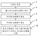
기판 제공, 기판 위에 단일 불소계 사진 패터닝층 증착, 기판 위에 첫 번째 및 두 번째 활성층 형성, 첫 번째 활성층 형성을 위한 사진 패터닝층의 형성 및 두 번째 활성층에 다른 사진 패터닝층 형성을 포함한 장치 제작 방법이다. 제안된 방법으로 밝혀진 실례들은 OLED 장치나 TFT 장치들의 포토 리소그래피의 단계 수를 줄인 것을 비롯하여 박막형 전자장치 형성에 사용될 수 있다.A method of fabricating a device comprising providing a substrate, depositing a single fluorine-based photo patterning layer on the substrate, forming first and second active layers on the substrate, forming a photo patterning layer for forming the first active layer, and forming another photo patterning layer on the second active layer. The examples identified by the proposed method can be used to form thin-film electronic devices, including reducing the number of steps in photolithography of OLED devices or TFT devices.
Description
본 발명은 하나의 포토리소그래피 단계로 두 개의 서로 다른 패턴이 두 개 이상의 서로 다른 활성층에 형성되도록 박막 장치에서 활성층을 패터닝하는 방법을 제공한다. 이 공정은 다층 패턴 유기 또는 무기장치를 형성하는 데 사용될 수 있다.The present invention provides a method of patterning an active layer in a thin film device such that two different patterns are formed in two or more different active layers in one photolithography step. This process can be used to form multilayer pattern organic or inorganic devices.
기판 위에 특성이나 구조에 맞게 놓인 패턴 유기재료를 사용하는 여러 가지 장치들이 알려져 있다. 유기재료는 일반적으로 무기재료보다 비용이 낮은 것이 특징이며 이러한 유기재료들은 큰 기판 위에서 재빨리 블랭키트 코팅을 씌워 크고 가격이 저렴한 장치를 형성할 수 있게 하여 흔히 원가 절감 가능성이 있는 것으로 간주되고 있다. 이러한 장치의 예를 들면 유기발광 2극장치(OLED)를 사용하는 디스플레이가 있다. 원가 절감 가능성 외에 이러한 디스플레이들은 대부분의 경쟁적인 디스플레이 기술보다 훨씬 더 효율적으로 발광하며 보다 뛰어난 화질을 보장할 수 있다. 그러므로 OLED 디스플레이는 대다수 시장에서 LCD 및 플라즈마 디스플레이를 대신할 수 있다. 이 OLED 기술은 또한 색상 조절용 등을 비롯한 다른 장치들에도 이용할 수 있다. 유기 반도체를 이용하여 유사한 장치 구조로 유기 박막 트랜지스터(oTFT)와 같은 유기 태양 장치, 유기 메모리 장치, 유기 전기부품 등을 형성할 수 있다.Various devices are known using patterned organic materials placed on a substrate to suit their properties or structure. Organic materials are generally characterized by lower cost than inorganic materials, and these organic materials are often considered to have potential cost savings by quickly blanking a large coating onto a large substrate to form a large and inexpensive device. An example of such a device is a display using an organic light emitting dipole (OLED). In addition to the potential for cost savings, these displays emit much more efficiently than most competitive display technologies and can guarantee better image quality. Therefore, OLED displays can replace LCD and plasma displays in most markets. The OLED technology can also be used in other devices, including for color control. The organic semiconductor may be used to form an organic solar device such as an organic thin film transistor (oTFT), an organic memory device, an organic electric component, or the like in a similar device structure.
유감스럽게도 OLED 기술 특히 OLED 디스플레이 기술 적용 속도는 느리다. 그 적용 속도가 이렇게 느린 것은 적어도 부분적으로는 이러한 재료들을 패터닝하여 실제의 디스플레이를 제작하는 데 소요되는 원가가 높기 때문이다. 유기재료를 패터닝하여 총 천연색 OLED 디스플레이를 만드는 여러 가지 방법이 시도되어 왔다. 섀도 마스크를 통하여 유기재료를 증착시킴으로써 여러 가지 색의 재료를 패터닝하는 것이 효과적임이 알려졌다. 그러나 이러한 섀도 마스크는 디스플레이의 해상도와 원만하게 코팅할 수 있는 기판의 크기를 제한하며 공정 시간을 증대시킨다. 컬러 방사체를 패터닝하는 데 레이저 증착을 이용하는 것과 같은 다른 방법들도 나왔지만 이러한 기술로는 흔히 디스플레이의 수율이 낮으며 또한 상당한 잔류 폐기물이 생성된다. 여러 가지 색의 유기 방사체의 용액 인쇄도 논의되어 왔으나 이러한 방법은 특징적으로 증착법으로 증착시킨 방사체에 비하여 발광 효율이 상당히 낮은 방사체를 만들게 된다. 이러한 낮은 효율은 접촉 저항이 커지기 때문이며 자주 쓰이는 중합체 재료가 흔히 소분자 재료보다 발광 효율이 낮고 수명이 짧으며 용액 증착의 이용으로 유기층을 통하여 수송체의 움직임을 조절하기 위하여 서로의 위에 증착시킬 수 있는 층의 수를 제한한다는 사실에 기인한다. 여러 색의 OLED 장치를 형성하기 위하여 패터닝한 컬러 필터와 함께 흰색 방사체를 사용하는 것을 비롯한 다른 방법들도 시도되어 왔다. 그러나 이러한 방법들도 OLED 디스플레이 내부에서 방사체의 효율성을 저하시킨다. oTFT등의 다른 유기 장치들은 유사한 패터닝 문제들에 처한다.Unfortunately, the application of OLED technology, especially OLED display technology, is slow. This slow application rate is due, at least in part, to the high cost of patterning these materials to produce the actual display. Several methods have been tried to pattern organic materials by patterning organic materials. It has been found effective to pattern materials of various colors by depositing organic materials through shadow masks. However, these shadow masks limit the resolution of the display and the size of the substrate that can be smoothly coated and increase process time. Other methods, such as using laser deposition to pattern color emitters, have also emerged, but these techniques often yield low displays and produce significant residual waste. Solution printing of organic emitters of various colors has also been discussed, but this method produces emitters with a significantly lower luminous efficiency than those deposited by vapor deposition. These low efficiencies are due to the increased contact resistance and commonly used polymer materials often have lower luminous efficiency and shorter lifetimes than small molecule materials and can be deposited on top of each other to control the movement of the carrier through the organic layer through the use of solution deposition. This is due to the fact that it limits the number of. Other methods have also been attempted, including the use of white emitters with patterned color filters to form multicolor OLED devices. However, these methods also reduce the efficiency of the emitter inside the OLED display. Other organic devices, such as oTFTs, face similar patterning problems.
유기재료의 세밀한 패터닝을 피하는 한 가지 방법은 하나의 층 또는 블랭키트 코팅층들을 포함하고 있는 OLED 디스플레이 구조를 적용하는 것이다. 예를 들어 Miller와 그의 동료들은 2006년11월26일에 발표한 “OLED 디스플레이”라는 제목의 미국 특허 7,142,179에서, 그리고 Cok와 그의 동료들은 2007년7월31일에 발표한 “OLED 장치”라는 제목의 미국 특허 7,250,722에서 각각 첫 번째와 두 번째의 패턴 전극 사이에 구성된 첫 번째 OLED 그리고 두 번째의 패턴전극과 블랭키트 코팅 전극 사이에 구성된 두 번째 OLED를 가지고 있는 구조에 대하여 논의하고있다. 이 문헌들에 따르면 첫 번째 OLED는 두 번째의 패턴전극이 기판에 연결되도록 패터닝되어야 한다. 또한 두 번째 전극은 OLED위에 증착된 후에 패터닝되어야 한다. 이러한 구조는 적어도 유기 재료층의 하나를 패터닝하지 않고도 보다 높은 효율의 광출력을 만들어 낸다. 그러나 이러한 구조들은 유기층 위에 전도층을 패터닝할 뿐 아니라 유기재료를 통하여 정공을 형성하기 위하여 유기층을 통과하는 매우 작은 구조를 패터닝할 것을 요한다. 고속 생산 환경에서 유기층 위에 이러한 길을 제공하고 전극 패턴을 형성하는 강력한 공정은 아직 기술적으로 알려지지 않고 있으며 따라서 이러한 장치 구조는 아직 성공적으로 제조되고 있지 않다. 이와 유사한 구조들은 또한 다층 태양전지와 기타 유기장치들을 구성하는 데도 바람직하다.One way to avoid fine patterning of organic materials is to apply OLED display structures comprising one layer or blank kit coating layers. For example, Miller and his colleagues in U.S. Patent 7,142,179 entitled "OLED Display" published November 26, 2006, and Cok and his colleagues published "OLED Device" published July 31, 2007. U.S. Patent 7,250,722 discusses a structure having a first OLED constructed between a first and a second pattern electrode and a second OLED constructed between a second pattern electrode and a blank kit coated electrode. According to these documents, the first OLED must be patterned so that the second pattern electrode is connected to the substrate. The second electrode must also be patterned after it is deposited over the OLED. This structure produces higher efficiency light output without patterning at least one of the organic material layers. However, these structures require not only to pattern the conductive layer over the organic layer but also to pattern very small structures passing through the organic layer to form holes through the organic material. The powerful process of providing this path over the organic layer and forming the electrode pattern in a high speed production environment is not yet technically known and therefore such device structures have not yet been successfully manufactured. Similar structures are also desirable for constructing multilayer solar cells and other organic devices.
무기 전자장치에서는 전기 요소들의 배열을 형성하기 위하여 큰 기판 위에 무기 반도체의 복합 박막층과 고해상도의 무기 전도층을 패터닝하는 데 포토리소그래피기술을 적용하는 것이 알려져있다. 유감스럽게도 이러한 장치들을 형성하기 위해 적용되는 포토리소그래피재료 및 용매는 유기재료를 분해하는 것으로 알려져있다. 그러므로 유기재료층 특히 활성 반도체 유기재료를 포함하고 있는 층이나 혹은 유기재료 위에 형성되는 층들을 패터닝하기 위하여 무기 고체회로를 만드는 데 쓰이는 것으로 알려져 있는 포토리소그래피재료와 용매를 적용하는 것은 불가능하다. In inorganic electronics, it is known to apply photolithography techniques to pattern a composite thin film layer of an inorganic semiconductor and a high-resolution inorganic conductive layer on a large substrate to form an array of electrical elements. Unfortunately, the photolithographic materials and solvents applied to form these devices are known to degrade organic materials. Therefore, it is not possible to apply solvents and photolithography materials known to be used to make inorganic solid circuits for patterning organic material layers, especially those containing active semiconductor organic materials, or layers formed on organic materials.
최근에 중합체 유기 반도체층을 패터닝하는 데서 포토리소그래피기술의 이용을 촉진하기 위하여 포토 레지스트 재료 및 용매가 기술적으로 논의되고있다. 예를 들어 Zakhidov와 그의 동료들은 2008년에 “고급 소재”3481-3484페이지에 “유기 전자재료의 화학적 처리를 위한 직교 배열용매로서의 불화수소 에테르”라는 제목으로 발표된 기사에서 불소계 감광성 수지가 감광성 수지 부분을 교차 결합하는 에너지원에 선택적으로 놓이는 상태에서 기판 위에 증착되고 감광성 수지가 패턴을 현상시키고 교차 결합이 되지 않은 감광성 수지 재료 부분을 제거하는 불화수소 에테르를 포함하고 있는 용매 안에서 현상되는 중합체 유기재료를 패터닝하는 방법에 대하여 논하고 있다. 불화수소 에테르 안에서 교차 결합된 감광성 수지의 용해도는 그 후 다른 용매의 사용을 통하여 재확인되었다. 그 다음에 활성 유기 반도체가 남아있는 감광성 수지 위에 증착되었 으며 남아있는 감광성 수지는 활성 유기 반도체를 패터닝하기 위하여 리프트오프하였다. 이와 같이하여 이 논문에서는 기판 위에 단일하고 용액 코팅된 중합 유기 반도체를 패터닝하는 것을 보여준다. 이와 같은 전반적 공정이 Lee와 그의 동료들에 의하여 2008년도의 “미국화학협회저널” 11564-11565페이지에 “산반응성 Semiperfluoroalkyl Resorcinarene:유기 전자공학을 위한 영상재료”라는 제목으로 발표된 기사에서 논의되고있다. Recently, photoresist materials and solvents have been technically discussed to facilitate the use of photolithography techniques in patterning polymeric organic semiconductor layers. For example, Zakhidov and his colleagues described a fluorine-based photosensitive resin in a article published in 2008 under “Advanced Materials” on pages 381-3484, “Hydrogen Fluoride Ether as Orthogonal Array Solvent for Chemical Treatment of Organic Electronic Materials”. Polymeric organic material deposited on a substrate with a selectively placed on an energy source that cross-links the portion, and developed in a solvent containing hydrogen fluoride ether, which photoresist develops the pattern and removes the non-cross-linked photosensitive resin material portion. How to pattern them. The solubility of the crosslinked photosensitive resin in the hydrogen fluoride ether was then reconfirmed through the use of other solvents. An active organic semiconductor was then deposited over the remaining photosensitive resin and the remaining photosensitive resin was lifted off to pattern the active organic semiconductor. As such, this paper demonstrates the patterning of a single, solution-coated polymeric organic semiconductor on a substrate. This general process is discussed in the article published by Lee and his colleagues in the 2008 American Chemical Society Journal on pages 11564-11565 entitled “Acid-reactive Semiperfluoroalkyl Resorcinarene: Imaging Materials for Organic Electronics”. .
Taylor와 그의 동료들은 2009년3월19일의 “고급소재” 2314-2317페이지에 “불화수소 에테르 용매를 사용하는 유기 전자공학을 위한 PSS:PEDOT의 직교 배열 패터닝”이라는 제목으로 발표한 기사에서 중합 유기 전도체(즉 PEDOT:PSS)가 기판 위에 형성되고 전도체 위에 감광성 수지가 형성되고 패터닝되며 전도체가 부식되고 유기 반도체(즉 Pentacene)가 적용되고 패터닝 되기 전에 두 번째 감광성 수지가 적용되고 패터닝되는 바닥 접촉 박막 트랜지스터의 형성에 대하여 논하고 있다. Taylor and his colleagues polymerized in an article published on March 19, 2009 titled “Orthogonal Array Patterning of PSS: PEDOT for Organic Electronics Using Hydrogen Fluoride Ether Solvents,” pages 2314-2317. An organic conductor (i.e., PEDOT: PSS) is formed on the substrate, a photosensitive resin is formed and patterned on the conductor, a bottom contact thin film in which a second photosensitive resin is applied and patterned before the conductor is corroded and the organic semiconductor (i.e., Pentacene) is applied and patterned. The formation of transistors is discussed.
이러한 논문들은 각각 전기회로에서 요소들을 만들어 내기 위하여 개량된 리소그래피 공정과 재료들을 사용하는 용액 코팅 중합체 유기재료의 패터닝과 OLED 장치에 아직 적용되어 있지 않은 공정과 재료들의 사용에 대하여 논하고있다. 또한 이 논문들은 중합체를 사용하는 이러한 재료와 공정들의 적용에 대하여 논하면서 소분자 유기재료의 층들을 패터닝하는 방법에 대해서는 언급하지 않고 있다. 또한 이 방법에 따른다면 적어도 하나의 유기층을 포함한 여러 층들과 전기 전도체와 같은 이 유기층 위에 증착된 층에 패턴을 만들기 위하여 여러 사진 패터닝 단계, 특히 각 패턴층에 대하여 하나의 사진 패터닝 단계를 수행할 필요가 있다. 사진 패터닝 단계를 수행하기 위하여 포토리소그래피재료를 복사선에 노출시키는 것과 같은 어떤 포토리소그래피 공정 단계는 공기 중에서 진행되는 것이 특징이다. 유감스럽게도 공기 중에는 유기재료가 반응할 수 있는 산소와 습기가 있다. 그러므로 그 일부는 유기층 위에서 형성되는 사진 패터닝 재료의 여러 층을 형성함으로써 유기장치의 다층 사진 패터닝을 수행하는 것은 장치의 성능을 낮추는 결과를 초래할 수 있다. 또한 이러한 각 포토리소그래피 단계는 수행하는 비용이 많이 들며 사진 패터닝 재료의 증착뿐 아니라 장치 안의 각 층에서의 패턴의 노출, 현상, 리프트오프와 같은 하나의 완전한 포토리소그래피 단계를 요구한다.Each of these papers discusses the patterning of solution-coated polymer organic materials using advanced lithography processes and materials to create elements in electrical circuits, and the use of processes and materials not yet applied in OLED devices. The papers also discuss the application of these materials and processes using polymers and do not mention how to pattern layers of small molecule organic materials. The method also requires several photo patterning steps, in particular one photo patterning step for each pattern layer, to pattern the layers deposited on the organic layers, such as at least one organic layer and the electrical conductors. There is. Certain photolithographic processing steps, such as exposing the photolithographic material to radiation to perform the photo patterning step, are characterized by running in air. Unfortunately, there is oxygen and moisture in the air where organic materials can react. Therefore, performing multilayer photo patterning of the organic device by forming several layers of photo patterning material, some of which are formed on the organic layer, may result in lowering device performance. In addition, each of these photolithography steps is expensive to perform and requires one complete photolithography step, such as the deposition of photo patterning material, as well as the exposure, development, and liftoff of the pattern in each layer within the device.
다른 방법으로서 Katz와 Dhar는 2009년4월10일에 제출된 “불소계 화합물을 이용하는 패터닝 장치”라는 제목의 국제 공개 번호 WO2009/126916에서 기판 위에서 패터닝될 활성층의 형성, 불소층에서 사진 패터닝 재료에 대한 복사선 노출에 대하여 논하고 있다. 그러나 이 방법은 하나의 활성층을 패터닝하는 데 여러 층의 증착을 요구한다.Alternatively, Katz and Dhar, in International Publication No. WO2009 / 126916, entitled “Pattern Using Fluorine-Based Compounds,” filed April 10, 2009, describe the formation of an active layer to be patterned on a substrate, for the photo patterning material in the fluorine layer. Radiation exposure is discussed. However, this method requires deposition of several layers to pattern one active layer.
또 다른 방법으로 Taussig와 그의 동료들은 2007년4월10일에 발표된 “하나 이상의 박막을 형성하는 방법”이라는 제목의 미국 특허 7,202,179에서 장치의 층들 위에서 3차원 구조를 부각하기 위해 3차원 탬플릿이 쓰이며 마감 구조를 만들기 위해 3차원 구조와 바탕층들이 부식되는 방법을 논하고 있다. 이 방법은 단일한 인쇄 리소그래피 단계를 이용하여 상이한 패턴이 장치의 상이한 층에 형성되도록 함으로써 여러 리소그래피 단계의 정렬이 필요없게 하며 따라서 이 방법을 안정하지 않은 기판, 예를 들면 제조과정에 확장되거나 수축되는 합성수지와 같은 기판 위에 장치를 형성하는 데 적용할 수있게 한다. 유감스럽게도 제공된 방법은 유기 반도체 재료와 호환되지 않는 재료와 방법을 적용하기 때문에 무기 구조에만 유용하다. 또한 이 방법은 현재 대량 생산에 사용되지 않는 기술을 적용하고 패터닝 단계가 요구되는 결과를 달성하도록 엄격한 공정 관리를 요구한다.Alternatively, Taussig and his colleagues used a three-dimensional template to highlight the three-dimensional structure on the layers of the device in US Patent 7,202,179, entitled "How to Form One or More Thin Films," published April 10, 2007. The three-dimensional structure and how the underlying layers are corroded are discussed to create a finished structure. This method uses a single print lithography step to allow different patterns to be formed on different layers of the device, eliminating the need for alignment of several lithography steps and thus extending or shrinking the process in an unstable substrate, for example, during manufacturing. It can be applied to form a device on a substrate such as a resin. Unfortunately, the provided methods are useful only for inorganic structures because they apply materials and methods that are incompatible with organic semiconductor materials. The method also requires strict process control to apply techniques that are not currently used in mass production and to achieve the results that require a patterning step.
그러므로 유기 재료층에서의 첫 번째 패턴의 형성과 적어도 유기층 위에 형성된 개별적 활성 재료층에서의 두 번째 다른 패턴의 형성을 허용하는 방법이 필요하게 된다. 이 공정은 강력해야 하고 미크론에 가까운 해상도에서 패턴의 형성을 허용해야 하며 유기재료가 현상되는 동안 공기 중에 노출되지 말아야 한다. 특히 이 방법이 증착된 소분자 유기재료와 호환할 수 있는 것이 바람직하다. 이상적으로 이와 같은 방법은 비유기 장치와도 호환할 수 있을 것이며 이러한 장치들 내부에서 여러 층이 단일한 포토리소그래피 단계에 응답하여 다르게 패터닝될 수 있게 될 것이다.Therefore, there is a need for a method that allows the formation of a first pattern in an organic material layer and at least a second different pattern in an individual active material layer formed over the organic layer. This process should be robust and allow for the formation of patterns at near micron resolution and should not be exposed to the air while the organic material is being developed. It is particularly desirable for this method to be compatible with the deposited small molecule organic material. Ideally, such a method would be compatible with inorganic devices, and multiple layers within these devices would be able to be patterned differently in response to a single photolithography step.
본 발명은 기판의 제공, 기판 위에서 단일한 불소계 사진 패터닝층의 증착, 기판위에서 첫 번째와 두 번째 활성층의 형성, 첫 번째 활성층안에서 첫 번째 패턴을 형성하고 두 번째 활성층안에서 두 번째의 다른 패턴을 형성하도록 사진 패터닝을 적용하는 것을 포함하는 장치를 형성하는 방법을 제공한다. 본 발명에서 제시된 특정한 실례들은 보다 적은 수의 포토리소그래피 단계를 가진 OLED 장치와 TFT를 비롯한 박막 전자장치를 형성하는 데 사용할 수 있다.The present invention provides a substrate, the deposition of a single fluorine-based photo patterning layer on the substrate, the formation of the first and second active layers on the substrate, the first pattern in the first active layer and the second other pattern in the second active layer. To provide a method of forming an apparatus comprising applying photo patterning to the. Certain examples presented in the present invention can be used to form thin film electronics, including TFTs, and OLED devices with fewer photolithography steps.
본 발명의 여러 측면을 통하여 장치 안에 있는 여러 층이 단일한 감광성 수지 재료층의 증착, 노출, 현상을 통하여 독특하게 패터닝될 수 있게 하는 이점이 제공된다. 이 공정은 유기 및 무기장치 어느 것에나 적용할 수 있으며 장치안에서 일부는 유기층으로 되어있는 여러 층의 패터닝을 가능하게 한다. 따라서 이 방법은 다층 유기장치가 제조과정에 장치를 비활성 환경에서 이동시키지 않고도 형성될 수 있게 하여 이전에 대량생산환경에서는 불가능하였던 고품질유기장치구조의 형성을 가능하게 한다. 장치의 층들의 많은것은 단일한 노출로 패터닝될 수 있기때문에 본 발명의 여러 측면을 통하여 불안정하고 유연한 기판 위에서도 박막장치의 제조를 가능하게 한다. 또한 이 방법은 고도의 병렬 따라서 신속한 공정으로 매우 높은 해상도(예를 들면 미크론 준위의 해상도)를 제공하는 것을 비롯하여 기존의 포토리소그래피 방법의 장점을 모두 가지고 있다. 또한 이 방법은 크게 전체 공정시간을 줄이고 제조과정에 감광성 수지 재료의 여러 층을 증착시키고 현상시켜야 할 필요성을 없애면서 장치가 보다 적은 포토리소그래피 단계로 수행될 수 있게 하고 따라서 제조원가를 크게 절감시켜 준다.Various aspects of the present invention provide the advantage that multiple layers in the device can be uniquely patterned through deposition, exposure, and development of a single layer of photosensitive resin material. This process can be applied to both organic and inorganic devices and allows the patterning of several layers, some of which are organic layers in the device. This method thus allows multilayer organic devices to be formed during manufacturing without moving the devices from the inert environment, thus enabling the formation of high quality organic device structures that were previously impossible in mass production environments. Many of the layers of the device can be patterned with a single exposure, thus allowing the fabrication of thin film devices on unstable and flexible substrates through various aspects of the present invention. The method also has all the advantages of conventional photolithography methods, including very high resolution (eg micron resolution) in a highly parallel and rapid process. This method also significantly reduces the overall process time and eliminates the need to deposit and develop multiple layers of photosensitive resin material in the manufacturing process, allowing the device to be performed in fewer photolithography steps and thus significantly reducing manufacturing costs.
그림 1. 본 발명의 예시적인 방법의 단계를 보여주는 흐름도
그림 2. 본 발명을 구체화한 세부단계를 보여주는 흐름도
그림 3A-3I. OLED 디스플레이를 형성하기 위한 본 발명의 방법의 예제 단계를 보여주는 공정도
그림 4A-4L. TFT 배열을 형성하기 위한 본 발명의 방법의 예제 단계를 보여주는 공정도
그림 5. TFT배열을 형성하기 위한 본 발명의 방법의 예제 단계를 보여주는 흐름도.Figure 1. Flowchart showing the steps of an exemplary method of the present invention
Figure 2. Flowchart showing detailed steps embodying the present invention
Figure 3A-3I. Process diagram showing example steps of the method of the present invention for forming an OLED display
Figure 4A-4L. Process diagram showing example steps of the method of the present invention for forming a TFT array
Figure 5. Flow chart showing example steps of the method of the present invention for forming a TFT array.
현재의 발명 중에서 몇 가지 실시 예들이 상세하게 아래에 논의되고 있다. 실시 예들의 설명에서 명확성을 위해 특정한 용어를 사용한다. 그러나 본 발명이 선택된 특정한 전문 용어로 고의적으로 제한되게 하는 것은 아니다. 그 분야 기술자라면 다른 대등한 구성요소들을 사용할 수 있고 현행 발명의 넓은 개념에서 벗어나지 않고 다른 방법들이 개발될 수 있다는 것을 인식할 수 있다. Some embodiments of the present invention are discussed in detail below. Specific terminology is used in the description of the embodiments for clarity. However, it is not intended that the present invention be deliberately limited to the particular terminology selected. Those skilled in the art will recognize that other equivalent components may be used and other methods may be developed without departing from the broader spirit of the present invention.
본 발명의 윤곽은 그림1에서 보여준 것과 같은 박막장치를 형성하기 위한 방법을 제공한다. 본 발명의 특정한 실례들에 있는 박막장치들에는 무기 박막층들뿐만 아니라 유기 박막층들을 가지고 있는 장치들이 있다. 특히 중요하게는 본 발명의 윤곽이 기판 2의 제공, 그 기판 위에 불소계 사진 패터닝 단일층 4의 증착, 그 기판 위에 첫 번째와 두 번째 활성층 6, 8의 형성,그리고 첫 번째 활성층에 첫 번째 패턴을 형성하고 두 번째 활성층에 두 번째인 다른 패턴을 형성하기 위하여 사진 패터닝층 10의 적용을 포괄하는 장치를 형성하기 위한 방법을 제공한다. 서로 다른 패턴들이 첫 번째와 두 번째 층들에 제공될 수 있게 하기 위해서 사진 패터닝층을 복사선에 노출시켜 3개의 독특한 노출된 재료의 비중첩 패턴들을 생성하여 최종 장치 내에서 활성적 즉 기능적인 두 개의 재료층들을 증착하고 또한 그 두 개의 각 활성 재료층들에 서로 다른 패턴들을 나누어 주기 위해서 사진 패터닝층을 사용한다. 이러한 서로 다른 패턴들은 사진 패터닝층을 첫 번째 불소계 용매에 노출시켜 첫 번째 패턴을 현상하고 또한 적어도 두 번째 불소계 용매에 노출시켜 적어도 두 번째 패턴을 사진 패터닝층 내에 현상함으로써 2개의 활성 재료층들에 대체로 나누어 주게 된다. 사진 패터닝층은 리프트오프나 부식을 통해서 활성 재료층에 대체로 넘어가게 된다. 리프트오프를 적용할 때 그 공정 단계들은 그림 1에서 보여준 것처럼 정리될 수 있다. 그러나 이것은 필수가 아니다. 부식을 사용할 때 불소계 첨가형 사진 패터닝층4은 첫 번째와 두 번째 활성층들인 6, 8을 형성한 후에 증착될 수 있다. 본 발명에 따른다면 사진 패터닝층은 고도의 불소계 재료층을 포함할 수 있고 용매는 높은 불소계 용제들을 포함할 수 있다.The outline of the present invention provides a method for forming a thin film device as shown in FIG. Thin film devices in certain examples of the present invention include devices having organic thin film layers as well as inorganic thin film layers. Of particular importance is the contour of the present invention providing a
본 발명의 방법 중에서 일부 실시 예들은 발명가들에 의해 수행되었 고 두 가지 별도의 실험적인 관찰들에 의존하고 있다. 첫 번째로 발명가들은 불소계 사진 패터닝 단일층이 기판에 증착된 다음 불소계 사진 패터닝층의 상이한 부분들을 복사선의 양을 상이하게 하면서 그에 노출시키면 보다 적게 노출된 부분들은 보다 세게 노출된 부분들보다 많은 불소계 용제들에 의해서 제거될 수 있다는 것을 관찰하였다. 그러므로 이러한 상이한 부분들이 제거되는 시간들사이에서 추가적인 공정단계들을 완성할 수 있다면 노출을 조절하고 적절한 불소계용제들을 선택함으로써 불소계사진 패터닝층의 상이한 부분들을 상이한 시간에 제거할 수 있다. 두 번째로 발명가들은 불소계 사진 패터닝층과 종래의 비불소계 사진 패터닝층으로 된 이중층을 형성할 수 있으며 그 두 개의 층들이 화학반응을 일으키지 않고 또 두 층들의 노출을 서로 다르게 조절할 수 있다는 식으로 서로가 관계없이 일을 수행한다는 것을 관찰하였다. 더욱이 비불소계사진 패터닝층이 불소계 사진 패터닝층의 부분 위에서 제거될 때 불소계 사진 패터닝층이 노출된 부분은 비불소계 사진 패터닝층의 밑에 있는 불소계 사진 패터닝층보다 훨신 더 빨리 그리고 쉽게 리프트오프될 수 있다. 따라서 이중층을 사용하면 용제의 감도를 추가적으로 구별할 수 있어 또 다른 시간에 제거될 수 있는 다른 영역을 형성하는 능력을 제공할 수 있다. 또한 이러한 이중층의 사용은 또 다른 이점을 갖는데 그것은 비불소계 사진 패터닝층의 일부를 제거함으로써 노출된 불소계 사진 패터닝층 부분을 제거할 때 리프트오프를 적용하면 불소계 사진 패터닝층이 남아있는 부분에 대한 중요한 undercut profile로 끝날 수 있다는 것이다.Some embodiments of the method of the invention have been carried out by the inventors and rely on two separate experimental observations. Firstly, the inventors found that when a single layer of fluorine-based photo patterning was deposited on a substrate and then exposed different portions of the fluorine-based photo-patterning layer with different amounts of radiation, the less exposed portions were more fluorine-based than the more exposed portions. It has been observed that they can be removed by them. Therefore, if additional process steps can be completed between times at which these different portions are removed, different portions of the fluorine-based patterning layer can be removed at different times by controlling exposure and selecting appropriate fluorine-based solvents. Secondly, the inventors can form a bilayer consisting of a fluorine-based photopatterning layer and a conventional non-fluorine-based photopatterning layer, in which the two layers can control the exposure of the two layers differently without causing a chemical reaction. Observed that the work is done regardless. Moreover, when the non-fluorine-based photo patterning layer is removed over a portion of the fluorine-based photo patterning layer, the exposed portion of the fluorine-based photo patterning layer can be lifted off much faster and easier than the fluorine-based photo patterning layer underneath the non-fluorine-based photo patterning layer. Thus, the use of bilayers can further distinguish the sensitivity of the solvent, providing the ability to form other areas that can be removed at another time. In addition, the use of such a bilayer has another advantage, which is an important undercut to the area where the fluorine-based photo patterning layer remains when liftoff is applied when removing the exposed portion of the fluorine-based photo patterning layer by removing part of the non-fluorine-based photo patterning layer. can end with a profile.
이러한 관측은 복합 박막 장치를 형성하기 위해 적용할 수 있는 새로운 방법을 생성하기 위해 사용할 수 있다. 예를 들어 본 발명의 방법의 특정한 예는 미국 특허7,142,179에서 Miller와 그의 동료들에 의해 논의된것과 같은OLED 장치 구조를 포함하여 특정한 OLED 장치 구조 형성에 특히 유익할 수 있다. 또한 그 방법들은 특정한 TFT구조들을 형성하는 데 유익할 수 있다. 그러한 장치들을 형성하기 위한 보다 상세한 실시 예들이 이번 발표에서 제공된다.These observations can be used to create new methods that can be applied to form composite thin film devices. For example, certain examples of the method of the present invention may be particularly beneficial for forming particular OLED device structures, including OLED device structures as discussed by Miller and colleagues in US Pat. No. 7,142,179. The methods may also be beneficial for forming certain TFT structures. More detailed embodiments for forming such devices are provided in this announcement.
본 발명의 방법의 특정한 실례들을 명확하고 간결하게 발표하기 위하여 이번 발표에서 사용되는 특정한 용어를 결정하는 것이 중요하다. 본 발명에서 “유기장치”는 유기분자들을(즉 수소원자와 탄소원자를 함유하고 있는 분자) 포함하는 활성층이 들어있는 장치이다. 특정한 실시 예에서 이러한 유기분자들은 Alq와 같은 유기반도체들이거나 pentacene과 같은 전도체들이다. 반대로 “무기장치”는 유기분자를 포함하는 활성층이 전혀 없는 장치이다. “활성층”은 구성되고 있는 장치에서 기능적인 층이다. 본 발명의 특정한 측면에 의해 대상으로 정해진것과 같은 박막전자장치에서 흔히 활성층들은 반도체나 전도체를 포함할 수 있을 뿐만 아니라 절연체도 포함할 수 있다. 활성층은 단일 균질층일 수 있지만 장치 내에서 기능층을 함께 형성하는 여러 박막층들을 번갈아 포함할 수 있다. 예를 들어 OLED에서 활성층은 흔히 구멍 전송이나 전자 수송층을 비롯해서 2 극장치 속에 각 유기층을 포함할 수 있다. 이러한 층들이나 별도의 중간 박막층 중의 하나가 더욱 나아가서는 빛을 발광한다. 본 발명의 특정한 측면과 관련해서 유기재료들을 특별히 주의해서 다룰 필요가 있을 수 있다. 일부 유기 반도체들의 성능은 공기나 습기에 노출됨으로써 크게 저하될 수 있다. 더욱이 대부분의 유기재료들은 기존의 포토리소그래피에서 사용되는 비불소계 용매들에서 잘 용해되므로 유기재료들을 증착시킨 후에 이러한 용매를 장치에 사용하는 것은 바람직하지 않다. 그러나 유기재료들은 대체로 높은 불소계 용매에서 용해되지 않으므로 유기재료들이 장치에 증착된 후에 이러한 용매들을 사용할 수 있다.It is important to determine the specific terminology used in this presentation in order to present specific examples of the method of the invention in a clear and concise manner. In the present invention, an "organic device" is a device containing an active layer containing organic molecules (ie, molecules containing hydrogen atoms and carbon atoms). In certain embodiments, these organic molecules are organic semiconductors such as Alq or conductors such as pentacene. In contrast, an "inorganic device" is a device without any active layer containing organic molecules. The "active layer" is the functional layer in the device being constructed. In thin film electronic devices such as those targeted by certain aspects of the present invention, the active layers may include not only semiconductors or conductors, but also insulators. The active layer may be a single homogeneous layer but may alternately comprise several thin layers that together form a functional layer in the device. In OLEDs, for example, the active layer can often contain each organic layer in two theaters, including a hole transport or electron transport layer. One of these layers or a separate intermediate thin film layer further emits light. It may be necessary to pay special attention to organic materials in connection with certain aspects of the present invention. The performance of some organic semiconductors can be greatly degraded by exposure to air or moisture. Moreover, since most organic materials dissolve well in the non-fluorine solvents used in conventional photolithography, it is not preferable to use such a solvent in the apparatus after the organic materials are deposited. However, organic materials generally do not dissolve in high fluorine-based solvents so that these solvents can be used after organic materials are deposited in the device.
본 발명의 방법의 특정한 실시 예들은 “박막”장치들에 적용할 수 있다. 이러한 장치들은 대체로 두께가 200nm미만의 층을 포함하며 때때로 두께가 50nm미만의 층을 포함한다. 박막장치들의 층들은 흔히 증발, 스퍼터링 또는 용액 코팅과 같은 기술들을 이용하여 증착된다. 이러한 장치들은 대체로 장치의 박막층들이 박리되지 않도록 하기 위해서 구조를 흠없이 완전하게 해주는 지지물인 “기판” 위에 형성된다. “기판”이라는 용어는 구조를 흠없이 완전하게 해주기 위해서 코팅될 수 있는 박막층 위의 모든 지지물을 가리킨다. 기술 분야에서 알려진 기판들에는 대표적으로 유리로 형성된 딱딱한 기판과, 대표적으로 불수 강박판이나 합성수지로 형성되는 유연한 기판들이 있다. 기판은 또한 습기나 산소로부터 모든 유기재료를 보호하는 환경 장벽의 일부를 제공할 수 있지만 여기서는 필요로 하지 않는다. 기판은 불투명, 투명 혹은 반투명일 수 있다. 기판은 더 나아가서 장치에 전기를 전도하기 위해 금속 모선이나 무기 반도체 재료와 같이 하나 또는 그 이상의 층들을 포함할 수 있다. 기판은 활성층들을 기판이나 기판의 전도성 요소로부터 절연하는 것과 같은 기능들을 수행하기 위해서 유기재료의 비전도층들을 포함할 수 있다. 비전도성 유기층들이 기판의 일부로 포함될 수도 있는데 그때는 이러한 층들이 기판의 겉면을 매끄럽게 해줌으로써 형성된 박막층들이 균일한 층으로 될 수 있게 한다.Certain embodiments of the method of the present invention are applicable to "thin film" devices. Such devices typically include layers less than 200 nm thick and sometimes less than 50 nm thick. Layers of thin film devices are often deposited using techniques such as evaporation, sputtering or solution coating. These devices are usually formed on a "substrate" which is a support that completes the structure flawlessly to prevent the thin layers of the device from peeling off. The term "substrate" refers to any support on a thin film layer that can be coated to complete the structure flawlessly. Substrates known in the art include rigid substrates typically formed of glass and flexible substrates typically formed of inert steel foils or synthetic resins. The substrate may also provide part of an environmental barrier that protects all organic materials from moisture or oxygen but is not required here. The substrate may be opaque, transparent or translucent. The substrate may further comprise one or more layers, such as a metal bus bar or an inorganic semiconductor material, to further conduct electricity to the device. The substrate may include nonconductive layers of organic material to perform functions such as insulating the active layers from the substrate or conductive elements of the substrate. Non-conductive organic layers may also be included as part of the substrate, which then smoothes the outer surface of the substrate so that the formed thin layers can be uniform.
본 발명에서 사용한“부식”이라는 용어는 사진 패터닝층의 나머지 부분이나 일부가 활성층의 기본 영역을 노출로부터 제거공정까지 보호하는 데 쓰이는 공정을 말한다. 예를 들어 사진 패터닝층의 나머지 부분들은 활성 유기층의 비보호 부분들을 증발시켜, 기판으로부터 그것들을 제거하는 플라즈마 스트림에서부터 활성층의 부분들을 보호할 수 있다. 여러 가지 화학공정들과 부식공정들은 이 기술분야에서 알려진 상이한 재료들을 제거하는 데 사용될 수 있으며 부식법들은 특정한 첫 번째 재료에 대한 효과가 크도록 선택되거나 조절될 수 있는 한편 다른 두 번째 재료에 대한 효과는 미미하거나 전혀 없어야 한다. “리프트오프”라는 용어는 활성층을 사진 패터닝층의 부분 위에 증착시키고 그 기판을 사진 패터닝층 부분을 제거하는 용매에 노출시키는 데 그 때 그 활성층의 덧놓인 부분이 제거되는 그러한 과정을 말한다.The term “corrosion” used in the present invention refers to a process in which the rest or part of the photo patterning layer is used to protect the basic area of the active layer from exposure to removal. For example, the remaining portions of the photo patterning layer may evaporate the unprotected portions of the active organic layer to protect portions of the active layer from the plasma stream that removes them from the substrate. Various chemical processes and corrosion processes can be used to remove different materials known in the art and corrosion methods can be selected or adjusted to have a greater effect on the particular first material, while on other second materials. Must be insignificant or absent at all. The term "liftoff" refers to such a process in which the active layer is deposited over a portion of the photo patterning layer and the substrate is exposed to a solvent that removes the portion of the photo patterning layer, wherein the overlay of the active layer is removed.
사진 패터닝층을 참조할 때 본 발명에서 사용한“패턴”이라는 용어는 물리적 특성이나 화학적 특성에서 사진 패터닝층의 다른 부분들과 차이 나는 사진 패터닝층의 공간 배열을 나타낸다. 그러나 활성층에 적용할 때 용어“패턴”은 보다 정확하게 말한다면 특정한 패턴대로 활성층의 해당 부분을 제거해서 만드는 데 두께가 변하는 층과 이상적으로는 일부 물리적인 위치에서는 존재하나 다른 물리적 위치에서는 존재하지 않는 층이 만들어지는 실제적인 패턴을 말한다. 즉 활성층에 적용할 때“패턴”이라는 용어는 기판의 특정 영역에 있는 활성층의 첫 번째 부분을 실제적으로 제거하는 한편 기판의 또 다른 영역에 활성층의 두 번째 부분을 실제적으로 재치있게 남겨두는 식으로 만들어지는 공간적 배열을 말한다.The term “pattern” used in the present invention when referring to a photo patterning layer refers to a spatial arrangement of the photo patterning layer that differs from other parts of the photo patterning layer in physical or chemical properties. However, when applied to an active layer, the term “pattern” more precisely refers to a layer of varying thickness, ideally in some physical locations but not in other physical locations, as a specific pattern removes that portion of the active layer. This refers to the actual pattern that is created. In other words, when applied to an active layer, the term “pattern” is used to actually remove the first part of the active layer in a particular area of the substrate, while leaving the second part of the active layer really clever in another area of the substrate. Losing is a spatial arrangement.
“노출”이라는 용어는 이 문서에서 두 개의 다른 문맥으로, 즉 용매에 대한 노출 혹은 복사선에 대한 노출로 사용되고 있다. 용매에 대한 노출은 대체로 용매에 담그기, 용매 안에서의 전체 기판의 동시적이고 균일한 코팅을 포함하고 있다. 그러나“노출”이라는 용어는 복사선에 적용할 때 복사선의 선량이나 노출 정도가 조절되고 대체로 기판상에서 변하며 결과 어떤 영역들은 다른 영역들보다 더 많은 복사선량을 받는 그러한 과정에 적용된다. 이것은 여러 방법들 중 임의의 것에 의해서 이루어 지는데 그러한 예를 든다면 상이한 마스크들에 의한 다중노출에 대한 기판의 노출, 상이한 장소에서 상이한 양의 빛을 투과시키는 흑백 포토마스크를 통한 기판의 노출, 세기나 지속 시간이 변하는 레이저 패터닝을 통한 방법 또는 홀로그램 방법을 사용한 레이저 노출에 의한 기판의 노출이 포함되는데 홀로그램 방법에 의하면 패턴의 전체 혹은 (보다 좋은 것은) 하나의 요소가 적절한 양의 빛을 수용하는 그 패턴 내의 모든 상이한 영역들과 함께 노출된다. 여기서 마지막 방법은 백플레인 트렌지스터와 같은 반복되는 요소들을 형성할 때 롤-투-롤 형식에서의 레이저 패터닝과 결합될 수 있다. 즉 레이저는 기판에 다중 노출 영역을 갖는 패턴을 생성하기 위하여 홀로그램 박막을 통해서 상을 그릴 수 있는 반면 레이저는 기판에 대하여 고정된 위치에서 상을 그리게 되며 하나 또는 더 이상의 요소들의 상을 그릴 수 있는데(즉 TFT나 OLED픽셀), 그 때 레이저를 기판에서 다른 위치로 옮길 수 있으며 또 다른 요소나 요소 그룹의 상을 그리는 데 이용할 수 있다. 이 때 OLED응용 분야에서 비아홀과 주변의 각 요소의 영역이 제한된다.The term "exposure" is used in this document in two different contexts: exposure to solvents or exposure to radiation. Exposure to the solvent usually involves immersion in the solvent, simultaneous and uniform coating of the entire substrate in the solvent. However, the term “exposure” applies to such processes where, when applied to radiation, the dose or exposure of the radiation is controlled and usually varies on the substrate, with some regions receiving more radiation than others. This is accomplished by any of several methods, such as the exposure of the substrate to multiple exposures by different masks, the exposure of the substrate through a black and white photomask that transmits different amounts of light at different places, the intensity or Exposure of the substrate by laser patterning using a method of laser patterning or a method of varying duration, according to the hologram method, is a pattern in which the whole or (and better) one element receives an appropriate amount of light. It is exposed with all the different areas in it. The final method here can be combined with laser patterning in a roll-to-roll format when forming repeating elements such as backplane transistors. That is, a laser can draw an image through a holographic thin film to create a pattern with multiple exposure areas on a substrate, while a laser can draw an image at a fixed position relative to the substrate and can draw an image of one or more elements ( TFT or OLED pixels), then the laser can be moved to another position on the substrate and used to draw another element or group of elements. In this case, the area of each element around the via hole and the surrounding area is limited.
“전극”이라는 용어는 장치의 박막층들 내에 전기장을 생성할 능력이 있는 하나의 전도층을 기능적으로 제공하는 층 혹은 복합 박막층들의 결합을 의미한다. 전극은 투명, 반투명 혹은 불투명일 수 있다. 그러나 본 발명의 OLED 장치들에서 첫 번째 와 두 번째 전극들 중 적어도 하나는 투명이거나 반투명일 수 있다. 본 발명의 특정한 실시 예들에서 장치 내 첫 번째 ,두 번째 전극들 중 하나는 흔히 불투명하고 반사적일 수 있다. 본 발명의 특정한 실시 예들에서 유용한 대표적인 전극들은 두께가 10-30nm사이이다. 본 발명의 특정한 실시 예들에서 장치들의 박막층에 전기장을 생성하기 위해서 전극들은 전기를 전도할 수 있는 유기재료나 무기재료로 형성할 수 있다. 전극을 형성하는 데 유용한 대표적인 무기재료들로는 인디움 석산화물이나 인디움 아연산화물과 같은 특정한 혼합물을 생성하는 금속 산화물뿐만 아니라 은, 금, 백금, 구리, 몰리브덴 및 알루미늄과 같은 금속들이 있다. 전극들은 전극 인쇄나 스퍼터링을 비롯한 다양한 방법들을 써서 형성될 수 있다. 그러나 특정한 실시 예들에서는 증발이나 시선 증착을 제공하는 다른 방법들을 써서 전극을 형성하기 위하여 무기재료들을 증착하는 것이 바람직하다. 전극을 형성하는 데 쓸모있는 유기재료들로는 PEDOT/PSS와 같은 고도로 정돈된 공중합체들이 있다. 전극은 인쇄법을 비롯한 많은 방법들을 이용해서 형성될 수 있다. 그러나 증착속도를 높이고 공정시간을 줄이기 위하여 전극들을 형성하는 데 쓰이는 재료 특히 두 번째 전극을 형성하기 위해서 쓰이는 재료는 기판 위에 박막을 형성해주는 층코팅법을 써서 증착되는 것이 더 나은 것으로 여겨진다.The term “electrode” refers to a combination of layers or composite thin layers that functionally provides one conductive layer capable of generating an electric field in the thin layers of the device. The electrode can be transparent, translucent or opaque. However, at least one of the first and second electrodes in the OLED devices of the present invention may be transparent or translucent. In certain embodiments of the present invention, one of the first and second electrodes in the device can often be opaque and reflective. Representative electrodes useful in certain embodiments of the present invention are between 10-30 nm thick. In certain embodiments of the present invention, the electrodes may be formed of an organic or inorganic material capable of conducting electricity in order to generate an electric field in the thin film layer of the devices. Representative inorganic materials useful for forming electrodes include metals such as silver, gold, platinum, copper, molybdenum and aluminum, as well as metal oxides that produce specific mixtures such as indium oxide or indium zinc oxide. Electrodes can be formed using a variety of methods, including electrode printing or sputtering. However, in certain embodiments, it is desirable to deposit inorganic materials to form the electrode using other methods of providing evaporation or eye deposition. Organic materials useful for forming electrodes include highly ordered copolymers such as PEDOT / PSS. The electrode can be formed using a number of methods including printing. However, the material used to form the electrodes to increase the deposition rate and the process time, in particular the material used to form the second electrode, is considered to be better deposited using a layer coating method to form a thin film on the substrate.
“패턴 전극”이라는 용어는 보다 정확하게 말하자면 기판에 걸쳐 분할되고 있는 전극들을 의미하는 것으로서 전극의 각 세그먼트는 한 개 또는 많은 전기적 구성 요소나 발광장치들에 의해서 공유되지만 기판의 모든 전기적 구성 요소들이나 발광 요소들이 똑같은 전극의 세그먼트를 공유하지 않는다. 즉 전극의 임의의 두 세그먼트를 통하는 전류의 흐름은 독립적으로 조절할 수 있어서 각 세그먼트와 접촉하고 있는 전기적 구성 요소나 발광 요소를 통하는 전류의 흐름을 개별적으로 조절한다.The term “pattern electrode”, more precisely, refers to electrodes that are divided across a substrate, where each segment of the electrode is shared by one or many electrical components or light emitting devices, but all electrical components or light emitting elements of the substrate. They do not share the same segment of the electrode. That is, the flow of current through any two segments of the electrode can be independently controlled to individually regulate the flow of current through the electrical component or light emitting element in contact with each segment.
“불소계 사진 패터닝층”을 형성하는 데 사용되는 불소계 감광성 수지 재료는 resourcinarene, perfluorodecyl methacrylate의 공중합체 그리고 2-nitrobenzyl methacrylate, 그 유도체나 다른 공중합 감광성 수지 혹은 hydrofluorether로 형성되는 용매와 같은 불소계 용매에서 감광성 수지를 녹이기에 충분한 내용물을 가진 분자 유리 감광성 수지일 수 있다. 이러한 불소계 감광성 수지는 methyl nonafluorobutyl ether와 같은 hydrofluoether에서 용해될 수 있으며 그 때 기판에 코팅된다. 그 다음 사진 패터닝층을 형성하기 위하여 그 용매가 증발될 수 있다. 이러한 용매는 또한 사진-산생성인자 예를 들면 N-hydroxynaphthalamide perfluorobutylsulfonate라든가 다른 주지의 사진-산생성인자를 포함한다. 적당히 노출하면 이러한 사진-산생성인자는 H+를 유리시킬수 있는데 이는 불소계 감광성 수지와 반등해서 그것을 불용해성 형태로 변하게 한다. 이러한 재료들과 포토리소그래피 공정 단계들을 수행하기 위한 불소계 용매들과 관련한 그것들의 이용은 계열번호PCT/US09/44863으로 공동출원중인 문서에 보다 상세하게 논의되어 있으며 그 표제는 “유기반도체의 직교 배열 처리”이다.Fluorine-based photosensitive resin materials used to form "fluorine-based photopatterning layers" are photosensitive resins in fluorine-based solvents such as resourcinarene, copolymers of perfluorodecyl methacrylate and 2-nitrobenzyl methacrylate, derivatives thereof or other copolymerized photosensitive resins or solvents formed from hydrofluorethers. It may be a molecular glass photosensitive resin having a content sufficient to dissolve a. These fluorine-based photosensitive resins can be dissolved in hydrofluoethers such as methyl nonafluorobutyl ether and then coated on the substrate. The solvent can then be evaporated to form a photo patterning layer. Such solvents also include photo-acid generators such as N-hydroxynaphthalamide perfluorobutylsulfonate or other well-known photo-acid generators. With proper exposure, these photo-acid generators can release H +, which rebounds with fluorine-based photoresists and turns it into an insoluble form. These materials and their use in connection with fluorine-based solvents for performing photolithography process steps are discussed in more detail in the co-pending document, serial number PCT / US09 / 44863, entitled “Orthogonal Array Treatment of Inductors. "to be.
또 다른 실시 예에서 이 감광성 수지는 1H,1H,2H,2H-perfluorodecyl methacrylate(FDMA)와 tert-butyl methacrylate(TBMA)의 공중합체로 구성된 재료이 될 수 있다. 이러한 재료는 본 발명의 특정한 실시 예들의 불소계 용매들에서 용해될 수 있는 충분히 높은 불소함량을 가지고 있는 것으로 알려져 있었다. FDMA와 TBMA의 이러한 통계적 공중합체는 질소 분위기 하의 유리기 중합으로 제조하였다. 휘젓기봉을 갖춘 25ml 둥근 바닥 플라스크는 1.4g의 FDMA, 0.6g의 TBMA, 0.01g의 AIBN과 용매인 2ml의 trifluorotoluene로 가득 채워졌다. 중합 후에 반응 혼합물은 중합체를 증착시키기 위하여 헥산에 부은 다음 여과하고 진공에서 건조하였다. 공중합체의 분자량은 크기-배제 크로마토그라피를 통해 30400인것으로 결정되었고 FDMA:TBMA의 몰조성은 용매가CDCl3-CFCl3 (v/v ? 1:3.5)인1H NMR(Varian Inova-400 분광계) 분석을 이용하여 35 mol%:65 mol%인 것으로 나타났다. 감광성 수지의 FDMA성분이 불소계 용매에서 중합체의 용해도와 관련이 있는 반면에 노출되지 않은 영역 내 TBMA그룹은 부틸 보호 상태에서 중합체가 보다 적은 극성을 갖게 한다. 사진에서 생성된 산에 노출되면 이러한 보호 그룹들은 화학적으로 확대된 보호 저하반응을 겪는다. 결과 polar methacrylic (MAA)단위들은 불소계 용매에서 공중합체 용해도를 줄인다. 사진 패터닝층이 사진산 생성인자와 함께 이러한 재료로부터 형성되고 노출되면 노출된 패턴은 가용화제, 예를 들면 HMDS와 같은 silazine으로 처리될 수 있다. 이러한 처리는 siloxane그룹을 포함한 P(FDMA-co-MAA) 박막을 다시 보호하며 또한 리프트오프로 인한 그 박막의 제거를 용이하게 하는 선택된 불소계 용매속에서 용해되게 한다.In another embodiment, the photosensitive resin may be a material composed of a copolymer of 1H, 1H, 2H, 2H-perfluorodecyl methacrylate (FDMA) and tert-butyl methacrylate (TBMA). This material is known to have a sufficiently high fluorine content that can be dissolved in the fluorine-based solvents of certain embodiments of the present invention. These statistical copolymers of FDMA and TBMA were prepared by free radical polymerization under a nitrogen atmosphere. A 25 ml round bottom flask with a whisk was filled with 1.4 g of FDMA, 0.6 g of TBMA, 0.01 g of AIBN and 2 ml of trifluorotoluene solvent. After polymerization the reaction mixture was poured into hexane to deposit the polymer, filtered and dried in vacuo. The molecular weight of the copolymer was determined to be 30400 via size-exclusion chromatography and the molar composition of FDMA: TBMA was determined by 1 H Varian Inova-400 spectrometer (NH) analysis with the solvent CDCl3-CFCl3 (v / v? 1: 3.5). 35 mol%: 65 mol%. While the FDMA component of the photosensitive resin is related to the solubility of the polymer in the fluorine-based solvent, the TBMA group in the unexposed areas gives the polymer less polarity in the butyl protected state. When exposed to the acid produced in the photographs, these protective groups undergo chemically extended protective degradation. Results Polar methacrylic (MAA) units reduce copolymer solubility in fluorine-based solvents. Once the photo patterning layer is formed from these materials with photo acid generators and exposed, the exposed pattern can be treated with a solubilizer, for example silazine, such as HMDS. This treatment again protects the P (FDMA-co-MAA) thin films containing siloxane groups and also dissolves in selected fluorine-based solvents that facilitate removal of the thin films due to liftoff.
Resorcinarene과FDMA:TBMA의 공중합체가 화학적으로 확대된 감광성 수지라는 것을 특히 언급하게 된다. 본 발명의 특정한 실시 예들 중 레지스트들의 이러한 속성은 특별히 바람직할 수 있는데 그 이유는 이들의 이 속성이 노출감광성 수지 단계가 상대적으로 낮은 에너지 자외선노출(대체로 100 mJ/cm2이하)의 사용을 통해서 수행할 수 있기 때문이다. 이것은 불소계사진 패터닝층이 증착되는 4이전에 증착되는 유기화합물들을 사용하고 있는 장치들에서 특별히 중요하다. 그 이유는 하나 이상의 유기질층들을 형성하는 데 유용한 많은 유기재료들이 자외선이 있으면 분해될 수 있고 따라서 이러한 단계 동안의 에너지 감소 때문에 감광성 수지가 밑에 있는 하나 이상의 유기질층들에 심각한 손상을 초래하지 않고 노출될 수 있기 때문이다. 더욱이 이러한 각각의 감광성 수지들은 불소함량이 높기 때문에 소수성이고 또 소유성이다. It is particularly mentioned that the copolymer of Resorcinarene and FDMA: TBMA is a chemically expanded photosensitive resin. This property of resists in certain embodiments of the present invention may be particularly desirable because their properties may be achieved through the use of relatively low energy UV exposure (typically 100 mJ /
첫 번째 ,두 번째 또는 세 번째 불소계 용매 이용에 적합한 불소계 용매는 과불소계 용액이거나 고도의 불소계 용액인데 이는 대체로 유기용매 및 물과 섞이지 않는다. 이러한 용매에는 methyl nonafluorobutyl ether, methyl nonafluoroisobutyl ether, methyl nonafluorobutyl ether와 methyl nonafluoroisobutyl ether의 이성체 혼합물, ethyl nonafluorobutyl ether, ethyl nonafluoroisobutyl ether(HFE7100), ethyl nonafluorobutyl ether와 ethyl nonafluoroisobutyl ether의 이성체 혼합물(HFE7200), 3-ethoxy-1,1,1,2,3,4,4,5,5,6,6,6-dodecafluoro-2-trifluoromethyl-hexane(HFE7500), 1,1,1,2,2,3,4,5,5,5-decafluoro-3-methoxy-4-trifluoromethyl pentane, 1,1,1,2,3,3-hexafluoro-4-(1,1,2,3,3,3-hexafluoropropoxy)-pentane(HFE7600) 그리고 이것들의 화합물과 같은 하나 이상의 hydrofluoroether(HFE)들이 있다. 불소계 용매는 chlorofluorocarbon(CFS): CxClyFz , hydrochlorofluorocarbon(HCFC): CxClyFzHw , hydrofluorocarbon(HFC): CxFyHz , purfluorocarbons (FC); CxFy,hydrofluoroether(HFE): CxHyOCzFw, perfluoroethers: CxFyOCzFw, purfluoroamines: (CxFy)3N, trifluoromethyl (CF3)-치환형방향족용매: (CF3)xPh [benzotrifluoride, bis(trifluoromethyl)benzene]과 같은 광범위한 불소계 용매 중에서 선택할 수 있다. 기타 불소계 용매들도 알려져 있는데 첫 번째 ,두 번째 또는 세 번째 불소계 용매에 사용하는 데 균등하게 잘 적용되고 있다.Suitable fluorine-based solvents for use with the first, second or third fluorine-based solvents are perfluorine-based solutions or highly fluorine-based solutions, which generally do not mix with organic solvents and water. These solvents include methyl nonafluorobutyl ether, methyl nonafluoroisobutyl ether, isomeric mixtures of methyl nonafluorobutyl ether and methyl nonafluoroisobutyl ether, ethyl nonafluorobutyl ether, ethyl nonafluoroisobutyl ether (HFE7100), isomeric mixtures of ethyl nonafluorobutyl ether and ethyl nonafluoroisobutyl ether (HFE7200), 3-ethoxy -1,1,1,2,3,4,4,5,5,6,6,6-dodecafluoro-2-trifluoromethyl-hexane (HFE7500), 1,1,1,2,2,3,4, 5,5,5-decafluoro-3-methoxy-4-trifluoromethyl pentane, 1,1,1,2,3,3-hexafluoro-4- (1,1,2,3,3,3-hexafluoropropoxy) -pentane (HFE7600) and one or more hydrofluoroethers (HFE) such as their compounds. Fluorine solvents include chlorofluorocarbons (CFS): CxClyFz, hydrochlorofluorocarbons (HCFC): CxClyFzHw, hydrofluorocarbons (HFC): CxFyHz, purfluorocarbons (FC); CxFy, hydrofluoroether (HFE): CxHyOCzFw, perfluoroethers: CxFyOCzFw, purfluoroamines: (CxFy) 3N, trifluoromethyl (CF3) -substituted aromatic solvents: (CF3) xPh [benzotrifluoride, bis (trifluoromethyl) benzene] Can be. Other fluorine-based solvents are also known and are equally well suited for use in the first, second or third fluorine-based solvents.
감광성 수지 용액은 이미 실례HFE 7500과 같은 불소계 용액에서 서술한 와 같은 감광성 수지 재료를 대체로 포함할 수 있다. 더욱이 감광성 수지가 Resorcinarene 또는 FDMA/TBMA공중합체와 같은 감광성 수지 재료에로 화학적으로 확대될 때 이 용액은 하나의 포토아사이드 생성인자를 추가적으로 포함할 수 있다. 적절한 포토아사이드 생성인자는 2-[1-methoxy]propyl acetate[PGMEA]이다.The photosensitive resin solution may generally include a photosensitive resin material, such as already described in a fluorine-based solution such as HFE 7500. Moreover, when the photosensitive resin is chemically expanded to a photosensitive resin material such as Resorcinarene or FDMA / TBMA copolymer, the solution may additionally include one photoaside generator. Suitable photoaside generators are 2- [1-methoxy] propyl acetate [PGMEA].
일반적으로 감광성 수지가 용해되어 있는 용매는 첫 번째,두 번째 또는 세 번째 불소계 용매들보다 비등점이 높은 것이 바람직하다. 일반적으로 감광성 수지 용액 형성에 적용되는 불소계 용매는 비등점이 110°C 이상일 수 있지만 두 번째와 세 번째 불소계 용매는 비등점이 110°C 미만일 수 있다. 예를 들어 불소계 용매에 있는 용질은 대기압 조건에서 비등점이 131°C인 HFE 7500을 포함할 수 있지만 첫 번째,두 번째 및 세 번째 용매는 대기압 조건에서 비등점이 76°C인 HFE 7200을 포함할 수 있다. 이런 식으로 이러한 비등점을 선택하는 것은 첫 소결 단계가 끝난 후의 차후 소결 단계 과정에서 증발되어 남아있는 얼마간의 첫 번째 불소계 용매를 줄이는 데 유익하며 이로써 노출된 감광성 수지 재료의 첫 패턴의 규격 안전성을 보장할 수 있다. 더욱이 불소계 감광성 수지가 기판을 감싼 다음 수행되는 모든 소결 또는 건조 단계는 불소계 용질이 용해되어있는 불소계 용매의 비등점보다 낮은 온도에서 수행되어야 한다.In general, it is preferable that the solvent in which the photosensitive resin is dissolved has a higher boiling point than the first, second or third fluorine-based solvents. In general, the fluorine-based solvent applied to form the photosensitive resin solution may have a boiling point of 110 ° C or more, but the second and third fluorine-based solvents may have a boiling point of less than 110 ° C. For example, solutes in fluorine-based solvents may contain HFE 7500 with a boiling point of 131 ° C at atmospheric pressure, while the first, second and third solvents may contain HFE 7200 with a boiling point of 76 ° C at atmospheric pressure. have. Selecting this boiling point in this way is beneficial in reducing some of the first fluorinated solvent remaining after evaporation during the subsequent sintering step after the first sintering step, thereby ensuring the specification safety of the first pattern of exposed photosensitive resin material. Can be. Moreover, all the sintering or drying steps performed after the fluorine-based photosensitive resin wraps the substrate should be performed at a temperature lower than the boiling point of the fluorine-based solvent in which the fluorine-based solute is dissolved.
첫 번째,두 번째 및 세 번째 불소계 용매에는 노출된 사진 패터닝 재료의 패턴이 불소계 용매에서 용해될 수 있게 하는 용해성 시약을 포함될 수 있다. 예를 들면 실라진, 즉 hexamethyldisilazane(HMDS;1,1,1,3,3,3-hexamethyldisilazane)과 같은 재료들은 노출된 불소계 사진 패터닝층들의 패턴이 용해되도록 첫 번째,두 번째 및 세 번째 용매에 첨가될 수 있다. 이러한 시약은 두 번째와 세 번째 용매를 형성하기 위하여 불소계 용매에 첨가될 수 있는데 가령 세 번째 용매는 5%의 HMDS와 95%의 HFE 7200을 포함할 수 있다. 다른 유익한 용해성 시약들에는 이소프로필 알콜(IPA)이 포함되는데 이 시약은 5%의 IPA와 95%의 HFE 7200을 포함하는 세 번째 용매 구성과 유사하게 조제될 수 있다.The first, second and third fluorine-based solvents may include soluble reagents that allow the pattern of exposed photo patterning material to be dissolved in the fluorine-based solvent. For example, silicides, ie, materials such as hexamethyldisilazane (HMDS; 1,1,1,3,3,3-hexamethyldisilazane) may be used in the first, second and third solvents to dissolve the pattern of exposed fluorine-based photo patterning layers. Can be added. Such reagents may be added to the fluorine-based solvent to form the second and third solvents such as the third solvent may comprise 5% HMDS and 95% HFE 7200. Other beneficial soluble reagents include isopropyl alcohol (IPA), which may be formulated similarly to a third solvent formulation comprising 5% IPA and 95% HFE 7200.
본 발명의 특정 실시 예에서 첫 번째,두 번째 및 세 번째 용매는 첫 번째 불소계 용매가 두 번째 또는 세 번째 불소계 용매보다 약하고 또 두 번째 불소계 용매가 세 번째 불소계 용매보다 약한 것으로 하여 서로 다른 반응성 준위를 가질수 있다. 예를 들어 첫 번째 불소계 용매는 HFE 7300으로 될 수 있으며(3M의 Novec 7300을 시중에서 구입할 수 있다) 두 번째 불소계 용매는 HFE 7600으로 될 수 있고(3M의 Novec 7600을 시중에서 구입할 수 있다) 세 번째 불소계 용매는 HFE 7200으로 될 수 있다(3M의 Novec 7200을 시중에서 구입할 수 있다). 첫 번째와 두 번째 불소계 용매는 5%의 HDMS를 포함할 수 있으며 세 번째 불소계 용매는 5%의 이소프로필알콜(IPA)를 포함할 수 있다.In certain embodiments of the present invention, the first, second, and third solvents may have different reactivity levels because the first fluorine solvent is weaker than the second or third fluorine solvent, and the second fluorine solvent is weaker than the third fluorine solvent. I can have it. For example, the first fluorine-based solvent could be HFE 7300 (3M Novec 7300 available commercially) and the second fluorine-based solvent could be HFE 7600 (3M Novec 7600 commercially available). The first fluorine-based solvent can be HFE 7200 (3M Novec 7200 available commercially). The first and second fluorine solvents may comprise 5% HDMS and the third fluorine solvent may comprise 5% isopropyl alcohol (IPA).
이미 지적한 바와 같이 노출된 불소계 감광성 수지 재료의 패턴과 노출되지 않는 감광성 수지 재료의 두 번째 패턴을 형성하기 위해서는 감광성 수지의 일부가 복사에 노출될 수 있다. 예를 들어 파장이 248nm인 자외선등을 감광성 수지를 복사하는 데 이용할 수 있으며 파장이 365nm인 자외선등도 이용할 수 있다. 실험은 Resorcinarene으로 감광성 수지를 만들었을 때 248nm에서 84 mJ cm2 의 노출이 적어도 첫 준위의 노출로서 필요한 반응을 일으키는 데 충분하지만 파장이 365nm인 경우 2700 mJ cm2 의 복사선량이 필요하다는 것을 확인하였다. 보다 높은 준위의 노출은 추가적인 노출 준위를 만들기 위하여 적용될 수 있다.As already pointed out, a portion of the photosensitive resin may be exposed to radiation to form a pattern of exposed fluorine-based photosensitive resin material and a second pattern of unexposed photosensitive resin material. For example, an ultraviolet light having a wavelength of 248 nm can be used to radiate the photosensitive resin, and an ultraviolet light having a wavelength of 365 nm can also be used. The experiment confirmed that when photosensitive resins were made with Resorcinarene, exposure of 84 mJ cm2 at 248 nm was sufficient to produce the required reaction as at least the first level of exposure, but a radiation dose of 2700 mJ cm2 was required at a wavelength of 365 nm. Exposure to higher levels may be applied to create additional exposure levels.
“비불소계사진 패터닝층”이라는 용어는 높은 불소계 화합물을 포함하지 않는 임의의 사진 패터닝층에 적용된다. 이것은 이 층을 형성하기 위하여 사용된 재료와 이미 서술한 바와 같은 불소계감광성 수지를 이용하여 형성된 “불소계 사진 패터닝층”사이의 반응을 피하기 위하여 필요하다. 이 사진 패터닝층은 예를 들면 불소계 사진 패터닝층과 화학적으로 상호 반응하지 않는 한 임의의 알려진 표준 감광성 수지 재료를 이용하여 형성할 수 있다. 이러한 층들은 NLOF 2020(DOW 제조) 또는 SU-8(MicroChem 제조)과 같은 시플레이감광성 수지가 포함될 수 있다. 감광성 수지는 패터닝한 후 벗길 필요가 없으므로 많은 실시 예들에서 비불소계 사진 패터닝층보다 먼저 증착될 수 있는 양화형 불소계 감광성 수지층에서 리프트오프가 발생할 수 있다. 비불소계 사진 패터닝층의 형성은 증착 단계뿐만 아니라 적용 후 소결(PAB)도 포함할 수 있다. 이 단계에서 중요한 것은 불소계 사진 패터닝층의 형성 과정에 적용한 것보다 더 높은 온도 또는 더 장시간 감광성 수지층 상부에 PAB를 적용하지 않도록 하는 것인데 그 이유는 이렇게 한다면 불소계 사진 패터닝층의 용매가 비불소계 사진 패터닝층에서 포말을 형성할 수 있기 때문이다. “비불소계 용매”라는 용어는 불소계 사진 패터닝층과 상호 반응하지 않고 비불소계 사진 패터닝층을 용해시키는 데 사용할 수 있는 임의의 비불소계 용매에 적용된다. 발명자는 SU-8화학제(gamma butyrolactone)와 tetramethyl ammonium hydroxide(TMAH)가 둘 다 이러한 요구 조건을 충족시킨다는 것을 증명하였다.The term “non-fluorine based patterning layer” applies to any photo patterning layer that does not contain a high fluorine based compound. This is necessary to avoid the reaction between the material used to form this layer and the "fluorine-based photo patterning layer" formed using the fluorine-based photosensitive resin as described above. This photo patterning layer can be formed using any known standard photosensitive resin material as long as it does not chemically interact with the fluorine-based photo patterning layer, for example. These layers may include a Shiplay photosensitive resin such as NLOF 2020 (manufactured by DOW) or SU-8 (manufactured by MicroChem). Since the photosensitive resin does not need to be peeled off after patterning, liftoff may occur in a positive type fluorine-based photosensitive resin layer that may be deposited before the non-fluorine-based photo patterning layer in many embodiments. Formation of the non-fluorine-based photo patterning layer may include sintering (PAB) as well as the deposition step. An important step in this step is to avoid applying PAB on top of the photosensitive resin layer at a higher temperature or for a longer time than that applied to the formation of the fluorine-based photopatterning layer, because the solvent of the fluorine-based patterning layer is non-fluorine-based photopatterning. This is because the foam can be formed in the layer. The term “non-fluorine-based solvent” applies to any non-fluorine-based solvent that can be used to dissolve the non-fluorine-based photo patterning layer without interacting with the fluorine-based photo patterning layer. The inventors demonstrated that both SU-8 chemistry (gamma butyrolactone) and tetramethyl ammonium hydroxide (TMAH) meet these requirements.
아래에서 서술할 상세한 실시 예들이 본 발명의 특정한 실시 예에서 사용한 방법에 필수적인 중요한 높은 준위의 단계들을 제공한다는 것을 주지해야 할것이다. 그러나 이 기술에 정통한 사람은 불소계 및 비불소계 사진 패터닝층의 형성이나 증착은 적용 후 소결 단계를 포함하는 이러한 용액의 건조와 회전 코팅과 같은 방법들을 이용하여 기판에 대한 감광성 수지의 용액코팅을 포함할 수 있다는 것을 알 수 있다. 이러한 사진 패터닝층 중 어느 하나를 노출하는 것은 기판의 서로 다른 영역이 적어도 본질적으로 다른 3가지 노출 준위를 받도록 복사 광원에 기판을 선택적으로 노출하는 것과 더 나가서 사진 패터닝층에서 화학적 과정이 활성화되도록 노출 후 소결을 이용하는 것을 포함할 수 있다.It should be noted that the detailed embodiments described below provide the high level steps that are critical to the methodology used in a particular embodiment of the invention. However, those skilled in the art will appreciate that the formation or deposition of fluorine-based and non-fluorine-based photopatterning layers may involve solution coating of photosensitive resins on a substrate using methods such as drying and rotational coating of such solutions, including the sintering step after application. It can be seen that. Exposing any one of these photo patterning layers may be achieved by selectively exposing the substrate to a radiation light source such that different areas of the substrate receive at least three essentially different exposure levels and subsequently go out to activate the chemical process in the photo patterning layer. Using sintering.
본 발명의 특정한 실시 예에 적절한 용어가 정의되었으므로 이제는 본 발명의 특정하고 상세한 실시 예를 제공할 수 있다. 첫 번째의 상세한 실시 예에서 본 발명의 특정한 실시 예의 방법은 단일 사진 패터닝층 형성을 위한 포토리소그래피 재료의 증착, 사진 패터닝층 내에서 재료의 다중 패턴을 만들기 위한 상이한 복사 준위에 재료 노출, 둘 또는 그 이상의 활성층의 증착, 그리고 적어도 두 개의 활성층 영역 내에서 서로 다른 패턴을 만들기 위한 서로 다른 패턴의 현상 결과에 따라 재료가 서로 구별되는 패턴을 접수하는 적어도 2개의 활성층을 가진 포괄적인 장치를 형성하기 위하여 적용된다. 그림2에 이 공정의 단계를 보여주는 흐름도가 나와 있다.Appropriate terms have been defined for specific embodiments of the present invention, and therefore, specific and detailed embodiments of the present invention can now be provided. In a first detailed embodiment, the method of a particular embodiment of the present invention involves the deposition of photolithography material for forming a single photo patterning layer, the exposure of the material to different radiation levels for making multiple patterns of material in the photo patterning layer, two or more thereof. Applied to form a comprehensive device having at least two active layers which receive different patterns according to the result of the deposition of the above active layers and the development of different patterns to make different patterns in at least two active layer regions. do. Figure 2 shows a flowchart showing the steps of this process.
이 흐름도에 나와 있는 바와 같이 기판은 22로 표시되었다. 첫 번째 불소계 사진 패터닝층인 24를 형성하기 위하여 하나의 불소계 사진 패터닝층을 기판 위에 증착한 다음 건조시킨다. 이 불소계 감광성 수지는 Orthogonal Inc.에서 상업적으로 구입할 수 있는 Ortho 310과 같은 음화형 감광성 수지가 될 수 있지만 양화형 감광성 수지가 될 수도 있다. 이 실례에 있는 기판은 노출된 상태일 수도 있고 감광성 수지보다 먼저 증착된 하나 또는 그 이상의 패터닝 되거나 패터닝되지 않는 층이 있을 수 있다. 이 불소계 감광성 수지는 그 감도 대역 범위에서 자외선의 가변량을 수용할 수 있으며 Ortho 310처럼 화학적으로 증폭되더라도 증착된 박막의 상이한 부분에서 그 수용값을 절환하여 용해성 값을 조절하기 위하여 노출 후 소결 온도(PEB)와 시간의 가변값을 접수할 수 있는 특징을 가져야 한다. 일단 증착되면 불소계 감광성 수지의 첫 번째 층을 소결하여 모든 잔여 용질을 제거한다. As shown in this flowchart, the substrate is labeled 22. In order to form the first fluorine-based
그 다음 다음 층들의 접착을 촉진하거나 사진 표백 사이층을 두기 위하여 불소계 사진 패터닝층 위에 선택적 사이층을 증착한 다음 건조시켜 선택적 사이층26을 형성할 수 있다. 두 번째 감광성 수지 정확히 말한다면 비불소계감광성 수지가 불소계층위에 증착되어 비불소계사진 패터닝층 28을 형성한다. 현재의 실시 예에서 비불소계사진 패터닝층도 역시 음화형 감광성 수지로 간주된다. 그러나 이것은 필수적인 것은 아니며 이 비불소계 사진 패터닝층은 불소계 사진 패터닝층과 색상이 동일하거나 다를 수 있다. 이 비불소계 감광성 수지층은 적용 후 소결되므로 모든 불필요한 용매를 잘 제거할 수 있다. 이 단계에서 중요한 것은 비불소계 감광성 수지층에 대하여 적용 후 소결을 위해 가해지는 온도가 불소계 감광성 수지층에 대하여 적용 후 소결을 위해 가해지는 온도를 초과하지 않도록 하는 것인 바 그렇지 않으면 첫 번째 사진 패터닝층에 있는 임의의 추가적용매가 증발되어 비불소계 감광성 수지층에서 포말이 형성될 수 있다. 동시에 불소계 및 비불소계 사진 패터닝층은 하나의 사진 패터닝이 중층을 형성하는데 이것은 불소계 감광성 수지 재료의 단일한 층을 포함한다.An
그 다음 사진 패터닝 이중층은 자외선 혹은 두 감광성 수지가 수용할 수 있는 파장의 복사에 노출된다30. 복사선량은 기판에 따라 상이하며 그 결과 기판의 일부 부분들이나 영역들은 다른 영역들보다 큰 복사선량을 받는다. 두 이중층을 단일 피크 파장을 가진 자외선으로 노출하는 것이 더 좋지만 기판을 여러 개의 피크가 있는 파장을 가진 복사로 노출하거나 여러 번 노출시킬 수도 있다. 예를 들어 복사 또는 각각의 노출은 서로 다른 피크 파장을 가질 수 있으며 한 파장은 불소계 감광성 수지를 노출하기 위하여 선택하고 두 번째 파장은 비불소계 감광성 수지를 노출하기 위하여 선택할 수 있다. 이 공정을 통하여 사진 패터닝 이중층은 3~5개까지 지어 그 이상의 각 층이 서로 다른 패턴을 가진 구별되는 노출 영역을 제공하도록 조절될 수 있다. 발명자는 아래의 패턴을 만들기 위하여 이러한 공정을 조절할 수 있는 능력을 관찰하였다.The photo patterning bilayer is then exposed to ultraviolet radiation or radiation of a wavelength acceptable to both photosensitive resins30. The radiation dose varies from substrate to substrate, so that some portions or regions of the substrate receive greater radiation dose than the other regions. It is better to expose the two bilayers with UV light with a single peak wavelength, but the substrate may be exposed with radiation with multiple peak wavelengths or multiple exposures. For example, radiation or each exposure may have a different peak wavelength, one wavelength may be selected to expose the fluorine-based photosensitive resin and the second wavelength may be selected to expose the non-fluorine-based photosensitive resin. This process allows the photo patterning bilayer to be adjusted so that up to three or five more layers provide distinct exposure areas with different patterns. The inventors observed the ability to control this process to make the following pattern.
불소계 및 비불소계 사진 패터닝이 아닌 노출된 영역들을 포함하는 첫 번째 패턴, The first pattern containing exposed areas that are not fluorine based and non fluorine based photo patterning,
비불소계 사진 패터닝층은 표준 현상액에 대하여 비용해이고 불소계 사진 패터닝층은 실제상 노출되지 않는 상태에 있는 영역들을 포함하는 두 번째 패턴,The second pattern includes areas in which the non-fluorine-based photo patterning layer is inexpensive for a standard developer and the fluorine-based photo patterning layer is in an unexposed state,
비불소계 사진 패터닝층은 표준 현상액에 대하여 비용해성이고 불소계 사진 패터닝층은 첫 번째 불소계 용매에 대해서는 비용해성이지만 두 번째 불소계 용매 그리고 불소계 리프트오프나 세 번째 불소계 용매에 대해서는 용해성인 영역들을 포함하는 세 번째 패턴, The non-fluorine-based photo patterning layer is insoluble to standard developer and the fluorine-based photo-patterning layer is insoluble to the first fluorine-based solvent but contains a second fluorine-based solvent and a third soluble region for fluorine-based lift-off or third fluorine-based solvent. pattern,
비불소계 사진 패터닝층은 표준 현상액에 대하여 비용해성이고 불소계 사진 패터닝층은 두 번째 불소계 용매에 대해서는 비용해성이지만 불소계 리프트오프나 세 번째 불소계 용매에 대해서는 용해성인 영역들을 포함하는 네 번째 패턴, 및A fourth pattern comprising regions that are non-soluble for standard developer and fluorine-based photo patterning layer is insoluble for second fluorine solvent but soluble for fluorine lift off or third fluorine solvent, and
비불소계 사진 패터닝층은 표준 현상액에 대하여 비용해성이고 불소계 사진 패터닝층은 불소계 리프트오프나 세 번째 불소계 용매에 대하여 용해성인 영역들을 포함하는 다섯 번째 패턴.A fifth pattern comprising non-fluorine-based photo patterning layers insoluble to standard developer and fluorine-based photo patterning layers containing regions that are soluble in fluorine-based liftoffs or third fluorine-based solvents.
즉 발명자는 이러한 패턴들이 각각 만들어 질 수 있으며 나아가 패턴 제거는 지적한 바와 같이 서로 다른 용매에 대한 이러한 패턴의 노출을 통하여 조절할 수 있다는 것을 관찰하였다. In other words, the inventors have observed that each of these patterns can be made and furthermore, the pattern removal can be controlled through exposure of these patterns to different solvents, as indicated.
이미 지적한 바와 같이 두 번째 패턴을 견고하게 하기 위해서는 불소계 사진 패터닝층과 비불소계 사진 패터닝층 사이에 사진 표백층을 증착하여 하나의 선택적 사이층26을 형성하는 것이 유익할 수 있다. 이 사진 표백 사이층이 사진 표백층과 같거나 유사하게 될 수 있는 것은 이것이 고해상도 석판술에서 해상도 강조층으로 공통적으로 이용되기 때문이다. 이 층의 기능은 표백하기 전에 일정량의 빛을 흡수하고 자외선 복사를 투과시켜 불소계 사진 감광성 수지층에 부딪힐 수 있게 하는 것이다. 이러한 층의 추가적 이점은 불소계 층에 대한 감광성 수지층의 접착을 강화할 수 있다는 것이다. As already pointed out, it may be beneficial to deposit a photo bleach layer between the fluorine-based photo patterning layer and the non-fluorine-based photo patterning layer to form one
첫 번째,두 번째 및 세 번째 또는 리프트오프 불소계 용매는 모두가 고도로 불소 처리할 수 있고 모두가 수화불소 에테르(HFE)가 될 수 있다. 첫 번째 불소계 용매는 Novec 7300이 될 수 있으며 두 번째 불소계 용매는 Novec 7600이 될 수 있고 리프트오프용매는 Novec 7200+IPA가 될 수 있다. 두 번째 용매가 첫 번째 용매보다 더 반응성이 높고 리프트오프 용매가 두 번째 용매보다 반응성이 더 높으므로 이러한 용매의 노출을 높여서 패턴을 제거하는 데 이용될 수 있다는 것이 중요하다. 표준 현상액은 심하게 불소계 용매가 아님으로 이 용매는 두 번째와 세 번째, 네 번째와 다섯 번째 패턴의 영역 내에서 재료에 대한 효과가 적거나 없을수 있다는 것을 지적하여둔다.The first, second and third or liftoff fluorine based solvents can all be highly fluorinated and all can be fluorinated ethers (HFE). The first fluorine solvent can be Novec 7300, the second fluorine solvent can be Novec 7600 and the lift-off solvent can be Novec 7200 + IPA. Since the second solvent is more reactive than the first solvent and the liftoff solvent is more reactive than the second solvent, it is important that the exposure of these solvents can be used to eliminate the pattern. It is pointed out that the standard developer is not a severely fluorine-based solvent, which may have little or no effect on the material within the second, third, fourth and fifth pattern areas.
복사에 노출시킨 후 사진 패터닝층들을 보정하기 위하여 기판을 선택적으로 32에서 소결할 수 있다. 이 단계는 불소계 사진 패터닝층 또는 비불소계 사진 패터닝층이 화학적으로 확대된 감광성 수지인 경우에 특히 중요하다. 이러한 노출 후 소결은 흔히 이미 논의된 적용 후 소결 단계들 중 어느 하나에 대하여 이용되는 온도보다 낮은 온도에서 수행될 수 있다.The substrate may optionally be sintered at 32 to correct photo patterning layers after exposure to radiation. This step is particularly important when the fluorine-based photo patterning layer or the non-fluorine-based photo patterning layer is a chemically expanded photosensitive resin. Such post-exposure sintering can often be carried out at a temperature lower than the temperature used for any of the post application sintering steps already discussed.
그 다음 비불소계 감광성 수지는 두 번째 패턴의 비불소계 감광성 수지를 제거하지 않고 첫 번째 패턴의 영역에서 비불소계 감광성 수지를 제거하기 위하여 현상된다34. 이 현상34 단계는 비불소계 사진 패터닝층을 위한 용매로 쓸만한 비불소계 용매에 기판을 노출시켜 수행된다. 예를 들어 기판은 gamma butyrolactone 또는 tetramethyl ammonium hydroxide(TMAH)과 같은 SU-8화학제에 노출될 수 있다. 이러한 용매는 각각 불소계 사진 패터닝층의 영역에서 불소계 감광성 수지에 영향을 주지 않고 종래의 비불소계 감광성 수지를 현상할 수 있다는 것을 보여 주었다. The non-fluorine-based photosensitive resin is then developed to remove the non-fluorine-based photosensitive resin in the region of the first pattern without removing the second pattern of non-fluorine-based
그 다음 기판은 첫 번째와 두 번째 패턴 내의 노출되지 않는 불소계 사진 패터닝층을 제거하기 위하여 첫 번째 불소계 용매에 노출할 수 있다36. 이 노출은 비불소계 사진 패터닝층 밑에서 언더컷을 만들 수 있는데 이것은 앞으로의 리프트오프 단계를 위해 바람직할 수 있다. 이러한 단계는 각각 야외 또는 대기압에 가까운 건조 질소 환경을 비롯한 다양한 환경에서 수행될 수 있다. 또한 이 36단계는 두 가지 분리된 단계, 즉 첫 번째 패턴 내의 노출되지 않는 불소계 사진 패터닝층을 제거하기 위하여 첫 번째 시간 동안 기판을 첫 번째 불소계 용매에 노출하게 한 다음 두 번째 패턴 내의 노출된 불소계 사진 패터닝층을 제거하기 위하여 두 번째 시간 동안 기판을 첫 번째 불소계 용매에 노출시키는 두 개의 개별적 단계로 분리할 수 있다는 것을 지적하여 둔다. 활성 재료층들이 패터닝된 층을 제공하기 위하여 이러한 단계들 사이에 증착될 수 있다.The substrate may then be exposed to the first fluorine-based solvent to remove the unexposed fluorine-based photo patterning layer in the first and second patterns36. This exposure can make an undercut under the non-fluorine-based photo patterning layer, which may be desirable for future liftoff steps. These steps can be performed in a variety of environments, including dry nitrogen environments, each outdoors or near atmospheric. This 36 step also involves exposing the substrate to the first fluorine-based solvent for the first time to remove the unexposed fluorine-based photo patterning layer in the first pattern, followed by the exposed fluorine-based photo in the second pattern. It is pointed out that the substrate can be separated into two separate steps of exposing the substrate to the first fluorine-based solvent for a second time to remove the patterning layer. Active material layers may be deposited between these steps to provide a patterned layer.
다음으로 첫 번째 활성 재료층이 기판에 걸쳐 증착될 수 있다38. 이 첫 번째 활성층은 예를 들면 도전성층일 수 있을 것이다. 이 증착 과정은 진공 또는 건조 질소 환경을 비롯한 비활성 환경에서 수행될 수 있다. 그 다음 기판은 세 번째 패턴 내의 불소계사진 패터닝층을 제거하기 위하여 두 번째 불소계 용매에 노출될 수 있다40. 이 단계는 세 번째 패턴위에 증착된 첫 번째 활성층의 부분뿐만아니라 세 번째 패턴 내의 비불소계사진 패터닝층을 부각되게 할 수 있다. 따라서 이 노출은 첫 번째 활성층내에 하나의 패턴을 만든다. 이 노출은 대기환경에 가까운 건조된 질소환경에서 수행될 수 있다.The first active material layer may then be deposited over the
그 다음 두 번째 활성층이 기판에 걸쳐 증착될 수 있다42. 이 두 번째 활성층은 예를 들어 유기질반도체일수도 있다. 이 증착과정도 역시 비활성환경에서 수행될 수 있다. 다음으로 기판은 네 번째 패턴 내의 불소계 사진 패터닝층을 제거하기 위하여 세 번째 불소계 용매에 노출될 수 있다44. 이 단계는 네 번째 패턴 위에 증착된 두 번째 활성층 부분뿐 아니라 네 번째 패턴 내의 비불소계 사진 패터닝층을 리프트오프시킬 수 있다. 따라서 이 노출은 첫 번째 활성층에 만들어진 패턴과 다른 두 번째 활성층에 하나의 패턴을 만든다. 이 노출은 대기환경에 가까운 건조 질소 환경에서 수행될 수 있다.A second active layer can then be deposited over the substrate42. This second active layer may for example be an organic semiconductor. This deposition process can also be performed in an inert environment. The substrate may then be exposed to a third fluorine-based solvent to remove the fluorine-based photo patterning layer in the fourth pattern. This step may lift off the non-fluorine-based photo patterning layer in the fourth pattern as well as the second active layer portion deposited over the fourth pattern. This exposure therefore creates a pattern in the second active layer that is different from the pattern created in the first active layer. This exposure can be carried out in a dry nitrogen environment close to the atmosphere.
그 다음 세 번째 활성층은 기판 위에 증착될 수 있다46. 이 세 번째 활성층은 예를 들면 두 번째 전도체일 수 있다. 이 증착 과정도 역시 비활성 환경에서 수행될 수 있다. 그 다음 기판은 다섯 번째 패턴 내의 불소계 사진 패터닝층을 제거하기 위하여 리프트오프 용매에 노출될 수 있다48. 이 단계는 다섯 번째 패턴 위에 증착된 세 번째 활성층의 부분뿐만 아니라 다섯 번째 패턴 내의 비불소계 사진 패터닝층을 리프트오프할 수 있다. 따라서 이 노출이 세 번째 활성층에 하나의 패턴을 만든다. 이 노출은 대기 환경에 가까운 건조 질소 환경에서 수행될 수 있다.A third active layer can then be deposited over the
활성층들 중에서 적어도 하나가 유기 재료를 포함할 때 이러한 단계들은 기판 위에 불소계 사진 패터닝층의 증착, 활성 유기층을 포함하는 첫 번째 또는 두 번째 활성층들중의 적어도 하나에서 기판 위에 첫 번째와 두 번째 활성층의 형성, 그리고 첫 번째 활성층에 첫 번째 패턴,두 번째 활성층에 또 다른 두 번째 패턴을 형성하기 위한 사진 패터닝층의 적용에 의한 하나의 유기질 장치를 형성하기 위한 방법을 제공한다. 또한 이러한 단계들도 역시 다음과 같은 공정들에 의한 장치 형성 방법을 제공하는데, 여기에는 기판 위에 불소계 사진 패터닝층의 증착, 기판 위에 비불소계 사진 패터닝층의 증착 공정, 불소계나 비불소계 패터닝이 아닌 노출되는 영역들을 포함하는 첫 번째 패턴,비불소계 사진 패터닝층과 불소계사진 패터닝층중의 하나인 노출되는 영역들과 실제로 노출되지 않는 상태로 남아있는 나머지 층을 포함하는 두 번째 패턴, 비불소계 사진 패터닝층과 불소계 사진 패터닝층인 노출되는 영역들을 포함하는 세 번째 패턴을 포함하는, 불소계 사진 패터닝층과 비불소계 사진 패터닝층을 셋 또는 그 이상의 구별되는 복사준위를 제공하는 복사광원에 노출시키는 공정, 기판 위에 첫 번째와 두 번째 활성층의 형성, 비불소계 사진 패터닝층의 일부를 제거하기 위해 기판의 비불소계 용매에 노출시키는 공정, 첫 번째 활성층에 첫 번째 공간 패턴을 ,두 번째 활성층에 또다른 두 번째 공간 패턴을 만들기 위하여 비불소계 사진 패터닝층의 일부를 제거하기 위해 기판을 불소계 용매에 노출시키는 공정이 포함된다.When at least one of the active layers comprises an organic material, these steps include the deposition of a fluorine-based photo patterning layer on the substrate, the first and second active layers on the substrate in at least one of the first or second active layers comprising the active organic layer. A method for forming one organic device by forming and applying a photo patterning layer to form a first pattern on the first active layer and another second pattern on the second active layer. These steps also provide a method of forming a device by the following processes, including deposition of a fluorine-based photo patterning layer on a substrate, deposition of a non-fluorine-based photo patterning layer on a substrate, and exposure other than fluorine or non-fluorine-based patterning. The first pattern comprising the areas being covered, the second pattern comprising the exposed areas, which is one of the non-fluorine-based photo patterning layer and the fluorine-based patterning layer, and the remaining layer that remains unexposed, the non-fluorine-based photo patterning layer Exposing a fluorine-based photopatterning layer and a non-fluorine-based photopatterning layer to a radiation light source providing three or more distinct radiation levels, comprising a third pattern comprising exposed areas, the fluorine-based photopatterning layer; Formation of the first and second active layer, to remove part of the non-fluorine-based photo patterning layer The process of exposing the substrate to a non-fluorine solvent of the substrate, removing the portion of the non-fluorine-based photo patterning layer to form a first spatial pattern in the first active layer and another second spatial pattern in the second active layer. Exposure is included.
이전의 상세한 실시 예에는 본 발명의 실시 예의 기초 단계가 나와 있다. 그러나 이러한 방법의 가치를 입증하기 위해서는 특정한 장치의 구성을 배경으로 하여 이 방법을 논의하는 것도 역시 유익할 것이다. 그러므로 다른 실시 예에서는 두 개의 주소화 가능한 발광층을 가지는 OLED 디스플레이를 구성하기 위한 하나의 방법이 나와 있다. 이 장치의 구성은 그림 3A-3I의 공정 흐름도에서 그림으로 설명되어 있다. The previous detailed embodiment shows the basic steps of the embodiment of the present invention. However, to demonstrate the value of this method, it may also be beneficial to discuss this method against the background of a particular device configuration. Therefore, in another embodiment, one method for constructing an OLED display having two addressable light emitting layers is shown. The configuration of this device is illustrated in the process flow diagram of Figures 3A-3I.
그림 3A에서와 같이 이 실시 예에 기판70이 나와 있다. 기판70에는 OLED 장치에 전류를 제공하기 위한 활성 매트릭스 구동 회로(표시되지 않음)가 포함된다. 이 회로들은 전력 모선에서 OLED까지의 전류를 조절하는 회로의 상태 조절용 구동기와 외부 전력 공급 장치에 연결된 OLED에 전류를 공급하기 위하여 기판(표시되지 않음)에 있는 전력 모선에 연결될 수 있다. 이 회로는 기판70의 표면에 있는 전도성 요소 72a,72b,74a,74b에 연결되며 이 전도성 요소는 기판70에서 첫 번째 주소화 발광층 안의 OLED에서 전류를 얻거나 내보내기 위하여 하나 또는 그 이상의 전극 72a,72b 배열을 포함하며 첫 번째와 두 번째 주소화 발광층에서 OLED로 또는 OLED에서 전류를 얻거나 내보내기 위하여 하나 또는 그 이상의 접속기 74a,74b 배열을 포함한다. 이 전도성 요소 72a,72b,74a,74b를 제외하고 전체 기판 70은 보통 절연층으로 쌓이며(표시되지 않음) 이것은 픽셀 정의층으로 작용할 수 있다. 이 절연층과 전도성 요소 72a,72b,74a,74b 사이의 가장 자리는 절연층의 가장 두꺼운 부분에서 전도성 요소 72a,72b,74a,74b까지 테이퍼를 포함하는 수직 프로필을 갖는데 이 때 테이퍼의 경사는 45도 미만이고 절연층은 각 전도성 요소 72a,72b,74a,74b의 가장 자리와 겹칠 수 있다. 이 구조는 기존 단층 OLED 구조의 단축에서 잘 알려져 있다. 그림 3B에서와 같이 사진 패터닝층76이 기판과 전도성 요소 72a,72b,74a,74b위에 형성된다. 이 사진 패터닝층의 형성에는 앞서 논의하였고 그림 2의 24~28단계에서와 같이 이중층의 불소계 및 비불소계 감광성 수지재료의 형성이 포함된다. As shown in Figure 3A,
일단 2중 사진 패터닝층이 형성되면 2중 사진 패터닝층은 3가지 고유 형태의 재료 패턴을 만들기 위하여 복사광에 노출된다50. 첫 번째 패턴은 그림 3C에서와 같이 영역78a,78b에 포함되어 불소계 사진 패터닝층과 비불소계 사진 패터닝층이 모두 78a,78b영역 내에서 노출되지 않을 정도로 노출된다. 두 번째 패턴은 80a,80b 영역을 포함한다. 이 형태는 비불소계 사진 패터닝층이 표준 현상액에 용해되지않게 하며 또한 불소계 사진 패터닝층은 첫 번째 불소계 용매 또는 두 번째 불소계 용매 중 하나로 용해되도록 노출된다. 세 번째 패턴은 82영역을 포함하는데 이 영역은 비불소계 사진 패터닝층이 표준 현상액에 용해되지 않게 하며 또한 불소계 사진 패터닝층이 첫 번째 불소계 용매에는 용해되지 않지만 특수한 노출상태에서는 두 번째 불소계 용매에 용해되도록 노출된다.Once the double photo patterning layer is formed, the double photo patterning layer is exposed to radiant light to create three unique patterns of material 50. The first pattern is included in
그 다음 이 기판은 비불소계 현상액에 노출되어 78a,78b영역을 비롯한 첫 번째 패턴에서 비불소계 사진 패터닝층을 제거한다. 그 다음 78a,78b를 포함한 첫 번째 패턴에서 불소계 사진 패터닝층을 제거하기 위하여 기판을 불소계 현상액에 노출시킨다. 그림 3D에서와 같이 이 단계를 거쳐 78a,78b 영역을 포함한 첫 번째 패턴에서 불소계 및 비불소계 사진 패터닝층이 기판에서 제거된다. 나아가 이 노출 단계는 나머지 사진 패터닝 이중층에 측벽을 제공할 수 있으며 이 측벽은 나머지 비불소계 사진 패터닝층 아래에서 제거된 불소계 사진 패터닝층의 작은 부분으로 언더컷된다. 이와 같이 그 후에 블랭키트 코팅된 층은 대체로 이 언더컷 측면의 윗부분으로 가려진 영역에서 증착될 수 없다. 종래의 장치에서는 재료가 보통 산소나 습기에 크게 반응하지 않으므로 사진 패터닝층은 물론, 기판70, 전도요소 72a,72b,74a,74b와 임의의 절연층은 일반적으로 조절되지 않은 대기 환경에서 오염에 민감하지 않다는 것을 특별히 언급한다. 이 단계의 주요 기능이 하나 또는 그 이상의 접속기 74a,74b의 주변 영역은 물론 전극 72a,72b를 노출시키는 것이라는 것을 특별히 언급한다.The substrate is then exposed to a non-fluorine-based developer to remove the non-fluorine-based photo patterning layer in the first pattern, including the 78a and 78b regions. The substrate is then exposed to a fluorine-based developer to remove the fluorine-based photo patterning layer in the first pattern, including 78a, 78b. This step, as shown in Figure 3D, removes the fluorine- and non-fluorine-based photo patterning layers from the substrate in the first pattern, including the 78a and 78b regions. This exposing step may further provide sidewalls to the remaining photo patterning bilayer, which sidewalls are undercut into a small portion of the fluorine-based photo patterning layer removed below the remaining non-fluorine-based photo patterning layer. As such, the blankkit coated layer cannot then be deposited in the area that is generally covered by the top of this undercut side. In conventional devices, the material usually does not react significantly to oxygen or moisture, so the substrate patterning layer, the
그림 3E에서와 같이 이 장치 구조에서 유기 발광층84는 기판70 위에 증착된다. 따라서 이 활성층은 전기 접촉이 하나 또는 그 이상의 접속기 74a,74b와 전기 접촉을 형성하지 않고 유기 발광층과 하나 또는 그 이상의 각 전극 72a,72b 사이에 이루어 지도록 형성된다. 이렇게 첫 번째 발광층은 전극의 첫 번째 배열과 전기 접촉하게 된다. 이 실례에서 유기 발광층을 형성하는 재료는 소분자 유기 발광층이며 이것은 산소나 습기의 존재에 아주 민감할 수 있다. 그러므로 이 단계는 증착법을 이용하여 진공 상태에서 진행된다. 유기 발광층84가 소분자층인 장치에는 정공 수송층, 발광층, 전자 수송층을 비롯한 여러 가지 보조층들이 있다. 보통 50nm미만인 초박형 금속 또는 금속 산화물층이 임의로 유기층 위에 형성될 수 있다. 예를 들면 초박형 MgAg층이 증착될 수 있다. 이 층은 전자 주입을 지원할 수 있지만 이 과정에 보다 중요한 것은 이것이 그 후의 단계에서 소분자 유기발광층에 기계적 손상이 가해지지 않도록 기계적 안정층을 형성한다는 것이다. 유기 발광층은 소분자 유기재료로 형성하지 않아도 되는 대신 중합체 유기 발광 재료로 구성될 수 있으며 이 경우 실모양 코팅이거나 다른 용매를 기판에 코팅하여 건조시킬 수 있다는 것을 특별히 언급한다. 이런 층은 교차 결합될 수 있으므로 기계적으로 안정적이며 초박형 금속 또는 금속 산화물층의 증착은 소분자 유기재료의 활성층을 적용할 때처럼 기계적 안정성을 보장하는 데 유용하지 않다.In this device structure, the organic
그 다음 기판을 첫 번째 불소계 용매에 노출시킨다. 이 단계는 대기압에 가까운 건조 질소 환경에서 진행될 수 있다. 이 단계는 80a,80b영역 내 불소계 사진 패터닝층을 제거하면서 두 번째 패턴의 불소계 사진 패터닝층을 제거한다. 이 층이 제거되면 비불소계 사진 패터닝층을 포함한 층으로 덮히며 유기 발광층84가 이 두 번째 패턴의 영역에서 제거된다. 그러므로 하나 또는 그 이상의 접속기 74a,74b가 그림3F에서와 같이 노출된다. 그 다음 전도층88, 예를 들면 ITO와 같은 도핑된 첨가형 금속 산화물층이 그림3G에서와 같이 기판 위에 증착된다. 이 전도층은 하나 또는 그 이상의 접속기 74a,74b와 발광층의 윗부분과 모두 전기적으로 접촉한다는 것을 특별히 언급한다. 이러한 전도층88은 하나 또는 그 이상의 접속물74a,74b에서 첫 번째 발광층까지 전류를 전도할 수 있으므로 두 번째 전극으로 적용할 수 있다. 또한 이 단계는 대기압에 가까운 건조 질소 환경에서 진행된다. 또한 이 단계는 진공 상태에서 진행될 수도 있다. 유기 재료가 접속 전극72a,72b 사이에 형성되는 2극장치를 통과할 때 접속기와 전극 사이 저항을 최소로 줄이기 위하여 접속기와 전극 사이 거리가 유기 발광층88의 두께보다 커야 한다는 것을 특별히 언급한다. 이것은 2극장치를 통과하지 않는 발광을 허용하지 않으면서 접속기74a,74b와 전극72a,72b에서 전류가 흐르지 않도록 하는 데 유용하다. 또한 이 단계에서 전기 접촉이 접속기에서 유기층 윗부분까지 형성되는 동안 전류는 각 발광 요소에 맞추어 별도로 조절될 수 없으며 이 영역은 각 전극72a,72b에 의해 제한되는바 이는 이러한 전극이 모두 접속되기 때문이라는 것을 특별히 언급한다. 그러므로 전류는 이런 요소들 사이에 크로스토크를 형성하는 발광 요소사이에 흐를수 있다. The substrate is then exposed to the first fluorine based solvent. This step can be carried out in a dry nitrogen environment close to atmospheric pressure. This step removes the fluorine-based photo patterning layer of the second pattern while removing the fluorine-based photo patterning layer in the 80a and 80b regions. When this layer is removed, it is covered with a layer containing a non-fluorine-based photo patterning layer and the organic
크로스토크를 막기 위하여 기판은 두 번째 불소계 용매에 노출된다. 이 단계 역시 대기압에 가까운 건조 질소 환경에서 진행된다. 이 용매는 불소계 사진 패터닝층과 그 후 그 윗부분에 증착되는 모든 층에서 세 번째 패턴을 제거한다. 따라서 유기 재료와 두 번째 전극은 각각의 효율적인 발광 요소 사이에서 제거되며 그림3H에서와 같이 90a,90b영역만을 남겨놓는다. 이 단계에서 패터닝이 완성된다. 본 발명의 확실한 견해에 따르면 접속기와 두 번째,세 번째 패턴에 해당하는 서브 픽셀들 간 영역의 개방을 포함하는 활성층, 즉 유기 발광층은 첫 번째 패턴을 수용하였다는 것을 특별히 언급한다. 그러므로 영역80a,80b,82가 다른 발광층에서 제거된다. 또한 두 번째 활성층, 즉 전도층88은 다른 패턴을 취하여 세 번째 패턴에 해당하는 서브 픽셀들 간 영역을 계속 제시하게 된다. 따라서 영역82는 전도층에서 제거된다. 이렇게 이 유기 장치는 기판 위에 불소계 사진 패터닝층을 증착하여 구성된다. 이 때 첫 번째 활성층과 두 번째 활성층을 기판 위에 형성하는데 활성 유기층을 포함하는 첫 번째 또는 두 번째 활성층을 적어도 한 개 형성하며 첫 번째와 두 번째 활성층에서 첫 번째 패턴을, 두 번째 활성층에서 다른 패턴을 형성하기 위하여 사진 패터닝층을 적용한다.To prevent crosstalk, the substrate is exposed to a second fluorine based solvent. This step also takes place in a dry nitrogen environment close to atmospheric pressure. This solvent removes the third pattern from the fluorine-based photopatterning layer and then all the layers deposited thereon. Thus, the organic material and the second electrode are removed between each efficient light emitting element, leaving only 90a and 90b regions as shown in Figure 3H. At this stage, patterning is complete. According to a clear view of the present invention, it is specifically mentioned that the active layer, i.e., the organic light emitting layer, containing the opening of the region between the connector and the subpixels corresponding to the second and third patterns has received the first pattern. Therefore,
장치를 완성하기 위하여 두 번째 유기 발광층과 쉬트 전극의 역할을 하는 최종 전도층을 포함하고 있는 이중층 92가 기판 위에 증착된다. 이 단계는 대기압에 가까운 건조 질소환경에서 진행되며 또한 증착법의 경우 유기 소분자 재료는 진공 코터에서 진행될 수 있다. 이 구성 형태에서 전압은 OLED 장치의 각 층에 전류를 개별적으로 조절하기 위하여 각 발광 요소 내의 첫 번째 및 두 번째 전극의 부분에 맞게 개별적으로 조절할 수 있다. 이 방법은 단순한 패터닝 과정을 통하여 2가지 색상을 방출하여 해상도가 매우 높은 OLED 장치를 제공할 수 있다. 일부 구성 형태에서는 유기 발광층 중 하나의 층이 완전한 천연색 장치를 제공하기 위하여 한 쌍의 섀도마스크를 통하여 증착된다. 완전한 색장치를 형성하기 위한 장치에는 컬러 필터가 적용된다. To complete the device, a
서술한 바와 같이 OLED 장치는 개별적으로 조절되는 여러 개의 픽셀로 구성되며 OLED 장치가 디스플레이나 조명 기구와 같은 기능을 갖게 한다는 것을 특별히 언급한다. 그러나 이 부문에 숙련된 사람은 이러한 조절이 모든 OLED 장치에 필요하지 않으며 그래서 일부 실시 예, 특히 OLED 조명 기구에서 간소화될 수 있다는 것을 알고 있을 것이다. OLED 조명 기구는 색상이 조절되도록 두 개 층을 조절하게 되어있다.As mentioned, the OLED device is made up of several pixels that are individually adjusted and specifically mention that the OLED device has the same function as a display or lighting fixture. However, those skilled in the art will appreciate that such adjustment is not necessary for all OLED devices and can therefore be simplified in some embodiments, in particular OLED lighting fixtures. OLED lighting fixtures are designed to adjust two layers to adjust the color.
앞서 지적한 바와 같이 각 발광층은 소분자 또는 중합체 유기 재료로 구성된다. 하나의 실시 예에서 발광층 재료는 소분자 발광 재료보다 현재의 공정에 더 잘 견디기 때문에 중합체 발광 재료에서 첫 번째 발광층이 형성되는 것이 바람직하다. 게다가 중합체 재료는 보통 대기압 부근에서 적용되는 반면 소분자 재료는 보통 진공에서 적용되기 때문에 중합체에서 이 첫 번째 발광층을 형성하는 것은 시간 소모가 많고 비용이 많이 드는 진공과 대기압 환경 간의 이행 횟수를 줄여 준다. 예를 들면 녹색 중합체 발광 재료는 스핀, 호퍼, 기타 용액 코팅법을 통하여 첫 번째 발광층으로 적용될 수 있다. 그러나 장치의 전체적인 효율을 개선하기 위하여 두 번째 발광층은 소분자 재료로 형성되는 것이 바람직하다. 예를 들면 이 층에는 자기 발광층이 포함되거나 소분자 발광재료로 형성된 붉은 색과 푸른 색 발광 재료를 모두 포함할 수 있다. 이것은 소분자의 붉은 색 및 푸른 색 발광 재료가 보통 대조적인 중합체 재료보다 더 효율적이며 또한 푸른 색 소분자 유기 발광 재료의 수명은 보통 푸른 색 중합체 유기 발광 재료의 수명보다 현저하게 길기 때문에 중요하다.As noted above, each light emitting layer is composed of small molecules or polymeric organic materials. In one embodiment, it is preferable that the first light emitting layer is formed from the polymer light emitting material because the light emitting layer material is more resistant to current processes than the small molecule light emitting material. Moreover, since the polymer material is usually applied near atmospheric pressure, while the small molecule material is usually applied in vacuum, forming this first light emitting layer in the polymer reduces the number of transitions between the time-consuming and costly vacuum and atmospheric environment. For example, a green polymer luminescent material can be applied to the first luminescent layer through spin, hopper, and other solution coating methods. However, in order to improve the overall efficiency of the device, the second light emitting layer is preferably formed of a small molecule material. For example, this layer may include both red and blue light emitting materials, including self-emitting layers or formed of small molecule light emitting materials. This is important because the small molecule red and blue light emitting materials are usually more efficient than the contrasting polymer material and the lifetime of the blue small molecule organic light emitting material is usually significantly longer than that of the blue polymer organic light emitting material.
본 발명의 다른 하나의 실시 예에서 하나 또는 그 이상의 무기 박막 트랜지스터의 배열은 리프트오프보다 오히려 바람직한 전기 요소를 제공하는 공정인 부식을 이용하여 형성된다. 하나 또는 그 이상의 하단 게이트 TFT 배열을 포함하는 특수한 장치를 형성하는 데 이용되는 단계가 그림4A-4L의 공정도에 나와 있으며 그림5의 흐름도에 나와 있다. 여기서 표시 및 설명된 특수한 장치는 하단 게이트배열, 무기TFT를 포함한다는 데 주목해야 하지만 이 부문에 숙련된 사람은 본 발명이 이런 특정 실시 예와 본 발명을 이용하여 형성할 수 있었던 상단 게이트,유기TFT 혹은 다른 패터닝 고형 상태 전자 요소를 포함하는 다른 장치에 제한되지 않는다는 것을 알 수 있을 것이다. In another embodiment of the present invention, an array of one or more inorganic thin film transistors is formed using corrosion, which is a process that provides a desirable electrical element rather than a liftoff. The steps used to form a special device that includes one or more bottom gate TFT arrays are shown in the process diagrams of Figures 4A-4L and shown in the flowchart in Figure 5. It should be noted that the particular devices shown and described herein include bottom gate arrays, inorganic TFTs, but those skilled in the art will appreciate that the present invention could be formed using this particular embodiment and the present invention, organic TFTs. Or other devices including other patterned solid state electronic elements.
그림4A에서 보는 바와 같이 기판150이 그림5에서와 같이 표시되어 있다200. 그 다음 장치 내에서 TFT를 형성하는 데 유용한 활성층들이 그림4B에서와 같이 기판을 거쳐 층코팅된다202. 이런 층들에는 기판 근처에 증착된 첫 번째 전도 금속층152, 첫 번째 전도 금속층 위에 증착된 유전체층154, 유전체층 위에 증착된 반도체층156, 그리고 반도체층 위에 증착된 두 번째 전도 금속층158이 포함될 수 있다. 본 실시 예에서 첫 번째 전도 금속층은 두 번째 전도 금속층과는 다른 재료로 형성되는 것이 좋다. 예를 들면 첫 번째 전도 금속층152는 크롬으로 형성될 수 있고 두 번째 전도 금속층158은 알루미늄으로 형성될 수 있다.As shown in Fig. 4A, the
간단히 설명하기 위하여 그림4C는 이러한 활성층 152, 154, 156, 158을 단 하나의 층160으로 보여 준다. 일단 이러한 층들이 기판150에 증착되면 불소계 사진 패터닝층162가 활성층들160 위에 형성된다204. 그 다음 그림3D에서와 같이 비불소계 사진 패터닝층164가 불소계 사진 패터닝층 위에 형성된다206. 불소계 사진 패터닝 이중층과 비불소계 사진 패터닝 이중층이 모두 하나의 사진 패터닝 이중층을 제공한다. 일단 이러한 사진 패터닝 이중층은 이미 설명한 바와 같이 형성된 다음 건조되어 여러 수준의 복사선에 노출된다208. 이 예에서 사진 패터닝 이중층은 네 가지 서로 다른 준위의 복사선에 노출되어 사진 패터닝 이중층 안에 네 가지의 서로 다른 패턴들을 만든다. For simplicity, Figure 4C shows these
현재 배열에서 첫 번째 패턴은 그림4E에 표시된 영역166a를 비롯하여 효과적인 TFT 구조의 외부 영역을 포함하고 있다. 본 배열에서 이와 같은 첫 번째 패턴166 역시 그림4E에서와 같은 영역들인 166b와166c를 포함하고 있다. 이 영역들은 그 다음의 부식 단계를 위하여 첫 번째 금속ㅇ전도층에 대한 접근을 제공한다. 그림으로 설명할 두 개의 TFT를 위하여 네 개의 유사한 영역들이 그림3E에 표시되어있다. 기초가 되는 불소계 사진 패터닝층162는 복사선에 노출되지 않는 반면 비불소계 사진 패터닝층166은 복사선에 노출되는 것처럼 두 번째 패턴168이 노출된다. 그림4E에 이런 패턴이 영역168a,168b,168c,168d로 표시되어 있다. 영역 168a,168b,168c,168d로 표시되는 이 두 번째 패턴168의 부분들이 이러한 영역들 내의 구조에서 두 번째 금속층을 제거하는 데 이용될 수 있다. 반도체나 유전체도 역시 이러한 영역에서 선택적으로 제거될 수 있다. 세 번째 패턴은 영역 170a와 170b를 포함하는데 이는 현재 배열의 하단 게이트TFT에 통로를 제공할 수 있다. 이 세 번째 패턴170은 비불소계 사진 패터닝층164와 불소계 사진 패터닝층이 노출될 수 있는 것처럼 노출될 수 있다. 그러나 불소계 사진 패터닝층은 첫 번째 복사선량에 노출될 수 있다. 마지막으로 172a,172b,172c를 비롯한 나머지 영역들이 네 번째 패턴172에 포함된다. 이 패턴은 비불소계 사진 패터닝층164와 불소계 사진 패터닝층이 둘 다 노출될 수 있는 것처럼 노출된다. 그러나 불소계 사진 패터닝층은 첫 번째 복사선량보다 더 많은 두 번째 복사선량에 노출될 수 있다.The first pattern in the current arrangement includes the area outside of the effective TFT structure, including the
그 다음 기판은 비불소계 용매에 노출되는데210, 이는 비불소계 사진 패터닝층164를 첫 번째 패턴166의 영역에서 제거한다. 이로써 비불소계 사진 패터닝층164의 영역 바깥 쪽의 비불소계 사진 패터닝층162를 노출시키면서 첫 번째 패턴 영역에서 비불소계 사진 패터닝층을 제거한 그림4F에서 묘사한 구조를 제공한다. 다음에 기판150이 시간, 교반 및 온도 조건들을 비롯한 첫 번째 노출 조건 세트에 적합한 첫 번째 불소계 용매에 노출된다212. 이 노출은 첫 번째 패턴166에 의하여 정의된 영역들 안에서 불소계 감광성 수지를 제거한다. 결과적으로 그림4G에서 보여주는 구조가 남게 된다. 그림4G에서와 같이 형광성 사진 패터닝층과 비형광성 사진 패터닝층은 활성층들160을 노출시키면서 첫 번째 패턴 안에서 제거된다. 형광성 및 비형광성 사진 패터닝층들은 모두 두 번째168, 세 번째170, 네 번째172패턴들에 의하여 정의되는 영역들에 잔류한다.The substrate is then exposed to a non-fluorine based solvent 210 which removes the non-fluorine-based
그 다음 활성층들을 제거할 수 있는 공정을 이용하여 기판을 부식시켜214 두 번째 전도 금속층158, 반도체층156 및 유전체층154 안에서 노출된 재료들을 제거한다. 하나의 특정실시 예에서 부식 공정은 이온 부식 공정일 수 있는데 이 공정은 건식 부식이라고도 하는 물리적 이온 부식을 포함할 수도 있고 습식 부식이라고도 하는 보조적인 물리적 이온 부식을 포함할 수도 있다. 그러나 이러한 특정 부식 공정들은 필요하지 않으며 숙련된 기술자는 본 발명의 영역과 기술적 사상을 벗어나지 않으면서도 여러 가지 다른 부식 공정을 활용할 수 있음을 알고 있다. 이 부식은 이를테면 각 층을 제거하기 위한 일련의 건식 부식 단계들을 이용하여 적어도 두 번째 전도 금속층158, 반도체층156, 그리고 유전체층154를 첫 번째 패턴166의 영역들 안에서 제거하는 방식으로 완성된다. 되도록이면 습식 부식 단계가 바람직한 두 번째 부식 단계는 첫 번째 전도 금속층152를 제거하는 데 이용될 수 있다. 이 단계는 이런 영역들에서 노출 기판을 노출시키기 위하여 첫 번째 패턴166 안의 영역들에서 첫 번째 전도 금속층152를 제거할 뿐만 아니라 첫 번째 패턴 밖에서 적어도 이와 같은 첫 번째 전도 금속층의 일부를 제거하면서 상당한 언더컷을 얻을 수도 있게 한다. 이는 그것이 접촉하는 영역들에서 이런 금속층을 유연하게 하면서 첫 번째 금속층에 아주 선택적인 부식을 사용하는 습식 부식 단계를 이용하여 달성할 수 있다. 첫 번째 패턴에 부식 대상인 두 번째 전도 금속층의 부분에 내재하는 영역들 166b,166c이 포함되어 있다는 것이 중요하다. 이 영역들은 용매와 건식 부식 단계들을 적용함으로써 부식 대상인 두 번째 전도 금속층, 반도체층 및 유전체층을 통하여 174a,174b를 비롯한 기능들이 형성될 수 있게 한다. 이런 기능들 174a,174b는 그림4H에 표시된 영역176에서와 같이 TFT 근처에서 첫 번째 전도 금속층의 부분을 제거하면서 첫 번째 전도 금속층이 이 습식 부식 단계로 만들어진 언더컷이 이런 기능들174a,174b의 영역들 안에서 첫 번째 전도 금속층을 제거할 수 있는 습식 부식 단계에 노출시킨다. 이는 이러한 구성 요소의 단락을 방지하기 위하여 TFT의 게이트가 첫 번째 전도 금속층의 나머지 부분들로부터 절연시켜 준다. 건식 및 습식 부식 과정에서 사진 패터닝 이중층은 첫 번째 전도 금속층 안에서 매우 얇은 기능 이외의 부식 공정에 의하여 두 번째,세 번째,네 번째 패턴들 안의 활성층들의 각 부분이 제거되지 않도록 보호할 수 있다. 이러한 습식 부식 공정은 첫 번째 전도성 금속층에서 사용되는 금속에 맞추어 선택하는 화학 재료를 사용할 수 있으므로 이 층만이 이 공정의 영향을 받는다. 이와 유사한 건식 및 습식 부식 이용은 2007년4월10일에 발표된 “하나 이상의 박막 장치를 형성하는 방법”이라는 제목의 미국특허7,202,179에서 Taussig와 그의 동료들이 이미 설명하였다.The substrate is then corroded using a process capable of removing the active layers to remove the exposed materials in the 214 second
그 다음 기판은 첫 번째 시간,교반 및 온도 조건 세트를 비롯하여 두 번째 노출 조건 세트에 적합한 첫 번째 불소계 용매에 다시 한 번 노출될 수 있다216. 이 두 번째 노출 조건 세트는 첫 번째 노출 조건 세트의 지속 시간보다 더 긴 시간을 가질 수 있다. 이 노출은 겹치는 비불소계 사진 패터닝층164를 제거하고 두 번째 패턴 안의 영역들에서 두 번째 전도 금속층158을 노출시키면서 첫 번째 불소계 사진 패터닝층162가 리프트오프되게 할 수 있다. 다시 한번 기판은 그림4J에서와 같이 두 번째 패턴 영역들 안에서 적어도 하나의 활성층 부분을 제거하기 위하여 이를테면 또 하나의 건식 부식인 부식을 거치지 않으면 안 된다218. 그림4J에서와 같이 부식 후 두 번째 패턴의 영역들 안에 첫 번째 전도 금속층152만 남기면서 두 번째 전도 금속층158, 유전체층156, 그리고 반도체층154를 제거할 수 있다. 그러나 일부 배열에서는 적어도 유전체층154의 하나 이상의 부분이 이 부식 단계가 끝날 때에 첫 번째 전도 금속층에 잔류할 수 있다.The substrate can then be exposed once again to the first fluorine-based solvent suitable for the second set of exposure conditions, including the first set of time, stirring and temperature conditions216. This second set of exposure conditions may have a longer time than the duration of the first set of exposure conditions. This exposure may cause the first fluorine-based
그 다음 기판은 하나의 노출 조건 세트에 적합한 두 번째 불소계 용매에 노출될 수 있다220. 그림4K에서와 같이 겹치는 비불소계 사진 패터닝층164를 제거하고 세 번째 패턴의 영역들170a,170b에서 두 번째 전도 금속층158을 노출시키면 이 두 번째 용매는 첫 번째 불소계 사진 패터닝층162가 리프트오프되게 할 수 있다. 다시 한 번 건식 부식이 적용되는데222 이로써 영역들 170a,170b 안에서 두 번째 전도 금속층158을 제거한다.The substrate may then be exposed to a second fluorine-based solvent suitable for one set of
마지막으로 기판은 그 다음 하나의 노출 조건 세트에 적합한 세 번째 불소계 용매에 선택적으로 노출될 수 있다224. 이 세 번째 불소계 용매는 비불소계 사진 패터닝층164의 나머지 부분들을 제거하면서 남아있는 불소계 사진 패터닝층162를 벗겨낸다. 그림4L에서 마지막 구조가 나와 있다. 이 구조에는 기판150이 포함된다. 이 기판 위에는 적어도 첫 번째 전도 금속층152와 두 번째 전도 금속층158이 하나의 포토리소그래피 단계를 적용한 결과로 서로 다르게 패터닝되는데 이 포토리소그래피 단계에는 사진 패터닝 이중층 안에서 네 개의 개별 패턴들을 만들기 위하여 세 개 또는 그 이상, 이 실례에서는 네 개의 서로 다른 수준의 노출에 사진 패터닝 이중층을 노출시킨 하나의 노출 단계와 사진 패터닝 이중층 증착이 포함되어 있다. 그림과 같이 첫 번째 전도 금속층은 영역176을 비롯한 다른 영역들에서 재료를 제거하면서 두 개의 연결만을 게이트에 제공하기 위하여 첫 번째 전도 금속층을 패터닝한다. 이 위에서 유전체층154와 반도체층156이 패턴닝되며 이 경우 이 두 가지 활성층들이 같은 패턴을 수용한다. 그러나 유전체층154와 반도체층156로 수송되는 패턴은 첫 번째 전도 금속층152 또는 두 번째 전도 금속층에 수송되는 패턴들과는 다르다. Finally, the substrate can then be selectively exposed to a third fluorine-based solvent suitable for one set of exposure conditions224. This third fluorine-based solvent strips off the remaining fluorine-based
제공된 패터닝 단계들을 통하여 첫 번째 전도 금속층152에 수송되는 패턴이 기판에서 TFT들의 배열에 게이트와 자료선들을 제공하도록 작용하게 한다. 유전체층에 수송되는 패턴은 첫 번째 전도 금속층152로부터 반도체층156까지의 전류 흐름을 방지하게 한다. 반도체층은 영역들158의 형성을 통하여 두 번째 전도 금속층에서 생성되는 원천극과 배출극 사이를 이어 배열에서 TFT의 통로로 이용된다.The pattern transported to the first
설명한 바와 같이 하나의 장치, 특히 TFT들의 하나의 배열을 형성하기 위하여 한 가지 방법이 제공되었는데 여기에서 이 방법에는 하나의 기판 제공, 그 기판 위에서 하나의 불소계 사진 패터닝층 증착, 그 기판 위에서 첫 번째 및 두 번째 활성층 형성, 그리고 첫 번째 활성층 안에서 첫 번째 패턴, 두 번째 활성층 안에서 두 번째의 서로 다른 패턴을 형성하기 위하여 사진 패터닝층 적용이 포함되어 있다. 이 방법은 불소계 사진 패터닝층으로 기능적인 사진 패터닝 이중층을 형성하기 위하여 기판 위에서 비불소계 사진 패터닝층을 증착시킴으로써 그리고 사진 패터닝 이중층안에서 세 개 또는 그 이상의 패턴들을 만들기 위하여 세 개 또는 그 이상의 별개의 복사준위들을 제공하는 복사광원에 사진 패터닝 이중층을 노출시킴으로써 서로 다른 활성층들에서 서로 다른 패턴들을 형성할 수 있게 하였다. 이 방법에서 비불소계 사진 패터닝층 안에서 비불소계 재료의 패턴을 제거하기 위하여 첫 번째 비불소계 용매가 적용되었으며 불소계 사진 패터닝층의 서로 다른 패턴들안에서 개별적으로 불소계재료를 제거하기 위하여 적어도 두 개의 각기 다른 불소계 용매가 적용된다. 나아가 첫 번째 및 두 번째 활성층들은 사진 패터닝 이중층 단계 전의 기판에 증착되었 다. 그리고 첫 번째 활성층 안에서 첫 번째 패턴 그리고 두 번째 활성층 안에서 두 번째의 서로 다른 패턴을 형성하기 위하여 사진 패터닝층을 적용하는 단계에는 사진 패터닝 이중층 안의 첫 번째 패턴 안에서 사진 패터닝 이중층을 제거하기 위하여 하나 또는 그 이상의 용매에 기판 노출, 사진 패터닝층 안의 세개 또는 그 이상의 패턴들 중 첫 번째 패턴 안에서 적어도 첫 번째 활성층의 첫 번째 부분을 제거하기 위하여 첫 번째 부식 공정에 기판 노출, 두 번째 패턴 안에서 사진 패터닝 이중층을 제거하기 위하여 하나 또는 그 이상의 용매에 기판을 노출 및 사진 패터닝층 안의 세 개 또는 그 이상의 패턴들 중 두 번째 패턴 안에서 적어도 두 번째 활성층의 두 번째 부분을 제거하기 위하여 두 번째 부식 공정에 기판 노출 등이포함되었다. 특히 이 방법에는 사진 패터닝층 안의 적어도 세 개 또는 그 이상의 패턴들 중의 세 번째 패턴 안에서 사진 패터닝 이중층을 제거하기 위하여 하나 또는 그 이상의 추가적인 용매에 기판 노출 및 첫 번째,두 번째 및 세 번째 활성층을 서로 다르게 패터닝하기가 포함되었다.As described, one method has been provided for forming one device, in particular one arrangement of TFTs, wherein the method provides one substrate, depositing one fluorine-based photo patterning layer on the substrate, the first and Application of the photo patterning layer is included to form the second active layer, and to form the first pattern in the first active layer and the second different pattern in the second active layer. The method involves depositing a non-fluorine-based photo patterning layer on a substrate to form a functional photo patterning bilayer with a fluorine-based photo patterning layer and three or more separate radiation levels to produce three or more patterns in the photo patterning bilayer. By exposing the photo patterning bilayer to a radiant light source that provides them, it is possible to form different patterns in different active layers. In this method, the first non-fluorine solvent was applied to remove the pattern of non-fluorine based material in the non-fluorine photo patterning layer and at least two different fluorine based to individually remove the fluorine based material in different patterns of the fluorine based photo patterning layer. Solvent is applied. Furthermore, the first and second active layers were deposited on the substrate prior to the photo patterning bilayer step. The step of applying a photo patterning layer to form a first pattern in the first active layer and a second different pattern in the second active layer involves removing one or more photo patterning bilayers in the first pattern in the photo patterning bilayer. Exposing the substrate to the solvent, exposing the substrate to the first corrosion process to remove at least the first portion of the first active layer in the first of three or more patterns in the photo patterning layer, removing the photo patterning bilayer in the second pattern Exposing the substrate to one or more solvents and exposing the substrate to a second corrosion process to remove a second portion of at least a second active layer in a second of three or more patterns in the photo patterning layer. . In particular, the method involves exposing the substrate to one or more additional solvents and removing the first, second and third active layers differently to remove the photo patterning bilayer in the third of at least three or more patterns in the photo patterning layer. Patterning was included.
그러므로 박막 트랜지스터를 형성하기 위한 처리 방법에는 기판 제공, 첫 번째 전도층, 유전체층, 반도체층 및 두 번째 전도층을 비롯한 활성층들을 기판 위에 코팅, 활성층들 위에 불소계 사진 패터닝층을 비롯한 사진 패터닝층 형성, 사진 패터닝층 안에서 세 개 또는 그 이상의 서로 다른 복사준위를 서로 다른 패턴들에 제공하는 복사광원에 사진 패터닝층 노출 및 TFT의 구조적 구성 요소들을 제공하는 서로 다른 패턴들의 제거 사이에서 하나 또는 그 이상의 부식 단계들을 적용하면서 선택적으로 서로 다른 패턴들을 제거하기 위하여 용매들에 사진 패터닝층을 노출시키기가 포함되었다.Therefore, a processing method for forming a thin film transistor includes providing a substrate, coating active layers including a first conductive layer, a dielectric layer, a semiconductor layer, and a second conductive layer on a substrate, forming a photo patterning layer including a fluorine-based photo patterning layer on the active layers, a photo One or more corrosion steps between the photo patterning layer exposure to a radiation light source providing three or more different levels of radiation in different patterns within the patterning layer and the removal of different patterns providing structural components of the TFT. Exposing the photo patterning layer to solvents was included to selectively remove different patterns while applying.
설명한 바와 같이 본 발명의 특정한 측면들은 다음과 같은 것들 즉 기판의 제공, 기판 위에 불소계 사진 패터닝층 증착, 기판 위에 첫 번째 및 두 번째 활성층 형성, 그리고 첫 번째 활성층 안에서 첫 번째 패턴과 두 번째 활성층 안에서 두 번째의 서로 다른 패턴을 형성하기 위한 사진 패터닝층의 적용을 포함하는 장치를 형성하기 위한 방법을 제공한다. 여기에 이 방법의 여러 가지 실시 예들이 설명되었다. 예를 들어 묘사한 바와 같이 본 발명의 특정 측면들은 선행기술에서 효율적인 과정을 통하여 실현되지 못하는 특정 OLED 디스플레이 아키텍쳐를 효율적으로 생성할 수 있게 한다. 나아가 본 발명의 특정한 측면들은 기판 위에서 박막 트랜지스터를 비롯한 구조를 형성하기 위하여 하나의 사진 리소그래피 단계를 사용하는 방법을 제공한다. 이 방법들은 불소계 사진 패터닝층과 비불소계 사진 패터닝층의 이중층이 형성될 수 있고 복사선 및 용매에 노출되어 사진 패터닝층 안의 세 가지 또는 그 이상의 서로 다른 영역들 안에서 선택적으로 사진 패터닝층을 제거할 수 있다는 것을 알게 되면 간단하다. 나아가 이 방법들은 불소계 사진 패터닝층들이 사용될 수 있고 적어도 세 개의 서로 다른 복사준위에 노출되어 이 세 가지의 서로 다른 패턴들에서 재료를 선택적으로 제거할 수 있도록 세 가지의 서로 다른 패턴들과 서로 다른 용매들 또는 노출조건들을 생성할 수 있다는 것을 알게 되면 간단하다. 나아가 실례를 통해 이 두 가지 관찰로 방법들을 한 가지로 또는 결합하는 식으로 개발하여 세 가지 또는 그 이상의 패턴들이 높은 성능의 장치들을 효율적으로 형성하도록 하나의 포토 리소그래피 단계 안에서 만들어지는 방법을 제공할 수 있다는 것을 설명하였다.As described, certain aspects of the invention include the following: provision of a substrate, deposition of a fluorine-based photo patterning layer on the substrate, formation of the first and second active layers on the substrate, and both in the first pattern and in the second active layer. A method is provided for forming an apparatus comprising the application of a photo patterning layer to form second different patterns. Various embodiments of this method have been described herein. As described, for example, certain aspects of the present invention allow for the efficient generation of specific OLED display architectures that are not realized through efficient processes in the prior art. Certain aspects of the present invention further provide a method of using one photolithography step to form a structure, including a thin film transistor, on a substrate. These methods can form bilayers of fluorine-based photopatterning layers and non-fluorine-based photopatterning layers and can selectively remove photo-patterning layers in three or more different areas within the photo-patterning layer by exposure to radiation and solvents. It's simple to know that. Furthermore, these methods use three different patterns and different solvents so that fluorine-based photo-patterning layers can be used and can be selectively removed from these three different patterns by exposure to at least three different radiation levels. It can be simple to know that you can create either field or exposure conditions. Further by example, these two observations can be developed in one or a combination of methods to provide a way in which three or more patterns can be created in one photolithography step to efficiently form high-performance devices. I explained that there is.
이러한 고성능 장치들을 활성화시킬 수 있는데 그 이유는 사진 패터닝층이 활성층 중 하나 또는 그 이상의 활성층 단계 전에 증착될 수 있고 패턴들이 리프트오프을 통하여 활성층에 전송될 수 있기 때문이다. 다른 실시 예들에서는 사진 패터닝층이 활성층 중 하나 또는 그 이상의 활성층 단계 후에 증착될 수 있고 패턴들이 부식을 통하여 활성층에 전송될 수 있다. 일부 다른 실시 예들에서는 산소와 물을 포함하는 환경에서 사진 패터닝층들을 복사선에 노출시키는 단계가 발생할 수 있다. 이런 환경 요인들은 특정 유기 및 무기 재료층들의 성능에 부정적인 영향을 미칠 수 있으므로 때로는 사진 패터닝층들이 마그네슘,리튬이 포함된 층들을 포함하는 특정 유기재료 또는 고도로 반응하는 무기재료 및 유기 반도체, 특히 소량의 분자 유기 반도체를 증착하기 전에 증착 및 노출시키는 것이 바람직하다.These high performance devices can be activated because a photo patterning layer can be deposited before one or more active layer steps of the active layer and the patterns can be transferred to the active layer via liftoff. In other embodiments a photo patterning layer may be deposited after one or more active layer steps of the active layer and patterns may be transferred to the active layer through corrosion. In some other embodiments exposing the photo patterning layers to radiation in an environment containing oxygen and water may occur. These environmental factors can negatively affect the performance of certain organic and inorganic material layers, so that sometimes the photo patterning layers may contain certain organic or highly reactive inorganic and organic semiconductors, especially small quantities of layers containing magnesium and lithium. It is desirable to deposit and expose the molecular organic semiconductor before deposition.
본 발명은 바람직한 특정 실시 예들을 특별히 참조하여 상세히 설명되어 있지만 본 발명의 사상과 영역 안에서 변경 및 수정할 수 있다는 것을 이해할 수 있을 것이다.While the invention has been described in detail with particular reference to certain preferred embodiments, it will be understood that modifications and variations can be made within the spirit and scope of the invention.
2 기판 제공 단계
4 불소계 사진 패터닝층 증착 단계
6 첫 번째 활성층 형성
8 두 번째 활성층 형성
10 활성층에 패턴을 형성하기 위한 사진 패터닝층 증착 단계
22 기판 제공 단계
24 불소계 사진 패터닝층 형성 단계
26 중간층 형성 단계
28 비불소계 사진 패터닝층 형성 단계
30 복사선 노출 단계
32 기판 소결 단계
34 비불소계 사진 패터닝층 현상 단계
36 첫 번째 불소계 용매에 노출 단계
38 첫 번째 활성층 증착 단계
40 두 번째 불소계 용매에 노출 단계
42 두 번째 활성층 증착 단계
44 세 번째 불소계 용매에 노출 단계
46 두 번째 활성층 증착 단계
48 네 번째 불소계 용매에 노출 단계
70 기판
72a 전도성 전극
72b 전도성 전극
74a 전도성 경유 접속기
74b 전도성 경유 접속기
76 사진 패터닝층
78a 첫 번째 패턴의 영역
78b 첫 번째 패턴의 영역
80a 두 번째 패턴의 영역
80b 두 번째 패턴의 영역
82 세 번째 패턴의 영역
84 유기 발광층
88 전도층
90a 영역
90b 영역
92 유기 발광층과 전도층의 이중층
150 기판
152 첫 번째 전도성 금속층
154 유전체층
156 반도체층
158 두 번째 전도성 금속층
160 결합층
162 불소계 사진 패터닝층
164 비불소계 사진 패터닝층
166 첫 번째 패턴
166a 첫 번째 패턴 내부 영역
166b 첫 번째 패턴 내부 영역
166c 첫 번째 패턴 내부 영역
168 두 번째 패턴
168a 두 번째 패턴 내부 영역
168b 두 번째 패턴 내부 영역
168c 두 번째 패턴 내부 영역
168d 두 번째 패턴 내부 영역
170 세 번째 패턴
170a 세 번째 패턴 내부 영역
170b 세 번째 패턴 내부 영역
172 네 번째 패턴
172a 네 번째 패턴 내부 영역
172b 네 번째 패턴 내부 영역
172c 네 번째 패턴 내부 영역
174a 특성
174b 특성
176 영역
200 기판 제공 단계
202 활성층 코팅 단계
204 불소계 사진 패터닝층 형성 단계
206 비불소계 사진 패터닝층 현상 단계
208 4개의 상이한 패턴을 형성하기 위한 사진 패터닝층들의 노출 단계
210 비불소계 용매의 노출 단계
212 첫 번째 불소계 용매의 노출 단계
214 기판 부식 단계
216 첫 번째 불소계 용매에 노출 단계
218 기판 부식 단계
220 두 번째 불소계 용매에 노출 단계
222 기판 부식 단계
224 세 번째 불소계 용매에 노출 단계2 Substrate Serving Steps
4 Fluorine-based Photo Patterning Layer Deposition Step
6 First active layer formation
8 Second active layer formation
10 Photo patterning layer deposition step to form a pattern on the active layer
22 Substrate Serving Steps
24 Step of forming fluorine-based photo patterning layer
26 Interlayer Formation Step
28 Step of Forming Non-Fluorinated Photo Patterning Layer
30 Exposure Steps
32 Substrate Sintering Steps
34 Non-fluorine Photo Patterning Layer Development Step
36 Exposure Steps to the First Fluorine-Based Solvent
38 First Active Layer Deposition Step
40 exposure steps to the second fluorine-based solvent
42 Second Active Layer Deposition Step
44 Exposure to Third Fluorine-Based Solvent
46 Second Active Layer Deposition Step
48 Exposure to Fourth Fluorine Solvent
70 substrates
72a conductive electrode
72b conductive electrode
74a conductive diesel coupler
74b conductive diesel gas connector
76 Photo Patterning Layer
78a area of the first pattern
78b area of the first pattern
80a second pattern area
80b area of the second pattern
82 area of the third pattern
84 organic light emitting layer
88 conductive layer
90a area
90b area
92 Bilayer of Organic Light Emitting Layer and Conductive Layer
150 substrates
152 first conductive metal layer
154 dielectric layers
156 Semiconductor Layer
158 Second Conductive Metal Layer
160 bonding layer
162 Fluorine Photo Patterning Layer
164 Non-Fluorinated Photo Patterning Layer
166 first pattern
166a Area inside first pattern
166b Area inside first pattern
166c First Pattern Inside Area
168 second pattern
168a second area inside pattern
168b second pattern inner area
168c second pattern inner area
168d second pattern inner area
170 third pattern
170a third pattern inner area
170b third pattern inner area
172 fourth pattern
172a Area inside fourth pattern
172b Area inside fourth pattern
172c fourth pattern inner area
174a characteristics
174b properties
176 area
200 substrate serving steps
202 Active Layer Coating Step
204 fluorine-based photo patterning layer forming step
206 Non-fluorine photo patterning layer development step
208 Exposing the Photo Patterning Layers to Form Four Different Patterns
Exposure step of 210 non-fluorine solvent
Exposure of the First Fluorine-Based Solvent
214 Substrate Corrosion Steps
216 Exposure to First Fluorine Solvent
218 Substrate Corrosion Steps
220 exposure steps to the second fluorine-based solvent
222 Substrate Corrosion Steps
224 Exposure to Third Fluorine Solvent
Claims (25)
a. 기판 제공
b. 기판 위에 불소계 사진 패터닝층 증착
c. 기판 위에 첫 번째 및 두 번째 활성층 형성
d. 첫 번째 활성층에 첫 번째 패턴을, 두 번째 활성층에 이와 다른 두 번째 패턴을 형성하기 위한 사진 패터닝층의 적용.
The method of forming a device includes the following steps:
a. Board offer
b. Deposition of Fluorinated Photo Patterning Layer on Substrate
c. Form first and second active layer over the substrate
d. Application of a photo patterning layer to form a first pattern on the first active layer and a second, different pattern on the second active layer.
첫 번째 및 두 번째 활성층에 서로 다른 패턴들을 형성하기 위한 불소계 사진 패터닝 재료 부분을 개별적으로 제거하기 위하여 두 가지 이상의 불소계 용매가 적용된다.
In the method of claim 1,
Two or more fluorine-based solvents are applied to individually remove portions of the fluorine-based photo patterning material for forming different patterns in the first and second active layers.
불소계 사진 패터닝층과 함께 기능적 사진 패터닝 이중층을 형성하기 위하여 기판 위에서의 비불소계 사진 패터닝층의 증착 공정을 포함시킨다.
In the method of claim 1,
A deposition process of a non-fluorine-based photo patterning layer on the substrate is included to form a functional photo patterning bilayer with the fluorine-based photo patterning layer.
불소계 및 비불소계 사진 패터닝층 사이의 중간층의 형성 공정을 포함시킨다. 여기서 중간층은 광선의 투과에 영향을 미친다.
In the method of claim 3,
A process for forming an intermediate layer between the fluorine-based and non-fluorine-based photo patterning layer is included. The intermediate layer here affects the transmission of light.
사진 패터닝 이중층에 3개 또는 그 이상의 패턴들을 형성하기 위하여 3개 또는 그 이상의 특정한 광선 복사준위를 제공하는 복사광원에 의한 사진 패터닝 이중층의 노출공정을 포함시킨다.
In the method of claim 3,
Exposing the photo patterning bilayer with a radiation light source providing three or more specific light radiation levels to form three or more patterns in the photo patterning bilayer.
비불소계 사진 패터닝층안의 비불소계 재료의 패턴을 제거하기 위하여 첫 번째 비불소계 용매가 적용된다.
In the method of claim 5,
The first non-fluorine-based solvent is applied to remove the pattern of non-fluorine-based material in the non-fluorine-based photo patterning layer.
첫 번째 활성층의 첫 번째 패턴과 두 번째 활성층의 다른 두 번째 패턴을 형성하기 위한 사진 패터닝층의 적용 단계와 사진 패터닝 이중층에 앞서 기판 위에 첫 번째 및 두 번째 활성층을 증착시킨다.
a. 사진 패터닝 이중층에서 첫 번째 패턴 안의 사진 패터닝이중층을 제거하기 위한 하나 이상의 용매들에 기판을 노출시킨다.
b. 사진 패터닝층 안의 3개 이상의 패턴 중에서 첫 번째 패턴 안의 첫 번째 활성층의 적어도 첫 번째 부분을 제거하기 위한 첫 번째 부식 공정에 맞추어 기판을 노출시킨다.
c. 두 번째 패턴 안의 사진 패터닝 이중층을 제거하기 위하여 하나 이상의 용매들에 기판을 노출시킨다.
d. 사진 패터닝층 안의 3개 또는 그 이상의 패턴 중에서 두 번째 패턴 안에 있는 두 번째 활성층의 적어도 두 번째 부분을 제거하는 두 번째 부식 공정에 맞추어 기판을 노출시킨다.
In the method of claim 6,
The first and second active layers are deposited on the substrate prior to the application of the photo patterning layer and the photo patterning bilayer to form the first pattern of the first active layer and the other second pattern of the second active layer.
a. In the photo patterning bilayer, the substrate is exposed to one or more solvents to remove the photo patterning bilayer in the first pattern.
b. The substrate is exposed to a first corrosion process to remove at least the first portion of the first active layer in the first pattern of the three or more patterns in the photo patterning layer.
c. The substrate is exposed to one or more solvents to remove the photo patterning bilayer in the second pattern.
d. The substrate is exposed to a second corrosion process that removes at least a second portion of the second active layer in the second pattern of the three or more patterns in the photo patterning layer.
사진 패터닝층 안의 적어도 3개 이상의 패턴 중에서 적어도 세 번째 패턴에서 사진 패터닝 이중층을 제거하기 위하여 하나 또는 그 이상의 추가 용매들에 대한 기판 노출 공정을 포함한다.
In the method of claim 7,
A substrate exposure process with one or more additional solvents to remove the photo patterning bilayer in at least a third of the at least three patterns in the photo patterning layer.
기판 위에 최소한 세 번째 활성층을 형성하며 거기서 첫 번째 활성층 안에서 첫 번째 패턴을, 두 번째 활성층 내에서 이와 다른 두 번째 패턴을, 첫 번째 및 두 번째 패턴과 다른 세 번째 활성층의 세 번째 패턴을 형성하기 위한 사진 패터닝층들이 포함된다.
In the method of claim 8,
To form at least a third active layer on the substrate, where the first pattern in the first active layer, another second pattern in the second active layer, and a third pattern of the third active layer different from the first and second patterns Photo patterning layers are included.
첫 번째,두 번째 및 세 번째 활성층은 두 개의 전도성층과 하나의 반도체층을 포함한다.
In the method of claim 9,
The first, second and third active layers comprise two conductive layers and one semiconductor layer.
첫 번째 및 두 번째 활성층들이 사진 패터닝 이중층 다음에 기판 위에 증착되며 첫 번째 활성층 안에 첫 번째 패턴을,두 번째 활성층 안에 이와 다른 두 번째 패턴을 형성하기 위한 사진 패터닝층의 적용 단계에는 다음과 같은 것이 포함된다.
a. 사진 패터닝 이중층의 첫 번째 패턴 안의 사진 패터닝 이중층을 제거하기 위하여 기판을 비불소계 용매와 첫 번째 불소계 용매에 노출시킨다.
b. 기판 위에 첫 번째 활성층을 증착시킨다.
c. 두 번째 패턴으로 정의되는 영역 안에서 첫 번째 활성층을 리프트오프하면서 두 번째 패턴 안의 사진 패터닝 이중층을 제거하기 위하여 두 번째 불소계 용매에 기판을 노출시킨다.
d. 기판 위에 두 번째 활성층을 증착시킨다.
e. 세 번째 패턴으로 정의되는 영역 안에서 두 번째 활성층을 리프트오프하면서 세 번째 패턴 안의 사진 패터닝 이중층을 제거하기 위하여 세 번째 불소계 용매에 기판을 노출시킨다.
In the method of claim 6,
The first and second active layers are deposited on the substrate after the photo patterning bilayer and the application step of applying the photo patterning layer to form the first pattern in the first active layer and the other second pattern in the second active layer includes: do.
a. The substrate is exposed to a non-fluorine based solvent and a first fluorine based solvent to remove the photo patterning bilayer in the first pattern of the photo patterning bilayer.
b. Deposit the first active layer on the substrate.
c. The substrate is exposed to a second fluorine-based solvent to remove the photo patterning bilayer in the second pattern while lifting off the first active layer in the region defined by the second pattern.
d. A second active layer is deposited on the substrate.
e. The substrate is exposed to a third fluorine-based solvent to remove the photo patterning bilayer in the third pattern while lifting off the second active layer in the region defined by the third pattern.
첫 번째 활성층은 유기 반도체를 포함하며 두 번째 활성층은 유기 장치에서 전극의 기능을 수행하는 도체를 포함한다.
In the method of claim 11,
The first active layer contains an organic semiconductor and the second active layer contains a conductor that functions as an electrode in the organic device.
장치는 두 개의 개별적으로 주소를 지정할 수 있는 층을 가지고 있는 OLED 장치이다.
In the method of claim 12,
The device is an OLED device with two individually addressable layers.
첫 번째 및 두 번째 활성층 중 적어도 하나는 유기 화합물이며 장치는 유기 장치이다.
In the method of claim 1,
At least one of the first and second active layers is an organic compound and the device is an organic device.
사진 패터닝 이중층에 3개 또는 그 이상의 패턴들을 형성하기 위하여 3개 또는 그 이상의 특정한 복사준위를 제공하는 복사광원에 의한 사진 패터닝 이중층의 노출 공정을 포함한다.
In the method of claim 1,
And exposing the photo patterning bilayer with a radiation light source that provides three or more specific radiation levels to form three or more patterns in the photo patterning bilayer.
a. 면적 복사광원 및 밀도 마스크,
b. 투영 복사광원 및 밀도 마스크,
c. 평행 복사광원 및 노출 편차를 위한 홀로그램 박막,
d. 변조형 점광원.
In the method of claim 1, the radiant light source exposes different areas in the fluorine-based photo patterning layer to three or more specific levels, including the following.
a. Area radiant light and density mask,
b. Projection radiation sources and density masks,
c. Holographic thin film for parallel radiation and exposure deviation,
d. Modulated point light source.
복사광원은 단일 피크 파장을 갖는스펙트럼 특성이 있어 불소계 사진 패터닝층과 비불소계 사진 패터닝층은 모두 복사광원의 피크 파장에 반응한다.
In the method of claim 3,
The radiation source has a spectral characteristic with a single peak wavelength, so that both the fluorine-based photopatterning layer and the non-fluorine-based photopatterning layer respond to the peak wavelength of the radiation light source.
복사광원은 2개의 피크 출력 파장을 비롯한 스펙트럼 복사 특성이 있어 불소계 사진 패터닝층과 비불소계 사진 패터닝층은 2개의 피크 파장에 대하여 수광 감도가 서로 다르며 각 피크 출력 파장에서 광출력은 불소계 사진 패터닝층과 비불소계 사진 패터닝층에 대한 노출량을 상호 개별적으로 조절하기 위하여 진폭 변조를 실시하고 있다.
In the method of claim 3,
The radiant light source has spectral radiation characteristics including two peak output wavelengths, so that the fluorine-based photo patterning layer and the non-fluorine-based photo patterning layer have different light receiving sensitivity with respect to the two peak wavelengths. Amplitude modulation is performed to individually adjust the exposure amount to the non-fluorine-based photo patterning layer.
a. 기판 위에 불소계 사진 패터닝층 증착,
b. 불소계 사진 패터닝층에 비불소계 사진 패터닝층 증착,
c. 불소계 사진 패터닝층과 비불소계 사진 패터닝층을 4개 또는 그 이상의 특정한 복사준위를 가진 복사광원에 노출하여 다음과 같은 패턴을 생성:
i. 불소계 또는 비불소계 사진 패턴층이 아닌 노출된 영역들을 포함한 첫 번째 패턴,
ⅱ. 비불소계 사진 패터닝층이 표준 현상액에 대하여 비용해성인 영역과 불소계 사진 패터닝층이 실질적으로 비노출상태로 남아있는 영역들을 포함하는 두 번째 패턴,
ⅲ. 비불소계 사진 패터닝층이 표준 현상액에 대하여 비용해성인 영역과 첫 번째 불소계 용매에는 비용해성이지만 두 번째 불소계 용매에는 용해성인 불소계사진 패터닝층의 영역들을 포함하는 세 번째 패턴,
ⅳ. 비불소계 사진 패터닝층이 표준 현상액에 대해 비용해성인 영역과 두 번째 불소계 용매에 비용해성인 불소계 사진 패터닝층의 영역들을 포함하는 네 번째 패턴.
d. 비불소계 용매로 비불소계 사진 패터닝층의 현상, 첫 번째 패턴 안에서 제거되어야 할 비불소계 사진 패터닝층의 일부를 허용, 그리고 첫 번째 비불소계 용매로 불소계사진 패터닝층의 현상, 제거되어야 할 첫 번째 패턴안에서 비불소계사진 패터닝층의 일부를 허용,
e. 기판 위에 첫 번째 활성층 형성,
f. 세 번째 패턴을 제거하기 위하여 첫 번째 불소계 용매에 기판 노출,
g. 기판 위에 두 번째 활성층의 형성,
h. 활성 유기층을 비롯한 첫 번째 또는 두 번째 활성층 중 하나의 층에서 네 번째 패턴을 제거하기 위하여 두 번째 불소계 용매에 기판 노출.
The method for forming an organic device includes the following steps.
a. Depositing a fluorine-based photo patterning layer on a substrate,
b. Depositing a non-fluorine-based photo patterning layer on the fluorine-based photo-patterning layer,
c. The fluorine-based photopatterning layer and the non-fluorine-based photopatterning layer are exposed to four or more specific radiant light sources to produce the following pattern:
i. The first pattern with exposed areas that are not fluorine or non-fluorine photo pattern layers,
Ii. A second pattern comprising areas in which the non-fluorine-based photo patterning layer is insoluble to the standard developer and areas in which the fluorine-based photo patterning layer remains substantially unexposed;
Iii. A third pattern comprising areas of the fluorine-based patterning layer in which the non-fluorine-based patterning layer is insoluble in standard developer and insoluble in the first fluorine-based solvent but soluble in the second fluorine-based solvent,
Iv. A fourth pattern in which the non-fluorine-based photo patterning layer comprises areas insoluble to standard developer and areas of a fluorine-based photo patterning layer insoluble in a second fluorine-based solvent.
d. Within the first pattern to be removed, allowing the development of a non-fluorine-based photo patterning layer with a non-fluorine solvent, a portion of the non-fluorine-based photo patterning layer to be removed within the first pattern, and the development of a fluorine-based patterning layer with a first non-fluorine-based solvent. Allow a portion of the non-fluorine-based patterning layer,
e. Forming the first active layer on the substrate,
f. Substrate exposure to the first fluorine-based solvent to remove the third pattern,
g. Formation of a second active layer on the substrate,
h. Exposure of the substrate to a second fluorine-based solvent to remove the fourth pattern in one of the first or second active layers, including the active organic layer.
a. 전원 모선에 연결된 전극의 배열과 전원 모선에 연결된 접속기를 경유한 배열을 포함하는 기판 제공 단계,
b. 기판 위에 불소계 감광성 수지 재료를 포함하는 감광성 수지층을 증착,
c. 노출된 감광성 수지의 첫 번째 패턴, 그와 다르게 노출된 두 번째 패턴과 노출되지 않는 포토레지스트의 세 번째 패턴을 형성하기 위하여 사진 패터닝층을 첫 번째 및 두 번째 복사선량으로 노출,
d. 노출되지 않는 감광성 수지의 세 번째 패턴을 제거하기 위하여 첫 번째 용매에 기판을 노출, 기판 위에 하나 또는 그 이상의 전극들을 노출,
e. 유기 발광층의 일부가 하나 이상의 노출된 전극과 전기적 접촉 상태가 되도록 기판 위에서 이러한 유기 발광층 형성,
f. 노출된 감광성 수지 재료의 첫 번째 패턴을 제거하기 위하여 기판을 두 번째 불소계 용매에 노출시켜 유기 반도체층 안에 패턴을 형성하고 하나 또는 그 이상의 접속기 경유 도체를 노출,
g. 접속기를 경유한 전기적 연결을 형성하는 전도체층을 형성하는 유기 발광 층상에 전도체층을 형성하는 전도체의 증착,
h. 전도체층을 형성하는 노출된 감광성 수지재료의 두 번째 패턴을 제거하기 위하여 기판을 세 번째 불소계 용매에 노출.
The method of forming an organic light emitting bipolar device includes the following steps.
a. A substrate providing step comprising an array of electrodes connected to a power bus and an array via a connector connected to a power bus
b. Depositing a photosensitive resin layer containing a fluorine-based photosensitive resin material on a substrate,
c. Exposing the photo patterning layer with first and second radiation doses to form a first pattern of exposed photosensitive resin, otherwise a second pattern exposed and a third pattern of unexposed photoresist,
d. Exposing the substrate to the first solvent to expose the third pattern of unexposed photosensitive resin, exposing one or more electrodes on the substrate,
e. Forming such an organic light emitting layer on a substrate such that a portion of the organic light emitting layer is in electrical contact with at least one exposed electrode,
f. In order to remove the first pattern of exposed photosensitive resin material, the substrate is exposed to a second fluorine-based solvent to form a pattern in the organic semiconductor layer and to expose one or more interconnecting conductors,
g. Deposition of a conductor forming a conductor layer on an organic light emitting layer forming a conductor layer forming an electrical connection via a connector,
h. Exposing the substrate to a third fluorine-based solvent to remove the second pattern of exposed photosensitive resin material forming the conductor layer.
사진 패터닝층은 불소계 사진 패터닝층과 비불소계 사진 패터닝층을 포함하는 하나의 사진 패터닝 이중층이다.
In the method of claim 20,
The photo patterning layer is one photo patterning bilayer comprising a fluorine-based photo patterning layer and a non-fluorine-based photo patterning layer.
노출되지 않는 감광성 수지의 세 번째 패턴을 제거하기 위하여 기판을 첫 번째 용매에 노출시키고 기판을 비불소계 용매와 첫 번째 불소계 용매에 노출시키는 것을 포함하여 기판 위에 하나 또는 그 이상의 전극들을 노출하는 단계가 있다.
The method of claim 21,
There is a step of exposing one or more electrodes on the substrate, including exposing the substrate to a first solvent and exposing the substrate to a non-fluorine based solvent and a first fluorine based solvent to remove a third pattern of unexposed photosensitive resin. .
세 번째까지의 용매들 중 적어도 하나는 화학적으로 다른 불소계 용매이다.
In the method of claim 20,
At least one of the solvents up to the third is a chemically different fluorine-based solvent.
첫 번째와 두 번째 용매는 동일한 용매이지만 이 두 용매에서의 기판의 노출 조건은 서로 다르다.
In the method of claim 21,
The first and second solvents are the same solvent, but the exposure conditions of the substrate in these two solvents are different.
a. 기판 제공,
b. 기판 위 첫 번째 전도층, 유전체층, 반도체층 및 두 번째 전도층을 포함한 활성층들의 코팅,
c. 활성층 위에 불소계 사진 패터닝층을 포함한 사진 패터닝층 형성,
d. 사진 패터닝층 안의 상이한 패턴들에 대하여 3개 또는 그 이상의 복사준위를 제공하는 복사광원에 사진 패터닝층 노출,
e. TFT의 구성요소를 제공하기 위하여 상이한 패턴을 제거하는 공정마다 하나 또는 그 이상의 부식 단계를 적용할 때 상이한 패턴들을 선택적으로 제거하는 용매들에 사진 패터닝층 노출.The method of forming the thin film transistor includes the following steps.
a. Substrate provision,
b. Coating of active layers including a first conductive layer, a dielectric layer, a semiconductor layer and a second conductive layer on a substrate,
c. Forming a photo patterning layer including a fluorine-based photo patterning layer on the active layer,
d. Exposing the photo patterning layer to a radiation source that provides three or more radiation levels for different patterns in the photo patterning layer,
e. Exposure of the photo patterning layer to solvents that selectively remove different patterns when applying one or more corrosion steps per process of removing different patterns to provide components of the TFT.
Applications Claiming Priority (3)
| Application Number | Priority Date | Filing Date | Title |
|---|---|---|---|
| US201161448724P | 2011-03-03 | 2011-03-03 | |
| US61/448,724 | 2011-03-03 | ||
| PCT/US2012/026565 WO2012118713A2 (en) | 2011-03-03 | 2012-02-24 | Process for patterning materials in thin-film devices |
Publications (1)
| Publication Number | Publication Date |
|---|---|
| KR20140019341A true KR20140019341A (en) | 2014-02-14 |
Family
ID=46758433
Family Applications (1)
| Application Number | Title | Priority Date | Filing Date |
|---|---|---|---|
| KR1020137023075A KR20140019341A (en) | 2011-03-03 | 2012-02-24 | Process for patterning materials in thin-film devices |
Country Status (6)
| Country | Link |
|---|---|
| US (1) | US20150364685A1 (en) |
| EP (1) | EP2681781A4 (en) |
| JP (1) | JP2014515178A (en) |
| KR (1) | KR20140019341A (en) |
| CN (1) | CN103348503A (en) |
| WO (1) | WO2012118713A2 (en) |
Cited By (3)
| Publication number | Priority date | Publication date | Assignee | Title |
|---|---|---|---|---|
| US10079274B2 (en) | 2015-08-07 | 2018-09-18 | Samsung Display Co., Ltd. | Organic light-emitting display apparatus and method of manufacturing the same |
| KR20190096145A (en) | 2018-02-08 | 2019-08-19 | 인하대학교 산학협력단 | Fluorous Developer Solutions with Additives for Highly Fluorinated Photoresists and Processing Method for Organic Light-Emitting Diodes display |
| US11600807B2 (en) | 2018-08-20 | 2023-03-07 | Samsung Display Co., Ltd. | Method of manufacturing a display apparatus |
Families Citing this family (13)
| Publication number | Priority date | Publication date | Assignee | Title |
|---|---|---|---|---|
| KR102277814B1 (en) * | 2013-11-06 | 2021-07-15 | 삼성전자주식회사 | Thin film transistor and method of manufacturing the same and electronic device including the thin film transistor |
| US9887373B2 (en) | 2013-11-06 | 2018-02-06 | Samsung Electronics Co., Ltd. | Thin film transistor, method of manufacturing the same, and electronic device including the thin film transistor |
| DE102014117096B4 (en) * | 2014-04-01 | 2018-06-21 | Technische Universität Dresden | Photolithography method for producing organic light-emitting diodes |
| CN107112418B (en) | 2014-08-01 | 2021-01-15 | 正交公司 | Photolithographic patterning of organic electronic devices |
| JP6792547B2 (en) | 2014-08-01 | 2020-11-25 | オーソゴナル,インコーポレイテッド | Photolithography patterning method for devices |
| KR102401987B1 (en) | 2014-08-01 | 2022-05-25 | 올싸거널 인코포레이티드 | Photolithographic patterning of organic electronic devices |
| EP3175497A4 (en) * | 2014-08-01 | 2018-11-21 | Orthogonal Inc. | Photolithographic patterning of devices |
| CN104409361A (en) | 2014-12-16 | 2015-03-11 | 京东方科技集团股份有限公司 | Thin-film transistor, preparation method of thin-film transistor, array substrate and display device |
| CN107251190B (en) | 2014-12-24 | 2020-11-10 | 正交公司 | Lithographic patterning of electronic devices |
| KR102300028B1 (en) | 2017-06-08 | 2021-09-09 | 삼성디스플레이 주식회사 | Manufacturing method of organic light emitting display device |
| KR102606282B1 (en) | 2017-06-19 | 2023-11-27 | 삼성디스플레이 주식회사 | Display device |
| KR102421575B1 (en) | 2017-12-01 | 2022-07-18 | 삼성디스플레이 주식회사 | Organic light-emitting apparatus and the method for manufacturing of the organic light-emitting display apparatus |
| CN116285542A (en) * | 2023-03-16 | 2023-06-23 | 咸宁南玻节能玻璃有限公司 | Tearable masking film coating, preparation method thereof and method for preparing coated pattern glass by using tearable masking film coating |
Family Cites Families (9)
| Publication number | Priority date | Publication date | Assignee | Title |
|---|---|---|---|---|
| US7086917B2 (en) * | 2002-08-12 | 2006-08-08 | National Research Council Of Canada | Photoresist mask/smoothing layer ensuring the field homogeneity and better step-coverage in OLED displays |
| US7202179B2 (en) * | 2004-12-22 | 2007-04-10 | Hewlett-Packard Development Company, L.P. | Method of forming at least one thin film device |
| KR100953652B1 (en) * | 2005-08-18 | 2010-04-20 | 삼성모바일디스플레이주식회사 | Organic thin film transistor and manufacturing method thereof |
| US7674701B2 (en) * | 2006-02-08 | 2010-03-09 | Amkor Technology, Inc. | Methods of forming metal layers using multi-layer lift-off patterns |
| DE102006018928A1 (en) * | 2006-04-24 | 2007-11-08 | Carl Zeiss Smt Ag | Projection exposure system and use thereof |
| DE102006037433B4 (en) * | 2006-08-09 | 2010-08-19 | Ovd Kinegram Ag | Method for producing a multilayer body and multilayer body |
| GB2448174B (en) * | 2007-04-04 | 2009-12-09 | Cambridge Display Tech Ltd | Organic thin film transistors |
| US20100003621A1 (en) * | 2008-07-01 | 2010-01-07 | Sae Magnetics (H.K.) Ltd., | Etching method for forming a multi-step surface on a substrate |
| WO2011139771A2 (en) * | 2010-04-27 | 2011-11-10 | Orthogonal Inc. | Method for forming a multicolor oled device |
-
2012
- 2012-02-24 CN CN2012800082195A patent/CN103348503A/en active Pending
- 2012-02-24 KR KR1020137023075A patent/KR20140019341A/en not_active Application Discontinuation
- 2012-02-24 EP EP12752927.9A patent/EP2681781A4/en not_active Withdrawn
- 2012-02-24 WO PCT/US2012/026565 patent/WO2012118713A2/en active Application Filing
- 2012-02-24 US US13/985,194 patent/US20150364685A1/en not_active Abandoned
- 2012-02-24 JP JP2013556751A patent/JP2014515178A/en active Pending
Cited By (4)
| Publication number | Priority date | Publication date | Assignee | Title |
|---|---|---|---|---|
| US10079274B2 (en) | 2015-08-07 | 2018-09-18 | Samsung Display Co., Ltd. | Organic light-emitting display apparatus and method of manufacturing the same |
| US10644088B2 (en) | 2015-08-07 | 2020-05-05 | Samsung Display Co., Ltd. | Method of manufacturing organic light-emitting display apparatus |
| KR20190096145A (en) | 2018-02-08 | 2019-08-19 | 인하대학교 산학협력단 | Fluorous Developer Solutions with Additives for Highly Fluorinated Photoresists and Processing Method for Organic Light-Emitting Diodes display |
| US11600807B2 (en) | 2018-08-20 | 2023-03-07 | Samsung Display Co., Ltd. | Method of manufacturing a display apparatus |
Also Published As
| Publication number | Publication date |
|---|---|
| US20150364685A1 (en) | 2015-12-17 |
| EP2681781A4 (en) | 2014-09-03 |
| EP2681781A2 (en) | 2014-01-08 |
| WO2012118713A3 (en) | 2012-11-29 |
| WO2012118713A2 (en) | 2012-09-07 |
| JP2014515178A (en) | 2014-06-26 |
| CN103348503A (en) | 2013-10-09 |
Similar Documents
| Publication | Publication Date | Title |
|---|---|---|
| KR20140019341A (en) | Process for patterning materials in thin-film devices | |
| US9231211B2 (en) | Method for forming a multicolor OLED device | |
| CN110459677B (en) | Photolithographic patterning of organic electronic devices | |
| KR101854133B1 (en) | Method of forming an organic light emitting structure and method of manufacturing an organic light emitting display device | |
| US7326653B2 (en) | Method of preparation of organic optoelectronic and electronic devices and devices thereby obtained | |
| US10503074B2 (en) | Photolithographic patterning of devices | |
| US20140322850A1 (en) | Method for forming an organic device | |
| US9159925B2 (en) | Process for imprint patterning materials in thin-film devices | |
| TWI231156B (en) | Method for manufacturing electroluminescent device | |
| US10707079B2 (en) | Orthogonal patterning method | |
| JP2008098106A (en) | Manufacturing method of organic electroluminescent element | |
| TW201513427A (en) | Hydrophobic bank | |
| JP2007095517A (en) | Pattern formation method | |
| JP2015079618A (en) | Thin film transistor substrate, manufacturing method of the same, organic el element using the same, and manufacturing method of organic el element | |
| TW567736B (en) | Method of manufacturing electroluminescent device | |
| US8288761B2 (en) | Composition for photosensitive organic dielectric material and application thereof | |
| US20230006165A1 (en) | Trilayer photoresist system and method for patterning organic devices | |
| JP2011108578A (en) | Organic el light emitting element and method of manufacturing the same | |
| JP2012069330A (en) | Organic electroluminescent element and manufacturing method therefor | |
| JP2014060104A (en) | Organic el element and method for manufacturing the same | |
| JP2014182295A (en) | Organic el element, manufacturing method of organic el element |
Legal Events
| Date | Code | Title | Description |
|---|---|---|---|
| WITN | Application deemed withdrawn, e.g. because no request for examination was filed or no examination fee was paid |