KR20130127257A - Semiconductor device and method for manufacturing the device - Google Patents
Semiconductor device and method for manufacturing the device Download PDFInfo
- Publication number
- KR20130127257A KR20130127257A KR20120051036A KR20120051036A KR20130127257A KR 20130127257 A KR20130127257 A KR 20130127257A KR 20120051036 A KR20120051036 A KR 20120051036A KR 20120051036 A KR20120051036 A KR 20120051036A KR 20130127257 A KR20130127257 A KR 20130127257A
- Authority
- KR
- South Korea
- Prior art keywords
- film
- diffusion
- trench
- gate structure
- metal
- Prior art date
Links
- 239000004065 semiconductor Substances 0.000 title claims abstract description 125
- 238000000034 method Methods 0.000 title claims description 55
- 238000004519 manufacturing process Methods 0.000 title claims description 18
- 238000009792 diffusion process Methods 0.000 claims abstract description 140
- 239000002184 metal Substances 0.000 claims abstract description 121
- 229910052751 metal Inorganic materials 0.000 claims abstract description 121
- 239000000758 substrate Substances 0.000 claims abstract description 54
- 230000003647 oxidation Effects 0.000 claims abstract description 11
- 238000007254 oxidation reaction Methods 0.000 claims abstract description 11
- 239000010410 layer Substances 0.000 claims description 117
- 230000004888 barrier function Effects 0.000 claims description 53
- 230000006870 function Effects 0.000 claims description 31
- 230000001681 protective effect Effects 0.000 claims description 31
- 239000000463 material Substances 0.000 claims description 24
- ATJFFYVFTNAWJD-UHFFFAOYSA-N Tin Chemical compound [Sn] ATJFFYVFTNAWJD-UHFFFAOYSA-N 0.000 claims description 21
- 238000002161 passivation Methods 0.000 claims description 21
- 150000004767 nitrides Chemical class 0.000 claims description 19
- 239000011229 interlayer Substances 0.000 claims description 17
- 229910021420 polycrystalline silicon Inorganic materials 0.000 claims description 17
- 229920005591 polysilicon Polymers 0.000 claims description 17
- 229910044991 metal oxide Inorganic materials 0.000 claims description 11
- 150000004706 metal oxides Chemical class 0.000 claims description 11
- 229910017052 cobalt Inorganic materials 0.000 claims description 8
- 239000010941 cobalt Substances 0.000 claims description 8
- GUTLYIVDDKVIGB-UHFFFAOYSA-N cobalt atom Chemical compound [Co] GUTLYIVDDKVIGB-UHFFFAOYSA-N 0.000 claims description 8
- 238000005229 chemical vapour deposition Methods 0.000 claims 1
- 238000010586 diagram Methods 0.000 description 13
- 230000002093 peripheral effect Effects 0.000 description 10
- 125000006850 spacer group Chemical group 0.000 description 9
- 230000005669 field effect Effects 0.000 description 7
- 238000010438 heat treatment Methods 0.000 description 7
- 101150110971 CIN7 gene Proteins 0.000 description 6
- 101100286980 Daucus carota INV2 gene Proteins 0.000 description 6
- 101150110298 INV1 gene Proteins 0.000 description 6
- 101100397044 Xenopus laevis invs-a gene Proteins 0.000 description 6
- 101100397045 Xenopus laevis invs-b gene Proteins 0.000 description 6
- 239000011241 protective layer Substances 0.000 description 4
- XUIMIQQOPSSXEZ-UHFFFAOYSA-N Silicon Chemical compound [Si] XUIMIQQOPSSXEZ-UHFFFAOYSA-N 0.000 description 3
- 229910010038 TiAl Inorganic materials 0.000 description 3
- 229910052710 silicon Inorganic materials 0.000 description 3
- 239000010703 silicon Substances 0.000 description 3
- 239000002356 single layer Substances 0.000 description 3
- BPQQTUXANYXVAA-UHFFFAOYSA-N Orthosilicate Chemical compound [O-][Si]([O-])([O-])[O-] BPQQTUXANYXVAA-UHFFFAOYSA-N 0.000 description 2
- VYPSYNLAJGMNEJ-UHFFFAOYSA-N Silicium dioxide Chemical compound O=[Si]=O VYPSYNLAJGMNEJ-UHFFFAOYSA-N 0.000 description 2
- 238000004380 ashing Methods 0.000 description 2
- 239000000969 carrier Substances 0.000 description 2
- 239000000470 constituent Substances 0.000 description 2
- 230000002950 deficient Effects 0.000 description 2
- 239000003989 dielectric material Substances 0.000 description 2
- 238000002955 isolation Methods 0.000 description 2
- 239000007769 metal material Substances 0.000 description 2
- 150000002739 metals Chemical class 0.000 description 2
- 229910052757 nitrogen Inorganic materials 0.000 description 2
- 125000004433 nitrogen atom Chemical group N* 0.000 description 2
- 125000004430 oxygen atom Chemical group O* 0.000 description 2
- 229910052814 silicon oxide Inorganic materials 0.000 description 2
- 229910018072 Al 2 O 3 Inorganic materials 0.000 description 1
- 229910000577 Silicon-germanium Inorganic materials 0.000 description 1
- 229910004491 TaAlN Inorganic materials 0.000 description 1
- 229910010037 TiAlN Inorganic materials 0.000 description 1
- 229910034327 TiC Inorganic materials 0.000 description 1
- 125000004429 atom Chemical group 0.000 description 1
- 230000015572 biosynthetic process Effects 0.000 description 1
- 230000000295 complement effect Effects 0.000 description 1
- 230000000694 effects Effects 0.000 description 1
- 239000007943 implant Substances 0.000 description 1
- 239000012535 impurity Substances 0.000 description 1
- 238000000059 patterning Methods 0.000 description 1
- 230000002265 prevention Effects 0.000 description 1
- 229910003468 tantalcarbide Inorganic materials 0.000 description 1
Images


Classifications
-
- H—ELECTRICITY
- H01—ELECTRIC ELEMENTS
- H01L—SEMICONDUCTOR DEVICES NOT COVERED BY CLASS H10
- H01L21/00—Processes or apparatus adapted for the manufacture or treatment of semiconductor or solid state devices or of parts thereof
- H01L21/70—Manufacture or treatment of devices consisting of a plurality of solid state components formed in or on a common substrate or of parts thereof; Manufacture of integrated circuit devices or of parts thereof
- H01L21/77—Manufacture or treatment of devices consisting of a plurality of solid state components or integrated circuits formed in, or on, a common substrate
- H01L21/78—Manufacture or treatment of devices consisting of a plurality of solid state components or integrated circuits formed in, or on, a common substrate with subsequent division of the substrate into plural individual devices
- H01L21/82—Manufacture or treatment of devices consisting of a plurality of solid state components or integrated circuits formed in, or on, a common substrate with subsequent division of the substrate into plural individual devices to produce devices, e.g. integrated circuits, each consisting of a plurality of components
- H01L21/822—Manufacture or treatment of devices consisting of a plurality of solid state components or integrated circuits formed in, or on, a common substrate with subsequent division of the substrate into plural individual devices to produce devices, e.g. integrated circuits, each consisting of a plurality of components the substrate being a semiconductor, using silicon technology
- H01L21/8232—Field-effect technology
- H01L21/8234—MIS technology, i.e. integration processes of field effect transistors of the conductor-insulator-semiconductor type
- H01L21/8238—Complementary field-effect transistors, e.g. CMOS
- H01L21/823828—Complementary field-effect transistors, e.g. CMOS with a particular manufacturing method of the gate conductors, e.g. particular materials, shapes
- H01L21/823842—Complementary field-effect transistors, e.g. CMOS with a particular manufacturing method of the gate conductors, e.g. particular materials, shapes gate conductors with different gate conductor materials or different gate conductor implants, e.g. dual gate structures
-
- H—ELECTRICITY
- H01—ELECTRIC ELEMENTS
- H01L—SEMICONDUCTOR DEVICES NOT COVERED BY CLASS H10
- H01L21/00—Processes or apparatus adapted for the manufacture or treatment of semiconductor or solid state devices or of parts thereof
- H01L21/70—Manufacture or treatment of devices consisting of a plurality of solid state components formed in or on a common substrate or of parts thereof; Manufacture of integrated circuit devices or of parts thereof
- H01L21/77—Manufacture or treatment of devices consisting of a plurality of solid state components or integrated circuits formed in, or on, a common substrate
- H01L21/78—Manufacture or treatment of devices consisting of a plurality of solid state components or integrated circuits formed in, or on, a common substrate with subsequent division of the substrate into plural individual devices
- H01L21/82—Manufacture or treatment of devices consisting of a plurality of solid state components or integrated circuits formed in, or on, a common substrate with subsequent division of the substrate into plural individual devices to produce devices, e.g. integrated circuits, each consisting of a plurality of components
- H01L21/822—Manufacture or treatment of devices consisting of a plurality of solid state components or integrated circuits formed in, or on, a common substrate with subsequent division of the substrate into plural individual devices to produce devices, e.g. integrated circuits, each consisting of a plurality of components the substrate being a semiconductor, using silicon technology
- H01L21/8232—Field-effect technology
- H01L21/8234—MIS technology, i.e. integration processes of field effect transistors of the conductor-insulator-semiconductor type
- H01L21/8238—Complementary field-effect transistors, e.g. CMOS
- H01L21/823821—Complementary field-effect transistors, e.g. CMOS with a particular manufacturing method of transistors with a horizontal current flow in a vertical sidewall of a semiconductor body, e.g. FinFET, MuGFET
-
- H—ELECTRICITY
- H01—ELECTRIC ELEMENTS
- H01L—SEMICONDUCTOR DEVICES NOT COVERED BY CLASS H10
- H01L21/00—Processes or apparatus adapted for the manufacture or treatment of semiconductor or solid state devices or of parts thereof
- H01L21/70—Manufacture or treatment of devices consisting of a plurality of solid state components formed in or on a common substrate or of parts thereof; Manufacture of integrated circuit devices or of parts thereof
- H01L21/77—Manufacture or treatment of devices consisting of a plurality of solid state components or integrated circuits formed in, or on, a common substrate
- H01L21/78—Manufacture or treatment of devices consisting of a plurality of solid state components or integrated circuits formed in, or on, a common substrate with subsequent division of the substrate into plural individual devices
- H01L21/82—Manufacture or treatment of devices consisting of a plurality of solid state components or integrated circuits formed in, or on, a common substrate with subsequent division of the substrate into plural individual devices to produce devices, e.g. integrated circuits, each consisting of a plurality of components
- H01L21/822—Manufacture or treatment of devices consisting of a plurality of solid state components or integrated circuits formed in, or on, a common substrate with subsequent division of the substrate into plural individual devices to produce devices, e.g. integrated circuits, each consisting of a plurality of components the substrate being a semiconductor, using silicon technology
- H01L21/8232—Field-effect technology
- H01L21/8234—MIS technology, i.e. integration processes of field effect transistors of the conductor-insulator-semiconductor type
- H01L21/8238—Complementary field-effect transistors, e.g. CMOS
- H01L21/823857—Complementary field-effect transistors, e.g. CMOS with a particular manufacturing method of the gate insulating layers, e.g. different gate insulating layer thicknesses, particular gate insulator materials or particular gate insulator implants
-
- H—ELECTRICITY
- H01—ELECTRIC ELEMENTS
- H01L—SEMICONDUCTOR DEVICES NOT COVERED BY CLASS H10
- H01L27/00—Devices consisting of a plurality of semiconductor or other solid-state components formed in or on a common substrate
- H01L27/02—Devices consisting of a plurality of semiconductor or other solid-state components formed in or on a common substrate including semiconductor components specially adapted for rectifying, oscillating, amplifying or switching and having potential barriers; including integrated passive circuit elements having potential barriers
- H01L27/04—Devices consisting of a plurality of semiconductor or other solid-state components formed in or on a common substrate including semiconductor components specially adapted for rectifying, oscillating, amplifying or switching and having potential barriers; including integrated passive circuit elements having potential barriers the substrate being a semiconductor body
- H01L27/08—Devices consisting of a plurality of semiconductor or other solid-state components formed in or on a common substrate including semiconductor components specially adapted for rectifying, oscillating, amplifying or switching and having potential barriers; including integrated passive circuit elements having potential barriers the substrate being a semiconductor body including only semiconductor components of a single kind
- H01L27/085—Devices consisting of a plurality of semiconductor or other solid-state components formed in or on a common substrate including semiconductor components specially adapted for rectifying, oscillating, amplifying or switching and having potential barriers; including integrated passive circuit elements having potential barriers the substrate being a semiconductor body including only semiconductor components of a single kind including field-effect components only
- H01L27/088—Devices consisting of a plurality of semiconductor or other solid-state components formed in or on a common substrate including semiconductor components specially adapted for rectifying, oscillating, amplifying or switching and having potential barriers; including integrated passive circuit elements having potential barriers the substrate being a semiconductor body including only semiconductor components of a single kind including field-effect components only the components being field-effect transistors with insulated gate
- H01L27/092—Devices consisting of a plurality of semiconductor or other solid-state components formed in or on a common substrate including semiconductor components specially adapted for rectifying, oscillating, amplifying or switching and having potential barriers; including integrated passive circuit elements having potential barriers the substrate being a semiconductor body including only semiconductor components of a single kind including field-effect components only the components being field-effect transistors with insulated gate complementary MIS field-effect transistors
- H01L27/0924—Devices consisting of a plurality of semiconductor or other solid-state components formed in or on a common substrate including semiconductor components specially adapted for rectifying, oscillating, amplifying or switching and having potential barriers; including integrated passive circuit elements having potential barriers the substrate being a semiconductor body including only semiconductor components of a single kind including field-effect components only the components being field-effect transistors with insulated gate complementary MIS field-effect transistors including transistors with a horizontal current flow in a vertical sidewall of a semiconductor body, e.g. FinFET, MuGFET
-
- H—ELECTRICITY
- H01—ELECTRIC ELEMENTS
- H01L—SEMICONDUCTOR DEVICES NOT COVERED BY CLASS H10
- H01L29/00—Semiconductor devices specially adapted for rectifying, amplifying, oscillating or switching and having potential barriers; Capacitors or resistors having potential barriers, e.g. a PN-junction depletion layer or carrier concentration layer; Details of semiconductor bodies or of electrodes thereof ; Multistep manufacturing processes therefor
- H01L29/40—Electrodes ; Multistep manufacturing processes therefor
- H01L29/401—Multistep manufacturing processes
-
- H—ELECTRICITY
- H01—ELECTRIC ELEMENTS
- H01L—SEMICONDUCTOR DEVICES NOT COVERED BY CLASS H10
- H01L29/00—Semiconductor devices specially adapted for rectifying, amplifying, oscillating or switching and having potential barriers; Capacitors or resistors having potential barriers, e.g. a PN-junction depletion layer or carrier concentration layer; Details of semiconductor bodies or of electrodes thereof ; Multistep manufacturing processes therefor
- H01L29/40—Electrodes ; Multistep manufacturing processes therefor
- H01L29/43—Electrodes ; Multistep manufacturing processes therefor characterised by the materials of which they are formed
- H01L29/49—Metal-insulator-semiconductor electrodes, e.g. gates of MOSFET
- H01L29/51—Insulating materials associated therewith
- H01L29/511—Insulating materials associated therewith with a compositional variation, e.g. multilayer structures
- H01L29/513—Insulating materials associated therewith with a compositional variation, e.g. multilayer structures the variation being perpendicular to the channel plane
-
- H—ELECTRICITY
- H01—ELECTRIC ELEMENTS
- H01L—SEMICONDUCTOR DEVICES NOT COVERED BY CLASS H10
- H01L29/00—Semiconductor devices specially adapted for rectifying, amplifying, oscillating or switching and having potential barriers; Capacitors or resistors having potential barriers, e.g. a PN-junction depletion layer or carrier concentration layer; Details of semiconductor bodies or of electrodes thereof ; Multistep manufacturing processes therefor
- H01L29/40—Electrodes ; Multistep manufacturing processes therefor
- H01L29/43—Electrodes ; Multistep manufacturing processes therefor characterised by the materials of which they are formed
- H01L29/49—Metal-insulator-semiconductor electrodes, e.g. gates of MOSFET
- H01L29/51—Insulating materials associated therewith
- H01L29/517—Insulating materials associated therewith the insulating material comprising a metallic compound, e.g. metal oxide, metal silicate
-
- H—ELECTRICITY
- H10—SEMICONDUCTOR DEVICES; ELECTRIC SOLID-STATE DEVICES NOT OTHERWISE PROVIDED FOR
- H10B—ELECTRONIC MEMORY DEVICES
- H10B10/00—Static random access memory [SRAM] devices
- H10B10/12—Static random access memory [SRAM] devices comprising a MOSFET load element
Landscapes
- Engineering & Computer Science (AREA)
- Power Engineering (AREA)
- Microelectronics & Electronic Packaging (AREA)
- Physics & Mathematics (AREA)
- Condensed Matter Physics & Semiconductors (AREA)
- General Physics & Mathematics (AREA)
- Computer Hardware Design (AREA)
- Manufacturing & Machinery (AREA)
- Ceramic Engineering (AREA)
- Metal-Oxide And Bipolar Metal-Oxide Semiconductor Integrated Circuits (AREA)
- Electrodes Of Semiconductors (AREA)
- Insulated Gate Type Field-Effect Transistor (AREA)
Abstract
Description
본 발명은 반도체 장치 및 그 제조 방법에 관한 것이다.The present invention relates to a semiconductor device and a manufacturing method thereof.
폴리실리콘 게이트 전극을 이용하는 MOS(Metal-oxide-semiconductor) 트랜지스터는 널리 알려져 있다. 폴리실리콘 물질은 대부분의 메탈보다 높은 온도에서 잘 견딜 수 있기 때문에, 폴리실리콘은 소오스 및 드레인 영역과 함께 높은 온도에서 어닐링될 수 있다. 또한, 폴리실리콘은 채널 영역으로 도프트된 원자(doped atoms)의 이온 임플란트를 막을 수 있어서, 게이트 패터닝이 완성된 후에 셀프 얼라인된 소오스 및 드레인 구조로 형성하는 것이 가능하게 된다.Metal-oxide-semiconductor (MOS) transistors using polysilicon gate electrodes are well known. Because polysilicon materials can tolerate higher temperatures than most metals, polysilicon can be annealed at high temperatures with source and drain regions. In addition, polysilicon can prevent ion implants of doped atoms into the channel region, making it possible to form a self-aligned source and drain structure after the gate patterning is completed.
한편, 대부분의 메탈 물질과 비교하여 폴리실리콘 물질의 저항은 높기 때문에, 폴리실리콘 게이트 전극은 메탈 물질로 만들어진 게이트보다 낮은 속도로 동작한다. 이러한 폴리실리콘 물질의 높은 저항을 보상하는 방법으로는, 폴리실리콘 게이트 전극을 메탈 게이트 전극으로 대체하는 방법을 들 수 있다. 이러한 방법은 대체 메탈 게이트(RMG, replacement metal gate) 공정을 이용하여 진행될 수 있는데, 반도체 기판 상에 폴리실리콘이 존재하는 동안 높은 온도 공정을 수행하고, 그 공정 후에 폴리실리콘을 제거하고 메탈로 대체하여 대체 메탈 게이트를 형성하게 된다.On the other hand, since the resistance of the polysilicon material is high compared to most metal materials, the polysilicon gate electrode operates at a lower speed than the gate made of the metal material. As a method for compensating the high resistance of such polysilicon material, a method of replacing the polysilicon gate electrode with a metal gate electrode may be mentioned. This method can be carried out using a replacement metal gate (RMG) process, in which a high temperature process is performed while polysilicon is present on the semiconductor substrate, after which the polysilicon is removed and replaced with a metal. It will form a replacement metal gate.
본 발명이 해결하고자 하는 기술적 과제는 N형 전계 효과 트랜지스터(NFET)의 워크 펑션(work function)이 개선되며 게이트 누설(gate leakage)이 저감된 반도체 장치를 제공하는 것이다.SUMMARY OF THE INVENTION The present invention has been made in an effort to provide a semiconductor device in which a work function of an N-type field effect transistor (NFET) is improved and gate leakage is reduced.
본 발명이 해결하고자 하는 다른 기술적 과제는 N형 전계 효과 트랜지스터(NFET)의 워크 펑션이 개선되며 게이트 누설을 저감시킬 수 있는 반도체 장치의 제조 방법을 제공하는 것이다.Another technical problem to be solved by the present invention is to provide a method of manufacturing a semiconductor device that can improve the work function of the N-type field effect transistor (NFET) and reduce the gate leakage.
본 발명의 기술적 과제들은 이상에서 언급한 기술적 과제로 제한되지 않으며, 언급되지 않은 또 다른 기술적 과제들은 아래의 기재로부터 당업자에게 명확하게 이해될 수 있을 것이다.The technical objects of the present invention are not limited to the technical matters mentioned above, and other technical subjects not mentioned can be clearly understood by those skilled in the art from the following description.
상기 기술적 과제를 달성하기 위한 본 발명의 일 실시예에 따른 반도체 장치는, 제1 영역과 제2 영역을 포함하는 반도체 기판, 제1 및 제2 영역에 각각 형성된 제1 및 제2 트렌치, 제1 및 제2 트렌치 내에 각각 형성된 제1 및 제2 고유전율(high-K)막, 제1 고유전율막 상에 제1 트렌치의 측벽을 따라 상부로 연장되어 형성된 확산막, 확산막 상에 형성되고, 확산막의 산화를 방지하는 방지하는 보호막, 보호막 상에 형성된 제1 메탈 게이트 구조물, 및 제2 고유전율막 상에 형성된 제2 메탈 게이트 구조물을 포함한다.In accordance with another aspect of the present invention, a semiconductor device including a first region and a second region, first and second trenches formed in first and second regions, and first, respectively, is provided. And first and second high-k films formed in the second trench, respectively, on the diffusion film and the diffusion film formed to extend upward along the sidewalls of the first trench on the first high-k film. A protective film for preventing oxidation of the diffusion film, a first metal gate structure formed on the protective film, and a second metal gate structure formed on the second high dielectric constant film.
상기 기술적 과제를 달성하기 위한 본 발명의 다른 실시예에 따른 반도체 장치는, 반도체 기판, 반도체 기판 상에 형성되고 트렌치를 포함하는 층간 절연막, 트렌치 내에 형성된 고유전율막, 고유전율막 상에 트렌치의 측벽을 따라 상부로 연장되어 형성된 제1 두께의 확산막, 확산막 상에 형성되고, 확산막의 산화를 방지하는 상기 제1 두께보다 큰 제2 두께의 보호막, 및 보호막 상에 형성된 메탈 게이트 구조물을 포함한다.According to another aspect of the present invention, there is provided a semiconductor device including a semiconductor substrate, an interlayer insulating film formed on the semiconductor substrate and including a trench, a high dielectric constant film formed in the trench, and a sidewall of the trench on the high dielectric constant film. A diffusion film having a first thickness extending along the upper side, a diffusion film formed on the diffusion film, a protective film having a second thickness greater than the first thickness to prevent oxidation of the diffusion film, and a metal gate structure formed on the protection film. .
상기 기술적 과제를 달성하기 위한 본 발명의 또 다른 실시예에 따른 반도체 장치는, 반도체 기판, 반도체 기판 상에 형성되고 트렌치를 포함하는 층간 절연막, 트렌치 내에 형성된 고유전율막, 고유전율막 상에 트렌치의 측벽을 따라 상부로 연장되어 형성되되, 그 상면이 트렌치의 상면보다 낮게 형성된 확산 방지막, 확산 방지막 상에 트렌치의 측벽을 따라 상부로 연장되어 형성된 확산막, 확산막 상에 형성되고, 확산막의 산화를 방지하는 보호막, 및 보호막 상에 형성된 메탈 게이트 구조물을 포함한다.In accordance with still another aspect of the present invention, a semiconductor device includes a semiconductor substrate, an interlayer insulating film formed on the semiconductor substrate and including a trench, a high dielectric film formed in the trench, and a trench on the high dielectric film. A diffusion barrier layer formed on the diffusion barrier layer; the diffusion barrier layer formed on the diffusion barrier layer; and a diffusion barrier layer formed on the diffusion barrier layer. A protective film to prevent, and a metal gate structure formed on the protective film.
상기 기술적 과제를 달성하기 위한 본 발명의 또 다른 실시예에 따른 반도체 장치는, 메모리 영역과, 로직 영역을 포함하는 반도체 기판, 메모리 영역에 형성된 제1 및 제2 트렌치, 로직 영역에 형성된 제3 트렌치, 제1 내지 제3 트렌치 내에 각각 형성된 제1 내지 제3 고유전율(high-K)막, 제1 고유전율막 상에 순차적으로 형성된 금속 산화막, 금속 산화막의 산화를 방지하는 보호막, 및 제1 메탈 게이트 구조물, 제2 고유전율막 상에 형성된 제2 메탈 게이트 구조물, 및 제3 고유전율막 상에 순차적으로 형성된 확산 방지막, 금속 산화막, 및 제3 메탈 게이트 구조물을 포함한다.According to another aspect of the present invention, there is provided a semiconductor device including a memory region, a semiconductor substrate including a logic region, first and second trenches formed in the memory region, and a third trench formed in the logic region. , First to third high-k films formed in the first to third trenches, metal oxide films sequentially formed on the first high-k dielectric films, protective films to prevent oxidation of the metal oxide films, and first metals. The gate structure, the second metal gate structure formed on the second high dielectric constant layer, and the diffusion barrier layer, the metal oxide layer, and the third metal gate structure sequentially formed on the third high dielectric constant layer.
상기 다른 기술적 과제를 달성하기 위한 본 발명의 일 실시예에 따른 반도체 장치의 제조 방법은, 제1 영역과 제2 영역을 포함하는 반도체 기판과, 제1 및 제2 영역에 각각 형성된 제1 및 제2 트렌치를 준비하고, 제1 및 제2 트렌치 내에 각각 고유전율막을 형성하고, 고유전율막 상에 확산막 및 확산막의 산화를 방지하는 보호막을 순차적으로 형성하고, 반도체 기판을 열처리하여 제1 트렌치 내에 형성된 확산막에 포함된 물질을 제1 트렌치 내에 형성된 고유전율막과 제1 영역의 반도체 기판에 확산시키고, 제1 트렌치 내에 형성된 보호막 상에 제1 메탈 게이트 구조물을 형성하고, 제2 트렌치 내에 형성된 고유전율막 상에 제2 메탈 게이트 구조물을 형성하는 것을 포함한다.In another aspect of the present invention, there is provided a method of manufacturing a semiconductor device, including a semiconductor substrate including a first region and a second region, and first and second portions formed in the first and second regions, respectively. 2 trenches are prepared, a high dielectric constant film is formed in each of the first and second trenches, and a protective film for preventing oxidation of the diffusion film and the diffusion film is sequentially formed on the high dielectric constant film, and the semiconductor substrate is heat treated to form the first trench. The material included in the formed diffusion film is diffused into the high dielectric film formed in the first trench and the semiconductor substrate in the first region, the first metal gate structure is formed on the passivation film formed in the first trench, and the intrinsic formed in the second trench. Forming a second metal gate structure on the dielectric film.
기타 실시예들의 구체적인 사항들은 상세한 설명 및 도면들에 포함되어 있다.The details of other embodiments are included in the detailed description and drawings.
도 1은 본 발명의 제1 실시예에 따른 반도체 장치의 단면도이다.
도 2 내지 도 6은 본 발명의 제1 실시예에 따른 반도체 장치의 제조 방법을 설명하기 위한 중간 단계 도면들이다.
도 7은 본 발명의 제2 실시예에 따른 반도체 장치의 단면도이다.
도 8 내지 도 10은 본 발명의 제2 실시예에 따른 반도체 장치의 제조 방법을 설명하기 위한 중간 단계 도면들이다.
도 11은 본 발명의 제3 실시예에 따른 반도체 장치의 단면도이다.
도 12는 본 발명의 제4 실시예에 따른 반도체 장치의 단면도이다.
도 13은 본 발명의 제5 실시예에 따른 반도체 장치를 설명하기 위한 도면이다.
도 14는 도 13의 A-A′를 따라 절단한 단면도이다.
도 15는 도 13의 B-B′를 따라 절단한 단면도이다.
도 16은 본 발명의 제6 실시예에 따른 반도체 장치를 설명하기 위한 도면이다.
도 17은 도 16의 C-C′를 따라 절단한 단면도이다.
도 18은 도 16의 D-D′를 따라 절단한 단면도이다.
도 19는 본 발명의 제7 실시예에 따른 반도체 장치의 개념적인 레이아웃도이다.
도 20은 본 발명의 제7 실시예에 따른 반도체 장치의 회로도이다.
도 21은 본 발명의 제7 실시예에 따른 반도체 장치의 단면도이다.
도 22는 본 발명의 제8 실시예에 따른 반도체 장치의 단면도이다.
도 23은 본 발명의 제9 실시예에 따른 반도체 장치의 개념적인 레이아웃도이다.
도 24는 본 발명의 제9 실시예에 따른 반도체 장치의 단면도이다.
도 25는 본 발명의 실시예들에 따른 반도체 장치가 적용되는 전자 시스템의 블록도이다.1 is a cross-sectional view of a semiconductor device according to a first embodiment of the present invention.
2 to 6 are intermediate steps for explaining a method of manufacturing a semiconductor device according to the first embodiment of the present invention.
7 is a sectional view of a semiconductor device according to a second embodiment of the present invention.
8 to 10 are diagrams illustrating intermediate steps for describing a method of manufacturing a semiconductor device in accordance with a second embodiment of the present invention.
11 is a sectional view of a semiconductor device according to a third embodiment of the present invention.
12 is a sectional view of a semiconductor device according to a fourth embodiment of the present invention.
13 is a diagram for describing a semiconductor device according to example embodiments of the present inventive concepts.
14 is a cross-sectional view taken along line AA ′ of FIG. 13.
FIG. 15 is a cross-sectional view taken along line BB ′ of FIG. 13.
16 is a diagram for describing a semiconductor device according to example embodiments of the present inventive concepts.
17 is a cross-sectional view taken along line CC ′ of FIG. 16.
18 is a cross-sectional view taken along the line DD ′ of FIG. 16.
19 is a conceptual layout diagram of a semiconductor device according to a seventh embodiment of the present invention.
20 is a circuit diagram of a semiconductor device according to the seventh embodiment of the present invention.
21 is a sectional view of a semiconductor device according to the seventh embodiment of the present invention.
22 is a cross-sectional view of a semiconductor device according to an eighth embodiment of the invention.
23 is a conceptual layout diagram of a semiconductor device according to a ninth embodiment of the present invention.
24 is a cross-sectional view of a semiconductor device according to a ninth embodiment of the present invention.
25 is a block diagram of an electronic system to which a semiconductor device according to example embodiments of the inventive concepts is applied.
본 발명의 이점 및 특징, 그리고 그것들을 달성하는 방법은 첨부되는 도면과 함께 상세하게 후술되어 있는 실시예들을 참조하면 명확해질 것이다. 그러나 본 발명은 이하에서 개시되는 실시예들에 한정되는 것이 아니라 서로 다른 다양한 형태로 구현될 것이며, 단지 본 실시예들은 본 발명의 개시가 완전하도록 하며, 본 발명이 속하는 기술분야에서 통상의 지식을 가진 자에게 발명의 범주를 완전하게 알려주기 위해 제공되는 것이며, 본 발명은 청구항의 범주에 의해 정의될 뿐이다. 도면에서 표시된 구성요소의 크기 및 상대적인 크기는 설명의 명료성을 위해 과장된 것일 수 있다. Advantages and features of the present invention and methods for achieving them will be apparent with reference to the embodiments described below in detail with the accompanying drawings. The present invention may, however, be embodied in many different forms and should not be construed as being limited to the embodiments set forth herein. Rather, these embodiments are provided so that this disclosure will be thorough and complete, and will fully convey the scope of the invention to those skilled in the art. Is provided to fully convey the scope of the invention to those skilled in the art, and the invention is only defined by the scope of the claims. The size and relative size of the components shown in the drawings may be exaggerated for clarity of explanation.
명세서 전체에 걸쳐 동일 참조 부호는 동일 구성 요소를 지칭하며, "및/또는"은 언급된 아이템들의 각각 및 하나 이상의 모든 조합을 포함한다.Like reference numerals refer to like elements throughout the specification and "and / or" include each and every combination of one or more of the mentioned items.
소자(elements) 또는 층이 다른 소자 또는 층의 "위(on)" 또는 "상(on)"으로 지칭되는 것은 다른 소자 또는 층의 바로 위뿐만 아니라 중간에 다른 층 또는 다른 소자를 개재한 경우를 모두 포함한다. 반면, 소자가 "직접 위(directly on)" 또는 "바로 위"로 지칭되는 것은 중간에 다른 소자 또는 층을 개재하지 않은 것을 나타낸다.It is to be understood that when an element or layer is referred to as being "on" or " on "of another element or layer, All included. On the other hand, a device being referred to as "directly on" or "directly above " indicates that no other device or layer is interposed in between.
공간적으로 상대적인 용어인 "아래(below)", "아래(beneath)", "하부(lower)", "위(above)", "상부(upper)" 등은 도면에 도시되어 있는 바와 같이 하나의 소자 또는 구성 요소들과 다른 소자 또는 구성 요소들과의 상관관계를 용이하게 기술하기 위해 사용될 수 있다. 공간적으로 상대적인 용어는 도면에 도시되어 있는 방향에 더하여 사용시 또는 동작시 소자의 서로 다른 방향을 포함하는 용어로 이해되어야 한다. 예를 들면, 도면에 도시되어 있는 소자를 뒤집을 경우, 다른 소자의 "아래(below)" 또는 "아래(beneath)"로 기술된 소자는 다른 소자의 "위(above)"에 놓여질 수 있다. 따라서, 예시적인 용어인 "아래"는 아래와 위의 방향을 모두 포함할 수 있다. 소자는 다른 방향으로도 배향될 수 있고, 이에 따라 공간적으로 상대적인 용어들은 배향에 따라 해석될 수 있다.The terms spatially relative, "below", "beneath", "lower", "above", "upper" May be used to readily describe a device or a relationship of components to other devices or components. Spatially relative terms should be understood to include, in addition to the orientation shown in the drawings, terms that include different orientations of the device during use or operation. For example, when inverting an element shown in the figures, an element described as "below" or "beneath" of another element may be placed "above" another element. Thus, the exemplary term "below" can include both downward and upward directions. The device can also be oriented in other directions, so that spatially relative terms can be interpreted according to orientation.
본 명세서에서 사용된 용어는 실시예들을 설명하기 위한 것이며 본 발명을 제한하고자 하는 것은 아니다. 본 명세서에서, 단수형은 문구에서 특별히 언급하지 않는 한 복수형도 포함한다. 명세서에서 사용되는 "포함한다(comprises)" 및/또는 "포함하는(comprising)"은 언급된 구성요소 외에 하나 이상의 다른 구성요소의 존재 또는 추가를 배제하지 않는다.The terminology used herein is for the purpose of describing particular embodiments only and is not intended to be limiting of the invention. In the present specification, the singular form includes plural forms unless otherwise specified in the specification. The terms " comprises "and / or" comprising "used in the specification do not exclude the presence or addition of one or more other elements in addition to the stated element.
비록 제1, 제2 등이 다양한 소자나 구성요소들을 서술하기 위해서 사용되나, 이들 소자나 구성요소들은 이들 용어에 의해 제한되지 않음은 물론이다. 이들 용어들은 단지 하나의 소자나 구성요소를 다른 소자나 구성요소와 구별하기 위하여 사용하는 것이다. 따라서, 이하에서 언급되는 제1 소자나 구성요소는 본 발명의 기술적 사상 내에서 제2 소자나 구성요소 일 수도 있음은 물론이다.Although the first, second, etc. are used to describe various elements or components, it is needless to say that these elements or components are not limited by these terms. These terms are used only to distinguish one element or component from another. Therefore, it is needless to say that the first element or the constituent element mentioned below may be the second element or constituent element within the technical spirit of the present invention.
다른 정의가 없다면, 본 명세서에서 사용되는 모든 용어(기술 및 과학적 용어를 포함)는 본 발명이 속하는 기술분야에서 통상의 지식을 가진 자에게 공통적으로 이해될 수 있는 의미로 사용될 수 있을 것이다. 또 일반적으로 사용되는 사전에 정의되어 있는 용어들은 명백하게 특별히 정의되어 있지 않는 한 이상적으로 또는 과도하게 해석되지 않는다.Unless otherwise defined, all terms (including technical and scientific terms) used in the present specification may be used in a sense that can be commonly understood by those skilled in the art. Also, commonly used predefined terms are not ideally or excessively interpreted unless explicitly defined otherwise.
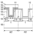
도 1은 본 발명의 제1 실시예에 따른 반도체 장치의 단면도이다.1 is a cross-sectional view of a semiconductor device according to a first embodiment of the present invention.
도 1을 참조하면, 반도체 기판(100)은 제1 영역(예를 들어, NFET 영역)과 제2 영역(예를 들어, PFET 영역)을 포함할 수 있다. 여기서, 제1 영역(NFET)은 N타입 전계 효과 트랜지스터(NFET)가 형성되는 영역일 수 있고, 제2 영역(PFET)은 P타입 전계 효과 트랜지스터(PFET)가 형성되는 영역일 수 있다.Referring to FIG. 1, the
제1 및 제2 영역(NFET, PFET)은 각각 채널 영역(C)과 소오스 및 드레인 영역(101, 102)을 포함할 수 있다. 여기서, 제1 영역(NFET)의 채널 영역(C)은 소오스 및 드레인 영역(101)에 포함된 N타입 캐리어(carrier)가 이동되는 영역일 수 있고, 제2 영역(PFET)의 채널 영역(C)은 소오스 및 드레인 영역(102)에 포함된 P타입 캐리어(carrier)가 이동되는 영역일 수 있다. 한편, 비록 도시하지는 않았으나 소오스 및 드레인 영역(101, 102)의 외측으로는 반도체 기판(100)에 형성된 소자들을 분리하는 소자 분리막(미도시)이 형성될 수 있다.The first and second regions NFET and PFET may include a channel region C and source and drain
제1 영역(NFET)의 채널 영역(C) 상에는 제1 트렌치(111)가 형성될 수 있다. 구체적으로, 제1 영역(NFET)의 채널 영역(C) 상에는 스페이서(120)로 둘러쌓인 제1 트렌치(111)가 형성될 수 있으며, 스페이서(120)의 외측에는 층간 절연막(110)이 형성될 수 있다. 본 발명의 몇몇 실시예에서, 층간 절연막(110)에는, NFET에 인장 응력(tensile stress)을 제공하기 위한 스트레스막(미도시)이 추가적으로 형성될 수 있다. 한편, 스페이서(120)의 형상은 도시된 형상에 제한되지 않고, 필요에 따라 L자형 등으로 변형될 수 있다.The
제1 트렌치(111) 내부에는 인터페이스막(125), 제1 고유전율(high-K)막(131), 확산막(140), 보호막(150), 및 제1 메탈 게이트 구조물(161)이 순차적으로 형성될 수 있다. 이 때, 제1 고유전율막(131), 확산막(140), 보호막(150), 및 제1 메탈 게이트 구조물(161)은 모두 도시된 것과 같이 제1 트렌치(111)의 측벽을 따라 상부로 연장되어 형성될 수 있다.Inside the
인터페이스막(125)은, 반도체 기판(100)과 제1 고유전율막(131) 사이의 불량 계면을 방지하는 역할을 할 수 있다. 인터페이스막(125)은 유전율(k)이 9 이하인 저유전 물질층, 예를 들면 실리콘 산화막(k는 약 4) 또는 실리콘 산질화막 (산소 원자 및 질소 원자 함량에 따라 k는 약 4~8)을 포함할 수 있다. 또는, 인터페이스막(125)은 실리케이트로 이루어질 수도 있으며, 앞서 예시된 막들의 조합으로 이루어질 수도 있다.The
인터페이스막(125) 상에 형성된 제1 고유전율막(131)은, 고유전율을 갖는 물질로 이루어질 수 있다. 본 발명의 몇몇 실시예에서, 이러한 제1 고유전율막(131)은 예를 들어, HfO2, Al2O3, ZrO2, TaO2 등의 물질로 이루어질 수 있으나, 본 발명이 이에 제한되는 것은 아니다.The first high dielectric
제1 고유전율막(131) 상에는 확산막(140)이 형성될 수 있다. 본 실시예에서, 확산막(140)은 예를 들어, 메탈 산화막일 수 있다. 구체적으로, 확산막(140)은 LaO, Y2O3, Lu2O3, SrO 또는 이들의 조합일 수 있으나, 본 발명이 이에 제한되는 것은 아니다. 확산막(140)에 포함된 물질(예를 들어, 메탈)이 NFET의 채널 영역(C)으로 확산됨으로써 NFET의 워크펑션(work function)이 조절되게 되는데, 이에 따라 NFET의 성능을 향상시킬 수 있다. The
또한, 확산막(140)에 포함된 물질(예를 들어, 메탈)은 그 하부에 형성된 제1 고유전율막(131)에도 확산될 수 있는데, 이에 따라 제1 고유전율막(130)의 유전율이 높아져 NFET의 게이트 누설 전류가 저감될 수 있다. 한편, 확산막(140)은 후술할 제1 메탈 게이트 구조물(161)에 포함된 메탈이 제1 고유전율막(131)으로 침투되는 것을 방지하는 역할도 함으로써 NFET의 성능 향상에 도움을 줄 수 있다. 본 실시예에 따른 확산막(140)의 이러한 기능에 대해서는, 추후 본 실시예에 따른 반도체 장치의 제조 방법을 설명하면서 보다 구체적으로 설명하도록 한다.In addition, a material (eg, a metal) included in the
본 발명의 몇몇 실시예에서, 확산막(140)은 제1 고유전율막(131) 상에 제1 두께로 형성될 수 있다. 여기서, 제1 두께는 예를 들어, 3 내지 10Å일 수 있으나, 본 발명이 이에 제한되는 것은 아니다.In some embodiments of the present invention, the
확산막(140) 상에는 보호막(150)이 형성될 수 있다. 이러한 보호막(150)은 후술할 제조 공정 상에서 확산막(140)이 산화되는 것을 방지하는 역할을 할 수 있다. 본 실시예에서, 보호막(150)은 예를 들어, 메탈 질화막일 수 있다. 구체적으로, 보호막(150)은 예를 들어, TiN, TaN 중 적어도 하나를 포함도록 구성될 수 있다. 더욱 구체적으로, 보호막(150)은 예를 들어, TiN으로 이루어진 단일막, 또는 TiN 하부막과 TaN 상부막으로 이루어진 이중막 등으로 이루어질 수 있으나, 본 발명이 이에 제한되는 것은 아니다.The
본 발명의 몇몇 실시예에서, 보호막(140)은 제1 두께의 확산막(140) 보다 두꺼운 제2 두께로 형성될 수 있다. 구체적으로, 보호막(140)은 예를 들어, 11 내지 70Å의 두께로 형성될 수 있으나, 본 발명이 이에 제한되는 것은 아니다.In some embodiments of the present disclosure, the
보호막(150)의 상에는 제1 메탈 게이트 구조물(161)이 형성될 수 있다. 이러한 제1 메탈 게이트 구조물(161)은 메탈로 이루어진 단일막, 또는 메탈 질화막과 메탈로 이루어진 다층막 구조일 수 있다. 제1 메탈 게이트 구조물(161)을 이루는 메탈로는 예를 들어, Al, W, Ti 또는 이들의 조합 등을 들 수 있고, 메탈 질화막으로는 TiN, TaN 또는 이들의 조합 등을 들 수 있으나, 본 발명이 이에 제한되는 것은 아니다. 본 실시예에서, 이러한 제1 메탈 게이트 구조물(161)은 대체 메탈 게이트(RMG, replacement metal gate) 공정을 이용하여 형성될 수 있다. 이에 대해서는 추후 본 실시예에 따른 반도체 장치의 제조 방법을 설명하면서 보다 구체적으로 설명하도록 한다.The first
본 발명의 몇몇 실시예에서, 제1 메탈 게이트 구조물(161)은 N타입 워크펑션막(미도시)을 포함할 수 있다. 이러한, N타입 워크펑션막(미도시)의 예로는, TiAl, TiAlN, TaC, TaAlN, TiC, HfSi 등을 들 수 있으나, 본 발명이 이에 제한되는 것은 아니다. 이러한, N타입 워크펑션막(미도시)은, 예를 들어, 30 내지 120Å 두께로 형성될 수 있으나, 역시 본 발명이 이에 제한되는 것은 아니다.In some embodiments of the present invention, the first
제2 영역(PFET)의 채널 영역(C) 상에는 제2 트렌치(112)가 형성될 수 있다. 구체적으로, 제2 영역(PFET)의 채널 영역(C) 상에는 스페이서(120)로 둘러쌓인 제2 트렌치(112)가 형성될 수 있으며, 스페이서(120)의 외측에는 층간 절연막(110)이 형성될 수 있다. 본 발명의 몇몇 실시예에서 제2 영역(PFET)에 형성된 층간 절연막(110)에는, PFET에 압축 응력(compressive stress)을 제공하기 위한 스트레스막(미도시)이 추가적으로 더 형성될 수 있다. 또한, 마찬가지로 스페이서(120)의 형상은 도시된 형상에 제한되지 않으며, 필요에 따라 L자형 등으로 변형될 수 있다.The
제2 트렌치(112) 내부에는 인터페이스막(125), 제2 고유전율막(132) 및 제2 메탈 게이트 구조물(162)이 순차적으로 형성될 수 있다. 앞서와 마찬가지로, 제2 고유전율막(132) 및 제2 메탈 게이트 구조물(162)은 모두 도시된 것과 같이 제2 트렌치(112)의 측벽을 따라 상부로 연장되어 형성될 수 있다.The
제2 고유전율막(132)은 앞서 설명한 제1 고유전율막(131)과 동일하게 고유전율을 갖는 물질로 이루어질 수 있다. 본 발명의 몇몇 실시예에서, 제2 고유전율막(132)은 앞서 설명한 제1 고유전율막(131)과 실질적으로 동일한 물질로 이루어질 수 있다.The second high dielectric
제2 고유전율막(132) 상에는 제2 메탈 게이트 구조물(162)이 형성될 수 있다. 제2 메탈 게이트 구조물(162)은 메탈로 이루어진 단일막, 또는 메탈 질화막과 메탈로 이루어진 다층막 구조일 수 있다.The second
본 발명의 몇몇 실시예에서, 제2 메탈 게이트 구조물(162)을 구성하는 메탈 또는 메탈 질화막은, 제1 메탈 게이트 구조물(161)을 구성하는 메탈 또는 메탈 질화막과 서로 다를 수 있다. 구체적으로, 예를 들어, 제1 메탈 게이트 구조물(161)은 TiAl/TiN/Ti/Al의 4중막으로 이루어질 수 있고, 제2 메탈 게이트 구조물(162)은 TiN/TaN/TiN/Al의 4중막으로 이루어질 수 있으나, 본 발명이 이에 제한되는 것은 아니다.In some embodiments of the present disclosure, the metal or metal nitride film constituting the second
본 발명의 몇몇 실시예에서, 제2 메탈 게이트 구조물(162)은 P타입 워크펑션막(미도시)을 포함할 수 있다. 이러한 P타입 워크펑션막(미도시)은 예를 들어, 50 내지 100Å 두께로 형성될 수 있으나, 본 발명이 이에 제한되는 것은 아니다. 또한, 본 발명의 다른 몇몇 실시예에서, 제2 메탈 게이트 구조물(162)은 하부 P타입 워크펑션막(미도시)과 상부 N타입 워크펑션막(미도시)을 모두 포함할 수도 있다.In some embodiments of the present disclosure, the second
비록 도면에 도시하지는 않았으나, 소오스 및 드레인 영역(101, 102) 상에는, NFET 및 PFET과 층간 절연막(110) 상부에 형성된 컨택(미도시)을 전기적으로 연결하기 위한 연결 배선(미도시)이 층간 절연막(110)을 관통하여 형성될 수 있다.Although not shown in the drawings, on the source and drain
이처럼, 본 실시예에 따른 반도체 장치에서는, NFET에 확산막(140)이 형성되어 NFET의 성능을 향상시키고, PFET에도 P타입 워크펑션막(미도시)이 형성되어 PFET의 성능 향상시키므로, 반도체 장치 전체의 성능이 크게 개선될 수 있다.As described above, in the semiconductor device according to the present embodiment, the
이러한 본 실시예에 따른 반도체 장치는 다양한 방법을 통해 제조하는 것이 가능하다. 이하에서는, 앞서 설명한 본 실시예에 따른 반도체 장치의 예시적인 제조 방법에 대해 설명하도록 한다.The semiconductor device according to the present embodiment can be manufactured by various methods. Hereinafter, an exemplary manufacturing method of the semiconductor device according to the present embodiment described above will be described.
도 2 내지 도 6은 본 발명의 제1 실시예에 따른 반도체 장치의 제조 방법을 설명하기 위한 중간 단계 도면들이다.2 to 6 are intermediate steps for explaining a method of manufacturing a semiconductor device according to the first embodiment of the present invention.
먼저, 도 2를 참조하면, 반도체 기판(100) 상에 게이트 절연막(102)과 제1 폴리 게이트(104)를 포함하는 더미 게이트(105)를 형성한다. 이어서, 더미 게이트(105)를 마스크로 반도체 기판(100)에 불순물을 주입하여 소오스 및 드레인 영역(101, 102)을 형성한다. 이어서, 더미 게이트(105)의 양측에 스페이서(120)를 형성한다. 이 때, 스페이서(120)의 형상은 앞서 설명한 것과 같이 도시된 형상에 제한되지 않는다. 그 후, 더미 게이트(105)를 덮도록 반도체 기판(100) 상에 층간 절연막(110)을 형성한다. 그리고, 더미 게이트(105)의 상면이 노출되도록 층간 절연막(110)을 평탄화한다.First, referring to FIG. 2, a
다음 도 3을 참조하면, 상면이 노출된 더미 게이트(도 2의 105)를 제거한다. 이 때, 더미 게이트(105)를 제거하는 방법으로는, 대체 메탈 게이트(RMG, replacement metal gate) 공정에서 사용하는 다양한 방법이 사용될 수 있으며, 여기서는 불필요한 오해를 줄이기 위해 자세한 그 제거 방법에 대해서는 설명을 생략하도록 한다. 이렇게 반도체 기판(100)의 제1 영역(NFET)에 형성된 더미 게이트(도 2의 105)가 제거되면 제1 트렌치(111)가 형성되고, 반도체 기판(100)의 제2 영역(PFET)에 형성된 더미 게이트(105)가 제거되면 제2 트렌치(112)가 형성된다.Next, referring to FIG. 3, the dummy gate (105 of FIG. 2) having the top surface exposed is removed. In this case, as a method of removing the
다음, 도 4를 참조하면, 제1 및 제2 트렌치(111, 112) 내에 인터페이스막(125)을 형성한다. 여기서, 인터페이스막(125)은 반도체 기판(100)과 후술할 고유전율막(130) 사이의 불량 계면을 방지하는 역할을 할 수 있다. 인터페이스막(125)은 유전율(k)이 9 이하인 저유전 물질층, 예를 들면 실리콘 산화막(k는 약 4) 또는 실리콘 산질화막 (산소 원자 및 질소 원자 함량에 따라 k는 약 4~8)을 포함할 수 있다. 또는, 인터페이스막(125)은 실리케이트로 이루어질 수도 있으며, 상기 예시된 막들의 조합으로 이루어질 수도 있다.Next, referring to FIG. 4, the
이어서, 제1 트렌치(111)와 제2 트렌치(112) 내에, 고유전율막(130), 확산막(140), 및 보호막(150)을 순차적으로 형성한다. 본 실시예에서, 확산막(140)은 예를 들어, 메탈 산화막일 수 있으며, 보호막(150)은 예를 들어, 메탈 질화막일 수 있다. 구체적으로, 확산막(140)은 예를 들어, LaO, Y2O3, Lu2O3, SrO 또는 이들의 조합일 수 있으며, 보호막(150)은 예를 들어, TiN, TaN 또는 이들의 조합일 수 있다. 더욱 구체적으로, 확산막(140)은 LaO일 수 있으며, 보호막(150)은 TiN일 수 있다.Subsequently, the high dielectric
확산막(140)은 CVD 또는 ALD 등을 통해 예를 들어, 3 내지 10Å의 두께로 형성될 수 있으며, 보호막(150) 역시 CVD 또는 ALD 등을 통해 예를 들어, 11 내지 70Å의 두께로 형성될 수 있다.The
다음 도 5를 참조하면, 반도체 기판(100)의 제1 영역(NFET) 상에 선택적으로 폴리 실리콘막(135)을 형성한다. 그리고 이어서, 노출된 보호막(150) 및 확산막(140)을 순차적으로 제거한다. 이에 따라, 도시된 것과 같이 제2 트렌치(112) 내에 형성된 보호막(150)과 확산막(140)이 제거될 수 있다.Next, referring to FIG. 5, a
이어서, 반도체 기판(100)을 열처리한다. 반도체 기판(100)이 열처리되는 동안 제1 트렌치(111) 내에 형성된 확산막(140)에 포함된 물질(예를 들어, 메탈)은 제1 트렌치(11) 내에 형성된 고유전율막(130)과 NFET의 채널 영역(C)으로 확산될 수 있다. 한편, 제2 트렌치(112) 내에는 이러한 확산막(140)이 형성되어 있지 않으므로 제2 트렌치(112) 내에 형성된 고유전율막(130)과 PFET의 채널 영역(C)은 열처리 과정에서 확산막(140)의 영향을 받지 않게된다.Next, the
앞서 설명한 것과 같이, 제1 트렌치(111) 내에 형성된 고유전율막(130)으로 확산된 확산막(140)의 메탈 성분(예를 들어, La)은 제1 트렌치(111) 내에 형성된 고유전율막(130)의 유전율을 증가시킬 수 있다. 또한, NFET의 채널 영역(C)으로 확산된 확산막(140)의 메탈 성분(예를 들어, La)은 NFET의 워크펑션을 조절하여 NFET의 성능을 향상시킬 수 있다.As described above, the metal component (eg, La) of the
이 때, 보호막(150)은 열처리 과정에서 확산막(140)이 산화되는 것을 방지하는 역할을 할 수 있다. 본 실시예에서, 이러한 열처리가 수행되는 동안 반도체 기판(100)의 제1 영역(NFET) 상에는 폴리 실리콘막(135)이 형성되어 있으므로, 보호막(150)은 열처리 과정에서 확산막(140)이 폴리 실리콘막(135)으로부터 산화되는 것을 방지하는 역할을 할 수 있다.In this case, the
다음 도 1을 참조하면, 애싱(ashing) 등의 공정을 통해 반도체 기판(100)의 제1 영역(NFET) 상에 형성된 폴리 실리콘막(도 5의 135)을 제거한다. 이어서, 제1 트렌치(111) 내에 형성된 보호막(150) 상에 예를 들어, TiAl, TiN, Ti, 및 Al을 순차적으로 형성한 후, Al CMP 공정을 수행하여 도시된 제1 메탈 게이트 구조물(161)을 형성할 수 있다. 하지만, 본 실시예에 따른 제1 메탈 게이트 구조물(161)의 구성이 이러한 예시에 제한되는 것은 아니며, 필요에 따라 그 구성은 앞서 설명한 것과 같이 얼마든지 변형될 수 있다. 한편, 제1 메탈 게이트 구조물(161)은 앞서 설명한 것과 같이 NFET의 성능 향상을 위한 N타입 워크펑션막(미도시)을 포함할 수 있다. Next, referring to FIG. 1, a polysilicon film (135 of FIG. 5) formed on the first region NFET of the
이어서, 제2 트렌치(112) 내에 형성된 고유전율막(도 5의 130) 상에 예를 들어, TaN, TiN, 및 Al을 순차적으로 형성한 후, Al CMP 공정을 수행함으로써, 제2 메탈 게이트 구조물(162)을 형성한다. 이 때, 제2 메탈 게이트 구조물(162)은 앞서 설명한 것과 같이 PFET의 성능 향상을 위한 P타입 워크펑션막(미도시) 또는, 하부 P타입 워크펑션막(미도시)과 상부 N타입 워크펑션막(미도시)을 포함할 수 있다. Subsequently, for example, TaN, TiN, and Al are sequentially formed on the high dielectric constant film 130 (see FIG. 5) formed in the
이렇게 제1 및 제2 게이트 메탈 구조물(161, 162)의 형성이 완료되면, 비록 도시하지는 않았으나, NFET 및 PFET과 층간 절연막(110) 상부에 형성된 컨택(미도시)을 전기적으로 연결하기 위한 연결 배선(미도시)을 층간 절연막(110)을 관통하도록 형성할 수 있다.When the formation of the first and second
이상에서는 본 발명의 제1 실시예에 따른 반도체 장치의 제조 방법에 대한 일 예를 설명하였으나, 본 발명이 이에 제한되는 것은 아니다. 이하에서는, 본 발명의 제1 실시예에 따른 반도체 장치의 제조 방법에 대한 다른 예를 설명하도록 한다.In the above, an example of a method of manufacturing the semiconductor device according to the first embodiment of the present invention has been described, but the present invention is not limited thereto. Hereinafter, another example of the method of manufacturing the semiconductor device according to the first embodiment of the present invention will be described.
먼저, 도 2 내지 도 4에 도시된 것과 같이, 제1 영역(NFET)과 제2 영역(PFET)을 포함하는 반도체 기판(100)과, 제1 및 제2 영역(NFET, PFET)에 각각 형성된 제1 및 제2 트렌치(111, 112)를 준비한다. 그리고, 제1 및 제2 트렌치(111, 112) 내에 각각 인터페이스막(125), 고유전율막(130), 확산막(140), 및 보호막(150)을 순차적으로 형성한다. 이에 대해서는 앞서 충분히 설명한바, 중복된 설명은 생략하도록 한다.First, as shown in FIGS. 2 to 4, the
이어서, 도 6을 참조하면, 반도체 기판(100)의 제1 영역(NFET) 상에 선택적으로 폴리 실리콘막(미도시)을 형성한 후, 노출된 제2 트렌치(112) 내에 형성된 보호막(150) 및 확산막(140)을 순차적으로 제거한다. 이어서, 애싱(ashing) 등의 공정을 통해 반도체 기판(100)의 제1 영역(NFET) 상에 형성된 폴리 실리콘막(미도시)을 제거한다.Subsequently, referring to FIG. 6, after the polysilicon film (not shown) is selectively formed on the first region NFET of the
이어서, 반도체 기판(100)을 열처리한다. 반도체 기판(100)이 열처리되는 동안 제1 트렌치(111) 내에 형성된 확산막(140)에 포함된 물질(예를 들어, 메탈)은 제1 트렌치(11) 내에 형성된 고유전율막(130)과 NFET의 채널 영역(C)으로 확산될 수 있다. Next, the
이 때, 반도체 기판(100)의 제1 영역(NFET) 상에는 폴리 실리콘막(135)이 형성되어 있지 않으므로, 확산막(150)은 외부로 노출된 상태일 수 있다. 따라서, 이 경우, 보호막(150)은 열처리 과정에서 확산막(140)이 외부 환경으로부터 산화되는 것을 방지하는 역할을 할 수 있다.In this case, since the
이후, 제1 트렌치(111) 내에 제1 메탈 게이트 구조물(161)을 형성하고, 제2 트렌치(112) 내에 제2 메탈 게이트 구조물(162)을 형성하는 것은, 앞서 설명한 것과 동일한 바, 중복된 설명은 생략하도록 한다.Subsequently, forming the first
이상에서 본 발명의 제1 실시예에 따른 반도체 장치 및 그 예시적인 제조 방법들에 대해 설명하였으나, 본 발명이 이에 제한되는 것은 아니며, 그 구조 및 제조 방법들은 본 발명의 기술적 사상의 범위 내에서 얼마든지 변형될 수 있다.Although the semiconductor device and the exemplary manufacturing methods thereof according to the first embodiment of the present invention have been described above, the present invention is not limited thereto, and the structure and the manufacturing method thereof are not limited within the scope of the technical idea of the present invention. Can be transformed.
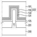
다음 도 7을 참조하여, 본 발명의 제2 실시예에 따른 반도체 장치에 대해 설명하도록 한다.Next, a semiconductor device according to a second exemplary embodiment of the present invention will be described with reference to FIG. 7.
도 7은 본 발명의 제2 실시예에 따른 반도체 장치의 단면도이다. 이하에서는 앞서 설명한 실시예들과 중복된 설명은 생략하도록 하고, 그 차이점을 위주로 설명하도록 한다.7 is a sectional view of a semiconductor device according to a second embodiment of the present invention. Hereinafter, the description overlapping with the embodiments described above will be omitted, and the differences will be mainly described.
도 7을 참조하면, 본 실시예에 따른 반도체 장치의 제2 트렌치(112) 내에는 제1 트렌치(111)와 동일하게 확산막(140)과 보호막(150)이 순차적으로 형성될 수 있다. 하지만, 본 실시예에서 제2 트렌치(112) 내에 형성된 확산막(140)의 하부에는, 확산막(140)의 확산을 방지하는 확산 방지막(170)이 추가로 형성될 수 있다.Referring to FIG. 7, the
확산 방지막(170)은 도시된 것과 같이 제2 트렌치(112)의 측벽을 따라 상부로 연장되어 형성될 수 있다. 이러한 확산 방지막(170)은 예를 들어, 메탈 산화막으로 이루어진 확산막(140)의 메탈이 제2 고유전율막(132)이나 PFET의 채널 영역(C)으로 확산되는 것을 방지하는 역할을 할 수 있다. 따라서, 본 실시예에 따른 반도체 장치는 앞서 설명한 실시예들과 달리, 제2 트렌치(112) 내에도 확산막(140)과 보호막(150)이 순차적으로 형성되어있으나, 확산 방지막(170)의 존재로 인해, 앞서 설명한 실시예들과 동일한 효과를 가질 수 있다.The
본 발명의 몇몇 실시예에서, 확산 방지막(170)은 P타입 워크펑션막을 포함할 수 있다. 이러한 확산 방지막(170)의 예로는, 메탈 질화막을 들 수 있다. 구체적으로, 확산 방지막(170)은 예를 들어, TiN막일 수 있으나, 본 발명이 이에 제한되는 것은 아니다. 또한, 본 발명의 다른 몇몇 실시예에서, 확산 방지막(170)은 메탈 질화막과 메탈을 포함하는 이중막 구조일 수 있다. 구체적으로, 확산 방지막(170)은 예를 들어, TiN과 Al을 포함하는 이중막 구조일 수 있으나, 본 발명이 이에 제한되는 것은 아니다. 본 발명의 또 다른 몇몇 실시예에서, 확산 방지막(170)은 예를 들어, 제1 메탈 질화막, 메탈, 및 제2 메탈 질화막을 포함하는 삼중막 구조일 수 있다. 구체적으로, 확산 방지막(170)은 예를 들어, TiN, Al, TiN으로 이루어진 삼중막 구조일 수 있으나, 본 발명이 이에 제한되는 것은 아니다. 이러한 확산 방지막(170)의 두께는 예를 들어, 1 내지 100Å일 수 있으나, 본 발명이 이에 제한되는 것은 아니다.In some embodiments of the present disclosure, the
이하, 도 3 및 도 7 내지 도 10을 참조하여, 이러한 본 발명의 제2 실시예에 따른 반도체 장치의 예시적인 제조 방법에 대해 설명하도록 한다.Hereinafter, an exemplary manufacturing method of the semiconductor device according to the second exemplary embodiment of the present invention will be described with reference to FIGS. 3 and 7 to 10.
도 8 내지 도 10은 본 발명의 제2 실시예에 따른 반도체 장치의 제조 방법을 설명하기 위한 중간 단계 도면들이다.8 to 10 are intermediate step views for describing a method of manufacturing a semiconductor device according to a second embodiment of the present invention.
먼저, 도 3에 도시된 것과 같이, 반도체 기판(100)의 제1 영역(NFET)에 제1 트렌치(111)를 형성하고, 반도체 기판(100)의 제2 영역(PFET)에 제2 트렌치(112)를 형성한다. 이에 대해서는 앞서 충분히 설명한바, 중복된 설명은 생략하도록 한다.First, as shown in FIG. 3, the
다음 도 8을 참조하면, 제1 및 제2 트렌치(111, 112) 내에 인터페이스막(125)을 형성한다. 그리고, 제1 트렌치(111)와 제2 트렌치(112) 내에, CVD 또는 ALD 등을 통해 고유전율막(130) 및 확산 방지막(170)을 순차적으로 형성한다.Next, referring to FIG. 8, the
본 발명의 몇몇 실시예에서, 확산 방지막(170)은 P타입 워크펑션막을 포함할 수 있다. 이러한 확산 방지막(170)의 예로는, 메탈 질화막을 들 수 있다. 구체적으로, 확산 방지막(170)은 예를 들어, TiN막일 수 있으나, 본 발명이 이에 제한되는 것은 아니다. 또한, 본 발명의 다른 몇몇 실시예에서, 확산 방지막(170)은 메탈 질화막과 메탈을 포함하는 이중막 구조일 수 있다. 구체적으로, 확산 방지막(170)은 예를 들어, TiN과 Al을 포함하는 이중막 구조일 수 있으나, 본 발명이 이에 제한되는 것은 아니다. 본 발명의 또 다른 몇몇 실시예에서, 확산 방지막(170)은 예를 들어, 제1 메탈 질화막, 메탈, 및 제2 메탈 질화막을 포함하는 삼중막 구조일 수 있다. 구체적으로, 확산 방지막(170)은 예를 들어, TiN, Al, TiN으로 이루어진 삼중막 구조일 수 있으나, 본 발명이 이에 제한되는 것은 아니다. 확산 방지막(170)은 예를 들어, 1 내지 100Å의 두께로 형성할 수 있으나, 본 발명이 이에 제한되는 것은 아니다.In some embodiments of the present disclosure, the
이어서, 반도체 기판(100)의 제2 영역(PFET)을 마스킹하고, 반도체 기판(100)의 제1 영역(NFET)에 형성된 확산 방지막(170)을 선택적으로 제거한다. 그 결과, 확산 방지막(170)은 제2 트렌치(112) 내에는 존재하나, 제1 트렌치(111) 내에는 존재하지 않을 수 있다.Subsequently, the second region PFET of the
다음 도 9를 참조하면, 제1 트렌치(111)와 제2 트렌치(112) 각각에 확산막(140)과 보호막(150)을 CVD 또는 ALD 등을 통해 순차적으로 형성한다. 이 때, 확산막(140)은 예를 들어, 3 내지 10Å의 두께로 형성될 수 있으며, 보호막(150)은 예를 들어, 11 내지 70Å의 두께로 형성될 수 있다. 이에 따라, 제1 트렌치(111) 내에 형성된 확산막(140)의 하부에는 확산 방지막(170)이 형성되지 않고, 제2 트렌치(112) 내에 형성된 확산막(140)의 하부에는 확산 방지막(170)이 형성될 수 있다.Next, referring to FIG. 9, the
다음 도 10을 참조하면, 제1 트렌치(111)와 제2 트렌치(112) 각각에 확산막(140)과 보호막(150)이 형성된 반도체 기판(100)을 열처리 한다. 이 때, 제2 트렌치(112) 내에 형성된 확산막(140) 하부에는 확산 방지막(170)이 형성되어 있기 때문에, 확산막(140)에 포함된 물질(예를 들어, 메탈)이 제2 트렌치(112) 내에 형성된 고유전율막(130)이나 PFET의 채널 영역(C)으로 확산되지 못한다. 따라서, 확산막(140)에 포함된 물질(예를 들어, 메탈)은 도시된 것과 같이 제1 트렌치(111) 내에 형성된 고유전율막(130)과 NFET의 채널 영역(C)에만 선택적으로 확산되게 된다.Next, referring to FIG. 10, the
다음 도 7을 참조하면, 제1 트렌치(111) 내에 형성된 보호막(150) 상에 제1 메탈 게이트 구조물(161)을 형성한다. 또한, 제2 트렌치(112) 내에 형성된 보호막(150) 상에 제2 메탈 게이트 구조물(162)을 형성한다. 이에 대해서는 앞서 충분히 설명한바, 중복된 설명은 생략하도록 한다.Next, referring to FIG. 7, the first
다음 도 11을 참조하여, 본 발명의 제3 실시예에 따른 반도체 장치에 대해 설명하도록 한다.Next, a semiconductor device according to a third exemplary embodiment of the present invention will be described with reference to FIG. 11.
도 11은 본 발명의 제3 실시예에 따른 반도체 장치의 단면도이다. 이하에서도 앞서 설명한 실시예들과 중복된 설명은 생략하도록 하고, 그 차이점을 위주로 설명하도록 한다.11 is a sectional view of a semiconductor device according to a third embodiment of the present invention. Hereinafter, a description overlapping with the above-described embodiments will be omitted, and the difference will be mainly described.
도 11을 참조하면, 본 실시예에 따른 반도체 장치의 제2 트렌치(112) 내에 형성된 제2 메탈 게이트 구조물(162) 하부에는 코발트막(cobalt layer)(175)이 더 형성될 수 있다. 이러한 코발트막(175)은 그 상부에 형성되는 메탈의 메탈-필(metal-fill) 특성을 향상시킬 수 있다. 즉, 도시된 것과 같이 제2 트렌치(112) 내에 형성된 보호막(150) 상에 코발트막(175)이 형성될 경우, 그 상부에 제2 메탈 게이트 구조물(162)이 형성될 시, 메탈-필 특성이 향상되므로, 제2 메탈 게이트 구조물(162)이 제2 트렌치(112) 내에 보다 신뢰성 있게 형성될 수 있다.Referring to FIG. 11, a
이러한 코발트막(175)은 CVD 공정 등을 통해 보호막(150) 상에 형성할 수 있다. 이 때, 코발트막(175)의 두께는 예를 들어, 1 내지 20Å일 수 있으나, 본 발명이 이에 제한되는 것은 아니다.The
다음 도 12를 참조하여, 본 발명의 제4 실시예에 따른 반도체 장치에 대해 설명하도록 한다.Next, a semiconductor device according to a fourth embodiment of the present invention will be described with reference to FIG. 12.
도 12는 본 발명의 제4 실시예에 따른 반도체 장치의 단면도이다. 이하에서도 앞서 설명한 실시예들과 중복된 설명은 생략하도록 하고, 그 차이점을 위주로 설명하도록 한다.12 is a sectional view of a semiconductor device according to a fourth embodiment of the present invention. Hereinafter, a description overlapping with the above-described embodiments will be omitted, and the difference will be mainly described.
도 12를 참조하면, 본 실시예에 따른 반도체 장치의 제2 트렌치(112) 내에 형성된 확산 방지막(170)은 도시된 것 같이 그 양단이 챔퍼링된(chamfered) 형상일 수 있다. 구체적으로, 확산 방지막(170)은 제2 트렌치(112)의 측벽을 따라 상부로 연장된 U자형으로 형성되되, 그 상면이 제2 트렌치(112)의 상면보다 낮게 형성될 수 있다.Referring to FIG. 12, the
확산 방지막(170)의 형상을 이와 같이 형성할 경우, 그 상부에 형성되는 메탈의 메탈-필 특성이 향상될 수 있다. 따라서, 확산 방지막(170) 상부에 제2 메탈 게이트 구조물(162)이 도시된 것과 같이 형성될 시, 메탈-필 특성이 향상되므로, 제2 메탈 게이트 구조물(162)이 제2 트렌치(112) 내에 보다 신뢰성 있게 형성될 수 있다.When the
다음 도 13 내지 도 15를 참조하여, 본 발명의 제5 실시예에 따른 반도체 장치에 대해 설명한다.Next, a semiconductor device according to a fifth embodiment of the present invention will be described with reference to FIGS. 13 to 15.
도 13은 본 발명의 제5 실시예에 따른 반도체 장치를 설명하기 위한 도면이다. 도 14는 도 13의 A-A′를 따라 절단한 단면도이다. 도 15는 도 13의 B-B′를 따라 절단한 단면도이다. 도 13 내지 도 15에는, 도 1에 도시된 NFET의 게이트가 핀형 트랜지스터(Fin FET)에 적용된 것을 도시하였다.13 is a diagram for describing a semiconductor device according to example embodiments of the present inventive concepts. 14 is a cross-sectional view taken along line AA ′ of FIG. 13. FIG. 15 is a cross-sectional view taken along line BB ′ of FIG. 13. 13 to 15 show that the gate of the NFET shown in FIG. 1 is applied to a fin FET.
도 13 내지 도 15를 참조하면, 본 발명의 제5 실시예에 따른 반도체 장치는 핀(F1), 게이트 전극(222), 리세스(225), 소오스 및 드레인(261) 등을 포함할 수 있다. 13 to 15, the semiconductor device according to the fifth embodiment of the present invention may include a fin F1, a
핀(F1)은 제2 방향(Y1)을 따라서 길게 연장될 수 있다. 핀(F1)은 기판(200)의 일부일 수도 있고, 기판(200)으로부터 성장된 에피층(epitaxial layer)을 포함할 수 있다. 소자 분리막(201)은 핀(F1)의 측면을 덮을 수 있다.The fin F1 may extend long along the second direction Y1. The fin F1 may be part of the
게이트 전극(222)은 핀(F1) 상에, 핀(F1)과 교차하도록 형성될 수 있다. 게이트 전극(222)은 제1 방향(X1)으로 연장될 수 있다. The
도시된 것과 같이, 인터페이스막(125)과 제1 고유전율막(131) 상에 형성된 게이트 전극(222)은, 확산막(140), 보호막(150), 및 제1 메탈 게이트 구조물(161) 등을 포함할 수 있다.As illustrated, the
리세스(225)는 게이트 전극(222) 양측의 제2 층간 절연막(202) 내에 형성될 수 있다. 리세스(225)의 측벽은 경사져 있어서, 리세스(225)의 형상은 기판(100)에서 멀어질수록 넓어질 수 있다. 한편, 도 13에 도시된 것처럼, 리세스(225)의 폭은 핀(F1)의 폭보다 넓을 수 있다. The
소오스 및 드레인(261)은 리세스(225) 내에 형성될 수 있다. 소오스 및 드레인(261)은 상승된(elevated) 소오스 및 드레인 형태일 수 있다. 즉, 소오스 및 드레인(261)의 상면은 제1 층간 절연막(201)의 상면보다 높을 수 있다. 또한, 소오스 및 드레인(261)과 게이트 전극(222)은 스페이서(120)에 의하여 절연될 수 있다.Source and drain 261 may be formed in
본 발명의 반도체 장치가, NFET인 경우, 소오스 및 드레인(261)은 기판(200)과 동일 물질 또는, 인장 스트레스 물질을 포함할 수 있다. 예를 들어, 기판(200)이 Si을 포함할 때, 소오스 및 드레인(261)은 Si을 포함하거나, Si 보다 격자 상수가 작은 물질(예를 들어, SiC)을 포함할 수 있다. 이러한 인장 스트레스 물질은 핀(F1)에 인장 스트레스를 가하여 채널 영역의 캐리어의 이동도(mobility)를 향상시킬 수 있다. When the semiconductor device of the present invention is an NFET, the source and drain 261 may include the same material as the
다음 도 16 내지 도 18를 참조하여, 본 발명의 제6 실시예에 따른 반도체 장치에 대해 설명한다.Next, a semiconductor device according to a sixth embodiment of the present invention will be described with reference to FIGS. 16 to 18.
도 16은 본 발명의 제6 실시예에 따른 반도체 장치를 설명하기 위한 도면이다. 도 17은 도 16의 C-C′를 따라 절단한 단면도이다. 도 18은 도 16의 D-D′를 따라 절단한 단면도이다. 도 16 내지 도 18에는, 도 12에 도시된 PFET의 게이트가 핀형 트랜지스터(Fin FET)에 적용된 것을 도시하였다. 이하에서는, 앞서 설명한 실시예와 차이점에 대해서만 설명하도록 한다.16 is a diagram for describing a semiconductor device according to example embodiments of the present inventive concepts. FIG. 17 is a cross-sectional view taken along line CC ′ of FIG. 16. FIG. 18 is a cross-sectional view taken along line D-D ′ of FIG. 16. 16 to 18 illustrate that the gate of the PFET shown in FIG. 12 is applied to a fin FET. Hereinafter, only the differences from the above-described embodiment will be described.
도 16 내지 도 18를 참조하면, 본 발명의 제6 실시예에 따른 반도체 장치의 게이트 전극(222)은, 양 단이 챔퍼링된(chamfered) 확산 방지막(170), 확산막(140), 보호막(150), 및 제2 메탈 게이트 구조물(162) 등을 포함할 수 있다.16 to 18, the
본 발명의 반도체 장치가, 이처럼 PFET인 경우, 소오스 및 드레인(261)은 압축 스트레스 물질을 포함할 수 있다. 예를 들어, 압축 스트레스 물질은 Si에 비해서 격자 상수가 큰 물질일 수 있고, 예를 들어 SiGe일 수 있다. 이러한 압축 스트레스 물질은 핀(F1)에 압축 스트레스를 가하여 채널 영역의 캐리어의 이동도(mobility)를 향상시킬 수 있다. When the semiconductor device of the present invention is such a PFET, the source and drain 261 may include a compressive stress material. For example, the compressive stress material may be a material having a higher lattice constant than Si, for example, SiGe. The compressive stress material may apply compressive stress to the fin F1 to improve the mobility of carriers in the channel region.
다음 도 19 내지 도 22를 참조하여, 본 발명의 제7 및 제8 실시예에 따른 반도체 장치에 대해 설명한다.Next, a semiconductor device according to seventh and eighth embodiments of the present invention will be described with reference to FIGS. 19 to 22.
도 19는 본 발명의 제7 실시예에 따른 반도체 장치의 개념적인 레이아웃도이다. 도 20은 본 발명의 제7 실시예에 따른 반도체 장치의 회로도이다. 도 21은 본 발명의 제7 실시예에 따른 반도체 장치의 단면도이다. 도 22는 본 발명의 제8 실시예에 따른 반도체 장치의 단면도이다.19 is a conceptual layout diagram of a semiconductor device according to a seventh embodiment of the present invention. 20 is a circuit diagram of a semiconductor device according to the seventh embodiment of the present invention. 21 is a sectional view of a semiconductor device according to the seventh embodiment of the present invention. 22 is a cross-sectional view of a semiconductor device according to an eighth embodiment of the invention.
도 19를 참조하면, 반도체 장치는 메모리 영역(300)과 주변(peripheral) 영역(400)을 포함할 수 있다. 메모리 영역(300)은 예를 들어, 메모리 소자가 형성되는 영역일 수 있고, 주변 영역(400)은 주변 회로 소자(peripheral circuit device)가 형성되는 영역일 수 있다. Referring to FIG. 19, a semiconductor device may include a
본 발명의 몇몇 실시예에서, 메모리 영역(300)에는 도 20에 도시된 것과 같은 SRAM 소자 형성될 수 있다. 도 20을 참조하면, 메모리 소자는 전원 노드(Vcc)와 접지 노드(Vss) 사이에 병렬 연결된 한 쌍의 인버터(inverter)(INV1, INV2)와, 각각의 인버터)(INV1, INV2)의 출력 노드에 연결된 제1 전송 트랜지스터(T1) 및 제2 전송 트랜지스터(T2)를 포함할 수 있다. 제1 전송 트랜지스터(T1)와 제2 전송 트랜지스터(T2)는 각각 비트 라인(BL)과 상보 비트 라인(BL/)과 연결될 수 있다. 제1 전송 트랜지스터(T1)와 제2 전송 트랜지스터(T2)의 게이트는 각각 워드 라인(WL1, WL2)과 연결될 수 있다.In some embodiments of the present invention, the SRAM device as shown in FIG. 20 may be formed in the
제1 인버터(INV1)는 직렬로 연결된 제1 부하 트랜지스터(T5)와 제1 구동 트랜지스터(T3)를 포함하고, 제2 인버터(INV2)는 직렬로 연결된 제2 부하 트랜지스터(T6)와 제2 구동 트랜지스터(T4)를 포함할 수 있다. 또한, 제1 인버터(INV1) 및 제2 인버터(INV2)는 하나의 래치회로(latch circuit)를 구성하기 위하여 제1 인버터(INV1)의 입력 노드가 제2 인버터(INV2)의 출력 노드와 연결되고(노드 NC2 참조), 제2 인버터(INV2)의 입력 노드는 제1 인버터(INV1)의 출력 노드와 연결될 수 있다(노드 NC1 참조).The first inverter INV1 includes a first load transistor T5 and a first driving transistor T3 connected in series, and the second inverter INV2 includes a second load transistor T6 and a second driving connected in series. The transistor T4 may be included. In addition, an input node of the first inverter INV1 is connected to an output node of the second inverter INV2 so that the first inverter INV1 and the second inverter INV2 form one latch circuit. (See node NC2), the input node of the second inverter INV2 may be connected to the output node of the first inverter INV1 (see node NC1).
여기서, 제1 부하 트랜지스터(T5)와 제2 부하 트랜지스터(T6) 중 적어도 하나는 앞서 설명한 본 발명의 실시예들에 따른 P형 전계효과 트랜지스터(PFET)로 구성될 수 있고, 제1 전송 트랜지스터(T1), 제2 전송 트랜지스터(T2), 제1 구동 트랜지스터(T3), 제2 구동 트랜지스터(T4) 중 적어도 하나는 앞서 설명한 본 발명의 실시예들에 따른 N형 전계효과 트랜지스터(NFET)로 구성될 수 있다.Here, at least one of the first load transistor T5 and the second load transistor T6 may be configured as a P-type field effect transistor (PFET) according to the embodiments of the present invention described above, and the first transfer transistor ( At least one of T1, the second transfer transistor T2, the first driving transistor T3, and the second driving transistor T4 includes an N-type field effect transistor (NFET) according to the embodiments of the present invention described above. Can be.
본 발명의 몇몇 실시예에서, 주변 영역(400)은 예를 들어, 입출력(I/O) 영역을 포함할 수 있다. 주변 영역(400)은 메모리 영역(300)에 비해서 밀도(density)가 낮고, 소자간의 간격이 넓을 수 있다. 주변 영역(400)은 로직 영역(410)을 포함할 수 있다. 그리고, 로직 영역(410)에는 앞서 설명한 본 발명의 실시예들에 따른 P형 전계효과 트랜지스터(PFET) 중 어느 하나가 형성될 수 있다.In some embodiments of the invention, the
즉, 도 21에 도시된 것과 같이, 본 발명의 제7 실시예에 따른 반도체 장치에는, 메모리 영역(300)에 SRAM을 구성하는 메모리 소자로서, 도 1에 도시된 NFET과 PFET이 형성될 수 있고, 로직 영역(410)에 주변 회로 소자로서, 도 7에 도시된 PFET이 형성될 수 있다.That is, as shown in FIG. 21, in the semiconductor device according to the seventh embodiment of the present invention, the NFET and the PFET shown in FIG. 1 may be formed as memory elements constituting an SRAM in the
한편, 본 발명의 제8 실시예에 따른 반도체 장치에는, 도 22에 도시된 것과 같이, 메모리 영역(300)에 SRAM을 구성하는 메모리 소자로서, 도 7에 도시된 NFET과 PFET이 형성될 수 있고, 로직 영역(410)에 주변 회로 소자로서, 도 12에 도시된 PFET이 형성될 수 있다. 하지만, 본 발명이 이에 제한되는 것은 아니며, 앞서 설명한 실시예들 간의 조합은 얼마든지 변형될 수 있다.Meanwhile, in the semiconductor device according to the eighth embodiment of the present invention, as shown in FIG. 22, the NFETs and the PFETs shown in FIG. 7 may be formed as memory elements configuring the SRAM in the
다음 도 23 및 도 24를 참조하여, 본 발명의 제9 실시예에 따른 반도체 장치에 대해 설명한다.Next, a semiconductor device according to a ninth embodiment of the present invention will be described with reference to FIGS. 23 and 24.
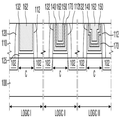
도 23은 본 발명의 제9 실시예에 따른 반도체 장치의 개념적인 레이아웃도이다. 도 24는 본 발명의 제9 실시예에 따른 반도체 장치의 단면도이다.23 is a conceptual layout diagram of a semiconductor device according to a ninth embodiment of the present invention. 24 is a cross-sectional view of a semiconductor device according to a ninth embodiment of the present invention.
도 23 및 도 24를 참조하면, 반도체 장치는 예를 들어, 메모리 영역(500)과 주변 영역(600)을 포함하는 메모리 장치일 수 있다. 이 때, 주변 영역(600)은 제1 내지 제3 로직 영역(610~630)을 포함할 수 있다.Referring to FIGS. 23 and 24, the semiconductor device may be, for example, a memory device including a
본 실시예에서, 제1 내지 제3 로직 영역(610~630)은 모두 예를 들어, PFET이 형성되는 영역일 수 있다.In the present embodiment, all of the first to
제1 로직 영역(610)에는 예를 들어, 도시된 것과 같이 도 1에 도시된 PFET 형성될 수 있고, 제2 로직 영역(620)에는 예를 들어, 도시된 것과 같이 도 7에 도시된 PFET 형성될 수 있으며, 제3 로직 영역(630)에는 예를 들어, 도시된 것과 같이 도 12에 도시된 PFET 형성될 수 있다. 하지만, 본 발명이 이에 제한되는 것은 아니며, 제1 내지 제3 로직 영역(610~630)에 형성되는 PFET의 형상은 필요에 따라 앞서 설명한 실시예들로 얼마든지 변형될 수 있다. In the
도 25는 본 발명의 실시예들에 따른 반도체 장치가 적용되는 전자 시스템의 블록도이다.25 is a block diagram of an electronic system to which a semiconductor device according to example embodiments of the inventive concepts is applied.
도 25를 참조하면, 전자 시스템(900)은 메모리 시스템(912), 프로세서(914), 램(916), 및 유저인터페이스(918)를 포함할 수 있다. 이러한 전자 시스템(900)의 예로는 모바일 기기나 컴퓨터 등을 들 수 있다. Referring to FIG. 25, the electronic system 900 may include a
메모리 시스템(912), 프로세서(914), 램(916), 및 유저인터페이스(918)는 버스(Bus, 920)를 이용하여 서로 데이터 통신을 할 수 있다. 프로세서(914)는 프로그램을 실행하고 전자 시스템(900)을 제어하는 역할을 할 수 있다. 램(916)은 프로세서(914)의 동작 메모리로서 사용될 수 있다. The
예를 들어, 프로세서(914), 램(916), 및/또는 메모리 시스템(912)은 각각 본 발명의 실시예들에 따른 반도체 장치를 포함할 수 있다. 그리고, 본 발명의 몇몇 실시예에서, 프로세서(914)와 램(916)은 하나의 패키지에 포함될 수도 있다. For example, the
유저 인터페이스(918)는 전자 시스템(900)에 데이터를 입력 또는 출력하는데 이용될 수 있다. 메모리 시스템(912)은 프로세서(914)의 동작을 위한 코드, 프로세서(914)에 의해 처리된 데이터 또는 외부에서 입력된 데이터를 저장할 수 있다. 메모리 시스템(912)은 제어기 및 메모리를 포함할 수도 있다.The
이상 첨부된 도면을 참조하여 본 발명의 실시예들을 설명하였으나, 본 발명은 상기 실시예들에 한정되는 것이 아니라 서로 다른 다양한 형태로 제조될 수 있으며, 본 발명이 속하는 기술분야에서 통상의 지식을 가진 자는 본 발명의 기술적 사상이나 필수적인 특징을 변경하지 않고서 다른 구체적인 형태로 실시될 수 있다는 것을 이해할 수 있을 것이다. 그러므로 이상에서 기술한 실시예들은 모든 면에서 예시적인 것이며 한정적이 아닌 것으로 이해해야만 한다.While the present invention has been described in connection with what is presently considered to be practical exemplary embodiments, it is to be understood that the invention is not limited to the disclosed embodiments, but, on the contrary, It is to be understood that the invention may be embodied in other specific forms without departing from the spirit or essential characteristics thereof. It is therefore to be understood that the above-described embodiments are illustrative in all aspects and not restrictive.
100: 반도체 기판 111, 112: 트렌치
130~132: 고유전율막 140: 확산막
150: 보호막 161, 162: 메탈 게이트 구조물
170: 확산 방지막100:
130 to 132: high dielectric constant film 140: diffusion film
150:
170: diffusion barrier
Claims (38)
상기 제1 및 제2 영역에 각각 형성된 제1 및 제2 트렌치;
상기 제1 및 제2 트렌치 내에 각각 형성된 제1 및 제2 고유전율(high-K)막;
상기 제1 고유전율막 상에 상기 제1 트렌치의 측벽을 따라 상부로 연장되어 형성된 확산막;
상기 확산막 상에 형성되고, 상기 확산막의 산화를 방지하는 방지하는 보호막;
상기 보호막 상에 형성된 제1 메탈 게이트 구조물; 및
상기 제2 고유전율막 상에 형성된 제2 메탈 게이트 구조물을 포함하는 반도체 장치.A semiconductor substrate including a first region and a second region;
First and second trenches respectively formed in the first and second regions;
First and second high-k films formed in the first and second trenches, respectively;
A diffusion film formed on the first high dielectric constant film and extending upward along a sidewall of the first trench;
A protective film formed on the diffusion film to prevent oxidation of the diffusion film;
A first metal gate structure formed on the passivation layer; And
And a second metal gate structure formed on the second high dielectric constant film.
상기 확산막은 메탈 산화막을 포함하는 반도체 장치.The method of claim 1,
The diffusion film includes a metal oxide film.
상기 메탈 산화막은 LaO, Y2O3, Lu2O3, SrO 중 적어도 하나를 포함하는 반도체 장치.The method of claim 2,
The metal oxide film includes at least one of LaO, Y 2 O 3, Lu 2 O 3, and SrO.
상기 보호막은 메탈 질화막을 포함하는 반도체 장치.The method of claim 1,
The protective film includes a metal nitride film.
상기 메탈 질화막은 TiN, TaN 중 적어도 하나를 포함하는 반도체 장치.5. The method of claim 4,
The metal nitride film includes at least one of TiN and TaN.
상기 제1 메탈 게이트 구조물과 상기 제2 메탈 게이트 구조물 중 적어도 어느 하나는 다층막 구조인 반도체 장치.The method of claim 1,
At least one of the first metal gate structure and the second metal gate structure is a semiconductor device.
상기 제1 메탈 게이트 구조물은 N타입 워크펑션(work function)막을 포함하고,
상기 제2 메탈 게이트 구조물은 P타입 워크펑션막을 포함하는 반도체 장치.The method according to claim 6,
The first metal gate structure includes an N type work function layer,
The second metal gate structure includes a P-type work function film.
상기 제1 메탈 게이트 구조물은 N타입 워크펑션막을 포함하고,
상기 제2 메탈 게이트 구조물은 하부 P타입 워크펑션막과 상부 N타입 워크펑션막을 포함하는 반도체 장치.The method according to claim 6,
The first metal gate structure includes an N type work function film,
The second metal gate structure includes a lower P-type work function layer and an upper N-type work function layer.
상기 제1 영역은 NFET 영역을 포함하고, 상기 제2 영역은 PFET 영역을 포함하는 반도체 장치.The method of claim 1,
Wherein the first region comprises an NFET region and the second region comprises a PFET region.
상기 제2 고유전율막 상에 형성된 확산 방지막을 더 포함하고,
상기 확산막은 상기 확산 방지막과 상기 제2 메탈 게이트 구조물 사이에 더 형성되는 반도체 장치.The method of claim 1,
Further comprising a diffusion barrier formed on the second high dielectric constant film,
The diffusion film is further formed between the diffusion barrier and the second metal gate structure.
상기 확산 방지막은 상기 확산막에 포함된 메탈이 상기 제2 고유전율막 및 상기 반도체 기판의 상기 제2 영역에 확산되는 것을 방지하는 반도체 장치.The method of claim 10,
The diffusion preventing film prevents the metal included in the diffusion film from diffusing into the second high dielectric constant film and the second region of the semiconductor substrate.
상기 확산 방지막은 메탈 질화막과 메탈을 포함하는 다층막 구조인 반도체 장치.The method of claim 10,
The diffusion barrier is a semiconductor device having a multi-layer film structure comprising a metal nitride film and a metal.
상기 메탈 질화막은 TiN을 포함하고,
상기 메탈은 Al을 포함하는 반도체 장치.13. The method of claim 12,
The metal nitride film includes TiN,
The metal includes Al.
상기 확산 방지막은 P타입 워크펑션막을 포함하는 반도체 장치.The method of claim 10,
The diffusion barrier layer includes a P type work function layer.
상기 제2 메탈 게이트 구조물 하부에 형성된 코발트막을 더 포함하는 반도체 장치.The method of claim 10,
And a cobalt film formed under the second metal gate structure.
상기 확산 방지막은 상기 제2 트렌치의 측벽을 따라 상부로 연장되어 형성되되, 그 상면이 상기 제2 트렌치의 상면보다 낮게 형성되는 반도체 장치.The method of claim 10,
The diffusion barrier layer is formed to extend upward along the sidewalls of the second trench, the upper surface of which is lower than the upper surface of the second trench.
상기 반도체 장치는 핀(fin)형 트랜지스터를 포함하는 반도체 장치.The method of claim 1,
The semiconductor device includes a fin transistor.
상기 반도체 기판 상에 형성되고 트렌치를 포함하는 층간 절연막;
상기 트렌치 내에 형성된 고유전율막;
상기 고유전율막 상에 상기 트렌치의 측벽을 따라 상부로 연장되어 형성된 제1 두께의 확산막;
상기 확산막 상에 형성되고, 상기 확산막의 산화를 방지하는 상기 제1 두께보다 큰 제2 두께의 보호막; 및
상기 보호막 상에 형성된 메탈 게이트 구조물을 포함하는 반도체 장치.A semiconductor substrate;
An interlayer insulating film formed on the semiconductor substrate and including a trench;
A high dielectric constant film formed in the trench;
A diffusion film having a first thickness formed on the high dielectric constant film and extending upward along the sidewalls of the trench;
A protective film having a second thickness greater than the first thickness formed on the diffusion film and preventing oxidation of the diffusion film; And
And a metal gate structure formed on the passivation layer.
상기 제1 두께는 3 내지 10Å이고,
상기 제2 두께는 11 내지 70Å인 반도체 장치.19. The method of claim 18,
The first thickness is 3 to 10Å,
And the second thickness is 11 to 70 GPa.
상기 메탈 게이트 구조물은 30 내지 120Å 두께의 N타입 워크펑션막을 포함하는 반도체 장치.19. The method of claim 18,
The metal gate structure includes an N-type work function film having a thickness of 30 to 120 microseconds.
상기 반도체 기판 상에 형성되고 트렌치를 포함하는 층간 절연막;
상기 트렌치 내에 형성된 고유전율막;
상기 고유전율막 상에 상기 트렌치의 측벽을 따라 상부로 연장되어 형성되되, 그 상면이 상기 트렌치의 상면보다 낮게 형성된 확산 방지막;
상기 확산 방지막 상에 상기 트렌치의 측벽을 따라 상부로 연장되어 형성된 확산막;
상기 확산막 상에 형성되고, 상기 확산막의 산화를 방지하는 보호막; 및
상기 보호막 상에 형성된 메탈 게이트 구조물을 포함하는 반도체 장치.A semiconductor substrate;
An interlayer insulating film formed on the semiconductor substrate and including a trench;
A high dielectric constant film formed in the trench;
A diffusion barrier layer formed on the high dielectric constant film and extending upward along the sidewalls of the trench, the diffusion barrier layer having an upper surface lower than an upper surface of the trench;
A diffusion film formed on the diffusion barrier layer and extending upward along a sidewall of the trench;
A protective film formed on the diffusion film and preventing oxidation of the diffusion film; And
And a metal gate structure formed on the passivation layer.
상기 확산 방지막의 두께는 1 내지 100Å이고,
상기 확산막의 두께는 3 내지 10Å이고,
상기 보호막의 두께는 11 내지 70Å인 반도체 장치.22. The method of claim 21,
The diffusion barrier has a thickness of 1 to 100Å,
The thickness of the diffusion film is 3 to 10Å,
The protective film has a thickness of 11 to 70 GPa.
상기 확산 방지막은 P타입 워크펑션막을 포함하고,
상기 메탈 게이트 구조물은 50 내지 100Å 두께의 N타입 워크펑션막을 포함하는 반도체 장치.22. The method of claim 21,
The diffusion barrier includes a P type work function film,
The metal gate structure includes an N-type work function film having a thickness of 50 to 100 microseconds.
상기 메모리 영역에 형성된 제1 및 제2 트렌치;
상기 로직 영역에 형성된 제3 트렌치;
상기 제1 내지 제3 트렌치 내에 각각 형성된 제1 내지 제3 고유전율(high-K)막;
상기 제1 고유전율막 상에 순차적으로 형성된 금속 산화막, 상기 금속 산화막의 산화를 방지하는 보호막, 및 제1 메탈 게이트 구조물;
상기 제2 고유전율막 상에 형성된 제2 메탈 게이트 구조물; 및
상기 제3 고유전율막 상에 순차적으로 형성된 확산 방지막, 상기 금속 산화막, 및 제3 메탈 게이트 구조물을 포함하는 반도체 장치.A semiconductor substrate including a memory region and a logic region;
First and second trenches formed in the memory area;
A third trench formed in the logic region;
First to third high dielectric constant (high-K) films respectively formed in the first to third trenches;
A metal oxide film sequentially formed on the first high dielectric constant film, a protective film to prevent oxidation of the metal oxide film, and a first metal gate structure;
A second metal gate structure formed on the second high dielectric constant film; And
A semiconductor device comprising a diffusion barrier layer, the metal oxide layer, and a third metal gate structure sequentially formed on the third high dielectric constant layer.
상기 제3 트렌치 내에 형성된 상기 확산 방지막은 상기 제3 트렌치의 측벽을 따라 상부로 연장되어 형성되되, 그 상면이 상기 제3 트렌치의 상면보다 낮게 형성되는 반도체 장치.25. The method of claim 24,
The diffusion barrier formed in the third trench extends upwardly along the sidewalls of the third trench, the upper surface of which is lower than the upper surface of the third trench.
상기 메모리 영역은 SRAM 영역을 포함하는 반도체 장치.25. The method of claim 24,
And the memory area comprises an SRAM area.
상기 제1 및 제2 트렌치 내에 각각 고유전율막을 형성하고,
상기 고유전율막 상에 확산막 및 상기 확산막의 산화를 방지하는 보호막을 순차적으로 형성하고,
상기 반도체 기판을 열처리하여 상기 제1 트렌치 내에 형성된 상기 확산막에 포함된 물질을 상기 제1 트렌치 내에 형성된 상기 고유전율막과 상기 제1 영역의 반도체 기판에 확산시키고,
상기 제1 트렌치 내에 형성된 보호막 상에 제1 메탈 게이트 구조물을 형성하고,
상기 제2 트렌치 내에 형성된 고유전율막 상에 제2 메탈 게이트 구조물을 형성하는 것을 포함하는 반도체 장치의 제조 방법.Preparing a semiconductor substrate including a first region and a second region, and first and second trenches formed in the first and second regions, respectively,
Forming a high dielectric constant film in each of the first and second trenches,
Sequentially forming a diffusion film and a protective film on the high dielectric film to prevent oxidation of the diffusion film,
Heat treating the semiconductor substrate to diffuse a material included in the diffusion film formed in the first trench into the high dielectric constant film formed in the first trench and the semiconductor substrate of the first region;
Forming a first metal gate structure on the passivation layer formed in the first trench,
And forming a second metal gate structure on the high dielectric constant film formed in the second trench.
상기 확산막에 포함된 물질은 상기 확산막에 포함된 메탈을 포함하는 반도체 장치의 제조 방법.28. The method of claim 27,
The material included in the diffusion film includes a metal included in the diffusion film.
상기 확산막은 LaO를 포함하고,
상기 메탈은 La를 포함하는 반도체 장치의 제조 방법.29. The method of claim 28,
The diffusion film includes LaO,
The metal is a manufacturing method of a semiconductor device containing La.
상기 반도체 기판을 열처리 시, 상기 확산막 상에는 폴리 실리콘막이 형성되는 반도체 장치의 제조 방법.28. The method of claim 27,
And a polysilicon film is formed on the diffusion film when the semiconductor substrate is heat treated.
상기 반도체 기판을 열처리 시, 확산막은 외부로 노출되는 반도체 장치의 제조 방법.28. The method of claim 27,
The diffusion film is exposed to the outside when the semiconductor substrate is heat treated.
상기 제2 트렌치 내에 형성된 상기 확산막과 보호막을 제거하는 것을 더 포함하는 반도체 장치의 제조 방법.28. The method of claim 27,
Removing the diffusion film and the protective film formed in the second trench.
상기 고유전율막 상에 상기 확산막 및 상기 보호막을 순차적으로 형성하기 전,
상기 제2 트렌치 내에 형성된 상기 고유전율막 상에 확산 방지막을 형성하는 것을 더 포함하는 반도체 장치의 제조 방법.28. The method of claim 27,
Before sequentially forming the diffusion film and the protective film on the high dielectric constant film,
And forming a diffusion barrier film on the high dielectric constant film formed in the second trench.
상기 확산 방지막은 워크펑션막을 포함하는 반도체 장치의 제조 방법.34. The method of claim 33,
The diffusion barrier layer includes a work function layer.
상기 워크펑션막은 P타입 워크펑션막을 포함하는 반도체 장치의 제조 방법.35. The method of claim 34,
The work function film includes a P type work function film.
상기 제2 메탈 게이트 구조물을 형성하기 전, 코발트막을 형성하는 것을 더 포함하는 반도체 장치의 제조 방법.34. The method of claim 33,
And forming a cobalt film before forming the second metal gate structure.
상기 코발트막은 CVD 방식으로 형성하는 반도체 장치의 제조 방법.37. The method of claim 36,
The cobalt film is formed by a CVD method.
상기 제1 및 제2 트렌치를 준비하는 것은,
상기 반도체 기판의 제1 및 제2 영역 상에, 각각 더미(dummy) 게이트를 형성하고,
상기 더미 게이트를 덮도록 층간 절연막을 형성하고,
상기 층간 절연막을 평탄화하여 상기 더미 게이트를 노출시키고,
상기 노출된 더미 게이트를 제거하여 상기 제1 및 제2 영역에 각각 상기 제1 및 제2 트렌치를 형성하는 것을 포함하는 반도체 장치의 제조 방법.28. The method of claim 27,
Preparing the first and second trenches,
Forming dummy gates on the first and second regions of the semiconductor substrate,
An interlayer insulating film is formed to cover the dummy gate,
Planarizing the interlayer insulating film to expose the dummy gate,
Removing the exposed dummy gate to form the first and second trenches in the first and second regions, respectively.
Priority Applications (5)
| Application Number | Priority Date | Filing Date | Title |
|---|---|---|---|
| KR20120051036A KR20130127257A (en) | 2012-05-14 | 2012-05-14 | Semiconductor device and method for manufacturing the device |
| US13/733,936 US8969878B2 (en) | 2012-05-14 | 2013-01-04 | Semiconductor device and method for manufacturing the device |
| TW102115476A TWI590456B (en) | 2012-05-14 | 2013-04-30 | Semiconductor device and method for manufacturing the device |
| CN201310176515.2A CN103426928B (en) | 2012-05-14 | 2013-05-14 | The manufacturing method of semiconductor devices and the device |
| US14/576,268 US20150102418A1 (en) | 2012-05-14 | 2014-12-19 | Semiconductor device and method for manufacturing the device |
Applications Claiming Priority (1)
| Application Number | Priority Date | Filing Date | Title |
|---|---|---|---|
| KR20120051036A KR20130127257A (en) | 2012-05-14 | 2012-05-14 | Semiconductor device and method for manufacturing the device |
Publications (1)
| Publication Number | Publication Date |
|---|---|
| KR20130127257A true KR20130127257A (en) | 2013-11-22 |
Family
ID=49547991
Family Applications (1)
| Application Number | Title | Priority Date | Filing Date |
|---|---|---|---|
| KR20120051036A KR20130127257A (en) | 2012-05-14 | 2012-05-14 | Semiconductor device and method for manufacturing the device |
Country Status (4)
| Country | Link |
|---|---|
| US (2) | US8969878B2 (en) |
| KR (1) | KR20130127257A (en) |
| CN (1) | CN103426928B (en) |
| TW (1) | TWI590456B (en) |
Cited By (6)
| Publication number | Priority date | Publication date | Assignee | Title |
|---|---|---|---|---|
| KR20150077545A (en) * | 2013-12-27 | 2015-07-08 | 삼성전자주식회사 | Semiconductor package and method for fabricating the same |
| KR20160093424A (en) * | 2015-01-29 | 2016-08-08 | 삼성전자주식회사 | Semiconductor device having work-function metal and method of forming the same |
| KR20180104476A (en) * | 2017-03-13 | 2018-09-21 | 삼성전자주식회사 | Semiconductor device and method for fabricating the same |
| US10468407B2 (en) | 2015-05-15 | 2019-11-05 | Taiwan Semiconductor Manufacturing Co., Ltd. | Fin field effect transistor (FinFET) device structure with uneven gate structure |
| KR20200049505A (en) * | 2018-10-26 | 2020-05-08 | 타이완 세미콘덕터 매뉴팩쳐링 컴퍼니 리미티드 | Gate structures having interfacial layers |
| KR20210146774A (en) * | 2020-05-26 | 2021-12-06 | 타이완 세미콘덕터 매뉴팩쳐링 컴퍼니 리미티드 | Gate structures for semiconductor devices |
Families Citing this family (47)
| Publication number | Priority date | Publication date | Assignee | Title |
|---|---|---|---|---|
| US9018711B1 (en) * | 2013-10-17 | 2015-04-28 | Globalfoundries Inc. | Selective growth of a work-function metal in a replacement metal gate of a semiconductor device |
| CN104752316B (en) * | 2013-12-25 | 2018-03-20 | 中芯国际集成电路制造(上海)有限公司 | A kind of method for making semiconductor devices |
| US9236397B2 (en) * | 2014-02-04 | 2016-01-12 | Globalfoundries Inc. | FinFET device containing a composite spacer structure |
| US9362180B2 (en) | 2014-02-25 | 2016-06-07 | Globalfoundries Inc. | Integrated circuit having multiple threshold voltages |
| US9455201B2 (en) * | 2014-02-25 | 2016-09-27 | Globalfoundries Inc. | Integration method for fabrication of metal gate based multiple threshold voltage devices and circuits |
| US9698019B2 (en) | 2014-03-14 | 2017-07-04 | Taiwan Semiconductor Manufacturing Company, Ltd. | N-work function metal with crystal structure |
| KR102212267B1 (en) * | 2014-03-19 | 2021-02-04 | 삼성전자주식회사 | Semiconductor device and method for fabricating the same |
| US9401362B2 (en) | 2014-04-04 | 2016-07-26 | Globalfoundries Inc. | Multiple threshold voltage semiconductor device |
| US9570319B2 (en) * | 2014-05-30 | 2017-02-14 | Taiwan Semiconductor Manufacturing Company, Ltd. | Method of manufacturing a semiconductor device |
| KR102127644B1 (en) | 2014-06-10 | 2020-06-30 | 삼성전자 주식회사 | Method for fabricating semiconductor device |
| TWI653762B (en) | 2014-10-08 | 2019-03-11 | 聯華電子股份有限公司 | Semiconductor device having metal gate and method for manufacturing the same |
| US10910481B2 (en) * | 2014-11-05 | 2021-02-02 | Cree, Inc. | Semiconductor device with improved insulated gate |
| US9466494B2 (en) * | 2014-11-18 | 2016-10-11 | Taiwan Semiconductor Manufacturing Company, Ltd. | Selective growth for high-aspect ration metal fill |
| CN105826260B (en) * | 2015-01-08 | 2019-01-22 | 中芯国际集成电路制造(上海)有限公司 | The forming method of semiconductor devices |
| CN105826258B (en) * | 2015-01-08 | 2018-10-16 | 中芯国际集成电路制造(上海)有限公司 | The forming method of semiconductor devices |
| TWI575581B (en) * | 2015-04-14 | 2017-03-21 | 格羅方德半導體公司 | Selective growth of a work-function metal in a replacement metal gate of a semiconductor device |
| US10062618B2 (en) * | 2015-05-26 | 2018-08-28 | GlobalFoundries, Inc. | Method and structure for formation of replacement metal gate field effect transistors |
| KR102290685B1 (en) * | 2015-06-04 | 2021-08-17 | 삼성전자주식회사 | Semiconductor device |
| US9570318B1 (en) | 2015-07-22 | 2017-02-14 | International Business Machines Corporation | High-k and p-type work function metal first fabrication process having improved annealing process flows |
| US10164059B2 (en) | 2015-09-04 | 2018-12-25 | Taiwan Semiconductor Manufacturing Co., Ltd. | FinFET device and fabricating method thereof |
| US9685510B2 (en) | 2015-09-10 | 2017-06-20 | International Business Machines Corporation | SiGe CMOS with tensely strained NFET and compressively strained PFET |
| CN106601605B (en) * | 2015-10-19 | 2020-02-28 | 中芯国际集成电路制造(北京)有限公司 | Gate stack structure, NMOS device, semiconductor device and manufacturing method thereof |
| CN106601606B (en) * | 2015-10-19 | 2019-09-20 | 中芯国际集成电路制造(上海)有限公司 | NMOS device, semiconductor device and its manufacturing method |
| US9673331B2 (en) | 2015-11-02 | 2017-06-06 | Taiwan Semiconductor Manufacturing Company, Ltd. | Structure and formation method of semiconductor device structure |
| US10020304B2 (en) * | 2015-11-16 | 2018-07-10 | Taiwan Semiconductor Manufacturing Co., Ltd. | Fin field effect transistor, semiconductor device and fabricating method thereof |
| US10079182B2 (en) * | 2016-01-15 | 2018-09-18 | International Business Machines Corporation | Field effect transistor gate stack |
| US9985031B2 (en) * | 2016-01-21 | 2018-05-29 | Taiwan Semiconductor Manufacturing Co., Ltd. | Integrated circuit and manufacturing method thereof |
| US10056301B2 (en) * | 2016-06-20 | 2018-08-21 | Semiconductor Manufacturing International (Shanghai) Corporation | Transistor and fabrication method thereof |
| US10128237B2 (en) * | 2016-06-24 | 2018-11-13 | Taiwan Semiconductor Manufacturing Co., Ltd. | Methods of gate replacement in semiconductor devices |
| US9991362B2 (en) * | 2016-09-30 | 2018-06-05 | Taiwan Semiconductor Manufacturing Co., Ltd. | Semiconductor device including tungsten gate and manufacturing method thereof |
| US9881930B1 (en) * | 2016-10-21 | 2018-01-30 | International Business Machines Corporation | Simple integration of non-volatile memory and complementary metal oxide semiconductor |
| KR102342550B1 (en) * | 2017-06-09 | 2021-12-23 | 삼성전자주식회사 | Semiconductor devices |
| CN107527805B (en) * | 2017-08-31 | 2018-11-06 | 长江存储科技有限责任公司 | A kind of metal gate structure and forming method thereof |
| KR102316293B1 (en) * | 2017-09-18 | 2021-10-22 | 삼성전자주식회사 | Semiconductor devices |
| US10367078B2 (en) * | 2017-11-09 | 2019-07-30 | Taiwan Semiconductor Manufacturing Co., Ltd. | Semiconductor devices and FinFET devices having shielding layers |
| US10629749B2 (en) | 2017-11-30 | 2020-04-21 | Taiwan Semiconductor Manufacturing Co., Ltd. | Method of treating interfacial layer on silicon germanium |
| CN108777261A (en) * | 2018-06-07 | 2018-11-09 | 上海华力集成电路制造有限公司 | A kind of gate structure and its manufacturing method of transistor |
| KR102560695B1 (en) * | 2018-09-05 | 2023-07-27 | 삼성전자주식회사 | Integrated circuit devices |
| US11329042B2 (en) | 2018-11-30 | 2022-05-10 | Taiwan Semiconductor Manufacturing Co., Ltd. | Gate structures having neutral zones to minimize metal gate boundary effects and methods of fabricating thereof |
| TWI727505B (en) * | 2018-11-30 | 2021-05-11 | 台灣積體電路製造股份有限公司 | Integrated circuit device and fabricating method thereof |
| US11127857B2 (en) * | 2019-04-12 | 2021-09-21 | Taiwan Semiconductor Manufacturing Company, Ltd. | Semiconductor device and method of manufacture |
| US11164868B2 (en) * | 2019-09-24 | 2021-11-02 | Taiwan Semiconductor Manufacturing Company, Ltd. | Semiconductor device |
| TWI755874B (en) | 2019-09-30 | 2022-02-21 | 台灣積體電路製造股份有限公司 | Semiconductor device and forming method thereof |
| US11367479B2 (en) | 2019-09-30 | 2022-06-21 | Taiwan Semiconductor Manufacturing Co., Ltd. | SRAM structure and method |
| US20210118874A1 (en) * | 2019-10-21 | 2021-04-22 | Nanya Technology Corporation | Semiconductor device and method for fabricating the same |
| US20210202321A1 (en) * | 2019-12-30 | 2021-07-01 | Taiwan Semiconductor Manufacturing Co., Ltd. | High Voltage Devices |
| CN114765130A (en) * | 2021-01-11 | 2022-07-19 | 长鑫存储技术有限公司 | Semiconductor structure manufacturing method and semiconductor structure |
Family Cites Families (21)
| Publication number | Priority date | Publication date | Assignee | Title |
|---|---|---|---|---|
| US6528856B1 (en) * | 1998-12-15 | 2003-03-04 | Intel Corporation | High dielectric constant metal oxide gate dielectrics |
| US6271094B1 (en) * | 2000-02-14 | 2001-08-07 | International Business Machines Corporation | Method of making MOSFET with high dielectric constant gate insulator and minimum overlap capacitance |
| JP2001284466A (en) | 2000-03-29 | 2001-10-12 | Matsushita Electric Ind Co Ltd | Semiconductor device and method of manufacturing it |
| JP2002198441A (en) | 2000-11-16 | 2002-07-12 | Hynix Semiconductor Inc | Method for forming dual metal gate of semiconductor element |
| KR100386034B1 (en) * | 2000-12-06 | 2003-06-02 | 에이에스엠 마이크로케미스트리 리미티드 | Method of Fabricating Semiconductor Device Employing Copper Interconnect Structure Having Diffusion Barrier Stuffed with Metal Oxide |
| US7952118B2 (en) * | 2003-11-12 | 2011-05-31 | Samsung Electronics Co., Ltd. | Semiconductor device having different metal gate structures |
| US7390709B2 (en) | 2004-09-08 | 2008-06-24 | Intel Corporation | Method for making a semiconductor device having a high-k gate dielectric layer and a metal gate electrode |
| US7126199B2 (en) * | 2004-09-27 | 2006-10-24 | Intel Corporation | Multilayer metal gate electrode |
| US7902058B2 (en) | 2004-09-29 | 2011-03-08 | Intel Corporation | Inducing strain in the channels of metal gate transistors |
| US8101485B2 (en) | 2005-12-16 | 2012-01-24 | Intel Corporation | Replacement gates to enhance transistor strain |
| EP1845554A3 (en) * | 2006-04-10 | 2011-07-13 | Imec | A method to create super secondary grain growth in narrow trenches |
| US7888195B2 (en) * | 2008-08-26 | 2011-02-15 | United Microelectronics Corp. | Metal gate transistor and method for fabricating the same |
| KR101486425B1 (en) * | 2008-11-19 | 2015-01-27 | 삼성전자주식회사 | Method of fabricating semiconductor device having dual gate |
| US8304841B2 (en) * | 2009-09-14 | 2012-11-06 | Taiwan Semiconductor Manufacturing Company, Ltd. | Metal gate transistor, integrated circuits, systems, and fabrication methods thereof |
| CN102110650A (en) | 2009-12-29 | 2011-06-29 | 中国科学院微电子研究所 | Semiconductor device and manufacturing method thereof |
| US8330227B2 (en) | 2010-02-17 | 2012-12-11 | Taiwan Semiconductor Manufacturing Company, Ltd. | Integrated semiconductor structure for SRAM and fabrication methods thereof |
| US8232148B2 (en) | 2010-03-04 | 2012-07-31 | International Business Machines Corporation | Structure and method to make replacement metal gate and contact metal |
| US9312260B2 (en) * | 2010-05-26 | 2016-04-12 | Taiwan Semiconductor Manufacturing Company, Ltd. | Integrated circuits and manufacturing methods thereof |
| KR101674398B1 (en) * | 2010-08-03 | 2016-11-10 | 삼성전자주식회사 | Semiconductor devices and methods of manufacturing the same |
| US9755039B2 (en) * | 2011-07-28 | 2017-09-05 | Taiwan Semiconductor Manufacturing Company, Ltd. | Semiconductor device having a metal gate electrode stack |
| US8951855B2 (en) * | 2012-04-24 | 2015-02-10 | United Microelectronics Corp. | Manufacturing method for semiconductor device having metal gate |
-
2012
- 2012-05-14 KR KR20120051036A patent/KR20130127257A/en not_active Application Discontinuation
-
2013
- 2013-01-04 US US13/733,936 patent/US8969878B2/en active Active
- 2013-04-30 TW TW102115476A patent/TWI590456B/en active
- 2013-05-14 CN CN201310176515.2A patent/CN103426928B/en active Active
-
2014
- 2014-12-19 US US14/576,268 patent/US20150102418A1/en not_active Abandoned
Cited By (11)
| Publication number | Priority date | Publication date | Assignee | Title |
|---|---|---|---|---|
| KR20150077545A (en) * | 2013-12-27 | 2015-07-08 | 삼성전자주식회사 | Semiconductor package and method for fabricating the same |
| KR20160093424A (en) * | 2015-01-29 | 2016-08-08 | 삼성전자주식회사 | Semiconductor device having work-function metal and method of forming the same |
| US11043430B2 (en) | 2015-01-29 | 2021-06-22 | Samsung Electronics Co., Ltd. | Semiconductor device having work-function metal and method of forming the same |
| US11462442B2 (en) | 2015-01-29 | 2022-10-04 | Samsung Electronics Co., Ltd. | Semiconductor device having work-function metal and method of forming the same |
| US11929289B2 (en) | 2015-01-29 | 2024-03-12 | Samsung Electronics Co., Ltd. | Semiconductor device having work-function metal and method of forming the same |
| US10468407B2 (en) | 2015-05-15 | 2019-11-05 | Taiwan Semiconductor Manufacturing Co., Ltd. | Fin field effect transistor (FinFET) device structure with uneven gate structure |
| US11139295B2 (en) | 2015-05-22 | 2021-10-05 | Taiwan Semiconductor Manufacturing Co., Ltd. | Fin field effect transistor (FinFET) device and method |
| KR20180104476A (en) * | 2017-03-13 | 2018-09-21 | 삼성전자주식회사 | Semiconductor device and method for fabricating the same |
| KR20200049505A (en) * | 2018-10-26 | 2020-05-08 | 타이완 세미콘덕터 매뉴팩쳐링 컴퍼니 리미티드 | Gate structures having interfacial layers |
| US10985022B2 (en) | 2018-10-26 | 2021-04-20 | Taiwan Semiconductor Manufacturing Co., Ltd. | Gate structures having interfacial layers |
| KR20210146774A (en) * | 2020-05-26 | 2021-12-06 | 타이완 세미콘덕터 매뉴팩쳐링 컴퍼니 리미티드 | Gate structures for semiconductor devices |
Also Published As
| Publication number | Publication date |
|---|---|
| US20130299914A1 (en) | 2013-11-14 |
| TW201347194A (en) | 2013-11-16 |
| CN103426928B (en) | 2018-06-08 |
| US8969878B2 (en) | 2015-03-03 |
| US20150102418A1 (en) | 2015-04-16 |
| CN103426928A (en) | 2013-12-04 |
| TWI590456B (en) | 2017-07-01 |
Similar Documents
| Publication | Publication Date | Title |
|---|---|---|
| KR20130127257A (en) | Semiconductor device and method for manufacturing the device | |
| US11322577B2 (en) | Negative capacitance FET with improved reliability performance | |
| US9337057B2 (en) | Semiconductor device and method for fabricating the same | |
| US9287181B2 (en) | Semiconductor device and method for fabricating the same | |
| US9318335B2 (en) | Method for fabricating semiconductor device including nitrided gate insulator | |
| US9899270B2 (en) | Methods for manufacturing semiconductor devices | |
| KR20140034347A (en) | Semiconductor device and method for fabricating the same | |
| KR20130123158A (en) | Method for manufacturing semiconductor device | |
| US10395080B2 (en) | Simplified gate stack process to improve dual channel CMOS performance | |
| CN103311247A (en) | Semiconductor device and manufacturing method thereof | |
| KR20140148189A (en) | Semiconductor device and method for fabricating the same | |
| CN104051460A (en) | Semiconductor device including dummy isolation gate structure and method of fabricating thereof | |
| US20170025526A1 (en) | High-k and p-type work function metal first fabrication process having improved annealing process flows | |
| US9653462B2 (en) | Semiconductor device and method for fabricating the same | |
| CN103094214B (en) | Manufacturing method for semiconductor device | |
| US20080142910A1 (en) | Semiconductor device | |
| US20140312387A1 (en) | Semiconductor device and method for fabricating the same | |
| KR20170009672A (en) | Semiconductor device and method for fabricating the same | |
| KR101974439B1 (en) | Semiconductor device and fabricated method thereof | |
| US8735994B2 (en) | Electrical-free dummy gate | |
| US20220199808A1 (en) | Semiconductor structure and method for forming the same | |
| KR20150049129A (en) | Semiconductor device and method for fabricating the same | |
| CN109671673B (en) | Semiconductor structure and forming method thereof | |
| KR20130127261A (en) | Semiconductor device and the fabricating method thereof | |
| KR20110077844A (en) | Method for manufacturing cmos transistor |
Legal Events
| Date | Code | Title | Description |
|---|---|---|---|
| WITN | Application deemed withdrawn, e.g. because no request for examination was filed or no examination fee was paid |