KR20130108574A - Array substrate, manufacturing method thereof, and display device - Google Patents
Array substrate, manufacturing method thereof, and display device Download PDFInfo
- Publication number
- KR20130108574A KR20130108574A KR1020137008359A KR20137008359A KR20130108574A KR 20130108574 A KR20130108574 A KR 20130108574A KR 1020137008359 A KR1020137008359 A KR 1020137008359A KR 20137008359 A KR20137008359 A KR 20137008359A KR 20130108574 A KR20130108574 A KR 20130108574A
- Authority
- KR
- South Korea
- Prior art keywords
- electrode
- layer
- region
- array substrate
- insulating layer
- Prior art date
Links
- 239000000758 substrate Substances 0.000 title claims abstract description 59
- 238000004519 manufacturing process Methods 0.000 title claims abstract description 14
- 229920005989 resin Polymers 0.000 claims abstract description 35
- 239000011347 resin Substances 0.000 claims abstract description 35
- 239000010409 thin film Substances 0.000 claims abstract description 27
- 238000002161 passivation Methods 0.000 claims abstract description 25
- 230000005684 electric field Effects 0.000 claims abstract description 11
- 239000010410 layer Substances 0.000 claims description 139
- 238000000034 method Methods 0.000 claims description 26
- 238000003860 storage Methods 0.000 claims description 20
- 239000003990 capacitor Substances 0.000 claims description 18
- 239000007769 metal material Substances 0.000 claims description 18
- 239000011241 protective layer Substances 0.000 claims description 15
- 239000011159 matrix material Substances 0.000 claims description 11
- 229910052751 metal Inorganic materials 0.000 claims description 10
- 239000002184 metal Substances 0.000 claims description 10
- 239000011810 insulating material Substances 0.000 claims description 5
- 239000004973 liquid crystal related substance Substances 0.000 description 24
- 230000008569 process Effects 0.000 description 15
- 239000000463 material Substances 0.000 description 13
- 238000000059 patterning Methods 0.000 description 12
- 238000000151 deposition Methods 0.000 description 5
- 230000000694 effects Effects 0.000 description 5
- 239000004020 conductor Substances 0.000 description 4
- 239000004065 semiconductor Substances 0.000 description 4
- 238000010586 diagram Methods 0.000 description 3
- 230000001788 irregular Effects 0.000 description 3
- 238000002834 transmittance Methods 0.000 description 3
- 229910004205 SiNX Inorganic materials 0.000 description 2
- 229910021417 amorphous silicon Inorganic materials 0.000 description 2
- 210000004027 cell Anatomy 0.000 description 2
- 239000000975 dye Substances 0.000 description 2
- NIXOWILDQLNWCW-UHFFFAOYSA-M Acrylate Chemical compound [O-]C(=O)C=C NIXOWILDQLNWCW-UHFFFAOYSA-M 0.000 description 1
- 239000004642 Polyimide Substances 0.000 description 1
- 230000002159 abnormal effect Effects 0.000 description 1
- 229910045601 alloy Inorganic materials 0.000 description 1
- 239000000956 alloy Substances 0.000 description 1
- 230000004075 alteration Effects 0.000 description 1
- 229910052782 aluminium Inorganic materials 0.000 description 1
- 230000005540 biological transmission Effects 0.000 description 1
- 239000003086 colorant Substances 0.000 description 1
- 229910052802 copper Inorganic materials 0.000 description 1
- 210000002858 crystal cell Anatomy 0.000 description 1
- 230000000593 degrading effect Effects 0.000 description 1
- 239000003822 epoxy resin Substances 0.000 description 1
- 238000005530 etching Methods 0.000 description 1
- 239000011521 glass Substances 0.000 description 1
- AMGQUBHHOARCQH-UHFFFAOYSA-N indium;oxotin Chemical compound [In].[Sn]=O AMGQUBHHOARCQH-UHFFFAOYSA-N 0.000 description 1
- 238000009413 insulation Methods 0.000 description 1
- 239000011229 interlayer Substances 0.000 description 1
- 238000012986 modification Methods 0.000 description 1
- 230000004048 modification Effects 0.000 description 1
- 229910052750 molybdenum Inorganic materials 0.000 description 1
- 230000003287 optical effect Effects 0.000 description 1
- 229920000647 polyepoxide Polymers 0.000 description 1
- 229920001721 polyimide Polymers 0.000 description 1
- 230000005855 radiation Effects 0.000 description 1
- 230000004044 response Effects 0.000 description 1
- 229910052814 silicon oxide Inorganic materials 0.000 description 1
- 229910052719 titanium Inorganic materials 0.000 description 1
- 238000001039 wet etching Methods 0.000 description 1
- YVTHLONGBIQYBO-UHFFFAOYSA-N zinc indium(3+) oxygen(2-) Chemical compound [O--].[Zn++].[In+3] YVTHLONGBIQYBO-UHFFFAOYSA-N 0.000 description 1
Images

Classifications
-
- G—PHYSICS
- G02—OPTICS
- G02F—OPTICAL DEVICES OR ARRANGEMENTS FOR THE CONTROL OF LIGHT BY MODIFICATION OF THE OPTICAL PROPERTIES OF THE MEDIA OF THE ELEMENTS INVOLVED THEREIN; NON-LINEAR OPTICS; FREQUENCY-CHANGING OF LIGHT; OPTICAL LOGIC ELEMENTS; OPTICAL ANALOGUE/DIGITAL CONVERTERS
- G02F1/00—Devices or arrangements for the control of the intensity, colour, phase, polarisation or direction of light arriving from an independent light source, e.g. switching, gating or modulating; Non-linear optics
- G02F1/01—Devices or arrangements for the control of the intensity, colour, phase, polarisation or direction of light arriving from an independent light source, e.g. switching, gating or modulating; Non-linear optics for the control of the intensity, phase, polarisation or colour
- G02F1/13—Devices or arrangements for the control of the intensity, colour, phase, polarisation or direction of light arriving from an independent light source, e.g. switching, gating or modulating; Non-linear optics for the control of the intensity, phase, polarisation or colour based on liquid crystals, e.g. single liquid crystal display cells
- G02F1/133—Constructional arrangements; Operation of liquid crystal cells; Circuit arrangements
- G02F1/1333—Constructional arrangements; Manufacturing methods
- G02F1/1343—Electrodes
-
- H—ELECTRICITY
- H01—ELECTRIC ELEMENTS
- H01L—SEMICONDUCTOR DEVICES NOT COVERED BY CLASS H10
- H01L27/00—Devices consisting of a plurality of semiconductor or other solid-state components formed in or on a common substrate
- H01L27/02—Devices consisting of a plurality of semiconductor or other solid-state components formed in or on a common substrate including semiconductor components specially adapted for rectifying, oscillating, amplifying or switching and having potential barriers; including integrated passive circuit elements having potential barriers
- H01L27/12—Devices consisting of a plurality of semiconductor or other solid-state components formed in or on a common substrate including semiconductor components specially adapted for rectifying, oscillating, amplifying or switching and having potential barriers; including integrated passive circuit elements having potential barriers the substrate being other than a semiconductor body, e.g. an insulating body
- H01L27/1214—Devices consisting of a plurality of semiconductor or other solid-state components formed in or on a common substrate including semiconductor components specially adapted for rectifying, oscillating, amplifying or switching and having potential barriers; including integrated passive circuit elements having potential barriers the substrate being other than a semiconductor body, e.g. an insulating body comprising a plurality of TFTs formed on a non-semiconducting substrate, e.g. driving circuits for AMLCDs
- H01L27/124—Devices consisting of a plurality of semiconductor or other solid-state components formed in or on a common substrate including semiconductor components specially adapted for rectifying, oscillating, amplifying or switching and having potential barriers; including integrated passive circuit elements having potential barriers the substrate being other than a semiconductor body, e.g. an insulating body comprising a plurality of TFTs formed on a non-semiconducting substrate, e.g. driving circuits for AMLCDs with a particular composition, shape or layout of the wiring layers specially adapted to the circuit arrangement, e.g. scanning lines in LCD pixel circuits
-
- G—PHYSICS
- G02—OPTICS
- G02F—OPTICAL DEVICES OR ARRANGEMENTS FOR THE CONTROL OF LIGHT BY MODIFICATION OF THE OPTICAL PROPERTIES OF THE MEDIA OF THE ELEMENTS INVOLVED THEREIN; NON-LINEAR OPTICS; FREQUENCY-CHANGING OF LIGHT; OPTICAL LOGIC ELEMENTS; OPTICAL ANALOGUE/DIGITAL CONVERTERS
- G02F1/00—Devices or arrangements for the control of the intensity, colour, phase, polarisation or direction of light arriving from an independent light source, e.g. switching, gating or modulating; Non-linear optics
- G02F1/01—Devices or arrangements for the control of the intensity, colour, phase, polarisation or direction of light arriving from an independent light source, e.g. switching, gating or modulating; Non-linear optics for the control of the intensity, phase, polarisation or colour
- G02F1/13—Devices or arrangements for the control of the intensity, colour, phase, polarisation or direction of light arriving from an independent light source, e.g. switching, gating or modulating; Non-linear optics for the control of the intensity, phase, polarisation or colour based on liquid crystals, e.g. single liquid crystal display cells
- G02F1/133—Constructional arrangements; Operation of liquid crystal cells; Circuit arrangements
- G02F1/136—Liquid crystal cells structurally associated with a semi-conducting layer or substrate, e.g. cells forming part of an integrated circuit
- G02F1/1362—Active matrix addressed cells
- G02F1/1368—Active matrix addressed cells in which the switching element is a three-electrode device
-
- H—ELECTRICITY
- H01—ELECTRIC ELEMENTS
- H01L—SEMICONDUCTOR DEVICES NOT COVERED BY CLASS H10
- H01L27/00—Devices consisting of a plurality of semiconductor or other solid-state components formed in or on a common substrate
- H01L27/02—Devices consisting of a plurality of semiconductor or other solid-state components formed in or on a common substrate including semiconductor components specially adapted for rectifying, oscillating, amplifying or switching and having potential barriers; including integrated passive circuit elements having potential barriers
- H01L27/12—Devices consisting of a plurality of semiconductor or other solid-state components formed in or on a common substrate including semiconductor components specially adapted for rectifying, oscillating, amplifying or switching and having potential barriers; including integrated passive circuit elements having potential barriers the substrate being other than a semiconductor body, e.g. an insulating body
- H01L27/1214—Devices consisting of a plurality of semiconductor or other solid-state components formed in or on a common substrate including semiconductor components specially adapted for rectifying, oscillating, amplifying or switching and having potential barriers; including integrated passive circuit elements having potential barriers the substrate being other than a semiconductor body, e.g. an insulating body comprising a plurality of TFTs formed on a non-semiconducting substrate, e.g. driving circuits for AMLCDs
- H01L27/1259—Multistep manufacturing methods
-
- G—PHYSICS
- G02—OPTICS
- G02F—OPTICAL DEVICES OR ARRANGEMENTS FOR THE CONTROL OF LIGHT BY MODIFICATION OF THE OPTICAL PROPERTIES OF THE MEDIA OF THE ELEMENTS INVOLVED THEREIN; NON-LINEAR OPTICS; FREQUENCY-CHANGING OF LIGHT; OPTICAL LOGIC ELEMENTS; OPTICAL ANALOGUE/DIGITAL CONVERTERS
- G02F1/00—Devices or arrangements for the control of the intensity, colour, phase, polarisation or direction of light arriving from an independent light source, e.g. switching, gating or modulating; Non-linear optics
- G02F1/01—Devices or arrangements for the control of the intensity, colour, phase, polarisation or direction of light arriving from an independent light source, e.g. switching, gating or modulating; Non-linear optics for the control of the intensity, phase, polarisation or colour
- G02F1/13—Devices or arrangements for the control of the intensity, colour, phase, polarisation or direction of light arriving from an independent light source, e.g. switching, gating or modulating; Non-linear optics for the control of the intensity, phase, polarisation or colour based on liquid crystals, e.g. single liquid crystal display cells
- G02F1/133—Constructional arrangements; Operation of liquid crystal cells; Circuit arrangements
- G02F1/1333—Constructional arrangements; Manufacturing methods
- G02F1/1343—Electrodes
- G02F1/134309—Electrodes characterised by their geometrical arrangement
- G02F1/134318—Electrodes characterised by their geometrical arrangement having a patterned common electrode
-
- G—PHYSICS
- G02—OPTICS
- G02F—OPTICAL DEVICES OR ARRANGEMENTS FOR THE CONTROL OF LIGHT BY MODIFICATION OF THE OPTICAL PROPERTIES OF THE MEDIA OF THE ELEMENTS INVOLVED THEREIN; NON-LINEAR OPTICS; FREQUENCY-CHANGING OF LIGHT; OPTICAL LOGIC ELEMENTS; OPTICAL ANALOGUE/DIGITAL CONVERTERS
- G02F1/00—Devices or arrangements for the control of the intensity, colour, phase, polarisation or direction of light arriving from an independent light source, e.g. switching, gating or modulating; Non-linear optics
- G02F1/01—Devices or arrangements for the control of the intensity, colour, phase, polarisation or direction of light arriving from an independent light source, e.g. switching, gating or modulating; Non-linear optics for the control of the intensity, phase, polarisation or colour
- G02F1/13—Devices or arrangements for the control of the intensity, colour, phase, polarisation or direction of light arriving from an independent light source, e.g. switching, gating or modulating; Non-linear optics for the control of the intensity, phase, polarisation or colour based on liquid crystals, e.g. single liquid crystal display cells
- G02F1/133—Constructional arrangements; Operation of liquid crystal cells; Circuit arrangements
- G02F1/1333—Constructional arrangements; Manufacturing methods
- G02F1/1343—Electrodes
- G02F1/134309—Electrodes characterised by their geometrical arrangement
- G02F1/134372—Electrodes characterised by their geometrical arrangement for fringe field switching [FFS] where the common electrode is not patterned
-
- G—PHYSICS
- G02—OPTICS
- G02F—OPTICAL DEVICES OR ARRANGEMENTS FOR THE CONTROL OF LIGHT BY MODIFICATION OF THE OPTICAL PROPERTIES OF THE MEDIA OF THE ELEMENTS INVOLVED THEREIN; NON-LINEAR OPTICS; FREQUENCY-CHANGING OF LIGHT; OPTICAL LOGIC ELEMENTS; OPTICAL ANALOGUE/DIGITAL CONVERTERS
- G02F1/00—Devices or arrangements for the control of the intensity, colour, phase, polarisation or direction of light arriving from an independent light source, e.g. switching, gating or modulating; Non-linear optics
- G02F1/01—Devices or arrangements for the control of the intensity, colour, phase, polarisation or direction of light arriving from an independent light source, e.g. switching, gating or modulating; Non-linear optics for the control of the intensity, phase, polarisation or colour
- G02F1/13—Devices or arrangements for the control of the intensity, colour, phase, polarisation or direction of light arriving from an independent light source, e.g. switching, gating or modulating; Non-linear optics for the control of the intensity, phase, polarisation or colour based on liquid crystals, e.g. single liquid crystal display cells
- G02F1/133—Constructional arrangements; Operation of liquid crystal cells; Circuit arrangements
- G02F1/136—Liquid crystal cells structurally associated with a semi-conducting layer or substrate, e.g. cells forming part of an integrated circuit
- G02F1/1362—Active matrix addressed cells
- G02F1/136209—Light shielding layers, e.g. black matrix, incorporated in the active matrix substrate, e.g. structurally associated with the switching element
-
- G—PHYSICS
- G02—OPTICS
- G02F—OPTICAL DEVICES OR ARRANGEMENTS FOR THE CONTROL OF LIGHT BY MODIFICATION OF THE OPTICAL PROPERTIES OF THE MEDIA OF THE ELEMENTS INVOLVED THEREIN; NON-LINEAR OPTICS; FREQUENCY-CHANGING OF LIGHT; OPTICAL LOGIC ELEMENTS; OPTICAL ANALOGUE/DIGITAL CONVERTERS
- G02F1/00—Devices or arrangements for the control of the intensity, colour, phase, polarisation or direction of light arriving from an independent light source, e.g. switching, gating or modulating; Non-linear optics
- G02F1/01—Devices or arrangements for the control of the intensity, colour, phase, polarisation or direction of light arriving from an independent light source, e.g. switching, gating or modulating; Non-linear optics for the control of the intensity, phase, polarisation or colour
- G02F1/13—Devices or arrangements for the control of the intensity, colour, phase, polarisation or direction of light arriving from an independent light source, e.g. switching, gating or modulating; Non-linear optics for the control of the intensity, phase, polarisation or colour based on liquid crystals, e.g. single liquid crystal display cells
- G02F1/133—Constructional arrangements; Operation of liquid crystal cells; Circuit arrangements
- G02F1/136—Liquid crystal cells structurally associated with a semi-conducting layer or substrate, e.g. cells forming part of an integrated circuit
- G02F1/1362—Active matrix addressed cells
- G02F1/136222—Colour filters incorporated in the active matrix substrate
-
- G—PHYSICS
- G02—OPTICS
- G02F—OPTICAL DEVICES OR ARRANGEMENTS FOR THE CONTROL OF LIGHT BY MODIFICATION OF THE OPTICAL PROPERTIES OF THE MEDIA OF THE ELEMENTS INVOLVED THEREIN; NON-LINEAR OPTICS; FREQUENCY-CHANGING OF LIGHT; OPTICAL LOGIC ELEMENTS; OPTICAL ANALOGUE/DIGITAL CONVERTERS
- G02F2203/00—Function characteristic
- G02F2203/01—Function characteristic transmissive
-
- G—PHYSICS
- G02—OPTICS
- G02F—OPTICAL DEVICES OR ARRANGEMENTS FOR THE CONTROL OF LIGHT BY MODIFICATION OF THE OPTICAL PROPERTIES OF THE MEDIA OF THE ELEMENTS INVOLVED THEREIN; NON-LINEAR OPTICS; FREQUENCY-CHANGING OF LIGHT; OPTICAL LOGIC ELEMENTS; OPTICAL ANALOGUE/DIGITAL CONVERTERS
- G02F2203/00—Function characteristic
- G02F2203/02—Function characteristic reflective
Landscapes
- Physics & Mathematics (AREA)
- Nonlinear Science (AREA)
- Engineering & Computer Science (AREA)
- General Physics & Mathematics (AREA)
- Optics & Photonics (AREA)
- Crystallography & Structural Chemistry (AREA)
- Chemical & Material Sciences (AREA)
- Mathematical Physics (AREA)
- Microelectronics & Electronic Packaging (AREA)
- Power Engineering (AREA)
- Condensed Matter Physics & Semiconductors (AREA)
- Computer Hardware Design (AREA)
- Liquid Crystal (AREA)
- Manufacturing & Machinery (AREA)
- Thin Film Transistor (AREA)
- Devices For Indicating Variable Information By Combining Individual Elements (AREA)
Abstract
본 발명의 실시예들은 어레이 기판, 어레이 기판 제조방법 및 어레이 기판을 포함하는 디스플레이 장치에 관한 것이다. 어레이 기판은 픽셀 영역을 정의하는 게이트 라인 및 데이터 라인을 포함하고, 픽셀 영역은 박막 트랜지스터 영역 및 전극 패턴 영역을 포함하고, 박막 트랜지스터 영역에는 게이트 전극, 게이트 절연층, 활성층, 소스 전극, 드레인 전극 및 패시베이션층을 형성하고, 전극 패턴 영역에는 게이트 절연층, 픽셀 전극, 패시베이션층 및 공통 전극을 형성하며, 공통 전극 및 픽셀 전극은 다차원 전계를 형성한다. 게이트 절연층과 픽셀 전극 간에는 컬러 수지층을 형성한다.Embodiments of the present invention relate to an array substrate, an array substrate manufacturing method, and a display device including the array substrate. The array substrate includes a gate line and a data line defining a pixel region, the pixel region includes a thin film transistor region and an electrode pattern region, wherein the thin film transistor region includes a gate electrode, a gate insulating layer, an active layer, a source electrode, a drain electrode, and A passivation layer is formed, a gate insulating layer, a pixel electrode, a passivation layer, and a common electrode are formed in the electrode pattern region, and the common electrode and the pixel electrode form a multidimensional electric field. A color resin layer is formed between the gate insulating layer and the pixel electrode.
Description
본 발명의 실시예들은 어레이 기판, 어레이 기판 제조 방법 및 디스플레이 장치에 관한 것이다.Embodiments of the present invention relate to an array substrate, an array substrate manufacturing method and a display device.
TFT-LCD(thin film transistor liquid crystal display)는 소형, 저전력, 무방사(free of radiation)의 장점을 갖고, 현재 패널 디스플레이 시장에서 주도적인 역할을 하고 있다. 기술의 발전에 따라, 소비자들은 모바일 제품들의 디스플레이 효과에 대한 더 높은 요구사항을 가지며, 통상의 TN(twisted nematic)형 액정 디스플레이의 디스플레이 효과로는 그러한 요구사항을 더 이상 충족할 수 없다. 현재, 많은 제조업체는 IPS(in-plane switching) 모드, VA(vertical alignment) 모드, AD-SDS(advanced-super dimensional switching, 간단히 ADS) 모드 등의 더 양호한 디스플레이 효과를 갖는 각종 광시야각 모드를 모바일 제품들에 적용해왔다. ADS 모드에서는, 동일 평면 내의 슬릿 전극들의 에지들에서 생성된 전계 및 슬릿 전극층과 판형 전극층 간에 생성된 전계에 의해 다차원 전계가 형성되어, 액정셀 내의 슬릿 전극들 간에 또는 전극들의 바로 위에 위치되는 모든 배향된 액정 분자들이 회전할 수 있다. 이 방식으로, 액정의 작업효율이 향상되고 광투과율이 증가할 수 있다. ADS 모드는 박막 트랜지스터 액정 디스플레이 화질을 개선할 수 있고, 투과율이 높고, 시야각이 넓고, 개구율이 높고, 색수차가 낮고, 응답속도가 빠르며, 푸시무라(push Mura)가 없는 등의 장점을 갖는다.Thin film transistor liquid crystal displays (TFT-LCDs) have the advantages of small size, low power and free of radiation, and are currently playing a leading role in the panel display market. With the development of technology, consumers have higher requirements for the display effect of mobile products, and the display effect of conventional twisted nematic type liquid crystal display can no longer meet such requirements. Currently, many manufacturers use various wide viewing angle modes with better display effects, such as in-plane switching (IPS) mode, vertical alignment (VA) mode, and advanced-super dimensional switching (AD-SDS) mode. Applied to the field. In the ADS mode, a multi-dimensional electric field is formed by the electric field generated at the edges of the slit electrodes in the same plane and the electric field generated between the slit electrode layer and the plate-shaped electrode layer, so that all orientations located between the slit electrodes in the liquid crystal cell or directly above the electrodes. Liquid crystal molecules may rotate. In this way, the working efficiency of the liquid crystal can be improved and the light transmittance can be increased. The ADS mode can improve the image quality of the thin film transistor liquid crystal display, and has advantages such as high transmittance, wide viewing angle, high aperture ratio, low chromatic aberration, fast response speed, and no push mura.
최근에, 이동전화, PDA(personal digital assistant), 평판 컴퓨터 등에의 액정 디스플레이 장치의 적용이 점차 증가하고 있으며, 액정 디스플레이 장치는 옥외 모바일 제품들에 점차 더 많이 적용되고 있다. 그러나 통상의 액정 디스플레이 장치는 태양광을 받는 옥외에서 사용되는 경우 불량한 콘트라스트를 가지므로, 스크린의 가독성이 양호하지 못하다. 반면, 반사투과형(trans-reflective) 구조의 액정 디스플레이 장치는 패널의 반사율을 증가시킴으로써 옥외에서 사용되는 디스플레이 장치의 콘트라스트를 증가시킬 수 있으므로, 반사투과형 구조의 디스플레이 장치는 옥외에서 사용되는 경우에도 우수한 가독성을 유지할 수 있다. 따라서, 우수한 디스플레이 효과를 갖고 우수한 옥외 가독성을 유지할 수 있는 광시야각 반사투과형 TFT-LCD가 모바일 제품들의 개발 경향이다.Recently, the application of liquid crystal display devices to mobile phones, personal digital assistants (PDAs), flat panel computers, and the like has been gradually increasing, and liquid crystal display devices have been increasingly applied to outdoor mobile products. However, since a conventional liquid crystal display device has poor contrast when used outdoors under sunlight, screen readability is not good. On the other hand, the liquid crystal display of the transflective structure can increase the contrast of the display device used outdoors by increasing the reflectance of the panel, so that the display device of the transflective structure has excellent readability even when used outdoors. Can be maintained. Therefore, a wide viewing angle reflective transmission TFT-LCD which has excellent display effect and can maintain excellent outdoor readability is a development trend of mobile products.
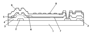
도 1은 ADS 모드에서의 종래 TFT 어레이 기판의 구조를 도시한다. 어레이 기판은 픽셀 영역을 정의하는 게이트 라인 및 데이터 라인을 포함하고, 픽셀 영역은 박막 트랜지스터 영역 및 전극 패턴 영역을 포함한다. 박막 트랜지스터 영역에는 게이트 전극(2), 게이트 절연층(3), 활성층(4), 소스 전극(5), 드레인 전극(6) 및 패시베이션층(9)을 형성한다. 전극 패턴 영역에는 게이트 절연층(3), 픽셀 전극(7), 패시베이션층(9) 및 공통 전극(8)을 형성한다. 공통 전극(8) 및 픽셀 전극(7)은 다차원 전계를 형성한다. 이 어레이 기판을 액정 디스플레이 장치에 적용하며, 액정 디스플레이 장치는 어레이 기판 이외에 컬러 필터 기판 및 백라이트 소스를 더 포함한다. 일반적으로, 어레이 기판 및 컬러 필터 기판이 별도로 제조하고, 그 후 셀 어셈블리 공정에 의해 접합시켜 디스플레이 패널을 형성하며, 최종적으로 모듈 공정에 의해 디스플레이 장치를 형성한다.1 shows the structure of a conventional TFT array substrate in ADS mode. The array substrate includes a gate line and a data line defining a pixel region, and the pixel region includes a thin film transistor region and an electrode pattern region. In the thin film transistor region, a
그러나 상이한 두께를 갖는 TFT 영역(도 1에 도시된 바와 같이, TFT에서 패시베이션층(9)은 분명한 돌출부를 가짐)은 셀 어셈블리 공정 후 액정 분자들의 충진 균일성(filling uniformity)에 영향을 미치므로, 반사 영역에는 액정 분자들의 불규칙 배열이 존재한다. 또한, 픽셀 전극은 비교적 데이터 라인에 가깝기 때문에, 데이터 라인의 전압으로부터 영향을 받을 수 있는데, 이는 ADS 모드의 수평 구동에 바람직하지 않다. 이 경우, 비정상 액정 구동으로 인해 액정 분자들의 회전각이 불충분할 수 있기 때문에 광누설이 발생할 수 있다. 광누설로 인해 백라이트 소스로부터의 광이 디스플레이 영역에서 충분히 이용되지 않을 수 있고, 이에 따라 콘트라스트가 감소하고, 디스플레이 품질이 저하될 수 있다.However, TFT regions having different thicknesses (as shown in FIG. 1, the
본 발명의 일 실시예에 따라, 어레이 기판이 제공된다. 어레이 기판은 픽셀 영역을 정의하는 게이트 라인 및 데이터 라인을 포함하며, 픽셀 영역은 박막 트랜지스터 영역 및 전극 패턴 영역을 포함하고, 박막 트랜지스터 영역에는 게이트 전극, 게이트 절연층, 활성층, 소스 전극, 드레인 전극 및 패시베이션층을 형성하고, 전극 패턴 영역에는 게이트 절연층, 픽셀 전극, 패시베이션층 및 공통 전극을 형성하며, 공통 전극 및 픽셀 전극은 다차원 전계를 형성한다. 게이트 절연층과 픽셀 전극 간에는 컬러 수지층을 형성한다.According to one embodiment of the invention, an array substrate is provided. The array substrate includes a gate line and a data line defining a pixel region, wherein the pixel region includes a thin film transistor region and an electrode pattern region, and the thin film transistor region includes a gate electrode, a gate insulating layer, an active layer, a source electrode, a drain electrode, and A passivation layer is formed, a gate insulating layer, a pixel electrode, a passivation layer, and a common electrode are formed in the electrode pattern region, and the common electrode and the pixel electrode form a multidimensional electric field. A color resin layer is formed between the gate insulating layer and the pixel electrode.
본 발명의 다른 실시예에 따라, 어레이 기판의 제조 방법이 제공된다. 이 방법은 픽셀 영역을 형성하는 단계를 포함하고, 픽셀 영역은 박막 트랜지스터 영역 및 전극 패턴 영역을 포함하고, 박막 트랜지스터 영역에는 게이트 전극, 게이트 절연층, 활성층, 소스 전극, 드레인 전극 및 패시베이션층을 형성하고, 전극 패턴 영역에는 게이트 절연층, 픽셀 전극, 패시베이션층 및 공통 전극을 형성하고, 공통 전극 및 픽셀 전극은 다차원 전계를 형성한다. 게이트 절연층 형성 후 픽셀 전극 형성 전에, 게이트 절연층 위에 컬러 수지층을 형성한다.According to another embodiment of the present invention, a method of manufacturing an array substrate is provided. The method includes forming a pixel region, the pixel region including a thin film transistor region and an electrode pattern region, wherein the thin film transistor region forms a gate electrode, a gate insulating layer, an active layer, a source electrode, a drain electrode, and a passivation layer. The gate insulating layer, the pixel electrode, the passivation layer, and the common electrode are formed in the electrode pattern region, and the common electrode and the pixel electrode form a multidimensional electric field. After forming the gate insulating layer and before forming the pixel electrode, a color resin layer is formed on the gate insulating layer.
본 발명의 다른 실시예에 따라, 디스플레이 장치가 제공된다. 디스플레이 장치는 전술된 어레이 기판을 포함한다.According to another embodiment of the present invention, a display device is provided. The display device includes the array substrate described above.
본 발명의 실시예에 따르면, 컬러 수지층을 게이트 절연층 위에 형성하여, 픽셀 전극과 데이터 라인 또는 게이트 라인 간의 거리가 증가하므로(즉, 층간 두께가 증가함), 픽셀 영역을 더욱 평평하게 하고 픽셀 전극이 데이터 라인 및 게이트 라인의 전압에 의해 영향받지 않도록 하는 것이 바람직하다. 따라서, 반사 영역 내의 액정 분자들의 불규칙한 배열을 방지할 수 있고, 수평 구동의 ADS 모드를 유지할 수 있고, 액정 분자들의 적절한 회전이 보장할 수 있고, 광누설을 방지할 수 있으며, 콘트라스트를 향상시킬 수 있다.According to an embodiment of the present invention, the color resin layer is formed over the gate insulating layer, so that the distance between the pixel electrode and the data line or the gate line is increased (that is, the interlayer thickness is increased), thereby making the pixel area more flat and the pixel It is desirable to ensure that the electrodes are not affected by the voltages of the data lines and gate lines. Therefore, irregular arrangement of liquid crystal molecules in the reflection area can be prevented, the ADS mode of horizontal driving can be maintained, proper rotation of the liquid crystal molecules can be ensured, light leakage can be prevented, and contrast can be improved. have.
본 발명의 실시예에 따르면, 반사 영역 패턴은 게이트 전극용 금속 재료를 이용하여 형성하고, 반사 영역 금속 전극층은 소스 및 드레인 전극들용 금속재료를 이용하여 형성하며, 컬러 수지층은 반사 영역 금속 전극층 상에 형성한다. 또한, 픽셀 전극과 반사 영역 전극층 간의 거리를 증가시켜, 반사 영역 내의 액정 분자들의 불규칙 배열에 기인한 광누설을 방지할 수 있는 것이 바람직하다. 또한, 반사 영역의 배치(즉, 반사투과형 방식 이용)를 통해 액정 디스플레이 장치는 외부 광(extern light)을 이용하여 강한 광 하에서 디스플레이 효과를 증대시킬 수 있으므로, 제품 품질을 향상시킬 수 있고 제조 비용을 절감할 수 있다.According to an embodiment of the present invention, the reflective region pattern is formed using the metal material for the gate electrode, the reflective region metal electrode layer is formed using the metal material for the source and drain electrodes, and the color resin layer is the reflective region metal electrode layer. Form on the phase. In addition, it is desirable to increase the distance between the pixel electrode and the reflective region electrode layer to prevent light leakage due to irregular arrangement of liquid crystal molecules in the reflective region. In addition, by arranging the reflective areas (ie, using a transmissive method), the liquid crystal display device can use an external light to increase the display effect under strong light, thereby improving product quality and manufacturing costs. Can be saved.
본 발명의 실시예들에 따르면, 어레이 기판을 별도의 컬러 필터 기판과 접합할 필요가 없으므로, 액정 분자들을 어레이 기판과 글라스 기판 사이에 충진하여, 배향의 곤란함을 감소시킬 수 있다. 한편, 공통 전극은 절연층 내의 비아홀을 통하여 저장 용량(storage capacitance)의 하부 전극에 접속하므로, 고개구율을 얻을 수 있고 투과율을 증가시킬 수 있다.According to embodiments of the present invention, since the array substrate does not need to be bonded to a separate color filter substrate, liquid crystal molecules may be filled between the array substrate and the glass substrate, thereby reducing difficulty of alignment. On the other hand, since the common electrode is connected to the lower electrode of the storage capacitance through the via hole in the insulating layer, a high opening ratio can be obtained and the transmittance can be increased.
본 발명의 실시예들의 기술적 해법들을 설명하기 위하여, 실시예들의 도면들에 대한 간단한 설명이 아래와 같이 주어진다. 아래 설명된 도면들은 본 발명의 일부 실시예들에 관한 것일 뿐이며, 본 발명을 한정하려는 것이 아님은 자명하다.
도 1은 ADS 모드에서 종래 어레이 기판을 도시하는 개략도.
도 2는 본 발명의 제1 실시예에 따른 어레이 기판을 도시하는 개략도.
도 3a 및 도 3b는 본 발명의 제1 실시예에 따른 어레이 기판 제조 방법을 도시하는 개략도.
도 4는 본 발명의 제2 실시예에 따른 어레이 기판을 도시하는 개략도.In order to explain the technical solutions of the embodiments of the present invention, a brief description of the drawings of the embodiments is given below. It is apparent that the drawings described below are only related to some embodiments of the present invention and are not intended to limit the present invention.
1 is a schematic diagram illustrating a conventional array substrate in ADS mode.
2 is a schematic diagram showing an array substrate according to a first embodiment of the present invention.
3A and 3B are schematic views showing an array substrate manufacturing method according to a first embodiment of the present invention.
4 is a schematic diagram illustrating an array substrate according to a second embodiment of the present invention.
본 발명의 목적, 기술적 해법 및 장점들이 더욱 명확해지도록 하기 위하여, 본 발명의 실시예들의 기술적 해법들은 본 발명의 실시예들의 도면들과 연계하여 충분히 명확하게 이하에서 설명될 것이다. 설명된 실시예들은 본 발명의 모든 실시예들이 아니라 그 중 일부임이 명확하다. 본 발명의 설명된 실시예들에 기초하여, 당업자가 창의적인 연구를 수행하지 않고 획득할 수 있는 모든 추가적인 실시예들은 본 발명의 보호범위에 포함된다.
BRIEF DESCRIPTION OF THE DRAWINGS In order that the objects, technical solutions and advantages of the present invention will become more apparent, the technical solutions of the embodiments of the present invention will be described below sufficiently clearly in connection with the drawings of the embodiments of the present invention. Apparently, the described embodiments are a part rather than all of the embodiments of the present invention. Based on the described embodiments of the present invention, all additional embodiments that can be obtained by a person skilled in the art without performing creative research are included in the protection scope of the present invention.
제1 실시예First Embodiment
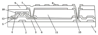
본 실시예는 ADS 모드를 이용할 수 있는 어레이 기판을 제공한다. 도 2에 도시된 바와 같이, 어레이 기판은 픽셀 영역을 정의하는 게이트 라인 및 데이터 라인을 포함하고, 픽셀 영역은 박막 트랜지스터 영역 및 전극 패턴 영역을 포함한다. 박막 트랜지스터 영역에는 게이트 전극(2), 게이트 절연층(3), 활성층(4), 소스 전극(5), 드레인 전극(6), 및 패시베이션층(9)을 형성한다. 전극 패턴 영역에는 게이트 절연층(3), 픽셀 전극(7), 패시베이션층(9) 및 공통 전극(8)을 형성한다. 공통 전극(8) 및 픽셀 전극(7)은 다차원 전계를 형성할 수 있다. 이와 달리, 보호층(12)을 게이트 절연층(3), 소스 전극(5) 및 드레인 전극(6) 상에 형성할 수 있으며, 후속하여 블랙 매트릭스층(10)을 소스 전극(5), 드레인 전극(6) 및 TFT 채널 위에 형성할 수 있다. 이와 달리, 보호층(12)을 형성하지 않고 소스 전극(5), 드레인 전극(6) 및 TFT 채널 위에 블랙 매트릭스층(10)을 직접 형성할 수 있다.This embodiment provides an array substrate that can utilize the ADS mode. As shown in FIG. 2, the array substrate includes a gate line and a data line defining a pixel region, and the pixel region includes a thin film transistor region and an electrode pattern region. In the thin film transistor region, a
보호층(12)을 형성하는 경우, 박막 트랜지스터에 대응하는 보호층(12) 부분 상에 블랙 매트릭스층(10)을 형성되고, 보호층(12)과 블랙 매트릭스층(10)에 의해 형성되는 표면과 픽셀 전극(7) 간에 컬러 수지층(color resin layer, 11)을 형성한다. 보호층(12)을 형성하지 않고 박막 트랜지스터 상에 블랙 매트릭스층(10)을 직접 형성하는 경우, 게이트 절연층(3)과 블랙 매트릭스층(10)에 의해 형성되는 표면과 픽셀 전극(7) 간에 컬러 수지층(11)을 형성한다. 픽셀 영역을 더욱 평평하게 하는 데에는 보호층(12)이 바람직하다.In the case of forming the
전극 패턴 영역에는 게이트 전극(2)용 금속 재료로 형성한 저장 용량 하부 전극(13)을 더 구비한다. 저장 용량 하부 전극(13) 위에는 절연층 비아홀(insulation layer via hole)을 형성한다. 절연층 비아홀은 패시베이션층(9), 컬러 수지층(11), 보호층(12)(형성되는 경우) 및 게이트 절연층(3)을 통과한다. 공통 전극(8)은 절연층 비아홀을 통해 저장 용량 하부 전극(13)과 접속한다.The electrode pattern region is further provided with a storage capacitor
본 실시예에서, 저장 용량 하부 전극(13)은 공통 전극(8)에 일정 전압을 제공하는 공통 전극 라인(Cst on Common)이거나, 게이트 라인의 일부(Cst on Gate)일 수 있다.In the present embodiment, the storage capacitor
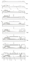
또한, 본 실시예는 어레이 기판의 제조 방법을 더 제공한다. 도 3a 및 3b에 도시된 바와 같이, 이 방법은 먼저 게이트 라인, 게이트 전극(2), 게이트 절연층(3), 활성층(4), 소스 전극(5), 드레인 전극(6) 및 데이터 라인을 형성하여 박막 트랜지스터 영역을 형성하고, 후속하여 컬러 수지층(11)을 형성하며, 최종적으로 픽셀 전극(7), 패시베이션층(9) 및 공통 전극(8)을 형성하여 전극 패턴 영역을 형성하는 단계를 포함한다. 예를 들어, 이 방법은 다음의 단계들을 포함한다:In addition, the present embodiment further provides a method of manufacturing the array substrate. As shown in Figs. 3A and 3B, the method first starts a gate line, a
단계 S1: 먼저 게이트 라인, 게이트 전극(2), 게이트 절연층(3), 활성층(4), 소스 전극(5), 드레인 전극(6) 및 데이터 라인을 형성하여 박막 트랜지스터 영역을 형성하고, 후속하여 절연재료에 의해 보호층(12)을 형성하는 단계. 이 단계는 다음의 단계들 S101, S102 및 S103을 포함할 수 있다:Step S1: First, a gate line, a
단계 S101: 기판(1) 상에 도전성을 갖는 제1 금속층을 피착하고, 제1 패터닝 공정을 이용하여 전극 패턴 영역에 게이트 라인, 게이트 전극(2), 및 저장 용량 하부 전극(13)을 형성하는 단계;Step S101: depositing a conductive first metal layer on the
단계 S102: 단계 S101 이후, 기판 상에 SiNx, SiON 등의 재료에 의해 형성된 게이트 절연층(3) 및 a-Si 등의 재료에 의해 형성된 반도체 활성층(4)을 순차적으로 피착하고, 도전성을 갖는 제2 금속층을 피착하며, 하프톤 마스크 또는 그레이톤 마스크를 이용하여 제2 패터닝 공정을 통해 활성층(4), 소스 전극(5), 드레인 전극(6) 및 데이터 라인을 형성하여 박막 트랜지스터 영역을 형성하는 단계,Step S102: After step S101, a
단계 S103: 단계 S102 이후, 기판 상에 SiNx 등의 재료를 이용하여 보호층(12)을 형성하여 픽셀 영역을 보호하는 단계 - .Step S103: after step S102, protecting the pixel region by forming a
단계 S2: 단계 S1 이후, 기판 상에 불투명 수지층을 피착하고, 제3 패터닝 공정을 이용하여 박막 트랜지스터 영역의 소정 위치에 블랙 매트릭스층(10)을 형성하는 단계.Step S2: After Step S1, depositing an opaque resin layer on the substrate and forming a
단계 S3: 컬러 수지층(11)을 형성하는 단계. 이 단계는 다음의 단계들 S301 및 S302를 포함한다: Step S3: forming the
단계 S301: 단계 S2 이후, 기판 상에 적색 수지층 R을 피착하고 제4 패터닝 공정을 수행하고, 적색 수지층 R과 유사한 방식으로 녹색 수지층 G 및 청색 수지층 B를 피착하고 제5 패터닝 공정 및 제6 패터닝 공정을 수행하여 컬러 수지층(11)을 형성하며, 저장 용량 하부 전극(13) 위의 컬러 수지층(11)을 에칭 제거(etching away)하는 단계;Step S301: After Step S2, a red resin layer R is deposited on the substrate and a fourth patterning process is performed, and the green resin layer G and the blue resin layer B are deposited in a similar manner to the red resin layer R, and the fifth patterning process and Performing a sixth patterning process to form the
단계 S302: 제7 패터닝 공정을 이용하여 저장 용량 하부 전극(13) 위의 게이트 절연층(3) 및 보호층(12)을 에칭 제거하여, 저장 용량 하부 전극(13)을 노출하고 위쪽으로 개방된 절연층 비아홀을 형성하는 단계 - .Step S302: The
다음의 단계들 S4 및 S5에서, 픽셀 전극(7), 패시베이션층(9) 및 공통 전극(8)을 형성할 것이다. 예를 들어, 이 단계들은 다음과 같이 수행된다:In the following steps S4 and S5, the
단계 S4: 단계 S3 이후, 기판 상에 제1 투명 도전층을 피착하고 제8 패터닝 공정을 이용하여 픽셀 전극(7)을 형성하는 단계;Step S4: after step S3, depositing a first transparent conductive layer on the substrate and forming a
단계 S5: 패시베이션층(9) 및 공통 전극(8)을 형성하는 단계. 공통 전극(8)은 단계 S302에서 형성된 절연층 비아홀을 통해 저장 용량 하부 전극(13)과 접속한다. 이 단계는 다음의 단계들 S501 및 S502를 포함한다:Step S5: forming the
단계 S501: 단계 S4 이후, 기판 상에 투명 레진 재료층을 피착하고, 제9 패터닝 공정을 이용하여 패시베이션층(9)을 형성하는 단계;Step S501: after step S4, depositing a transparent resin material layer on the substrate and forming a
단계 S502: 단계 S501 이후, 기판 상에 제2 투명 도전층을 피착하고, 제10 패터닝 공정을 이용하여 공통 전극(8)을 형성하는 단계.Step S502: After step S501, depositing a second transparent conductive layer on the substrate and forming a
전술된 제조 방법에서, 불투명 수지층을 형성하기 위한 재료는 1012 Ω/sq 보다 큰 시트저항, 0.5 ㎛ 내지 2 ㎛의 두께, 및 4 보다 큰 광학밀도(OP:optical density)를 갖는 것이 바람직하다.In the above-described manufacturing method, the material for forming the opaque resin layer preferably has a sheet resistance of greater than 10 12 Ω / sq, a thickness of 0.5 µm to 2 µm, and an optical density (OP) of greater than 4. .
바람직하게는, R, G 및 B 수지층들을 형성하기 위한 재료는 3 내지 5 F/m 범위의 유전율 및 1 ㎛ 내지 4 ㎛의 두께를 갖는 것이 좋다.Preferably, the material for forming the R, G, and B resin layers preferably has a dielectric constant in the range of 3 to 5 F / m and a thickness of 1 to 4 μm.
제1 및 제2 투명 도전층들을 형성하기 위한 재료는 바람직하게는 배선 금속(예를 들어, Mo, Al, Ti, Cu 등과 같이 도전성을 갖는 금속 또는 합금)에 대하여 습식에칭 선택성을 가지는 것으로서, 예를 들어 ITO(indium tin oxide), IZO(indium zinc oxide) 등이다. 이 재료는 TCO(Transparent Conducting Oxide)의 처리 후 양호한 투명성을 갖는다.The material for forming the first and second transparent conductive layers is preferably one having wet etching selectivity with respect to the wiring metal (eg, a conductive metal or alloy such as Mo, Al, Ti, Cu, etc.), for example For example, ITO (indium tin oxide), IZO (indium zinc oxide). This material has good transparency after the treatment of Transparent Conducting Oxide (TCO).
바람직하게는, 패시베이션층(9)을 형성하기 위한 투명 레진 재료층은 3 내지 5 F/m 범위의 유전율 및 1 ㎛ 내지 4 ㎛의 두께를 갖는다.Preferably, the transparent resin material layer for forming the
블랙 매트릭스층, R, G 및 B 수지층들을 형성하기 위한 상기 불투명 수지층 및 패시베이션층을 형성하기 위한 투명 레진 재료층은 모재(matrix)로서 아크릴레이트, 폴리이미드, 에폭시 레진, 페놀알데히드 레진 등을 이용할 수 있다. 불투명 수지층 및 R, G, 및 B 수지층들은 모재에 상이한 컬러의 색소 또는 염료를 첨가하여 형성된다.
The transparent resin material layer for forming the opaque resin layer and the passivation layer for forming the black matrix layer, the R, G, and B resin layers is formed of acrylate, polyimide, epoxy resin, phenolaldehyde resin, or the like as a matrix. It is available. The opaque resin layer and the R, G, and B resin layers are formed by adding dyes or dyes of different colors to the base material.
제2 실시예Second Embodiment
본 실시예는 다른 어레이 기판을 제공한다. 본 실시예에서는 상기 제1 실시예의 반복되는 설명은 생략될 것이고, 본 실시예와 제1 실시예 간의 차이점들을 아래에 상세히 설명할 것이다.This embodiment provides another array substrate. In this embodiment, repeated description of the first embodiment will be omitted, and differences between the present embodiment and the first embodiment will be described in detail below.
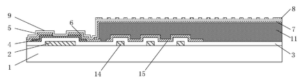
본 실시예에 의해 제공되는 어레이 기판은 ADS 모드를 이용할 수 있다. 도 4에 도시된 바와 같이, 어레이 기판은 픽셀 영역을 정의하는 게이트 라인 및 데이터 라인을 포함하고, 픽셀 영역은 박막 트랜지스터 영역 및 전극 패턴 영역을 포함한다. 박막 트랜지스터 영역에는 게이트 전극(2), 게이트 절연층(3), 활성층(4), 소스 전극(5), 드레인 전극(6), 및 패시베이션층(9)을 형성한다. 전극 패턴 영역에는 게이트 절연층(3), 픽셀 전극(7), 패시베이션층(9) 및 공통 전극(8)을 형성한다. 공통 전극(8) 및 픽셀 전극(7)은 다차원 전계를 형성할 수 있다.The array substrate provided by this embodiment may use ADS mode. As shown in FIG. 4, the array substrate includes a gate line and a data line defining a pixel region, and the pixel region includes a thin film transistor region and an electrode pattern region. In the thin film transistor region, a
게이트 전극(2)용 금속 재료로 형성된 반사 영역 패턴(14)은 기판(1) 상의 전극 패턴 영역에 대응하는 위치에 배치한다. 게이트 절연층(3)은 반사 영역 패턴(14) 상에 형성한다. 소스 및 드레인 전극들용 금속 재료로 형성하는 반사 영역 금속 전극층(15)은 게이트 절연층(3) 상의 반사 영역 패턴(14)에 대응하는 위치에 배치한다. 따라서, 옥외와 같은 강한 광의 환경에서 이용할 수 있는 반사투과형 어레이 기판을 형성한다.The
또한, 본 실시예는 어레이 기판 제조 방법을 제공한다. 이 방법은 다음의 단계들을 포함한다:In addition, the present embodiment provides an array substrate manufacturing method. The method includes the following steps:
단계 1: 제1 금속 재료를 이용하여 게이트 라인, 게이트 전극(2) 및 저장 용량 하부 전극(도시하지 않음)을 형성하고, 전극 패턴 영역 내의 소정 위치들에서 제1 금속재료 부분을 남겨두고, 제1 금속 재료를 이용하여 요철 패턴을 형성함으로서 반사 영역 패턴(14)을 형성하는 단계 - 제1 금속 재료는 바람직하게는 Al, AlNd, Mo 등임 - .Step 1: forming the gate line, the
본 실시예에서, 저장 용량 하부 전극은 공통 전극에 일정 전압을 제공하는 공통 전극 라인(Cst on Common)이거나, 게이트 라인의 일부(Cst on Gate)일 수 있다.In the present exemplary embodiment, the storage capacitor lower electrode may be a common electrode line Cst on Common that provides a constant voltage to the common electrode, or a portion of the gate line Cst on Gate.
단계 2: 게이트 절연층(3)을 형성하고, 반도체 재료를 이용하여 반도체 아일랜드를 형성하여 활성층(4)을 형성하는 단계 - 반도체 재료는 바람직하게는 a-Si, p-Si, IGZO 등임 - .Step 2: forming a
단계 3: 제2 금속 재료를 이용하여 데이터 라인, 소스 전극(5) 및 드레인 전극(6)을 형성하고, 반사 영역 패턴(14)에 대응하는 게이트 절연층(3) 상의 제2 금속 재료 부분을 남겨두어, 반사층의 기능을 달성하기 위해 이용되는 반사 영역 금속 전극층(15)을 형성하는 단계 - 제2 금속 재료는 바람직하게는 Al, AlNd, Mo 등임 - .Step 3: Form the data line, the
단계 4 내지 6: 적색 수지층 R을 피착하고 패터닝 공정을 수행하며, 적색 수지층과 유사한 방식으로 녹색 수지층 G 및 청색 수지층 B를 피착하고 패터닝 공정을 수행하여, 컬러 수지층(11)을 형성하는 단계.
단계 7: 투명 도전 재료를 이용하여 드레인 전극(6)과 접속하는 픽셀 전극(7)을 형성하는 단계 - 투명 도전 재료는 바람직하게는 ITO, IZO 등임 - .Step 7: forming the
단계 8: 무기 절연 재료를 이용하여 패시베이션층(9)을 형성하는 단계 - 무기 절연 재료는 바람직하게는 SiNx, SiOx 등임 - .Step 8: forming the
단계 9: 투명 도전 재료를 이용하여 공통 전극(8)을 형성하는 단계 - 공통 전극(8)은 비아홀(도시하지 않음)에 의해 저장 용량 하부 전극과 접속하고, 투명 도전 재료는 바람직하게는 ITO, IZO 등임 - .Step 9: forming the
또한, 불투명 수지층을 이용하여 얻어지는 어레이 기판 상의 박막 트랜지스터 영역 상에 블랙 매트릭스층을 순차적으로 형성할 수 있다.Further, the black matrix layer can be sequentially formed on the thin film transistor region on the array substrate obtained by using the opaque resin layer.
픽셀 전극은 판형 또는 슬릿형일 수 있고, 그에 따라, 공통 전극은 슬릿형 또는 판형일 수 있는 것을 당업자는 이해할 수 있다. 픽셀 전극과 공통 전극의 적층 순서는 반대로 할 수 있지만, 상부 전극은 슬릿형이어야 하고 하부 전극은 판형이어야 한다.Those skilled in the art will appreciate that the pixel electrode may be plate-like or slit-like, and thus the common electrode may be slit-like or plate-like. The stacking order of the pixel electrode and the common electrode may be reversed, but the upper electrode should be slit type and the lower electrode should be plate type.
본 발명의 실시예들은 또한, 상기 실시예들에 따른 어레이 기판을 포함하는 디스플레이 장치를 제공한다. 디스플레이 장치는 액정 패널, 전자 종이, OLED 패널, 액정 TV, 액정 디스플레이, 디지털 포토 프레임, 휴대 전화, 평판 컴퓨터 등과 같이 디스플레이 기능을 갖는 임의의 제품들 또는 컴포넌트들일 수 있다.Embodiments of the present invention also provide a display device including the array substrate according to the embodiments. The display device may be any products or components having a display function, such as a liquid crystal panel, an electronic paper, an OLED panel, a liquid crystal TV, a liquid crystal display, a digital photo frame, a mobile phone, a flat panel computer, and the like.
상기 설명은 단지 본 발명의 바람직한 실시예들이다. 당업자는 본 발명의 기술적 원리를 벗어나지 않고 다양한 변형 및 수정을 가능하며, 이 변형들 및 수정들은 본 발명의 보호범위 내에 있는 것으로 판단되어야 한다.The above description is merely preferred embodiments of the present invention. Those skilled in the art can make various changes and modifications without departing from the technical principles of the present invention, which should be determined to be within the protection scope of the present invention.
Claims (9)
상기 픽셀 영역은 박막 트랜지스터 영역 및 전극 패턴 영역을 포함하고,
상기 박막 트랜지스터 영역에는 게이트 전극, 게이트 절연층, 활성층, 소스 전극, 드레인 전극 및 패시베이션층을 형성하고,
상기 전극 패턴 영역에는 상기 게이트 절연층, 픽셀 전극, 상기 패시베이션층 및 공통 전극을 형성하고,
상기 공통 전극 및 상기 픽셀 전극은 다차원 전계를 형성하도록 이용하며,
상기 게이트 절연층과 상기 픽셀 전극 간에는 컬러 수지층을 형성하는
어레이 기판.An array substrate comprising a gate line and a data line defining a pixel region, the array substrate comprising:
The pixel region includes a thin film transistor region and an electrode pattern region,
A gate electrode, a gate insulating layer, an active layer, a source electrode, a drain electrode, and a passivation layer are formed in the thin film transistor region,
Forming the gate insulating layer, the pixel electrode, the passivation layer, and the common electrode in the electrode pattern region;
The common electrode and the pixel electrode are used to form a multidimensional electric field,
A color resin layer is formed between the gate insulating layer and the pixel electrode.
Array substrate.
상기 기판 상의 상기 전극 패턴 영역에 대응하는 위치에 상기 게이트 전극용 금속 재료로 형성되는 반사 영역 패턴을 배치하고, 상기 게이트 절연층은 상기 반사 영역 패턴 상에 형성하며,
상기 게이트 절연층 상의 상기 반사 영역 패턴에 대응하는 위치에 상기 소스 및 드레인 전극들용 금속 재료로 형성되는 반사 영역 금속 전극층을 배치하는
어레이 기판.The method of claim 1,
A reflective region pattern formed of the gate electrode metal material is disposed at a position corresponding to the electrode pattern region on the substrate, and the gate insulating layer is formed on the reflective region pattern,
A reflective region metal electrode layer formed of a metal material for the source and drain electrodes is disposed at a position corresponding to the reflective region pattern on the gate insulating layer.
Array substrate.
어레이 기판.The storage electrode of claim 1, wherein a storage capacitor lower electrode formed of the gate electrode metal material is disposed in the electrode pattern region, an insulating layer via hole is formed on the storage capacitor lower electrode, and the common electrode is formed by the insulating layer via hole. Is connected to the storage capacitor lower electrode
Array substrate.
어레이 기판.The method of claim 1, further comprising: forming a protective layer formed of an insulating material on the source electrode, the drain electrode, and the gate insulating layer, and forming a black matrix layer at a position corresponding to the thin film transistor region on the protective layer.
Array substrate.
상기 픽셀 영역은 박막 트랜지스터 영역 및 전극 패턴 영역을 포함하고,
상기 박막 트랜지스터 영역에는 게이트 전극, 게이트 절연층, 활성층, 소스 전극, 드레인 전극 및 패시베이션층을 형성하고,
상기 전극 패턴 영역에는 상기 게이트 절연층, 픽셀 전극, 상기 패시베이션층 및 공통 전극을 형성하고, 상기 공통 전극 및 상기 픽셀 전극은 다차원 전계를 형성하도록 이용하며,
상기 게이트 절연층을 형성한 후 상기 픽셀 전극을 형성하기 전에, 상기 게이트 절연층 위에 컬러 수지층을 형성하는
어레이 기판 제조 방법.An array substrate manufacturing method comprising forming a pixel region, the method comprising:
The pixel region includes a thin film transistor region and an electrode pattern region,
A gate electrode, a gate insulating layer, an active layer, a source electrode, a drain electrode, and a passivation layer are formed in the thin film transistor region,
The gate insulating layer, the pixel electrode, the passivation layer, and the common electrode are formed in the electrode pattern region, and the common electrode and the pixel electrode are used to form a multi-dimensional electric field.
After forming the gate insulating layer and before forming the pixel electrode, a color resin layer is formed on the gate insulating layer.
Array substrate manufacturing method.
상기 게이트 전극 형성시, 상기 기판 상의 상기 전극 패턴 영역과 대응하는 위치에 상기 게이트 전극용 금속 재료로 형성되는 반사 영역 패턴을 배치하고,
상기 소스 및 드레인 전극들의 형성시, 상기 게이트 절연층 상의 상기 반사 영역 패턴에 대응하는 위치에 상기 소스 및 드레인 전극들용 금속 재료로 형성되는 반사 영역 금속 전극층을 배치하는
어레이 기판 제조 방법.The method of claim 5,
When forming the gate electrode, a reflective region pattern formed of the metal material for the gate electrode is disposed at a position corresponding to the electrode pattern region on the substrate,
In forming the source and drain electrodes, a reflective region metal electrode layer formed of a metal material for the source and drain electrodes is disposed at a position corresponding to the reflective region pattern on the gate insulating layer.
Array substrate manufacturing method.
상기 게이트 전극 형성시, 상기 전극 패턴 영역에 상기 게이트 전극용 금속 재료로 형성되는 저장 용량 하부 전극을 배치하고,
상기 공통 전극을 형성하기 전에 상기 저장 용량 하부 전극 위에 절연층 비아홀을 형성하여, 상기 공통 전극은 상기 절연층 비아홀을 통해 상기 저장 용량 하부 전극과 접속하는
어레이 기판 제조 방법.The method of claim 5,
When the gate electrode is formed, a storage capacitor lower electrode formed of the gate electrode metal material is disposed in the electrode pattern region,
Before forming the common electrode, an insulating layer via hole is formed on the storage capacitor lower electrode so that the common electrode is connected to the storage capacitor lower electrode through the insulating layer via hole.
Array substrate manufacturing method.
어레이 기판 제조 방법.The method of claim 5, wherein after forming the source and drain electrodes, a protective layer formed of an insulating material is formed, and a black matrix layer is formed at a position corresponding to the thin film transistor region on the protective layer.
Array substrate manufacturing method.
Applications Claiming Priority (3)
| Application Number | Priority Date | Filing Date | Title |
|---|---|---|---|
| CN201210048847.8 | 2012-02-28 | ||
| CN201210048847.8A CN102681276B (en) | 2012-02-28 | 2012-02-28 | Array substrate, method for manufacturing same and display device comprising same |
| PCT/CN2012/087234 WO2013127236A1 (en) | 2012-02-28 | 2012-12-23 | Array substrate, manufacturing method therefor and display device |
Publications (1)
| Publication Number | Publication Date |
|---|---|
| KR20130108574A true KR20130108574A (en) | 2013-10-04 |
Family
ID=46813420
Family Applications (1)
| Application Number | Title | Priority Date | Filing Date |
|---|---|---|---|
| KR1020137008359A KR20130108574A (en) | 2012-02-28 | 2012-12-23 | Array substrate, manufacturing method thereof, and display device |
Country Status (6)
| Country | Link |
|---|---|
| US (1) | US20140054581A1 (en) |
| EP (1) | EP2660651B1 (en) |
| JP (1) | JP2015511026A (en) |
| KR (1) | KR20130108574A (en) |
| CN (1) | CN102681276B (en) |
| WO (1) | WO2013127236A1 (en) |
Cited By (1)
| Publication number | Priority date | Publication date | Assignee | Title |
|---|---|---|---|---|
| KR20170086660A (en) * | 2014-12-19 | 2017-07-26 | 센젠 차이나 스타 옵토일렉트로닉스 테크놀로지 컴퍼니 리미티드 | Ffs array substrate and liquid crystal display panel |
Families Citing this family (46)
| Publication number | Priority date | Publication date | Assignee | Title |
|---|---|---|---|---|
| CN202404339U (en) * | 2012-01-12 | 2012-08-29 | 京东方科技集团股份有限公司 | Array substrate and display device comprising same |
| CN102681276B (en) * | 2012-02-28 | 2014-07-09 | 京东方科技集团股份有限公司 | Array substrate, method for manufacturing same and display device comprising same |
| TWI547477B (en) | 2012-03-14 | 2016-09-01 | 大賽璐股份有限公司 | Process for producing acetic acid |
| CN102854685A (en) * | 2012-09-26 | 2013-01-02 | 南京中电熊猫液晶显示科技有限公司 | Metallic oxide fringing field switching mode liquid crystal display panel and manufacture method thereof |
| CN102931139B (en) * | 2012-11-05 | 2015-07-01 | 京东方科技集团股份有限公司 | Array substrate and manufacture method and display device thereof |
| CN102998867B (en) * | 2012-11-20 | 2015-06-03 | 京东方科技集团股份有限公司 | Array substrate, display panel, manufacturing method and display device |
| CN103018991B (en) * | 2012-12-24 | 2015-01-28 | 京东方科技集团股份有限公司 | Array substrate, manufacturing method thereof and display device |
| CN103117284A (en) * | 2013-02-01 | 2013-05-22 | 京东方科技集团股份有限公司 | Array substrate and manufacturing method thereof and display device |
| CN103309095B (en) * | 2013-05-30 | 2015-08-26 | 京东方科技集团股份有限公司 | A kind of array base palte and preparation method thereof, display device |
| CN103309081B (en) * | 2013-05-30 | 2016-12-28 | 京东方科技集团股份有限公司 | Array base palte and manufacture method, display device |
| CN103309106B (en) * | 2013-07-10 | 2015-11-11 | 深圳市华星光电技术有限公司 | Colorful filter array substrate and manufacture method thereof |
| JP6188473B2 (en) * | 2013-07-31 | 2017-08-30 | 三菱電機株式会社 | Thin film transistor array substrate and manufacturing method thereof |
| CN103487982A (en) * | 2013-08-19 | 2014-01-01 | 京东方科技集团股份有限公司 | Display device, array substrate, pixel structure and manufacturing method |
| CN103472646B (en) * | 2013-08-30 | 2016-08-31 | 京东方科技集团股份有限公司 | A kind of array base palte and preparation method thereof and display device |
| CN103456764B (en) * | 2013-09-09 | 2016-01-20 | 京东方科技集团股份有限公司 | OLED array and manufacture method, display unit |
| CN103489826B (en) | 2013-09-26 | 2015-08-05 | 京东方科技集团股份有限公司 | Array base palte, preparation method and display unit |
| TWI642170B (en) * | 2013-10-18 | 2018-11-21 | 半導體能源研究所股份有限公司 | Display device and electronic device |
| CN103700669A (en) * | 2013-12-19 | 2014-04-02 | 京东方科技集团股份有限公司 | Array substrate and preparation method thereof as well as display device |
| CN103715204B (en) * | 2013-12-27 | 2015-05-27 | 京东方科技集团股份有限公司 | Array substrate, manufacturing method thereof and display device |
| CN103928472A (en) * | 2014-03-26 | 2014-07-16 | 京东方科技集团股份有限公司 | Array substrate, manufacturing method of array substrate and display device |
| CN104090434B (en) * | 2014-06-25 | 2016-10-05 | 京东方科技集团股份有限公司 | Array base palte and display device |
| CN104216186B (en) * | 2014-08-15 | 2018-01-26 | 京东方科技集团股份有限公司 | Array base palte and its manufacture method, display device |
| CN104332473A (en) * | 2014-08-29 | 2015-02-04 | 京东方科技集团股份有限公司 | Array substrate and preparation method thereof, display panel and display device |
| CN104298040B (en) * | 2014-10-31 | 2018-07-06 | 京东方科技集团股份有限公司 | A kind of COA substrates and preparation method thereof and display device |
| CN104317097A (en) * | 2014-10-31 | 2015-01-28 | 京东方科技集团股份有限公司 | COA (color filter on array) substrate, production method thereof and display device |
| CN104375344B (en) * | 2014-11-21 | 2017-09-15 | 深圳市华星光电技术有限公司 | Liquid crystal display panel and its color membrane array substrate |
| CN104536194A (en) * | 2015-01-04 | 2015-04-22 | 京东方科技集团股份有限公司 | Array substrate, method for manufacturing array substrate and display device |
| TWI557488B (en) | 2015-01-12 | 2016-11-11 | 群創光電股份有限公司 | Display |
| CN105842929B (en) * | 2015-01-12 | 2020-12-29 | 群创光电股份有限公司 | Display device |
| CN104617039A (en) * | 2015-01-27 | 2015-05-13 | 京东方科技集团股份有限公司 | Array substrate, and manufacture method and display device thereof |
| CN104617109B (en) * | 2015-01-28 | 2018-04-20 | 昆山龙腾光电有限公司 | Thin-film transistor array base-plate and preparation method thereof, liquid crystal display device |
| CN105990231B (en) * | 2015-02-25 | 2019-10-18 | 南京瀚宇彩欣科技有限责任公司 | The manufacturing method of thin film transistor base |
| CN104733456B (en) * | 2015-03-23 | 2018-04-27 | 京东方科技集团股份有限公司 | A kind of array base palte and preparation method thereof, display device |
| CN104765191B (en) | 2015-04-30 | 2018-07-06 | 京东方科技集团股份有限公司 | Array substrate and preparation method thereof and display device |
| CN104808408B (en) * | 2015-05-15 | 2018-09-07 | 合肥鑫晟光电科技有限公司 | A kind of production method of COA substrates, display device and COA substrates |
| CN104880847B (en) * | 2015-06-18 | 2019-04-30 | 深圳市华星光电技术有限公司 | IPS type On Cell touch-control display panel and preparation method thereof |
| CN104934449B (en) * | 2015-07-16 | 2017-12-05 | 京东方科技集团股份有限公司 | Display base plate and preparation method thereof and display device |
| KR102148491B1 (en) * | 2015-12-14 | 2020-08-26 | 엘지디스플레이 주식회사 | Thin film transistor substrate |
| JP6651859B2 (en) * | 2016-01-12 | 2020-02-19 | 凸版印刷株式会社 | Thin film transistor array and reflective display device |
| CN105511177A (en) | 2016-02-02 | 2016-04-20 | 京东方科技集团股份有限公司 | Array substrate and liquid crystal display device |
| CN106024810A (en) * | 2016-07-13 | 2016-10-12 | 京东方科技集团股份有限公司 | Flexible display substrate and manufacturing method thereof and display device |
| CN111446260B (en) * | 2020-03-31 | 2023-07-21 | 京东方科技集团股份有限公司 | Array substrate, preparation method thereof and display device |
| CN111694464B (en) * | 2020-06-19 | 2024-04-19 | 京东方科技集团股份有限公司 | Array substrate, preparation method thereof and display device |
| US11650705B2 (en) * | 2020-12-07 | 2023-05-16 | Tpk Advanced Solutions Inc. | Touch panel, electronic device and manufacture method thereof |
| JP2022139554A (en) * | 2021-03-12 | 2022-09-26 | セイコーエプソン株式会社 | Electro-optical device and electronic apparatus |
| CN114089570B (en) * | 2021-11-22 | 2023-11-10 | 京东方科技集团股份有限公司 | Array substrate, preparation method thereof, display panel and display device |
Family Cites Families (18)
| Publication number | Priority date | Publication date | Assignee | Title |
|---|---|---|---|---|
| JP2001066617A (en) * | 1999-08-27 | 2001-03-16 | Nec Corp | Liquid crystal display device and its production |
| TW575775B (en) * | 2001-01-29 | 2004-02-11 | Hitachi Ltd | Liquid crystal display device |
| JP3750055B2 (en) * | 2001-02-28 | 2006-03-01 | 株式会社日立製作所 | Liquid crystal display |
| KR100945442B1 (en) * | 2003-02-28 | 2010-03-05 | 엘지디스플레이 주식회사 | Color Filter on Transister Structrure Transflective Type Liquid Crystal Display Device |
| TWI261716B (en) * | 2004-05-13 | 2006-09-11 | Quanta Display Inc | Liquid crystal display apparatus and fabrication thereof |
| EP3229066A1 (en) * | 2005-12-05 | 2017-10-11 | Semiconductor Energy Laboratory Co., Ltd. | Transflective liquid crystal display with a horizontal electric field configuration |
| JP2007178810A (en) * | 2005-12-28 | 2007-07-12 | Lg Philips Lcd Co Ltd | Liquid crystal display device |
| TWI585498B (en) * | 2006-05-16 | 2017-06-01 | 半導體能源研究所股份有限公司 | Liquid crystal display device and semiconductor device |
| CN101495910B (en) * | 2006-08-02 | 2012-06-20 | 夏普株式会社 | Display device |
| JP4487318B2 (en) * | 2007-07-26 | 2010-06-23 | エプソンイメージングデバイス株式会社 | Liquid crystal display device and manufacturing method thereof |
| JP2009139853A (en) * | 2007-12-10 | 2009-06-25 | Sharp Corp | Liquid crystal display device |
| KR101423113B1 (en) * | 2007-12-18 | 2014-07-25 | 삼성디스플레이 주식회사 | Thin film transistor display substrate and method of faricating the same |
| US20110227817A1 (en) * | 2008-11-28 | 2011-09-22 | Katsunori Misaki | Liquid crystal display device and method for manufacturing liquid crystal display device tft substrate |
| TWI613489B (en) * | 2008-12-03 | 2018-02-01 | 半導體能源研究所股份有限公司 | Liquid crystal display device |
| KR101330330B1 (en) * | 2008-12-30 | 2013-11-15 | 엘지디스플레이 주식회사 | In-Plane Switching mode Liquid crystal display device |
| CN101968590B (en) * | 2010-10-27 | 2014-07-02 | 友达光电股份有限公司 | Liquid crystal display panel |
| CN202084547U (en) * | 2011-06-02 | 2011-12-21 | 北京京东方光电科技有限公司 | Array substrate, liquid crystal plane and display equipment |
| CN102681276B (en) * | 2012-02-28 | 2014-07-09 | 京东方科技集团股份有限公司 | Array substrate, method for manufacturing same and display device comprising same |
-
2012
- 2012-02-28 CN CN201210048847.8A patent/CN102681276B/en active Active
- 2012-12-23 EP EP12837626.6A patent/EP2660651B1/en active Active
- 2012-12-23 JP JP2014557978A patent/JP2015511026A/en active Pending
- 2012-12-23 KR KR1020137008359A patent/KR20130108574A/en active Search and Examination
- 2012-12-23 WO PCT/CN2012/087234 patent/WO2013127236A1/en active Application Filing
- 2012-12-23 US US13/878,475 patent/US20140054581A1/en not_active Abandoned
Cited By (1)
| Publication number | Priority date | Publication date | Assignee | Title |
|---|---|---|---|---|
| KR20170086660A (en) * | 2014-12-19 | 2017-07-26 | 센젠 차이나 스타 옵토일렉트로닉스 테크놀로지 컴퍼니 리미티드 | Ffs array substrate and liquid crystal display panel |
Also Published As
| Publication number | Publication date |
|---|---|
| EP2660651A1 (en) | 2013-11-06 |
| CN102681276B (en) | 2014-07-09 |
| JP2015511026A (en) | 2015-04-13 |
| EP2660651A4 (en) | 2015-07-01 |
| WO2013127236A1 (en) | 2013-09-06 |
| EP2660651B1 (en) | 2018-01-31 |
| US20140054581A1 (en) | 2014-02-27 |
| CN102681276A (en) | 2012-09-19 |
Similar Documents
| Publication | Publication Date | Title |
|---|---|---|
| EP2660651B1 (en) | Array substrate, manufacturing method therefor and display device | |
| US10303021B2 (en) | BOA liquid crystal display panel and manufacturing method thereof | |
| US9618817B2 (en) | Array substrate and narrow bezel-type liquid crystal display device including the same | |
| KR101749757B1 (en) | High Light Transmittance In-Plan Switching Liquid Crystal Display Device And Method For Manufacturing The Same | |
| US9385141B2 (en) | Array substrate, display panel and method for manufacturing array substrate | |
| US8933472B2 (en) | Array substrate and display device comprising the same | |
| US8797495B2 (en) | LCD panel and method of forming the same | |
| KR102334140B1 (en) | Display device and manufacturing method thereof | |
| KR101992884B1 (en) | Liquid crystal display device and method of fabricating the same | |
| KR20050096456A (en) | Liquid crystal display device | |
| US8982303B2 (en) | Transflective liquid crystal display and method thereof | |
| JP5171412B2 (en) | Liquid crystal display device and electronic device | |
| CN105093756A (en) | Liquid crystal display pixel structure and manufacturing method thereof | |
| KR101338109B1 (en) | Liuquid crystal display device | |
| KR102023126B1 (en) | Thin film transistor array substrate and method for fabricating the same | |
| US10503034B2 (en) | Manufacturing method of a TFT substrate and structure | |
| CN102854681A (en) | Array substrate, display device, and manufacture method of array substrate | |
| KR102022526B1 (en) | Thin Film Transistor Substrate For Flat Panel Display Having Ultra-High Brightness Back Light Unit | |
| KR101136207B1 (en) | Thin film transistor array substrate and fabricating method thereof | |
| KR101820532B1 (en) | Thin film transistor array substrate and method for fabricating the same | |
| KR101603224B1 (en) | Thin film transistor substrate of transflective liquid crystal display and method for fabricating the same | |
| KR102514410B1 (en) | Liquid crystal display apparatus | |
| KR20060001670A (en) | In plane switching mode liquid crystal display device having high aperture | |
| KR20120037847A (en) | Liquid crystal display device and fabricating method thereof | |
| KR20120074913A (en) | Method of fabricating array substrate for bistable chiral splay nematic mode liquid crystal display device |
Legal Events
| Date | Code | Title | Description |
|---|---|---|---|
| A201 | Request for examination | ||
| AMND | Amendment | ||
| E902 | Notification of reason for refusal | ||
| AMND | Amendment | ||
| E601 | Decision to refuse application | ||
| AMND | Amendment | ||
| J201 | Request for trial against refusal decision | ||
| J301 | Trial decision |
Free format text: TRIAL NUMBER: 2015101002323; TRIAL DECISION FOR APPEAL AGAINST DECISION TO DECLINE REFUSAL REQUESTED 20150427 Effective date: 20160830 |