KR20130036222A - Light emitting diode chip - Google Patents
Light emitting diode chip Download PDFInfo
- Publication number
- KR20130036222A KR20130036222A KR1020127025913A KR20127025913A KR20130036222A KR 20130036222 A KR20130036222 A KR 20130036222A KR 1020127025913 A KR1020127025913 A KR 1020127025913A KR 20127025913 A KR20127025913 A KR 20127025913A KR 20130036222 A KR20130036222 A KR 20130036222A
- Authority
- KR
- South Korea
- Prior art keywords
- layer
- light emitting
- emitting diode
- diode chip
- mirror
- Prior art date
Links
- 239000010410 layer Substances 0.000 claims abstract description 345
- 239000002346 layers by function Substances 0.000 claims abstract description 81
- 239000004065 semiconductor Substances 0.000 claims abstract description 70
- 239000000463 material Substances 0.000 claims abstract description 67
- 230000005855 radiation Effects 0.000 claims abstract description 28
- 229910052709 silver Inorganic materials 0.000 claims abstract description 22
- 239000004332 silver Substances 0.000 claims abstract description 22
- 230000007797 corrosion Effects 0.000 claims abstract description 14
- 238000005260 corrosion Methods 0.000 claims abstract description 14
- 230000005670 electromagnetic radiation Effects 0.000 claims abstract description 8
- 230000007423 decrease Effects 0.000 claims abstract description 3
- 238000009792 diffusion process Methods 0.000 claims description 31
- BASFCYQUMIYNBI-UHFFFAOYSA-N platinum Chemical compound [Pt] BASFCYQUMIYNBI-UHFFFAOYSA-N 0.000 claims description 30
- 230000004888 barrier function Effects 0.000 claims description 25
- 238000000034 method Methods 0.000 claims description 18
- PXHVJJICTQNCMI-UHFFFAOYSA-N Nickel Chemical compound [Ni] PXHVJJICTQNCMI-UHFFFAOYSA-N 0.000 claims description 16
- RTAQQCXQSZGOHL-UHFFFAOYSA-N Titanium Chemical compound [Ti] RTAQQCXQSZGOHL-UHFFFAOYSA-N 0.000 claims description 16
- 239000012790 adhesive layer Substances 0.000 claims description 16
- 239000010936 titanium Substances 0.000 claims description 16
- 229910052719 titanium Inorganic materials 0.000 claims description 16
- 229910052697 platinum Inorganic materials 0.000 claims description 15
- KDLHZDBZIXYQEI-UHFFFAOYSA-N Palladium Chemical compound [Pd] KDLHZDBZIXYQEI-UHFFFAOYSA-N 0.000 claims description 12
- 238000002161 passivation Methods 0.000 claims description 12
- 229910000679 solder Inorganic materials 0.000 claims description 10
- VYZAMTAEIAYCRO-UHFFFAOYSA-N Chromium Chemical compound [Cr] VYZAMTAEIAYCRO-UHFFFAOYSA-N 0.000 claims description 9
- 229910052804 chromium Inorganic materials 0.000 claims description 9
- 239000011651 chromium Substances 0.000 claims description 9
- 239000000758 substrate Substances 0.000 claims description 9
- 229910052759 nickel Inorganic materials 0.000 claims description 8
- 229910052763 palladium Inorganic materials 0.000 claims description 6
- PCHJSUWPFVWCPO-UHFFFAOYSA-N gold Chemical compound [Au] PCHJSUWPFVWCPO-UHFFFAOYSA-N 0.000 claims description 5
- 229910052737 gold Inorganic materials 0.000 claims description 5
- 239000010931 gold Substances 0.000 claims description 5
- -1 titanium tungsten nitride Chemical class 0.000 claims description 5
- NRTOMJZYCJJWKI-UHFFFAOYSA-N Titanium nitride Chemical compound [Ti]#N NRTOMJZYCJJWKI-UHFFFAOYSA-N 0.000 claims description 3
- 229910052703 rhodium Inorganic materials 0.000 claims description 3
- 239000010948 rhodium Substances 0.000 claims description 3
- MHOVAHRLVXNVSD-UHFFFAOYSA-N rhodium atom Chemical compound [Rh] MHOVAHRLVXNVSD-UHFFFAOYSA-N 0.000 claims description 3
- BQCADISMDOOEFD-UHFFFAOYSA-N Silver Chemical compound [Ag] BQCADISMDOOEFD-UHFFFAOYSA-N 0.000 description 18
- 239000002318 adhesion promoter Substances 0.000 description 5
- 230000008569 process Effects 0.000 description 5
- 238000002310 reflectometry Methods 0.000 description 4
- 238000005476 soldering Methods 0.000 description 4
- 239000010409 thin film Substances 0.000 description 4
- 230000009471 action Effects 0.000 description 3
- 230000008901 benefit Effects 0.000 description 3
- RYGMFSIKBFXOCR-UHFFFAOYSA-N Copper Chemical compound [Cu] RYGMFSIKBFXOCR-UHFFFAOYSA-N 0.000 description 2
- 229910052802 copper Inorganic materials 0.000 description 2
- 239000010949 copper Substances 0.000 description 2
- 239000013078 crystal Substances 0.000 description 2
- 230000000694 effects Effects 0.000 description 2
- 238000003780 insertion Methods 0.000 description 2
- 230000037431 insertion Effects 0.000 description 2
- 229910052757 nitrogen Inorganic materials 0.000 description 2
- 238000013139 quantization Methods 0.000 description 2
- 238000012546 transfer Methods 0.000 description 2
- UFHFLCQGNIYNRP-UHFFFAOYSA-N Hydrogen Chemical compound [H][H] UFHFLCQGNIYNRP-UHFFFAOYSA-N 0.000 description 1
- 229910004298 SiO 2 Inorganic materials 0.000 description 1
- 229910052782 aluminium Inorganic materials 0.000 description 1
- 238000005219 brazing Methods 0.000 description 1
- 239000003054 catalyst Substances 0.000 description 1
- 239000002800 charge carrier Substances 0.000 description 1
- 238000001311 chemical methods and process Methods 0.000 description 1
- 230000001419 dependent effect Effects 0.000 description 1
- 238000013461 design Methods 0.000 description 1
- 230000006866 deterioration Effects 0.000 description 1
- 238000010586 diagram Methods 0.000 description 1
- 239000002019 doping agent Substances 0.000 description 1
- 239000012777 electrically insulating material Substances 0.000 description 1
- 229910052733 gallium Inorganic materials 0.000 description 1
- 229910052732 germanium Inorganic materials 0.000 description 1
- GNPVGFCGXDBREM-UHFFFAOYSA-N germanium atom Chemical compound [Ge] GNPVGFCGXDBREM-UHFFFAOYSA-N 0.000 description 1
- 239000001257 hydrogen Substances 0.000 description 1
- 229910052739 hydrogen Inorganic materials 0.000 description 1
- 230000006872 improvement Effects 0.000 description 1
- 229910052738 indium Inorganic materials 0.000 description 1
- 230000007774 longterm Effects 0.000 description 1
- 238000004519 manufacturing process Methods 0.000 description 1
- 239000002923 metal particle Substances 0.000 description 1
- 238000001465 metallisation Methods 0.000 description 1
- 230000005012 migration Effects 0.000 description 1
- 238000013508 migration Methods 0.000 description 1
- 230000003647 oxidation Effects 0.000 description 1
- 238000007254 oxidation reaction Methods 0.000 description 1
- 239000002245 particle Substances 0.000 description 1
- 230000000704 physical effect Effects 0.000 description 1
- 230000008092 positive effect Effects 0.000 description 1
- 238000004886 process control Methods 0.000 description 1
- 239000002096 quantum dot Substances 0.000 description 1
- 238000000926 separation method Methods 0.000 description 1
- 229910052710 silicon Inorganic materials 0.000 description 1
- 239000010703 silicon Substances 0.000 description 1
- 230000003595 spectral effect Effects 0.000 description 1
- 230000007480 spreading Effects 0.000 description 1
- 238000003892 spreading Methods 0.000 description 1
- 230000006641 stabilisation Effects 0.000 description 1
- 238000011105 stabilization Methods 0.000 description 1
- 238000003860 storage Methods 0.000 description 1
Images


Classifications
-
- H—ELECTRICITY
- H01—ELECTRIC ELEMENTS
- H01L—SEMICONDUCTOR DEVICES NOT COVERED BY CLASS H10
- H01L33/00—Semiconductor devices having potential barriers specially adapted for light emission; Processes or apparatus specially adapted for the manufacture or treatment thereof or of parts thereof; Details thereof
- H01L33/48—Semiconductor devices having potential barriers specially adapted for light emission; Processes or apparatus specially adapted for the manufacture or treatment thereof or of parts thereof; Details thereof characterised by the semiconductor body packages
- H01L33/58—Optical field-shaping elements
- H01L33/60—Reflective elements
-
- H—ELECTRICITY
- H01—ELECTRIC ELEMENTS
- H01L—SEMICONDUCTOR DEVICES NOT COVERED BY CLASS H10
- H01L33/00—Semiconductor devices having potential barriers specially adapted for light emission; Processes or apparatus specially adapted for the manufacture or treatment thereof or of parts thereof; Details thereof
- H01L33/44—Semiconductor devices having potential barriers specially adapted for light emission; Processes or apparatus specially adapted for the manufacture or treatment thereof or of parts thereof; Details thereof characterised by the coatings, e.g. passivation layer or anti-reflective coating
- H01L33/46—Reflective coating, e.g. dielectric Bragg reflector
-
- H—ELECTRICITY
- H01—ELECTRIC ELEMENTS
- H01L—SEMICONDUCTOR DEVICES NOT COVERED BY CLASS H10
- H01L33/00—Semiconductor devices having potential barriers specially adapted for light emission; Processes or apparatus specially adapted for the manufacture or treatment thereof or of parts thereof; Details thereof
- H01L33/36—Semiconductor devices having potential barriers specially adapted for light emission; Processes or apparatus specially adapted for the manufacture or treatment thereof or of parts thereof; Details thereof characterised by the electrodes
- H01L33/38—Semiconductor devices having potential barriers specially adapted for light emission; Processes or apparatus specially adapted for the manufacture or treatment thereof or of parts thereof; Details thereof characterised by the electrodes with a particular shape
- H01L33/382—Semiconductor devices having potential barriers specially adapted for light emission; Processes or apparatus specially adapted for the manufacture or treatment thereof or of parts thereof; Details thereof characterised by the electrodes with a particular shape the electrode extending partially in or entirely through the semiconductor body
-
- H—ELECTRICITY
- H01—ELECTRIC ELEMENTS
- H01L—SEMICONDUCTOR DEVICES NOT COVERED BY CLASS H10
- H01L33/00—Semiconductor devices having potential barriers specially adapted for light emission; Processes or apparatus specially adapted for the manufacture or treatment thereof or of parts thereof; Details thereof
- H01L33/36—Semiconductor devices having potential barriers specially adapted for light emission; Processes or apparatus specially adapted for the manufacture or treatment thereof or of parts thereof; Details thereof characterised by the electrodes
- H01L33/40—Materials therefor
- H01L33/405—Reflective materials
-
- H—ELECTRICITY
- H01—ELECTRIC ELEMENTS
- H01L—SEMICONDUCTOR DEVICES NOT COVERED BY CLASS H10
- H01L2924/00—Indexing scheme for arrangements or methods for connecting or disconnecting semiconductor or solid-state bodies as covered by H01L24/00
- H01L2924/0001—Technical content checked by a classifier
- H01L2924/0002—Not covered by any one of groups H01L24/00, H01L24/00 and H01L2224/00
-
- H—ELECTRICITY
- H01—ELECTRIC ELEMENTS
- H01L—SEMICONDUCTOR DEVICES NOT COVERED BY CLASS H10
- H01L33/00—Semiconductor devices having potential barriers specially adapted for light emission; Processes or apparatus specially adapted for the manufacture or treatment thereof or of parts thereof; Details thereof
- H01L33/02—Semiconductor devices having potential barriers specially adapted for light emission; Processes or apparatus specially adapted for the manufacture or treatment thereof or of parts thereof; Details thereof characterised by the semiconductor bodies
- H01L33/20—Semiconductor devices having potential barriers specially adapted for light emission; Processes or apparatus specially adapted for the manufacture or treatment thereof or of parts thereof; Details thereof characterised by the semiconductor bodies with a particular shape, e.g. curved or truncated substrate
-
- H—ELECTRICITY
- H01—ELECTRIC ELEMENTS
- H01L—SEMICONDUCTOR DEVICES NOT COVERED BY CLASS H10
- H01L33/00—Semiconductor devices having potential barriers specially adapted for light emission; Processes or apparatus specially adapted for the manufacture or treatment thereof or of parts thereof; Details thereof
- H01L33/48—Semiconductor devices having potential barriers specially adapted for light emission; Processes or apparatus specially adapted for the manufacture or treatment thereof or of parts thereof; Details thereof characterised by the semiconductor body packages
- H01L33/52—Encapsulations
- H01L33/54—Encapsulations having a particular shape
Landscapes
- Engineering & Computer Science (AREA)
- Microelectronics & Electronic Packaging (AREA)
- Manufacturing & Machinery (AREA)
- Computer Hardware Design (AREA)
- Power Engineering (AREA)
- Led Devices (AREA)
- Led Device Packages (AREA)
Abstract
본 발명은 반도체 층 시퀀스(2)를 포함하는 발광 다이오드 칩에 관한 것으로서, 상기 반도체 층 시퀀스는 전자기 방사선을 발생하기에 적합한 활성 층(3)을 구비하며, 이때 상기 발광 다이오드 칩(1)은 전면에 방사선 배출 면(4)을 구비한다. 상기 발광 다이오드 칩(1)은 상기 방사선 배출 면(4)에 마주 놓인 후면에 적어도 국부적으로 미러 층(5)을 구비하고, 상기 미러 층은 은을 함유한다. 상기 미러 층(5) 상에는, 미러 층(5)의 접착 상태를 향상시키기 위한 그리고/또는 부식을 감소시키기 위한 기능 층(6)이 배치되어 있으며, 이때 상기 기능 층(6)을 형성하는 재료는 상기 미러 층(5) 전체에 분포되어 있다. 상기 기능 층(6)의 재료는 상기 미러 층(5) 내에서 농도 기울기(concentration gradient)를 가지며, 이때 상기 미러 층(5) 내에서 상기 기능 층(6)의 재료 농도는 상기 기능 층(6)으로부터 상기 반도체 층 시퀀스(2) 방향으로 감소한다. The present invention relates to a light emitting diode chip comprising a semiconductor layer sequence (2), the semiconductor layer sequence having an active layer (3) suitable for generating electromagnetic radiation, wherein the light emitting diode chip (1) has a front surface. It is provided with the radiation discharge surface 4. The light emitting diode chip 1 has a mirror layer 5 at least locally on the rear surface opposite to the radiation emitting surface 4, the mirror layer containing silver. On the mirror layer 5, a functional layer 6 is arranged for improving the adhesion state of the mirror layer 5 and / or for reducing corrosion, wherein the material forming the functional layer 6 is It is distributed throughout the mirror layer 5. The material of the functional layer 6 has a concentration gradient in the mirror layer 5, wherein the material concentration of the functional layer 6 in the mirror layer 5 is the functional layer 6. ) Decreases in the direction of the semiconductor layer sequence 2.

Description
본 발명은 발광 다이오드 칩에 관한 것이다.The present invention relates to a light emitting diode chip.
본 특허 출원서는 독일 특허 출원서 제 10 2010 009 717.9호를 우선권으로 주장하며, 상기 우선권 서류의 공개 내용은 인용의 방식으로 본 출원서에 수용된다.This patent application claims priority to German patent application No. 10 2010 009 717.9, the disclosure of which priority document is incorporated herein by way of citation.
간행물 WO2008/131735 A1호에는, 제 1 및 제 2 전기적 연결층이 방사선 배출 면에 마주 놓인 발광 다이오드 칩의 후면에 배치되고 분리 층에 의해 전기적으로 서로 절연되는 발광 다이오드 칩이 공지되어 있으며, 이때 상기 제 2 전기적 연결층의 부분 영역은 상기 발광 다이오드 칩의 후면으로부터 활성 층의 관통구를 통해 상기 발광 다이오드 칩의 전면 방향으로 연장된다. 상기와 같은 방식의 반도체 칩 콘택팅이 갖는 장점은, 방사선 배출 면이 콘택면들을 구비하지 않을 수 있고 따라서 방출되는 방사선이 차폐되지 않는다는 것이다.Publication WO2008 / 131735 A1 discloses a light emitting diode chip in which the first and second electrical connection layers are arranged on the rear side of the light emitting diode chip facing the radiation emitting side and are electrically insulated from each other by a separation layer, wherein The partial region of the second electrical connection layer extends from the rear side of the light emitting diode chip through the through hole of the active layer in the front direction of the light emitting diode chip. The advantage of semiconductor chip contacting in this manner is that the radiation emitting surface may not have contact surfaces and thus the emitted radiation is not shielded.
발광 다이오드 칩으로서는 소위 박막-발광 다이오드 칩이 사용되며, 상기 박막-발광 다이오드 칩에서는 반도체 층 시퀀스의 최초의 성장 기판이 분리되어 있으며, 그 대신 반도체 층 시퀀스는 상기 최초의 성장 기판에 마주 놓인 측에서 납땜 층에 의해 캐리어에 연결되어 있다. 상기와 같은 유형의 박막 발광 다이오드 칩에서는, 캐리어 방향으로 방출된 방사선을 방사선 배출 면 방향으로 편향시킴으로써 방사선 효율을 상승시키기 위하여, 캐리어 쪽을 향하는 반도체 층 시퀀스의 측에 미러 층이 제공되는 경우가 바람직하다.As the light emitting diode chip, a so-called thin film light emitting diode chip is used, in which the first growth substrate of the semiconductor layer sequence is separated, instead the semiconductor layer sequence is placed on the side facing the first growth substrate. It is connected to the carrier by a soldering layer. In the above-described thin film light emitting diode chip, it is preferable that a mirror layer is provided on the side of the semiconductor layer sequence facing the carrier in order to increase the radiation efficiency by deflecting the radiation emitted in the carrier direction toward the radiation emitting plane direction. Do.
가시 스펙트럼 영역에 있어서, 미러 층의 재료로는 특히 은이 적합하다. 하지만, 은으로 이루어진 미러 층에서는, 반도체 재료상에서의 우수한 접착, 반도체 재료에의 우수한 전기적 연결, 높은 반사 작용뿐만 아니라 부식으로부터의 확실한 보호 또는 이웃하는 층들 내부로의 은의 이동(migration)을 성취하는 것이 어렵다. In the visible spectral region, silver is particularly suitable as the material of the mirror layer. However, in a mirror layer made of silver, achieving good adhesion on the semiconductor material, good electrical connection to the semiconductor material, high reflectivity as well as reliable protection from corrosion or migration of silver into neighboring layers is achieved. it's difficult.
반도체 재료상에서 은으로 이루어진 미러 층의 접착 상태를 향상시키기 위하여, 반도체 표면과 미러 층 사이에는 접착 촉진제 층이 삽입될 수 있다. 하지만, 반도체 재료와 미러 층 사이에 삽입되는 상기와 같은 유형의 접착 촉진제 층에 의해서는 일반적으로 반사율이 감소된다. 이 때문에 상기와 같은 접착 촉진제 층은 일반적으로 매우 얇게 제공되며, 그로 인해 프로세스 제어가 어려워진다.In order to improve the adhesion state of the mirror layer of silver on the semiconductor material, an adhesion promoter layer can be inserted between the semiconductor surface and the mirror layer. However, reflectivity is generally reduced by this type of adhesion promoter layer inserted between the semiconductor material and the mirror layer. Because of this, such adhesion promoter layers are generally provided very thin, which makes process control difficult.
본 발명의 과제는, 미러 층이 특히 반도체 재료상에서의 우수한 접착력, 반도체 재료에의 우수한 전기적 연결, 높은 반사 작용 및 부식 보호, 열화 또는 이웃하는 층들 내부로의 은의 이동을 갖는 것을 특징으로 하는, 후면 미러 층을 구비한 발광 다이오드 칩을 제공하는 것이다.The object of the invention is that the mirror layer has a particularly good adhesion on the semiconductor material, good electrical connection to the semiconductor material, high reflectivity and corrosion protection, deterioration or transfer of silver into neighboring layers, A light emitting diode chip having a mirror layer is provided.
상기 과제는 독립항 1에 따른 발광 다이오드 칩을 통해서 해결된다. 본 발명의 바람직한 실시 예들 및 개선 예들은 종속항들의 대상이다.This problem is solved through the light emitting diode chip according to the independent claim 1. Preferred embodiments and refinements of the invention are subject of the dependent claims.
발광 다이오드 칩은 반도체 층 시퀀스를 포함하며, 상기 반도체 층 시퀀스는 전자기 방사선을 발생하기에 적합한 활성 층을 구비한다. 상기 발광 다이오드 칩은 전면에 방사선 배출 면을 구비하고, 상기 방사선 배출 면을 통해서는 활성 층으로부터 방출된 전자기 방사선이 반도체 층 시퀀스로부터 외부로 배출된다. 여기서 그리고 하기에서 발광 다이오드 칩의 전면은, 그곳에 방사선 배출 면이 배치되어 있는 발광 다이오드 칩의 측을 의미한다.The light emitting diode chip comprises a semiconductor layer sequence, which has an active layer suitable for generating electromagnetic radiation. The light emitting diode chip has a radiation emitting surface on the front side, through which the electromagnetic radiation emitted from the active layer is emitted from the semiconductor layer sequence to the outside. Here and below, the front side of a light emitting diode chip means the side of the light emitting diode chip in which the radiation emission surface is arrange | positioned there.
발광 다이오드 칩은 방사선 배출 면에 마주 놓인 후면에 적어도 국부적으로 미러 층을 구비하고, 상기 미러 층은 은을 함유한다. 상기 미러 층 상에는, 미러 층의 접착 상태를 향상시키기 위한 그리고/또는 부식을 감소시키기 위한 기능 층이 배치되어 있으며, 이때 상기 기능 층을 형성하는 재료는 상기 미러 층 내에도 포함되어 있다.The light emitting diode chip has at least a local mirror layer on the backside opposite the radiation exit face, the mirror layer containing silver. On the mirror layer, a functional layer is arranged to improve the adhesion state of the mirror layer and / or to reduce corrosion, wherein the material forming the functional layer is also included in the mirror layer.
바람직하게 미러 층은 반도체 층 시퀀스에 직접 인접한다. 다시 말하자면 반도체 층 시퀀스와 미러 층 사이에는 특히 상기 미러 층과 반도체 층 시퀀스 사이 경계 면에서 반사 작용을 감소시킬 수 있는 접착 촉진제 층이 배치되어 있지 않다. 오히려 반도체 재료상에서의 우수한 접착, 반도체 재료에의 우수한 전기적 연결과 부식 보호 그리고 반도체 층 시퀀스에 마주 놓인 미러 층의 측에 배치된 기능 층에 의한 은 이동이라는 미러 층에서 요구되는 특성들이 성취될 수 있는 것으로 밝혀졌으며, 이 경우 상기 기능 층의 재료는 미러 층 내에 포함, 특히 삽입되어 있다.Preferably the mirror layer is directly adjacent to the semiconductor layer sequence. In other words, no adhesion promoter layer is arranged between the semiconductor layer sequence and the mirror layer, which can reduce the reflecting action in particular at the interface between the mirror layer and the semiconductor layer sequence. Rather, the properties required in the mirror layer can be achieved: good adhesion on the semiconductor material, good electrical connection and corrosion protection to the semiconductor material, and silver transfer by a functional layer disposed on the side of the mirror layer facing the semiconductor layer sequence. It has been found that in this case the material of the functional layer is contained, in particular inserted, in the mirror layer.
특히, 기능 층의 재료를 미러 층 내부로 삽입하는 것은 미러 층의 재료 특성들에 바람직한 방식으로 영향을 줄 수 있는 것으로 밝혀졌다. 미러 층 내부로의 기능 층 재료의 삽입은 바람직하게 확산에 의해 이루어진다. 대안적으로 다른 물리적 또는 화학적 프로세스도 생각할 수 있다. In particular, it has been found that the insertion of the material of the functional layer into the mirror layer can affect the material properties of the mirror layer in a desirable manner. Insertion of the functional layer material into the mirror layer is preferably by diffusion. Alternatively, other physical or chemical processes can be envisioned.
미러 층 내부로의 기능 층의 재료 확산은 바람직하게 미러 층 위에 기능 층을 배치한 후 온도 프로세스에 의해 야기된다. 온도 및 온도 프로세스의 시간 선택에 의해 미러 층 내부로의 기능 층 재료의 확산이 의도한 바대로 제어될 수 있다.Material diffusion of the functional layer into the mirror layer is preferably caused by the temperature process after placing the functional layer over the mirror layer. By the time selection of the temperature and the temperature process, the diffusion of the functional layer material into the mirror layer can be controlled as intended.
온도 조절은 바람직하게 200 ℃ 내지 400 ℃의 온도에서 이루어진다. 특히 바람직하게 온도 프로세스에서는 250 ℃ 내지 350 ℃의 온도가 설정된다. 온도 조절에 필요한 시간은 특히 사용되는 온도에 의해 좌우되고 예를 들면 1분 내지 1시간에 이를 수 있다.The temperature control is preferably at a temperature of 200 ° C to 400 ° C. Especially preferably, in the temperature process, a temperature of 250 ° C to 350 ° C is set. The time required for temperature control depends in particular on the temperature used and can for example range from 1 minute to 1 hour.
기능 층은 바람직하게 백금을 포함하거나 백금으로 이루어진다. 대안적으로 기능 층은 니켈, 크롬, 팔라듐, 로듐 또는 투명 전도성 산화물을 포함하거나 상기와 같은 물질들로 이루어질 수 있다. 투명 전도성 산화물로서는 예컨대 ITO 또는 ZnO가 사용될 수 있다.The functional layer preferably comprises platinum or consists of platinum. Alternatively the functional layer may comprise or consist of materials such as nickel, chromium, palladium, rhodium or transparent conductive oxides. As the transparent conductive oxide, for example, ITO or ZnO can be used.
바람직하게 기능 층의 재료는, 상기 기능 층의 재료가 대부분의 미러 층 내에, 즉 미러 층의 절반보다 많은 부분에 포함되는 방식으로 미러 층 내에 분포되어 있다. 바람직하게 기능 층의 재료는 전체 미러 층 내에 분포되어 있다. 예를 들면 기능 층의 재료는, 이 재료가 기능 층에 마주 놓인 미러 층의 경계면에서도 검출될 수 있도록 미러 층 내부로 깊숙이 확산될 수 있다. 이러한 방식에 의해서 특히 반도체 층 시퀀스 상에서의 미러 층 접착이 개선될 수 있다는 사실이 밝혀졌다. 그러나 이 경우 미러 층의 반사율은 반도체 층 시퀀스와 미러 층 사이에 얇은 접착 촉진제 층이 배치되는 경우보다 덜 침해된다.Preferably the material of the functional layer is distributed in the mirror layer in such a way that the material of the functional layer is contained in most mirror layers, ie in more than half of the mirror layers. Preferably the material of the functional layer is distributed in the entire mirror layer. For example, the material of the functional layer can be deeply diffused into the mirror layer so that the material can be detected at the interface of the mirror layer facing the functional layer. It has been found that in this way mirror layer adhesion can be improved, particularly on semiconductor layer sequences. In this case, however, the reflectance of the mirror layer is less violated than when a thin adhesion promoter layer is disposed between the semiconductor layer sequence and the mirror layer.
또한, 은을 함유하는 미러 층 내부로 기능 층의 재료를 삽입함으로써, 은의 부식이 감소될 수 있다는 사실이 밝혀졌다. 이러한 효과의 원인은 아직 이론적으로 완전히 이해되지 않고 있다. 기능 층의 재료가 바람직하게 은-입자 경계부들을 따라서 확산되는 것도 생각할 수 있다. 이러한 확산은 미러 층 재료의 안정화에 도움을 줄 수 있는데, 그 이유는 일반적으로 부식 작용이 금속 입자 경계부들에서 발생되기 때문이다. 또한, 상응하게 기능 층의 재료 위치가 전기 화학렬(electrochemical series)에서, 부식 작용이 억제되도록 발생하는 전기 전위들을 변형하는 것도 생각할 수 있다. 그 밖에도, 미러 층 내에 분포되어 있는 기능 층 재료의 다른 특성, 예를 들어 촉매로서 작용 또는 수소 저장과 같은 특성이 상기 미러 층의 안정화에 긍정적인 영향을 주는 것도 생각할 수 있다.It has also been found that by inserting the material of the functional layer into the mirror layer containing silver, corrosion of the silver can be reduced. The cause of this effect is not yet fully understood in theory. It is also conceivable that the material of the functional layer is preferably diffused along the silver-particle boundaries. This diffusion can help to stabilize the mirror layer material, since corrosive action generally occurs at the metal particle boundaries. It is also conceivable to correspondingly modify the electrical potentials that occur so that the material location of the functional layer is suppressed in the electrochemical series, the corrosive action. In addition, it is also conceivable that other properties of the functional layer material distributed in the mirror layer, such as acting as a catalyst or hydrogen storage, have a positive effect on the stabilization of the mirror layer.
기능 층의 재료는 바람직하게 미러 층 내에서 균일하게 분포되어 있지 않고, 오히려 농도 기울기(concentration gradient)를 갖는데, 이 경우 상기 미러 층 내에서 기능 층 재료의 농도는 기능 층으로부터 반도체 층 시퀀스 방향으로 감소한다. 특히 기능 층 재료의 농도는 기능 층에 대한 미러 층의 경계 면에서보다 반도체 층 시퀀스에 대한 미러 층의 경계면에서 더 낮을 수 있다. 이러한 농도 기울기가 갖는 장점은, 반도체 층 시퀀스와 미러 층 사이의 경계면의 반사율이 단지 사소한 정도로만 저하된다는 것이다. 미러 층 내에서 기능 층 재료의 농도 기울기는 특히, 상기 기능 층 재료가 예를 들면 온도 프로세스에 의해 미러 층 내부로 확산됨으로써 달성될 수 있다.The material of the functional layer is preferably not uniformly distributed in the mirror layer, but rather has a concentration gradient, in which case the concentration of the functional layer material in the mirror layer decreases in the direction of the semiconductor layer sequence from the functional layer. do. In particular, the concentration of the functional layer material may be lower at the interface of the mirror layer to the semiconductor layer sequence than at the interface of the mirror layer to the functional layer. The advantage of this concentration gradient is that the reflectivity of the interface between the semiconductor layer sequence and the mirror layer is only reduced to a slight degree. The concentration gradient of the functional layer material in the mirror layer can be achieved, in particular, by the functional layer material being diffused into the mirror layer by, for example, a temperature process.
기능 층에 있어서는 0.1 ㎚ 내지 1000 ㎚의 두께를 생각할 수 있다. 특히 우수한 결과는 10 ㎚(10 ㎚ 포함) 내지 100 ㎚(100 ㎚ 포함)의 기능 층 두께에서 얻어지는 것으로 밝혀졌다.In the functional layer, a thickness of 0.1 nm to 1000 nm can be considered. Particularly good results have been found to be obtained with functional layer thicknesses between 10 nm (including 10 nm) and 100 nm (including 100 nm).
한 가지 바람직한 실시 예에서, 미러 층은 반사 작용을 하는 콘택 층 시퀀스의 구성 요소이며, 상기 콘택 층 시퀀스는 반도체 층 시퀀스를 전기 콘택팅시키기 위해서뿐만 아니라 발광 다이오드 칩의 방사선 배출 면 방향으로 방사선을 반사시키기 위해서도 사용된다. 반사 작용하는 콘택 층 시퀀스는 바람직하게 반도체 층 시퀀스로부터 시작하여 적어도 하기의 층들을 언급된 순서대로 포함한다: 은을 함유하는 미러 층, 상기 미러 층의 접착 상태를 향상시키기 위한 그리고/또는 부식을 감소시키기 위한 기능 층, 확산 배리어 층 그리고 제 1 전기적 연결층. 이 경우 미러 층은 바람직하게 반도체 층 시퀀스에 직접 인접한다.In one preferred embodiment, the mirror layer is a component of the reflective contact layer sequence, which reflects radiation in the direction of the radiation exit surface of the light emitting diode chip as well as for electrically contacting the semiconductor layer sequence. It is also used to make it work. The reflecting contact layer sequence preferably comprises at least the following layers in the order mentioned, starting from the semiconductor layer sequence: a mirror layer containing silver, to improve the adhesion state of the mirror layer and / or to reduce corrosion A functional layer, a diffusion barrier layer and a first electrical connection layer. In this case the mirror layer is preferably directly adjacent to the semiconductor layer sequence.
반도체 층 시퀀스 내부로 가능한 균일하게 전류를 인가하기 위하여, 제 1 전기적 연결층은 바람직하게 전기 전도성이 우수한 재료로부터 형성되었다. 따라서, 제 1 전기적 연결층은 전류 확산 층으로도 기능 한다. 제 1 전기적 연결층은 발광 다이오드 칩의 전기 콘택들 중 하나의 전기 콘택에 도전 연결되어 있다. 바람직하게 제 1 전기적 연결층은 금 층이다. 대안적으로 제 1 전기적 연결층은 예컨대 구리 또는 니켈을 함유하거나 이러한 물질들로도 이루어질 수 있다.In order to apply the current as uniformly as possible into the semiconductor layer sequence, the first electrical connection layer is preferably formed from a material having excellent electrical conductivity. Thus, the first electrical connection layer also functions as a current spreading layer. The first electrical connection layer is conductively connected to one of the electrical contacts of the LED chip. Preferably the first electrical connection layer is a gold layer. Alternatively, the first electrical connection layer may contain, for example, copper or nickel, or may consist of such materials.
특히, 기능 층과 제 1 전기적 연결층 사이에 배치된 확산 배리어 층은, 제 1 전기적 연결층의 재료가, 예를 들면 금이 은을 함유하는 미러 층 내부로 확산되는 것을 방지하며 그리고 그 역도 마찬가지이다. In particular, the diffusion barrier layer disposed between the functional layer and the first electrically connecting layer prevents the material of the first electrically connecting layer from diffusing into the mirror layer, for example, containing silver, and vice versa. to be.
확산 배리어 층은 특히 티탄 층일 수 있다. 대안적으로 확산 배리어 층은 예컨대 크롬, 니켈, 팔라듐, 질화 티탄 또는 질화 티탄 텅스텐을 함유할 수 있다.The diffusion barrier layer may in particular be a titanium layer. Alternatively the diffusion barrier layer may contain, for example, chromium, nickel, palladium, titanium nitride or titanium tungsten nitride.
확산 배리어 층과 제 1 전기적 연결층 사이에는, 바람직하게 접착층이 배치되어 있다. 접착층으로서는 바람직하게 백금층이 사용된다. 대안적으로 접착층은 크롬층 또는 티탄 층일 수도 있다.An adhesive layer is preferably arranged between the diffusion barrier layer and the first electrical connection layer. As the adhesive layer, a platinum layer is preferably used. Alternatively, the adhesive layer may be a chromium layer or a titanium layer.
기능 층은 백금 층이고, 확산 배리어 층은 티탄 층이며, 그리고 접착층은 백금 층인 층 시퀀스가 특히 바람직한 것으로 밝혀졌다. 티탄은 은을 함유하는 미러 층과 바람직하게는 금을 함유하는 제 1 전기적 연결층 사이에서 매우 우수한 확산 배리어를 나타내는 것으로 밝혀졌다. 그러나 다른 한 편으로 티탄 자체는 부식 및 산화에 약한데, 그러나 이러한 문제는 티탄 층이 2개의 백금층 사이에 매립됨으로써 피해질 수 있다.A layer sequence has been found to be particularly preferred where the functional layer is a platinum layer, the diffusion barrier layer is a titanium layer, and the adhesive layer is a platinum layer. Titanium has been found to exhibit a very good diffusion barrier between the mirror layer containing silver and the first electrically connecting layer, preferably containing gold. On the other hand, however, titanium itself is susceptible to corrosion and oxidation, but this problem can be avoided by embedding the titanium layer between two platinum layers.
바람직한 한 가지 추가 실시 예에서, 발광 다이오드 칩은 방사선 배출 면에 마주 놓인 측에서 납땜 층에 의해 캐리어에 연결되어 있다. 본 실시 예에서 발광 다이오드 칩으로서는 바람직하게 소위 박막-발광 다이오드 칩이 사용되며, 이러한 박막-발광 다이오드 칩에서는 반도체 층 시퀀스의 에피택셜 성장에 사용되는 성장 기판이 상기 반도체 층 시퀀스로부터 분리되었으며, 그 대신 상기 반도체 층 시퀀스는 원래의 성장 기판에 마주 놓인 측에서 납땜 층에 의해 캐리어에 연결되었다.In one further preferred embodiment, the light emitting diode chip is connected to the carrier by a soldering layer on the side opposite the radiation exit face. In the present embodiment, a so-called thin film light emitting diode chip is preferably used as the light emitting diode chip, in which the growth substrate used for epitaxial growth of the semiconductor layer sequence is separated from the semiconductor layer sequence. The semiconductor layer sequence was connected to the carrier by a solder layer on the side opposite the original growth substrate.
한 가지 바람직한 실시 예에서 발광 다이오드 칩은 제 1 및 제 2 전기적 연결층을 포함하며, 이 경우 상기 제 1 및 제 2 전기적 연결층은 반도체 층 시퀀스의 후면 쪽을 향하고 패시베이션 층에 의해서 전기적으로 서로 절연되어 있으며, 이 경우 제 2 전기적 연결층의 부분 영역은 반도체 층 시퀀스의 후면으로부터 활성 층의 적어도 하나의 관통구를 통해 전면 방향으로 연장된다. 제 2 전기적 연결층은 은을 함유하고 본 실시 예에서 제 2 미러 층으로서 기능 한다.In one preferred embodiment the light emitting diode chip comprises first and second electrical connection layers, in which case the first and second electrical connection layers face the back side of the semiconductor layer sequence and are electrically isolated from each other by a passivation layer. In this case, the partial region of the second electrical connection layer extends from the backside of the semiconductor layer sequence in the front direction through at least one through hole of the active layer. The second electrical connection layer contains silver and functions as the second mirror layer in this embodiment.
바람직하게 제 2 전기적 연결층 상에는, 제 2 전기적 연결층의 접착 상태를 향상시키기 위한 그리고/또는 부식을 감소시키기 위한 제 2 기능 층이 배치되어 있으며, 이 경우 제 2 기능 층을 형성하는 재료는 제 2 전기적 연결층 내에도 포함되어 있다. 제 2 전기적 연결층과 제 2 기능 층의 바람직한 실시 예들은 전술한 미러 층과 기능 층의 바람직한 실시 예들에 상응한다. 특히, 제 2 기능 층은 백금 층일 수 있다.Preferably on the second electrical connection layer, a second functional layer is arranged for improving the adhesion state of the second electrical connection layer and / or for reducing corrosion, in which case the material forming the second functional layer is It is also contained within the electrical connection layer. Preferred embodiments of the second electrical connection layer and the second functional layer correspond to the preferred embodiments of the mirror layer and the functional layer described above. In particular, the second functional layer can be a platinum layer.
한 가지 바람직한 실시 예에서 제 2 전기적 연결층은 적어도 국부적으로 층 시퀀스의 구성 요소이며, 상기 층 시퀀스는 적어도 언급한 순서대로 하기 층들을 포함한다: 패시베이션 층, 제 2 전기적 연결층, 제 2 기능 층, 확산 배리어 층 및 납땜 층. 상기 납땜 층에 의해서 발광 다이오드 칩은 바람직하게 방사선 배출 면에 마주 놓인 측에서 캐리어에 연결되어 있다. 납땜 층으로서는 예를 들어 AuSn-층이 사용될 수 있다.In one preferred embodiment the second electrical connection layer is at least locally a component of the layer sequence, the layer sequence comprising the following layers in at least the order mentioned: a passivation layer, a second electrical connection layer, a second functional layer. Diffusion barrier layer and soldering layer. The soldering layer allows the light emitting diode chip to be connected to the carrier on the side opposite the radiation exit face. As the solder layer, for example, an AuSn-layer can be used.
제 2 전기적 연결층과 납땜 층 사이의 확산 배리어 층은 상기 납땜 층과 제 2 전기적 연결층의 재료들의 상호 확산(interdiffusion)을 방지한다. 바람직하게 확산 배리어 층은 질화 티탄 텅스텐-층이다.The diffusion barrier layer between the second electrical connection layer and the solder layer prevents interdiffusion of the materials of the solder layer and the second electrical connection layer. Preferably the diffusion barrier layer is a titanium tungsten nitride layer.
패시베이션 층과 제 2 전기적 연결층 사이에는 접착층이 포함될 수 있으며, 상기 접착층에 의해서는 패시베이션 층 상에서의 제 2 전기적 연결층의 접착이 향상된다. 바람직하게 접착층은 티탄 층이다.An adhesive layer may be included between the passivation layer and the second electrical connection layer, by which the adhesion of the second electrical connection layer on the passivation layer is improved. Preferably the adhesive layer is a titanium layer.
본 발명은 도 1 내지 도 3과 관련한 실시 예를 참조하여 아래에서 더욱 상세하게 설명된다. The invention is described in more detail below with reference to the embodiments associated with FIGS. 1 to 3.
도 1은 본 발명의 실시 예에 따른 발광 다이오드 칩의 횡단면을 도시한 개략도이고,
도 2는 도 1에 도시된 발광 다이오드 칩의 영역(A)을 도시한 상세도이며,
도 3은 도 1에 도시된 발광 다이오드 칩의 영역(B)을 도시한 상세도이다.1 is a schematic diagram showing a cross-section of a light emitting diode chip according to an embodiment of the present invention,
FIG. 2 is a detailed view illustrating an area A of the light emitting diode chip illustrated in FIG. 1.
FIG. 3 is a detailed view illustrating the region B of the light emitting diode chip shown in FIG. 1.
각 도면들에서 동일한 또는 동일하게 작용을 하는 구성 부품들에는 각각 동일한 도면 부호들이 제공되었다. 도면에 도시된 구성 부품들 그리고 상기 구성 부품들의 상호 크기 비율은 척도에 맞는 것으로 간주 될 수 없다.In the drawings, the same or identically acting components are provided with the same reference numerals, respectively. The component parts shown in the figures and the mutual size ratios of the component parts cannot be regarded as meeting the scale.
도 1에 도시된 발광 다이오드 칩(1)은 반도체 층 시퀀스(2)를 포함하고, 상기 반도체 층 시퀀스는 전자기 방사선(11)을 방출할 목적으로 제공된 활성 층(3)을 포함한다.The light emitting diode chip 1 shown in FIG. 1 comprises a
발광 다이오드 칩(1)의 활성 층(3)은 예컨대 pn-천이부, 이중 헤테로 구조물, 단일-양자 웰 구조물 또는 다중-양자 웰 구조물로서 형성될 수 있다. 이 경우 양자 웰 구조물이라는 명칭은 전하 캐리어들이 구속(Confinement)에 의해 자체 에너지 상태의 양자화를 경험하는 구조물을 포함한다. 특히 양자 웰 구조물이라는 명칭은 양자화의 치수 설계에 대한 지시를 포함하지 않는다. 그에 따라 상기 양자 웰 구조물은 무엇보다도 양자 웰, 양자 선 및 양자 점 그리고 이러한 구조물들의 모든 조합을 포함한다. The
반도체 층 시퀀스(2)는 특히 질화물-화합물 반도체를 기본으로 할 수 있다. 본 발명과 관련하여 "질화물-화합물 반도체를 기본으로 한다"는 표현이 의미하는 바는, 반도체 층 시퀀스(2) 또는 상기 반도체 층 시퀀스의 적어도 하나의 층이 Ⅲ-질화물-화합물 반도체 재료, 바람직하게는 InxA1yGa1 -x- yN을 포함하고, 이 경우에 0 ≤ x ≤ 1이고, 0 ≤ y ≤ 1이며 그리고 x + y ≤ 1이다. 이때 상기 재료는 반드시 상기 일반식에 따른 수학적으로 정확한 조성을 가질 필요는 없다. 오히려 상기 재료는 하나 또는 다수의 도펀트 그리고 InxA1yGa1 -x- yN-재료의 특징적이고 물리적인 특성을 실제로 변경시키지 않는 추가의 성분들을 포함할 수 있다. 비록 결정 격자의 주요 성분들이 부분적으로 소량의 추가 재료들로 대체될 수 있다 할지라도, 상기 일반식은 단순화를 위해서 단지 상기 결정 격자의 주요 성분(In, Al, Ga, N)만을 함유한다.The
발광 다이오드 칩(1)은 방사선 배출 면(4)을 통해 전자기 방사선(11)을 방출하는데, 상기 방사선 배출 면은 상기 발광 다이오드 칩(1)의 전면에 배치되어 있다. 방사선 디커플링을 향상시키기 위해 방사선 배출 면(4)에는 표면 주름 또는 디커플링 구조물이 제공될 수 있다(도면에 도시되지는 않음).The light emitting diode chip 1 emits
발광 다이오드 칩(1)으로서는 소위 박막-발광 다이오드 칩이 사용된다. 상기 박말-발광 다이오드 칩의 경우에는 반도체 층 시퀀스(2)의 원래의 성장 기판이 발광 다이오드 칩(1)으로부터 분리되었으며, 그 대신 상기 발광 다이오드 칩(1)이 원래의 성장 기판에 마주 놓인 측에서 납땜 층(18)에 의해 캐리어(19)에 연결되었다. 원래의 성장 기판은 특히 단지 방사선 배출 면(4)으로만 기능하는 반도체 층 시퀀스(2)의 표면으로부터 분리될 수 있다. 이 때문에 발광 다이오드 칩(1)의 경우, 통상적으로 맨 먼저 성장 기판상에서 성장되는 n-도핑된 반도체 영역(2a)이 방사선 배출 면(4) 쪽을 향한다. 반도체 층 시퀀스(2)의 p-도핑된 반도체 영역(2b)은 캐리어(19) 쪽을 향한다. 상기 캐리어(19)는 예를 들어 게르마늄 또는 규소를 포함할 수 있다.As the light emitting diode chip 1, a so-called thin film light emitting diode chip is used. In the case of the thin-light emitting diode chip, the original growth substrate of the
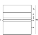
발광 다이오드 칩(1)의 효율을 향상시키기 위해, 상기 발광 다이오드 칩(1)은 방사선 배출 면(4)에 마주 놓인 후면에 국부적으로 미러 층(5)을 포함한다. 상기 미러 층(5)은 발광 다이오드 칩의 제 1 전기적 연결층(9)과 p-도핑된 반도체 영역(2b) 사이에 배치되어 있다. 미러 층(5)을 통해서는, 바람직하게 활성 층(3)으로부터 캐리어(19) 방향으로 방출되는 방사선이 방사선 배출 면(4) 쪽으로 반사된다.In order to improve the efficiency of the light emitting diode chip 1, the light emitting diode chip 1 comprises a
미러 층(5)은 반사 작용을 하는 콘택 층 시퀀스의 구성 요소이고, 상기 콘택 층 시퀀스는 상기 미러 층(5)과 제 1 전기적 연결층(9) 사이에 추가의 층들을 포함하며, 도 1에는 도면의 간략화를 위해 상기 추가의 층들 중 모든 층들이 도시되어 있지는 않다.The
반사 작용을 하는 콘택 층 시퀀스(10)의 구조는 도 2에 도시되어 있으며, 상기 도 2에는 도 1의 컷-아웃(A)의 상세도가 도시되어 있다. 은을 함유하는 미러 층(5)은 바람직하게 반도체 층 시퀀스(2)의 p-도핑된 영역(2b)에 직접 인접한다. 반도체 층 시퀀스(2)로부터 떨어져서 마주하는 측에서 미러 층(5) 상에는 기능 층(6)이 배치되어 있다. 상기 기능 층(6)은 반도체 층 시퀀스(2)에의 미러 층의 전기적 연결을 향상시키기 위해 그리고/또는 접착 상태를 향상시키기 위해 그리고/또는 부식을 감소시키기 위해 사용된다. 이러한 점들은 특히 기능 층(6)을 형성하는 재료가 적어도 부분적으로 미러 층(5) 내에도 포함됨으로써 달성된다. 특히 기능 층(6)의 재료는 미러 층(5) 내부로 확산될 수 있다.The structure of the reflective
미러 층(5) 내부로 기능 층(6)의 재료를 확산시키기 위하여, 발광 다이오드 칩(1)의 제조 공정 시 상기 기능 층(6)은 상기 미러 층(5)에 배치된 후에 바람직하게 온도 조절된다. 온도 조절은 바람직하게 200 ℃(200 ℃ 포함) 내지 400 ℃(400 ℃ 포함)의 온도, 특히 250 ℃(350 ℃ 포함) 내지 350 ℃(350 ℃ 포함)의 온도에서 이루어진다. 온도 프로세스에 대한 시간은 예를 들어 1분 내지 1시간에 이를 수 있다.In order to diffuse the material of the
바람직하게 기능 층(6)의 재료는, 상기 기능 층 재료가 대부분의 미러 층(5) 내에 포함되는 방식으로 미러 층(5) 내부로 확산된다. 특히 바람직하게는 상기 기능 층(6)의 재료가 전체 미러 층(5) 내에 포함되어 있다. 이러한 경우에는 기능 층(6)의 재료가 반도체 층 시퀀스(2)에 인접하는 미러 층(5)의 영역 내에도 포함되어 있다.Preferably the material of the
기능 층(6)의 재료가 미러 층(5) 내에도 포함됨으로써 미러 층(5)의 장기 안정성이 구현될 수 있다는 사실이 밝혀졌다. 특히 이러한 방식에 의해서 미러 층(5)의 부식이 감소되고 반도체 층 시퀀스(2) 상에서의 접착 상태가 개선된다. 또한, 상기와 같은 미러 층(5)은 반도체 층 시퀀스(2)의 반도체 재료에의 우수한 전기적 연결을 만들어 낸다.It has been found that the material of the
미러 층(5) 내에 포함된 기능 층(6)의 재료는 미러 층(5) 내부에서 농도 기울기를 가질 수 있다. 특히 확산 프로세스에 의해, 기능 층(6)의 재료 농도는 기능 층(6) 쪽을 향하는 측에서보다 반도체 층 시퀀스(2) 쪽을 향하는 미러 층(5)의 측에서 더 낮을 수 있다. 이 때문에 반도체 층 시퀀스(2)에 대한 경계면에 있는 은을 포함하는 미러 층(5)의 반사율이 단지 약간만 저하된다. 특히 미러 층(5)의 반사율은 상기 미러 층 내에 포함된 기능 층(6)의 추가 재료에 의해, 반도체 층 시퀀스(2)와 미러 층(5) 사이에 접착층이 삽입되는 경우보다 덜 저하된다.The material of the
백금으로 이루어진 기능 층(6)이 특히 바람직한 것으로 밝혀졌다. 물론 대안적으로 기능 층(6)이 니켈, 크롬, 팔라듐, 로듐 또는 예를 들어 ITO 또는 ZnO와 같은 투명 전도성 산화물을 포함하는 것도 생각할 수 있다. 기능 층(6)의 두께는 예를 들어 0.1 ㎚ 내지 1000 ㎚에 달할 수 있으며, 이 경우 미러 층(5)의 특히 우수한 안정성 개선은 10 ㎚(10 ㎚ 포함) 내지 100 ㎚(100 ㎚ 포함)의 두께를 갖는 기능 층(6)에 의해 달성된다.It has been found that the
반사 작용을 하는 콘택 층 시퀀스(10)에서 기능 층(6)에 다음에는 확산 배리어 층(7)이 후속되고, 상기 확산 배리어 층으로서는 바람직하게 티탄 층이 사용된다. 대안적으로 확산 배리어 층의 재료들로는 크롬, 니켈, 팔라듐, 질화 티탄 또는 질화 티탄 텅스텐이 있다. 확산 배리어 층(7)은 미러 층(5)의 재료, 특히 은 그리고 제 1 전기적 연결층(9)의 재료, 예컨대 금의 상호 확산을 방지한다. In the reflective
상기 확산 배리어 층(7) 다음에는 접착층(8)이 후속되는데, 상기 접착층에 의해서는 후속하는 제 1 전기적 연결층(9)의 접착 상태가 향상된다. 접착층(8)은 바람직하게 백금 층이고, 그러나 이 경우 대안적으로 티탄 또는 크롬도 상기 접착층의 재료로 적합하다,The
제 1 전기적 연결층(9)은 바람직하게 금 층이다. 대안적으로 상기 제 1 전기적 연결층은 전기 전도성이 우수한 다른 재료, 예를 들면 구리 또는 니켈로부터도 형성될 수 있다.The first
반사 작용을 하는 콘택 층 시퀀스(10)의 특히 바람직한 한 가지 실시 예에서, 기능 층(6)은 백금 층이고, 확산 배리어 층(7)은 티탄 층이며 그리고 접착층(8)은 백금 층이다. 티탄은 미러 층(5)과 제 1 전기적 연결층(9) 사이에서 매우 우수한 확산 배리어 효과를 갖는 것으로 밝혀졌으며, 이 경우 티탄 층을 둘러싸는 2개의 백금층은 상기 티탄 층을 부식 및/또는 산화로부터 매우 우수하게 보호한다.In one particularly preferred embodiment of the reflective
도 1에 도시된 바와 같이, 발광 다이오드 칩(1)은 제 2 전기적 연결층(15)을 포함하고, 상기 제 2 전기적 연결층을 통해서 발광 다이오드 칩(1)은 방사선 배출 면(4)에 마주 놓인 후면과 콘택팅 된다. 다시 말하자면, 제 1 전기적 연결층(9)뿐만 아니라 제 2 전기적 연결층(15)도 캐리어(19) 쪽을 향하는 발광 다이오드 칩(1)의 후면에 배치되어 있다. 이러한 배치가 갖는 장점은, 방사선 배출 면(4)이 전기적 연결층들을 갖지 않음으로써, 발광 다이오드 칩(1)으로부터 방출된 전자기 방사선(11)이 전기적 연결층들(9, 15)에 의해 차폐되지 않는다는 것이다.As shown in FIG. 1, the light emitting diode chip 1 comprises a second
제 1 전기적 연결층(9)은 바람직하게 반도체 층 시퀀스(2)의 p-도핑된 영역(2b)에 콘택팅 된다. 제 2 전기적 연결층(15)은 바람직하게 반도체 층 시퀀스(2)의 n-도핑된 영역(2a)에 콘택팅 된다. 이 목적을 위해 상기 제 2 전기적 연결층(15)은 발광 다이오드 칩(1)의 후면으로부터 하나 또는 다수의 관통구(21a, 21b)를 통과하여 반도체 층 시퀀스(2)의 n-도핑된 영역(2a)까지 리드 되어 있으며, 상기 관통구들은 반도체 층 시퀀스(2)의 p-도핑된 영역(2b)과 활성 층(3)을 통과한다. 단락을 방지하기 위하여, 제 2 전기적 연결층(15)은 관통구들(21a, 21b)의 영역에서 패시베이션 층(13)에 의해 활성 층(3) 및 반도체 층 시퀀스(2)의 p-도핑된 영역(2b)으로부터 절연되었다.The first electrically connecting
또한, 패시베이션 층(13)은 제 2 전기적 연결층(15)을 제 1 전기적 연결층(9)으로부터도 절연시킨다. 패시베이션 층(13)은 예를 들어 SiO2 또는 SiN과 같은 전기 절연 재료로부터 형성되었다. The
제 2 전기적 연결층(15)은 은을 함유하고 특히 관통구들(21a, 21b)의 영역에서 발광 다이오드 칩(1)으로부터 방출된 전자기 방사선(11)의 제 2 미러 층으로 기능 한다.The second
납땜 층(18)과 제 2 전기적 연결층(15) 사이에는 확산 배리어 층(17)이 배치되어 있다. 패시베이션 층(13), 제 2 전기적 연결층(15)과 확산 배리어 층(17) 사이에는 추가의 층들이 배치되어 있는데, 상기 추가의 층들은 도 1에서 도면의 간략화를 위해 도시되지 않았다. 상기 추가의 층들은 도 1의 컷-아웃(B)의 상세도를 보여주는 도 3에 도시되어 있다.A
은을 함유하고 제 2 미러 층으로서 작용하는 제 2 전기적 연결층(15)과 패시베이션 층(13) 사이에는 접착층(14)이 배치될 수 있다. 상기 접착층(14)으로서는 바람직하게 티탄 층이 사용된다. 접착층(14)은 선택적으로 생략될 수도 있다. An
패시베이션 층(13)에 마주 놓인 측에서, 제 2 전기적 연결층(15)에는 제 2 기능 층(16)이 배치되어 있으며, 상기 제 2 기능 층은 바람직하게 백금 층이다. 제 2 기능 층(16)은 그 작용 방식 및 바람직한 실시 예들의 측면에서 미러 층(5)과 관련하여 전술된 기능 층(6)과 상응한다. 특히 기능 층(16)의 재료는 제 2 전기적 연결층(15) 내에도 포함되어 있다.On the side opposite to the
층 시퀀스(12)에서, 기능 층(16)에는 바람직하게 질화 티탄 텅스텐을 함유하는 확산 배리어 층(17)이 뒤따른다. 확산 층(17)에는 납땜 층(18)이 뒤따르고 상기 납땜 층에 의해서는 발광 다이오드 칩(1)이 캐리어(19) 상에 납땜 되었다. 납땜 층(18)은 특히 AuSn을 함유할 수 있다. 확산 배리어 층(17)은, 납땜 층(18)의 구성 성분이 제 2 전기적 연결층(15) 내부로 확산되는 것을 방지하고 그리고 그 역도 마찬가지이다. In the
도 1에 도시된 발광 다이오드 칩의 캐리어(19)로서는 예를 들어 게르마늄-캐리어가 사용될 수 있다. 발광 다이오드 칩(1)으로부터 떨어져서 마주하는 캐리어의 후면에는 콘택 금속화층(20)이 배치될 수 있으며, 상기 콘택 금속화층에 의해 제 2 전기적 연결층(15)은 외부로 전기 접속된다. 제 1 전기적 연결층(9)은 예를 들어 본딩 패드(22) 및 본딩 와이어(23)에 의해 외부로 전기 접속될 수 있다.As the carrier 19 of the light emitting diode chip shown in Fig. 1, for example, germanium-carrier may be used. A
본 발명은 실시 예들을 참조하는 상세한 설명에 의해서 한정되지 않는다. 오히려 본 발명은 각각의 새로운 특징 그리고 상기 특징들의 각각의 조합을 포함하며, 특히 상기 특징 그리고 특징 조합 자체가 특허 청구의 범위 또는 실시 예들에 명시적으로 기재되어 있지 않더라도 각각의 특징 및 특징 조합은 특허 청구의 범위에 포함된 것으로 간주 된다. The invention is not limited by the detailed description with reference to the embodiments. Rather, the present invention includes each new feature and each combination of the above features, in particular each feature and feature combination is a patent even if the feature and feature combination itself are not expressly described in the claims or the embodiments. It is considered to be included in the claims.
Claims (14)
상기 발광 다이오드 칩(1)은 전면에 방사선 배출 면(4)을 구비하고,
상기 발광 다이오드 칩(1)은 상기 방사선 배출 면(4)에 마주 놓인 후면에 적어도 국부적으로 미러 층(5)을 구비하며, 상기 미러 층은 은을 함유하고,
상기 미러 층(5) 상에는, 미러 층(5)의 접착 상태를 향상시키기 위한 그리고/또는 부식을 감소시키기 위한 기능 층(6)이 배치되어 있으며,
상기 기능 층(6)을 형성하는 재료는 전체 미러 층(5) 내에도 분포되어 있고, 상기 기능 층(6)의 재료는 상기 미러 층(5) 내에서 농도 기울기를 가지며, 그리고
상기 미러 층(5) 내에서 상기 기능 층(6)의 재료 농도는 상기 기능 층(6)으로부터 상기 반도체 층 시퀀스(2) 방향으로 감소하는,
발광 다이오드 칩. A light emitting diode chip (1) comprising a semiconductor layer sequence (2) with an active layer (3) suitable for generating electromagnetic radiation (11),
The light emitting diode chip 1 has a radiation emitting surface 4 on its front surface,
The light emitting diode chip 1 has a mirror layer 5 at least locally on the rear surface facing the radiation emitting surface 4, the mirror layer containing silver,
On the mirror layer 5 a functional layer 6 is arranged for improving the adhesion state of the mirror layer 5 and / or for reducing corrosion,
The material forming the functional layer 6 is also distributed in the entire mirror layer 5, the material of the functional layer 6 has a concentration gradient in the mirror layer 5, and
The material concentration of the functional layer 6 in the mirror layer 5 decreases from the functional layer 6 in the direction of the semiconductor layer sequence 2,
Light emitting diode chip.
상기 미러 층(5)은 상기 반도체 층 시퀀스(2)에 직접 인접하는,
발광 다이오드 칩.The method of claim 1,
The mirror layer 5 is directly adjacent to the semiconductor layer sequence 2,
Light emitting diode chip.
상기 기능 층(6)은 백금을 함유하는,
발광 다이오드 칩.3. The method according to claim 1 or 2,
The functional layer 6 contains platinum
Light emitting diode chip.
상기 기능 층(6)은 니켈, 크롬, 팔라듐, 로듐 또는 투명 전도성 산화물을 함유하는,
발광 다이오드 칩.3. The method according to claim 1 or 2,
The functional layer 6 contains nickel, chromium, palladium, rhodium or transparent conductive oxides,
Light emitting diode chip.
상기 기능 층(6)은 0.1 ㎚ 내지 1000 ㎚의 두께를 갖는,
발광 다이오드 칩.The method according to any one of claims 1 to 4,
The functional layer 6 has a thickness of 0.1 nm to 1000 nm,
Light emitting diode chip.
상기 기능 층(6)은 10 ㎚ 내지 100 ㎚의 두께를 갖는,
발광 다이오드 칩.The method of claim 5, wherein
The functional layer 6 has a thickness of 10 nm to 100 nm,
Light emitting diode chip.
상기 미러 층(5)은 반사 작용을 하는 콘택 층 시퀀스(10)의 구성 요소이고, 상기 콘택 층 시퀀스는 상기 반도체 층 시퀀스(2)로부터 시작하여 하기에 언급된 순서대로 적어도
은을 함유하는 미러 층(5),
상기 미러 층(5)의 접착 상태를 향상시키기 위한 그리고/또는 부식을 감소시키기 위한 기능 층(6),
확산 배리어 층(7) 및
제 1 전기적 연결층(9)을 포함하는,
발광 다이오드 칩.7. The method according to any one of claims 1 to 6,
The mirror layer 5 is a component of the contact layer sequence 10 which is reflective and at least in the order mentioned below starting from the semiconductor layer sequence 2.
A mirror layer 5 containing silver,
A functional layer 6 for improving the adhesion state of the mirror layer 5 and / or for reducing corrosion,
Diffusion barrier layer 7 and
Comprising a first electrical connection layer 9,
Light emitting diode chip.
상기 제 1 전기적 연결층(9)은 금을 함유하는,
발광 다이오드 칩.The method of claim 7, wherein
The first electrical connection layer 9 contains gold,
Light emitting diode chip.
상기 확산 배리어 층(7)은 티탄, 크롬, 니켈, 팔라듐, 질화 티탄(titanium nitride) 또는 질화 티탄 텅스텐(titanium tungsten nitride)을 함유하는,
발광 다이오드 칩. 9. The method according to claim 7 or 8,
The diffusion barrier layer 7 contains titanium, chromium, nickel, palladium, titanium nitride or titanium tungsten nitride,
Light emitting diode chip.
상기 확산 배리어 층(7)과 제 1 전기적 연결층(9) 사이에 접착층(8)이 배치된,
발광 다이오드 칩.10. The method according to any one of claims 7 to 9,
An adhesive layer 8 is disposed between the diffusion barrier layer 7 and the first electrical connection layer 9,
Light emitting diode chip.
상기 접착층(8)은 백금, 티탄 또는 크롬을 함유하는,
발광 다이오드 칩.11. The method of claim 10,
The adhesive layer 8 contains platinum, titanium or chromium,
Light emitting diode chip.
상기 발광 다이오드 칩(1)은 제 1 전기적 연결층(9) 및 제 2 전기적 연결층(15)을 구비하고,
상기 제 1 전기적 연결층(9)과 제 2 전기적 연결층(15)은 상기 반도체 층 시퀀스(2)의 후면 쪽을 향하고 패시베이션 층(13)에 의해 전기적으로 서로 절연되어 있으며,
상기 제 2 전기적 연결층(15)의 부분 영역은 상기 반도체 층 시퀀스(2)의 후면으로부터 상기 활성 층(3)의 적어도 하나의 관통구(21a, 21b)를 통해 전면 방향으로 연장되고,
상기 제 2 전기적 연결층(15)은 은을 함유하고 제 2 미러 층으로서 기능 하며,
상기 제 2 전기적 연결층(15) 상에는, 제 2 전기적 연결층(15)의 접착 상태를 향상시키기 위한 그리고/또는 부식을 감소시키기 위한 제 2 기능 층(16)이 배치되어 있으며, 상기 제 2 기능 층(16)을 형성하는 재료가 상기 제 2 전기적 연결층 층(15) 내에도 함유되어 있는,
발광 다이오드 칩. 12. The method according to any one of claims 1 to 11,
The light emitting diode chip 1 has a first electrical connection layer 9 and a second electrical connection layer 15,
The first electrically connected layer 9 and the second electrically connected layer 15 face the back side of the semiconductor layer sequence 2 and are electrically insulated from each other by a passivation layer 13,
The partial region of the second electrical connection layer 15 extends from the backside of the semiconductor layer sequence 2 in the front direction through at least one through hole 21a, 21b of the active layer 3,
The second electrical connection layer 15 contains silver and functions as a second mirror layer,
On the second electrical connection layer 15, a second functional layer 16 is arranged to improve the adhesion state of the second electrical connection layer 15 and / or to reduce corrosion, and the second function The material forming the layer 16 is also contained in the second electrically connecting layer layer 15,
Light emitting diode chip.
상기 제 2 전기적 연결층(15)은 적어도 국부적으로 층 시퀀스(12)의 구성 요소이고, 상기 층 시퀀스는 하기에 언급된 순서대로 적어도
패시베이션 층(13),
제 2 전기적 연결층(15),
제 2 기능 층(16),
확산 배리어 층(17) 및
납땜 층(18)을 포함하는,
발광 다이오드 칩. 13. The method of claim 12,
The second electrically connecting layer 15 is at least locally a component of the layer sequence 12, the layer sequence being at least in the order mentioned below.
Passivation layer 13,
Second electrical connection layer 15,
Second functional layer 16,
Diffusion barrier layer 17 and
Comprising a solder layer 18,
Light emitting diode chip.
상기 발광 다이오드 칩(1)은 상기 방사선 배출 면(4)에 마주 놓인 측에서 상기 납땜 층(18)에 의해 기판(19)에 연결된,
발광 다이오드 칩.The method of claim 13,
The light emitting diode chip 1 is connected to the substrate 19 by the solder layer 18 on the side facing the radiation emitting surface 4,
Light emitting diode chip.
Applications Claiming Priority (3)
| Application Number | Priority Date | Filing Date | Title |
|---|---|---|---|
| DE102010009717A DE102010009717A1 (en) | 2010-03-01 | 2010-03-01 | LED chip |
| DE102010009717.9 | 2010-03-01 | ||
| PCT/EP2011/052233 WO2011107344A1 (en) | 2010-03-01 | 2011-02-15 | Light emitting diode chip |
Publications (1)
| Publication Number | Publication Date |
|---|---|
| KR20130036222A true KR20130036222A (en) | 2013-04-11 |
Family
ID=43743712
Family Applications (1)
| Application Number | Title | Priority Date | Filing Date |
|---|---|---|---|
| KR1020127025913A KR20130036222A (en) | 2010-03-01 | 2011-02-15 | Light emitting diode chip |
Country Status (8)
| Country | Link |
|---|---|
| US (1) | US8872209B2 (en) |
| EP (1) | EP2543083B1 (en) |
| JP (1) | JP2013521636A (en) |
| KR (1) | KR20130036222A (en) |
| CN (1) | CN102782886B (en) |
| DE (1) | DE102010009717A1 (en) |
| TW (1) | TWI459603B (en) |
| WO (1) | WO2011107344A1 (en) |
Cited By (1)
| Publication number | Priority date | Publication date | Assignee | Title |
|---|---|---|---|---|
| KR20150142737A (en) * | 2014-06-11 | 2015-12-23 | 엘지이노텍 주식회사 | Light emitting device and lighting system |
Families Citing this family (22)
| Publication number | Priority date | Publication date | Assignee | Title |
|---|---|---|---|---|
| DE102011054891B4 (en) | 2011-10-28 | 2017-10-19 | Osram Opto Semiconductors Gmbh | Method for severing a semiconductor device composite |
| KR101868537B1 (en) * | 2011-11-07 | 2018-06-19 | 엘지이노텍 주식회사 | Light emitting device and light emitting device package including the device |
| US9450152B2 (en) | 2012-05-29 | 2016-09-20 | Micron Technology, Inc. | Solid state transducer dies having reflective features over contacts and associated systems and methods |
| KR101946914B1 (en) * | 2012-06-08 | 2019-02-12 | 엘지이노텍 주식회사 | Light emitting device, light emitting device package, and light unit |
| DE102012107384A1 (en) * | 2012-08-10 | 2014-02-13 | Osram Opto Semiconductors Gmbh | Optoelectronic semiconductor component and method for producing a mirror region on a semiconductor body |
| DE102012108879B4 (en) * | 2012-09-20 | 2024-03-28 | OSRAM Opto Semiconductors Gesellschaft mit beschränkter Haftung | Optoelectronic semiconductor chip with several active areas arranged next to one another |
| DE102012110775A1 (en) * | 2012-11-09 | 2014-05-15 | Osram Opto Semiconductors Gmbh | Optoelectronic semiconductor chip and method for producing an optoelectronic semiconductor chip |
| DE102012111245A1 (en) * | 2012-11-21 | 2014-05-22 | Osram Opto Semiconductors Gmbh | Method for producing a connection region of an optoelectronic semiconductor chip |
| DE102013107531A1 (en) * | 2013-07-16 | 2015-01-22 | Osram Opto Semiconductors Gmbh | Optoelectronic semiconductor chip |
| DE102014202424A1 (en) | 2014-02-11 | 2015-08-13 | Osram Opto Semiconductors Gmbh | Optoelectronic component with a reflective layer sequence and method for generating a reflective layer sequence |
| CN106165128B (en) * | 2014-04-07 | 2018-11-09 | Lg 伊诺特有限公司 | Light-emitting component and lighting system |
| DE102014107123A1 (en) | 2014-05-20 | 2015-11-26 | Osram Opto Semiconductors Gmbh | Method for producing an optoelectronic semiconductor chip and optoelectronic semiconductor chip |
| JP2016054260A (en) | 2014-09-04 | 2016-04-14 | 株式会社東芝 | Semiconductor light-emitting element |
| JP6398541B2 (en) * | 2014-09-29 | 2018-10-03 | 日亜化学工業株式会社 | Lead frame and light emitting device |
| DE102016112291A1 (en) * | 2016-07-05 | 2018-01-11 | Osram Opto Semiconductors Gmbh | Optoelectronic semiconductor chip and method for producing an optoelectronic semiconductor chip |
| EP3537486A4 (en) * | 2016-11-03 | 2020-08-12 | LG Innotek Co., Ltd. | Semiconductor device and semiconductor device package including same |
| DE102017123154A1 (en) * | 2017-10-05 | 2019-04-11 | Osram Opto Semiconductors Gmbh | Method for producing an optoelectronic component and optoelectronic component |
| DE102017123242A1 (en) | 2017-10-06 | 2019-04-11 | Osram Opto Semiconductors Gmbh | Method for producing one or a plurality of semiconductor chips and semiconductor chip |
| DE102018128692A1 (en) * | 2018-11-15 | 2020-05-20 | Osram Opto Semiconductors Gmbh | Optoelectronic semiconductor component with first connection areas and optoelectronic device |
| DE102018132542A1 (en) | 2018-12-17 | 2020-06-18 | Osram Opto Semiconductors Gmbh | OPTOELECTRONIC LIGHTING DEVICE AND MANUFACTURING METHOD |
| CN110137201B (en) * | 2019-05-24 | 2021-06-25 | 厦门乾照光电股份有限公司 | Display screen lamp bead device, integrated diode chip and preparation method |
| DE102021201131A1 (en) * | 2021-02-08 | 2022-08-11 | OSRAM Opto Semiconductors Gesellschaft mit beschränkter Haftung | OPTOELECTRONIC SEMICONDUCTOR COMPONENT WITH A GOLD LAYER IN THE REGION |
Family Cites Families (18)
| Publication number | Priority date | Publication date | Assignee | Title |
|---|---|---|---|---|
| US6740906B2 (en) | 2001-07-23 | 2004-05-25 | Cree, Inc. | Light emitting diodes including modifications for submount bonding |
| US6888167B2 (en) | 2001-07-23 | 2005-05-03 | Cree, Inc. | Flip-chip bonding of light emitting devices and light emitting devices suitable for flip-chip bonding |
| TW577178B (en) | 2002-03-04 | 2004-02-21 | United Epitaxy Co Ltd | High efficient reflective metal layer of light emitting diode |
| TWI243488B (en) * | 2003-02-26 | 2005-11-11 | Osram Opto Semiconductors Gmbh | Electrical contact-area for optoelectronic semiconductor-chip and its production method |
| KR100585919B1 (en) * | 2004-01-15 | 2006-06-01 | 학교법인 포항공과대학교 | Gallium nitride-based ?? group compound semiconductor device and methed of producing the same |
| JP5011628B2 (en) | 2004-01-20 | 2012-08-29 | 日亜化学工業株式会社 | Semiconductor light emitting device |
| JP2006024750A (en) * | 2004-07-08 | 2006-01-26 | Matsushita Electric Ind Co Ltd | Light emitting element |
| KR100576870B1 (en) * | 2004-08-11 | 2006-05-10 | 삼성전기주식회사 | Nitride semiconductor light emitting diode and method of producing the same |
| US7259402B2 (en) * | 2004-09-22 | 2007-08-21 | Cree, Inc. | High efficiency group III nitride-silicon carbide light emitting diode |
| JP4923693B2 (en) * | 2006-04-17 | 2012-04-25 | 日亜化学工業株式会社 | Semiconductor light emitting device and semiconductor light emitting device |
| US8643195B2 (en) * | 2006-06-30 | 2014-02-04 | Cree, Inc. | Nickel tin bonding system for semiconductor wafers and devices |
| JP2008192782A (en) * | 2007-02-05 | 2008-08-21 | Toyota Central R&D Labs Inc | Electrode and iii nitride compound semiconductor light-emitting element using the electrode |
| DE102007022947B4 (en) * | 2007-04-26 | 2022-05-05 | OSRAM Opto Semiconductors Gesellschaft mit beschränkter Haftung | Optoelectronic semiconductor body and method for producing such |
| JP5139005B2 (en) * | 2007-08-22 | 2013-02-06 | 株式会社東芝 | Semiconductor light emitting device and semiconductor light emitting device |
| US20090250713A1 (en) * | 2008-04-04 | 2009-10-08 | Philips Lumileds Lighting Company, Llc | Reflective Contact for a Semiconductor Light Emitting Device |
| TWI389355B (en) | 2009-01-05 | 2013-03-11 | Epistar Corp | Light emitting semiconductor apparatus |
| DE102009033686A1 (en) | 2009-07-17 | 2011-01-20 | Osram Opto Semiconductors Gmbh | Optoelectronic semiconductor component and method for producing an inorganic optoelectronic semiconductor component |
| DE102010024079A1 (en) | 2010-06-17 | 2011-12-22 | Osram Opto Semiconductors Gmbh | Method for producing an optoelectronic semiconductor chip and optoelectronic semiconductor chip |
-
2010
- 2010-03-01 DE DE102010009717A patent/DE102010009717A1/en not_active Withdrawn
-
2011
- 2011-02-15 US US13/581,417 patent/US8872209B2/en not_active Expired - Fee Related
- 2011-02-15 WO PCT/EP2011/052233 patent/WO2011107344A1/en active Application Filing
- 2011-02-15 CN CN201180011835.1A patent/CN102782886B/en not_active Expired - Fee Related
- 2011-02-15 EP EP11703686.3A patent/EP2543083B1/en not_active Not-in-force
- 2011-02-15 KR KR1020127025913A patent/KR20130036222A/en not_active Application Discontinuation
- 2011-02-15 JP JP2012555354A patent/JP2013521636A/en active Pending
- 2011-02-25 TW TW100106364A patent/TWI459603B/en not_active IP Right Cessation
Cited By (1)
| Publication number | Priority date | Publication date | Assignee | Title |
|---|---|---|---|---|
| KR20150142737A (en) * | 2014-06-11 | 2015-12-23 | 엘지이노텍 주식회사 | Light emitting device and lighting system |
Also Published As
| Publication number | Publication date |
|---|---|
| TW201145611A (en) | 2011-12-16 |
| CN102782886A (en) | 2012-11-14 |
| EP2543083B1 (en) | 2017-10-11 |
| JP2013521636A (en) | 2013-06-10 |
| DE102010009717A1 (en) | 2011-09-01 |
| WO2011107344A1 (en) | 2011-09-09 |
| CN102782886B (en) | 2016-05-04 |
| US8872209B2 (en) | 2014-10-28 |
| US20130146910A1 (en) | 2013-06-13 |
| TWI459603B (en) | 2014-11-01 |
| EP2543083A1 (en) | 2013-01-09 |
Similar Documents
| Publication | Publication Date | Title |
|---|---|---|
| KR20130036222A (en) | Light emitting diode chip | |
| US10043958B2 (en) | Light emitting diode chip | |
| US7141828B2 (en) | Flip-chip light emitting diode with a thermally stable multiple layer reflective p-type contact | |
| KR100876737B1 (en) | Semiconductor light emitting device and manufacturing method thereof | |
| EP2763192B1 (en) | Nitride semiconductor element and method for producing same | |
| US9853188B2 (en) | Light-emitting diode chip with current spreading layer | |
| JP4644193B2 (en) | Semiconductor light emitting device | |
| US9099627B2 (en) | Method for producing group III nitride semiconductor light-emitting device | |
| KR101860973B1 (en) | Optoelectronic semiconductor chip | |
| US9299897B2 (en) | Optoelectronic semiconductor chip having a plurality of active regions arranged alongside one another | |
| US8710486B2 (en) | Optoelectronic semiconductor chip and method for manufacturing a contact structure for such a chip | |
| KR20070057681A (en) | Semiconductor light emitting device and method of manufacturing the same | |
| WO2006011362A1 (en) | Nitride semiconductor device | |
| CN110235258B (en) | Optoelectronic semiconductor chip | |
| EP1530242B1 (en) | Semiconductor light emitting device | |
| JP6911111B2 (en) | Manufacturing method of optoelectronic semiconductor chip and optoelectronic semiconductor chip | |
| US7242025B2 (en) | Radiation emitting semiconductor component having a nitride compound semiconductor body and a contact metallization layer on its surface | |
| JP2011517084A (en) | Reflective contacts for semiconductor light emitting devices | |
| CN110034219B (en) | Light emitting diode and method of manufacturing the same | |
| KR20140030855A (en) | Semiconductor light emitting device |
Legal Events
| Date | Code | Title | Description |
|---|---|---|---|
| WITN | Application deemed withdrawn, e.g. because no request for examination was filed or no examination fee was paid |