KR20120011786A - Display method and device - Google Patents
Display method and device Download PDFInfo
- Publication number
- KR20120011786A KR20120011786A KR1020110068933A KR20110068933A KR20120011786A KR 20120011786 A KR20120011786 A KR 20120011786A KR 1020110068933 A KR1020110068933 A KR 1020110068933A KR 20110068933 A KR20110068933 A KR 20110068933A KR 20120011786 A KR20120011786 A KR 20120011786A
- Authority
- KR
- South Korea
- Prior art keywords
- particles
- mode
- electric field
- light
- color
- Prior art date
Links
Images


Classifications
-
- G—PHYSICS
- G02—OPTICS
- G02F—OPTICAL DEVICES OR ARRANGEMENTS FOR THE CONTROL OF LIGHT BY MODIFICATION OF THE OPTICAL PROPERTIES OF THE MEDIA OF THE ELEMENTS INVOLVED THEREIN; NON-LINEAR OPTICS; FREQUENCY-CHANGING OF LIGHT; OPTICAL LOGIC ELEMENTS; OPTICAL ANALOGUE/DIGITAL CONVERTERS
- G02F1/00—Devices or arrangements for the control of the intensity, colour, phase, polarisation or direction of light arriving from an independent light source, e.g. switching, gating or modulating; Non-linear optics
- G02F1/01—Devices or arrangements for the control of the intensity, colour, phase, polarisation or direction of light arriving from an independent light source, e.g. switching, gating or modulating; Non-linear optics for the control of the intensity, phase, polarisation or colour
- G02F1/165—Devices or arrangements for the control of the intensity, colour, phase, polarisation or direction of light arriving from an independent light source, e.g. switching, gating or modulating; Non-linear optics for the control of the intensity, phase, polarisation or colour based on translational movement of particles in a fluid under the influence of an applied field
- G02F1/1685—Operation of cells; Circuit arrangements affecting the entire cell
-
- B—PERFORMING OPERATIONS; TRANSPORTING
- B82—NANOTECHNOLOGY
- B82Y—SPECIFIC USES OR APPLICATIONS OF NANOSTRUCTURES; MEASUREMENT OR ANALYSIS OF NANOSTRUCTURES; MANUFACTURE OR TREATMENT OF NANOSTRUCTURES
- B82Y20/00—Nanooptics, e.g. quantum optics or photonic crystals
-
- G—PHYSICS
- G02—OPTICS
- G02B—OPTICAL ELEMENTS, SYSTEMS OR APPARATUS
- G02B5/00—Optical elements other than lenses
- G02B5/20—Filters
- G02B5/22—Absorbing filters
- G02B5/24—Liquid filters
-
- G—PHYSICS
- G02—OPTICS
- G02F—OPTICAL DEVICES OR ARRANGEMENTS FOR THE CONTROL OF LIGHT BY MODIFICATION OF THE OPTICAL PROPERTIES OF THE MEDIA OF THE ELEMENTS INVOLVED THEREIN; NON-LINEAR OPTICS; FREQUENCY-CHANGING OF LIGHT; OPTICAL LOGIC ELEMENTS; OPTICAL ANALOGUE/DIGITAL CONVERTERS
- G02F1/00—Devices or arrangements for the control of the intensity, colour, phase, polarisation or direction of light arriving from an independent light source, e.g. switching, gating or modulating; Non-linear optics
- G02F1/01—Devices or arrangements for the control of the intensity, colour, phase, polarisation or direction of light arriving from an independent light source, e.g. switching, gating or modulating; Non-linear optics for the control of the intensity, phase, polarisation or colour
- G02F1/165—Devices or arrangements for the control of the intensity, colour, phase, polarisation or direction of light arriving from an independent light source, e.g. switching, gating or modulating; Non-linear optics for the control of the intensity, phase, polarisation or colour based on translational movement of particles in a fluid under the influence of an applied field
- G02F1/166—Devices or arrangements for the control of the intensity, colour, phase, polarisation or direction of light arriving from an independent light source, e.g. switching, gating or modulating; Non-linear optics for the control of the intensity, phase, polarisation or colour based on translational movement of particles in a fluid under the influence of an applied field characterised by the electro-optical or magneto-optical effect
- G02F1/167—Devices or arrangements for the control of the intensity, colour, phase, polarisation or direction of light arriving from an independent light source, e.g. switching, gating or modulating; Non-linear optics for the control of the intensity, phase, polarisation or colour based on translational movement of particles in a fluid under the influence of an applied field characterised by the electro-optical or magneto-optical effect by electrophoresis
-
- G—PHYSICS
- G02—OPTICS
- G02F—OPTICAL DEVICES OR ARRANGEMENTS FOR THE CONTROL OF LIGHT BY MODIFICATION OF THE OPTICAL PROPERTIES OF THE MEDIA OF THE ELEMENTS INVOLVED THEREIN; NON-LINEAR OPTICS; FREQUENCY-CHANGING OF LIGHT; OPTICAL LOGIC ELEMENTS; OPTICAL ANALOGUE/DIGITAL CONVERTERS
- G02F1/00—Devices or arrangements for the control of the intensity, colour, phase, polarisation or direction of light arriving from an independent light source, e.g. switching, gating or modulating; Non-linear optics
- G02F1/01—Devices or arrangements for the control of the intensity, colour, phase, polarisation or direction of light arriving from an independent light source, e.g. switching, gating or modulating; Non-linear optics for the control of the intensity, phase, polarisation or colour
- G02F1/165—Devices or arrangements for the control of the intensity, colour, phase, polarisation or direction of light arriving from an independent light source, e.g. switching, gating or modulating; Non-linear optics for the control of the intensity, phase, polarisation or colour based on translational movement of particles in a fluid under the influence of an applied field
- G02F1/1675—Constructional details
- G02F1/1676—Electrodes
-
- G—PHYSICS
- G02—OPTICS
- G02F—OPTICAL DEVICES OR ARRANGEMENTS FOR THE CONTROL OF LIGHT BY MODIFICATION OF THE OPTICAL PROPERTIES OF THE MEDIA OF THE ELEMENTS INVOLVED THEREIN; NON-LINEAR OPTICS; FREQUENCY-CHANGING OF LIGHT; OPTICAL LOGIC ELEMENTS; OPTICAL ANALOGUE/DIGITAL CONVERTERS
- G02F1/00—Devices or arrangements for the control of the intensity, colour, phase, polarisation or direction of light arriving from an independent light source, e.g. switching, gating or modulating; Non-linear optics
- G02F1/01—Devices or arrangements for the control of the intensity, colour, phase, polarisation or direction of light arriving from an independent light source, e.g. switching, gating or modulating; Non-linear optics for the control of the intensity, phase, polarisation or colour
- G02F1/17—Devices or arrangements for the control of the intensity, colour, phase, polarisation or direction of light arriving from an independent light source, e.g. switching, gating or modulating; Non-linear optics for the control of the intensity, phase, polarisation or colour based on variable-absorption elements not provided for in groups G02F1/015 - G02F1/169
-
- G—PHYSICS
- G02—OPTICS
- G02F—OPTICAL DEVICES OR ARRANGEMENTS FOR THE CONTROL OF LIGHT BY MODIFICATION OF THE OPTICAL PROPERTIES OF THE MEDIA OF THE ELEMENTS INVOLVED THEREIN; NON-LINEAR OPTICS; FREQUENCY-CHANGING OF LIGHT; OPTICAL LOGIC ELEMENTS; OPTICAL ANALOGUE/DIGITAL CONVERTERS
- G02F1/00—Devices or arrangements for the control of the intensity, colour, phase, polarisation or direction of light arriving from an independent light source, e.g. switching, gating or modulating; Non-linear optics
- G02F1/01—Devices or arrangements for the control of the intensity, colour, phase, polarisation or direction of light arriving from an independent light source, e.g. switching, gating or modulating; Non-linear optics for the control of the intensity, phase, polarisation or colour
- G02F1/21—Devices or arrangements for the control of the intensity, colour, phase, polarisation or direction of light arriving from an independent light source, e.g. switching, gating or modulating; Non-linear optics for the control of the intensity, phase, polarisation or colour by interference
-
- G—PHYSICS
- G02—OPTICS
- G02F—OPTICAL DEVICES OR ARRANGEMENTS FOR THE CONTROL OF LIGHT BY MODIFICATION OF THE OPTICAL PROPERTIES OF THE MEDIA OF THE ELEMENTS INVOLVED THEREIN; NON-LINEAR OPTICS; FREQUENCY-CHANGING OF LIGHT; OPTICAL LOGIC ELEMENTS; OPTICAL ANALOGUE/DIGITAL CONVERTERS
- G02F1/00—Devices or arrangements for the control of the intensity, colour, phase, polarisation or direction of light arriving from an independent light source, e.g. switching, gating or modulating; Non-linear optics
- G02F1/01—Devices or arrangements for the control of the intensity, colour, phase, polarisation or direction of light arriving from an independent light source, e.g. switching, gating or modulating; Non-linear optics for the control of the intensity, phase, polarisation or colour
- G02F1/23—Devices or arrangements for the control of the intensity, colour, phase, polarisation or direction of light arriving from an independent light source, e.g. switching, gating or modulating; Non-linear optics for the control of the intensity, phase, polarisation or colour for the control of the colour
- G02F1/25—Devices or arrangements for the control of the intensity, colour, phase, polarisation or direction of light arriving from an independent light source, e.g. switching, gating or modulating; Non-linear optics for the control of the intensity, phase, polarisation or colour for the control of the colour as to hue or predominant wavelength
-
- G—PHYSICS
- G09—EDUCATION; CRYPTOGRAPHY; DISPLAY; ADVERTISING; SEALS
- G09G—ARRANGEMENTS OR CIRCUITS FOR CONTROL OF INDICATING DEVICES USING STATIC MEANS TO PRESENT VARIABLE INFORMATION
- G09G3/00—Control arrangements or circuits, of interest only in connection with visual indicators other than cathode-ray tubes
- G09G3/20—Control arrangements or circuits, of interest only in connection with visual indicators other than cathode-ray tubes for presentation of an assembly of a number of characters, e.g. a page, by composing the assembly by combination of individual elements arranged in a matrix no fixed position being assigned to or needed to be assigned to the individual characters or partial characters
- G09G3/2003—Display of colours
-
- G—PHYSICS
- G09—EDUCATION; CRYPTOGRAPHY; DISPLAY; ADVERTISING; SEALS
- G09G—ARRANGEMENTS OR CIRCUITS FOR CONTROL OF INDICATING DEVICES USING STATIC MEANS TO PRESENT VARIABLE INFORMATION
- G09G3/00—Control arrangements or circuits, of interest only in connection with visual indicators other than cathode-ray tubes
- G09G3/20—Control arrangements or circuits, of interest only in connection with visual indicators other than cathode-ray tubes for presentation of an assembly of a number of characters, e.g. a page, by composing the assembly by combination of individual elements arranged in a matrix no fixed position being assigned to or needed to be assigned to the individual characters or partial characters
- G09G3/34—Control arrangements or circuits, of interest only in connection with visual indicators other than cathode-ray tubes for presentation of an assembly of a number of characters, e.g. a page, by composing the assembly by combination of individual elements arranged in a matrix no fixed position being assigned to or needed to be assigned to the individual characters or partial characters by control of light from an independent source
- G09G3/3433—Control arrangements or circuits, of interest only in connection with visual indicators other than cathode-ray tubes for presentation of an assembly of a number of characters, e.g. a page, by composing the assembly by combination of individual elements arranged in a matrix no fixed position being assigned to or needed to be assigned to the individual characters or partial characters by control of light from an independent source using light modulating elements actuated by an electric field and being other than liquid crystal devices and electrochromic devices
- G09G3/344—Control arrangements or circuits, of interest only in connection with visual indicators other than cathode-ray tubes for presentation of an assembly of a number of characters, e.g. a page, by composing the assembly by combination of individual elements arranged in a matrix no fixed position being assigned to or needed to be assigned to the individual characters or partial characters by control of light from an independent source using light modulating elements actuated by an electric field and being other than liquid crystal devices and electrochromic devices based on particles moving in a fluid or in a gas, e.g. electrophoretic devices
- G09G3/3446—Control arrangements or circuits, of interest only in connection with visual indicators other than cathode-ray tubes for presentation of an assembly of a number of characters, e.g. a page, by composing the assembly by combination of individual elements arranged in a matrix no fixed position being assigned to or needed to be assigned to the individual characters or partial characters by control of light from an independent source using light modulating elements actuated by an electric field and being other than liquid crystal devices and electrochromic devices based on particles moving in a fluid or in a gas, e.g. electrophoretic devices with more than two electrodes controlling the modulating element
-
- G—PHYSICS
- G02—OPTICS
- G02F—OPTICAL DEVICES OR ARRANGEMENTS FOR THE CONTROL OF LIGHT BY MODIFICATION OF THE OPTICAL PROPERTIES OF THE MEDIA OF THE ELEMENTS INVOLVED THEREIN; NON-LINEAR OPTICS; FREQUENCY-CHANGING OF LIGHT; OPTICAL LOGIC ELEMENTS; OPTICAL ANALOGUE/DIGITAL CONVERTERS
- G02F1/00—Devices or arrangements for the control of the intensity, colour, phase, polarisation or direction of light arriving from an independent light source, e.g. switching, gating or modulating; Non-linear optics
- G02F1/01—Devices or arrangements for the control of the intensity, colour, phase, polarisation or direction of light arriving from an independent light source, e.g. switching, gating or modulating; Non-linear optics for the control of the intensity, phase, polarisation or colour
- G02F1/165—Devices or arrangements for the control of the intensity, colour, phase, polarisation or direction of light arriving from an independent light source, e.g. switching, gating or modulating; Non-linear optics for the control of the intensity, phase, polarisation or colour based on translational movement of particles in a fluid under the influence of an applied field
- G02F1/1675—Constructional details
- G02F1/1676—Electrodes
- G02F1/16762—Electrodes having three or more electrodes per pixel
-
- G—PHYSICS
- G02—OPTICS
- G02F—OPTICAL DEVICES OR ARRANGEMENTS FOR THE CONTROL OF LIGHT BY MODIFICATION OF THE OPTICAL PROPERTIES OF THE MEDIA OF THE ELEMENTS INVOLVED THEREIN; NON-LINEAR OPTICS; FREQUENCY-CHANGING OF LIGHT; OPTICAL LOGIC ELEMENTS; OPTICAL ANALOGUE/DIGITAL CONVERTERS
- G02F2201/00—Constructional arrangements not provided for in groups G02F1/00 - G02F7/00
- G02F2201/44—Arrangements combining different electro-active layers, e.g. electrochromic, liquid crystal or electroluminescent layers
-
- G—PHYSICS
- G02—OPTICS
- G02F—OPTICAL DEVICES OR ARRANGEMENTS FOR THE CONTROL OF LIGHT BY MODIFICATION OF THE OPTICAL PROPERTIES OF THE MEDIA OF THE ELEMENTS INVOLVED THEREIN; NON-LINEAR OPTICS; FREQUENCY-CHANGING OF LIGHT; OPTICAL LOGIC ELEMENTS; OPTICAL ANALOGUE/DIGITAL CONVERTERS
- G02F2202/00—Materials and properties
- G02F2202/32—Photonic crystals
-
- G—PHYSICS
- G02—OPTICS
- G02F—OPTICAL DEVICES OR ARRANGEMENTS FOR THE CONTROL OF LIGHT BY MODIFICATION OF THE OPTICAL PROPERTIES OF THE MEDIA OF THE ELEMENTS INVOLVED THEREIN; NON-LINEAR OPTICS; FREQUENCY-CHANGING OF LIGHT; OPTICAL LOGIC ELEMENTS; OPTICAL ANALOGUE/DIGITAL CONVERTERS
- G02F2203/00—Function characteristic
- G02F2203/05—Function characteristic wavelength dependent
- G02F2203/055—Function characteristic wavelength dependent wavelength filtering
-
- G—PHYSICS
- G02—OPTICS
- G02F—OPTICAL DEVICES OR ARRANGEMENTS FOR THE CONTROL OF LIGHT BY MODIFICATION OF THE OPTICAL PROPERTIES OF THE MEDIA OF THE ELEMENTS INVOLVED THEREIN; NON-LINEAR OPTICS; FREQUENCY-CHANGING OF LIGHT; OPTICAL LOGIC ELEMENTS; OPTICAL ANALOGUE/DIGITAL CONVERTERS
- G02F2203/00—Function characteristic
- G02F2203/34—Colour display without the use of colour mosaic filters
-
- G—PHYSICS
- G09—EDUCATION; CRYPTOGRAPHY; DISPLAY; ADVERTISING; SEALS
- G09G—ARRANGEMENTS OR CIRCUITS FOR CONTROL OF INDICATING DEVICES USING STATIC MEANS TO PRESENT VARIABLE INFORMATION
- G09G2300/00—Aspects of the constitution of display devices
- G09G2300/08—Active matrix structure, i.e. with use of active elements, inclusive of non-linear two terminal elements, in the pixels together with light emitting or modulating elements
-
- G—PHYSICS
- G09—EDUCATION; CRYPTOGRAPHY; DISPLAY; ADVERTISING; SEALS
- G09G—ARRANGEMENTS OR CIRCUITS FOR CONTROL OF INDICATING DEVICES USING STATIC MEANS TO PRESENT VARIABLE INFORMATION
- G09G2310/00—Command of the display device
- G09G2310/06—Details of flat display driving waveforms
- G09G2310/061—Details of flat display driving waveforms for resetting or blanking
-
- G—PHYSICS
- G09—EDUCATION; CRYPTOGRAPHY; DISPLAY; ADVERTISING; SEALS
- G09G—ARRANGEMENTS OR CIRCUITS FOR CONTROL OF INDICATING DEVICES USING STATIC MEANS TO PRESENT VARIABLE INFORMATION
- G09G2320/00—Control of display operating conditions
- G09G2320/02—Improving the quality of display appearance
- G09G2320/0252—Improving the response speed
-
- G—PHYSICS
- G09—EDUCATION; CRYPTOGRAPHY; DISPLAY; ADVERTISING; SEALS
- G09G—ARRANGEMENTS OR CIRCUITS FOR CONTROL OF INDICATING DEVICES USING STATIC MEANS TO PRESENT VARIABLE INFORMATION
- G09G2320/00—Control of display operating conditions
- G09G2320/02—Improving the quality of display appearance
- G09G2320/0257—Reduction of after-image effects
-
- G—PHYSICS
- G09—EDUCATION; CRYPTOGRAPHY; DISPLAY; ADVERTISING; SEALS
- G09G—ARRANGEMENTS OR CIRCUITS FOR CONTROL OF INDICATING DEVICES USING STATIC MEANS TO PRESENT VARIABLE INFORMATION
- G09G2320/00—Control of display operating conditions
- G09G2320/06—Adjustment of display parameters
- G09G2320/0626—Adjustment of display parameters for control of overall brightness
- G09G2320/0646—Modulation of illumination source brightness and image signal correlated to each other
-
- G—PHYSICS
- G09—EDUCATION; CRYPTOGRAPHY; DISPLAY; ADVERTISING; SEALS
- G09G—ARRANGEMENTS OR CIRCUITS FOR CONTROL OF INDICATING DEVICES USING STATIC MEANS TO PRESENT VARIABLE INFORMATION
- G09G2320/00—Control of display operating conditions
- G09G2320/06—Adjustment of display parameters
- G09G2320/0666—Adjustment of display parameters for control of colour parameters, e.g. colour temperature
Landscapes
- Physics & Mathematics (AREA)
- Nonlinear Science (AREA)
- General Physics & Mathematics (AREA)
- Optics & Photonics (AREA)
- Engineering & Computer Science (AREA)
- Chemical & Material Sciences (AREA)
- Computer Hardware Design (AREA)
- Theoretical Computer Science (AREA)
- Life Sciences & Earth Sciences (AREA)
- Health & Medical Sciences (AREA)
- Chemical Kinetics & Catalysis (AREA)
- Electrochemistry (AREA)
- Molecular Biology (AREA)
- Nanotechnology (AREA)
- Crystallography & Structural Chemistry (AREA)
- Biophysics (AREA)
- Electrochromic Elements, Electrophoresis, Or Variable Reflection Or Absorption Elements (AREA)
- Liquid Crystal (AREA)
- Control Of Indicators Other Than Cathode Ray Tubes (AREA)
Abstract
Description
본 발명은 전반적으로 표시 방법 및 장치에 관한 것이다. 보다 상세하게는, 본 발명은 광 결정 반사 모드(photonic crystal reflection mode), 고유색 반사 모드(unique color reflection mode) 및 투과도 조절 모드(transmittance tuning mode) 중 적어도 2 개의 모드가 동일한 단일 화소 내에서 서로 전환 가능하게 되는 구현되는 표시 방법 및 장치에 관한 것이다.
The present invention relates generally to display methods and apparatus. More specifically, the present invention provides that at least two modes of photonic crystal reflection mode, unique color reflection mode, and transmittance tuning mode are switched to each other within the same single pixel. The present invention relates to an implemented display method and apparatus that is enabled.
최근 차세대 디스플레이에 대한 연구 및 개발이 활발하게 이루어지면서 다양한 종류의 디스플레이가 소개되고 있다. 차세대 디스플레이의 대표적인 예로서 전자 잉크(electronic-ink)를 들 수 있다. 전자 잉크는 각각 음전하 및 양전하를 갖는 특정 색(예를 들면, 각각 검은색 및 흰색)의 입자에 전기장을 인가하여 상기 특정 색을 표시하는 디스플레이로서, 전력 소모를 줄이고 플렉서블(flexible) 디스플레이를 가능하게 하는 장점을 갖고 있다. 다만, 전자 잉크에 의할 경우, 입자의 색이 특정 색으로 고정되어 있기 때문에 다양한 색을 표현하기 어렵다는 한계가 있다. 한편, 디스플레이와 함께 사용되어 디스플레이로부터 반사되거나 디스플레이로 입사되는 광을 투과 또는 차단시키는 기능을 하는 광 투과도 조절 장치가 소개된 바 있다. 종래의 광 투과도 조절 장치는 광의 투과를 제어하는 기능을 수행하는 기계적인 셔터를 포함하는 등 구조가 복잡하여 제조시간과 제조비용이 지나치게 높은 문제점이 있었다.Recently, as research and development on next-generation displays have been actively conducted, various kinds of displays have been introduced. An example of a next-generation display is electronic ink. The electronic ink is a display that displays the specific color by applying an electric field to particles of a specific color (eg, black and white, respectively) having negative and positive charges, respectively, which reduces power consumption and enables a flexible display. Has the advantage of. However, in the case of the electronic ink, since the color of the particles is fixed to a specific color, it is difficult to express various colors. On the other hand, there has been introduced a light transmittance adjusting device that is used in conjunction with the display to transmit or block the light reflected from the display or incident on the display. Conventional light transmittance adjusting device has a complicated structure such as a mechanical shutter that performs a function of controlling the transmission of light has a problem that the manufacturing time and manufacturing cost is too high.
따라서, 표시 영역에서 간단한 구조로 해서 다양한 색상 및/또는 투과도가 간단한 방식으로 해서 조절될 수 있는 방식이 제공될 필요가 있다.
Therefore, there is a need to provide a manner in which various colors and / or transmittances can be adjusted in a simple manner with a simple structure in the display area.
본 발명은 다양한 색상 및/또는 투과도가 동일한 단일 화소 내에서 간단한 방식 및 구조로 해서 구현되는 표시 방법 및 장치를 제공한다.The present invention provides a display method and apparatus which are implemented in a simple manner and structure within a single pixel having various colors and / or transmittances having the same.
본 발명은 다양한 색상, 투과도, 명도 및/또는 채도가 간단한 방식 및 구조로 해서 조절될 수 있는 표시 방법 및 장치를 제공한다.The present invention provides a display method and apparatus in which various colors, transmittances, brightnesses and / or saturations can be adjusted in a simple manner and structure.
본 발명은 입자 간격을 더욱 규칙적으로 배열시켜서 입자로부터 반사되는 광의 파장의 강도가 개선되는 표시 방법 및 장치를 제공한다. The present invention provides a display method and apparatus in which the particle spacing is arranged more regularly so that the intensity of the wavelength of light reflected from the particles is improved.
본 발명은 상기 표시 방법의 단계들을 수행하는 프로그램 코드를 기록한 머신 판독 가능한 기록 매체(machine readable storage medium)를 제공한다.
The present invention provides a machine readable storage medium on which program code for performing the steps of the display method is recorded.
본 발명의 일 측면에 따라서, 복수의 입자가 용매에 분산된 용액을 포함하는 표시부에 전극을 통하여 전기장을 인가하고, 상기 전기장의 세기, 방향, 인가 회수, 인가 시간 및 인가 위치 중 적어도 하나를 조절하여 상기 입자들의 간격, 위치 및 배열 중 적어도 하나를 제어하되, 상기 입자들의 간격을 제어함으로써 상기 간격이 제어된 입자들로부터 반사되는 광의 파장을 조절하는 제 1 모드와, 상기 입자들의 위치를 제어함으로써 상기 입자, 상기 용매, 상기 용액 및 상기 전극 중 적어도 하나의 컬러가 표시되는 제 2 모드를 상기 표시부의 동일한 단일 화소 내에서 서로 전환 가능하게 선택적으로 구현하는 표시 방법이 제공된다.According to an aspect of the present invention, the electric field is applied to the display unit including a solution in which a plurality of particles are dispersed in a solvent, and the at least one of the intensity, the direction, the number of times of application, the application time, and the application position of the electric field are adjusted. Controlling at least one of the spacing, position and arrangement of the particles, controlling the spacing of the particles, thereby controlling a wavelength of light reflected from the controlled particles, and by controlling the position of the particles. A display method is provided in which a second mode in which at least one color of the particles, the solvent, the solution, and the electrode are displayed is selectively switched to each other within the same single pixel of the display unit.
본 발명의 일 측면에 따라서, 복수의 입자가 용매에 분산된 용액을 포함하는 표시부에 전극을 통하여 전기장을 인가하고, 상기 전기장의 세기, 방향, 인가 회수, 인가 위치 및 인가 시간 중 적어도 하나를 조절하여 상기 입자들의 간격, 위치 및 배열 중 적어도 하나를 제어하되, 상기 입자들의 간격을 제어함으로써 상기 간격이 제어된 입자로부터 반사되는 광의 파장을 조절하는 제 1 모드와, 상기 입자들의 간격, 위치 또는 배열을 제어함으로써 상기 용액을 투과하는 광의 투과도를 조절하는 제 2 모드를 상기 표시부의 동일한 단일 화소 내에서 서로 전환 가능하게 선택적으로 구현하는 표시 방법이 제공된다.According to an aspect of the present invention, the electric field is applied to the display unit including a solution in which a plurality of particles are dispersed in a solvent through an electrode, and at least one of the intensity, the direction, the number of times of application, the application position and the application time of the electric field are adjusted. And controlling at least one of the spacing, position, and arrangement of the particles, wherein the spacing of the particles controls the first mode to control the wavelength of light reflected from the controlled particles, and the spacing, position, or arrangement of the particles. There is provided a display method of selectively implementing a second mode for controlling the transmittance of light passing through the solution so as to be switchable with each other within the same single pixel of the display unit.
본 발명의 일 측면에 따라서, 복수의 입자가 용매에 분산된 용액을 포함하는 표시부에 전극을 통하여 전기장을 인가하고, 상기 전기장의 세기, 방향, 인가 회수, 인가 위치 및 인가 시간 중 적어도 하나를 조절하여 상기 입자들의 간격, 위치 및 배열 중 적어도 하나를 제어하되, 상기 입자들의 위치를 제어함으로써 상기 입자, 상기 용매, 상기 용액 및 상기 전극 중 적어도 하나의 컬러가 표시되는 제 1 모드와, 상기 입자들의 간격, 위치 또는 배열을 제어함으로써 상기 용액을 투과하는 광의 투과도를 조절하는 제 2 모드를 상기 표시부의 동일한 단일 화소 내에서 서로 전환 가능하게 선택적으로 구현하는 표시 방법이 제공된다.According to an aspect of the present invention, the electric field is applied to the display unit including a solution in which a plurality of particles are dispersed in a solvent through an electrode, and at least one of the intensity, the direction, the number of times of application, the application position and the application time of the electric field are adjusted. A first mode in which the color of at least one of the particles, the solvent, the solution, and the electrode is displayed by controlling at least one of the spacing, position and arrangement of the particles, by controlling the position of the particles; A display method is provided that selectively implements a second mode for controlling the transmittance of light passing through the solution by controlling the interval, position or arrangement so as to be switchable from one another within the same single pixel of the display unit.
본 발명의 일 측면에 따라서, 복수의 입자가 용매에 분산된 용액을 포함하는 표시부에 전극을 통하여 전기장을 인가하고, 상기 전기장의 세기, 방향, 인가 회수, 인가 위치 및 인가 시간 중 적어도 하나를 조절하여 상기 입자들의 간격, 위치 및 배열 중 적어도 하나를 제어하되, 상기 입자들의 간격을 제어함으로써 상기 간격이 제어된 입자들로부터 반사되는 광의 파장을 조절하는 제 1 모드와, 상기 입자들의 위치를 제어함으로써 상기 입자, 상기 용매, 상기 용액 및 상기 전극 중 적어도 하나의 컬러가 표시되는 제 2 모드와, 상기 입자들의 간격, 위치 또는 배열을 제어함으로써 상기 용액을 투과하는 광의 투과도를 조절하는 제 3 모드를 상기 표시부의 동일한 단일 화소 내에서 서로 전환 가능하게 선택적으로 구현하는 표시 방법이 제공된다.According to an aspect of the present invention, the electric field is applied to the display unit including a solution in which a plurality of particles are dispersed in a solvent through an electrode, and at least one of the intensity, the direction, the number of times of application, the application position and the application time of the electric field are adjusted. Controlling at least one of the spacing, position and arrangement of the particles, controlling the spacing of the particles, thereby controlling a wavelength of light reflected from the controlled particles, and by controlling the position of the particles. And a second mode in which at least one color of the particles, the solvent, the solution, and the electrode is displayed, and a third mode in which the transmittance of the light passing through the solution is controlled by controlling the interval, position, or arrangement of the particles. A display method is provided that selectively implements switchable each other within the same single pixel of a display unit.
일 측면에 따라서, 적어도 하나가 투명한 적어도 2 개의 서로 대향하는 전극 간에 복수의 입자가 용매에 분산된 용액을 포함하는 표시부와, 상기 전극에 인가되는 전기장의 세기, 방향, 인가 회수, 인가 시간 및 인가 위치 중 적어도 하나를 조절하여 상기 입자들의 간격, 위치 및 배열 중 적어도 하나를 제어하는 제어부를 포함하며, 상기 제어부는 상기 입자들의 간격을 제어함으로써 상기 간격이 제어된 입자들로부터 반사되는 광의 파장을 조절하는 제 1 모드와, 상기 입자들의 위치를 제어함으로써 상기 입자, 상기 용매, 상기 용액 및 상기 전극 중 적어도 하나의 컬러가 표시되는 제 2 모드를 상기 표시부의 동일한 단일 화소 내에서 서로 전환 가능하게 선택적으로 구현하는 표시 장치가 제공된다.According to an aspect, the display unit comprising a solution in which a plurality of particles are dispersed in a solvent between at least two opposing electrodes at least one transparent, and the intensity, direction, number of times of application, time of application and application of the electric field applied to the electrode And a controller for controlling at least one of the spacing, position and arrangement of the particles by adjusting at least one of the positions, wherein the controller controls the wavelength of light reflected from the particles whose spacing is controlled by controlling the spacing of the particles. Selectively switching the first mode and the second mode in which at least one color of the particles, the solvent, the solution, and the electrode are displayed by controlling the positions of the particles so as to be mutually switchable within the same single pixel of the display unit. A display device for implementing is provided.
일 측면에 따라서, 적어도 하나가 투명한 적어도 2 개의 서로 대향하는 전극 간에 복수의 입자가 용매에 분산된 용액을 포함하는 표시부와, 상기 전극에 인가되는 전기장의 세기, 방향, 인가 회수, 인가 시간 및 인가 위치 중 적어도 하나를 조절하여 상기 입자들의 간격, 위치 및 배열 중 적어도 하나를 제어하는 제어부를 포함하며, 상기 제어부는 상기 입자들의 간격을 제어함으로써 상기 간격이 제어된 입자로부터 반사되는 광의 파장을 조절하는 제 1 모드와, 상기 입자들의 간격, 위치 또는 배열을 제어함으로써 상기 용액을 투과하는 광의 투과도를 조절하는 제 2 모드를 상기 표시부의 동일한 단일 화소 내에서 서로 전환 가능하게 선택적으로 구현하는 표시 장치가 제공된다.According to an aspect, the display unit comprising a solution in which a plurality of particles are dispersed in a solvent between at least two opposing electrodes at least one transparent, and the intensity, direction, number of times of application, time of application and application of the electric field applied to the electrode And controlling at least one of the spacing, position and arrangement of the particles by adjusting at least one of the positions, wherein the controller controls the wavelength of light reflected from the particles whose spacing is controlled by controlling the spacing of the particles. Provided is a display device that selectively implements a first mode and a second mode that adjusts the transmittance of light passing through the solution by controlling the spacing, position or arrangement of the particles so as to be switchable with each other within the same single pixel of the display unit. do.
일 측면에 따라서, 적어도 하나가 투명한 적어도 2 개의 서로 대향하는 전극 간에 복수의 입자가 용매에 분산된 용액을 포함하는 표시부와, 상기 전극에 인가되는 전기장의 세기, 방향, 인가 회수, 인가 시간 및 인가 위치 중 적어도 하나를 조절하여 상기 입자들의 간격, 위치 및 배열 중 적어도 하나를 제어하는 제어부를 포함하며, 상기 제어부는 상기 입자들의 위치를 제어함으로써 상기 입자, 상기 용매, 상기 용액 및 상기 전극 중 적어도 하나의 컬러가 표시되는 제 1 모드와, 상기 입자들의 간격, 위치 또는 배열을 제어함으로써 상기 용액을 투과하는 광의 투과도를 조절하는 제 2 모드를 상기 표시부의 동일한 단일 화소 내에서 서로 전환 가능하게 선택적으로 구현하는 표시 장치가 제공된다.According to an aspect, the display unit comprising a solution in which a plurality of particles are dispersed in a solvent between at least two opposing electrodes at least one transparent, and the intensity, direction, number of times of application, time of application and application of the electric field applied to the electrode And controlling at least one of the spacing, position, and arrangement of the particles by adjusting at least one of the positions, wherein the controller controls at least one of the particles, the solvent, the solution, and the electrode by controlling the position of the particles. A first mode in which the color of the color is displayed and a second mode in which the transmittance of the light passing through the solution is controlled by controlling the spacing, the position or the arrangement of the particles, can be selectively switched to each other within the same single pixel of the display unit. A display device is provided.
일 측면에 따라서, 적어도 하나가 투명한 적어도 2 개의 서로 대향하는 전극 간에 복수의 입자가 용매에 분산된 용액을 포함하는 표시부와, 상기 전극에 인가되는 전기장의 세기, 방향, 인가 회수, 인가 시간 및 인가 위치 중 적어도 하나를 조절하여 상기 입자들의 간격, 위치 및 배열 중 적어도 하나를 제어하는 제어부를 포함하며, 상기 제어부는 상기 입자들의 간격을 제어함으로써 상기 간격이 제어된 입자들로부터 반사되는 광의 파장을 조절하는 제 1 모드와, 상기 입자들의 위치를 제어함으로써 상기 입자, 상기 용매, 상기 용액 및 상기 전극 중 적어도 하나의 컬러가 표시되는 제 2 모드와, 상기 입자들의 간격, 위치 또는 배열을 제어함으로써 상기 용액을 투과하는 광의 투과도를 조절하는 제 3 모드를 상기 표시부의 동일한 단일 화소 내에서 서로 전환 가능하게 선택적으로 구현하는 표시 장치가 제공된다.According to an aspect, the display unit comprising a solution in which a plurality of particles are dispersed in a solvent between at least two opposing electrodes at least one transparent, and the intensity, direction, number of times of application, time of application and application of the electric field applied to the electrode And a controller for controlling at least one of the spacing, position and arrangement of the particles by adjusting at least one of the positions, wherein the controller controls the wavelength of light reflected from the particles whose spacing is controlled by controlling the spacing of the particles. And a second mode in which at least one color of the particles, the solvent, the solution, and the electrode is displayed by controlling the position of the particles, and controlling the spacing, position or arrangement of the particles. The third mode for adjusting the transmittance of the light passing through the light emitting device in the same single pixel of the display unit A display device for selectively implementing the enable ring is provided.
일 측면에 따라서, 머신에 의해서 판독되어서, 복수의 입자가 용매에 분산된 용액을 포함하는 표시부에 전극을 통하여 전기장을 인가하고, 상기 전기장의 세기, 방향, 인가 회수, 인가 시간 및 인가 위치 중 적어도 하나를 조절하여 상기 입자들의 간격, 위치 및 배열 중 적어도 하나를 제어하는 프로그램 코드가 저장된 머신 판독 가능한 기록 매체로서, 상기 프로그램 코드는 상기 입자들의 간격을 제어함으로써 상기 간격이 제어된 입자들로부터 반사되는 광의 파장을 조절하는 제 1 모드와, 상기 입자들의 위치를 제어함으로써 상기 입자, 상기 용매, 상기 용액 및 상기 전극 중 적어도 하나의 컬러가 표시되는 제 2 모드가 상기 표시부의 동일한 단일 화소 내에서 서로 전환 가능하게 선택적으로 구현되도록 하는 머신 판독 가능한 기록 매체가 제공된다.According to one aspect, the electric field is applied through an electrode to a display unit including a solution in which a plurality of particles are dispersed in a solvent, which is read by a machine, and at least one of an intensity, a direction, an application number, an application time, and an application position of the electric field. A machine-readable recording medium having stored therein program code for adjusting one to control at least one of the spacing, position and arrangement of the particles, wherein the program code is reflected from the controlled particles by controlling the spacing of the particles. A first mode for adjusting the wavelength of light and a second mode in which at least one color of the particles, the solvent, the solution, and the electrode are displayed by controlling the position of the particles are switched to each other within the same single pixel of the display unit. A machine readable recording medium is provided which allows for selective implementation of the method.
일 측면에 따라서, 머신에 의해서 판독되어서, 복수의 입자가 용매에 분산된 용액을 포함하는 표시부에 전극을 통하여 전기장을 인가하고, 상기 전기장의 세기, 방향, 인가 회수, 인가 시간 및 인가 위치 중 적어도 하나를 조절하여 상기 입자들의 간격, 위치 및 배열 중 적어도 하나를 제어하는 프로그램 코드가 저장된 머신 판독 가능한 기록 매체로서, 상기 프로그램 코드는 상기 입자들의 간격을 제어함으로써 상기 간격이 제어된 입자로부터 반사되는 광의 파장을 조절하는 제 1 모드와,상기 입자들의 간격, 위치 또는 배열을 제어함으로써 상기 용액을 투과하는 광의 투과도를 조절하는 제 2 모드가 상기 표시부의 동일한 단일 화소 내에서 서로 전환 가능하게 선택적으로 구현되도록 하는 머신 판독 가능한 기록 매체가 제공된다.According to one aspect, the electric field is applied through an electrode to a display unit including a solution in which a plurality of particles are dispersed in a solvent, which is read by a machine, and at least one of an intensity, a direction, an application number, an application time, and an application position of the electric field. A machine-readable recording medium having stored therein program code for adjusting one to control at least one of the spacing, position and arrangement of the particles, wherein the program code controls the spacing of the particles by controlling the spacing of the particles. The first mode for adjusting the wavelength and the second mode for adjusting the transmittance of the light passing through the solution by controlling the spacing, position or arrangement of the particles to be selectively switchable to each other in the same single pixel of the display unit A machine-readable recording medium is provided.
일 측면에 따라서, 머신에 의해서 판독되어서, 복수의 입자가 용매에 분산된 용액을 포함하는 표시부에 전극을 통하여 전기장을 인가하고, 상기 전기장의 세기, 방향, 인가 회수, 인가 시간 및 인가 위치 중 적어도 하나를 조절하여 상기 입자들의 간격, 위치 및 배열 중 적어도 하나를 제어하는 프로그램 코드가 저장된 머신 판독 가능한 기록 매체로서, 상기 프로그램 코드는 상기 입자들의 위치를 제어함으로써 상기 입자, 상기 용매, 상기 용액 및 상기 전극 중 적어도 하나의 컬러를 표시되는 제 1 모드와, 상기 입자들의 간격, 위치 또는 배열을 제어함으로써 상기 용액을 투과하는 광의 투과도를 조절하는 제 2 모드가 상기 표시부의 동일한 단일 화소 내에서 서로 전환 가능하게 선택적으로 구현하도록 하는 머신 판독 가능한 기록 매체가 제공된다.According to one aspect, the electric field is applied through an electrode to a display unit including a solution in which a plurality of particles are dispersed in a solvent, which is read by a machine, and at least one of an intensity, a direction, an application number, an application time, and an application position of the electric field. A machine-readable recording medium having stored therein program code for controlling at least one of the spacing, position and arrangement of particles by adjusting one, wherein the program code controls the position of the particles so that the particles, the solvent, the solution and the A first mode in which at least one color of the electrode is displayed and a second mode in which the transmittance of light passing through the solution is controlled by controlling the spacing, position or arrangement of the particles can be switched within the same single pixel of the display unit. Machine-readable recording medium is provided for optional implementation.
일 측면에 따라서, 머신에 의해서 판독되어서, 복수의 입자가 용매에 분산된 용액을 포함하는 표시부에 전극을 통하여 전기장을 인가하고, 상기 전기장의 세기, 방향, 인가 회수, 인가 시간 및 인가 위치 중 적어도 하나를 조절하여 상기 입자들의 간격, 위치 및 배열 중 적어도 하나를 제어하는 프로그램 코드가 저장된 머신 판독 가능한 기록 매체로서, 상기 프로그램 코드는 상기 입자들의 간격을 제어함으로써 상기 간격이 제어된 입자들로부터 반사되는 광의 파장을 조절하는 제 1 모드와, 상기 입자들의 위치를 제어함으로써 상기 입자, 상기 용매, 상기 용액 및 상기 전극 중 적어도 하나의 컬러를 표시되는 제 2 모드와, 상기 입자들의 간격, 위치 또는 배열을 제어함으로써 상기 용액을 투과하는 광의 투과도를 조절하는 제 3 모드가 상기 표시부의 동일한 단일 화소 내에서 서로 전환 가능하게 선택적으로 구현하도록 하는 머신 판독 가능한 기록 매체가 제공된다.According to one aspect, the electric field is applied through an electrode to a display unit including a solution in which a plurality of particles are dispersed in a solvent, which is read by a machine, and at least one of an intensity, a direction, an application number, an application time, and an application position of the electric field. A machine-readable recording medium having stored therein program code for adjusting one to control at least one of the spacing, position and arrangement of the particles, wherein the program code is reflected from the controlled particles by controlling the spacing of the particles. A first mode for adjusting the wavelength of light, a second mode for displaying at least one color of the particles, the solvent, the solution and the electrode by controlling the position of the particles, and the spacing, position or arrangement of the particles. The third mode for adjusting the transmittance of light passing through the solution by controlling the The machine-readable medium of one to implement within a single pixel to be selectively switchable to each other is provided.
이하의 개별 실시예들은 상기의 표시 방법, 표시 장치 및 기록 매체 모두에 적용될 수 있다.The following individual embodiments can be applied to both the above display method, the display device and the recording medium.
일 실시예에서, 상기 모드들 간의 전환은 인가되는 전기장의 세기, 방향 및 인가 위치 중 적어도 하나가 변함으로써 이루어진다. In one embodiment, the switching between the modes is made by changing at least one of the intensity, direction and application position of the applied electric field.
일 실시예에서, 직류 전기장 및 교류 전기장을 순차적 또는 동시적으로 혼합해서 인가한다. In one embodiment, direct current and alternating current electric fields are mixed or applied sequentially.
일 실시예에서, 상기 전극은 대 전극과 국부 전극으로 분할되어서 전기적으로 분리되어 있다. In one embodiment, the electrodes are divided into counter and local electrodes and are electrically separated.
일 실시예에서, 상기 입자의 위치를 조절하기 위해서, 동일한 부호의 전하로 대전된 입자를 사용한다. In one embodiment, to control the position of the particles, particles charged with the same sign of charge are used.
일 실시예에서, 상기 입자의 위치를 조절하기 위해서, 용매과 유전율이 상이한 입자를 사용하고 불균일한 전기장을 상기 표시부에 인가한다. In one embodiment, to adjust the position of the particles, particles having different dielectric constants from a solvent are used and a non-uniform electric field is applied to the display unit.
일 실시예에서, 광의 투과도를 조절하기 위해서, 상기 입자로부터 반사되는 광의 파장이 가시광선 대역 외에서 조절된다. In one embodiment, to adjust the light transmittance, the wavelength of the light reflected from the particles is adjusted outside the visible light band.
일 실시예에서, 광의 투과도를 조절하기 위해서, 동일한 부호의 전하로 대전된 입자를 사용하고, 상기 전기장을 표시부에 국부적으로 인가하여 전기 영동(electrophoresis)에 의해 상기 입자가 국부적으로 이동된다. In one embodiment, in order to control the transmittance of light, particles charged with charge of the same sign are used, and the particles are locally moved by electrophoresis by locally applying the electric field to the display unit.
일 실시예에서, 광의 투과도를 조절하기 위해서, 용매와 상이한 유전율을 가지는 입자를 사용하고, 불균일한 전기장을 상기 표시부에 인가한다. In one embodiment, to control the transmittance of light, particles having a dielectric constant different from that of the solvent are used, and a non-uniform electric field is applied to the display unit.
일 실시예에서, 전기 유변(electrorheology)에 의해 상기 입자가 상기 전기장의 방향과 평행한 방향으로 배열되어 투과도가 조절된다. In one embodiment, the electrical rheology allows the particles to be arranged in a direction parallel to the direction of the electric field so that the transmittance is controlled.
일 실시예에서, 상기 입자, 용매 및 용액 중 적어도 하나는 가변 전기 분극(variable electrical polarization) 특성━인가된 전기장이 변화함에 따라 유발되는 전기 분극량이 변화됨━을 갖는다. In one embodiment, at least one of the particles, solvent and solution has a variable electrical polarization characteristic—the amount of electrical polarization induced as the applied electric field changes—.
일 실시예에서, 상기 입자, 상기 용매, 상기 용액 중 적어도 하나는 전자 분극, 이온 분극, 계면 분극 및 회전 분극 중 어느 하나에 의하여 전기 분극되는 물질을 포함한다. In one embodiment, at least one of the particles, the solvent, and the solution includes a material that is electrically polarized by any one of electron polarization, ion polarization, interfacial polarization, and rotational polarization.
일 실시예에서, 상기 용매는 분극 지수가 1 이상인 물질을 포함한다.In one embodiment, the solvent comprises a material having a polarization index of at least 1.
일 실시예에서, 상기 용매는 프로필렌 카보네이트(Propylene Carbonate)를 포함한다.In one embodiment, the solvent comprises propylene carbonate.
일 실시예에서, 상기 입자는 강유전체 또는 초상유전체 물질을 포함한다.In one embodiment, the particles comprise ferroelectric or superphase dielectric materials.
일 실시예에서, 상기 입자는 Ti, Zr, Ba, Si, Au, Ag, Fe 중 적어도 하나의 원소를 포함하는 무기 화합물이나 탄소(Carbon)을 포함하는 유기 화합물이다.In one embodiment, the particles are an inorganic compound containing at least one element of Ti, Zr, Ba, Si, Au, 'Ag, Fe' or an organic compound containing carbon.
일 실시예에서, 상기 입자들은 동일한 부호의 전하를 가지며, 상기 전기장이 인가됨에 따라, 전기장의 세기에 비례하여 입자들에 작용하는 전기 영동력과, 상기 가변 전기 분극 특성에 의해 입자들 간에 작용하는 정전기적 인력과, 동일한 부호의 전하를 갖는 입자들 간에 작용하는 정전기적 반발력이 상호 작용하여 상기 입자 간의 간격이 특정 범위에 도달하게 되고, 상기 입자 간의 간격이 특정 범위에 도달하게 됨에 따라 상기 복수의 입자로부터 특정 파장의 광이 반사된다.In one embodiment, the particles have a charge of the same sign, and as the electric field is applied, the electrophoretic force acting on the particles in proportion to the intensity of the electric field, and the action between the particles by the variable electrical polarization characteristic. The electrostatic attraction and the electrostatic repulsive force acting between particles having a charge of the same sign interact with each other so that the spacing between the particles reaches a specific range, and the spacing between the particles reaches a certain range. Light of a certain wavelength is reflected from the particles.
일 실시예에서, 상기 입자들은 상호 입체 장애 효과(steric effect)를 나타내고, 상기 전기장이 인가됨에 따라, 상기 가변 전기 분극 특성에 의해 입자들 간에 작용하는 정전기적 인력과, 상기 입자들 간에 작용하는 입체 장애 반발력이 상호 작용하여 상기 입자 간의 간격이 특정 범위에 도달하게 되고, 상기 입자 간의 간격이 상기 특정 범위에 도달하게 됨에 따라 상기 복수의 입자로부터 특정 파장의 광이 반사된다.In one embodiment, the particles exhibit a mutual steric effect, and as the electric field is applied, the electrostatic attraction acting between the particles by the variable electric polarization property, and the steric action acting between the particles As the obstacle repulsive force interacts, the spacing between the particles reaches a specific range, and light of a specific wavelength is reflected from the plurality of particles as the spacing between the particles reaches the specific range.
일 실시예에서, 상기 전기장을 인가하면, 상기 입자들은 용매 내에서 3차원적으로 단거리 규칙성(short range ordering)을 가지면서 배열한다.In one embodiment, upon application of the electric field, the particles are arranged with short range ordering in three dimensions in a solvent.
일 실시예에서, 상기 전기장의 세기가 증가할수록 상기 입자로부터 반사되는 광의 파장이 짧아진다.In one embodiment, as the intensity of the electric field increases, the wavelength of light reflected from the particles becomes shorter.
일 실시예에서, 상기 입자로부터 반사되는 광의 가능한 파장 범위는 적외선, 가시광선 및 자외선 대역을 포함한다.In one embodiment, the possible wavelength ranges of the light reflected from the particles include infrared, visible and ultraviolet bands.
일 실시예에서, 상기 입자, 상기 용매 및 상기 전극 중 적어도 하나는 안료 및, 염료 및 구조색을 갖는 물질 중 적어도 하나의 성분을 포함한다.In one embodiment, at least one of the particles, the solvent and the electrode comprises a pigment and at least one component of a dye and a material having a structural color.
일 실시예에서, 복수의 화소 각각에 전기장을 독립적으로 인가하여, 상기 복수의 화소 각각이 독립적으로 구동되도록 한다.In one embodiment, an electric field is applied to each of the plurality of pixels independently so that each of the plurality of pixels is driven independently.
일 실시예에서, 상기 입자 및 상기 용매는 광 투과성 물질에 의하여 캡슐화되거나 절연성 물질에 의하여 구획화된다.In one embodiment, the particles and the solvent are encapsulated by a light transmissive material or partitioned by an insulating material.
일 실시예에서, 상기 입자 및 상기 용매는 광 투과성 물질로 이루어진 매질 내에 산재된다.In one embodiment, the particles and the solvent are interspersed in a medium of light transmissive material.
일 실시예에서, 상기 용액은 젤(Gel) 형태이다.In one embodiment, the solution is in the form of a gel.
일 실시예에서, 상기 용액은 전기장을 인가하여 특정 컬러 또는 투과도를 표시한 후에 상기 전기장을 제거하더라도 소정 시간 동안 상기 특정 컬러 또는 투과도를 유지한다.In one embodiment, the solution maintains the specific color or transmittance for a predetermined time even when the electric field is removed after applying the electric field to display the specific color or transmittance.
일 실시예에서, 그 내에서 상기 모드들 간의 전환이 이루어지는 단일 화소를 복수 개 수직 적층시키고 각 적층된 단일 화소 내에서 상기 모드가 독립적으로 구현된다.In one embodiment, a plurality of vertically stacked single pixels in which switching between the modes is made therein and the modes are implemented independently in each stacked single pixel.
일 실시예에서, 그 내에서 상기 모드들 간의 전환이 이루어지는 단일 화소를 복수 개 수평으로 배열시키고 각 배열된 단일 화소 내에서 상기 모드가 독립적으로 구현된다.In one embodiment, a plurality of single pixels are arranged horizontally within which the switching between the modes is made and the modes are implemented independently within each arranged single pixel.
일 실시예에서, 상기 입자 또는 상기 용매에 상기 전기장을 인가한 후에 상기 전기장과 반대 방향의 전기장을 인가하여 상기 입자의 간격, 위치 또는 배열을 초기화(reset)한다.In one embodiment, after applying the electric field to the particles or the solvent, an electric field in a direction opposite to the electric field is applied to reset the spacing, position or arrangement of the particles.
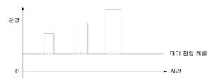
일 실시예에서, 상기 전기장을 인가하기 전에 상기 입자의 간격, 위치 또는 배열을 사전 설정된 간격, 위치 또는 배열로 유지하기 위하여 대기(standby) 전기장을 인가한다.In one embodiment, a standby electric field is applied to maintain the spacing, position or arrangement of the particles at a predetermined spacing, position or arrangement prior to applying the electric field.
일 실시예에서, 상기 표시부에 커패시터가 접속되어서 전압이 인가되면 상기 커패시터에 전하가 충전되도록 하고 상기 표시부에 인가되는 전압이 차단되면 상기 커패시터에 충전된 전하를 이용하여 상기 표시부에 전압을 인가한다.In one embodiment, a capacitor is connected to the display unit to charge the capacitor when a voltage is applied, and when the voltage applied to the display unit is cut off, a voltage is applied to the display unit by using the charge charged in the capacitor.
일 실시예에서, 표시 면적, 표시 시간 및 광 투과도 중 적어도 하나를 조절함으로써 표시되는 컬러의 명도 또는 채도를 제어한다.In one embodiment, the brightness or saturation of the displayed color is controlled by adjusting at least one of display area, display time and light transmittance.
일 실시예에서, 서로 다른 부호의 전하를 갖는 제 1 및 제 2 입자에 전기장을 인가하여 상기 제 1 입자의 간격, 위치 또는 배열과 상기 제 2 입자의 간격, 위치 또는 배열이 서로 독립적으로 제어한다.In one embodiment, an electric field is applied to the first and second particles having different sign charges to control the spacing, position or arrangement of the first particles and the spacing, position or arrangement of the second particles independently of one another. .
일 실시예에서, 상기 입자 및 상기 용매에 입사되는 광을 이용하여 에너지를 발생시키고 상기 발생된 에너지를 이용하여 상기 전기장을 인가한다.In one embodiment, energy is generated using light incident on the particles and the solvent and the electric field is applied using the generated energy.
일 실시예에서, 발광형 표시 수단을 사용하여 상기 모드를 구현하거나 발광형 표시 수단을 상기 모드와 조합하여서 사용한다.In one embodiment, the light emitting display means is used to implement the mode or the light emitting display means is used in combination with the mode.
일 실시예에서, 상기 입자, 상기 용매 또는 상기 전극으로부터 반사되거나 상기 입자, 상기 용매 또는 상기 전극을 투과하는 광이 상기 전극에 결합된 컬러 필터를 통과하여 표시되도록 한다.In one embodiment, the light reflected from the particles, the solvent or the electrode or transmitted through the particles, the solvent or the electrode is displayed through a color filter coupled to the electrode.
일 실시예에서, 상기 입자 및 상기 전극은 각각 흰색 및 검은색이거나 각각 검은색 및 흰색이다.In one embodiment, the particles and the electrode are white and black, respectively, or black and white, respectively.
일 실시예에서, 상기 입자들의 간격을 제어함으로써 반사되는 광의 파장을 조절하는 모드는 상기 입자들의 배열을 제어함으로써 광의 투과도를 조절하는 모드보다 그 인가되는 전압의 크기가 작다.In one embodiment, the mode of adjusting the wavelength of the reflected light by controlling the spacing of the particles is smaller in magnitude than the mode of controlling the transmittance of light by controlling the arrangement of the particles.
일 실시예에서, 인가되는 전압이 커질수록 가변 전기 분극 특성에 의한 입자 간의 인력이 입자 간의 반발력보다 반발력을 무시할 정도로 커지게 된다.In one embodiment, as the applied voltage increases, the attractive force between the particles due to the variable electric polarization characteristic becomes larger so as to ignore the repulsive force than the repulsive force between the particles.
일 실시예에서, 상기 입자들의 배열을 제어함으로써 광의 투과도를 조절하는 모드에서는 상기 가변 전기 분극 특성에 의한 입자 간의 인력이 입자 간의 반발력보다 크도록 된다.In one embodiment, in the mode of adjusting the transmittance of light by controlling the arrangement of the particles, the attractive force between the particles due to the variable electrical polarization property is greater than the repulsive force between the particles.
일 실시예에서, 상기 투과도를 조절하는 모드에서, 투과도는 연속적으로 변화하는 것을 특징으로 한다.
In one embodiment, in the mode of adjusting the transmittance, the transmittance is characterized in that it continuously changes.
본 발명에 따르면, 다양한 색상 또는 연속적인 색상 및/또는 투과도가 동일한 단일 화소 내에서 간단한 구조로 해서 구현될 수 있다.According to the present invention, it can be implemented as a simple structure in a single pixel in a variety of colors or continuous colors and / or the same transmittance.
본 발명에 따르면, 다양한 색상, 투과도, 채도 및/또는 명도가 간단한 구조로 해서 조절될 수 있다.According to the present invention, various hue, transmittance, saturation and / or brightness can be adjusted with a simple structure.
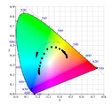
본 발명에 따르면, R,G,B의 혼색에 의한 색상(hue) 구현이 아니라 연속적인 파장의 광을 반사시킴으로써 연속적인 파장의 색상을 구현할 수 있다.According to the present invention, the color of the continuous wavelength can be realized by reflecting the light of the continuous wavelength rather than the color (hue) by the mixed color of R, G, and B.
본 발명에 따른 표시 방법은 대형 면적 표시, 간단한 표시 방법, 연속적인 색상 구현, 플렉시블한 표시 영역에서의 사용, 저 전력 소비의 표시를 동시에 충족시킬 수 있다.The display method according to the present invention can simultaneously satisfy large area display, simple display method, continuous color implementation, use in a flexible display area, and display of low power consumption.
본 발명에 따르면, 시야각(viewing angle) 특성 및 반응 속도(response time)가 우수한 표시 방법 및 장치가 제공될 수 있다.
According to the present invention, a display method and an apparatus excellent in viewing angle characteristics and response time can be provided.
본 발명의 상술한 장점, 특징 및 목적과 또 다른 장점, 특징 및 목적은 다음의 발명의 상세한 설명을 다음의 첨부 도면을 참조하여 독해하면 명백해질 것이다.
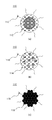
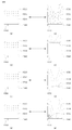
도 1 및 도 2는 본 발명의 일 실시예에 따른 표시 장치에 포함되는 입자의 구성을 예시적으로 나타내는 도면이다.
도 3은 본 발명의 일 실시예에 따라 전기장이 인가됨에 따라 입자 또는 용매가 분극되는 구성을 예시적으로 나타내는 도면이다.
도 4는 본 발명의 일 실시예에 따라 분자의 비대칭적 배치에 의한 단위 분극 특성을 예시적으로 나타내는 도면이다.
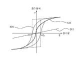
도 5는 상유전체, 강유전체 및 초상유전체의 이력 곡선을 나타내는 도면이다.
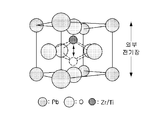
도 6은 본 발명의 일 실시예에 따른 입자 또는 용매에 포함될 수 있는 페로브스카이트 구조를 갖는 물질을 예시적으로 나타내는 도면이다.
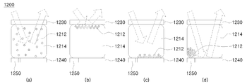
도 7은 본 발명에 따른 표시 장치의 제 1 모드의 제 1 실시예에 따라 입자의 간격을 제어하는 구성을 개념적으로 나타내는 도면이다.
도 8은 본 발명에 따른 표시 장치의 제 1 모드의 제 2 실시예에 따라 입자의 간격을 제어하는 구성을 개념적으로 나타내는 도면이다.
도 9 및 도 10은 본 발명의 일 실시예에 따른 표시 장치의 제 1 모드의 제 1 및 제 2 실시예에 따른 표시 장치의 구성을 각각 개념적으로 나타내는 도면이다.
도 11은 본 발명의 일 실시예에 따라 제 1 모드의 구성을 예시적으로 나타내는 도면이다.
도 12는 본 발명의 일 실시예에 따른 표시 장치의 제 2 모드의 구성을 예시적으로 나타내는 도면이다.
도 13은 본 발명의 일 실시예에 따른 표시 장치의 제 2 모드의 구성을 예시적으로 나타내는 도면이다.
도 14는 본 발명의 일 실시예에 따른 표시 장치의 제 3 모드의 구성을 예시적으로 나타내는 도면이다.
도 15는 본 발명의 일 실시예에 따라 제 1 및 제 2 모드를 선택적으로 수행할 수 있는 표시 장치의 구성을 예시적으로 나타내는 도면이다.
도 16은 본 발명의 일 실시예에 따라 제 1 및 제 3 모드를 선택적으로 수행할 수 있는 표시 장치의 구성을 예시적으로 나타내는 도면이다.
도 17은 본 발명의 일 실시예에 따라 제 2 및 제 3 모드를 선택적으로 수행할 수 있는 표시 장치의 구성을 예시적으로 나타내는 도면이다.
도 18은 본 발명의 일 실시예에 따라 제 1, 제 2 및 제 3 모드를 선택적으로 수행할 수 있는 표시 장치의 구성을 예시적으로 나타내는 도면이다.
도 19는 본 발명의 일 실시예에 따라 복수의 전극에 의하여 구동되는 표시 장치의 구성을 예시적으로 나타내는 도면이다.
도 20은 본 발명의 일 실시예에 따라 표시 장치에 포함되는 입자 및 용매를 복수의 캡슐로 캡슐화하는 구성을 예시적으로 나타내는 도면이다.
도 21은 본 발명의 일 실시예에 따라 표시 장치에 포함되는 입자 및 용매를 매질 내에 산재시키는 구성을 예시적으로 나타내는 도면이다.
도 22는 본 발명의 일 실시예에 따라 광투광성 매질로 캡슐화된 용액의 구성을 예시적으로 나타내는 도면이다.
도 23은 본 발명의 일 실시예에 따라 매질 내에 산재된 입자 및 용매의 구성을 예시적으로 나타내는 도면이다.
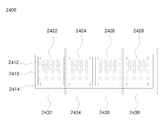
도 24는 본 발명의 일 실시예에 따라 표시 장치에 포함되는 입자 및 용매를 복수의 셀로 구획화하는 구성을 예시적으로 나타내는 도면이다.
도 25 및 도 26은 본 발명의 일 실시예에 따라 표시 장치가 서로 수직 방향 또는 수평 방향으로 결합되는 구성을 예시적으로 나타내는 도면이다.
도 27 내지 도 29는 본 발명의 일 실시예에 따라 표시 장치에 인가되는 전압의 패턴을 예시적으로 나타내는 도면이다.
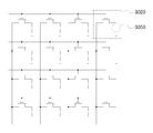
도 30은 본 발명의 일 실시예에 따라 표시 장치의 복수의 전극에 연결되는 회로 구성을 예시적으로 나타내는 도면이다.
도 31은 본 발명의 일 실시예에 따라 입자로부터 반사되는 광의 표시 면적을 조절하는 구성을 예시적으로 나타내는 도면이다.
도 32는 본 발명의 일 실시예에 따라 입자로부터 반사되는 광의 표시 시간을 조절하는 구성을 예시적으로 나타내는 도면이다.
도 33은 본 발명의 일 실시예에 따라 광 조절층을 이용하여 명도를 조절하는 구성을 예시적으로 나타내는 도면이다.
도 34 및 도 35는 본 발명의 일 실시예에 따라 광 투과도를 조절하는 광 조절층의 구성을 예시적으로 나타내는 도면이다.
도 36은 본 발명의 일 실시예에 따라 광 차단율을 조절하는 광 조절층의 구성을 예시적으로 나타내는 도면이다.
도 37은 본 발명의 일 실시예에 따라 서로 다른 전하를 갖는 입자를 이용하여 광결정성 디스플레이를 구현하는 표시 장치의 구성을 예시적으로 나타내는 도면이다.
도 38 내지 도 40은 본 발명의 일 실시예에 따라 전극을 이루는 전극을 패터닝하는 구성을 예시적으로 나타내는 도면이다.
도 41은 본 발명의 일 실시예에 따른 표시 장치가 스페이서를 포함하는 구성을 예시적으로 나타내는 도면이다.
도 42는 본 발명의 일 실시예에 따라 태양 전지부를 포함하는 표시 장치의 구성을 예시적으로 나타내는 도면이다.
도 43은 본 발명에 따른 표시 장치를 발광형 표시 장치와 결합한 구성을 예시적으로 나타내는 도면이다.
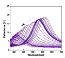
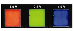
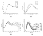
도 44 내지 도 46은 본 발명의 일 실시예에 따라 전하를 갖는 입자를 전기 분극 특성을 갖는 용매에 분산시킨 상태에서 전기장을 인가하여 입자의 간격을 조절함으로써 입자로 이루어진 광결정으로부터 반사되는 광의 파장을 제어하는 제 1 모드를 구현한 실험 결과를 그래프 및 사진으로 나타내는 도면이다.
도 47 및 도 48은 본 발명의 일 실시예에 따라 전하를 갖는 입자를 서로 다른 극성 지수를 갖는 다양한 용매에 분산시킨 상태에서 전기장을 인가하여 제 1 모드를 구현하는 실험을 수행한 결과 입자로부터 반사되는 광의 파장을 그래프로서 나타내는 도면이다.
도 49 및 도 50은 본 발명의 일 실시예에 따라 전하를 갖고 전기 분극 특성을 갖는 입자를 용매에 분산시킨 상태에서 전기장을 인가하여 제 1 모드를 구현하는 실험을 수행한 결과 입자로부터 반사되는 광을 그래프 및 사진으로서 나타내는 도면이다.
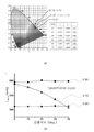
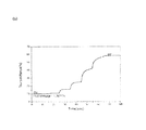
도 51은 본 발명의 일 실시예에 따른 표시 장치의 관찰각에 대한 의존도(즉, 표시 장치의 시야각)에 대한 실험을 수행한 결과를 나타내는 도면이다.
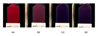
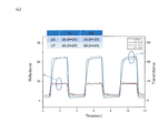
도 52는 본 발명의 일 실시예에 따라 제 1 및 제 2 모드 중 어느 하나의 모드를 전환 가능하게 선택적으로 수행하는 표시 장치에 대한 실험 결과를 나타내는 도면이다.
도 53 및 도 54는 본 발명의 일 실시예에 따라 제 1 및 제 3 모드 중 어느 하나의 모드를 전환 가능하게 선택적으로 수행하는 표시 장치에 대한 실험 결과를 나타내는 도면이다.
도 55 및 도 56은 본 발명의 일 실시예에 따라 제 2 및 제 3 모드 중 어느 하나의 모드를 전환 가능하게 선택적으로 수행하는 표시 장치에 대한 실험 결과를 나타내는 도면이다.
도 57은 제 2 모드 간에서의 모드 전환 구성의 일 실시예를 나타내고 있다.
도 58은 제 3 모드 간에서의 모드 전환 구성의 일 실시예를 나타내고 있다.
도 59는 모드 구현 및 모든 전환 구현을 위한 파장, 인가 전압 및 반사도 간의 관계를 나타내는 그래프이다.
[발명의 실시를 위한 구체적인 내용]
후술하는 본 발명에 대한 상세한 설명은, 본 발명이 실시될 수 있는 특정 실시예를 예시로서 도시하는 첨부 도면을 참조한다. 이들 실시예는 당업자가 본 발명을 실시할 수 있기에 충분하도록 상세히 설명된다. 본 발명의 다양한 실시예는 서로 다르지만 상호 배타적일 필요는 없음이 이해되어야 한다. 예를 들어, 여기에 기재되어 있는 특정 형상, 구조 및 특성은 일 실시예에 관련하여 본 발명의 정신 및 범위를 벗어나지 않으면서 다른 실시예로 구현될 수 있다. 또한, 각각의 개시된 실시예 내의 개별 구성요소의 위치 또는 배치는 본 발명의 정신 및 범위를 벗어나지 않으면서 변경될 수 있음이 이해되어야 한다. 본 명세서 전반에 걸쳐서 사용되는 표현 "일 실시예에 따라서" 또는 "일 실시예에서"가 등장하면, 이는 특정 일 실시예에서 기술된 형상, 구조, 특성, 방식, 구성 등이 반드시 모든 실시예들에서도 동일하게 적용됨을 의미하지 않으며, 또한 특정 실시예에서 기술된 형상, 구조, 특성, 방식, 구성 등이 이 특정 실시예에서만 적용되는 것도 의미하지 않는다. 또한, 특정 실시예들에서 사용되는 형상, 구조, 특징부, 특성, 구성 등은 다른 실시예들과 서로 결합될 수 있다.
또한, 본 명세서의 사용되는 명사의 단수형은 복수형의 존재를 배제하지 않는다. 또한, 본 명세서에서 사용되는 용어 "포함한다" 및 "갖는다" 및 "구비한다" 및 이의 활용어는 기술된 구성 요소 또는 단계 이외의 구성 요소 또는 단계의 존재를 배제하지 않는다. 또한, 본 명세서에서 사용되는 프로세스의 단계들의 순서들은 본 명세서에서 기술된 바대로만 한정되는 것이 아니라 다른 순서도 가능하다. 본 명세서에서 사용되는 서수인 "제 1, 제 2, 제 3" 등은 구성 요소 또는 모드 또는 단계를 서로 간에 구별할 뿐이지 어떠한 순서상의 의미도 부여하지 않으며, 또한 특정 모드는 제 1 모드, 제 2 모드 또는 제 3 모드로도 지칭될 있다. 가령, 본 명세서에서, 제 1 모드는 광 결정 반사 모드를 나타내지만 청구 범위에서는 제 1 모드는 광 결정 반사 모드 이외의 다른 모드가 될 수 있다. 또한, 본 명세서에서 제 2 모드는 고유색 반사 모드를 나타낼 수 있지만 청구 범위에서는 고유색 반사 모드 이외의 다른 모드가 될 수 있다. 이는 또한 제 3 모드에 대해서도 적용된다. 즉, 본 발명을 체계적으로 설명하기 위해서, 제 1 모드를 광 결정 반사 모드, 제 2 모드를 고유색 반사 모드, 제 3 모드를 투과도 조절 모드로 해서 본 명세서에서 각 모드를 설명하고 있지만 본 발명은 이러한 설명 방식에만 한정되지 않는다.
따라서, 후술하는 상세한 설명은 한정적인 의미로서 취하려는 것이 아니며, 본 발명의 범위는, 적절하게 설명된다면, 그 청구항들이 주장하는 것과 균등한 모든 범위와 더불어 첨부된 청구항에 의해서만 한정된다. 도면에서 유사한 참조부호는 여러 측면에 걸쳐서 동일하거나 유사한 기능을 지칭한다.
이하, 본 발명이 속하는 기술분야에서 통상의 지식을 가진 자가 본 발명을 용이하게 실시할 수 있도록 하기 위하여, 첨부된 도면을 참조하여 본 발명의 구성을 상세하게 설명하도록 한다.
표시 장치의 구성
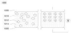
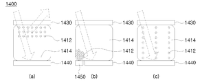
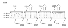
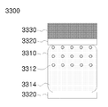
본 발명의 일 실시예에 따른 표시 장치는 복수의 입자가 용매 내에 분산된 상태에서 전극을 통하여 전기장을 인가하고 전기장의 세기, 방향, 인가시간, 인가횟수, 인가영역 중 적어도 하나를 조절하여 입자의 간격, 위치 및 배열 중 적어도 하나를 제어함으로써, 입자로 구성되는 광결정으로부터 반사되는 광의 컬러를 표시하는 제 1 모드(광 결정 반사 모드), 입자, 용매, 전극 등의 고유의 컬러 또는 입자의 산란에 의한 용액의 컬러를 표시하는 제 2 모드(고유색 반사 모드) 및 투과도가 제어된 광의 컬러를 표시하는(즉, 광의 투과도를 제어하는) 제 3 모드(투과도 조절 모드) 중 적어도 2 개의 모드를 표시 장치의 표시 영역 또는 표시부의 동일한 단일 화소(unit pixel) 내에서 서로 전환 가능하게 선택적으로 구현할 수 있다. 이하의 설명에서도 알 수 있는 바와 같이, 단일 화소는 독립적으로 제어될 수 있는 최소의 표시 단위를 말한다. 즉, 기존의 디스플레이 방식에서는 적색의 셀, 녹색의 셀, 청색의 셀이 하나의 단일 화소를 형성할 수 있지만 이는 R,G,B 컬러의 혼색에 의해서 색상을 구현하는 방식에서의 가령 3 개의 셀이 하나의 단일 화소를 형성하지만, 본 기술에서는 하나의 단일 셀 또는 단일 화소가 독립적으로 제어되어서 연속적인 색상을 구현할 수 있으므로 본 명세서에서 단일 화소란 기존의 방식과는 달리 독립적으로 제어될 수 있는 최소의 표시 단위 또는 표시 영역 또는 표시부를 의미하는 것이 주목될 필요가 있다.
입자 및 용매의 구성
도 1 및 도 2는 본 발명의 일 실시예에 따른 표시 장치에 포함되는 입자의 구성을 예시적으로 나타내는 도면이다.
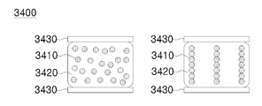
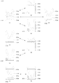
먼저, 도 1을 참조하면, 본 발명의 일 실시예에 따른 입자(110)는 용매(120)에 분산되어 용액 상태로 존재할 수 있다. 본 발명의 일 실시예에 따르면, 입자(110)는 양전하 또는 음전하를 가질 수 있다. 따라서, 입자(110)에 전기장이 인가되는 경우에 입자(110)가 갖는 전하와 전기장에 의해 발생하는 전기적 인력으로 인하여 입자(110)가 이동(즉, 전기 영동)될 수 있다. 또한, 복수의 입자(110)가 동일한 부호의 전하를 갖는 경우에는 동일한 부호의 전하로 인한 상호간의 전기적 척력(쿨롱 반발력)으로 인하여 복수의 입자(110)가 서로 접촉하지 않고 소정의 간격을 유지한 채로 배열되어 있을 수 있다. 또한, 본 발명의 일 실시예에 따르면 입자(110)는 고분자 사슬 형태 등으로 코팅되어 입자 간 고분자 사슬의 무질서한 운동 등에 의한 입체장애 효과(steric effect)가 존재할 수 있다. 따라서, 입자간 입체장애 효과에 인하여 복수의 입자(110)가 서로 접촉하지 않고 소정의 간격을 유지한 채로 배열되어 있을 수 있다.
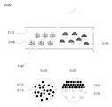
도 2를 참조하면, 본 발명의 일 실시예에 따른 입자(110)는, 도 2의 (a)와 같이 이종의 물질로 이루어진 코어-셀(core-shell)(112) 형태로 구성될 수 있고, 도 2 (b)와 같이 이종의 물질로 이루어진 멀티-코어(multi-core)(114) 형태로 구성될 수 있고, 도 2의 (c)와 같이 복수의 나노 입자로 이루어진 클러스터(116)로 구성될 수 있으며, 상기 기술한 전하를 갖는 전하층(118) 또는 입체장애 효과(steric effect)를 나타내는 층(118)이 이들 입자를 감싸는 구조로 구성될 수 있다. 본 발명에 의한 입자는 상기 구조에 국한되지 않으며, 코아 입자에 이종 물질을 침투 혹은 담지 시킨 구조, 라즈베리(raspberry) 구조 등과 같이 다양한 입자 및 형태를 이용할 수 있으며, 역광결정 구조와 같이 공공(cavity) 구조 도 사용할 수 있다.
보다 구체적으로, 본 발명의 일 실시예에 따른 입자(110)는 실리콘(Si), 티타늄(Ti), 바륨(Ba), 스트론튬(Sr), 철(Fe), 니켈(Ni), 코발트(Co), 납(Pb), 알루미늄(Al), 구리(Cu), 은(Ag), 금(Au), 텅스텐(W), 몰리부덴(Mo), 아연(Zn), 지르코늄(Zr) 등의 원소나 이들을 포함하는 산화물, 질화물 등의 화합물로 이루어질 수 있다. 또한, 본 발명의 일 실시예에 따른 입자(110)는 styrene, pyridine, pyrrole, aniline, pyrrolidone, acrylate, urethane, thiophene, carbazole, fluorene, vinylalcohol, ethylene glycol, ethoxy acrylate 중 적어도 하나의 단위체를 포함하는 유기 고분자 또는 PS(polystyrene), PE(polyethylene), PP(polypropylene), PVC(polyvinyl chloride), PET(polyethylen terephthalate) 등의 고분자 물질로 이루어질 수 있다.
또한, 본 발명의 일 실시예에 따른 입자(110)는 전하를 갖지 않는 입자 혹은 클러스터(cluster)에 전하를 갖는 물질이 코팅된 형태로서 구성될 수도 있다. 예를 들면, 탄화수소기를 갖는 유기화합물에 의하여 표면이 가공(혹은 코팅)된 입자, 카르복실산(carboxylic acid)기, 에스테르(ester)기, 아실(acyl)기를 가지는 유기 화합물에 의하여 표면이 가공(혹은 코팅)된 입자, 할로겐(F, Cl, Br, I 등) 원소를 포함하는 착화합물에 의하여 표면이 가공(코팅)된 입자, 아민(amine), 티올(thiol), 포스핀(phosphine)을 포함하는 배위화합물에 의하여 표면이 가공(코팅)된 입자, 표면에 라디칼을 형성함으로써 전하를 갖는 입자가 이에 해당될 수 있다. 이와 같이 입자(110)의 표면을 실리카, 고분자, 고분자 단량체 등의 물질로 코팅함으로써 입자(110)가 용매(120) 내에서 높은 분산성과 안정성을 갖도록 할 수 있다.
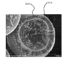
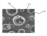
한편, 입자(110)의 직경은 수 nm 내지 수백 μm일 수 있으나, 반드시 이에 한정되는 것은 아니며, 외부 전기장에 의해 입자 들이 일정한 거리로 배열될 때 브래그 법칙(Bragg의 Law)에 의해 입자의 굴절률 및 용매의 굴절률과 연계되어 가시광 영역의 광결정 파장대가 포함될 수 있는 입자의 크기로 설정할 수 있다.
한편, 본 발명의 일 실시예에 따르면, 입자(110)는 특정 파장의 광을 반사시킬 수 있도록, 즉 고유의 컬러를 갖도록 구성될 수 있다. 보다 구체적으로, 본 발명의 일 실시예에 따른 입자(110)는 산화수 조절 또는 무기 안료, 안료 등의 코팅을 통하여 특정 컬러를 갖게 될 수 있다. 예를 들면, 본 발명에 따른 입자(110)에 코팅되는 무기 안료로는 발색단을 포함하는 Zn, Pb, Ti, Cd, Fe, As, Co, Mg, Al 등이 산화물, 유화물, 유산염의 형태로 사용될 수 있고, 본 발명에 따른 입자(110)에 코팅되는 염료로는 형광 염료, 산성 염료, 염기성 염료, 매염 염료, 황화 염료, 배트 염료, 분산 염료, 반응성 염료 등이 사용될 수 있다. 또한, 본 발명의 일 실시예에 따르면, 입자(110)는 특정 컬러를 표시할 수 있도록 특정 구조색(structural color)을 갖는 물질일 수도 있다. 예를 들면, 실리콘 산화물(SiOx), 티타늄산화물(TiOx) 등의 입자가 굴절률이 다른 매체에 일정한 간격으로 균일하게 배열된 형태로 구성되어 특정 파장의 광을 반사시키는 물질일 수 있다.
또한, 본 발명의 일 실시예에 따르면, 용매(120) 역시 특정 파장의 광을 반사시킬 수 있도록, 즉 고유의 컬러를 갖도록 구성될 수 있다. 보다 구체적으로, 본 발명에 따른 용매(120)는 무기 안료, 염료를 갖는 물질을 포함하거나 광결정에 의한 구조색을 갖는 물질을 포함할 수 있다.
또한, 본 발명의 일 실시예에 따르면 상기 입자 또는 용매에 형광물질, 인광물질, 발광물질 등이 적어도 하나 포함되어 본 발명의 효과를 극대화 시킬 수 있다.
본 발명의 일 실시예에 따르면, 용매(120)는 입자(110)가 용매(120) 내에 균일하게 분산되어 콜로이달 안정성을 확보하기 위해서, 입자(110)가 용매(120) 내에서 안정적으로 분산 되도록 분산제 등의 첨가제를 용매에 첨가하거나, 입자(110)와 용매(120)의 비중 차이가 기설정된 값 이하일 수 있으며, 용매(120)의 점도가 기 설정된 값 이상 일 수 있으며, 입자(110)와 용매(120)로 이루어진 콜로이드 용액의 계면동전위(electrokinetic potential)(즉, 제타 전위)의 값이 기설정된 값 이상으로 높을 수 있다.
또한, 본 발명의 일 실시예에 따르면, 전기장 인가시 입자(110)가 용매(120) 내에서 소정의 배열을 통해 발생되는 가시광 영역의 반사광 세기를 크게 하기 위하여, 용매(120)와 입자(110)의 굴절률 차이가 기설정된 값 이상일 수 있으며, 입자(110)의 크기는 브래그 법칙(Bragg의 Law)에 의해 입자의 굴절률 및 용매의 굴절률과 연계되어 가시광 영역의 광결정 파장대가 포함될 수 있는 입자의 크기로 설정할 수 있다.
예를 들면, 콜로이드 용액의 계면동전위의 절대값은 10mV 이상일 수 있고, 입자(110)와 용매(120)의 비중 차이는 5 이하일 수 있으며, 입자(110)와 용매(120)의 굴절률 차이는 0.3 이상일 수 있으며, 입자크기는 100nm~500nm 사이일 수 있으나 이에 국한하지는 않는다.
입자간 인력: 전기 분극 특성
또한, 본 발명의 일 실시예에 따르면, 표시 장치에 포함되는 입자가 분산된 용매를 포함하는 용액은 가변 전기 분극(variable electrical polarization) 특성-전기장이 인가되면 전기 분극량이 변화함-을 가질 수 있는데, 이러한 용액의 전기 분극 특성은 용액을 구성하고 있는 입자 또는 용매 중 적어도 하나가 전기 분극 특성을 나타내거나 용액 내에서 입자와 용매의 상호작용에 의해 전기 분극 특성이 나타날 수 있다. 또한 전기 분극 특성을 나타내는 용액(입자 및 용매로 구성)은 원자 혹은 분자의 비대칭적인 전하 분포 등으로 인하여 외부 전기장이 인가됨에 따라 전자 분극, 이온 분극, 계면 분극 및 회전 분극 중 어느 하나에 의하여 전기 분극되는 물질을 포함할 수 있다.
따라서, 본 발명의 일 실시예에 따른 입자 또는 용매 또는 이들로 구성된 용액 중 적어도 하나는 전기장이 인가되면 전기 분극이 유발될 수 있으며, 인가되는 전기장의 세기 또는 방향이 변함에 따라 상기 유발된 전기 분극량이 변할 수 있다. 이렇게 전기장이 변함에 따라 전기 분극량이 변하는 특성을 가변 전기 분극 특성이라고 할 수 있을 것이다. 본 발명에 있어 전기장이 인가되었을 때에 유발되는 전기 분극량이 크면 클수록 유리한데, 그 이유는 전기장을 인가함에 따라서 입자, 용매, 용액 중의 적어도 하나의 전기분극에 의해 입자 간의 상호작용힘이 더 크게 작용하여 입자간의 간격을 더 균일하게 배열할 수 있기 때문이다.
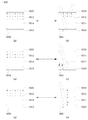
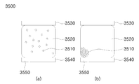
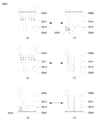
도 3은 본 발명의 일 실시예에 따라 전기장이 인가됨에 따라 입자 또는 용매가 분극되는 구성을 예시적으로 나타내는 도면이다.
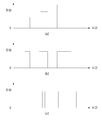
도 3의 (a) 및 (b)를 참조하면, 외부 전기장이 인가되지 않는 경우에 입자 또는 용매가 전기적 평형 상태를 유지하여 전기 분극 특성을 나타내지 않지만, 외부 전기장이 인가되는 경우에는 입자 또는 용매 내의 전하가 소정 방향으로 이동함에 따라 분극이 유발되어 입자 또는 용매가 분극될 수 있다. 도 3의 (c) 및 (d)는 입자 또는 용매를 구성하는 전기적으로 비대칭적인 구성요소에 의하여 단위 분극(unit polarization)이 생성되는 경우로서, 전기장을 인가하지 않은 경우에는 상기 단위 분극이 무질서하게 배열되어 전체 전기 분극은 나타나지 않거나 작은 값을 나타내지만, 외부에서 전기장이 인가되는 경우에는 단위 분극을 갖는 입자 또는 용매가 외부 전기장의 방향에 따라 소정의 방향으로 재배열될 수 있어 전체적으로 단위 분극이 없는 상태에서 전기장을 인가하는 도 3의 (b)의 경우에 비해 상대적으로 큰 전기 분극값(polarization value)을 나타낼 수 있다. 본 발명의 일 실시예에 따르면, 도 3 (c) 및 (d)에 표시된 단위 분극은 전자 또는 이온의 비대칭적 배치나 분자의 비대칭적 구조에서 발생할 수 있으며, 이러한 단위 분극으로 인하여 외부 전기장이 인가되지 않는 경우에도 미세한 잔류 분극값(remnant polarization value)이 나타날 수 있다.
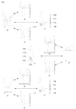
도 4는 본 발명의 일 실시예에 따라 분자의 비대칭적 배치에 의한 단위 분극 특성을 예시적으로 나타내는 도면이다. 보다 구체적으로, 도 4는 물 분자(H2O)의 경우를 예시적으로 나타낸 것으로, 물 분자 외에 Trichloroethylene, Carbon Tetrachloride, Di-Iso-Propyl Ether, Toluene, Methyl-t-Bytyl Ether, Xylene, Benzene, DiEthyl Ether, Dichloromethane, 1,2-Dichloroethane, Butyl Acetate, Iso-Propanol, n-Butanol, Tetrahydrofuran, n-Propanol, Chloroform, Ethyl Acetate, 2-Butanone, Dioxane, Acetone, Metanol, Ethanol, Acetonitrile, Acetic Acid, Dimethylformamide, Dimethyl Sulfoxide, Propylene carbonate, N,N-Dimethylformamide, Dimethyl Acetamide, N-Methylpyrrolodone 등은 분자 구조의 비대칭성에 의해 단위 분극 특성이 나타낼 수 있으므로 본 발명에 따른 입자 또는 용매를 구성하는 물질로서 채용될 수 있을 것이다. 참고로, 물질의 분극 특성을 비교하기 위하여 사용되는 극성 지수(polarity index)는, 물(H2O)의 분극 특성에 대비하여 해당 물질의 상대적인 분극 정도를 나타내는 지표일 수 있으며, 본 발명의 일 실시예에 따르면 용매는 극성 지수(polarity index)가 1 이상인 물질을 포함할 수 있다.
또한, 본 발명의 일 실시예에 따른 입자 또는 용매는, 외부 전기장이 인가됨에 따라 이온 또는 원자의 전기분극이 추가 유발되어 분극량이 크게 증가하고, 외부 전기장이 인가되지 않는 경우에도 잔류 분극량이 존재하며 전기장 인가 방향에 따라 이력(hysteresis)이 남는 강유전성(ferroelectric) 물질을 포함할 수 있고, 외부 전기장이 인가됨에 따라 이온 또는 원자 분극이 추가 유발되어 분극량이 크게 증가하지만, 외부 전기장이 인가되지 않는 경우에는 잔류 분극량과 이력(hysteresis)이 남지 않는 초상유전성(superparaelectric) 물질을 포함할 수 있다. 도 5를 참조하면, 상유전성 물질(510), 강유전성 물질(520) 및 초상유전성 물질(530)의 외부 전기장에 따른 이력 곡선을 확인할 수 있다.
또한, 본 발명의 일 실시예에 따른 입자 또는 용매는 페로브스카이트(perovskite) 구조를 갖는 물질을 포함할 수 있는데, ABO3와 같은 페로브스카이트 구조를 갖는 물질로서 PbZrO3, PbTiO3, Pb(Zr,Ti)O3, SrTiO3 BaTiO3, (Ba, Sr)TiO3, CaTiO3, LiNbO3 등의 물질을 그 예로 들 수 있다.
도 6은 본 발명의 일 실시예에 따른 입자 또는 용매에 포함될 수 있는 페로브스카이트 구조를 갖는 물질을 예시적으로 나타내는 도면이다. 도 6을 참조하면, PbZrO3(또는 PbTiO3)에 인가되는 외부 전기장의 방향에 따라 PbZrO3(또는 PbTiO3) 내에서의 Zr(또는 Ti)(즉, ABO3 구조에서의 B)의 위치가 변동될 수 있으며 이로 인하여 PbZrO3(또는 PbTiO3) 전체의 극성이 바뀔 수 있게 된다. 따라서, 원자 혹은 이온의 이동에 의해 비대칭적 전자분포가 형성되어 단위 분극(Unit polarization)이 형성될 수 있고, 이러한 단위 분극이 존재하게 되면 전자 분극만 있는 경우에 비해 외부 전기장 인가시 더 큰 가변 전기분극값을 유발시킬 수 있다.
또한, 본 발명의 일 실시예에 의하면 본 발명의 반사광 조절 및 투과도 조절 효과는 입자간 배열이 잘 될수록 극대화 될 수 있기 때문에, 미세입자가 부도체 유체에 분산되어 전기유변(ER: Electro-Rheology) 특성을 나타내는 유체 또는 더 나아가 부도체가 코팅된 강유전체 입자와 같이 극대전기유변(GER:Giant Electro-Rheology) 나타내는 유체를 이용함으로써 본 발명의 효과를 극대화할 수 있다.
또한, 전기 분극의 양상을 말하자면, 제 1 실례로서 전기장이 인가되지 않으면, 상기 용매의 각 분자 및 각 입자 중 적어도 하나는 어떠한 전기 분극량도 가지지 않지만, 전기장이 인가되면 상기 용매의 각 분자 및 각 입자 중 적어도 하나는 전기적으로 분극 되며, 이로써 상기 복수의 입자의 총 전기 분극량 및 상기 용매의 총 전기 분극량 중 적어도 하나는 증가하게 될 수 있다. 제 2 실례에서는, 전기장이 인가되지 않아도, 상기 용매의 각 분자 및 각 입자 중 적어도 하나는 전기적으로 분극 되어 있지만 상기 용매의 총 전기 분극량 및 상기 복수의 입자의 총 전기 분극량 중 적어도 하나는 제로가 되며, 전기장이 인가되면, 상기 복수의 입자의 총 전기 분극량 및 상기 용매의 총 전기 분극량 중 적어도 하나는 증가하게 될 수 있다. 제 3 실례로서, 전기장이 인가되지 않아도, 상기 용매의 각 분자 및 각 입자 중 적어도 하나는 전기적으로 분극되어 있어서 상기 용매의 총 전기 분극량 및 상기 복수의 입자의 총 전기 분극량 중 적어도 하나는 제로가 아닌 제 1 값을 가지며, 전기장이 인가되면, 상기 복수의 입자의 총 전기 분극량 및 상기 용매의 총 전기 분극량 중 적어도 하나는 상기 제 1 값보다 큰 제 2 값이 될 수 있다.
입자간 반발력 : 쿨롱효과 또는 입체 장애 효과
본 발명의 일 실시 예에 따르면, 표시 장치에 포함되는 입자 표면은 동일 부호의 전하로 대전되어 입자가 쿨롱 반발력이 형성되거나, 입자 표면에 고분자 사슬구조, 관능기(functional group), 첨가제(surfactant) 등을 이용하여 입체 구조물 등을 형성시켜 입체장애 반발력(steric hindrance repulsion)이 형성될 수 있다.
또한 본 발명의 일 실시예에 따르면 입자간 반발력을 극대화 하기 위하여, 상기 동일한 부호의 전하로 대전되고 입체구조물 형태로 입자를 코팅하여 상기 콜롱 반발력과 입체장애 반발력을 동시에 유발 시킬 수도 있다.
또한, 본 발명의 일 실시예에 따르면, 입자는 전기분극 되는 물질을 포함하고 입자 표면처리를 통해 입자간 입체장애 반발력은 있으나 대전된 전하가 약하여 전기 영동 효과는 최소화하게 구성함으로써, 상기 입자 혹은 용액은 외부 전기장에 따라 전기 분극량이 변화되어 입자 간 국부적 인력(short range attraction)이 효과적으로 발생하고, 입자 표면 처리를 통해 형성된 입체 구조물에 의해 입자 간 국부적으로 입체 장애 반발력(short range steric hindrance repulsion)은 효과적으로 발생되나, 외부 전기장에 의한 장거리 전기 영동 힘(long range electophoretic force)에 의해 대전된 입자가 전극으로 몰리는 현상을 최소화할 수 있다. 즉, 입자 표면에 전하가 처리되지 않아서 외부 전기장에 의해서 어느 한 전극 쪽으로 전기 영동하는 현상이 최소화될 수 있다. 이렇게 입체 장애 반발력을 주기 위해서 유기 리간드(organic ligand)를 입자 표면에 처리할 수 있다. 또한, 본 발명의 일 실시예에 따르면 대전된 입자를 사용시 상기 전기 영동에 의해 대전된 입자가 전극으로 몰리는 현상을 방지하기 위해, 직류전압이 아닌 교류전압을 조합하여 사용할 수도 있다.
다만, 본 발명에 따른 입자 및 용매의 구성이 반드시 상기 열거한 것에 한정되는 것은 아니며, 본 발명의 목적을 달성할 수 있는 범위 내에서, 즉 전기장에 의하여 입자의 간격이 제어될 수 있는 범위 내에서 적절히 변경될 수 있음을 밝혀 둔다.
가령, 본 발명의 효과를 극대화하기 위해선, 입자와 입자가 분산된 용액의 굴절률 차이를 크게 하여, 전압을 인가하지 않은 경우에는 난반사(산란)를 극대화 시켜 불투명도를 높이고, 전압을 인가하여 구조색을 발현시킬 때에는 구조색의 반사도(reflectance)를 크게 할 수 있다. 일반적으로 유체의 굴절률은 종류에 따라 큰 차이가 없기 때문에, 입자의 굴절률을 극대화하는 방법이 효과적이고, 서로 다른 물질이 두 가지 이상 결합된, 코어/셀(core/shell) 혹은 라즈베리(raspberry) 구조 등으로 제작함으로써 상기 기술한 굴절률 효과와 반발력 효과를 동시에 극대화할 수 있다.
제 1 모드(광 결정 반사 모드)의 동작 원리 및 구성
본 발명의 일 실시예에 따른 표시 장치는, 복수의 입자가 용매 내에 분산된 상태에서 전극을 통하여 전기장을 인가하고 전기장의 세기,방향,인가횟수, 인가시간 중 적어도 하나를 조절하여 입자의 간격을 제어함으로써, 입자구조(즉, 복수의 입자가 소정의 간격을 유지함으로써 형성되는 광결정)로부터 반사되는 광의 컬러가 가변적으로 표시되도록 하는 제 1 모드를 수행할 수 있다. 이하에서는, 본 발명의 일 실시예에 따른 표시 장치의 제 1 모드의 동작 원리 및 구성에 대하여 자세히 설명하기로 한다. 본 명세서 및 청구 범위에서 때때로 제 1 모드는 광 결정 반사 모드(photonic crystal reflection mode)로 지칭될 수 있다. 한편, 본 명세서에서 전반적으로, 반사 모드(광 결정 반사 모드 및 고유색 반사 모드(후술될 것이며 제 2 모드에 대응함))에서도 역시 투과되는 광이 존재할 수 있다. 그러나, 본 발명의 실시예에서, 이러한 반사 모드에서 지배적으로 발생하는 바인 반사되는 광을 사용하기 때문에 투과되는 광의 사용에 대해서는 무시할 수 있다. 또한, 후술할 제 3 모드인 투과도 조절 모드에서 1 차적으로 지배적으로 발생하는 바는 투과되는 광이므로 이 경우 역시 1 차적으로 반사되는 광의 사용에 대해서는 무시하기로 한다. 즉, 본 명세서에서 해당 모드에서 지배적으로(predominantly) 발생하는 광을 사용하는 것이 자명하다. 또한, 상술한 바와 같이, 청구 범위에서는, 제 1 모드는 광 결정 반사 모드가 아닌 다른 모드가 될 수 있으며 이는 단지 체계적 설명을 위한 것일 뿐이므로 본 발명은 이로 한정되어서는 안 된다.
먼저, 본 발명에 따른 표시 장치의 제 1 모드의 일 실시예에 따르면, 동일한 부호의 전하를 갖는 복수의 입자가 전기 분극 특성을 갖는 용매에 분산된 상태에서 입자 및 용매에 전기장이 인가되는 경우, 입자가 갖는 전하로 인하여 복수의 입자에는 전기장의 세기와 입자의 전하량에 비례하는 전기적 힘이 작용하게 되고 이에 따라 복수의 입자는 전기 영동(electrophoresis)되어 소정 방향으로 이동하면서 입자의 간격이 좁아지게 된다. 한편, 이와는 반대로 입자의 간격이 좁아짐에 따라 서로 동일한 부호의 전하를 갖는 복수의 입자 사이에서 발생하는 전기적 척력은 증가하게 되므로 입자의 간격이 계속하여 좁아지지는 않고 소정의 균형을 이루게 되고 이에 따라 복수의 입자는 소정의 간격을 두고 규칙적으로 배열될 수 있게 된다. 또한, 용매가 갖는 전기 분극 특성으로 인하여 전하로 대전된 입자 주위의 용매는 전기분극 되며 서로 영향력을 미치게 되며, 외부 전기장 인가시에는 외부 전기장 방향으로 용매의 전기분극이 배열되며 이로 인해 국부적으로 용매의 전기분극과 상호연계되어 있는 전하로 대전된 입자들도 외부 전기장의 방향으로 배열될 수 있다. 즉, 단위 분극된 용매는 외부에서 인가되는 전기장 및 주변의 입자가 갖는 전하에 의하여 소정의 방향으로 배열되고 이에 따라 입자를 중심으로 하여 국부적으로 형성되는 분극 영역이 형성되어 복수의 입자가 소정의 간격을 유지한 상태로 보다 규칙적이고 안정적으로 배열될 수 있게 된다. 본 발명에 따른 표시 장치의 제 1 모드의 제 1 실시예에 따르면, 외부 전기장으로 인한 전기적 힘(전기 영동력), 서로 동일한 부호의 전하를 갖는 입자 사이의 전기적 힘(쿨롱반발력) 및 분극으로 인한 전기적 힘(쿨롱인력) 등이 평형(equilibrium)을 이루는 거리를 두고 복수의 입자가 규칙적으로 배열될 수 있게 된다. 위와 같은 원리에 따라, 입자의 간격이 소정의 간격으로 제어될 수 있으며, 소정의 간격을 두고 배열된 복수의 입자는 광결정으로서의 기능을 할 수 있게 된다. 규칙적으로 배열된 복수의 입자로부터 반사되는 광의 파장은 입자의 간격에 의해 결정되기 때문에, 외부 전기장의 조절을 통해 입자의 간격을 제어함으로써 복수의 입자로부터 반사되는 광의 파장을 임의로 제어할 수 있게 되는 것이다. 여기서, 반사되는 광의 파장의 패턴은 전기장의 세기 및 방향, 입자의 크기 및 질량, 입자 및 용매의 굴절률, 입자의 전하량, 용매 혹은 입자의 전기 분극 특성, 용매 내의 분산된 입자의 농도 등의 요인에 의하여 다양하게 나타날 수 있다.
도 7은 본 발명에 따른 표시 장치의 제 1 모드의 일 실시예에 따라 입자의 간격을 제어하는 구성을 개념적으로 나타내는 도면이다. 도 7을 참조하면, 외부 전기장이 인가되지 않는 경우에 전하를 갖는 입자(720) 주변의 단위 분극된 용매(710)가 입자의 전하와 상호작용하여 입자 방향으로 강하게 배열되고 입자로부터의 거리가 멀어짐에 따라 단위 분극된 용매(710)가 점차 무질서하게 배열될 수 있다(도 7의 (a) 참조). 또한, 도 7을 참조하면, 외부 전기장이 인가되는 경우에는, 입자(720)가 갖는 전하의 영향력이 미치지 않는 영역(즉, 입자(720)로부터 멀리 떨어진 영역)에 위치하는 단위 분극된 용매(710)가 전기장의 방향으로 재배열되고, 재배열된 용매들의 영향으로 인해 대전된 입자(720)가 재배열 될 수 있다. 즉, 전하로 대전된 입자에 의한 전기적 인력이 강하게 작용하는 영역(즉, 입자(720)와 근접한 영역)에 위치하는 단위 분극된 용매(710)는 입자(720)가 갖는 전하에 의한 전기적 인력으로 인하여 단위 분극의 양극 혹은 음극이 입자(720)를 향하게 되는 방향으로 배열될 수 있고, 이와 같이 입자(720)의 주변 영역의 단위 분극 용매(710)가 입자(720)를 향하는 방향으로 배열되어 있는 영역, 즉, 분극 영역(730)은 마치 전기 분극된 하나의 커다란 입자처럼 작용하여 주변의 다른 분극 영역과 상호작용을 할 수 있으며, 이로써 전하를 갖는 입자(720)가 소정의 간격을 유지한 채 규칙적으로 배열될 수 있게 된다(도 7의 (b) 참조). 도 7은 잔류분극을 가진 용매로 도식하였으나, 잔류분극이 없는 상태에서도 전기장이 인가됨에 따라 전기 분극이 유발되는 특성을 갖는 용매에도 마찬가지로 적용될 수 있다.
다음으로, 본 발명에 따른 표시 장치의 제 1 모드의 일 실시예에 따르면, 동일한 부호의 전하를 갖고 전기 분극 특성을 갖는 복수의 입자가 용매 내에 분산된 상태에서 입자 및 용매에 전기장이 인가되는 경우, 입자가 갖는 전하로 인하여 복수의 입자에는 전기장의 세기와 입자의 전하량에 비례하는 전기적 힘이 작용하게 되고 이에 따라 복수의 입자는 전기 영동(electrophoresis)되어 소정 방향으로 이동하면서 입자의 간격이 좁아지게 된다. 한편, 이와는 반대로 입자의 간격이 좁아짐에 따라 서로 동일한 부호의 전하를 갖는 복수의 입자 사이에서 발생하는 전기적 척력은 증가하게 되므로 입자의 간격이 계속하여 좁아지지는 않고 소정의 균형을 이루게 되고 이에 따라 복수의 입자는 소정의 간격을 두고 규칙적으로 배열될 수 있게 된다. 또한, 전기 분극 특성을 나타내는 입자는 전기장에 의해 분극이 유발되어 전기장의 방향으로 분극되고 이와 같이 분극된 복수의 입자 사이에는 전기적 인력이 국부적으로 발생하게 되어 복수의 입자가 소정의 간격을 유지한 상태로 보다 규칙적이고 안정적으로 배열될 수 있게 된다. 즉, 본 발명에 따른 표시 장치의 상기실시예들에 따르면, 외부 전기장으로 인한 전기적 인력(전기 영동력), 서로 동일한 부호의 전하를 갖는 입자 사이의 전기적 척력(쿨롱반발력) 및 분극으로 인한 전기적 인력(쿨롱인력)이 평형(equilibrium)을 이루는 거리를 두고 복수의 입자가 규칙적으로 배열될 수 있게 된다. 위와 같은 원리에 따라, 입자의 간격이 소정의 간격으로 제어될 수 있으며, 소정의 간격을 두고 배열된 복수의 입자는 광결정으로서의 기능을 할 수 있게 된다. 규칙적으로 배열된 복수의 입자로부터 반사되는 광의 파장은 입자의 간격에 의해 결정되기 때문에, 입자의 간격을 제어함에 따라 복수의 입자로부터 반사되는 광의 파장을 임의로 제어할 수 있게 되는 것이다. 여기서, 반사되는 광의 파장의 패턴은 전기장의 세기 및 방향, 입자의 크기 및 질량, 입자 및 용매의 굴절률, 입자의 전하량, 입자 및 용매의 전기 분극 특성, 용매 내의 분산된 입자의 농도 등의 요인에 의하여 다양하게 나타날 수 있다.
도 8은 본 발명에 따른 표시 장치의 제 1 모드의 일 실시예에 따라 입자의 간격을 제어하는 구성을 개념적으로 나타내는 도면이다. 도 8을 참조하면, 외부 전기장이 인가되지 않는 경우에는 입자(810)가 분극되지 않지만(도 8의 (a) 참조), 외부 전기장이 인가되는 경우에는 입자(810) 내에 포함되어 있는 물질의 전기 분극 특성에 의하여 입자(810)가 분극될 수 있으며 이에 따라 입자(810)가 소정의 간격을 유지한 채 규칙적으로 배열될 수 있게 된다(도 8의 (b) 참조).
본 발명의 상기 실시예들에 있어서, 용매 또는 입자의 전기 분극값이 클수록 분극 영역(730) 또는 분극된 입자(810) 사이의 상호작용의 정도를 증가시킬 수 있으며 이에 따라 입자가 보다 규칙적으로 배열되도록 할 수 있게 된다. 도 8은 잔류분극이 없는 입자로 도식하였으나, 잔류분극이 있는 상태에서도 전기장이 인가됨에 따라 전기 분극이 변화되는 특성을 갖는 입자에도 마찬가지로 적용될 수 있다.한편, 본 발명의 일 실시예에 따른 표시 장치의 제 1 모드의 상기 실시예들에 따른 표시 장치의 구성을 개념적으로 나타내면 각각 도 9 및 도 10과 같다. 본 발명의 일 실시예에 따른 표시 장치의 제 1 모드의 상기 실시예들에 대하여는 이미 도 7 및 도 8을 참조하여 충분히 자세하게 설명하였으므로 도 9 및 도 10에 대한 추가적인 설명은 생략하기로 한다.
이상의 제 1 모드의 실시예에서, 입자 또는 용매가 전기 분극 특성을 갖는 경우에 대하여 설명하였지만 본 발명에 따른 입자 또는 용매가 반드시 전기 분극 특성을 가져야 하는 것은 아님을 밝혀 둔다. 즉, 입자 또는 용매가 전기 분극 특성을 갖지 않는 경우라도 입자가 전하를 갖는다면, 외부 전기장으로 인한 전기적 인력 및 서로 동일한 부호의 전하를 갖는 복수의 입자 사이의 전기적 척력이 평형을 이루는 거리를 두고 복수의 입자가 규칙적으로 배열될 수 있으며, 이와 같이 규칙적으로 배열된 복수의 입자는 임의의 파장의 광을 반사시키는 광결정을 형성할 수 있다.
본 발명의 제 1 모드에서 외부 전기장에 따라 상기 기술한 바와 같이 입자간 작용하는 인력과 척력의 균형에 의해 복수의 입자간 간격이 일정한 간격을 유지할 수 있지만, 상기 인력과 척력이 근거리 입자간에는 효과적으로 작용할 수 있으나 일정거리 이상의 입자간에는 상호작용력이 효과적이지 못할 수도 있기 때문에, 본 발명에 의한 입자들의 배열은 3차원적으로 장거리 배열(Long range ordering)을 하는 것이 아니고 단거리 배열(short range ordering)을 보일 수 있다. 또한 미세하게 서로 다른 배열도를 가지는 단거리 배열들의 집합으로 인해 반사되는 반사광은 기존의 전형적인 광결정 배열에 의해 반사되는 광결정광에 비해 시야각 의존성이 크게 개선된 반사광 특성을 보일 수 있다. 또한, 이상의 제 1 모드의 실시예에서, 입자가 전하를 갖는 경우에 대하여 설명하였지만 본 발명에 따른 입자가 반드시 전하를 가져야 하는 것은 아님을 밝혀 둔다. 즉, 입자가 전하를 갖지 않는 경우라도 입자가 전기 분극 특성을 갖고 입체 장애 반발력을 발생시킬 수 있는 입체 구조물을 갖는다면, 외부 전기장으로 인해 유발된 전기 분극으로 인해 발생하는 인접한 입자 사이의 전기적 인력 및 입체 장애 효과로 인한 척력이 평형을 이루는 거리를 두고 복수의 입자가 규칙적으로 배열될 수 있으며, 이와 같이 규칙적으로 배열된 복수의 입자는 임의의 파장의 광을 반사시키는 광결정을 형성할 수 있다. 다시 말하자면, 복수의 입자들은 상호 입체 장애 효과(steric effect)를 나타내면, 전기장이 인가됨에 따라, 가변 전기 분극 특성에 의해 입자들 간에 작용하는 정전기적 인력과, 입자들 간에 작용하는 입체 장애 반발력이 상호 작용하여 입자 간의 간격이 특정 범위에 도달하게 되고, 상기 입자 간의 간격이 상기 특정 범위에 도달하게 됨에 따라 복수의 입자로부터 특정 파장의 광이 반사되어서 특정 색상이 구현될 수 있게 된다.
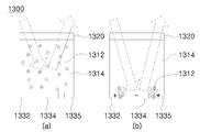
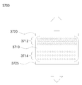
도 11은 본 발명의 일 실시예에 따라 제 1 모드의 구성을 예시적으로 나타내는 도면이다. 도 11을 참조하면, 인가되는 전기장의 세기가 클수록 입자(1112)의 간격이 좁아지고 이에 따라 입자(1112)로 이루어진 광결정으로부터 반사되는 광의 파장이 짧아질 수 있다. 따라서, 전기장의 세기 및 방향을 제어함으로써 입자(1112)로부터 반사되는 광의 파장 범위를 연속적으로 조절할 수 있게 된다. 한편, 도 11에서 하부 전극이 대 전극과 소 전극으로 분할되어서 도시되었지만 본 발명은 이로만 한정되는 것이 아니라 하부 전극이 일체화되어서 형성될 수도 있다. 즉, 각 실시예에 따라서 전극이 분할 또는 일체화될 수 있으며, 이하의 내용을 따라가면 어떠한 모드 전환 실시예에 있어서 전극이 일체화가 필요하고 전극의 분할이 필요할지 이해될 것이다. 참고로, 하나의 특정 모드 전환의 경우에, 본 발명은 동일한 단일 화소에서 모드가 전환되기 때문에, 해당 전극의 구조는 변화되지 않아야 함이 자명하다.
또한, 상기 제 1 모드를 구현하기 위해서 인가되는 전압은 직류 전압 또는 교류 전압 또는 직류 성분을 포함하는 교류 전압일 수 있다. 위에서 설명한 전기 분극 특성 또는 가변 전기 분극 특성은 교류 전압을 인가하거나 직류 전압을 인가할 경우에 모두 발생할 수 있다.특히, 대전된 입자에 직류 전압을 인가하는 경우에는 전기 영동에 의해 대전된 입자가 반대 전하로 인가된 전극으로 이동하며, 전하가 전극으로 밀집함에 따라 밀집된 전하로 인한 스크린 현상으로 다른 입자에 영향을 미치게 되어 입자들은 점진적으로 변화하는 전기 영동력을 받게 되며, 결과적으로 전기장 방향으로 점차 다른 간격을 유지하게 될 수 있고 장거리 규칙성보다는 단거리 규칙성만을 갖게 되어 시야각이 우수한 표시부를 구성할 수도 있다. 이러한 시야각 특성에 대해서는 후술될 것이다.
또한, 본 발명의 도면에서는 전압을 인가하지 않는 경우에는 입자가 무질서하게 분산되어 용액컬러를 나타내는 것으로 표시하였으나, 입자의 농도가 소정의 값보다 높아 전압을 인가하지 않은 경우에도 입자간 상호작용힘이 충분하다면, 전압을 인가하지 않아도 입자간 상호작용에 의해 특정 간격을 유지할 수 있다.
제 2 모드(고유색 반사 모드)의 동작 원리 및 구성
본 발명에 따른 표시 장치의 제 2 모드에 따르면, 복수의 입자가 용매 내에 분산된 상태에서 전극을 통하여 전기장을 인가하고 전기장의 세기, 방향, 인가시간, 인가횟수, 인가영역 중 적어도 하나를 조절하여 입자의 위치를 제어함으로써, 입자 또는 용매의 고유 컬러 또는 보유 컬러 또는 입자의 산란(light scattering)으로 인한 용액의 컬러, 또는 전극의 컬러가 가변적으로 표시된다. 단, 본 명세서 및 청구서 전체에서 전극이 투명전극인 경우에는, 전극컬러는 투명전극을 통해 나타나는 투명전극 아래의 재질의 컬러를 명시하기로 하며, 제 2 모드는 고유색 반사 모드 또는 보유색 반사 모드로 지칭될 수 있다. 여기서, 고유색이란 입자, 용매 또는 전극의 재질(material)이 백색광을 조사한 경우 반사하는 컬러를 의미할 수 있다.
본 발명에 따른 표시 장치의 제 2 모드는, 전기 영동(EP: ElectroPhoresis)을 이용하여 전하를 갖는 입자를 이동시키거나 유전 영동(DEP: DiElectroPhoresis)을 이용하여 용매와 서로 다른 소정의 유전율을 갖는 입자를 이동시킴으로써 구현될 수 있다. 이러한 전기 영동 및 유전 영동 현상은 분산된 용매에 직류 전압을 인가하는 경우 더욱 효과적으로 발생할 수 있다.
먼저, 전기 영동을 이용하여 본 발명에 따른 표지 장치의 제 2 모드를 구현하는 실시예에 대하여 살펴보기로 한다.
본 발명에 따른 표시 장치의 제 2 모드에 따르면, 동일한 부호의 전하를 갖는 복수의 입자가 용매에 분산된 상태에서 입자 및 용매에 전기장이 인가되는 경우, 입자가 갖는 전하로 인하여 복수의 입자에는 전기장의 세기와 입자의 전하량에 비례하는 전기적 인력이 작용하게 되고 이에 따라 복수의 입자는 전기 영동(electrophoresis)되어 소정 방향으로 이동하게 된다. 이때, 전압을 전극의 일부 부분에만 국부적으로 인가하거나 소정의 전압이상으로 인가하면 복수의 입자가 제 1 모드에서와 같이 광결정을 형성하지 못하고 전기장을 인가하는 전극의 국부영역 쪽으로 이동하게 된다.
도 12는 본 발명의 일 실시예에 따른 표시 장치의 제 2 모드의 구성을 예시적으로 나타내는 도면이다.
도 12를 참조하면, 전기장이 인가되지 않는 경우에는 입자가 용매 내에 불규칙하게 분산되어 있어 입자와 용매의 고유의 컬러가 혼합된 용액의 컬러가 표시될 수 있고(도 12의 (a) 참조)(즉, 입자에 의한 광 산란에 의한 용액의 컬러가 나타나는 용액 컬러 반사 모드로도 지칭될 수 있음), 입자(1210)가 관찰자 쪽인 상부 전극(1230) 쪽으로 이동하게 되어 입자(1210)가 갖는 고유의 컬러가 표시될 수 있고(도 12의 (b) 참조)(입자 컬러 반사 모드로 지칭될 수 있음), 입자(1210)가 관찰자의 반대쪽이고 넓은 면적을 갖는 제 1 하부 전극((1240)(대 전극으로 지칭됨) 쪽으로 이동하게 되어 입자(1210)가 갖는 고유의 컬러가 표시되는 대신에 용매(1220)가 갖는 고유의 컬러가 표시될 수 있으며(도 12의 (c) 참조)(용매 컬러 반사 모드로 지칭될 수 있음), 입자(1210)가 관찰자의 반대쪽이고 좁은 면적을 갖는 제 2 하부 전극(국부 전극 또는 소 전극으로 지칭될 수 있음)(1250) 쪽으로 이동하게 되어 넓은 면적을 갖는 제 1 하부 전극(1240)이 드러나게 되면 제 1 하부 전극(1240)이 갖는 고유의 컬러가 표시될 수 있다(도 12의 (d) 참조)(전극 컬러 반사 모드로 지칭됨). 제 1 하부 전극(1240)이 투명한 경우에는, 투명한 하부전극을 통해 표시되는 하부전극 밑의 재질의 컬러를 전극 컬러로 지칭하기로 한다. 한편, 도 12에서 하부 전극이 대 전극(1240)과 소 전극 또는 국부 전극(1250)으로 분할되어 있지만 도 12의 (a), (b), (c)에 대응하는 용액 컬러 반사 모드, 입자 컬러 반사 모드, 용매 컬러 반사 모드에서는 하부 전극이 일체화 구조로 되어도 무방하다. 또한, 본 도면에서는 소 전극 또는 국부 전극(1250)은 설명을 위해서 크게 도시되었지만 그 옆에 있는 대 전극(1240)에 비해서 매우 작아서 위에서 보았을 때에 대 전극이 하부 전극의 전부를 차지하고 있는 것과 같이 보일 수 있다. 또한, 본 명세서에서는 하부 전극이 대 전극과 소 전극으로 분할되어 있는 구성으로 되어 있지만 상부 전극이 대 전극과 소 전극으로 분할되는 구성도 고려할 수 있다. 가령, 상부 전극이 대 전극과 소 전극으로 분할되는 경우에 있어서, 입자 컬러 반사 모드는 대 전극에만 전압을 인가하여서 구현될 수 있으며, 전극 컬러 반사 모드에서도 역시 소 전극에만 전압을 인가하여서 구현될 수 있다, 말하자면, 본 발명의 고유색 반사 모드를 구현하는 실시예는 도 12로만 한정되는 것이 아니라 다양한 변경이 가능하다.
다음으로, 유전 영동을 이용하여 본 발명에 따른 표지 장치의 제 2 모드를 구현하는 실시예에 대하여 살펴보기로 한다.
유전 영동 현상은 불균일한 전기장이 걸려있는 유전 매질 내에 놓여있는 대전되지 않은 유전입자가 유도 쌍극자 모멘트를 가지게 되고, 유전입자의 유전상수와 유전 매질의 유전상수의 차이에 의해 유전입자에 가해지는 힘이 발생되어, 전기장 구배(gradient)가 큰 영역 또는 작은 영역으로 이동하게 되는 현상이다. 따라서, 유전매질의 유전상수보다 큰 유전상수를 갖는 유전입자는 전기장 구배가 큰 영역으로 이동하고, 유전 매질의 유전상수보다 작은 유전상수를 갖는 유전입자는 전기장 구배가 작은 영역으로 이동한다.
도 13은 본 발명의 일 실시예에 따른 표시 장치의 제 2 모드의 구성을 예시적으로 나타내는 도면이다.
도 13을 참조하면, 입자(1312)의 유전상수가 용매(1314)의 유전상수보다 크고, 하부 전극이 제1 하부 전극(1332, 1335)과 제2 하부 전극(1334)으로 나누어져 구성되는 경우를 가정할 수 있다. 도 13의 (a)를 참조하면, 전극에 전압이 인가되지 않아 입자(1312) 및 용매(1314)에 전기장이 인가되지 않는 경우에는 입자(1312)가 용매(1314) 내에서 불규칙적으로 분산되기 때문에 용액이 갖는 고유의 컬러가 표시될 수 있다. 한편, 도 13의 (b)를 참조하면, 제1 하부 전(1332, 1335)극 및 제2 하부 전극(1334)에 전압이 인가되어 제1 하부 전극(1332, 1335)이 (+) 부호의 전극이 되고 제2 하부 전극(1334)이 (-) 부호의 전극이 되는 경우에는, 제1 하부 전극(1332, 1335)과 제2 하부 전극(1334) 사이의 공간에 발생되는 전기장의 기울기가 표시부 내의 다른 영역에서 발생되는 전기장 기울기보다 월등하게 높아지기 때문에 입자(1312)가 유전 영동에 의하여 이동하여 제1 하부 전극(1332, 1335)과 제2 하부 전극(1334) 사이의 공간으로 집중되게 되고 이에 따라 제1 하부 전극(1332, 1335) 또는 제2 하부 전극(1334)이 갖는 고유의 컬러가 표시될 수 있다.
한편, 앞서 설명한 제 1 모드는 표시 장치로 입사되는 광 중 특정 파장의 광을 선택적으로 반사시키는 광결정의 원리에 의하여 동작하기 때문에, 완전한 흰색 또는 검은색을 구현하는 것이 쉽지 않다. 따라서, 제 2 모드에서 흰색 또는 검은색의 입자, 용매 또는 전극을 조합하여 사용하면, 입자, 용매 또는 전극이 갖는 고유가 컬러인 흰색이나 검은색을 완벽하게 구현해 낼 수 있으므로 위와 같은 제 1 모드의 단점을 보완할 수 있게 된다. 보다 구체적으로 흰색 입자를 사용하고 검은색 전극(전극 재질이 검은색이거나, 투명한 하부 전극의 하부에 검은색 물질이 위치)을 사용하면 상기 기술한 모드 전환에 따라 입자 컬러인 흰색과 전극 컬러인 검정색을 동일 표시 영역 혹은 동일한 단위 픽셀 또는 화소 내에서 선택적으로 구현할 수 있다.
제 3 모드(투과도 조절 모드)의 동작 원리 및 구성
본 발명에 따른 표시 장치의 제 3 모드에 따르면, 복수의 입자가 용매 내에 분산된 상태에서 전극을 통하여 전기장을 인가하고 전기장의 세기, 방향, 인가시간, 인가횟수, 인가영역 중 적어도 하나를 조절하여 입자의 간격, 위치 또는 배열을 제어함으로써 입자 및 용매 중 적어도 하나를 투과하는 광의 투과도를 조절할 수 있다. 본 발명에 따른 표시 장치의 제 3 모드는 광결정에 의한 반사광의 파장을 조절하거나(광 결정 투과도 조절 모드), 전기 영동 또는 유전 영동을 이용하여 입자를 이동시키거나(입자 영동 투과도 조절 모드) 혹은 입자의 배열 상태를 제어함(입자 정렬 투과도 조절 모드)으로써 구현될 수 있다. 이하에서는, 위와 같은 세 가지 구동원리를 이용하여 광 투과도를 조절하는 실시예에 대하여 각각 살펴보기로 한다. 본 명세서에서 제 3 모드는 투과도 조절 모드로 지칭될 수 있다. 역시, 본 투과도 조절 모드에서는 반사되는 광이 존재하겠지만 본 모드에서 지배적으로 발생하여서 관찰자가 감지할 수 있는 광은 투과되는 광임을 다시 한번 주지시키고자 한다.
도 14는 본 발명의 일 실시예에 따른 표시 장치의 제 3 모드의 구성을 예시적으로 나타내는 도면이다.
먼저, 도 14의 (a)를 참조하면, 복수의 입자가 용매 내에 분산된 상태에서 전극을 통하여 전기장을 인가하고 전기장의 세기 및 방향 중 적어도 하나를 조절하여 입자의 간격을 조절하여 입자구조(즉, 복수의 입자가 소정의 간격을 유지함으로써 형성되는 광결정)로부터 반사되는 광의 파장을 제어함에 있어서, 입자에 인가되는 전기장의 세기를 조절하여 입자의 간격이 임계값보다 좁아지게 하거나 넓어지게 하여 입자로부터 반사되는 광의 파장 범위가 가시광선 대역이 아닌 자외선이나 적외선 대역이 되도록 전기장을 조절함으로써 표시 장치의 컬러를 가시광 영역에서 투명하게 할 수 있다. 즉, 입자로 이루어진 광결정으로부터 반사되는 광을 투명하게 함으로써 광 투과도를 조절할 수 있게 된다. 참조로, 본 발명에 있어서 광투과도라 함은 주로 가시광 영역에서의 광 투과도를 의미한다. 이러한 방식을 본 명세서에서는 광 결정 투과도 조절 모드로 지칭될 수 있다. 이러한 광 결정 투과도 조절 모드는 직류 전압 및 교류 전압 모두에서 발생할 수 있으며, 입자가 분산된 용액이 상기 기술한 가변 전기 분극 특성을 가진 경우 더욱 효과적으로 나타날 수 있다. 일 실시예로, 전기 분극 특성이 우수한 강유전체나 초상유전체 입자를 사용하면 외부 전기장 인가시 전기분극된 입자들간의 상호작용으로 인해 입자들의 배열이 더욱 효과적으로 나타내어 더 강렬한 투과도가 얻어진다.
다음으로, 도 14의 (b)를 참조하면, 전기 영동에 의하여 이동하는 입자 또는 유전 영동에 의하여 이동하는 입자에 대하여 전기장을 인가하여 상대적으로 좁은 면적을 갖는 전극에 해당 입자를 집중시킴으로써 표시 장치에 입사되는 광이 입자에 의하여 반사되거나 산란되지 않도록 함으로써 광 투과도를 조절할 수 있게 된다. 한편, 본 도면에서는 도시되지 않았지만 하부 국부 전극에 입자가 집중되는 밀도를 조절함으로써 광 투과도가 조절될 수도 있다. 가령, 하부 전극의 중앙 부분에 국부 전극을 설치한 후에 이 국부 전극에 입자가 집중되는 밀도를 조절함으로써 입자 및/또는 용매를 투과하는 광의 투과도가 조절되는 구성도 역시 고려될 수 있다. 이러한 모드는 본 명세서에서는 입자 영동 투과도 조절 모드로 지칭될 수 있으며, 이 모드는 직류 전압을 인가할 때 더욱 효과적으로 이루어질 수 있으며, 직류전압을 인가한 시간 혹은 횟수에 따라 투과도를 조절 할 수도 있다.
다음으로, 도 14의 (c)를 참조하면, 전기 분극 특성을 갖는 복수의 입자가 용매 내에 분산된 상태에서 입자 및 용매에 전기장이 인가되는 경우, 복수의 입자는 전기장에 의해 분극이 유발되어 전기장의 방향에 따라 모두 동일한 방향으로 분극될 수 있는데, 동일한 방향으로 분극된 복수의 입자 사이에는 전기적 인력이 발생하기 때문에, 용매 내에 분산되어 있는 복수의 입자는 서로를 끌어 당겨 전기장의 방향과 평행한 방향으로 규칙적으로 배열될 수 있다. 따라서, 전기장의 세기 또는 방향을 조절하여 전기장의 방향과 평행한 방향으로 규칙적으로 배열되는 복수의 입자의 배열 상태를 제어함으로써 용매 및 입자에 대한 입사광의 투과도를 조절할 수 있게 된다. 본 도면에서는 입자의 정렬이 비교적 일직선으로 되어서 투과도가 우수한 경우를 상정하여서 도시되었지만 입자의 정렬 정도가 더 약한 선형의 형상을 하여서 투과도가 낮아진 경우도 역시 고려될 수 있을 것이다. 따라서, 본 모드는 입자 배열 또는 정렬 투과도 조절 모드로 지칭될 수 있으며, 이 모드는 직류전압으로도 구현될 수 있으나, 직류전압 인가시 전기 영동에 의해 전극으로 치우치는 현상을 방지하기 위해 교류 전압을 인가하여서 구현되는 것이 바람직하다. 보다 구체적으로, 입자가 전하를 갖고 직류 전기장을 이용하여 입자의 배열을 제어하는 도 14 (c) 경우에는, 입자 및 용매에 인가되는 전기장의 세기가 지나치게 커지거나 국부적으로 인가하게 되면, 앞서 설명한 제 2 모드에서와 같이 전기 영동에 의한 전기적 인력에 의하여 입자가 전극 쪽으로 이동하여 입자가 갖는 고유 컬러의 광을 반사시키거나 전극 한쪽으로 집중되는 현상이 나타날 수 있기 때문에, 직류보다는 교류 전기장을 용액에 균일하게 인가하는 것이 유리할 수 있다.
동일한 단일 화소 또는 셀 내에서의 모드 간 전환
이하에서는, 본 발명의 상기 제 1, 제 2 및 제 3 모드 중 적어도 2 개의 모드를 동일한 단일 화소 또는 셀 내에서 서로 전환 가능하게 선택적으로 구현하는 모드 전환 구성을 특정 도면을 참조하여서 기술할 것이다.
(1) 동일한 단일 화소 또는 셀 내에서의 제 1 모드와 제 2 모드 간의 전환
도 15는 본 발명의 일 실시예에 따라 동일한 단일 화소 또는 셀 내에서 제 1 및 제 2 모드를 서로 전환 가능하게 선택적으로 수행할 수 있는 표시 장치의 구성을 예시적으로 나타내는 도면이다.
도 15를 참조하면, 본 발명의 일 실시예에 따른 표시 장치(1500)는 표시부(1510) 및 전극(1520)를 포함할 수 있다. 보다 구체적으로, 표시부(1510)에는 복수의 입자(1512)가 용매(1514) 내에 분산된 채 포함될 수 있고, 전극(1520)은 상부전극(1522), 하부 전극(1524) 및 국부 전극(1526)을 포함할 수 있다. 또한, 표시부(1510) 내에 포함된 입자(1512) 및 용매(1514)와 표시부(1510)의 하부를 커버하고 있는 하부 전극(1524)는 각각 고유의 컬러를 가질 수 있다. 본 명세서에서는 설명을 위해서 표시부와 전극으로 구분하여서 설명하였지만 전극이 표시부에 포함될 수 있음은 자명하다. 즉, 표현 언어적인 측면에서 표시부와 전극을 포함한 구성을 합쳐서 표시부로 하여도 본 발명을 실시하는데 있어서 문제가 없음을 본 기술 분야의 당업자는 이해할 것이다. 또한, 표시부 또는 전극에 전기장을 인가하는 구체적 구성이 도시되지 않았지만 이는 본 기술 분야의 당업자에게 잘 알려져 있는 구성 요소이므로 본 명세서에서는 본 발명의 원리 및 취지를 모호하게 하지 않도록 그 구성을 생략하는 바이다. 중요하게는, 단일 화소 내에서 모드를 서로 전환시키기 위한 제어부 또는 이러한 제어부의 기능에 대응하는 인스트럭션을 포함하는 머신 판독 가능한 기록 매체에 대해서는 자세하세 후술될 것이다. 또한, 단일 화소는 독립적으로 제어 가능한 최소의 표시 단위임을 본 기술 분야의 당업자는 이해할 것이다. 또한, 도 15에서는 상부 전극이 투명한 전극이다.
본 발명의 일 실시예에 따르면, 표시 장치는 동일한 단일 화소 내에서 제 1 모드 및 제 2 모드 중 어느 하나의 모드를 서로 전환 가능하게 선택적으로 수행할 수 있다. 보다 구체적으로, 본 발명의 일 실시예에 따른 표시 장치는 복수의 입자가 용매 내에 분산된 상태에서 전극을 통하여 전기장을 인가하고 전기장의 세기 및 방향 중 적어도 하나를 조절할 수 있으며, 이에 따라 입자의 간격을 제어하여 입자로 이루어진 광결정으로부터 반사되는 광의 파장의 조절하거나(제 1 모드), 입자의 위치를 제어하여 용액의 색상(즉, 입자의 광 산란에 의한 용액의 색상), 입자, 용매 또는 전극의 갖는 고유의 컬러를 표시하는 기능을 수행할 수 있다(제 2 모드). 이하에서, 용액의 컬러는 입자의 광 산란에 의한 용액의 컬러를 포함하는 것으로 간주될 수 있다.
먼저, 도 15의 (a)를 참조하면, 본 발명의 일 실시예에 따른 표시 장치(1500)는 가변 분극 특성을 나타내는 용액에 전극(1522, 1524)를 통하여 인가되는 직류(DC) 전기장의 세기 또는 방향을 조절하여 입자(1512)의 간격을 제어함으로써 입자(1512)로부터 반사되는 광의 파장(즉, 컬러)를 조절할 수 있다(제 1 모드).앞서 제 1 모드와 관련하여 자세히 설명한 바와 같이, 복수의 입자(1512)가 동일한 전하를 갖는 경우에는 외부 전기장으로 인한 전기적 인력, 서로 동일한 부호의 전하를 갖는 입자(1512) 사이의 전기적 척력 및 외부 전기장에 의한 분극으로 인한 전기적 인력 등이 평형(equilibrium)을 이루는 거리를 두고 복수의 입자(1512)가 규칙적으로 배열될 수 있으며, 소정의 간격을 두고 배열된 복수의 입자(1512)는 광결정으로서의 기능을 할 수 있게 된다. 한편, 복수의 입자(1512)가 입체 장애 효과를 일으킬 수 있는 입체 장애물을 갖는 경우에는 입체 장애 효과 인한 입자 사이의 반발력 및 외부 전기장에 의한 분극으로 인한 전기적 인력 등이 평형(equilibrium)을 이루는 거리를 두고 복수의 입자(1512)가 규칙적으로 배열될 수 있으며, 소정의 간격을 두고 배열된 복수의 입자(1512)는 광결정으로서의 기능을 할 수 있게 된다.상기, 전하로 인한 반발력과 입체장애에 의한 반발효과는 동시에 발현되게 할 수도 있다.
또한, 본 발명의 일 실시예에 따른 표시 장치(1500)는, 전극(1522, 1524)를 통하여 인가되는 교류(AC) 전기장의 세기 또는 방향 또는 교류 주파수를 조절하여 입자(1512)의 간격을 제어함으로써 입자(1512)로부터 반사되는 광의 파장(즉, 컬러)를 조절할 수 있다(제 1 모드). 교류 전압을 인가하는 경우에는 인가된 교류전압에 따라 발생된 전기 분극에 따라 입자간 상호인력이 발생하고, 입자표면에 동일하게 대전된 전하 또는 입자간 입체장애 효과를 발생시키는 층에 의해 상호 척력이 발생하여 인력과 척력의 균형에 의해 입자들을 일정한 거리로 유지시킬 수 있다. 따라서, 교류전압을 인가하는 경우에는 발생되는 전기 분극이 교류전압의 주파수에 따라 충분히 변경될 수 있는 주파수 범위에서 인가되어야 한다.
이상에서 살펴본 바와 같이 일정한 간격을 두고 배열된 복수의 입자(1512)로부터 반사되는 광의 파장은 입자(1512)의 간격에 의해 결정되기 때문에, 전극(1520)를 통하여 인가되는 전기장의 세기 및 방향을 조절하여 입자(1512)의 간격을 제어함으로써 복수의 입자(1512)로부터 반사되는 광의 파장을 임의로 제어할 수 있게 된다.
다음으로, 본 발명의 일 실시예에 따른 표시 장치(1500)는 전극(1522, 1524, 1526)를 통하여 인가되는 직류(DC) 전기장의 세기 또는 방향을 조절하되, 전기장의 세기가 특정 임계치 이상이 되도록 조절하여 전기 영동 또는 유전 영동의 원리에 따라 입자(1512)를 이동시킴으로써, 용액(1512, 1514), 입자(1512), 용매(1514) 및 하부 전극(1524) 중 어느 하나가 갖는 고유의 컬러의 컬러가 표시되도록 할 수 있다(제 2 모드).
도 15의 (b)를 참조하면, 앞서 제 2 모드와 관련하여 자세히 설명한 바와 같이, 전기장이 인가되지 않는 경우 혹은 임계치보다 낮은 전압을 인가한 경우에는 입자(1512)가 용매(1514) 내에 불규칙하게 분산되어 있어 입자(1512)의 고유의 컬러, 용매(1514)의 고유의 컬러 및 입자(1512) 또는 용매(1514)로부터 반사 또는 산란되는 광의 컬러가 혼합되어 나타나는 용액의 컬러가 표시될 수 있다.
도 15의 (a)의 광 결정 반사 모드와 도 15의 (b)의 용액 컬러 반사 모드 간의 상호 전환은 인가되는 전압의 세기에 의해서 구현될 수 있다. 즉, 광 결정 반사 모드에서 사용되는 인가 전압은 용액 컬러 반사 모드에서 사용되는 인가 전압보다 클 수 있다.
이렇게 광 결정 반사 모드와 용액 컬러 반사 모드를 동일한 단일 화소 내에서 선택적으로 구현함으로써 다양한 색상이 간단한 방식 및 구조로 해서 표현될 수 있다. 이러한 광 결정 반사 모드와 용액 컬러 반사 모드 간의 전환의 실시예에서는 도 15에 도시된 바와 같이 하부 전극이 분할될 필요 없이 일체화되어 있어도 무방하다.
도 15의 (c)를 참조하면, 앞서 제 2 모드와 관련하여 자세히 설명한 바와 같이, 복수의 입자(1512)가 전하를 갖고 상부 전극(1522)이 입자(1512)가 갖는 전하와 반대 부호의 전극이 되도록 임계값 이상의 세기로 전기장이 인가되는 경우에는 전기 영동에 의해 입자(1512)가 상부 전극(1522) 쪽으로 이동하게 되고 이에 따라 표시부(1510) 상에서 입자(1512)가 갖는 고유의 컬러가 표시될 수 있다.
도 15의 (a)의 광 결정 반사 모드와 도 15의 (c)의 입자 컬러 반사 모드 간의 상호 전환은 인가되는 전압의 세기에 의해서 구현될 수 있다. 즉, 광 결정 반사 모드에서 사용되는 인가 전압은 입자 컬러 반사 모드에서 사용되는 인가 전압보다 작을 수 있다. 또는, 도 15의 (a) 광결정 모드는 교류전압을 이용하여 구현하고, 도 15의 (c)는 직류전압을 인가하여 구현할 수도 있다. 즉, 전압의 형태(직류 또는 교류)를 변화시킴으로써도 모드를 전환할 수 있다.
이렇게 광 결정 반사 모드와 입자 컬러 반사 모드를 동일한 단일 화소 내에서 선택적으로 구현함으로써 다양한 색상이 간단한 방식 및 구조로 해서 표현될 수 있다. 이러한 광 결정 반사 모드와 용액 컬러 반사 모드 간의 전환의 실시예에서는 도 15에 도시된 바와 같이 하부 전극이 분할될 필요 없이 일체화되어 있어도 무방하다.
도 15의 (d)를 참조하면, 앞서 제 2 모드와 관련하여 자세히 설명한 바와 같이, 복수의 입자(1512)가 전하를 갖고 하부 전극(1524)이 입자(1512)가 갖는 전하와 반대 부호의 전극이 되도록 임계값 이상의 세기로 전기장이 인가되는 경우에는 전기 영동에 의해 입자(1512)가 하부 전극(1524) 쪽으로 이동하게 되고 이에 따라 표시부(1510) 상에서 용매(1512)가 갖는 고유의 컬러가 표시될 수 있다.
도 15의 (a)의 광 결정 반사 모드와 도 15의 (d)의 용매 컬러 반사 모드 간의 상호 전환은 인가되는 전압의 방향에 의해서 구현될 수 있다. 즉, 대전된 입자가 상부전극으로 이동하게 인가하는 경우에는, 전기장의 세기에 따라 광 결정 반사 모드가 구현되고, 대전된 입자가 하부전극으로 이동하게 인가하는 경우에는 용매 컬러 반사 모드가 구현될 수 있다.
이렇게 광 결정 반사 모드와 용매 컬러 반사 모드를 동일한 단일 화소 내에서 선택적으로 구현함으로써 다양한 색상이 간단한 방식 및 구조로 해서 표현될 수 있다. 이러한 광 결정 반사 모드와 용매 컬러 반사 모드 간의 전환의 실시예에서는 도 15에 도시된 바와 같이 하부 전극이 분할될 필요 없이 일체화되어 있어도 무방하다.
도 15의 (e)를 참조하면, 앞서 제 2 모드와 관련하여 자세히 설명한 바와 같이, 복수의 입자(1512)가 전하를 갖고 국부 전극(1526)이 입자(1512)가 갖는 전하와 반대 부호의 전극이 되도록 전기장이 인가되는 경우에는 전기 영동에 의해 입자(1512)가 국부 전극(1526) 쪽으로 이동하여 국부 전극(1526) 주변에 집중하여 위치하게 되고 이에 따라 표시부(1510) 상에서 하부 전극(1524)이 갖는 고유의 컬러(하부전극이 투명한 경우, 하부전극 밑의 재질의 컬러)가 표시될 수 있다.
도 15의 (a)의 광 결정 반사 모드와 도 15의 (e)의 전극 컬러 반사 모드 간의 상호 전환은 인가되는 전압이 인가되는 인가영역에 의해서 구현될 수 있다. 즉, 광 결정 반사 모드에서는 전기장을 균일하게 인가하지만, 전극 컬러 반사 모드에서는 표시부 전극의 국부적인 영역에만 인가하여 구현될 수 있다. 인가되는 전기장의 세기는 광 결정 반사 모드가 전극 컬러 반사 모드보다 더 약할 수 있다.
이렇게 광 결정 반사 모드와 전극 컬러 반사 모드를 동일한 단일 화소 내에서 선택적으로 구현함으로써 다양한 색상이 간단한 방식 및 구조로 해서 표현될 수 있다. 이러한 광 결정 반사 모드와 전극 컬러 반사 모드 간의 전환의 실시예에서는 도 15에 도시된 바와 같이 하부 전극이 분할되지 않고 상부 전극이 분할되어서도 구현될 수 있으며, 분할 전극의 형태는 도 15에 국한되지 않고 다양한 형태 또는 복수의 국부적 영역에만 인가할 수도 있다.
특히, 상술한 바와 같이 제 1 모드에서는 백색 및 흑색의 컬러가 구현되기 어렵다. 따라서, 제 2 모드에서 용매, 입자, 전극의 컬러(투명전극인 경우 하부 전극 하부의 재질의 컬러)를 백색 및 흑색을 조합하여서 사용함으로써 동일한 단일 화소 또는 동일 표시영역에서 연속적인 색상의 컬러 및 백색 및 흑색을 모두 구현(rendering)할 수 있다.
한편, 제 1 모드 및 제 2 모드가 수행되는 경우에 대한 실시예와 제 1 모드 및 제 2 모드 중 어느 하나의 모드가 동일한 단일 화소 내에서 다른 모드로 전환되는 경우에 대한 실시예에 대하여 더욱 구체적으로 살펴보면 다음과 같다.
먼저, 입자가 동일한 부호의 전하를 갖는 경우를 가정할 수 있다. 이러한 경우, 전기장이 인가되지 않거나 임계치 전압 이하이면, 입자가 용매 내에 불규칙하게 분산되어 용액의 컬러가 표시되는 제 2 모드가 수행될 수 있다. 또한, 전기장이 직류 전기장이고 직류 전기장의 세기가 입자의 간격을 규칙적으로 제어할 수 있는 범위 내에서 조절되면, 직류 전기장의 세기에 따라 입자로부터 반사되는 광의 파장이 가시광선 대역 내에서 조절되는 제 1 모드가 수행될 수 있다. 또한, 전기장이 직류 전기장이고 전기장의 세기가 전기 영동(electrophoresis)에 의해 입자를 전극 쪽으로 집중시킬 수 있는 임계값 이상이면, 입자가 상부 전극에 집중되어 입자의 컬러가 표시되거나 입자가 하부 전극에 집중되어 용매의 컬러가 표시되거나 입자가 국부 전극에 집중되어 상부 전극 또는 하부 전극의 컬러가 표시되는 제 2 모드가 수행될 수 있다.
또한, 전기장이 교류 전기장이고 교류 전기장의 세기 및 주파수가 입자의 간격을 규칙적으로 제어할 수 있는 범위 내에서 조절되면, 교류 전기장의 세기 또는 주파수에 따라 입자로부터 반사되는 광의 파장이 가시광선 대역 내에서 조절되는 제 1 모드가 수행될 수 있다. 교류 전압을 인가할 시에는 교류 전압의 세기뿐만 아니라 주파수도 역시 광 결정 모드의 입자 간격을 조절하는데 사용되는 변수가 될 수 있다. 또한, 제 1 모드에서는 교류 전압을 인가하여서 광 결정 반사 모드를 구현하고 제 2 모드 중 용매 컬러 반사 모드, 입자 컬러 반사 모드 및 전극 컬러 반사 모드에서는 직류 전압을 인가하여서 구현될 수 있다. 이러한 경우 용액(입자 또는 용매 또는 이들의 조합)이 전기 분극 특성을 나타내는 경우 광결정 모드 구현을 더욱 용이하게 할 수 있다.
다음으로, 입자가 전기 분극 특성(전기장이 인가되면 전기 분극이 유발되며 인가된 전기장이 변화함에 따라 전기 분극량이 변화됨)을 갖고 입체 장애 효과를 발생시키는 구조를 포함하는 다른 경우를 가정할 수 있다. 이러한 경우, 전기장이 인가되지 않거나 임계치 이하이면, 입자가 용매 내에 불규칙하게 분산되어 용액의 컬러가 표시되는 제 2 모드가 수행될 수 있다. 또한, 전기장이 직류 전기장이고 직류 전기장의 세기가 입자의 간격을 규칙적으로 제어할 수 있는 범위 내에서 조절되면, 직류 전기장의 세기에 따라 입자로부터 반사되는 광의 파장이 가시광선 대역 내에서 조절되는 제 1 모드가 수행될 수 있다. 또한, 전기장의 분포가 불균일 하고 입자와 용매의 유전율이 다른 경우에는, 유전 영동(dielectrophoresis)에 의해 입자를 전극 쪽으로 집중시킬 수 있는 임계값이 이상으로 직류 전기장을 인가하면, 입자가 상부 전극에 집중되어 입자의 컬러가 표시되거나 입자가 하부 전극에 집중되어 용매의 컬러가 표시되거나 입자가 국부 전극에 집중되어 상부 전극 또는 하부 전극의 컬러가 표시되는 제 2 모드가 수행될 수 있다. 또한, 전기장이 교류 전기장이고 교류 전기장의 세기 및 주파수가 입자의 간격을 규칙적으로 제어할 수 있는 범위 내에서 조절되면, 교류 전기장의 세기 또는 주파수에 따라 입자로부터 반사되는 광의 파장이 가시광선 대역 내에서 조절되는 제 1 모드가 수행될 수 있다.
도면에서는 특정하게 도시되지 않았지만, 광 결정 반사 모드에서 용액 컬러 반사 모드, 입자 컬러 반사 모드, 전극 컬러 반사 모드 또는 용매 컬러 반사 모드로 전환되는 것을 물론, 용액 컬러 반사 모드, 입자 컬러 반사 모드, 전극 컬러 반사 모드 및 용매 컬러 반사 모드 간에서도 서로 전환 가능하다. 이렇게 제 2 모드 간에서 전환되는 구성이 이하에서 설명될 것이다.
(2) 동일한 단일 화소 또는 셀 내에서의 제 1 모드와 제 3 모드 간의 전환
도 16은 본 발명의 일 실시예에 따라 제 1 및 제 3 모드를 동일한 단일 화소 내에서 서로 전환 가능하게 선택적으로 수행할 수 있는 표시 장치의 구성을 예시적으로 나타내는 도면이다.
도 16을 참조하면, 본 발명의 일 실시예에 따른 표시 장치(1600)는 표시부(1610) 및 전극(1620)를 포함할 수 있다. 보다 구체적으로, 표시부(1610)에는 복수의 입자(1612)가 용매(1614) 내에 분산된 채 포함될 수 있고, 전극(1620)은 상부전극(1622), 하부 전극(1624) 및 국부 전극(1626)을 포함할 수 있다. 또한, 상부전극(1622), 하부 전극(1624) 및 국부 전극(1626)은 모두 광 투과성 물질로 구성되어 표시 장치(1600)로 입사되는 광을 투과시킬 수 있다.
본 발명의 일 실시예에 따르면, 표시 장치는 제 1 모드 및 제 3 모드 중 어느 하나의 모드를 서로 전환 가능하게 선택적으로 수행할 수 있다. 보다 구체적으로, 본 발명의 일 실시예에 다른 표시 장치는 복수의 입자가 용매 내에 분산된 상태에서 전극을 통하여 전기장을 인가하고 전기장의 세기 및 방향 중 적어도 하나를 조절할 수 있으며, 이에 따라 입자의 간격을 제어하여 입자로 이루어진 광결정으로부터 반사되는 광의 파장의 조절하거나(제 1 모드), 입자의 간격, 위치 또는 배열을 제어하여 표시 장치로 입사되는 광의 투과도를 조절하는(제 3 모드) 기능을 수행할 수 있다.
먼저, 도 16의 (a)를 참조하면, 본 발명의 일 실시예에 따른 표시 장치(1600)는 전극(1622, 1624)를 통하여 인가되는 직류(DC) 전기장의 세기 또는 방향을 조절하여 입자(1612)의 간격을 제어함으로써 입자(1612)로부터 반사되는 광의 파장(즉, 컬러)를 조절할 수 있다(제 1 모드).
앞서 제 1 모드와 관련하여 자세히 설명한 바와 같이, 복수의 입자(1612)가 동일한 전하를 갖는 경우에는 외부 전기장으로 인한 전기적 인력, 서로 동일한 부호의 전하를 갖는 입자(1612) 사이의 전기적 척력 및 외부 전기장에 의한 분극으로 인한 전기적 인력 등이 평형(equilibrium)을 이루는 거리를 두고 복수의 입자(1612)가 규칙적으로 배열될 수 있으며, 소정의 간격을 두고 배열된 복수의 입자(1612)는 광결정으로서의 기능을 할 수 있게 된다. 한편, 복수의 입자(1612)가 입체 장애 효과를 일으킬 수 있는 입체 장애물을 갖는 경우에는 입체 장애 효과 인한 입자 사이의 반발력 및 외부 전기장에 의한 분극으로 인한 전기적 인력 등이 평형(equilibrium)을 이루는 거리를 두고 복수의 입자(1612)가 규칙적으로 배열될 수 있으며, 소정의 간격을 두고 배열된 복수의 입자(1612)는 광결정으로서의 기능을 할 수 있게 된다.
또한, 본 발명의 일 실시예에 따른 표시 장치(1600)는, 전극(1622, 1624)를 통하여 인가되는 교류(AC) 전기장의 세기 또는 방향 또는 주파수를 조절하여 입자(1612)의 간격을 제어함으로써 입자(1612)로부터 반사되는 광의 파장(즉, 컬러)를 조절할 수 있다(제 1 모드).
이상에서 살펴본 바와 같이 일정한 간격을 두고 배열된 복수의 입자(1612)로부터 반사되는 광의 파장은 입자(1612)의 간격에 의해 결정되기 때문에, 전극(1620)를 통하여 인가되는 전기장의 세기 및 방향을 조절하여 입자(1612)의 간격을 제어함으로써 복수의 입자(1612)로부터 반사되는 광의 파장을 임의로 제어할 수 있게 된다.
다음으로, 본 발명의 일 실시예에 따른 표시 장치(1600)는 전극(1622, 1624, 1626)를 통하여 인가되는 전기장의 세기 또는 방향 또는 인가 위치를 조절하여 입자의 간격, 위치 또는 배열을 제어함으로써 표시 장치에 입사되는 광의 투과도가 제어되도록 할 수 있다(제 3 모드 또는 투과도 조절 모드).
도 16의 (b)를 참조하면, 앞서 제 3 모드와 관련하여 자세히 설명한 바와 같이, 소정의 간격을 두고 배치된 입자(1612)로 이루어진 광결정에 대하여 특정 임계치 이상 또는 이하의 세기의 전기장을 인가하여 입자(1612)로 이루어진 광결정으로부터 자외선 또는 적외선 대역의 광은 반사되되 가시광선 대역의 광은 반사되지 않도록 함으로써, 표시 장치(1600)로 입사되는 가시광선 대역의 광이 표시 장치(1600)를 높은 광 투과율로 투과할 수 있게 된다. 이러한 모드는 상술한 바와 같이 광 결정 투과도 조절 모드로 지칭될 수 있다.
도 16의 (a)의 광 결정 반사 모드와 도 16의 (b)의 광 결정 투과도 조절 모드 간의 상호 전환은 인가되는 전압의 세기에 의해서 구현될 수 있다. 즉, 광 결정 반사 모드에서 사용되는 인가 전압은 광 결정 투과도 조절 모드에서 사용되는 인가 전압보다 클 수 있으며 작을 수도 있다. 자외선의 광 결정 투과도 조절 모드는 광 결정 반사 모드에서보다 인가되는 전압이 클 수 있으며 적외선의 광 결정 투과도 조절 모드는 반대이다.
이렇게 광 결정 반사 모드와 광 결정 투과도 조절 모드를 동일한 단일 화소 내에서 선택적으로 구현함으로써 다양한 색상 및 투과도가 간단한 방식 및 구조로 해서 표현될 수 있다. 이러한 광 결정 반사 모드와 광 결정 투과도 조절 모드 간의 전환의 실시예에서는 도 16에 도시된 바와 같이 하부 전극이 분할될 필요 없이 일체화되어 있어도 무방하다.
도 16의 (c)를 참조하면, 앞서 제 3 모드와 관련하여 자세히 설명한 바와 같이, 복수의 입자(1612)가 전하를 갖고 국부 전극(1626)이 입자(1612)가 갖는 전하와 반대 부호의 전극이 되도록 전기장이 인가되는 경우에는 전기 영동에 의해 입자(1612)가 국부 전극(1626) 쪽으로 이동하여 국부 전극(1626) 주변에 집중하여 위치하게 되고 이에 따라 표시 장치(1600)로 입사되는 광이 입자에 의하여 반사 또는 산란되지 않고 높은 표시 장치(1600)를 광 투과율로 투과할 수 있게 된다. 한편, 본 도면에서는 도시되지 않았지만 하부 국부 전극에 입자가 집중되는 밀도를 조절함으로써 광 투과도가 조절될 수도 있다. 가령, 하부 전극의 중앙 부분에 국부 전극을 설치한 후에 이 국부 전극에 입자가 집중되는 밀도를 조절함으로써 입자 및/또는 용매를 투과하는 광의 투과도가 조절되는 구성도 역시 고려될 수 있다. 이러한 모드는 본 명세서에서는 입자 영동 투과도 조절 모드로 지칭될 수 있으며, 이 모드 역시 교류 전압 및 직류 전압을 인가하여서 이루어질 수 있다.
도 16의 (a)의 광 결정 반사 모드와 도 16의 (c)의 입자 영동 투과도 조절 모드 간의 상호 전환은 인가되는 전압의 세기에 의해서 구현될 수 있다. 즉, 광 결정 반사 모드에서 사용되는 인가 전압은 입자 영동 투과도 조절 모드에서 사용되는 인가 전압보다 작을 수도 있다.
이렇게 광 결정 반사 모드와 입자 영동 투과도 조절 모드를 동일한 단일 화소 내에서 선택적으로 구현함으로써 다양한 색상 및 투과도가 간단한 방식 및 구조로 해서 표현될 수 있다. 이러한 광 결정 반사 모드와 입자 영동 투과도 조절 모드 간의 전환의 실시예에서는 도 16에 도시된 바와 같이 하부 전극이 분할되지 않고 상부 전극이 분할되어도 무방하다.
한편, 도 16의 (d)를 참조하면, 앞서 제 3 모드와 관련하여 자세히 설명한 바와 같이, 전기 분극 특성을 갖는 복수의 입자(1612)가 용매(1614) 내에 분산된 상태에서 입자(1612) 및 용매(1614)에 전기장이 인가되는 경우, 복수의 입자(1612)는 전기장에 의해 분극이 유발되어 전기장의 방향에 따라 모두 동일한 방향으로 분극될 수 있는데, 동일한 방향으로 분극된 복수의 입자(1612) 사이에는 전기적 인력이 발생하기 때문에, 용매(1614) 내에 분산되어 있는 복수의 입자(1612)는 서로를 끌어당겨 전기장의 방향과 평행한 방향으로 규칙적으로 배열될 수 있다. 따라서, 전기장의 세기 또는 방향을 조절하여 전기장의 방향과 평행한 방향으로 규칙적으로 배열되는 복수의 입자(1612)의 배열 상태를 제어함으로써 표시 장치(1600)로 입사되는 광의 투과도를 조절할 수 있게 된다. 이러한 모드는 입자 정렬 또는 배열 투과도 조절 모드로 지칭된다.
도 16의 (a)의 광 결정 반사 모드와 도 16의 (d)의 입자 정렬 투과도 조절 모드 간의 상호 전환은 인가되는 전압의 세기에 의해서 구현될 수 있다. 즉, 일 실시예에 따라서, 입자 정렬 투과도 조절 모드에서 인가되는 전압은 광 결정 반사 모드에서 인가되는 전압보다 클 수 있다.
이렇게 광 결정 반사 모드와 입자 정렬 투과도 조절 모드를 동일한 단일 화소 내에서 선택적으로 구현함으로써 다양한 색상 및 투과도가 간단한 방식 및 구조로 해서 표현될 수 있다. 이러한 광 결정 반사 모드와 입자 정렬 투과도 조절 모드 간의 전환의 실시예에서는 도 16에 도시된 바와 같이 하부 전극이 분할될 필요 없이 일체화되어 있어도 무방하다.
한편, 제 1 모드 및 제 3 모드가 수행되는 경우에 대한 실시예와 제 1 모드 및 제 3 모드 중 어느 하나의 모드가 다른 모드로 전환되는 경우에 대한 실시예에 대하여 더 구체적으로 살펴보면 다음과 같다.
먼저, 입자가 동일한 부호의 전하를 갖고, 전극은 광 투과성 물질을 포함하는 경우를 가정할 수 있다. 이러한 경우, 전기장이 직류 전기장이고 직류 전기장의 세기가 입자의 간격을 규칙적으로 제어할 수 있는 범위 내에서 조절되면, 직류 전기장의 세기에 따라 입자로부터 반사되는 광의 파장이 가시광선 대역 내에서 조절되는 제 1 모드가 수행되거나 입자로부터 반사되는 광의 파장이 가시광선 대역 외에서 조절되어 입사광의 광 투과도가 조절되는 제 3 모드가 수행될 수 있다. 또한, 전기장이 직류 전기장이고 직류 전기장의 세기가 전기 영동(electrophoresis)에 의해 입자를 전극 쪽으로 집중시킬 수 있는 임계값 이상이면, 입자가 국부 전극에 집중되어 입사광의 광 투과도가 조절되는 제 3 모드가 수행될 수 있다. 또한, 전기장이 직류 전기장이고 직류 전기장의 세기가 직류 전기장의 방향과 평행한 방향으로 입자를 배열시킬 수 있는 범위 내에서 조절되면, 입자가 입사광의 진행 방향과 소정의 각도를 이루는 상태로 배열되어 입사광의 투과도가 조절되는 제 3 모드가 수행될 수 있다. 또한, 전기장이 교류 전기장이고 교류 전기장의 세기 및 주파수가 입자의 간격을 규칙적으로 제어할 수 있는 범위 내에서 조절되면, 교류 전기장의 세기 또는 주파수에 따라 입자로부터 반사되는 광의 파장이 가시광선 대역 내에서 조절되는 제 1 모드가 수행되거나 입자로부터 반사되는 광의 파장이 가시광선 대역 외에서 조절되어 입사광의 광 투과도가 조절되는 제 3 모드가 수행될 수 있다. 또한, 전기장이 교류 전기장이고 교류 전기장의 세기 및 주파수가 교류 전기장의 방향과 평행한 방향으로 입자를 배열시킬 수 있는 범위 내에서 조절되는 경우에, 입자가 입사광의 진행 방향과 소정의 각도를 이루는 상태로 배열되어 입사광의 투과도가 조절되는 제 3 모드가 수행될 수 있다.
일 실시예에서는, 전압을 인가했을 때에, 전압의 크기를 큰 순서로 말하자면, 입자 영동 투과도 조절 모드 > 입자 정렬 투과도 조절 모드 > 자외선 반사의 광 결정 투과도 조절 모드> 가시광 광 결정 반사 모드 > 적외선 반사의 광 결정 투과도 조절 모드의 순서이며, 상기 모드는 서로 혼합되어 나타날 수도 있으며 주요하게 나타내는 효과가 변화되는 것을 의미한다.
또한, 광 결정 반사 모드, 광 결정 투과도 조절 모드 및 입자 정렬 투과도 조절 모드에서는 교류 전압이 사용되고 입자 영동 투과도 조절 모드에서는 직류 전압이 사용될 수 있다.
다음으로, 입자가 전기 분극 특성(전기장이 인가되면 전기 분극이 유발되며 인가된 전기장이 변화함에 따라 전기 분극량이 변화됨)을 갖고 입체 장애 효과를 발생시키는 구조를 포함하고, 전극은 광 투과성 물질을 포함하는 다른 경우를 가정할 수 있다. 이러한 경우, 전기장이 직류 전기장이고 직류 전기장의 세기가 입자의 간격을 규칙적으로 제어할 수 있는 범위 내에서 조절되면, 직류 전기장의 세기에 따라 입자로부터 반사되는 광의 파장이 가시광선 대역 내에서 조절되는 제 1 모드가 수행되거나 입자로부터 반사되는 광의 파장이 가시광선 대역 외에서 조절되어 입사광의 광 투과도가 조절되는 제 3 모드가 수행될 수 있다. 또한, 전기장이 직류 전기장이고 직류 전기장의 세기가 유전 영동(dielectrophoresis)에 의해 입자를 전극 쪽으로 집중시킬 수 있는 임계값 이상이면, 입자가 국부 전극에 집중되어 입사광의 광 투과도가 조절되는 제 3 모드가 수행될 수 있다. 또한, 전기장이 직류 전기장이고 직류 전기장의 세기가 직류 전기장의 방향과 평행한 방향으로 입자를 배열시킬 수 있는 범위 내에서 조절되면, 입자가 입사광의 진행 방향과 소정의 각도를 이루는 상태로 배열되어 입사광의 투과도가 조절되는 제 3 모드가 수행될 수 있다. 또한, 전기장이 교류 전기장이고 교류 전기장의 세기 및 주파수가 입자의 간격을 규칙적으로 제어할 수 있는 범위 내에서 조절되면, 교류 전기장의 세기에 따라 입자로부터 반사되는 광의 파장이 가시광선 대역 내에서 조절되는 제 1 모드가 수행되거나 입자로부터 반사되는 광의 파장이 가시광선 대역 외에서 조절되어 입사광의 광 투과도가 조절되는 제 3 모드가 수행될 수 있다. 또한, 전기장이 교류 전기장이고 교류 전기장의 세기 및 주파수가 교류 전기장의 방향과 평행한 방향으로 입자를 배열시킬 수 있는 범위 내에서 조절되는 경우에, 입자가 입사광의 진행 방향과 소정의 각도를 이루는 상태로 배열되어 입사광의 투과도가 조절되는 제 3 모드가 수행될 수 있다.
도면에서는 특정하게 도시되지 않았지만, 입자 정렬 투과도 조절 모드, 입자 영동 투과도 조절 모드 및 광 결정 투과도 조절 모드 간에서도 서로 전환 가능하다. 이렇게 제 3 모드 간에서 전환되는 구성이 이하에서 설명될 것이다.
(3) 동일한 단일 화소 또는 셀 내에서 제 2 모드와 제 3 모드 간의 전환
도 17은 본 발명의 일 실시예에 따라 제 2 및 제 3 모드를 동일한 단일 화소 내에서 서로 전환 가능하게 선택적으로 수행할 수 있는 표시 장치의 구성을 예시적으로 나타내는 도면이다.
도 17을 참조하면, 본 발명의 일 실시예에 따른 표시 장치(1700)는 표시부(1710) 및 전극(1720)를 포함할 수 있다. 보다 구체적으로, 표시부(1710)에는 복수의 입자(1712)가 용매(1714) 내에 분산된 채 포함될 수 있고, 전극(1720)은 상부전극(1722), 하부 전극(1724) 및 국부 전극(1726)을 포함할 수 있다. 또한, 표시부(1710) 내에 포함된 입자(1712) 및 용매(1714)는 각각 고유의 컬러를 가질 수 있고, 상부전극(1722), 하부 전극(1724) 및 국부 전극(1726)은 모두 광 투과성 물질로 구성되어 표시 장치(1700)로 입사되는 광을 투과시킬 수 있다.
본 발명의 일 실시예에 따르면, 표시 장치는 제 2 모드 및 제 3 모드 중 어느 하나의 모드를 서로 전환 가능하게 선택적으로 수행할 수 있다. 보다 구체적으로, 본 발명의 일 실시예에 다른 표시 장치는 복수의 입자가 용매 내에 분산된 상태에서 전극을 통하여 전기장을 인가하고 전기장의 세기 및 방향 중 적어도 하나를 조절할 수 있으며, 입자의 위치를 제어하여 용액, 입자 또는 용매가 갖는 고유의 컬러를 표시하거나(제 2 모드), 입자의 간격, 위치 또는 배열을 제어하여 표시 장치로 입사되는 광의 투과도를 조절하는(제 3 모드) 기능을 수행할 수 있다.
먼저, 본 발명의 일 실시예에 따른 표시 장치(1700)는 전극(1722, 1724, 1726)를 통하여 인가되는 직류(DC) 전기장의 세기 또는 방향을 조절하되, 전기장의 세기가 특정 임계치 이상이 되도록 조절하여 전기 영동 또는 유전 영동의 원리에 따라 입자(1712)를 이동시킴으로써, 용액(1712, 1714), 입자(1712) 및 용매(1714) 중 어느 하나가 갖는 고유의 컬러의 컬러가 표시되도록 할 수 있다(제 2 모드).
도 17의 (a)를 참조하면, 앞서 제 2 모드와 관련하여 자세히 설명한 바와 같이, 전기장이 인가되지 않는 경우에는 입자(1712)가 용매(1714) 내에 불규칙하게 분산되어 있어 입자(1712)의 고유의 컬러, 용매(1714)의 고유의 컬러 및 입자(1712) 또는 용매(1714)로부터 반사 또는 산란되는 광의 컬러가 혼합되어 나타나는 용액의 컬러가 표시될 수 있다. 이 모드는 용액 컬러 반사 모드이다.
도 17의 (b)를 참조하면, 앞서 제 2 모드와 관련하여 자세히 설명한 바와 같이, 복수의 입자(1712)가 전하를 갖고 상부 전극(1722)이 입자(1712)가 갖는 전하와 반대 부호의 전극이 되도록 전기장이 인가되는 경우에는 전기 영동에 의해 입자(1712)가 상부 전극(1722) 쪽으로 이동하게 되고 이에 따라 표시부(1710) 상에서 입자(1712)가 갖는 고유의 컬러가 표시될 수 있다. 이 모드는 입자 컬러 반사 모드이다.
도 17의 (c)를 참조하면, 앞서 제 2 모드와 관련하여 자세히 설명한 바와 같이, 복수의 입자(1712)가 전하를 갖고 하부 전극(1724)이 입자(1712)가 갖는 전하와 반대 부호의 전극이 되도록 전기장이 인가되는 경우에는 전기 영동에 의해 입자(1712)가 하부 전극(1724) 쪽으로 이동하게 되고 이에 따라 표시부(1710) 상에서 용매(1712)가 갖는 고유의 컬러가 표시될 수 있다. 이 모드는 용매 컬러 반사 모드이다.
다음으로, 본 발명의 일 실시예에 따른 표시 장치(1700)는 전극(1722, 1724, 1726)를 통하여 인가되는 전기장의 세기 또는 방향을 조절하여 입자의 간격, 위치 또는 배열을 제어함으로써 표시 장치에 입사되는 광의 투과도가 제어되도록 할 수 있다(제 3 모드).
도 17의 (d)를 참조하면, 앞서 제 3 모드와 관련하여 자세히 설명한 바와 같이, 소정의 간격을 두고 배치된 입자(1712)로 이루어진 광결정에 대하여 특정 임계치 이상 또는 이하의 세기의 전기장을 인가하여 입자(1712)로 이루어진 광결정으로부터 자외선 또는 적외선 대역의 광은 반사되되 가시광선 대역의 광은 반사되지 않도록 함으로써, 표시 장치(1700)로 입사되는 가시광선 대역의 광이 표시 장치(1700)를 높은 광 투과율로 투과할 수 있게 된다. 이 모드는 광 결정 투과도 조절 모드이다.
도 17의 (e)를 참조하면, 앞서 제 3 모드와 관련하여 자세히 설명한 바와 같이, 복수의 입자(1712)가 전하를 갖고 국부 전극(1726)이 입자(1712)가 갖는 전하와 반대 부호의 전극이 되도록 전기장이 인가되는 경우에는 전기 영동에 의해 입자(1712)가 국부 전극(1726) 쪽으로 이동하여 국부 전극(1726) 주변에 집중하여 위치하게 되고 이에 따라 표시 장치(1700)로 입사되는 광이 입자에 의하여 반사 또는 산란되지 않고 높은 표시 장치(1700)를 광 투과율로 투과할 수 있게 된다. 이 모드는 입자 영동 투과도 조절 모드이다.
한편, 도 17의 (f)를 참조하면, 앞서 제 3 모드와 관련하여 자세히 설명한 바와 같이, 전기 분극 특성을 갖는 복수의 입자(1712)가 용매(1714) 내에 분산된 상태에서 입자(1712) 및 용매(1714)에 전기장이 인가되는 경우, 복수의 입자(1712)는 전기장에 의해 분극이 유발되어 전기장의 방향에 따라 모두 동일한 방향으로 분극될 수 있는데, 동일한 방향으로 분극된 복수의 입자(1712) 사이에는 전기적 인력이 발생하기 때문에, 용매(1714) 내에 분산되어 있는 복수의 입자(1712)는 서로를 끌어 당겨 전기장의 방향과 평행한 방향으로 규칙적으로 배열될 수 있다. 따라서, 전기장의 세기 또는 방향을 조절하여 전기장의 방향과 평행한 방향으로 규칙적으로 배열되는 복수의 입자(1712)의 배열 상태를 제어함으로써 표시 장치(1700)로 입사되는 광의 투과도를 조절할 수 있게 된다. 이 모드는 입자 정렬 투과도 조절 모드이다.
먼저, 상기 용액 컬러 반사 모드와 광 결정 투과도 조절 모드 간의 전환을 살펴보면, 인가되는 전압의 크기는 광 결정 투과도 조절 모드에서 크고 용액 컬러 반사 모드에서는 전압이 인가되지 않을 수도 있다. 동일한 단일 화소 내에서 이렇게 용액 컬러 반사 모드와 광 결정 투과도 조절 모드 간의 전환으로 인해서 단일 화소를 사용하여서 색상 및 투과도를 모두 조절할 수 있게 된다.
다음으로, 상기 용액 컬러 반사 모드와 입자 영동 투과도 조절 모드 간의 전환을 살펴보면, 인가되는 전압의 크기는 입자 영동 투과도 조절 모드에서 크고 용액 컬러 반사 모드에서는 전압이 인가되지 않을 수도 있다. 동일한 단일 화소 내에서 이렇게 용액 컬러 반사 모드와 입자 영동 투과도 조절 모드 간의 전환으로 인해서 단일 화소를 사용하여서 색상 및 투과도를 모두 조절할 수 있게 된다.
다음으로, 상기 용액 컬러 반사 모드와 입자 정렬 투과도 조절 모드 간의 전환을 살펴보면, 인가되는 전압의 크기는 입자 정렬 투과도 조절 모드에서 크고 용액 컬러 반사 모드에서는 전압이 인가되지 않을 수도 있다. 동일한 단일 화소 내에서 이렇게 용액 컬러 반사 모드와 입자 정렬 투과도 조절 모드 간의 전환으로 인해서 단일 화소를 사용하여서 색상 및 투과도를 모두 조절할 수 있게 된다.
다음으로, 상기 입자 컬러 반사 모드와 광 결정 투과도 조절 모드 간의 전환을 살펴보면, 인가되는 전압의 크기는 광 결정 투과도 조절 모드보다 입자 컬러 반사 모드에서가 크다. 동일한 단일 화소 내에서 이렇게 입자 컬러 반사 모드와 광 결정 투과도 조절 모드 간의 전환으로 인해서 단일 화소를 사용하여서 색상 및 투과도를 모두 조절할 수 있게 된다.
다음으로, 상기 입자 컬러 반사 모드와 입자 영동 투과도 조절 모드 간의 전환을 살펴보면, 인가되는 전압의 크기는 동일하거나 서로 상이할 수 있지만 인가되는 전압의 방향이 상이하다. 동일한 단일 화소 내에서 이렇게 입자 컬러 반사 모드와 입자 영동 투과도 조절 모드 간의 전환으로 인해서 단일 화소를 사용하여서 색상 및 투과도를 모두 조절할 수 있게 된다.
다음으로, 상기 입자 컬러 반사 모드와 입자 정렬 투과도 조절 모드 간의 전환을 살펴보면, 인가되는 전압의 크기는 입자 정렬 투과도 조절 모드보다 입자 컬러 반사 모드에서가 크다. 동일한 단일 화소 내에서 이렇게 입자 컬러 반사 모드와 입자 정렬 투과도 조절 모드 간의 전환으로 인해서 단일 화소를 사용하여서 색상 및 투과도를 모두 조절할 수 있게 된다.
다음으로, 상기 용매 컬러 반사 모드와 광 결정 투과도 조절 모드 간의 전환을 살펴보면, 인가되는 전압의 크기는 광 결정 투과도 조절 모드보다 용매 컬러 반사 모드에서가 크다. 동일한 단일 화소 내에서 이렇게 용매 컬러 반사 모드와 광 결정 투과도 조절 모드 간의 전환으로 인해서 단일 화소를 사용하여서 색상 및 투과도를 모두 조절할 수 있게 된다.
다음으로, 상기 용매 컬러 반사 모드와 입자 영동 투과도 조절 모드 간의 전환을 살펴보면, 인가되는 전압의 크기 및 방향은 동일할 수 있지만 전압이 인가되는 전극이 상이하다. 즉, 용매 컬러 반사 모드에서는 대 전극으로 전압이 인가되는 반면에, 입자 영동 투과도 조절 모드에서는 소 전극 또는 국부 전극으로 전압이 인가된다. 한편, 입자 영동 투과도 조절 모드에서 투과도를 매우 작게 하는 경우에는 그 전압의 크기는 용매 컬러 반사 모드에서보다 작을 수 있다. 동일한 단일 화소 내에서 이렇게 용매 컬러 반사 모드와 입자 영동 투과도 조절 모드 간의 전환으로 인해서 단일 화소를 사용하여서 색상 및 투과도를 모두 조절할 수 있게 된다.
마지막으로, 상기 용매 컬러 반사 모드와 입자 정렬 투과도 조절 모드 간의 전환을 살펴보면, 인가되는 전압의 크기는 입자 정렬 투과도 조절 모드보다 용매 컬러 반사 모드에서가 크다. 동일한 단일 화소 내에서 이렇게 용매 컬러 반사 모드와 입자 정렬 투과도 조절 모드 간의 전환으로 인해서 단일 화소를 사용하여서 색상 및 투과도를 모두 조절할 수 있게 된다.
한편, 제 2 모드 및 제 3 모드가 수행되는 경우에 대한 실시예와 제 2 모드 및 제 3 모드 중 어느 하나의 모드가 다른 모드로 전환되는 경우에 대한 실시예에 대하여 더 구체적으로 살펴보면 다음과 같다.
먼저, 입자가 동일한 부호의 전하를 갖고, 전극은 광 투과성 물질을 포함하는 경우를 가정할 수 있다. 이러한 경우, 전기장이 인가되지 않으면, 입자가 용매 내에 불규칙하게 분산되어 용액의 컬러가 표시되는 제 2 모드가 수행될 수 있다. 또한, 전기장이 직류 전기장이고 직류 전기장의 세기가 입자의 간격을 규칙적으로 제어할 수 있는 범위 내에서 조절되면, 입자로부터 반사되는 광의 파장이 가시광선 대역 외에서 조절되어 입사광의 광 투과도가 조절되는 제 3 모드가 수행될 수 있다. 또한, 전기장이 직류 전기장이고 전기장의 세기가 전기 영동(electrophoresis)에 의해 입자를 전극 쪽으로 집중시킬 수 있는 임계값 이상이면, 입자가 상부 전극에 집중되어 입자의 컬러가 표시되거나 입자가 하부 전극에 집중되어 용매의 컬러가 표시되는 제 2 모드가 수행되거나 입자가 국부 전극에 집중되어 입사광의 광 투과도가 조절되는 제 3 모드가 수행될 수 있다. 또한, 전기장이 직류 전기장이고 직류 전기장의 세기가 교류 전기장의 방향과 평행한 방향으로 입자를 배열시킬 수 있는 범위 내에서 조절되면, 입자가 입사광의 진행 방향과 소정의 각도를 이루는 상태로 배열되어 입사광의 투과도가 조절되는 제 3 모드가 수행될 수 있다. 또한, 전기장이 교류 전기장이고 교류 전기장의 세기 및 주파수가 입자의 간격을 규칙적으로 제어할 수 있는 범위 내에서 조절되면, 입자로부터 반사되는 광의 파장이 가시광선 대역 외에서 조절되어 입사광의 광 투과도가 조절되는 제 3 모드가 수행될 수 있다. 또한, 전기장이 교류 전기장이고 교류 전기장의 세기 및 주파수가 교류 전기장의 방향과 평행한 방향으로 입자를 배열시킬 수 있는 범위 내에서 조절되면, 입자가 입사광의 진행 방향과 소정의 각도를 이루는 상태로 배열되어 입사광의 투과도가 조절되는 제 3 모드가 수행될 수 있다.
도 17에 도시된 각 모드에서의 전압의 크기를 살펴보면, 일 실시예에서는, 직류 전압을 인가할 경우에는, 입자 컬러 반사 모드 = 용매 컬러 반사 모드 ≥ 입자 영동 투과도 조절 모드 > 입자 정렬 투과도 조절 모드 > 광 결정 투과도 조절 모드 > 용액 컬러 반사 모드 순이다. 일 실시예에서, 교류 전압을 인가할 시에, 입자 정렬 투과도 조절 모드 > 광 결정 투과도 조절 모드 > 용액 컬러 반사 모드 순일 수 있다.
다음으로, 입자가 전기 분극 특성(전기장이 인가되면 전기 분극이 유발되며 인가된 전기장이 변화함에 따라 전기 분극량이 변화됨)을 갖고 입체 장애 효과를 발생시키는 구조를 포함하고, 전극은 광 투과성 물질을 포함하는 다른 경우를 가정할 수 있다. 이러한 경우, 전기장이 인가되지 않으면, 입자가 용매 내에 불규칙하게 분산되어 용액의 컬러가 표시되는 제 2 모드가 수행될 수 있다. 또한, 전기장이 직류 전기장이고 직류 전기장의 세기가 입자의 간격을 규칙적으로 제어할 수 있는 범위 내에서 조절되면, 입자로부터 반사되는 광의 파장이 가시광선 대역 외에서 조절되어 입사광의 광 투과도가 조절되는 제 3 모드가 수행될 수 있다. 또한, 전기장이 직류 전기장이고 전기장의 세기가 유전 영동(dielectrophoresis)에 의해 입자를 전극 쪽으로 집중시킬 수 있는 임계값 이상이면, 입자가 상부 전극에 집중되어 입자의 컬러가 표시되거나 입자가 하부 전극에 집중되어 용매의 컬러가 표시되는 제 2 모드가 수행되거나 입자가 국부 전극에 집중되어 입사광의 광 투과도가 조절되는 제 3 모드가 수행될 수 있다. 또한, 전기장이 직류 전기장이고 직류 전기장의 세기가 교류 전기장의 방향과 평행한 방향으로 입자를 배열시킬 수 있는 범위 내에서 조절되면, 입자가 입사광의 진행 방향과 소정의 각도를 이루는 상태로 배열되어 입사광의 투과도가 조절되는 제 3 모드가 수행될 수 있다. 또한, 전기장이 교류 전기장이고 교류 전기장의 세기 및 주파수가 입자의 간격을 규칙적으로 제어할 수 있는 범위 내에서 조절되면, 입자로부터 반사되는 광의 파장이 가시광선 대역 외에서 조절되어 입사광의 광 투과도가 조절되는 제 3 모드가 수행될 수 있다. 또한, 전기장이 교류 전기장이고 교류 전기장의 세기 및 주파수가 교류 전기장의 방향과 평행한 방향으로 입자를 배열시킬 수 있는 범위 내에서 조절되면, 입자가 입사광의 진행 방향과 소정의 각도를 이루는 상태로 배열되어 입사광의 투과도가 조절되는 제 3 모드가 수행될 수 있다.
(4) 동일한 단일 화소 또는 내에서 제 2 모드 (고유색 반사 모드 ) 간에서의 모드 전환
고유색 반사 모드인 제 2 모드에는 도 57에 도시된 바와 같이 4 개의 가능한 개별 모드들, 즉 용액 컬러 반사 모드(a), 입자 컬러 반사 모드(b), 용매 컬러 반사 모드(c) 및 전극 컬러 반사 모드(d)가 존재한다. 도 57에 도시된 바와 같은 이러한 개별 서브 모드들 간에도 역시 동일한 단일 화소 내에서 서로 전환 가능하다. 가령, 용액 컬러 반사 모드에서는 직류 전압이 인가되거나 아주 미미한 직류 전압이 인가된다. 입자 컬러 반사 모드, 용매 컬러 반사 모드 및 전극 컬러 반사 모드에서는 동일한 전압이 인가되지만 인가 방향 및 인가 위치가 상이할 수 있거나 서로 상이한 전압이 인가 방향 및 인가 위치를 달리하여서 인가될 수 있다. 즉, 입자 컬러 반사 모드에서는 입자가 상부 전극을 향하도록 상부 전극 및 하부 전극에 모두 전압이 인가되고, 용매 컬러 반사 모드에서는 입자가 하부 전극을 향하도록 상부 전극 및 하부 전극에 인가되며, 전극 컬러 반사 모드에서는 입자가 하부 전극의 국부 전극을 향하도록 상부 전극과 하부 전극의 국부 전극에만 전압이 인가된다. 본 실시예에서는 총 6(4*3/2) 종류의 모드 전환이 가능하다. 각 서브 모드에 대한 설명은 설명을 상술된 바와 같다. 이로써, 동일한 단일 화소 내에서 다양한 색상이 구현될 수 있다.
(5) 동일한 단일 화소 또는 셀 내에서 제 3 모드 (투과도 조절 모드 ) 간에서의 모드 전환
투과도 조절 모드인 제 3 모드에서는 도 58에 도시된 바와 같이 총 3 개의 개별 서브 모드가 가능하다. 즉, 광 결정 투과도 조절 모드(a), 입자 영동 투과도 조절 모드(b) 및 입자 정렬 투과도 조절 모드(c)가 존재한다. 도 58에 도시된 바와 같이, 이들 개별 서브 모드 간에서 모드 전환이 역시 가능하다. 가령, 전압의 인가 크기는 입자 영동 투과도 조절 모드 > 입자 정렬 투과도 조절 모드 > 광 결정 투과도 조절 모드의 순이다. 본 실시예에서는 총 3 종류의 모드 전환이 가능하다.이로써, 다양한 투과도 조절이 가능하다.
(6) 동일한 단일 화소 또는 셀 내에서 제 1 모드 , 제 2 모드 및 제 3 모드 간의 전환
도 18은 본 발명의 일 실시예에 따라 제 1, 제 2 및 제 3 모드를 동일한 단일 화소 내에서 서로 전환 가능하게 선택적으로 수행할 수 있는 표시 장치의 구성을 예시적으로 나타내는 도면이다.
도 18을 참조하면, 본 발명의 일 실시예에 따른 표시 장치(1800)는 표시부(1810) 및 전극(1820)를 포함할 수 있다. 보다 구체적으로, 표시부(1810)에는 복수의 입자(1812)가 용매(1814) 내에 분산된 채 포함될 수 있고, 전극(1820)은 상부전극(1822), 하부 전극(1824) 및 국부 전극(1826)을 포함할 수 있다. 또한, 표시부(1810) 내에 포함된 입자(1812) 및 용매(1814)는 각각 고유의 컬러를 가질 수 있고, 상부전극(1822), 하부 전극(1824) 및 국부 전극(1826)은 모두 광 투과성 물질로 구성되어 표시 장치(1800)로 입사되는 광을 투과시킬 수 있다.
본 발명의 일 실시예에 따르면, 표시 장치는 제 1 모드, 제 2 모드 및 제 3 모드 중 어느 하나의 모드를 서로 전환 가능하게 선택적으로 수행할 수 있다. 보다 구체적으로, 본 발명의 일 실시예에 다른 표시 장치는 복수의 입자가 용매 내에 분산된 상태에서 전극을 통하여 전기장을 인가하고 전기장의 세기 및 방향 중 적어도 하나를 조절할 수 있으며, 이에 따라 입자의 간격을 제어하여 입자로 이루어진 광결정으로부터 반사되는 광의 파장의 조절하거나(제 1 모드), 입자의 위치를 제어하여 용액, 입자 또는 용매가 갖는 고유의 컬러를 표시하거나(제 2 모드), 입자의 간격, 위치 또는 배열을 제어하여 표시 장치로 입사되는 광의 투과도를 조절하는(제 3 모드) 기능을 수행할 수 있다.
먼저, 도 18의 (a)를 참조하면, 본 발명의 일 실시예에 따른 표시 장치(1800)는 전극(1822, 1824)를 통하여 인가되는 직류(DC) 전기장의 세기 또는 방향을 조절하여 입자(1812)의 간격을 제어함으로써 입자(1812)로부터 반사되는 광의 파장(즉, 컬러)를 조절할 수 있다(제 1 모드).
앞서 제 1 모드와 관련하여 자세히 설명한 바와 같이, 복수의 입자(1812)가 동일한 전하를 갖는 경우에는 외부 전기장으로 인한 전기적 인력, 서로 동일한 부호의 전하를 갖는 입자(1812) 사이의 전기적 척력 및 외부 전기장에 의한 분극으로 인한 전기적 인력 등이 평형(equilibrium)을 이루는 거리를 두고 복수의 입자(1812)가 규칙적으로 배열될 수 있으며, 소정의 간격을 두고 배열된 복수의 입자(1812)는 광결정으로서의 기능을 할 수 있게 된다. 한편, 복수의 입자(1812)가 입체 장애 효과를 일으킬 수 있는 입체 장애물을 갖는 경우에는 입체 장애 효과 인한 입자 사이의 반발력 및 외부 전기장에 의한 분극으로 인한 전기적 인력 등이 평형(equilibrium)을 이루는 거리를 두고 복수의 입자(1812)가 규칙적으로 배열될 수 있으며, 소정의 간격을 두고 배열된 복수의 입자(1812)는 광결정으로서의 기능을 할 수 있게 된다.
또한, 본 발명의 일 실시예에 따른 표시 장치(1800)는, 전극(1822, 1824)를 통하여 인가되는 교류(AC) 전기장의 세기 또는 방향 또는 주파수를 조절하여 입자(1812)의 간격을 제어함으로써 입자(1812)로부터 반사되는 광의 파장(즉, 컬러)를 조절할 수 있다(제 1 모드).
이상에서 살펴본 바와 같이 일정한 간격을 두고 배열된 복수의 입자(1812)로부터 반사되는 광의 파장은 입자(1812)의 간격에 의해 결정되기 때문에, 전극(1820)를 통하여 인가되는 전기장의 세기 및 방향을 조절하여 입자(1812)의 간격을 제어함으로써 복수의 입자(1812)로부터 반사되는 광의 파장을 임의로 제어할 수 있게 된다.
먼저, 본 발명의 일 실시예에 따른 표시 장치(1800)는 전극(1822, 1824, 1826)를 통하여 인가되는 직류(DC) 전기장의 세기 또는 방향을 조절하되, 전기장의 세기가 특정 임계치 이상이 되도록 조절하여 전기 영동 또는 유전 영동의 원리에 따라 입자(1812)를 이동시킴으로써, 용액(1812, 1814), 입자(1812) 및 용매(1814) 중 어느 하나가 갖는 고유의 컬러의 컬러가 표시되도록 할 수 있다(제 2 모드).
도 18의 (b)를 참조하면, 앞서 제 2 모드와 관련하여 자세히 설명한 바와 같이, 전기장이 인가되지 않는 경우에는 입자(1812)가 용매(1814) 내에 불규칙하게 분산되어 있어 입자(1812)의 고유의 컬러, 용매(1814)의 고유의 컬러 및 입자(1812) 또는 용매(1814)로부터 반사 또는 산란되는 광의 컬러가 혼합되어 나타나는 용액의 컬러가 표시될 수 있다(용액 컬러 반사 모드)
도 18의 (c)를 참조하면, 앞서 제 2 모드와 관련하여 자세히 설명한 바와 같이, 복수의 입자(1812)가 전하를 갖고 상부 전극(1822)이 입자(1812)가 갖는 전하와 반대 부호의 전극이 되도록 전기장이 인가되는 경우에는 전기 영동에 의해 입자(1812)가 상부 전극(1822) 쪽으로 이동하게 되고 이에 따라 표시부(1810) 상에서 입자(1812)가 갖는 고유의 컬러가 표시될 수 있다(입자 컬러 반사 모드)
도 18의 (d)를 참조하면, 앞서 제 2 모드와 관련하여 자세히 설명한 바와 같이, 복수의 입자(1812)가 전하를 갖고 하부 전극(1824)이 입자(1812)가 갖는 전하와 반대 부호의 전극이 되도록 전기장이 인가되는 경우에는 전기 영동에 의해 입자(1812)가 하부 전극(1824) 쪽으로 이동하게 되고 이에 따라 표시부(1810) 상에서 용매(1812)가 갖는 고유의 컬러가 표시될 수 있다(용매 컬러 반사 모드)
다음으로, 본 발명의 일 실시예에 따른 표시 장치(1800)는 전극(1822, 1824, 1826)를 통하여 인가되는 전기장의 세기 또는 방향을 조절하여 입자의 간격, 위치 또는 배열을 제어함으로써 표시 장치에 입사되는 광의 투과도가 제어되도록 할 수 있다(제 3 모드).
도 18의 (e)를 참조하면, 앞서 제 3 모드와 관련하여 자세히 설명한 바와 같이, 소정의 간격을 두고 배치된 입자(1812)로 이루어진 광결정에 대하여 특정 임계치 이상 또는 이하의 세기의 전기장을 인가하여 입자(1812)로 이루어진 광결정으로부터 자외선 또는 적외선 대역의 광은 반사되되 가시광선 대역의 광은 반사되지 않도록 함으로써, 표시 장치(1800)로 입사되는 가시광선 대역의 광이 표시 장치(1800)를 높은 광 투과율로 투과할 수 있게 된다(광 결정 투과도 조절 모드)
도 18의 (f)를 참조하면, 앞서 제 3 모드와 관련하여 자세히 설명한 바와 같이, 복수의 입자(1812)가 전하를 갖고 국부 전극(1826)이 입자(1812)가 갖는 전하와 반대 부호의 전극이 되도록 전기장이 인가되는 경우에는 전기 영동에 의해 입자(1812)가 국부 전극(1826) 쪽으로 이동하여 국부 전극(1826) 주변에 집중하여 위치하게 되고 이에 따라 표시 장치(1800)로 입사되는 광이 입자에 의하여 반사 또는 산란되지 않고 높은 표시 장치(1800)를 광 투과율로 투과할 수 있게 된다(입자 영동 투과도 조절 모드)
한편, 도 18의 (g)를 참조하면, 앞서 제 3 모드와 관련하여 자세히 설명한 바와 같이, 전기 분극 특성을 갖는 복수의 입자(1812)가 용매(1814) 내에 분산된 상태에서 입자(1812) 및 용매(1814)에 전기장이 인가되는 경우, 복수의 입자(1812)는 전기장에 의해 분극이 유발되어 전기장의 방향에 따라 모두 동일한 방향으로 분극될 수 있는데, 동일한 방향으로 분극된 복수의 입자(1812) 사이에는 전기적 인력이 발생하기 때문에, 용매(1814) 내에 분산되어 있는 복수의 입자(1812)는 서로를 끌어 당겨 전기장의 방향과 평행한 방향으로 규칙적으로 배열될 수 있다. 따라서, 전기장의 세기 또는 방향을 조절하여 전기장의 방향과 평행한 방향으로 규칙적으로 배열되는 복수의 입자(1812)의 배열 상태를 제어함으로써 표시 장치(1800)로 입사되는 광의 투과도를 조절할 수 있게 된다(입자 정렬 투과고 조절 모드)
도 18을 참조로 하여, 직류 전기장을 이용하여 제 1 모드에서 제 3 모드까지 단계적으로 수행되는 대표적인 실시예에 대하여 자세히 설명하면 다음과 같다.
본 발명의 일 실시예에 따르면, 전극(1820)을 통하여 표시부(1810)에 인가되는 직류(DC) 전기장의 세기 또는 방향을 조절함으로써 제 1 모드, 제 2 모드 및 제 3 모드 중 어느 한 모드를 다른 모드로 전환시킬 수 있다.
먼저, 전기장이 인가되지 않는 경우(V=0)에 표시부(1810) 내의 입자가 불규칙하게 분산되어 있기 때문에 표시부(1810)에 입사되는 광이 입자(1812) 및 용매(1812)에 의하여 불규칙하게 산란 또는 반사되는 컬러와 입자 및 용매의 고유의 컬러가 혼합된 용액의 컬러가 표시될 수 있다.(제 2 모드, 도 18의 (b) 참조).
다음으로, 표시부(1810)에 인가되는 전기장의 세기가 증가하여 기설정된 범위 내의 세기의 전기장이 인가되는 경우(V=V1)에는 표시부(1810) 내의 입자(1812)가 소정의 간격을 두고 규칙적으로 배열됨에 따라 특정 파장 범위의 광을 반사시키는 광결정이 형성될 수 있기 때문에 표시부(1810) 상에는 광결정으로 반사되는 특정 파장 범위의 광의 컬러가 표시될 수 있고(제 1 모드, 도 18의 (a) 참조), 전기장의 세기가 더 증가함에 따라 반사광의 파장 범위가 가시광선 대역을 벗어나 적외선 또는 자외선 대역에 해당하게 되면 대부분의 가시광선을 투과시키게 되므로 입사광의 투과도가 높아질 수 있다(제 3 모드, 도 18의 (e) 참조).
다음으로, 이보다 더 큰 세기의 전기장이 인가되는 경우(V=V2)에는 입자(1812)가 전기장의 방향과 평행한 방향으로 배열될 수 있기 때문에 표시부(1810)에 입사되는 광의 입사각에 따라 입사광의 투과도가 높아지거나 낮아지는 등 입사광의 투과도가 제어될 수 있다(제 3 모드, 도 18의 (g) 참조).
다음으로, 표시부(1810)에 인가되는 전기장의 세기가 더 증가하여 기설정된 범위 이상의 세기의 전기장이 인가되는 경우(V=V3)에는 표시부(1810) 내의 입자(1812)가 전기 영동 힘에 의하여 전극(1820)에 밀착하는 소정의 위치로 이동되거나 집중될 수 있기 때문에 표시부(1810) 상에는 입자(1812) 또는 용매(1814)가 갖는 고유의 컬러가 표시되거나(제 2 모드, 도 18의 (c), (d) 참조), 입자(1812)가 국부전극(1826)에 집중됨에 따라 입사광의 투과도가 높아질 수 있다(제 3 모드, 도 18의 (f) 참조).
더 나아가, 제 1 모드, 제 2 모드 및 제 3 모드가 수행되는 경우에 대한 실시예와 제 1 모드, 제 2 모드 및 제 3 모드 중 어느 하나의 모드가 다른 모드로 전환되는 경우에 대한 실시예에 대하여 보다 구체적으로 살펴보면 다음과 같다.
먼저, 입자가 동일한 부호의 전하를 갖고, 전극은 광 투과성 물질을 포함하는 경우를 가정할 수 있다. 이러한 경우, 전기장이 인가되지 않으면, 입자가 용매 내에 불규칙하게 분산되어 용액의 컬러가 표시되는 제 2 모드가 수행될 수 있다. 또한, 전기장이 직류 전기장이고 직류 전기장의 세기가 입자의 간격을 규칙적으로 제어할 수 있는 범위 내에서 조절되면, 직류 전기장의 세기에 따라 입자로부터 반사되는 광의 파장이 가시광선 대역 내에서 조절되는 제 1 모드가 수행되거나 입자로부터 반사되는 광의 파장이 가시광선 대역 외에서 조절되어 입사광의 광 투과도가 조절되는 제 3 모드가 수행될 수 있다. 또한, 전기장이 직류 전기장이고 전기장의 세기가 전기 영동(electrophoresis)에 의해 입자를 전극 쪽으로 집중시킬 수 있는 임계값 이상이면, 입자가 상부 전극에 집중되어 입자의 컬러가 표시되거나 입자가 하부 전극에 집중되어 용매의 컬러가 표시되는 제 2 모드가 수행되거나 입자가 국부 전극에 집중되어 입사광의 광 투과도가 조절되는 제 3 모드가 수행될 수 있다. 또한, 전기장이 직류 전기장이고 직류 전기장의 세기가 교류 전기장의 방향과 평행한 방향으로 입자를 배열시킬 수 있는 범위 내에서 조절되면, 입자가 입사광의 진행 방향과 소정의 각도를 이루는 상태로 배열되어 입사광의 투과도가 조절되는 제 3 모드가 수행될 수 있다. 또한, 전기장이 교류 전기장이고 교류 전기장의 세기 및 주파수가 입자의 간격을 규칙적으로 제어할 수 있는 범위 내에서 조절되면, 직류 전기장의 세기에 따라 입자로부터 반사되는 광의 파장이 가시광선 대역 내에서 조절되는 제 1 모드가 수행되거나 입자로부터 반사되는 광의 파장이 가시광선 대역 외에서 조절되어 입사광의 광 투과도가 조절되는 제 3 모드가 수행될 수 있다. 또한, 전기장이 교류 전기장이고 교류 전기장의 세기 및 주파수가 교류 전기장의 방향과 평행한 방향으로 입자를 배열시킬 수 있는 범위 내에서 조절되면, 입자가 입사광의 진행 방향과 소정의 각도를 이루는 상태로 배열되어 입사광의 투과도가 조절되는 제 3 모드가 수행될 수 있다.
다음으로, 입자가 전기 분극 특성(전기장이 인가되면 전기 분극이 유발되며 인가된 전기장이 변화함에 따라 전기 분극량이 변화됨)을 갖고 입체 장애 효과를 발생시키는 구조를 포함하고, 전극은 광 투과성 물질을 포함하는 다른 경우를 가정할 수 있다. 이러한 경우, 전기장이 인가되지 않으면, 입자가 용매 내에 불규칙하게 분산되어 용액의 컬러가 표시되는 제 2 모드가 수행될 수 있다. 또한, 전기장이 직류 전기장이고 직류 전기장의 세기가 입자의 간격을 규칙적으로 제어할 수 있는 범위 내에서 조절되면, 직류 전기장의 세기에 따라 입자로부터 반사되는 광의 파장이 가시광선 대역 내에서 조절되는 제 1 모드가 수행되거나 입자로부터 반사되는 광의 파장이 가시광선 대역 외에서 조절되어 입사광의 광 투과도가 조절되는 제 3 모드가 수행될 수 있다. 또한, 전기장이 직류 전기장이고 전기장의 세기가 유전 영동(dielectrophoresis)에 의해 입자를 전극 쪽으로 집중시킬 수 있는 임계값 이상이면, 입자가 상부 전극에 집중되어 입자의 컬러가 표시되거나 입자가 하부 전극에 집중되어 용매의 컬러가 표시되는 제 2 모드가 수행되거나 입자가 국부 전극에 집중되어 입사광의 광 투과도가 조절되는 제 3 모드가 수행될 수 있다. 또한, 전기장이 직류 전기장이고 직류 전기장의 세기가 교류 전기장의 방향과 평행한 방향으로 입자를 배열시킬 수 있는 범위 내에서 조절되면, 입자가 입사광의 진행 방향과 소정의 각도를 이루는 상태로 배열되어 입사광의 투과도가 조절되는 제 3 모드가 수행될 수 있다. 또한, 전기장이 교류 전기장이고 교류 전기장의 세기 및 주파수가 입자의 간격을 규칙적으로 제어할 수 있는 범위 내에서 조절되면, 직류 전기장의 세기에 따라 입자로부터 반사되는 광의 파장이 가시광선 대역 내에서 조절되는 제 1 모드가 수행되거나 입자로부터 반사되는 광의 파장이 가시광선 대역 외에서 조절되어 입사광의 광 투과도가 조절되는 제 3 모드가 수행될 수 있다. 또한, 전기장이 교류 전기장이고 교류 전기장의 세기 및 주파수가 교류 전기장의 방향과 평행한 방향으로 입자를 배열시킬 수 있는 범위 내에서 조절되면, 입자가 입사광의 진행 방향과 소정의 각도를 이루는 상태로 배열되어 입사광의 투과도가 조절되는 제 3 모드가 수행될 수 있다.
도 18의 복수의 화살표에 도시된 바와 같이, 상기 7 개의 모드(a 내지 g), 즉 광 결정 반사 모드, 용액 컬러 반사 모드, 입자 컬러 반사 모드, 용매 컬러 반사 모드, 광 결정 투과도 조절 모드, 입자 영동 투과도 조절 모드 및 입자 정렬 투과도 조절 모드는 필요 사항에 따라서 유기적으로 서로 전환될 수 있다. 본 실시예에서는 총 7*6/2 = 21 개의 종류의 모드 전환 구성이 가능하다. 이로써, 표시 영역의 동일한 단일 화소 내에서 다양한 색상 조절 및 다양한 투과도 조절이 모두 구현될 수 있다.
표시 장치의 제어부
한편, 본 발명의 일 실시예에 따른 표시 장치는 입자 및 용매에 인가되는 전기장을 생성하는 전압의 세기, 방향, 종류, 인가 회수, 주파수, 인가 시간, 인가 위치 등을 조절하는 기능을 수행하는 제어부(미도시됨)를 포함할 수 있다. 보다 구체적으로, 본 발명의 일 실시예에 따른 제어부는, 입자 및 용매에 전기장을 인가하는 전극에 소정의 전압을 인가하는 제어 신호를 생성함으로써 입자 및 용매에 소정의 전기장이 인가되도록 할 수 있고, 전압의 세기, 방향, 종류, 인가 회수, 주파수, 인가 시간, 인가 위치 등을 설정하는 제어 신호를 생성함으로써 입자 및 용매에 인가되는 전기장을 각 요구 사항에 적합하게 조절할 수 있으며, 이로써 앞서 설명한 다양한 모드 간의 전환이 이루어질 수 있다. 본 발명의 일 실시예에 따르면, 제어부는 운영 시스템, 응용 프로그램 모듈 및 기타 프로그램 모듈의 형태로 표시 장치에 포함될 수 있으며, 물리적으로는 여러 가지 공지의 기억 장치 상에 저장될 수 있다. 또한, 이러한 프로그램 모듈은 표시 장치와 통신 가능한 원격 기억 장치에 저장될 수도 있다. 한편, 이러한 프로그램 모듈은 본 발명에 따라 후술할 특정 업무를 수행하거나 특정 추상 데이터 유형을 실행하는 루틴, 서브루틴, 프로그램, 오브젝트, 컴포넌트, 데이터 구조 등을 포괄하지만, 이에 제한되지는 않는다.
머신 ( machine ) 판독 가능한 기록 매체
지금까지 설명된 복수의 모드 간의 전환 프로세스 또는 구성은 머신 판독 가능한 기록 매체 상에 저장되고 머신(가령, 컴퓨터)에 의해서 판독되고 실행되어서 상술한 모드 전환 프로세스를 수행하는 인스트럭션 또는 프로그램 코드를 포함하는 프로그램에 의해서 실행될 수 있다. 가령, 간단한 광 결정 반사 모드로 해서 다양한 색상을 구현하고 입자 정렬 모드로 해서 투과도를 조절하는 바를 단일 화소 내에서 서로 전환 가능하게 구현하는 프로세스를 머신에 의해서 실행되는 바를 간략하게 살펴보고자 한다, 상기 프로그램은 입자 간의 간격이 규칙적으로 배열되어서 가시광선의 파장이 지배적으로 반사되게 하는 크기의 교류 전압이 인가되도록 하는 제 1 인스트럭션과, 상기 크기의 전압보다 작은 크기의 전압을 인가하여서 입자가 정렬되어서 지배적으로 투과하는 광의 정도가 조절되게 하는 제 2 인스트럭션을 포함할 수 있다. 이러한 머신 판독 가능한 기록 매체는 머신(가령, 컴퓨터)에 의해서 판독될 수 있는 형태로 정보를 저장 또는 전송하는 임의의 메카니즘을 포함할 수 있다. 가령, 이 머신 판독 가능한 기록 매체는 ROM, RAM, 자기 디스크 저장 매체, 광학적 저장 매체, 플래시 메모리 디바이스, 전기적 형태로 전달된 신호, 광학적 형태로 전달된 신호, 음향적 형태로 전달된 신호 또는 다른 형태로 전달된 신호(가령, 반송파, 적외선 신호, 디지털 신호, 신호를 송수신하는 인터페이스 등) 등을 포함할 수 있다.
표시 장치의 다양한 응용 실시예
한편, 도 19는 본 발명의 일 실시예에 따라 복수의 전극에 의하여 구동되는 표시 장치의 구성을 예시적으로 나타내는 도면이다.
도 19를 참조하면, 본 발명의 일 실시예에 따른 전극(1922, 1924, 1926, 1928)는 표시부(1910)에 포함되는 입자(1912)의 간격, 위치 및 배열을 보다 정확하고 독립적으로 제어하기 위하여, 표시부(1910)의 일부 영역에 대하여만 독립적으로 전기장을 인가할 수 있는 복수의 전극(1922, 1924, 1926, 1928)으로 구성될 수 있으며, 이러한 복수의 전극(1922, 1924, 1926, 1928)은 박막 트랜지스터(Thin Film Transistor; TFT)와 같은 미세 구동 회로에 의하여 개별적으로 제어될 수 있다. 또한, 본 발명의 일 실시예에 따르면, 전극(1922, 1924, 1926, 1928)는 표시부(1910)로부터 방출되는 광의 진행을 방해하지 않기 위하여, 광 투과성 물질로 구성될 수 있으며, 예를 들면 광 투과성 전극 재료인 인듐 주석 산화물(Indium Tin Oxide; ITO), 산화티타늄(TiO2), 탄소나노튜브 및 기타 전기 전도성 폴리머 필름 등으로 구성될 수 있다.
계속하여, 도 19를 참조하면, 본 발명의 일 실시예에 따른 전극(1922, 1924, 1926, 1928)는 제 1 전극(1922), 제 2 전극(1924), 제 3 전극(1926) 및 제4 전극(1928)을 포함할 수 있다. 먼저, 전압이 인가되지 않는 제 1 전극(1922)에 의하여 커버되는 공간에는 전기장이 인가되지 않기 때문에 제 1 전극(1922)에 의하여 커버되는 공간에 위치하는 입자(1912)는 불규칙하게 배열되어 있을 수 있다. 따라서, 제 1 전극(322)에 의하여 제어되는 표시부(1910)는 용액의 컬러를 표시할 수 있다(제 2 모드). 다음으로, 서로 다른 레벨의 전압이 인가되는 제 2 전극(1924), 제 3 전극(1926) 및 제4 전극(1928)에 의하여 커버되는 공간에는 각각 해당 전압에 상응하는 전기장이 인가되기 때문에, 전기장으로 인한 전기력 인력(즉, 전기 영동의 원인이 되는 힘), 동일한 부호의 전하를 갖는 입자(1912) 사이의 전기적 척력 및 입자(1912) 또는 용매(1914)의 분극으로 인한 전기적 인력 등이 평형을 이루면서 제 2 전극(1924), 제 3 전극(1926) 및 제4 전극(1928)에 의하여 커버되는 공간에 위치하는 입자(1912)는 각각 서로 다른 패턴으로 제어될 수 있으며, 이에 따라 제 2 전극(1924), 제 3 전극(1926) 및 제4 전극(1928)에 의하여 제어되는 표시부(1910)는 해당 영역에 따라 서로 다른 모드를 구현하게 되고 이에 따라 서로 다른 컬러를 표시할 수 있게 된다. 예를 들면, 제4 전극(1928)에 인가되는 전압이 제 3 전극(1926)에 인가되는 전압보다 큰 경우를 가정할 수 있는데, 이러한 경우 제4 전극(1928)에 의하여 커버되는 공간에 위치하는 입자(1912)는 상부 전극에 밀착하는 위치에 집중되어 있는 반면에 제 3 전극(1926)에 의하여 커버되는 공간에 위치하는 입자(1912)는 소정의 간격을 두고 규칙적으로 배열될 수 있으며, 이에 따라 제4 전극(1928)에 의하여 제어되는 표시부(1910)는 입자(1912)의 고유의 컬러를 표시하게 되고 제 3 전극(1926)에 의하여 제어되는 표시부(1910)는 입자(1912)로 구성된 광결정으로부터 반사되는 특정 파장 범위의 광을 반사할 수 있게 된다.
도 20은 본 발명의 일 실시예에 따라 표시 장치에 포함되는 입자 및 용매를 복수의 캡슐로 캡슐화하는 구성을 예시적으로 나타내는 도면이다.
도 20을 참조하면, 본 발명의 일 실시예에 따른 표시 장치(2000)에 포함되는 입자(2012) 및 용매(2014)는 광투과성 절연 물질로 이루어진 복수의 캡슐(2012, 2024, 2026, 2028)로 캡슐화될 수 있다. 도 20에 도시된 본 발명의 일 실시예에서와 같이 입자(2012) 및 용매(2014)를 캡슐화함으로써, 서로 다른 캡슐에 포함되는 입자(2012) 및 용매(2014) 사이에 혼입 등의 직접적인 간섭이 발생하는 것을 방지할 수 있고, 전하를 갖는 입자의 전기수력학적(ElectroHydroDynamic, EHD) 움직임으로 인하여 입자의 배열 상태가 불균일하게 나타나는 것을 방지할 수 있고, 입자 및 용매의 밀봉(sealing)을 용이하게 하여 표시 장치(2000)의 필름 형태로의 가공성을 향상시킬 수 있으며, 이에 따라 표시 장치(2000)에 포함되는 입자의 간격, 위치 및 배열을 각 캡슐마다 독립적으로 제어할 수 있다.
계속하여, 도 20을 참조하면, 본 발명의 일 실시예에 따른 표시 장치(2000)는 4 개의 캡슐(2012, 2024, 2026, 2028)을 포함할 수 있고, 제 1 캡슐(2012), 제 2 캡슐(2024), 제 3 캡슐(2026) 및 제4 캡슐(2028) 부분에 위치하는 전극(2032, 2034, 2036, 2038)에는 각각 제 1 전압, 제 2 전압, 제 3 전압 및 제4 전압이 인가될 수 있으며, 이에 따라 서로 다른 세기 및 서로 다른 방향의 전기장이 인가되는 각 캡슐은 서로 다른 파장 범위의 광을 반사하게 된다. 이와 같이, 본 발명의 일 실시예에 따른 표시 장치(2000)에 의하면, 각 캡슐 별로 서로 독립적인 디스플레이를 구현할 수 있게 된다.
한편, 도 20에 도시된 것과는 달리, 전극과 캡슐이 서로 일대일로 대응되어 배치되어 있지 않고 전극이 커버하는 영역이 캡슐보다 작거나 하나의 캡슐이 두 개 이상의 전극에 의하여 커버되고 있는 경우라고 할지라도, 전극 패턴을 이용함으로써 표시부의 임의의 영역에 대하여 얼마든지 독립적인 디스플레이를 구현할 수 있다. 즉, 본 발명의 일 실시예에 따라, 캡슐을 커버하고 있는 복수의 전극 중 어느 하나에 의하여 캡슐 내의 특정 영역에 대해 전기장이 인가되는 경우, 캡슐 내에 존재하는 입자 중 상기 특정 영역에 존재하는 입자 또는 용매만이 전기장에 반응하고 나머지 영역에 존재하는 입자 또는 용매는 전기장에 반응하지 않게 되므로, 특정 파장의 광이 반사되는 영역(즉, 디스플레이 영역)은 캡슐의 크기나 패턴보다는 전극 패턴에 의하여 결정될 수 있다.
도 21은 본 발명의 일 실시예에 따라 표시 장치에 포함되는 입자 및 용매를 매질 내에 산재시키는 구성을 예시적으로 나타내는 도면이다.
도 21을 참조하면, 본 발명의 일 실시예에 따른 표시 장치(2100)에 포함되는 입자 및 용매는 광투과성 물질로 이루어진 매질(2130) 내에 산재될 수 있다. 보다 구체적으로는, 전기장 등의 외부 자극에 대하여 유동적이지 않은 광 투과성 물질(2130) 내에 소정 양의 입자 및 용매를 물방울(Droplet) 형태로 산재하여 분포시킴으로써 표시 장치(2100)에 포함되는 입자를 부분적으로 격리시킬 수 있다. 즉, 본 발명의 일 실시예에 따르면, 광투과성 매질(2130) 내에 입자가 분산된 용매를 산재하여 분포시킴으로써 서로 다른 영역에 포함되는 입자 또는 용매 사이에 혼입 등의 직접적인 간섭이 발생하는 것을 방지할 수 있으며, 이에 따라 표시 장치(2100)에 포함되는 입자의 간격, 위치 및 배열을 보다 독립적으로 제어할 수 있다.
계속하여, 도 21을 참조하면, 본 발명의 일 실시예에 따른 표시 장치(2100)는 매질(2130) 내에 포함되는 복수의 영역(2112, 2114)을 포함할 수 있다. 보다 구체적으로, 제 1 전압이 인가되는 제 1 전극(2142) 사이에 위치하는 제 1 영역(2110)에 포함되는 입자의 간격, 위치 및 배열과 제 2 전압이 인가되는 제 2 전극(2144) 사이에 위치하는 제 2 영역(2120)에 포함되는 입자의 간격, 위치 및 배열은 서로 독립적으로 제어될 수 있으며, 이에 따라 제 1 영역(2110)과 제 2 영역(2120)은 서로 다른 컬러를 표시할 수 있게 된다. 따라서, 본 발명의 일 실시예에 따른 표시 장치(2100)에 의하면, 각 영역 별로 서로 독립적인 디스플레이를 구현할 수 있게 된다. 도 21에서 상하부 전극을 통해 인가된 전압이 광투과성 절연매질(2130)에 의해 전압강하 현상이 나타나고 불균일하게 되지 않을 수도 있기 때문에, 광투과성 매질내에 산재된 용액을 상하부 전극에 접촉시키거나 광투과성 매질 내에 균일하게 분포시킬 수 있다.
도 22는 본 발명의 일 실시예에 따라 광투광성 매질로 캡슐화된 용액의 구성을 예시적으로 나타내는 도면이다. 참고로, 도 22는 도 21과 관련하여 언급한 표시 장치(2100)의 단면을 전자 현미경으로 촬영한 결과 얻어진 사진에 해당한다.
도 22를 참조하면, 입자(2210)가 분산되어 있는 용매가 전기장에 의해 유동되지 않는 광투과성 절연물질로 캡슐화 되어 있는 것을 알 수 있다. 본 발명의 일 실시예에 따르면, 입자(2210)가 용매 내에 분산되어 콜로이드(colloid) 상태를 이루고 있는 용액(즉, 입자 및 용매의 혼합물)을 서로 섞이지 않는 이종의 용액에 섞어 에멀젼 형태를 구성한 후, 에멀젼 경계를 광투광성 물질(2220)로 코팅함으로써 광투과성 물질(2220) 내에 캡슐화 구성이 구현될 수 있다. 여기서, 입자로는 전하층이 코팅된 산화철(FeOx) 클러스터가 사용될 수 있고, 용매로는 전기 분극 특성을 가지는 용매가 사용될 수 있으며, 캡슐 물질로는 젤라틴이 함유된 광투과성 고분자 물질이 사용될 수 있다.
도 23은 본 발명의 일 실시예에 따라 매질 내에 산재된 입자 및 용매의 구성을 예시적으로 나타내는 도면이다. 참고로, 도 23은 도 21와 관련하여 언급한 표시 장치(1600)의 단면을 전자 현미경으로 촬영한 결과 얻어진 사진에 해당한다.
도 23을 참조하면, 입자(2310)가 분산되어 있는 용매(2320)가 전기장, 자기장 등의 외부 자극에 대하여 유동적이지 않은 고체(solid) 또는 겔(gel) 상태의 광 투과성 물질로 이루어진 매질(2330) 내에 분산되어 있는 것을 확인할 수 있다. 본 발명의 일 실시예에 따르면, 용매(2320) 내에 전하를 갖는 입자(2310)를 분산시켜 이를 물방울(droplet) 형태로 광투과성 매질(2330) 내에 균일하게 혼합시킴으로써 도 23에 나타난 구성을 구현할 수 있다. 또한, 본 발명의 일 실시예에 따르면, 도 23에 있어서, 입자(2310)는 전하층이 코팅된 산화철(FeOx) 클러스터일 수 있고, 용매(2320)는 EG(ethylene glycol)일 수 있으며, 매질(2330)은 PDMS(Polydimethylsiloxane)일 수 있다.
도 24는 본 발명의 일 실시예에 따라 표시 장치에 포함되는 입자 및 용매를 복수의 셀로 구획화하는 구성을 예시적으로 나타내는 도면이다.
도 24를 참조하면, 본 발명의 일 실시예에 따른 표시 장치(2400)에 포함되는 입자(2412) 및 용매(2414)는 절연체로 이루어진 격벽 등으로 격리되어 복수의 셀(2432, 2434, 2436, 2438)로 구획화될 수 있다. 본 발명의 일 실시예에 따르면, 입자(2412) 및 용매(2414)를 구획화함으로써 서로 다른 셀에 포함되는 입자(2412) 및 용매(2414) 사이에 혼입 등의 직접적인 간섭이 발생하는 것을 방지할 수 있으며, 이에 따라 표시 장치(2400)에 포함되는 입자의 간격, 위치 및 배열을 각 셀마다 독립적으로 제어할 수 있고, 전하를 갖는 입자의 전기수력학적(ElectroHydroDynamic, EHD) 움직임으로 인하여 입자의 배열 상태가 불균일하게 나타나는 것을 방지할 수 있다.
한편, 도 24에 도시된 것과는 달리, 전극과 셀이 서로 일대일로 대응되어 배치되어 있지 않고 전극이 커버하는 영역이 셀보다 작거나 하나의 셀이 두 개 이상의 전극에 의하여 커버되고 있는 경우라고 할지라도, 전극 패턴에 따라 표시부의 임의의 영역에 대하여 얼마든지 독립적인 디스플레이를 구현할 수 있다. 즉, 본 발명의 일 실시예에 따라, 셀을 커버하고 있는 복수의 전극 중 어느 하나에 의하여 셀 내의 특정 영역에 대해 전기장이 인가되는 경우, 셀 내에 존재하는 입자 중 상기 특정 영역에 존재하는 입자 또는 용매만이 전기장에 반응하고 나머지 영역에 존재하는 입자 또는 용매는 전기장에 반응하지 않게 되므로, 특정 파장의 광이 반사되는 영역(즉, 디스플레이 영역)은 셀의 크기나 패턴보다는 전극 패턴에 의하여 결정될 수 있다.
한편 도 24에서 도식된 구조를 제작하기 위해서, 먼저 하부기판에 스크린 프린팅(Screen printing), 그라비아 프린팅(Gravure printing), 리쏘그래피(Lithography) 등의 방법으로 절연물질로 격벽을 먼저 제작한 뒤, 입자가 분산된 용액을 ODF(One Drop Filling) 등의 방법으로 충진 하여 제작할 수 있다.
혹은 도 24에서 용액을 구분하기 위한 격벽으로는 고체형태의 절연물질외에 빈 공간을 활용할 수도 있다. 즉, 기판을 패턴닝하여 국부적으로 용액과 친화성이 높은 영역과 낮은 영역을 구분함으로써 용액과 친화성이 낮은 영역에는 입자가 분산되지 않게 함으로써 용액을 구획화 할 수 있다. 예를들면 용액이 친수성(Hydrophilic)인 경우 기판을 패턴닝하여 격벽부분는 소수성(Hydorphobic)하게 제작하고 용액이 들어갈 영역은 친수성(Hydrophillic) 하게 제작함으로써, 용액은 친수성인 부위에만 충진되고 소수성인 영역에 의해 구획화 하게 할 수 있다. 더 나아가 하부기판은 소수성이고 하부전극은 친수성인 경우 하부전극 패턴닝에 의해 셀 구획화를 병행시킬 수 있다.
이상에서 언급한 바와 같이, 본 발명의 일 실시예에 따라 입자 및 용매를 캡슐화거나 매질 내에 산재시키거나 또는 구획화하는 경우, 각 캡슐, 각 영역 또는 각 셀 별로 입자의 간격, 위치 및 배열을 독립적으로 제어할 수 있게 되어 보다 정밀한 디스플레이를 가능하게 할 수 있고, 표시 장치의 유지 및 보수를 용이하게 하는 효과가 달성된다.
도 25 및 도 26은 본 발명의 일 실시예에 따라 표시 장치가 서로 수직 방향 또는 수평 방향으로 결합되는 구성을 예시적으로 나타내는 도면이다.
먼저, 도 25를 참조하면, 본 발명의 일 실시예에 따른 표시 장치(2500)에 포함되는 입자(2512) 및 용매(2514)는 서로 수직 방향으로 결합된(즉, 적층된) 복수의 셀(2532, 2534, 2536)에 각각 포함될 수 있으며, 이에 따라 표시 장치(2400)에 포함되는 입자의 간격, 위치 및 배열을 각 셀마다 독립적으로 제어할 수 있다. 따라서, 서로 적층되어 있는 복수의 셀(2532, 2534, 2536) 사이에 위치하는 전극(2520)이 광투과성 물질로 구성되는 경우에는, 적층된 복수의 셀(2532, 2534, 2536)에서 각각 독립적으로 구현되는 각 모드에 의한 컬러가 서로 혼합되어 표시될 수 있다. 예를 들면, 제 1 셀(2532)에서는 제 1 모드가 구현되어 반사광의 컬러가 제어될 수 있고, 제 2 셀(2534)에서는 제 2 모드가 구현되어 입자(2512)가 갖는 고유의 컬러가 표시될 수 있으며, 제 3 셀(2536)에서는 제 3 모드가 구현되어 광의 투과도가 조절될 수 있다. 이로써, 더 다양한 색상 혼합(color mixing)이 가능하게 되고 투과도 및 색상이 필요 사항에 맞게 적합하게 조합될 수 있다.
다음으로, 도 26을 참조하면, 본 발명의 일 실시예에 따른 표시 장치(2600)에 포함되는 입자(2612) 및 용매(2614)는 서로 수평 방향으로 결합된 복수의 셀(2632, 2634, 2636)에 각각 포함될 수 있으며, 이에 따라 표시 장치(2400)에 포함되는 입자의 간격, 위치 및 배열을 각 셀마다 독립적으로 제어할 수 있다. 따라서, 서로 겹합되어 있는 복수의 셀(2632, 2634, 2636) 각각에서 구현되는 각 모드의 컬러 또는 광 투과도가 서로 혼합되어 나타날 수 있다. 예를 들면, 제 1 셀(2632)에서는 제 1 모드가 구현되어 반사광의 컬러가 제어될 수 있고, 제 2 셀(2634)에서는 제 2 모드가 구현되어 입자(2612)가 갖는 고유의 컬러가 표시될 수 있으며, 제 3 셀(2636)에서는 제 3 모드가 구현되어 광의 투과도가 조절될 수 있다.
한편, 도 19 내지 도 26의 실시예에서는 상부 및 하부 전극이 모두 여러 개의 전극으로 분리되어 있는 것으로 설명되었으나, 상부 혹은 하부 전극 중 한쪽의 전극은 공통전극으로 구성될 수 있다. 예를 들면, 실제적인 디스플레이 제품에 적용함에 있어서, 상부전극은 투명전극 물질로 공통전극으로 구성될 수 있고, 이와는 달리 하부전극은 단위 셀 단위로 분리되어 각 셀을 구동하기 위한 트랜지스터와 연결될 수 있으며 투명전극 물질로 구성되지 않을 수도 가능하다. 더 나아가, 투명상부전극을 사용하고, 하부전극에 입자와 대전된 전하와 동일 부호의 전압을 인가함으로써 대전된 입자가 상부전극에 배열되게 함으로써 용매에 의하여 광의 강도가 감쇠되는 현상을 최소화할 수 있다.
도 27 내지 도 29는 본 발명의 일 실시예에 따라 표시 장치에 인가되는 전압의 패턴을 예시적으로 나타내는 도면이다.
먼저, 도 27을 참조하면, 본 발명의 일 실시예에 따른 표시 장치는 입자 및 용매에 대하여 서로 다른 세기 및 다른 방향의 전기장을 순차적으로 인가하여 연속적인 디스플레이를 구현함에 있어서 전기장의 세기 및 방향이 바뀌는 동안 입자의 간격을 초기화하는 기능을 수행하는 제어부(미도시됨)를 더 포함할 수 있다. 보다 구체적으로, 본 발명의 일 실시예에 따른 제어부는, 입자 및 용매에 전기장을 인가하는 전극에 제 1 전압 및 제 2 전압을 순차적으로 인가함에 있어서, 제 1 전압을 인가한 후 제 2 전압을 인가하기 전에 입자 및 용매에 대하여 제 1 전압과 반대 방향의 초기화(reset) 전압을 인가함으로써 제 1 전압에 의하여 소정의 간격, 위치 또는 배열로 제어되었던 입자를 초기의 상태로 되돌리는 기능을 수행한다. 이로써, 본 발명의 일 실시예에 따른 표시 장치는 동작 속도를 향상시키고 잔상(殘像)을 억제할 수 있게 되는 등 디스플레이 성능을 향상시킬 수 있게 된다. 또한, 본 발명의 일 실시예에 따르면, 초기화 전압은 직전에 인가되었던 전압과 반대 방향으로 인가되기 때문에, 직전에 인가되었던 전압에 의하여 소정의 방향으로 이동하여 배열된 입자를 강제적으로 반대 방향으로 이동시켜 표시 장치를 off하는 경우에 있어서도 동작속도를 빠르게 하는 효과를 달성할 수 있다.
다음으로, 도 28을 참조하면, 본 발명의 일 실시예에 따른 표시 장치는 입자 및 용매에 대하여 서로 다른 세기 및 다른 방향의 전기장을 순차적으로 인가하여 연속적인 디스플레이를 구현함에 있어서 미리 입자의 간격, 위치 또는 배열을 소정의 간격, 위치 또는 배열로 유지시켜 놓는 기능을 수행하는 제어부(미도시됨)를 더 포함할 수 있다. 보다 구체적으로, 본 발명의 일 실시예에 따른 제어부는, 입자 및 용매에 전기장을 인가하는 전극에 제 1 전압 및 제 2 전압을 순차적으로 인가함에 있어서, 미리 소정의 대기(standby) 전압을 인가해 놓은 상태에서 제 1 전기장과 제 2 전압을 인가함으로써 입자의 간격, 위치 또는 배열이 원하는 간격, 위치 또는 배열로 신속하게 제어될 수 있도록 하는 기능을 수행한다. 이로써, 본 발명의 일 실시예에 따른 표시 장치는 응답 속도 높이고 화면 전환을 빠르게 하는 등 디스플레이 성능을 향상시킬 수 있게 된다. 예를 들면, 종래의 전자 종이(electronic paper) 기술에서는 특정 컬러를 표시하기 위하여 특정 컬러의 입자를 셀 내의 한 쪽 끝에서 반대 쪽 끝으로 종단하도록 이동시켜야만 했지만, 본 발명에서는 가시광선 대역의 반사광이 나타나지 않을 정도의 상대적으로 낮은 레벨의 대기 전압을 인가하여 입자를 셀 내의 한 쪽 방향으로 밀집시켜 놓은 후 특정 레벨 이상의 전압을 인가하여 가시광선 대역의 광을 반사하는 광결정을 구현할 수 있으므로, 입자들의 국부적인 위치 이동만으로도 가시광선 대역의 광을 반사하는 광결정을 구현할 수 있게 되어 동작 속도를 빠르게 할 수 있게 되는 것이다.
다음으로, 도 29를 참조하면, 본 발명의 일 실시예에 따른 표시 장치는 입자 및 용매에 대하여 서로 다른 세기 및 다른 방향의 전기장을 순차적으로 인가하여 연속적인 디스플레이를 구현함에 있어서, 전기장의 세기 및 인가 시간 등에 있어서 다양한 패턴의 전기장이 인가되도록 하는 기능을 수행하는 제어부(미도시됨)를 더 포함할 수 있다. 보다 구체적으로, 본 발명의 일 실시예에 따른 제어부는, 입자 및 용매에 전기장을 인가하는 전극에 전압을 인가함에 있어서, 소정의 전압으로 전압의 레벨을 높이거나 낮출 수 있고(도 29의 (a) 참조), 임의로 전압의 인가 시간 또는 주기를 늘이거나 줄일 수 있으며(도 29의 (b) 참조), 불연속적인 펄스 전압을 반복적으로 인가함으로써 전압이 연속적으로 인가된 경우와 같은 효과를 거둘 수 있다(도 29의 (c) 참조). 이로써, 본 발명의 일 실시예에 따른 표시 장치는 다양한 패턴의 디스플레이를 가능하게 하고 전력 소모를 줄이는 등 디스플레이 성능을 향상시킬 수 있게 된다.
다만, 본 발명에 따른 전기장 인가 패턴이 반드시 상기 열거한 것에 한정되는 것은 아니며, 본 발명의 목적을 달성할 수 있는 범위 내에서, 즉, 전기장에 의하여 입자의 간격, 위치 또는 배열이 제어될 수 있는 범위 내에서 적절히 변경될 수 있음을 밝혀 둔다.
한편, 도 30은 본 발명의 일 실시예에 따라 표시 장치의 복수의 전극에 연결되는 회로 구성을 예시적으로 나타내는 도면이다.
도 30을 참조하면, 본 발명의 일 실시예에 따른 표시 장치에 포함되는 복수의 전극(3020)에 각각에는 소정의 전하를 저장할 수 있는 캐패시터(3050)가 연결될 수 있다. 보다 구체적으로, 표시부에 전기장을 인가하기 위하여 전극(3020)에 전압을 인가하면 해당 전극(3020)에 연결된 캐패시터(3050)에는 전하가 충전될 수 있기 때문에, 해당 전극(3020)에 인가되던 전압이 차단된 후에도 캐패시터(3050)에 충전되어 있는 전하를 이용하여 소정 시간 동안 해당 전극(3020)에 전압을 인가할 수 있게 된다. 따라서, 본 발명의 일 실시예에 따르면, 표시 장치에 불연속적인 펄스 전압을 인가하는 경우라고 하더라도 연속적인 전압을 인가하는 경우와 동일한 디스플레이를 구현할 수 있으며, 이에 따라 표시 장치를 동작시키는 데에 소요되는 전력을 줄이고 보다 안정적인 디스플레이를 구현할 수 있게 되는 효과를 거둘 수 있다. 또한, 인가되는 전압이 차단되어도 소정의 시간 동안 표시 상태가 유지될 수 있다. 즉, 입자 간의 간격, 배열, 위치가 소정의 시간 동안 특정 간격, 특정 배열, 특정 위치에 유지될 수 있다.
한편, 본 발명의 일 실시예에 따르면, 입자에 인가되는 전기장의 패턴(인가 영역, 인가 시간 등)을 조절하거나 입자로부터 반사되는 광의 투과도 또는 차단율을 조절하는 광 조절층을 이용함으로써 표시 장치 상에 표시되는 컬러의 명도를 조절할 수 있다.
도 31은 본 발명의 일 실시예에 따라 입자로부터 반사되는 광의 표시 면적을 조절하는 구성을 예시적으로 나타내는 도면이다.
도 31을 참조하면, 본 발명의 일 실시예에 따른 표시 장치(3100)는 9개의 단위 셀(3110)을 포함할 수 있고, 각 단위 셀(3110)에 독립적으로 인가되는 전기장에 의하여 각 단위 셀(3110)은 서로 독립적으로 제어될 수 있으며, 각 단위 셀(3110)을 커버하는 하부 전극(3122, 3124, 3126)은 어두운 색을 갖는 물질을 포함하거나 어두운 색을 갖는 컬러층(미도시됨)에 의하여 커버될 수 있다. 본 발명의 일 실시예에 따르면, 표시 장치(3100) 상에 원하는 명도의 컬러를 표시하기 위하여 총 9개의 단위 셀(3110) 중 일부 단위 셀에 대하여만 적절한 전기장을 인가하여 일부 단위 셀에서 광결정에 의한 컬러가 표시되도록 하고, 반대로 나머지 단위 셀에 대하여는 전기장을 인가하지 않아 나머지 단위 셀에서는 광결정에 의한 컬러가 표시되지 않고 하부 전극의 컬러 또는 입자에 의한 산란 컬러로 인한 어두운 컬러가 표시되도록 할 수 있다. 나아가, 각 단위 셀에 인가되는 전기장을 조절하여 광결정에 의한 컬러가 표시되는 단위 셀의 수를 증가시키면 어두운 컬러가 표시되는 면적에 비하여 광결정에 의한 컬러가 표시되는 면적이 넓어지기 때문에 광결정에 의한 컬러의 명도가 높아지고, 광결정에 의한 컬러가 표시되는 단위 셀의 수를 감소시키면 어두운 컬러가 표시되는 면적에 비하여 광결정에 의한 컬러가 표시되는 면적이 좁아지기 때문에 광결정에 의한 컬러의 명도가 낮아질 수 있다. 즉, 광결정을 형성시킬 수 있는 소정의 전기장이 인가되는 단위 셀의 수가 많을수록 광결정에 의한 컬러가 표시되는 단위 셀의 수, 즉 광결정에 의한 컬러가 표시되는 영역의 면적이 증가하여 명도가 높아지게 되는 것이다. 또한, 하부 전극을 블랙 색상의 전극으로 하고 광 결정 반사 모드를 구현하는 화소의 수와 투과도 조절 모드를 구현하는 화소의 수를 적합하게 조합함으로써 명도를 조절할 수도 있다.
도 32는 본 발명의 일 실시예에 따라 입자로부터 반사되는 광의 표시 시간을 조절하는 구성을 예시적으로 나타내는 도면이다.
도 32를 참조하면, 본 발명의 일 실시예에 따른 표시 장치는 입자에 전기장이 인가되는 시간을 조절할 수 있고, 어두운 색을 갖는 물질을 포함하거나 어두운 색을 갖는 컬러층(미도시됨)에 의하여 커버되는 하부 전극을 포함할 수 있다. 본 발명의 일 실시예에 따른 표시 장치는, 입자에 대하여 전기장을 주기적으로 인가하되, 표시 장치 상에 원하는 명도의 컬러를 표시하기 위하여 전기장이 인가되는 시간과 전기장이 인가되지 않는 시간의 비율을 조절할 수 있다. 보다 구체적으로, 전기장이 인가되는 시간이 전기장이 인가되지 않는 시간에 비하여 증가하면 광결정에 의한 컬러가 표시되는 시간이 어두운 컬러가 표시되는 시간에 비하여 길어지기 때문에 광결정에 의한 컬러의 명도가 높아지고, 반대로 전기장이 인가되는 시간이 전기장이 인가되지 않는 시간에 비하여 감소하면 광결정에 의한 컬러가 표시되는 시간이 어두운 컬러가 표시되는 시간에 비하여 짧아지기 때문에 광결정에 의한 컬러의 명도가 낮아질 수 있다. 즉, 소정의 광결정을 형성시킬 수 있는 전기장이 인가되는 시간이 길수록 광결정에 의한 컬러가 표시되는 시간이 증가하기 때문에 광결정에 의한 컬러의 명도가 높아지게 되는 것이다.
도 33은 본 발명의 일 실시예에 따라 광 조절층을 이용하여 명도를 조절하는 구성을 예시적으로 나타내는 도면이다.
도 33을 참조하면, 본 발명의 일 실시예에 따른 표시 장치(3300)는 광 투과율 또는 광 차단율이 조절될 수 있는 별개의 광조절층(3330)을 포함할 수 있다. 일반적으로 광 투과도나 광 차단율은 광의 세기 또는 밝기에 큰 영향을 미칠 수 있고 나아가 광의 컬러의 명도를 변화시킬 수 있기 때문에, 광 투과율 또는 광 차단율이 조절될 수 있는 광 조절층(3330)을 표시 장치(3300)의 상부에 배치시키고 광 조절층(3330)으로 입사되는 광의 세기 또는 밝기를 조절함으로써 표시 장치(3300) 상에 표시되는 광의 컬러의 명도를 조절할 수 있게 된다. 이하에서는, 광 조절층(3330)으로서 적용될 수 있는 다양한 구성에 대하여 구체적으로 설명하기로 한다.
도 34 및 도 35는 본 발명의 일 실시예에 따라 광 투과도를 조절하는 광 조절층의 구성을 예시적으로 나타내는 도면이다.
먼저, 도 34을 참조하면, 본 발명의 일 실시예에 따른 광 조절층(3400)은 입자(3410)의 배열을 제어함으로써 광 투과도를 제어할 수 있다. 보다 구체적으로, 전기 영동 입자(3410)가 광 조절층(3400) 내에서 불규칙하게 분산되어 있는 경우 전기 영동 입자가(3410)에 의한 광의 반사 또는 산란으로 인하여 광 투과도가 낮아지고 이에 따라 광의 컬러의 명도가 낮아지게 되지만(도 34의 (a) 참조), 전기 영동 입자(3410)가 광의 진행 방향과 평행한 방향으로 규칙적으로 배열되는 경우에는 광의 진행이 방해를 받는 정도가 낮기 때문에 광 투과도가 높아지게 되고 이에 따라 광의 컬러의 명도가 높아지게 된다(도 34의 (b) 참조). 또한, 도시되지는 않았지만, 상술한 바와 같이, 광 결정 투과도 조절 모드를 사용하는 층을 광 조절층으로서 사용할 수도 있다.
다음으로, 도 35를 참조하면, 본 발명의 일 실시예에 따른 광 조절층(3500)은 전기 영동 입자(3510)의 위치를 제어함으로써 광 투과도를 제어할 수 있다. 보다 구체적으로, 전기 영동 입자(3510)가 광 조절층(3500) 내에서 불규칙하게 분산되어 있는 경우 전기 영동 입자가(3510)에 의한 광의 반사 또는 산란으로 인하여 광 투과도가 낮아지고 이에 따라 광의 컬러의 명도가 낮아지게 되지만(도 35의 (a) 참조), 전기 영동 입자(3510)가 좁은 면적을 갖는 하부 전극(3550) 쪽으로 이동하는 경우에는 광의 진행이 방해를 받는 정도가 낮아지기 때문에 광 투과도가 높아지고 이에 따라 광의 컬러의 명도가 높아지게 된다(도 35의 (b) 참조).
도 36은 본 발명의 일 실시예에 따라 광 차단율을 조절하는 광 조절층의 구성을 예시적으로 나타내는 도면이다.
도 36을 참조하면, 본 발명의 일 실시예에 따른 광 조절층(3600)은 전기장에 의해 친수성 또는 소수성 특성이 변화됨에 따라 그 분포 면적이 변할 수 있는 광 차단 물질(3615)을 포함할 수 있으며, 이러한 광 차단 물질(3615)에 인가되는 전기장의 세기 및 방향 중 적어도 하나를 조절하여 광 차단 물질(3615)이 표시 영역, 즉 표시 장치의 표시부(미도시됨)을 커버하는 면적을 제어함으로써 광 차단율을 조절할 수 있다(electro-wetting). 보다 구체적으로, 광 차단 물질(3615)이 표시 영역의 대부분을 커버하고 있는 경우에 광 차단율이 높아 광의 컬러의 명도가 낮아지게 되지만(도 36의 (a) 참조), 광 차단 물질(3615)이 표시 영역의 일부분만을 커버하고 있는 경우에는 광 차단율이 낮아 광의 컬러의 명도가 높아지게 된다(도 36의 (b) 참조).
다만, 본 발명에 따른 표시 장치에 적용될 수 있는 광 조절층이 반드시 상기 열거한 것에 한정되는 것은 아니며, 광의 진행을 방해하는 입자의 농도를 조절하는 장치 등 다양한 수단이 본 발명에 따른 광 조절층으로 적용될 수도 있을 것이다. 액정과 같이 전압에 따라 광의 투과도가 변경될 수 있는 장치나, 전압에 따라 친수성/소수성의 특성이 변하여 표면에 있는 용액의 면적이 변화함으로써 광투과도가 조절되는 장치나, 전압에 따라 입자들의 움직임을 제어함으로써 광투과도가 조절되는 장치 등이 사용될 수 있다. 또한, ED(Electrochromic devices), SPD(Suspended particle devices), PDLC(Polymer dispersed liquid crystal devices), MB(Micro-Blinds) 등도 광 조절층으로서 적용될 수 있다.
한편, 본 발명의 일 실시예에 따르면, 무채색을 표시하는 셀과 유채색을 표시하는 색을 공간적으로 또는 시간적으로 결합함으로써 표시 장치 상에서 표시되는 컬러의 채도를 조절할 수 있다.
먼저, 도 31에 도시된 명도 조절 방법과 마찬가지로, 무채색이 표시되는 면적과 유채색이 표시되는 면적을 조절함으로써 표시 장치 상에서 표시되는 컬러의 채도를 조절할 수 있다. 보다 구체적으로, 각 단위 셀에 인가되는 전기장을 조절하여 유채색이 표시되는 단위 셀의 수를 증가시키면 무채색이 표시되는 면적에 비하여 유채색이 표시되는 면적이 넓어지기 때문에 표시 장치 상에 표시되는 컬러의 채도가 높아지고, 유채색이 표시되는 단위 셀의 수를 감소시키면 무채색이 표시되는 면적에 비하여 유채색이 면적이 좁아지기 때문에 표시 장치 상에 표시되는 컬러의 채도가 낮아질 수 있다.
다음으로, 도 32에 도시된 명도 조절 방법과 마찬가지로, 무채색이 표시되는 시간과 유채색이 표시되는 시간을 조절함으로써 표시 장치 상에서 표시되는 컬러의 채도를 조절할 수 있다. 보다 구체적으로, 유채색이 표시되도록 하는 전기장이 인가되는 시간이 무채색이 표시되도록 하는 전기장이 인가되는 시간에 증가하면 표시 장치 상에 표시되는 컬러의 채도가 높아지고, 반대로 유채색이 표시되도록 하는 전기장이 인가되는 시간이 무채색이 표시되도록 하는 전기장이 인가되지 않는 시간에 비하여 감소하면 표시 장치 상에 표시되는 컬러의 채도가 낮아지게 된다.
한편, 도 37은 본 발명의 일 실시예에 따라 서로 다른 전하를 갖는 입자를 이용하여 광결정성 디스플레이를 구현하는 표시 장치의 구성을 예시적으로 나타내는 도면이다.
먼저, 제 1 모드의 경우를 설명하면 다음과 같다. 도 37을 참조하면, 본 발명의 일 실시예에 따른 표시 장치(3700)의 표시부(3710)는 서로 다른 전하를 갖는 입자, 즉, 음전하를 갖는 입자(3712) 및 양전하를 갖는 입자(3714)를 모두 포함할 수도 있으며, 표시부(3710)에 전기장이 인가됨에 따라 음전하를 갖는 입자(3712) 및 양전하를 갖는 입자(3714)는 각각 반대 방향으로 이동하여 규칙적으로 배열될 수 있다. 예를 들어, 전기장 인가부의 상부 전극(3720)이 양극이고 하부 전극(3725)이 음극인 경우, 음전하를 갖는 입자(3712) 및 양전하(3714)를 갖는 입자는 각각 상부 전극(3720) 방향 및 하부 전극(3725) 방향으로 이동하여 입자 사이에 각각 소정의 간격을 유치한 채 광결정으로서 배열될 수 있을 것이다. 이러한 경우, 본 발명의 일 실시예에 따른 표시 장치(3700)는 양면(즉, 상부 전극(3720) 쪽 면 및 하부 전극(3725) 쪽 면) 모두에서 각각 임의의 파장 범위의 광을 반사시킬 수 있게 되며, 이에 따라 양면 디스플레이를 구현할 수 있다. 나아가, 음전하를 갖는 입자(3712)와 양전하를 갖는 입자(3714)의 전하량이 서로 다른 경우에는, 전기장을 인가함에 따라 음전하를 갖는 입자(3712) 사이의 간격과 양전하를 갖는 입자(3714) 사이의 간격이 서로 다르게 될 수 있으므로, 본 발명의 일 실시예에 따른 표시 장치(3700)는 양면에서 서로 다른 파장 범위의 광을 반사시킬 수 있게 되며, 이에 따라 양면이 서로 독립적으로 제어되는 디스플레이를 구현할 수도 있게 된다.
다음으로, 제 2 모드의 경우를 설명하면 다음과 같다. 표시 장치(3700)에 포함되는 음전하를 갖는 입자(3712) 및 양전하를 갖는 입자(3714)는 각각 고유한 컬러를 가지고 있을 수도 있다. 이러한 경우, 도 37의 경우와 마찬가지로, 상부 전극(3720) 및 하부 전극(3725)에 인가되는 전기장의 방향만을 조절함으로써 표시 장치의 상부 및 하부에 각각 서로 다른 컬러를 표시할 수 있게 된다. 예를 들어, 음전하를 갖는 입자(3712)가 검은색이고 양전하를 갖는 입자(3714)가 흰색인 경우에 상부 전극(3720)에 양의 전압을 인가하면 음전하를 갖는 검은색 입자(3712)가 상부 전극(3720) 쪽으로 이동하여 표시 장치의 상부에 검은색이 표시될 수 있고, 상부 전극(3720)에 음의 전압을 인가하면 양전하를 갖는 흰색 입자(3714)가 상부 전극(3720) 쪽으로 이동하여 표시 장치의 상부에 흰색이 표시될 수 있다.
이렇게 도 37에서와 같이 양면이 표시되는 표시 장치에서 역시 제 1 모드와 제 2 모드 간이 서로 전환될 수 있다. 또한, 하부 전극이 대 전극과 국부 전극으로 분할되는 경우에 있어서, 양면이 표시되는 표시 장치에서, 제 1 모드, 제 2 모드 및 제 3 모드 간에서 전환이 서로 가능하게 된다.
한편, 도 38 내지 도 40은 본 발명의 일 실시예에 따라 전극을 이루는 전극을 패터닝하는 구성을 예시적으로 나타내는 도면이다.
먼저, 도 38을 참조하면, 본 발명의 일 실시예에 따른 전극의 하부 전극(3825)(또는 상부 전극(3820)) 상에 격자 형태의 절연층(3830)이 형성될 수 있으며, 이에 따라 하부 전극(3825)(또는 상부 전극(3820))이 일정한 간격으로 패터닝될 수 있게 된다.
도 38에 도시된 표시 장치에 따르면, 전극의 패터닝 간격을 수 um 내지 수백 um 정도로 구현함으로써 전하를 갖는 입자의 전기수력학적(ElectroHydroDynamic, EHD) 움직임으로 인하여 입자의 배열 상태가 불균일하게 나타나는 것을 방지할 수 있게 되며 이에 따라 균일한 디스플레이를 구현할 수 있게 된다. 특히, 도 38에 도시된 표시 장치에 따르면, 많은 시간과 비용이 요구되는 캡슐화나 셀 구획화 등의 복잡한 공정을 거치지 않고도 전기수력학적 움직임에 의한 입자의 쏠림 현상을 효과적으로 방지할 수 있게 되는 효과가 달성된다.
다음으로, 도 39을 참조하면, 본 발명의 일 실시예에 따른 전극의 하부 전극(또는 상부 전극)은 두 개의 전극(제 1 전극(3920) 및 제 2 전극(3925))으로 나뉘어 구성될 수 있다. 보다 구체적으로, 도 40을 참조하면, 본 발명의 일 실시예에 따른 전극의 하부 전극(또는 상부 전극)을 구성하는 제 1 전극(4020) 및 제 2 전극(4025)은 서로 엇갈리는 톱니 형상으로 패터닝될 수 있을 것이다.
도 39 및 도 40에 도시된 표시 장치에 따르면, 한 쪽 기판에만 전극을 구현해도 되기 때문에 원가절감 측면에서 유리할 수 있고, 전기장이 인가됨에 따라 입자가 이동하는 거리를 줄임으로써 표시 장치의 동작 속도를 빠르게 할 수 있게 되는 효과가 달성된다.
다만, 본 발명에 따른 전극 패턴이 반드시 상기 열거한 것에 한정되는 것은 아니며, 본 발명의 목적을 달성할 수 있는 범위 내에서, 즉 전기장에 의하여 입자의 간격이 제어될 수 있는 범위 내에서 적절히 변경될 수 있음을 밝혀 둔다.
한편, 도 41은 본 발명의 일 실시예에 따른 표시 장치가 스페이서를 포함하는 구성을 예시적으로 나타내는 도면이다.
도 41을 참조하면, 본 발명의 일 실시예에 따른 표시 장치(4100)는 두 전극(4120) 사이에 배치되어 두 전극(4120)의 간격을 조절하는 기능을 수행하는 스페이서 입자(4130)를 포함할 수 있다. 보다 구체적으로, 상부 및 하부 전극(4120)과 접촉한 스페이서 입자(4130)는 열 에너지, 광 에너지 등의 에너지에 의하여 상부 및 하부 전극(4120)에 고착될 수 있으며 이로써 상부 및 하부 전극(4130)이 일정한 간격을 두고 배치된 필름 형태로 제작될 수 있다. 본 발명의 일 실시예에 따르면, 스페이서 입자(4130)는 폴리스틸렌과 같은 유기물 또는 실리콘산화물과 같은 무기물을 포함하여 구성될 수 있다. 전극으로서 ITO 유리를 사용하는 경우 단가가 높기 때문에, 본 발명에서와 같이 투명전극이 코팅된 플렉서블한 필름 형태의 기판에 스페이서가 적용시키면 제작 단가를 현격히 낮출 수 있는 효과를 달성할 수 있다.
본 발명의 일 실시예에 따르면, 상기 입자가 분산된 액체는 ODF(One Drop Filling)과 같은 장비를 이용하여 전면에 도포하거나 공기압력차를 이용해 상하부 전극사이에 충진하거나 그라비아 오프셋 등의 방법으로 프린팅 할 수도 있다.
도 42는 본 발명의 일 실시예에 따라 태양 전지부를 포함하는 표시 장치의 구성을 예시적으로 나타내는 도면이다.
도 42를 참조하면, 본 발명의 일 실시예에 따른 표시 장치(4200)는 표시 장치(4200)를 투과하는 광을 이용하여 기전력을 발생시키고 저장하는 기능을 수행하는 태양 전지부(4230)을 더 포함할 수 있다. 본 발명의 일 실시예에 따르면, 태양 전지부(4230)에 의하여 발생된 기전력은 전극(4220)에 인가되는 전압을 발생시키는 데에 사용될 수 있으며, 이로써 표시 장치(4200)는 외부의 전원 공급에 의존하지 않고도 이상에서 설명한 광결정성 디스플레이를 구현할 수 있게 된다. 다만, 본 발명에 따른 표시 장치와 태양 전지부와의 조합이 반드시 상기 열거한 것에 한정되는 것은 아니며, 태양 전지부에 의하여 발생된 기전력은 표시 장치를 구동하는 것 이외의 다른 용도로도 사용될 수 있을 것이다.
도 43은 본 발명에 따른 표시 장치를 발광형 표시 장치와 결합한 구성을 예시적으로 나타내는 도면이다.
도 43을 참조하면, 본 발명에 따른 표시 장치(4310, 4320)와 별개의 발광형 표시 장치(4330, 4340)를 결합할 수 있다. 보다 구체적으로, 본 발명에 따른 표시 장치(4310, 4320)의 하부에 발광형 표시 장치(4330, 4340)를 결합시키고 반사형 표시 장치(4310, 4320)와 발광형 표시 장치(4330, 4340)를 서로 독립적으로 구동시킴으로써, 본 발명에 따른 표시 장치(4310, 4320)가 동작하는 경우에는 본 발명의 일 실시예에 따른 제 1, 제 2 또는 제 3 모드에 따른 컬러가 표시되고, 반대로 발광형 표시 장치(4330, 4340)가 동작하는 경우에는 소정의 백 라이트(back light)에서 발생되어 컬러 필터를 투과한 광이 표시될 수 있다. 즉, 발광형 모드와 반사형 모드를 서로 혼용할 수 있다. 참조 부호(4320)는 R,G,B 컬러 필터를 나타내며, 발광형 모드에서는 반사형 장치에서의 입자들을 국부 전극으로 이동시켜서 투과도를 크게 할 수 있다.본 발명에 따른 표시 장치와 발광형 표시 장치를 결합하게 되면본 발명에 따른 표시 장치만을 사용하는 경우와 대비하여 표시 가능한 컬러의 범위가 넓힐 수 있게 되는 효과가 달성될 수 있다 한편으로, 발광형 표시 장치가 형광체를 포함하는 경우에 현존하는 형광체로 구현할 수 없는 색상도 역시 구현할 수 있다. 또한, 도면에서는 도시되지 않았지만 외부 광원이 상부 전극 상에 존재하여서 주변 광이 없는 어두운 상황에서도 반사형 표시 모드가 구현되게 할 수 있다.
모드 유지
본 발명의 일 실시예에 따르면, 입자 사이의 간격을 제어하는 역할을 하는 전기장이 차단된 이후에도 입자 사이의 간격이 제어된 상태 그대로 유지되도록 할 수 있으며, 이를 위해서 입자가 분산되어 있는 용매 내에 소정의 첨가제를 포함시킬 수 있다.
보다 구체적으로, 본 발명의 일 실시예에 따르면, 강한 친화성을 가진 부분(anchoring group, 이하 "앵커"라고 함)을 하나 가지는 분산제(예를 들면, polyoxyethylene lauryl ether 등), 앵커를 하나 이상 가지는 polysorbate 계열의 분산제(예를 들면, polyoxyethylene sorbitan monolaurate, polyoxyethylenesorbitan monooleate, polyoxyethylene sorbitan monostearate 등) 등과 같이 분자 구조가 복잡한 폴리머 형태의 물질을 첨가제로서 첨가할 수 있는데, 이러한 첨가제에 의하여 용매 내에 분산된 입자가 움직임에 제한을 받게 된다.
또한, 본 발명의 일 실시예에 따르면, 분자 사슬을 가지는 폴리머가 첨가된 용매 내에 전하를 갖는 입자를 분산시키면, 입자가 용매 내에서 이동함에 있어서 저항이 커지기 때문에 외부로부터 인가되는 전기장이 차단된 이후에도 그 위치가 고정될 수 있다.
또한, 본 발명의 일 실시예에 따르면, 입자 표면에 있는 기능기(functional group, -OH group)와 수소 결합과 같은 화학적 결합을 할 수 있는 기능기(친수성기, hydrophilic group)를 갖는 첨가제를 용매 내에 첨가시킴으로써, 첨가제가 입자 표면에 지속적으로 흡착되도록 하여 입자 주변에 막을 형성함으로써 입자를 안정화시킬 수 있게 된다.
또한, 본 발명의 일 실시예에 따르면, 용매 내에 첨가되는 첨가제에 포함된 소수성기(liphophilic group, alkyl chain)의 사슬에 존재하는 알킬 성분에 의하여 입체장애적인 효과가 발생함에 따라 용매의 점도를 증가할 수 있으며, 이로써 용매 내에 포함된 입자의 움직임이 제한을 받을 수 있게 된다. 나아가, 복잡한 구조를 갖는 폴리머를 용매 내에 다량 첨가함으로써 용액의 점도를 더욱 높일 수도 있다.
즉, 입자와 친화력을 가지는 첨가제 혹은 용매와 친화력을 가지는 첨가제를 첨가함으로써, 입자가 용매 내에서 움직임이 제한을 받을 수 있다. 또한, 복잡한 입체구조나 사슬구조를 가지는 폴리머를 용매내에 첨가제로 첨가함으로써, 첨가제의 복잡한 구조에 의해 입자의 이동을 제한할 수도 있다.
한편, 상기 용매로서 상변화 물질을 사용함으로써 입자 이동이 용이한 상태(예를 들면 점성이 낮은 액체)에서 전압을 인가하여 일정 거리로 입자간 간격을 조절하고, 외부전압 차단하기 전에 외부에서 빛, 압력, 온도, 화학반응, 자장, 전기 등의 자극을 통해 용액의 상태를 입자 이동이 어려운 상태 (예를 들면, 고체 혹은 점성이 높은 액체)로 변환시킴으로써, 결과적으로 외부전압이 차단되더라도 입자간 거리를 일정하게 유지하게 할 수도 있다.
혹은 전압 차단 후에 입자가 간격이 점차 무질서화 되는 것을 방지하기 위해, 일정한 전압을 주기적으로 가해줌으로써(Refresh) 입자 간격을 일정한 거리로 유지하게 할 수도 있다.
상기와 같은 방법으로 전압 차단 후에도 거리를 일정한 거리를 유지하게 하기 위해서는, 입자와 용매의 비중이 최소화되는 것이 유리하기 때문에, 입자에 비중이 다른 물질을 코팅하거나 용매에 비중이 다른 물질을 첨가할 수도 있다.
따라서, 본 발명의 일 실시예에 의하면, 전기장이 인가됨에 따라 소정의 간격을 유지한 채 규칙적으로 배열된 입자는 전기장이 차단되더라도 그 규칙적인 배열을 유지할 수 있게 된다. 이러한 효과는 첨가제의 양이 많을수록 또는 첨가제의 분자량이 클수록 더 분명하게 나타나며, 특히, 입자와 용매 사이의 비중 차이를 줄임으로써 위와 같은 효과를 증대시킬 수 있다. 또한, 본 발명의 일 실시예에 의하면, 후술할 캡슐, 셀, 물방울형 캡슐 등의 복잡한 구성을 채용하지 않고도 용매에 간단히 첨가제를 포함시킴으로써 우수한 디스플레이 특성을 갖는 표시 장치를 생산할 수 있게 된다.
또한, 본 발명의 일 실시예에 따라서, 폴리머 안정제가 입자와 공유 결합하는 구성도 고려할 수 있다. 이 폴리머 안정제 및 입자는 이러한 공유 결합을 형성하기 위해서 서로 상보적인 화학적 기능성을 갖는다. 이 폴리머 안정제는 용매 내에 첨가될 수 있다.
또한, 본 발명의 일 실시예에 따라서, 입자는 폴리머 코팅되고 이 폴리머 코팅은 제 1 기능기를 포함한다. 또한, 제 2 기능기를 갖는 폴리머가 용매 내에 첨가되고, 제 2 기능기는 제 1 기능기에 대해서 인력이 작용하여서, 용매 내의 폴리머는 입자와 결합체(complex)를 형성할 수도 있다.
이렇게 전기장이 차단 후에도 표시부에서 색상이 계속 유지되기 때문에 전력 소모가 작아지며, 안정되고 신뢰할만하게 프레임 또는 외장의 색상이 계속 유지될 수 있다.
한편, 본 발명의 일 실시예에서는, 겔(gel) 형태의 용액 내에 작용기를 포함한 그물구조와, 겔 용액 내 분산되어 있고 작용기를 포함한 입자로 구성되며, 상기 입자의 작용기와 그물구조의 작용기가 결합되어 있는 구성도 고려될 수 있다.
일 실시예에서, 상기 겔 상태의 용액의 작용기 혹은 상기 입자를 구성하는 작용기는 히드록시기(-OH), 카르복시기(-COOH), 아민기(-NH2), 아미드기(CONH), 포르밀기(-CHO), 티롤기(-SH), 아크릴기(-CH2CHCOR) 중 적어도 하나를 포함할 수 있다.
일 실시예에서, 상기 겔 상태의 용액은 polyvinylalcohol계, agarose계, poly(N-isopropylacrylamide)계, polysaccharide계 및 polyamide계 polyacrylate 계 중 적어도 한 종류의 수용성 고분자를 포함할 수 있다.
일 실시예에서, 상기 겔 상태의 용액은 12-hydroxystearic acid, sorbitan ester계(Sorbitan monostearate, sorbitan monooleate 등), polysorbate계(polyoxyethylene sorbitan monooleate 등)와 같이 분자 내에 긴 사슬의 친유성기와 반응 작용기를 포함하는 단분자(monomer) 또는 고분자(polymer)가 이에 해당하는 고분자를 포함할 수 있다.
일 실시예에서, boric acid, dialdehydes, dicarboxylic acids, dianhydrides, acid chloride, epichlorohydrin 및 hydrazide 중 적어도 하나를 포함하는 이관능기(bifunctional group)를 갖는 가교제에 의하여, 상기 용액의 겔 작용기와 입자의 작용기가 결합될 수 있다.
일 실시예에서, 열 에너지 또는 광 에너지를 인가하거나 첨가제 또는 가교제가 첨가되는 것에 의하여 상기 입자의 표면의 작용기와 상기 용액에 포함된 작용기 사이의 결합이 제어될 수 있다.
일 실시예에서, 상기 겔 상태의 용액은 열 에너지 또는 광 에너지를 인가하거나 첨가제 또는 가교제가 첨가되는 것에 의하여 졸(sol) 상태로 상변화될 수 있다.
실험 결과
먼저, 도 44 내지 도 51을 참조로 하여 본 발명의 일 실시예에 따라 제 1 모드를 구현한 실험 결과에 대하여 살펴보기로 한다.
도 44 내지 도 46은 본 발명의 일 실시예에 따라 전하를 갖는 입자를 전기 분극 특성을 갖는 용매에 분산시킨 상태에서 전기장을 인가하여 입자의 간격을 조절함으로써 입자로 이루어진 광결정으로부터 반사되는 광의 파장을 제어하는 제 1 모드를 구현한 실험 결과를 그래프 및 사진으로 나타내는 도면이다. 참고로, 도 44 내지 도 46의 실험에 있어서, 음전하로 대전되고 실리콘 산화막이 코팅된 100 nm 내지 200 nm 크기의 입자가 전하를 갖는 입자로서 사용되었고, 극성 지수가 1보다 큰 용매가 전기 분극 특성을 갖는 용매로서 사용되었으며, 입자 및 용매에 대하여 전기장을 인가하기 위하여 인가된 전압의 세기는 0V 내지 10V의 범위 내에서 다양하게 설정되었다. 한편, 도 44에 도시된 그래프는 다양한 세기의 전기장이 인가되는 경우에 입자로부터 반사되는 광의 반사도를 해당 광의 파장에 따라 나타낸 것으로서, 도 44에 있어서 전기장의 세기의 변화에 따른 반사광의 파장 패턴의 변화 정도가 크게 나타날수록 입자의 간격이 크게 변화한다는 것을 의미하며, 이는 곧 전기장의 세기를 제어함으로써 입자로부터 보다 다양한 파장의 광을 반사시킬 수 있다는 것을 의미한다.
도 44를 참조하면, 인가되는 전기장의 세기(즉, 전압의 세기)에 따라 입자로부터 반사되는 광의 파장 패턴이 다양하게 변화하는 것을 확인할 수 있으며, 보다 구체적으로는, 인가되는 전기장의 세기(즉, 전압의 세기)가 증가할수록 입자로부터 반사되는 광의 파장(특히, 반사도가 최대인 파장)이 짧아지는 것을 확인할 수 있다. 도 44의 실험 결과에 따르면, 인가되는 전기장을 세기(즉, 전압의 세기)가 증가할수록 입자로부터 반사되는 광의 컬러가 붉은색 계열에서 푸른색 계열로 변화되고, 변화 가능한 파장 범위 역시 가시 광선 대역을 모두 커버할 수 있을 정도로 광범위한 것을 확인할 수 있는데, 도 45 및 도 46을 참조하면, 위와 같은 반사광의 컬러의 변화를 CIE 다이어그램(도 45)과 카메라 사진(도 46)에서 보다 시각적으로 확인할 수 있다.
다음으로, 도 47 및 도 48은 본 발명의 일 실시예에 따라 전하를 갖는 입자를 서로 다른 극성 지수를 갖는 다양한 용매에 분산시킨 상태에서 전기장을 인가하여 제 1 모드를 구현하는 실험을 수행한 결과 입자로부터 반사되는 광의 파장을 그래프로서 나타내는 도면이다. 참고로, 도 47 및 도 48의 실험에 있어서, 음전하로 대전되고 실리콘 산화막이 코팅된 100 nm 내지 200 nm 크기의 입자가 전하를 갖는 입자로서 사용되었고, 극성 지수가 각각 0, 2, 4 및 5 근방인 용매가 전기 분극 특성을 갖는 용매로서 사용되었다. 보다 구체적으로, 도 32의 그래프 (a), (b), (c) 및 (d)는 극성 지수가 각각 0, 2, 4 및 5인 용매에 대하여 수행한 실험 결과를 나타내고, 도 33의 그래프 (a), (b), (c) 및 (d)는 극성 지수가 0인 용매와 극성 지수가 4인 용매를 각각 90:10, 75:25, 50:50 및 0:100의 비율로 혼합한 용매에 대하여 수행한 실험 결과를 나타낸다. 한편, 도 47 및 도 48에 도시된 그래프는 다양한 세기의 전기장이 인가되는 경우에 입자로부터 반사되는 광의 반사도를 가시광선 대역의 파장 범위에서 나타낸 것으로서, 전기장의 세기의 변화에 따른 반사광의 파장 패턴의 변화 정도가 크게 나타날수록 입자의 간격이 크게 변화한다는 것을 의미하며, 이는 곧 전기장의 세기를 제어함으로써 입자로부터 보다 다양한 파장의 광을 반사시킬 수 있다는 것을 의미한다.
도 47을 참조하면, 극성 지수가 0인 용매에 대한 실험 결과를 나타내는 그래프 (a)에서는 전기장의 세기(즉, 전압의 세기)가 변화하여도 반사광의 파장 패턴이 거의 변하지 않는 것을 확인할 수 있으며, 극성 지수가 높아질수록(즉, 그래프 (a)에서 (d)로 갈수록) 전기장의 세기(즉, 전압의 세기)에 따른 반사광의 파장 패턴의 변화가 크게 나타나는 것을 확인할 수 있다. 또한, 도 48을 참조하면, 극성 지수가 높은 용매의 비율이 증가할수록(즉, 그래프 (a)에서 (d)로 갈수록) 전기장의 세기(즉, 전압의 세기)에 따른 반사광의 파장 패턴의 변화가 크게 나타나는 것을 확인할 수 있다.
이상에서 살펴본 실험 결과에 비추어 볼 때, 본 발명의 일 실시예에 따른 표시 장치에 의하면, 입자의 전하량 또는 분극량, 용매의 분극량 또는 인가되는 전기장의 세기를 적절히 조절함으로써 제 1 모드에서 임의의 파장의 광을 반사할 수 있는 광결정을 구현할 수 있게 되며 이에 따라 임의의 파장 범위의(full spectrum) 디스플레이 구현할 수 있게 된다는 것을 확인할 수 있다.
다음으로, 도 49 및 도 50은 본 발명의 일 실시예에 따라 전하를 갖고 전기 분극 특성을 갖는 입자를 용매에 분산시킨 상태에서 전기장을 인가하여 제 1 모드를 구현하는 실험을 수행한 결과 입자로부터 반사되는 광을 그래프 및 사진으로서 나타내는 도면이다. 참고로, 도 49 및 도 50의 실험에 있어서, 각각 전하를 갖도록 대전된 SrTiO3 입자(도 49의 (a) 참조] 및 BaTiO3 입자(도 49의 (b) 참조]가 전하를 갖고 전기 분극 특성을 갖는 입자로서 사용되었고, 상기 입자를 극성 지수가 0인 용매에 분산시켰다.
도 49를 참조하면, 입자 및 용매에 인가되는 전기장의 세기가 커질수록 광의 반사도가 전반적으로 낮아지는 것을 확인할 수 있다. 이러한 실험 결과는, 전기장이 인가됨에 따라 용매 내에 분산된 입자가 전기 분극되어 전기장 방향으로 배열될 수 있으며(도 50의 (b) 참조), 이러한 배열로 인하여 입사광을 반사시킬 수 있는 입자의 수가 적어지게 되어 광의 반사도가 감소하는 것으로 해석될 수 있다. 비록, 본 실험에서는 전기 분극 특성을 갖는 입자를 무극성 용매에 분산시킨 상태에서 전기장을 인가하는 구성을 이용하여 반사광 파장을 급격하게 변화시키지는 못하였으나, 전기장이 인가됨에 따라 입자가 일정한 방향으로 배열되는 것을 확인하였고, 이로부터 입자 표면의 전하 등의 조건을 최적화함으로써 반사광의 파장도 변화시킬 수 있다고 볼 수 있다.
한편, 도 51은 본 발명의 일 실시예에 따른 표시 장치의 관찰각에 대한 의존도(즉, 표시 장치의 시야각)에 대한 실험을 수행한 결과를 나타내는 도면이다.
도 51의 (a)를 참조하면, 본 발명의 일 실시예에 따른 표시 장치에 대한 시야각이 20°에서 70°까지 변화하더라도 반사되는 광의 컬러 패턴(5110 내지 5160)에 거의 변화가 없음을 확인할 수 있다. 종래의 광결정성 표시 장치는 시야각에 따라 컬러 패턴의 변화가 크게 나타나는 단점이 있지만, 본 발명에 따른 표시 장치는 시야각에 따른 컬러 패턴의 변화가 거의 없이 일정하게 나타나는 장점을 갖고 있음을 알 수 있다. 이와 같은 장점은 본 발명에 따른 표시 장치에 의해 형성되는 광결정이 단거리 질서(short range order)를 갖는 의사 광결정(quasi crystal)이라는 점에서 기인하는 것으로 해석할 수 있는데, 이에 따라 본 발명에 따른 표시 장치는 장거리 질서(long range order)를 갖는 광결정을 형성할 뿐인 종래의 표시 장치와 대비할 때 디스플레이 성능이 월등히 향상될 수 있게 된다. 도면에서 도시된 바와 같이, 일 실시예에 따르면, 시야각이 20° 내지 70°간에서 변하면, 반사되는 광은 CIE xy 색도 좌표에서 x 값 및 y 값은 5% 이내에서 변하게 된다. 또한. 본 발명의 일 실시예에 따르면, 이렇게 단거리 질서가 발생하는 이유는 직류 전압을 인가하여서 전기장을 발생할 경우에 나타나게 되는데 이로써 3 차원적으로 단거리 질서의 배열로 해서 입자가 규칙적으로 배열되게 된다. 이로써, 통상적인 장거리 질서의 배열을 갖는 표시 장치보다 우수한 시야각 특성을 얻을 수 있다. 또한, 이렇게 시야각 특성을 우수하게 하기 위해서, 직류 전압이 인가되거나 직류 전압 성분을 포함하는 교류 전압이 인가되어서 전기장이 형성되는 것이 바람직하다.또한, 도 51의 (b)를 참조하면, 종래의 일반적인 광결정의 경우에 시야각이 변함에 따라 반사광의 파장이 크게 변하는 것에 반하여(5170), 본 발명의 일 실시예에 따른 표시 장치의 경우에는 시야각이 변하더라도 반사광의 파장이 거의 변하지 않는 것을 확인할 수 있다(5180, 5190).
다음으로, 도 52 내지 도 57을 참조로 하여 본 발명의 일 실시예에 따라 제 1, 제 2 및 제 3 모드 중 어느 하나의 모드를 전환 가능하게 선택적으로 수행하는 표시 장치를 구현한 실험 결과에 대하여 살펴보기로 한다.
도 52는 본 발명의 일 실시예에 따라 제 1 및 제 2 모드 중 어느 하나의 모드를 전환 가능하게 선택적으로 수행하는 표시 장치에 대한 실험 결과를 나타내는 도면이다. 참고로, 도 52의 실험에서 입자와 용매가 혼합되어 빨간색을 고유의 컬러로 갖는 용액을 사용하였고, 인가되는 전기장의 세기를 단계적으로 증가시켰다.
도 52를 참조하면, 전기장이 인가되지 않은 경우에는 입자가 용매 내에서 불규칙하게 분산되어 용액의 고유의 컬러인 빨간색이 표시되고(제 2 모드, 도 52의 (a) 참조), 전기장이 인가됨으로 인하여 입자의 간격이 제어되어 광결정이 형성되면 용액의 고유의 컬러인 빨간색 및 광결정으로부터 반사되는 광의 컬러가 표시되며(제 1 모드, 도 52의 (b) 참조), 결과적으로 용액 고유색 및 광결정 컬러를 혼합적으로 표시할 수 있음을 확인할 수 있다. (제 1 모드, 도 52의 (c) 및 (d) 참조).
도 53 및 도 54는 본 발명의 일 실시예에 따라 제 1 및 제 3 모드 중 어느 하나의 모드를 전환 가능하게 선택적으로 수행하는 표시 장치에 대한 실험 결과를 나타내는 도면이다. 참고로, 도 53 및 도 54의 실험에서는, 전기분극 특성을 나태내고 가시광선 대역의 광을 투과시키는 투명한용매, 동일 전하로 대전된 입자, 투명 전극을 사용하였고, 인가되는 전기장의 세기를 단계적으로 증가시켰다. 또한 투명도 변화를 확인하기 위해 하부전극 밑에 특정 패턴을 형성시켜 표시부를 통한 특정패턴 표시유무를 관찰하였다. 도 53을 참조하면, 전기장의 세기가 상대적으로 작은 경우에, 간격이 제어된 입자로 이루어진 광결정으로부터 가시광선 대역의 광이 반사됨에 따라 표시 장치 상에 파란색의 컬러가 표시되는 것을 확인할 수 있다(제 1 모드, 도 53의 (a) 및 (b) 참조). 하지만, 전기장의 세기가 상대적으로 큰 경우에는 광결정으로부터 반사되는 광의 파장 범위가 가시광선 대역에서 자외선 대역으로 점차 옮겨짐에 따라 표시 장치 상에 표시되는 파란색의 컬러가 현저하게 옅어진 것을 확인할 수 있으며(제 1 모드, 도 53의 (c) 참조), 전기장의 세기가 더욱 커진 경우에는 광결정에 의하여 반사되는 광의 파장 범위가 가시광선 대역을 완전히 벗어남에 따라 표시 장치는 아무런 컬러도 표시되지 않은 채 투명한 상태가 되어 광 투과도가 높아지는 것을 확인할 수 있다(제 3 모드, 도 53의 (d) 및 (e) 참조).
도 54는 동일한 전하로 대전되고 전기분극을 나타내는 강유전체 입자(를 전기분극을 나타내는 투명용매에 분산시킨 뒤, 외부에서 전기장을 인가함에 따라 반사도를 측정한 것으로, 외부에서 전기장을 인가하지 않은 경우에는 용액 컬러(5410)를 나타내지만, 외부에서 소정범위의 전기장을 인가하면 입자들의 배열에 의해 광결정 컬러(5420)을 나타내고, 더 큰 전기장을 인가하면 광결정의 반사광이 자외선 영역으로 전환될 뿐더러 전기장 방향으로 입자간 배열효과가 더 크게 나타나서 점차 반사광이 감소(투과광이 증대) 됨(5430)을 알 수 있다. 즉, 소정 범위 이상에서는 입자간 동일전하로 인한 척력보다는 전기분극에 의한 인력효과가 더 크게 나타나서 입자배열의 효과가 더 지배적으로 나타남을 알 수 있다.
도 55 및 도 56은 본 발명의 일 실시예에 따라 제 2 및 제 3 모드 중 어느 하나의 모드를 전환 가능하게 선택적으로 수행하는 표시 장치에 대한 실험 결과를 나타내는 도면이다. 도 55 및 도 56은 광투과성 용매에 동일부호로 대전되고 전기분극 효과가 큰 강유전체 입자를 분산시킨 뒤, 50um 높이를 가지는 투명한 상하부 전극사이에 충진시킨 뒤 외부 전압인가에 따라 용액을 통과하는 투과광 및 반사광의 변화 정도(도 55(a), (b), (c) 참조) 및 상부전극에 표시되는 영역을 카메라로 측정(도 56)하였다. 참고로, 도 55에서 투과광 측정시에는 상하부 투명전극을 사용하였고, 반사광 측정시에는 하부전극에 검은색 색상 판을 위치하고 측정하였다. 도 56의 실험에서는 빨간색에서 파란색까지 다양한 컬러를 격자 형태로 포함하고 있는 고유한 컬러 패턴을 투명한 하부전극 하부에 위치하여 사용하였고, 인가되는 전기장의 세기를 단계적으로 증가시키며 카메라로 상부전극에 표시되는 패턴을 측정하였다.
도 55(a)를 참조하면, 전기장의 세기가 0V에서 10V로 증가함에 따라 광 투과도가 점차 증가하는 것을 확인할 수 있는데, 이는 용액의 컬러가 표시되는 제 2 모드에서 광 투과도가 제어되는 제 3 모드로 연속적이고 가변적으로 전환되는 과정을 보여 주는 것이다. 도 55(b)에서 알 수 있듯이 투과도는 전기장의 세기가 증대됨에 따라 점진적으로 또는 연속적으로 변화시킬 수 있음을 알 수 있으며, 도 55(c)는 인가전압에 따라 투과도 및 반사도의 변화를 나타낸 것으로, 5V의 전압을 인가 시 반사도 변화폭은 16%(25%-9%)이었으며, 투과도 변화폭은 60%(67%-7%)로 변화하였고 동작속도는 1sec 이하임을 알 수 있다. 이러한 투과도 혹은 반사도 변화를 이용하면 e-Book과 같이 정보를 표시하는 소자로도 활용될 수 있음을 알 수 있으며, 정보 표시소자로 사용되는 경우 전기장이 인가되지 않는 경우 흰색 용액 컬러가 표시되고, 전기장이 인가되면 검은색 하부전극이 표시되게 하거나, 역으로 검은색 용액과 흰색 하부전극을 사용하면 효과적으로 정보를 표시할 수 있다.
도 59는 모드 구현 및 모든 전환 구현을 위한 파장, 인가 전압 및 반사도 간의 관계를 나타내는 그래프이다. 본 발명 전반에 있어, 용매에 분산된 입자가 일정한 간격 혹은 특정 배열을 하기 위해서는 입자 상호 간 작용하는 힘의 균형도에 따라 영향을 받게 된다. 특히, 입자 혹은 용매가 외부 전기장에 따라 유발된 전기분극량이 변화되는 경우, 유발된 전기분극에 의해 입자 간에 미치는 전극분극 인력이 변화하게 되고 입자 간 반발력의 크기에 따라 입자의 거동에 영향을 미치게 된다.
먼저, 본 발명의 일 실시예에서 입자 간 반발력(동일부호의 전하 코팅에 따른 쿨롱반발력 또는 입체장애 효과에 의한 반발력)이 작동범위 내에서의 전기장 인가에 따라 유발되는 전기분극에 의한 최대 인력과 동등한 세기로 작용할 경우, 작동 범위내에서 전기장 인가함에 따라 입자 간 전기분극에 의한 인력과 상기 기술된 입자간 반발력의 균형에 의해 입자 간 일정 거리를 유지하게 되어 특정 반사광이 나타나고 반사광의 파장은 인가전압이 증대될수록 파장이 짧은 쪽으로 연속적으로 변화하게 된다(도 59(a)).
본 발명의 또 다른 실시예에서는 입자 간 반발력이 임계 전압이상에서 유발된 전기분극력보다 작은 경우, 임계 전압까지는 전기장 인가에 따라 입자 간 반발력과 유발된 전기분극 인력이 균형을 이루며 반사광이 변화하게 되지만, 임계전압 이상에서는 반발력보다는 전기분극인력이 더 강하게 작용되어, 입자는 전기장 방향으로 배열될 수 있으나 입자가 거리는 특정한 거리로 조절되지 못하기 때문에, 도 59(b)와 같이 임계전압 이상의 전압에서는 반사광이 변화되기보다는 투과도가 증대(반사도가 감소)되는 현상이 나타나게 될 수 있다.
더 나아가 입자 간 반발력이 전기장 인가에 따른 전기분극 인력에 비해 상대적으로 작은 경우, 도 59 (c)와 같이 전기장 인가에 따라 유발된 전기분극 인력에 따라 입자가 전기장 방향으로 사슬처럼 배열되는 현상이 주도적으로 나타나게 되어 반사도의 파장보다는 반사도의 세기만 감소(투과도가 증대)되는 현상이 나타날 수 있다.
이상에서 설명한 바와 같이, 본 발명에 따르면, 다양한 색상 또는 연속적인 색상 및 투과도가 단일 화소 내에서 간단한 구조로 해서 구현될 수 있다. 본 발명에 따르면, 다양한 색상, 투과도, 채도 및 명도가 간단한 구조로 해서 조절될 수 있다. 본 발명에 따르면, R,G,B의 혼색에 의한 색상(hue) 구현이 아니라 연속적인 파장의 광을 반사시킴으로써 연속적인 파장의 색상을 구현할 수 있다. 본 발명에 따른 표시 방법은 대형 면적 표시, 간단한 표시 방법, 연속적인 색상 구현, 플렉시블한 표시 영역에서의 사용, 저 전력 소비의 표시를 동시에 충족시킬 수 있다. 또한, 본 발명에 따른 표시 장치에 의하면, 전하를 갖는 입자를 독립적으로 제어함으로써 다양하고 정밀한 디스플레이를 구현할 수 있게 되고, 표시 장치의 유지 및 보수를 용이하게 되는 효과가 달성된다. 특히, 특정 컬러만을 표시할 수 있고 특정 컬러와 다른 컬러를 표시하기 위해서는 별개의 컬러 필터를 사용해야 하는 전자 잉크 등의 기존의 디스플레이와 대비할 때, 본 발명에 따른 표시 장치는 별도의 컬러 필터를 사용하지 않고도 전 파장 범위의 구조색을 효과적으로 표시하는 디스플레이를 구현할 수 있다는 점에서 그 효용성이 인정된다고 할 것이다.
이상의 실시예에 있어서, 광결정성을 이용한 표시 장치에 초점을 맞추어 기술하였으나, 본 발명의 구성은 색 가변 유리, 색 가변 벽지, 색 가변 태양전지, 색 가변 센서, 색 가변 종이, 색 가변 잉크, 위조방지 태그 등 다양한 분야에 응용될 수도 있다. 예를 들어, 본 개념을 이용하여 검출 대상이 되는 화학 반응으로부터 얻어지는 화학적 신호를 전기적 신호로 변화시켜 임의의 색상으로 디스플레이함으로써 고가의 측정 장비 없이 검출이 가능한 휴대용 바이오 센서를 제작할 수 있으며, 본 발명의 표시 장치에 사용되는 용매로서 빛, 열, 압력 등에 의해 상변화 될 수 있는 물질 등을 사용하면 임의의 컬러를 안정적이고도 고정적으로 반사하는 전자 종이, 전자 잉크 등을 구현할 수도 있다. 또한, 본 발명에 따른 표시 장치에 포함되는 입자 또는 용매에 형광 물질 혹은 양자점(Quantum Dot: QD) 같은 물질을 포함시킴으로써 밝은 환경에서는 광결정을 이용한 디스플레이를 구현하고 어두운 환경 혹은 자외선 환경에서는 형광 혹은 양자점을 이용한 디스플레이를 구현할 수도 있다.
이상과 같이 본 발명에서는 구체적인 구성 요소 등과 같은 특정 사항들과 한정된 실시예 및 도면에 의해 설명되었으나 이는 본 발명의 보다 전반적인 이해를 돕기 위해서 제공된 것일 뿐, 본 발명은 상기의 실시예에 한정되는 것은 아니며, 본 발명이 속하는 분야에서 통상적인 지식을 가진 자라면 이러한 기재로부터 다양한 수정 및 변형이 가능하다.
따라서, 본 발명의 사상은 설명된 실시예에 국한되어 정해져서는 아니되며, 후술하는 특허청구범위뿐 아니라 이 특허청구범위와 균등하거나 등가적 변형이 있는 모든 것들은 본 발명 사상의 범주에 속한다고 할 것이다.The above advantages, features and objects of the present invention and other advantages, features and objects will become apparent upon reading the following detailed description of the invention with reference to the accompanying drawings.
1 and 2 are diagrams exemplarily illustrating a configuration of particles included in a display device according to an exemplary embodiment.
3 is a diagram illustrating a configuration in which particles or a solvent are polarized as an electric field is applied according to an embodiment of the present invention.
4 is a diagram illustrating unit polarization characteristics by an asymmetrical arrangement of molecules according to an embodiment of the present invention.
5 is a diagram showing hysteresis curves of the dielectric, ferroelectric, and superphase dielectrics.
6 is a view exemplarily showing a material having a perovskite structure that may be included in particles or a solvent according to an embodiment of the present invention.
FIG. 7 is a diagram conceptually illustrating a configuration of controlling spacing of particles according to the first embodiment of the first mode of the display device according to the present invention.
8 is a diagram conceptually illustrating a configuration of controlling a spacing of particles according to a second embodiment of a first mode of a display device according to the present invention.
9 and 10 are views conceptually illustrating the configuration of display devices according to the first and second embodiments of the first mode of the display device according to the exemplary embodiment.
11 is a diagram exemplarily illustrating a configuration of a first mode according to an embodiment of the present invention.
12 is a diagram illustrating a configuration of a second mode of a display device according to an exemplary embodiment of the present invention.
13 is a diagram illustrating a configuration of a second mode of a display device according to an exemplary embodiment of the present invention.
14 is a diagram illustrating a configuration of a third mode of a display device according to an exemplary embodiment of the present invention.
15 is a diagram illustrating a configuration of a display device capable of selectively performing first and second modes according to an embodiment of the present invention.
FIG. 16 is a diagram illustrating a configuration of a display device capable of selectively performing first and third modes according to an embodiment of the present invention.
17 is a diagram illustrating a configuration of a display device capable of selectively performing second and third modes according to an embodiment of the present invention.
FIG. 18 is a diagram illustrating a configuration of a display device capable of selectively performing first, second, and third modes according to an embodiment of the present invention.
19 is a diagram illustrating a configuration of a display device driven by a plurality of electrodes according to an exemplary embodiment of the present invention.
20 is a diagram illustrating a configuration of encapsulating particles and a solvent included in a display device into a plurality of capsules according to an exemplary embodiment of the present invention.
FIG. 21 is a diagram illustrating a configuration in which particles and a solvent included in a display device are scattered in a medium according to an embodiment of the present invention.
22 is a view exemplarily showing the configuration of a solution encapsulated in a light transmissive medium according to an embodiment of the present invention.
FIG. 23 is a diagram exemplarily illustrating a constitution of particles and a solvent scattered in a medium according to an embodiment of the present invention.
24 is a diagram illustrating a configuration in which particles and a solvent included in a display device are partitioned into a plurality of cells according to an embodiment of the present invention.
25 and 26 are diagrams exemplarily illustrating configurations in which display devices are coupled to each other in a vertical direction or a horizontal direction according to an exemplary embodiment.
27 to 29 are diagrams exemplarily illustrating a pattern of voltages applied to a display device according to an exemplary embodiment.
30 is a diagram illustrating a circuit configuration connected to a plurality of electrodes of a display device according to an exemplary embodiment of the present invention.
31 is a diagram exemplarily illustrating a configuration for adjusting a display area of light reflected from particles according to an embodiment of the present invention.
32 is a diagram exemplarily illustrating a configuration for adjusting a display time of light reflected from particles according to an embodiment of the present invention.
33 is a diagram exemplarily illustrating a configuration of adjusting brightness using a light adjusting layer according to an embodiment of the present invention.
34 and 35 are views exemplarily illustrating a configuration of a light adjusting layer for adjusting light transmittance according to an embodiment of the present invention.
36 is a diagram exemplarily illustrating a configuration of a light adjusting layer for adjusting a light blocking rate according to an embodiment of the present invention.
FIG. 37 is a diagram exemplarily illustrating a configuration of a display device for implementing a photonic crystal display using particles having different charges according to an embodiment of the present invention.
38 to 40 are views exemplarily illustrating a configuration of patterning an electrode constituting an electrode according to an exemplary embodiment of the present invention.
41 is a diagram illustrating a configuration in which a display device according to an exemplary embodiment of the present invention includes a spacer.
42 is a diagram illustrating a configuration of a display device including a solar cell unit according to an embodiment of the present invention.
43 is a diagram illustrating a configuration in which the display device according to the present invention is combined with a light emitting display device.
44 to 46 illustrate wavelengths of light reflected from a photonic crystal made of particles by controlling an interval between particles by applying an electric field in a state in which particles having charge are dispersed in a solvent having electrical polarization characteristics, according to an embodiment of the present invention. Fig. 2 is a diagram showing the results of experiments in which the first mode of control is implemented in graphs and photographs.
FIG. 47 and FIG. 48 are reflections from particles as a result of experiments implementing the first mode by applying an electric field in a state in which charged particles are dispersed in various solvents having different polarity indices according to an embodiment of the present invention. It is a figure which shows the wavelength of the light made into a graph.
49 and 50 illustrate light reflected from particles as a result of experiments in which a first mode is implemented by applying an electric field in a state where particles having charge and electric polarization characteristics are dispersed in a solvent according to an embodiment of the present invention. It is a figure which shows as a graph and a photograph.
FIG. 51 is a diagram illustrating a result of an experiment on a dependency of an observation angle (ie, a viewing angle of a display device) of a display device according to an exemplary embodiment.
FIG. 52 illustrates an experimental result of a display device for selectively switching one of the first and second modes so as to be switchable according to an embodiment of the present invention. FIG.
53 and 54 illustrate experimental results of a display device for selectively switching one of the first and third modes so as to be switchable according to an embodiment of the present invention.
55 and 56 are diagrams illustrating experimental results of a display device for selectively switching between one of second and third modes, according to an exemplary embodiment.
Fig. 57 shows an embodiment of the mode switching configuration between the second modes.
58 shows one embodiment of the mode switching configuration between the third modes.
59 is a graph showing the relationship between wavelength, applied voltage and reflectivity for mode implementation and all transition implementations.
[Details for the Implementation of the Invention]
DETAILED DESCRIPTION The following detailed description of the invention refers to the accompanying drawings that show, by way of illustration, specific embodiments in which the invention may be practiced. These embodiments are described in sufficient detail to enable those skilled in the art to practice the invention. It should be understood that the various embodiments of the present invention are different but need not be mutually exclusive. For example, certain features, structures, and characteristics described herein may be implemented in other embodiments without departing from the spirit and scope of the invention in connection with an embodiment. It is also to be understood that the position or arrangement of the individual components within each disclosed embodiment may be varied without departing from the spirit and scope of the invention. When the expression "according to one embodiment" or "in one embodiment" appearing throughout this specification, it is understood that the shapes, structures, properties, manners, configurations, etc. described in one particular embodiment are necessarily all embodiments. The same does not mean that the same applies, nor does it mean that the shapes, structures, properties, methods, configurations, etc. described in the specific embodiments are applied only in this specific embodiment. In addition, the shapes, structures, features, characteristics, configurations, etc. used in certain embodiments may be combined with other embodiments.
Also, the singular forms of nouns used herein do not exclude the presence of a plural form. Also, as used herein, the terms “comprises” and “haves” and “comprises” and their utilization do not exclude the presence of elements or steps other than those described. In addition, the order of the steps of the process used herein is not limited as described herein but other orders are possible. As used herein, the ordinal number “first, second, third,” and the like only distinguish elements or modes or steps from each other, and do not give any order meaning, and specific modes may be used in the first mode, the second, and the like. Also referred to as mode or third mode. For example, in this specification, the first mode represents a light crystal reflection mode, but in the claims, the first mode may be a mode other than the light crystal reflection mode. In addition, although the second mode may represent an intrinsic color reflection mode in the present specification, the second mode may be other than the intrinsic color reflection mode in the claims. This also applies to the third mode. That is, in order to explain the present invention systematically, the respective modes are described herein with the first mode as the light crystal reflection mode, the second mode as the intrinsic color reflection mode, and the third mode as the transmittance adjustment mode. It is not limited only to description method.
The following detailed description, therefore, is not to be taken in a limiting sense, and the scope of the present invention, if properly described, is defined only by the appended claims, along with the full range of equivalents to which such claims are entitled. Like reference numerals in the drawings refer to the same or similar functions throughout the several aspects.
DETAILED DESCRIPTION OF THE PREFERRED EMBODIMENTS Hereinafter, exemplary embodiments of the present invention will be described in detail with reference to the accompanying drawings, in order that those skilled in the art can easily carry out the present invention.
Display device configuration
According to an exemplary embodiment of the present invention, a display device applies an electric field through an electrode in a state in which a plurality of particles are dispersed in a solvent, and adjusts at least one of the intensity, direction, application time, frequency of application, and area of application of the particles. By controlling at least one of the spacing, position and arrangement, the first mode (photonic crystal reflection mode) displaying the color of the light reflected from the photonic crystal composed of the particles, the inherent color or scattering of the particles, such as particles, solvents, electrodes, etc. At least two modes of displaying the color of the solution by means of the second mode (unicolor reflection mode) and the third mode of displaying the color of the light whose transmittance is controlled (i.e. controlling the transmittance of the light) (transmission control mode) In the same single pixel (unit pixel) of the display area of the display unit or the display unit can be selectively implemented to be switched to each other. As can be seen from the description below, a single pixel refers to the smallest display unit that can be controlled independently. That is, in the conventional display method, a single cell may be formed of a red cell, a green cell, and a blue cell, but this is, for example, three cells in a method of realizing color by mixing R, G, and B colors. Although this single pixel is formed, in the present technology, since a single cell or a single pixel can be controlled independently to realize continuous colors, a single pixel in the present specification is a minimum that can be controlled independently unlike a conventional method. It should be noted that the display unit or the display area or the display portion of the.
Composition of Particles and Solvents
1 and 2 are diagrams exemplarily illustrating a configuration of particles included in a display device according to an exemplary embodiment.
First, referring to FIG. 1, the
Referring to FIG. 2, the
More specifically, the
In addition, the
Meanwhile, the diameter of the
Meanwhile, according to an embodiment of the present invention, the
In addition, according to an embodiment of the present invention, the solvent 120 may also be configured to reflect light of a specific wavelength, that is, have a unique color. More specifically, the solvent 120 according to the present invention may include a material having an inorganic pigment, a dye or a material having a structural color by photonic crystal.
In addition, according to an embodiment of the present invention, at least one of a fluorescent material, a phosphor, and a light emitting material may be included in the particles or the solvent to maximize the effect of the present invention.
According to an embodiment of the present invention, the solvent 120 is dispersed in the solvent 120 in order to ensure that the
In addition, according to an embodiment of the present invention, in order to increase the reflected light intensity of the visible light region generated through the predetermined arrangement in the solvent 120 when the
For example, the absolute value of the interfacial potential of the colloidal solution may be 10mV or more, the difference in specific gravity of the
Interparticle Attraction: electric Polarization characteristic
In addition, according to an exemplary embodiment of the present invention, the solution including the solvent in which the particles included in the display device are dispersed may have a variable electrical polarization characteristic (the amount of electric polarization changes when an electric field is applied). In addition, the electrical polarization characteristics of such a solution may be at least one of the particles or the solvent constituting the solution exhibits the electrical polarization characteristics or electrical polarization characteristics by the interaction of the particles and the solvent in the solution. In addition, a solution (consisting of particles and a solvent) exhibiting electrical polarization characteristics may be electrically polarized by any one of electron polarization, ion polarization, interfacial polarization, and rotational polarization as an external electric field is applied due to an asymmetrical charge distribution of atoms or molecules. It may include a substance to be.
Therefore, at least one of the particles or the solvent or the solution composed thereof according to an embodiment of the present invention may cause electric polarization when an electric field is applied, and the induced electric polarization as the intensity or direction of the applied electric field is changed. The amount may change. As such, the electric polarization amount changes as the electric field changes may be referred to as a variable electric polarization characteristic. In the present invention, the greater the amount of electric polarization induced when the electric field is applied, the more advantageous, because the interaction force between the particles is greater by the electric polarization of at least one of the particles, solvents, solutions as the electric field is applied This is because the spacing between particles can be arranged more uniformly.
3 is a diagram illustrating a configuration in which particles or a solvent are polarized as an electric field is applied according to an embodiment of the present invention.
Referring to (a) and (b) of FIG. 3, when the external electric field is not applied, the particles or the solvent maintain the electrical equilibrium to exhibit electrical polarization characteristics, but when the external electric field is applied, As the charge moves in a predetermined direction, polarization may be induced to polarize the particles or the solvent. (C) and (d) of FIG. 3 show that unit polarization is generated by electrically asymmetrical components constituting the particles or the solvent. When the electric field is not applied, the unit polarization is disordered. The total electric polarization does not appear or shows a small value, but when an electric field is applied from the outside, particles or solvents having unit polarization may be rearranged in a predetermined direction according to the direction of the external electric field so that there is no unit polarization as a whole. Compared to the case of FIG. 3 (b) of applying an electric field in a state, a relatively large polarization value may be exhibited. According to one embodiment of the present invention, the unit polarization shown in (c) and (d) of FIG. 3 may occur in an asymmetrical arrangement of electrons or ions or in an asymmetric structure of molecules, and due to such unit polarization, an external electric field is applied. If not, a fine residual polarization value may appear.
4 is a diagram illustrating unit polarization characteristics by an asymmetrical arrangement of molecules according to an embodiment of the present invention. More specifically, Figure 4 is a water molecule (H2O) is shown as an example, and in addition to water molecules, trichloroethylene, carbon tetrachloride, di-iso-propyl ether, toluene, methyl-t-bithyl ether, xylene, benzene, diethyl ether, dichloromethane, 1,2-dichloroethane, Butyl Acetate, Iso-Propanol, n-Butanol, Tetrahydrofuran, n-Propanol, Chloroform, Ethyl Acetate, 2-Butanone, Dioxane, Acetone, Metanol, Ethanol, Acetonitrile, Acetic Acid, Dimethylformamide, Dimethyl Sulfoxide, Propylene carbonate, N, N -Dimethylformamide, Dimethyl Acetamide, N-Methylpyrrolodone and the like may exhibit unit polarization characteristics due to the asymmetry of the molecular structure, and thus may be employed as a material constituting the particles or the solvent according to the present invention. For reference, the polarity index used to compare the polarization characteristics of the material is water (H)2It may be an index indicating the relative degree of polarization of the corresponding material in preparation for the polarization characteristics of O), and according to an embodiment of the present invention, the solvent may include a material having a polarity index of 1 or more.
In addition, the particles or the solvent according to an embodiment of the present invention, as the external electric field is applied, the electric polarization of the ions or atoms is further induced to increase the polarization amount, even if the external electric field is not applied, the residual polarization amount is present It may include ferroelectric materials that remain hysteresis depending on the direction of electric field application, and when the external electric field is applied, ionic or atomic polarization is additionally induced to increase the amount of polarization, but when no external electric field is applied. It may include superparaelectric materials that do not leave residual polarization and hysteresis. Referring to FIG. 5, a hysteresis curve according to an external electric field of the
In addition, the particles or the solvent according to an embodiment of the present invention may include a material having a perovskite structure, ABO3PbZrO as a material having a perovskite structure such as3, PbTiO3, Pb (Zr, Ti) O3, SrTiO3 BaTiO3, (Ba, Sr) TiO3, CaTiO3, LiNbO3 Examples thereof may be mentioned.
6 is a view exemplarily showing a material having a perovskite structure that may be included in particles or a solvent according to an embodiment of the present invention. Referring to FIG. 6, PbZrO3(Or PbTiO3PbZrO depending on the direction of the external electric field applied to3(Or PbTiO3) Zr (or Ti) (ie ABO)3 The position of B) in the structure can vary, which causes PbZrO3(Or PbTiO3) The polarity of the whole can be changed. Accordingly, asymmetric electron distribution may be formed by the movement of atoms or ions, thereby forming unit polarization. If such unit polarization is present, the variable electric power is greater when an external electric field is applied than when only the electron polarization is present. Can cause polarization values.
In addition, according to an embodiment of the present invention, since the reflected light control and transmittance control effects of the present invention can be maximized as the interparticle arrangement becomes better, the microparticles are dispersed in the non-conductor fluid so that the electro-rhoheology (ER) characteristics By using a fluid indicating or even a fluid indicating a maximum electro- rheology (GER), such as ferroelectric particles coated with an insulator can maximize the effect of the present invention.
Further, speaking of the aspect of the electrical polarization, if no electric field is applied as the first example, at least one of each molecule and each particle of the solvent has no electric polarization amount, but if the electric field is applied to each molecule and each At least one of the particles is electrically polarized, whereby at least one of the total electrical polarization amount of the plurality of particles and the total electrical polarization amount of the solvent may be increased. In a second example, even if no electric field is applied, at least one of each molecule and each particle of the solvent is electrically polarized, but at least one of the total amount of electrical polarization of the solvent and the total amount of electrical polarization of the plurality of particles is zero. When an electric field is applied, at least one of the total electric polarization amount of the plurality of particles and the total electric polarization amount of the solvent may be increased. As a third example, even if no electric field is applied, at least one of each molecule and each particle of the solvent is electrically polarized such that at least one of the total amount of electrical polarization of the solvent and the total amount of electrical polarization of the plurality of particles is zero. When the electric field is applied, and at least one of the total electric polarization amount of the plurality of particles and the total electric polarization amount of the solvent may be a second value greater than the first value.
Interparticle Repulsive force: Coulomb effect Or steric hindrance effect
According to an embodiment of the present invention, the surface of the particles included in the display device is charged with a charge of the same sign to form a coulomb repulsive force, or a polymer chain structure, a functional group, an additive, or the like on the surface of the particles. The steric hindrance repulsion may be formed by forming a three-dimensional structure and the like.
In addition, according to an embodiment of the present invention, in order to maximize the interparticle repulsion, the charge of the same code and the coating of the particles in the form of a three-dimensional structure may also induce the colon repulsion and steric repulsion at the same time.
In addition, according to one embodiment of the present invention, the particles include a material that is electropolarized and the surface of the particles through the steric hindrance repulsion, but the charge is weak to configure the electrophoretic effect to minimize the particle or solution, The amount of electric polarization changes according to the external electric field, effectively causing local short range attraction between particles, and the local short range steric hindrance repulsion between particles is effectively caused by the three-dimensional structure formed through particle surface treatment. Although generated, it is possible to minimize a phenomenon that charged particles are attracted to the electrode by long range electophoretic force caused by an external electric field. That is, since the charge is not processed on the surface of the particles, the phenomenon of electrophoresis toward either electrode by an external electric field can be minimized. In order to give a steric hindrance repulsive force, an organic ligand can be treated on the particle surface. In addition, according to an embodiment of the present invention, in order to prevent the charged particles from being attracted to the electrode by the electrophoresis when the charged particles are used, an alternating current voltage may be used in combination.
However, the composition of the particles and the solvent according to the present invention is not necessarily limited to those listed above, but within the range in which the object of the present invention can be achieved, that is, within the range in which the spacing of the particles can be controlled by an electric field. Note that changes can be made as appropriate.
For example, in order to maximize the effect of the present invention, the difference in refractive index between the particles and the dispersed solution is increased, and when no voltage is applied, the diffuse reflection (scattering) is maximized to increase the opacity and voltage is applied to the structure color. When expressing, the reflectance of the structural color can be increased. In general, since the refractive index of the fluid does not vary greatly depending on the type, a method of maximizing the refractive index of the particles is effective, and a core / shell or raspberry structure in which two or more different materials are combined. By fabricating or the like, the above-described refractive index effect and the repulsive force effect can be maximized simultaneously.
First Mode (photonic crystal reflection mode) Operation principle and composition
According to an exemplary embodiment of the present invention, a display device may be configured to apply an electric field through an electrode in a state where a plurality of particles are dispersed in a solvent, and to adjust the spacing of particles by adjusting at least one of the intensity, direction, number of application times, and application time of the electric field. By controlling, it is possible to perform the first mode in which the color of the light reflected from the particle structure (i.e., the photonic crystal formed by maintaining the predetermined intervals of the plurality of particles) is variably displayed. Hereinafter, the operation principle and configuration of the first mode of the display device according to the exemplary embodiment will be described in detail. In the present specification and claims, sometimes the first mode may be referred to as a photonic crystal reflection mode. On the other hand, throughout the present specification, light may also be transmitted in the reflection mode (photonic crystal reflection mode and intrinsic color reflection mode (to be described later and corresponding to the second mode)). However, in the embodiment of the present invention, the use of transmitted light is negligible because it uses reflected light which is dominant in this reflection mode. In addition, since the primary dominant occurrence in the transmittance control mode, which is a third mode to be described later, is transmitted light, the use of the reflected light is also ignored in this case. In other words, it is obvious to use light that occurs predominantly in the mode herein. In addition, as described above, in the claims, the first mode may be a mode other than the photonic crystal reflection mode, which is merely for systematic explanation, and the present invention should not be limited thereto.
First, according to an embodiment of the first mode of the display device according to the present invention, when an electric field is applied to the particles and the solvent in a state in which a plurality of particles having the same charge charge are dispersed in a solvent having electrical polarization characteristics, Due to the charges of the particles, an electric force is applied to the plurality of particles in proportion to the intensity of the electric field and the amount of charge of the particles. Accordingly, the plurality of particles are electrophoresis and move in a predetermined direction, thereby narrowing the spacing of the particles. . On the other hand, as the spacing of the particles becomes narrower, the electrical repulsive force generated between the plurality of particles having the same charge with each other increases, so that the spacing of the particles does not continue to be narrowed, thereby achieving a predetermined balance and thus the plurality of particles. The particles of can be arranged at regular intervals. In addition, due to the electrical polarization characteristics of the solvent, the solvents around the charged particles are electropolarized and influence each other. When the external electric field is applied, the electric polarization of the solvent is arranged in the direction of the external electric field. Charge-charged particles that are interrelated with electropolarization can also be arranged in the direction of an external electric field. That is, the unit polarized solvent is arranged in a predetermined direction by the electric field applied from the outside and the electric charges of the surrounding particles, thereby forming a polarization region formed locally around the particles so that a plurality of particles are separated by a predetermined interval. It can be arranged more regularly and stably with the state maintained. According to the first embodiment of the first mode of the display device according to the present invention, the electrical force (electrophoretic force) due to the external electric field, the electrical force (coulomb repulsion force) between the particles having the same charge as each other and due to polarization A plurality of particles can be arranged regularly at a distance at which an electric force (coulomb force) or the like forms an equilibrium. According to the above principle, the spacing of the particles can be controlled at a predetermined interval, and the plurality of particles arranged at a predetermined interval can function as a photonic crystal. Since the wavelength of the light reflected from the plurality of particles arranged regularly is determined by the spacing of the particles, the wavelength of the light reflected from the plurality of particles can be arbitrarily controlled by controlling the spacing of the particles by controlling the external electric field. . Here, the pattern of the wavelength of the reflected light depends on factors such as the intensity and direction of the electric field, the size and mass of the particles, the refractive index of the particles and the solvent, the amount of charge of the particles, the electrical polarization characteristics of the solvent or particles, and the concentration of dispersed particles in the solvent. It can appear variously.
7 is a diagram conceptually illustrating a configuration of controlling a spacing of particles according to an embodiment of a first mode of a display device according to the present invention. Referring to FIG. 7, when no external electric field is applied, the unit polarized solvent 710 around the charged
Next, according to an embodiment of the first mode of the display device according to the present invention, when the electric field is applied to the particles and the solvent in the state in which a plurality of particles having the same charge and having the electrical polarization characteristics are dispersed in the solvent In addition, due to the charges of the particles, electric forces in proportion to the electric field intensity and the amount of charge of the particles are applied to the plurality of particles, and thus, the plurality of particles are electrophoresis to move in a predetermined direction, thereby narrowing the spacing of the particles. do. On the other hand, as the spacing of the particles becomes narrower, the electrical repulsive force generated between the plurality of particles having the same charge with each other increases, so that the spacing of the particles does not continue to be narrowed, thereby achieving a predetermined balance and thus the plurality of particles. The particles of can be arranged at regular intervals. In addition, the particles exhibiting electrical polarization characteristics are polarized by an electric field to be polarized in the direction of the electric field, and electrical attraction is locally generated between the plurality of polarized particles so that the plurality of particles maintain a predetermined interval. It can be arranged more regularly and stably. That is, according to the embodiments of the display device according to the present invention, the electric attraction force (electrophoretic force) due to the external electric field, the electric repulsive force (Coulomb repulsion force) between the particles having the same charge with each other and the electric attraction force due to polarization A plurality of particles can be arranged regularly at a distance at which the coulombs form an equilibrium. According to the above principle, the spacing of the particles can be controlled at a predetermined interval, and the plurality of particles arranged at a predetermined interval can function as a photonic crystal. Since the wavelength of the light reflected from the plurality of particles arranged regularly is determined by the spacing of the particles, the wavelength of the light reflected from the plurality of particles can be arbitrarily controlled by controlling the spacing of the particles. Here, the pattern of the wavelength of the reflected light depends on factors such as the intensity and direction of the electric field, the size and mass of the particles, the refractive index of the particles and the solvent, the amount of charge of the particles, the electrical polarization characteristics of the particles and the solvent, and the concentration of the dispersed particles in the solvent. It can appear variously.
8 is a diagram conceptually illustrating a configuration of controlling a spacing of particles according to an embodiment of a first mode of a display device according to the present invention. Referring to FIG. 8, when the external electric field is not applied, the
In the above embodiments of the present invention, the greater the electrical polarization value of the solvent or particles, the greater the degree of interaction between the
In the above embodiment of the first mode, the case in which the particles or the solvent have the electrical polarization characteristic has been described, but it is understood that the particles or the solvent according to the present invention do not necessarily have the electrical polarization characteristics. That is, even when a particle or a solvent does not have electrical polarization characteristics, if the particle has a charge, the plurality of electric charges due to an external electric field and the electric repulsive force between a plurality of particles having a charge of the same sign are balanced with each other. The particles of may be arranged regularly, and the plurality of regularly arranged particles may form a photonic crystal that reflects light of any wavelength.
In the first mode of the present invention, the spacing between the plurality of particles can be maintained at a constant interval by the balance of the attractive force and the repulsive force acting between the particles as described above according to the external electric field, but the attractive force and the repulsive force may effectively act between the near particles. However, since the interaction force may not be effective between particles over a certain distance, the arrangement of particles according to the present invention may show short range ordering rather than long range ordering in three dimensions. have. In addition, the reflected light reflected by the set of short-range arrays having slightly different arrangements may exhibit the reflected light characteristic having a significantly improved viewing angle dependency compared to the photonic crystal light reflected by the conventional photonic crystal array. In addition, in the above embodiment of the first mode, the case where the particles have a charge has been described, but it should be noted that the particles according to the present invention do not necessarily have a charge. That is, even if a particle has an electric polarization characteristic and has a three-dimensional structure capable of generating steric hindrance repulsion even when the particle has no electric charge, the electrical attraction between adjacent particles caused by the electric polarization caused by an external electric field and The plurality of particles may be regularly arranged at a distance where the repulsive force due to the steric hindrance effect is balanced, and the plurality of regularly arranged particles may form a photonic crystal that reflects light of any wavelength. In other words, when a plurality of particles exhibit a mutual steric effect, as the electric field is applied, the electrostatic attraction acting between the particles by the variable electric polarization characteristic and the steric impulse acting between the particles are mutually mutual. As a result, the spacing between the particles reaches a specific range, and as the spacing between the particles reaches the specific range, light of a specific wavelength is reflected from the plurality of particles, thereby realizing a specific color.
11 is a diagram exemplarily illustrating a configuration of a first mode according to an embodiment of the present invention. Referring to FIG. 11, the greater the intensity of the applied electric field, the narrower the interval between the
In addition, the voltage applied to implement the first mode may be a DC voltage or an AC voltage including an AC voltage or a DC component. The electrical polarization characteristic or the variable electrical polarization characteristic described above can occur both when an alternating voltage or a direct current voltage is applied. In particular, when a direct voltage is applied to the charged particles, the charged particles are reversed by electrophoresis. As the charge moves to the applied electrode, as the charge is concentrated on the electrode, the screen phenomenon caused by the concentrated charge affects other particles, and the particles are gradually changed in electrophoretic force, and as a result, gradually different in the direction of the electric field. The distance may be maintained, and the display unit may have a good viewing angle by having only short-range regularity rather than long-range regularity. This viewing angle characteristic will be described later.
In addition, in the drawings of the present invention, when the voltage is not applied, the particles are randomly dispersed to show the solution color. However, even when no voltage is applied because the concentration of the particles is higher than a predetermined value, the interaction force between particles is If sufficient, a certain spacing can be maintained by interparticle interaction without applying a voltage.
2nd Mode (unicolor reflection mode) Operation principle and composition
According to the second mode of the display device according to the present invention, an electric field is applied through an electrode in a state where a plurality of particles are dispersed in a solvent, and at least one of the intensity, direction, application time, frequency of application, and application region of the electric field is adjusted. By controlling the position of the particles, the color of the solution, or the color of the electrode due to light scattering of the particles or the intrinsic or retaining color of the particles or solvent, is variably indicated. However, when the electrode is a transparent electrode in the present specification and the entire bill, the electrode color is to specify the color of the material under the transparent electrode appearing through the transparent electrode, and the second mode is an intrinsic color reflection mode or a retention color reflection mode. May be referred to. Here, the intrinsic color may mean a color that is reflected when the material of the particle, the solvent, or the electrode is irradiated with white light.
In the second mode of the display device according to the present invention, a particle having a predetermined dielectric constant different from that of a solvent by using electrophoresis (EP) to move a charged particle or using dielectric electrophoresis (DEP: DiElectroPhoresis) It can be implemented by moving. Such electrophoresis and dielectric electrophoresis may occur more effectively when DC voltage is applied to the dispersed solvent.
First, an embodiment for implementing a second mode of the labeling apparatus according to the present invention using electrophoresis will be described.
According to the second mode of the display device according to the present invention, when an electric field is applied to a particle and a solvent in a state in which a plurality of particles having the same charge are dispersed in the solvent, the electric field is applied to the plurality of particles due to the charge of the particles. An electrical attraction is applied in proportion to the intensity of the particles and the amount of charge of the particles. Accordingly, the plurality of particles are electrophoresis to move in a predetermined direction. At this time, when a voltage is locally applied only to a part of the electrode or above a predetermined voltage, the plurality of particles do not form a photonic crystal as in the first mode and move toward the local region of the electrode to which the electric field is applied.
12 is a diagram illustrating a configuration of a second mode of a display device according to an exemplary embodiment of the present invention.
Referring to FIG. 12, when the electric field is not applied, the particles may be irregularly dispersed in the solvent to display the color of the solution in which the intrinsic colors of the particles and the solvent are mixed (see FIG. 12A). Namely, a solution color reflection mode in which the color of the solution due to light scattering by the particles appears), and the particle 1210 is moved toward the
Next, an embodiment for implementing the second mode of the labeling apparatus according to the present invention by using electrophoresis will be described.
Dielectric phenomena are characterized by uninduced dipole moments of uncharged dielectric particles in a dielectric medium with a non-uniform electric field, and the forces exerted on the dielectric particles by the difference between the dielectric constant of the dielectric particles and the dielectric constant of the dielectric medium. It is a phenomenon that the electric field gradient is moved to a large area or a small area. Therefore, dielectric particles having a dielectric constant greater than the dielectric constant of the dielectric medium move to a region having a large electric field gradient, and dielectric particles having a dielectric constant smaller than the dielectric constant of the dielectric medium move to a region having a small electric field gradient.
13 is a diagram illustrating a configuration of a second mode of a display device according to an exemplary embodiment of the present invention.
Referring to FIG. 13, when the dielectric constant of the
On the other hand, since the first mode described above operates according to the principle of the photonic crystal for selectively reflecting light of a specific wavelength among the light incident on the display device, it is not easy to realize a completely white or black color. Therefore, when the combination of white or black particles, solvents or electrodes in the second mode, it is possible to realize a perfect white or black color of the intrinsic color of the particles, solvents or electrodes, the disadvantage of the first mode as described above It can be supplemented. More specifically, when white particles are used and a black electrode (the electrode material is black or a black substance is located at the bottom of the transparent lower electrode), the particle color of white and the electrode color of black are changed according to the mode change described above. May be selectively implemented in the same display area or the same unit pixel or pixels.
3rd Of the mode (transmission control mode) Operation principle and composition
According to a third mode of the display device according to the present invention, an electric field is applied through an electrode in a state in which a plurality of particles are dispersed in a solvent, and the intensity, direction, application time, frequency of application, and application area of the electric field are adjusted. By controlling the spacing, position or arrangement of the particles, the transmittance of light passing through at least one of the particles and the solvent can be adjusted. The third mode of the display device according to the present invention is to adjust the wavelength of the reflected light by the photonic crystal (photonic crystal transmittance control mode), to move the particles using electrophoresis or dielectric electrophoresis (particle dynamic transmittance control mode) or particles It can be implemented by controlling the arrangement state of the (particle alignment permeability control mode). Hereinafter, embodiments of adjusting light transmittance using the above three driving principles will be described. In the present specification, the third mode may be referred to as a transparency control mode. In addition, although the reflected light may exist in the present transmittance adjusting mode, the light that is dominantly generated in the present mode and can be sensed by the viewer is once again transmitted.
14 is a diagram illustrating a configuration of a third mode of a display device according to an exemplary embodiment of the present invention.
First, referring to FIG. 14A, a particle structure is applied by applying an electric field through an electrode in a state in which a plurality of particles are dispersed in a solvent, and adjusting the spacing of particles by adjusting at least one of the intensity and direction of the electric field. In controlling the wavelength of light reflected from a photonic crystal formed by maintaining a predetermined interval of a plurality of particles, by adjusting the intensity of the electric field applied to the particles to make the spacing of the particles narrower or wider than the threshold value from the particles The color of the display device can be made transparent in the visible region by adjusting the electric field so that the wavelength range of the reflected light is in the ultraviolet or infrared band instead of the visible ray band. That is, the light transmittance can be adjusted by making the light reflected from the photonic crystal made of particles transparent. For reference, in the present invention, light transmittance mainly means light transmittance in the visible light region. This manner may be referred to herein as a photonic crystal transmittance control mode. Such a photonic crystal transmittance control mode may occur at both a DC voltage and an AC voltage, and may be more effective when the solution in which the particles are dispersed has the above-described variable electrical polarization characteristics. In one embodiment, when ferroelectric or superphase dielectric particles having excellent electrical polarization properties are used, the arrangement of particles is more effectively represented due to the interaction between the polarized particles when an external electric field is applied, thereby obtaining more intense permeability.
Next, referring to FIG. 14B, an electric field is applied to particles moving by electrophoresis or particles moving by electrophoresis to concentrate the particles on an electrode having a relatively small area. It is possible to control the light transmittance by preventing the incident light from being reflected or scattered by the particles. On the other hand, although not shown in the figure, the light transmittance may be controlled by adjusting the density at which particles are concentrated on the lower local electrode. For example, a configuration in which the transmittance of light passing through the particles and / or the solvent is also contemplated by adjusting the density at which particles are concentrated on the local electrode after installing the local electrode in the central portion of the lower electrode. Such a mode may be referred to herein as a particle drift transmittance control mode, and this mode may be more effectively performed when a direct current voltage is applied, and the transmittance may be adjusted according to a time or a number of times when a direct current voltage is applied.
Next, referring to FIG. 14C, when an electric field is applied to the particles and the solvent in a state in which the plurality of particles having the electrical polarization characteristics are dispersed in the solvent, the plurality of particles may be polarized by the electric field and thus the electric field. According to the direction of, all can be polarized in the same direction, because the electrical attraction occurs between a plurality of particles polarized in the same direction, the plurality of particles dispersed in the solvent pulls each other in a direction parallel to the direction of the electric field Can be arranged regularly. Therefore, by controlling the intensity or direction of the electric field to control the arrangement of the plurality of particles regularly arranged in a direction parallel to the direction of the electric field it is possible to adjust the transmittance of the incident light to the solvent and particles. In this figure, although the particles are aligned in a straight line, it is assumed that the transmittance is excellent. However, the case where the particles have a lower linearity due to a linear alignment with a weaker degree of alignment may also be considered. Therefore, this mode may be referred to as a particle array or alignment transmittance control mode, and this mode may also be implemented as a direct current voltage. However, an alternating current voltage may be applied to prevent the phenomenon of bias toward the electrode due to electrophoresis when the direct current voltage is applied. Is preferably implemented. More specifically, in the case of FIG. 14 (c) in which the particles have a charge and control the arrangement of the particles by using a direct current electric field, when the intensity of the electric field applied to the particles and the solvent is too large or locally applied, As in the 2 mode, particles may move toward the electrode by electrophoresis due to electrophoresis to reflect light of the intrinsic color of the particles or to concentrate on one side of the electrode. May be advantageously applied.
Within the same single pixel or cell mode Switch between
Hereinafter, a mode switching configuration for selectively implementing switchable at least two modes of the first, second and third modes of the present invention in a same single pixel or cell with respect to each other will be described with reference to specific drawings.
(1) first within the same single pixel or cell Mode and 2nd mode Switch between
FIG. 15 is a diagram exemplarily illustrating a configuration of a display device capable of selectively switching between first and second modes in the same single pixel or cell, according to an exemplary embodiment.
Referring to FIG. 15, a
According to an embodiment of the present invention, the display device may selectively perform any one mode of the first mode and the second mode so as to be switched with each other within the same single pixel. More specifically, the display device according to an exemplary embodiment of the present invention may apply an electric field and adjust at least one of the intensity and the direction of the electric field through the electrode in a state in which the plurality of particles are dispersed in the solvent, and accordingly, the spacing of the particles. Control the wavelength of the light reflected from the photonic crystal made of particles (first mode), or control the position of the particles to control the color of the solution (i.e. the color of the solution by light scattering of the particles), Can perform the function of displaying the unique color having (second mode). In the following, the color of the solution may be considered to include the color of the solution by light scattering of the particles.
First, referring to FIG. 15A, the
In addition, the
As described above, since the wavelength of the light reflected from the plurality of
Next, the
Referring to FIG. 15B, as described above in detail with respect to the second mode, when the electric field is not applied or when a voltage lower than the threshold is applied, the
The mutual switching between the photonic crystal reflection mode of FIG. 15A and the solution color reflection mode of FIG. 15B may be implemented by the intensity of the applied voltage. That is, the applied voltage used in the photonic crystal reflection mode may be greater than the applied voltage used in the solution color reflection mode.
By selectively implementing the photonic crystal reflection mode and the solution color reflection mode in the same single pixel, various colors can be expressed in a simple manner and structure. In this embodiment of switching between the photonic crystal reflection mode and the solution color reflection mode, as shown in FIG. 15, the lower electrode may be integrated without being divided.
Referring to FIG. 15C, as described above in detail with respect to the second mode, the plurality of
The mutual switching between the light crystal reflection mode of FIG. 15A and the particle color reflection mode of FIG. 15C may be implemented by the intensity of the applied voltage. That is, the applied voltage used in the photonic crystal reflection mode may be smaller than the applied voltage used in the particle color reflection mode. Alternatively, the photonic crystal mode of FIG. 15 may be implemented using an AC voltage, and FIG. 15C may be implemented by applying a DC voltage. That is, the mode can also be switched by changing the form of the voltage (direct current or alternating current).
By selectively implementing the photonic crystal reflection mode and the particle color reflection mode in the same single pixel, various colors can be expressed in a simple manner and structure. In this embodiment of switching between the photonic crystal reflection mode and the solution color reflection mode, as shown in FIG. 15, the lower electrode may be integrated without being divided.
Referring to FIG. 15D, as described above in detail with respect to the second mode, the plurality of
The mutual switching between the photonic crystal reflection mode of FIG. 15A and the solvent color reflection mode of FIG. 15D may be implemented by the direction of the applied voltage. That is, when the charged particles move to the upper electrode, the photonic crystal reflection mode is implemented according to the intensity of the electric field, and when the charged particles move to the lower electrode, the solvent color reflection mode may be implemented. have.
By selectively implementing the photonic crystal reflection mode and the solvent color reflection mode in the same single pixel, various colors can be expressed in a simple manner and structure. In this embodiment of the switching between the photonic crystal reflection mode and the solvent color reflection mode, the lower electrode may be integrated without needing to be divided as shown in FIG. 15.
Referring to FIG. 15E, as described above in detail with respect to the second mode, a plurality of
The switching between the photonic crystal reflection mode of FIG. 15A and the electrode color reflection mode of FIG. 15E may be implemented by an application region to which an applied voltage is applied. That is, in the photonic crystal reflection mode, the electric field is uniformly applied, but in the electrode color reflection mode, only the local region of the display electrode may be applied. The intensity of the applied electric field may be that the light crystal reflection mode is weaker than the electrode color reflection mode.
By selectively implementing the photonic crystal reflection mode and the electrode color reflection mode in the same single pixel, various colors can be expressed in a simple manner and structure. In this embodiment of switching between the photonic crystal reflection mode and the electrode color reflection mode, as shown in FIG. 15, the lower electrode may not be divided and the upper electrode may be divided, and the shape of the divided electrode is not limited to FIG. 15. It may be applied to various forms or only to a plurality of local areas.
In particular, as described above, in the first mode, colors of white and black are difficult to be realized. Therefore, in the second mode, the color of the solvent, the particle, and the electrode (the color of the material under the lower electrode in the case of the transparent electrode) is used in combination of white and black, so that the color and the white of the continuous color in the same single pixel or the same display area are used. Both black and black can be rendered.
Meanwhile, the embodiment of the first mode and the second mode and the embodiment of the case where any one of the first mode and the second mode are switched to another mode within the same single pixel are more specifically described. Looking at it as follows.
First, it can be assumed that the particles have a charge of the same sign. In this case, if the electric field is not applied or is below the threshold voltage, a second mode may be performed in which particles are irregularly dispersed in the solvent to display the color of the solution. In addition, when the electric field is a direct current electric field and the intensity of the direct electric field is adjusted within a range capable of regularly controlling the spacing of the particles, the first wavelength of the wavelength of light reflected from the particles is adjusted within the visible light band according to the intensity of the direct current electric field. The mode can be performed. In addition, if the electric field is a direct current electric field and the intensity of the electric field is above a threshold at which the particles can be focused towards the electrode by electrophoresis, the particles are concentrated on the upper electrode and the color of the particles is displayed or the particles are concentrated on the lower electrode. The second mode may be performed in which the color of the solvent is displayed or the particles are concentrated on the local electrode to display the color of the upper electrode or the lower electrode.
In addition, when the electric field is an alternating electric field and the intensity and frequency of the alternating electric field are adjusted within a range in which the spacing of the particles can be regularly controlled, the wavelength of the light reflected from the particles according to the intensity or frequency of the alternating electric field is within the visible range. The first mode to be adjusted may be performed. When applying an alternating voltage, the frequency as well as the strength of the alternating voltage may also be a variable used to control the particle spacing in the photonic crystal mode. In addition, in the first mode, the photonic crystal reflection mode may be implemented by applying an alternating voltage, and in the solvent color reflection mode, the particle color reflection mode, and the electrode color reflection mode, the DC voltage may be implemented in the second mode. In this case it may be easier to implement the photonic crystal mode when the solution (particle or solvent or combination thereof) exhibits electrical polarization properties.
Next, it may be assumed that another case includes a structure in which particles have an electric polarization characteristic (electric polarization is induced when an electric field is applied and the amount of electric polarization changes as the applied electric field is changed) and generates a steric hindrance effect. In this case, if the electric field is not applied or is below the threshold, a second mode may be performed in which the particles are irregularly dispersed in the solvent to display the color of the solution. In addition, when the electric field is a direct current electric field and the intensity of the direct electric field is adjusted within a range capable of regularly controlling the spacing of the particles, the first wavelength of the wavelength of light reflected from the particles is adjusted within the visible light band according to the intensity of the direct current electric field. The mode can be performed. In addition, in the case where the distribution of the electric field is uneven and the dielectric constants of the particles and the solvent are different, when the direct current electric field is applied to a threshold value at which the particles can be concentrated toward the electrode by dielectric electrophoresis, the particles concentrate on the upper electrode. The second mode may be performed such that the color of the particles is displayed or the particles are concentrated on the lower electrode so that the color of the solvent is displayed or the particles are concentrated on the local electrode so that the color of the upper electrode or the lower electrode is displayed. In addition, when the electric field is an alternating electric field and the intensity and frequency of the alternating electric field are adjusted within a range in which the spacing of the particles can be regularly controlled, the wavelength of the light reflected from the particles according to the intensity or frequency of the alternating electric field is within the visible range. The first mode to be adjusted may be performed.
Although not specifically illustrated in the drawings, the light color reflection mode, the particle color reflection mode, the electrode color reflection mode, or the solvent color reflection mode may be switched from the photonic crystal reflection mode to the solution color reflection mode, the particle color reflection mode, and the electrode color. Switchable between reflection mode and solvent color reflection mode. The configuration thus switched between the second modes will be described below.
(2) first within the same single pixel or cell Mode and 3rd mode Switch between
FIG. 16 is a diagram exemplarily illustrating a configuration of a display device capable of selectively performing switchable first and third modes within the same single pixel, according to an exemplary embodiment.
Referring to FIG. 16, a
According to an embodiment of the present invention, the display device may selectively perform any one of the first mode and the third mode so as to be switchable with each other. More specifically, the display device according to the exemplary embodiment may apply an electric field and adjust at least one of the intensity and the direction of the electric field through the electrode in a state in which the plurality of particles are dispersed in the solvent, and thus the spacing of the particles. Control the wavelength of light reflected from the photonic crystal made of particles (first mode), or control the spacing, position or arrangement of the particles to adjust the transmittance of light incident on the display device (third mode). Can be.
First, referring to FIG. 16A, the
As described in detail above with respect to the first mode, when the plurality of
In addition, the
As described above, since the wavelength of the light reflected from the plurality of
Next, the
Referring to FIG. 16B, as described above in detail with respect to the third mode, an electric field having an intensity above or below a specific threshold is applied to a photonic crystal composed of
The mutual switching between the photonic crystal reflection mode of FIG. 16 (a) and the photonic crystal transmittance control mode of FIG. 16 (b) may be implemented by the intensity of the applied voltage. That is, the applied voltage used in the photonic crystal reflection mode may be greater than or smaller than the applied voltage used in the photonic crystal transmittance adjustment mode. The photonic crystal transmittance control mode of ultraviolet light may have a higher applied voltage than in the photonic crystal reflection mode, and the photonic crystal transmittance control mode of infrared light is reversed.
By selectively implementing the photonic crystal reflection mode and the photonic crystal transmittance control mode in the same single pixel, various colors and transmittances can be expressed in a simple manner and structure. In this embodiment of the switching between the photonic crystal reflection mode and the photonic crystal transmittance control mode, the lower electrode may be integrated without being divided as shown in FIG. 16.
Referring to FIG. 16C, as described above in detail with respect to the third mode, the plurality of
The mutual switching between the photonic crystal reflection mode of FIG. 16A and the particle drift transmittance control mode of FIG. 16C may be implemented by the intensity of the applied voltage. That is, the applied voltage used in the photonic crystal reflection mode may be smaller than the applied voltage used in the particle drift transmittance control mode.
Thus, by selectively implementing the photonic crystal reflection mode and the particle migration transmittance control mode within the same single pixel, various colors and transmittances can be expressed in a simple manner and structure. In this embodiment of the switching between the photonic crystal reflection mode and the particle drift transmittance control mode, the lower electrode may not be divided and the upper electrode may be divided as shown in FIG. 16.
Meanwhile, referring to FIG. 16D, as described above in detail with respect to the third mode, the
The mutual switching between the light crystal reflection mode of FIG. 16A and the particle alignment transmittance control mode of FIG. 16D may be implemented by the intensity of the applied voltage. That is, according to one embodiment, the voltage applied in the particle alignment transmittance control mode may be greater than the voltage applied in the photonic crystal reflection mode.
By selectively implementing the photonic crystal reflection mode and the particle alignment transmittance control mode within the same single pixel, various colors and transmittances can be expressed in a simple manner and structure. In the embodiment of the switching between the photonic crystal reflection mode and the particle alignment transmittance adjusting mode, the lower electrode may be integrated without being divided as shown in FIG. 16.
Meanwhile, an embodiment of a case where the first mode and the third mode are performed and an embodiment of the case where any one of the first mode and the third mode are switched to another mode will be described in detail as follows. .
First, it may be assumed that the particles have a charge of the same sign and the electrode comprises a light transmissive material. In this case, when the electric field is a direct current electric field and the intensity of the direct electric field is adjusted within a range in which the spacing of particles can be controlled regularly, the wavelength of the light reflected from the particle is adjusted within the visible light band according to the intensity of the direct electric field. One mode may be performed or a third mode may be performed in which the wavelength of light reflected from the particles is adjusted outside the visible light band to adjust the light transmittance of the incident light. In addition, if the electric field is a direct current electric field and the intensity of the direct electric field is above a threshold at which particles can be focused toward the electrode by electrophoresis, a third mode in which the particles are concentrated on the local electrode and the light transmittance of incident light is controlled Can be performed. In addition, if the electric field is a direct current electric field and the intensity of the direct electric field is adjusted within the range in which the particles can be arranged in a direction parallel to the direction of the direct current electric field, the particles are arranged in a state formed at a predetermined angle with the advancing direction of the incident light so that the incident light A third mode in which the transmittance of is controlled may be performed. In addition, when the electric field is an alternating electric field and the intensity and frequency of the alternating electric field are adjusted within a range in which the spacing of the particles can be regularly controlled, the wavelength of the light reflected from the particles according to the intensity or frequency of the alternating electric field is within the visible range. The first mode to be adjusted may be performed or the third mode of adjusting the light transmittance of the incident light may be performed by adjusting the wavelength of the light reflected from the particles outside the visible light band. In addition, when the electric field is an alternating electric field and the intensity and frequency of the alternating electric field are adjusted within a range capable of arranging the particles in a direction parallel to the direction of the alternating electric field, the particles form a predetermined angle with the traveling direction of the incident light. The third mode in which the transmittance of incident light is adjusted may be performed.
In one embodiment, when the voltage is applied, the magnitudes of the voltages are in order of order: particle drift transmittance adjustment mode> particle alignment transmittance adjustment mode> ultraviolet light reflection transmittance control mode> visible light light crystal reflection mode> infrared reflection It is an order of the light crystal transmittance control mode, which may appear to be mixed with each other, and means that the main effect is changed.
In addition, an alternating current voltage may be used in the photonic crystal reflection mode, the photonic crystal transmittance control mode, and the particle alignment transmittance adjustment mode, and a direct current voltage may be used in the particle migration transmittance adjustment mode.
Next, the particle includes a structure having an electric polarization characteristic (electric polarization is induced when an electric field is applied and the amount of electric polarization changes as the applied electric field changes) and generates a steric hindrance effect, and the electrode includes a light transmitting material Other cases can be assumed. In this case, when the electric field is a direct current electric field and the intensity of the direct electric field is adjusted within a range in which the spacing of particles can be controlled regularly, the wavelength of the light reflected from the particle is adjusted within the visible light band according to the intensity of the direct electric field. One mode may be performed or a third mode may be performed in which the wavelength of light reflected from the particles is adjusted outside the visible light band to adjust the light transmittance of the incident light. In addition, if the electric field is a direct current electric field and the intensity of the direct electric field is greater than or equal to a threshold value capable of focusing the particles toward the electrode by dielectric electrophoresis, the third mode in which the particles are concentrated on the local electrode to control the light transmittance of the incident light is provided. Can be performed. In addition, if the electric field is a direct current electric field and the intensity of the direct electric field is adjusted within the range in which the particles can be arranged in a direction parallel to the direction of the direct current electric field, the particles are arranged in a state formed at a predetermined angle with the advancing direction of the incident light so that the incident light A third mode in which the transmittance of is controlled may be performed. In addition, when the electric field is an alternating current electric field and the intensity and frequency of the alternating electric field are adjusted within a range capable of regularly controlling the spacing of the particles, the wavelength of the light reflected from the particle is adjusted within the visible light band according to the intensity of the alternating electric field. The third mode may be performed in which the first mode is performed or the wavelength of the light reflected from the particles is adjusted outside the visible light band to adjust the light transmittance of the incident light. In addition, when the electric field is an alternating electric field and the intensity and frequency of the alternating electric field are adjusted within a range capable of arranging the particles in a direction parallel to the direction of the alternating electric field, the particles form a predetermined angle with the traveling direction of the incident light. The third mode in which the transmittance of incident light is adjusted may be performed.
Although not specifically shown in the drawings, it is also possible to switch between the particle alignment transmittance adjustment mode, the particle migration transmittance adjustment mode, and the photonic crystal transmittance adjustment mode. The configuration thus switched between the third modes will be described below.
(3) a second within the same single pixel or cell Mode and 3rd mode Switch between
FIG. 17 is a diagram exemplarily illustrating a configuration of a display device capable of selectively performing switchable second and third modes within the same single pixel according to an exemplary embodiment of the present invention.
Referring to FIG. 17, a
According to an embodiment of the present invention, the display device may selectively perform any one of the second mode and the third mode so as to be switchable with each other. More specifically, the display device according to the exemplary embodiment may apply an electric field through an electrode in a state where a plurality of particles are dispersed in a solvent, adjust at least one of the intensity and direction of the electric field, and control the position of the particles. To display the intrinsic color of the solution, particles, or solvent (second mode), or control the spacing, position, or arrangement of the particles to adjust the transmittance of light incident on the display device (third mode). have.
First, the
Referring to FIG. 17A, as described above in detail with respect to the second mode, when an electric field is not applied, the
Referring to FIG. 17B, as described above in detail with respect to the second mode, a plurality of
Referring to FIG. 17C, as described above in detail with respect to the second mode, the plurality of
Next, the
Referring to FIG. 17D, as described above in detail with respect to the third mode, an electric field having an intensity above or below a certain threshold is applied to a photonic crystal composed of
Referring to FIG. 17E, as described above in detail with respect to the third mode, a plurality of
Meanwhile, referring to FIG. 17F, as described above in detail with respect to the third mode, the
First, referring to the switching between the solution color reflection mode and the light crystal transmittance control mode, the magnitude of the applied voltage may be large in the light crystal transmittance control mode and no voltage may be applied in the solution color reflection mode. This switching between the solution color reflection mode and the photonic crystal transmittance control mode within the same single pixel makes it possible to adjust both color and transmittance using a single pixel.
Next, looking at the switching between the solution color reflection mode and the particle drift control mode, the magnitude of the applied voltage is large in the particle drift control mode, the voltage may not be applied in the solution color reflection mode. This switching between the solution color reflection mode and the particle drift control mode within the same single pixel allows the use of a single pixel to adjust both color and transmittance.
Next, looking at the switching between the solution color reflection mode and the particle alignment transmittance control mode, the magnitude of the applied voltage is large in the particle alignment transmittance control mode, the voltage may not be applied in the solution color reflection mode. This switching between solution color reflection mode and particle alignment transmittance control mode within the same single pixel allows both color and transmittance to be controlled using a single pixel.
Next, looking at the switching between the particle color reflection mode and the light crystal transmittance control mode, the magnitude of the applied voltage is larger in the particle color reflection mode than the light crystal transmittance control mode. This switching between particle color reflection mode and photonic crystal transmittance control mode within the same single pixel allows both color and transmittance to be controlled using a single pixel.
Next, looking at the switching between the particle color reflection mode and the particle drift transmittance control mode, the magnitude of the applied voltage may be the same or different, but the direction of the applied voltage is different. This switching between particle color reflection mode and particle drift control mode within the same single pixel allows both color and transmittance to be controlled using a single pixel.
Next, looking at the switching between the particle color reflection mode and the particle alignment transmittance control mode, the magnitude of the applied voltage is larger in the particle color reflection mode than in the particle alignment transmittance control mode. This transition between particle color reflection mode and particle alignment transmittance control mode within the same single pixel allows both color and transmittance to be controlled using a single pixel.
Next, looking at the switching between the solvent color reflection mode and the light crystal transmittance control mode, the magnitude of the applied voltage is larger in the solvent color reflection mode than the light crystal transmittance control mode. This switching between the solvent color reflection mode and the photonic crystal transmittance control mode within the same single pixel makes it possible to control both color and transmittance using a single pixel.
Next, looking at the switching between the solvent color reflection mode and the particle migration transmittance control mode, the magnitude and direction of the applied voltage may be the same, but the electrodes to which the voltage is applied are different. In other words, voltage is applied to the counter electrode in the solvent color reflection mode, while voltage is applied to the small electrode or the local electrode in the particle drift control mode. On the other hand, when the transmittance is made very small in the particle drift transmittance control mode, the magnitude of the voltage may be smaller than in the solvent color reflection mode. This switching between solvent color reflection mode and particle drift control mode within the same single pixel allows both color and transmittance to be controlled using a single pixel.
Finally, looking at the transition between the solvent color reflection mode and the particle alignment transmittance control mode, the magnitude of the applied voltage is larger in the solvent color reflection mode than the particle alignment transmittance control mode. This switching between solvent color reflection mode and particle alignment transmittance control mode within the same single pixel allows both color and transmittance to be controlled using a single pixel.
Meanwhile, an embodiment of the case where the second mode and the third mode is performed and an embodiment of the case where any one of the second mode and the third mode are switched to another mode will be described in detail as follows. .
First, it may be assumed that the particles have a charge of the same sign and the electrode comprises a light transmissive material. In this case, if no electric field is applied, a second mode may be performed in which particles are irregularly dispersed in the solvent to display the color of the solution. In addition, when the electric field is a direct current electric field and the intensity of the direct current electric field is adjusted within a range in which the spacing of particles can be regularly controlled, the wavelength of the light reflected from the particles is adjusted outside the visible light band to adjust the light transmittance of the incident light. The mode can be performed. In addition, if the electric field is a direct current electric field and the intensity of the electric field is above a threshold at which the particles can be focused towards the electrode by electrophoresis, the particles are concentrated on the upper electrode and the color of the particles is displayed or the particles are concentrated on the lower electrode. The second mode of displaying the color of the solvent may be performed, or the third mode of adjusting the light transmittance of incident light may be performed by concentrating the particles on the local electrode. In addition, when the electric field is a direct current electric field and the intensity of the direct electric field is adjusted within the range in which the particles can be arranged in a direction parallel to the direction of the alternating electric field, the particles are arranged in a state where the particles are formed at a predetermined angle with the advancing direction of the incident light, and the incident light A third mode in which the transmittance of is controlled may be performed. In addition, when the electric field is an alternating electric field and the intensity and frequency of the alternating electric field are adjusted within a range capable of regularly controlling the spacing of the particles, the wavelength of the light reflected from the particles is adjusted outside the visible light band to control the light transmittance of the incident light. The third mode can be performed. In addition, when the electric field is an alternating electric field and the intensity and frequency of the alternating electric field are adjusted within the range in which the particles can be arranged in a direction parallel to the direction of the alternating electric field, the particles are arranged in a state where the particles form a predetermined angle with the traveling direction of the incident light. Thus, a third mode in which the transmittance of incident light is adjusted may be performed.
Looking at the magnitude of the voltage in each mode shown in Figure 17, in one embodiment, when a direct current voltage is applied, the particle color reflection mode = solvent color reflection mode ≥ particle dynamic transmittance control mode> particle alignment transmittance control mode> Photonic crystal transmittance control mode> solution color reflection mode. In one embodiment, upon application of an alternating voltage, particle alignment transmittance control mode> photonic crystal transmittance control mode> solution color reflection mode may be in order.
Next, the particle includes a structure having an electric polarization characteristic (electric polarization is induced when an electric field is applied and the amount of electric polarization changes as the applied electric field changes) and generates a steric hindrance effect, and the electrode includes a light transmitting material Other cases can be assumed. In this case, if no electric field is applied, a second mode may be performed in which particles are irregularly dispersed in the solvent to display the color of the solution. In addition, when the electric field is a direct current electric field and the intensity of the direct current electric field is adjusted within a range in which the spacing of particles can be regularly controlled, the wavelength of the light reflected from the particles is adjusted outside the visible light band to adjust the light transmittance of the incident light. The mode can be performed. In addition, if the electric field is a direct current electric field and the intensity of the electric field is above a threshold at which the particles can be concentrated towards the electrode by dielectric electrophoresis, the particles are concentrated on the upper electrode and the color of the particles is displayed or the particles are concentrated on the lower electrode. The second mode of displaying the color of the solvent may be performed, or the third mode of adjusting the light transmittance of incident light may be performed by concentrating the particles on the local electrode. In addition, when the electric field is a direct current electric field and the intensity of the direct electric field is adjusted within the range in which the particles can be arranged in a direction parallel to the direction of the alternating electric field, the particles are arranged in a state where the particles are formed at a predetermined angle with the advancing direction of the incident light, and the incident light A third mode in which the transmittance of is controlled may be performed. In addition, when the electric field is an alternating electric field and the intensity and frequency of the alternating electric field are adjusted within a range capable of regularly controlling the spacing of the particles, the wavelength of the light reflected from the particles is adjusted outside the visible light band to control the light transmittance of the incident light. The third mode can be performed. In addition, when the electric field is an alternating electric field and the intensity and frequency of the alternating electric field are adjusted within the range in which the particles can be arranged in a direction parallel to the direction of the alternating electric field, the particles are arranged in a state where the particles form a predetermined angle with the traveling direction of the incident light. Thus, a third mode in which the transmittance of incident light is adjusted may be performed.
(4) the same single pixel or within the second mode (Unique reflections mode ) Liver mode transform
In the second mode, which is the intrinsic color reflection mode, there are four possible individual modes as shown in FIG. 57, namely, solution color reflection mode (a), particle color reflection mode (b), solvent color reflection mode (c) and electrode color reflection. Mode d exists. These individual sub-modes as shown in FIG. 57 are also switchable with each other in the same single pixel. For example, in solution color reflection mode a direct current voltage or a very small direct current voltage is applied. In the particle color reflection mode, the solvent color reflection mode and the electrode color reflection mode, the same voltage is applied, but the application direction and the application position may be different, or different voltages may be applied with different application directions and the application positions. That is, in the particle color reflection mode, a voltage is applied to both the upper electrode and the lower electrode so that the particles face the upper electrode, and in the solvent color reflection mode, the particles are applied to the upper electrode and the lower electrode so that the particles face the lower electrode. In the mode, a voltage is applied only to the local electrode of the upper electrode and the lower electrode such that the particles face the local electrode of the lower electrode. In this embodiment, a total of 6 (4 * 3/2) types of mode switching are possible. Description of each sub mode is as described above. As a result, various colors may be implemented within the same single pixel.
(5) third within the same single pixel or cell mode (Permeability adjustment mode ) Liver mode transform
In the third mode, which is a transparency control mode, a total of three separate sub modes are possible as shown in FIG. 58. That is, there exists a photonic crystal transmittance adjustment mode (a), a particle | grain electrophoretic transmittance adjustment mode (b), and a particle alignment transmittance adjustment mode (c). As shown in FIG. 58, mode switching between these individual sub-modes is also possible. For example, the magnitude of the voltage applied is in the order of particle drift transmittance control mode> particle alignment transmittance control mode> light crystal transmittance control mode. In the present embodiment, a total of three types of mode switching are possible. Accordingly, various transmittances can be adjusted.
(6) first within the same single pixel or cell mode , Second mode And third mode Switch between
FIG. 18 is a diagram exemplarily illustrating a configuration of a display device in which the first, second, and third modes can be selectively switched to each other within the same single pixel according to an embodiment of the present invention.
Referring to FIG. 18, the
According to an embodiment of the present invention, the display device may selectively perform any one of the first mode, the second mode, and the third mode so as to be switchable with each other. More specifically, the display device according to the exemplary embodiment may apply an electric field and adjust at least one of the intensity and the direction of the electric field through the electrode in a state in which the plurality of particles are dispersed in the solvent, and thus the spacing of the particles. Control the wavelength of the light reflected from the photonic crystal made of particles (first mode), or control the position of the particles to display the inherent color of the solution, particle or solvent (second mode), The function of adjusting the position or arrangement to adjust the transmittance of light incident on the display device (third mode) may be performed.
First, referring to FIG. 18A, the
As described in detail above with respect to the first mode, when the plurality of
In addition, the
As described above, since the wavelength of the light reflected from the plurality of
First, the
Referring to FIG. 18B, as described above in detail with respect to the second mode, when an electric field is not applied, the
Referring to FIG. 18C, as described above in detail with respect to the second mode, the plurality of
Referring to FIG. 18D, as described above in detail with respect to the second mode, a plurality of
Next, the
Referring to FIG. 18E, as described above in detail with respect to the third mode, an electric field having an intensity above or below a certain threshold is applied to a photonic crystal made of
Referring to FIG. 18F, as described above in detail with respect to the third mode, a plurality of
Meanwhile, referring to FIG. 18G, as described above in detail with respect to the third mode, the
Referring to FIG. 18, a representative embodiment performed step by step from a first mode to a third mode using a direct current electric field will be described in detail as follows.
According to an embodiment of the present invention, any one of the first mode, the second mode, and the third mode is controlled by adjusting the strength or direction of the direct current (DC) electric field applied to the display unit 1810 through the electrode 1820. You can switch to another mode.
First, when the electric field is not applied (V = 0), since the particles in the display unit 1810 are irregularly dispersed, light incident on the display unit 1810 is scattered irregularly by the
Next, when the intensity of the electric field applied to the display unit 1810 is increased and an electric field of a strength within a predetermined range is applied (V = V1), the
Next, when an electric field of greater intensity is applied (V = V2), since the
Next, when the intensity of the electric field applied to the display unit 1810 is further increased so that an electric field having a predetermined intensity or more is applied (V = V3), the
Furthermore, an embodiment of the case where the first mode, the second mode, and the third mode is performed, and an embodiment of the case where any one of the first mode, the second mode, and the third mode is switched to another mode Looking in more detail as follows.
First, it may be assumed that the particles have a charge of the same sign and the electrode comprises a light transmissive material. In this case, if no electric field is applied, a second mode may be performed in which particles are irregularly dispersed in the solvent to display the color of the solution. In addition, when the electric field is a direct current electric field and the intensity of the direct electric field is adjusted within a range capable of regularly controlling the spacing of the particles, the first wavelength of the wavelength of light reflected from the particles is adjusted within the visible light band according to the intensity of the direct current electric field. The third mode may be performed in which the mode is performed or the wavelength of the light reflected from the particles is adjusted outside the visible light band to adjust the light transmittance of the incident light. In addition, if the electric field is a direct current electric field and the intensity of the electric field is above a threshold at which the particles can be focused towards the electrode by electrophoresis, the particles are concentrated on the upper electrode and the color of the particles is displayed or the particles are concentrated on the lower electrode. The second mode of displaying the color of the solvent may be performed, or the third mode of adjusting the light transmittance of incident light may be performed by concentrating the particles on the local electrode. In addition, when the electric field is a direct current electric field and the intensity of the direct electric field is adjusted within the range in which the particles can be arranged in a direction parallel to the direction of the alternating electric field, the particles are arranged in a state where the particles are formed at a predetermined angle with the advancing direction of the incident light, and the incident light A third mode in which the transmittance of is controlled may be performed. In addition, when the electric field is an alternating current electric field and the intensity and frequency of the alternating electric field are adjusted within a range capable of regularly controlling the spacing of the particles, the wavelength of the light reflected from the particles is adjusted within the visible light band according to the intensity of the direct current electric field. The third mode may be performed in which the first mode is performed or the wavelength of the light reflected from the particles is adjusted outside the visible light band to adjust the light transmittance of the incident light. In addition, when the electric field is an alternating electric field and the intensity and frequency of the alternating electric field are adjusted within the range in which the particles can be arranged in a direction parallel to the direction of the alternating electric field, the particles are arranged in a state where the particles form a predetermined angle with the traveling direction of the incident light. Thus, a third mode in which the transmittance of incident light is adjusted may be performed.
Next, the particle includes a structure having an electric polarization characteristic (electric polarization is induced when an electric field is applied and the amount of electric polarization changes as the applied electric field changes) and generates a steric hindrance effect, and the electrode includes a light transmitting material Other cases can be assumed. In this case, if no electric field is applied, a second mode may be performed in which particles are irregularly dispersed in the solvent to display the color of the solution. In addition, when the electric field is a direct current electric field and the intensity of the direct electric field is adjusted within a range capable of regularly controlling the spacing of the particles, the first wavelength of the wavelength of light reflected from the particles is adjusted within the visible light band according to the intensity of the direct current electric field. The third mode may be performed in which the mode is performed or the wavelength of the light reflected from the particles is adjusted outside the visible light band to adjust the light transmittance of the incident light. In addition, if the electric field is a direct current electric field and the intensity of the electric field is above a threshold at which the particles can be concentrated towards the electrode by dielectric electrophoresis, the particles are concentrated on the upper electrode and the color of the particles is displayed or the particles are concentrated on the lower electrode. The second mode of displaying the color of the solvent may be performed, or the third mode of adjusting the light transmittance of incident light may be performed by concentrating the particles on the local electrode. In addition, when the electric field is a direct current electric field and the intensity of the direct electric field is adjusted within the range in which the particles can be arranged in a direction parallel to the direction of the alternating electric field, the particles are arranged in a state where the particles are formed at a predetermined angle with the advancing direction of the incident light, and the incident light A third mode in which the transmittance of is controlled may be performed. In addition, when the electric field is an alternating current electric field and the intensity and frequency of the alternating electric field are adjusted within a range capable of regularly controlling the spacing of the particles, the wavelength of the light reflected from the particles is adjusted within the visible light band according to the intensity of the direct current electric field. The third mode may be performed in which the first mode is performed or the wavelength of the light reflected from the particles is adjusted outside the visible light band to adjust the light transmittance of the incident light. In addition, when the electric field is an alternating electric field and the intensity and frequency of the alternating electric field are adjusted within the range in which the particles can be arranged in a direction parallel to the direction of the alternating electric field, the particles are arranged in a state where the particles form a predetermined angle with the traveling direction of the incident light. Thus, a third mode in which the transmittance of incident light is adjusted may be performed.
As shown by the plurality of arrows in FIG. 18, the seven modes (a to g), that is, the light crystal reflection mode, the solution color reflection mode, the particle color reflection mode, the solvent color reflection mode, the light crystal transmission control mode, the particles The electrophoretic permeability control mode and the particle alignment permeability control mode can be switched organically to each other as needed. In this embodiment, a total of 7 * 6/2 = 21 kinds of mode switching configurations are possible. Thus, various color adjustments and various transmittance adjustments may be implemented in the same single pixel of the display area.
Control unit of display device
On the other hand, the display device according to an embodiment of the present invention is a control unit for controlling the intensity, direction, type, number of times, frequency, time of application, application position, etc. of the voltage generating the electric field applied to the particles and the solvent (Not shown). More specifically, the control unit according to an embodiment of the present invention, by generating a control signal for applying a predetermined voltage to the electrode for applying the electric field to the particles and the solvent may be a predetermined electric field is applied to the particles and the solvent, By generating control signals that set the voltage intensity, direction, type, number of times of application, frequency, time of application, location of application, etc., the electric field applied to the particles and the solvent can be adjusted to suit each requirement. Switching between can be made. According to an embodiment of the present invention, the controller may be included in the display device in the form of an operating system, an application program module, and other program modules, and may be physically stored on various known storage devices. In addition, such program modules may be stored in a remote storage device that can communicate with the display device. On the other hand, such program modules include, but are not limited to, routines, subroutines, programs, objects, components, data structures, etc. that perform particular tasks or execute particular abstract data types, described below, in accordance with the present invention.
machine ( machine Readable recording media
A process or configuration for switching between a plurality of modes described so far is a program including instructions or program code stored on a machine-readable recording medium and read and executed by a machine (eg, a computer) to perform the above-described mode switching process. Can be executed by For example, we will briefly look at the process performed by the machine to implement various colors in a simple photonic crystal reflection mode and switch between each other in a single pixel to adjust the transmittance in the particle alignment mode. The first instruction to apply an alternating voltage of a magnitude such that the spacing between the particles is regularly arranged so that the wavelength of visible light is dominantly reflected, and the particles are aligned and transmit dominantly by applying a voltage having a magnitude smaller than the voltage of the magnitude. It may include a second instruction to cause the degree of light to be adjusted. Such machine-readable recording media can include any mechanism for storing or transmitting information in a form that can be read by a machine (eg, a computer). For example, the machine-readable recording medium may be a ROM, a RAM, a magnetic disk storage medium, an optical storage medium, a flash memory device, a signal transmitted in an electrical form, a signal transmitted in an optical form, a signal transmitted in an acoustic form, or another form. It may include a signal transmitted to (for example, carrier, infrared signal, digital signal, interface for transmitting and receiving signals, etc.) and the like.
Various application of display device Example
19 is a diagram illustrating a configuration of a display device driven by a plurality of electrodes according to an exemplary embodiment of the present invention.
Referring to FIG. 19, the
19, the
20 is a diagram illustrating a configuration of encapsulating particles and a solvent included in a display device into a plurality of capsules according to an exemplary embodiment of the present invention.
Referring to FIG. 20, the particles 2012 and the solvent 2014 included in the
20, the
On the other hand, unlike shown in Figure 20, even if the electrode and the capsule is not arranged in a one-to-one correspondence with each other and the area covered by the electrode is smaller than the capsule or one capsule is covered by two or more electrodes By using the electrode pattern, an independent display can be implemented to any area of the display unit. That is, according to an embodiment of the present invention, when an electric field is applied to a specific region in the capsule by any one of the plurality of electrodes covering the capsule, particles present in the specific region of the particles present in the capsule or Since only the solvent reacts to the electric field and particles or solvents present in the remaining regions do not respond to the electric field, the area where the light of a specific wavelength is reflected (ie, the display area) can be determined by the electrode pattern rather than the size or pattern of the capsule. have.
FIG. 21 is a diagram illustrating a configuration in which particles and a solvent included in a display device are scattered in a medium according to an embodiment of the present invention.
Referring to FIG. 21, particles and a solvent included in the
21, the
22 is a view exemplarily showing the configuration of a solution encapsulated in a light transmissive medium according to an embodiment of the present invention. For reference, FIG. 22 corresponds to a photograph obtained by photographing a cross section of the
Referring to FIG. 22, it can be seen that the solvent in which the
FIG. 23 is a diagram exemplarily illustrating a constitution of particles and a solvent scattered in a medium according to an embodiment of the present invention. For reference, FIG. 23 corresponds to a photograph obtained by photographing a cross section of the
Referring to FIG. 23, a medium 2330 in which the solvent 2320 in which the
24 is a diagram illustrating a configuration in which particles and a solvent included in a display device are partitioned into a plurality of cells according to an embodiment of the present invention.
Referring to FIG. 24, the
On the other hand, unlike shown in Figure 24, even if the electrode and the cell is not arranged in one-to-one correspondence with each other and the area covered by the electrode is smaller than the cell or one cell is covered by two or more electrodes According to the electrode pattern, an independent display may be implemented for any region of the display unit. That is, according to one embodiment of the present invention, when an electric field is applied to a specific region in the cell by any one of the plurality of electrodes covering the cell, particles present in the specific region among the particles present in the cell or Since only the solvent reacts to the electric field and particles or solvents present in the remaining regions do not respond to the electric field, the area where the light of a specific wavelength is reflected (ie, the display area) can be determined by the electrode pattern rather than the size or pattern of the cell. have.
Meanwhile, in order to fabricate the structure illustrated in FIG. 24, first, a partition wall is first manufactured by an insulating material by screen printing, gravure printing, lithography, etc. on a lower substrate, and then particles The dispersed solution may be prepared by filling by a method such as ODF (One Drop Filling).
Alternatively, in FIG. 24, an empty space besides an insulating material in a solid form may be used as a partition for separating a solution. That is, the solution can be partitioned by patterning the substrate to locally separate the high affinity region from the solution and the low region so that particles are not dispersed in the low affinity region with the solution. For example, when the solution is hydrophilic, the substrate is patterned to make the partition wall hydrophobic and the area to which the solution enters is hydrophilic, so that the solution is filled only in the hydrophilic area and is hydrophobic. Can be partitioned by Furthermore, when the lower substrate is hydrophobic and the lower electrode is hydrophilic, cell partitioning may be performed by patterning the lower electrode.
As mentioned above, when encapsulating, scattering, or partitioning particles and solvent in a medium according to one embodiment of the present invention, the intervals, positions, and arrangements of the particles are independently determined for each capsule, each region, or each cell. Being controllable enables a more precise display, and an effect of facilitating maintenance and repair of the display device is achieved.
25 and 26 are diagrams exemplarily illustrating configurations in which display devices are coupled to each other in a vertical direction or a horizontal direction according to an exemplary embodiment.
First, referring to FIG. 25, the plurality of
Next, referring to FIG. 26, the particles 2612 and the solvent 2614 included in the
Meanwhile, in the embodiments of FIGS. 19 to 26, it has been described that both the upper and lower electrodes are separated into a plurality of electrodes, but one of the upper and lower electrodes may be configured as a common electrode. For example, in an actual display product, the upper electrode may be composed of a common electrode made of a transparent electrode material, and alternatively, the lower electrode may be separated into unit cells and connected to a transistor for driving each cell. It is possible that it may not consist of a transparent electrode material. Furthermore, by using the transparent upper electrode and applying a voltage having the same sign as the charged charge with the particles to the lower electrode, the charged particles are arranged on the upper electrode, thereby minimizing the phenomenon that the intensity of light is attenuated by the solvent. .
27 to 29 are diagrams exemplarily illustrating a pattern of voltages applied to a display device according to an exemplary embodiment.
First, referring to FIG. 27, the display device according to the exemplary embodiment of the present invention sequentially applies electric fields having different intensities and different directions with respect to particles and solvents to implement a continuous display. The controller may further include a controller (not shown) that performs a function of initializing the spacing of particles during the change. More specifically, the control unit according to an embodiment of the present invention, in sequentially applying the first voltage and the second voltage to the electrode for applying the electric field to the particles and the solvent, after applying the first voltage after applying the second voltage A reset voltage in a direction opposite to the first voltage is applied to the particles and the solvent before the application, thereby performing a function of returning the particles, which were controlled at a predetermined interval, position, or arrangement by the first voltage, to their initial state. . As a result, the display device according to the exemplary embodiment of the present invention can improve display performance, for example, to improve an operation speed and suppress an afterimage. Further, according to one embodiment of the present invention, since the initialization voltage is applied in the opposite direction to the voltage applied immediately before, the particles arranged by moving in a predetermined direction by the voltage applied immediately before are forcibly moved in the opposite direction. In this case, even when the display device is turned off, the operation speed can be increased.
Next, referring to FIG. 28, the display device according to the exemplary embodiment of the present invention sequentially applies an electric field of different intensities and different directions to particles and a solvent in order to implement a continuous display in advance, thereby obtaining a gap between particles, It may further include a controller (not shown) that performs a function of maintaining the position or arrangement at a predetermined interval, position or arrangement. More specifically, the control unit according to an embodiment of the present invention, by sequentially applying the first voltage and the second voltage to the electrode for applying the electric field to the particles and the solvent, by applying a predetermined standby voltage in advance The application of the first electric field and the second voltage in the released state serves to quickly control the spacing, position or arrangement of the particles to the desired spacing, position or arrangement. As a result, the display device according to the exemplary embodiment of the present invention may improve display performance by increasing response speed and speeding up screen switching. For example, in the conventional electronic paper technology, in order to display a specific color, particles of a specific color had to be moved to terminate from one end to the other end in the cell. Particles can be localized by applying a relatively low level of standby voltage that is not visible and then applying a voltage above a certain level to implement light crystals that reflect light in the visible band. Only the in-position movement can realize a photonic crystal that reflects light in the visible light band, thereby increasing the operation speed.
Next, referring to FIG. 29, the display device according to the exemplary embodiment of the present invention sequentially applies electric fields of different intensities and different directions to particles and solvents to implement a continuous display. The controller may further include a controller (not shown) that performs a function of applying electric fields of various patterns in an application time. More specifically, the control unit according to an embodiment of the present invention, in applying the voltage to the electrode for applying the electric field to the particles and the solvent, can increase or decrease the level of the voltage to a predetermined voltage (Fig. 29 (a Can be arbitrarily increased or decreased (see (b) of FIG. 29), and the same effect as in the case where the voltage is applied continuously can be achieved by repeatedly applying discontinuous pulse voltages. (See FIG. 29 (c)). As a result, the display device according to an exemplary embodiment may improve display performance by enabling various types of display and reducing power consumption.
However, the electric field application pattern according to the present invention is not necessarily limited to those listed above, and within the scope of achieving the object of the present invention, that is, the spacing, position or arrangement of the particles may be controlled by the electric field. It is noted that it can be changed appropriately within the scope.
30 is a diagram illustrating a circuit configuration connected to a plurality of electrodes of a display device according to an exemplary embodiment of the present invention.
Referring to FIG. 30, a
On the other hand, according to an embodiment of the present invention, by adjusting the pattern of the electric field (applied region, application time, etc.) applied to the particles or by using a light control layer for controlling the transmittance or blocking rate of the light reflected from the particles on the display device You can adjust the brightness of the displayed color.
31 is a diagram exemplarily illustrating a configuration for adjusting a display area of light reflected from particles according to an embodiment of the present invention.
Referring to FIG. 31, the
32 is a diagram exemplarily illustrating a configuration for adjusting a display time of light reflected from particles according to an embodiment of the present invention.
Referring to FIG. 32, the display device according to the exemplary embodiment may control the time for which an electric field is applied to the particles, and may include a material having a dark color or may be formed by a color layer (not shown) having a dark color. It may include a lower electrode to be covered. A display device according to an exemplary embodiment of the present invention periodically applies an electric field to particles, and adjusts a ratio of the time that the electric field is applied and the time when the electric field is not applied to display a color of desired brightness on the display device. Can be. More specifically, when the time when the electric field is applied increases compared to the time when the electric field is not applied, the brightness of the color due to the photonic crystal becomes higher because the time for displaying the color due to the photonic crystal becomes longer than that for displaying the dark color. When the time when the electric field is applied decreases as compared with the time when the electric field is not applied, the brightness of the color due to the photonic crystal may be lowered because the time for displaying the color due to the photonic crystal is shorter than the time for displaying the dark color. That is, the longer the time for which the electric field for forming a predetermined photonic crystal is applied, the longer the time for displaying the color due to the photonic crystal increases, thereby increasing the brightness of the color due to the photonic crystal.
33 is a diagram exemplarily illustrating a configuration of adjusting brightness using a light adjusting layer according to an embodiment of the present invention.
Referring to FIG. 33, the
34 and 35 are views exemplarily illustrating a configuration of a light adjusting layer for adjusting light transmittance according to an embodiment of the present invention.
First, referring to FIG. 34, the
Next, referring to FIG. 35, the
36 is a diagram exemplarily illustrating a configuration of a light adjusting layer for adjusting a light blocking rate according to an embodiment of the present invention.
Referring to FIG. 36, the
However, the light control layer that can be applied to the display device according to the present invention is not necessarily limited to those listed above, and various means such as a device for controlling the concentration of particles that interfere with the progress of light may be used as the light control layer according to the present invention. Might apply. Devices that can change light transmittance according to voltage, such as liquid crystal, or devices whose light transmittance is controlled by changing the area of solution on the surface due to the change of hydrophilicity / hydrophobicity according to voltage, or the movement of particles according to voltage An apparatus in which light transmittance is adjusted by controlling can be used. In addition, electrochromic devices (ED), suspended particle devices (SPD), polymer dispersed liquid crystal devices (PDLC), micro-blinds (MB), and the like may also be applied as light control layers.
Meanwhile, according to an exemplary embodiment of the present invention, the saturation of the color displayed on the display device may be adjusted by spatially or temporally combining a cell displaying achromatic color with a color displaying achromatic color.
First, as in the brightness adjustment method illustrated in FIG. 31, the chroma of the color displayed on the display device may be adjusted by adjusting the area in which achromatic colors are displayed and the area in which chromatic colors are displayed. More specifically, when the number of unit cells in which the chromatic colors are displayed by adjusting the electric field applied to each unit cell is increased, the area in which the chromatic colors are displayed is wider than the area in which the achromatic colors are displayed. When the number of unit cells in which the chromatic color is displayed increases, the color of the color displayed on the display device may be lowered because the chromatic color is narrower than the area in which the achromatic color is displayed.
Next, as in the brightness adjustment method of FIG. 32, the saturation of the color displayed on the display device may be adjusted by adjusting the time when the achromatic color is displayed and the time when the chromatic color is displayed. More specifically, when the time when the electric field for displaying the chromatic color is applied increases at the time when the electric field for displaying the achromatic color is applied, the saturation of the color displayed on the display device is increased, and conversely, the electric field for displaying the chromatic color is applied. When the time decreases as compared with the time when the electric field for displaying the achromatic color is not applied, the saturation of the color displayed on the display device is lowered.
Meanwhile, FIG. 37 is a diagram exemplarily illustrating a configuration of a display device for implementing a photonic crystal display using particles having different charges according to an embodiment of the present invention.
First, the case of the first mode will be described. Referring to FIG. 37, the
Next, the case of the second mode will be described. The negatively charged
As described above, in the display device displaying both surfaces as shown in FIG. 37, the first mode and the second mode may also be switched. In the case where the lower electrode is divided into the counter electrode and the local electrode, switching between the first mode, the second mode, and the third mode is possible with each other in the display device in which both surfaces are displayed.
38 to 40 are diagrams exemplarily illustrating a configuration of patterning an electrode constituting an electrode according to an exemplary embodiment of the present invention.
First, referring to FIG. 38, a lattice-shaped insulating
According to the display device illustrated in FIG. 38, the patterning interval of the electrode is implemented by several um to several hundred um to prevent the irregular arrangement of the particles due to the electrohydrodynamic (EHD) movement of the charged particles. As a result, a uniform display can be realized. Particularly, according to the display device illustrated in FIG. 38, an effect of effectively preventing particle tilting due to electro-hydraulic movement is achieved without a complicated process such as encapsulation or cell partitioning, which requires a lot of time and cost. do.
Next, referring to FIG. 39, a lower electrode (or an upper electrode) of an electrode according to an embodiment of the present invention may be divided into two electrodes (the
According to the display device illustrated in FIGS. 39 and 40, an electrode may be implemented on only one substrate, which may be advantageous in terms of cost reduction, and the operation speed of the display device may be reduced by reducing the distance that particles move as an electric field is applied. The effect of being able to do it quickly is achieved.
However, the electrode pattern according to the present invention is not necessarily limited to those listed above, and may be appropriately changed within a range capable of achieving the object of the present invention, that is, within a range in which spacing of particles can be controlled by an electric field. Let's find out.
41 is a diagram illustrating a configuration in which a display device according to an exemplary embodiment of the present invention includes a spacer.
Referring to FIG. 41, the
According to an embodiment of the present invention, the liquid in which the particles are dispersed is applied to the front surface using an equipment such as ODF (One Drop Filling) or filled between the upper and lower electrodes using an air pressure difference, or printed by a method such as gravure offset. You may.
42 is a diagram illustrating a configuration of a display device including a solar cell unit according to an embodiment of the present invention.
Referring to FIG. 42, the
43 is a diagram illustrating a configuration in which the display device according to the present invention is combined with a light emitting display device.
Referring to FIG. 43,
mode maintain
According to one embodiment of the present invention, even after the electric field, which serves to control the spacing between particles, is blocked, the spacing between the particles can be maintained in a controlled state. Additives may be included.
More specifically, according to one embodiment of the present invention, a dispersant (eg, polyoxyethylene lauryl ether, etc.) having one affinity group (anchoring group, hereinafter referred to as "anchor"), having at least one anchor Additives can be added as polymer additives with complex molecular structures such as polysorbate-based dispersants (e.g., polyoxyethylene sorbitan monolaurate, polyoxyethylenesorbitan monooleate, polyoxyethylene sorbitan monostearate, etc.). You will be restricted.
In addition, according to an embodiment of the present invention, when the particles having a charge in the polymer having a molecular chain is dispersed, the resistance is increased in the movement of the particles in the solvent, even after the electric field applied from the outside is blocked Its position can be fixed.
In addition, according to an embodiment of the present invention, an additive having a functional group (hydrophilic group) capable of chemically bonding such as a hydrogen bond with a functional group (-OH group) on the surface of the particles in a solvent By adding, the additive can be continuously adsorbed on the particle surface to form a film around the particle to stabilize the particle.
Further, according to an embodiment of the present invention, the viscosity of the solvent may increase as the steric hindrance effect is caused by the alkyl component present in the chain of the liphophilic group (alkyl chain) included in the additive added in the solvent. This may limit the movement of the particles contained in the solvent. Furthermore, the viscosity of the solution can be further increased by adding a large amount of polymer having a complicated structure into the solvent.
That is, by adding an additive having affinity with the particles or an additive having affinity with the solvent, the particles may be restricted in movement in the solvent. In addition, by adding a polymer having a complex conformation or chain structure as an additive in the solvent, the movement of the particles can be limited by the complex structure of the additive.
On the other hand, by using a phase change material as the solvent to adjust the distance between the particles at a certain distance by applying a voltage in a state (e.g. low viscosity liquid) easy to move the particles, before the external voltage cut off the light, The stimulation of pressure, temperature, chemical reactions, magnetic fields, electricity, etc. converts the state of the solution into a state in which particles are difficult to move (for example, a solid or highly viscous liquid), resulting in a distance between particles even when the external voltage is interrupted. You can also keep it constant.
Alternatively, the particle spacing may be maintained at a constant distance by periodically applying a constant voltage to prevent the particles from gradually becoming disordered after the voltage interruption.
In order to maintain the distance after the voltage cut in the above manner, it is advantageous to minimize the specific gravity of the particles and the solvent, it is also possible to coat the material with different specific gravity or to add a different specific gravity to the solvent. have.
Therefore, according to one embodiment of the present invention, particles that are regularly arranged while maintaining a predetermined interval as the electric field is applied can maintain their regular arrangement even when the electric field is blocked. This effect is more apparent when the amount of the additive or the molecular weight of the additive is larger, in particular, it is possible to increase the above effect by reducing the difference in specific gravity between the particles and the solvent. In addition, according to an embodiment of the present invention, it is possible to produce a display device having excellent display characteristics by simply including an additive in a solvent without employing a complex configuration such as a capsule, a cell, a droplet capsule, and the like, which will be described later.
In addition, according to an embodiment of the present invention, a configuration in which the polymer stabilizer is covalently bonded to the particles may be considered. These polymer stabilizers and particles have complementary chemical functionality to each other to form such covalent bonds. This polymer stabilizer can be added in a solvent.
In addition, according to one embodiment of the invention, the particles are polymer coated and the polymer coating comprises a first functional group. In addition, a polymer having a second functional group is added to the solvent, and the second functional group is attracted to the first functional group such that the polymer in the solvent may form a particle and a complex.
Since the color remains on the display even after the electric field is blocked, the power consumption is reduced, and the color of the frame or the exterior can be stably and reliably maintained.
On the other hand, in one embodiment of the present invention, a gel structure comprising a functional group in the gel (gel) solution, and dispersed in the gel solution and composed of particles containing a functional group, the functional group of the particle and the functional group of the network structure is bonded Configurations may also be considered.
In one embodiment, the functional group of the gel solution or the functional group constituting the particles is a hydroxy group (-OH), carboxy group (-COOH), amine group (-NH2), amide group (CONH), formyl group (-CHO ), A tyrol group (-SH), and an acryl group (-CH2CHCOR).
In one embodiment, the gel solution may include at least one water-soluble polymer of polyvinylalcohol-based, agarose-based, poly (N-isopropylacrylamide), polysaccharide-based and polyamide-based polyacrylate.
In one embodiment, the gel solution contains a long-chain lipophilic group and a reactive functional group in the molecule, such as 12-hydroxystearic acid, sorbitan ester type (Sorbitan monostearate, sorbitan monooleate, etc.), polysorbate type (polyoxyethylene sorbitan monooleate, etc.) A monomolecular (monomer) or a polymer (polymer) may include a polymer corresponding thereto.
In one embodiment, the crosslinking agent having a bifunctional group comprising at least one of boric acid, dialdehydes, dicarboxylic acids, dianhydrides, acid chloride, epichlorohydrin and hydrazide, so that the gel functional group of the solution and the functional group of the particles are bonded Can be.
In one embodiment, the binding between the functional groups on the surface of the particles and the functional groups contained in the solution may be controlled by applying thermal or light energy or by adding additives or crosslinkers.
In one embodiment, the gel solution may be phase changed into a sol state by applying thermal energy or light energy or by adding an additive or a crosslinking agent.
Experiment result
First, an experimental result of implementing the first mode according to an embodiment of the present invention will be described with reference to FIGS. 44 to 51.
44 to 46 illustrate wavelengths of light reflected from a photonic crystal made of particles by controlling an interval between particles by applying an electric field in a state in which particles having charge are dispersed in a solvent having electrical polarization characteristics, according to an embodiment of the present invention. Fig. 2 is a diagram showing the results of experiments in which the first mode of control is implemented in graphs and photographs. For reference, in the experiments of FIGS. 44 to 46, particles having a charge of 100 nm to 200 nm that were negatively charged and coated with a silicon oxide film were used as particles having a charge, and a solvent having a polarity index greater than 1 was used as the electrical polarization characteristic. It was used as a solvent having, and the intensity of the voltage applied to apply the electric field to the particles and the solvent was set variously in the range of 0V to 10V. On the other hand, the graph shown in Figure 44 shows the reflectance of the light reflected from the particles when the electric field of various intensities are applied according to the wavelength of the light, in Figure 44 the change in the wavelength pattern of the reflected light according to the change in the intensity of the electric field The larger the degree, the greater the change in the spacing of the particles, which means that by controlling the intensity of the electric field, it is possible to reflect light of more wavelengths from the particles.
Referring to FIG. 44, it can be seen that the wavelength pattern of the light reflected from the particles varies according to the intensity of the applied electric field (ie, the intensity of the voltage). More specifically, the intensity of the applied electric field (ie, As the intensity of the voltage increases, it can be seen that the wavelength of the light reflected from the particles (particularly, the wavelength with the highest reflectance) is shortened. According to the experimental result of FIG. 44, as the intensity of the applied electric field increases (ie, the intensity of voltage), the color of light reflected from the particles changes from a red color to a blue color. 45 and 46, the change in the color of the reflected light can be visually confirmed in the CIE diagram (FIG. 45) and the camera picture (FIG. 46).
Next, FIGS. 47 and 48 illustrate experiments for implementing a first mode by applying an electric field in a state in which particles having an electric charge are dispersed in various solvents having different polarity indices, according to an embodiment of the present invention. It is a figure which shows the wavelength of the light reflected from a particle as a graph. For reference, in the experiments of FIGS. 47 and 48, particles having a size of 100 nm to 200 nm that are negatively charged and coated with a silicon oxide film were used as particles having a charge, and polarity indices were 0, 2, 4, and 5, respectively. Nearby solvents were used as solvents with electrical polarization characteristics. More specifically, the graphs (a), (b), (c), and (d) of FIG. 32 show experimental results of solvents having polar indices of 0, 2, 4, and 5, respectively, and the graph of FIG. 33. (a), (b), (c) and (d) mix a solvent having a polarity index of zero and a solvent having a polarity index of 4 at a ratio of 90:10, 75:25, 50:50 and 0: 100, respectively. The results of experiments performed on one solvent are shown. On the other hand, the graph shown in Figure 47 and 48 shows the reflectance of the light reflected from the particles when the electric field of various intensities are applied in the wavelength range of the visible light band, the wavelength pattern of the reflected light according to the change in the intensity of the electric field The larger the degree of change, the greater the change in the spacing of the particles, which means that by controlling the intensity of the electric field, it is possible to reflect light of more wavelengths from the particles.
Referring to FIG. 47, it can be seen from the graph (a) showing an experimental result of a solvent having a polarity index of zero that the wavelength pattern of the reflected light hardly changes even when the electric field intensity (that is, the voltage intensity) changes. As the polarity index increases (ie, from graph (a) to (d)), it can be seen that the change in the wavelength pattern of the reflected light according to the intensity of the electric field (that is, the intensity of the voltage) is large. Referring to FIG. 48, as the proportion of the solvent having a high polarity index increases (that is, from the graph (a) to (d)), the change in the wavelength pattern of the reflected light according to the intensity of the electric field (that is, the intensity of the voltage) It can be seen that appears large.
In view of the above-described experimental results, according to an exemplary embodiment of the present invention, the display device according to the exemplary embodiment of the present invention provides an arbitrary method in the first mode by appropriately adjusting the amount of charge or polarization of the particles, the amount of polarization of the solvent, or the intensity of the applied electric field. It can be seen that it is possible to implement a photonic crystal capable of reflecting light of a wavelength, thereby implementing a display of an arbitrary full spectrum.
Next, FIGS. 49 and 50 illustrate results of experiments for implementing a first mode by applying an electric field in a state in which particles having charge and electric polarization characteristics are dispersed in a solvent, according to an embodiment of the present invention. It is a figure which shows the reflected light as a graph and a photograph. For reference, in the experiments of FIGS. 49 and 50, each of SrTiO charged to have a charge3 Particles (see FIG. 49 (a)) and BaTiO3 Particles (see FIG. 49 (b)) were used as particles having charge and electric polarization characteristics, and the particles were dispersed in a solvent having a zero polarity index.
Referring to FIG. 49, it can be seen that as the intensity of the electric field applied to the particles and the solvent increases, the overall reflectivity of the light decreases. As a result of this experiment, as the electric field is applied, the particles dispersed in the solvent may be electrically polarized and arranged in the direction of the electric field (see FIG. 50 (b)), and due to this arrangement, the number of particles that may reflect incident light may be small. It can be interpreted that the reflectivity of light is reduced. Although, in the present experiment, the wavelength of reflected light was not drastically changed by using an electric field applied in a state in which particles having electric polarization characteristics were dispersed in a nonpolar solvent, the particles were arranged in a constant direction as the electric field was applied. From this, it can be seen that the wavelength of the reflected light can be changed by optimizing the conditions such as the charge on the particle surface.
51 is a diagram illustrating a result of an experiment on a dependency of an observation angle of a display device (that is, a viewing angle of the display device) according to an exemplary embodiment of the present invention.
Referring to FIG. 51A, even if the viewing angle of the display device according to the exemplary embodiment of the present invention varies from 20 ° to 70 °, it is confirmed that there is little change in the color patterns 5110 to 5160 of the reflected light. have. The conventional photonic crystal display device has a disadvantage in that the color pattern is greatly changed according to the viewing angle. However, it can be seen that the display device according to the present invention has the advantage that the color pattern according to the viewing angle is almost constant. This advantage can be interpreted as being due to the fact that the photonic crystal formed by the display device according to the present invention is a quasi crystal having a short range order, and thus the display device according to the present invention. The display performance can be significantly improved as compared with the conventional display device that only forms a photonic crystal having a long range order. As shown in the figure, according to one embodiment, when the viewing angle varies between 20 ° and 70 °, the reflected light will change within 5% of the x and y values in the CIE xy chromaticity coordinates. Also. According to one embodiment of the present invention, the reason for generating the short-range order appears when an electric field is generated by applying a DC voltage, whereby particles are regularly arranged in a three-dimensional short-range order. As a result, a viewing angle characteristic superior to that of a display device having a normal long-range order arrangement can be obtained. In addition, in order to make the viewing angle characteristic excellent in this way, it is preferable that an electric field is formed by applying a direct current voltage or an alternating current voltage including a direct current voltage component. In the case of the photonic crystal, the wavelength of the reflected light is greatly changed as the viewing angle is changed (5170). In the case of the display device according to the exemplary embodiment of the present invention, even when the viewing angle is changed, the wavelength of the reflected light is hardly changed. 5180, 5190).
Next, referring to FIGS. 52 to 57, an experiment result of implementing a display device that selectively switches one of the first, second, and third modes to be switched in accordance with an embodiment of the present invention is described. Let's take a look.
FIG. 52 illustrates an experimental result of a display device for selectively switching one of the first and second modes so as to be switchable according to an embodiment of the present invention. FIG. For reference, in the experiment of FIG. 52, particles and a solvent were mixed to use a solution having red as a unique color, and the intensity of the applied electric field was increased step by step.
Referring to FIG. 52, when the electric field is not applied, the particles are irregularly dispersed in the solvent to display red, which is an inherent color of the solution (second mode, see FIG. 52A), and the electric field is applied. Due to the controlled spacing of the particles, a photonic crystal is formed, the red intrinsic color of the solution and the color of the light reflected from the photonic crystal are displayed (first mode, see FIG. It can be confirmed that the display can be mixed. (First mode, see FIGS. 52 (c) and (d)).
53 and 54 illustrate experimental results of a display device for selectively switching one of the first and third modes so as to be switchable according to an embodiment of the present invention. For reference, in the experiments of FIGS. 53 and 54, a transparent solvent, particles charged with the same charge, and a transparent electrode, which exhibit electric polarization characteristics and transmit light in the visible light band, are used, and the intensity of the applied electric field is gradually determined. Increased. In addition, in order to confirm the change in transparency, a specific pattern was formed under the lower electrode to observe the presence or absence of a specific pattern display through the display unit. Referring to FIG. 53, when the intensity of the electric field is relatively small, it can be seen that blue color is displayed on the display device as light in the visible light band is reflected from the photonic crystal made of particles having a spacing controlled therein. One mode, see FIGS. 53A and 53B). However, when the intensity of the electric field is relatively large, it can be seen that as the wavelength range of the light reflected from the photonic crystal is gradually shifted from the visible light band to the ultraviolet light band, the color of blue displayed on the display device becomes remarkably pale. In one mode, as shown in (c) of FIG. 53), when the intensity of the electric field is further increased, as the wavelength range of the light reflected by the photonic crystal is completely out of the visible light band, the display device may be transparent without displaying any color. It can be confirmed that the light transmittance is increased (see the third mode, FIGS. 53D and 53E).
Fig. 54 shows the reflectivity measured by dispersing ferroelectric particles (charged with the same charge and exhibiting electrical polarization in a transparent solvent showing electrical polarization and then applying an electric field from the outside. The
55 and 56 are diagrams illustrating experimental results of a display device for selectively switching between one of second and third modes, according to an exemplary embodiment. 55 and 56 show that the ferroelectric particles charged with the same sign in the light-transmitting solvent and having a high electric polarization effect are filled between transparent upper and lower electrodes having a height of 50 μm, and then transmitted through the solution according to the application of an external voltage. The degree of change of the reflected light (see FIGS. 55A, 55B, and C) and the area displayed on the upper electrode were measured by a camera (FIG. 56). For reference, in FIG. 55, upper and lower transparent electrodes were used to measure transmitted light, and a black plate was placed on the lower electrode when measuring reflected light. In the experiment of FIG. 56, a unique color pattern including various colors from red to blue in the form of a lattice was used under the transparent lower electrode, and the intensity of the applied electric field was gradually increased and displayed on the upper electrode with the camera. The pattern was measured.
Referring to FIG. 55 (a), it can be seen that the light transmittance gradually increases as the electric field intensity increases from 0V to 10V, which is a third mode in which the light transmittance is controlled in the second mode in which the color of the solution is displayed. It shows the process of continuous and variable conversion. As can be seen in Figure 55 (b) it can be seen that the transmittance can be changed gradually or continuously as the intensity of the electric field is increased, Figure 55 (c) shows the change in the transmittance and reflectance according to the applied voltage The change in reflectance was 16% (25% -9%), the change in transmittance was 60% (67% -7%) and the operating speed was less than 1sec. If the transmittance or reflectance change is used, it can be used as an information display device such as an e-book. When used as an information display device, a white solution color is displayed when an electric field is not applied, and an electric field is used. When this is applied, the black lower electrode is displayed or, conversely, the black solution and the white lower electrode can be used to effectively display information.
59 is a graph showing the relationship between wavelength, applied voltage and reflectivity for mode implementation and all transition implementations. Throughout the present invention, the particles dispersed in the solvent are affected by the balance of the forces acting between the particles in order to have a certain interval or a specific arrangement. In particular, when the amount of electropolarization induced by the particles or the solvent due to the external electric field is changed, the electrode polarization attraction affects the particles by the induced electropolarization and affects the behavior of the particles depending on the magnitude of the repulsive force between the particles. .
First, in one embodiment of the present invention, the repulsive force between particles (coulomb repulsive force due to the same sign charge coating or repulsive force due to steric hindrance effect) is equivalent to the maximum attraction force due to electric polarization caused by application of an electric field within the operating range. When it operates at the intensity, as the electric field is applied within the operating range, a certain distance between the particles is maintained by the balance of attraction force due to the electropolarization between particles and the above-mentioned repulsive force between particles, so that specific reflected light appears and the wavelength of the reflected light is applied voltage. As it increases, the wavelength continuously changes toward the shorter side (Fig. 59 (a)).
In another embodiment of the present invention, when the interparticle repulsion force is less than the electric polarization force induced above the threshold voltage, the reflected light changes while the interelectrode attraction force and the induced electric polarization attraction are balanced by application of the electric field up to the threshold voltage. When the polarization force is stronger than the repulsive force above the threshold voltage, the particles may be arranged in the direction of the electric field, but since the particles are not controlled to a specific distance, the reflected light at a voltage above the threshold voltage as shown in FIG. 59 (b) Rather than this change, the transmittance may be increased (a decrease in reflectivity).
Further, when the repulsive force between particles is relatively small compared to the electropolar attraction force due to the electric field applied, the phenomenon that the particles are arranged like a chain in the direction of the electric field according to the electropolarized attraction induced by the electric field applied as shown in Figure 59 (c) It may appear that the phenomenon that only the intensity of the reflectance (transmittance increases) rather than the wavelength of the reflectivity may appear.
As described above, according to the present invention, various colors or continuous colors and transmittances may be implemented as a simple structure in a single pixel. According to the present invention, various hue, transmittance, saturation and brightness can be adjusted with a simple structure. According to the present invention, the color of the continuous wavelength can be realized by reflecting the light of the continuous wavelength rather than the color (hue) by the mixed color of R, G, and B. The display method according to the present invention can simultaneously satisfy large area display, simple display method, continuous color implementation, use in a flexible display area, and display of low power consumption. In addition, according to the display device according to the present invention, by controlling the particles having a charge independently, it is possible to implement a variety of precise display, and the effect of facilitating the maintenance and repair of the display device is achieved. In particular, the display device according to the present invention does not use a separate color filter in contrast to conventional displays such as electronic ink, which can display only a specific color and require a separate color filter to display a different color from a specific color. Its utility is recognized in that it can realize a display that can effectively display the structural color of the entire wavelength range without the need.
In the above embodiment, the focus is on the display device using the photonic crystallinity, but the configuration of the present invention is a color variable glass, color variable wallpaper, color variable solar cell, color variable sensor, color variable paper, color variable ink, forgery It may be applied to various fields such as prevention tags. For example, by using the present concept, by converting a chemical signal obtained from a chemical reaction to be detected into an electrical signal and displaying it in an arbitrary color, a portable biosensor capable of detecting without expensive measuring equipment can be manufactured. As a solvent used in a display device, a material that can be phase-changed by light, heat, pressure, or the like may be used to implement an electronic paper or electronic ink that stably and stably reflects an arbitrary color. In addition, by including a material such as a fluorescent material or a quantum dot (QD) in the particles or solvent included in the display device according to the present invention, a display using a photonic crystal is realized in a bright environment and a fluorescent or quantum dot in a dark or ultraviolet environment. It is also possible to implement the display used.
As described above, the present invention has been described by specific embodiments such as specific components and the like. For those skilled in the art to which the present invention pertains, various modifications and variations are possible.
Therefore, the spirit of the present invention should not be limited to the described embodiments, and all of the equivalents or equivalents of the claims as well as the claims to be described later will belong to the scope of the present invention. .
Claims (1)
상기 입자들의 위치를 제어함으로써 상기 입자, 상기 용매, 상기 용액 및 상기 전극 중 적어도 하나의 컬러가 표시되는 제 1 모드와,
상기 입자들의 간격, 위치 또는 배열을 제어함으로써 상기 용액을 투과하는 광의 투과도를 조절하는 제 2 모드를
상기 표시부의 동일한 단일 화소 내에서 서로 전환 가능하게 선택적으로 구현하며,
상기 제 2 모드에서 광 투과도는 연속적으로 변화하는 표시 방법.Applying an electric field through an electrode to a display unit including a solution in which a plurality of particles are dispersed in a solvent, and adjusting the at least one of the intensity, direction, number of times of application, application position and application time of the electric field, Control at least one of the arrays,
A first mode in which the color of at least one of the particles, the solvent, the solution and the electrode is displayed by controlling the position of the particles,
A second mode of controlling the transmittance of light passing through the solution by controlling the spacing, position or arrangement of the particles.
And selectively switchable to each other within the same single pixel of the display unit,
The display method of claim 2, wherein the light transmittance continuously changes.
Priority Applications (8)
| Application Number | Priority Date | Filing Date | Title |
|---|---|---|---|
| KR1020110068781A KR20120011784A (en) | 2010-07-19 | 2011-07-12 | Display method and device |
| KR1020110068933A KR20120011786A (en) | 2010-07-19 | 2011-07-12 | Display method and device |
| PCT/KR2011/005136 WO2012011695A2 (en) | 2010-07-19 | 2011-07-13 | Display device, display method, and machine-readable storage medium |
| EP11809822.7A EP2597512A4 (en) | 2010-07-19 | 2011-07-13 | Display device, display method, and machine-readable storage medium |
| US13/388,300 US20120188295A1 (en) | 2010-07-19 | 2011-07-13 | Display device, display method and machine readable storage medium |
| JP2013520641A JP6088427B2 (en) | 2010-07-19 | 2011-07-13 | Display device, display method, and computer-readable recording medium |
| US15/131,974 US20160232830A1 (en) | 2010-07-19 | 2016-04-18 | Display device, display method and machine readable storage medium |
| US15/942,325 US10803780B2 (en) | 2010-07-19 | 2018-03-30 | Display device, display method and machine readable storage medium |
Applications Claiming Priority (17)
| Application Number | Priority Date | Filing Date | Title |
|---|---|---|---|
| KR1020100069531 | 2010-07-19 | ||
| KR1020100069530 | 2010-07-19 | ||
| KR20100069531 | 2010-07-19 | ||
| KR20100069530 | 2010-07-19 | ||
| KR1020100072061A KR20100091140A (en) | 2010-07-26 | 2010-07-26 | Display method and device using photonic crystal characteristics |
| KR1020100072061 | 2010-07-26 | ||
| KR1020100078968A KR20100101549A (en) | 2010-08-16 | 2010-08-16 | Display method for controlling reflected light |
| KR1020100078968 | 2010-08-16 | ||
| KR1020100083545 | 2010-08-27 | ||
| KR1020100083545A KR20100106263A (en) | 2010-08-27 | 2010-08-27 | Method for controlling light transmission and reflection using particles having electical charge |
| KR1020100084951 | 2010-08-31 | ||
| KR1020100084951A KR20100102085A (en) | 2010-08-31 | 2010-08-31 | Method for controlling light transmission and reflection using particles |
| KR1020110032798 | 2011-04-08 | ||
| KR1020110032798A KR20110053928A (en) | 2011-04-08 | 2011-04-08 | Method for controlling light |
| KR1020110068781A KR20120011784A (en) | 2010-07-19 | 2011-07-12 | Display method and device |
| KR1020110068798A KR20120011785A (en) | 2010-07-19 | 2011-07-12 | Display method and device |
| KR1020110068933A KR20120011786A (en) | 2010-07-19 | 2011-07-12 | Display method and device |
Publications (1)
| Publication Number | Publication Date |
|---|---|
| KR20120011786A true KR20120011786A (en) | 2012-02-08 |
Family
ID=56291243
Family Applications (1)
| Application Number | Title | Priority Date | Filing Date |
|---|---|---|---|
| KR1020110068933A KR20120011786A (en) | 2010-07-19 | 2011-07-12 | Display method and device |
Country Status (5)
| Country | Link |
|---|---|
| US (3) | US20120188295A1 (en) |
| EP (1) | EP2597512A4 (en) |
| JP (1) | JP6088427B2 (en) |
| KR (1) | KR20120011786A (en) |
| WO (1) | WO2012011695A2 (en) |
Families Citing this family (27)
| Publication number | Priority date | Publication date | Assignee | Title |
|---|---|---|---|---|
| CN103364970B (en) * | 2012-03-26 | 2015-03-25 | 联想(北京)有限公司 | Display device and method |
| KR20130115901A (en) * | 2012-04-13 | 2013-10-22 | 삼성디스플레이 주식회사 | Dual mode display device |
| JP5994534B2 (en) * | 2012-09-28 | 2016-09-21 | 豊田合成株式会社 | Display device |
| KR101902924B1 (en) * | 2012-11-14 | 2018-10-01 | 삼성전자주식회사 | Light emitting apparatus capable of tuning color of light emitted therefrom |
| CN105026996B (en) * | 2013-02-01 | 2019-02-19 | 纳诺布雷克株式会社 | Reflection display device and its control method |
| KR20130040997A (en) | 2013-03-13 | 2013-04-24 | 주식회사 나노브릭 | Method and apparatus for controlling transmittance and reflectance by usnig particles |
| EP3004981B1 (en) * | 2013-05-31 | 2024-05-08 | E Ink Corporation | Solar control device |
| KR20150009719A (en) * | 2013-07-17 | 2015-01-27 | 삼성전자주식회사 | Method for controlling reflective color of polymeric colloidal photonic crystal display device using mixed dispersing media |
| US10375365B2 (en) | 2014-02-07 | 2019-08-06 | Samsung Electronics Co., Ltd. | Projection system with enhanced color and contrast |
| US10554962B2 (en) | 2014-02-07 | 2020-02-04 | Samsung Electronics Co., Ltd. | Multi-layer high transparency display for light field generation |
| US10565925B2 (en) | 2014-02-07 | 2020-02-18 | Samsung Electronics Co., Ltd. | Full color display with intrinsic transparency |
| US10453371B2 (en) | 2014-02-07 | 2019-10-22 | Samsung Electronics Co., Ltd. | Multi-layer display with color and contrast enhancement |
| US10380933B2 (en) * | 2014-02-07 | 2019-08-13 | Samsung Electronics Company, Ltd. | Display with high transparency |
| US10330832B2 (en) | 2015-06-25 | 2019-06-25 | Apple Inc. | High-luminance surface |
| US10684397B2 (en) | 2015-09-08 | 2020-06-16 | Apple Inc. | Refractive coatings for a colored surface of an electronic device |
| CN108139521B (en) | 2015-09-29 | 2021-01-12 | 苹果公司 | Surface with structured optical appearance |
| US10062335B1 (en) * | 2016-03-30 | 2018-08-28 | Amazon Technologies, Inc. | Erasure mechanism for electronic paper |
| KR102319427B1 (en) * | 2016-06-21 | 2021-11-01 | 삼성전자주식회사 | Full color display with intrinsic transparency |
| US10114237B2 (en) * | 2016-08-29 | 2018-10-30 | Apple Inc. | Surfaces with photonic crystal coatings and methods of customizing the visual appearance thereof |
| CN110494771B (en) * | 2017-02-08 | 2022-01-18 | 巨跃控股有限责任公司 | Light steering and focusing by dielectrophoresis |
| KR101797065B1 (en) | 2017-04-12 | 2017-11-14 | 주식회사 그린폴리머 | Quantum Dots Optical Films and Method of Manufacturing the Same |
| KR102184389B1 (en) * | 2017-11-03 | 2020-11-30 | 주식회사 엘지화학 | Transmittance controllable device |
| JP2019149473A (en) * | 2018-02-27 | 2019-09-05 | 東芝メモリ株式会社 | Semiconductor memory device and manufacturing method thereof |
| CN109061936A (en) * | 2018-10-26 | 2018-12-21 | 合肥鑫晟光电科技有限公司 | Dot structure, display panel and its manufacture and control method, display device |
| CN114503026A (en) * | 2019-08-13 | 2022-05-13 | 奈斯派克特株式会社 | Display panel structure and driving method thereof |
| EP4078280A4 (en) * | 2020-05-29 | 2023-01-04 | Ambilight Inc. | An electrochromic device based on two color layers and methods of fabricating same |
| US20220267667A1 (en) * | 2021-02-23 | 2022-08-25 | Lawrence Livermore National Security, Llc | Smart nanoscale materials with colloidal core/shell nanoparticles |
Family Cites Families (40)
| Publication number | Priority date | Publication date | Assignee | Title |
|---|---|---|---|---|
| JPS55126277A (en) * | 1979-03-23 | 1980-09-29 | Suwa Seikosha Kk | Multiilayer display panel |
| JPH0194987U (en) * | 1987-12-15 | 1989-06-22 | ||
| US7193625B2 (en) * | 1999-04-30 | 2007-03-20 | E Ink Corporation | Methods for driving electro-optic displays, and apparatus for use therein |
| WO1999053373A1 (en) * | 1998-04-10 | 1999-10-21 | E-Ink Corporation | Full color reflective display with multichromatic sub-pixels |
| US7012600B2 (en) * | 1999-04-30 | 2006-03-14 | E Ink Corporation | Methods for driving bistable electro-optic displays, and apparatus for use therein |
| JP3667242B2 (en) * | 2000-04-13 | 2005-07-06 | キヤノン株式会社 | Electrophoretic display method and electrophoretic display device |
| TW550529B (en) * | 2001-08-17 | 2003-09-01 | Sipix Imaging Inc | An improved electrophoretic display with dual-mode switching |
| AU2002349702A1 (en) * | 2001-11-21 | 2003-06-10 | Bridgestone Corporation | Reversible image display sheet and image display |
| CN101800033B (en) | 2002-06-13 | 2013-05-29 | 伊英克公司 | Method of addressing bistable electro-optical display apparatus |
| US20080024482A1 (en) * | 2002-06-13 | 2008-01-31 | E Ink Corporation | Methods for driving electro-optic displays |
| EP1518148A1 (en) * | 2002-06-25 | 2005-03-30 | Koninklijke Philips Electronics N.V. | Electrophoretic display panel |
| WO2005088594A1 (en) * | 2004-03-12 | 2005-09-22 | Fujitsu Limited | Display and method for driving same |
| JP2005266008A (en) | 2004-03-16 | 2005-09-29 | Fuji Xerox Co Ltd | Image display medium and image display apparatus |
| WO2005093508A1 (en) * | 2004-03-23 | 2005-10-06 | Koninklijke Philips Electronics N.V. | Electrophoretic display panel |
| JP2005352316A (en) | 2004-06-11 | 2005-12-22 | Canon Inc | Electrophoresis display device and its manufacturing method |
| JP4096315B2 (en) | 2004-08-04 | 2008-06-04 | セイコーエプソン株式会社 | Display system |
| GB0420225D0 (en) | 2004-09-11 | 2004-10-13 | Koninkl Philips Electronics Nv | Fibre and flexible display device manufactured therefrom |
| GB0428261D0 (en) * | 2004-12-23 | 2005-01-26 | Eastman Kodak Co | Control of lattice spacing within crystals |
| US20060285194A1 (en) * | 2005-06-20 | 2006-12-21 | Fuji Xerox Co., Ltd. | Display medium, display device and display method using the display medium |
| JP2007086729A (en) | 2005-06-20 | 2007-04-05 | Fuji Xerox Co Ltd | Display medium, and display device, and display method using the same |
| JP4946016B2 (en) * | 2005-11-25 | 2012-06-06 | 富士ゼロックス株式会社 | Multicolor display optical composition, optical element, and display method of optical element |
| JP2007156256A (en) * | 2005-12-07 | 2007-06-21 | Seiko Epson Corp | Electro-optical device and electronic equipment |
| JP2007322617A (en) * | 2006-05-31 | 2007-12-13 | Bridgestone Corp | Information display device |
| JP2008008995A (en) | 2006-06-27 | 2008-01-17 | Toshiba Corp | Display device |
| KR20080010144A (en) * | 2006-07-26 | 2008-01-30 | 삼성전자주식회사 | Electrophoretic display device |
| KR20080023913A (en) * | 2006-09-12 | 2008-03-17 | 삼성전자주식회사 | Electrophoretic display and method for driving thereof |
| JP2008102188A (en) | 2006-10-17 | 2008-05-01 | Bridgestone Corp | Information display module |
| JP2010511196A (en) * | 2006-11-30 | 2010-04-08 | コーニンクレッカ フィリップス エレクトロニクス エヌ ヴィ | In-plane switching electrophoretic color display |
| US20090034055A1 (en) * | 2007-07-31 | 2009-02-05 | Gibson Gary A | Plasmon-based color tunable devices |
| JP4443597B2 (en) | 2007-11-19 | 2010-03-31 | セイコーエプソン株式会社 | Display device, display device manufacturing method, and electronic apparatus |
| CN101230245A (en) * | 2007-12-20 | 2008-07-30 | 宁波安迪光电科技有限公司 | Gluewater for packaging light-emitting diode and uses thereof |
| KR101443310B1 (en) * | 2008-01-09 | 2014-09-23 | 삼성디스플레이 주식회사 | Display substrate and electrophoretic display device having the same and manufacturing method of display substrate |
| CA2726342C (en) * | 2008-05-30 | 2018-04-10 | Opalux Incorporated | Tunable bragg stack |
| CN102067029B (en) * | 2008-06-17 | 2013-03-06 | 皇家飞利浦电子股份有限公司 | Appearance-modifying device, method for manufacturing such a device, and appliance covered by such a device |
| JP5353092B2 (en) * | 2008-07-03 | 2013-11-27 | 株式会社リコー | Electrophoretic dispersion, image display medium using the same, and image display device |
| DE102008032610A1 (en) * | 2008-07-11 | 2010-01-14 | Fraunhofer-Gesellschaft zur Förderung der angewandten Forschung e.V. | Microcapsule, system comprising microcapsules, method for changing the state of at least one microcapsule and device for this purpose |
| TWI393918B (en) * | 2008-10-01 | 2013-04-21 | Chunghwa Picture Tubes Ltd | Display media and display |
| US8154790B2 (en) | 2008-10-28 | 2012-04-10 | Sipix Imaging, Inc. | Electrophoretic display structures |
| KR101153368B1 (en) | 2008-11-25 | 2012-06-08 | 한국전자통신연구원 | Transmissivity-changeable film comprising electroheological fluid microcapsule, and method of forming the same |
| KR20090086192A (en) * | 2009-07-22 | 2009-08-11 | 주식회사 나노브릭 | Display method and device using photonic crystal characteristics |
-
2011
- 2011-07-12 KR KR1020110068933A patent/KR20120011786A/en not_active Application Discontinuation
- 2011-07-13 JP JP2013520641A patent/JP6088427B2/en active Active
- 2011-07-13 US US13/388,300 patent/US20120188295A1/en not_active Abandoned
- 2011-07-13 WO PCT/KR2011/005136 patent/WO2012011695A2/en active Application Filing
- 2011-07-13 EP EP11809822.7A patent/EP2597512A4/en not_active Withdrawn
-
2016
- 2016-04-18 US US15/131,974 patent/US20160232830A1/en not_active Abandoned
-
2018
- 2018-03-30 US US15/942,325 patent/US10803780B2/en active Active
Also Published As
| Publication number | Publication date |
|---|---|
| US20120188295A1 (en) | 2012-07-26 |
| US20160232830A1 (en) | 2016-08-11 |
| EP2597512A2 (en) | 2013-05-29 |
| WO2012011695A3 (en) | 2012-04-05 |
| US20180226010A1 (en) | 2018-08-09 |
| WO2012011695A2 (en) | 2012-01-26 |
| EP2597512A4 (en) | 2014-11-05 |
| JP2013538365A (en) | 2013-10-10 |
| JP6088427B2 (en) | 2017-03-01 |
| US10803780B2 (en) | 2020-10-13 |
Similar Documents
| Publication | Publication Date | Title |
|---|---|---|
| JP6088427B2 (en) | Display device, display method, and computer-readable recording medium | |
| US8537453B2 (en) | Display method and device using photonic crystal characteristics | |
| JP6247750B2 (en) | Colored electrophoresis display | |
| KR101590675B1 (en) | Multi-color electro-optic displays | |
| KR20100091140A (en) | Display method and device using photonic crystal characteristics | |
| JP6660465B2 (en) | Functionalized quinacridone pigments | |
| KR20120056246A (en) | Display method and device | |
| KR101160938B1 (en) | Display method and device | |
| KR101130576B1 (en) | Display method and device using photonic crystal characteristics | |
| KR20120011784A (en) | Display method and device | |
| KR20120011785A (en) | Display method and device | |
| KR101263007B1 (en) | Display method and device using photonic crystal characteristics | |
| KR20110103305A (en) | Display method and device using photonic crystal characteristics | |
| KR101199601B1 (en) | Display method and device using photonic crystal characteristics | |
| KR101155543B1 (en) | Display method and device using photonic crystal characteristics | |
| KR20110103371A (en) | Display method and device using photonic crystal characteristics | |
| KR20110103306A (en) | Display method and device using photonic crystal characteristics | |
| KR20110103372A (en) | Display method and device using photonic crystal characteristics |
Legal Events
| Date | Code | Title | Description |
|---|---|---|---|
| WITN | Application deemed withdrawn, e.g. because no request for examination was filed or no examination fee was paid |