KR20110131129A - Methods and apparatus for low power out-of-band communications - Google Patents
Methods and apparatus for low power out-of-band communications Download PDFInfo
- Publication number
- KR20110131129A KR20110131129A KR1020110050557A KR20110050557A KR20110131129A KR 20110131129 A KR20110131129 A KR 20110131129A KR 1020110050557 A KR1020110050557 A KR 1020110050557A KR 20110050557 A KR20110050557 A KR 20110050557A KR 20110131129 A KR20110131129 A KR 20110131129A
- Authority
- KR
- South Korea
- Prior art keywords
- signal
- control signal
- circuit
- mode
- transmitter
- Prior art date
Links
Images


Classifications
-
- G—PHYSICS
- G06—COMPUTING; CALCULATING OR COUNTING
- G06F—ELECTRIC DIGITAL DATA PROCESSING
- G06F1/00—Details not covered by groups G06F3/00 - G06F13/00 and G06F21/00
- G06F1/26—Power supply means, e.g. regulation thereof
- G06F1/32—Means for saving power
- G06F1/3203—Power management, i.e. event-based initiation of a power-saving mode
-
- G—PHYSICS
- G06—COMPUTING; CALCULATING OR COUNTING
- G06F—ELECTRIC DIGITAL DATA PROCESSING
- G06F1/00—Details not covered by groups G06F3/00 - G06F13/00 and G06F21/00
-
- G—PHYSICS
- G06—COMPUTING; CALCULATING OR COUNTING
- G06F—ELECTRIC DIGITAL DATA PROCESSING
- G06F1/00—Details not covered by groups G06F3/00 - G06F13/00 and G06F21/00
- G06F1/26—Power supply means, e.g. regulation thereof
- G06F1/32—Means for saving power
- G06F1/3203—Power management, i.e. event-based initiation of a power-saving mode
- G06F1/3234—Power saving characterised by the action undertaken
- G06F1/325—Power saving in peripheral device
- G06F1/3253—Power saving in bus
-
- G—PHYSICS
- G06—COMPUTING; CALCULATING OR COUNTING
- G06F—ELECTRIC DIGITAL DATA PROCESSING
- G06F13/00—Interconnection of, or transfer of information or other signals between, memories, input/output devices or central processing units
- G06F13/14—Handling requests for interconnection or transfer
-
- Y—GENERAL TAGGING OF NEW TECHNOLOGICAL DEVELOPMENTS; GENERAL TAGGING OF CROSS-SECTIONAL TECHNOLOGIES SPANNING OVER SEVERAL SECTIONS OF THE IPC; TECHNICAL SUBJECTS COVERED BY FORMER USPC CROSS-REFERENCE ART COLLECTIONS [XRACs] AND DIGESTS
- Y02—TECHNOLOGIES OR APPLICATIONS FOR MITIGATION OR ADAPTATION AGAINST CLIMATE CHANGE
- Y02D—CLIMATE CHANGE MITIGATION TECHNOLOGIES IN INFORMATION AND COMMUNICATION TECHNOLOGIES [ICT], I.E. INFORMATION AND COMMUNICATION TECHNOLOGIES AIMING AT THE REDUCTION OF THEIR OWN ENERGY USE
- Y02D10/00—Energy efficient computing, e.g. low power processors, power management or thermal management
-
- Y—GENERAL TAGGING OF NEW TECHNOLOGICAL DEVELOPMENTS; GENERAL TAGGING OF CROSS-SECTIONAL TECHNOLOGIES SPANNING OVER SEVERAL SECTIONS OF THE IPC; TECHNICAL SUBJECTS COVERED BY FORMER USPC CROSS-REFERENCE ART COLLECTIONS [XRACs] AND DIGESTS
- Y02—TECHNOLOGIES OR APPLICATIONS FOR MITIGATION OR ADAPTATION AGAINST CLIMATE CHANGE
- Y02D—CLIMATE CHANGE MITIGATION TECHNOLOGIES IN INFORMATION AND COMMUNICATION TECHNOLOGIES [ICT], I.E. INFORMATION AND COMMUNICATION TECHNOLOGIES AIMING AT THE REDUCTION OF THEIR OWN ENERGY USE
- Y02D30/00—Reducing energy consumption in communication networks
- Y02D30/50—Reducing energy consumption in communication networks in wire-line communication networks, e.g. low power modes or reduced link rate
Landscapes
- Engineering & Computer Science (AREA)
- Theoretical Computer Science (AREA)
- Physics & Mathematics (AREA)
- General Engineering & Computer Science (AREA)
- General Physics & Mathematics (AREA)
- Power Sources (AREA)
- Communication Control (AREA)
- Information Transfer Systems (AREA)
- Dc Digital Transmission (AREA)
Abstract
Description
본 발명은 일반적으로 전기, 전자 및 컴퓨터 기술에 관한 것으로서, 특히 전자 장치 통신에 관한 것이다.
FIELD OF THE INVENTION The present invention generally relates to electrical, electronic and computer technologies, and more particularly to electronic device communications.
USB(Universal Serial Bus)는 일반적으로 전력 소비가 중요한 관심사인 휴대 장치를 위한 것이기 때문에 예를 들어 USB 버전 3.0(USB3 또는 초고속(SuperSpeed) USB)과 같은 고속 USB 프로토콜의 초당 5 기가비트(5 Gbps)로 동작하는 직/병렬 변환기(serializer/deserializer(SerDes))는 극도의 낮은 전력 소비를 필요로 한다. 정상적인 동작 중에, USB 3.0 장치는 전형적으로 전력을 절약하기 위해 대부분의 시간을 슬립(대기) 모드에 있다. 그러나, USB 3.0 장치는 USB 장치가 접속된 호스트 장치와 통신을 하기 위해 주기적으로 깨어날 필요가 있다.Universal Serial Bus (USB) is typically intended for portable devices where power consumption is a major concern, so at 5 Gigabit per second (5 Gbps) of high-speed USB protocols such as USB version 3.0 (USB3 or SuperSpeed USB), for example. Running serializers / deserializers (SerDes) require extremely low power consumption. During normal operation, USB 3.0 devices are typically in sleep (standby) mode most of the time to save power. However, the USB 3.0 device needs to wake up periodically to communicate with the host device to which the USB device is connected.
접속된 USB 장치가 저전력(예를 들어, 슬립 또는 대기) 모드에 있는 동안에, 그 장치는 일반적으로 "핑(ping)" 메시지(또한 "핑잉(pinging)"이라고도 불린다)를 전송하여 호스트 장치에 그 존재(presence)를 알린다. 그 핑 메시지는 접속의 타 단에 있는 활성화된 클라이언트의 존재를 테스트하기 위해 사용된다. 흔히 핑 메시지는 주어진 접속으로부터 다른 동작이 검출되지 않으면 규칙적인 간격으로 송신된다. 사전 결정된 시간 주기 내에 핑 메시지에 접속이 응답하지 못하면, 그 접속은 폐쇄된다.While an attached USB device is in low power (eg, sleep or standby) mode, the device typically sends a "ping" message (also called "pinging") to the host device. Announce the presence. The ping message is used to test for the presence of an active client at the other end of the connection. Often ping messages are sent at regular intervals if no other action is detected from a given connection. If the connection does not respond to the ping message within a predetermined time period, the connection is closed.
그러나, 핑 메시지를 전달하기 위해서, 접속된 장치에 있는 링크층은 두 사이클의 "핑 클록"을 전송하기 위해 전체 클록 증배 유닛(clock multiplication unit (CMU))과 송신기를 깨울 필요가 있다. 대역 외 신호를 전송하는 표준 접근방법은 적어도 전력의 관점에서 높은 비용이 들며, 그 결과 특히 전력 소모의 최소화를 추구하는 이동 장치를 위해서는 바람직하지 않다.
However, to deliver a ping message, the link layer in the connected device needs to wake up the entire clock multiplication unit (CMU) and transmitter to send two cycles of the "ping clock". Standard approaches to transmitting out-of-band signals are expensive, at least in terms of power, and as a result are not desirable, especially for mobile devices seeking to minimize power consumption.
본 발명은 저전력 대역 외(out of band) 통신 방법 및 장치를 제공하기 위한 것이다.
The present invention is to provide a low power out of band communication method and apparatus.
본 발명의 예시적인 실시예에서 본 발명의 원리는 저전력 휴대용 및/또는 데스크톱 애플리케이션에서 사용하기에 적합한 신규한 USB(예를 들어, USB3) 송수신기 대역 외 신호 발생기를 제공한다. USB 송수신기 대역 외 신호 발생기는 송수신기의 대부분이 저전력(예를 들어, 전력공급 중단이나 대기) 동작 모드에 있는 동안에 동작하도록 되어있는 국부 저주파 주기 시그널링(low-frequency periodic signaling(LFPS)) 측파대 신호 발생기를 포함한다. 종래의 SAS/SATA(serial-attached SCSI(small computer system interface)/serial advanced technology attachment) 대역 외 신호 발생기는 대역 외 통신을 수행하기 위해서 전체 송신기 및 클록 배증 유닛(CMU)를 깨워서 비경합적 전력 손실을 지불한다. 본 발명의 실시예는 기준 클록 소스와 작은 상태 기계를 사용해서 USB 송수신기에서 전력 소비를 바람직하게 감소시키기 위한 기법과 저전력 요구조건을 가진 다른 접속된 장치를 제공하여, 그에 의해 신호 발생기의 응답을 빠르게 하며 적어도 전력 소비의 관점에서 비싸지 않게 한다.In an exemplary embodiment of the present invention, the present principles provide a novel USB (eg, USB3) transceiver out-of-band signal generator suitable for use in low power portable and / or desktop applications. The USB transceiver out-of-band signal generator is a local low-frequency periodic signaling (LFPS) sideband signal generator that is intended to operate while most of the transceiver is in low-power (eg, power interruption or standby) mode of operation. It includes. Conventional serial-attached small computer system interface (SAS / SATA) / serial advanced technology attachment (BAS) out-of-band signal generators wake up the entire transmitter and clock doubling unit (CMU) to perform out-of-band communications, resulting in non-competitive power loss. To pay. Embodiments of the present invention provide a technique for reducing power consumption in a USB transceiver preferably using a reference clock source and a small state machine and another connected device with low power requirements, thereby speeding up the response of the signal generator. At least in terms of power consumption.
본 발명의 일 실시예에 따르면, 신호 생성기 회로를 포함하는 제 1 장치와 상기 제 1 장치와 접속된 제 2 장치 사이에서 메시지 통신의 전력 소비를 감소시키기 위한 신호 생성기 회로는 스위칭 회로와 상기 스위칭 회로에 접속된 제어기를 포함한다. 상기 제어기는 기준 클록 신호를 수신하고, 상기 제 1 장치가 제 1 동작 모드에 있을 때 상기 제 1 장치가 메시지를 상기 제 2 장치에 보내고자 하는 요청을 나타내는 적어도 제 1 제어 신호를 수신하며, 출력 제어 신호와 출력 데이터 신호를 발생시키도록 동작한다. 상기 출력 제어 신호는 상기 제 1 모드 중에 상기 스위칭 회로와 상기 제 1 장치의 송신기 드라이버에 선택적으로 전력을 공급하기 위해 상기 적어도 제 1 제어 신호의 함수로서 동작한다. 상기 출력 데이터 신호는 상기 제 1 모드 중에 상기 제 2 장치로의 전송을 위해 상기 스위칭 회로를 통해 상기 송신기 드라이버로 공급된 상기 메시지를 포함한다. 바람직하게는, 상기 제 1 장치가 상기 제 1 모드 중에 있을 때, 상기 제 1 장치에 있는 적어도 송신기 데이터 경로 회로, 송신기 클록 경로 회로 및/또는 클록 증배기 유닛은 전력이 공급되는 상태로 유지된다.According to one embodiment of the invention, a signal generator circuit for reducing power consumption of message communication between a first device comprising a signal generator circuit and a second device connected with the first device comprises a switching circuit and the switching circuit. It includes a controller connected to. The controller receives a reference clock signal, receives at least a first control signal indicating a request that the first device sends a message to the second device when the first device is in a first mode of operation, and outputs Operate to generate a control signal and an output data signal. The output control signal operates as a function of the at least first control signal to selectively power the switching circuit and the transmitter driver of the first device during the first mode. The output data signal includes the message supplied to the transmitter driver through the switching circuit for transmission to the second device during the first mode. Advantageously, when the first device is in the first mode, at least the transmitter data path circuit, the transmitter clock path circuit and / or the clock multiplier unit in the first device remain powered.
본 발명의 다른 실시예에 따르면, 직렬 장치와 상기 직렬 장치와 동작을 위한 통신 상태에 있는 호스트 장치 사이에서 메시지 통신을 위한 감소된 전력 소비를 가진 직렬 장치는 송신기를 포함한다. 상기 송신기는 적어도 입력 데이터 워드를 수신하며 출력 데이터 스트립을 생성하도록 동작하는 데이터 경로 회로, 상기 입력 데이터 워드의 처리를 제어하기 위한 적어도 하나의 제어 신호를 발생시키도록 동작하는 클록 경로 회로, 및 상기 호스트 장치에 상기 출력 데이터 스트림을 전송하도록 동작하는 드라이버를 포함한다. 상기 직렬 장치에 포함된 클록 증배 유닛은 상기 송신기 내의 상기 클록 경로 회로에 의해 사용되기 위한 적어도 하나의 타이밍 신호를 발생시키도록 동작한다. 상기 직렬 장치는 스위칭 회로와 상기 스위칭 회로에 접속된 제어기를 포함한 신호 생성기 회로를 더 포함한다. 상기 제어기는 기준 클록 신호를 수신하고, 상기 직렬 장치가 제 1 동작 모드에 있을 때 상기 직렬 장치가 메시지를 상기 호스트 장치에 보내고자 하는 요청을 나타내는 적어도 제 1 제어 신호를 수신하며, 출력 제어 신호와 출력 데이터 신호를 발생시키도록 동작한다. 상기 출력 제어 신호는 상기 제 1 모드 중에 상기 스위칭 회로와 상기 직렬 장치의 송신기 드라이버에 선택적으로 전력을 공급하기 위해서 상기 적어도 제 1 제어 신호의 함수로서 동작한다. 상기 출력 데이터 신호는 상기 제 1 모드 중에 상기 호스트 장치로의 전송을 위해서 상기 스위칭 회로를 통해 상기 송신기 드라이버로 공급된 상기 메시지를 포함한다.According to another embodiment of the present invention, a serial device with reduced power consumption for message communication between a serial device and a host device in communication with the serial device comprises a transmitter. The transmitter is configured to receive at least an input data word and to generate an output data strip, a clock path circuit operable to generate at least one control signal for controlling processing of the input data word, and the host A driver operative to send said output data stream to a device. The clock multiplication unit included in the serial device is operative to generate at least one timing signal for use by the clock path circuitry within the transmitter. The series device further includes a signal generator circuit including a switching circuit and a controller connected to the switching circuit. The controller receives a reference clock signal, receives at least a first control signal indicating a request for the serial device to send a message to the host device when the serial device is in a first mode of operation, and output control signal and Operate to generate an output data signal. The output control signal operates as a function of the at least first control signal to selectively power the switching circuit and the transmitter driver of the serial device during the first mode. The output data signal includes the message supplied to the transmitter driver through the switching circuit for transmission to the host device during the first mode.
본 발명의 또 다른 실시예에 따르면, 제 1 장치와 상기 제 1 장치와 동작을 위한 통신 상태에 있는 제 2 장치 사이에서 메시지 통신의 전력 소비를 감소시키기 위한 방법이 제공된다. 상기 방법은 기준 클록 신호를 상기 제 1 장치에서 수신하는 단계, 상기 제 1 장치가 제 1 동작 모드에 있을 때 상기 제 1 장치가 상기 제 2 장치에 메시지를 전송하고자 하는 요청을 나타내는 적어도 제 1 제어 신호를 상기 제 1 장치에서 수신하는 단계, 및 출력 제어 신호와 출력 데이터 신호를 상기 제 1 장치에서 수신하되, 상기 출력 제어 신호는 상기 제 1 모드 중에 상기 제 1 장치에서 스위칭 회로와 송신기 드라이버에 선택적으로 전력공급을 하기 위해 상기 적어도 제 1 제어 신호의 함수로서 동작하고, 상기 출력 데이터 신호는 상기 제 1 모드 중에 상기 제 2 장치에 전송하기 위해 상기 스위칭 회로를 통해 상기 송신기 드라이버에 공급되는 상기 메시지를 포함하며, 상기 메시지는 상기 기준 클록 신호에 동기되는 단계를 포함하는 방법.According to another embodiment of the present invention, a method is provided for reducing power consumption of message communication between a first device and a second device in communication with the first device. The method includes receiving a reference clock signal at the first device, at least a first control indicating a request that the first device wishes to send a message to the second device when the first device is in a first mode of operation. Receiving a signal at the first device, and receiving an output control signal and an output data signal at the first device, the output control signal being selective to a switching circuit and a transmitter driver at the first device during the first mode. Operate as a function of the at least first control signal to power the device, and the output data signal receives the message supplied to the transmitter driver through the switching circuit for transmission to the second device during the first mode. Wherein the message comprises synchronizing to the reference clock signal.
본 발명의 상기하거나 다른 특징, 목적 및 장점은 첨부 도면과 연계하여 검토될 본 발명의 도시적 실시예들에 대한 이하의 상세한 설명으로부터 명백하게 될 것이다.
These or other features, objects, and advantages of the invention will be apparent from the following detailed description of illustrative embodiments of the invention, which will be examined in conjunction with the accompanying drawings.
본 발명에 따르면, 저전력 대역 외 통신 방법 및 장치가 제공된다.
According to the present invention, a low power out-of-band communication method and apparatus are provided.
다음의 도면들은 단지 예로서 한정이 되지않도록 제시된다.
도 1은 종래의 USB 접속 장치에 따른 두 장치 사이의 데이터 통신을 용이하게 해주기 위한 예시적 시스템을 도시하는 블록도이다.
도 2는 접속된 장치 내에 포함될 수 있는 예시적 직/병렬 변환 송수신기의 적어도 일부를 도시하는 블록도이다.
도 3은 본 발명과 연계하여 사용하기에 적합한 예시적인 송신기를 도시하는 개략도이다.
도 4는 예시적인 차동 LFPS 파형을 도시하는 타이밍도이다.
도 5는 본 발명의 일 실시예에 따른 대역 외 신호 발생기를 포함하는 예시적 송수신기의 적어도 일부를 도시하는 블록도이다
도 6은 본 발명의 일 실시예에 따른 도 5에 도시된 예시적 송수신기에서 사용하기에 적합한 예시적인 상태 기계의 적어도 일부를 도시하는 상태 다이어그램이다
도 7은 본 발명의 일 실시예에 따른 본 발명의 원리들이 이용될 수 있는 예시적 데이터 처리 시스템을 도시하는 블록도이다.
도면의 구성요소들은 간단하며 명료하도록 도시되는 것이 이해되어야 한다. 상업적으로 실현 가능한 실시예에서 유용하거나 필요한 일반적이며 잘 이해되는 구성요소들은 도시된 실시예들의 방해가 적은 이미지를 용이하게 형성하기 위해 도시되지 않는다.The following figures are presented by way of example only and not of limitation.
1 is a block diagram illustrating an exemplary system for facilitating data communication between two devices in accordance with a conventional USB connection device.
2 is a block diagram illustrating at least a portion of an example serial / parallel conversion transceiver that may be included in a connected device.
3 is a schematic diagram illustrating an example transmitter suitable for use in connection with the present invention.
4 is a timing diagram illustrating an exemplary differential LFPS waveform.
5 is a block diagram illustrating at least a portion of an exemplary transceiver including an out-of-band signal generator in accordance with an embodiment of the present invention.
6 is a state diagram showing at least a portion of an example state machine suitable for use in the example transceiver shown in FIG. 5 in accordance with an embodiment of the present invention.
7 is a block diagram illustrating an exemplary data processing system in which the principles of the present invention may be employed in accordance with an embodiment of the present invention.
It is to be understood that the components of the figures are shown for simplicity and clarity. Common and well understood components useful or necessary in commercially feasible embodiments are not shown to facilitate the formation of low disturbance images of the illustrated embodiments.
본 발명의 원리는 예를 들어 휴대용 USB나 다른 장치에서 사용하기에 적합한 저전력 직/병렬 변환(SerDes) 송수신기의 도시된 실시예의 맥락에서 여기에 기술될 것이다. 그러나, 본 발명은 여기에 도시되며 기술된 특정 장치와 방법에 한정되지 않는다. 오히려, 본 발명의 양태들은 특히 접속된 장치가 해당 호스트 장치에 그 존재를 브로드캐스팅하기 위해 필요한 전력의 양을 감소시킴에 의해서 예를 들어 직/병렬 변환 장치와 같은 접속된 장치에서 전력 소비를 바람직하게 감소시키기 위한 기술과 광범위하게 관련된다. 이와 같은 방식으로, 본 발명의 양태들은 호스트 제어기와 해당하는 접속된 장치 사이의 대역 외 통신을 위한 저전력 해결책을 제공해준다.The principles of the invention will be described herein in the context of the illustrated embodiment of a low power serial / parallel conversion (SerDes) transceiver suitable for use in, for example, portable USB or other devices. However, the invention is not limited to the specific apparatus and methods shown and described herein. Rather, aspects of the present invention particularly favor power consumption in a connected device, such as a serial / parallel conversion device, by reducing the amount of power the connected device needs to broadcast its presence to the corresponding host device. Is widely associated with techniques for reducing them. In this manner, aspects of the present invention provide a low power solution for out-of-band communication between a host controller and a corresponding connected device.
본 발명의 예시적 실시예들은 USB 통신 프로토콜, 특히 USB 3.0을 참조해서 여기에서 기술될 것이지만, 본 발명은 USB 프로토콜과 함께 사용하는 것에 한정되지 않는다는 것이 이해되어야 한다. 오히려, 본 발명의 원리는 예를 들어 SAS 및 SATA 통신 프로토콜을 포함하는 유선 및 무선의 어떤 직렬 통신 프로토콜(표준 또는 비표준)에도 확장될 수 있다. 아울러, 여기에서 개시가 이루어진다면 본 발명의 범위 내에 있는 많은 변경들이 도시된 실시예에 가해질 수 있다는 것은 당업자들에게 명확하게 이해될 것이다. 즉, 여기에 기술된 특정 실시예에 관련된 한정이 없으며 또한 그 한정이 추단되지 않아야 한다. Exemplary embodiments of the invention will be described herein with reference to a USB communication protocol, in particular USB 3.0, but it should be understood that the invention is not limited to use with the USB protocol. Rather, the principles of the present invention can be extended to any serial communication protocol (standard or nonstandard), wired and wireless, including, for example, SAS and SATA communication protocols. In addition, it will be apparent to those skilled in the art that, if the disclosure is made herein, many modifications may be made to the illustrated embodiments that fall within the scope of the invention. That is, there are no limitations related to the specific embodiments described herein and that limitation should not be inferred.
도 1은 종래의 USB 접속 장치에 따른 두 장치 사이의 데이터 통신을 용이하게 해주기 위한 예시적 시스템(100)을 도시하는 블록도이다. 특히, 시스템(100)은 호스트 제어기(102)로 기능하는 제 1 장치, 및 USB 장치일 수 있으며 호스트 제어기에 동작가능하게 접속되는 제 2 장치(104)를 포함한다. 장치(104)는 여기에서 "접속된 장치(connected device)"로 지칭될 수 있다. 호스트 제어기(102)는 예를 들어 컴퓨터 또는 대안적 처리 장치를 포함할 수 있으며, 접속된 장치(104)는 예를 들어 USB 지원 주변 장치(예를 들어, 스캐너, 디지털 카메라, 저장 장치, 셀룰러 폰, 개인 휴대 정보 단말기(PDA), 플래시 카드 리더, 네트워크 인터페이스 등)을 포함할 수 있다. 물리적 USB 장치(104)는 여기에서 "장치 기능"으로 지칭되는 복수의 논리적 서브 장치를 포함하되, 각 장치 기능은 호스트 제어기(102)에 의해 독특한 식별자(예를 들어, 주소)가 할당된다. 허브 장치를 포함하는 127개에 이르는 장치가 USB 표준에 따라 주어진 호스트 제어기에 접속될 수 있다.1 is a block diagram illustrating an
두 개 이상의 USB 장치 사이의 통신은 종종 "파이프(pipe; 106)"라고 지칭되는 논리적 채널에 기초를 두고 있다. 파이프(106)는 본질적으로 호스트 제어기(102)와 USB 접속 장치(104)의 해당 종점 사이에 설정되는 논리적 접속이다. 장치(104)에 물리적으로 존재하는 종점(108)과 달리, 파이프(106)는 오직 호스트 제어기(102)가 종점에 대해 접속을 설정할 때 존재한다. usb 사양(예를 들어, USB 1.x나 2.0 사양)에 따른 USB 장치는 32개까지의 활성 파이프를 지원할 수 있다; 호스트 제어기에 들어가는 16개의 파이프와 호스트 제어기에서 나오는 16개의 파이프. 데이터 전달의 타입(예를 들어, 등시성 전달, 인터럽트 전달, 포괄적 전달, 및 제어 전달)에 기초해서 할당되는 두 가지 타입의 파이프, 즉 스트림 파이프와 메시지 파이프가 있다. 예를 들어, "유니버설 시리얼 버스 사양 개정 2.0(Universal Serial Bus Specification Revision 2.0)," 유니버설 시리얼 버스 구현자 포럼, 인코포레이티드(USB-IF), 페이지 31-36, 2000년 4월 27일 및 후속 버전과 그에 대한 개정을 참조하며, 그 개시는 전체적으로 본 명세서에 참조로서 통합된다.Communication between two or more USB devices is based on a logical channel, often referred to as a "pipe." Pipe 106 is essentially a logical connection established between the
USB 장치(104)가 여전히 그 호스트 제어기(102)에 접속되어 있다고 판단하기 위해서, 호스트 제어기는 예를 들어 접속된 장치로 및/또는 접속된 장치로부터 전달되는 데이터 패킷을 감지함에 의해 USB 장치와 호스트 제어기 사이의 데이터 통신을 감시할 수 있다. 그러나, 장치(104)가 작동의 슬립 모드 중과 같이 유휴 상태에 있어서 아무런 동작이 주어진 접속으로부터 감지되지 않을 때에는, 장치는 정기적으로 호스트 제어기(102)에 "핑" 메시지를 브로드캐스팅함에 의해서 그의 존재를 표시한다. 만일 그 접속이 일정한 시간 내에 그 핑 메시지에 응답하지 못한다면, 그 접속은 폐쇄된다. 불운하게도, 이 핑 메시지를 전송하기 위해서는, USB 장치(104)는 두 사이클의 "핑 클록"을 전송하기 위해 전체 CMU와 장치 내의 송신기를 깨워야만 한다. 이러한 접근법은 전력 소비면에서 비싸며, 따라서 바람직하지 않다.In order to determine that the
도 2는 본 발명의 원칙들을 구현하기 위해 변경될 수 있는 접속된 장치 내에 포함될 수 있는 예시적 직/병렬 변환 송수신기의 적어도 일부를 도시하는 블록도이다. 송수신기(212)는 제 1 부분(202), 제 2 부분(204), 및 클록 증배 유닛(CMU)을 포함하는 세 번째 부분(212)으로 나누어질 수 있다. 제 1 부분(202)은 수신기 데이터 경로(206)와 상태 및 제어 회로(208)의 적어도 일부분을 포함한다. 제 2 부분(204)은 송신기(210), 제 1 다중화기(214), 및 적어도 상태 및 제어 회로(208)의 일부분을 포함한다. 본 발명은 도시된 특정 송수신기 장치에 한정되지 않으며 본 발명의 대안적 실시예들은 개시가 여기에서 이루어진다면 당업자들이 명백하게 알 수 있는 것처럼 직/병렬 송수신기(200)를 구현하기 위해 유사하게 숙고된다.2 is a block diagram illustrating at least a portion of an example serial / parallel conversion transceiver that may be included in a connected device that may be modified to implement the principles of the present invention. The
수신기 데이터 경로(206)는 종래의 방식으로 구현될 수 있다. 예를 들어, 수신기 데이터 경로(206)는 바람직하게는 수신기에 제공되는 입력 데이터 신호(Data_in)로부터 직류(dc) 성분을 제거하며 수신기를 정전방전(ESD) 이벤트로부터 보호하도록 동작하는 교류(ac) 커플링 종단 회로(216)를 포함한다. 제 2 다중화기(218)는 교류 커플링 종단 회로(216)에 접속되며, 제 1 입력에서 입력 데이터 신호를 수신함과 아울러 제 2 입력에서 근단 직렬 루프백 신호(NES)일 수 있는 제 1 제어 신호를 수신하도록 동작한다. 다중화기(218)에 의해 발생된 출력 신호는 전치증폭/아날로그 등화기(220), 신호 손실(LOS) 및 대역 외(OOB) 감지기(222), 및 전치증폭/아날로그 등화기에 결합된 결정 피드백 등화기(DFE) 및 가산기(224)를 포함하는 아날로그 선단부에 공급된다.
대부분의 USB 3.0 장치는 5GHz 주파수에서 동작할 때 흔히 일어나는 신호 손실을 극복하기 위해 특정 종류의 동적 수신 등화기를 사용할 것이라는 사실이 예견된다. 동적 수신기 등화를 달성하기 위해서, 전치증폭/아날로그 등화기(220) 및/또는 결정 피드백 등화기(224)는 당업자에게 공지된 기술에 따라서 아날로그 신호 필터링과 결정 피드백 등화를 수행하도록 동작한다 (예를 들어, T. Do-Hong 외, "디지털 통신의 원리(Priniciples of Digital Communications)," 학생 매뉴얼, 라이스 대학교, 2008년 5월; S. Benedetto 외, "디지털 전송의 원리: 무선 애플리케이션을 이용하여(Principles of Digital Transmission: With Wireless Applications)", 1998년 12월 출판, 플레넘 출판사, ISBN-13: 9780306457531; 및 Y. Sun, "대역 효율이 좋은 무선 OFDM(bandwidth-efficient Wireless OFDM), 통신의 선정 영역에 대한 IEEE 저널, 15 Vol. 19, Issue 11, 2001년 11월, 페이지 2267-2278 참조, 그 내용은 본 명세서에 참조로서 모든 목적을 위한 전적으로 통합된다). 결정 피드백 등화기(DFE)는 피드백 루프를 이용해서 현재 복조되고 있는 펄스에 대해서 심볼간 간섭(inter-symbol interference: ISI)을 본질적으로 제거하기 위해 이전 감지기 결정을 이용하는 비선형 등화기이다. 이전에 감지된 심볼들에 의해 주어진 ISI은 적절한 가중치를 가진 과거 심볼값들을 빼줌으로써 순방향 필터의 출력으로부터 정확하게 제거될 수 있다. It is anticipated that most USB 3.0 devices will use some kind of dynamic receive equalizer to overcome the signal loss that often occurs when operating at 5GHz. To achieve dynamic receiver equalization, preamplification /
결정 피드백 등화기(224)에 의해서 발생된 출력 신호는 바람직하게는 수신기 데이터 경로(206)의 클록 및 데이터 복구부에 공급된다. 특히, 클록 복구부는 결정 피드백 등화기(224)에 의해 발생된 출력 신호를 수신하도록 동작하는 데이터 입력을 가지는 한편 클록 위상 회전기로 공급되는 입력 클록 신호의 샘플링 위상을 조절하기 위해 고속 래치 회로에 결합된 수치 제어 발진기(NCO) 클록 위상 회전기(228)에 의해 발생된 제 2 제어 신호를 수신하기 위한 제어 입력을 가지는 고속 래치 회로(226)를 포함한다. NCO 클록 위상 회전기(228)는 바람직하게는 거기에 제공된 입력 클록에 기초해서 복수의 출력 클록을 발생시키도록 동작하며, 그 각각의 출력 클록은 서로에 대해 다른 위상을 가지고 있다.The output signal generated by
수신기 데이터 경로(206)의 데이터 복구부는 바람직하게는 고속 래치 회로(226)의 출력과 결합된 역다중화(DMUX) 및 바이트 정렬기(230)를 포함한다. 역다중화 및 바이트 정렬기(230)에 의해 발생된 출력 데이터 신호는 루프 필터 및 회전 주파수 분할기(RFD; 232)와 결정 피드백 등화기 및 전치증폭 적응 회로(234)에 공급된다. 루프 필터 및 회전 주파수 분할기(232)는 수신기 클록 신호(R_CLK)일 수 있으며 CMU(212)에 있는 마스터 위상동기 루프(PLL; 236)에 의해 공급되는 입력 클록 신호를 입력받도록 동작하며 R_CLK의 곱이나 분할인 출력 클록 신호를 발생시키도록 동작한다. 이 출력 클록 신호는 NCO 클록 위상 회전기(228)에 공급된다. 결정 피드백 등화기 및 전치증폭 적응 회로(234)는 선행 증폭과 결정 피드백 등화 적응을 제어해서 그에 의해 동적 수신기 등화를 제공하기 위해서 전치증폭/아날로그 등화기(220)와 결정 피드백 등화기(224)에 공급되는 제어 신호를 발생시키도록 동작한다. 역다중화 및 바이트 정렬기(230)에 의해 발생된 출력 데이터는 FIFO 레지스터(242) 또는 제어 회로(208)에 포함된 대안적 저장 회로에 공급된다. FIFO 레지스터(242)는 복원된 데이터를 적어도 임시적으로 저장하도록 동작한다.The data recovery portion of the
수신기 데이터 경로(206)는 전압 조정기(235)를 더 포함할 수 있다. 전압 조정기(235)는 기준 전압원으로 동작하며, 수신기 데이터 경로(206)의 하나 이상의 부분에 전력을 공급하기 위해 사용될 수 있는 적어도 하나의 정 출력 전압을 발생시킨다. 당업자들에게 당연하듯이, 본 발명과 함께 사용하기에 적합한 대안적 수신기 장치가 고려될 수 있다는 것이 이해되어야 한다.
전술한 바와 같이, CMU(212)에 포함된 마스터 위상동기 루프(236)는 바람직하게는 외부 기준 클럭을 수신하며 루프 필터 및 회전 주파수 분할기(232)에 공급되는 수신기 클록 신호(R_CLK)를 발생시키도록 동작한다. 마스터 위상동기 루프(236)는 또한 송신기 클록 신호(T_CLK)일 수 있는 제 2 클록 신호를 외부 기준 클록의 함수로서 발생시킬 수 있도록 동작한다. 비록 같은 외부 기준 클록에 기반하고 있지만 수신기 및 송신기 클록 신호는 마스터 위상동기 루프(236)에 포함된 별도의 위상동기 루프에 의해 발생될 수 있으며, 그 결과 반드시 같은 주파수나 같은 주파수의 곱이 아닐 수 있다. CMU(212)는 예를 들어 마스터 위상동기 루프(236)에 의해 수신기 및 송신기 클록 신호(R_CLK 및 T_CLK)를 각각 발생시키는 데에 사용될 수 있는 CMU 전압 조정기(238)와 바이어스 발생기(240)와 같은 다른 기능 회로를 포함할 수 있다.As mentioned above, the master phase-locked loop 236 included in the
송신기(210)는 종래의 방식으로 구현된다. 예를 들어, 송신기(210)는 바람직하게는 다중화기(213:예를 들어, 20 비트폭의)로부터 병렬로 전송 단어(tx_word)일 수 있는 입력 데이터를 수신하도록 동작하며 이 데이터를 출력 직렬 데이터 스트림으로 변환하도록 동작한다. 세 번째 다중화기(246)는 바람직하게는 출력 직렬 데이터 스트림을 동기화시키기 위해서 병렬-직렬 변환기(244)에 공급되는 클록 신호를 발생시킨다. 다중화기(246)에 의해 발생되는 클록 신호는 수신기(206) 내의 NCO 클록 위상 회전기(228)의 함수이거나, 또는 마스터 위상동기 루프(236)에 의해 발생되며 NCO 확산 스펙트럼 클록킹(SSC) 회로(248)를 통해 공급되는 송신기 클록(T_CLK)의 함수이다. 당업자들에게 잘 알려져 있는 바와 같이, 확산 스펙트럼 클로킹은 전자기파 간섭(EMI)을 감소시키기 위한 주파수 변조 기술이다. 일정 주파수를 유지하기보다는, 확산 스펙트럼 클로킹은 소정의 변조 주파수(fm)을 사용해서 소정의 경로, 즉 변조 프로파일을 따라서 클록 주파수/주기를 변조한다.The
병렬-직렬 변환기(244)에 의해 발생된 직렬 데이터 스트림은 그 후 2-탭 전강조 회로(pre-emphasis circuit; 250)로 공급된다. 전강조 회로(250)는 본질적으로 송신 채널이나 수신기로 들어온 잡음이 증폭되는 것을 방지하도록 하여 그에 의해 송신기(210)가 동작가능하게 접속된 송신 채널의 저역 통과 주파수 특성을 보상하도록 하기 위해 고역 통과 필터로서 동작한다. 이러한 방식으로, 주파수 응답은 규정된 주파수 범위의 대역폭 내에서 편평하게 된다. 전강조 회로(250)는 전송될 신호의 고주파 성분을 증폭하거나 저주파 성분을 감쇄시킨다. 전강조를 구현하기 위한 기술은 당업자들에게 공지되어 있다.The serial data stream generated by the parallel-to-
전강조 회로(250)의 출력은 네 번째 다중화기(252)로 공급된다. 다중화기(252)는 전강조 회로(250)의 출력을 수신하기 위한 제 1 입력과 수신기 데이터 경로(206)의 아날로그 선단에서 전치증폭/아날로그 등화기(220)의 출력을 수신하며 이러한 신호들 중 하나를 다중화기의 출력으로 다중화하기 위한 제 2 입력을 포함한다. 다중화기(252)에 의해 발생된 출력은 다중화기(218)로부터의 출력 신호의 규정된 특성을 제어하도록 동작하는 진폭, 슬루(slew) 및 OOB 제어 회로(254)에 공급된다. 진폭, 슬루(slew) 및 OOB 제어 회로(254)에 의해 발생된 출력 신호는 수신기 데이터 경로(206) 내의 다중화기(218)와 송신기 (TX) 드라이버(256)에 공급된다. 송신기 드라이버(256)는 송신기(210)의 출력 신호(Data_out)를 발생시키도록 동작한다.The output of the
이제 도 3을 참조하면, 본 발명과 연계하여 사용하기에 적합한 예시적 송신기(300)가 도시되어 있다. 송신기(300)는 도 2에 도시된 예시적인 직/병렬 변환 송수신기(200)에서 송신기(210)의 하나의 비한정적 구현예일 수 있다. 다시, 본 발명은 도시된 특정 송신기 구조로 한정되지 않는다.Referring now to FIG. 3, an
송신기(300)는 복수의 클록 신호들, 즉 CMU 클록 신호(예를 들어, 도 2에 도시된 CMU(212)에 의해 발생된 전송 클록(T_CLK)일 수 있다) 및 수신기(RX) 클록 신호(예를 들어, 도 2에 도시된 수신기(206) 내의 NCO 클록 위상 회전기(228)에 의해 발생될 수 있다)를 수신하도록 동작한다. 클록 다중화기/분할기(302)는 또한 수신기 선단 클록 신호(도 2에 도시되지 않음)를 수신할 수 있으며, 그 신호는 예를 들어 도 2에 도시된 전치증폭/아날로그 등화기(220)에 의해 발생될 수 있다. 이러한 클록 신호는 규정된 값으로 나누어질 수 있으며, 선택적으로 클록 다중화기/분할기(302)에 접속된 지연 제어 회로(304)로 공급될 수 있다. 지연 제어 회로(304)는 도시된 바와 같은 탭 지연 라인을 포함하거나 대안적 지연 회로를 포함할 수 있다. 선택적으로, 지연 보정 회로(305)가 지연 제어 회로(304)에 접속될 수 있다. 지연 제어 회로(304)는 바람직하게는 송신기(300)의 드라이버 단에 의해 발생된 송신기 출력 신호(tx_out)의 슬루(slew)를 제어하도록 동작한다. 지연 제어 회로(304)의 적어도 한 부분이 도 2에 도시된 진폭, 스루 및 OOB 제어 회로(254)로 통합될 수 있다.The
클록 다중화기/분할기(302)의 출력은 공통 모드 로직(CML) 전압 레벨을 CMOS 전압 레벨로 변환시키도록 동작하는 전압 레벨 변환기(306)로 공급된다. 전압 레벨 변환기(306)에 의해 발생된 변환 신호는 병렬-직렬 (P2S) 변환기(308)로 공급된다. 도 2에 도시된 병렬-직렬 변환기(244)와 관련하여 기술된 바와 같이, 병렬-직렬 변환기(308)는 송신기(300)에 의해 수신된 병렬 입력 데이터 워드(tx_word; 예를 들어, 20 비트 폭의)를 데이터 출력 인에이블 신호(Data O/E)와 선강조 데이터 출력 인에이블 신호(Pre-em Data O/E)를 포함하는 직렬 데이터 스트림으로 변환하도록 동작한다. 병렬-직렬 변환기(308)에 의해 발생된 Data O/E 및 Pre-em Data O/E 신호는 바람직하게 복수의 타이밍 제어 블록(310)을 포함하는 재 타이밍 회로로 공급된다. The output of clock multiplexer /
타이밍 제어 블록(310)의 각 경우는 한 쌍의 플립 플롭(311a 및 311b) 및 플립 플롭에 접속된 다중화기(311c)를 포함한다. 특히, 플립 플롭(311a 및 311b)의 각각은 병렬-직렬 변환기(308)에 의해 발생된 직렬 데이터 스트림 신호(Data O/E)의 각각을 수신하는 데이터 입력, 및 지연 제어 회로(304)에서 탭의 대응하는 하나에서 발생된 타이밍 신호를 수신하기 위한 클록 입력을 포함한다. 각 플립 플롭(311a 및 311b)의 출력은 다중화기(311c)의 해당 입력에 접속된다. 플립 플롭(311a 및 311b)은 제 1 플립 플롭(311a)에 대해서 거기에 공급된 입력 데이터가 클록 신호의 상승 에지로 올려지며(즉, 클럭되며) 또한 제 2 플립 플롭(311b)에 대해서 거기에 공급된 입력 데이터가 클록 신호의 하강 에지에 올려지도록 구성된다. 플립 플롭(311a 및 311b)을 클록하기 위해 사용된 타이밍 신호는 또한 데이터를 그 중 어느 것으로부터 출력할 것인가를 결정하기 위해 사용된다. 이러한 방식으로, 타이밍 제어 블록(310)의 각각에 의해 발생된 출력 신호는 잘 정의된 상승 및 하강 에지를 가지게 된다.Each case of the
타이밍 제어 블록(310)에 의해 발생된 출력 신호는 송신기(300)에서 출력 드라이버 단을 형성하는 해당 증폭기(312)로 공급된다. 각 증폭기(312)의 이득은 서로에 대해 같거나 다를 수 있다. 비록 본 발명은 특정한 개수의 구별되는 증폭기 세트에 한정되지는 않지만, 송신기 드라이버 단은 네 세트의 증폭기를 가진 것으로 도시된다. 지연 제어 회로(304)에서 각 지연 탭에서 발생된 타이밍 신호는 바람직하게는 타이밍 제어 블록(310)의 해당하는 하나에 공급되며, 그에 의해 거기에 결합된 각 증폭기(312)의 활성화를 제어한다. 이러한 방식으로, 출력 신호(TX OUT)의 슬루(slew)가 바람직하게 제어될 수 있다.The output signal generated by the
증폭기(312)의 각 출력들이 합 블록(314)에서 합쳐진다. 블록(314)의 출력에서 발생된 신호는 그 후 풀업 DAC 종단 회로가 결합된 제 2 합 블록(316)에 공급된다. 송신기 출력 신호(TX OUT)는 합 블록(316)의 출력에서 발생된다.Each output of the
USB 3.0 사양의 주된 목표는 사용가능한 대역폭을 증가시키는 것이지만, 그 새로운 표준은 또한 평균 전력 소비를 줄이는 것을 추구하며, 그것은 특히 이동 장치에 유리하다. USB 2.0은 영구적으로 사용가능한 장치들을 폴링하며, 전력을 필요로 한다. 이에 비하여, USB 3.0은 유휴, 슬립 및 정지 상태와 같은 추가적인 전력 절감 특징들을 가지고 설계되었다(예를 들어, "USB 3.0 사양(Universal Serial Bus 3.0 Specification", 개정 1.0, 2008년 11월 12일 참조, 그 내용은 모든 목적을 위해 참조로서 본 명세서에 전적으로 통합된다). 장치 자신이 장치 모드 변경을 개시할 때까지 슬립 모드에 진입한 장치는 실제로 USB 3.0 호스트에 의해 혼자 남겨질 것이다. 그러나, 심지어 접속된 장치가 슬립 모드에 있을 때, 만일 다른 동작이 주어진 접속에서 감지되지 않는다면 그 장치는 일정한 간격으로 또한 "핑" 메시지로 알려진 대역 외 통신 신호를 전송함에 의해 여전히 그 존재를 호스트 장치에 전달하여야 한다. 당업자에게 명백하듯이, 다른 통신 프로토콜은 본 발명의 원칙이 유사하게 적용되는 유사한 대역 외 시그널링 기법을 사용할 수 있다.The main goal of the USB 3.0 specification is to increase the available bandwidth, but the new standard also seeks to reduce average power consumption, which is particularly advantageous for mobile devices. USB 2.0 polls permanently available devices and requires power. In contrast, USB 3.0 is designed with additional power saving features such as idle, sleep, and sleep states (see, for example, the "Universal Serial Bus 3.0 Specification", Rev. 1.0, November 12, 2008, The contents of which are incorporated herein by reference in its entirety for all purposes) The device that has entered sleep mode will actually be left alone by the USB 3.0 host until the device itself initiates a device mode change. When the device is in sleep mode, if no other activity is detected on a given connection, the device must still communicate its presence to the host device at regular intervals by sending an out-of-band communication signal, also known as a "ping" message. As will be apparent to those skilled in the art, other communication protocols employ similar out-of-band signaling techniques to which the principles of the present invention are similarly applied. It can be used.
단지 예로서 그리고 보편성의 손실이 없이, USB 3.0 사양에 따르면, 저주파수 주기적 시그널링(LFPS)이 저전력 링크 상태에 있는 링크를 가로지르는 두 개의 포트 사이에서 측파대 통신을 위해 사용된다("유니버설 시리얼 버스 3.0 사양(Universal Serial Bus 3.0 Specification)," 개정 1.0, 섹션 6.9, 2008년 11월을 참조). 예시적인 차동 LEPS 파형(400)이 도 4에 도시되어 있다. 도 4를 참조하면, t기간(402)은 LFPS 사이클의 기간을 정의한다. LFPS 버스트는 t버스트에 의해 정의되는 기간에 걸친 연속 LFPS 신호의 전송으로 정의된다. LFPS 시퀀스는 t반복에 의해 정의되는 기간에 걸친 지속기간(t버스트)의 단일 LFPS 버스트의 전송으로 나타낸다. 두 개의 인접한 LFPS 버스트들 사이에서 링크는 전기적인 유휴 상태에 있다. LFPS 메시지는 LEPS 버스트 지속시간(t버스트(tBurst))의 변동의 함수로서 부호화된다. 기간(t반복(tRepeat))은 다음 LFPS 메시지가 전송될 때의 시간 간격으로 정의된다. USB 3.0 사양에 따르면, 규정된 t기간(tPeriod)은 4ns의 최대 상승 및 하강 시간을 가지면서 20 내지 100 나노초(ns) 사이의 범위에 있다(""유니버설 시리얼 버스 3.0 사양(Universal Serial Bus 3.0 Specification)," 개정 1.0, 섹션 6.9.1을 참조). USB 3.0 사양에 따르면, "핑" 메시지는 바람직하게 두 사이클 LFPS 전송(40ns에서 200ns)이다. 그러나, 접속된 장치의 존재를 해당 호스트 제어기에 전달하도록 동작되는 다른 대역 외 메시지 구성과 타이밍이 본 발명과 연계하여 사용하기 위해 유사하게 고려될 수 있다는 것을 이해해야 한다.By way of example only and without loss of universality, according to the USB 3.0 specification, low frequency periodic signaling (LFPS) is used for sideband communication between two ports across a link in a low power link state ("Universal Serial Bus 3.0"). Specification (Universal Serial Bus 3.0 Specification), "Revision 1.0, Section 6.9, November 2008). An exemplary
전술한 바와 같이, 핑 메시지를 전송하기 위해서, 접속된 장치 내의 링크층이 두 사이클 "핑 클록"을 전송하기 위해 통상적으로 전체 CMU와 장치 내의 직/병렬 변환 송수신기 내의 송신기를 깨워야한다. 이러한 기능 블록들, 즉 CMU와 송신기는 직/병렬 변환기에서 가장 전력 소비가 많은 블록들이다. 대역 외 통신 신호(예를 들어, 핑 메시지)의 사이클의 특정한 수는 본 발명에 의해 제한되지 않는다.As mentioned above, in order to send a ping message, the link layer in the connected device must typically wake up the entire CMU and the transmitter in the serial / parallel conversion transceiver in the device to send a two cycle “ping clock”. These functional blocks, the CMU and the transmitter, are the most power consuming blocks in the serial / parallel converter. The specific number of cycles of out-of-band communication signal (eg ping message) is not limited by the present invention.
특히 접속된 장치가 저전력 모드(즉, 전력 하강이나 슬립 모드)에 있는 동안에 접속된 장치와 그 해당 호스트 사이에서 대역 외 통신을 위한 전력 소비를 줄이기 위해서, 그 예시적 실시예에서 본 발명의 양태는 예를 들어 저전력 이동 및/또는 데스크톱 USB(예를 들어, USB3) 애플리케이션에 있어서 사용한 적합한 신규한 대역 외 신호 발생기를 제공한다. 대역 외 신호 발생기는 바람직하게는 송수신기의 대부분이 본질적으로 접속된 장치와 호스트 장치 사이에서 전달되는 데이터 트래픽이 없는 한편 장치는 규정된 최대 전력 소모 이하로 동작하는 슬립 또는 다른 비활성 동작 모드(예를 들어, 저전력, 전력 하강, 대기 등)에 남아있는 동안에 동작하도록 되어있는 국부 LFPS 측파대 신호 발생기를 포함한다. 본 발명의 실시예들은 외부 기준 클록에 의해 클로킹된 작은 상태 기계를 사용해서 USB 송수신기와 사실상 저전압 요구조건을 가진 다른 접속된 장치에서 바람직하게 전력 소비를 줄이기 위한 기법을 제공해서, 그에 의해 LFPS 발생기 응답을 빠르게 하며 적어도 전력 관점에서 값싸게 해준다.In order to reduce power consumption for out-of-band communication between the connected device and its corresponding host, in particular while the connected device is in a low power mode (i.e., power down or sleep mode), aspects of the invention in its exemplary embodiment are For example, new out-of-band signal generators suitable for use in low-power mobile and / or desktop USB (eg, USB3) applications are provided. The out-of-band signal generator preferably has no data traffic carried between the device to which the majority of the transceiver is inherently connected and the host device while the device operates in a sleep or other inactive mode of operation (e.g. A local LFPS sideband signal generator configured to operate while remaining at low power, low power, standby, etc.). Embodiments of the present invention provide a technique for advantageously reducing power consumption in USB transceivers and other connected devices with virtually low voltage requirements using a small state machine clocked by an external reference clock, thereby providing a LFPS generator response. Faster and at least cheaper in terms of power.
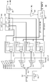
도 5는 본 발명의 일 실시예에 따른 직/병렬 변환 송수신기일 수 있으며 예를 들어 USB 장치(500)에서 사용하기 위한 것인 예시적 송수신기(502)의 적어도 일부를 도시하는 블록도이다. 전술한 바와 같이, 특히 장치(500)가 슬립 모드에 있는 동안에 장치에서 전력 소비를 줄이기 위해서는, 송수신기(502)는 상태 기계(506)나 대안적 제어기 및 상태 기계에 동작가능하게 접속된 다중화기(508)나 대안적 스위칭 회로를 포함하는 대역 외 신호 발생기(504)를 포함한다.FIG. 5 is a block diagram illustrating at least a portion of an
바람직하게는, 상태 기계(506)는 심지어 나머지 송수신기(502)가 비활성 상태(예를 들어, 파워가 꺼지거나, 슬립 중이거나, 전력 공급 중단되는 등의 모드)에 있는 동안에도 활성화되며(예를 들어, 파워가 켜지거나, "깨어 난" 모드 등) 동작가능하며, 예를 들어, CMU(514), 수신기(RX; 516), 송신기 클록 경로(TX Clk 경로) 회로(518), 및 송신기 데이터 경로(TX 데이터 경로) 회로(520)를 포함하는 나머지 송수신기 회로에는 모두 전력 공급이 중단된다. 송신기 데이터 경로 회로(520)는 입력 데이터 워드(tx_word)를 수신하며 직렬 출력 데이터 스트림(tx_data)를 발생시키도록 동작하는 기능 블록(예를 들어, 병렬-직렬 변환기, 전강조 회로, 데이터 리타임 회로 등)을 포함한다. 송신기 클록 경로 회로(518)는 바람직하게 송신기 데이터 경로 회로(520)에서 하나 이상의 기능 블록을 제어하기 위한 클록 및/또는 다른 타이밍/제어 신호를 발생하도록 동작하는 기능 블록(예를 들어, SSC 클록 발생기, 다중화기, 슬루 제어 회로 등)을 포함한다.Preferably,
"SEND_PING" 제어 신호가 장치(500) 내의 링크층(510)으로부터 송수신기(502)로 전송될 때, 바람직하게는 비교적 적은 양의 전력(예를 들어, 수십 마이크로 암페어)을 소비하도록 되어있는 상태 기계(506)가 "SEND_PING" 신호를 감지하며 핑 메시지를 해당 호스트 장치에 전송하기 위해 필요한 최소한의 회로(예를 들어, 송신기(TX) 드라이버(512))에 전력을 공급하도록(즉, 활성화되도록) 동작한다. 링크층(510)에 의해 발생되며 상태 기계(506)로 전송된 SEND_PING 신호는 송수신기가 호스트 장치에 핑 메시지를 전송하고자 하는(그에 의해 그 존재를 브로드캐스팅하는) 요청을 나타낸다.When a "SEND_PING" control signal is sent from the
핑 메시지는 특히 장치가 대기나 슬립 모드에 있는 동안에(즉, 데이터가 장치와 그 해당 호스트 사이에서 전송되지 않는 때에) 접속된 장치의 계속된 존재를 브로드캐스트하기 위해서 호스트 장치에 주기적으로 전송되기 때문에, SEND_PING 신호도 또한 주기적으로 상태 기계(506)에 전송된다. 대안적으로, 본 발명의 다른 실시예에 따르면, SEND_PING 신호는 예를 들어 송수신기(502)에 포함된 타이머나 다른 저전력 타이밍 회로(명시적으로 도시되지 않음)에 의해 내부적으로 발생될 수 있다.Ping messages are sent periodically to the host device to broadcast the continued presence of the attached device, especially while the device is in standby or sleep mode (i.e., when data is not transferred between the device and its host). The SEND_PING signal is also periodically sent to the
상태 기계(506)가 링크층(510)으로부터 비동기 SEND_PING 제어 신호를 감지할 때, 메시지는 외부 클록 소스에 의해 상태 기계로 공급된 외부 기준 클록과 동기화된다. 이러한 방식으로, 통상적으로 장치에서 많은 전력을 소비하는 CMU(514)는 비활성화되어있다(즉, 전력을 끊거나, 전력공급을 중단하는 등). SEND PING 신호가 감지될 때, 상태 기계(506)는 다중화기(508)와 송신기 드라이버(512)를 활성화시키는(예를 들어, 전력을 공급하는) 신호에 대응해서 전력 공급 제어 신호(sm_pu)를 발생시킨다. 바람직하게는, 상태 기계(506)에 의해 발생된 전력 공급 신호는 기능 OR 회로(522; 예를 들어, OR 게이트)의 제 1 입력에 공급된다. OR 게이트(522)의 제 2 입력은 송신기 클록 경로 회로(518)에 의해 발생된 송신기 전력 공급 신호(tx_pu)를 수신하도록 되어있다. 따라서, OR 게이트(522)는 전력 공급 제어 신호(pu_ctl)를 발생시키도록 동작하며, 이 신호는 상태 기계(506)에 의해 발생된 전력 공급 신호(sm_pu) 및/또는 송신기 클로 경로 회로(518)에 의해 발생된 전력 공급 신호(tx_pu)의 함수로서 다중화기와 송신기 드라이버를 선택적으로 활성화하기 위한 다중화기(508)와 송신기 드라이버(512)의 개별적인 제어 (인에이블) 입력에 공급된다.When the
상태 기계(506)는 그 후 데이터 신호(sm_data)를 발생시키며, 그 신호는 바람직하게는 예를 들면 상태 기계에 포함된 토글(T) 플립 플롭(명시적으로 도시되지 않음)이나 대안적 신호 생성기 회로를 토글시킴을 통해서 규정된 개수(예를 들어, 두 개)의 사이클의 기준 클록(즉, 핑 클록)을 포함한다. 본 발명은 SEND_PING 신호에 대응해서 상태 기계(506)에 의해 발생된 특정 개수의 사이클의 기준 클록에 한정되지 않는다는 것이 이해되어야 한다. 더욱이, 상태 기계(506)에 의해 발생된 sm_data 메시지 신호 내의 사이클의 개수는 바람직하게는 SEND_PING 신호의 선언의 존속기간(예를 들어, 선언으로부터 SEND_PING 신호의 선언 중단까지의 기간)과 독립적이다. 토글 플립 플롭은 당업자에게 공지되어 있다. 상태 기계 데이터 신호(sm_data)는 다중화기(508)를 거쳐서 송신기 드라이버(512)로 공급된다(sm_data는 다중화기(508)의 제 1 입력("1")으로 공급된다. 다중화기(508)는 또한 그 제 2 입력("0")에서 송신기 데이터 경로 회로(520)에 의해 발생된 송신기 데이터 신호(tx_data)를 수신하도록 동작한다.The
다중화기(508)는 활성화를 위해서 상태 기계 전력공급 제어 신호(sm_pu)를 사용할 뿐만 아니라, 오히려 다중화기 입력 데이터 경로가 또한 sm_pu에 의해 선택된다. 특히, 상태 기계 전력공급 제어 신호(sm_pu)는 바람직하게는 다중화기(508)의 선택 제어 입력(SEL)에 직접 공급된다. sm_pu가 선언될 때(예를 들어, 논리 "1"일 때), 상태 기계 데이터(sm_data)가 다중화기(508)를 통해 송신기 드라이버(512)에 전송된다. 대안적으로, sm_pu가 선언이 중단될 때(예를 들어, 논리 "0"일 때), 송신기 데이터 경로(520)로부터의 송신기 데이터(tx_data)는 다중화기(508)를 통해 송신기 드라이버9512)로 전송된다. 이러한 방식으로, 다중화기와 드라이버에 공급된 전력공급 제어 신호(pu_ctl)가 선언된다고 가정하면, 다중화기(508)는 송신기 드라이버(512)로의 출력을 위해, 송신기(502)의 동작 모드(예를 들어, 기상이나 슬립 모드)에 따라서 상태 기계 데이터 신호(sm_data)나 송신기 데이터 신호(tx_data) 중 어느 것을 선택하도록 동작한다.The
송신기 드라이버(512)가 두 사이클 핑 클록을 전송한 후에 SEND_PING 신호의 선언이 중단된다. 이 동작은 상태 기계(506)가 전력공급 제어 신호(sm_pu)에 대한 선언을 중단하도록 하며, 그에 의해 다중화기(508)과 송신기 드라이버(512)에 대한 전력공급을 중단한다. 전술한 바와 같이, 다중화기(508)와 송신기 드라이버(512)는 도한 송신기 클록 경로 회로(518)에 의해 발생된 tx_pu 신호의 함수로서 pu_ctl에 의해 독립적으로 전력공급이 될 수 있다. sm_pu 제어 신호에 대한 선언이 중단된다고 가정하면, 다중화기(508)와 송신기 드라이버(512)는 또한 tx_pu 제어 신호의 선언 중단에 의해 전력공급이 중단될 수 있다. sm_pu 제어 신호는 바람직하게 저전력 모드일 수 있는 송신기(502)의 제 1 동작 모드에서 사용되며, tx_pu는 송수신기(502)에 전력이 공급되는 (즉, 활성화되는) 정상(즉, 정규) 모드일 수 있는 제 2 동작 모드에서 사용된다. Declaration of the SEND_PING signal is stopped after the
링크층((510)은 또한 SEND_LFPS 제어 신호를 상태 기계(506)에 전송할 수 있으며, SEND_LFPS 신호는 장치(500) 내의 송수신기(502)가 LFPS 메시지를 호스트 장치에 전송하고자 하는 요청을 나타낸다. 비동기적인 SEND_LFPS 신호는 바람직하게는 상태 기계(506)에 의한 외부 기준 클록과 동기화된다. USB 3.0 사양(예를 들어, "유니버설 시리얼 버스 3.0 사양(Universal Serial Bus 3.0 Specification), 개정 1.0, 섹션 6.9, 페이지 6-30에서 6-35 참조, 그 개시된 내용은 전체적으로 본 명세서에 참조로서 통합된다)에 따르면, LFPS가 저전력 링크 상태에 있는 링크를 가로질러 두 개의 포트 사이에서 측파대 통신을 위해 사용된다. 수신기 종단이 존재하지만 시그널링이 링크에서 발생하지 않는다면, 장치는 전기적으로 유휴 상태에 있는 것으로 간주된다(도 4 참조). 이 상태에 있을 때에, LFPS가 개시 및 전력 관리 정보를 시그널링하기 위해 사용된다.The
SEMD_LFPS 제어 신호를 감지할 때, 상태 기계(506)는 전력공급 신호(sm_pu)를 선언함에 의해서 다중화기(508)와 송신기 드라이버(512)에 전력을 공급한다. 상태 기계(506)는 이후 신호(SEND_LFPS)에 대한 선언을 중지할 때까지 그때 외부 클록 소스로부터 (예를 들어, 상태 기계에서 T 플립 플롭을 토글링함을 통해서) 연속 사이클의 기준 클록을 전송하기 시작한다. 따라서, 상태 기계(506)에 의해 발생된 sm_data 메시지 신호에서 클록 사이클의 수는 SEND_LFPS 신호의 선언의 지속기간의 함수가 될 것이다. 제어 신호 SEND_LFPS에 대한 선언이 중지된 후에(즉, 제거된 후에), 상태 기계(506)는 다중화기(508)와 송신기 드라이버(512)에 대한 전력공급을 중지하며, 상태 기계를 제외한 전체 직/병렬 변환 송수신기(502)는 활성 (즉, 전력공급 중지) 모드로 복귀한다.Upon detecting the SEMD_LFPS control signal, the
도 6은 본 발명의 일 실시예에 따른 도 5에 도시된 예시적 직/병렬 변환 송수신기(502)에서 사용하기에 적합한 예시적인 상태 기계에 의해 수행되는 동작의 적어도 일부를 도시하는 상태 다이어그램(600)이다. 도면에서 명백한 바와 같이, 제 1 상태(S0; 602)에서, 상태 기계는 "유휴" 모드에서 동작하며, 거기에서 상태 기계는 장치 내의 링크층(예를 들어, 도 5에서 510)으로부터 전송된 SEND_PING 신호나 SEND_LFPS 제어 신호를 기다린다. 송신기 클록 경로 회로(예를 들어, 도 5에서 518)가 저전력 모드에 유지된다고 가정하면, 다중화기와 송신기 드라이버(예를 들어, 도 5에서 각각 508과 512)가 둘 다 비활성화되도록(즉, 전력공급이 중지되도록) 상태 기계 전력공급 신호(sm_pu)가 선언이 중단된 상태에 남아있어서, 그에 의해 tx_pu 신호가 선언이 중지된 상태에서 유지된다.FIG. 6 is a state diagram 600 illustrating at least some of the operations performed by an example state machine suitable for use in the example serial /
SEND_PING 제어 신호가 선언될 때, 상태 기계는 유휴 상태(602)에서 제 2 상태(S1; 604)로 전이한다. 상태(604)에서, 상태 기계는 전력공급 제어 신호(sm_pu)를 선언하며, 그에 의해 다중화기와 송신기 드라이버(도 5에서 각각 508과 512)를 활성화시킨다(즉, 전력을 공급한다). 전술한 바와 같이, 논리 "1"인 sm_pu 신호는 또한 상태 기계로부터 수신한 데이터(sm_data)를 전송하기 위해 신호 발생기(도 5에서 504)를 구성하기 위해 다중화기에 있는 상태 기계 데이터 경로를 선택한다. 그때 상태 기계는 호스트 제어기로의 전송을 위해서 두 사이클 핑 메시지나 대안적 대역 외 메시지를 상태 기계 데이터 신호(sm_data)를 통해 송신기 드라이버(도 5에서 512)로 (다중화기를 경유해서) 전송한다. 전술한 바와 같이, 본 발명은 핑 메시지에서 어떤 특정 개수의 사이클에 한정되지 않으며, 더욱이 바람직하게는 SEND_PING 제어 신호가 선언이되는 상태로 남아있는 지속기간에 독립적이다. 핑 메시지의 완료 후에, sm_pu 신호에 대한 선언이 중지되며(예를 들어, 논리 "0"), 그에 의해 다중화기와 송신기 드라이버에 전력이 공급된다. 그때 상태 기계는 유휴 상태(602)로 복귀한다.When the SEND_PING control signal is declared, the state machine transitions from the
대안적으로, SEND_LFPS 제어 신호가 선언될 때, 상태 기계는 유휴 상태(602)에서 세 번째 상태(S2; 606)로 전이한다. 상태(606)에서, 상태 기계는 전력공급 제어 신호(sm_pu)를 선언하며, 그에 의해 다중화기와 송신기 드라이버(도 5에서 각각 508과 512)에 전력을 공급한다. 전술한 바와 같이, 논리 "1"인 sm_pu 신호는 또한 다중화기에 있는 상태 기계 데이터 경로를 선택한다. 그때 상태 기계는 호스트 제어기로의 전송을 위해서 LEPS 메시지를 나타내는 기준 클록의 연속 버스트나 대안적 대역 외 메시지를 sm_data 상에서 송신기 드라이버(예를 들어, 512)로 (다중화기를 경유해서) 전송한다. 전술한 바와 같이, 메시지 신호(sm_data)에 있는 클록 버스트가 SEND_LFPS 신호에 대한 선언이 중지될 때까지 송신된다. LFPS 메시지의 완료 후에, sm_pu 신호에 대한 선언이 중지되며, 그에 의해 다중화기와 송신기 드라이버에 전력이 공급된다. 그때 상태 기계는 유휴 상태(602)로 복귀한다.Alternatively, when the SEND_LFPS control signal is declared, the state machine transitions from an
본 발명의 실시예의 방법론은 예를 들어 휴대용 전자 장치와 같은 전자 장치나 대안적 시스템에서의 구현을 위해 특히 매우 적합하다. 단지 도시를 위해서, 도 7은 본 발명의 일 양태에 따라 형성된 예시적 데이터 처리 시스템(700)을 도시하는 블록도이다. 시스템(700)은 예를 들어 직렬 통신 프로토콜을 사용해서 호스트 장치와 통신하기에 적합하도록 되어있는 이동 장치(예를 들어, USB 장치, SATA 장치, SAS 장치 등)를 나타낼 수 있다. 시스템(700)은 프로세서(702), 메모리(704) 뿐만 아니라 프로세스와 인터페이스하도록 동작하는 입/출력 (I/O) 회로(708)를 포함할 수 있다. 프로세서(702), 메모리(704) 및 I/O 회로(708)는 예를 들어 버스(706)나 대안적 접속 수단을 통해서 데이터 처리 시스템(700)의 일부로서 서로 접속될 수 있다. 예를 들어 버스를 통한 적절한 상호 접속은 또한 컴퓨터 네트워크와 인터페이스하도록 제공될 수 있는 네트워크 인터페이스 카드(NIC)과 같은 네트워크 인터페이스(710), 및 미디어와 인터페이스하도록 제공될 수 있는 디스켓이나 CD-ROM 드라이브와 같은 미디어 인터페이스에 제공될 수 있다. 프로세서(702)는 여기에서 이미 기술된 본 발명의 방법론의 적어도 일부를 수행하도록 구성될 수 있다.The methodology of the embodiments of the present invention is particularly well suited for implementation in alternative systems or electronic devices, for example portable electronic devices. For illustration purposes only, FIG. 7 is a block diagram illustrating an example
여기에서 사용되는 바와 같은 용어 "프로세서"는 예를 들어 중앙처리장치(CPU) 및/또는 다른 처리 회로(예를 들어, 네트워크 프로세서, DSP, 마이크로프로세서 등)를 포함하는 것과 같은 어떤 처리 장치를 포함하도록 의도된다. 추가적으로, 용어 "프로세서"는 하나 이상의 처리 장치를 지칭할 수 있으며 처리 장치와 연관된 다양한 구성요소들이 다른 처리 장치에 의해서 공유될 수 있다는 것이 이해되어야 한다. 여기에서 사용되는 바와 같은 용어 "메모리"는 예를 들어 RAM, ROM, 고정된 저장 매체(예를 들어, 하드 드라이브), 이동 저장 매체(예를 들어, 디스켓), 플래시 메모리 등과 같은 메모리와 프로세서나 CPU와 연관된 다른 컴퓨터 판독가능 매체를 포함하도록 의도된다. 또한, 여기에서 사용된 바와 같은 용어 "I/O 회로"는 예를 들어 데이터를 프로세서에 입력하기 위한 하나 이상의 입력 장치(예를 들어, 키보드, 마우스 등), 프로세서와 관련된 결과들을 제시하기 위한 하나 이상의 출력 장치(예를 들어, 프린터, 모니터 등), 및/또는 입력이나 출력 장치를 프로세스에 동작가능하게 접속하기 위한 인터페이스 회로를 포함하도록 의도된다.The term "processor" as used herein includes any processing device, such as including a central processing unit (CPU) and / or other processing circuitry (eg, network processor, DSP, microprocessor, etc.). Intended to. In addition, it is to be understood that the term “processor” may refer to one or more processing devices and that various components associated with the processing devices may be shared by other processing devices. The term "memory" as used herein refers to memory and processors such as, for example, RAM, ROM, fixed storage media (e.g., hard drives), removable storage media (e.g., diskettes), flash memory, or the like. It is intended to include other computer readable media associated with the CPU. In addition, the term “I / O circuitry” as used herein refers to one or more input devices (eg, a keyboard, a mouse, etc.) for inputting data to the processor, for example, one for presenting results associated with the processor. It is intended to include the above output devices (e.g., printers, monitors, etc.), and / or interface circuits for operatively connecting input or output devices to the process.
따라서, 여기에서 기술된 바와 같은 본 발명의 방법론을 수행하기 위한 명령어나 코드를 포함하는 애플리케이션 프로그램이나 그 소프트웨어 컴포넌트는 하나 이상의 관련 저장 매체(예를 들어, ROM, 고정 또는 이동 저장소)에 저장될 수 있으며, 사용될 준비가 될 때, 프로세서(702)에 의해서 전체적으로 또는 부분적으로 (예를 들어, RAM로) 로딩되어 실행된다. 어느 경우에나, 도 1에 도시된 구성요소들의 적어도 일부는 예를 들어 관련 메모리를 가진 하나 이상의 DSP, ASIC, 기능 회로, 관련 메모리를 가진 하나 이상의 동작가능하게 프로그램된 범용 디지털 컴퓨터 등과 같은 다양한 형태의 하드웨어, 소프트웨어 또는 그 조합으로 구현될 수 있다. 여기에 제공된 본 발명의 개시가 주어진다면, 당업자는 본 발명의 구성요소의 다른 구현을 생각해 낼 수 있을 것이다.Thus, an application program or software component thereof that includes instructions or code for carrying out the methodology of the present invention as described herein may be stored in one or more related storage media (eg, ROM, fixed or removable storage). And, when ready to be used, is loaded and executed in whole or in part (eg, into RAM) by the
본 발명의 개시의 적어도 일부분은 하나 이상의 집적 회로에 구현될 수 있다. 집적 회로를 형성함에 있어서, 다이는 전형적으로 반도체 웨이퍼의 표면에 반복 패턴으로 만들어진다. 각각의 다이는 여기에 기술된 메모리를 포함하며, 다른 구조와 회로를 포함할 수 있다. 개별적인 다이는 웨이퍼로부터 절단되거나 잘라져서 그 후 집적회로로 패키징된다. 당업자는 웨이퍼를 자르는 방법과 집적 회로를 만들기 위해 다이를 패키징하는 방법을 알 것이다. 그렇게 제조된 집적 회로는 본 발명의 일부로 간주될 것이다.At least a portion of the disclosure of the present invention may be implemented in one or more integrated circuits. In forming an integrated circuit, a die is typically made in a repeating pattern on the surface of a semiconductor wafer. Each die includes the memory described herein and may include other structures and circuits. Individual dies are cut or cut from the wafer and then packaged into integrated circuits. Those skilled in the art will know how to cut a wafer and how to package a die to make an integrated circuit. Integrated circuits so manufactured will be considered part of the present invention.
본 발명의 실시예에 따른 집적 회로는 메모리(예를 들어, 내장 또는 별도 메모리)를 사용하는 어느 애플리케이션 및/또는 전자 시스템에서 사용될 수 있다. 본 발명의 실시예를 구현하기 위한 적절한 시스템은 개인용 컴퓨터, 통신 네트워크, 전자 상거래 시스템, 휴대용 통신 장치(예를 들어, 셀룰러 폰), 고체 상태 매체 저장 장치 등을 포함하지만 그에 한정되지는 않는다. 그러한 집적 회로를 포함하는 시스템은 본 발명의 일부로 간주된다. 여기에 제공된 본 발명의 개시가 주어진다면, 당업자는 본 발명의 다른 구현과 애플리케이션을 생각해 낼 수 있을 것이다.Integrated circuits according to embodiments of the present invention may be used in any application and / or electronic system that uses memory (eg, embedded or separate memory). Suitable systems for implementing embodiments of the invention include, but are not limited to, personal computers, communication networks, electronic commerce systems, portable communication devices (eg, cellular phones), solid state media storage devices, and the like. Systems including such integrated circuits are considered part of the present invention. Given the disclosure of the invention provided herein, one of ordinary skill in the art would be able to contemplate other implementations and applications of the invention.
본 발명의 도시적 실시예들이 도면을 참조하여 여기에서 설명되었지만, 본 발명은 그 정확한 실시예에 한정되지 않으며 다양한 변경과 수정이 첨부된 특허청구범위의 범위를 벗어나지 않으면서 당업자에 의해 이루어질 수 있다는 것이 이해되어야 한다.
While illustrative embodiments of the invention have been described herein with reference to the drawings, the invention is not limited to the exact embodiments thereof and that various changes and modifications may be made by those skilled in the art without departing from the scope of the appended claims. Should be understood.
206: 수신
210: 송신
216: 교류 커플링 종단
220: 전치증폭/아날로그 등화기
222: 신호 손실 및 대역 외 감지기
224: 결정 피드백 등화기 및 가산기
226: 고속 래치
228: NCO 클록 위상 회전기
230: 역다중화기 및 바이트 정렬기
232: 루프 필터 및 회전 주파수 분할기
234: 결정 피드백 등화기 및 전치증폭 적응
235: 수신 전압 조정기
236: 마스터 위상동기 루프
238: CMU 전압 조정기
240: 바이어스 발생기
242: FIFO
244: 병렬-직렬
248: NCO 확산 스펙트럼 클록킹
250: 2-탭 전강조
254: 진폭, 슬루 및 OOB 제어
256: 송신 드라이버206: Receive
210: transmit
216: AC coupling termination
220: preamplifier / analog equalizer
222: signal loss and out-of-band detector
224: decision feedback equalizer and adder
226: high speed latch
228: NCO Clock Phase Rotator
230: demultiplexer and byte sorter
232: loop filter and rotation frequency divider
234: Adaptation of decision feedback equalizers and preamplification
235: receive voltage regulator
236: master phase-locked loop
238: CMU voltage regulator
240: bias generator
242: FIFO
244: parallel-serial
248: NCO spread spectrum clocking
250: 2-tap full emphasis
254: Amplitude, Slew, and OOB Control
256: Send driver
Claims (23)
스위칭 회로와,
상기 스위칭 회로에 접속되는 제어기를 포함하되, 상기 제어기는 기준 클록 신호를 수신하고, 상기 제 1 장치가 제 1 동작 모드에 있을 때 상기 제 1 장치가 메시지를 상기 제 2 장치에 보내고자 하는 요청을 나타내는 적어도 제 1 제어 신호를 수신하며, 출력 제어 신호와 출력 데이터 신호를 발생시키도록 동작하되, 상기 출력 제어 신호는 상기 제 1 모드 중에 상기 스위칭 회로와 상기 제 1 장치의 송신기 드라이버에 선택적으로 전력을 공급하기 위해 상기 적어도 제 1 제어 신호의 함수로서 동작하며, 상기 출력 데이터 신호는 상기 제 1 모드 중에 상기 제 2 장치로의 전송을 위해 상기 스위칭 회로를 통해 상기 송신기 드라이버로 공급된 상기 메시지를 포함하는
신호 생성기 회로.
A signal generator circuit for reducing power consumption of message communication between a first device having a signal generator circuit and a second device in communication with the first device, the method comprising:
With a switching circuit,
A controller coupled to the switching circuit, the controller receiving a reference clock signal and requesting the first device to send a message to the second device when the first device is in a first mode of operation. Receive at least a first control signal, wherein the output control signal is configured to generate an output control signal and an output data signal, the output control signal selectively powering the switching circuit and the transmitter driver of the first device during the first mode. Operating as a function of the at least first control signal to supply, the output data signal comprising the message supplied to the transmitter driver through the switching circuit for transmission to the second device during the first mode.
Signal generator circuit.
상기 제 1 모드 중에 상기 제 1 제어 신호가 선언(assert)될 때, 상기 제어기는 상기 스위칭 회로와 상기 송신기 드라이버에 전력을 공급하며, 상기 제 1 모드 중에 상기 제 1 제어 신호의 선언이 중지될 때, 상기 제어기는 상기 스위칭 회로와 상기 송신기 드라이버에 대한 전력 공급을 끊도록 동작하는
신호 생성기 회로.
The method of claim 1,
When the first control signal is asserted during the first mode, the controller supplies power to the switching circuit and the transmitter driver, and when the declaration of the first control signal is stopped during the first mode. The controller is operative to disconnect power to the switching circuit and the transmitter driver.
Signal generator circuit.
상기 제어기는 또한 제 2 제어 신호를 수신하도록 동작하고, 상기 제 1 제어 신호는 상기 제 1 모드 중에 상기 제 2 장치에 핑 메시지를 전송하는 요청을 나타내며, 상기 제 2 제어 신호는 상기 제 1 모드 중에 저주파 주기 시그널링(low frequency periodic signaling, LFPS) 메시지를 상기 제 2 장치에 전송하는 요청을 나타내는
신호 생성기 회로.
The method of claim 1,
The controller is further operative to receive a second control signal, the first control signal indicating a request to send a ping message to the second device during the first mode, wherein the second control signal is transmitted during the first mode. Represents a request to send a low frequency periodic signaling (LFPS) message to the second device
Signal generator circuit.
상기 제 1 제어 신호가 선언될 때, 상기 제어기에 의해서 발생되는 상기 출력 데이터 신호는 규정된 개수의 사이클의 상기 기준 클록을 포함하며, 상기 제 2 제어 신호가 선언될 때, 상기 출력 데이터 신호는 상기 제 2 제어 신호의 선언이 중지될 때까지 연속된 사이클의 상기 기준 클록을 발생시키도록 동작하는
신호 생성기 회로.
The method of claim 3, wherein
When the first control signal is declared, the output data signal generated by the controller includes the reference clock of a defined number of cycles, and when the second control signal is declared, the output data signal is generated by the Operative to generate the reference clock in successive cycles until the declaration of the second control signal is stopped
Signal generator circuit.
상기 제 1 제어 신호가 선언될 때, 상기 제어기에 의해 발생된 상기 출력 데이터 신호는 상기 제 1 제어 신호의 선언의 지속기간에 독립적으로 일정한 개수의 사이클의 상기 기준 클록을 포함하며, 상기 제 2 제어 신호가 선언될 때, 상기 출력 데이터 신호는 상기 제 2 제어 신호의 선언의 지속기간에 의존하는 일정한 개수의 사이클의 상기 기준 클록을 포함하는
신호 생성기 회로.
The method of claim 3, wherein
When the first control signal is declared, the output data signal generated by the controller includes a certain number of cycles of the reference clock independently of the duration of the declaration of the first control signal, wherein the second control When the signal is declared, the output data signal includes a certain number of cycles of the reference clock depending on the duration of the declaration of the second control signal.
Signal generator circuit.
상기 스위칭 회로는 상기 제어기에 의해 발생된 상기 출력 데이터 신호를 수신하기 위한 제 1 입력, 상기 제 1 장치가 제 2 동작 모드에 있을 때 상기 제 1 장치에 있는 송신기 데이터 경로 회로에 의해 발생된 출력 데이터 스트림을 수신하기 위한 제 2 입력, 및 상기 출력 데이터 신호와 상기 출력 데이터 스트림 중 하나를 상기 스위칭 회로에 공급되는 선택 신호의 함수로서 상기 송신기 드라이버에 선택적으로 전달하는 출력부를 포함하는
신호 생성기 회로.The method of claim 1,
The switching circuit is a first input for receiving the output data signal generated by the controller, output data generated by a transmitter data path circuit in the first device when the first device is in a second mode of operation. A second input for receiving a stream and an output for selectively passing one of the output data signal and the output data stream to the transmitter driver as a function of a selection signal supplied to the switching circuit;
Signal generator circuit.
상기 스위칭 회로에 공급되는 상기 선택 신호는 상기 제어기에 의해 발생된 상기 출력 제어 신호인
신호 생성기 회로.
The method according to claim 6,
The selection signal supplied to the switching circuit is the output control signal generated by the controller.
Signal generator circuit.
상기 제어기에 의해 발생된 상기 출력 제어 신호를 수신하기 위한 제 1 입력, 상기 제 1 장치의 제 2 동작 모드 중에 상기 송신기 클록 경로 회로에 의해서 발생된 전력공급 신호를 수신하기 위한 제 2 입력, 및 상기 스위칭 회로에 접속되고, 상기 송신기 드라이버에 접속되도록 되어 있으며, 상기 제어기에 의해 발생된 상기 출력 제어 신호와 상기 송신기 클록 경로 회로에 의해 발생된 상기 전력공급 신호 중 적어도 하나의 함수로서 상기 스위칭 회로와 상기 송신기 드라이버에 선택적으로 전력을 공급하기 위한 제어 신호를 발생시키도록 동작하는 출력을 포함하는 기능 OR 회로를 더 포함하는
신호 생성기 회로.
The method of claim 1,
A first input for receiving the output control signal generated by the controller, a second input for receiving a power supply signal generated by the transmitter clock path circuit during a second mode of operation of the first device, and the A switching circuit and adapted to be connected to the transmitter driver and as a function of at least one of the output control signal generated by the controller and the power supply signal generated by the transmitter clock path circuit. Further comprising a functional OR circuit including an output operative to generate a control signal for selectively powering a transmitter driver
Signal generator circuit.
상기 제 1 장치에 있는 송신기 데이터 경로 회로, 송신기 클록 경로 회로 및 클록 증배기 유닛 중 적어도 하나는 상기 제 1 모드 중에 전력이 공급되는 상태로 유지되는
신호 생성기 회로.
The method of claim 1,
At least one of a transmitter data path circuit, a transmitter clock path circuit, and a clock multiplier unit in the first device are maintained powered during the first mode.
Signal generator circuit.
상기 제어기는 적어도 하나의 상태 기계(state machine)를 포함하는
신호 생성기 회로.
The method of claim 1,
The controller includes at least one state machine
Signal generator circuit.
상기 스위칭 회로는 다중화기를 포함하는
신호 생성기 회로.
The method of claim 1,
The switching circuit comprises a multiplexer
Signal generator circuit.
상기 제 1 동작 모드는 상기 제 1 장치의 전력공급 중단 모드이며, 상기 제 2 동작 모드는 상기 제 1 장치의 활성 모드인
신호 생성기 회로.The method of claim 1,
The first operation mode is a power supply interruption mode of the first device, and the second operation mode is an active mode of the first device.
Signal generator circuit.
상기 제 1 장치가 상기 제 2 장치로 메시지를 전송하고자 하는 요청을 나타내는 상기 제 1 제어 신호는 상기 제 1 장치에 있는 링크층에 의해 발생되는
신호 생성기 회로.
The method of claim 1,
The first control signal indicative of a request for the first device to send a message to the second device is generated by a link layer at the first device.
Signal generator circuit.
집적 회로.
At least one signal generator circuit according to claim 1
integrated circuit.
입력 데이터 워드를 수신하며 출력 데이터 스트림을 생성하도록 동작하는 데이터 경로 회로와, 상기 입력 데이터 워드의 처리를 제어하기 위한 적어도 하나의 제어 신호를 발생시키도록 동작하는 클록 경로 회로와, 상기 호스트 장치에 상기 출력 데이터 스트림을 전송하도록 동작하는 드라이버를 포함하는 송신기와,
상기 송신기 내의 상기 클록 경로 회로에 의해서 사용되기 위한 적어도 하나의 타이밍 신호를 발생시키도록 동작하는 클록 증배 유닛과,
신호 생성기 회로를 포함하며,
상기 신호 생성기 회로는
스위칭 회로와,
상기 스위칭 회로에 접속되는 제어기를 포함하되, 상기 제어기는 기준 클록 신호를 수신하고, 상기 직렬 장치가 제 1 동작 모드에 있을 때 상기 직렬 장치가 메시지를 상기 호스트 장치에 보내고자 하는 요청을 나타내는 적어도 제 1 제어 신호를 수신하며, 출력 제어 신호와 출력 데이터 신호를 발생시키도록 동작하되, 상기 출력 제어 신호는 상기 제 1 모드 중에 상기 스위칭 회로와 상기 직렬 장치의 송신기 드라이버에 선택적으로 전력을 공급하기 위해서 상기 적어도 제 1 제어 신호의 함수로서 동작하며, 상기 출력 데이터 신호는 상기 제 1 모드 중에 상기 호스트 장치로의 전송을 위해서 상기 스위칭 회로를 통해 상기 송신기 드라이버로 공급된 상기 메시지를 포함하는
직렬 장치.
A serial device having a reduced power consumption for message communication between a serial device and a host device in communication with the serial device, the method comprising:
A data path circuit operative to receive an input data word and to generate an output data stream, a clock path circuit operative to generate at least one control signal for controlling the processing of the input data word; A transmitter comprising a driver operative to transmit an output data stream;
A clock multiplication unit operative to generate at least one timing signal for use by the clock path circuit in the transmitter;
A signal generator circuit,
The signal generator circuit
With a switching circuit,
A controller coupled to the switching circuit, the controller receiving at least a reference clock signal and indicating at least one request indicating that the serial device sends a message to the host device when the serial device is in a first mode of operation. Receive a control signal and generate an output control signal and an output data signal, the output control signal being configured to selectively power the switching circuit and the transmitter driver of the serial device during the first mode. Operating as a function of at least a first control signal, the output data signal including the message supplied to the transmitter driver through the switching circuit for transmission to the host device during the first mode.
Serial device.
상기 직렬 장치 내에 있는 상기 송신기 데이터 경로 회로, 상기 송신기 클록 경로 회로 및 상기 클록 증배 유닛 중 적어도 하나는 상기 제 1 모드 중에 전력공급이 중단된 상태로 유지되는
직렬 장치.
The method of claim 15,
At least one of the transmitter data path circuit, the transmitter clock path circuit, and the clock multiplication unit in the serial device remains uninterrupted during the first mode.
Serial device.
상기 제 1 모드 중에 상기 제 1 제어 신호가 선언될 때, 상기 제어기는 상기 스위칭 회로와 상기 송신기 드라이버에 전력을 공급하며, 상기 제 1 모드 중에 상기 제 1 제어 신호의 선언이 중지될 때, 상기 제어기는 상기 스위칭 회로와 상기 송신기 드라이버에 대한 전력 공급을 끊도록 동작하는
직렬 장치.
The method of claim 15,
The controller supplies power to the switching circuit and the transmitter driver when the first control signal is declared during the first mode, and when the declaration of the first control signal is stopped during the first mode. Is operative to disconnect power to the switching circuit and the transmitter driver.
Serial device.
상기 제어기는 또한 제 2 제어 신호를 수신하도록 동작하고, 상기 제 1 제어 신호는 상기 제 1 모드 중에 상기 호스트 장치에 핑 메시지를 전송하는 요청을 나타내며, 상기 제 2 제어 신호는 상기 제 1 모드 중에 저주파 주기 시그널링(low frequency periodic signaling, LFPS) 메시지를 상기 호스트 장치에 전송하는 요청을 나타내는
직렬 장치.
The method of claim 15,
The controller is further operative to receive a second control signal, the first control signal indicating a request to send a ping message to the host device during the first mode, wherein the second control signal is low frequency during the first mode. Indicates a request to send a low frequency periodic signaling (LFPS) message to the host device
Serial device.
상기 제 1 제어 신호가 선언될 때, 상기 제어기에 의해서 발생되는 상기 출력 데이터 신호는 규정된 개수의 사이클의 상기 기준 클록을 포함하며, 상기 제 2 제어 신호가 선언될 때, 상기 출력 데이터 신호는 상기 제 2 제어 신호의 선언이 중지될 때까지 연속된 사이클의 상기 기준 클록을 발생시키도록 동작하는
직렬 장치.
The method of claim 18,
When the first control signal is declared, the output data signal generated by the controller includes the reference clock of a defined number of cycles, and when the second control signal is declared, the output data signal is generated by the Operative to generate the reference clock in successive cycles until the declaration of the second control signal is stopped
Serial device.
상기 제 1 제어 신호가 선언될 때, 상기 제어기에 의해 발생된 상기 출력 데이터 신호는 상기 제 1 제어 신호의 선언의 지속기간에 독립적으로 일정한 개수의 사이클의 상기 기준 클록을 포함하며, 상기 제 2 제어 신호가 선언될 때, 상기 출력 데이터 신호는 상기 제 2 제어 신호의 선언의 지속기간에 의존하는 일정한 개수의 사이클의 상기 기준 클록을 포함하는
직렬 장치.
The method of claim 18,
When the first control signal is declared, the output data signal generated by the controller includes a certain number of cycles of the reference clock independently of the duration of the declaration of the first control signal, wherein the second control When the signal is declared, the output data signal includes a certain number of cycles of the reference clock depending on the duration of the declaration of the second control signal.
Serial device.
상기 스위칭 회로는 상기 제어기에 의해 발생된 상기 출력 데이터 신호를 수신하기 위한 제 1 입력부와, 상기 직렬 장치가 제 2 동작 모드에 있을 때 상기 송신기에 있는 상기 데이터 경로 회로에 의해 발생된 상기 출력 데이터 스트림을 수신하기 위한 제 2 입력부와, 상기 제어기에 의해 발생된 상기 출력 데이터 신호와 상기 데이터 경로 회로에 의해 발생된 상기 출력 데이터 스트림 중 하나를 상기 스위칭 회로에 공급되는 선택 신호의 함수로서 상기 드라이버에 선택적으로 전달하는 출력을 포함하는
직렬 장치.
The method of claim 15,
The switching circuit comprises a first input for receiving the output data signal generated by the controller and the output data stream generated by the data path circuitry in the transmitter when the serial device is in a second mode of operation. A second input for receiving a signal, and one of the output data signal generated by the controller and the output data stream generated by the data path circuit is optional to the driver as a function of a selection signal supplied to the switching circuit Containing the output to pass
Serial device.
상기 제어기에 의해 발생된 상기 출력 제어 신호를 수신하기 위한 제 1 입력부와, 상기 직렬 장치의 제 2 동작 모드 중에 상기 송신기 내에 있는 상기 클록 경로 회로에 의해서 발생된 전력공급 신호를 수신하기 위한 제 2 입력부와, 상기 스위칭 회로에 접속되고, 상기 송신기 내에 있는 상기 드라이버에 접속되도록 되어 있으며, 상기 제어기에 의해 발생된 상기 출력 제어 신호와 상기 클록 경로 회로에 의해 발생된 상기 전력공급 신호 중 적어도 하나의 함수로서 상기 스위칭 회로와 상기 드라이버에 선택적으로 전력을 공급하기 위한 제어 신호를 발생시키도록 동작하는 출력을 포함하는 기능 OR 회로를 더 포함하는
직렬 장치.
The method of claim 21,
A first input for receiving the output control signal generated by the controller and a second input for receiving a power supply signal generated by the clock path circuitry in the transmitter during a second mode of operation of the serial device And to be connected to the switching circuit and to the driver in the transmitter, as a function of at least one of the output control signal generated by the controller and the power supply signal generated by the clock path circuit. Further comprising a functional OR circuit comprising an output operative to generate a control signal for selectively powering the switching circuit and the driver.
Serial device.
기준 클록 신호를 상기 제 1 장치에서 수신하는 단계와,
상기 제 1 장치가 제 1 동작 모드에 있을 때 상기 제 1 장치가 상기 제 2 장치에 메시지를 전송하고자 하는 요청을 나타내는 적어도 제 1 제어 신호를 상기 제 1 장치에서 수신하는 단계와,
출력 제어 신호와 출력 데이터 신호를 상기 제 1 장치에서 생성하는 단계를 포함하되, 상기 출력 제어 신호는 상기 제 1 모드 중에 상기 제 1 장치에서 스위칭 회로와 송신기 드라이버에 선택적으로 전력공급을 하기 위해 상기 적어도 제 1 제어 신호의 함수로서 동작하고, 상기 출력 데이터 신호는 상기 제 1 모드 중에 상기 제 2 장치에 전송하기 위해 상기 스위칭 회로를 통해 상기 송신기 드라이버에 공급되는 상기 메시지를 포함하며, 상기 메시지는 상기 기준 클록 신호에 동기되는
방법.A method for reducing power consumption of message communications between a first device and a second device in communication with the first device, the method comprising:
Receiving a reference clock signal at the first device;
Receiving at the first device at least a first control signal indicating that the first device wants to send a message to the second device when the first device is in a first mode of operation;
Generating an output control signal and an output data signal at the first device, the output control signal being adapted to selectively power the switching circuit and the transmitter driver at the first device during the first mode. Operating as a function of a first control signal, the output data signal includes the message supplied to the transmitter driver through the switching circuit for transmission to the second device during the first mode, the message being the reference Synchronized to the clock signal
Way.
Applications Claiming Priority (2)
| Application Number | Priority Date | Filing Date | Title |
|---|---|---|---|
| US12/790,283 US8713338B2 (en) | 2010-05-28 | 2010-05-28 | Methods and apparatus for low power out-of-band communications |
| US12/790,283 | 2010-05-28 |
Publications (1)
| Publication Number | Publication Date |
|---|---|
| KR20110131129A true KR20110131129A (en) | 2011-12-06 |
Family
ID=44312356
Family Applications (1)
| Application Number | Title | Priority Date | Filing Date |
|---|---|---|---|
| KR1020110050557A KR20110131129A (en) | 2010-05-28 | 2011-05-27 | Methods and apparatus for low power out-of-band communications |
Country Status (6)
| Country | Link |
|---|---|
| US (1) | US8713338B2 (en) |
| EP (1) | EP2390755A1 (en) |
| JP (1) | JP5646394B2 (en) |
| KR (1) | KR20110131129A (en) |
| CN (1) | CN102262435A (en) |
| TW (1) | TW201217956A (en) |
Cited By (1)
| Publication number | Priority date | Publication date | Assignee | Title |
|---|---|---|---|---|
| KR20150076210A (en) * | 2012-12-19 | 2015-07-06 | 인텔 코포레이션 | Re-driver power management |
Families Citing this family (32)
| Publication number | Priority date | Publication date | Assignee | Title |
|---|---|---|---|---|
| US8601302B2 (en) * | 2009-06-22 | 2013-12-03 | Amazon Technologies, Inc. | Processor system in low power state retention mode with linear regulator off and switch regulator low in power management IC |
| US8612786B1 (en) * | 2010-09-24 | 2013-12-17 | Amazon Technologies, Inc. | Deep idle mode |
| US8457247B2 (en) * | 2010-11-18 | 2013-06-04 | Plx Technology, Inc. | In-band generation of low-frequency periodic signaling |
| TWI469004B (en) * | 2011-04-08 | 2015-01-11 | Raydium Semiconductor Corp | Driving and sensing method for touch input device, and module using the same |
| US9648561B2 (en) * | 2011-07-27 | 2017-05-09 | Seagate Technology Llc | Access point device with wakeup mode |
| WO2013048943A1 (en) | 2011-09-30 | 2013-04-04 | Intel Corporation | Active state power management (aspm) to reduce power consumption by pci express components |
| US8705605B1 (en) * | 2011-11-03 | 2014-04-22 | Altera Corporation | Technique for providing loopback testing with single stage equalizer |
| MY178860A (en) | 2011-12-28 | 2020-10-21 | Intel Corp | Power gated communication controller |
| JP5792645B2 (en) * | 2012-01-13 | 2015-10-14 | ルネサスエレクトロニクス株式会社 | Semiconductor device and control method thereof |
| US20140006826A1 (en) * | 2012-06-30 | 2014-01-02 | Mahesh Wagh | Low power low frequency squelch break protocol |
| US8683091B2 (en) * | 2012-06-30 | 2014-03-25 | Intel Corporation | Device disconnect detection |
| US8909815B2 (en) * | 2012-11-07 | 2014-12-09 | Analogix Semiconductor, Inc. | Devices and methods for multiple data streams over USB 2.0 |
| US9507372B2 (en) | 2013-06-21 | 2016-11-29 | Sandisk Technologies Llc | Out-of-band signal detection by host interfaces of storage modules |
| US10042412B2 (en) * | 2014-12-08 | 2018-08-07 | Intel Corporation | Interconnect wake response circuit and method |
| US9455758B1 (en) * | 2015-05-18 | 2016-09-27 | The Regents Of The University Of Michigan | Ultra-low power long range transceiver |
| TWI705666B (en) * | 2015-06-15 | 2020-09-21 | 日商新力股份有限公司 | Transmission device, receiving device, communication system |
| US20170168968A1 (en) * | 2015-12-15 | 2017-06-15 | Qualcomm Incorporated | Audio bus interrupts |
| GB2548144B (en) * | 2016-03-10 | 2021-04-28 | Lasermet Ltd | Two-channel communication systems |
| CN105915637A (en) * | 2016-06-07 | 2016-08-31 | 厦门纳网科技股份有限公司 | Remote automatic standby and awakening method based on storage system server |
| US11436181B2 (en) | 2016-06-30 | 2022-09-06 | Copper Inc. | Data processing systems and methods for transmitting and modifying data via a smart data cable |
| CN109643416A (en) | 2016-06-30 | 2019-04-16 | 科珀有限责任公司 | Intelligent data cable for point of sales system |
| EP3547723B1 (en) * | 2016-12-15 | 2023-02-15 | Huawei Technologies Co., Ltd. | Information transmission method and network element selector |
| DE102017208361A1 (en) * | 2017-05-18 | 2018-11-22 | Robert Bosch Gmbh | sensor device |
| CN111149077A (en) * | 2018-01-25 | 2020-05-12 | 英特尔公司 | Power management for discrete communication port assemblies |
| CN113342592B (en) * | 2020-03-03 | 2023-08-25 | 合肥杰发科技有限公司 | Disconnection detection method, device and medium of hot plug equipment |
| CN112084736B (en) * | 2020-08-17 | 2024-04-05 | 武汉汇迪森信息技术有限公司 | USB3.0 physical layer transceiver based on FPGA |
| US11321693B1 (en) | 2020-12-10 | 2022-05-03 | Copper Inc. | Data processing systems and methods for transmitting and modifying data via a smart data cable |
| US11321261B1 (en) | 2020-12-10 | 2022-05-03 | Copper Inc. | Data processing systems and methods for transmitting and modifying data via a smart data cable |
| CN114826279A (en) * | 2021-01-18 | 2022-07-29 | 瑞昱半导体股份有限公司 | Receive circuit of deserializer |
| US11789807B1 (en) | 2021-03-30 | 2023-10-17 | Amazon Technologies, Inc. | Autonomous management of communication links |
| CN113259005B (en) * | 2021-05-11 | 2023-02-24 | 重庆大学 | Distributed digital pre-equalization system and method |
| US11909850B1 (en) * | 2021-06-23 | 2024-02-20 | Amazon Technologies, Inc. | Dynamic improvement of a communication channel |
Family Cites Families (10)
| Publication number | Priority date | Publication date | Assignee | Title |
|---|---|---|---|---|
| WO1998020609A1 (en) | 1996-11-04 | 1998-05-14 | Advanced Micro Devices, Inc. | Low power wake-up system and method |
| US6567921B1 (en) | 1999-01-25 | 2003-05-20 | Agere Systems, Inc. | Asynchronous low power mode bus controller circuit and method of low power mode operation |
| US6625740B1 (en) * | 2000-01-13 | 2003-09-23 | Cirrus Logic, Inc. | Dynamically activating and deactivating selected circuit blocks of a data processing integrated circuit during execution of instructions according to power code bits appended to selected instructions |
| US7051227B2 (en) * | 2002-09-30 | 2006-05-23 | Intel Corporation | Method and apparatus for reducing clock frequency during low workload periods |
| JP3807406B2 (en) * | 2003-09-05 | 2006-08-09 | セイコーエプソン株式会社 | Data transfer control device and electronic device |
| US7739528B2 (en) | 2006-06-09 | 2010-06-15 | Broadcom Corporation | Method for managing and controlling the low power modes for an integrated circuit device |
| EP2107495B1 (en) * | 2008-04-01 | 2012-09-19 | Assa Abloy Ab | Switched capacitance method for the detection of, and subsequent communication with a wireless transponder device using a single antenna |
| US8078768B2 (en) | 2008-08-21 | 2011-12-13 | Qualcomm Incorporated | Universal Serial Bus (USB) remote wakeup |
| JP5173880B2 (en) * | 2008-10-03 | 2013-04-03 | ルネサスエレクトロニクス株式会社 | Serial data transfer device |
| US8135972B2 (en) * | 2009-03-10 | 2012-03-13 | Cortina Systems, Inc. | Data interface power consumption control |
-
2010
- 2010-05-28 US US12/790,283 patent/US8713338B2/en active Active
-
2011
- 2011-05-23 TW TW100118014A patent/TW201217956A/en unknown
- 2011-05-24 EP EP11167211A patent/EP2390755A1/en not_active Withdrawn
- 2011-05-27 CN CN2011101393413A patent/CN102262435A/en active Pending
- 2011-05-27 KR KR1020110050557A patent/KR20110131129A/en active IP Right Grant
- 2011-05-27 JP JP2011118591A patent/JP5646394B2/en not_active Expired - Fee Related
Cited By (1)
| Publication number | Priority date | Publication date | Assignee | Title |
|---|---|---|---|---|
| KR20150076210A (en) * | 2012-12-19 | 2015-07-06 | 인텔 코포레이션 | Re-driver power management |
Also Published As
| Publication number | Publication date |
|---|---|
| JP5646394B2 (en) | 2014-12-24 |
| US20110296215A1 (en) | 2011-12-01 |
| US8713338B2 (en) | 2014-04-29 |
| EP2390755A1 (en) | 2011-11-30 |
| JP2011248896A (en) | 2011-12-08 |
| TW201217956A (en) | 2012-05-01 |
| CN102262435A (en) | 2011-11-30 |
Similar Documents
| Publication | Publication Date | Title |
|---|---|---|
| KR20110131129A (en) | Methods and apparatus for low power out-of-band communications | |
| US8805196B2 (en) | Electro-optical communications link | |
| US7647517B2 (en) | PCI express system and method of transitioning link state including adjusting threshold idle time according to a requirement of data transmission | |
| US9965018B1 (en) | Power management for PCI express | |
| EP1388975B1 (en) | System and method for data transition control in a multirate communication system | |
| KR20120125572A (en) | Hybrid interface for serial and parallel communication | |
| CN107688550B (en) | Device connection detection | |
| US7463706B2 (en) | System and method for performing on-chip synchronization of system signals utilizing off-chip harmonic signal | |
| US8964905B1 (en) | Low power serial link | |
| WO2000016525A1 (en) | A system and method for sending and receiving data signals over a clock signal line | |
| JP2004520649A (en) | Source synchronous receiver link initialization and input floating control with clock detection and DLL lock detection | |
| TWI811732B (en) | Method of controlling an interface system connectable to a host | |
| US20230106072A1 (en) | Using dynamic bursts to support frequency-agile memory interfaces | |
| WO2024010630A1 (en) | Dynamic spread-spectrum-clocking control | |
| JP2011166502A (en) | Physical layer circuit | |
| WO2002039683A2 (en) | Apparatus and method for sending and receiving data signals over a clock signal line by pulse with modulation | |
| US20200285602A1 (en) | eUSB2 to USB 2.0 Data Transmission with Surplus Sync Bits | |
| US10698439B1 (en) | Efficient clock forwarding scheme | |
| TWI676888B (en) | Systems and methods providing a low-power mode for serial links | |
| JP5780050B2 (en) | Transmission system | |
| Li et al. | A 5 Gb/s multi-mode transmitter with de-emphasis for PCI Express 2.0/USB 3.0 | |
| JP2014033073A (en) | Semiconductor device | |
| JP2005063293A (en) | High speed interface power management system | |
| CN117857001A (en) | MAC controller and data signal transmission method |
Legal Events
| Date | Code | Title | Description |
|---|---|---|---|
| A201 | Request for examination | ||
| E902 | Notification of reason for refusal | ||
| E701 | Decision to grant or registration of patent right |