KR20110090971A - Inverted organic photosensitive devices - Google Patents
Inverted organic photosensitive devices Download PDFInfo
- Publication number
- KR20110090971A KR20110090971A KR1020117012209A KR20117012209A KR20110090971A KR 20110090971 A KR20110090971 A KR 20110090971A KR 1020117012209 A KR1020117012209 A KR 1020117012209A KR 20117012209 A KR20117012209 A KR 20117012209A KR 20110090971 A KR20110090971 A KR 20110090971A
- Authority
- KR
- South Korea
- Prior art keywords
- heterojunction
- donor
- receptor
- organic
- inverting
- Prior art date
Links
- 239000000463 material Substances 0.000 claims description 88
- 229910052751 metal Inorganic materials 0.000 claims description 51
- 239000002184 metal Substances 0.000 claims description 51
- 239000000758 substrate Substances 0.000 claims description 39
- 238000000034 method Methods 0.000 claims description 27
- 230000000903 blocking effect Effects 0.000 claims description 23
- 230000005670 electromagnetic radiation Effects 0.000 claims description 20
- 238000004519 manufacturing process Methods 0.000 claims description 10
- AMGQUBHHOARCQH-UHFFFAOYSA-N indium;oxotin Chemical compound [In].[Sn]=O AMGQUBHHOARCQH-UHFFFAOYSA-N 0.000 claims description 7
- 238000004381 surface treatment Methods 0.000 claims description 7
- RTZYCRSRNSTRGC-LNTINUHCSA-K (z)-4-oxopent-2-en-2-olate;ruthenium(3+) Chemical compound [Ru+3].C\C([O-])=C\C(C)=O.C\C([O-])=C\C(C)=O.C\C([O-])=C\C(C)=O RTZYCRSRNSTRGC-LNTINUHCSA-K 0.000 claims description 6
- XMWRBQBLMFGWIX-UHFFFAOYSA-N C60 fullerene Chemical compound C12=C3C(C4=C56)=C7C8=C5C5=C9C%10=C6C6=C4C1=C1C4=C6C6=C%10C%10=C9C9=C%11C5=C8C5=C8C7=C3C3=C7C2=C1C1=C2C4=C6C4=C%10C6=C9C9=C%11C5=C5C8=C3C3=C7C1=C1C2=C4C6=C2C9=C5C3=C12 XMWRBQBLMFGWIX-UHFFFAOYSA-N 0.000 claims description 6
- 229910003472 fullerene Inorganic materials 0.000 claims description 6
- 150000002739 metals Chemical class 0.000 claims description 6
- TVIVIEFSHFOWTE-UHFFFAOYSA-K tri(quinolin-8-yloxy)alumane Chemical compound [Al+3].C1=CN=C2C([O-])=CC=CC2=C1.C1=CN=C2C([O-])=CC=CC2=C1.C1=CN=C2C([O-])=CC=CC2=C1 TVIVIEFSHFOWTE-UHFFFAOYSA-K 0.000 claims description 6
- GGNDPFHHUHTCIO-UHFFFAOYSA-N 1h-benzimidazole;perylene-3,4,9,10-tetracarboxylic acid Chemical compound C1=CC=C2NC=NC2=C1.C1=CC=C2NC=NC2=C1.C=12C3=CC=C(C(O)=O)C2=C(C(O)=O)C=CC=1C1=CC=C(C(O)=O)C2=C1C3=CC=C2C(=O)O GGNDPFHHUHTCIO-UHFFFAOYSA-N 0.000 claims description 5
- PMJMHCXAGMRGBZ-UHFFFAOYSA-N subphthalocyanine Chemical compound N1C(N=C2C3=CC=CC=C3C(=N3)N2)=C(C=CC=C2)C2=C1N=C1C2=CC=CC=C2C3=N1 PMJMHCXAGMRGBZ-UHFFFAOYSA-N 0.000 claims description 5
- 238000011282 treatment Methods 0.000 claims description 5
- ZSYMVHGRKPBJCQ-UHFFFAOYSA-N 1,1'-biphenyl;9h-carbazole Chemical group C1=CC=CC=C1C1=CC=CC=C1.C1=CC=C2C3=CC=CC=C3NC2=C1 ZSYMVHGRKPBJCQ-UHFFFAOYSA-N 0.000 claims description 4
- XKRFYHLGVUSROY-UHFFFAOYSA-N Argon Chemical compound [Ar] XKRFYHLGVUSROY-UHFFFAOYSA-N 0.000 claims description 4
- GYHNNYVSQQEPJS-UHFFFAOYSA-N Gallium Chemical compound [Ga] GYHNNYVSQQEPJS-UHFFFAOYSA-N 0.000 claims description 4
- CBENFWSGALASAD-UHFFFAOYSA-N Ozone Chemical compound [O-][O+]=O CBENFWSGALASAD-UHFFFAOYSA-N 0.000 claims description 4
- 229910052733 gallium Inorganic materials 0.000 claims description 4
- RBTKNAXYKSUFRK-UHFFFAOYSA-N heliogen blue Chemical compound [Cu].[N-]1C2=C(C=CC=C3)C3=C1N=C([N-]1)C3=CC=CC=C3C1=NC([N-]1)=C(C=CC=C3)C3=C1N=C([N-]1)C3=CC=CC=C3C1=N2 RBTKNAXYKSUFRK-UHFFFAOYSA-N 0.000 claims description 4
- HRHKULZDDYWVBE-UHFFFAOYSA-N indium;oxozinc;tin Chemical compound [In].[Sn].[Zn]=O HRHKULZDDYWVBE-UHFFFAOYSA-N 0.000 claims description 4
- IBHBKWKFFTZAHE-UHFFFAOYSA-N n-[4-[4-(n-naphthalen-1-ylanilino)phenyl]phenyl]-n-phenylnaphthalen-1-amine Chemical group C1=CC=CC=C1N(C=1C2=CC=CC=C2C=CC=1)C1=CC=C(C=2C=CC(=CC=2)N(C=2C=CC=CC=2)C=2C3=CC=CC=C3C=CC=2)C=C1 IBHBKWKFFTZAHE-UHFFFAOYSA-N 0.000 claims description 4
- 229910052760 oxygen Inorganic materials 0.000 claims description 4
- IEQIEDJGQAUEQZ-UHFFFAOYSA-N phthalocyanine Chemical compound N1C(N=C2C3=CC=CC=C3C(N=C3C4=CC=CC=C4C(=N4)N3)=N2)=C(C=CC=C2)C2=C1N=C1C2=CC=CC=C2C4=N1 IEQIEDJGQAUEQZ-UHFFFAOYSA-N 0.000 claims description 4
- 238000009832 plasma treatment Methods 0.000 claims description 4
- 150000004032 porphyrins Chemical class 0.000 claims description 4
- 229910052723 transition metal Inorganic materials 0.000 claims description 4
- 150000003624 transition metals Chemical class 0.000 claims description 4
- 150000002790 naphthalenes Chemical class 0.000 claims description 3
- 150000002979 perylenes Chemical class 0.000 claims description 3
- 230000002441 reversible effect Effects 0.000 claims description 3
- 229910052786 argon Inorganic materials 0.000 claims description 2
- QVGXLLKOCUKJST-UHFFFAOYSA-N atomic oxygen Chemical compound [O] QVGXLLKOCUKJST-UHFFFAOYSA-N 0.000 claims description 2
- 239000001301 oxygen Substances 0.000 claims description 2
- UFWIBTONFRDIAS-UHFFFAOYSA-N Naphthalene Chemical compound C1=CC=CC2=CC=CC=C21 UFWIBTONFRDIAS-UHFFFAOYSA-N 0.000 claims 2
- OAICVXFJPJFONN-UHFFFAOYSA-N Phosphorus Chemical compound [P] OAICVXFJPJFONN-UHFFFAOYSA-N 0.000 claims 2
- 229910052698 phosphorus Inorganic materials 0.000 claims 2
- 239000011574 phosphorus Substances 0.000 claims 2
- XOLBLPGZBRYERU-UHFFFAOYSA-N tin dioxide Chemical compound O=[Sn]=O XOLBLPGZBRYERU-UHFFFAOYSA-N 0.000 claims 2
- 229910001887 tin oxide Inorganic materials 0.000 claims 2
- 125000002080 perylenyl group Chemical group C1(=CC=C2C=CC=C3C4=CC=CC5=CC=CC(C1=C23)=C45)* 0.000 claims 1
- CSHWQDPOILHKBI-UHFFFAOYSA-N peryrene Natural products C1=CC(C2=CC=CC=3C2=C2C=CC=3)=C3C2=CC=CC3=C1 CSHWQDPOILHKBI-UHFFFAOYSA-N 0.000 claims 1
- 230000005693 optoelectronics Effects 0.000 abstract description 24
- 239000010410 layer Substances 0.000 description 141
- XCJYREBRNVKWGJ-UHFFFAOYSA-N copper(II) phthalocyanine Chemical compound [Cu+2].C12=CC=CC=C2C(N=C2[N-]C(C3=CC=CC=C32)=N2)=NC1=NC([C]1C=CC=CC1=1)=NC=1N=C1[C]3C=CC=CC3=C2[N-]1 XCJYREBRNVKWGJ-UHFFFAOYSA-N 0.000 description 46
- 238000004768 lowest unoccupied molecular orbital Methods 0.000 description 21
- 238000005286 illumination Methods 0.000 description 18
- 239000010453 quartz Substances 0.000 description 18
- VYPSYNLAJGMNEJ-UHFFFAOYSA-N silicon dioxide Inorganic materials O=[Si]=O VYPSYNLAJGMNEJ-UHFFFAOYSA-N 0.000 description 18
- 238000004770 highest occupied molecular orbital Methods 0.000 description 15
- 230000003287 optical effect Effects 0.000 description 14
- 239000004065 semiconductor Substances 0.000 description 14
- 230000032258 transport Effects 0.000 description 14
- 238000010521 absorption reaction Methods 0.000 description 12
- 238000009792 diffusion process Methods 0.000 description 11
- 230000006798 recombination Effects 0.000 description 11
- 238000005215 recombination Methods 0.000 description 11
- 238000000926 separation method Methods 0.000 description 11
- 230000005684 electric field Effects 0.000 description 10
- 239000012044 organic layer Substances 0.000 description 9
- 239000011368 organic material Substances 0.000 description 9
- 238000004364 calculation method Methods 0.000 description 8
- 239000002800 charge carrier Substances 0.000 description 8
- 238000001514 detection method Methods 0.000 description 8
- 239000010408 film Substances 0.000 description 8
- 230000008569 process Effects 0.000 description 8
- 230000005611 electricity Effects 0.000 description 7
- 239000011888 foil Substances 0.000 description 7
- 239000011521 glass Substances 0.000 description 7
- 238000006243 chemical reaction Methods 0.000 description 6
- 238000012546 transfer Methods 0.000 description 6
- 150000001875 compounds Chemical class 0.000 description 5
- 238000000151 deposition Methods 0.000 description 5
- 230000000694 effects Effects 0.000 description 5
- 230000005284 excitation Effects 0.000 description 5
- 230000001965 increasing effect Effects 0.000 description 5
- 239000011159 matrix material Substances 0.000 description 5
- 229910052755 nonmetal Inorganic materials 0.000 description 5
- 238000010248 power generation Methods 0.000 description 5
- 230000005855 radiation Effects 0.000 description 5
- 238000004088 simulation Methods 0.000 description 5
- 229920000144 PEDOT:PSS Polymers 0.000 description 4
- 229910045601 alloy Inorganic materials 0.000 description 4
- 239000000956 alloy Substances 0.000 description 4
- 229910021417 amorphous silicon Inorganic materials 0.000 description 4
- 230000007547 defect Effects 0.000 description 4
- 230000008021 deposition Effects 0.000 description 4
- 239000002019 doping agent Substances 0.000 description 4
- 230000000670 limiting effect Effects 0.000 description 4
- 239000000203 mixture Substances 0.000 description 4
- 239000000126 substance Substances 0.000 description 4
- 230000004888 barrier function Effects 0.000 description 3
- 238000000576 coating method Methods 0.000 description 3
- 238000013461 design Methods 0.000 description 3
- 230000001939 inductive effect Effects 0.000 description 3
- 229910052749 magnesium Inorganic materials 0.000 description 3
- 150000002843 nonmetals Chemical class 0.000 description 3
- 125000002524 organometallic group Chemical group 0.000 description 3
- 229920003023 plastic Polymers 0.000 description 3
- 239000004033 plastic Substances 0.000 description 3
- 238000010791 quenching Methods 0.000 description 3
- 238000011160 research Methods 0.000 description 3
- 229910052709 silver Inorganic materials 0.000 description 3
- IJGRMHOSHXDMSA-UHFFFAOYSA-N Atomic nitrogen Chemical compound N#N IJGRMHOSHXDMSA-UHFFFAOYSA-N 0.000 description 2
- 229910000831 Steel Inorganic materials 0.000 description 2
- 229910052782 aluminium Inorganic materials 0.000 description 2
- 230000002860 competitive effect Effects 0.000 description 2
- 239000004020 conductor Substances 0.000 description 2
- 229910021419 crystalline silicon Inorganic materials 0.000 description 2
- 239000007772 electrode material Substances 0.000 description 2
- 238000010894 electron beam technology Methods 0.000 description 2
- 230000005281 excited state Effects 0.000 description 2
- 238000000605 extraction Methods 0.000 description 2
- 238000009499 grossing Methods 0.000 description 2
- 239000012535 impurity Substances 0.000 description 2
- 229910052738 indium Inorganic materials 0.000 description 2
- YTVNOVQHSGMMOV-UHFFFAOYSA-N naphthalenetetracarboxylic dianhydride Chemical compound C1=CC(C(=O)OC2=O)=C3C2=CC=C2C(=O)OC(=O)C1=C32 YTVNOVQHSGMMOV-UHFFFAOYSA-N 0.000 description 2
- 229910052759 nickel Inorganic materials 0.000 description 2
- 125000000962 organic group Chemical group 0.000 description 2
- 238000013086 organic photovoltaic Methods 0.000 description 2
- 150000002902 organometallic compounds Chemical class 0.000 description 2
- 239000003973 paint Substances 0.000 description 2
- CLYVDMAATCIVBF-UHFFFAOYSA-N pigment red 224 Chemical compound C=12C3=CC=C(C(OC4=O)=O)C2=C4C=CC=1C1=CC=C2C(=O)OC(=O)C4=CC=C3C1=C42 CLYVDMAATCIVBF-UHFFFAOYSA-N 0.000 description 2
- 229920000767 polyaniline Polymers 0.000 description 2
- 230000000171 quenching effect Effects 0.000 description 2
- 230000004044 response Effects 0.000 description 2
- 239000002904 solvent Substances 0.000 description 2
- 230000003595 spectral effect Effects 0.000 description 2
- 239000010959 steel Substances 0.000 description 2
- 239000010409 thin film Substances 0.000 description 2
- 229910052720 vanadium Inorganic materials 0.000 description 2
- YTDHEFNWWHSXSU-UHFFFAOYSA-N 2,3,5,6-tetrachloroaniline Chemical compound NC1=C(Cl)C(Cl)=CC(Cl)=C1Cl YTDHEFNWWHSXSU-UHFFFAOYSA-N 0.000 description 1
- STTGYIUESPWXOW-UHFFFAOYSA-N 2,9-dimethyl-4,7-diphenyl-1,10-phenanthroline Chemical compound C=12C=CC3=C(C=4C=CC=CC=4)C=C(C)N=C3C2=NC(C)=CC=1C1=CC=CC=C1 STTGYIUESPWXOW-UHFFFAOYSA-N 0.000 description 1
- IHXWECHPYNPJRR-UHFFFAOYSA-N 3-hydroxycyclobut-2-en-1-one Chemical compound OC1=CC(=O)C1 IHXWECHPYNPJRR-UHFFFAOYSA-N 0.000 description 1
- MARUHZGHZWCEQU-UHFFFAOYSA-N 5-phenyl-2h-tetrazole Chemical compound C1=CC=CC=C1C1=NNN=N1 MARUHZGHZWCEQU-UHFFFAOYSA-N 0.000 description 1
- PONZBUKBFVIXOD-UHFFFAOYSA-N 9,10-dicarbamoylperylene-3,4-dicarboxylic acid Chemical compound C=12C3=CC=C(C(O)=O)C2=C(C(O)=O)C=CC=1C1=CC=C(C(O)=N)C2=C1C3=CC=C2C(=N)O PONZBUKBFVIXOD-UHFFFAOYSA-N 0.000 description 1
- JBRZTFJDHDCESZ-UHFFFAOYSA-N AsGa Chemical compound [As]#[Ga] JBRZTFJDHDCESZ-UHFFFAOYSA-N 0.000 description 1
- 229910001218 Gallium arsenide Inorganic materials 0.000 description 1
- 229920001609 Poly(3,4-ethylenedioxythiophene) Polymers 0.000 description 1
- XUIMIQQOPSSXEZ-UHFFFAOYSA-N Silicon Chemical compound [Si] XUIMIQQOPSSXEZ-UHFFFAOYSA-N 0.000 description 1
- 230000009471 action Effects 0.000 description 1
- 125000003342 alkenyl group Chemical group 0.000 description 1
- 125000000217 alkyl group Chemical group 0.000 description 1
- 238000013459 approach Methods 0.000 description 1
- 239000012298 atmosphere Substances 0.000 description 1
- -1 bassocuproin (BCP) Chemical compound 0.000 description 1
- 230000008901 benefit Effects 0.000 description 1
- 125000004432 carbon atom Chemical group C* 0.000 description 1
- 239000000969 carrier Substances 0.000 description 1
- 230000008859 change Effects 0.000 description 1
- 238000012512 characterization method Methods 0.000 description 1
- 239000011248 coating agent Substances 0.000 description 1
- 238000004891 communication Methods 0.000 description 1
- 229920001940 conductive polymer Polymers 0.000 description 1
- 239000000470 constituent Substances 0.000 description 1
- 238000007796 conventional method Methods 0.000 description 1
- 239000013078 crystal Substances 0.000 description 1
- 230000003247 decreasing effect Effects 0.000 description 1
- 230000003111 delayed effect Effects 0.000 description 1
- 239000006185 dispersion Substances 0.000 description 1
- 238000010893 electron trap Methods 0.000 description 1
- 238000000609 electron-beam lithography Methods 0.000 description 1
- 238000000572 ellipsometry Methods 0.000 description 1
- 238000004146 energy storage Methods 0.000 description 1
- 230000001747 exhibiting effect Effects 0.000 description 1
- 229920002457 flexible plastic Polymers 0.000 description 1
- 239000003574 free electron Substances 0.000 description 1
- 230000020169 heat generation Effects 0.000 description 1
- 238000010438 heat treatment Methods 0.000 description 1
- 125000005842 heteroatom Chemical group 0.000 description 1
- 230000005525 hole transport Effects 0.000 description 1
- 230000001976 improved effect Effects 0.000 description 1
- 230000006872 improvement Effects 0.000 description 1
- 230000000977 initiatory effect Effects 0.000 description 1
- 238000007641 inkjet printing Methods 0.000 description 1
- 239000003446 ligand Substances 0.000 description 1
- 230000031700 light absorption Effects 0.000 description 1
- 238000005259 measurement Methods 0.000 description 1
- 229910001092 metal group alloy Inorganic materials 0.000 description 1
- 238000001465 metallisation Methods 0.000 description 1
- 239000002052 molecular layer Substances 0.000 description 1
- 238000012544 monitoring process Methods 0.000 description 1
- 230000004660 morphological change Effects 0.000 description 1
- 239000002105 nanoparticle Substances 0.000 description 1
- 239000002073 nanorod Substances 0.000 description 1
- 229910052757 nitrogen Inorganic materials 0.000 description 1
- 239000012299 nitrogen atmosphere Substances 0.000 description 1
- 238000013041 optical simulation Methods 0.000 description 1
- 230000003071 parasitic effect Effects 0.000 description 1
- 239000002245 particle Substances 0.000 description 1
- KJOLVZJFMDVPGB-UHFFFAOYSA-N perylenediimide Chemical compound C=12C3=CC=C(C(NC4=O)=O)C2=C4C=CC=1C1=CC=C2C(=O)NC(=O)C4=CC=C3C1=C42 KJOLVZJFMDVPGB-UHFFFAOYSA-N 0.000 description 1
- ISWSIDIOOBJBQZ-UHFFFAOYSA-M phenolate Chemical compound [O-]C1=CC=CC=C1 ISWSIDIOOBJBQZ-UHFFFAOYSA-M 0.000 description 1
- 229940031826 phenolate Drugs 0.000 description 1
- 125000001997 phenyl group Chemical group [H]C1=C([H])C([H])=C(*)C([H])=C1[H] 0.000 description 1
- 229920001467 poly(styrenesulfonates) Polymers 0.000 description 1
- 229910021420 polycrystalline silicon Inorganic materials 0.000 description 1
- 229920000642 polymer Polymers 0.000 description 1
- 229960002796 polystyrene sulfonate Drugs 0.000 description 1
- 239000011970 polystyrene sulfonate Substances 0.000 description 1
- 230000001737 promoting effect Effects 0.000 description 1
- 238000006862 quantum yield reaction Methods 0.000 description 1
- 230000002285 radioactive effect Effects 0.000 description 1
- 230000009257 reactivity Effects 0.000 description 1
- 238000001953 recrystallisation Methods 0.000 description 1
- 230000002829 reductive effect Effects 0.000 description 1
- 238000002310 reflectometry Methods 0.000 description 1
- 230000027756 respiratory electron transport chain Effects 0.000 description 1
- 229910052710 silicon Inorganic materials 0.000 description 1
- 239000010703 silicon Substances 0.000 description 1
- 239000002356 single layer Substances 0.000 description 1
- 238000004528 spin coating Methods 0.000 description 1
- 239000010935 stainless steel Substances 0.000 description 1
- 229910001220 stainless steel Inorganic materials 0.000 description 1
- 238000003860 storage Methods 0.000 description 1
- 229910052717 sulfur Inorganic materials 0.000 description 1
- 238000012360 testing method Methods 0.000 description 1
- 238000002207 thermal evaporation Methods 0.000 description 1
- 230000009466 transformation Effects 0.000 description 1
- 238000001771 vacuum deposition Methods 0.000 description 1
- XLYOFNOQVPJJNP-UHFFFAOYSA-N water Substances O XLYOFNOQVPJJNP-UHFFFAOYSA-N 0.000 description 1
- 229910052724 xenon Inorganic materials 0.000 description 1
- FHNFHKCVQCLJFQ-UHFFFAOYSA-N xenon atom Chemical compound [Xe] FHNFHKCVQCLJFQ-UHFFFAOYSA-N 0.000 description 1
Images


Classifications
-
- H—ELECTRICITY
- H10—SEMICONDUCTOR DEVICES; ELECTRIC SOLID-STATE DEVICES NOT OTHERWISE PROVIDED FOR
- H10K—ORGANIC ELECTRIC SOLID-STATE DEVICES
- H10K30/00—Organic devices sensitive to infrared radiation, light, electromagnetic radiation of shorter wavelength or corpuscular radiation
- H10K30/80—Constructional details
- H10K30/81—Electrodes
-
- H—ELECTRICITY
- H10—SEMICONDUCTOR DEVICES; ELECTRIC SOLID-STATE DEVICES NOT OTHERWISE PROVIDED FOR
- H10K—ORGANIC ELECTRIC SOLID-STATE DEVICES
- H10K30/00—Organic devices sensitive to infrared radiation, light, electromagnetic radiation of shorter wavelength or corpuscular radiation
- H10K30/20—Organic devices sensitive to infrared radiation, light, electromagnetic radiation of shorter wavelength or corpuscular radiation comprising organic-organic junctions, e.g. donor-acceptor junctions
- H10K30/211—Organic devices sensitive to infrared radiation, light, electromagnetic radiation of shorter wavelength or corpuscular radiation comprising organic-organic junctions, e.g. donor-acceptor junctions comprising multiple junctions, e.g. double heterojunctions
-
- H—ELECTRICITY
- H01—ELECTRIC ELEMENTS
- H01L—SEMICONDUCTOR DEVICES NOT COVERED BY CLASS H10
- H01L21/00—Processes or apparatus adapted for the manufacture or treatment of semiconductor or solid state devices or of parts thereof
- H01L21/02—Manufacture or treatment of semiconductor devices or of parts thereof
- H01L21/04—Manufacture or treatment of semiconductor devices or of parts thereof the devices having potential barriers, e.g. a PN junction, depletion layer or carrier concentration layer
- H01L21/18—Manufacture or treatment of semiconductor devices or of parts thereof the devices having potential barriers, e.g. a PN junction, depletion layer or carrier concentration layer the devices having semiconductor bodies comprising elements of Group IV of the Periodic Table or AIIIBV compounds with or without impurities, e.g. doping materials
- H01L21/22—Diffusion of impurity materials, e.g. doping materials, electrode materials, into or out of a semiconductor body, or between semiconductor regions; Interactions between two or more impurities; Redistribution of impurities
- H01L21/2225—Diffusion sources
-
- H—ELECTRICITY
- H01—ELECTRIC ELEMENTS
- H01L—SEMICONDUCTOR DEVICES NOT COVERED BY CLASS H10
- H01L21/00—Processes or apparatus adapted for the manufacture or treatment of semiconductor or solid state devices or of parts thereof
- H01L21/02—Manufacture or treatment of semiconductor devices or of parts thereof
- H01L21/04—Manufacture or treatment of semiconductor devices or of parts thereof the devices having potential barriers, e.g. a PN junction, depletion layer or carrier concentration layer
- H01L21/18—Manufacture or treatment of semiconductor devices or of parts thereof the devices having potential barriers, e.g. a PN junction, depletion layer or carrier concentration layer the devices having semiconductor bodies comprising elements of Group IV of the Periodic Table or AIIIBV compounds with or without impurities, e.g. doping materials
- H01L21/22—Diffusion of impurity materials, e.g. doping materials, electrode materials, into or out of a semiconductor body, or between semiconductor regions; Interactions between two or more impurities; Redistribution of impurities
- H01L21/228—Diffusion of impurity materials, e.g. doping materials, electrode materials, into or out of a semiconductor body, or between semiconductor regions; Interactions between two or more impurities; Redistribution of impurities using diffusion into or out of a solid from or into a liquid phase, e.g. alloy diffusion processes
-
- H—ELECTRICITY
- H10—SEMICONDUCTOR DEVICES; ELECTRIC SOLID-STATE DEVICES NOT OTHERWISE PROVIDED FOR
- H10K—ORGANIC ELECTRIC SOLID-STATE DEVICES
- H10K30/00—Organic devices sensitive to infrared radiation, light, electromagnetic radiation of shorter wavelength or corpuscular radiation
- H10K30/30—Organic devices sensitive to infrared radiation, light, electromagnetic radiation of shorter wavelength or corpuscular radiation comprising bulk heterojunctions, e.g. interpenetrating networks of donor and acceptor material domains
- H10K30/353—Organic devices sensitive to infrared radiation, light, electromagnetic radiation of shorter wavelength or corpuscular radiation comprising bulk heterojunctions, e.g. interpenetrating networks of donor and acceptor material domains comprising blocking layers, e.g. exciton blocking layers
-
- H—ELECTRICITY
- H10—SEMICONDUCTOR DEVICES; ELECTRIC SOLID-STATE DEVICES NOT OTHERWISE PROVIDED FOR
- H10K—ORGANIC ELECTRIC SOLID-STATE DEVICES
- H10K30/00—Organic devices sensitive to infrared radiation, light, electromagnetic radiation of shorter wavelength or corpuscular radiation
- H10K30/50—Photovoltaic [PV] devices
- H10K30/57—Photovoltaic [PV] devices comprising multiple junctions, e.g. tandem PV cells
-
- H—ELECTRICITY
- H10—SEMICONDUCTOR DEVICES; ELECTRIC SOLID-STATE DEVICES NOT OTHERWISE PROVIDED FOR
- H10K—ORGANIC ELECTRIC SOLID-STATE DEVICES
- H10K30/00—Organic devices sensitive to infrared radiation, light, electromagnetic radiation of shorter wavelength or corpuscular radiation
- H10K30/80—Constructional details
- H10K30/81—Electrodes
- H10K30/82—Transparent electrodes, e.g. indium tin oxide [ITO] electrodes
-
- H—ELECTRICITY
- H10—SEMICONDUCTOR DEVICES; ELECTRIC SOLID-STATE DEVICES NOT OTHERWISE PROVIDED FOR
- H10K—ORGANIC ELECTRIC SOLID-STATE DEVICES
- H10K85/00—Organic materials used in the body or electrodes of devices covered by this subclass
- H10K85/30—Coordination compounds
- H10K85/311—Phthalocyanine
-
- H—ELECTRICITY
- H10—SEMICONDUCTOR DEVICES; ELECTRIC SOLID-STATE DEVICES NOT OTHERWISE PROVIDED FOR
- H10K—ORGANIC ELECTRIC SOLID-STATE DEVICES
- H10K85/00—Organic materials used in the body or electrodes of devices covered by this subclass
- H10K85/60—Organic compounds having low molecular weight
- H10K85/649—Aromatic compounds comprising a hetero atom
- H10K85/657—Polycyclic condensed heteroaromatic hydrocarbons
- H10K85/6572—Polycyclic condensed heteroaromatic hydrocarbons comprising only nitrogen in the heteroaromatic polycondensed ring system, e.g. phenanthroline or carbazole
-
- H—ELECTRICITY
- H10—SEMICONDUCTOR DEVICES; ELECTRIC SOLID-STATE DEVICES NOT OTHERWISE PROVIDED FOR
- H10K—ORGANIC ELECTRIC SOLID-STATE DEVICES
- H10K30/00—Organic devices sensitive to infrared radiation, light, electromagnetic radiation of shorter wavelength or corpuscular radiation
- H10K30/20—Organic devices sensitive to infrared radiation, light, electromagnetic radiation of shorter wavelength or corpuscular radiation comprising organic-organic junctions, e.g. donor-acceptor junctions
-
- H—ELECTRICITY
- H10—SEMICONDUCTOR DEVICES; ELECTRIC SOLID-STATE DEVICES NOT OTHERWISE PROVIDED FOR
- H10K—ORGANIC ELECTRIC SOLID-STATE DEVICES
- H10K30/00—Organic devices sensitive to infrared radiation, light, electromagnetic radiation of shorter wavelength or corpuscular radiation
- H10K30/50—Photovoltaic [PV] devices
-
- H—ELECTRICITY
- H10—SEMICONDUCTOR DEVICES; ELECTRIC SOLID-STATE DEVICES NOT OTHERWISE PROVIDED FOR
- H10K—ORGANIC ELECTRIC SOLID-STATE DEVICES
- H10K85/00—Organic materials used in the body or electrodes of devices covered by this subclass
- H10K85/60—Organic compounds having low molecular weight
- H10K85/615—Polycyclic condensed aromatic hydrocarbons, e.g. anthracene
- H10K85/621—Aromatic anhydride or imide compounds, e.g. perylene tetra-carboxylic dianhydride or perylene tetracarboxylic di-imide
-
- Y—GENERAL TAGGING OF NEW TECHNOLOGICAL DEVELOPMENTS; GENERAL TAGGING OF CROSS-SECTIONAL TECHNOLOGIES SPANNING OVER SEVERAL SECTIONS OF THE IPC; TECHNICAL SUBJECTS COVERED BY FORMER USPC CROSS-REFERENCE ART COLLECTIONS [XRACs] AND DIGESTS
- Y02—TECHNOLOGIES OR APPLICATIONS FOR MITIGATION OR ADAPTATION AGAINST CLIMATE CHANGE
- Y02E—REDUCTION OF GREENHOUSE GAS [GHG] EMISSIONS, RELATED TO ENERGY GENERATION, TRANSMISSION OR DISTRIBUTION
- Y02E10/00—Energy generation through renewable energy sources
- Y02E10/50—Photovoltaic [PV] energy
- Y02E10/549—Organic PV cells
Landscapes
- Physics & Mathematics (AREA)
- Electromagnetism (AREA)
- Engineering & Computer Science (AREA)
- Chemical & Material Sciences (AREA)
- Materials Engineering (AREA)
- Manufacturing & Machinery (AREA)
- Microelectronics & Electronic Packaging (AREA)
- Power Engineering (AREA)
- Computer Hardware Design (AREA)
- General Physics & Mathematics (AREA)
- Condensed Matter Physics & Semiconductors (AREA)
- Inorganic Chemistry (AREA)
- Spectroscopy & Molecular Physics (AREA)
- Photovoltaic Devices (AREA)
- Light Receiving Elements (AREA)
- Physical Vapour Deposition (AREA)
- Physical Deposition Of Substances That Are Components Of Semiconductor Devices (AREA)
Abstract
본 발명의 개시는 역전 방식으로 성장된 유기 감광성 광전자 디바이스에 관한 것이다. 본 발명의 개시의 역전 유기 감광성 광전지 디바이스는 반사 전극; 상기 반사 전극 상의 유기 공여체-수용체 이종접합; 및 상기 공여체-수용체 이종접합 상의 투명 전극을 포함한다.The present disclosure relates to organic photosensitive optoelectronic devices grown in an inverted manner. An inverted organic photosensitive photovoltaic device of the disclosure of the present invention comprises a reflective electrode; An organic donor-receptor heterojunction on the reflective electrode; And a transparent electrode on the donor-receptor heterojunction.
Description
관련 출원의 교차 참조Cross reference of related application
본 원은 'Inverted Organic Photovoltaics'의 발명의 명칭으로 2008년 10월 27일자로 출원된 미국 특허 가출원 61/108,817호 및 'Inverted Organic Photovoltaics'의 발명의 명칭으로 2008년 10월 29일자로 출원된 미국 특허 가출원 61/109,305호를 기반으로 하고, 이를 우선권으로 주장하며, 이의 전체 내용은 그 모든 목적으로 본 원에서 참조 인용된다.This application is filed on Oct. 27, 2008, filed on October 27, 2008, under the name of the invention of Inverted Organic Photovoltaics, and on Oct. 29, 2008, under the name of the invention of Inverted Organic Photovoltaics. It is based on Patent Provisional Application No. 61 / 109,305 and claims it as a priority, the entire contents of which are incorporated herein by reference for all purposes.
연방정부 후원 연구에 관한 언급Reference to federally sponsored research
본 발명은 미국 에너지부에 의해 수여된 DE-FG36-08GO18022 및 미 공군과학연구실에 의해 수여된 FA9550-07-1-0364 하에 정부 지원으로 진행되었다. 상기 정부는 본 발명의 특정 권리를 가진다.The invention proceeded with government support under DE-FG36-08GO18022 awarded by the US Department of Energy and FA9550-07-1-0364 awarded by the US Air Force Science Laboratory. The government has certain rights in the invention.
공동 연구 계약A joint research agreement
본 발명의 개시의 주체는 공동 산학 연구 계약으로의 하기 부문들 중 1 이상에 의한, 이의 대리로 및/또는 이와 연관하여 형성되었다: 프린세톤 유니버시티, 더 유니버시티 오브 미시간 및 글로벌 포토닉 에너지 코포레이션. 상기 계약은 본 발명의 개시의 주체가 형성된 날 및 그 전에 실시되었으며, 이는 상기 합의 범위 내에 실시된 활동의 결과로서 형성되었다.Subjects of the disclosure of the present invention have been formed by, and / or in connection with, one or more of the following sectors as a joint industry-academic research agreement: Princeton University, The University of Michigan and Global Photonic Energy Corporation. The agreement was in effect on and before the day the subject of the present disclosure was formed, which was formed as a result of the activities carried out within the scope of the agreement.
기술분야Technical Field
본 발명은 개괄적으로 유기 감광성 광전자 디바이스에 관한 것이다. 더욱 구체적으로는, 이는 반사 기재 및 투명 정상부 전극을 포함하는, 역전 방식으로 성장된 유기 감광성 광전자 디바이스에 관한 것이다.The present invention relates generally to organic photosensitive optoelectronic devices. More specifically, it relates to an organic photosensitive optoelectronic device grown in an inverted manner, comprising a reflective substrate and a transparent top electrode.
광전자 디바이스는 전자기 방사선을 전자적으로 생성 또는 검출하거나, 주위 전자기 방사선으로부터 전기를 발생시키는 물질들의 광학적 및 전자적 특성에 의존한다. 감광성 광전자 디바이스는 전자기 방사선을 전기로 변환시킨다. 또한 광기전력(PV) 디바이스로 일컬어지는 태양 전지는 전력을 발생시키는 데 특히 사용되는 감광성 광전자 디바이스의 유형이다. 태양광 이외의 광원으로부터 전력을 발생시킬 수 있는 PV 디바이스는 전력 소모 부하를 유도하여, 예를 들어 조사 또는 가열을 제공하거나, 전자 회로 또는 디바이스, 예컨대 계산기, 라디오, 컴퓨터 또는 원격 감시 또는 통신 장치에 전력공급하는 데 사용될 수 있다. 이러한 전력 발생 용품은 또한 흔히 배터리 충전 또는 기타 에너지 저장 장치를 포함하여 태양 또는 기타 광원으로부터의 직접 조사가 불가능한 경우에 작동이 계속될 수 있거나, 특정 용도 요건을 갖는 PV 디바이스의 전력 출력의 균형을 맞춘다. 본 원에서 사용되는 바와 같이, '저항 부하'는 임의의 전력 소비 또는 저장 회로, 디바이스, 장치 또는 시스템을 의미한다.Optoelectronic devices rely on the optical and electronic properties of materials to generate or detect electromagnetic radiation electronically or to generate electricity from ambient electromagnetic radiation. Photosensitive optoelectronic devices convert electromagnetic radiation into electricity. Solar cells, also referred to as photovoltaic (PV) devices, are a type of photosensitive optoelectronic device that is particularly used to generate power. PV devices capable of generating power from light sources other than solar light induce a power consuming load, for example to provide irradiation or heating, or to electronic circuits or devices such as calculators, radios, computers or remote monitoring or communication devices. Can be used to power. Such power generating articles also often continue to operate when direct irradiation from the sun or other light sources, including battery charging or other energy storage devices, is not possible, or balances the power output of PV devices with specific application requirements. . As used herein, 'resistive load' means any power consumption or storage circuit, device, apparatus or system.
감광성 광전자 디바이스의 다른 유형으로는 광전도체 전지가 있다. 이러한 기능에서, 신호 검출 회로는 광흡수로 인한 변화를 검출하는 디바이스의 저항을 모니터링한다.Another type of photosensitive optoelectronic device is a photoconductor cell. In this function, signal detection circuitry monitors the resistance of the device to detect changes due to light absorption.
감광성 광전자 디바이스의 또다른 유형으로는 광검출기가 있다. 작동 중, 광검출기는 그 광검출기가 전자기 방사선에 노출되고 인가된 바이어스 전압을 가질 수 있는 경우에 발생되는 전류를 측정하는 전류 검출 회로와 함께 사용된다. 본 원에서 기술되는 검출 회로는 바이어스 전압을 광검출기에 제공하고, 그 광검출기의 전자기 방사선에 대한 전자적 반응을 측정할 수 있다.Another type of photosensitive optoelectronic device is a photodetector. In operation, a photodetector is used in conjunction with a current detection circuit that measures the current generated when the photodetector is exposed to electromagnetic radiation and can have an applied bias voltage. The detection circuit described herein can provide a bias voltage to the photodetector and measure the electronic response of the photodetector to electromagnetic radiation.
상기 3개의 유형의 감광성 광전자 디바이스는 하기 정의되는 바와 같은 정류 접합의 존재 여부에 따라, 및 또한 상기 디바이스가 바이어스 또는 바이어스 전압으로 알려진 외부 인가 전압에 의해 작동되는지에 대한 여부에 따라 특성화될 수 있다. 광전도체 전지는 정류 접합을 갖지 않으며, 일반적으로 바이어스에 의해 작동된다. PV 디바이스는 1 이상의 정류 접합을 가지며, 바이어스에 의해 작동되지 않는다. 광검출기는 1 이상의 정류 접합을 가지며, 일반적으로 그러나 항상은 아니게 바이어스에 의해 작동된다. 전형적으로, PV 전지는 회로, 디바이스 또는 장치에 전력을 제공할 수 있지만, 검출 회로 또는 그 검출 회로로부터의 정보 출력물을 제어하는 신호 또는 전류를 제공하지 않을 수 있다. 대조적으로, 광검출기 또는 광전도체는 검출 회로, 또는 그 검출 회로로부터의 정보 출력을 제어하는 신호 또는 전류를 제공하나, 상기 회로, 디바이스 또는 장치에 전력을 제공하지 않는다.The three types of photosensitive optoelectronic devices can be characterized according to the presence of a rectifying junction as defined below and also whether the device is operated by an externally applied voltage known as a bias or bias voltage. Photoconductor cells do not have a rectifying junction and are generally operated by bias. The PV device has one or more rectifying junctions and is not operated by bias. Photodetectors have one or more rectifying junctions and are generally but not always actuated by bias. Typically, a PV cell can provide power to a circuit, device, or device, but may not provide a signal or current to control the detection circuit or information output from the detection circuit. In contrast, a photodetector or photoconductor provides a signal or current that controls the detection circuitry, or the output of information from the detection circuitry, but does not provide power to the circuitry, device or device.
전형적으로, 감광성 광전자 디바이스는 수많은 무기 반도체, 예를 들어 결정질, 다결정질 및 비결정질 규소, 비화갈륨, 텔루르화카드뮴 등으로 구성되어 왔다. 여기서, 용어 '반도체'는 전하 캐리어가 열적 또는 전자기 여기에 의해 유도될 때 전기를 전도시킬 수 있는 물질을 의미한다. 용어 '광전도성'이란 일반적으로 전자기 복사 에너지가 흡수되어 전기 전하 캐리어의 여기 에너지로 변환됨으로써 캐리어가 물질 내에서 전하를 전도, 즉, 전달시킬 수 있는 과정에 관한 것이다. 용어 '광전도성' 및 '광전도성 물질'은 본 원에서 전하 캐리어를 발생시키는 전자기 방사선을 흡수하는 특성으로 선택된 반도체 물질을 의미하는 데 사용된다. Typically, photosensitive optoelectronic devices have been composed of numerous inorganic semiconductors such as crystalline, polycrystalline and amorphous silicon, gallium arsenide, cadmium telluride, and the like. Here, the term 'semiconductor' means a material capable of conducting electricity when charge carriers are induced by thermal or electromagnetic excitation. The term 'photoconductivity' generally relates to a process by which electromagnetic radiation is absorbed and converted into excitation energy of an electrical charge carrier, thereby allowing the carrier to conduct, ie transfer, charge in the material. The terms 'photoconductive' and 'photoconductive material' are used herein to mean semiconductor materials selected for their property of absorbing electromagnetic radiation which generates charge carriers.
PV 디바이스는 그 디바이스가 입사 태양광을 유용한 전력으로 변환시킬 수 있는 효율을 특징으로 할 수 있다. 결정질 또는 비결정질 규소를 이용하는 디바이스는 상업 용품에 주를 이루며, 일부는 23% 이상의 효율을 이룬다. 그러나, 특히 표면적이 큰, 효율적인 결정질 기반의 디바이스는 효율을 감소시키는 유의적인 결함 없이 큰 결정을 생성하는 데 내재하는 문제로 인해 생성이 어렵고 고가이다. 한편, 고효율의 비결정질 규소 디바이스는 여전히 안정성과 관련한 문제를 겪고 있다. 현재 시판되고 있는 비결정질 규소 전지는 4∼8%의 안정된 효율을 보유한다. 경제적인 생산 비용으로 허용가능한 광기전력 변환 효율을 달성하는 유기 PV 전지를 사용하는 데 현재의 더욱 많은 노력이 집중되었다.PV devices can be characterized by the efficiency with which they can convert incident sunlight into useful power. Devices using crystalline or amorphous silicon are dominated by commercial supplies, with some achieving efficiencies above 23%. However, especially crystalline based devices, which have a large surface area, are difficult and expensive to produce due to the problems inherent in producing large crystals without significant defects that reduce efficiency. On the other hand, high efficiency amorphous silicon devices still suffer from problems with stability. Currently commercially available amorphous silicon batteries have a stable efficiency of 4-8%. More current efforts have focused on using organic PV cells to achieve acceptable photovoltaic conversion efficiencies at economical production costs.
PV 디바이스는 광전류 곱하기 광기전력의 최대 산출치를 위해, 표준 조명 조건(즉, 1000 W/m2, AM1.5 스펙트럼 조명인 표준 시험 조건) 하의 최대 전력 생성에 최적화될 수 있다. 표준 조명 조건 하의 상기 전지의 전력 변환 효율은 하기 3개의 파라미터에 따라 다르다: (1) 바이어스가 0 이하인 전류, 즉, 단락 전류(ISC)(암페어), (2) 개방 회로 조건 하의 광기전력, 즉, 개방 회로 전압(V0C)(볼트(V)), 및 (3) 충전 인자 FF.The PV device can be optimized for maximum power generation under standard illumination conditions (ie 1000 W / m 2 , standard test conditions of AM1.5 spectral illumination), for a maximum calculation of photocurrent times photovoltaic. The power conversion efficiency of the cell under standard lighting conditions depends on the following three parameters: (1) current with a bias of zero or less, i.e., short circuit current (I SC ) (amperes), (2) photovoltaic power under open circuit conditions, That is, open circuit voltage V 0C (volts V), and (3) charge factor FF.
PV 디바이스는 부하에 걸쳐 연결되고 광에 의해 조사될 때 광발생 전류를 생성한다. 무한 부하 하에서 조사되는 경우, PV 디바이스는 이의 최대 가능 전압, V 개방 회로, VOC를 발생시킨다. 전기 접촉이 단락되어 조사되는 경우, PV 디바이스는 이의 최대 가능 전류, I 단락 또는 ISC를 발생시킨다. 전력을 발생시키는 데 실질적으로 사용되는 경우, PV 디바이스는 유한 저항 부하에 연결되며, 상기 전력 출력은 전류 및 전압의 산출치, I x V에 의해 제시된다. PV 디바이스에 의해 발생된 최대 총전력은 내재적으로 상기 산출치 ISC x VOC을 넘을 수 없다. 상기 부하 수치가 최대 전력 추출에 최적화되는 경우에, 상기 전류 및 전압은 각각 Imax 및 Vmax의 수치를 가진다. PV devices generate photo-generated currents when connected across a load and irradiated by light. When irradiated under infinite load, the PV device generates its maximum possible voltage, V open circuit, V OC . If the electrical contact is irradiated with a short circuit, the PV device generates its maximum possible current, I short or I SC . When practically used to generate power, the PV device is connected to a finite resistive load and the power output is given by the calculation of current and voltage, I x V. The maximum total power generated by the PV device cannot inherently exceed the calculated I SC x V OC . When the load value is optimized for maximum power extraction, the current and voltage have values of I max and V max , respectively.
PV 디바이스에 대한 성능 지수는 하기와 같이 정의되는 충전 인자 FF이다:The figure of merit for a PV device is the charge factor FF, defined as follows:
FF = {Imax Vmax}/{ISC VOC} (1)FF = {I max V max } / {I SC V OC } (1)
여기서, FF는 항상 1 미만이고, ISC 및 VOC는 실질 용도에서 결코 동시에 얻어지지 않는다. 그럼에도, FF가 1에 근접함에 따라, 상기 디바이스는 병렬 또는 내부 저항이 보다 적고, 따라서 최적의 조건 하에서 상기 부하에 ISC 및 VOC의 산출치의 보다 큰 백분율을 제공한다. Pinc가 디바이스 상에 입사하는 전력인 경우, 상기 디바이스의 전력 효율 ηP는 하기 식에 의해 계산할 수 있다: Here, FF is always less than 1, and I SC and V OC are never obtained simultaneously in practical use. Nevertheless, as FF approaches 1, the device has less parallel or internal resistance, thus providing a greater percentage of the output of I SC and V OC to the load under optimal conditions. When P inc is the power incident on the device, the power efficiency η P of the device can be calculated by the following equation:
ηp = FF * (ISC * VOC) / Pinc η p = FF * (I SC * V OC ) / P inc
적절한 에너지의 전자기 방사선이 반전도성 유기 물질, 예를 들어 유기 분자 결정(OMC) 물질, 또는 중합체 상에 입사하는 경우, 광자가 흡수되어 여기된 분자 상태를 생성할 수 있다. 이는 S0 + hvΨ S0 *로서 기호로 나타낸다. 여기서, S0 및 S0*는 각각 기저 및 여기 분자 상태를 의미한다. 이러한 에너지 흡수는 B 결합일 수 있는 최고 점유 분자 궤도(HOMO) 에너지 수준의 속박 상태로부터 B* 결합일 수 있는 최저 비점유 분자 궤도(LUMO) 에너지 수준으로 전자를 촉진시키는 것, 또는 동등하게는 정공을 상기 LUMO 에너지 수준으로부터 상기 HOMO 에너지 수준으로 촉진시키는 것과 관련이 있다. 유기 박막 광전도체에서, 상기 발생된 분자 상태는 일반적으로 여기자, 즉, 준입자로서 전달되는 속박 상태의 전자-전공 쌍인 것으로 생각된다. 상기 여기자는 다른 쌍으로부터의 정공 또는 전자와의 재조합과는 대조적으로, 원래의 전자 및 정공이 서로 재조합하는 과정을 의미하는 제짝 재결합 전의 적절한 수명을 가질 수 있다. 광전류를 생성하기 위해서, 상기 전자-정공 쌍은 전형적으로 2개의 상이한 접촉 유기 박막 사이의 공여체-수용체 계면에서 분리되게 된다. 상기 전하들이 분리하지 않는 경우, 이들은 입사광보다 낮은 에너지의 발광에 의해 방사성으로, 또는 열 생성에 의해 비방사성으로, 켄칭이라 또한 알려져 있는 제짝 재결합 과정으로 재결합할 수 있다. 이러한 산출의 어떠한 것도 감광성 광전자 디바이스에서 바람직하지 않다.When electromagnetic radiation of appropriate energy is incident on a semiconducting organic material, such as an organic molecular crystalline (OMC) material, or a polymer, photons can be absorbed to produce an excited molecular state. This is symbolically denoted as S 0 + hvΨ S 0 * . Here, S 0 and S 0 * denote the basis and excitation molecular states, respectively. This energy absorption promotes electrons from the bound state of the highest occupied molecular orbital (HOMO) energy level, which may be a B bond, to the lowest unoccupied molecular orbital (LUMO) energy level, which may be a B * bond, or equally a hole. Is associated with promoting from the LUMO energy level to the HOMO energy level. In organic thin film photoconductors, the generated molecular state is generally considered to be an electron-electron pair in an excited state, that is, in a bound state that is delivered as a quasi-particle. In contrast to recombination with holes or electrons from other pairs, the excitons may have an appropriate lifespan before even recombination, meaning a process in which the original electrons and holes recombine with each other. In order to generate a photocurrent, the electron-hole pairs are typically separated at the donor-receptor interface between two different contact organic thin films. If the charges do not separate, they can be recombined radioactively by emission of energy lower than incident light, or non-radioactive by heat generation, in an even recombination process, also known as quenching. None of these calculations are desirable in photosensitive optoelectronic devices.
접점에서의 전기장 또는 불균질은 여기자를 공여체-수용체 계면에서 분리하기보다는 켄칭하도록 유도함으로써 상기 전류에 대한 순수한 기여가 없다. 따라서, 광발생된 여기자를 상기 접점으로부터 멀게 유지하는 것이 바람직할 수 있다. 이는 상기 접합 근처의 영역으로 여기자의 확산을 한정시킴으로써 관련 전기장은 상기 접합점 근처의 여기자의 분리로 인해 유리된 전하 캐리어를 분리할 기회가 증가한다.The electric field or heterogeneity at the junction has no net contribution to this current by inducing excitons to quench rather than separate at the donor-receptor interface. Thus, it may be desirable to keep photogenerated excitons away from the contacts. This limits the diffusion of excitons to the region near the junction so that the associated electric field increases the chance of separating free charge carriers due to the separation of excitons near the junction.
상당한 부피를 차지하는 내부 발생 전기장을 생성하기 위해서, 상기 통상의 방법은 특히 분자 양자 에너지 상태의 이의 분산과 관련하여 적절하게 선택된 전도 특성을 갖는 2개의 물질층을 병치하는 것이다. 이러한 2개의 물질들의 계면은 PV 이종접합이라 일컬어진다. 전형적인 반도체 이론에서, PV 이종접합을 형성하기 위한 물질은 일반적으로 n형 또는 p형의 물질인 것으로 의미되었다. 여기서, n형은 대부분의 캐리어 유형이 전자인 것을 의미한다. 이는 상기 물질이 상대적으로 자유로운 에너지 상태의 많은 전자를 갖는 것으로 보여질 수 있다. 상기 p형은 대부분의 캐리어 유형이 정공인 것을 의미한다. 이러한 물질은 상대적으로 자유로운 에너지 상태의 많은 정공을 가진다. 기저의, 즉, 광발생되지 않은 대부분의 캐리어 농도의 유형은 결함물 또는 불순물에 의한 비고의적 도핑에 따라 주로 다르다. 불순물의 유형 및 농도는 상기 HOMO 에너지 수준 및 LUMO 에너지 수준 간의 갭, 소위 HOMO-LUMO 갭 내의 상기 페르미 에너지(Fermi energy)의 수치, 또는 수준을 결정한다. 상기 페르미 에너지는 상기 점유 확률이 1/2과 동일한 에너지 수치가 의미하는 분자 양자 에너지 상태의 통계적 점유를 특징으로 한다. 상기 LUMO 에너지 수준에 근접하는 페르미 에너지는 상기 전자가 상기 주요 캐리어라는 것을 나타낸다. 상기 HOMO 에너지 수준에 근접하는 페르미 에너지는 상기 정공이 상기 주요 캐리어라는 것을 나타낸다. 따라서, 상기 페르미 에너지는 전형적인 반도체의 주요 특성화 특성이며, 상기 원형의 PV 이종접합은 전형적으로 상기 p-n 계면이었다.In order to generate an internally generated electric field which occupies a significant volume, the conventional method is to juxtapose two layers of material with appropriately selected conducting properties, especially with regard to their dispersion of the molecular quantum energy state. The interface of these two materials is called PV heterojunction. In typical semiconductor theory, the material for forming a PV heterojunction was generally meant to be an n-type or p-type material. Here, n-type means that most carrier types are electrons. It can be seen that the material has many electrons in a relatively free energy state. The p-type means that most carrier types are holes. These materials have many holes in relatively free energy states. The type of carrier concentration that is underlying, i.e., non-photogenerated, depends primarily on unintentional doping with defects or impurities. The type and concentration of impurities determine the gap between the HOMO energy level and the LUMO energy level, the level of the Fermi energy in the so-called HOMO-LUMO gap, or level. The Fermi energy is characterized by the statistical occupation of the molecular quantum energy state, which means an energy value equal to 1/2 of the occupation probability. Fermi energy approaching the LUMO energy level indicates that the electron is the main carrier. Fermi energy approaching the HOMO energy level indicates that the hole is the primary carrier. Thus, the Fermi energy is the main characterization characteristic of a typical semiconductor, and the circular PV heterojunction was typically the p-n interface.
상기 용어 '정류'는 특히 계면이 비대칭 전도 특성을 보유하고, 즉, 상기 계면이 한 방향으로 전자 전하 전달을 지지한다는 것을 의미한다. 정류는 일반적으로 적절하게 선택된 물질들 사이의 이종접합에서 발생하는 내부 전기장과 관련이 있다.The term 'commutation' means in particular that the interface has asymmetric conducting properties, ie the interface supports electron charge transfer in one direction. Rectification generally relates to the internal electric field occurring at the heterojunction between suitably selected materials.
본 원에서 사용되고, 당업자에게 일반적으로 이해되게 되는 바와 같이, 제1 HOMO 또는 LUMO 에너지 수준은 그 제1 에너지 수준이 상기 진공 에너지 수준에 근접하는 경우에 제2 HOMO 또는 LUMO 에너지 수준에 대해 '보다 크다' 또는 '보다 높다'. 이온화 전위(IP)는 진공 수준에 대해 음성 에너지로서 측정되기 때문에, 보다 높은 HOMO 에너지 수준은 보다 작은 절대치를 갖는 IP(음성이 보다 작은 IP)에 해당한다. 유사하게는, 보다 높은 LUMO 에너지 수준은 보다 작은 절대치를 갖는 전자 친화도(EA)(음성이 보다 작은 EA)에 해당한다. 상기 진공 수준이 정상부에 있는 통상의 에너지 수준 도표에서, 물질의 LUMO 에너지 수준은 동일한 물질의 HOMO 에너지 수준보다 높다. '보다 높은' HOMO 또는 LUMO 에너지 수준은 '보다 낮은' HOMO 또는 LUMO 에너지 수준보다 상기 도표의 정상부에 근접하는 것으로 나타났다. As used herein and as will be generally understood by those skilled in the art, the first HOMO or LUMO energy level is greater than 'for the second HOMO or LUMO energy level when the first energy level is close to the vacuum energy level. Or higher than. Since ionization potential (IP) is measured as negative energy relative to vacuum level, higher HOMO energy levels correspond to IPs with smaller absolute values (smaller voice IPs). Similarly, higher LUMO energy levels correspond to electron affinity (EA) with lower absolute values (EA with less voice). In a typical energy level plot where the vacuum level is at the top, the LUMO energy level of the material is higher than the HOMO energy level of the same material. 'Higher' HOMO or LUMO energy levels were found to be closer to the top of the plot than 'lower' HOMO or LUMO energy levels.
유기 물질과 관련하여, 용어 '공여체' 및 '수용체'는 접촉하나 상이한 2개의 유기 물질의 HOMO 및 LUMO 에너지 수준의 상대적인 위치를 의미한다. 이는 무기와 관련한 상기 용어의 사용과 대조적이며, 여기서 '공여체' 및 '수용체'는 각각 무기 n형 및 p형 층을 생성하는 데 사용될 수 있는 도판트의 유형을 의미할 수 있다. 유기와 관련하여, 다른 물질과 접촉하는 한 물질의 LUMO 에너지 수준은 보다 낮은 경우, 이어서 그 물질은 수용체이다. 다른 경우에 이는 공여체이다. 외부 바이어스가 부재한 경우에, 공여체-수용체 접합에서의 전자는 수용체 물질로 이동하고, 정공은 공여체 물질로 이동하는 것이 특히 바람직하다.In the context of organic materials, the terms 'donor' and 'receptor' refer to the relative positions of the HOMO and LUMO energy levels of two organic materials in contact but different. This is in contrast to the use of the term in relation to weapons, where 'donor' and 'receptor' can refer to the type of dopant that can be used to generate inorganic n-type and p-type layers, respectively. With regard to organic, if the LUMO energy level of a substance in contact with another substance is lower then the substance is a receptor. In other cases it is a donor. In the absence of an external bias, it is particularly preferred that the electrons at the donor-receptor junction move to the acceptor material and the holes to the donor material.
유기 반도체의 주된 특성은 캐리어 이동도이다. 이동도는 전하 캐리어가 전기장에 반응하여 전도성 물질을 통해 이동할 수 있는 용이성을 측정한다. 유기 감광성 디바이스와 관련하여, 높은 전자 이동도로 인해 전자에 의해 주로 전도하는 물질을 포함하는 층은 전자 이동층, 또는 ETL로서 언급될 수 있다. 높은 정공 이동도로 인해 정공에 의해 주로 전도하는 물질을 포함하는 층은 정공 이동층, 또는 HTL로서 언급될 수 있다. 일부 경우에, 수용체 물질은 ETL일 수 있고, 공여체 물질은 HTL일 수 있다. The main characteristic of the organic semiconductor is carrier mobility. Mobility measures the ease with which charge carriers can move through conductive materials in response to an electric field. In the context of organic photosensitive devices, a layer comprising a material mainly conducting by electrons due to high electron mobility may be referred to as an electron transfer layer, or ETL. The layer comprising a material mainly conducting by holes due to the high hole mobility may be referred to as a hole transport layer, or HTL. In some cases, the acceptor material may be ETL and the donor material may be HTL.
통상의 무기 반도체 PV 전지는 p-n 접합을 이용하여 내부 전기장을 발생시킨다. 그러나, p-n형 접합의 발생 이외에, 상기 이종접합의 에너지 수준의 오프셋은 또한 중요한 역할을 할 수 있는 것으로 현재 인정되고 있다. 유기 D-A 이종접합에서의 에너지 수준 오프셋은 유기 물질 중 광발생 과정의 기본 특성으로 인해 유기 PV 디바이스의 작동에 중요한 것으로 생각된다. 유기 물질의 광학 여기 시, 국부 프렌켈(Frenkel) 또는 전하 수송 여기자가 발생된다. 전기 탐지 또는 전류 생성을 발생시키기 위해서, 속박 여기자는 이의 구성 성분인 전자 및 정공으로 분리되어야 한다. 이러한 과정은 내부 전기장에 의해 유도될 수 있으며, 유기 디바이스에서 전형적으로 확인되는 상기 전기장에서의 효율(F ∼ 106 V/cm)은 낮다. 유기 물질 중 가장 효율적인 여기 분리는 D-A 계면에서 발생한다. 상기 계면에서, 이온화 전위가 낮은 공여체 물질은 전자 친화도가 높은 수용체 물질과의 이종접합을 형성한다. 상기 공여체 및 수용체 물질의 에너지 수준의 정렬에 따라, 상기 여기자의 분리는 상기 계면에서 더욱 바람직하게 되며, 상기 수용체 물질에서의 자유 전자 폴라론 및 상기 공여체 물질에서의 자유 정공 폴라론을 유도한다.Conventional inorganic semiconductor PV cells generate internal electric fields using pn junctions. However, in addition to the occurrence of pn-type junctions, it is currently recognized that the offset of the energy level of the heterojunction may also play an important role. The energy level offset in organic DA heterojunctions is believed to be important for the operation of organic PV devices due to the basic nature of the photogeneration process in organic materials. Upon optical excitation of the organic material, local Frenkel or charge transport excitons are generated. In order to generate electrical detection or current generation, the bound excitons must be separated into their constituent electrons and holes. This process can be induced by an internal electric field, and the efficiency (F-10 6 V / cm) in the electric field typically found in organic devices is low. The most efficient excitation separation among organic materials occurs at the DA interface. At this interface, the donor material with low ionization potential forms a heterojunction with the acceptor material with high electron affinity. Depending on the alignment of the energy levels of the donor and acceptor material, separation of the excitons becomes more desirable at the interface, leading to free electron polaron at the acceptor material and free hole polaron at the donor material.
유기 PV 전지는 전형적인 규소계 디바이스에 비해 많은 잠재적인 이점을 보유한다. 유기 PV 전지는 경량이고, 물질 사용에 경제적이며, 낮은 비용의 기재, 예컨대 가요성 플라스틱 호일에 침착시킬 수 있다. 그러나, 유기 PV 디바이스는 전형적으로 1% 이하 정도의 상대적으로 낮은 양자 수율(발생된 캐리어쌍에 대한 광자의 비율, 또는 전자기 방사선의 전기로의 변환 효율)을 가진다. 특히, 이는 고유한 광전도 과정의 2차 특성으로 인한 것으로 생각된다. 즉, 캐리어 발생은 여기자 발생, 확산 및 이온화 또는 수집을 필요로 한다. 상기 과정들 각각과 연관된 효율 η이 존재한다. 첨자는 하기와 같이 사용될 수 있다: P 전력 효율, EXT 외부 양자 효율, A 광자 흡수, ED 확산, CC 수집 및 INT 내부 양자 효율. 상기 표기법을 이용하여:Organic PV cells have many potential advantages over typical silicon-based devices. Organic PV cells are lightweight, economical in material use, and can be deposited on low cost substrates such as flexible plastic foils. However, organic PV devices typically have a relatively low quantum yield (a ratio of photons to carrier pairs generated, or conversion efficiency of electromagnetic radiation to electricity), on the order of 1% or less. In particular, this is believed to be due to the secondary nature of the inherent photoconductive process. That is, carrier generation requires exciton generation, diffusion and ionization or collection. There is an efficiency η associated with each of the above processes. Subscripts can be used as follows: P power efficiency, EXT external quantum efficiency, A photon absorption, ED diffusion, CC collection and INT internal quantum efficiency. Using the above notation:
ηP ∼ ηEXT = ηA * ηED * ηCC η P to η EXT = η A * η ED * η CC
ηEXT = ηA * ηINT η EXT = η A * η INT
여기자의 확산 길이(LD)는 광학 흡수 길이(∼500Δ)보다 전형적으로 많이 짧아(LD ∼50Δ), 다중으로 또는 높게 접혀진 계면을 갖는 두꺼운, 따라서 저항성의 전지, 또는 광학 흡수 효율이 낮은 얇은 전지를 이용하는 것 사이의 균형 유지를 필요로 한다.The diffusion length (L D ) of the excitons is typically much shorter (L D to 50Δ) than the optical absorption length (˜500Δ), resulting in a thick, thus resistive cell with multiple or highly folded interfaces, or a thin optical absorption efficiency. It requires a balance between using batteries.
통상의 유기 PV 전지는 투명 전도체, 예컨대 인듐 주석 산화물(ITO)로 코팅된 투명 기재, 예컨대 유리 또는 플라스틱 상에서 제조된다. 상기 기재는 고가이고/이거나 상기 디바이스의 전체 비용 구조의 중요 요소일 수 있기 때문에, 상기 투명한 전도성 기재를 사용하는 것은 특히 광범위한 용도에서 상기 전체 디바이스의 비용 효율을 한정할 가능성을 가진다. 역전 유기 PV 전지는 반사 기재 및 투명 정상부 접점을 이용한다. 이러한 구조는 상대적으로 고가인 투명 기재에 대한 필요성을 제거하고, 임의의 표면 상에서의 제조를 가능하게 한다. 이러한 디자인은 유기 PV 전지의 용도를 상당히 확장시키는 데, 예컨대 가요성의 저렴한 불투명한 기재, 예컨대 금속 호일 상에 발전 코팅 또는 성장이 가능하다. 따라서, 더욱 효과적인 역전 유기 감광성 구조를 개발하는 것이 필요하다. Conventional organic PV cells are fabricated on a transparent substrate such as glass or plastic coated with a transparent conductor such as indium tin oxide (ITO). Since the substrate can be expensive and / or an important element of the overall cost structure of the device, using the transparent conductive substrate has the potential to limit the cost efficiency of the entire device, particularly in a wide range of applications. Inverted organic PV cells utilize reflective substrates and transparent top contacts. This structure eliminates the need for relatively expensive transparent substrates and allows for fabrication on any surface. This design significantly expands the use of organic PV cells, such as generating coatings or growing on flexible, inexpensive opaque substrates such as metal foil. Thus, there is a need to develop more effective inverted organic photosensitive structures.
본 발명의 개시는 역전 방식으로 성장된 유기 감광성 광전자 디바이스, 예컨대 유기 PV 디바이스에 관한 것이다. 이러한 개시를 위해, 역전 방식의 성장은 반사 전극과 함께 시작하고 투명한 정상부 전극을 이용하는 것을 의미한다. 일부 실시양태에서, 본 원에 개시된 역전 유기 PV 디바이스는 The present disclosure relates to organic photosensitive optoelectronic devices, such as organic PV devices, grown in an inverted manner. For this disclosure, reversal growth means starting with a reflective electrode and using a transparent top electrode. In some embodiments, the inverted organic PV device disclosed herein
반사 전극; Reflective electrodes;
상기 반사 전극 상의 유기 공여체-수용체 이종접합; 및 An organic donor-receptor heterojunction on the reflective electrode; And
상기 공여체-수용체 이종접합 상의 투명 전극Transparent electrode on the donor-receptor heterojunction
을 포함한다..
일부 실시양태에서, 상기 반사 전극은 기재, 예컨대 금속 애노드를 포함할 수 있다. 일부 실시양태에서, 상기 전극은 스틸, Ni, Ag, Al, Mg, In, 및 이들의 혼합물 또는 합금으로부터 선택되는 낮은 일함수의 금속을 포함할 수 있다. In some embodiments, the reflective electrode can comprise a substrate, such as a metal anode. In some embodiments, the electrode may comprise a low work function metal selected from steel, Ni, Ag, Al, Mg, In, and mixtures or alloys thereof.
특정 실시양태에서, 본 원에 개시된 역전 유기 PV 디바이스는 표면 처리된 반사 전극; 상기 반사 전극 상의 유기 공여체-수용체 이종접합; 및 상기 공여체-수용체 이종접합 상의 투명 전극을 포함한다.In certain embodiments, an inverted organic PV device disclosed herein comprises a surface treated reflective electrode; An organic donor-receptor heterojunction on the reflective electrode; And a transparent electrode on the donor-receptor heterojunction.
일부 실시양태에서, 상기 공여체-수용체 이종접합의 공여체는 프탈로시아닌, 포르피린, 서브프탈로시아닌, 및 이들의 유도체 또는 전이 금속 착물로부터 선택될 수 있다. 일부 실시양태에서, 상기 공여체는 구리 프탈로시아닌(CuPc)을 포함한다. 일부 실시양태에서, 상기 유기 공여체-수용체 이종접합의 수용체는 중합 또는 비중합 페릴렌, 중합 또는 비중합 나프탈렌, 및 중합 또는 비중합 풀러렌으로부터 선택된다. 일부 실시양태에서, 상기 수용체는 3,4,9,10-페릴렌테트라카르복실산 비스-벤즈이미다졸(PTCBI)을 포함한다.In some embodiments, the donor of said donor-receptor heterojunction can be selected from phthalocyanine, porphyrin, subphthalocyanine, and derivatives or transition metal complexes thereof. In some embodiments, the donor comprises copper phthalocyanine (CuPc). In some embodiments, the acceptor of the organic donor-receptor heterojunction is selected from polymerized or nonpolymerized perylenes, polymerized or nonpolymerized naphthalenes, and polymerized or nonpolymerized fullerenes. In some embodiments, said receptor comprises 3,4,9,10-perylenetetracarboxylic acid bis-benzimidazole (PTCBI).
일부 실시양태에서, 상기 투명 전극은 투명 산화물, 및 투명 또는 반투명이 되기에 충분한 두께를 갖는 금속 또는 금속 대체물로부터 선택된다. 일부 실시양태에서, 상기 투명 전극은 투명한 전도성 산화물, 예컨대 인듐 주석 산화물(ITO), 갈륨 인듐 주석 산화물(GITO) 및 아연 인듐 주석 산화물(ZITO)로부터 선택된다.In some embodiments, the transparent electrode is selected from a transparent oxide and a metal or metal substitute having a thickness sufficient to be transparent or translucent. In some embodiments, the transparent electrode is selected from transparent conductive oxides such as indium tin oxide (ITO), gallium indium tin oxide (GITO) and zinc indium tin oxide (ZITO).
일부 실시양태에서, 본 원에서 기술된 역전 유기 PV 디바이스는 상기 반사 전극과 상기 투명 전극 사이에 1 이상의 차단층, 예컨대 여기자 차단층(EBL)을 임의로 포함할 수 있다. 일부 실시양태에서, 상기 EBL은 N,N'-디페닐-N,N'-비스-알파-나프틸벤지딘(NPD), 알루미늄 트리스(8-히드록시퀴놀린)(Alq3), 카르바졸 비페닐(CBP), 바쏘쿠프로인(BCP), 및 트리스(아세틸아세토네이토) 루테늄(Ⅲ)(Ru(acac)3)으로부터 선택될 수 있다. In some embodiments, the inverted organic PV device described herein can optionally include one or more blocking layers, such as an exciton blocking layer (EBL), between the reflective electrode and the transparent electrode. In some embodiments, the EBL is N, N'-diphenyl-N, N'-bis-alpha-naphthylbenzidine (NPD), aluminum tris (8-hydroxyquinoline) (Alq3), carbazole biphenyl ( CBP), bassocuproin (BCP), and tris (acetylacetonato) ruthenium (III) (Ru (acac) 3 ).
또한, 하기를 포함하는 1 이상의 유기 PV 디바이스를 포함하는 발전 디바이스가 기술된다: Also described is a power generation device comprising at least one organic PV device comprising:
반사 전극; Reflective electrodes;
상기 반사 전극 상의 유기 공여체-수용체 이종접합; 및 An organic donor-receptor heterojunction on the reflective electrode; And
상기 공여체-수용체 이종접합 상의 투명 전극. The transparent electrode on the donor-receptor heterojunction.
일부 실시양태에서, 상기 발전 디바이스는 기재 필름 또는 호일 상에 형성된다. 일부 실시양태에서, 상기 발전 디바이스는 디바이스의 동봉물 상에 직접 형성되며, 여기서 상기 디바이스 동봉물은 기재로서 작용하고, 상기 반사 전극은 그 기재 상에 형성된다. In some embodiments, the power generation device is formed on a base film or foil. In some embodiments, the power generation device is formed directly on an enclosure of the device, wherein the device enclosure serves as a substrate and the reflective electrode is formed on the substrate.
하기 단계를 포함하는 유기 PV 디바이스의 제조 방법이 또한 기술된다: Also described is a method of making an organic PV device comprising the following steps:
반사 전극을 제공하는 단계; Providing a reflective electrode;
상기 반사 전극 상에 1 이상의 표면 처리를 실시하는 단계; Performing at least one surface treatment on the reflective electrode;
상기 반사 전극 상에 유기 공여체-수용체 이종접합을 형성하는 단계; 및 Forming an organic donor-receptor heterojunction on the reflective electrode; And
상기 유기 공여체-수용체 이종접합 상에 투명 전극을 형성하는 단계.Forming a transparent electrode on said organic donor-receptor heterojunction.
전기 발생 및/또는 측정 방법이 또한 기술된다. 일부 실시양태에서, 상기 방법은 Methods of generating and / or measuring electricity are also described. In some embodiments, the method
반사 전극; Reflective electrodes;
상기 반사 전극 상에 유기 공여체-수용체 이종접합; 및 An organic donor-receptor heterojunction on the reflective electrode; And
상기 공여체-수용체 이종접합 상의 투명 전극Transparent electrode on the donor-receptor heterojunction
을 포함하는 유기 PV 디바이스에 광을 제공하는 단계를 포함한다. Providing light to an organic PV device comprising a.
일부 실시양태에서, 상기 기재는 반사성, 예를 들어 금속 호일이고, 상기 반사 기재에 가장 가까운 전극은 본 원에서 정의되는 적합한 투명 또는 반투명 물질로부터 형성된다. In some embodiments, the substrate is a reflective, eg metal foil, electrode closest to the reflective substrate is formed from a suitable transparent or translucent material as defined herein.
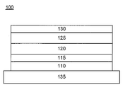
도 1은 기재 상에 형성된 반사 전극, 상기 반사 전극의 정상부 상의 유기 공여체-수용체 이종접합, 및 상기 공여체-수용체 이종접합의 정상부 상의 투명 전극을 포함하는 역전 유기 PV 디바이스를 나타낸다.
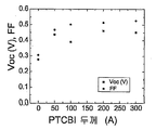
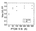
도 2a는 PTCBI 두께 대 에타(ηP - 전력 변환 효율) 및 반응도(JSC/P0)의 플롯이며, 여기서 A/W는 와트당 암페어를 나타내고, 'sim'은 '모의됨(simulated)'을 나타낸다.
도 2b는 PTCBI 대 V0C 및 FF의 플롯이다.
도 2c는 PTCBI 두께 대 직렬 저항(RS) 및 n의 플롯이다.
도 2d는 PTCBI 두께 대 역포화 전류(JS)의 플롯이다.
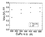
도 3a는 CuPc 두께 대 에타 및 JSC/PO의 플롯이다.
도 3b는 CuPc 대 V0C 및 FF의 플롯이다.
도 3c는 CuPc 두께 대 RS 및 n의 플롯이다.
도 3d는 CuPc 두께 대 JS의 플롯이다.
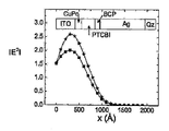
도 4a는 유리 상에 성장한 대조군 PV 디바이스: ITO (1550 Å)/CuPc (200 Å)/PTCBI (250 Å)/BCP (100 Å)/Ag (1000 Å) 상에서 실시된 표준 변환-매트릭스 시뮬레이션으로부터의 계산을 나타낸다. 625 nm에서의 CuPc(사각형) 및 540 nm에서의 PTCBI(별형)의 피크 흡수에서의 광학장이 도시되어 있다.
도 4b는 본 원에서 기술된 실시양태와 일치하는 역전 PV 디바이스: 석영/Ag (1000 Å)/BCP (100 Å)/PTCBI (300 Å)/CuPc (150 Å)/ITO (400 Å) 상에 실시된 표준 변환-매트릭스 시뮬레이션으로부터의 계산을 나타낸다. 625 nm에서의 CuPc(사각형) 및 540 nm에서의 PTCBI(별형)의 피크 흡수에서의 광학장이 도시되어 있다.
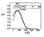
도 4c는 본 원에서 기술된 실시양태와 일치하는 역전 PV 디바이스: 석영/Ni (1000 Å)/CuPc (400 Å)/PTCBI (100 Å)/BCP (100 Å)/ITO (400 Å) 상에 실시된 표준 변환-매트릭스 시뮬레이션으로부터의 계산을 나타낸다. 625 nm에서의 CuPc(사각형) 및 540 nm에서의 PTCBI(별형)의 피크 흡수에서의 광학장이 도시되어 있다.
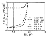
도 5a는 1 sun의 모의 조명 하(개방 원) 및 암실(충전된 사각형) 하의 유리 상에 성장한 대조군 PV 디바이스: ITO (1550 Å)/CuPc (200 Å)/PTCBI (250 Å)/BCP (100 Å)/Ag (1000 Å)에 대한 전류-전압 곡선을 나타낸다. 도 5a는 또한 1 sun의 모의 조명 하(개방 삼각형) 및 암실(충전 삼각형) 하의 본 원에서 기술된 실시양태와 일치하는 역전 PV 디바이스: 석영/Ni (1000 Å)/CuPc (400 Å)/PTCBI (100 Å)/BCP (100 Å)/ITO (400 Å)에 대한 전류-전압 곡선을 나타낸다. 상기 라인은 암실 전류 곡선에 맞는다.
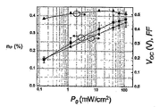
도 5b는 Ar 프라즈마 처리된 본 원에서 기술된 실시양태와 일치하는 역전 PV 디바이스: 석영/Ni (1000 Å)/CuPc (400 Å)/PTCBI (100 Å)/BCP (100 Å)/ITO (400 Å)에 대한 입사 전력 밀도의 함수로써의 ηP(사각형), VOC(별형) 및 FF(삼각형)을 나타낸다.
도 6a는 암실(사각형) 및 1 sun의 모의 AM1.5G 조명(점선) 하의 대조군 디바이스(유리/ITO (1550 Å)/CuPc (200 Å)/PTCBI (250 Å)/BCP (100 Å)/Ag (1000 Å)), 및 암실(삼각형) 및 조명(점선) 하의 본 원에서 기술된 실시양태와 일치하는 역전 PV 디바이스에 대한 전류-전압 특성치를 나타낸다.
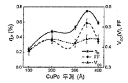
도 6b는 석영/Ni (1000 Å)/CuPc (350 Å)/PTCBI (100 Å)/BCP (100 Å)/ITO (400 Å)를 포함하는 역전 PV 디바이스에 대한 ηP(원형), VOC(삼각형) 및 FF(사각형)를 나타낸다.
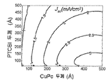
도 7a는 석영/Ni (1000 Å)/CuPc (x Å)/PTCBI (100 Å)/BCP (100 Å)/ITO (400 Å)를 포함하는 구조에서 CuPc 두께(x = 100∼400 Å)를 변화시키면서 역전 PV 디바이스의 1 sun 강도에서의 모의(선) 및 측정(충전된 사각형) 광전류를 나타낸다.
도 7b는 석영/Ni (1000 Å)/CuPc (x Å)/PTCBI (100 Å)/BCP (100 Å)/ITO (400 Å)를 포함하는 구조에서 CuPc 두께(x = 100∼400 Å)를 변화시키면서 역전 PV 디바이스의 1 sun의 AM1.5G 조명에서의 ηP(사각형), VOC(삼각형) 및 FF를 나타낸다.
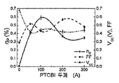
도 8a는 석영/Ni (1000 Å)/CuPc (400 Å)/PTCBI (y Å)/BCP (100 Å)/ITO (400 Å)를 포함하는 구조에서 PTCBI 두께(y = 0∼300 Å)를 변화시키면서 역전 PV 디바이스의 1 sun 강도에서의 모의(선) 및 측정(충전된 사각형) 광전류를 나타낸다.
도 8b는 석영/Ni (1000 Å)/CuPc (400 Å)/PTCBI (y Å)/BCP (100 Å)/ITO (400 Å)를 포함하는 구조에서 PTCBI 두께(y = 0∼300 Å)를 변화시키면서 역전 PV 디바이스의 1 sun의 AM1.5G 조명에서의 ηP(사각형), VOC(삼각형) 및 FF를 나타낸다.
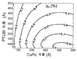
도 9a는 CuPc 및 PTCBI 두께의 함수로서의 JSC에 대한 모의 등고선 플롯을 나타낸다.
도 9b는 CuPc 및 PTCBI 두께의 함수로서의 ηP에 대한 모의 등고선 플롯을 나타낸다. 1 shows an inverted organic PV device comprising a reflective electrode formed on a substrate, an organic donor-receptor heterojunction on top of the reflecting electrode, and a transparent electrode on top of the donor-receptor heterojunction.
2A is a plot of PTCBI thickness versus eta (η P -power conversion efficiency) and reactivity (J SC / P 0 ), where A / W represents amperes per watt and 'sim' is 'simulated' Indicates.
2B is a plot of PTCBI vs V 0C and FF.
2C is a plot of PTCBI thickness versus series resistance (R S ) and n.
2D is a plot of PTCBI thickness versus antisaturation current (J S ).
3A is a plot of CuPc thickness versus eta and J SC / P O.
3B is a plot of CuPc vs V 0C and FF.
3C is a plot of CuPc thickness versus R S and n.
3D is a plot of CuPc thickness versus J S.
FIG. 4A shows control PV devices grown on glass: from standard transformation-matrix simulations run on ITO (1550 Hz) / CuPc (200 Hz) / PTCBI (250 Hz) / BCP (100 Hz) / Ag (1000 Hz) Indicates a calculation. The optical fields at peak absorption of CuPc (square) at 625 nm and PTCBI (star) at 540 nm are shown.
FIG. 4B shows inverted PV devices consistent with the embodiments described herein: quartz / Ag (1000 μs) / BCP (100 μs) / PTCBI (300 μs) / CuPc (150 μs) / ITO (400 μs) The calculations from the standard transform-matrix simulations performed are shown. The optical fields at peak absorption of CuPc (square) at 625 nm and PTCBI (star) at 540 nm are shown.
4C shows inverted PV devices consistent with the embodiments described herein: quartz / Ni (1000 μs) / CuPc (400 μs) / PTCBI (100 μs) / BCP (100 μs) / ITO (400 μs) The calculations from the standard transform-matrix simulations performed are shown. The optical fields at peak absorption of CuPc (square) at 625 nm and PTCBI (star) at 540 nm are shown.
FIG. 5A shows control PV devices grown on glass under simulated illumination (open circle) and dark room (filled squares) at 1 sun: ITO (1550 Hz) / CuPc (200 Hz) / PTCBI (250 Hz) / BCP (100 Iii) / Ag (1000 mA). FIG. 5A also shows a reverse PV device consistent with the embodiments described herein under simulated illumination (open triangle) and darkroom (charge triangle) of 1 sun: Quartz / Ni (1000 μs) / CuPc (400 μs) / PTCBI Current-voltage curves for (100 mA) / BCP (100 mA) / ITO (400 mA). The line fits the dark room current curve.
5B shows an inverted PV device consistent with the embodiments described herein with Ar plasma treatment: Quartz / Ni (1000 μs) / CuPc (400 μs) / PTCBI (100 μs) / BCP (100 μs) / ITO (400 Å) shows the η P (squares), V OC (star-shaped) and FF (triangles) as a function of incident power density on.
FIG. 6A shows control device under simulated AM1.5G illumination (dotted line) of darkroom (square) and 1 sun (Glass / ITO (1550 Hz) / CuPc (200 Hz) / PTCBI (250 Hz) / BCP (100 Hz) / Ag) (1000 Hz), and current-voltage characteristics for inverted PV devices consistent with the embodiments described herein under dark (triangle) and illumination (dashed lines).
FIG. 6B shows η P (circular), V OC for inverted PV devices including quartz / Ni (1000 μs) / CuPc (350 μs) / PTCBI (100 μs) / BCP (100 μs) / ITO (400 μs) (Triangle) and FF (square).
FIG. 7A shows the CuPc thickness (x = 100-400 Hz) in a structure including quartz / Ni (1000 Hz) / CuPc (x Hz) / PTCBI (100 Hz) / BCP (100 Hz) / ITO (400 Hz). Changes represent simulated (line) and measured (charged square) photocurrent at 1 sun intensity of inverted PV devices.
FIG. 7B shows the CuPc thickness (x = 100-400 μs) in a structure comprising quartz / Ni (1000 μs) / CuPc (x μs) / PTCBI (100 μs) / BCP (100 μs) / ITO (400 μs) Changes show η P (square), V OC (triangle), and FF in AM1.5G illumination of one sun of inverted PV devices.
8A shows the PTCBI thickness (y = 0 to 300 Hz) in a structure comprising quartz / Ni (1000 Hz) / CuPc (400 Hz) / PTCBI (y Hz) / BCP (100 Hz) / ITO (400 Hz). Changes represent simulated (line) and measured (charged square) photocurrent at 1 sun intensity of inverted PV devices.
8B shows the PTCBI thickness (y = 0 to 300 Hz) in a structure including quartz / Ni (1000 Hz) / CuPc (400 Hz) / PTCBI (y Hz) / BCP (100 Hz) / ITO (400 Hz). Changes show η P (square), V OC (triangle), and FF in AM1.5G illumination of one sun of inverted PV devices.
9A shows a simulated contour plot for J SC as a function of CuPc and PTCBI thickness.
9B shows a simulated contour plot for η P as a function of CuPc and PTCBI thickness.
역전 유기 감광성 광전자 디바이스가 본 원에서 기술된다. 기술되는 유기 디바이스는, 예를 들어 입사 전자기 방사선(예를 들어, PV 디바이스)로부터 사용가능한 전류를 발생시키는 데 사용할 수 있거나, 입사 전자기 방사선을 탐지하는 데 사용할 수 있다. 일부 실시양태는 애노드, 캐소드, 및 그 애노드와 캐소드 사이의 광활성 영역을 포함할 수 있다. 상기 광활성 영역은 전류를 발생시키기 위해 분리할 수 있는 여기자를 발생시키는 전자기 방사선을 흡수하는 감광성 디바이스의 일부이다. 기술되는 디바이스는 또한 1 이상의 투명 전극을 포함하여 입사 방사선이 상기 디바이스 내에 흡수되도록 할 수 있다. 몇몇 PV 디바이스 물질 및 배치가 미국 특허 6,657,378호, 6,580,027호 및 6,352,777호에 기술되어 있으며, 이는 PV 디바이스 물질 및 배치에 대한 이의 개시에 대해서 본 원에서 참조 인용된다.Inverted organic photosensitive optoelectronic devices are described herein. The organic device described can be used to generate a usable current from, for example, incident electromagnetic radiation (eg, a PV device), or can be used to detect incident electromagnetic radiation. Some embodiments may include an anode, a cathode, and a photoactive region between the anode and the cathode. The photoactive region is part of a photosensitive device that absorbs electromagnetic radiation that generates an excitable that can be separated to generate a current. The device described may also include one or more transparent electrodes to allow incident radiation to be absorbed within the device. Several PV device materials and arrangements are described in US Pat. Nos. 6,657,378, 6,580,027 and 6,352,777, which are incorporated herein by reference for their disclosure of PV device materials and arrangements.
본 원에서 사용되는 바와 같이, 용어 '층'은 주요 치수가 X-Y, 즉, 이의 길이 및 폭에 따른 것인 감광성 디바이스의 멤버 또는 성분을 의미한다. 상기 용어 층은 물질의 단일층 또는 시트 물질로 필히 한정되는 것이 아님이 이해되어야 한다. 또한, 상기 층과 다른 물질(들) 또는 층(들)과의 계면(들)을 포함하는 특정 표면은 불완전할 수 있으며, 여기서 상기 표면은 다른 물질(들) 또는 층(들)과 상호관통된, 얽힌 또는 감긴 네트워크를 나타낸다는 것이 이해되어야 한다. 유사하게는, 층은 그 층의 X-Y 치수에 따른 연속성이 다른 층(들) 또는 물질(들)로 방해 또는 그렇지 않으면 중단될 수 있어 비연속적일 수 있다는 것이 또한 이해되어야 한다. As used herein, the term 'layer' means a member or component of a photosensitive device whose main dimension is X-Y, ie its length and width. It is to be understood that the term layer is not necessarily limited to a single layer or sheet of material. In addition, certain surfaces, including interface (s) of the layer with other material (s) or layer (s), may be incomplete, where the surface may be interpenetrating with other material (s) or layer (s). It should be understood that this represents a tangled or wound network. Similarly, it should also be understood that a layer may be discontinuous as continuity along the X-Y dimension of the layer may be interrupted or otherwise interrupted by other layer (s) or material (s).
상기 용어 '전극' 및 '접점'은 광발생 전류을 외부 회로에 전달하거나, 바이어스 전류 또는 전압을 상기 디바이스에 제공하는 매체를 제공하는 층을 의미하는 데 사용된다. 즉, 전극 또는 접점은 유기 감광성 광전자 디바이스의 활성 영역과, 전선, 리드(lead), 트레이스(trace) 또는 전하 캐리어를 상기 외부 회로에 또는 이로부터 전달하는 기타 수단 사이의 계면을 제공한다. 예로는 애노드 및 캐소드가 있다. 전극의 개시에 대해서 본 원에서 참조 인용되는 미국 특허 6,352,777호는 감광성 광전자 디바이스에서 사용될 수 있는 전극 또는 접점의 예를 제공한다. 감광성 광전자 디바이스에서, 외부 디바이스로부터의 주위 전자기 방사선의 최대량이 상기 광전도성 활성 내부 영역으로 진입하도록 허용하는 것이 바람직하다. 즉, 상기 전자기 방사선은 광전도층(들)에 도달해야 하며, 여기서 이는 광전도성 흡수에 의해 전기로 전환될 수 있다. 이는 흔히 상기 전기 접점이 상기 입사 전자기 방사선을 최소한으로 흡수하고 최소한으로 반사시켜야 한다는 것을 나타낸다. 일부 경우에서, 상기 접점은 실질적으로 투명해야 한다. 상기 반대 전극은 반사성 물질이어서 상기 전극을 통과한 광을 흡수됨 없이 상기 전지를 통해 반사시킬 수 있다. 본 원에서 사용되는 바와 같이, 물질의 층 또는 일련의 상이한 물질의 몇몇 층들은, 상기 층 또는 층들이 관련 파장에서의 주위 전자기 방사선 중 약 50% 이상을 그 층 또는 층들을 통해 전도되도록 허용하는 경우에 '투명하다'고 일컬어진다. 유사하게는, 관련 파장에서 주위 전자기 방사선의 일부, 그러나 약 50% 미만을 전달할 수 있는 층은 '반투명하다'라고 일컬어진다.The terms 'electrode' and 'contact' are used to mean a layer that delivers a photo-generated current to an external circuit or provides a medium for providing a bias current or voltage to the device. That is, the electrode or contact provides an interface between the active region of the organic photosensitive optoelectronic device and other means for transferring wires, leads, traces or charge carriers to or from the external circuit. Examples are anodes and cathodes. US Pat. No. 6,352,777, which is incorporated herein by reference for the disclosure of the electrodes, provides examples of electrodes or contacts that can be used in photosensitive optoelectronic devices. In photosensitive optoelectronic devices, it is desirable to allow the maximum amount of ambient electromagnetic radiation from an external device to enter the photoconductive active inner region. That is, the electromagnetic radiation must reach the photoconductive layer (s), where it can be converted to electricity by photoconductive absorption. This often indicates that the electrical contact should absorb minimally and reflect the incident electromagnetic radiation. In some cases, the contact should be substantially transparent. The counter electrode is a reflective material and can reflect through the cell without absorbing light passing through the electrode. As used herein, a layer of material or some layers of a series of different materials allow the layer or layers to conduct at least about 50% of ambient electromagnetic radiation at the relevant wavelengths through the layer or layers. Is said to be transparent. Similarly, a layer capable of delivering a portion of the ambient electromagnetic radiation, but less than about 50%, at a relevant wavelength is said to be 'translucent'.
상기 용어 '캐소드'는 하기 방식으로 이용된다. 주위 방사선 하에 저항 부하와 연결되고 내부 인가 전압이 없는 비적층형 PV 디바이스, 또는 적층형 PV 디바이스의 단일 유닛에서, 전자는 상기 광전도성 물질로부터 상기 캐소드로 이동한다. 유사하게는, 본 원에서 상기 용어 '애노드'는, 조명 하의 PV 디바이스에서 정공이 광전도성 물질로부터 애노드로 이동하고, 이는 반대 방식으로 이동하는 전자와 동등한 것처럼 사용된다. 상기 용어가 본 원에서 사용되는 바와 같이 애노드 및 캐소드는 전극 또는 전하 수송층일 수 있다는 것이 주지되게 된다. 본 원에서 사용되는 바와 같이, '정상부'는 상기 기재 구조(존재하는 경우)로부터 가장 멀다는 것을 의미하는 반면에, '바닥부'는 상기 기재 구조에 가장 가깝다는 것을 의미한다. 상기 디바이스가 기재 구조체를 포함하지 않는 경우, '정상부'는 상기 반사 전극으로부터 가장 멀다는것을 의미한다. 예를 들어, 2개의 전극을 갖는 디바이스에 대해서, 상기 바닥부 전극은 상기 기재 구조에 가장 가까운 전극이며, 일반적으로 제조된 제1 전극이다. 상기 바닥부 전극은 상기 기재에 가장 가까운 바닥부 측면 및 상기 기재로부터 가장 먼 정상부 측면의 2개의 표면을 가진다. 제1 층이 제2 층 '상에 배치된' 또는 '의 정상부 상에 있는'이라 기술되는 경우에, 상기 제1 층은 기재로부터 멀리 떨어져 배치되어 있다. 상기 제1 층이 상기 제2 층'과 물리적으로 접촉'한다는 것이 명시되지 않는 경우, 상기 제1 및 제2 층 사이에 다른 층들이 존재할 수 있다. 예를 들어, 캐소드는 애노드 '상에 배치된다' 또는 '의 정상부 상에 있다'는 것으로 기술될 수 있으나, 이들 사이에 다양한 유기층들이 존재한다.The term 'cathode' is used in the following manner. In a single unit of a non-laminated PV device, or stacked PV device, connected to a resistive load under ambient radiation and without an internally applied voltage, electrons move from the photoconductive material to the cathode. Similarly, the term 'anode' is used herein as if holes in a PV device under illumination move holes from the photoconductive material to the anode, which is equivalent to electrons traveling in the opposite way. It is to be noted that as the term is used herein, the anode and cathode can be an electrode or a charge transport layer. As used herein, 'top' means the furthest from the substrate structure (if present), while 'bottom' means the closest to the substrate structure. If the device does not include a substrate structure, the 'normal' means the furthest from the reflective electrode. For example, for a device having two electrodes, the bottom electrode is the electrode closest to the base structure, and is generally the first electrode manufactured. The bottom electrode has two surfaces, a bottom side closest to the substrate and a top side farthest from the substrate. When the first layer is described as 'disposed on' or 'on top of' the second layer, the first layer is disposed away from the substrate. If it is not specified that the first layer is in physical contact with the second layer, there may be other layers between the first and second layers. For example, the cathode may be described as 'positioned on' or 'on top of the anode', but there are various organic layers between them.
도 1은 역전 유기 감광성 광전자 디바이스(100)를 나타낸다. 상기 도는 일정 비율로 도시될 필요는 없다. 디바이스(100)는 반사 기재(110), 공여체층(115), 수용체층(120), 임의의 차단층(125) 및 투명 전극(130)을 포함할 수 있다. 디바이스(100)는 순차적으로 상기 기술된 층들을 침착시켜 제조할 수 있다. 일부 실시양태에서, 도 1에서 기술되는 디바이스는 투명성에 영향을 받지 않도록 차단층(125) 및 투명 전극(130) 사이에 매우 얇은 손상 유도 금속층을 임의로 포함할 수 있다. 디바이스(100)는 또한 기재 구조체(135)를 임의로 포함할 수 있다. 일부 실시양태에서, 상기 기재 구조체는 반사 전극(110)을 직접 지지할 수 있다.1 shows an inverted organic photosensitive
도 1에서 예시되는 층들의 특정 배열은 단지 예시적인 것이며, 한정하려는 의도는 아니다. 예를 들어, 상기 층들 중 일부(예컨대 차단층)는 생략될 수 있다. 다른 층들(예컨대 반사 전극 또는 추가 수용체 및 공여체 층)이 첨가될 수 있다. 층들의 순서는 변경될 수 있다. 특정 기술된 것들 이외의 배열이 적용될 수 있다. 또한, 상기 유기 PV 디바이스는 1 이상의 추가 공여체-수용체 층을 포함하는 탠덤 디바이스로서 존재할 수 있다. 탠덤 디바이스는 탠덤 공여체-수용체 층 사이에 전하 이송층, 전극 또는 전하 재조합층을 포함할 수 있다. 상기 기재 및 반사 전극은 조합될 수 있으며, 상기 기재는 반사성일 수 있고, 상기 전극은 투명할 수 있다. The particular arrangement of layers illustrated in FIG. 1 is merely illustrative and is not intended to be limiting. For example, some of the layers (eg, blocking layers) may be omitted. Other layers may be added, such as reflective electrodes or additional acceptor and donor layers. The order of the layers can be changed. Arrangements other than those specifically described may be applied. The organic PV device may also exist as a tandem device comprising one or more additional donor-receptor layers. Tandem devices may include a charge transfer layer, an electrode, or a charge recombination layer between tandem donor-receptor layers. The substrate and the reflective electrode can be combined, the substrate can be reflective, and the electrode can be transparent.
디바이스가 성장하거나 위치할 수 있는 기재(135)는 소정의 구조적 특성을 제공하는 임의의 적합한 물질일 수 있다. 상기 기재는 경성 또는 연성, 평면 또는 비평면일 수 있다. 상기 기재는 투명, 반투명 또는 불투명할 수 있다. 플라스틱, 유리 및 석영은 경성 기재 물질의 예이다. 플라스틱 및 금속 호일은 연성 기재 물질의 예이다. 상기 기재의 재료 및 두께는 소정의 구조 및 광학 특성을 얻도록 선택될 수 있다. The
일부 실시양태에서, 상기 반사 전극(110)은 전극, 예컨대 금속 애노드를 포함할 수 있다. 일부 실시양태에서, 반사 전극(110)은 스틸, Ni, Ag, Al, Mg, In, 및 이들의 혼합물 또는 합금으로부터 선택되는 낮은 일함수의 금속을 포함할 수 있다. 일부 실시양태에서, 상기 전극은 베이스로서 하나의 금속, 및 전극 물질로서 Ti, 스테인레스 스틸, 또는 Ag이 위에 존재 또는 부재하는 Al 시트와 같은 것을 포함할 수 있다.In some embodiments, the
일부 실시양태에서, 반사 전극(110) 및 기재 물질(135)은 2개의 금속으로 조합 또는 형성될 수 있다. 일부 실시양태에서, 기재(135)는 반응성이고, 전극(110)은 투명하다.In some embodiments,
일부 실시양태에서, 본 원에서 기술되는 '전극'은 '금속' 또는 '금속 대체물'로 구성될 수 있다. 본 원에서, 상기 용어 '금속'은 원소 순수 금속, 예를 들어 Mg로 구성된 물질, 및 또한 2 이상의 원소 순수 금속, 예를 들어 Mg 및 Ag로 함께 구성된 Mg:Ag를 의미하는 물질인 금속 합금 둘 모두를 포괄하는 데 사용된다. 여기서, 상기 용어 '금속 대체물'은 일반적인 정의 내의 금속이 아니나 적절한 특정 용도에서 바람직한 금속유사 특성을 보유하는 물질을 의미한다. 전극 및 전하 수송층에 일반적으로 사용되는 금속 대체물은 넓은 밴드갭의 도핑된 반도체, 예를 들어 투명한 전도성 산화물, 예컨대 인듐 주석 산화물(ITO), 갈륨 인듐 주석 산화물(GITO) 및 아연 인듐 주석 산화물(ZITO)을 포함할 수 있다. 특히, ITO는 대략 3900 Å 초과의 파장에 대해서 이를 투명하게 하는 대략 3.2 eV의 광학 밴드갭을 갖는 고도로 도핑된 축퇴형 n+ 반도체이다. 또다른 적합함 금속 대체물로는 투명한 전도성 중합체인 폴리아날린(PANI) 및 이의 화학적 관련물이 있다.In some embodiments, an 'electrode' described herein can be composed of a 'metal' or a 'metal substitute'. As used herein, the term 'metal' refers to a metal alloy that is a material meaning an elemental pure metal, eg, Mg, and also a Mg: Ag, composed of two or more elemental pure metals, eg, Mg and Ag. Used to cover everything. Here, the term 'metal substitute' means a material which is not a metal in the general definition but retains the metal-like properties desirable for the particular application. Metal substitutes commonly used in electrodes and charge transport layers are wide bandgap doped semiconductors, for example transparent conductive oxides such as indium tin oxide (ITO), gallium indium tin oxide (GITO) and zinc indium tin oxide (ZITO). It may include. In particular, ITO is a highly doped degenerate n + semiconductor with an optical bandgap of approximately 3.2 eV that makes it transparent for wavelengths greater than approximately 3900 GHz. Another suitable metal substitute is polyaniline (PANI), which is a transparent conductive polymer, and its chemical associations.
금속 대체물은 광범위한 비금속성 물질로부터 추가로 선택될 수 있으며, 여기서 상기 용어 '비금속성'은 광범위한 물질을 포괄하는 것을 의미하고, 단, 상기 물질은 화학적으로 비결합된 형태의 금속을 포함하지 않는다. 금속이 이의 화학적으로 비결합된 형태로 존재하는 경우, 단독으로 또는 1 이상의 다른 금속과 합금으로서 상기 금속은 이의 금속성 형태로 존재하는 것으로 또는 '비금속'인 것으로 대안적으로 언급될 수 있다. 따라서, 본 원에서 기술된 금속 대체물 전극은 '비금속'이라 때때로 언급될 수 있으며, 여기서 상기 용어 '무금속'이 화학적으로 비결합된 형태의 금속을 포함하지 않는 물질을 포괄하는 것으로 명확히 의미된다. 비금속은 전형적으로 금속 격자 전반에 걸쳐 전자 전도대에서 이동하는 데 자유로운 원자가 전자의 바다로부터 유래하는 금속성 결합의 형태를 전형적으로 보유한다. 금속 대체물은 금속 구성 성분을 함유할 수 있지만, 이들은 몇몇 베이스 상에서 '비금속성'이다. 이들은 순수한 비금속이 아니며, 또한 비금속들의 합금도 아니다. 금속이 이의 금속 형태로 존재하는 경우에, 상기 전자 전도대는 다른 금속 특성들 중에서도 광학 방사선에 대한 높은 반사도뿐만 아니라 높은 전기 전도도를 제공하는 경향이 있다.The metal substitute may be further selected from a wide range of nonmetallic materials, wherein the term 'nonmetallic' means to cover a wide range of materials, provided that the material does not include a metal in a chemically unbound form. Where a metal is present in its chemically unbound form, it may be alternatively referred to as being alone or as an alloy with one or more other metals as being in its metallic form or being 'nonmetal'. Accordingly, the metal substitute electrode described herein may sometimes be referred to as a 'non-metal', where the term 'metal-free' is clearly meant to encompass materials that do not contain a chemically unbonded form of metal. Nonmetals typically possess a form of metallic bond derived from the sea of valence electrons that is free to move in the electron conduction band across the metal lattice. Metal substitutes may contain metal components, but they are 'nonmetallic' on some bases. They are not pure nonmetals, nor are they alloys of nonmetals. Where metal is in its metal form, the electron conduction band tends to provide high electrical conductivity as well as high reflectivity to optical radiation, among other metal properties.
투명 전극(130)은 투명 산화물, 및 투명하게 되기에 충분한 두께를 갖는 금속 또는 금속 대체물로부터 선택될 수 있다. 전극 및 전하 이송층에 대해서 일반적으로 사용되는 금속 대체물은 넓은 밴드갭의 도핑된 반도체, 예컨대 투명한 전도성 산화물을 포함할 수 있다. 일부 실시양태에서, 투명 전극(130)은 ITO, GITO 및 ZITO로부터 선택될 수 있다. 다른 예시적 전극으로는 Parthasarathy 등의 미국 특허 6,420,031호에 개시된 바와 같은 매우 투명한 비금속성의 저저항 캐소드, 또는 Forrest 등의 미국 특허 5,703,436호에 개시된 고효율의 저저항 금속성/비금속성 화합물 캐소드를 들 수 있으며, 상기 특허 둘 모두는 이의 캐소드 개시에 대해서 본 원에서 참조 인용되어 있다. 각각의 유형의 캐소드는 ITO 층을 유기 물질, 예컨대 CuPc에 스퍼터 침착시켜 고도로 투명한 비금속성의 저저항 캐소드를 형성하거나, 얇은 Mg:Ag 층에 스퍼터 침착시켜 고효율의 저저항 금속성/비금속성 화합물 캐소드를 형성하는 단계를 포함하는 제조 공정에서 전형적으로 제조된다.
본 원에서 기술되는 디바이스는 광이 흡수되어 후에 전자 또는 정공으로 분리될 수 있는 여기 상태 또는 '여기자'를 형성하는 1 이상의 광활성 영역을 포함하게 된다. 상기 여기자의 분리는 전형적으로 공여체층 및 수용체층의 병치에 의해 형성되는 '이종접합'에서 전형적으로 발생하게 된다. 예를 들어, 도 1의 디바이스에서, '광활성 영역'은 공여체층(115) 및 수용체층(120)을 포함할 수 있다. 전하 분리가 공여체층(115)과 수용체층(120) 사이의 유기 이종접합에서 주로 발생할 수 있다. 상기 이종접합에서의 내부 전위는 접촉하여 상기 이종접합을 형성하는 2개의 물질 사이의 HOMO-LUMO 에너지 수준차에 의해 측정한다. 상기 공여체와 수용체 물질 사이의 HOMO-LUMO 갭 오프셋은 공여체-수용체 계면의 여기자 확산 길이 내에서 생성되는 여기자의 반대 부호 캐리어(정공 및 전자)로의 분리를 촉진하는 상기 계면에서의 전기장을 형성한다.The devices described herein will include one or more photoactive regions that form an excited state or 'exciton' where light can be absorbed and subsequently separated into electrons or holes. Separation of the exciton typically occurs at 'heterojunctions' formed by juxtaposition of the donor and acceptor layers. For example, in the device of FIG. 1, the 'photoactive region' may comprise a
수용체층(120)을 포함하는 적합한 물질로는, 예를 들어 중합 또는 비중합 페릴렌, 나프탈렌, 풀러렌 또는 나노튜블을 들 수 있다. 일부 실시양태에서, 수용체층(120)은 3,4,9,10-페릴렌테트라카르복실산 비스-벤즈이미다졸(PTCBI)을 들 수 있다. 다른 실시양태에서, 수용체층(120)은 미국 특허 6,580,027호에 기술되어 있는 바와 같은 풀러렌 물질을 포함할 수 있으며, 상기 특허의 풀러렌 설명은 그 전체로 본 원에서 참조 인용되어 있다. 일부 실시양태에서, 공여체층(115)은 스쿠아레인, 프탈로시아닌, 포르피린, 서브프탈로시아닌(SubPc), 구리 프탈로시아닌(CuPc), 또는 이의 유도체 또는 전이 금속 착물, 예컨대 알루미늄 프탈로시아닌 클로라이드(AlClPc)를 포함할 수 있다. Suitable materials including the
상기 광활성층에 사용하는 데 적합한 다른 물질로는 고리금속화 유기금속성 화합물을 들 수 있다. 본 원에서 사용되는 용어 '유기금속성'은, 예를 들어 문헌["Inorganic Chemistry" (2nd Edition) by Gary L. Miessler and Donald A. Tarr, Prentice Hall (1998)]에서 제시되고, 당업자에게 일반적으로 이해되는 바와 같다. 따라서, 상기 용어 유기금속성은 탄소-금속 결합을 통해 금속에 결합된 유기기를 갖는 화합물을 의미할 수 있다. 유기금속 화합물은 유기 화학종으로의 1 이상의 탄소-금속 결합 이외에 이종원자로부터의 1 이상의 공여체 결합을 포함할 수 있다. 유기 화학종으로의 탄소-금속 결합은, 예를 들어 금속과, 유기기, 예컨대 페닐, 알킬, 알케닐 등의 탄소 원자 사이의 직접 결합을 의미할 수 있다. 상기 용어 고리금속화는 2자리 유기금속 리간드를 포함하여 금속으로의 결합 시 고리 구성원 중 하나로서 금속을 포함하는 고리 구조를 형성하는 화합물을 의미한다. Other materials suitable for use in the photoactive layer include ring metallized organometallic compounds. The term 'organometallic' as used herein is given, for example, in "Inorganic Chemistry" (2nd Edition) by Gary L. Miessler and Donald A. Tarr, Prentice Hall (1998), and generally to those skilled in the art. As understood. Thus, the term organometallic may mean a compound having an organic group bonded to the metal through a carbon-metal bond. The organometallic compound may comprise one or more donor bonds from heteroatoms in addition to one or more carbon-metal bonds to the organic species. Carbon-metal bonds to organic species may mean, for example, direct bonds between metals and carbon atoms of organic groups such as phenyl, alkyl, alkenyl and the like. The term ring metallization means a compound comprising a bidentate organometallic ligand that forms a ring structure comprising a metal as one of the ring members upon binding to the metal.
용어 '층'에 관련하여 상기 언급된 바와 같이, 도 1에 도시된 바와 같은 수용체층(120)과 공여체층(115)의 경계는 불완전, 비연속 및/또는 그렇지 않으면 공여체 및 수용체 물질 상호관통된, 얽힌 또는 감긴 네트워크를 나타내는 것으로 이해되어야 한다. 예를 들어, 일부 실시양태에서, 상기 유기 공여체-수용체 이종접합은 평면 이종접합을 형성할 수 있으나, 한편으로는, 벌크 이종접합, 나노결정질 벌크 이종접합, 혼성 평면-혼합 이종접합 또는 혼합 이종접합을 형성할 수 있다. 일부 실시양태에서, 2 이상의 유기 공여체-수용체 이종접합을 사용하여 탠덤 역전 PV 디바이스를 생성할 수 있다.As noted above with respect to the term 'layer', the boundary between the
유기 층은 진공 침착, 스핀 코팅, 유기 증착, 잉크젯 인쇄 또는 당업계에 공지된 다른 방법을 이용하여 제작할 수 있다. The organic layer can be fabricated using vacuum deposition, spin coating, organic deposition, ink jet printing or other methods known in the art.
본 원에서 기술되는 실시양태의 유기 감광성 광전자 디바이스는 PV 디바이스, 광검출기 또는 광전도체로서 작용할 수 있다. 본 원에서 기술되는 유기 감광성 광전자 디바이스가 PV 디바이스로서 작용할 때마다, 상기 광전도성 유기층에서 사용되는 물질 및 이의 두께는, 예를 들어 상기 디바이스의 외부 양자 효율을 최적화시키도록 선택될 수 있다. 본 원에서 기술되는 유기 감광성 광전자 디바이스가 광검출기 또는 광전도체로서 작용할 때마다, 상기 광전도성 유기층에서 사용되는 물질 및 이의 두께는, 예를 들어 소정의 스펙트럼 영역으로의 상기 디바이스의 선택도를 최대화시키도록 선택될 수 있다.The organic photosensitive optoelectronic devices of the embodiments described herein can act as PV devices, photodetectors or photoconductors. Each time the organic photosensitive optoelectronic device described herein acts as a PV device, the material used in the photoconductive organic layer and its thickness can be selected, for example, to optimize the external quantum efficiency of the device. Whenever the organic photosensitive optoelectronic device described herein acts as a photodetector or photoconductor, the material used in the photoconductive organic layer and its thickness may, for example, maximize the selectivity of the device to a predetermined spectral region. May be selected.
소정의 결과는 층 두께 선택에 적용될 수 있는 몇몇 지침을 고려하여 달성할 수 있다. 상기 층 두께 L은 여기자 확산 길이 LP보다 작거나 그 정도 되는 것이 바람직할 수 있으며, 이는 대부분의 여기자 분리가 공여체-수용체 계면의 확산 길이 내에서 발생하게 되는 것으로 생각되기 때문이다. 상기 설명에서, L은 상기 여기자 형성 부분 및 공여체-수용체 계면으로부터의 거리이다. L이 LD보다 큰 경우, 많은 여기자가 분리 전에 재결합할 수 있다. 상기 광전도성 층의 전체 두께는 전자기 방사선 흡수 길이 1/α(여기서, α는 흡수 계수임) 정도이게 되어 PV 디바이스 상에 입사하는 거의 모든 방사선이 흡수되어 여기자가 생성되는 것이 더욱 바람직하다. 더욱이, 상기 광전도성 층의 두께는 유기 반도체의 높은 벌크 저항으로 인한 과도한 직렬 저항을 피하도록 가능한 얇아야 한다.Certain results can be achieved by considering some guidelines that can be applied to the choice of layer thickness. It may be desirable for the layer thickness L to be less than or equal to the exciton diffusion length L P , since most exciton separation is believed to occur within the diffusion length of the donor-receptor interface. In the above description, L is the distance from the exciton-forming part and the donor-receptor interface. If L is greater than L D , many excitons can recombine before separation. More preferably, the total thickness of the photoconductive layer is on the order of electromagnetic
따라서, 이러한 경쟁적 지침은 감광성 광전자 전지의 광전도성 유기층의 두께를 선택하는 데 형성되는 트레이드오프를 본래 필요로 할 수 있다. 따라서, 한편, 상기 흡수 길이와 대등하거나 이보다 큰 두께가 최대량의 입사 방사선을 흡수하기 위해 바람직할 수 있다. 한편, 광전도성 층 두께가 증가함에 따라, 2개의 바람직하지 않은 효과가 증가할 수 있다. 하나는 유기 반도체의 높은 직렬 저항으로 인해 유기층 두께가 증가하여 디바이스 저항이 증가하고 효율이 감소할 수 있다는 것이다. 또다른 바람직하지 않은 효과는 상기 광전도성 층의 두께를 증가시키는 것이, 전하 분리 계면으로부터 멀리 여기자가 발생되어 제짝 재결합의 확률을 증가시키고 재차 효율을 감소시키게 될 가능성을 증가시킬 수 있다는 것이다. 따라서, 전체 디바이스에 대해서 높은 외부 양자 효율을 생성하는 방식으로 상기 경쟁 효과들의 균형을 맞추는 디바이스 배열을 갖는 것이 바람직할 수 있다. Thus, this competitive guidance may inherently require a tradeoff that is formed to select the thickness of the photoconductive organic layer of the photosensitive optoelectronic cell. Thus, on the other hand, a thickness comparable to or greater than the absorption length may be desirable to absorb the maximum amount of incident radiation. On the other hand, as the photoconductive layer thickness increases, two undesirable effects may increase. One is that due to the high series resistance of organic semiconductors, the organic layer thickness can increase, resulting in increased device resistance and reduced efficiency. Another undesirable effect is that increasing the thickness of the photoconductive layer can increase the likelihood that excitons are generated away from the charge separation interface, increasing the probability of even recombination and again decreasing the efficiency. Thus, it may be desirable to have a device arrangement that balances the competitive effects in a manner that produces high external quantum efficiency for the entire device.
도 1의 디바이스는 미국 특허 6,097,147호(Peumans 등), 문헌[Applied Physics Letters 2000, 76, 2650-52] 및 미국 특허 6,451,415호(Forrest 등)에 기술된 1 이상의 차단층(125), 예컨대 여기자 차단층(EBL)을 추가로 포함할 수 있으며, 상기 문헌은 이의 차단층 개시에 대해서 본 원에 참조 인용되어 있다. 특정 실시양태에서, 높은 내부 및 외부 양자 효율은, 광발생된 여기자를 상기 분리 계면 근처의 영역으로 한정하고 기생 여기자가 감광성 유기/전자 계면에서 켄칭하는 것을 방지하는 EBL을 포함하여 달성하였다. 여기자가 확산할 수 있는 부피를 한정하는 것 이외에, EBL은 또한 상기 전극의 침착 중에 유입되는 물질에 대한 확산 배리어로서 작용할 수 있다. 일부 환경에서, EBL은 비작용성의 유기 PV 디바이스가 될 수 있는 핀홀 또는 단락성 결함을 채우기에 충분히 두껍게 제조할 수 있다. 따라서, EBL은 취약한 유기 층을, 그 유기 물질 상에 전극이 침착되는 경우에 생성되는 손상으로부터 보호하는 데 일조할 수 있다. The device of FIG. 1 includes one or more blocking layers 125, such as exciton blocking, described in US Pat. No. 6,097,147 (Peumans et al.),
어떠한 특정 이론에도 얽매임 없이, EBL은 여기자가 차단되는 인접 유기 반도체보다 실질적으로 큰 LUMO-HOMO 에너지 갭을 갖는 것으로부터 이의 여기자 차단 특성을 유도하는 것으로 생각된다. 따라서, 상기 한정된 여기자는 에너지를 고려하면 EBL에 존재하는 것이 금지된다. EBL이 여기자를 차단하는 것이 바람직하지만, 그 EBL이 모든 전하를 차단하는 것은 바람직하지 않다. 그러나, 인접 에너지 수준의 특성으로 인해, EBL은 전하 캐리어의 한 신호를 차단할 수 있다. 설계에 의해, EBL은 2개의 다른 층, 일반적으로 유기 감광성 반도체 층과 전극, 전하 수송층 또는 전하 재결합층 사이에 존재하게 된다. 인접하는 전극 또는 전하 수송층은 내용 상 캐소드 또는 애노드이게 된다. 따라서, 디바이스 중 소정 위치에서의 EBL에 대한 물질은 캐리어의 소정 신호가 그 전달 중에 전극 또는 전하 수송층으로 지연되지 않도록 선택되게 된다. 에너지 수준을 적절히 정렬함으로써, 전하 수송에 대한 배리어가 존재하지 않아 직렬 저항이 증가하는 것을 방지할 수 있다. 특정 실시양태에서, 캐소드 측 EBL로서 사용되는 물질은 상기 인접하는 수용체 물질의 LUMO 에너지 수준과 밀접하게 매칭하는 LUMO 에너지 수준을 가짐으로써 전자에 대한 바람직하지 않은 임의의 배리어를 최소화시키는 것이 바람직할 수 있다.Without being bound by any particular theory, it is believed that EBL derives its exciton blocking properties from having a substantially larger LUMO-HOMO energy gap than adjacent organic semiconductors in which excitons are blocked. Therefore, the limited excitons are prohibited from being present in the EBL in consideration of energy. While it is desirable for the EBL to block excitons, it is undesirable for the EBL to block all charges. However, due to the nature of the adjacent energy levels, the EBL can block one signal of the charge carriers. By design, the EBL is present between two different layers, generally an organic photosensitive semiconductor layer and an electrode, a charge transport layer or a charge recombination layer. Adjacent electrodes or charge transport layers become cathodes or anodes in their contents. Thus, the material for the EBL at certain locations in the device is selected such that certain signals of the carrier are not delayed to the electrode or charge transport layer during its transfer. By properly aligning the energy levels, there is no barrier to charge transport, thereby preventing the series resistance from increasing. In certain embodiments, it may be desirable for the material used as cathode side EBL to have an LUMO energy level that closely matches the LUMO energy level of the adjacent receptor material, thereby minimizing any undesirable barriers to electrons. .
물질의 여기자 차단 특성은 실질적으로 이의 HOMO-LUMO 에너지 갭의 고유 특성이 아님이 이해되어야 한다. 소정의 물질이 여기자 차단체로서 작용하는지에 대한 여부는 상기 인접하는 유기 감광성 물질의 상대적인 HOMO 및 LUMO 에너지 수준에 따라 다르다. 따라서, 사용될 수 있는 디바이스 구조를 고려하지 않고 여기자 차단체로서 별개로 화합물의 부류를 확인하는 것은 불가능할 수 있다. 그러나, 본 원에서의 교시에 의해, 당업자는 소정의 물질이 선택된 물질 세트와 함께 유기 PV 디바이스를 구성하는 데 사용되는 경우에 여기자 차단층으로서 작용하게 되는지에 대한 여부를 확인할 수 있다.It should be understood that the exciton blocking property of a material is not substantially the inherent property of its HOMO-LUMO energy gap. Whether a given material acts as an exciton blocker depends on the relative HOMO and LUMO energy levels of the adjacent organic photosensitive material. Thus, it may be impossible to identify the class of compounds separately as exciton blockers without considering the device structures that can be used. However, the teachings herein allow one skilled in the art to ascertain whether a given material will act as an exciton blocking layer when used in constructing an organic PV device with a selected set of materials.
일부 실시양태에서, 차단층(125)은 수용체층(120)과 투명 전극(130) 사이에 위치한 EBL을 포함할 수 있다. 적합한 EBL 물질의 예로는 비한정적으로 2,9-디메틸-4,7-디페닐-1,10-페난트롤린(또한, 바쏘쿠프로인 또는 BCP이라 일컬음)(이는 LUMO-HOMO 에너지 수준 분리가 약 3.5 eV인 것으로 생각됨), 또는 비스(2-메틸-8-히드록시퀴놀리노아토)-알루미늄(Ⅲ)페놀레이트(Alq2OPH)를 포함한다. BCP는 전자를 수용체층으로부터 상기 캐소드로 용이하게 수송할 수 있는 효과적인 여기자 차단체일 수 있다. 다른 실시양태에서, 상기 EBL은 N,N'-디페닐-N,N'-비스-알파-나프틸벤지딘(NPD), 알루미늄 트리스(8-히드록시퀴놀린)(Alq3), 카르바졸 비페닐(CBP) 및 트리스(아세틸아세토네이토) 루테늄(Ⅲ)(Ru(acac)3)으로부터 선택될 수 있다.In some embodiments, blocking
일부 실시양태에서, 차단층(125)은 적합한 도판트, 예컨대 비한정적으로 3,4,9,10-페릴렌테트라카르복실산 이무수물(PTCDA), 3,4,9,10-페릴렌테트라카르복실산 디이미드(PTCDI), 3,4,9,10-페릴렌테트라카르복실산-비스-벤즈이미다졸(PTCBI), 1,4,5,8-나프탈렌테트라카르복실산 이무수물(NTCDA) 및 이의 유도체에 의해 도핑되는 EBL을 포함할 수 있다. 본 발명에서 기술되는 디바이스에서 침착되는 바와 같이 BCP는 비결정질일 수 있다. 비결정질인 BCP 여기자 차단층은 필름 재결정화를 나타낼 수 있으며, 이는 높은 광도 하에서 특히 신속할 수 있다. 생성되는 다결정질 물질로의 형태 변화는 전극 물질의 단락, 공극 또는 간섭과 같은 가능한 결함을 갖는 저품질 필름을 유발시킨다. 따라서, 이러한 효과를 나타내는 일부 EBL 물질, 예컨대 BCP를 적합하고 상대적으로 크며 안정한 분자에 의해 도핑하는 것은 상기 EBL 구조를 안정화시켜 성능이 감퇴하는 형태 변화를 방지할 수 있다는 것이 확인되었다. 소정의 디바이스 중 전자를 수송하는 EBL을 그 EBL에 근접하는 LUMO 에너지 수준을 갖는 물질에 의해 도핑하는 것은 공간 전하 증가를 생성하고 성능을 감소시킬 수 있는 전자 포획을 형성하지 않도록 하는 데 일조할 수 있다는 것이 추가로 이해되어야 한다. 또한, 상대적으로 낮은 도핑 밀도는 분리된 도판트 부위에서의 여기자 생성을 최소화시켜야 한다는 것이 이해되어야 한다. 이러한 여기자는 주위 EBL 물질에 의한 확산으로부터 효과적으로 방지되기 때문에, 이러한 흡수는 디바이스 광변환 효율을 감소시킨다.In some embodiments, the
일부 실시양태에서, 도 1의 디바이스는 1 이상의 투명 전하 수송층 또는 전하 재결합층을 추가로 포함할 수 있다. 본 원에서 기술되는 바와 같이, 전하 수송층은 전하 수송층이 흔히 그러나 필수적이지는 않게 무기(흔히 금속)이고 광전도성으로 활성이지 않게 선택될 수 있다는 사실로부터 수용체 및 공여체 층과는 구별된다. 용어 '전하 수송층'은 본 원에서 사용되어, 전하 수송층이 전하 캐리어를 광전자 디바이스의 일부로부터 인접하는 일부로 단지 전달하는 전극과 유사하나 상이한 층을 의미한다. 용어 '전하 재결합층'은 본 원에서 사용되어, 전하 재결합층이 탠덤 감광성 디바이스들 사이의 전자 및 정공의 재결합을 허용하고 또한 1 이상의 활성층 근처의 내부 광학장 강도를 증대시킬 수 있는 전극과 유사하나 상이한 층을 의미한다. 전하 재결합층은 본 원에서 참조 인용되어 있는 미국 특허 6,657,378호에 기술되어 있는 바와 같이 반투명 금속 나노클러스터, 나노입자 또는 나노막대로 구성될 수 있다.In some embodiments, the device of FIG. 1 may further include one or more transparent charge transport layers or charge recombination layers. As described herein, the charge transport layer is distinguished from the acceptor and donor layer in the fact that the charge transport layer is often but not necessarily inorganic (often metal) and may be selected to be photoelectrically inactive. The term 'charge transport layer' is used herein to mean a layer that is similar to, but different from, an electrode in which the charge transport layer only transfers charge carriers from a portion of the optoelectronic device to an adjacent portion. The term 'charge recombination layer' is used herein to resemble an electrode where the charge recombination layer can permit recombination of electrons and holes between tandem photosensitive devices and also increase the internal optical field strength near one or more active layers. Mean different layers. The charge recombination layer may consist of translucent metal nanoclusters, nanoparticles or nanorods as described in US Pat. No. 6,657,378, which is incorporated herein by reference.
다른 실시양태에서, 평활층은 반사 전극(110)(예를 들어, 애노드)과 공여체층(115) 사이에 위치할 수 있다. 이러한 층을 위한 예시적 물질은 3,4-폴리에틸렌디옥시티오펜:폴리스티렌설포네이트(PEDOT:PSS)의 필름을 포함한다. 반사 전극(110)(예를 들어, ITO를 포함하는 애노드)와 상기 공여체층(예를 들어, CuPc) 사이의 PEDOT:PSS 층의 도입은 제조 수율의 상당한 향상을 유도할 수 있다. 특정 이론에 얽매임 없이, 향상된 제조 수율은, 거친 표면이 상기 얇은 분자층을 통해 단락을 유발시킬 수 있는 상기 ITO를 스핀 코팅된 PEDOT:PSS 필름이 평탄화시키는 작용의 결과일 수 있는 것으로 생각된다.In other embodiments, the smoothing layer may be located between the reflective electrode 110 (eg, anode) and the
추가 실시양태에서, 도 1의 디바이스의 층들 중 1 이상은 표면 처리를 거칠 수 있다. 예를 들어, 상기 층들 중 1 이상은 다음 층의 침착 전에 플라즈마에 의해 처리할 수 있다. 상기 층들은, 예를 들어 약간의 아르곤 또는 산소 플라즈마에 의해 처리할 수 있다. 이러한 처리는 상기 직렬 저항을 감소시킨다는 점에서 이로울 수 있다. 임의의 PEDOT:PSS 층은 다음 층의 침착 전에 약간의 플라즈마 처리를 거치는 것이 특히 이롭다. 대안적으로, 상기 층들 중 1 이상을 자외선 오존(UV-O3) 처리에 노출시킬 수 있다. 1 이상의 실시양태에서, 상기 반사 전극(예를 들어, 애노드층)을 표면 처리에 노출시킨다. In further embodiments, one or more of the layers of the device of FIG. 1 may be surface treated. For example, one or more of the layers can be treated by plasma prior to the deposition of the next layer. The layers can be treated, for example, with some argon or oxygen plasma. This process can be advantageous in that it reduces the series resistance. It is particularly advantageous for any PEDOT: PSS layer to undergo some plasma treatment before deposition of the next layer. Alternatively, one or more of the layers may be exposed to ultraviolet ozone (UV-O 3 ) treatment. In one or more embodiments, the reflective electrode (eg, anode layer) is exposed to surface treatment.
본 원에서 기술되는 실시양태는 또한 도 1의 유기 PV 디바이스의 제조 방법으로서, 반사 전극(110)을 제공하는 단계, 상기 반사 전극(110) 상에 1 이상의 표면 처리를 실시하는 단계, 상기 반사 전극(110) 상에 유기 공여체-수용체 이종접합(예를 들어, 공여체층(115) 및 수용체층(120))을 형성하는 단계, 및 상기 유기 공여체-수용체 이종접합 상에 투명 전극(130)을 형성하는 단계를 포함하는 제조 방법을 포함한다. Embodiments described herein also provide a method of manufacturing the organic PV device of FIG. 1, comprising providing a
본 원에서 기술되는 실시양태는 또한 전기 발생 및/또는 측정 방법을 포함한다. 일부 실시양태에서, 상기 방법은 반사 전극(110), 상기 반사 전극의 정상부 상의 유기 공여체-수용체 이종접합(예를 들어, 공여체층(115) 및 수용체층(120)), 및 상기 공여체-수용체 이종접합의 정상부 상의 투명 전극(130)을 포함하는 도 1의 디바이스에 광을 제공하는 단계를 포함한다.Embodiments described herein also include methods for generating and / or measuring electricity. In some embodiments, the method comprises a
일부 실시양태에서, 반사 전극(110); 상기 반사 전극의 정상부 상의 유기 공여체-수용체 이종접합(예를 들어, 공여체층(115) 및 수용체층(120)); 및 상기 공여체-수용체 이종접합의 정상부 상의 투명 전극(130)을 포함하는 도 1의 1 이상의 디바이스를 포함할 수 있는 발전 디바이스가 기술된다. 일부 실시양태에서, 상기 디바이스는 페인트, 필름 또는 호일의 형태로 존재할 수 있다. 예를 들어, 한 실시양태에서, 디바이스(100)는 필름, 호일 등을 포함하는 기재 구조체(135) 상에 형성하거나, 도포용 페인트와 같이 디바이스의 동봉물 상에 직접 형성할 수 있다. 일부 실시양태에서, 상기 디바이스는 약 0.3 ∼ 약 0.4 범위의 ηP를 나타낸다. 일부 실시양태에서, 상기 디바이스는 약 0.2 ∼ 약 1.5, 예컨대 약 0.4 ∼ 약 0.5 범위의 VOC를 나타낸다. 일부 실시양태에서, 상기 디바이스는 약 0.4 ∼ 약 0.85의 범위, 예컨대 약 0.5의 FF를 나타낸다. 일부 실시양태에서, 상기 디바이스는 약 0.002 ∼ 약 0.025 A/W의 범위, 예컨대 약 0.02 A/W의 JSC/PO를 나타낸다. 일부 실시양태에서, 상기 디바이스는 약 5 ∼ 약 12 범위의 RSA를 나타낸다. 일부 실시양태에서, 상기 디바이스는 약 2 x 10⁻⁷ ∼ 약 7 x 10⁻⁷ 범위의 JS를 나타낸다. 일부 실시양태에서, 상기 디바이스는 약 2 미만, 예컨대 약 1에 근접하는 η을 나타낸다.In some embodiments,
추가 실시양태에서, 본 원에서 기술되는 유기 감광성 광전자 디바이스는 광검출기로서 작용할 수 있다. 이러한 실시양태에서, 디바이스(100)는, 예를 들어 미국 특허 6,972,431호에 기술된 바와 같은 다중 유기 디바이스일 수 있으며, 상기 특허의 개시는 본 원에서 참조 인용된다. 상기 경우에서, 일반적으로 외부 전기장을 적용하여 분리된 전하의 추출을 촉진할 수 있다. In further embodiments, the organic photosensitive optoelectronic devices described herein can act as photodetectors. In such embodiments,
광학 에너지를 디바이스(100)의 소정의 영역에 집중시키는 데 코팅을 이용할 수 있다. 상기 코팅의 예를 제공하기 위해 참조 인용되는 미국 특허 7,196,835호; 미국 특허 출원 10/915,410호 참조할 수 있다. The coating can be used to focus optical energy in a given area of
도 1에서 예시된 단순한 층상 구조는 비한정적인 예로서 제공되며, 본 원에서 기술되는 실시양태는 광범위한 다른 구조와 연관하여 사용될 수 있다는 것이 이해된다. 기술된 특정 물질 및 구조는 실질적으로 예시적이며, 다른 물질 및 구조가 사용될 수 있다. 기능성 유기 감광성 광전자 디바이스는 다른 방법으로 기술된 층들을 조합하여 달성할 수 있거나, 설계, 성능 및 비용 인자를 기반으로 층들을 완전히 생략할 수 있다. 특정하여 기술되지 않은 다른 층들이 또한 포함될 수 있다. 특정 기술된 것들 이외의 물질이 사용될 수 있다. 본 원에서 기술된 많은 예가 단일 물질을 포함하는 것으로 많은 층을 기술하지만, 물질들의 조합, 예컨대 호스트와 도판트의 혼합물, 또는 더욱 일반적으로는 혼합물을 사용할 수 있다. 또한, 상기 층은 다양한 하위층을 가질 수 있다. 본 원에서 상기 다양한 층에 주어진 명칭은 엄밀히 한정적인 것으로 의도되지 않는다. 상기 광활성 영역의 일부가 아닌 유기층, 즉, 광전류에 상당히 기여하는 광자를 일반적으로 흡수하지 않는 유기층은 '비광활성층'이라 언급할 수 있다. 비광활성층의 예로는 EBL 및 애노드 평활층을 들 수 있다. 비광활성층의 다른 유형을 또한 사용할 수 있다.The simple layered structure illustrated in FIG. 1 is provided as a non-limiting example, and it is understood that the embodiments described herein may be used in connection with a wide variety of other structures. The particular materials and structures described are substantially exemplary, and other materials and structures may be used. Functional organic photosensitive optoelectronic devices may be achieved by combining layers described in other ways, or may omit layers entirely based on design, performance and cost factors. Other layers not specifically described may also be included. Materials other than those specifically described may be used. Although many examples described herein describe many layers as comprising a single material, combinations of materials, such as mixtures of hosts and dopants, or more generally mixtures, may be used. In addition, the layer may have various sublayers. The names given to the various layers herein are not intended to be strictly limiting. An organic layer that is not part of the photoactive region, ie, an organic layer that generally does not absorb photons that contribute significantly to the photocurrent, may be referred to as a 'non-photoactive layer'. Examples of non-photoactive layers include EBL and anode smoothing layers. Other types of nonphotoactive layers can also be used.
본 원에서 기술되는 디바이스는 하기 비한정적인 실시예에 의해 추가로 기술되게 되며, 이는 순수하게 예시적인 의도이다. The devices described herein will be further described by the following non-limiting examples, which is purely illustrative.
실시예Example
실시예 1Example 1
역전 구조체를 CuPc 및 PTCBI로 형성된 전형적인 공여체-수용체 2층 시스템을 이용하여 확인하였다. 광학 시뮬레이션을 이용하여 디바이스 성능을 예측하고 역전 구조체를 최적화하였다. 표준 변환 매트릭스 계산을 실시하여 JSC를 예측하였다. 예를 들어, 문헌[Appl. Phys. Rev. 93, 3693 (2003)] 및 문헌[J. Appl. Phys. 86, 487 (1999)]을 참조할 수 있으며, 이는 변환 매트릭스 계산의 개시에 대해서 본 원에서 참조 인용된다. 상기 두께 연구의 결과를 표 2 및 3에 나타내었다.Inversion structures were identified using a typical donor-receptor bilayer system formed of CuPc and PTCBI. Optical simulations were used to predict device performance and optimize the inversion structure. Standard transformation matrix calculations were performed to predict J SC . See, eg, Appl. Phys. Rev. 93, 3693 (2003) and in J. Appl. Phys. 86, 487 (1999), which is incorporated herein by reference for the initiation of transform matrix calculation. The results of the thickness studies are shown in Tables 2 and 3.
실시예 2Example 2
Si 기재 상에 성장한 유기 필름의 광학 상수는 타원편광분석계(ellipsometry)를 이용하여 측정하나, Ni의 광학 상수는 문헌에서 얻었다. 예를 들어, 문헌[J. Phys. F: Metal Phys. 9, 2491 (1979)]을 참조할 수 있으며, 상기 문헌은 이러한 목적을 위해 본 원에 참조 인용되어 있다. CuPc 및 PTCBI의 여기자 확산 길이는 각각 80Å 및 40Å였으며, 수명은 2 ns였다. 예를 들어, 문헌[Appl. Phys. Rev. 93, 3693 (2003)]을 참조할 수 있으며, 상기 문헌은 이러한 목적을 위해 본 원에 참조 인용되어 있다. 상기 시뮬레이션에서, 3개의 구조체를 조사하였다: 1개의 대조군 PV 및 2개의 역전 PV. 상기 대조군 PV 디바이스는 유리/ITO (1550 Å)/CuPc (200 Å)/PTCBI (250 Å)/BCP (100 Å)/Ag (1000 Å)였다. 이러한 대조군 PV에 대한 결과는 도 4a에서 확인할 수 있다. 상기 제1 역전 PV 디바이스는 석영/Ag (1000 Å)/BCP (100 Å)/PTCBI (300 Å)/CuPc (150 Å)/ITO (400 Å)였다. 이러한 대조군 PV에 대한 결과는 도 4b에서 확인할 수 있다. 제2 역전 PV 디바이스는 석영/Ni (1000 Å)/CuPc (400 Å)/PTCBI (100 Å)/BCP (lOO Å)/ITO (400 Å)였다. 이러한 대조군 PV에 대한 결과는 도 4c에서 확인할 수 있다.The optical constant of the organic film grown on the Si substrate was measured using ellipsometry, but the optical constant of Ni was obtained from the literature. See, eg, J. Phys. F: Metal Phys. 9, 2491 (1979), which is incorporated herein by reference for this purpose. The exciton diffusion lengths of CuPc and PTCBI were 80 ms and 40 ms, respectively, and the lifetime was 2 ns. See, eg, Appl. Phys. Rev. 93, 3693 (2003), which is incorporated herein by reference for this purpose. In this simulation, three constructs were examined: one control PV and two inverted PVs. The control PV device was free / ITO (1550 mm 3) / CuPc (200 mm 3) / PTCBI (250 mm 3) / BCP (100 mm 3) / Ag (1000 mm 3). Results for this control PV can be seen in Figure 4a. The first inverted PV device was quartz / Ag (1000 Hz) / BCP (100 Hz) / PTCBI (300 Hz) / CuPc (150 Hz) / ITO (400 Hz). Results for this control PV can be seen in Figure 4b. The second inverted PV device was quartz / Ni (1000 Hz) / CuPc (400 Hz) / PTCBI (100 Hz) / BCP (100 Hz) / ITO (400 Hz). Results for this control PV can be seen in Figure 4c.
실시예 3Example 3
3개의 상이한 유형의 제2 역전 PV 디바이스(석영/Ni (1000 Å)/CuPc (400 Å)/PTCBI (100 Å)/BCP (lOO Å)/ITO (400 Å))를 용매 세척에 의해 석영 기재를 제조함으로써 형성하였다. 예를 들어, 문헌[Organic Electron 6, 242 (2005)]을 참조할 수 있으며, 상기 문헌은 이러한 목적을 위해 본 원에 참조 인용되어 있다. 상기 석영 베이스 구조체를 전자빔 증발기에 투입하고, 10 Å/s의 속도로 1000 Å의 Ni를 침착시켰다. 예를 들어, 문헌[Appl. Phys. Lett. 86, 263502 (2005)]을 참조할 수 있으며, 상기 문헌은 이러한 목적을 위해 본 원에 참조 인용되어 있다. 상기 Ni 애노드를 3개의 상이한 표면 처리에 노출시켰다. 제1을 자외선 오존(UV-O3) 처리에 30 분 동안 노출시켰다. 제2를 120W의 전력에서 O2 플라즈마에 80 s 동안 노출시켰다. 제3을 70W의 전력에서 Ar 플라즈마에 2 분 동안 노출시킨 후, UV-O3 처리에 30 분 동안 노출시켰다. 이어서, 상기 구조체를 기초 압력이 5 x 10⁻⁷ Torr인 고진공 열침착 챔버에 투입하였다. 정제된 유기 공급원을 1 x 10⁻⁶ Torr의 압력 및 2 Å/s의 속도에서 성장시켰다. 예를 들어, 문헌[Organic Electron 6, 242 (2005)]을 참조할 수 있으며, 상기 문헌은 이러한 목적을 위해 본 원에 참조 인용되어 있다. 성장한 평면 이중 이종접합 태양 전지 PV 구조체는 400 Å 두께의 CuPc 공여체층, 100 Å 두께의 PTCBI 수용체층 및 1000 Å 두께의 BCP 여기자 차단층(예를 들어, 문헌[Appl. Phys. Lett. 76, 2650 (2000)]을 참조할 수 있으며, 이는 이러한 목적으로 본 원에 참조 인용됨) 및 손상 흡수층으로 구성하였다. 질소 주위 분위기에서 새도우 마스크를 부착시키기 전에 진공 파쇄 및 공기로의 노출이 필요하였다. 상기 정상부 접점은 1 mm 직경 홀을 정의하는 새도우 마스크를 통해 15 W 및 13.56 MHz에서 스퍼터 침착된 400 Å 두께의 ITO 캐소드층에 의해 형성하였다.Three different types of second inverted PV devices (quartz / Ni (1000 μs) / CuPc (400 μs) / PTCBI (100 μs) / BCP (100 μs) / ITO (400 μs)) It was formed by preparing. See, for example,
전류-전압 측정을 이용하여 암실 중 및 150 W 크세논 아크 램프를 이용한 모의 AM1.5G 태양광 조명(태양광 범위 불일치에 대해서는 무보정) 하의 상기 전지의 성능을 특성화하였다. 상기 Ar 플라즈마 처리된 디바이스에 대한 성능 데이타는 도 5에 도시하였다. 상기 암실 전류(충전된 삼각형) 및 1 sun의 조명(개방 삼각형) 전류-전압 곡선을 상기 암실 전류에 대한 피트(fit)(선)와 함께 도 5a에 나타내었다. 조명 강도의 함수로 상기 전지에 대한 성능을 도 5b에 나타내었다.Current-voltage measurements were used to characterize the performance of the cell in the dark and under simulated AM1.5G solar illumination (without compensating for solar range mismatch) using a 150 W xenon arc lamp. Performance data for the Ar plasma treated device is shown in FIG. 5. The dark room current (charged triangle) and the illumination (open triangle) current-voltage curve of 1 sun are shown in FIG. 5A along with the fit (line) for the dark room current. The performance for this cell as a function of illumination intensity is shown in Figure 5b.
ITO (1550 Å)/CuPc (200 Å)/PTCBI (250 Å)/BCP (100 Å)/Ag (1000 Å)를 포함하는 상기 대조군 PV를 동일한 유기 물질을 사용하여 동일한 챔버 내에서 유사한 조건 하에, 용매 세정되고, 10 분 UV-O3 처리되며 ITO 코팅된 유리 상에 성장시켰다. AM1.5G 1 sun의 태양 조명 하에서, 상기 대조군 디바이스는 0.44 V의 VOC, 0.64의 FF, 0.44 A/W의 JSC/P0를 나타내어, 1.2 ± 0.1%의 ηP를 유도하였다. 상기 암실 전류-전압 곡선은 하기 보정된 이상 다이오드 방정식에 적용하여 1.66의 n, 0.75 Ω-cm2의 RSA 및 9.8 x 10⁻⁸ A/cm2의 JS를 산출하였다. The control PV comprising ITO (1550 μs) / CuPc (200 μs) / PTCBI (250 μs) / BCP (100 μs) / Ag (1000 μs) under similar conditions in the same chamber using the same organic material, Solvent washed, 10 min UV-O 3 treated and grown on ITO coated glass. Under sun illumination of

도 5a는 암실(충전된 사각형) 및 1 sun의 조명(개방 원) 하의 디바이스 전류를 나타낸다. 상기 선은 상기 암실 전류에 대한 피트를 나타낸다.5A shows the device current under dark room (filled square) and 1 sun illumination (open circle). The line represents the pit for the dark room current.
표 1(하기)은 상기 논의된 3개의 상이한 표면 처리에 노출된 기재 상에 성장된 디바이스에 대한 암실 커브 피트 파라미터 및 AM1.5G 1 sun 성능 데이타를 나타낸다. Table 1 (below) shows the darkroom curve fit parameters and
표 1TABLE 1

실시예 4Example 4
다양한 두께의 CuPc 및 PTCBI 층을 갖는 역전 PV 디바이스를 하기와 같이 제조하였다. 석영 기재를 용매 세척한 후, 전자빔 증발기에 투입하였으며, 여기서 Ni 1000Å 두께의 층을 5 Å/s의 속도로 침착시켰다. 상기 Ni 애노드를 자외선 오존 처리에 30 분 동안 노출시킨 후, 기초 압력이 5 x 10⁻⁷ Torr인 고진공 열침착 챔버에 투입하였다. 정제된 유기 공급원을 1 x 10⁻⁶ Torr의 압력 및 2 Å/s의 속도에서 성장시켰다. 고순수(<1 ppm H2O 및 O2)의 N2 분위기에서 상기 침착된 층 및 기재에 새도우 마스크를 부착시키기 전에 진공 파쇄가 발생하였다. 상기 정상부 접점은, 1 mm 직경의 원형 캐소드의 배열을 한정하는 새도우 마스크를 통해 0.1 Å/s의 속도로 20 W에서 스퍼터 침착된 400 Å 두께의 ITO 층으로 구성하였다. 이러한 방법으로 제조한 디바이스에 대한 성능 데이타를 하기와 같이 개시하였다.Inverted PV devices with CuPc and PTCBI layers of various thicknesses were made as follows. The quartz substrate was solvent washed and then charged into an electron beam evaporator, where a
석영/Ni (1000 Å)/CuPc (350 Å)/PTCBI (100 Å)/BCP (100 Å)/ITO (400 Å)를 포함하는 역전 PV 디바이스의 성능을 도 6에 개시하였다. 도 6a는 암실(사각형) 내 및 1 sun의 AM1.5G 모의 조명(점선) 하의 대조군 디바이스(유리/ITO (1550 Å)/CuPc (200 Å)/PTCBI (250 Å)/BCP (lOO Å)/Ag (1000 Å)), 및 암실(삼각형) 내 및 조명(점선) 하의 역전 디바이스에 대한 전류-전압 특성치를 나타낸다. 도 6b는 상기 역전 디바이스에 대한 전력 변환 효율(원형), 개방 회로 전압(삼각형) 및 충전 인자(사각형)를 나타낸다.The performance of the inverted PV device including quartz / Ni (1000 Hz) / CuPc (350 Hz) / PTCBI (100 Hz) / BCP (100 Hz) / ITO (400 Hz) is shown in FIG. 6. FIG. 6A shows a control device (glass / ITO (1550 Hz) / CuPc (200 Hz) / PTCBI (250 Hz) / BCP (100 Hz) / in a dark room (square) and under 1 sun AM1.5G simulated illumination (dotted line) Ag (1000 kV), and current-voltage characteristic values for the reversing device in the dark room (triangle) and under illumination (dotted line). 6B shows the power conversion efficiency (circle), open circuit voltage (triangle) and charge factor (square) for the inversion device.
도 7 및 8은 다양한 두께의 CuPc 층(x = 100∼400 Å) 및 PTCBI 층(y = 0∼300 Å)을 갖는 역전 디바이스의 성능을 나타낸다. 도 7의 구조체는 석영/Ni (1000 Å)/CuPc (x Å)/PTCBI (100 Å)/BCP (100 Å)/ITO (400 Å)를 포함한다. 도 7a는 1 sun 강도에서의 상기 디바이스의 모의(선) 및 측정(충전된 사각형) 광전류를 나타낸다. 도 7b는 1 sun의 AM1.5G 조명에서의 ηP(사각형), VOC(삼각형) 및 FF를 나타낸다. 도 8의 구조체는 석영/Ni (1OOO Å)/CuPc (400 Å)/PTCBI (y Å)/BCP (100 Å)/ITO (400 Å)를 포함한다. 도 8a는 1 sun 강도에서의 상기 디바이스의 모의(선) 및 측정(충전된 사각형) 광전류를 나타낸다. 도 8b는 1 sun의 AM1.5G 조명에서의 ηP(사각형), VOC(삼각형) 및 FF를 나타낸다.7 and 8 show the performance of inverting devices having CuPc layers (x = 100-400 Hz) and PTCBI layers (y = 0-300 Hz) of various thicknesses. The structure of FIG. 7 includes quartz / Ni (1000 μs) / CuPc (x μs) / PTCBI (100 μs) / BCP (100 μs) / ITO (400 μs). FIG. 7A shows the simulated (line) and measured (filled square) photocurrent of the device at 1 sun intensity. FIG. 7B shows η P (square), V OC (triangle), and FF at 1 sun AM1.5G illumination. The structure of FIG. 8 includes quartz / Ni (10 Å) / CuPc (400 Å) / PTCBI (y Å) / BCP (100 Å) / ITO (400 Å). 8A shows the simulated (line) and measured (charged square) photocurrent of the device at 1 sun intensity. 8B shows η P (square), V OC (triangle) and FF at 1 sun AM1.5G illumination.
도 9는 다양한 CuPc 및 PTCBI 두께를 갖는 디바이스에 대한 모의 등고선 플롯을 나타낸다. 도 9a는 JSC에 대한 모의 등고선 플롯을 나타내지만, 도 9b는 ηP에 대한 모의 등고선 플롯을 나타낸다. 도 9에서, CuPc 및 PTCBI 두께(tCuPc 및 tPTCBI)의 함수로서의 이상 인자 n = 1.78, 역포화 전류 JS = 1.46 x 10⁻⁷ A/cm2 및 직렬 저항 RSA = 0.05 x [(tCuPc + tPTCBI)/Å] Ω cm2가 확인된다. CuPc 및 PTCBI의 확산 길이는 80±20 Å 및 30±5 Å였으며, 수명은 2 ns였다. Ni 애노드, ITO 캐소드 및 BCP 층 두께의 수치는 상기 시뮬레이션에서 각각 1000Å, 400Å 및 100Å였다. 9 shows simulated contour plots for devices with various CuPc and PTCBI thicknesses. FIG. 9A shows a simulated contour plot for J SC , while FIG. 9B shows a simulated contour plot for η P. In FIG. 9, the ideal factor n = 1.78 as a function of the CuPc and PTCBI thicknesses t CuPc and t PTCBI , the reverse saturation current J S = 1.46 × 10 −7 A / cm 2 and the series resistance R SA = 0.05 × [(t CuPc + t PTCBI ) / Å] Ω cm 2 is confirmed. The diffusion lengths of CuPc and PTCBI were 80 ± 20
본 발명의 개시는 특정 실시예 및 실시양태에 관해서 기술되었지만, 본 원에서 기술된 디바이스는 이러한 실시예 및 실시양태로 한정되지 않는 것으로 이해되어야 한다. 따라서, 청구된 바와 같은 실시양태는 본 원에서 기술되는 특정 실시예 및 바람직한 실시양태로부터의 변경예를 포함할 수 있으며, 이는 당업자에게 명백하게 된다.Although the disclosure of the present invention has been described with reference to specific examples and embodiments, it is to be understood that the devices described herein are not limited to these examples and embodiments. Accordingly, embodiments as claimed may include variations from the specific and preferred embodiments described herein, which will be apparent to those skilled in the art.
Claims (31)
상기 반사 전극 상의 유기 공여체-수용체 이종접합; 및
상기 공여체-수용체 이종접합 상의 투명 전극
을 포함하는 역전 감광성 디바이스.Surface-treated reflective electrodes;
An organic donor-receptor heterojunction on the reflective electrode; And
Transparent electrode on the donor-receptor heterojunction
Inverting photosensitive device comprising a.
반사 전극을 제공하는 단계;
상기 반사 전극 상에 1 이상의 표면 처리를 실시하는 단계;
상기 반사 전극 상에 유기 공여체-수용체 이종접합을 형성하는 단계; 및
상기 유기 공여체-수용체 이종접합 상에 투명 전극을 형성하는 단계
를 포함하는 제조 방법.As a manufacturing method of a reverse photosensitive device,
Providing a reflective electrode;
Performing at least one surface treatment on the reflective electrode;
Forming an organic donor-receptor heterojunction on the reflective electrode; And
Forming a transparent electrode on the organic donor-receptor heterojunction
≪ / RTI >
Applications Claiming Priority (4)
| Application Number | Priority Date | Filing Date | Title |
|---|---|---|---|
| US10881708P | 2008-10-27 | 2008-10-27 | |
| US61/108,817 | 2008-10-27 | ||
| US10930508P | 2008-10-29 | 2008-10-29 | |
| US61/109,305 | 2008-10-29 |
Related Child Applications (1)
| Application Number | Title | Priority Date | Filing Date |
|---|---|---|---|
| KR1020167033197A Division KR20160142888A (en) | 2008-10-27 | 2009-10-26 | Inverted organic photosensitive devices |
Publications (1)
| Publication Number | Publication Date |
|---|---|
| KR20110090971A true KR20110090971A (en) | 2011-08-10 |
Family
ID=41395619
Family Applications (2)
| Application Number | Title | Priority Date | Filing Date |
|---|---|---|---|
| KR1020167033197A KR20160142888A (en) | 2008-10-27 | 2009-10-26 | Inverted organic photosensitive devices |
| KR1020117012209A KR20110090971A (en) | 2008-10-27 | 2009-10-26 | Inverted organic photosensitive devices |
Family Applications Before (1)
| Application Number | Title | Priority Date | Filing Date |
|---|---|---|---|
| KR1020167033197A KR20160142888A (en) | 2008-10-27 | 2009-10-26 | Inverted organic photosensitive devices |
Country Status (10)
| Country | Link |
|---|---|
| US (2) | US9515275B2 (en) |
| EP (2) | EP3065191A1 (en) |
| JP (2) | JP6211244B2 (en) |
| KR (2) | KR20160142888A (en) |
| CN (2) | CN104393176B (en) |
| AU (1) | AU2009309004B2 (en) |
| CA (1) | CA2738505A1 (en) |
| HK (1) | HK1161423A1 (en) |
| TW (1) | TWI528607B (en) |
| WO (1) | WO2010051258A1 (en) |
Families Citing this family (15)
| Publication number | Priority date | Publication date | Assignee | Title |
|---|---|---|---|---|
| EP3065191A1 (en) | 2008-10-27 | 2016-09-07 | The Regents of the University of Michigan | Inverted organic photosensitive devices |
| JP2012109365A (en) * | 2010-11-17 | 2012-06-07 | Konica Minolta Holdings Inc | Organic photoelectric conversion element and solar cell |
| TW201342678A (en) * | 2011-11-01 | 2013-10-16 | Stephen R Forrest | Method of preparing the surface of metal substrates for organic photosensitive devices |
| WO2013123039A1 (en) * | 2012-02-13 | 2013-08-22 | Massachusetts Institute Of Technology | Electrodes formed by oxidative chemical vapor deposition and related methods and devices |
| FR2988906B1 (en) * | 2012-03-29 | 2016-05-13 | Centre Nat De La Rech Scient - Cnrs - | PHOTOVOLTAIC CELL STRUCTURE IN THIN LAYERS WITH A MIRROR LAYER. |
| KR20150020297A (en) | 2012-05-15 | 2015-02-25 | 더 리젠츠 오브 더 유니버시티 오브 미시간 | Dipyrrin based materials for photovoltaics, compounds capable of undergoing symmetry breaking intramolecular charge transfer in a polarizing medium and organic photovoltaic devices comprising the same |
| JP6342905B2 (en) | 2012-10-05 | 2018-06-13 | ユニバーシティ オブ サザン カリフォルニア | Acceptor and donor energy sensitization in organic photovoltaics. |
| KR102170089B1 (en) | 2012-10-11 | 2020-11-04 | 더 리젠츠 오브 더 유니버시티 오브 미시간 | Organic photosensitive devices with reflectors |
| WO2014113099A2 (en) | 2012-10-11 | 2014-07-24 | The Regents Of The University Of Michigan | Polymer photovoltaics employing a squaraine donor additive |
| CN103824950A (en) * | 2012-11-19 | 2014-05-28 | 海洋王照明科技股份有限公司 | Solar cell device and preparation method thereof |
| JP2015103735A (en) * | 2013-11-27 | 2015-06-04 | ソニー株式会社 | Solid-state image sensor and electronic device |
| KR102243553B1 (en) * | 2014-07-16 | 2021-04-22 | 삼성전자주식회사 | Organic photoelectronic device and image sensor |
| CN105529345A (en) * | 2016-01-29 | 2016-04-27 | 中国计量学院 | Organic near-infrared light upconverter taking dual-heterojunction as photosensitive layer |
| CN107026238A (en) * | 2016-01-30 | 2017-08-08 | 兰州大学 | A kind of organic near-infrared up-conversion device by photosensitive layer of planar heterojunction |
| CN114966360B (en) * | 2022-07-27 | 2022-10-25 | 成都光创联科技有限公司 | System and method for testing avalanche voltage of optical device |
Family Cites Families (35)
| Publication number | Priority date | Publication date | Assignee | Title |
|---|---|---|---|---|
| US4469715A (en) * | 1981-02-13 | 1984-09-04 | Energy Conversion Devices, Inc. | P-type semiconductor material having a wide band gap |
| JP3005451B2 (en) * | 1995-04-28 | 2000-01-31 | 日本電気株式会社 | Light receiving device |
| KR0163526B1 (en) * | 1995-05-17 | 1999-02-01 | 김광호 | Semiconductor device fabrication method involving formation step of protection layer on a contact pad by irradiate ultraviolet rays/ozone |
| US6297495B1 (en) | 1998-08-19 | 2001-10-02 | The Trustees Of Princeton University | Organic photosensitive optoelectronic devices with a top transparent electrode |
| US6451415B1 (en) | 1998-08-19 | 2002-09-17 | The Trustees Of Princeton University | Organic photosensitive optoelectronic device with an exciton blocking layer |
| AR022366A1 (en) * | 1998-08-19 | 2002-09-04 | Univ Princeton | PHOTOSENSIBLE ORGANIC OPTOELECTRONIC DEVICE, ELECTRICAL ENERGY GENERATION METHOD FROM THE SAME, ELECTRICAL ENERGY DETECTION METHOD FROM THE SAME, AND THE MANUFACTURING METHOD OF THE SAME |
| US6352777B1 (en) | 1998-08-19 | 2002-03-05 | The Trustees Of Princeton University | Organic photosensitive optoelectronic devices with transparent electrodes |
| US6303082B1 (en) * | 1999-12-15 | 2001-10-16 | Nanogen, Inc. | Permeation layer attachment chemistry and method |
| KR100527194B1 (en) * | 2003-06-24 | 2005-11-08 | 삼성에스디아이 주식회사 | organic electroluminescence device employing doped hole transfer layer and/or hole injection layer |
| EP2631014A3 (en) * | 2003-06-25 | 2014-01-01 | The Trustees of Princeton University | Improved solar cells |
| US7274035B2 (en) * | 2003-09-03 | 2007-09-25 | The Regents Of The University Of California | Memory devices based on electric field programmable films |
| JP2005158775A (en) * | 2003-11-20 | 2005-06-16 | Hiroyuki Okada | Manufacturing method of organic thin film field effect transistor |
| US7419846B2 (en) * | 2004-04-13 | 2008-09-02 | The Trustees Of Princeton University | Method of fabricating an optoelectronic device having a bulk heterojunction |
| US20050224905A1 (en) * | 2004-04-13 | 2005-10-13 | Forrest Stephen R | High efficiency organic photovoltaic cells employing hybridized mixed-planar heterojunctions |
| WO2005101524A2 (en) | 2004-04-13 | 2005-10-27 | The Trustees Of Princeton University | Method of fabricating an optoelectronic device having a bulk heterojunction |
| JP2005310473A (en) * | 2004-04-20 | 2005-11-04 | Canon Inc | Manufacturing method of organic el element |
| JP2005310470A (en) * | 2004-04-20 | 2005-11-04 | Canon Inc | Organic el element |
| US8357849B2 (en) * | 2004-09-22 | 2013-01-22 | The Trustees Of Princeton University | Organic photosensitive devices |
| JP4341529B2 (en) * | 2004-11-05 | 2009-10-07 | セイコーエプソン株式会社 | Electronic device, method for manufacturing electronic device, and electronic apparatus |
| US7893352B2 (en) | 2004-11-24 | 2011-02-22 | The Trustees Of Princeton University | Organic photosensitive optoelectronic device having a phenanthroline exciton blocking layer |
| JP4496948B2 (en) * | 2004-12-13 | 2010-07-07 | 株式会社豊田自動織機 | Organic EL device |
| CN1645641B (en) * | 2005-02-08 | 2010-07-14 | 友达光电股份有限公司 | Photoelectric element |
| US7985490B2 (en) * | 2005-02-14 | 2011-07-26 | Samsung Mobile Display Co., Ltd. | Composition of conducting polymer and organic opto-electronic device employing the same |
| US7230269B2 (en) * | 2005-06-13 | 2007-06-12 | The Trustees Of Princeton University | Organic photosensitive cells having a reciprocal-carrier exciton blocking layer |
| US8013240B2 (en) * | 2005-11-02 | 2011-09-06 | The Trustees Of Princeton University | Organic photovoltaic cells utilizing ultrathin sensitizing layer |
| CN100593357C (en) * | 2005-12-21 | 2010-03-03 | 友达光电股份有限公司 | Oganic electroluminescence device |
| JP4887781B2 (en) * | 2005-12-28 | 2012-02-29 | セイコーエプソン株式会社 | Electronic device, method for manufacturing electronic device, and electronic apparatus |
| US7521710B2 (en) * | 2006-02-16 | 2009-04-21 | Idemitsu Kosan Co., Ltd. | Organic thin film transistor |
| KR101386216B1 (en) * | 2006-06-07 | 2014-04-18 | 삼성디스플레이 주식회사 | Organic light emitting device |
| US7955889B1 (en) * | 2006-07-11 | 2011-06-07 | The Trustees Of Princeton University | Organic photosensitive cells grown on rough electrode with nano-scale morphology control |
| JP2008108706A (en) * | 2006-09-28 | 2008-05-08 | Canon Inc | Display device |
| CN101215468A (en) * | 2007-01-04 | 2008-07-09 | 奇美电子股份有限公司 | Light-emitting component iridium complex compound |
| US7537352B2 (en) * | 2007-10-22 | 2009-05-26 | Young Optics Inc. | Light emitting diode illumination device capable of providing uniformly polarized light |
| US8802965B2 (en) * | 2008-09-19 | 2014-08-12 | Regents Of The University Of Minnesota | Plasmonic nanocavity devices and methods for enhanced efficiency in organic photovoltaic cells |
| EP3065191A1 (en) | 2008-10-27 | 2016-09-07 | The Regents of the University of Michigan | Inverted organic photosensitive devices |
-
2009
- 2009-10-26 EP EP16000660.7A patent/EP3065191A1/en not_active Ceased
- 2009-10-26 CN CN201410562541.3A patent/CN104393176B/en not_active Expired - Fee Related
- 2009-10-26 KR KR1020167033197A patent/KR20160142888A/en not_active Application Discontinuation
- 2009-10-26 AU AU2009309004A patent/AU2009309004B2/en not_active Ceased
- 2009-10-26 EP EP09748609A patent/EP2342770A1/en not_active Ceased
- 2009-10-26 JP JP2011533411A patent/JP6211244B2/en active Active
- 2009-10-26 CN CN200980141147.XA patent/CN102282694B/en not_active Expired - Fee Related
- 2009-10-26 CA CA2738505A patent/CA2738505A1/en not_active Abandoned
- 2009-10-26 WO PCT/US2009/062097 patent/WO2010051258A1/en active Application Filing
- 2009-10-26 US US12/605,958 patent/US9515275B2/en active Active
- 2009-10-26 KR KR1020117012209A patent/KR20110090971A/en active Application Filing
- 2009-10-27 TW TW098136337A patent/TWI528607B/en active
-
2012
- 2012-02-24 HK HK12101896.9A patent/HK1161423A1/en not_active IP Right Cessation
-
2015
- 2015-07-10 JP JP2015139084A patent/JP6327625B2/en active Active
-
2016
- 2016-10-24 US US15/332,062 patent/US10770670B2/en active Active
Also Published As
| Publication number | Publication date |
|---|---|
| JP2016001742A (en) | 2016-01-07 |
| HK1161423A1 (en) | 2012-08-24 |
| US10770670B2 (en) | 2020-09-08 |
| JP6327625B2 (en) | 2018-05-23 |
| WO2010051258A1 (en) | 2010-05-06 |
| KR20160142888A (en) | 2016-12-13 |
| US9515275B2 (en) | 2016-12-06 |
| CN102282694B (en) | 2015-02-25 |
| EP3065191A1 (en) | 2016-09-07 |
| TW201031041A (en) | 2010-08-16 |
| AU2009309004B2 (en) | 2015-08-06 |
| JP6211244B2 (en) | 2017-10-11 |
| CA2738505A1 (en) | 2010-05-06 |
| JP2012507152A (en) | 2012-03-22 |
| TWI528607B (en) | 2016-04-01 |
| CN102282694A (en) | 2011-12-14 |
| EP2342770A1 (en) | 2011-07-13 |
| CN104393176B (en) | 2018-03-16 |
| US20100102304A1 (en) | 2010-04-29 |
| CN104393176A (en) | 2015-03-04 |
| US20170040558A1 (en) | 2017-02-09 |
| AU2009309004A1 (en) | 2010-05-06 |
Similar Documents
| Publication | Publication Date | Title |
|---|---|---|
| US10770670B2 (en) | Inverted organic photosensitive devices | |
| KR101333875B1 (en) | Organic double-heterostructure photovoltaic cells having reciprocal-carrier exciton blocking layer | |
| JP5313422B2 (en) | Organic photosensitive optoelectronic devices with exciton blocking layers | |
| JP5625002B2 (en) | Multilayer organic photosensitive device | |
| JP5270157B2 (en) | Multilayer organic photosensitive device | |
| CA2530362C (en) | Improved solar cells | |
| JP5461775B2 (en) | Photosensitive optoelectronic device | |
| KR20110060956A (en) | Organic tandem solar cells | |
| KR20200018718A (en) | Organic photovoltaic cell incorporating electron conducting exciton blocking layers | |
| KR20110069085A (en) | Organic photosensitive devices comprising a squaraine containing organoheterojunction and methods of making the same | |
| US9130170B2 (en) | Inverted organic photosensitive device |
Legal Events
| Date | Code | Title | Description |
|---|---|---|---|
| A201 | Request for examination | ||
| AMND | Amendment | ||
| E902 | Notification of reason for refusal | ||
| AMND | Amendment | ||
| E601 | Decision to refuse application | ||
| AMND | Amendment | ||
| A107 | Divisional application of patent | ||
| J201 | Request for trial against refusal decision | ||
| J301 | Trial decision |
Free format text: TRIAL NUMBER: 2016101006699; TRIAL DECISION FOR APPEAL AGAINST DECISION TO DECLINE REFUSAL REQUESTED 20161128 Effective date: 20180914 |