KR20090068227A - Multilayer printed wiring board and method for manufacturing the same - Google Patents
Multilayer printed wiring board and method for manufacturing the same Download PDFInfo
- Publication number
- KR20090068227A KR20090068227A KR1020097006805A KR20097006805A KR20090068227A KR 20090068227 A KR20090068227 A KR 20090068227A KR 1020097006805 A KR1020097006805 A KR 1020097006805A KR 20097006805 A KR20097006805 A KR 20097006805A KR 20090068227 A KR20090068227 A KR 20090068227A
- Authority
- KR
- South Korea
- Prior art keywords
- conductive layer
- via hole
- blind via
- wiring board
- multilayer printed
- Prior art date
Links
Images


Classifications
-
- H—ELECTRICITY
- H05—ELECTRIC TECHNIQUES NOT OTHERWISE PROVIDED FOR
- H05K—PRINTED CIRCUITS; CASINGS OR CONSTRUCTIONAL DETAILS OF ELECTRIC APPARATUS; MANUFACTURE OF ASSEMBLAGES OF ELECTRICAL COMPONENTS
- H05K3/00—Apparatus or processes for manufacturing printed circuits
- H05K3/46—Manufacturing multilayer circuits
-
- H—ELECTRICITY
- H05—ELECTRIC TECHNIQUES NOT OTHERWISE PROVIDED FOR
- H05K—PRINTED CIRCUITS; CASINGS OR CONSTRUCTIONAL DETAILS OF ELECTRIC APPARATUS; MANUFACTURE OF ASSEMBLAGES OF ELECTRICAL COMPONENTS
- H05K3/00—Apparatus or processes for manufacturing printed circuits
- H05K3/40—Forming printed elements for providing electric connections to or between printed circuits
- H05K3/4038—Through-connections; Vertical interconnect access [VIA] connections
- H05K3/4053—Through-connections; Vertical interconnect access [VIA] connections by thick-film techniques
- H05K3/4069—Through-connections; Vertical interconnect access [VIA] connections by thick-film techniques for via connections in organic insulating substrates
-
- H—ELECTRICITY
- H05—ELECTRIC TECHNIQUES NOT OTHERWISE PROVIDED FOR
- H05K—PRINTED CIRCUITS; CASINGS OR CONSTRUCTIONAL DETAILS OF ELECTRIC APPARATUS; MANUFACTURE OF ASSEMBLAGES OF ELECTRICAL COMPONENTS
- H05K1/00—Printed circuits
- H05K1/02—Details
- H05K1/11—Printed elements for providing electric connections to or between printed circuits
-
- H—ELECTRICITY
- H05—ELECTRIC TECHNIQUES NOT OTHERWISE PROVIDED FOR
- H05K—PRINTED CIRCUITS; CASINGS OR CONSTRUCTIONAL DETAILS OF ELECTRIC APPARATUS; MANUFACTURE OF ASSEMBLAGES OF ELECTRICAL COMPONENTS
- H05K3/00—Apparatus or processes for manufacturing printed circuits
- H05K3/40—Forming printed elements for providing electric connections to or between printed circuits
-
- H—ELECTRICITY
- H05—ELECTRIC TECHNIQUES NOT OTHERWISE PROVIDED FOR
- H05K—PRINTED CIRCUITS; CASINGS OR CONSTRUCTIONAL DETAILS OF ELECTRIC APPARATUS; MANUFACTURE OF ASSEMBLAGES OF ELECTRICAL COMPONENTS
- H05K2201/00—Indexing scheme relating to printed circuits covered by H05K1/00
- H05K2201/03—Conductive materials
- H05K2201/0332—Structure of the conductor
- H05K2201/0388—Other aspects of conductors
- H05K2201/0394—Conductor crossing over a hole in the substrate or a gap between two separate substrate parts
-
- H—ELECTRICITY
- H05—ELECTRIC TECHNIQUES NOT OTHERWISE PROVIDED FOR
- H05K—PRINTED CIRCUITS; CASINGS OR CONSTRUCTIONAL DETAILS OF ELECTRIC APPARATUS; MANUFACTURE OF ASSEMBLAGES OF ELECTRICAL COMPONENTS
- H05K2203/00—Indexing scheme relating to apparatus or processes for manufacturing printed circuits covered by H05K3/00
- H05K2203/14—Related to the order of processing steps
- H05K2203/1453—Applying the circuit pattern before another process, e.g. before filling of vias with conductive paste, before making printed resistors
-
- H—ELECTRICITY
- H05—ELECTRIC TECHNIQUES NOT OTHERWISE PROVIDED FOR
- H05K—PRINTED CIRCUITS; CASINGS OR CONSTRUCTIONAL DETAILS OF ELECTRIC APPARATUS; MANUFACTURE OF ASSEMBLAGES OF ELECTRICAL COMPONENTS
- H05K3/00—Apparatus or processes for manufacturing printed circuits
- H05K3/22—Secondary treatment of printed circuits
- H05K3/28—Applying non-metallic protective coatings
- H05K3/281—Applying non-metallic protective coatings by means of a preformed insulating foil
Landscapes
- Engineering & Computer Science (AREA)
- Microelectronics & Electronic Packaging (AREA)
- Manufacturing & Machinery (AREA)
- Production Of Multi-Layered Print Wiring Board (AREA)
- Printing Elements For Providing Electric Connections Between Printed Circuits (AREA)
Abstract
Description
본 발명은 복수의 금속 배선층을 갖는 다층 프린트 배선판 및 그 제조 방법에 관한 것이다.The present invention relates to a multilayer printed wiring board having a plurality of metal wiring layers and a method of manufacturing the same.
다층 프린트 배선판은, 부품의 고밀도 실장을 가능하게 하여, 부품간을 최단 거리로 접속(전기적으로 도통하는 것을 의미한다. 이하 단순히 접속이라 한다.)할 수 있는 기술로서 알려져 있다. IVH(Interstitial Via Hole)는, 보다 고밀도의 실장이 요구되는 다층 프린트 배선판의 제조에 적용되는 기술이며, 인접층간에 형성된 구멍(비아 홀)에 도전성 재료를 충전하여 인접층끼리를 접속하는 것을 특징으로 한다. IVH에 의하면, 필요한 부분에만 층간 접속을 형성할 수 있어, 비아 홀상에도 부품을 탑재할 수 있기 때문에, 자유도가 높은 고밀도 배선을 가능하게 한다. BACKGROUND ART A multilayer printed wiring board is known as a technology that enables high-density mounting of components and allows connections between components at shortest distances (meaning electrical conduction, hereinafter simply referred to as connection). IVH (Interstitial Via Hole) is a technique applied to the manufacture of multilayer printed wiring boards requiring higher density mounting, and is characterized by connecting adjacent layers by filling conductive materials in holes (via holes) formed between adjacent layers. do. According to IVH, the interlayer connection can be formed only in necessary portions, and components can be mounted on via holes, thereby enabling high-density wiring with high degree of freedom.
특허문헌 1에는, 블라인드 비아 홀에 도전성 페이스트를 충전하여 층간 접속하는 다층 프린트 배선 기판의 제조 방법이 기재되어 있다. 도 1 및 도 2는 이 다층 프린트 배선판의 제조 프로세스를 나타내는 공정도이다.
우선, 한면에 절연성 기재(1)와 배선층(2; 구리박)을 갖는 편면 구리박 접착 기재(3)의 구리박면을 에칭하여 배선층(2)을 형성한다(도 1b). 다음으로, 절연성 기재(1)의 반대면에 박리용 필름(4)을 라미네이트 피착한 후(도 1c), 구멍 뚫기 가공을 하여 블라인드 비아 홀(5)을 형성한다(도 1d). 이 비아 홀내에 도전성 페이스트(6)를 충전한 후, 박리용 필름(4)을 박리하여 절연성 기재 표면으로부터 도전성 페이스트가 돌출된 상태로 한다(도 1f).First, the copper foil surface of the single-side copper foil
여기에 금속 필름(7)을 적층하고(도 2a), 프레스하여 도전성 페이스트를 압축하여 금속 필름(7)과 배선층(2)을 전기적으로 접속하는 동시에, 금속 필름(7)을 기재(1)와 접착한다(도 2b). 그 후, 금속 필름(7)을 에칭하여 금속 필름(7)의 배선층을 형성함으로써, 배선층을 2층 갖는 다층 프린트 배선 기판을 얻을 수 있다(도 2c).The
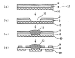
또 특허문헌 2에는, 도전성 페이스트를 사용하지 않고, 전기 도금에 의해 블라인드 비아 홀내에 금속을 석출시키는 다층 프린트 배선판의 제조 방법이 기재되어 있다. 도 3은 이 다층 프린트 배선판의 제조 프로세스를 나타내는 공정도이다.In addition,
우선, 기재(8)와, 기재(8)의 한쪽 면측에 형성된 제1 금속층(9)과, 다른쪽 면측에 형성된 제2 금속층(10)을 포함하는 기판(11)을 준비한 후(도 3a), 제1 금속층(9)과 기재(8)를 선택적으로 제거하여, 제2 금속층(10)에 도달하는 구멍(12)을 형성한다(도 3b). First, after preparing the board |
다음으로, 제2 금속층(10)으로부터 전력을 공급하여 전해 도금을 행하고, 구멍(12)의 내부에 금속을 석출시켜 구멍의 내부를 금속(13)으로 매립한다(도 3c). 그 후, 제1 금속층 및 제2 금속층을 에칭하여 배선 형성함으로써, 배선층을 2층 갖는 다층 프린트 배선 기판을 얻을 수 있다(도 3d). 제1 금속층의 에칭은 구멍(12) 의 형성전에 행할 수도 있다.Next, electric power is supplied from the
특허문헌 1 : 일본 특허공개 제2001-345555호 공보Patent Document 1: Japanese Patent Application Laid-Open No. 2001-345555
특허문헌 2 : 일본 특허공개 제2006-114787호 공보Patent Document 2: Japanese Patent Application Laid-Open No. 2006-114787
(발명의 개시)(Initiation of invention)
(발명이 해결하고자 하는 과제)(Tasks to be solved by the invention)
도전성 페이스트는 금속 분말 등의 도전성 필러를 수지 바인더 중에 분산시킨 것이며, 수지를 용해하기 위한 용제를 포함하고 있다. 이 때문에, 도전성 페이스트를 도포한 후 가열이나 감압 등에 의해 용제를 제거하면 도전성 페이스트의 체적은 감소한다. 또 도전성 페이스트는 압축함으로써 도전성 필러의 충전률이 높아지고, 도전성이 향상된다. 이 때문에 블라인드 비아 홀 접속의 접속 신뢰성을 높이기 위해서는 블라인드 비아 홀의 체적보다 크게 도전성 페이스트를 도포해야 하며, 특허문헌 1과 같이, 절연성 기재 표면으로부터 도전성 페이스트가 돌출된 상태가 되도록 도전성 페이스트를 도포해야 한다.The conductive paste is obtained by dispersing conductive fillers such as metal powder in a resin binder, and contains a solvent for dissolving the resin. For this reason, the volume of the conductive paste decreases when the solvent is removed by heating, reduced pressure, or the like after applying the conductive paste. Moreover, by compressing an electrically conductive paste, the filling rate of an electrically conductive filler becomes high and electroconductivity improves. For this reason, in order to improve the connection reliability of a blind via hole connection, an electrically conductive paste should be apply | coated larger than the volume of a blind via hole, and like the
그러나, 특허문헌 1의 방법에서는, 박리 필름(4)의 접합과 박리가 필요하여, 공정이 복잡해진다. 또, 배선층(2)의 에칭과 금속 필름(7)의 에칭은 별개의 공정으로 행해야 한다. 배선층(2)과 금속 필름(7)과의 층간 접속성을 높이기 위해서는, 도전성 페이스트의 프레스시에 균등하게 가압해야 하며, 미리 에칭 처리한 금속 필름(7)을 사용할 수 없기 때문이다.However, in the method of
특허문헌 2의 방법에서는 박리 필름은 필요없다. 그러나, 전기 도금으로 금속을 석출시킬 때, 블라인드 비아 홀의 하부로부터 성장한 도금이 제1 금속층(9)의 표면에 접촉하면, 제1 금속층(9)에도 전력이 공급되어 제1 금속층(9)의 표면에 금속이 석출하여 제1 금속층(9)의 두께가 두꺼워져, 세선 배선의 형성이 어려워진다. 이것을 방지하기 위해 제1 금속층(9)의 표면에 피복층을 형성할 수 있지만, 그만큼 공정이 복잡해진다. 또 제2 금속층(10)으로부터 전력을 공급하여 전기 도금을 행하기 위해서는 제2 금속층(10)이 연속되어 있어야 하여, 블라인드 비아 홀의 형성전에 제2 금속층(10)을 에칭하여 배선 형성하는 것은 어렵다.In the method of
본 발명은 상기 문제를 감안하여, 접속 신뢰성이 우수한 다층 프린트 배선판을 간단한 공정으로 제조할 수 있는, 생산성이 높은 다층 프린트 배선판의 제조 방법을 제공하는 것을 목적으로 한다. 또, 접속 신뢰성이 우수한 다층 프린트 배선판을 제공하는 것을 목적으로 한다.In view of the above problems, an object of the present invention is to provide a method for producing a highly productive multilayer printed wiring board that can produce a multilayer printed wiring board having excellent connection reliability in a simple step. Moreover, it aims at providing the multilayer printed wiring board which is excellent in connection reliability.
(발명을 해결하기 위한 수단)(Means for solving the invention)
본 발명은, (1) 기재, 상기 기재의 한쪽 표면상에 형성된 제1 도전층, 및 상기 기재의 다른쪽 표면상에 형성된 제2 도전층을 갖는 양면 기판을 준비하는 공정, (2) 상기 제1 도전층 및 상기 제2 도전층을 선택적으로 제거하여 배선 형성하는 공정, (3) 상기 기재를 선택적으로 제거함으로써, 상기 제2 도전층을 바닥면으로 하고, 상기 기재 및 상기 제1 도전층을 벽면으로 하는 블라인드 비아 홀을 형성하는 공정, (4) 상기 블라인드 비아 홀의 외주인 제1 도전층 표면과 상기 블라인드 비아 홀의 바닥면에 연속하도록 도전성 페이스트를 도포하는 공정을 가지며, 상기 제1 도전층과 상기 제2 도전층을 전기적으로 접속하는 다층 프린트 배선판의 제조 방법이다(청구항 1). The present invention provides a step of preparing a double-sided substrate having (1) a substrate, a first conductive layer formed on one surface of the substrate, and a second conductive layer formed on the other surface of the substrate, (2) the agent Selectively removing the first conductive layer and the second conductive layer to form a wiring, and (3) selectively removing the substrate to form the second conductive layer as a bottom surface, and to form the substrate and the first conductive layer. Forming a blind via hole having a wall surface; and (4) applying a conductive paste to the surface of the first conductive layer that is the outer circumference of the blind via hole and the bottom surface of the blind via hole. It is a manufacturing method of the multilayer printed wiring board which electrically connects a said 2nd conductive layer (claim 1).
도 4는 본 발명의 다층 프린트 배선판의 제조 방법의 일례를 나타내는 공정도이다. 기재(14), 상기 기재의 한쪽 표면상에 형성된 제1 도전층(15) 및 상기 기재의 다른쪽 표면상에 형성된 제2 도전층(16)을 갖는 양면 기판(17)을 준비한다(도 4a). 다음으로, 에칭 등의 방법으로 제1 도전층(15) 및 제2 도전층(16)을 선택적으로 제거하여 배선 형성한다(도 4b). It is process drawing which shows an example of the manufacturing method of the multilayer printed wiring board of this invention. A double-
다음으로 기재(14)를 선택적으로 제거하여 블라인드 비아 홀(18)을 형성한다. 블라인드 비아 홀(18)은, 제2 도전층(16)을 바닥면으로 하고, 기재(14) 및 제1 도전층(15)을 벽면으로 하고 있다. 또한, 형성된 블라인드 비아 홀에 도전성 페이스트(19)를 도포한다. 도 4d에 나타낸 바와 같이, 도전성 페이스트는 블라인드 비아 홀(18)의 외주인 제1 도전층(15)의 표면과, 블라인드 비아 홀의 바닥면에 연속하도록 도포된다. 그 후, 필요에 따라 도전성 페이스트(19)를 가열하여 경화시킨다. 도전성 페이스트를 프레스하면서 경화시켜도 된다. 이상의 공정에 의해 제1 도전층(15)과 제2 도전층(16)을 전기적으로 접속한다.Next, the
도전성 페이스트를 블라인드 비아 홀의 외주인 제1 도전층(15)의 표면에도 도포하기 때문에, 블라인드 비아 홀의 벽면만이 아니라, 제1 도전층(15)의 표면도 제2 도전층(16)과 접속하게 된다. 따라서 블라인드 비아 홀의 도전성이 향상되어, 접속 신뢰성이 우수한 다층 프린트 배선판을 얻을 수 있다. 또한 박리 필름의 접합이나 박리와 같은 공정을 필요로 하지 않아, 간단한 공정으로 다층 프린트 배선판을 제조할 수 있게 된다.Since the conductive paste is also applied to the surface of the first
또, 제1 도전층(15)과 제2 도전층(16)의 배선 형성을 한 후에 블라인드 비아 홀(18)을 형성할 수 있기 때문에, 제1 도전층(15)과 제2 도전층(16)을 동시에 에칭하여 배선 형성하는 것도 가능하다. 또한, 미리 배선 형성함으로써, 도 4d에 나타내는 도전성 페이스트를 도포한 기판과 별도의 기판을 일괄 적층하여 3층 이상의 도전층을 갖는 다층 프린트 배선판을 제조하는 것도 가능하다. 다층 프린트 배선판이란, 도전층이 2층 이상 있는 프린트 배선판을 가리키며, 양면판도 포함하는 것으로 한다.In addition, since the via via
청구항 2에 기재된 발명은, 상기 블라인드 비아 홀의 직경이 30 ㎛ 이상 200 ㎛ 이하인 것을 특징으로 하는 청구항 1에 기재된 다층 프린트 배선판의 제조 방법이다. 상기 블라인드 비아 홀의 직경을 30 ㎛ 이상 200 ㎛ 이하로 함으로써, 접속 신뢰성과 고밀도 실장성을 양립시킬 수 있다. 상기 블라인드 비아 홀의 형상은 원형, 타원형 등 임의의 형상으로 할 수 있고, 원형 이외의 형상의 경우는, 개구부의 최대 길이를 블라인드 비아 홀의 직경으로 한다. Invention of
청구항 3에 기재된 발명은, 상기 도전성 페이스트의 도포는, 상기 블라인드 비아 홀의 외주 전체를 피복하도록 도포하는 것을 특징으로 하는, 청구항 1 또는 2에 기재된 다층 프린트 배선판의 제조 방법이다. 상기 블라인드 비아 홀의 외주 전체를 피복하도록 도전성 페이스트를 도포함으로써, 제1 도전층(15)과 제2 도전층(16)이 양호하게 접속하여, 접속 신뢰성이 우수한 다층 프린트 배선판을 얻을 수 있다.Invention of
청구항 4에 기재된 발명은, 상기 도전성 페이스트의 도포 직경을 A로 하고, 상기 블라인드 비아 홀의 직경을 B로 했을 때, A와 B의 차이가 20 ㎛ 이상 200 ㎛ 이하인 것을 특징으로 하는, 청구항 3에 기재된 다층 프린트 배선판의 제조 방법이다. 이와 같이 도전성 페이스트를 도포함으로써, 접속 신뢰성과 고밀도 배선을 양립시킬 수 있다. 도전성 페이스트의 도포 형상은 원형, 타원형 등 임의의 형상으로 할 수 있고, 원형 이외의 형상의 경우는, 도포부의 최대 길이를 도전성 페이스트의 도포 직경으로 한다.In the invention according to
청구항 5에 기재된 발명은, 상기 양면 기판의 적어도 한쪽 표면을 피복하는 절연층을 적층하는 공정을 더 포함하고, 상기 도전성 페이스트를 도포하는 공정후에, 상기 절연층을 적층하고, 그 후 프레스하여 상기 절연층을 상기 양면 배선 기판에 접착시키는 것을 특징으로 하는, 청구항 1∼4 중 어느 한 항에 기재된 다층 프린트 배선판의 제조 방법이다.The invention according to
도 5는, 청구항 5에 기재된 발명의 다층 프린트 배선판의 제조 방법의 일례를 나타내는 공정도이다. 절연성 기재(20)와 접착층(21)을 갖는 절연층(커버레이 필름; 22)을, 도전성 페이스트를 도포한 양면 기판(17)에 적층한다(도 5a). 필요에 따라, 적층전에 도전성 페이스트를 미리 가열, 건조한다. 그 후, 절연층과 양면 기판의 적층체를 프레스하면 접착층(21)에 의해 절연층이 양면 기판(17)에 접착된다. 프레스는 가열 조건으로 행해지는 경우가 많아, 이 공정에 의해 도전성 페이스트의 열경화와 절연층의 접착을 한번에 행할 수 있다. 따라서 생산성이 우수한 다층 프린트 배선판의 제조 방법을 제공할 수 있다. 절연층(커버레이 필름)은 양면 기판(17)의 반대측(제2 도전층(16)을 피복하는 측)에 적층해도 되고, 또 양면에 적층하여 동시에 프레스하는 것도 가능하다. 이 경우는 생산성이 더욱 향상된다.FIG. 5 is a flowchart showing an example of a method of manufacturing the multilayer printed wiring board of the invention according to
청구항 6에 기재된 발명은, 기재, 상기 기재의 한쪽 표면상에 형성된 제1 도전층 및 상기 기재의 다른쪽 표면상에 형성된 제2 도전층을 가지며, 상기 제1 도전층과 상기 제2 도전층이 도전성 페이스트의 경화물로 전기적으로 접속되어 있는 다층 프린트 배선판으로서, 상기 제2 도전층을 바닥면으로 하고, 상기 기재 및 상기 제1 도전층을 벽면으로 하는 블라인드 비아 홀을 가지며, 상기 블라인드 비아 홀의 외주인 제1 도전층 표면과, 상기 블라인드 비아 홀의 바닥면에 연속하도록 도전성 페이스트의 경화물로 피복되어 있는 것을 특징으로 하는 다층 프린트 배선판이다. 상기 블라인드 비아 홀의 외주인 제1 도전층 표면과, 상기 블라인드 비아 홀의 바닥면에 연속하도록 도전성 페이스트의 경화물로 피복되어 있기 때문에, 제1 도전층과 제2 도전층이 양호하게 접속하여, 접속 신뢰성이 우수한 다층 프린트 배선판을 얻을 수 있다.Invention of
(발명의 효과)(Effects of the Invention)
본 발명은 접속 신뢰성이 우수한 다층 프린트 배선판을 간단한 공정으로 제조할 수 있는, 생산성이 높은 다층 프린트 배선판의 제조 방법을 제공한다. 또한, 접속 신뢰성이 우수한 다층 프린트 배선판을 제공한다.This invention provides the manufacturing method of the high productivity multilayer printed wiring board which can manufacture the multilayer printed wiring board which is excellent in connection reliability by a simple process. Moreover, the multilayer printed wiring board which is excellent in connection reliability is provided.
도 1은 종래의 다층 프린트 배선 기판의 제조 공정을 나타내는 단면 모식도이다. BRIEF DESCRIPTION OF THE DRAWINGS It is a cross-sectional schematic diagram which shows the manufacturing process of the conventional multilayer printed wiring board.
도 2는 종래의 다층 프린트 배선 기판의 제조 공정을 나타내는 단면 모식도 이다. 2 is a schematic cross-sectional view showing a step of manufacturing a conventional multilayer printed wiring board.
도 3은 종래의 다층 프린트 배선 기판의 제조 공정을 나타내는 단면 모식도이다. It is a cross-sectional schematic diagram which shows the manufacturing process of the conventional multilayer printed wiring board.
도 4는 본 발명의 다층 프린트 배선 기판의 제조 공정을 나타내는 단면 모식도이다. It is a cross-sectional schematic diagram which shows the manufacturing process of the multilayer printed wiring board of this invention.
도 5는 본 발명의 다층 프린트 배선 기판의 제조 공정을 나타내는 단면 모식도이다. It is a cross-sectional schematic diagram which shows the manufacturing process of the multilayer printed wiring board of this invention.
(부호의 설명)(Explanation of the sign)
1 : 절연성 기재 2 : 배선층1: Insulating base material 2: Wiring layer
3 : 편면 구리박 접착 기재 4 : 박리용 필름3: single-sided copper foil adhesive base material 4: peeling film
5 : 블라인드 비아 홀 6 : 도전성 페이스트5: blind via hole 6: conductive paste
7 : 금속 필름 8 : 기재7: metal film 8: base material
9 : 제1 금속층 10 : 제2 금속층9: first metal layer 10: second metal layer
11 : 기판 12 : 구멍11
13 : 금속 14 : 기재13
15 : 제1 도전층 16 : 제2 도전층15: first conductive layer 16: second conductive layer
17 : 양면 기판 18 : 블라인드 비아 홀17: double-sided substrate 18: blind via hole
19 : 도전성 페이스트 20 : 절연성 기재19: conductive paste 20: insulating base
21 : 접착층 22 : 절연층(커버레이 필름)21: adhesive layer 22: insulating layer (coverlay film)
(발명을 실시하기 위한 최선의 형태)(The best mode for carrying out the invention)
이하에 본 발명을 상세히 설명한다. 본 발명에 사용하는 기재로는 절연성의 수지 필름을 사용할 수 있고, 폴리에틸렌테레프탈레이트나 폴리이미드 등이 예시된다. 내열성을 고려하면 폴리이미드를 주체로 하는 수지 필름이 바람직하다. 기재의 두께는 다층 프린트 배선판의 용도에 따라 적절하게 선택할 수 있고, 일반적으로는 5 ㎛∼50 ㎛ 정도의 것을 사용한다.The present invention is described in detail below. An insulating resin film can be used as a base material used for this invention, Polyethylene terephthalate, a polyimide, etc. are illustrated. In consideration of heat resistance, a resin film mainly containing polyimide is preferable. The thickness of a base material can be suitably selected according to the use of a multilayer printed wiring board, and generally the thing of about 5 micrometers-50 micrometers is used.
제1 도전층 및 제2 도전층으로는 금속박을 사용할 수 있다. 도전성, 내구성을 고려하면 구리를 주체로 하는 금속박이 바람직하고, 구리, 또는 구리를 주성분으로 하는 합금이 예시된다. 구리 이외에도, 은, 알루미늄, 니켈 등을 사용해도 된다. 도전층의 두께는 다층 프린트 배선판의 용도에 따라 적절하게 선택할 수 있고, 일반적으로는 5 ㎛∼50 ㎛ 정도의 것을 사용한다. 도전층과 기재는 직접 또는 접착제를 통해 접합된다. 폴리이미드 수지 필름의 양면에 구리박이 접합된 시판하는 양면 구리 접착 기판을 사용해도 된다. Metal foil can be used as a 1st conductive layer and a 2nd conductive layer. In consideration of conductivity and durability, a metal foil mainly containing copper is preferable, and copper or an alloy mainly containing copper is exemplified. In addition to copper, you may use silver, aluminum, nickel, etc. The thickness of a conductive layer can be suitably selected according to the use of a multilayer printed wiring board, and generally 5 micrometers-about 50 micrometers are used. The conductive layer and the substrate are bonded directly or through an adhesive. You may use the commercially available double-sided copper adhesion board which copper foil was bonded to both surfaces of the polyimide resin film.
제1 도전층 및 제2 도전층을 에칭 가공 등에 의해 선택적으로 제거하여 배선 형성을 행한다. 에칭 가공으로는, 도전층상에 레지스트층 등의 배선 패턴을 형성한 후, 도전층을 침식하는 에칭제(echant)에 침지하여 배선 패턴 이외의 부분을 제거하고, 그 후 레지스트층을 제거하는 화학 에칭(침식 에칭)이 예시된다. 제1 도전층과 제2 도전층을 동시에 에칭 가공하면 에칭 공정을 1회로 할 수 있어, 제조 비용을 저감할 수 있다. The first conductive layer and the second conductive layer are selectively removed by etching or the like to form wiring. In etching, after forming a wiring pattern such as a resist layer on the conductive layer, the chemical etching is performed by immersing the conductive layer in an etchant that erodes the conductive layer to remove portions other than the wiring pattern, and then removing the resist layer. (Erosion etching) is illustrated. When the first conductive layer and the second conductive layer are etched simultaneously, the etching step can be performed once, and the manufacturing cost can be reduced.
배선 형성한 양면 기판에 레이저 가공 등의 방법으로 기재, 또는 기재와 제1 도전층을 선택적으로 제거하여, 블라인드 비아 홀을 형성한다. 레이저 가공에는, UV-YAG 레이저, CO2 레이저 등의 레이저를 사용할 수 있고, 또 레이저 가공 이외의 방법으로 블라인드 비아 홀을 형성하는 것도 가능하다. 블라인드 비아 홀의 직경은 30 ㎛∼200 ㎛으로 하는 것이 바람직하다. 직경이 30 ㎛보다 작으면 접속 면적이 작아지고, 제1 도전층과 제2 도전층의 접속 저항이 커진다. 또 직경을 200 ㎛보다 크게 하면, 배선폭에 비해 비아 홀이 커져 고밀도 실장을 할 수 없게 된다. 더욱 바람직한 블라인드 비아 홀의 직경은 50 ㎛∼150 ㎛이다.The substrate or the substrate and the first conductive layer are selectively removed from the wiring-formed double-sided substrate by a method such as laser processing to form blind via holes. Laser machining, it is possible to use a laser, such as UV-YAG laser, CO 2 laser, it is also possible to form a blind via hole with a method other than laser processing. It is preferable that the diameter of a blind via hole is 30 micrometers-200 micrometers. When diameter is smaller than 30 micrometers, connection area will become small and the connection resistance of a 1st conductive layer and a 2nd conductive layer will become large. If the diameter is larger than 200 mu m, the via hole becomes larger than the wiring width, and high density mounting cannot be performed. More preferred blind via holes have a diameter of 50 µm to 150 µm.
레이저 가공후의 스미어 제거는, 알칼리와 과망간산칼륨에 의한 습식 디스미어, 블러스트 처리, 액중에 무기 입자를 분산시켜 행하는 웨트 블러스트 처리, 플라즈마 처리 등이 이용된다.Smear removal after laser processing uses wet desmear by alkali and potassium permanganate, a blast process, the wet blast process which disperse | distributes an inorganic particle in a liquid, a plasma process, etc. are used.
본 발명에 사용하는 도전성 페이스트는, 금속 분말 등의 도전성 필러를 바인더 수지 중에 분산시킨 것이다. 금속 종류는 백금, 금, 은, 구리, 팔라듐 등이 예시되지만, 그 중에서도 특히 은 분말이나 은코팅 구리 분말을 사용하면 우수한 도전성을 나타내기 때문에 바람직하다.The electrically conductive paste used for this invention disperse | distributes electroconductive fillers, such as metal powder, in binder resin. Platinum, gold, silver, copper, palladium, and the like are exemplified as the metal type, and among them, silver powder or silver-coated copper powder is particularly preferable because of excellent conductivity.
바인더 수지로는, 에폭시 수지, 페놀 수지, 폴리에스테르 수지, 폴리우레탄 수지, 아크릴 수지, 멜라민 수지, 폴리이미드 수지, 폴리아미드이미드 수지 등을 사용할 수 있다. 도전성 페이스트의 내열성을 고려하면 열경화성 수지를 사용하는 것이 바람직하고, 특히 에폭시 수지를 사용하는 것이 바람직하다. 에폭시 수지의 종류는 특히 한정되지 않지만, 비스페놀 A, F, S, AD 등을 골격으로 하는 비스페놀 형 에폭시 수지 등 외에, 나프탈렌형 에폭시 수지, 노볼락형 에폭시 수지, 비페닐형 에폭시 수지, 디시클로펜타디엔형 에폭시 수지 등이 예시된다. 또 고분자량 에폭시 수지인 페녹시 수지를 사용할 수도 있다.As the binder resin, an epoxy resin, a phenol resin, a polyester resin, a polyurethane resin, an acrylic resin, a melamine resin, a polyimide resin, a polyamideimide resin, or the like can be used. In consideration of the heat resistance of the conductive paste, it is preferable to use a thermosetting resin, and it is particularly preferable to use an epoxy resin. Although the kind of epoxy resin is not specifically limited, Naphthalene type epoxy resin, a novolak-type epoxy resin, a biphenyl type epoxy resin, dicyclopenta other than bisphenol type epoxy resin etc. which make bisphenol A, F, S, AD etc. frame | skeleton Diene type epoxy resin etc. are illustrated. Moreover, the phenoxy resin which is a high molecular weight epoxy resin can also be used.
바인더 수지는 용제에 용해하여 사용할 수 있고, 에스테르계, 에테르계, 케톤계, 에테르에스테르계, 알콜계, 탄화수소계, 아민계 등의 유기 용제를 용제로서 사용할 수 있다. 도전성 페이스트는 스크린 인쇄 등의 방법으로 블라인드 비아 홀에 충전되기 때문에, 인쇄성이 우수한 고비점 용제가 바람직하고, 구체적으로는 카르비톨아세테이트, 부틸카르비톨아세테이트 등이 특히 바람직하다. 또 이들 용제를 수 종류 조합하여 사용하는 것도 가능하다. 이들 재료를 3개 롤, 회전 교반 탈포기 등으로 혼합, 분산하여 균일한 상태로 하여 도전성 페이스트를 제작한다.The binder resin can be dissolved and used in a solvent, and organic solvents such as esters, ethers, ketones, ether esters, alcohols, hydrocarbons, and amines can be used as the solvent. Since the conductive paste is filled into the blind via hole by a method such as screen printing, a high boiling point solvent excellent in printability is preferable, and carbitol acetate, butyl carbitol acetate, and the like are particularly preferable. It is also possible to use a combination of several kinds of these solvents. These materials are mixed and dispersed with three rolls, a rotary stirring defoaming machine, etc., to make a uniform state, and an electrically conductive paste is produced.
상기 도전성 페이스트를 스크린 인쇄 등의 방법으로 도포하여, 상기 블라인드 비아 홀내에 도전성 페이스트를 충전한다. 상기 블라인드 비아 홀의 외주인 제1 도전층 표면과 상기 블라인드 비아 홀의 바닥면에 연속하도록 도전성 페이스트를 도포하면, 제1 도전층과 제2 도전층이 도전성 페이스트를 통해 전기적으로 접속한다. 도전성 페이스트가 블라인드 비아 홀의 외주 및 바닥면 모두를 피복하는 것이 바람직하지만, 전기적으로 접속할 수 있다면 일부 결여되어도 된다.The conductive paste is applied by a method such as screen printing to fill the blind via hole with the conductive paste. When the conductive paste is applied continuously to the surface of the first conductive layer, which is the outer circumference of the blind via hole, and the bottom surface of the blind via hole, the first conductive layer and the second conductive layer are electrically connected through the conductive paste. It is preferable that the conductive paste covers both the outer circumference and the bottom surface of the blind via hole, but may be partially lacking if it can be electrically connected.
도전성 페이스트는 블라인드 비아 홀의 외주 전체를 피복하도록 도포하면, 접속 신뢰성이 높아져 바람직하다. 또 도전성 페이스트의 도포 직경을 A로 하고, 상기 블라인드 비아 홀의 직경을 B로 했을 때, A와 B의 차이가 20 ㎛ 이상 200 ㎛ 이하로 하는 것이 바람직하다. 도전성 페이스트의 도포 직경이 이 값보다 작으면, 제1 도전층과 제2 도전층과의 접속 저항이 높아져, 접속 신뢰성이 낮아진다. 또 도전성 페이스트의 도포 직경이 이 값보다 크면, 배선에 비해 접속부가 커져, 고밀도 실장을 행하기 어렵다. 또한 도전성 페이스트가 블라인드 비아 홀의 내부 전체에 충전되도록 도포하면, 제1 도전층과 제2 도전층과의 접속 저항을 낮게 할 수 있다.When the conductive paste is applied so as to cover the entire outer circumference of the blind via hole, the connection reliability is high, which is preferable. Moreover, when the application diameter of an electrically conductive paste is set to A, and the diameter of the said blind via hole is set to B, it is preferable that the difference of A and B shall be 20 micrometers or more and 200 micrometers or less. When the coating diameter of an electrically conductive paste is smaller than this value, the connection resistance of a 1st conductive layer and a 2nd conductive layer will become high, and connection reliability will become low. Moreover, when the coating diameter of an electrically conductive paste is larger than this value, a connection part will become large compared with wiring and it is difficult to carry out high density mounting. In addition, when the conductive paste is applied so as to fill the entire inside of the blind via hole, the connection resistance between the first conductive layer and the second conductive layer can be lowered.
도포한 도전성 페이스트를 예비 건조하여, 도전성 페이스트 중에 포함되는 용제를 제거하는 것이 바람직하다. 도전성 페이스트 중의 잔류 용제를 제거하는 것으로, 블라인드 비아 홀내에서의 보이드 발생을 방지할 수 있어, 접속 저항치를 낮게 할 수 있다. 또, 감압 분위기 중에서 예비 건조를 행하면, 예비 건조 온도를 낮게 하더라도 효율적으로 용제를 제거할 수 있고, 예비 건조 중의 바인더 수지의 경화 반응을 억제할 수 있다.It is preferable to predry the apply | coated electrically conductive paste and to remove the solvent contained in an electrically conductive paste. By removing the residual solvent in the conductive paste, the generation of voids in the blind via hole can be prevented, and the connection resistance value can be made low. Moreover, if preliminary drying is performed in a reduced pressure atmosphere, a solvent can be removed efficiently even if the predrying temperature is low, and the hardening reaction of the binder resin during predrying can be suppressed.
그 후, 도전성 페이스트를 경화시킨다. 도전성 페이스트의 경화는 열경화가 일반적이지만, 자외선 경화 등의 방법으로 행할 수도 있다. 또 열가소성 수지를 바인더 수지로 한 도전성 페이스트의 경우는, 용제를 건조시키는 것만으로 페이스트가 고화되지만, 본 발명에서는 이러한 것도 도전성 페이스트의 경화물이라 칭한다.Thereafter, the conductive paste is cured. Although hardening of an electrically conductive paste is common in thermosetting, it can also be performed by methods, such as an ultraviolet curing. Moreover, in the case of the electrically conductive paste which made thermoplastic resin the binder resin, although the paste solidifies only by drying a solvent, this also calls hardened | cured material of an electrically conductive paste in this invention.
도전성 페이스트를 프레스하면서 경화시키면 도전성이 향상되어 바람직하다. 프레스함으로써 도전성 페이스트는 압축되고, 제1 도전층과 제2 도전층과의 접속 저항이 작아진다. 또 블라인드 비아 홀내에도 압축한 도전성 페이스트가 충전되게 된다.When the conductive paste is cured while pressing, the conductivity is improved, which is preferable. By pressing, the electrically conductive paste is compressed, and the connection resistance between a 1st conductive layer and a 2nd conductive layer becomes small. The compressed conductive paste is also filled in the blind via holes.
도전성 페이스트를 도포한 양면 기판만을 프레스하면, 블라인드 비아 홀을 통해 제1 도전층과 제2 도전층이 접속한 다층 프린트 배선판을 얻을 수 있다. 이 배선판과 다른 배선판을 적층하여 삼층 이상의 배선층을 갖는 다층 프린트 배선판을 작성할 수도 있다. 또 도전성 페이스트를 도포한 양면 기판의 한면 또는 양면에 절연층(커버레이 필름)을 적층하여, 커버레이 필름의 접착과 도전성 페이스트의 프레스를 한번에 행할 수도 있다.When only the double-sided board | substrate which apply | coated the electrically conductive paste is pressed, the multilayer printed wiring board which the 1st conductive layer and the 2nd conductive layer connected through the blind via hole can be obtained. This wiring board and another wiring board can be laminated | stacked, and the multilayer printed wiring board which has three or more wiring layers can also be created. Moreover, an insulating layer (coverlay film) can be laminated | stacked on one side or both sides of the double-sided board | substrate which apply | coated the conductive paste, and adhesion of a coverlay film and press of a conductive paste can also be performed at once.
프레스는 가열하에 행하는 것이 바람직하다. 또 진공 상태에서 가열 프레스하면, 도전성 페이스트 중의 보이드 발생을 방지할 수 있어 더욱 바람직하다. 가열 온도는 도전성 페이스트의 종류에 따라 적절히 선택할 수 있지만, 통상 100℃∼280℃이다.It is preferable to perform a press under heating. Moreover, when it heat-presses in a vacuum state, the void generation in an electrically conductive paste can be prevented, and it is more preferable. Although heating temperature can be suitably selected according to the kind of electroconductive paste, it is 100 degreeC-280 degreeC normally.
실시예Example
다음으로 발명을 실시예에 기초하여 설명한다. 단, 본 발명의 범위는 실시예에만 한정되는 것은 아니다.Next, an invention is demonstrated based on an Example. However, the scope of the present invention is not limited only to an Example.
(실시예 1)(Example 1)
폴리이미드 필름의 양면에, 접착제를 사용하지 않고 구리박을 접합시킨 양면 구리 접착 기판(폴리이미드 필름 두께 : 25 ㎛, 구리박 두께 : 12 ㎛)을 준비하고, 양면의 구리박을 에칭 가공하여 배선 형성했다. 또한, UV-YAG 레이저에 의해 바닥을 갖는 블라인드 비아 홀(개구 직경 100 ㎛)을 형성하여, 웨트 블러스트 처리를 실시했다. 블라인드 비아 홀을 1296개 형성했다.A double-sided copper adhesive substrate (polyimide film thickness: 25 µm, copper foil thickness: 12 µm) was prepared by bonding copper foil to both surfaces of the polyimide film without using an adhesive, and the copper foils on both sides were etched and wired. Formed. Furthermore, the blind via hole (opening diameter 100 micrometers) which has a bottom was formed by UV-YAG laser, and the wet blasting process was performed. 1296 blind via holes were formed.
비스페놀 A형 에폭시 수지(에폭시당량 7000∼8500) 70질량부와, 비스페놀 F형 에폭시 수지(에폭시당량 160∼170) 30질량부를 부틸카르비톨아세테이트에 용해했다. 여기에 이미다졸계의 잠재성 경화제 12질량부를 첨가하고, 또한 은 입자를 전체 고형분의 55 체적%가 되도록 첨가하여 도전성 페이스트를 제작했다.70 mass parts of bisphenol A-type epoxy resins (epoxy equivalent 7000-885), and 30 mass parts of bisphenol F-type epoxy resins (epoxy equivalent 160-170) were melt | dissolved in butyl carbitol acetate. 12 mass parts of imidazole series latent hardening | curing agents were added here, and also silver particle was added so that it might become 55 volume% of all solid content, and the electrically conductive paste was produced.
스크린 인쇄에 의해 도전성 페이스트를 각각의 블라인드 비아 홀에 충전했다. 도전성 페이스트는 블라인드 비아 홀 전체를 피복하도록 도포하고, 도포 직경은 150 ㎛로 했다. 그 후, 감압하(1.3 kPa 이하)에 70℃로 가열하여 예비 건조하고, 도전성 페이스트 중의 용제를 제거했다.The conductive paste was filled in each blind via hole by screen printing. The electrically conductive paste was apply | coated so that the whole blind via hole might be coat | covered, and application | coating diameter was 150 micrometers. Thereafter, the mixture was heated to 70 ° C. under reduced pressure (1.3 kPa or less), preliminarily dried to remove the solvent in the conductive paste.
도전성 페이스트를 도포한 양면 기판을 진공 프레스하여, 1296개의 비아 홀이 데이지 체인 구조로 접속된 다층 프린트 배선판을 제작했다. 프레스 조건은 온도 200℃, 압력 2.0 MPa이다.The double-sided board | substrate which apply | coated the electrically conductive paste was vacuum-pressed, and the multilayer printed wiring board which 1296 via holes were connected by the daisy chain structure was produced. Press conditions are the temperature of 200 degreeC, and pressure 2.0MPa.
(실시예 2)(Example 2)
도전성 페이스트를 도포한 양면 기판의 양면에, 커버레이 필름(두께 20 ㎛의 접착제층이 한면에 적층된 두께 12 ㎛의 폴리이미드 필름)을 적층하여, 진공 프레스를 행한 것 외에는 실시예 1과 동일한 조건으로, 1296개의 비아 홀이 데이지 체인 구조로 접속된 다층 프린트 배선판을 제작했다.The same conditions as in Example 1 except that a coverlay film (a polyimide film having a thickness of 12 µm in which an adhesive layer having a thickness of 20 µm was laminated on one side) was laminated on both surfaces of the double-sided substrate coated with the conductive paste, and subjected to a vacuum press. As a result, a multilayer printed wiring board in which 1296 via holes were connected in a daisy chain structure was produced.
(실시예 3)(Example 3)
도전성 페이스트를 도포한 양면 기판의 양면에, 커버레이 필름(두께 20 ㎛의 접착제층이 한면에 적층된 두께 12 ㎛의 폴리이미드 필름)을 적층하고, 도전성 페이스트의 도포 직경을 100 ㎛로 하여, 진공 프레스를 행한 것 외에는 실시예 1과 동일한 조건으로, 1296개의 비아 홀이 데이지 체인 구조로 접속된 다층 프린트 배선판을 제작했다. On both sides of the double-sided substrate to which the conductive paste was applied, a coverlay film (polyimide film having a thickness of 12 μm in which an adhesive layer having a thickness of 20 μm was laminated on one side) was laminated, and the coating diameter of the conductive paste was set to 100 μm and vacuumed. A multilayered printed circuit board was fabricated in which 1296 via holes were connected in a daisy chain structure on the same conditions as in Example 1 except that pressing was performed.
(실시예 4)(Example 4)
도전성 페이스트를 도포한 양면 기판의 양면에, 커버레이 필름(두께 20 ㎛의 접착제층이 한면에 적층된 두께 12 ㎛의 폴리이미드 필름)을 적층하고, 도전성 페이스트의 도포 직경을 350 ㎛으로 하여 진공 프레스를 행한 것 외에는 실시예 1과 동일한 조건으로, 1296개의 비아 홀이 데이지 체인 구조로 접속된 다층 프린트 배선판을 제작했다.A coverlay film (12 μm thick polyimide film having an adhesive layer having a thickness of 20 μm laminated on one side) was laminated on both surfaces of the double-sided substrate on which the conductive paste was applied, and the vacuum paste was pressed at a coating diameter of 350 μm. A multilayer printed wiring board was produced in which 1296 via holes were connected in a daisy chain structure, except that the following conditions were carried out.
(접속 저항의 평가)(Evaluation of connection resistance)
얻어진 다층 프린트 배선판에 대해 접속 저항을 측정했다. 측정은 데이지 체인의 양단으로부터, 4단자법으로 저항을 측정함으로써 실시했다. 저항치는 1296개의 비아 홀내에 충전된 도전성 페이스트의 저항, 도전층의 저항 및 도전성 페이스트와 도전층의 접촉 저항의 합계라고 생각된다.Connection resistance was measured about the obtained multilayer printed wiring board. The measurement was performed by measuring resistance by the 4-terminal method from both ends of a daisy chain. The resistance value is considered to be the sum of the resistance of the conductive paste filled in 1296 via holes, the resistance of the conductive layer, and the contact resistance of the conductive paste and the conductive layer.
(신뢰성 평가)(Reliability assessment)
또한, 다층 프린트 배선판을 피크 온도 260℃의 리플로우로에 6회 통과시킨 후 접속 저항을 측정하여 저항 상승률을 구했다.Furthermore, after passing the multilayer printed wiring board through the reflow furnace of the peak temperature of 260
표 1에서 알 수 있는 바와 같이, 실시예 1∼4의 다층 프린트 배선판은 리플로우후의 저항 상승률이 5% 이하로 낮아, 접속 신뢰성이 우수하다는 것을 알 수 있다.As can be seen from Table 1, it can be seen that the multilayer printed wiring boards of Examples 1 to 4 have a low resistance increase rate after reflow of 5% or less, which is excellent in connection reliability.
Claims (6)
Applications Claiming Priority (2)
| Application Number | Priority Date | Filing Date | Title |
|---|---|---|---|
| JPJP-P-2006-285140 | 2006-10-19 | ||
| JP2006285140A JP2008103548A (en) | 2006-10-19 | 2006-10-19 | Multilayer printed wiring board, and its manufacturing method |
Publications (1)
| Publication Number | Publication Date |
|---|---|
| KR20090068227A true KR20090068227A (en) | 2009-06-25 |
Family
ID=39313949
Family Applications (1)
| Application Number | Title | Priority Date | Filing Date |
|---|---|---|---|
| KR1020097006805A KR20090068227A (en) | 2006-10-19 | 2007-10-12 | Multilayer printed wiring board and method for manufacturing the same |
Country Status (5)
| Country | Link |
|---|---|
| JP (1) | JP2008103548A (en) |
| KR (1) | KR20090068227A (en) |
| CN (1) | CN101530014A (en) |
| TW (1) | TWI406619B (en) |
| WO (1) | WO2008047718A1 (en) |
Cited By (1)
| Publication number | Priority date | Publication date | Assignee | Title |
|---|---|---|---|---|
| US10237983B2 (en) | 2014-12-23 | 2019-03-19 | Sanmina Corporation | Method for forming hole plug |
Families Citing this family (10)
| Publication number | Priority date | Publication date | Assignee | Title |
|---|---|---|---|---|
| JP4763813B2 (en) * | 2009-03-03 | 2011-08-31 | 住友電気工業株式会社 | Multilayer printed wiring board and manufacturing method thereof |
| WO2012011165A1 (en) * | 2010-07-20 | 2012-01-26 | 住友電気工業株式会社 | Multilayer printed circuit board and manufacturing method therefor |
| KR101895416B1 (en) | 2011-12-23 | 2018-09-06 | 엘지이노텍 주식회사 | Print circuit board substrate and method ofmanufacturing the same |
| JP5793113B2 (en) * | 2012-06-08 | 2015-10-14 | 住友電気工業株式会社 | Flexible printed wiring board |
| CN103002673B (en) * | 2012-12-21 | 2015-11-04 | 景旺电子科技(龙川)有限公司 | A kind of manufacture method of aluminium base and line layer conduction panel |
| CN105307405A (en) * | 2014-05-29 | 2016-02-03 | 景硕科技股份有限公司 | Method for fabricating circuit board etched by polyimide |
| EP3238512A4 (en) * | 2014-12-23 | 2018-08-22 | Sanmina Corporation | Hole plug for thin laminate |
| US10149392B2 (en) * | 2015-02-16 | 2018-12-04 | Nippo Mektron, Ltd. | Manufacturing method of flexible printed wiring board |
| JP7004921B2 (en) * | 2019-04-26 | 2022-01-21 | 日亜化学工業株式会社 | Light emitting module manufacturing method and light emitting module |
| CN114980521A (en) * | 2022-06-06 | 2022-08-30 | 北京梦之墨科技有限公司 | Electronic structure and manufacturing method thereof |
Family Cites Families (7)
| Publication number | Priority date | Publication date | Assignee | Title |
|---|---|---|---|---|
| JPH04199782A (en) * | 1990-11-29 | 1992-07-20 | Sharp Corp | Forming method for through hole of flexible board |
| JP2001024323A (en) * | 1999-07-12 | 2001-01-26 | Ibiden Co Ltd | Method for filling conductive paste and manufacture of single sided circuit board for multilayer printed wiring board |
| JP3892209B2 (en) * | 2000-06-22 | 2007-03-14 | 大日本印刷株式会社 | Printed wiring board and manufacturing method thereof |
| JPWO2003009660A1 (en) * | 2001-07-18 | 2004-11-11 | 松下電器産業株式会社 | Method for manufacturing circuit-formed substrate and material for manufacturing circuit-formed substrate |
| JP2003031917A (en) * | 2001-07-19 | 2003-01-31 | Fujikura Ltd | Structure for embedding conductive paste in blind hole of circuit board |
| JP4468081B2 (en) * | 2004-06-10 | 2010-05-26 | 三菱樹脂株式会社 | Conductive paste composition for multilayer wiring board |
| JP2006287019A (en) * | 2005-04-01 | 2006-10-19 | Hitachi Metals Ltd | Substrate with through-electrode and its manufacturing method |
-
2006
- 2006-10-19 JP JP2006285140A patent/JP2008103548A/en active Pending
-
2007
- 2007-10-12 WO PCT/JP2007/069976 patent/WO2008047718A1/en active Application Filing
- 2007-10-12 KR KR1020097006805A patent/KR20090068227A/en not_active Application Discontinuation
- 2007-10-12 CN CNA2007800389997A patent/CN101530014A/en active Pending
- 2007-10-17 TW TW096138824A patent/TWI406619B/en active
Cited By (2)
| Publication number | Priority date | Publication date | Assignee | Title |
|---|---|---|---|---|
| US10237983B2 (en) | 2014-12-23 | 2019-03-19 | Sanmina Corporation | Method for forming hole plug |
| US11246226B2 (en) | 2014-12-23 | 2022-02-08 | Sanmina Corporation | Laminate structures with hole plugs and methods of forming laminate structures with hole plugs |
Also Published As
| Publication number | Publication date |
|---|---|
| TW200829115A (en) | 2008-07-01 |
| WO2008047718A1 (en) | 2008-04-24 |
| CN101530014A (en) | 2009-09-09 |
| JP2008103548A (en) | 2008-05-01 |
| TWI406619B (en) | 2013-08-21 |
Similar Documents
| Publication | Publication Date | Title |
|---|---|---|
| KR20090068227A (en) | Multilayer printed wiring board and method for manufacturing the same | |
| EP1180920B1 (en) | Method of manufacturing a circuit board | |
| KR19990013967A (en) | Wiring board and manufacturing method thereof | |
| JPH0494186A (en) | Manufacture of multilayer circuit board | |
| JP5077800B2 (en) | Manufacturing method of multilayer printed wiring board | |
| JP3428070B2 (en) | Manufacturing method of printed wiring board | |
| JPH1117341A (en) | Frinted multilayer wiring board | |
| KR101281898B1 (en) | Multilayer printed wiring board and method for producing same | |
| JP6058321B2 (en) | Wiring board manufacturing method | |
| JP3705370B2 (en) | Manufacturing method of multilayer printed wiring board | |
| JPH08316598A (en) | Printed wiring board and production thereof | |
| WO2017213085A1 (en) | Method for manufacturing multilayer wiring board | |
| JP3738536B2 (en) | Method for manufacturing printed wiring board | |
| JPH09246728A (en) | Material for multilayer wiring board, manufacturing method thereof, and manufacturing method of multilayer wiring board, using it | |
| JPS63241995A (en) | Multilayer printed circuit board and manufacture of the same | |
| JP5429646B2 (en) | Method for manufacturing double-sided printed wiring board | |
| JP2008181914A (en) | Multilayer printed-wiring board and manufacturing method thereof | |
| KR100733814B1 (en) | Manufacturing method of pcb | |
| JP2007335631A (en) | Manufacturing method of laminated wiring board | |
| JP4821276B2 (en) | Multilayer printed wiring board manufacturing method and multilayer printed wiring board | |
| JP2008181915A (en) | Multilayer printed-wiring board and manufacturing method thereof | |
| JP3238901B2 (en) | Multilayer printed wiring board and method of manufacturing the same | |
| JP2001144445A (en) | Method for producing multilayer printed wiring board | |
| JPH09181452A (en) | Multilayer printed wiring board manufacturing method | |
| JP3855670B2 (en) | Multilayer circuit board manufacturing method |
Legal Events
| Date | Code | Title | Description |
|---|---|---|---|
| A201 | Request for examination | ||
| E902 | Notification of reason for refusal | ||
| E601 | Decision to refuse application | ||
| J201 | Request for trial against refusal decision | ||
| J301 | Trial decision |
Free format text: TRIAL DECISION FOR APPEAL AGAINST DECISION TO DECLINE REFUSAL REQUESTED 20140415 Effective date: 20140923 |