KR20070037848A - Organic light emitting diode display - Google Patents
Organic light emitting diode display Download PDFInfo
- Publication number
- KR20070037848A KR20070037848A KR1020050092940A KR20050092940A KR20070037848A KR 20070037848 A KR20070037848 A KR 20070037848A KR 1020050092940 A KR1020050092940 A KR 1020050092940A KR 20050092940 A KR20050092940 A KR 20050092940A KR 20070037848 A KR20070037848 A KR 20070037848A
- Authority
- KR
- South Korea
- Prior art keywords
- light emitting
- pixel
- driving transistor
- electrode
- pixels
- Prior art date
Links
Images


Classifications
-
- H—ELECTRICITY
- H05—ELECTRIC TECHNIQUES NOT OTHERWISE PROVIDED FOR
- H05B—ELECTRIC HEATING; ELECTRIC LIGHT SOURCES NOT OTHERWISE PROVIDED FOR; CIRCUIT ARRANGEMENTS FOR ELECTRIC LIGHT SOURCES, IN GENERAL
- H05B33/00—Electroluminescent light sources
- H05B33/12—Light sources with substantially two-dimensional radiating surfaces
- H05B33/20—Light sources with substantially two-dimensional radiating surfaces characterised by the chemical or physical composition or the arrangement of the material in which the electroluminescent material is embedded
-
- G—PHYSICS
- G09—EDUCATION; CRYPTOGRAPHY; DISPLAY; ADVERTISING; SEALS
- G09G—ARRANGEMENTS OR CIRCUITS FOR CONTROL OF INDICATING DEVICES USING STATIC MEANS TO PRESENT VARIABLE INFORMATION
- G09G3/00—Control arrangements or circuits, of interest only in connection with visual indicators other than cathode-ray tubes
- G09G3/20—Control arrangements or circuits, of interest only in connection with visual indicators other than cathode-ray tubes for presentation of an assembly of a number of characters, e.g. a page, by composing the assembly by combination of individual elements arranged in a matrix no fixed position being assigned to or needed to be assigned to the individual characters or partial characters
- G09G3/2007—Display of intermediate tones
- G09G3/2074—Display of intermediate tones using sub-pixels
-
- G—PHYSICS
- G09—EDUCATION; CRYPTOGRAPHY; DISPLAY; ADVERTISING; SEALS
- G09G—ARRANGEMENTS OR CIRCUITS FOR CONTROL OF INDICATING DEVICES USING STATIC MEANS TO PRESENT VARIABLE INFORMATION
- G09G3/00—Control arrangements or circuits, of interest only in connection with visual indicators other than cathode-ray tubes
- G09G3/20—Control arrangements or circuits, of interest only in connection with visual indicators other than cathode-ray tubes for presentation of an assembly of a number of characters, e.g. a page, by composing the assembly by combination of individual elements arranged in a matrix no fixed position being assigned to or needed to be assigned to the individual characters or partial characters
- G09G3/22—Control arrangements or circuits, of interest only in connection with visual indicators other than cathode-ray tubes for presentation of an assembly of a number of characters, e.g. a page, by composing the assembly by combination of individual elements arranged in a matrix no fixed position being assigned to or needed to be assigned to the individual characters or partial characters using controlled light sources
- G09G3/30—Control arrangements or circuits, of interest only in connection with visual indicators other than cathode-ray tubes for presentation of an assembly of a number of characters, e.g. a page, by composing the assembly by combination of individual elements arranged in a matrix no fixed position being assigned to or needed to be assigned to the individual characters or partial characters using controlled light sources using electroluminescent panels
- G09G3/32—Control arrangements or circuits, of interest only in connection with visual indicators other than cathode-ray tubes for presentation of an assembly of a number of characters, e.g. a page, by composing the assembly by combination of individual elements arranged in a matrix no fixed position being assigned to or needed to be assigned to the individual characters or partial characters using controlled light sources using electroluminescent panels semiconductive, e.g. using light-emitting diodes [LED]
- G09G3/3208—Control arrangements or circuits, of interest only in connection with visual indicators other than cathode-ray tubes for presentation of an assembly of a number of characters, e.g. a page, by composing the assembly by combination of individual elements arranged in a matrix no fixed position being assigned to or needed to be assigned to the individual characters or partial characters using controlled light sources using electroluminescent panels semiconductive, e.g. using light-emitting diodes [LED] organic, e.g. using organic light-emitting diodes [OLED]
- G09G3/3225—Control arrangements or circuits, of interest only in connection with visual indicators other than cathode-ray tubes for presentation of an assembly of a number of characters, e.g. a page, by composing the assembly by combination of individual elements arranged in a matrix no fixed position being assigned to or needed to be assigned to the individual characters or partial characters using controlled light sources using electroluminescent panels semiconductive, e.g. using light-emitting diodes [LED] organic, e.g. using organic light-emitting diodes [OLED] using an active matrix
-
- H—ELECTRICITY
- H05—ELECTRIC TECHNIQUES NOT OTHERWISE PROVIDED FOR
- H05B—ELECTRIC HEATING; ELECTRIC LIGHT SOURCES NOT OTHERWISE PROVIDED FOR; CIRCUIT ARRANGEMENTS FOR ELECTRIC LIGHT SOURCES, IN GENERAL
- H05B33/00—Electroluminescent light sources
- H05B33/12—Light sources with substantially two-dimensional radiating surfaces
-
- H—ELECTRICITY
- H10—SEMICONDUCTOR DEVICES; ELECTRIC SOLID-STATE DEVICES NOT OTHERWISE PROVIDED FOR
- H10K—ORGANIC ELECTRIC SOLID-STATE DEVICES
- H10K59/00—Integrated devices, or assemblies of multiple devices, comprising at least one organic light-emitting element covered by group H10K50/00
- H10K59/10—OLED displays
- H10K59/12—Active-matrix OLED [AMOLED] displays
- H10K59/121—Active-matrix OLED [AMOLED] displays characterised by the geometry or disposition of pixel elements
- H10K59/1213—Active-matrix OLED [AMOLED] displays characterised by the geometry or disposition of pixel elements the pixel elements being TFTs
-
- H—ELECTRICITY
- H10—SEMICONDUCTOR DEVICES; ELECTRIC SOLID-STATE DEVICES NOT OTHERWISE PROVIDED FOR
- H10K—ORGANIC ELECTRIC SOLID-STATE DEVICES
- H10K59/00—Integrated devices, or assemblies of multiple devices, comprising at least one organic light-emitting element covered by group H10K50/00
- H10K59/30—Devices specially adapted for multicolour light emission
- H10K59/38—Devices specially adapted for multicolour light emission comprising colour filters or colour changing media [CCM]
-
- G—PHYSICS
- G09—EDUCATION; CRYPTOGRAPHY; DISPLAY; ADVERTISING; SEALS
- G09G—ARRANGEMENTS OR CIRCUITS FOR CONTROL OF INDICATING DEVICES USING STATIC MEANS TO PRESENT VARIABLE INFORMATION
- G09G2320/00—Control of display operating conditions
- G09G2320/02—Improving the quality of display appearance
- G09G2320/0233—Improving the luminance or brightness uniformity across the screen
-
- G—PHYSICS
- G09—EDUCATION; CRYPTOGRAPHY; DISPLAY; ADVERTISING; SEALS
- G09G—ARRANGEMENTS OR CIRCUITS FOR CONTROL OF INDICATING DEVICES USING STATIC MEANS TO PRESENT VARIABLE INFORMATION
- G09G2320/00—Control of display operating conditions
- G09G2320/04—Maintaining the quality of display appearance
- G09G2320/043—Preventing or counteracting the effects of ageing
Landscapes
- Engineering & Computer Science (AREA)
- Physics & Mathematics (AREA)
- Computer Hardware Design (AREA)
- General Physics & Mathematics (AREA)
- Theoretical Computer Science (AREA)
- Geometry (AREA)
- Microelectronics & Electronic Packaging (AREA)
- Devices For Indicating Variable Information By Combining Individual Elements (AREA)
- Electroluminescent Light Sources (AREA)
Abstract
본 발명은 게이트선 및 데이터선에 의해 정의되며 발광 소자 및 이와 연결되어 있는 구동 트랜지스터를 각각 포함하는 제1 화소, 제2 화소 및 제3 화소를 포함하며, 상기 제1 화소의 발광 소자는 상기 제2 화소 및 상기 제3 화소의 발광 소자보다 발광 효율이 낮으며, 상기 제1 화소, 상기 제2 화소 및 상기 제3 화소의 발광 소자는 실질적으로 동일한 면적을 가지며, 상기 제1 화소의 구동 트랜지스터가 차지하는 면적은 상기 제2 화소 또는 상기 제3 화소의 구동 트랜지스터가 차지하는 면적보다 큰 유기 발광 표시 장치에 대한 것이다.The present invention includes a first pixel, a second pixel, and a third pixel, each of which is defined by a gate line and a data line, and includes a light emitting device and a driving transistor connected thereto. The luminous efficiency is lower than that of the light emitting elements of the two pixels and the third pixel, and the light emitting elements of the first pixel, the second pixel and the third pixel have substantially the same area, and the driving transistor of the first pixel The area occupied by the organic light emitting diode display is larger than the area occupied by the driving transistor of the second pixel or the third pixel.
박막 트랜지스터, 발광 효율, 채널 폭, 보상 회로 Thin Film Transistors, Luminous Efficiency, Channel Width, Compensation Circuit
Description
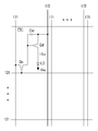
도 1은 본 발명의 한 실시예에 따른 유기 발광 표시 장치의 등가 회로도이고,1 is an equivalent circuit diagram of an organic light emitting diode display according to an exemplary embodiment of the present invention.
도 2, 도 3 및 도 4는 본 발명의 한 실시예에 따른 유기 발광 표시 장치에서 다른 세 개의 화소를 각각 보여주는 배치도이고, 2, 3, and 4 are layout views showing three different pixels in the organic light emitting diode display according to the exemplary embodiment.
도 5는 도 4의 유기 발광 표시 장치에서 하나의 화소를 V-V 선을 따라 잘라 도시한 단면도이고,FIG. 5 is a cross-sectional view of one pixel taken along the line V-V in the organic light emitting diode display of FIG. 4.
도 6은 본 발명의 한 실시예에 따른 유기 발광 표시 장치의 복수의 화소를 보여주는 배치도이고,6 is a layout view illustrating a plurality of pixels of an organic light emitting diode display according to an exemplary embodiment of the present disclosure.
도 7은 본 발명의 다른 한 실시예에 따른 유기 발광 표시 장치의 등가 회로도이고, 7 is an equivalent circuit diagram of an organic light emitting diode display according to another exemplary embodiment of the present invention.
도 8, 도 9 및 도 10은 본 발명의 다른 한 실시예에 따른 유기 발광 표시 장치에서 다른 세 개의 화소를 각각 보여주는 배치도이고,8, 9, and 10 are layout views showing three different pixels in the organic light emitting diode display according to another exemplary embodiment.
도 11은 도 9의 유기 발광 표시 장치에서 하나의 화소를 X-X 선을 따라 잘라 도시한 단면도이고,FIG. 11 is a cross-sectional view of one pixel taken along an X-X line in the OLED display of FIG. 9.
도 12는 본 발명의 다른 한 실시예에 따른 유기 발광 표시 장치의 복수의 화소를 보여주는 배치도이다. 12 is a layout view illustrating a plurality of pixels of an organic light emitting diode display according to another exemplary embodiment of the present invention.
본 발명은 유기 발광 표시 장치에 관한 것이다.The present invention relates to an organic light emitting display device.
최근 모니터 또는 텔레비전 등의 경량화 및 박형화가 요구되고 있으며, 이러한 요구에 따라 음극선관(cathode ray tube, CRT)이 액정 표시 장치(liquid crystal display, LCD)로 대체되고 있다.Recently, there is a demand for weight reduction and thinning of a monitor or a television, and according to such a demand, a cathode ray tube (CRT) has been replaced by a liquid crystal display (LCD).
그러나, 액정 표시 장치는 수발광 소자로서 별도의 백라이트(backlight)가 필요할 뿐만 아니라, 응답 속도 및 시야각 등에서 많은 문제점이 있다.However, the liquid crystal display device requires not only a separate backlight as a light emitting device, but also has many problems in response speed and viewing angle.
최근 이러한 문제점을 극복할 수 있는 표시 장치로서, 유기 발광 표시 장치(organic light emitting diode display, OLED display)가 주목받고 있다. Recently, as a display device capable of overcoming such a problem, an organic light emitting diode display (OLED display) has attracted attention.
유기 발광 표시 장치는 두 개의 전극과 그 사이에 위치하는 발광층을 포함하며, 하나의 전극으로부터 주입된 전자(electron)와 다른 전극으로부터 주입된 정공(hole)이 발광층에서 결합하여 여기자(exiton)를 형성하고, 여기자가 에너지를 방출하면서 발광한다.The organic light emitting diode display includes two electrodes and a light emitting layer interposed therebetween, and electrons injected from one electrode and holes injected from another electrode are combined in the light emitting layer to form an exciton. The excitons emit light while releasing energy.
유기 발광 표시 장치는 자체발광형으로 별도의 광원이 필요 없기 때문에 소비전력 측면에서 유리할 뿐만 아니라, 응답 속도, 시야각 및 대비비(contrast ratio)도 우수하다.The organic light emitting diode display is not only advantageous in terms of power consumption because it does not need a separate light source, and also has excellent response speed, viewing angle, and contrast ratio.
그러나 유기 발광 표시 장치는 적색, 녹색 및 청색의 발광 재료에 따라 발광 효율이 다르다. 따라서, 적색, 녹색 및 청색 발광을 동일하게 제어하기 위해서는 발광 효율이 가장 낮은 영역을 기준으로 화소가 설계되어야 하고, 이 경우 개구율이 크게 저하된다. However, the light emitting efficiency of the organic light emitting diode display varies depending on the red, green, and blue light emitting materials. Therefore, in order to control red, green and blue light emission equally, the pixel should be designed based on the region having the lowest luminous efficiency, and in this case, the aperture ratio is greatly reduced.
본 발명이 이루고자 하는 기술적 과제는 이러한 문제점을 해결하는 것으로서, 유기 발광 표시 장치의 전류 구동 특성을 확보하면서도 개구율을 높이는 것이다.The technical problem to be solved by the present invention is to solve such a problem, and to increase the aperture ratio while securing current driving characteristics of the organic light emitting diode display.
본 발명의 한 실시예에 따른 유기 발광 표시 장치는, 게이트선 및 데이터선에 의해 정의되며 발광 소자 및 이와 연결되어 있는 구동 트랜지스터를 각각 포함하는 제1 화소, 제2 화소 및 제3 화소를 포함하며, 상기 제1 화소의 발광 소자는 상기 제2 화소 및 상기 제3 화소의 발광 소자보다 발광 효율이 낮으며, 상기 제1 화소, 상기 제2 화소 및 상기 제3 화소의 발광 소자는 실질적으로 동일한 면적을 가지며, 상기 제1 화소의 구동 트랜지스터가 차지하는 면적은 상기 제2 화소 또는 상기 제3 화소의 구동 트랜지스터가 차지하는 면적보다 크다.An organic light emitting diode display according to an exemplary embodiment of the present invention includes a first pixel, a second pixel, and a third pixel, each of which is defined by a gate line and a data line and includes a light emitting element and a driving transistor connected thereto. The light emitting device of the first pixel has lower luminous efficiency than the light emitting device of the second pixel and the third pixel, and the light emitting devices of the first pixel, the second pixel, and the third pixel have substantially the same area. The area occupied by the driving transistor of the first pixel is larger than the area occupied by the driving transistor of the second pixel or the third pixel.
또한, 상기 제1 화소의 구동 트랜지스터의 채널은 상기 제2 및 제3 화소의 구동 트랜지스터의 채널과 다른 위치에 형성될 수 있다.In addition, the channel of the driving transistor of the first pixel may be formed at a position different from that of the driving transistor of the second and third pixels.
또한, 상기 제1 화소의 구동 트랜지스터의 채널은 상기 게이트선과 상기 발광 소자 사이에 위치하며, 상기 제2 및 제3 화소의 구동 트랜지스터의 채널은 상기 데이터선과 상기 발광 소자 사이에 위치할 수 있다.The channel of the driving transistor of the first pixel may be positioned between the gate line and the light emitting device, and the channel of the driving transistor of the second and third pixels may be located between the data line and the light emitting device.
또한, 상기 제1 화소의 구동 트랜지스터는 채널이 사행(蛇行)일 수 있다.In addition, the driving transistor of the first pixel may have a meandering channel.
또한, 상기 제1 화소의 구동 트랜지스터의 채널 폭은 상기 제2 및 제3 화소의 구동 트랜지스터의 채널 폭보다 넓을 수 있다.The channel width of the driving transistor of the first pixel may be wider than the channel width of the driving transistor of the second and third pixels.
또한, 상기 제1, 제2 및 제3 화소는 폭이 동일할 수 있다.In addition, the first, second and third pixels may have the same width.
또한, 상기 제1 화소는 청색 광을 방출할 수 있다.In addition, the first pixel may emit blue light.
또한, 상기 구동 트랜지스터를 이루는 반도체는 비정질 규소를 포함할 수 있다.In addition, the semiconductor constituting the driving transistor may include amorphous silicon.
또한, 상기 제1, 제2 및 제3 화소는 상기 게이트선 및 상기 데이터선과 연결되어 있는 스위칭 트랜지스터를 더 포함할 수 있다.The first, second and third pixels may further include a switching transistor connected to the gate line and the data line.
또한, 상기 제1, 제2 및 제3 화소에 각각 포함되어 있는 발광 소자는 상기 구동 트랜지스터에 연결되어 있는 화소 전극, 상기 화소 전극과 마주보는 공통 전극, 그리고 상기 화소 전극과 상기 공통 전극 사이에 끼어 있으며 제1, 제2 및 제3 발광 영역을 정의하는 제1, 제2 및 제3 유기 발광 부재를 각각 포함할 수 있다.The light emitting device included in each of the first, second, and third pixels may include a pixel electrode connected to the driving transistor, a common electrode facing the pixel electrode, and a gap between the pixel electrode and the common electrode. And first, second, and third organic light emitting members defining first, second, and third light emitting regions, respectively.
또한, 상기 제1 발광 영역은 상기 제2 및 제3 발광 영역과 폭과 길이가 다를 수 있다.In addition, the first emission area may have a width and a length different from those of the second and third emission areas.
또한, 상기 제1 발광 영역은 상기 제2 및 제3 발광 영역보다 폭이 넓고 길이가 짧을 수 있다.In addition, the first emission region may have a wider width and a shorter length than the second and third emission regions.
또한, 상기 제1 발광 영역과 상기 제1 발광 영역에 이웃하는 상기 제2 또는 제3 발광 영역 사이의 간격은 상기 제2 발광 영역과 상기 제3 발광 영역 사이의 간격보다 좁을 수 있다.In addition, an interval between the first emission region and the second or third emission region adjacent to the first emission region may be smaller than an interval between the second emission region and the third emission region.
또한, 상기 제1 유기 발광 부재는 청색 광을 방출할 수 있다.In addition, the first organic light emitting member may emit blue light.
본 발명의 한 실시예에 따른 유기 발광 표시 장치는, 발광 소자 및 이와 연결되어 있는 구동 트랜지스터를 각각 포함하며 제1, 제2 및 제3 발광 영역을 각각 가지는 제1 화소, 제2 화소 및 제3 화소를 포함하며, 상기 제1 화소의 발광 소자는 상기 제2 화소 및 상기 제3 화소의 발광 소자보다 발광 효율이 낮으며, 상기 제1 발광 영역은 상기 제2 및 제3 발광 영역과 폭과 길이가 다르며, 상기 제1, 제2 및 제3 발광 영역은 실질적으로 동일한 면적을 가진다.An organic light emitting diode display according to an exemplary embodiment of the present invention includes a light emitting element and a driving transistor connected thereto, and includes a first pixel, a second pixel, and a third pixel having first, second, and third light emitting regions, respectively. And a light emitting device of the first pixel, the light emitting efficiency of which is lower than that of the second pixel and the third pixel, and the first light emitting area has a width and a length of the second and third light emitting areas. Are different, and the first, second and third light emitting regions have substantially the same area.
또한, 상기 제1 발광 영역은 상기 제2 및 제3 발광 영역보다 폭이 넓고 길이가 짧을 수 있다.In addition, the first emission region may have a wider width and a shorter length than the second and third emission regions.
또한, 상기 제1 화소의 구동 트랜지스터의 채널은 상기 게이트선과 상기 발광 소자 사이에 위치하며, 상기 제2 및 제3 화소의 구동 트랜지스터의 채널은 상기 데이터선과 상기 발광 소자 사이에 위치할 수 있다.The channel of the driving transistor of the first pixel may be positioned between the gate line and the light emitting device, and the channel of the driving transistor of the second and third pixels may be located between the data line and the light emitting device.
또한, 상기 제1 발광 소자는 청색 광을 방출할 수 있다.In addition, the first light emitting device may emit blue light.
이하, 첨부한 도면을 참고로 하여 본 발명의 실시예에 대하여 본 발명이 속하는 기술 분야에서 통상의 지식을 가진 자가 용이하게 실시할 수 있도록 상세히 설명한다. 그러나 본 발명은 여러 가지 상이한 형태로 구현될 수 있으며 여기에서 설명하는 실시예에 한정되지 않는다.Hereinafter, exemplary embodiments of the present invention will be described in detail with reference to the accompanying drawings so that those skilled in the art may easily implement the present invention. As those skilled in the art would realize, the described embodiments may be modified in various different ways, all without departing from the spirit or scope of the present invention.
도면에서 여러 층 및 영역을 명확하게 표현하기 위하여 두께를 확대하여 나타내었다. 명세서 전체를 통하여 유사한 부분에 대해서는 동일한 도면 부호를 붙였다. 층, 막, 영역, 판 등의 부분이 다른 부분 "위에" 있다고 할 때, 이는 다른 부분 "바로 위에" 있는 경우뿐 아니라 그 중간에 또 다른 부분이 있는 경우도 포함 한다. 반대로 어떤 부분이 다른 부분 "바로 위에" 있다고 할 때에는 중간에 다른 부분이 없는 것을 뜻한다.In the drawings, the thickness of layers, films, panels, regions, etc., are exaggerated for clarity. Like parts are designated by like reference numerals throughout the specification. When a part of a layer, film, area, plate, etc. is said to be "on" another part, this includes not only the other part being "right over" but also another part in the middle. On the contrary, when a part is "just above" another part, there is no other part in the middle.
먼저 본 발명의 한 실시예에 따른 유기 발광 표시 장치에 대하여 도 1을 참고로 상세하게 설명한다.First, an organic light emitting diode display according to an exemplary embodiment of the present invention will be described in detail with reference to FIG. 1.
도 1은 본 발명의 한 실시예에 따른 유기 발광 표시 장치의 등가 회로도이다.1 is an equivalent circuit diagram of an organic light emitting diode display according to an exemplary embodiment of the present invention.
도 1을 참고하면, 본 실시예에 따른 유기 발광 표시 장치는 복수의 신호선(121, 171, 172)과 이들에 연결되어 있으며 대략 행렬(matrix)의 형태로 배열된 복수의 화소(pixel)(PX1)를 포함한다.Referring to FIG. 1, the organic light emitting diode display according to the present exemplary embodiment includes a plurality of
신호선은 게이트 신호(또는 주사 신호)를 전달하는 복수의 게이트선(gate line)(121), 데이터 신호를 전달하는 복수의 데이터선(data line)(171) 및 구동 전압을 전달하는 복수의 구동 전압선(driving voltage line)(172)을 포함한다. 게이트선(121)은 대략 행 방향으로 뻗어 있으며 서로가 거의 평행하고 데이터선(171)과 구동 전압선(172)은 대략 열 방향으로 뻗어 있으며 서로가 거의 평행하다.The signal line includes a plurality of
각 화소(PX)는 스위칭 트랜지스터(switching transistor)(Qs), 구동 트랜지스터(driving transistor)(Qd), 유지 축전기(storage capacitor)(Cst) 및 유기 발광 다이오드(organic light emitting diode, OLED)(LD)를 포함한다.Each pixel PX includes a switching transistor Qs, a driving transistor Qd, a storage capacitor Cst, and an organic light emitting diode OLED. It includes.
스위칭 트랜지스터(Qs)는 제어 단자(control terminal), 입력 단자(input terminal) 및 출력 단자(output terminal)를 가지는데, 제어 단자는 게이트선(121)에 연결되어 있고, 입력 단자는 데이터선(171)에 연결되어 있으며, 출력 단자는 구 동 트랜지스터(Qd)에 연결되어 있다. 스위칭 트랜지스터(Qs)는 게이트선(121)에 인가되는 주사 신호에 응답하여 데이터선(171)에 인가되는 데이터 신호를 구동 트랜지스터(Qd)에 전달한다.The switching transistor Qs has a control terminal, an input terminal, and an output terminal. The control terminal is connected to the
구동 트랜지스터(Qd) 또한 제어 단자, 입력 단자 및 출력 단자를 가지는데, 제어 단자는 스위칭 트랜지스터(Qs)에 연결되어 있고, 입력 단자는 구동 전압선(172)에 연결되어 있으며, 출력 단자는 유기 발광 다이오드(LD)에 연결되어 있다. 구동 트랜지스터(Qd)는 제어 단자와 출력 단자 사이에 걸리는 전압에 따라 그 크기가 달라지는 출력 전류(ILD)를 흘린다.The driving transistor Qd also has a control terminal, an input terminal and an output terminal, the control terminal being connected to the switching transistor Qs, the input terminal being connected to the
축전기(Cst)는 구동 트랜지스터(Qd)의 제어 단자와 입력 단자 사이에 연결되어 있다. 이 축전기(Cst)는 구동 트랜지스터(Qd)의 제어 단자에 인가되는 데이터 신호를 충전하고 스위칭 트랜지스터(Qs)가 턴 오프(turn-off)된 뒤에도 이를 유지한다.The capacitor Cst is connected between the control terminal and the input terminal of the driving transistor Qd. The capacitor Cst charges the data signal applied to the control terminal of the driving transistor Qd and maintains it even after the switching transistor Qs is turned off.
유기 발광 다이오드(LD)는 구동 트랜지스터(Qd)의 출력 단자에 연결되어 있는 애노드(anode)와 공통 전압(Vss)에 연결되어 있는 캐소드(cathode)를 가진다. 유기 발광 다이오드(LD)는 구동 트랜지스터(Qd)의 출력 전류(ILD)에 따라 세기를 달리하여 발광함으로써 영상을 표시한다.The organic light emitting diode LD has an anode connected to the output terminal of the driving transistor Qd and a cathode connected to the common voltage Vss. The organic light emitting diode LD displays an image by emitting light having a different intensity depending on the output current I LD of the driving transistor Qd.
스위칭 트랜지스터(Qs) 및 구동 트랜지스터(Qd)는 n-채널 전계 효과 트랜지스터(field effect transistor, FET)이다. 그러나 스위칭 트랜지스터(Qs)와 구동 트랜지스터(Qd) 중 적어도 하나는 p-채널 전계 효과 트랜지스터일 수 있다. 또한, 트랜지스터(Qs, Qd), 축전기(Cst) 및 유기 발광 다이오드(LD)의 연결 관계가 바뀔 수 있다.The switching transistor Qs and the driving transistor Qd are n-channel field effect transistors (FETs). However, at least one of the switching transistor Qs and the driving transistor Qd may be a p-channel field effect transistor. In addition, the connection relationship between the transistors Qs and Qd, the capacitor Cst, and the organic light emitting diode LD may be changed.
그러면, 도 1에 도시한 유기 발광 표시 장치의 상세 구조에 대하여 도 2 내지 도 5를 참조하여 상세하게 설명한다.Next, the detailed structure of the organic light emitting diode display illustrated in FIG. 1 will be described in detail with reference to FIGS. 2 to 5.
도 2, 도 3 및 도 4는 본 발명의 한 실시예에 따른 유기 발광 표시 장치에서 다른 세 개의 화소를 각각 보여주는 배치도이고, 도 5는 도 4의 유기 발광 표시 장치에서 하나의 화소를 V-V 선을 따라 잘라 도시한 단면도이다. 도 2 내지 도 5에서, 각 화소에서 대응되는 구성 요소는 동일한 도면 부호로 표시하였다.2, 3, and 4 are layout views showing three different pixels in the organic light emitting diode display according to an exemplary embodiment of the present invention, and FIG. 5 illustrates one pixel as a VV line in the organic light emitting diode display of FIG. 4. It is a cross-sectional view cut along. 2 to 5, corresponding components in each pixel are denoted by the same reference numerals.
투명한 유리 또는 플라스틱 따위로 만들어진 절연 기판(110) 위에 제1 제어 전극(control electrode)(124a)을 포함하는 복수의 게이트선(121) 및 복수의 제2 제어 전극(124b)을 포함하는 복수의 게이트 도전체(gate conductor)가 형성되어 있다.A plurality of gates including a plurality of
게이트선(121)은 게이트 신호를 전달하며 주로 가로 방향으로 뻗어 있다. 각 게이트선(121)은 다른 층 또는 외부 구동 회로와의 접속을 위하여 면적이 넓은 끝 부분(129)을 포함하며, 제1 제어 전극(124a)은 게이트선(121)으로부터 위로 뻗어 있다. 게이트 신호를 생성하는 게이트 구동 회로(도시하지 않음)가 기판(110) 위에 집적되어 있는 경우 게이트선(121)이 연장되어 게이트 구동 회로와 직접 연결될 수 있다.The
제2 제어 전극(124b)은 게이트선(121)과 분리되어 있다.The
게이트 도전체(121, 124b)는 알루미늄(Al)이나 알루미늄 합금 등 알루미늄 계열 금속, 은(Ag)이나 은 합금 등 은 계열 금속, 구리(Cu)나 구리 합금 등 구리 계열 금속, 몰리브덴(Mo)이나 몰리브덴 합금 등 몰리브덴 계열 금속, 크롬(Cr), 탄탈륨(Ta) 및 티타늄(Ti) 따위로 만들어질 수 있다. 그러나 이들은 물리적 성질이 다른 두 개의 도전막(도시하지 않음)을 포함하는 다중막 구조를 가질 수도 있다. 이 중 한 도전막은 신호 지연이나 전압 강하를 줄일 수 있도록 비저항(resistivity)이 낮은 금속, 예를 들면 알루미늄 계열 금속, 은 계열 금속, 구리 계열 금속 등으로 만들어진다. 이와는 달리, 다른 도전막은 다른 물질, 특히 ITO(indium tin oxide) 및 IZO(indium zinc oxide)와의 물리적, 화학적, 전기적 접촉 특성이 우수한 물질, 이를테면 몰리브덴 계열 금속, 크롬, 티타늄, 탄탈륨 등으로 만들어진다. 이러한 조합의 좋은 예로는 크롬 하부막과 알루미늄 (합금) 상부막 및 알루미늄 (합금) 하부막과 몰리브덴 (합금) 상부막을 들 수 있다. 그러나 게이트 도전체(121, 124b)는 이외에도 여러 가지 다양한 금속 또는 도전체로 만들어질 수 있다.The
게이트 도전체(121, 124b)의 측면은 기판(110) 면에 대하여 경사져 있으며 그 경사각은 약 30° 내지 약 80°인 것이 바람직하다. Side surfaces of the
게이트 도전체(121, 124b) 위에는 질화규소(SiNx) 또는 산화규소(SiOx) 따위로 만들어진 게이트 절연막(gate insulating layer)(140)이 형성되어 있다.A
게이트 절연막(140) 위에는 수소화 비정질 규소(hydrogenated amorphous silicon)(비정질 규소는 약칭 a-Si로 씀) 또는 다결정 규소(polysilicon) 등으로 만들어진 복수의 선형 반도체(151)와 섬형 반도체(154b)가 형성되어 있다. 선형 반도체(151)는 주로 세로 방향으로 뻗어 있으며 제1 제어 전극(124a)을 향하여 뻗어 나온 복수의 돌출부(projection)(154a)를 포함한다. 섬형 반도체(154b)는 제2 제어 전극(124b) 위에 위치한다.On the
선형 및 섬형 반도체(151, 154b) 위에는 각각 복수 쌍의 제1 저항성 접촉 부재(ohmic contact)(163a, 165a)와 복수 쌍의 제2 저항성 접촉 부재(163b, 165b)가 형성되어 있다.저항성 접촉 부재(163a, 163b, 165a, 165b)는 섬 모양이며,인(P) 따위의 n형 불순물이 고농도로 도핑되어 있는 n+ 수소화 비정질 규소 따위의 물질로 만들어지거나 실리사이드(silicide)로 만들어질 수 있다.제1 저항성 접촉 부재(163a, 165a)는 쌍을 이루어 선형 반도체(151) 위에 배치되어 있고, 제2 저항성 접촉 부재(163b, 165b) 또한 쌍을 이루어 섬형 반도체(154b) 위에 배치되어 있다.A plurality of pairs of first
저항성 접촉 부재(163a, 163b, 165a, 165b) 및 게이트 절연막(140) 위에는 복수의 데이터선(171)과 복수의 구동 전압선(172)과 복수의 제1 및 제2 출력 전극(output electrode)(175a, 175b)을 포함하는 복수의 데이터 도전체(data conductor)가 형성되어 있다.The plurality of
데이터선(171)은 데이터 신호를 전달하며 주로 세로 방향으로 뻗어 게이트선(121)과 교차한다. 각 데이터선(171)은 제1 제어 전극(124a)을 향하여 뻗은 복수의 제1 입력 전극(input electrode)(173a)과 다른 층 또는 외부 구동 회로와의 접속을 위하여 면적이 넓은 끝 부분(179)을 포함한다. 데이터 신호를 생성하는 데이터 구동 회로(도시하지 않음)가 기판(110) 위에 집적되어 있는 경우, 데이터선 (171)이 연장되어 데이터 구동 회로와 직접 연결될 수 있다.The
구동 전압선(172)은 구동 전압을 전달하며 주로 세로 방향으로 뻗어 게이트선(121)과 교차한다. 각 구동 전압선(172)은 제2 제어 전극(124b)을 향하여 뻗은 복수의 제2 입력 전극(173b)을 포함한다.The driving
제1 및 제2 출력 전극(175a, 175b)은 서로 분리되어 있고 데이터선(171) 및 구동 전압선(172)과도 분리되어 있다. 제1 입력 전극(173a)과 제1 출력 전극(175a)은 제1 제어 전극(124a)을 중심으로 서로 마주보고, 제2 입력 전극(173b)과 제2 출력 전극(175b)은 제2 제어 전극(124b)을 중심으로 서로 마주본다.The first and
데이터 도전체(171, 172, 175a, 175b)는 몰리브덴, 크롬, 탄탈륨 및 티타늄 등 내화성 금속 또는 이들의 합금으로 만들어지는 것이 바람직하며, 내화성 금속막(도시하지 않음)과 저저항 도전막(도시하지 않음)을 포함하는 이루어진 다중막 구조를 가질 수 있다. 다중막 구조의 예로는 크롬 또는 몰리브덴 (합금) 하부막과 알루미늄 (합금) 상부막의 이중막, 몰리브덴 (합금) 하부막과 알루미늄 (합금) 중간막과 몰리브덴 (합금) 상부막의 삼중막을 들 수 있다. 그러나 데이터 도전체(171, 172, 175a, 175b)는 이외에도 여러 가지 다양한 금속 또는 도전체로 만들어질 수 있다.The
게이트 도전체(121, 124b)와 마찬가지로 데이터 도전체(171, 172, 175a, 175b) 또한 그 측면이 기판(110) 면에 대하여 30° 내지 80° 정도의 경사각으로 기울어진 것이 바람직하다.Like the
저항성 접촉 부재(163a, 163b, 165a, 165b)는 그 아래의 반도체(154a, 154b)와 그 위의 데이터 도전체(171, 172, 175a, 175b) 사이에만 존재하며 접촉 저항을 낮추어 준다. 반도체(154a, 154b)에는 입력 전극(173a, 173b)과 출력 전극(175a, 175b) 사이를 비롯하여 데이터 도전체(171, 172, 175a, 175b)로 가리지 않고 노출된 부분이 있다.The
데이터 도전체(171, 172, 175a, 175b) 및 노출된 반도체(154a, 154b) 부분 위에는 보호막(passivation layer)(180)이 형성되어 있다. 보호막(180)은 무기 절연물 또는 유기 절연물 따위로 만들어지며 표면이 평탄할 수 있다. 무기 절연물의 예로는 질화규소와 산화규소를 들 수 있다. 유기 절연물은 감광성을 가질 수 있으며 그 유전 상수는 4.0 이하인 것이 바람직하다. 그러나 보호막(180)은 유기막의 우수한 절연 특성을 살리면서도 노출된 반도체(154a, 154b) 부분에 해가 가지 않도록 하부 무기막과 상부 유기막의 이중막 구조를 가질 수 있다.A
보호막(180)에는 데이터선(171)의 끝 부분(179)과 제1 및 제2 출력 전극(175b)을 각각 드러내는 복수의 접촉 구멍(contact hole)(182, 185a, 185b)이 형성되어 있으며, 보호막(180)과 게이트 절연막(140)에는 게이트선(121)의 끝 부분(129)과 제2 입력 전극(124b)을 각각 드러내는 복수의 접촉 구멍(181, 184)이 형성되어 있다.The
보호막(180) 위에는 복수의 화소 전극(pixel electrode)(191), 복수의 연결 부재(connecting member)(85) 및 복수의 접촉 보조 부재(contact assistant)(81, 82)가 형성되어 있다. 이들은 ITO 또는 IZO 등의 투명한 도전 물질이나 알루미늄, 은 또는 그 합금 등의 반사성 금속으로 만들어질 수 있다.A plurality of
화소 전극(191)은 접촉 구멍(185b)을 통하여 제2 출력 전극(175b)과 물리적·전기적으로 연결되어 있다.The
연결 부재(85)는 접촉 구멍(184, 185a)을 통하여 제2 제어 전극(124b) 및 제1 출력 전극(175a)과 연결되어 있으며, 구동 전압선(172)을 따라 이와 중첩하면서 뻗은 유지 전극(storage electrode)(87)을 포함한다.The
접촉 보조 부재(81, 82)는 각각 접촉 구멍(181, 182)을 통하여 게이트선(121)의 끝 부분(129) 및 데이터선(171)의 끝 부분(179)과 연결되어 있다. 접촉 보조 부재(81, 82)는 게이트선(121) 및 데이터선(171)의 끝 부분(129, 179)과 외부 장치와의 접착성을 보완하고 이들을 보호한다.The contact
보호막(180) 위에는 격벽(partition)(361)이 형성되어 있다. 격벽(361)은 화소 전극(191) 가장자리 주변을 둑(bank)처럼 둘러싸서 개구부(opening)(365)를 정의하며 유기 절연물 또는 무기 절연물로 만들어진다. 격벽(361)은 또한 검정색 안료를 포함하는 감광재로 만들어질 수 있는데, 이 경우 격벽(361)은 차광 부재의 역할을 하며 그 형성 공정이 간단하다.A
격벽(361)이 정의하는 화소 전극(191) 위의 개구부(365) 내에는 유기 발광 부재(organic light emitting member)(370)가 형성되어 있다. 유기 발광 부재(370)는 적색, 녹색, 청색의 삼원색 등 기본색(primary color) 중 어느 하나의 빛을 고유하게 내는 유기 물질로 만들어진다. 유기 발광 표시 장치는 유기 발광 부재(370)들이 내는 기본색 색광의 공간적인 합으로 원하는 영상을 표시한다. 앞으로 적색, 녹색 및 청색 빛을 내는 화소를 각각 적색, 녹색 및 청색 화소라 하고 도 면 부호 R, G, B로 나타낸다.An organic
유기 발광 부재(370)는 빛을 내는 발광층(emitting layer)(도시하지 않음) 외에 발광층의 발광 효율을 향상하기 위한 부대층(auxiliary layer)(도시하지 않음)을 포함하는 다층 구조를 가질 수 있다. 부대층에는 전자와 정공의 균형을 맞추기 위한 전자 수송층(electron transport layer)(도시하지 않음) 및 정공 수송층(hole transport layer)(도시하지 않음)과 전자와 정공의 주입을 강화하기 위한 전자 주입층(electron injecting layer)(도시하지 않음) 및 정공 주입층(hole injecting layer)(도시하지 않음) 등이 있다.The organic
유기 발광 부재(370) 위에는 공통 전극(common electrode)(270)이 형성되어 있다. 공통 전극(270)은 공통 전압(Vss)을 인가 받으며, 칼슘(Ca), 바륨(Ba), 마그네슘(Mg), 알루미늄, 은 등을 포함하는 반사성 금속 또는 ITO 또는 IZO 등의 투명한 도전 물질로 만들어진다.The
이러한 유기 발광 표시 장치에서, 게이트선(121)에 연결되어 있는 제1 제어 전극(124a), 데이터선(171)에 연결되어 있는 제1 입력 전극(173a) 및 제1 출력 전극(175a)은 선형 반도체(151)의 돌출부(154a)와 함께 스위칭 박막 트랜지스터(switching TFT)(Qs)를 이루며, 스위칭 박막 트랜지스터(Qs)의 채널(channel)은 제1 입력 전극(173a)과 제1 출력 전극(175a) 사이의 돌출부(154a)에 형성된다. 제1 출력 전극(175a)에 연결되어 있는 제2 제어 전극(124b), 구동 전압선(172)에 연결되어 있는 제2 입력 전극(173b) 및 화소 전극(191)에 연결되어 있는 제2 출력 전극(175b)은 섬형 반도체(154b)와 함께 구동 박막 트랜지스터(driving TFT)(Qd)를 이 루며, 구동 박막 트랜지스터(Qd)의 채널은 제2 입력 전극(173b)과 제2 출력 전극(175b) 사이의 섬형 반도체(154b)에 형성된다.In the organic light emitting diode display, the
화소 전극(191), 유기 발광 부재(370) 및 공통 전극(270)은 유기 발광 다이오드(LD)를 이루며, 화소 전극(191)이 애노드(anode), 공통 전극(270)이 캐소드(cathode)가 되거나 반대로 화소 전극(191)이 캐소드, 공통 전극(270)이 애노드가 된다. 또한 서로 중첩하는 유지 전극(87)과 구동 전압선(172)은 유지 축전기(storage capacitor)(Cst)를 이룬다.The
이러한 유기 발광 표시 장치는 기판(110)의 위쪽 또는 아래쪽으로 빛을 내보내어 영상을 표시한다. 불투명한 화소 전극(191)과 투명한 공통 전극(270)은 기판(110)의 위쪽 방향으로 영상을 표시하는 전면 발광(top emission) 방식의 유기 발광 표시 장치에 적용하며, 투명한 화소 전극(191)과 불투명한 공통 전극(270)은 기판(110)의 아래 방향으로 영상을 표시하는 배면 발광(bottom emission) 방식의 유기 발광 표시 장치에 적용한다.The organic light emitting diode display emits light toward the top or the bottom of the
한편, 반도체(151, 154b)가 다결정 규소인 경우에는, 제어 전극(124a, 124b)과 마주보는 진성 영역(intrinsic region)(도시하지 않음)과 그 양쪽에 위치한 불순물 영역(extrinsic region)(도시하지 않음)을 포함한다. 불순물 영역은 입력 전극(173a, 173b) 및 출력 전극(175a, 175b)과 전기적으로 연결되며, 저항성 접촉 부재(163a, 163b, 165a, 165b)는 생략할 수 있다.On the other hand, when the
또한, 제어 전극(124a, 124b)을 반도체(151, 154b) 위에 둘 수 있으며 이때에도 게이트 절연막(140)은 반도체(151, 154b)와 제어 전극(124a, 124b) 사이에 위 치한다. 이때, 데이터 도전체(171, 172, 173b, 175b)는 게이트 절연막(140) 위에 위치하고 게이트 절연막(140)에 뚫린 접촉 구멍(도시하지 않음)을 통하여 반도체(151, 154b)와 전기적으로 연결될 수 있다. 이와는 달리 데이터 도전체(171, 172, 173b, 175b)가 반도체(151, 154b) 아래에 위치하여 그 위의 반도체(151, 154b)와 전기적으로 접촉할 수 있다.In addition, the
그러면 도 2, 도 3 및 도 4와 도 6을 참조하여 본 발명의 한 실시예에 따른 유기 발광 표시 장치에서 화소 배치에 대하여 설명한다.Next, the pixel arrangement in the OLED display according to the exemplary embodiment of the present invention will be described with reference to FIGS. 2, 3, 4, and 6.
도 6은 본 발명의 한 실시예에 따른 유기 발광 표시 장치의 복수의 화소를 보여주는 배치도이다.6 is a layout view illustrating a plurality of pixels of an organic light emitting diode display according to an exemplary embodiment.
도 6에 도시한 바와 같이, 세 개의 화소(B, R, G) 중 하나의 화소(B)는 다른 두 개의 화소(R, G)와 다른 배치 구조를 가진다. 이는 하나의 화소(B)의 구동 트랜지스터(Qd)의 면적 및 위치가 다른 화소(R, G)와 다르기 때문이다. As shown in FIG. 6, one pixel B of the three pixels B, R, and G has a different arrangement structure from the other two pixels R and G. As shown in FIG. This is because the area and the position of the driving transistor Qd of one pixel B are different from the other pixels R and G.
구동 트랜지스터(Qd)의 면적이 다른 것은 각 화소의 구동 트랜지스터(Qd)의 채널 폭이 다르기 때문이며, 구동 트랜지스터(Qd)의 채널 폭은 이에 연결되어 있는 유기 발광 다이오드(LD)의 발광 효율에 따라서 달라진다. 발광 효율이 낮으면 그만큼 많은 전류가 필요하므로 동일한 밝기의 빛을 내게 하기 위해서는 채널 폭을 크게 하여야 한다. 유기 발광 다이오드(LD)의 발광 효율은 발광 재료에 따라 다른데, 예를 들면 녹색, 적색, 청색의 순서로 발광 효율이 떨어진다. 여기에서는 청색의 발광 재료가 발광 효율이 가장 낮으며, 적색 및 녹색 순서로 발광 효율이 높다는 전제 하에 서술한다. The area of the driving transistor Qd is different because the channel width of the driving transistor Qd of each pixel is different, and the channel width of the driving transistor Qd varies depending on the luminous efficiency of the organic light emitting diode LD connected thereto. . If the luminous efficiency is low, so much current is required, so that the channel width must be increased to emit light of the same brightness. The luminous efficiency of the organic light emitting diode LD depends on the luminous material. For example, the luminous efficiency is lowered in the order of green, red, and blue. Here, the blue light emitting material has the lowest light emitting efficiency, and is described on the premise that the light emitting efficiency is high in the order of red and green.
도 6과 같이 청색 화소(B), 적색 화소(R) 및 녹색 화소(G)가 이웃하여 배열되어 있을 때, 발광 효율이 낮은 청색 화소(B)의 구동 트랜지스터(Qd)의 채널 폭이 가장 크고, 적색 화소(R) 및 녹색 화소(G)의 순서로 구동 트랜지스터(Qd)의 채널 폭이 작다. As shown in FIG. 6, when the blue pixels B, the red pixels R, and the green pixels G are arranged adjacent to each other, the channel width of the driving transistor Qd of the blue pixel B having low luminous efficiency is the largest. , The channel width of the driving transistor Qd is small in the order of the red pixel R and the green pixel G. FIG.
청색 화소(B)의 구동 트랜지스터(Qd)의 폭을 크게 하기 위하여 면적을 많이 차지하는 경우 발광 영역이 작아진다. 따라서, 구동 트랜지스터(Qd)의 채널을 구부러지게 하거나 사행(蛇行)으로 하여 좁은 면적에서 채널 폭을 크게 할 수 있다. 이에 따라, 발광 소자의 면적을 줄이지 않고도 채널 폭이 큰 구동 트랜지스터(Qd)를 형성할 수 있다. The light emitting area becomes small when a large area is used to increase the width of the driving transistor Qd of the blue pixel B. Therefore, the channel width can be increased in a narrow area by bending the channel of the driving transistor Qd or meandering. Accordingly, the driving transistor Qd having a large channel width can be formed without reducing the area of the light emitting device.
이 경우, 적색 및 녹색 화소(R, G)와 청색 화소(B)는 다른 위치에 형성될 수 있다. 예컨대 적색 및 녹색 화소(R, G)는 발광 소자와 데이터선(171) 사이에 위치하며, 청색 화소(B)는 발광 소자와 게이트선(121) 사이에 위치할 수 있다. 적색 및 녹색 화소(R, G)는 구동 트랜지스터(Qd)의 채널 폭이 짧기 때문에 발광 소자의 길이 방향과 평행하게 배치되어도 충분한 채널 폭을 얻을 수 있는데 반하여, 청색 화소(B)는 발광 소자의 길이 방향과 평행하게 배치하는 경우 충분한 채널 폭을 얻을 수 없고 구부리거나 사행으로 배치하는데 충분한 면적을 확보할 수 없기 때문이다. In this case, the red and green pixels R and G and the blue pixel B may be formed at different positions. For example, the red and green pixels R and G may be positioned between the light emitting element and the
이와 같이 적색 및 녹색 화소(R, G)와 청색 화소(B)의 구동 트랜지스터(Qd)를 다른 위치에 배치하는 경우에도 각 화소의 발광 소자의 면적은 실질적으로 동일하다. 이는 구동 트랜지스터(Qd)가 차지하는 면적 때문에 청색 화소(B)의 발광 소 자 길이는 짧아지는 반면 다른 화소와 달리 발광 소자의 측면에 구동 트랜지스터(Qd)가 없기 때문에 발광 소자의 폭을 넓힐 수 있기 때문이다. 이에 따라 청색 화소(B)와 이웃하는 적색 화소(R) 또는 녹색 화소(G) 사이의 간격은 녹색 화소(G)와 적색 화소(R) 사이의 간격보다 좁을 수 있다. 이와 같이 각 화소의 발광 소자 면적을 실질적으로 동일하게 함으로써 균일한 색 배합을 이룰 수 있다. As described above, even when the driving transistors Qd of the red and green pixels R and G and the blue pixel B are disposed at different positions, the area of the light emitting element of each pixel is substantially the same. This is because the light emitting element length of the blue pixel B is shortened due to the area occupied by the driving transistor Qd, but unlike the other pixels, the width of the light emitting element can be widened because there is no driving transistor Qd on the side of the light emitting element. to be. Accordingly, the distance between the blue pixel B and the neighboring red pixel R or the green pixel G may be smaller than the distance between the green pixel G and the red pixel R. Thus, uniform color combination can be achieved by making the light emitting element area of each pixel substantially the same.
앞에서는 녹색 화소(G), 적색 화소(R) 및 청색 화소(B)의 순서로 발광 효율이 높은 것으로 설명하였지만 발광 재료에 따라 그 순서가 바뀔 수 있으며, 이때에도 본 발명을 동일하게 적용할 수 있다. Although the light emission efficiency was described above in the order of the green pixel G, the red pixel R, and the blue pixel B, the order may be changed according to the light emitting material, and the present invention may be equally applicable. have.
이하, 본 발명의 다른 실시예에 따른 유기 발광 표시 장치에 대하여 도 7을 참고하여 상세하게 설명한다.Hereinafter, an organic light emitting diode display according to another exemplary embodiment of the present invention will be described in detail with reference to FIG. 7.
본 실시예는 박막 트랜지스터를 추가하여 구동 트랜지스터의 문턱 전압의 변동에 따른 데이터 전압을 보정할 수 있는 유기 발광 표시 장치를 설명한다. The present embodiment describes an organic light emitting display device in which a data voltage due to a change in a threshold voltage of a driving transistor can be corrected by adding a thin film transistor.
도 7은 본 발명의 다른 실시예에 따른 유기 발광 표시 장치의 등가 회로도이다.7 is an equivalent circuit diagram of an organic light emitting diode display according to another exemplary embodiment of the present invention.
도 7을 참고하면, 본 실시예에 따른 유기 발광 표시 장치는 복수의 신호선(121, 171, 172)과 이들에 연결되어 있으며 대략 행렬 형태로 배열된 복수의 화소(PX2)를 포함한다.Referring to FIG. 7, the organic light emitting diode display according to the present exemplary embodiment includes a plurality of
신호선은 복수의 게이트선(121), 복수의 데이터선(171) 및 복수의 구동 전압선(172)을 포함한다.The signal line includes a plurality of
각 화소(PX2)는 제1 및 제2 구동 트랜지스터(Qd1, Qd2), 제1 및 제2 스위칭 트랜지스터(Qs1, Qs2), 유지 축전기(Cs) 및 유기 발광 소자(LD)를 포함한다.Each pixel PX2 includes first and second driving transistors Qd1 and Qd2, first and second switching transistors Qs1 and Qs2, a storage capacitor Cs, and an organic light emitting element LD.
제1 구동 트랜지스터(Qd1)는 제어 단자, 입력 단자 및 출력 단자를 가지는데, 제어 단자는 제1 스위칭 트랜지스터(Qs1)에 연결되어 있고, 입력 단자는 제2 스위칭 트랜지스터(Qs2)에 연결되어 있으며, 출력 단자는 유기 발광 소자(LD)에 연결되어 있다.The first driving transistor Qd1 has a control terminal, an input terminal, and an output terminal. The control terminal is connected to the first switching transistor Qs1, and the input terminal is connected to the second switching transistor Qs2. The output terminal is connected to the organic light emitting element LD.
제2 구동 트랜지스터(Qd2) 또한 제어 단자, 입력 단자 및 출력 단자를 가지는데, 제어 단자는 제1 스위칭 트랜지스터(Qs1)에 연결되어 있고, 입력 단자는 구동 전압선(172)에 연결되어 있으며, 출력 단자는 유기 발광 소자(LD)에 연결되어 있다. 제2 구동 트랜지스터(Qd2)는 제어 단자와 출력 단자 사이에 걸리는 전압에 따라 그 크기가 달라지는 출력 전류를 흘린다.The second driving transistor Qd2 also has a control terminal, an input terminal, and an output terminal. The control terminal is connected to the first switching transistor Qs1, and the input terminal is connected to the driving
제1 및 제2 스위칭 트랜지스터(Qs1, Qs2) 또한 제어 단자, 입력 단자 및 출력 단자를 가지는데, 제어 단자는 게이트선(121)에 연결되어 있고, 입력 단자는 데이터선(171)에 연결되어 있으며, 출력 단자는 각각 제1 및 제2 구동 트랜지스터(Qd1, Qd2)의 제어 단자 및 제1 구동 트랜지스터(Qd1)의 입력 단자에 연결되어 있다. 스위칭 트랜지스터(Qs1, Qs2)는 게이트선(121)에 인가되는 주사 신호에 응답하여 데이터선(171)에 인가되는 데이터 신호를 구동 트랜지스터(Qd1, Qd2)에 전달한다.The first and second switching transistors Qs1 and Qs2 also have a control terminal, an input terminal, and an output terminal. The control terminal is connected to the
유지 축전기(Cs)는 구동 트랜지스터(Qd1, Qd2)의 제어 단자와 구동 전압선(172) 사이에 연결되어 있다. 유지 축전기(Cs)는 구동 트랜지스터(Qd1, Qd2)의 제어 단자에 인가되는 데이터 신호를 충전하고 제1 스위칭 트랜지스터(Qs1)가 턴 오 프된 뒤에도 이를 유지한다.The storage capacitor Cs is connected between the control terminal of the driving transistors Qd1 and Qd2 and the driving
유기 발광 소자(LD)는 구동 트랜지스터(Qd1, Qd2)의 출력 단자에 연결되어 있는 애노드와 공통 전압(Vss)에 연결되어 있는 캐소드를 가진다. 유기 발광 소자(LD)는 구동 트랜지스터(Qd1, Qd2)로부터의 출력 전류에 따라 세기를 달리하여 발광함으로써 영상을 표시한다.The organic light emitting element LD has an anode connected to the output terminals of the driving transistors Qd1 and Qd2 and a cathode connected to the common voltage Vss. The organic light emitting element LD displays an image by emitting light at different intensities according to output currents from the driving transistors Qd1 and Qd2.
그러면 이러한 화소(PX2)의 동작에 대하여 상세하게 설명한다.Next, the operation of the pixel PX2 will be described in detail.
본 실시예의 각 화소(PX2)는 정상 모드와 보정 모드로 나누어 동작한다. 정상 모드에서는 통상의 표시 동작을 수행하나 보정 모드에서는 구동 트랜지스터(Qd1, Qd2)의 문턱 전압의 변동에 따른 데이터 전압을 보정한다.Each pixel PX2 of the present embodiment operates by dividing into a normal mode and a correction mode. In the normal mode, the normal display operation is performed, but in the correction mode, the data voltage according to the variation of the threshold voltages of the driving transistors Qd1 and Qd2 is corrected.
화소(PX2)에 인가되는 데이터 신호는 정상 모드에서 데이터 전압이나 교정 모드에서 데이터 전류이다. 이를 위하여 본 실시예의 유기 발광 표시 장치는 데이터선(171)에 연결되어 있으며 데이터 전압 및 데이터 전류를 생성할 수 있는 구동 장치(도시하지 않음)를 구비할 수 있다.The data signal applied to the pixel PX2 is a data voltage in a normal mode or a data current in a calibration mode. To this end, the organic light emitting diode display according to the present exemplary embodiment may include a driving device (not shown) connected to the
정상 모드에서 본 실시예의 화소(PX2)는 도 1에 도시한 화소(PX1)와 실질적으로 동일하게 동작한다. 즉, 주사 신호에 의하여 제1 스위칭 트랜지스터(Qs1)가 턴 온되면 데이터선(171)에 인가되어 있는 데이터 전압은 제1 스위칭 트랜지스터(Qs1)를 통하여 제2 구동 트랜지스터(Qd2)의 제어 단자에 인가되며, 제2 구동 트랜지스터(Qd2)는 데이터 전압에 기초한 출력 전류(ILD)를 유기 발광 소자(LD)로 내보내고, 이에 따라 유기 발광 소자(LD)는 발광함으로써 영상을 표시한다.In the normal mode, the pixel PX2 of the present embodiment operates substantially the same as the pixel PX1 shown in FIG. 1. That is, when the first switching transistor Qs1 is turned on by the scan signal, the data voltage applied to the
한편 주사 신호에 의하여 제2 스위칭 트랜지스터(Qs2)도 턴 온되는데, 데이터 전압은 제1 및 제2 스위칭 트랜지스터(Qs1, Qs2)를 통하여 제1 구동 트랜지스터(Qd1)의 제어 단자 및 입력 단자에 각각 인가된다. 따라서 제1 구동 트랜지스터(Qd1)가 턴 온되더라도 그 입력 단자와 제어 단자의 전압이 동일하므로 제1 구동 트랜지스터(Qd1)는 전류를 흘리지 못한다. 결국 정상 모드에서는 제1 스위칭 트랜지스터(Qs1)와 제2 구동 트랜지스터(Qd2)에 의하여 데이터 전압에 따른 영상을 표시한다.The second switching transistor Qs2 is also turned on by the scan signal, and the data voltage is applied to the control terminal and the input terminal of the first driving transistor Qd1 through the first and second switching transistors Qs1 and Qs2, respectively. do. Therefore, even when the first driving transistor Qd1 is turned on, the voltage of the input terminal and the control terminal is the same, so that the first driving transistor Qd1 does not flow current. As a result, the image according to the data voltage is displayed by the first switching transistor Qs1 and the second driving transistor Qd2 in the normal mode.
한편 유기 발광 소자(LD)가 일정한 휘도를 내기 위하여 제2 구동 트랜지스터(Qd2)는 일정한 출력 전류를 흘릴 필요가 있다. 그러나 제2 구동 트랜지스터(Qd2)의 문턱 전압이 변동되면 제2 구동 트랜지스터(Qd2)의 제어 단자에 일정한 데이터 전압이 인가되더라도 제2 구동 트랜지스터(Qd2)는 일정한 출력 전류를 흘리지 못한다. 따라서 제2 구동 트랜지스터(Qd2)의 문턱 전압의 변동에 따른 데이터 전압을 보정할 필요가 있다. 본 실시예의 보정 모드에서 문턱 전압 변동에 따른 데이터 전압의 보정을 수행한다.Meanwhile, in order for the organic light emitting element LD to emit a constant luminance, the second driving transistor Qd2 needs to flow a constant output current. However, when the threshold voltage of the second driving transistor Qd2 is changed, even if a constant data voltage is applied to the control terminal of the second driving transistor Qd2, the second driving transistor Qd2 does not flow a constant output current. Therefore, it is necessary to correct the data voltage according to the variation of the threshold voltage of the second driving transistor Qd2. In the correction mode of the present embodiment, the data voltage is corrected according to the threshold voltage variation.
보정 모드에서 구동 장치는 소정 데이터 전류를 데이터선(171)에 흘린다. 그리고 주사 신호에 의하여 스위칭 트랜지스터(Qs1, Qs2)가 턴 온되면 소정 데이터 전류에 의한 전하는 제1 스위칭 트랜지스터(Qs1)를 통하여 유지 축전기(Cs)에 충전되기 시작한다. 이에 따라 제1 구동 트랜지스터(Qd1)는 유지 축전기(Cs)에 충전된 전압에 의존하는 전류를 흘리기 시작하며 유지 축전기(Cs)의 충전 전압이 높아지면 제1 구동 트랜지스터(Qd1)가 흘리는 전류도 커진다. 유지 축전기(Cs)는 제1 구동 트랜지스터(Qd1)가 제2 스위칭 트랜지스터(Qs2)를 통하여 그 입력 단자로 유입되는 소정 데이터 전류와 실질적으로 동일한 출력 전류를 흘릴 때까지 전압을 충전한다. 이때의 충전 전압(이하 보정 전압이라 함)은 소정 데이터 전류와 일대일 대응 관계에 있으며, 보정 전압에는 제1 구동 트랜지스터(Qd1)의 문턱 전압 변동분이 반영되어 있다.In the correction mode, the driving device transmits a predetermined data current to the
구동 트랜지스터(Qd1, Qd2)의 제어 단자는 서로 연결되어 있으므로 제어 단자 전압은 동일하다. 또한 그 출력 단자도 서로 연결되어 있으므로 출력 단자 전압도 동일하다. 문턱 전압의 변동은 W/L에 관계없이 구동 트랜지스터(Qd1, Qd2)의 제어 단자와 출력 단자의 전압 차에 좌우되므로 구동 트랜지스터(Qd1, Qd2)의 문턱 전압의 변동치는 서로 동일하다. 따라서 제1 구동 트랜지스터(Qd1)를 대상으로 한 보정 전압은 제2 구동 트랜지스터(Qd2)에도 적용될 수 있다.Since the control terminals of the driving transistors Qd1 and Qd2 are connected to each other, the control terminal voltage is the same. Since the output terminals are also connected to each other, the output terminal voltage is the same. Since the variation of the threshold voltage depends on the voltage difference between the control terminal and the output terminal of the driving transistors Qd1 and Qd2 regardless of W / L, the variation of the threshold voltages of the driving transistors Qd1 and Qd2 is the same. Therefore, the correction voltage for the first driving transistor Qd1 may be applied to the second driving transistor Qd2.
따라서 보정 모드에서는 소정 데이터 전류에 대한 보정 전압을 읽어서 룩업 테이블(도시하지 않음) 등에 저장한다. 그러고 정상 모드에서 보정 전압을 참고하여 데이터 전압을 보정하여 보정된 데이터 전압을 제2 구동 트랜지스터(Qd2)에 인가한다. 그러면 제2 구동 트랜지스터(Qd2)의 문턱 전압이 변동되더라도 제2 구동 트랜지스터(Qd2)는 일정한 출력 전류를 흘릴 수 있고 따라서 유기 발광 소자(LD)가 일정한 휘도를 낼 수 있다.Therefore, in the correction mode, the correction voltage for the predetermined data current is read and stored in a lookup table (not shown). Then, the data voltage is corrected with reference to the correction voltage in the normal mode, and the corrected data voltage is applied to the second driving transistor Qd2. Then, even when the threshold voltage of the second driving transistor Qd2 is changed, the second driving transistor Qd2 can flow a constant output current, and thus the organic light emitting element LD can display a constant luminance.
문턱 전압은 장기간에 걸쳐 변동되므로 각 화소(PX2)에 대하여 적당히 긴 시간 간격을 두고 보정 모드로 동작시킨다. 따라서 정상 모드에서 영상을 표시하면서 보정 모드로 동작하더라도 영상을 표시하는 데 실질적으로 영향을 미치지 않는 다.Since the threshold voltage fluctuates over a long period of time, it operates in the correction mode at an appropriately long time interval for each pixel PX2. Therefore, even if the image is displayed in the normal mode and operated in the correction mode, it does not substantially affect the image display.
그러면 도 7에 도시한 유기 발광 표시 장치의 상세 구조에 대하여 도 8 내지 도 11을 참조하여 상세하게 설명한다. 전술한 실시예와 중복되는 내용은 생략한다.Next, the detailed structure of the organic light emitting diode display illustrated in FIG. 7 will be described in detail with reference to FIGS. 8 to 11. The content overlapping with the above-described embodiment is omitted.
도 8, 도 9 및 도 10은 각각 본 발명의 다른 한 실시예에 따른 유기 발광 표시 장치에서 다른 세 개의 화소를 보여주는 배치도이고, 도 11은 도 10의 유기 발광 표시 장치에서 하나의 화소를 XI-XI 선을 따라 잘라 도시한 단면도이다. 8, 9, and 10 are layout views illustrating three different pixels in the organic light emitting diode display according to another exemplary embodiment, and FIG. 11 illustrates one pixel in the organic light emitting diode display of FIG. It is sectional drawing cut along the XI line.
절연 기판(110) 위에 제1 제어 전극(125)을 포함하는 복수의 게이트선(121) 및 제2 제어 전극(126)을 포함하는 복수의 게이트 도전체가 형성되어 있다.A plurality of gate conductors including the
게이트선(121)은 주로 가로 방향으로 뻗어 있으며, 다른 층 또는 외부 구동 회로와의 접속을 위하여 넓은 끝 부분(129)과 위로 뻗은 제1 제어 전극(125)을 포함한다. The
제2 제어 전극(126)은 게이트선(121)과 분리되어 있다.The
게이트 도전체(121, 125, 126) 위에는 게이트 절연막(140)이 형성되어 있다.The
게이트 절연막(140) 위에는 복수의 섬형 반도체(154a, 154b, 154c, 154d)가 형성되어 있다. 제1 섬형 반도체(154a) 및 제2 섬형 반도체(154b)는 각각 제1 제어 전극(125) 위에 위치하며, 제3 섬형 반도체(154c) 및 제4 섬형 반도체(154d)는 각각 제2 제어 전극(126) 위에 위치한다. 또는 제1 내지 제4 섬형 반도체(154a, 154b, 154c, 154d) 중 적어도 둘 이상이 하나의 섬형 반도체로 형성될 수 있으며, 예컨대 도 10에 도시한 바와 같이, 제2, 제3 및 제4 섬형 반도체(154b, 154c, 154d)가 하나의 섬형 반도체를 이룰 수 있다.A plurality of
섬형 반도체(154a, 154b, 154c, 154d) 위에는 각각 복수 쌍의 제1 저항성 접촉 부재(163a, 165a), 제2 저항성 접촉 부재(163b, 165b), 제3 저항성 접촉 부재(163c, 165c) 및 제4 저항성 접촉 부재(163d, 165d)가 형성되어 있다. 제1, 제2, 제3 및 제4 저항성 접촉 부재(163a, 165a, 163b, 165b, 163c, 165c, 163d, 165d)는 섬 모양이며, 각각 쌍을 이루어 제1, 제2, 제3 및 제4 섬형 반도체(154a, 154b, 154c, 154d) 위에 배치되어 있다. On the
저항성 접촉 부재(163a, 165a, 163b, 165b, 163c, 165c, 163d, 165d) 및 게이트 절연막(140) 위에는 복수의 데이터선(171), 제1 출력 전극(175a), 제1 전극 부재(176), 제2 전극 부재(178) 및 복수의 구동 전압선(172)을 포함하는 복수의 데이터 도전체가 형성되어 있다.The plurality of
데이터선(171)은 주로 세로 방향으로 뻗어 게이트선(121)과 교차한다. 각 데이터선(171)은 제1 제어 전극(125)을 향하여 뻗은 복수의 제1 및 제2 입력 전극(173a, 173b)과 면적이 넓은 끝 부분(179)을 포함한다. 제1 입력 전극(173a)은 제1 섬형 반도체(154a)와 일부 중첩하며, 제2 입력 전극(173b)은 제2 섬형 반도체(154b)와 일부 중첩한다.The
제1 출력 전극(175a)은 데이터선(171)과 분리되어 있으며, 제1 반도체(154a)를 중심으로 제1 입력 전극(173a)과 마주한다.The
제1 전극 부재(176)는 데이터선(171)과 분리되어 있다. 전극 부재(176)의 일측은 제2 섬형 반도체(154b)를 중심으로 제2 입력 전극(173b)과 마주하는 제2 출 력 전극(175b)을 포함하고 다른 일측은 제3 섬형 반도체(154c) 위에 일부 중첩되는 제3 입력 전극(173c)을 포함한다.The
제2 전극 부재(178)는 데이터선(171)과 분리되어 있고, 일측은 제3 섬형 반도체(154c)를 중심으로 제3 입력 전극(173c)과 마주하는 제3 출력 전극(175c)을 포함하고 다른 일측은 제4 섬형 반도체(154d)와 일부 중첩되는 제4 출력 전극(175d)을 포함한다.The
구동 전압선(172)은 주로 세로 방향으로 뻗어 게이트선(121)과 교차하며, 제4 섬형 반도체(154d)를 중심으로 제4 출력 전극(175d)과 마주하는 제4 입력 전극(173d)을 포함한다.The driving
데이터 도전체 및 노출된 반도체(154a, 154b, 154c, 154d) 부분 위에는 보호막(180)이 형성되어 있다. 보호막(180)에는 데이터선(171)의 끝 부분(179), 제1 출력 전극(175a) 및 제2 전극 부재(178)를 각각 드러내는 복수의 접촉 구멍(182, 185a, 185d)이 형성되어 있으며, 보호막(180)과 게이트 절연막(140)에는 게이트선(121)의 끝 부분(129) 및 제4 입력 전극(124d)을 각각 드러내는 복수의 접촉 구멍(181, 184)이 형성되어 있다. The
보호막(180) 위에는 복수의 화소 전극(191), 복수의 연결 부재(85) 및 복수의 접촉 보조 부재(81, 82)가 형성되어 있다. A plurality of
화소 전극(191)은 접촉 구멍(185d)을 통하여 제4 출력 전극(175d)과 물리적, 전기적으로 연결되어 있다.The
연결 부재(85)는 접촉 구멍(185a, 184)을 통하여 제4 제어 전극(124d) 및 제 1 출력 전극(175a)과 연결되어 있으며, 구동 전압선(172)을 따라 이와 중첩하면서 뻗은 유지 전극(87)을 포함할 수도 있다.The connecting
접촉 보조 부재(81, 82)는 각각 접촉 구멍(181, 182)을 통하여 게이트선(121)의 끝 부분(129) 및 데이터선(171)의 끝 부분(179)과 연결되어 있다.The contact
보호막(180) 위에는 개구부(365)를 가지는 격벽(361)이 형성되어 있고, 개구부(365)에는 유기 발광 부재(370)가 형성되어 있다. A
유기 발광 부재(370)를 포함한 전면에는 공통 전극(270)이 형성되어 있다.The
본 실시예에 따른 유기 발광 표시 장치에서, 게이트선(121)에 연결되어 있는 제1 제어 전극(124a), 데이터선(171)에 연결되어 있는 제1 입력 전극(173a) 및 제1 출력 전극(175a)은 제1 섬형 반도체(154a)와 함께 제1 스위칭 박막 트랜지스터(Qs1)를 이루고, 게이트선(121)에 연결되어 있는 제2 제어 전극(124b), 데이터선(171)에 연결되어 있는 제2 입력 전극(173b) 및 제2 출력 전극(175b)은 제2 섬형 반도체(154b)와 함께 제2 스위칭 박막 트랜지스터(Qs2)를 이룬다.In the organic light emitting diode display according to the present exemplary embodiment, the
이 때, 제1 스위칭 박막 트랜지스터(Qs1)의 채널은 제1 입력 전극(173a) 및 제1 출력 전극(175a) 사이의 제1 섬형 반도체(154a)에 형성되고, 제2 스위칭 박막 트랜지스터(Qs2)의 채널은 제2 입력 전극(173b) 및 제2 출력 전극(175b) 사이의 제2 섬형 반도체(154b)에 형성된다.In this case, a channel of the first switching thin film transistor Qs1 is formed in the first island-shaped
또한 제3 제어 전극(124c), 제3 입력 전극(173c) 및 제3 출력 전극(175c)은 제3 섬형 반도체(154c)와 함께 제1 구동 박막 트랜지스터(Qd1)를 이루고, 제4 제어 전극(124d), 구동 전압선(172)에 연결되어 있는 제4 입력 전극(173d) 및 제4 출력 전극(175d)은 제4 섬형 반도체(154d)와 함께 제2 구동 박막 트랜지스터(Qd2)를 이룬다.In addition, the
이 때, 제1 구동 박막 트랜지스터(Qd1)의 채널은 제3 입력 전극(173c) 및 제3 출력 전극(175c) 사이의 제3 섬형 반도체(154c)에 형성되고, 제2 구동 박막 트랜지스터(Qd2)의 채널은 제4 입력 전극(173d) 및 제4 출력 전극(175d) 사이의 제4 섬형 반도체(154d)에 형성된다.In this case, a channel of the first driving thin film transistor Qd1 is formed in the third island-
도 12는 도 8, 도 9 및 도 10에 도시한 세 개의 화소를 보여주는 배치도이다. 도 12에 도시한 배치도는 도 6에 도시한 상기 실시예와 동일한 이유로 세 개의 화소(B, R, G) 중 하나의 화소(B)는 다른 두 개의 화소(R, G)와 다른 배치 구조를 가진다. 이는 발광 재료의 발광 효율에 따라 발광 효율이 가장 낮은 화소, 예컨대 청색 화소(B)의 제2 구동 박막 트랜지스터(Qd2)의 면적 및 위치를 다르게 하기 때문이며, 구체적인 설명은 전술한 실시예와 동일하다. 12 is a layout view illustrating three pixels illustrated in FIGS. 8, 9, and 10. In the arrangement diagram shown in FIG. 12, one pixel B of the three pixels B, R, and G has a different arrangement structure from the other two pixels R and G for the same reason as the embodiment shown in FIG. 6. Have This is because the area and the position of the second driving thin film transistor Qd2 of the pixel having the lowest luminous efficiency, for example, the blue pixel B, are changed according to the luminous efficiency of the light emitting material.
이상에서 본 발명의 바람직한 실시예들에 대하여 상세하게 설명하였지만 본 발명의 권리 범위는 이에 한정되는 것은 아니고 다음의 청구 범위에서 정의하고 있는 본 발명의 기본 개념을 이용한 당업자의 여러 변형 및 개량 형태 또한 본 발명의 권리 범위에 속하는 것이다.Although the preferred embodiments of the present invention have been described in detail above, the scope of the present invention is not limited thereto, and various modifications and improvements of those skilled in the art using the basic concepts of the present invention defined in the following claims are also provided. It belongs to the scope of the invention.
발광 소자의 발광 효율에 따라 구동 트랜지스터의 면적 및 위치를 다르게 배치함으로써, 유기 발광 표시 장치의 전류 구동 특성을 확보하면서도 개구율을 높일 수 있다. By arranging the area and the position of the driving transistor differently according to the light emitting efficiency of the light emitting device, the aperture ratio can be increased while securing the current driving characteristics of the organic light emitting diode display.
Claims (18)
Priority Applications (5)
| Application Number | Priority Date | Filing Date | Title |
|---|---|---|---|
| KR1020050092940A KR20070037848A (en) | 2005-10-04 | 2005-10-04 | Organic light emitting diode display |
| US11/537,937 US20070075955A1 (en) | 2005-10-04 | 2006-10-02 | Organic light emitting diode display |
| JP2006271412A JP2007103368A (en) | 2005-10-04 | 2006-10-03 | Organic luminescent display apparatus |
| TW095136892A TW200718279A (en) | 2005-10-04 | 2006-10-04 | Organic light emitting diode display |
| CNA2006101447520A CN1945850A (en) | 2005-10-04 | 2006-10-08 | Organic light emitting diode display |
Applications Claiming Priority (1)
| Application Number | Priority Date | Filing Date | Title |
|---|---|---|---|
| KR1020050092940A KR20070037848A (en) | 2005-10-04 | 2005-10-04 | Organic light emitting diode display |
Publications (1)
| Publication Number | Publication Date |
|---|---|
| KR20070037848A true KR20070037848A (en) | 2007-04-09 |
Family
ID=37913703
Family Applications (1)
| Application Number | Title | Priority Date | Filing Date |
|---|---|---|---|
| KR1020050092940A KR20070037848A (en) | 2005-10-04 | 2005-10-04 | Organic light emitting diode display |
Country Status (5)
| Country | Link |
|---|---|
| US (1) | US20070075955A1 (en) |
| JP (1) | JP2007103368A (en) |
| KR (1) | KR20070037848A (en) |
| CN (1) | CN1945850A (en) |
| TW (1) | TW200718279A (en) |
Cited By (25)
| Publication number | Priority date | Publication date | Assignee | Title |
|---|---|---|---|---|
| KR20100046439A (en) * | 2008-10-27 | 2010-05-07 | 엘지디스플레이 주식회사 | Organic light emitting display |
| US8852687B2 (en) | 2010-12-13 | 2014-10-07 | Samsung Display Co., Ltd. | Organic layer deposition apparatus |
| US8859325B2 (en) | 2010-01-14 | 2014-10-14 | Samsung Display Co., Ltd. | Thin film deposition apparatus, method of manufacturing organic light-emitting display device by using the apparatus, and organic light-emitting display device manufactured by using the method |
| US8859043B2 (en) | 2011-05-25 | 2014-10-14 | Samsung Display Co., Ltd. | Organic layer deposition apparatus and method of manufacturing organic light-emitting display device by using the same |
| US8865252B2 (en) | 2010-04-06 | 2014-10-21 | Samsung Display Co., Ltd. | Thin film deposition apparatus and method of manufacturing organic light-emitting display device by using the same |
| US8871542B2 (en) | 2010-10-22 | 2014-10-28 | Samsung Display Co., Ltd. | Method of manufacturing organic light emitting display apparatus, and organic light emitting display apparatus manufactured by using the method |
| US8876975B2 (en) | 2009-10-19 | 2014-11-04 | Samsung Display Co., Ltd. | Thin film deposition apparatus |
| US8882922B2 (en) | 2010-11-01 | 2014-11-11 | Samsung Display Co., Ltd. | Organic layer deposition apparatus |
| US8882556B2 (en) | 2010-02-01 | 2014-11-11 | Samsung Display Co., Ltd. | Thin film deposition apparatus, method of manufacturing organic light-emitting display device by using the apparatus, and organic light-emitting display device manufactured by using the method |
| US8894458B2 (en) | 2010-04-28 | 2014-11-25 | Samsung Display Co., Ltd. | Thin film deposition apparatus, method of manufacturing organic light-emitting display device by using the apparatus, and organic light-emitting display device manufactured by using the method |
| US8906731B2 (en) | 2011-05-27 | 2014-12-09 | Samsung Display Co., Ltd. | Patterning slit sheet assembly, organic layer deposition apparatus, method of manufacturing organic light-emitting display apparatus, and the organic light-emitting display apparatus |
| US8951610B2 (en) | 2011-07-04 | 2015-02-10 | Samsung Display Co., Ltd. | Organic layer deposition apparatus |
| US8956697B2 (en) | 2012-07-10 | 2015-02-17 | Samsung Display Co., Ltd. | Method of manufacturing organic light-emitting display apparatus and organic light-emitting display apparatus manufactured by using the method |
| US8968829B2 (en) | 2009-08-25 | 2015-03-03 | Samsung Display Co., Ltd. | Thin film deposition apparatus and method of manufacturing organic light-emitting display device by using the same |
| US8973525B2 (en) | 2010-03-11 | 2015-03-10 | Samsung Display Co., Ltd. | Thin film deposition apparatus |
| US9249493B2 (en) | 2011-05-25 | 2016-02-02 | Samsung Display Co., Ltd. | Organic layer deposition apparatus and method of manufacturing organic light-emitting display apparatus by using the same |
| US9279177B2 (en) | 2010-07-07 | 2016-03-08 | Samsung Display Co., Ltd. | Thin film deposition apparatus, method of manufacturing organic light-emitting display device by using the apparatus, and organic light-emitting display device manufactured by using the method |
| US9306191B2 (en) | 2012-10-22 | 2016-04-05 | Samsung Display Co., Ltd. | Organic light-emitting display apparatus and method of manufacturing the same |
| US9388488B2 (en) | 2010-10-22 | 2016-07-12 | Samsung Display Co., Ltd. | Organic film deposition apparatus and method of manufacturing organic light-emitting display device by using the same |
| US9450140B2 (en) | 2009-08-27 | 2016-09-20 | Samsung Display Co., Ltd. | Thin film deposition apparatus and method of manufacturing organic light-emitting display apparatus using the same |
| US9461277B2 (en) | 2012-07-10 | 2016-10-04 | Samsung Display Co., Ltd. | Organic light emitting display apparatus |
| US9466647B2 (en) | 2012-07-16 | 2016-10-11 | Samsung Display Co., Ltd. | Flat panel display device and method of manufacturing the same |
| US9748483B2 (en) | 2011-01-12 | 2017-08-29 | Samsung Display Co., Ltd. | Deposition source and organic layer deposition apparatus including the same |
| KR20170115156A (en) * | 2016-04-05 | 2017-10-17 | 삼성디스플레이 주식회사 | Display panel and method of manufacturing the same |
| US10246769B2 (en) | 2010-01-11 | 2019-04-02 | Samsung Display Co., Ltd. | Thin film deposition apparatus |
Families Citing this family (14)
| Publication number | Priority date | Publication date | Assignee | Title |
|---|---|---|---|---|
| JP5155067B2 (en) * | 2008-08-28 | 2013-02-27 | エルジー ディスプレイ カンパニー リミテッド | Image display device |
| KR101560430B1 (en) * | 2011-08-12 | 2015-10-14 | 엘지디스플레이 주식회사 | Display device |
| KR101830791B1 (en) * | 2011-09-08 | 2018-02-22 | 삼성디스플레이 주식회사 | Organic light emitting display |
| JP2015225150A (en) * | 2014-05-27 | 2015-12-14 | ソニー株式会社 | Display device and electronic apparatus |
| KR20160017321A (en) * | 2014-08-04 | 2016-02-16 | 삼성디스플레이 주식회사 | Organic light emitting diode display and method for manufacturing the same |
| KR102423866B1 (en) * | 2017-12-22 | 2022-07-21 | 엘지디스플레이 주식회사 | Display Device |
| JP7117131B2 (en) * | 2018-04-10 | 2022-08-12 | Tianma Japan株式会社 | Display device and display device manufacturing method |
| CN109037298B (en) * | 2018-08-15 | 2021-06-29 | 武汉天马微电子有限公司 | Organic light-emitting display panel and organic light-emitting display device |
| KR20200044245A (en) * | 2018-10-18 | 2020-04-29 | 삼성디스플레이 주식회사 | Display device |
| KR20200057140A (en) * | 2018-11-15 | 2020-05-26 | 삼성디스플레이 주식회사 | Display device |
| US20220109032A1 (en) * | 2019-01-07 | 2022-04-07 | Shenzhen Royole Technologies Co., Ltd. | Oled display structure and electronic equipment |
| KR20220018119A (en) * | 2020-08-05 | 2022-02-15 | 삼성디스플레이 주식회사 | Display panel of an organic light emitting diode display device, and organic light emitting diode display device |
| CN214477461U (en) * | 2021-02-03 | 2021-10-22 | 京东方科技集团股份有限公司 | Display panel and display device |
| US20230317000A1 (en) * | 2022-03-31 | 2023-10-05 | Meta Platforms Technologies, Llc | Subpixels with reduced dimensions by using shared switching transistors |
Family Cites Families (7)
| Publication number | Priority date | Publication date | Assignee | Title |
|---|---|---|---|---|
| JP2001109399A (en) * | 1999-10-04 | 2001-04-20 | Sanyo Electric Co Ltd | Color display device |
| JP2003092183A (en) * | 2001-09-17 | 2003-03-28 | Pioneer Electronic Corp | Electroluminescent (el) display unit |
| CN101673508B (en) * | 2002-01-18 | 2013-01-09 | 株式会社半导体能源研究所 | Light-emitting device |
| JP2005100724A (en) * | 2003-09-24 | 2005-04-14 | Sanyo Electric Co Ltd | Top emission type organic el display device |
| US7105855B2 (en) * | 2004-09-20 | 2006-09-12 | Eastman Kodak Company | Providing driving current arrangement for OLED device |
| JP4782404B2 (en) * | 2004-10-26 | 2011-09-28 | グローバル・オーエルイーディー・テクノロジー・リミテッド・ライアビリティ・カンパニー | Vapor deposition mask, organic LED, and organic LED manufacturing method |
| KR101219036B1 (en) * | 2005-05-02 | 2013-01-07 | 삼성디스플레이 주식회사 | Organic light emitting diode display |
-
2005
- 2005-10-04 KR KR1020050092940A patent/KR20070037848A/en not_active Application Discontinuation
-
2006
- 2006-10-02 US US11/537,937 patent/US20070075955A1/en not_active Abandoned
- 2006-10-03 JP JP2006271412A patent/JP2007103368A/en not_active Withdrawn
- 2006-10-04 TW TW095136892A patent/TW200718279A/en unknown
- 2006-10-08 CN CNA2006101447520A patent/CN1945850A/en active Pending
Cited By (29)
| Publication number | Priority date | Publication date | Assignee | Title |
|---|---|---|---|---|
| KR20100046439A (en) * | 2008-10-27 | 2010-05-07 | 엘지디스플레이 주식회사 | Organic light emitting display |
| US8968829B2 (en) | 2009-08-25 | 2015-03-03 | Samsung Display Co., Ltd. | Thin film deposition apparatus and method of manufacturing organic light-emitting display device by using the same |
| US9450140B2 (en) | 2009-08-27 | 2016-09-20 | Samsung Display Co., Ltd. | Thin film deposition apparatus and method of manufacturing organic light-emitting display apparatus using the same |
| US9224591B2 (en) | 2009-10-19 | 2015-12-29 | Samsung Display Co., Ltd. | Method of depositing a thin film |
| US8876975B2 (en) | 2009-10-19 | 2014-11-04 | Samsung Display Co., Ltd. | Thin film deposition apparatus |
| US10287671B2 (en) | 2010-01-11 | 2019-05-14 | Samsung Display Co., Ltd. | Thin film deposition apparatus |
| US10246769B2 (en) | 2010-01-11 | 2019-04-02 | Samsung Display Co., Ltd. | Thin film deposition apparatus |
| US8859325B2 (en) | 2010-01-14 | 2014-10-14 | Samsung Display Co., Ltd. | Thin film deposition apparatus, method of manufacturing organic light-emitting display device by using the apparatus, and organic light-emitting display device manufactured by using the method |
| US8882556B2 (en) | 2010-02-01 | 2014-11-11 | Samsung Display Co., Ltd. | Thin film deposition apparatus, method of manufacturing organic light-emitting display device by using the apparatus, and organic light-emitting display device manufactured by using the method |
| US8973525B2 (en) | 2010-03-11 | 2015-03-10 | Samsung Display Co., Ltd. | Thin film deposition apparatus |
| US9453282B2 (en) | 2010-03-11 | 2016-09-27 | Samsung Display Co., Ltd. | Thin film deposition apparatus |
| US8865252B2 (en) | 2010-04-06 | 2014-10-21 | Samsung Display Co., Ltd. | Thin film deposition apparatus and method of manufacturing organic light-emitting display device by using the same |
| US9136310B2 (en) | 2010-04-28 | 2015-09-15 | Samsung Display Co., Ltd. | Thin film deposition apparatus, method of manufacturing organic light-emitting display device by using the apparatus, and organic light-emitting display device manufactured by using the method |
| US8894458B2 (en) | 2010-04-28 | 2014-11-25 | Samsung Display Co., Ltd. | Thin film deposition apparatus, method of manufacturing organic light-emitting display device by using the apparatus, and organic light-emitting display device manufactured by using the method |
| US9279177B2 (en) | 2010-07-07 | 2016-03-08 | Samsung Display Co., Ltd. | Thin film deposition apparatus, method of manufacturing organic light-emitting display device by using the apparatus, and organic light-emitting display device manufactured by using the method |
| US8871542B2 (en) | 2010-10-22 | 2014-10-28 | Samsung Display Co., Ltd. | Method of manufacturing organic light emitting display apparatus, and organic light emitting display apparatus manufactured by using the method |
| US9388488B2 (en) | 2010-10-22 | 2016-07-12 | Samsung Display Co., Ltd. | Organic film deposition apparatus and method of manufacturing organic light-emitting display device by using the same |
| US8882922B2 (en) | 2010-11-01 | 2014-11-11 | Samsung Display Co., Ltd. | Organic layer deposition apparatus |
| US8852687B2 (en) | 2010-12-13 | 2014-10-07 | Samsung Display Co., Ltd. | Organic layer deposition apparatus |
| US9748483B2 (en) | 2011-01-12 | 2017-08-29 | Samsung Display Co., Ltd. | Deposition source and organic layer deposition apparatus including the same |
| US9249493B2 (en) | 2011-05-25 | 2016-02-02 | Samsung Display Co., Ltd. | Organic layer deposition apparatus and method of manufacturing organic light-emitting display apparatus by using the same |
| US8859043B2 (en) | 2011-05-25 | 2014-10-14 | Samsung Display Co., Ltd. | Organic layer deposition apparatus and method of manufacturing organic light-emitting display device by using the same |
| US8906731B2 (en) | 2011-05-27 | 2014-12-09 | Samsung Display Co., Ltd. | Patterning slit sheet assembly, organic layer deposition apparatus, method of manufacturing organic light-emitting display apparatus, and the organic light-emitting display apparatus |
| US8951610B2 (en) | 2011-07-04 | 2015-02-10 | Samsung Display Co., Ltd. | Organic layer deposition apparatus |
| US8956697B2 (en) | 2012-07-10 | 2015-02-17 | Samsung Display Co., Ltd. | Method of manufacturing organic light-emitting display apparatus and organic light-emitting display apparatus manufactured by using the method |
| US9461277B2 (en) | 2012-07-10 | 2016-10-04 | Samsung Display Co., Ltd. | Organic light emitting display apparatus |
| US9466647B2 (en) | 2012-07-16 | 2016-10-11 | Samsung Display Co., Ltd. | Flat panel display device and method of manufacturing the same |
| US9306191B2 (en) | 2012-10-22 | 2016-04-05 | Samsung Display Co., Ltd. | Organic light-emitting display apparatus and method of manufacturing the same |
| KR20170115156A (en) * | 2016-04-05 | 2017-10-17 | 삼성디스플레이 주식회사 | Display panel and method of manufacturing the same |
Also Published As
| Publication number | Publication date |
|---|---|
| JP2007103368A (en) | 2007-04-19 |
| TW200718279A (en) | 2007-05-01 |
| CN1945850A (en) | 2007-04-11 |
| US20070075955A1 (en) | 2007-04-05 |
Similar Documents
| Publication | Publication Date | Title |
|---|---|---|
| KR101209038B1 (en) | Organic light emitting diode display | |
| KR101219036B1 (en) | Organic light emitting diode display | |
| KR20070037848A (en) | Organic light emitting diode display | |
| US20070117257A1 (en) | Organic light emitting diode display | |
| US8368297B2 (en) | Organic light emitting device | |
| US7772764B2 (en) | Display device and method of manufacturing the same | |
| US20070159078A1 (en) | Organic light emitting diode display with improved heat dissipation | |
| US8013325B2 (en) | Thin film transistor, organic light emitting device including thin film transistor, and manufacturing method thereof | |
| KR20090109873A (en) | Display device | |
| KR20070059559A (en) | Display and manufacturing method thereof | |
| KR20070052509A (en) | Organic light emitting diode display | |
| KR101261601B1 (en) | Organic light emitting diode display | |
| KR20080054597A (en) | Organic light emitting device and manufactuering method thereof | |
| KR20070083003A (en) | Organic light emitting diode display | |
| KR20070074751A (en) | Organic light emitting diode display and method for manufacturing the same | |
| KR20070051459A (en) | Organic light emitting diode display | |
| KR20080054569A (en) | Organic light emitting device | |
| KR20080008772A (en) | Organic light emitting diode display | |
| KR20080036747A (en) | Display device and manufacturing method thereof | |
| KR20060114570A (en) | Thin film transistor and display device including the same | |
| KR20100070872A (en) | Organic light emitting device | |
| KR20080066299A (en) | Organic light emitting diode display and method for manufacturing the same | |
| KR20070045653A (en) | Display device | |
| KR20080054621A (en) | Organic light emitting device and manufactuering method thereof | |
| KR20070036877A (en) | Display device and driving method thereof |
Legal Events
| Date | Code | Title | Description |
|---|---|---|---|
| A201 | Request for examination | ||
| E902 | Notification of reason for refusal | ||
| E601 | Decision to refuse application |