KR102287708B1 - Hybrid virtual gpio - Google Patents
Hybrid virtual gpio Download PDFInfo
- Publication number
- KR102287708B1 KR102287708B1 KR1020167032325A KR20167032325A KR102287708B1 KR 102287708 B1 KR102287708 B1 KR 102287708B1 KR 1020167032325 A KR1020167032325 A KR 1020167032325A KR 20167032325 A KR20167032325 A KR 20167032325A KR 102287708 B1 KR102287708 B1 KR 102287708B1
- Authority
- KR
- South Korea
- Prior art keywords
- signals
- transmit
- gpio
- frame
- messaging
- Prior art date
Links
Images


Classifications
-
- G—PHYSICS
- G06—COMPUTING; CALCULATING OR COUNTING
- G06F—ELECTRIC DIGITAL DATA PROCESSING
- G06F13/00—Interconnection of, or transfer of information or other signals between, memories, input/output devices or central processing units
- G06F13/38—Information transfer, e.g. on bus
- G06F13/40—Bus structure
- G06F13/4004—Coupling between buses
- G06F13/4022—Coupling between buses using switching circuits, e.g. switching matrix, connection or expansion network
-
- G—PHYSICS
- G06—COMPUTING; CALCULATING OR COUNTING
- G06F—ELECTRIC DIGITAL DATA PROCESSING
- G06F13/00—Interconnection of, or transfer of information or other signals between, memories, input/output devices or central processing units
- G06F13/38—Information transfer, e.g. on bus
- G06F13/40—Bus structure
- G06F13/4063—Device-to-bus coupling
- G06F13/4068—Electrical coupling
-
- G—PHYSICS
- G06—COMPUTING; CALCULATING OR COUNTING
- G06F—ELECTRIC DIGITAL DATA PROCESSING
- G06F13/00—Interconnection of, or transfer of information or other signals between, memories, input/output devices or central processing units
- G06F13/38—Information transfer, e.g. on bus
- G06F13/42—Bus transfer protocol, e.g. handshake; Synchronisation
- G06F13/4247—Bus transfer protocol, e.g. handshake; Synchronisation on a daisy chain bus
- G06F13/4252—Bus transfer protocol, e.g. handshake; Synchronisation on a daisy chain bus using a handshaking protocol
-
- G—PHYSICS
- G06—COMPUTING; CALCULATING OR COUNTING
- G06F—ELECTRIC DIGITAL DATA PROCESSING
- G06F15/00—Digital computers in general; Data processing equipment in general
- G06F15/76—Architectures of general purpose stored program computers
-
- G—PHYSICS
- G06—COMPUTING; CALCULATING OR COUNTING
- G06F—ELECTRIC DIGITAL DATA PROCESSING
- G06F9/00—Arrangements for program control, e.g. control units
- G06F9/06—Arrangements for program control, e.g. control units using stored programs, i.e. using an internal store of processing equipment to receive or retain programs
- G06F9/44—Arrangements for executing specific programs
- G06F9/448—Execution paradigms, e.g. implementations of programming paradigms
- G06F9/4498—Finite state machines
-
- G—PHYSICS
- G06—COMPUTING; CALCULATING OR COUNTING
- G06F—ELECTRIC DIGITAL DATA PROCESSING
- G06F9/00—Arrangements for program control, e.g. control units
- G06F9/06—Arrangements for program control, e.g. control units using stored programs, i.e. using an internal store of processing equipment to receive or retain programs
- G06F9/46—Multiprogramming arrangements
- G06F9/54—Interprogram communication
- G06F9/546—Message passing systems or structures, e.g. queues
-
- G—PHYSICS
- G06—COMPUTING; CALCULATING OR COUNTING
- G06F—ELECTRIC DIGITAL DATA PROCESSING
- G06F15/00—Digital computers in general; Data processing equipment in general
- G06F15/76—Architectures of general purpose stored program computers
- G06F2015/761—Indexing scheme relating to architectures of general purpose stored programme computers
Landscapes
- Engineering & Computer Science (AREA)
- Theoretical Computer Science (AREA)
- General Engineering & Computer Science (AREA)
- Physics & Mathematics (AREA)
- General Physics & Mathematics (AREA)
- Software Systems (AREA)
- Computer Hardware Design (AREA)
- Mathematical Physics (AREA)
- Communication Control (AREA)
- Information Transfer Systems (AREA)
- Control Of Eletrric Generators (AREA)
- Position Fixing By Use Of Radio Waves (AREA)
- Bus Control (AREA)
- Radio Relay Systems (AREA)
- Error Detection And Correction (AREA)
- Monitoring And Testing Of Transmission In General (AREA)
Abstract
가상 GPIO 신호들 (135) 및 메시징 신호들 (136) 양자 모두를 직렬화하고 그리고 가상 GPIO 신호들 및 메시징 신호들을 직렬화해제하는 유산 상태 머신 (115) 이 제공된다. 유한 상태 머신은 직렬화된 가상 GPIO 신호들 및 메시징 신호들을, 시작 비트 및 종료 비트에 의해 각각 구분되는 프레임들로 프레이밍한다.A legacy state machine 115 is provided that serializes both virtual GPIO signals 135 and messaging signals 136 and deserializes virtual GPIO signals and messaging signals. The finite state machine frames serialized virtual GPIO signals and messaging signals into frames separated by a start bit and an end bit, respectively.

Description
관련 출원Related applications
본 출원은 2014년 4월 21일자로 출원된 미국 가출원 제61/982,286호의 이익을 주장하고, 이 가출원은 2014년 11월 5일자로 출원된 미국 특허출원 제14/533,431호의 이익을 주장하며, 이 출원들 양자 모두는 본 명세서에 참조로 전부 통합된다.This application claims the benefit of U.S. Provisional Application No. 61/982,286, filed on April 21, 2014, and this provisional application claims the benefit of U.S. Provisional Application No. 14/533,431, filed on November 5, 2014, Both applications are incorporated herein by reference in their entirety.
본 출원은 범용 입력/출력 (GPIO) 에 관한 것으로서, 더 상세하게는, 핀들의 쌍을 가상 GPIO 핀들로서 사용하도록 구성된 집적 회로에 관한 것이다.BACKGROUND This application relates to general purpose input/output (GPIO) and, more particularly, to an integrated circuit configured to use a pair of pins as virtual GPIO pins.
범용 입력/출력 (GPIO) 은 집적 회로 설계자로 하여금 특정 어플리케이션들에 대해 맞춤화될 수도 있는 포괄적인 핀들을 제공할 수 있게 한다. 예를 들어, GPIO 핀은 사용자의 필요에 의존하여 출력 핀 또는 입력 핀 중 어느 하나인 것으로 프로그래밍가능하다. GPIO 모듈 또는 주변기기는 통상적으로, 인터페이스 요건에 기초하여 변할 수 있는 핀들의 그룹들을 제어할 것이다. GPIO 핀들의 프로그래밍가능성 때문에, GPIO 핀들은 일반적으로, 마이크로프로세서 및 마이크로 제어기 어플리케이션들에 포함된다. 예를 들어, 모바일 디바이스들에서의 어플리케이션 프로세서는 모뎀 프로세서와의 프로세서간 통신 (IPC) 과 같은 핸드쉐이크 (handshake) 시그널링을 수행하기 위하여 다수의 GPIO 핀들을 사용할 수도 있다.General purpose input/output (GPIO) enables integrated circuit designers to provide a comprehensive set of pins that may be customized for specific applications. For example, a GPIO pin is programmable as either an output pin or an input pin depending on the user's needs. A GPIO module or peripheral will typically control groups of pins that can change based on interface requirements. Because of the programmability of GPIO pins, GPIO pins are commonly included in microprocessor and microcontroller applications. For example, an application processor in mobile devices may use multiple GPIO pins to perform handshake signaling, such as interprocessor communication (IPC) with a modem processor.
그러한 핸드쉐이크 시그널링에 관하여, 측파대역 신호는, 프로세서에 의해 송신 및 수신 양자 모두가 실시되어야 한다면, "대칭적" 으로서 간주된다. 교환될 필요가 있는 n개의 대칭적 측파대역 신호들이 존재하면, 각각의 프로세서는 n*2개의 GPIO들을 요구한다 (소정의 신호를 송신하기 위한 하나의 GPIO 및 그 신호를 수신하기 위한 하나의 GPIO). 예를 들어, 모뎀 프로세서와 어플리케이션 프로세서 사이의 대칭적 IPC 인터페이스는 5개의 신호들을 포함할 수도 있으며, 이는 10개의 GPIO 핀들이 결과적인 IPC 시그널링을 위해 필요한 것으로 해석한다. IPC 통신을 위한 그렇게 많은 GPIO 핀들의 필요는 제조 비용을 증가시킨다. 더욱이, IPC 를 위해 너무 많은 GPIO들을 헌신하는 것은 다른 시스템 레벨 주변기기 인터페이스들을 위한 GPIO 가용성을 제한한다. 그 문제는, 특정 코너 조건들이 그후에 위반된다는 점에 있어서 IPC 통신을 프로세서들 사이의 메인 데이터 버스 상으로 이동시킴으로써 해결될 수 없다.With respect to such handshake signaling, sideband signals are considered "symmetric" if both transmission and reception are to be effected by the processor. If there are n symmetric sideband signals that need to be exchanged, each processor requires n*2 GPIOs (one GPIO to transmit a given signal and one GPIO to receive it) . For example, a symmetric IPC interface between a modem processor and an application processor may include 5 signals, which interprets 10 GPIO pins as needed for the resulting IPC signaling. The need for so many GPIO pins for IPC communication increases the manufacturing cost. Moreover, dedicating too many GPIOs for IPC limits GPIO availability for other system level peripheral interfaces. The problem cannot be solved by moving the IPC communication onto the main data bus between the processors in that certain corner conditions are then violated.
GPIO 신호들에 부가하여, 프로세서가 예컨대 전용 송신 핀 및 수신 핀을 갖는 SPI 버스를 통해 외부 디바이스들과 메시징하는 것은 통상적이다. GPIO 신호와는 대조적으로, 그러한 메시징 신호는 특정 핀에 전용되지 않는다. 즉, 선별된 메시지들이 전용 메시징 송신 핀 상으로 송신될 수도 있다. 수신 디바이스는, 선험적으로, GPIO 신호와는 대조적으로 메시징이 무엇과 관련되는지를 알지 못하는데, GPIO 신호는 특정 GPIO 핀에 전용되어 GPIO 신호가 대응하는 GPIO 핀 상에서 수신된다는 사실이 프로세서에서 식별된다. 하지만, 그것은 메시징 신호에 대한 경우는 아니다. 그러한 신호들은, 프로세서가 수신된 메시징 신호를 적절한 레지스터로 라우팅하기 위해 사용하는 어드레스 비트들을 갖는다. 그 후, 등록 시, 프로세서는 등록된 메시지를 인터럽트해야 한다. 전용 메시징 송신 핀 및 전용 메시징 수신 핀에 대한 결과적인 필요는 제조 비용에 현저히 부가된다.In addition to GPIO signals, it is common for a processor to communicate with external devices, for example, via an SPI bus with dedicated transmit and receive pins. In contrast to GPIO signals, such messaging signals are not dedicated to any particular pin. That is, selected messages may be sent on a dedicated messaging send pin. The receiving device does not know, a priori, what messaging relates to as opposed to a GPIO signal, which is dedicated to a specific GPIO pin, so that the fact that the GPIO signal is received on the corresponding GPIO pin is identified in the processor. However, that is not the case for messaging signals. Such signals have address bits that the processor uses to route the received messaging signal to the appropriate register. Then, upon registration, the processor must interrupt the registered message. The resulting need for dedicated messaging send pins and dedicated messaging receive pins adds significantly to manufacturing costs.
이에 따라, 과도한 수의 핀들을 요구하는 일없이 수개의 입력/출력 신호들을 수용할 수 있는 하이브리드 GPIO 및 메시징 아키텍처가 당업계에 필요하다.Accordingly, there is a need in the art for a hybrid GPIO and messaging architecture that can accommodate several input/output signals without requiring an excessive number of pins.
프로세서를 각각 갖는 2개의 직접 회로들 간의 통신을 위해 하이브리드 가상 GPIO 아키텍처가 제공된다. 이러한 아키텍처는, GPIO 신호들 및 메시징 신호들 양자 모두를 수용한다는 점에 있어서 "하이브리드" 로서 간주된다. 전술된 바와 같이, 종래의 GPIO 시스템에 있어서의 GPIO 신호는 특정 핀에 전용된다. GPIO 신호의 대응하는 GPIO 핀 상에서의 수신은 수신 프로세서에서 그 신호를 식별한다. 하지만, 메시징 신호는 직렬 주변기기 인터페이스 (SPI) 또는 프로세스간 통신 (IPC) 인터페이스에서와 같이 전용 수신 핀 상에서 수신된다. 따라서, 선별된 메시징 신호들이 동일한 전용 수신 핀 상에서 수신될 수도 있다. 메시징 신호들 사이를 구별하기 위하여, 메시징 신호들이 어드레스를 포함하는 어드레스 헤더를 포함하는 것이 통상적이다. 수신 프로세서는 수신된 메시지를 어드레스에 기초하여 적절한 레지스터로 라우팅한다. 예를 들어, 일 타입의 메시지는 무선 카드 또는 GPS 카드와 같은 설치된 카드의 아이덴티티와 관련될 수도 있다. 그 후, 그러한 메시지는 적절한 레지스터에 매핑하는 어드레스를 가질 것이어서, 대응하는 메시지 컨텐츠가 이에 따라 등록될 수도 있다. 레지스터의 결과적인 컨텐츠들을 해석함으로써, 그 후, 프로세서는 설치된 카드들의 아이덴티티를 해석할 수 있다. 다른 타입들의 메시지들은 유사한 방식으로 적절한 레지스트들로 라우팅될 것이다.A hybrid virtual GPIO architecture is provided for communication between two integrated circuits each having a processor. This architecture is considered “hybrid” in that it accommodates both GPIO signals and messaging signals. As described above, the GPIO signal in the conventional GPIO system is dedicated to a specific pin. Reception of a GPIO signal on a corresponding GPIO pin identifies the signal at the receiving processor. However, the messaging signal is received on a dedicated receive pin, such as in a serial peripheral interface (SPI) or interprocess communication (IPC) interface. Accordingly, selected messaging signals may be received on the same dedicated receive pin. To distinguish between messaging signals, it is common for messaging signals to include an address header containing an address. The receiving processor routes the received message to the appropriate register based on the address. For example, one type of message may relate to the identity of an installed card, such as a wireless card or a GPS card. Such a message will then have an address that maps to the appropriate register, so that the corresponding message content may be registered accordingly. By interpreting the resulting contents of the register, the processor can then interpret the identity of the installed cards. Other types of messages will be routed to the appropriate registrars in a similar manner.
본 명세서에서 개시된 하이브리드 GPIO 인터페이스에 있어서, 메시징 신호들은 가상 GPIO 신호들을 반송하는 동일한 전용 송신 핀 상으로 송신된다. 가상 GPIO 신호들의 수 및 메시징 신호들의 수는 소정의 송신 및 수신 프로세서 쌍에 대해 맞춤화될 수도 있다. 핸드쉐이킹 프로토콜이 개시되어, 그 개별 집적 회로들에서의 프로세서들이 가상 GPIO 및 메시징 신호들의 수 양자 모두를 통지받을 수도 있다. 각각의 집적 회로는 또한, 신호들의 세트를 사용하여 원격 프로세서와 통신하기 위한 하이브리드 GPIO 인터페이스를 포함한다. 이러한 신호들의 세트는 GPIO 신호들의 세트, 가상 GPIO 신호들의 세트, 및 하나 이상의 메시징 신호들을 포함한다. 따라서, 각각의 집적 회로는 GPIO 신호들의 세트에 대응하는 GPIO 핀들의 세트를 포함한다. 이들 GPIO 핀들은 GPIO 신호들의 세트를, GPIO 업계에 공지된 바와 같은 종래의 방식으로 송신하는데 사용된다.In the hybrid GPIO interface disclosed herein, the messaging signals are transmitted on the same dedicated transmit pin that carries the virtual GPIO signals. The number of virtual GPIO signals and the number of messaging signals may be customized for a given transmit and receive processor pair. A handshaking protocol may be initiated so that processors in their respective integrated circuits may be informed of both the virtual GPIO and the number of messaging signals. Each integrated circuit also includes a hybrid GPIO interface for communicating with a remote processor using the set of signals. The set of signals includes a set of GPIO signals, a set of virtual GPIO signals, and one or more messaging signals. Accordingly, each integrated circuit includes a set of GPIO pins corresponding to a set of GPIO signals. These GPIO pins are used to transmit a set of GPIO signals in a conventional manner as is known in the GPIO art.
GPIO 신호들의 세트와는 대조적으로, 가상 GPIO 신호들의 세트 및 메시징 신호들은 GPIO 핀들 상으로 송신되지 않는다. 대신, 각각의 집적 회로는 전용 송신 핀 및 전용 수신 핀을 사용하여 가상 GPIO 신호들의 세트 및 메시징 신호들을 송신 및 수신한다. 그와 관련하여, 가상 GPIO 신호들의 세트는 송신 세트 및 수신 세트를 포함한다. 각각의 집적 회로에서의 유한 상태 머신 (FSM) 은 송신 세트를 전용 송신 핀을 통해 원격 프로세서에 직렬로 송신하도록 구성된다. 유한 상태 머신은 추가로, 가상 GPIO 신호들의 수신 세트를 원격 프로세서로부터 전용 수신 핀 상으로 직렬로 수신하도록 구성된다.In contrast to the set of GPIO signals, the set of virtual GPIO signals and messaging signals are not transmitted on the GPIO pins. Instead, each integrated circuit uses a dedicated transmit pin and a dedicated receive pin to transmit and receive a set of virtual GPIO signals and messaging signals. In that regard, the set of virtual GPIO signals includes a transmit set and a receive set. A finite state machine (FSM) in each integrated circuit is configured to serially transmit a transmit set to a remote processor via a dedicated transmit pin. The finite state machine is further configured to receive a receive set of virtual GPIO signals serially from the remote processor on a dedicated receive pin.
메시징 신호들은, 다양한 메시징 신호들에 의해 공유되는 전용 버스 상으로 통상 송신되는 임의의 타입의 신호를 포함할 수도 있다. 예를 들어, 메시징 신호는 프로세서의 초기 구성을 위해 사용된 집적 회로간 (I2C) 신호를 포함할 수도 있다. 가상 GPIO 신호들과 같이, 메시징 신호들도 송신 세트와 수신 세트로 분할될 수도 있다. FSM 은 전용 송신 핀을 사용하여 메시징 신호 송신 세트를 직렬로 송신하고, 전용 수신 핀을 사용하여 메시징 신호 수신 세트를 직렬로 수신한다.Messaging signals may include any type of signal typically transmitted over a dedicated bus shared by the various messaging signals. For example, the messaging signal may include an inter-integrated circuit (I2C) signal used for initial configuration of the processor. Like virtual GPIO signals, messaging signals may also be split into a transmit set and a receive set. The FSM uses a dedicated transmit pin to serially transmit a set of messaging signals, and a dedicated receive pin to serially receive a set of receive messaging signals.
프로세서는 신호들의 제 1 세트를 하이브리드 GPIO 인터페이스에 제공한다. 하이브리드 GPIO 인터페이스로부터, 신호들의 제 1 세트의 일부가, GPIO 신호들의 제 1 세트로서, 대응하는 GPIO 핀들의 제 1 세트 상으로 원격 프로세서에 송신된다. 프로세서로부터의 신호들의 제 1 세트의 나머지 부분은 FSM 에 병렬로 하이브리드 GPIO 인터페이스에 의해 제공된다. 나머지 부분의 컨텐츠 (GPIO 대 메시징 신호) 에 의존하여, 그 후, FSM 은 나머지 부분을, 가상 GPIO 신호들의 송신 세트로서, 전용 송신 핀 상으로 직렬로 송신할 수 있다.The processor provides the first set of signals to the hybrid GPIO interface. From the hybrid GPIO interface, a portion of the first set of signals is transmitted, as the first set of GPIO signals, onto the first set of corresponding GPIO pins to the remote processor. The remainder of the first set of signals from the processor is provided by the hybrid GPIO interface in parallel to the FSM. Depending on the content of the remainder (GPIO to messaging signal), the FSM can then send the remainder as a transmit set of virtual GPIO signals serially onto a dedicated transmit pin.
하이브리드 GPIO 인터페이스는 또한, GPIO 신호들의 제 2 세트를 원격 프로세서로부터 대응하는 GPIO 핀들의 제 2 세트 상으로 수신한다. 동작 모드에 의존하여, FSM 은 가상 GPIO 신호들의 수신 세트 또는 메시징 신호들의 수신 세트를 원격 프로세서로부터 직렬로 수신하고, 수신 세트를 하이브리드 GPIO 인터페이스에 병렬로 제공한다.The hybrid GPIO interface also receives a second set of GPIO signals from the remote processor on a corresponding second set of GPIO pins. Depending on the mode of operation, the FSM receives the receive set of virtual GPIO signals or the receive set of messaging signals serially from the remote processor and provides the receive set in parallel to the hybrid GPIO interface.
개시된 하이브리드 가상 GPIO 아키텍처에 대한 2개의 메인 실시형태들이 존재한다. 제 1 실시형태에 있어서, 전용 송신 핀 상으로 송신된 각각의 프레임은 그 프레임이 가상 GPIO 신호들의 송신 세트 또는 메시징 신호들의 송신 세트를 포함하는지 여부를 식별하는 헤더를 포함한다. 헤더는 또한, 대응하는 프레임이 수신기 측 상에서 설정될 vGPIO 스트림 길이를 식별할 것임을 표시하거나 또는 원하는 vGPIO 스트림 길이의 확인응답을 표시할 수도 있다. 따라서, 프레임 사이즈는 가변이고, 결과적인 스트림 길이 결정 프레임에 의해 결정된다. 제 2 실시형태에 있어서, 헤더는 가상 GPIO 신호들 및 메시징 신호들 양자 모두를 포함하는 프레임에 대해 확장되어, 확장된 헤더가 가상 GPIO 신호들 및 메시징 신호들의 비트 포지션들을 식별한다. 그 후, 하이브리드 GPIO 인터페이스는, 원격 프로세서로부터 메시징 신호들 및 GPIO 신호들의 제 2 세트를 포함하는 수신 프로세서에 신호들의 제 2 세트를 제공할 수 있다.There are two main embodiments for the disclosed hybrid virtual GPIO architecture. In a first embodiment, each frame transmitted on a dedicated transmit pin includes a header that identifies whether the frame contains a transmit set of virtual GPIO signals or a transmit set of messaging signals. The header may also indicate that the corresponding frame will identify the vGPIO stream length to be set on the receiver side or indicate an acknowledgment of the desired vGPIO stream length. Thus, the frame size is variable and determined by the resulting stream length determining frame. In a second embodiment, a header is extended for a frame containing both virtual GPIO signals and messaging signals, such that the extended header identifies bit positions of the virtual GPIO signals and messaging signals. The hybrid GPIO interface may then provide a second set of signals from the remote processor to the receiving processor including the second set of GPIO signals and messaging signals.
FSM 은, 시작 비트 및 종료 비트에 의해 각각 구분되는 프레임들에 있어서 메시징 신호들 및 가상 GPIO 신호들의 송신 세트를 통과한다. 따라서, 원격 프로세서에서의 FSM 은 송신된 프레임들을 메시징 신호들 및 가상 GPIO 신호들의 그 수신 세트로서 수신한다. 시작 비트 및 종료 비트 양자 모두를 포함하는 완전한 프레임을 수신하는지 여부를 모니터링함으로써, 하나의 프로세서에 대한 FSM 은 원격 프로세서가 실패했는지 여부를 검출할 수 있다.The FSM traverses a transmit set of messaging signals and virtual GPIO signals in frames each separated by a start bit and an end bit. Accordingly, the FSM at the remote processor receives the transmitted frames as its receive set of messaging signals and virtual GPIO signals. By monitoring whether a complete frame containing both the start bit and the end bit is received, the FSM for one processor can detect whether a remote processor has failed.
도 1 은 예시적인 하이브리드 가상 GPIO 아키텍처의 블록 다이어그램이다.
도 2a 는 프로세서가 단일의 원격 프로세서와 통신하는 하이브리드 가상 GPIO 아키텍처에 대한 하이-레벨 블록 다이어그램이다.
도 2b 는 프로세서가 2개의 원격 프로세서들과 통신하는 하이브리드 가상 GPIO 아키텍처에 대한 하이-레벨 다이어그램이다.
도 3 은 외부 클록에 응답하는 하이브리드 가상 GPIO 유한 상태 머신에 대한 블록 다이어그램이다.
도 4 는 가상 GPIO/메시징 신호 프레임에 대한 포맷을 도시한다.
도 5 는 도 1 의 GPIO 아키텍처에 의해 실시된 방법에 대한 플로우차트이다.
도 6 은 가상 GPIO 및 메시징 프레임 길이들을 프로그래밍하기 위해 사용된 길이 프로그래밍 프레임들을 도시한다.
도 7 은 도 6 의 프레임들에 응답하여 프로그래밍된 프레임 길이들을 확인응답하기 위해 송신된 확인응답 프레임들을 도시한다.
도 8 은 예시적인 가상 GPIO 프레임 및 예시적인 메시징 신호 프레임을 도시한다.
도 9 는 예시적인 결합된 가상 GPIO 및 메시징 프레임을 도시한다.
도 10 은 외부 클록을 사용하지 않는 하이브리드 가상 GPIO 유한 상태 머신을 도시한다.
도 11 은 도 10 의 유한 상태 머신을 통한 데이터의 프레임의 송신에 대한 타이밍 다이어그램이다.
본 발명의 실시형태들 및 그 이점들은 뒤이어지는 상세한 설명을 참조함으로써 가장 잘 이해된다. 동일한 참조부호들은 도면들 중 하나 이상에서 도시된 동일한 엘리먼트들을 식별하기 위해 사용됨이 인식되어야 한다.1 is a block diagram of an exemplary hybrid virtual GPIO architecture.
2A is a high-level block diagram for a hybrid virtual GPIO architecture in which a processor communicates with a single remote processor.
2B is a high-level diagram for a hybrid virtual GPIO architecture in which a processor communicates with two remote processors.
3 is a block diagram of a hybrid virtual GPIO finite state machine responsive to an external clock.
4 shows the format for a virtual GPIO/messaging signal frame.
5 is a flowchart of a method implemented by the GPIO architecture of FIG. 1 ;
6 shows length programming frames used to program virtual GPIO and messaging frame lengths.
FIG. 7 shows acknowledgment frames transmitted to acknowledge programmed frame lengths in response to the frames of FIG. 6 ;
8 shows an exemplary virtual GPIO frame and an exemplary messaging signal frame.
9 illustrates an example combined virtual GPIO and messaging frame.
10 shows a hybrid virtual GPIO finite state machine that does not use an external clock.
11 is a timing diagram for transmission of a frame of data via the finite state machine of FIG. 10 ;
Embodiments of the invention and its advantages are best understood by reference to the detailed description that follows. It should be appreciated that like reference numerals are used to identify like elements shown in one or more of the figures.
시스템으로 하여금 핀들의 쌍을, 더 큰 복수의 GPIO 핀들 및 메시징 신호들에 대한 전용 송신 핀 및 전용 수신 핀을 구성하였던 것 같이 사용할 수 있게 하는 하이브리드 가상 범용 입력/출력 (GPIO) 아키텍처가 제공된다. 본 명세서에서 사용되는 바와 같이, "메시징 신호들" 은 IPC 또는 SPI 프로토콜들에서 실시된 바와 같은 전용 송신 핀 상으로 통상 송신될 신호들을 지칭한다. 따라서, 메시징 신호들은, 수신 프로세서가 수신된 메시징 신호를 적절한 레지스터로 라우팅할 수도 있도록 어드레스를 포함한다. 하이브리드 가상 GPIO 아키텍처는, 가상 GPIO 신호들을 생성하는 시스템 레벨 어플리케이션들에 대해, 그 가상 GPIO 신호들이 종래의 GPIO 핀들 상에서의 입력/출력을 위해 수용되어 있는 것 같다는 점에 있어서 "가상" 으로서 간주된다. 즉, 본 명세서에서 개시된 가상 GPIO 아키텍처를 갖는 시스템 온 칩 (SoC) 또는 프로세서는 GPIO 신호들과 가상 GPIO 신호들 간에 어떠한 기능적 차이도 없음을 경험한다. 하지만, 오직 2개의 핀들이 가상 GPIO 신호들을 송신 및 수신하기 위해 사용되며, 이는 그렇지 않으면 (GPIO 신호가 대칭적인 경우) 각각이 GPIO 핀들의 그 자신의 전용 쌍을 필요로 할 것이다. 하이브리드 가상 GPIO 아키텍처는, 가상 GPIO 신호들을 송신하기 위해 사용되는 전용 송신 핀이 또한 메시징 신호들을 원격 프로세서에 송신하기 위해 사용된다는 점에 있어서 "하이브리드" 로서 간주된다. 유사하게, 가상 GPIO 신호들을 수신하기 위해 사용되는 전용 수신 핀이 또한, 메시징 신호들을 원격 프로세서로부터 수신하기 위해 사용된다.A hybrid virtual general purpose input/output (GPIO) architecture is provided that allows the system to use a pair of pins as if it had configured a larger plurality of GPIO pins and dedicated transmit and dedicated receive pins for messaging signals. As used herein, “messaging signals” refers to signals to be transmitted typically on a dedicated transmit pin as practiced in IPC or SPI protocols. Accordingly, the messaging signals include an address such that the receiving processor may route the received messaging signal to the appropriate register. The hybrid virtual GPIO architecture is considered "virtual" for system level applications that generate virtual GPIO signals in the sense that those virtual GPIO signals are likely accommodated for input/output on conventional GPIO pins. That is, a system on a chip (SoC) or processor having the virtual GPIO architecture disclosed herein experiences no functional difference between the GPIO signals and the virtual GPIO signals. However, only two pins are used to transmit and receive virtual GPIO signals, which would otherwise (if the GPIO signal is symmetric) each would require its own dedicated pair of GPIO pins. The hybrid virtual GPIO architecture is considered “hybrid” in that the dedicated transmit pin used to transmit the virtual GPIO signals is also used to transmit messaging signals to the remote processor. Similarly, a dedicated receive pin used to receive virtual GPIO signals is also used to receive messaging signals from a remote processor.
본 명세서에서 개시된 가상 GPIO 신호들은 모바일 전화기 또는 다른 통신 디바이스에 있어서 어플리케이션 프로세서와 모뎀 프로세서 사이에 IPC 를 수용하는 것에 관하여 논의될 것이다. 하지만, 본 명세서에서 개시된 가상 GPIO 회로들 및 기법들은 GPIO 능력들을 요구하는 시스템 온 칩 (SoC) 또는 주문형 집적 회로들 (ASIC들) 에 널리 적용가능함이 인식될 것이다.The virtual GPIO signals disclosed herein will be discussed in relation to accepting IPC between an application processor and a modem processor in a mobile phone or other communication device. However, it will be appreciated that the virtual GPIO circuits and techniques disclosed herein are widely applicable to system on chip (SoC) or application specific integrated circuits (ASICs) that require GPIO capabilities.
개시된 하이브리드 가상 GPIO 아키텍처는 송신 노드의 강건성을 수신 노드에 투명하게 한다. 이는, 특히, 송신 프로세서가 작동하지 않게 될 때를 수신 프로세서에 표시하기 때문에 소프트웨어 구현에 대한 디버깅 스테이지 동안에 중요한 이점이다. 그러한 강인한 가상 GPIO 능력을 인에이블하기 위하여, 각각의 집적 회로는 회로 보드 상의 송신 라인에 커플링된 전용 송신 핀 및 회로 보드의 수신 라인에 커플링된 전용 수신 핀을 포함한다. 그와 관련하여, 가상 GPIO 신호들은 송신 라인 상으로의 송신을 위한 송신 세트 및 수신 라인 상의 수신을 위한 수신 세트로 분할될 수도 있다. 시그널링이 대칭적이면, 각각의 프로세서에 대한 송신 세트에서의 신호들의 수는 동일하다. 하지만, 본 명세서에서 개시된 하이브리드 가상 GPIO 아키텍처는, 하나의 프로세서에 대한 가상 GPIO 신호들의 송신 세트가 원격 프로세서에 대한 송신 세트와 동일한 사이즈가 아닌 비대칭적 시그널링을 수용할 수 있다. 가상 GPIO 신호들과 유사하게, 메시징 신호들은 또한, 전용 송신 핀 상으로 송신되고 전용 수신 핀 상에서 수신된다.The disclosed hybrid virtual GPIO architecture makes the robustness of the sending node transparent to the receiving node. This is a significant advantage, especially during the debugging stage for software implementations, as it indicates to the receiving processor when the transmitting processor will become non-functional. To enable such robust virtual GPIO capabilities, each integrated circuit includes a dedicated transmit pin coupled to a transmit line on the circuit board and a dedicated receive pin coupled to a receive line of the circuit board. In that regard, the virtual GPIO signals may be divided into a transmit set for transmission on a transmit line and a receive set for reception on a receive line. If the signaling is symmetric, the number of signals in the transmit set for each processor is the same. However, the hybrid virtual GPIO architecture disclosed herein can accommodate asymmetric signaling where the transmit set of virtual GPIO signals to one processor is not the same size as the transmit set to a remote processor. Similar to virtual GPIO signals, messaging signals are also transmitted on a dedicated transmit pin and received on a dedicated receive pin.
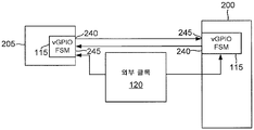
이제 도면들로 돌아가면, 도 1 은 모바일 전화기 또는 다른 통신 디바이스 내에 어플리케이션 프로세서 집적 회로 (100) 및 모뎀 프로세서 집적 회로 (105) 를 포함하는 하이브리드 가상 GPIO 아키텍처 (101) 를 도시한다. 각각의 집적 회로가 전용 송신 라인 및 전용 수신 라인에 커플링하기 때문에, 이에 따라, 어플리케이션 프로세서 집적 회로 (100) 에 대한 송신 라인 (110a) 은 모뎀 프로세서 집적 회로 (105) 에 대한 수신 라인이다. 유사하게, 모뎀 프로세서 집적 회로 (105) 에 대한 송신 라인 (110b) 은 어플리케이션 프로세서 집적 회로 (100) 에 대한 수신 라인이다. 이들 라인들 또는 리드들은 집적 회로들 (100 및 105) 사이의 회로 보드 또는 다른 물리적 상호접속체 상에서 반송된다. 각각의 집적 회로는, 대응하는 송신 라인 (예를 들어, 모뎀 프로세서 집적 회로 (105) 에 대한 라인 (110b)) 에 커플링하기 위한 전용 송신 핀 (112) 을 포함한다. 유사하게, 각각의 집적 회로는, 대응하는 수신 라인 (예를 들어, 모뎀 프로세서 집적 회로 (105) 에 대한 라인 (110a)) 에 커플링하기 위한 전용 수신 핀 (111) 을 포함한다. 각각의 집적 회로에서의 유한 상태 머신 (FSM) (115) 은 32 KHz 슬립 클록과 같은 외부 클록 소스로부터의 외부 클록 신호 (120) 에 관하여 이들 전용 라인들 및 핀들을 사용하여 송신 및 수신을 제어한다.Turning now to the figures, FIG. 1 illustrates a hybrid
어플리케이션 프로세서 집적 회로 (100) 는 프로세서 (101) 를 포함한다. 유사하게, 모뎀 프로세서 집적 회로 (105) 는 프로세서 (102) 를 포함한다. 각각의 프로세서는, GPIO 핀들 (125) 과 종래 방식으로 인터페이싱하는 GPIO 인터페이스 (103) 를 통해 커플링한다. 각각의 하이브리드 GPIO 인터페이스 (103) 를 통해 프로세싱된 신호들의 특정 부분은 종래의 GPIO 신호들 (130) 과 같이 종래의 GPIO 핀들 (125) 상에서 송신 및 수신될 수도 있다. 하지만, GPIO 인터페이스 (103) 를 통해 프로세싱된 신호들의 나머지 부분은 종래의 GPIO 핀들 (125) 을 통해 송신 또는 수신되지 않는다. 대신, 이러한 나머지 신호 부분의 일부는, 전용 송신 핀 및 전용 수신 핀을 사용하여 대응하는 FSM (115) 을 통해 송신 및 수신되는 복수의 가상 GPIO 신호들 (135) 을 포함한다. 각각의 FSM (115) 은 또한, 메시징 신호들 (136) 을 수신 및 송신하는 것에 관하여 대응하는 프로세서와 직접 인터페이싱한다. 메시징 신호들 (136) 은, GPIO 신호들이 아니기 때문에, GPIO 인터페이스들 (103) 을 통해 커플링하지 않는다. 각각의 FSM (115) 은 그 전용 송신 핀 (112) 및 수신 핀 (111) 을 통해 메시징 신호들 (136) 을 송신 및 수신한다. 따라서, 이들 핀들은, 가상 GPIO 신호들 (135) 및 메시징 신호들 (136) 양자 모두를 위해 사용된다는 점에 있어서 "하이브리드" 핀들이다.The application processor integrated
가상 GPIO 신호들 (135) 은, 종래의 GPIO 신호들 (130) 에 대한 경우와 같이 그 자신의 전용 핀들을 각각 갖지 않는다. 이는, 가상 GPIO 신호들 (135) 각각이 그 자신의 핀을 요구하는 종래의 GPIO 실시형태와 비교할 때 하이브리드 가상 GPIO 아키텍처 (101) 가 핀들의 현저한 감소를 달성한다는 점에 있어서 상당히 유리하다. 메시징 신호들 (136) 은, 통상, 또다른 전용 송신 핀 및 또다른 전용 수신 핀도 요구할 것이다. 하지만, 이들 부가적인 핀들은 또한, 본원의 유리한 하이브리드 가상 GPIO 아키텍처에서 제거된다.Virtual GPIO signals 135 each do not have their own dedicated pins as is the case for conventional GPIO signals 130 . This is significantly advantageous in that the hybrid
집적 회로는 단지 하나의 FSM (115) 를 포함할 수도 있거나 또는 다중의 외부 시스템들과 인터페이싱하기 위해 복수의 이들 엘리먼트들을 포함할 수도 있다. 도 2a 는 집적 회로 (200) 가 집적 회로 (205) (그 자신의 FSM (115) 포함) 에서의 원격 프로세서와 통신하기 위한 단일의 FSM (115) 을 포함하는 하이브리드 가상 GPIO 아키텍처를 도시한다. 이에 반하여, 도 2b 에 도시된 집적 회로 (220) 는, 집적 회로들 (225 및 230) 에서의 원격 프로세서들과 각각 통신하기 위한 FSM (115A) 및 FSM (115B) 을 포함한다. 그와 관련하여, 본 명세서에서 논의된 프로세서들과 같은 시스템 온 칩 (SoC) 은 다른 SoC들과의 하이브리드 가상 GPIO 시그널링을 수용하는데 필요한 만큼 많은 FSM들로 구성될 수도 있다. 프로세서가 가질 수도 있는 FSM들의 수와 무관하게, 각각의 FSM 은 도 2a 에 나타낸 바와 같이 그 자신의 전용 송신 핀 (240) 및 수신 핀 (245) 을 사용하여 통신한다.An integrated circuit may include only one
도 1 을 다시 참조하면, 가상 GPIO 신호들 (135) 이 FSM (115) 과 같은 유한 상태 머신을 사용하여 수용되기 때문에, 프로세서들 (101 및 102) 은, 가상 GPIO 신호들 (135) 및 메시징 신호들 (136) 을 여전히 수신할 수 있는 슬립상태 또는 다른 타입의 휴면 상태에 있을 수도 있다. 이러한 방식으로, 가상 GPIO 아키텍처 (101) 는 각각의 GPIO 인터페이스 (103) 에 대한 핀들의 수를 유리하게 절약할 뿐 아니라 저전력이다.Referring back to FIG. 1 , since virtual GPIO signals 135 are accommodated using a finite state machine, such as
본 명세서에서 사용된 바와 같이, "핀" 은, 집적 회로가 회로 보드 상의 리드들 또는 다른 물리적 상호접속체 (예를 들어, 패키지 상호접속체 또는 스루홀 비아 상호접속체) 에 커플링하기 위해 사용하는 패드 또는 실제 핀과 같은 구조물을 커버하기 위한 포괄적인 용어이다. 예를 들어, 각각의 집적 회로가 도 1 에 도시된 바와 같이 16개의 GPIO 핀들 또는 패드들 (125) 을 가지면, 이들 핀들은 8개의 대칭적 GPIO 신호들 (130) (도시 명료화를 위해, 오직 4개의 종래의 GPIO 신호들 #1 내지 #4 만이 도 1 에 도시됨) 또는 16개의 비대칭적 GPIO 신호들 (130) 을 수용하도록 구성될 수 있다. 부가적으로, 각각의 집적 회로는 라인들 (110a 및 110b) 을 사용하여 복수의 n개의 가상 GPIO 신호들 (135) 의 입력/출력 인터페이싱을 수용할 수 있으며, 여기서, n 은 임의의 복수 정수이다. 유사하게, 각각의 집적 회로는 라인들 (110a 및 110b) 을 사용하여 복수의 m개의 메시징 신호들 (136) 의 입력/출력 인터페이싱을 수용할 수 있으며, m 은 양수의 복수 정수이다. 각각의 프로세서 코어에 관하여, GPIO 신호들 (130) 과 가상 GPIO 신호들 (135) 간의 차이가 존재하지 않으며, 이들 신호들 양자는, GPIO 인터페이스 (103) 를 통해 필요에 따라 송신 및 수신되는 단순한 신호들이다. 하지만, 가상 GPIO 신호들 (135) 및 메시징 신호들 (136) 이 종래의 GPIO 신호들 (130) 과 대조적으로 전용 핀들을 갖지 않기 때문에, 가상 GPIO 신호들 (135) 및 메시징 신호들 (136) 은 라인들 (110a 및 110b) 상에서의 송신을 위해 FSM들 (115) 에서 직렬화된다. 수신 시, 각각의 FSM (115) 은 수신된 직렬화된 가상 GPIO 신호들 및 수신된 직렬화된 메시징 신호들을 직렬화해제한다. 따라서, 각각의 FSM (115) 은 가상 GPIO 신호들 (135) 및 메시징 신호들 (136) 에 관하여 직렬화기/직렬화해제기로서 기능한다.As used herein, a “pin” is used by an integrated circuit to couple to leads on a circuit board or other physical interconnect (eg, a package interconnect or through-hole via interconnect). is an umbrella term for covering structures such as pads or actual pins. For example, if each integrated circuit has 16 GPIO pins or
프로세서는 GPIO 신호들 또는 메시징 신호들 중 선택된 신호들에서의 변경들에 응답하여 인터럽트 신호를 수신할 필요가 있을 수도 있다. 가상 GPIO 신호들 (135) 및 메시징 신호들 (136) 에 관하여, 모뎀 전력 관리자 (MPM) (140) 는 인터럽트 구성 레지스터들 (도시 안됨) 을 통해, 프로그래밍됨에 따라, 선택된 GPIO 신호들 또는 메시징 신호들을 모니터링한다. 각각의 가상 GPIO 신호 (135) 는 대응하는 인터럽트 구성 레지스터를 갖는다. 가상 GPIO 신호 (135) 가 그 신호 변경 상태에 응답하여 인터럽트를 생성하도록 요구되면, 대응하는 구성 레지스터는 이에 따라 프로그래밍될 것이다. 유사하게, 가상 GPIO 신호 (135) 또는 메시징 신호 (136) 가 그 신호가 상태를 변경했는지 여부와 무관하게 인터럽트를 생성하지 않는 것이라면, 대응하는 인터럽트 구성 레지스터는 또한 이에 따라 프로그래밍될 것이다. MPM (140) 은 또한 유한 상태 머신을 포함할 수도 있다. 따라서, FSM (115) 과 같이, MPM (140) 은 저전력이고, 그 프로세서가 슬립 모드 또는 일부 다른 휴면 상태에 있는지 여부와 무관하게 활성이다.The processor may need to receive an interrupt signal in response to changes in selected ones of the GPIO signals or messaging signals. With respect to virtual GPIO signals 135 and
가상 GPIO 신호들 (135) 은 송신 세트와 수신 세트로 세분될 수도 있다. 대칭적 시스템에 있어서, 각각의 송신 세트는 동일한 개수를 가질 것이다. 유사하게, 각각의 수신 세트는 동일한 수의 신호들을 가질 것이다. 하지만, 가상 GPIO 아키텍처 (101) 는, 메시징 신호들 (136) 및 가상 GPIO 신호들 (135) 의 송신 세트들이 상이한 사이즈들을 갖고 그리고 메시징 신호들 (136) 및 GPIO 신호들 (135) 의 수신 세트들이 또한 상이한 사이즈들을 갖는 비대칭적 시그널링 실시형태를 용이하게 수용할 수 있다는 점에 있어서 유리하다는 것이 인식될 것이다. 아키텍처 (101) 가 대칭적인지 또는 비대칭적인지와 무관하게, 각각의 FSM (115) 은, 이들 송신 세트들에서의 각각의 신호가 GPIO 인터페이스 (103) 와 FSM (115) 사이에서 그 자신의 리드 상으로 반송된다는 의미에서 GPIO 인터페이스 (103) 로부터 병렬로 가상 GPIO 신호들 (135) 의 송신 세트를 수신한다. 메시징 신호들은 GPIO 신호들이 아니고, 따라서, GPIO 인터페이스 (103) 를 통해 커플링하지 않는다. 그와 관련하여, 각각의 FSM (115) 에 의해 나타낸 바와 같은 하이브리드 인터페이스에는 대응하는 프로세서 (101 또는 102) 에 의해 일부 주변기기 어드레스가 제공될 수도 있다. 각각의 FSM (115) 은 메시징 신호들 (136) 에서의 어드레스 필드 (137) 를 디코딩하도록 구성되어, 소정의 메시징 신호 (136) 는 대응하는 메시징 레지스터 (138) 에 저장될 수도 있다. 이들 메시징 레지스터들 (138) 은 대응하는 프로세서 (101 또는 102) 에 대한 어드레스 공간 내에서 FSM (115) 에 대한 일반 어드레스의 일부 오프셋에 각각 매핑된다. 그 후, MPM (140) 으로부터의 인터럽트에 응답하여, 프로세서 (101 또는 102) 는 메시징 레지스터들 (138) 에 액세스하여 적절한 메시징 신호들 (136) 을 획득할 수 있다. 가상 GPIO 신호들 (135) 과 같이, 메시징 신호들 (136) 도 송신 세트와 수신 세트로 세분될 수도 있다. 아키텍처가 대칭적인지 또는 비대칭적인지와 무관하게, FSM (115) 에 의한 이들 송신 세트들의 결과적인 송신은 단일의 송신 핀 (112) 상으로 발생한다. 하나의 프로세서로부터의 가상 GPIO 신호들 (135) 의 송신 세트는 원격 프로세서에 대한 가상 GPIO 신호들 (135) 의 수신 세트가 된다. 유사하게, 메시징 신호들 (136) 의 송신 세트는 원격 프로세서에 대한 메시징 신호들 (136) 의 수신 세트가 된다. 그 후, 원격 프로세서의 FSM (115) 은 가상 GPIO 신호들 (135) 의 수신 세트를 직렬화해제하여, 이들은 GPIO 인터페이스 (103) 에 병렬로 제시될 수도 있다.The virtual GPIO signals 135 may be subdivided into a transmit set and a receive set. In a symmetric system, each set of transmissions will have the same number. Similarly, each receive set will have the same number of signals. However, the
각각의 FSM (115) 은, 가상 GPIO 신호들 (135) 의 송신 세트에 대한 그리고 메시징 신호들 (136) 에 대한 이전 상태를 저장하는 구성 레지스터들 (도시 안됨) 을 포함한다. 이러한 방식으로, 각각의 FSM (115) 은 GPIO 인터페이스 (103) 로부터 수신된 바와 같은 가상 GPIO 신호들 (135) 의 송신 세트의 현재 상태를 모니터링하고, 현재 상태가 이전 상태에 관하여 변하였으면, 오직 대응하는 송신 세트의 직렬 송신만을 트리거링할 수 있다. 즉, FSM (115) 은, 오직 송신 세트 내의 신호들 중 하나 이상이 구성 레지스터들 (107) 로의 이전 상태의 저장부를 통해 검출된 바와 같이 상태를 변경하였을 경우에만 송신 세트의 직렬 송신을 트리거링할 것이다. 각각의 프로세서는 메시징 신호 레지스터들 (138) 에 대한 어드레스들을 알고, 따라서, 이 어드레스들을 원하는 송신 세트에 기입하고 또한 수신 세트에서 임의의 변경들을 판독할 수 있다. FSM (115) 은 메시징 신호들 (136) 의 송신 세트가 그 이전 송신에 관하여 변경하였는지 여부를 모니터링하고, 이에 따라, 원격 프로세서로의 송신 세트의 송신을 트리거링할 것이다. MSM (140) 은 전술된 바와 같이 수신 세트들이 변경하였는지 여부를 모니터링하고, 변경된 수신 세트가 프로세싱될 수도 있도록 대응하는 프로세서를 인터럽트한다.Each
상기 논의된 바와 같이, 각각의 FSM (115) 은 직렬화기/직렬화해제기로서 작용하여 각각의 송신 세트를 직렬화하고 각각의 수신 세트를 직렬화해제한다. 도 3 은 이들 동작들을 더 잘 예시하기 위한 FSM (115) 의 블록 다이어그램이다. FSM (115) 은 가상 GPIO 신호들 (135) 및 메시징 신호들 (136) 을 멀티플렉싱 모듈 (300) 을 통해 대응하는 프로세서와 교환한다. 멀티플렉싱 모듈은 가상 GPIO 신호들 (135) 에 관하여 가상 GPIO 인터페이스 (103) 를 통해 대응하는 프로세서와 인터페이싱하고, 메시징 신호들 (136) 에 관하여 대응하는 프로세서와 직접 인터페이싱한다. 일 실시형태에 있어서, 각각의 FSM (115) 은 송신 라인 (110a) 상으로의, 가상 GPIO 신호들 (135) 의 송신 세트 또는 메시징 신호들 (136) 의 송신 세트의 송신을, 오직 송신 세트 중 어느 하나에서 변경이 있었던 경우에만 허가할 로직 회로 (301) 를 포함한다. 따라서, 로직 회로 (301) 는 가상 GPIO 신호들 (135) (또는 메시징 신호들 (136)) 의 송신 세트에 대한 현재 상태를 대응하는 구성 레지스터들 (107) 에 저장된 바와 같은 송신 신호들의 이러한 세트에 대한 이전 상태와 비교한다. 예를 들어, 로직 회로 (301) 는 이러한 비교를 수행하기 위한 XOR 게이트 (310) 를 포함할 수도 있다. 멀티플렉싱 모듈 (300) 은 송신 세트를 병렬로, 병렬입력 직렬출력 (PISO) 시프트 레지스터 (315) 로 로딩한다. XOR 게이트 (310) 로부터의 인에이블 신호 (320) 가 (송신 세트에 대한 현재 상태와 이전 상태 간의 변경을 나타내는) 하이 (high) 로 가면, PISO 시프트 레지스터 (315) 는 그 컨텐츠를 외부 클록 (120) 의 사이클들에 응답하여 송신 라인 (110a) 상으로 직렬로 시프트-아웃하도록 인에이블된다.As discussed above, each
FSM (115) 은 또한, 직렬입력 병렬출력 (SIPO) 시프트 레지스터 (325) 를 사용하여 유사한 방식으로 메시징 신호들 (136) 또는 가상 GPIO 신호들 (135) 의 수신 세트를 직렬화해제한다. 메시징 신호들 (136) 및 가상 GPIO 신호들 (135) 의 수신 세트는 원격 프로세서에 의해 생성되고, 원격 프로세서에 의해 수신 라인 (110b) 상으로 송신된다. 가상 GPIO 신호들 (135) (또는 메시징 신호들 (136)) 의 이러한 수신 세트는 외부 클록 (120) 의 사이클들에 응답하여 SIPO 시프트 레지스터 (325) 로 연속적으로 시프트된다. FSM (115) 은, 본 명세서에서 추가로 논의되는 바와 같이, 별도의 시작 비트 및 종료 비트를 갖는 프레임들에 있어서 메시징 신호들 (136) 및 가상 GPIO 신호들 (135) 의 송신 세트를 송신하고 수신 세트를 수신하도록 구성된다.The
일 실시형태에 있어서, FSM (115) 은 GPIO 인터페이스로부터 가상 GPIO 신호들의 송신 세트를 수신하고 가상 GPIO 신호들의 송신 세트를 전용 송신 핀 상으로 원격 프로세서에 직렬로 송신하며, 그리고 메시징 신호 레지스터들로부터 메시징 신호들의 송신 세트를 취출하고 메시징 신호들의 송신 세트를 전용 송신 핀 상으로 원격 프로세서에 직렬로 송신하는 수단을 포함하도록 간주될 수도 있다.In one embodiment, the
프레임들은 미리정의된 사이즈를 갖는다. 일 실시형태에 있어서, 프레임 사이즈는 길이가 특정 수의 비트들인 것으로 헤더에 의해 결정된다. 예시적인 프레임 (400) 이 도 4 에 도시된다. 헤더 (405) 는 2개의 기능 비트들 (fn_0 및 fn_1) 을 포함할 수도 있다. 일 실시형태에 있어서, 기능 비트들 양자 모두가 제로이면, 다음의 비트들은 가상 GPIO 신호들 (135) 이다. fn_0 이 제로이고 fn_1 이 1 과 동일하면, 다음의 비트들은 메시징 신호들 (136) 이다. fn_0 이 1 이고 fn_1 이 0 과 동일하면, 다음의 비트들은 원격 프로세서에 의해 예상될 가상 GPIO 프레임 길이를 나타낸다. 유사하게, 양자 모두의 기능 비트들이 1 이면, 다음의 비트들은 원하는 프레임 길이의 원격 프로세서에 의한 확인응답을 나타낸다. 가상 GPIO 신호들 (135) 의 송신 세트 (또는 메시징 신호들 (136) 의 송신 세트) 가 이러한 고정된 프레임 사이즈 미만이면, 각각의 프레임 내의 미사용 비트들은 무정의 (don't care) 값들일 수도 있다. 대안적으로, 각각의 FSM (115) 은, 소정의 어플리케이션에 대해 필요한 비트들의 수에 의존하여, 송신된 프레임들의 사이즈를 변경하도록 구성될 수도 있다. 2개의 기능 비트들을 사용한 코딩의 앞선 논의는 단지 일 예일 뿐이며 프레임이 가상 GPIO 신호들 (135), 메시징 신호들 (136), 가상 GPIO 프레임 길이의 식별, 가상 GPIO 프레임 길이의 확인응답, 메시징 신호 프레임 길이의 식별, 또는 메시징 길이 프레임 길이의 확인응답을 반송하고 있는지 여부를 식별하기 위하여 다른 헤더들 및 코딩 프로토콜들이 사용될 수도 있음이 인식될 것이다. 일 실시형태에 있어서, 프레임 (400) 은 또한, 하기에서 더 논의되는 바와 같이 프로그래밍 및 확인응답 프레임들과 연관되는 타입 비트 (type_bit) 를 포함할 수도 있다. 예를 들어, 일 실시형태에 있어서, 타입 비트는 가상 GPIO 프레임을 식별하기 위하여 하이이고 메시징 신호 프레임을 식별하기 위하여 로우일 수도 있다.Frames have a predefined size. In one embodiment, the frame size is determined by the header to be a certain number of bits in length. An
메시징 신호들 (136) 또는 가상 GPIO 신호 (135) 의 송신 세트를 전송하기 위해 요구된 프레임들의 수는 특정 송신 세트에서의 신호들의 수 및 프레임 사이즈에 의존한다. 예를 들어, 프레임 사이즈가 8 비트이고 송신 세트에 10개의 가상 GPIO 신호들 (135) 이 존재한다고 가정한다. 따라서, 그 송신 세트를 전송하기 위하여, 8비트 프레임들을 사용하는 것은 2개의 프레임들을 요구할 것이다.The number of frames required to transmit a transmission set of messaging signals 136 or
메시징 신호들 (136) 또는 가상 GPIO 신호들 (135) 의 수신 세트에 대한 완전한 프레임의 수신을 검출하기 위해, FSM (115) 은, 프레임에 대한 시작 비트의 수신 이후 외부 클록 (120) 에 대한 사이클들의 필요한 수를 카운트하는 도 3 에 도시된 바와 같은 로직 회로 (350) 를 포함할 수도 있다. 예를 들어, 수신 세트는, 외부 클록 (120) 의 10개 사이클들에 응답하여 수신되는 10개의 가상 GPIO 신호들 (135) 을 포함한다고 가정한다. 시작 비트의 검출 및 외부 클록 (120) 의 다른 10개 사이클들의 대기 이후, 로직 회로 (350) 는 종료 비트의 수신을 예상할 것이다. 이에 따라 종료 비트가 검출되면, 로직 회로 (350) 는, 완전한 프레임으로서 SIPO 시프트 레지스터 (325) 로 시프트되었던 가상 GPIO 신호들 (135) 의 수신 신호를 병렬로 수신하기 위해 출력 래치 (351) 를 스트로브할 수도 있다. 그 후, 가상 GPIO 신호들의 래치된 수신 세트는 멀티플렉싱 모듈 (300) 을 통해 GPIO 인터페이스 (103) 에 제시될 수도 있다. 메시징 신호들 (136) 의 수신된 세트의 래칭이 유사하게 발생하더라도, 메시징 신호들의 수신된 세트는 GPIO 인터페이스 (103) 를 통해 라우팅되는 대신 메시징 신호 레지스터들 (138) 로 로딩된다.To detect receipt of a complete frame for the received set of messaging signals 136 or virtual GPIO signals 135 ,
PISO 시프트 레지스터 (315) 를 다시 참조하면, 이 레지스터는 메시징 신호들 및 가상 GPIO 신호들의 송신 세트를 시작 및 종료 비트들로 프레이밍하도록 구성됨이 인식될 것이다. 따라서, 가상 GPIO 신호들의 송신 세트는, 시작 및 종료 비트들에 의해 구분되는 프레임 (400) 에서 송신된다. 송신 프로세서에 대한 송신 세트가 원격 프로세서에 대한 수신 세트가 되기 때문에, 이에 따라, 수신 세트가 또한 프레이밍된다. 이러한 프레이밍은, 각각의 프로세서가 임의의 부가적인 전용 핀들을 필요로 하는 일없이 원격 프로세서의 강건성을 그후 모니터링할 수 있다는 점에 있어서 유리하다. 예를 들어, 각각의 FSM (115) 은 디폴트 상태 (가상 GPIO 신호들의 송신 세트에 대한 현재 상태 대 이전 상태의 변경 없음) 동안 공급 전압으로 그 전용 송신 핀 (112) 을 약하게 풀링 (따라서, 송신 라인 (110a) 을 약하게 풀링) 하도록 구성될 수도 있다. 시작 비트는, FSM (115) 이 시작 비트의 송신을 위해 송신 라인 (110a) 을 접지하도록 하는 그러한 실시형태에 대해 논리 제로일 것이다. 이러한 방식으로, 각각의 FSM (115) 은, 수신 라인 (110b) 이 접지를 향해 풀링되었음을 검출함으로써 시작 비트의 수신을 용이하게 검출할 수도 있다. 일 실시형태에 있어서, 시작 및 중지 비트들은 서로 논리 보수들이다. 따라서, 시작 비트가 로직 제로이면, 중지 비트는 로직 하이 값일 것이다. 그 후, 프레임의 페이로드는 타입 비트로부터, 프레임 종료를 구분하는 중지 비트 (410) 로 확장할 수도 있다.Referring back to the
프로세서가 실패하여 그 송신 라인 (110a) 을 접지로 부적절하게 풀링할 가능성이 존재한다. 따라서, 원격 프로세서는 이것을 시작 비트로서 검출할 것이고, 로직 회로 (350) 는 이에 따라 프레임의 종료를 향해 카운트하기 시작할 것이다. 하지만, 종료 비트가 로직 1 이면, 각각의 FSM (115) 은 송신 라인 (110a) 을 공급 전압으로 차징 (charge) 하여 프레임 송신의 종료를 시그널링한다. 프로세서가 실패하여 원격 FSM (115) 이 시작 비트로 간주되는 것을 검출하였으면, 로직 회로 (350) 는 종료 비트를 검출하지 못할 것이고, 이에 따라, 그 프로세서에게 원격 프로세서의 실패를 통지할 것이다.There is a possibility that the processor will fail and improperly pull its transmit
수신을 위한 충분한 셋업 시간을 허용하기 위하여, 프레임 (400) 의 송신은 제 1 클록 에지에 관하여 발생할 것이고 수신은 나머지 클록 에지에 관하여 발생할 것이다. 예를 들어, PISO 시프트 레지스터 (315) 에서의 비트들은 외부 클록 (120) 에 대한 하강 에지들 또는 네거티브 에지들에 응답하여 송신 라인 (110a) 상에서의 송신을 위해 시프트-아웃될 수도 있다. 반면, 수신 라인 (110b) 상에서의 수신된 비트들은 클록 (120) 의 상승 에지들 또는 포지티브 에지들에 응답하여 SIPO 시프트 레지스터 (325) 로 시프트될 수도 있다.To allow sufficient setup time for reception, transmission of
하나의 프로세서가 원격 프로세서에서 비활성 상태를 검출하기 위해, 각각의 FSM (115) 은 그 송신 라인을 (송신할 어떠한 프레임들도 존재하지 않는) 디폴트 상태에서 하이로 약하게 풀링하도록 구성될 수도 있다. 전술된 바와 같이, 시작 및 중지 비트들은 반대 논리 상태들을 갖는다. 따라서, 도 4 의 프레임 (400) 에 대한 시작 비트 (406) 는 송신 라인 (110a) 이 그 송신에 대해 로우로 풀링되도록 로직 제로 (접지) 일 수도 있지만, 중지 비트 (410) 는 송신 라인 (110a) 이 그 송신에 대해 전력 공급 전압으로 하이로 풀링되도록 바이너리 1 값일 수도 있다. 도 3 을 다시 참조하면, 로직 회로 (350) 는 외부 클록 (120) 상의 상승 에지들에 관하여 수신 라인 (110b) 을 모니터링하도록 구성된다. 비-프레임 송신의 디폴트 로직 상태는, 전술된 바와 같이 그 약한 풀링-업때문에 하이로 단순히 남겨진 수신 라인 (110b) 에 의해 표시된다. 로직 회로 (350) 가 수신 라인 (110b) 이 (시작 비트 (405) 의 제로 값을 나타내는) 로우로 풀링되었음을 외부 클록 (120) 에 대한 상승 에지들 중 하나에서 검출하면, 로직 회로 (350) 는 프레임 (400) 의 미리정의된 사이즈에 따라 충분한 수의 클록 사이클들 동안 대기하여, 그 후, 중지 비트 (410) 의 로직 하이 값을 검출한다. 중지 비트 (410) 의 수신은, 완전한 프레임 (400) 이 SIPO 시프트 레지스터 (325) 로 완전히 시프트되었음을 로직 회로 (350) 에게 나타낸다. 그 시점에서, 로직 회로 (350) 는 SIPO 시프트 레지스터 (325) 를 스트로브하여 수신된 프레임이 래치 (351) 를 통해 멀티플렉싱 모듈 (300) 에 병렬로 제공된다. 그 후, 가상 GPIO 신호들 (또는 메시징 신호들 (136)) 의 수신 세트는, 이에 따라, GPIO 인터페이스 (103) 를 통해 프로세서 코어에 제공될 수도 있다.In order for one processor to detect inactivity at a remote processor, each
32 KHz 슬립 클록과 같은 상대적으로 느린 외부 클록 (120) 은 IPC 의 시그널링 요건들에 대해 충분하다. 예를 들어, 가상 GPIO 신호들 (135) 및 메시징 신호들 (136) 의 송신을 위한 최소 셋업 및 유지 요건들은 각각 2 나노초이고 그리고 FSM (115) 에서의 외부 클록 (120) 의 수신을 위한 최대 예상 리드 또는 래그는 6 나노초라고 가정한다. 외부 클록 (120) 에 대한 결과적인 최대 주파수는 62 MHz 일 것임이 용이하게 나타내어질 수 있다. 따라서, 예컨대 슬립 클록으로부터의 32 KHz 주파수는 그러한 실시형태에 대해 매우 큰 안전 마진들을 제공할 것이다. 이제, 아키텍처 (101) 에 대한 예시적인 동작 방법이 요약될 것이다.A relatively slow
아키텍처 (101) 에 대한 동작 방법은 도 5 의 플로우차트에서 요약된다. 그 방법은, 단계 500 에 있어서, GPIO 인터페이스에서의 GPIO 신호들의 세트를 제 1 프로세서로부터 수신하는 것으로 시작한다. 단계 505 는, GPIO 인터페이스로부터, GPIO 신호들의 세트의 일부를 GPIO 핀들을 통해 원격 프로세서에 송신하는 것을 포함한다. 단계 510 은, GPIO 인터페이스로부터, GPIO 신호들의 세트의 나머지 부분을 가상 GPIO 신호들로서 전용 송신 핀 신호들 상으로 원격 프로세서에 직렬로 송신하는 것을 포함한다. 마지막으로, 그 방법은, 제 1 프로세서에 의해 기입된 메시징 신호 레지스터들로부터 메시징 신호들을 취출하고, 취출된 메시징 신호들을 전용 송신 핀 상으로 원격 프로세서에 직렬로 송신하는 동작 515 를 포함한다.The method of operation for
개시된 가상 하이브리드 GPIO 아키텍처의 이점들: 즉, 오직 2개의 핀들만이 필요하고 게다가 임의의 수의 가상 GPIO 신호들 (135) 및 메시징 신호들 (136) 이 유한 상태 머신들을 통해 직렬화 및 직렬화해제될 수 있다는 이점을 고려한다. 유일한 제한은 임의의 예상된 양의 클록 래그 또는 리드 및 외부 클록 (120) 에 관한 가상 GPIO 신호들에 대한 타이밍 요건들이다. 더욱이, 하나의 프로세서의 강건성을 대향 프로세서에 투명하게 하기 위해 어떠한 다른 핀들도 필요하지 않다.Advantages of the disclosed virtual hybrid GPIO architecture: that is, only two pins are needed and furthermore any number of virtual GPIO signals 135 and
프레임 (400) 은 또한, 단지 2개의 기능 비트들만큼 작은 오버헤드만으로, 다양한 메시징 신호들 (136) 및 가상 GPIO 신호들 (135) 이 전용 송신 핀 (112) 상으로 송신될 수도 있다는 점에 있어서 상당히 유리하다. 가상 GPIO 프레임 길이를 설정하기 위한 (및 메시징 신호 프레임 길이를 설정하기 위한) 예시적인 프로그래밍 프레임들이 도 6 에 도시된다. 프로그래밍 프레임 (600) 은 가상 GPIO 프레임 길이를 설정한다. 유사하게, 프로그래밍 프레임 (605) 은 메시징 신호 프레임 길이를 설정한다. 프레임 길이 (따라서, 각각의 프로그래밍 프레임의 길이) 를 정의하기 위해 사용된 비트들의 수는 미리정의된다. 따라서, FSM (115) 은, 프로그래밍 길이가 설정되어 있음 (예컨대, 전술된 바와 같이 fn_0 은 1 과 동일하고 fn_1 은 0 과 동일) 을 표시하는 헤더를 알면, 프레임 바디로부터 프레임 길이를 판독할 것이다. 그와 관련하여, FSM (115) 은 가상 GPIO 프레임 또는 메시징 프레임의 길이가 프로그래밍되어 있는지 여부를 알 필요가 있다. 따라서, 프로그래밍 프레임들 (600 및 605) 에 대한 각각의 헤더 (405) 다음에는 프레임 타입 비트 (610) 가 이어진다. 예를 들어, 1 과 동일한 프레임 타입 비트 (610) 는 가상 GPIO 프레임 길이가 프로그래밍되어 있음을 나타낼 수도 있지만, 제로와 동일한 프레임 타입 비트 (610) 는 메시징 신호 프레임 길이가 프로그래밍되어 있음을 나타낼 수도 있다. 일 실시형태에 있어서, 각각의 프로그래밍 프레임 (600 및 605) 은 비트-0 으로부터 비트-4 까지에 이르는 5개 프로그래밍 비트들을 갖는다. 각각의 비트는 그 명칭에 의해 식별된 바와 같이 2 의 거듭제곱에 대한 계수이다. 즉, 비트-0 은 20 을 승산하기 위한 계수이고, 비트-1 은 21 을 승산하기 위한 계수이고, 비트-2 는 22 을 승산하기 위한 계수이고, 비트-3 은 23 을 승산하기 위한 계수이며, 비트-4 는 24 을 승산하기 위한 계수이다. 따라서, 5개 프로그래밍 비트들은 제로로부터 31 까지의 프레임 길이를 프로그래밍할 수 있다. 부가적인 프로그래밍 비트는 63 까지의 프레임 길이의 프로그래밍을 인에이블하는 등등일 것이다.The
원격 FSM (115) 은, 프레임 (600 또는 605) 과 같은 프로그래밍 프레임을 수신할 경우, 정의된 프레임 길이를 확인응답 프레임을 사용하여 확인응답하도록 진행할 수도 있다. 예시적인 확인응답 프레임들이 도 7 에 도시된다. 프레임 (700) 은 가상 GPIO 확인응답 프레임이지만 프레임 (705) 은 메시징 신호 확인응답 프레임이다. 각각의 프레임 (700 및 705) 은, 기능 비트들이 프레임을 확인응답 프레임으로서 식별하는 헤더 (405) 를 포함한다. 일 실시형태에 있어서, 양자의 기능 비트들이 로직 1 인 헤더 (405) 는 확인응답 프레임을 식별한다. 헤더 (405) 이후의 프레임 타입 비트 (710) 는 확인응답 프레임 타입을 식별한다. 일 실시형태에 있어서, 가상 GPIO 확인응답 프레임 (700) 은 로직 1 과 동일한 프레임 타입 비트 (710) 에 의해 식별된다. 반면, 메시징 신호 확인응답 프레임 (705) 은 로직 제로와 동일한 프레임 타입 비트 (710) 에 의해 식별될 수도 있다. 프레임 타입 비트 (710) 이후의 프로그래밍 비트들은 대응하는 프레임들 (600 또는 605) 에서의 프로그래밍 비트들과 동일하다.When the
따라서, 일단 프레임 길이들이 프로그래밍되면, 가상 GPIO 신호들 (136) 의 프레임 (800) 또는 메시징 신호들의 프레임 (805) 은 도 8 에 도시된 바와 같이 송신될 수도 있다. 도 1 을 다시 참조하면, n개의 가상 GPIO 신호들 (135) 및 m개의 메시징 신호들 (136) 이 존재함을 유의한다. 따라서, 각각의 프레임 (800) 은 단지 하나의 GPIO 포트 (n개의 GPIO 신호들 (135) 중 하나) 에 전용될 수 있거나 또는 n개의 GPIO 신호들 (135) 로부터 각각 일 비트를 포함할 수 있다. 즉, 다양한 포트들에 따라 GPIO 워드들을 직렬로 송신할 수 있거나 또는 병렬로 송신될 수 있다. 동일한 직렬/병렬 고려사항이 메시징 신호들에 적용된다. 각각의 프레임 (800 및 805) 이 다중의 포트들 또는 단지 하나의 포트를 반송하고 있는지 여부와 무관하게, 헤더 (405) 는 프레임이 가상 GPIO 프레임이지 또는 메시징 신호 프레임인지를 식별한다.Accordingly, once the frame lengths are programmed, the
가상 GPIO 신호들 (135) 및 메시징 신호들 (136) 을 송신하기 위해 별도의 프레임들을 사용하는 것보다는, 이들 신호들은, 각각의 프레임이 가상 GPIO 신호들 (135) 및 메시징 신호들 (136) 양자 모두를 포함하는 하이브리드 가상 GPIO 아키텍처를 위한 대안적인 실시형태에 있어서, 결합될 수도 있다. 예를 들어, 도 9 는 헤더 (405) 뿐 아니라 확장된 헤더 (905) 를 포함하는 예시적인 하이브리드 프레임 (900) 을 도시한다. 확장된 헤더 (905) 는, 확장된 헤더 (905) 이후 및 중지 비트 (410) 이전 메시징 신호 비트들 및 가상 GPIO 비트들의 비트 포지션을 표시한다. 레이턴시 요건들에 의존하여, 메시징 비트들 (910) 또는 가상 GPIO 비트들 (915) 중 어느 하나가 프레임 바디에 먼저 있을 수도 있다. 일부 실시형태들에 있어서, 확장된 헤더 (905) 는 CRC 비트들과 같은 에러 정정 비트들을 포함할 수도 있다. 확장된 헤더 (912) 는 오직 가상 GPIO 비트들 (915) 만 또는 오직 메시징 비트들 (910) 만의 포지션 및 길이만을 식별할 필요가 있는데, 왜냐하면 이에 따라 나머지 비트들은 디폴트로 나머지 비트 카테고리에 속하도록 알려지기 때문임을 유의한다.Rather than using separate frames to transmit the virtual GPIO signals 135 and the messaging signals 136 , these signals indicate that each frame is both the virtual GPIO signals 135 and the messaging signals 136 . In an alternative embodiment for an all-inclusive hybrid virtual GPIO architecture, they may be combined. For example, FIG. 9 shows an
상기 논의된 바와 같이 공통 외부 클록 (120) 의 사용은 구현하기에 편리하게 단순하지만, 각각의 FSM (115) 이 공통 클록 (120) 을 수신하기 위한 클록 핀과 연관될 것을 요구한다. 이러한 부가적인 핀 요구를 회피하기 위하여, 외부 클록 (120) 은 미국 가출원 제61/907,974호에서 논의된 바와 같이 제거될 수도 있으며, 이 가출원의 내용은 본 명세서에 참조로 통합된다. 따라서, 도 1 을 다시 참조하면, 아키텍처 (101) 는 외부 클록 (102) 및 그 대응하는 핀들을 제거함으로써 수정될 것이다. 공통 클록 (120) 을 수신하기 위한 각각의 집적 회로에 핀을 보유하기 위한 어떠한 필요성도 제거하기 위해, 신호들의 송신 세트의 송신은 송신 집적 회로 및 수신 집적 회로에 관하여 비동기식이다. 이러한 유리한 비동기식 송신 및 수신을 인에이블하기 위하여, 각각의 FSM (115) 은 링 오실레이터와 같은 오실레이터를 포함하거나 그 오실레이터와 연관시킬 수도 있다. 송신 FSM 펄스폭은, 오실레이터로부터의 오실레이션들을 카운트함으로써 송신 세트에서의 각각의 비트에 응답하여 전용 송신 핀 상으로의 송신된 신호를 변조한다. 그 후, 송신 세트에서의 비트들은 데이터의 프레임들에서 송신되고, 프레임에서의 각각의 비트는 송신 세트에서의 대응하는 비트의 펄스폭 변조된 버전이다. 데이터의 송신된 프레임에서의 각각의 비트는, 펄스폭 변조에 관하여 사용되는 특정 비트 주기를 갖는다. 예를 들어, 송신 비트가 바이너리 제로와 같은 하나의 바이너리 상태를 가지면, FSM 은, 비트 주기의 다수 비율이 만료하도록 오실레이션들의 제 1 수를 카운트할 수도 있다. 오실레이션들의 제 1 수를 카운트할 시, FSM 은 제 1 바이너리 전압으로, 예컨대 전력 공급 전압 (VDD) 으로 전용 송신 핀을 펄싱한다. 카운트의 시작부에서, 전용 송신 핀은 접지와 같은 반대의 제 2 바이너리 전압 상태에서 펄싱된다.The use of a common
반면, 송신 비트가 바이너리 1 과 같은 반대의 바이너리 상태를 가지면, FSM 은 접지와 같은 제 2 바이너리 전압으로 송신 비트를 시작하고, 비트 주기의 소수 비율이 만료하도록 오실레이션들의 제 2 수를 카운트하도록 진행한다. 오실레이션들의 제 2 수를 카운트할 시, FSM 은 제 1 바이너리 전압으로 전용 송신 핀을 펄싱한다. 이러한 방식으로, 전용 송신 핀에 커플링된 송신 라인의 전압은 가변 펄스폭에 따라 제 1 바이너리 전압으로 펄싱된다. 현재 송신 비트가 제 1 바이너리 값을 가지면, 송신 라인은 제 1 펄스폭에 따라 제 1 바이너리 전압으로 펄싱된다. 반면, 현재 송신 비트가 반대의 제 2 바이너리 값을 가지면, 송신 라인은 제 2 펄스폭에 따라 제 1 바이너리 전압으로 펄싱된다.On the other hand, if the transmit bit has an opposite binary state, such as binary one, the FSM starts the transmit bit with a second binary voltage, such as ground, and proceeds to count the second number of oscillations such that the fractional ratio of the bit period expires. do. Upon counting the second number of oscillations, the FSM pulses the dedicated transmit pin with the first binary voltage. In this manner, the voltage of the transmit line coupled to the dedicated transmit pin is pulsed with a first binary voltage according to the variable pulse width. If the current transmit bit has a first binary value, the transmit line is pulsed with a first binary voltage according to the first pulse width. On the other hand, if the current transmission bit has an opposite second binary value, the transmission line is pulsed with the first binary voltage according to the second pulse width.
원격 프로세서로부터의 데이터의 송신된 프레임의 FSM 에서의 그 전용 수신 핀 상으로의 수신은 유사한 방식으로 복조된다. (수신 프로세서에 대한 수신 라인인) 각각의 송신 라인의 디폴트 상태 (또는 유휴 모드) 가 전력 공급 전압 (VDD) 으로 차징되는 것이 편리하다. 이는, 하기에서 더 논의되는 바와 같이, 원격 프로세서의 강건성을 수신 프로세서에 투명하게 한다. 그 후, 그러한 실시형태들에 있어서의 제 2 바이너리 전압은 접지일 것이다. 그 후, 수신 FSM 은, 전용 수신 핀이 디스차징된 때를 검출함으로써 수신된 비트의 시작을 인식할 것이다. 그 후, 수신 FSM 은 그 오실레이터로부터의 오실레이션을 카운트하기 시작할 수도 있다. 그 후, 2개의 카운트들이 생성될 것이다: 즉, 전용 수신 핀이 제 1 바이너리 전압으로 차징되는 비트 비율 동안 얼마나 많은 오실레이션들이 발생하는지의 제 1 수신 카운트, 및 전용 수신 핀이 제 2 바이너리 전압으로 차징되는 비트 비율 동안 얼마나 많은 오실레이션들이 발생하는지의 제 2 수신 카운트. 2개의 수신 카운트들을 비교함으로써, 수신 FSM 은 수신된 비트에 제 1 펄스폭이 적용되었는지 또는 제 2 펄스폭이 적용되었는지를 결정할 수도 있다. 이에 따라, 데이터의 수신된 프레임은, 어떠한 공통 클록도 송신 라인들 상으로의 데이터의 프레임들의 송신을 조정하도록 요구되지 않도록 복조된다. 외부 클록을 사용하는 그러한 FSM 을 FSM (115) 으로부터 구별하기 위하여, 다음의 FSM 이 내부 클록 FSM 으로서 표기될 것이다.Reception of the transmitted frame of data from the remote processor on its dedicated receive pin at the FSM is demodulated in a similar manner. It is convenient for the default state (or idle mode) of each transmit line (which is the receive line to the receive processor) to be charged to the power supply voltage VDD. This makes the remote processor's robustness transparent to the receiving processor, as discussed further below. The second binary voltage in such embodiments will then be ground. The receive FSM will then recognize the start of the received bit by detecting when the dedicated receive pin has been discharged. The receiving FSM may then start counting oscillations from that oscillator. Thereafter, two counts will be generated: a first receive count of how many oscillations occur during the bit rate at which the dedicated receive pin is charged to the first binary voltage, and a first receive count when the dedicated receive pin is charged to the second binary voltage. A second receive count of how many oscillations occur during the charged bit rate. By comparing the two receive counts, the receive FSM may determine whether a first pulse width or a second pulse width has been applied to the received bit. Accordingly, the received frame of data is demodulated such that no common clock is required to coordinate the transmission of the frames of data on the transmission lines. To distinguish such FSMs using an external clock from
도 10 은, 그 송신 및 수신 동작들을 더 잘 예시하기 위한 내부 클록 FSM (1015) 의 블록 다이어그램이다. FSM (1015) 은 가상 GPIO 신호들 (135) 의 송신 세트를, (도 1 에 도시된) 그 GPIO 인터페이스 (103) 로부터 멀티플렉싱 모듈 (300) 을 통해 수신한다. 대안적으로, 멀티플렉싱 모듈 (300) 은 FSM (115) 에 관하여 전술된 바와 같이 메시징 신호들 (136) 의 송신 세트를 수신할 수도 있다. FSM (1015) 은 송신 라인 (110a) 상으로의 펄스폭 변조된 신호들로서의 신호의 송신 세트의 직렬 송신을, 송신 세트의 이전 상태와 비교할 때 송신 세트에서 변경이 있었던 경우에 허가할 로직 회로 (301) 를 포함한다. 이러한 방식으로, 이전 송신과 비교할 때 상태를 변경하지 않은 송신 세트의 불필요한 재송신은 존재하지 않는다. 따라서, 로직 회로 (301) 는 가상 GPIO 신호들의 현재 송신 세트를 래치 또는 구성 레지스터 (107) 에 저장된 이전 송신 세트와 비교한다. 비교를 수행하기 위하여, 로직 회로 (301) 는, 현재 송신 세트를 구성 레지스터들 (107) 에 저장된 이전 송신 세트 (이 이전 송신 세트는 도 2 에 도시된 바와 같이 "마지막 GPIO 스테이터스" 로서 지정될 수도 있음) 와 XOR하는 XOR 게이트 (310) 를 포함할 수도 있다. 멀티플렉싱 모듈 (300) 은 현재 송신 세트를 병렬로, 병렬입력 직렬출력 (PISO) 시프트 레지스터 (315) 로 로딩한다. XOR 게이트 (310) 로부터의 인에이블 신호 (320) 가 (현재 송신 세트와 레지스터들 (107) 에 저장된 송신 세트 간의 변경을 나타내는) 하이로 가면, PISO 시프트 레지스터 (315) 는 그 컨텐츠를 시프트 신호 (120) 에 응답하여 송신 라인 (110a) 상으로 직렬로 시프트-아웃하도록 인에이블된다.10 is a block diagram of an internal clock FSM 1015 to better illustrate its transmit and receive operations. The FSM 1015 receives a transmit set of virtual GPIO signals 135 from its GPIO interface 103 (shown in FIG. 1 ) via the
신호들의 각각의 송신 세트는, PISO 시프트 레지스터 (315) 에 저장되는 데이터의 프레임을 포함한다. FSM (1015) 은, PISO 시프트 레지스터 (315) 로부터 송신 라인 (110a) 상에서 원격 프로세서에 구동된 펄스폭 변조된 출력 신호로 시프트-아웃된 비트들의 송신 세트를 펄스폭 변조하는 펄스폭 변조기 (355) 를 포함한다. 이러한 변조는, 송신 링 오실레이터 (RO) (361) 로부터의 송신 링 오실레이터 출력 신호 (360) 의 카운트들과 같은 오실레이터로부터의 오실레이션 사이클들의 카운트들에 응답한다. 변조기 (355) 및 송신 링 오실레이터 (361) 는 XOR 게이트 (310) 로부터의 인에이블 신호 (320) 의 어써션 (assertion) 에 의해 트리거링될 수도 있다. 이러한 트리거링에 응답하여, 변조기 (355) 는 시프트 신호 (120) 를 스트로브하여, PISO 시프트 레지스터 (315) 가 신호들의 송신 세트의 초기 비트를 변조기 (355) 로 시프트한다.Each transmit set of signals includes a frame of data that is stored in the
변조기 (355) 는, 링 오실레이터 출력 신호 (360) 에서의 사이클들을 카운트하는 적어도 하나의 카운터 (예를 들어, 하기에서 더 설명되는 도 11 에 도시된 카운터들 (1105 및 1110)) 를 포함한다. 펄스폭 변조로부터의 원하는 펄스폭에 의존하여, 카운터는 제 1 카운트로 또는 제 1 카운트보다 큰 제 2 카운트로 카운트한다. 제 1 카운트 및 제 2 카운트 중 적절한 하나의 카운트를 충족시키기 위해 충분한 수의 사이클들을 카운트한 이후, 카운터는 시프트 신호 (120) 를 재-스트로브하여 PISO 시프트 레지스터 (315) 에 저장된 데이터의 프레임으로부터의 후속 비트가 변조기 (355) 로 시프트된다. 이러한 방식으로, PISO 시프트 레지스터 (315) 에 저장된 데이터의 프레임에 대한 신호들의 송신 세트는 변조기 (355) 로 한번에 일 비트 시프트된다. PISO 시프트 레지스터 (315) 의 시프트-아웃된 각각의 비트의 바이너리 값에 의존하여, 펄스폭 변조기 (355) 는 송신 라인 (110a) 상으로 송신된 대응하는 펄스를 펄스폭 변조한다. 그와 관련하여, 각각의 프로세서는 디폴트 상태 (데이터 송신 없음) 동안 그 송신 라인 (110a) 을 하이로 전력 공급 전압 (VDD) 으로 약하게 차징하도록 구성될 수도 있다. 그러한 실시형태에 있어서, 비트 시간 주기 동안의 펄스 송신은, 데이터의 프레임에 대해 도 11 의 타이밍 다이어그램에서 도시된 바와 같이, 송신 라인 (110a) 을 접지 (VSS) 로 디스차징하는 것으로 시작한다. 각각의 펄스폭 변조된 비트 송신은, 비트 시간 주기의 25% 와 같은 비트 주기의 일부 초기 디스차지 비율만큼의 송신 라인 (110a) 의 접지로의 디스차징으로 시작한다. 비트 값에 의존하여, 변조기 (355) 는 비트 주기의 대부분 (예를 들어, 75%) 동안 송신 라인 (110a) 의 디스차지를 유지하거나, 또는 비트 주기의 초기 디스차지 비율의 만료 직후 송신 라인 (110a) 를 다시 VDD 로 차징한다. 즉, 일 바이너리 값은 비트 주기에 있어서 고 전압 (VDD) 의 상대적으로 좁은 펄스로 변조될 수도 있지만, 바이너리 값의 보수는 비트 주기에 있어서 고 전압 (VDD) 의 상대적으로 넓은 펄스로 변조될 수도 있다.The
도 11 에 도시된 예시적인 데이터 프레임의 초기 비트는 바이너리 제로이다. 일 실시형태에 있어서, 바이너리 제로는, 송신 라인 (110a) 이 비트 주기의 75% 동안 접지로 유지되는 제 1 펄스폭으로 변조될 수도 있다. 비트 주기의 그러한 다수 비율은, 제 2 카운트로 카운트하는 다수 비율 카운터 (1110) 에 대응한다. 송신될 비트가 바이너리 제로이면, 이에 따라, 펄스폭 변조기 (355) 는, 제 2 카운트가 충족될 때까지 송신 라인 (110a) 을 디스차징으로 유지할 것이다. 제 2 카운트가 도달될 경우, 펄스폭 변조기 (355) 는 비트 주기의 나머지 동안 송신 라인 (110a) 을 전력 공급 전압 (VDD) 으로 펄싱할 것이다. 그 후, 이러한 펄스 지속기간은 제 1 카운트로 카운트하는 소수 비율 카운터 (1105) 에 대응할 것이며, 이는 비트 주기의 단지 25% 이다. 그 후, 그러한 비트에 대한 송신 라인 (110a) 상으로 송신된 결과적인 전압 펄스는 비트 주기의 단지 25% 의 펄스폭을 가질 것이다.The initial bits of the exemplary data frame shown in FIG. 11 are binary zeros. In one embodiment, the binary zero may be modulated with a first pulse width in which the
반면, 바이너리 1 은, 송신 라인 (110a) 이 오직 비트 주기의 첫번째 25% 와 같은 소수 디스차지 비율 동안에만 접지되는 제 2 펄스폭으로 변조될 수도 있다. 그 후, 송신 라인 (110a) 은 제 1 카운트가 충족될 때까지 디스차징될 것이다. 일단 제 1 카운트가 충족되면, 펄스폭 변조기 (355) 는, 다수 비율 카운터 (410) 를 제로로 리셋하고 그리고 제 2 카운트를 충족할 때까지 카운트함으로써 결정되는 바와 같은 비트 주기의 나머지 동안 송신 라인 (110a) 을 하이로 전력 공급 전압 (VDD) 으로 펄싱할 것이다. 그 후, 송신 라인 (110a) 에 대한 전압이 전력 공급 전압 (VDD) 으로 차징되는 제 2 펄스폭은 비트 주기의 75% 를 포함한다. 하지만, 상이한 펄스폭들이 원하는 바이너리 값들을 나타내기 위하여 대안적인 실시형태에서 사용될 수도 있음이 인식될 것이다.
일 실시형태에 있어서, 변조기 (355) 는 로직 회로 (1100) 를 포함할 수도 있다. 비트 값에 의존하여, 로직 회로 (1100) 는 소수 비율 카운터 (1105) 또는 다수 비율 카운터 (1110) 중 어느 하나를 트리거링하여 카운팅을 시작한다. 하지만, 원하는 펄스폭 변조에 의존하여 제 1 카운트 또는 제 2 카운트 중 어느 하나에서 카운트하는 단일의 카운터가 사용될 수도 있음이 인식될 것이다. 로직 회로 (1100) 에 의한 트리거링 시, 소수 비율 카운터 (1105) 또는 다수 비율 카운터 (1110) 는 송신 링 오실레이터 (RO) (361) 로부터의 사이클들을 카운트한다. 예를 들어, 소수 비율 카운터 (1105) 는, 제 1 카운트가 충족됨을 나타내도록 출력 신호를 어써트하는 비트 시간 주기의 25% 에 대응하는 충분한 수의 사이클들을 카운트하도록 구성될 수도 있다. 유사하게, 다수 비율 카운터 (1110) 는, 그 출력 신호를 어써트하는 비트 시간 주기의 75% 에 대응하는 충분한 수의 사이클들을 카운트하도록 구성될 수도 있다. 이 실시형태에 있어서, 변조기 (355) 는 각각의 비트 시간 주기의 시작부에서 송신 라인 (110a) 을 접지로 디스차징하도록 구성된다. 비트 값에 의존하여, 변조기 (355) 는, 적절한 카운터로부터의 출력 신호의 어써션 시에 송신 라인 (110a) 을 전력 공급 전압 (VDD) 으로 다시 차징할 것이다. 예를 들어, 데이트 프레임에서의 제 1 비트는, 카운터 (1105) 가 그 출력 신호를 어써트할 시에 변조기 (355) 가 송신 라인 (110a) 을 하이로 VDD 로 어써트하도록, 바이너리 제로이다. 유사하게, 데이트 프레임에서의 제 2 비트는, 카운터 (1110) 가 그 출력 신호를 어써트할 시에 변조기 (355) 가 송신 라인 (110a) 을 하이로 VDD 로 어써트하도록, 바이너리 1 이다. 초기 25% 낮은 주기는 단지 일 예일 뿐이고 비트 시간 주기의 다른 비율들이 구현될 수도 있음이 인식될 것이다.In one embodiment, the
일 실시형태에 있어서, 로직 회로 (41100), 카운터들 (1105 및 1110), 변조기 (355), 및 SIPO 시프트 레지스터 (315) 의 조합은 송신 세트에서의 각각의 신호를 대응하는 펄스폭 변조된 신호들의 시리즈로 직렬로 프로세싱하는 수단을 포함하도록 간주될 수도 있으며, 여기서, 그 수단은 직렬로 프로세싱된 신호의 바이너리 값에 응답하여 제 1 카운트 및 제 2 카운트 중 하나로 오실레이터로부터의 오실레이션들을 카운트함으로써 각각의 직렬로 프로세싱된 신호에 대한 펄스폭을 결정하도록 구성되고, 그 수단은 추가로, 대응하는 펄스폭 변조된 신호들의 시리즈를 전용 송신 핀을 통해 전용 송신 핀 상으로 원격 프로세서에 송신하도록 구성된다.In one embodiment, the combination of logic circuit 41100, counters 1105 and 1110,
도 9 를 다시 참조하면, FSM (1015) 은 또한, 직렬입력 병렬출력 (SIPO) 시프트 레지스터 (325) 를 사용하여 유사한 방식으로 신호들 (가상 GPIO 및/또는 메시징 신호들) 의 수신 세트를 직렬화해제한다. 복조기 (370) 는 수신 라인 (110b) 상에서 수신됨에 따라 원격 프로세서로부터의 수신된 펄스폭 변조된 신호를 복조한다. 복조기 (370) 는, 예컨대 수신 링 오실레이터 (375) 를 트리거링하여 수신 링 오실레이터 출력 신호 (380) 를 오실레이팅하기 시작하기 위해 수신 라인 (110b) 의 디스차지를 검출함으로써 수신된 펄스폭 변조된 신호로부터 데이터의 수신된 프레임의 시작을 검출하도록 구성된다. 대안적인 실시형태들에 있어서, 오실레이터들 (375 및 361) 은 동일한 오실레이터를 포함할 수도 있음을 유의한다. 변조기 (355) 와 유사하게, 복조기 (370) 는 로우 (low) 카운터 (415) 및 하이 카운터 (420) 과 같은 카운터를 포함할 수도 있다. 각각의 비트 주기에 있어서, 수신 라인 (110b) 이 디스차징되는 동안 로우 카운터 (415) 가 카운트하도록 트리거링된다. 반면, 수신 라인 (110b) 이 전력 공급 전압 (VDD) 으로 차징되는 동안 하이 카운터 (420) 가 카운트하도록 트리거링된다. 대안적인 실시형태들에 있어서, 카운터들 (415 및 420) 은, 수신 라인 (110b) 에 대한 각각의 바이너리 전압 상태에서 오실레이션들의 수를 카운트하는 단일의 공통 카운터를 사용하여 구현될 수도 있다. 카운터들 (415 및 420) 로부터의 카운트들을 비교함으로써, 이에 따라, 복조기 (370) 는 복조된 데이터 신호 (382) 를 형성할 수도 있다. 특히, 하이 카운터 (420) 로부터의 카운트가 소정의 비트 주기에 있어서 로우 카운터 (415) 로부터의 카운트보다 크면, 복조기 (370) 는, 상대적으로 넓은 펄스가 수신되었음을 나타내기 위하여 복조된 데이터 신호 (382) 를 하이로 전력 공급 전압 (VDD) 으로 드라이브할 수도 있다. 반면, 로우 카운터 (415) 로부터의 카운트가 더 크면, 복조기 (370) 는, 상대적으로 좁은 펄스가 수신되었음을 나타내기 위하여 복조된 데이터 신호 (382) 를 VSS 로 디스차징할 수도 있다.Referring back to FIG. 9 , the FSM 1015 also deserializes the received set of signals (virtual GPIO and/or messaging signals) in a similar manner using a serial-in-parallel output (SIPO)
복조기 (370) 는 또한, 비트 시간 주기 경계들의 카운트들로부터의 검출 시 시프트 신호 (381) 를 SIPO 시프트 레지스터 (325) 로 어써트할 수도 있다. 그 후, SIPO 시프트 레지스터 (325) 는 복조기 (370) 로부터의 복조된 데이터 신호 (382) 에서 시프트할 것이다. FSM 모듈 (1015) 은, 상기 논의된 프로그래밍 프레임들에 의해 결정된 바와 같은 신호들의 송신 및 수신 세트들에 대한 미리정의된 데이터 프레임 사이즈를 프로세싱하도록 구성될 수도 있다. 카운터들 (415 및 420) 양자 모두는 비트 시간 주기의 시작부에서 초기화된다. 로우 카운터 (415) 는, 수신 라인 (110b) 전압이 로우인 동안에 수신 링 오실레이터 (375) 로부터의 사이클들을 카운트하지만, 하이 카운터 (420) 는, 수신 라인 전압이 하이 (VDD) 인 동안에 수신 링 오실레이터 (375) 로부터의 사이클들을 카운트한다. 따라서, 비교기 (425) 는, 로우 카운터 (415) 로부터의 로우 카운트 (CL) 을 하이 카운터 (420) 로부터의 하이 카운트 (CH) 와 비교함으로써 각각의 비트 시간 주기의 종료 시에 복조 비트 판정을 수행한다. 비트 주기들은, 하이 카운터 (420) 가 카운팅을 중지하고 그리고 디스차징되는 수신 라인 (110b) 에 의해 트리거링되는 바와 같은 CH 를 출력할 때마다 결정될 수도 있다. 이에 따라, 카운터 (420) 는 각각의 비트 시간 경계에서 초기화될 수도 있다. 각각의 비트 주기의 종료 시에, CL 이 CH 보다 크면, 비교기 (425) 는 복조된 데이터 신호 (382) 를, 일 실시형태에서 바이너리 제로의 복조에 대응하는 로우로 드라이브한다. 반면, 비트 주기의 종료 시에 CH 가 CL 보다 크면, 비교기는 복조된 데이터 신호 (382) 를, 그러한 실시형태에서 바이너리 1 의 복조에 대응하는 하이로 드라이브한다. SIPO 시프트 레지스터 (325) 는 시프트 신호 (381) 의 스트로브에 응답하여 각각의 복조된 비트 판정을 등록한다.
당업자가 이제 인식할 바와 같이 그리고 당해 특정 어플리케이션에 의존하여, 본 개시의 사상 및 범위로부터의 일탈함없이 본 개시의 디바이스들의 자료들, 장치, 구성들 및 사용 방법들에서 치환예들 및 변형예들이 실시될 수 있다. 이러한 관점에서, 본 개시의 범위는, 그 실시형태들이 단지 그 일부 예들로서일 뿐이기 때문에, 본 명세서에서 도시 및 설명된 특정 실시형태들의 범위로 한정되지 않아야 하지만, 오히려, 이하 첨부된 청구항들 및 그 기능적 균등물들의 범위와 완전히 동등해야 한다.As those skilled in the art will now recognize, and depending upon the particular application in question, substitutions and variations in the materials, apparatus, configurations and methods of use of the devices of the present disclosure may occur without departing from the spirit and scope of the disclosure. can be carried out. In this respect, the scope of the present disclosure should not be limited to the scope of the specific embodiments shown and described herein, as the embodiments are merely some examples thereof, but rather, the claims hereinafter appended and It should be fully equivalent to the scope of its functional equivalents.
Claims (22)
제 1 프로세서;
복수의 메시징 신호 레지스터들로서, 상기 제 1 프로세서는 메시징 신호들의 송신 세트를 상기 메시징 신호 레지스터들로 기입하도록 구성되는, 상기 복수의 메시징 신호 레지스터들;
복수의 GPIO 핀들;
상기 제 1 프로세서로부터 신호들의 제 1 세트를 수신하고 그리고 상기 신호들의 제 1 세트의 일부를, GPIO 신호들로서, 상기 복수의 GPIO 핀들 상으로 원격 프로세서에 송신하도록 구성된 GPIO 인터페이스;
전용 송신 핀; 및
상기 GPIO 인터페이스로부터 상기 신호들의 제 1 세트의 나머지 부분을 수신하고 그리고 상기 나머지 부분을 가상 GPIO 신호들의 송신 세트로서, 가상 GPIO 신호들을 포함하는 것으로서 제 1 프레임을 식별하도록 구성된 헤더를 포함하는 상기 제 1 프레임에 있어서 상기 전용 송신 핀 상으로 상기 원격 프로세서에 직렬로 송신하도록 구성된 유한 상태 머신 (FSM) 을 포함하고,
상기 FSM 은 추가로, 메시징 신호 레지스터로부터 상기 메시징 신호들의 송신 세트를 취출하고 그리고 메시징 신호들을 포함하는 것으로서 제 2 프레임을 식별하도록 구성된 헤더를 포함하는 상기 제 2 프레임에 있어서 상기 메시징 신호들의 송신 세트를 상기 전용 송신 핀 상으로 상기 원격 프로세서에 직렬로 송신하도록 구성되고,
상기 FSM 은 추가로, 상기 제 1 프레임에 대한 그리고 상기 제 2 프레임에 대한 길이를 프로그래밍하는 헤더를 갖는 제 3 프레임을 상기 전용 송신 핀 상으로 상기 원격 프로세서에 송신하도록 구성되는, 집적 회로.An integrated circuit comprising:
a first processor;
a plurality of messaging signal registers, wherein the first processor is configured to write a transmit set of messaging signals to the messaging signal registers;
a plurality of GPIO pins;
a GPIO interface configured to receive a first set of signals from the first processor and transmit a portion of the first set of signals as GPIO signals to a remote processor on the plurality of GPIO pins;
dedicated transmit pin; and
the first comprising a header configured to receive a remainder portion of the first set of signals from the GPIO interface and to identify the remaining portion as a transmit set of virtual GPIO signals, the first frame as including virtual GPIO signals. a finite state machine (FSM) configured to serially transmit in a frame to the remote processor on the dedicated transmit pin;
The FSM is further configured to retrieve the transmit set of messaging signals from a messaging signal register and to configure the transmit set of messaging signals in the second frame including a header configured to identify the second frame as comprising messaging signals. and transmit serially to the remote processor on the dedicated transmit pin;
and the FSM is further configured to transmit to the remote processor on the dedicated transmit pin a third frame having a header programming a length for the first frame and for the second frame.
전용 수신 핀을 더 포함하고,
상기 FSM 은 추가로, 가상 GPIO 신호들의 수신 세트를 상기 원격 프로세서로부터 상기 전용 수신 핀 상으로 직렬로 수신하고 그리고 상기 가상 GPIO 신호들의 수신 세트를 상기 GPIO 인터페이스에 제공하도록 구성되는, 집적 회로.The method of claim 1,
Further comprising a dedicated receive pin,
and the FSM is further configured to receive a receive set of virtual GPIO signals serially from the remote processor on the dedicated receive pin and provide the receive set of virtual GPIO signals to the GPIO interface.
상기 GPIO 인터페이스는 추가로, 상기 GPIO 핀들로부터 GPIO 신호들의 수신 세트를 수신하고 그리고 상기 GPIO 신호들의 수신 세트를 상기 제 1 프로세서로 송신하도록 구성되는, 집적 회로.3. The method of claim 2,
and the GPIO interface is further configured to receive a receive set of GPIO signals from the GPIO pins and transmit the receive set of GPIO signals to the first processor.
상기 제 1 프로세서는 어플리케이션 프로세서를 포함하는, 집적 회로.The method of claim 1,
wherein the first processor comprises an application processor.
상기 제 1 프로세서는 모뎀 프로세서를 포함하는, 집적 회로.The method of claim 1,
wherein the first processor comprises a modem processor.
상기 FSM 은 병렬입력 직렬출력 (PISO) 시프트 레지스터 및 직렬입력 병렬출력 (SIPO) 시프트 레지스터를 포함하는, 집적 회로.3. The method of claim 2,
wherein the FSM comprises a parallel input serial output (PISO) shift register and a serial input parallel output (SIPO) shift register.
상기 FSM 은 추가로, 상기 제 1 프레임 및 상기 제 2 프레임이 시작 비트 및 종료 비트에 의해 각각 구분되도록 상기 제 1 프레임 및 상기 제 2 프레임을 직렬로 송신하도록 구성되는, 집적 회로.3. The method of claim 2,
and the FSM is further configured to serially transmit the first frame and the second frame such that the first frame and the second frame are each separated by a start bit and an end bit.
상기 FSM 은 추가로, 상기 원격 프로세서로부터 수신된 프레임에서의 종료 비트를 수신하기 위한 실패의 검출에 의해 상기 원격 프로세서의 실패를 검출하도록 구성되는, 집적 회로.8. The method of claim 7,
and the FSM is further configured to detect the failure of the remote processor by detecting a failure to receive an end bit in a frame received from the remote processor.
상기 FSM 은 추가로, 외부 클록의 사이클들에 응답하여 상기 가상 GPIO 신호들의 송신 세트 및 상기 메시징 신호들의 송신 세트를 직렬로 송신하도록 구성되는, 집적 회로.4. The method of claim 3,
and the FSM is further configured to serially transmit the transmit set of virtual GPIO signals and the transmit set of messaging signals in response to cycles of an external clock.
상기 FSM 은 추가로, 상기 외부 클록의 제 1 클록 에지들에 응답하여 상기 신호들의 송신 세트들을 직렬로 송신하고 그리고 상기 외부 클록의 제 2 클록 에지들에 응답하여 상기 수신 세트를 직렬로 수신하도록 구성되는, 집적 회로.10. The method of claim 9,
the FSM is further configured to serially transmit the transmit sets of signals in response to first clock edges of the external clock and serially receive the receive set in response to second clock edges of the external clock being an integrated circuit.
상기 FSM 은 추가로, 상기 신호들의 송신 세트들을 펄스폭 변조된 신호들로서 직렬로 송신하도록 구성되는, 집적 회로.4. The method of claim 3,
and the FSM is further configured to serially transmit the transmit sets of signals as pulse width modulated signals.
상기 FSM 은 오실레이터 및 오실레이터로부터의 오실레이션들을 카운트하기 위한 적어도 하나의 카운터를 포함하고,
상기 FSM 은 추가로, 상기 적어도 하나의 카운터로부터의 카운트에 응답하여 각각의 펄스폭 변조된 신호에 대한 펄스폭을 결정하도록 구성되는, 집적 회로.12. The method of claim 11,
the FSM comprises an oscillator and at least one counter for counting oscillations from the oscillator;
and the FSM is further configured to determine a pulse width for each pulse width modulated signal in response to a count from the at least one counter.
상기 오실레이터는 링 오실레이터인, 집적 회로.13. The method of claim 12,
wherein the oscillator is a ring oscillator.
상기 FSM 은 추가로, 제 1 펄스폭 또는 제 2 펄스폭 중 어느 하나를 갖도록 각각의 펄스폭 변조된 신호를 생성하도록 구성되고, 상기 제 2 펄스폭은 상기 제 1 펄스폭보다 더 큰, 집적 회로.12. The method of claim 11,
the FSM is further configured to generate a respective pulse width modulated signal to have either a first pulse width or a second pulse width, wherein the second pulse width is greater than the first pulse width. .
상기 GPIO 신호들의 세트의 일부를 전용 GPIO 핀들을 통해 원격 프로세서에 송신하는 단계;
상기 GPIO 신호들의 세트의 나머지 부분을 가상 GPIO 신호들로서, 가상 GPIO 신호들을 포함하는 것으로서 제 1 프레임을 식별하는 헤더를 포함하는 상기 제 1 프레임에 있어서 전용 송신 핀 상으로 상기 원격 프로세서에 직렬로 송신하는 단계;
상기 제 1 프로세서에 의해 기입된 메시징 신호 레지스터들로부터 메시징 신호들을 취출하고, 메시징 신호들을 포함하는 것으로서 제 2 프레임을 식별하는 헤더를 포함하는 상기 제 2 프레임에 있어서 취출된 상기 메시징 신호들을 상기 전용 송신 핀 상으로 상기 원격 프로세서에 직렬로 송신하는 단계; 및
상기 제 1 프레임에 대한 그리고 상기 제 2 프레임에 대한 길이를 프로그래밍하는 것으로서 제 3 프레임을 식별하는 헤더를 포함하는 상기 제 3 프레임을 상기 전용 송신 핀 상으로 상기 원격 프로세서에 직렬로 송신하는 단계를 포함하는, 방법.receiving from a first processor a set of GPIO signals at a GPIO interface;
transmitting a portion of the set of GPIO signals to a remote processor via dedicated GPIO pins;
Serially transmitting the remainder of the set of GPIO signals as virtual GPIO signals to the remote processor on a dedicated transmit pin in the first frame including a header identifying the first frame as including virtual GPIO signals. step;
Retrieves messaging signals from messaging signal registers written by the first processor and transmits the retrieved messaging signals in the second frame including a header identifying the second frame as containing the messaging signals. sending serially to the remote processor on a pin; and
serially transmitting the third frame to the remote processor on the dedicated transmit pin, the third frame including a header identifying the third frame as programming a length for the first frame and for the second frame; How to.
가상 GPIO 신호들의 수신 세트를 상기 원격 프로세서로부터 전용 수신 핀 상으로 직렬로 수신하는 단계;
GPIO 신호들의 수신 세트를 상기 원격 프로세서로부터 상기 전용 GPIO 핀들 상으로 직렬로 수신하는 단계; 및
상기 가상 GPIO 신호들의 수신 세트 및 상기 GPIO 신호들의 수신 세트를 상기 GPIO 인터페이스를 통해 상기 제 1 프로세서에 제공하는 단계를 더 포함하는, 방법.16. The method of claim 15,
receiving a receive set of virtual GPIO signals serially from the remote processor on a dedicated receive pin;
receiving a receive set of GPIO signals serially from the remote processor onto the dedicated GPIO pins; and
providing the receive set of virtual GPIO signals and the receive set of GPIO signals to the first processor via the GPIO interface.
메시징 신호들의 수신 세트를 상기 원격 프로세서로부터 상기 전용 수신 핀 상으로 직렬로 수신하는 단계;
상기 메시징 신호들의 수신 세트에 대한 어드레스들에 따라 상기 메시징 신호들의 수신 세트를 상기 메시징 신호 레지스터들로 기입하는 단계; 및
상기 제 1 프로세서로부터, 상기 메시징 신호들의 수신 세트를 상기 메시징 신호 레지스터들로부터 취출하는 단계를 더 포함하는, 방법.17. The method of claim 16,
receiving a receive set of messaging signals serially from the remote processor on the dedicated receive pin;
writing the received set of messaging signals into the messaging signal registers according to addresses for the received set of messaging signals; and
retrieving, from the first processor, the received set of messaging signals from the messaging signal registers.
상기 가상 GPIO 신호들 및 취출된 상기 메시징 신호들을 직렬로 송신하는 것은 외부 클록의 사이클들에 응답하는, 방법.18. The method of claim 17,
and transmitting the virtual GPIO signals and the retrieved messaging signals serially is responsive to cycles of an external clock.
상기 가상 GPIO 신호들 및 취출된 상기 메시징 신호들을 직렬로 송신하는 것은 상기 전용 송신 핀 상으로의 송신된 신호를 펄스폭 변조하는 것을 포함하는, 방법.18. The method of claim 17,
and transmitting the virtual GPIO signals and the retrieved messaging signals serially comprises pulse width modulating the signal transmitted on the dedicated transmit pin.
Applications Claiming Priority (5)
| Application Number | Priority Date | Filing Date | Title |
|---|---|---|---|
| US201461982286P | 2014-04-21 | 2014-04-21 | |
| US61/982,286 | 2014-04-21 | ||
| US14/533,431 | 2014-11-05 | ||
| US14/533,431 US9619427B2 (en) | 2014-04-21 | 2014-11-05 | Hybrid virtual GPIO |
| PCT/US2015/026033 WO2015164152A1 (en) | 2014-04-21 | 2015-04-15 | Hybrid virtual gpio |
Publications (2)
| Publication Number | Publication Date |
|---|---|
| KR20160145771A KR20160145771A (en) | 2016-12-20 |
| KR102287708B1 true KR102287708B1 (en) | 2021-08-06 |
Family
ID=54322155
Family Applications (1)
| Application Number | Title | Priority Date | Filing Date |
|---|---|---|---|
| KR1020167032325A KR102287708B1 (en) | 2014-04-21 | 2015-04-15 | Hybrid virtual gpio |
Country Status (10)
| Country | Link |
|---|---|
| US (1) | US9619427B2 (en) |
| EP (1) | EP3134819B1 (en) |
| JP (1) | JP6538715B2 (en) |
| KR (1) | KR102287708B1 (en) |
| CN (1) | CN106233273B (en) |
| BR (1) | BR112016024354A2 (en) |
| ES (1) | ES2693538T3 (en) |
| HU (1) | HUE040709T2 (en) |
| MX (1) | MX2016013305A (en) |
| WO (1) | WO2015164152A1 (en) |
Families Citing this family (12)
| Publication number | Priority date | Publication date | Assignee | Title |
|---|---|---|---|---|
| US9563398B2 (en) | 2015-03-06 | 2017-02-07 | Qualcomm Incorporated | Impedance-based flow control for a two-wire interface system with variable frame length |
| US9971666B2 (en) | 2015-03-06 | 2018-05-15 | Qualcomm Incorporated | Technique of link state detection and wakeup in power state oblivious interface |
| US10146727B2 (en) | 2015-04-14 | 2018-12-04 | Qualcomm Incorporated | Enhanced virtual GPIO with multi-mode modulation |
| US20170168966A1 (en) * | 2015-12-10 | 2017-06-15 | Qualcomm Incorporated | Optimal latency packetizer finite state machine for messaging and input/output transfer interfaces |
| CN105553557B (en) * | 2015-12-16 | 2019-04-19 | 华进半导体封装先导技术研发中心有限公司 | Fiber optic communication light receiving unit structure |
| EP3200033B1 (en) * | 2016-01-29 | 2019-07-10 | Siemens Aktiengesellschaft | Assembly comprising at least two peripheral units with a sensor |
| US10467154B2 (en) * | 2017-02-10 | 2019-11-05 | Qualcomm Incorporated | Multi-port multi-sideband-GPIO consolidation technique over a multi-drop serial bus |
| US10482055B2 (en) * | 2017-05-10 | 2019-11-19 | Qualcomm Incorporated | Hardware event priority sensitive programmable transmit wait-window for virtual GPIO finite state machine |
| US11880314B1 (en) * | 2018-07-27 | 2024-01-23 | Dialog Semiconductor B.V. | Microcontroller for driving an external device |
| CN113568850A (en) * | 2020-04-29 | 2021-10-29 | 杭州海康威视数字技术股份有限公司 | Data transmission method and device, electronic equipment and storage medium |
| US11513991B2 (en) * | 2020-10-01 | 2022-11-29 | Qualcomm Incorporated | Batch operation across an interface |
| CN113204507A (en) * | 2021-04-25 | 2021-08-03 | 山东英信计算机技术有限公司 | Universal input/output data transmission method, device, equipment and medium |
Citations (1)
| Publication number | Priority date | Publication date | Assignee | Title |
|---|---|---|---|---|
| US20140108679A1 (en) | 2012-10-15 | 2014-04-17 | Qualcomm Incorporated | Virtual GPIO |
Family Cites Families (11)
| Publication number | Priority date | Publication date | Assignee | Title |
|---|---|---|---|---|
| JP3483913B2 (en) * | 1993-08-25 | 2004-01-06 | 株式会社日立製作所 | Data transfer control method |
| US20020091826A1 (en) | 2000-10-13 | 2002-07-11 | Guillaume Comeau | Method and apparatus for interprocessor communication and peripheral sharing |
| CN100367254C (en) | 2001-08-24 | 2008-02-06 | 英特尔公司 | A general input/output architecture, protocol and related methods to support legacy interrupts |
| US20030061431A1 (en) | 2001-09-21 | 2003-03-27 | Intel Corporation | Multiple channel interface for communications between devices |
| JP3852437B2 (en) * | 2003-11-19 | 2006-11-29 | セイコーエプソン株式会社 | Synchronous / asynchronous interface circuit and electronic equipment |
| US7260660B1 (en) | 2004-05-21 | 2007-08-21 | Zilog, Inc. | Flow control by supplying a remote start bit onto a single-wire bus |
| EP1787195A4 (en) | 2004-08-04 | 2009-12-23 | Osa Technologies Inc | Software and firmware adaptation for unanticipated/changing hardware environments |
| CN100388841C (en) * | 2005-07-04 | 2008-05-14 | 中兴通讯股份有限公司 | Method for controlling double-mode terminal and between its internal chips |
| US8510487B2 (en) * | 2010-02-11 | 2013-08-13 | Silicon Image, Inc. | Hybrid interface for serial and parallel communication |
| JP2011234199A (en) * | 2010-04-28 | 2011-11-17 | Sony Corp | Communication device and data transmission method |
| CN102262557B (en) * | 2010-05-25 | 2015-01-21 | 运软网络科技(上海)有限公司 | Method for constructing virtual machine monitor by bus architecture and performance service framework |
-
2014
- 2014-11-05 US US14/533,431 patent/US9619427B2/en active Active
-
2015
- 2015-04-15 EP EP15720511.3A patent/EP3134819B1/en active Active
- 2015-04-15 CN CN201580020626.1A patent/CN106233273B/en active Active
- 2015-04-15 JP JP2016563175A patent/JP6538715B2/en active Active
- 2015-04-15 HU HUE15720511A patent/HUE040709T2/en unknown
- 2015-04-15 BR BR112016024354A patent/BR112016024354A2/en not_active IP Right Cessation
- 2015-04-15 KR KR1020167032325A patent/KR102287708B1/en active IP Right Grant
- 2015-04-15 WO PCT/US2015/026033 patent/WO2015164152A1/en active Application Filing
- 2015-04-15 ES ES15720511.3T patent/ES2693538T3/en active Active
- 2015-04-15 MX MX2016013305A patent/MX2016013305A/en unknown
Patent Citations (1)
| Publication number | Priority date | Publication date | Assignee | Title |
|---|---|---|---|---|
| US20140108679A1 (en) | 2012-10-15 | 2014-04-17 | Qualcomm Incorporated | Virtual GPIO |
Also Published As
| Publication number | Publication date |
|---|---|
| US9619427B2 (en) | 2017-04-11 |
| BR112016024354A2 (en) | 2017-08-15 |
| US20150301979A1 (en) | 2015-10-22 |
| WO2015164152A1 (en) | 2015-10-29 |
| MX2016013305A (en) | 2017-01-18 |
| JP2017514230A (en) | 2017-06-01 |
| KR20160145771A (en) | 2016-12-20 |
| JP6538715B2 (en) | 2019-07-03 |
| EP3134819A1 (en) | 2017-03-01 |
| HUE040709T2 (en) | 2019-03-28 |
| ES2693538T3 (en) | 2018-12-12 |
| CN106233273A (en) | 2016-12-14 |
| CN106233273B (en) | 2019-05-10 |
| EP3134819B1 (en) | 2018-08-15 |
Similar Documents
| Publication | Publication Date | Title |
|---|---|---|
| KR102287708B1 (en) | Hybrid virtual gpio | |
| US10241953B2 (en) | Dynamic data-link selection over common physical interface | |
| US9880965B2 (en) | Variable frame length virtual GPIO with a modified UART interface | |
| US9582456B2 (en) | Virtual GPIO | |
| CN108604219B (en) | Serial communication link with optimal transmission latency | |
| KR101823315B1 (en) | Impedance-based flow control for a two-wire interface system with variable frame length | |
| US9747244B2 (en) | Clockless virtual GPIO | |
| US10146727B2 (en) | Enhanced virtual GPIO with multi-mode modulation | |
| EP3117330A1 (en) | Clockless virtual gpio |
Legal Events
| Date | Code | Title | Description |
|---|---|---|---|
| A201 | Request for examination | ||
| E701 | Decision to grant or registration of patent right | ||
| GRNT | Written decision to grant |