KR102115442B1 - Photosensitive, developer-soluble bottom anti-reflective coating material - Google Patents
Photosensitive, developer-soluble bottom anti-reflective coating material Download PDFInfo
- Publication number
- KR102115442B1 KR102115442B1 KR1020147030814A KR20147030814A KR102115442B1 KR 102115442 B1 KR102115442 B1 KR 102115442B1 KR 1020147030814 A KR1020147030814 A KR 1020147030814A KR 20147030814 A KR20147030814 A KR 20147030814A KR 102115442 B1 KR102115442 B1 KR 102115442B1
- Authority
- KR
- South Korea
- Prior art keywords
- composition
- polymeric
- epoxy compound
- poly
- polyfunctional epoxy
- Prior art date
Links
Images


Classifications
-
- C—CHEMISTRY; METALLURGY
- C09—DYES; PAINTS; POLISHES; NATURAL RESINS; ADHESIVES; COMPOSITIONS NOT OTHERWISE PROVIDED FOR; APPLICATIONS OF MATERIALS NOT OTHERWISE PROVIDED FOR
- C09D—COATING COMPOSITIONS, e.g. PAINTS, VARNISHES OR LACQUERS; FILLING PASTES; CHEMICAL PAINT OR INK REMOVERS; INKS; CORRECTING FLUIDS; WOODSTAINS; PASTES OR SOLIDS FOR COLOURING OR PRINTING; USE OF MATERIALS THEREFOR
- C09D163/00—Coating compositions based on epoxy resins; Coating compositions based on derivatives of epoxy resins
-
- G—PHYSICS
- G03—PHOTOGRAPHY; CINEMATOGRAPHY; ANALOGOUS TECHNIQUES USING WAVES OTHER THAN OPTICAL WAVES; ELECTROGRAPHY; HOLOGRAPHY
- G03F—PHOTOMECHANICAL PRODUCTION OF TEXTURED OR PATTERNED SURFACES, e.g. FOR PRINTING, FOR PROCESSING OF SEMICONDUCTOR DEVICES; MATERIALS THEREFOR; ORIGINALS THEREFOR; APPARATUS SPECIALLY ADAPTED THEREFOR
- G03F7/00—Photomechanical, e.g. photolithographic, production of textured or patterned surfaces, e.g. printing surfaces; Materials therefor, e.g. comprising photoresists; Apparatus specially adapted therefor
- G03F7/004—Photosensitive materials
- G03F7/09—Photosensitive materials characterised by structural details, e.g. supports, auxiliary layers
- G03F7/091—Photosensitive materials characterised by structural details, e.g. supports, auxiliary layers characterised by antireflection means or light filtering or absorbing means, e.g. anti-halation, contrast enhancement
-
- G—PHYSICS
- G02—OPTICS
- G02B—OPTICAL ELEMENTS, SYSTEMS OR APPARATUS
- G02B1/00—Optical elements characterised by the material of which they are made; Optical coatings for optical elements
- G02B1/10—Optical coatings produced by application to, or surface treatment of, optical elements
- G02B1/11—Anti-reflection coatings
- G02B1/111—Anti-reflection coatings using layers comprising organic materials
-
- G—PHYSICS
- G03—PHOTOGRAPHY; CINEMATOGRAPHY; ANALOGOUS TECHNIQUES USING WAVES OTHER THAN OPTICAL WAVES; ELECTROGRAPHY; HOLOGRAPHY
- G03F—PHOTOMECHANICAL PRODUCTION OF TEXTURED OR PATTERNED SURFACES, e.g. FOR PRINTING, FOR PROCESSING OF SEMICONDUCTOR DEVICES; MATERIALS THEREFOR; ORIGINALS THEREFOR; APPARATUS SPECIALLY ADAPTED THEREFOR
- G03F7/00—Photomechanical, e.g. photolithographic, production of textured or patterned surfaces, e.g. printing surfaces; Materials therefor, e.g. comprising photoresists; Apparatus specially adapted therefor
- G03F7/004—Photosensitive materials
- G03F7/027—Non-macromolecular photopolymerisable compounds having carbon-to-carbon double bonds, e.g. ethylenic compounds
- G03F7/032—Non-macromolecular photopolymerisable compounds having carbon-to-carbon double bonds, e.g. ethylenic compounds with binders
-
- G—PHYSICS
- G03—PHOTOGRAPHY; CINEMATOGRAPHY; ANALOGOUS TECHNIQUES USING WAVES OTHER THAN OPTICAL WAVES; ELECTROGRAPHY; HOLOGRAPHY
- G03F—PHOTOMECHANICAL PRODUCTION OF TEXTURED OR PATTERNED SURFACES, e.g. FOR PRINTING, FOR PROCESSING OF SEMICONDUCTOR DEVICES; MATERIALS THEREFOR; ORIGINALS THEREFOR; APPARATUS SPECIALLY ADAPTED THEREFOR
- G03F7/00—Photomechanical, e.g. photolithographic, production of textured or patterned surfaces, e.g. printing surfaces; Materials therefor, e.g. comprising photoresists; Apparatus specially adapted therefor
- G03F7/004—Photosensitive materials
- G03F7/09—Photosensitive materials characterised by structural details, e.g. supports, auxiliary layers
- G03F7/095—Photosensitive materials characterised by structural details, e.g. supports, auxiliary layers having more than one photosensitive layer
-
- G—PHYSICS
- G03—PHOTOGRAPHY; CINEMATOGRAPHY; ANALOGOUS TECHNIQUES USING WAVES OTHER THAN OPTICAL WAVES; ELECTROGRAPHY; HOLOGRAPHY
- G03F—PHOTOMECHANICAL PRODUCTION OF TEXTURED OR PATTERNED SURFACES, e.g. FOR PRINTING, FOR PROCESSING OF SEMICONDUCTOR DEVICES; MATERIALS THEREFOR; ORIGINALS THEREFOR; APPARATUS SPECIALLY ADAPTED THEREFOR
- G03F7/00—Photomechanical, e.g. photolithographic, production of textured or patterned surfaces, e.g. printing surfaces; Materials therefor, e.g. comprising photoresists; Apparatus specially adapted therefor
- G03F7/20—Exposure; Apparatus therefor
-
- G—PHYSICS
- G03—PHOTOGRAPHY; CINEMATOGRAPHY; ANALOGOUS TECHNIQUES USING WAVES OTHER THAN OPTICAL WAVES; ELECTROGRAPHY; HOLOGRAPHY
- G03F—PHOTOMECHANICAL PRODUCTION OF TEXTURED OR PATTERNED SURFACES, e.g. FOR PRINTING, FOR PROCESSING OF SEMICONDUCTOR DEVICES; MATERIALS THEREFOR; ORIGINALS THEREFOR; APPARATUS SPECIALLY ADAPTED THEREFOR
- G03F7/00—Photomechanical, e.g. photolithographic, production of textured or patterned surfaces, e.g. printing surfaces; Materials therefor, e.g. comprising photoresists; Apparatus specially adapted therefor
- G03F7/26—Processing photosensitive materials; Apparatus therefor
- G03F7/30—Imagewise removal using liquid means
- G03F7/32—Liquid compositions therefor, e.g. developers
- G03F7/322—Aqueous alkaline compositions
-
- G—PHYSICS
- G03—PHOTOGRAPHY; CINEMATOGRAPHY; ANALOGOUS TECHNIQUES USING WAVES OTHER THAN OPTICAL WAVES; ELECTROGRAPHY; HOLOGRAPHY
- G03F—PHOTOMECHANICAL PRODUCTION OF TEXTURED OR PATTERNED SURFACES, e.g. FOR PRINTING, FOR PROCESSING OF SEMICONDUCTOR DEVICES; MATERIALS THEREFOR; ORIGINALS THEREFOR; APPARATUS SPECIALLY ADAPTED THEREFOR
- G03F7/00—Photomechanical, e.g. photolithographic, production of textured or patterned surfaces, e.g. printing surfaces; Materials therefor, e.g. comprising photoresists; Apparatus specially adapted therefor
- G03F7/26—Processing photosensitive materials; Apparatus therefor
- G03F7/40—Treatment after imagewise removal, e.g. baking
-
- H—ELECTRICITY
- H01—ELECTRIC ELEMENTS
- H01L—SEMICONDUCTOR DEVICES NOT COVERED BY CLASS H10
- H01L21/00—Processes or apparatus adapted for the manufacture or treatment of semiconductor or solid state devices or of parts thereof
- H01L21/02—Manufacture or treatment of semiconductor devices or of parts thereof
- H01L21/04—Manufacture or treatment of semiconductor devices or of parts thereof the devices having at least one potential-jump barrier or surface barrier, e.g. PN junction, depletion layer or carrier concentration layer
- H01L21/18—Manufacture or treatment of semiconductor devices or of parts thereof the devices having at least one potential-jump barrier or surface barrier, e.g. PN junction, depletion layer or carrier concentration layer the devices having semiconductor bodies comprising elements of Group IV of the Periodic System or AIIIBV compounds with or without impurities, e.g. doping materials
- H01L21/26—Bombardment with radiation
- H01L21/263—Bombardment with radiation with high-energy radiation
- H01L21/265—Bombardment with radiation with high-energy radiation producing ion implantation
- H01L21/266—Bombardment with radiation with high-energy radiation producing ion implantation using masks
Abstract
본원에는 감광성의 현상제-가용성 하부 반사-방지 코팅이 기재되어 있다. 조성물 및 및 이의 형성방법이 또한 생성된 마이크로전자 구조체와 함께 개시되어 있다. 반사-방지 조성물은 이로부터 펜던트된 복수의 에폭시 잔기를 갖는 다관능성 에폭시 화합물 및 이에 결합된 하나 이상의 가교결합성 발색단을 포함한다. 상기 화합물은 비닐 에테르 가교결합제와 함께 용매 시스템에 분산 또는 용해되어 있고, 마이크로전자 제조를 위한 가교결합성 및 탈가교결합성 코팅의 생성에 사용될 수 있다.Photosensitive developer-soluble lower anti-reflective coatings are described herein. Compositions and methods of forming them are also disclosed along with the resulting microelectronic structures. The anti-reflective composition comprises a multifunctional epoxy compound having a plurality of epoxy moieties pendant therefrom and one or more crosslinkable chromophores attached thereto. The compound is dispersed or dissolved in a solvent system together with a vinyl ether crosslinking agent and can be used in the production of crosslinkable and decrosslinkable coatings for microelectronic production.
Description
관련 출원의 상호 참조Cross reference of related applications
본 출원은, 본원에서 참조로 도입되는 "소분자, 감광성의 현상제-가용성 하부 반사-방지 코팅 재료"란 명칭으로 2012년 4월 23일자로 출원된 미국 가특허출원 제61/636,919호의 우선권의 이익을 주장한다.
This application is a benefit of priority of U.S. Provisional Patent Application No. 61 / 636,919, filed April 23, 2012, entitled "Small molecule, photosensitive developer-soluble lower anti-reflective coating material", incorporated herein by reference. Insist.
발명의 분야Field of invention
본 발명은 신규한 반사-방지 코팅 배합물, 이의 사용방법 및 이로부터 형성된 마이크로전자 구조체에 관한 것이다.
The present invention relates to novel anti-reflective coating formulations, methods of use and microelectronic structures formed therefrom.
하부 반사-방지 코팅은 일반적으로 건식 에칭 또는 현상제-가용성으로 분류된다. 건식-에칭 하부 반사-방지 코팅은 공지되어 있고, 특정 용매에 적용되고 감광성 내식막(photoresist) 용매에 용해되지 않는 열가소성 물질이거나, 가교결합되어 감광성 내식막 용매에 불용성으로 되는 열경화성 물질이다. 현상제-가용성 하부 반사-방지 코팅은 비-감광성(등방성 현상) 또는 감광성(이방성 현상)으로서 분류된다. 비-감광성의 현상제-가용성 하부 반사-방지 코팅은, 특정 용매에 적용되고 감광성 내식막 용매에 용해되지 않지만 중합체를 기재 현상제에 대해 가용성으로 되게 하는 산 그룹을 갖는 열가소성 물질일 수 있다. 비-감광성의 현상제-가용성 하부 반사-방지 코팅은 또한, 기재 현상제에 여전히 용해성으로 되기에 충분한 산 관능성을 보유하는 부분적으로 가교결합된 열경화성 물질일 수 있다. 감광성 하부 반사-방지 코팅은 광산 발생제에 의해 활성화되는 산-불안정성 가교결합을 갖는다. 기타 가교결합된 감광성 하부 반사-방지 코팅은 공지되어 있지만, 가교결합의 성질 및 현상제 용해도의 공급원은 불명확하다. 기타 감광성 하부 반사-방지 코팅은 기재 중의 용해가 중합체 중의 산 단위를 발생시키는 산-불안정성 그룹의 절단에 의해 주로 달성된다는 점에서 감광성 내식막(photoresist)과 같이 거동한다.Bottom anti-reflective coatings are generally classified as dry etch or developer-soluble. Dry-etched bottom anti-reflective coatings are known and are thermosetting materials that are applied to specific solvents and are not soluble in photoresist resists, or are crosslinked to make them insoluble in photoresist resists. The developer-soluble lower anti-reflective coating is classified as either non-photosensitive (isotropic phenomenon) or photosensitive (anisotropic phenomenon). The non-photosensitive developer-soluble bottom anti-reflective coating can be a thermoplastic material that is applied to a particular solvent and does not dissolve in the photosensitive resist solvent, but has an acid group that renders the polymer soluble in the substrate developer. The non-photosensitive developer-soluble bottom anti-reflective coating can also be a partially crosslinked thermoset material that retains sufficient acid functionality to remain soluble in the substrate developer. The photosensitive bottom anti-reflective coating has an acid-labile crosslink that is activated by the photoacid generator. Other crosslinked photosensitive bottom anti-reflective coatings are known, but the nature of the crosslinking and the source of developer solubility are unclear. Other photosensitive bottom anti-reflective coatings behave like a photoresist in that dissolution in the substrate is achieved primarily by cleavage of acid-labile groups that generate acid units in the polymer.
이전의 감광성의 현상제-가용성 하부 반사-방지 코팅은 발색단, 가교결합 단위 및 산-불안정성 그룹을 함유하는 아크릴레이트 삼원중합체를 함유한다. 이들 삼원중합체는 보다 큰 임계 치수(CD)에서 우수한 성능을 제공하지만, 해상도 요건은 증가되었고, 이의 화학은 보다 작은 형상의 필요 해상도를 달성할 수 없다. 삼원중합체의 분자량은, 알칼리 현상제에서 거대 분자를 용해 및 이어서 완전히 제거하는 것이 보다 어렵기 때문에, 또한 문제가 되었다.
Previous photosensitive developer-soluble bottom anti-reflective coatings contain acrylate terpolymers containing chromophores, crosslinking units and acid-labile groups. These terpolymers provide good performance at larger critical dimensions (CD), but the resolution requirements have increased, and their chemistry cannot achieve the required resolution of smaller shapes. The molecular weight of the terpolymer was also a problem because it is more difficult to dissolve and then completely remove the macromolecules in an alkali developer.
따라서, 하부 반사-방지 코팅을 생성하기 위한 개선된 물질에 대한 기술의 필요성이 남아 있다.
Thus, there remains a need for a technique for improved materials to produce bottom anti-reflective coatings.
본 발명은 광범위하게는 마이크로전자 제조를 위한 감광성의 현상제-가용성 반사-방지 조성물에 관한 것이다. 상기 조성물은 이에 결합된 하나 이상의 가교결합성 발색단을 포함하는 다관능성 에폭시 화합물을 포함한다. 상기 화합물은 비닐 에테르 가교결합제 및 임의로 광산 발생제와 함께 용매 시스템에 분산 또는 용해되어 있다.The present invention broadly relates to a photosensitive developer-soluble anti-reflective composition for microelectronic manufacturing. The composition comprises a multifunctional epoxy compound comprising one or more crosslinkable chromophores bound thereto. The compound is dispersed or dissolved in a solvent system with a vinyl ether crosslinker and optionally a photoacid generator.
마이크로 구조체를 형성하는 방법도 본원에 기재되어 있다. 상기 방법은 표면 및 임의로 그 위에 형성된 하나 이상의 중간 층을 갖는 기판을 제공하는 단계; 상기 기판 표면에 또는, 존재하는 경우, 최상 중간층에 감광성의 현상제-가용성 반사-방지 층을 형성하는 단계; 및 상기 반사-방지 층 위에 영상화 층을 형성하는 단계를 포함한다. 반사-방지 층은 용매 시스템에 분산 또는 용해된 다관능성 에폭시 화합물 및 비닐 에테르 가교결합제를 포함하는 반사-방지 조성물로부터 형성되고, 상기 다관능성 에폭시 화합물은 이에 결합된 하나 이상의 가교결합성 발색단을 포함한다.Methods of forming microstructures are also described herein. The method comprises providing a substrate having a surface and optionally one or more intermediate layers formed thereon; Forming a photosensitive developer-soluble anti-reflective layer on the substrate surface or, if present, on the top intermediate layer; And forming an imaging layer over the anti-reflection layer. The anti-reflection layer is formed from an anti-reflective composition comprising a polyfunctional epoxy compound and a vinyl ether crosslinker dispersed or dissolved in a solvent system, the polyfunctional epoxy compound comprising at least one crosslinkable chromophore bound thereto. .
본 발명은 또한 표면 및 그 위에 형성된 하나 이상의 광학 중간 층을 갖는 기판; 상기 기판 표면 또는, 존재하는 경우, 최상 중간 층에 인접하는 감광성의 현상제-가용성 반사-방지 층; 및 상기 반사-방지 층에 인접하는 영상화 층을 포함하는 마이크로전자 구조체에 관한 것이다. 상기 반사-방지 층은 용매 시스템에 분산 또는 용해된 다관능성 에폭시 화합물 및 비닐 에테르 가교결합제를 포함하는 반사-방지 조성물로부터 형성되고, 상기 다관능성 에폭시 화합물은 이에 결합된 하나 이상의 가교결합성 발색단을 포함한다.
The invention also includes a substrate having a surface and one or more optical intermediate layers formed thereon; A photosensitive developer-soluble anti-reflective layer adjacent to the substrate surface or, if present, the top intermediate layer; And an imaging layer adjacent to the anti-reflection layer. The anti-reflection layer is formed from an anti-reflective composition comprising a polyfunctional epoxy compound and a vinyl ether crosslinker dispersed or dissolved in a solvent system, the polyfunctional epoxy compound comprising at least one crosslinkable chromophore bound thereto do.
도 1은, 150nm의 특징을 나타내는, 실시예 2에 대한 리소그래피 결과의 주사 전자 현미경(SEC) 단면 이미지를 나타낸다.
도 2는, 130nm의 특징을 나타내는, 실시예 4에 대한 리소그래피 결과의 SEM 단면 이미지를 나타낸다.
도 3은, 다양한 특징 크기를 나타내는, 실시예 6에 대한 리소그래피 결과의 SEM 단면 이미지를 나타낸다.
도 4는, 130nm의 특징을 나타내는, 실시예 10에 대한 리소그래피 결과의 하향식 SEM 이미지이다.
도 5는, 다양한 특징 크기를 나타내는, 실시예 12에 대한 리소그래피 결과의 SEM 단면 이미지를 나타낸다.1 shows a scanning electron microscope (SEC) cross-sectional image of the lithographic results for Example 2, showing the characteristics of 150 nm.
FIG. 2 shows an SEM cross-sectional image of the lithographic results for Example 4, showing the characteristics of 130 nm.
3 shows SEM cross-sectional images of lithographic results for Example 6, showing various feature sizes.
4 is a top-down SEM image of the lithographic results for Example 10, showing the characteristics of 130 nm.
5 shows SEM cross-sectional images of lithographic results for Example 12, showing various feature sizes.
본 발명은 반사-방지 코팅으로서 유용한 조성물, 이의 사용방법 및 마이크로전자 구조체에 관한 것이다. 상기 반사-방지 코팅은 반도체 산업에서 다수의 신흥 기술에 유용한 신뢰성 높은 감광성 및 현상제-가용성 재료이다. 예를 들면, 반사-방지 코팅은 KrF 및 ArF 리소그래피에 사용될 수 있고, 또한 주입 및 영상화 층에 도입될 수 있다. 이들은, 반사-방지 코팅 하부의 기판 및 감광성 내식막(photoresist)이 건식(플라즈마) 에칭에 감수성이고 따라서 습식(알칼리 현상제) 에칭이 사용될 수 있는 주입 적용에 특히 유용하다. 이들 물질은 또한 현상제-가용성 코팅의 사용을 필요로 하는 임의의 부분에 사용될 수 있다.The present invention relates to compositions useful as anti-reflective coatings, methods of use and microelectronic structures. The anti-reflective coating is a highly reliable photosensitive and developer-soluble material useful in many emerging technologies in the semiconductor industry. For example, anti-reflective coatings can be used for KrF and ArF lithography, and can also be introduced into the injection and imaging layers. They are particularly useful in injection applications where the substrate and photoresist under the anti-reflective coating are susceptible to dry (plasma) etching and therefore wet (alkaline developer) etching can be used. These materials can also be used in any part that requires the use of developer-soluble coatings.
상기 조성물은, 경화되는 경우, 바람직하게는 유기 용매 및 감광성 내식막 현상제 둘 다에 불용성이지만, 산의 존재하에 탈가교결합될 수 있고, 수성 알칼리 현상제로 제거될 수 있다. 일부 양태에서, 경화된(즉, 가교결합된) 반사-방지 코팅 조성물은 광(193nm 내지 365nm)에 노광시킬 때에 탈가교결합되고, 이어서 노광후 베이킹된다. 즉, 조성물은 본질적으로 감광성이고, 적어도 2mJ/cm2의 광에 노광시킴으로써 패턴화될 수 있다. 다른 양태에서, 조성물은 경화된 조성물을 탈가교결합시키기 위해 노광 동안 또 다른 층(예: 감광성 내식막)으로부터 확산하는 산에 의존한다. 어는 경우에도, 이는 상이한 용해 속도를 갖는 반사-방지 코팅의 노광 및 비노광된 부분을 생성하여, 비노광된 부분을 제거하지 않고도 노광된 부분을 선택적으로 제거할 수 있게 한다. 따라서, 두 양태에서, 본 발명의 하부 반사-방지 코팅 조성물은 습식 현상가능하다. 용어 "현상제-가용성" 또는 "습식 현상가능한"은 본원에서 동의어로 사용되어, 본원에 기재된 바와 같이 통상의 알칼리 현상제로 실질적으로 제거될 수 있도록 당해 조성물이 가교결합시에 기재 현상제에 가용성으로 될 수 있는 것을 의미한다.The composition, when cured, is preferably insoluble in both the organic solvent and the photosensitive resist developer, but can be decrosslinked in the presence of an acid and removed with an aqueous alkali developer. In some embodiments, the cured (ie crosslinked) anti-reflective coating composition is decrosslinked when exposed to light (193 nm to 365 nm), and then baked after exposure. That is, the composition is photosensitive in nature and can be patterned by exposing it to at least 2 mJ / cm 2 of light. In another aspect, the composition relies on acid diffusing from another layer (eg, photosensitive resist) during exposure to decrosslink the cured composition. In either case, this creates exposed and unexposed portions of the anti-reflective coating with different dissolution rates, allowing selective removal of the exposed portions without removing the unexposed portions. Thus, in both aspects, the bottom anti-reflective coating composition of the present invention is wet developable. The terms "developer-soluble" or "wet developable" are used synonymously herein to make the composition soluble in the base developer upon crosslinking so that it can be substantially removed with a conventional alkali developer as described herein. It means it can be.
상기 조성물은 용매 시스템에 분산 또는 용해된 다관능성 에폭시 화합물을 포함한다. 용어 "다관능성 에폭시 화합물"은 코어 단위로부터 펜던트된 적어도 2개의 에폭시 잔기를 갖는 화합물을 지칭한다. 용어 "에폭시 잔기" 또는 "에폭시 잔기들"은 이의 유도체 뿐만 아니라 밀폐된 에폭사이드 환 및 개환된(반응된) 에폭시 그룹, 예를 들면, 반응되거나 미반응된 글리시딜 그룹, 글리시딜 에테르 그룹 등을 지칭하기 위해 본원에서 사용된다. 상기 조성물은 중심 코어 단위로부터 방사상으로 복수의 에폭시 잔기를 갖는 비중합체성 화합물일 수 있거나, 이들은 중합체성 코어 단위(즉, 중합체 골격)으로부터 펜던트된 복수의 에폭시 잔기를 갖는 중합체성 화합물일 수 있다. 용어 "비중합체성"은 당해 화합물이 통상 중합반응을 통해 생성된 반복 단위로 이루어진 중합체(또는 올리고머) 골격을 갖지 않는 것을 나타내기 위해 사용된다. 용어 "중합체"는 본원에서 "올리고머"와 동의어로 사용되고, 단량체 반복 단위를 함유하는 골격을 갖는 화합물을 지칭하는 것으로 정의된다. 이와 무관하게, 다관능성 에폭시 화합물은 적어도 약 800달톤, 바람직하게는 약 800 내지 약 50,000달톤, 및 보다 바람직하게는 약 800달톤 내지 약 15,000달톤의 중량 평균 분자량을 갖는다.The composition comprises a polyfunctional epoxy compound dispersed or dissolved in a solvent system. The term "polyfunctional epoxy compound" refers to a compound having at least two epoxy moieties pendant from a core unit. The terms "epoxy residues" or "epoxy residues" as well as derivatives thereof, as well as closed epoxide rings and ring-opened (reacted) epoxy groups, such as reacted or unreacted glycidyl groups, glycidyl ether groups Used herein to refer to the like. The composition may be a non-polymeric compound having a plurality of epoxy moieties radially from a central core unit, or they may be a polymeric compound having a plurality of epoxy moieties pendant from a polymeric core unit (ie, polymer backbone). The term "non-polymeric" is used to indicate that the compound does not have a polymer (or oligomer) backbone consisting of repeating units usually produced through polymerization. The term "polymer" is used herein synonymously with "oligomer" and is defined to refer to a compound having a backbone containing a monomer repeating unit. Regardless, the multifunctional epoxy compound has a weight average molecular weight of at least about 800 daltons, preferably about 800 to about 50,000 daltons, and more preferably about 800 daltons to about 15,000 daltons.
상기 언급한 바와 같이, 다관능성 에폭시 화합물은 코어 단위를 포함하고, 이는 비중합체성 화합물의 중심 코어 또는 중합체성 화합물의 골격일 수 있고, 어느 경우에도 이에 부착된 복수의 에폭시 잔기를 포함한다. 코어 단위는 단일 방향족 화합물, 선형 또는 분지형 분자, 및/또는 이로부터 펜던트된 에폭시 그룹을 갖는 아크릴, 폴리에스테르, 에폭시/크레졸 노볼락, 폴리에테르, 다당류 및/또는 폴리이미드/폴리아미드의 단량체성 반응 단위를 포함할 수 있다(실질적으로 이루어지거나 심지어 이루어질 수 있다). 하나 이상의 실시양태에서, 코어 단위는 약 1 내지 약 10,000개 에폭시 잔기, 바람직하게는 약 2 내지 약 2,000개 에폭시 잔기, 및 보다 바람직하게는 약 3 내지 약 2,000개 에폭시 잔기를 포함한다. 코어 단위는 또한 상기 조성물의 반사-방지 특성을 추가로 증가시키기 위해 목적하는 파장(193nm 내지 365nm)에서 흡광 특성을 갖도록 선택될 수 있다.As mentioned above, the polyfunctional epoxy compound comprises a core unit, which can be the core of the non-polymeric compound or the backbone of the polymeric compound, and in any case comprises a plurality of epoxy moieties attached thereto. The core units are monomeric of acrylic, polyester, epoxy / cresol novolacs, polyethers, polysaccharides and / or polyimides / polyamides with single aromatic compounds, linear or branched molecules, and / or epoxy groups pendant therefrom. It may include reaction units (substantially or even substantially). In one or more embodiments, the core unit comprises from about 1 to about 10,000 epoxy residues, preferably from about 2 to about 2,000 epoxy residues, and more preferably from about 3 to about 2,000 epoxy residues. The core unit may also be selected to have absorbance properties at the desired wavelength (193 nm to 365 nm) to further increase the anti-reflection properties of the composition.
적합한 코어 단위 전구체는 복수의 관능성 글리시딜을 함유하는 물질, 예를 들면, 트리스(2,3-에폭시프로필)이소시아누레이트, 트리스(4-하이드록시페닐)메탄 트리글리시딜 에테르, 트리메틸올프로판 트리글리시딜 에테르, 폴리(에틸렌 글리콜) 디글리시딜 에테르, 비스[4-(글리시딜옥시)페닐]메탄, 비스페놀 A 디글리시딜 에테르, 1,4-부탄디올 디글리시딜 에테르, 레조르시놀 디글리시딜 에테르, 4-하이드록시벤조산 디글리시딜 에테르, 글리세롤 디글리시딜 에테르, 4,4'-메틸렌비스(N,N-디글리시딜 아닐린), 모노알릴 디글리시딜 이소시아누레이트, 테트라키스(옥시라닐메틸)벤젠-1,2,4,5-테트라카복실레이트, 비스(2,3-에폭시프로필)테레프탈레이트, 및 트리스(옥시라닐메틸)벤젠-1,2,4-트리카복실레이트를 포함한다. 기타 적합한 코어 단위 전구체는 1,3-비스(2,4-비스(글리시딜옥시)페닐)아다만탄, 1,3-비스(1-아다만틸)-4,6-비스(글리시딜옥시)벤젠, 1-(2',4'-비스(글리시딜옥시)페닐)아다만탄 및 1,3-비스(4'-글리시딜옥시페닐)아다만탄을 포함한다. 중합체성 코어 단위는 폴리[(페닐 글리시딜 에테르)-코-포름알데하이드], 폴리[(o-크레실 글리시딜 에테르)-코-포름알데하이드], 폴리(글리시딜 메타크릴레이트), 폴리(비스페놀 A-코-에피클로로하이드린)-글리시딜 말단-캡핑된, 폴리(스티렌-코-글리시딜 메타크릴레이트) 및 폴리(3급-부틸 메타크릴레이트-코-글리시딜 메타크릴레이트)를 포함한다.Suitable core unit precursors are materials containing a plurality of functional glycidyls, such as tris (2,3-epoxypropyl) isocyanurate, tris (4-hydroxyphenyl) methane triglycidyl ether, trimethyl Allpropane triglycidyl ether, poly (ethylene glycol) diglycidyl ether, bis [4- (glycidyloxy) phenyl] methane, bisphenol A diglycidyl ether, 1,4-butanediol diglycidyl ether , Resorcinol diglycidyl ether, 4-hydroxybenzoic acid diglycidyl ether, glycerol diglycidyl ether, 4,4'-methylenebis (N, N-diglycidyl aniline), monoallyl di Glycidyl isocyanurate, tetrakis (oxyranylmethyl) benzene-1,2,4,5-tetracarboxylate, bis (2,3-epoxypropyl) terephthalate, and tris (oxyranylmethyl) benzene- 1,2,4-tricarboxylate. Other suitable core unit precursors are 1,3-bis (2,4-bis (glycidyloxy) phenyl) adamantane, 1,3-bis (1-adamantyl) -4,6-bis (glycidyl) Diloxy) benzene, 1- (2 ', 4'-bis (glycidyloxy) phenyl) adamantane and 1,3-bis (4'-glycidyloxyphenyl) adamantane. Polymeric core units include poly [(phenyl glycidyl ether) -co-formaldehyde], poly [(o-cresyl glycidyl ether) -co-formaldehyde], poly (glycidyl methacrylate), Poly (bisphenol A-co-epichlorohydrin) -glycidyl end-capped, poly (styrene-co-glycidyl methacrylate) and poly (tert-butyl methacrylate-co-glycidyl Methacrylate).
하나 이상의 실시양태에서, 다관능성 에폭시 화합물은 이에 결합된 하나 이상의 가교결합성 발색단, 보다 바람직하게는 이에 결합된 적어도 2개의 가교결합성 발색단, 및 보다 더 바람직하게는 이에 결합된 적어도 3개의 가교결합성 발색단을 추가로 포함한다. 적합한 가교결합성 발색단은 치환되거나 비치환된 광 감쇠 잔기, 예를 들면, 방향족, 지방족, 황- 및/또는 할로겐-함유 화합물 등을 포함한다. 용어 "가교결합성 발색단"은 발색단의 다관능성 에폭시 화합물에 부착한 후에 유리(즉, 미반응) 상태로 잔류하는 가교결합성 그룹을 갖는 광 감쇠 잔기를 지칭한다. 따라서, 이러한 가교결합성 그룹은, 이들이 생성된 화합물에 유리 상태로 잔류하도록, 다관능성 화합물 상의 에폭시 화합물과 반응하지 않아야 하는 것으로 이해될 것이다. 하나 이상의 실시양태에서, 가교결합성 발색단은 약 1 내지 10개 가교결합성 그룹, 및 바람직하게는 약 2 내지 10개 가교결합성 그룹을 포함할 것이다. 하나 이상의 실시양태에서, 각각의 다관능성 에폭시 화합물은 이에 결합된 적어도 3개의 발색단을 포함하고, 여기서 발색단은 각각 적어도 하나의 가교결합성 그룹을 포함한다. 달리 말하면, 바람직한 실시양태에서, 다관능성 에폭시 화합물은 적어도 3개의 가교결합성 부위를 포함할 것이다. 특히 바람직한 가교결합성 그룹은 비닐 에테르 가교결합제와 반응성이고 가교결합 가능한 것들을 포함한다. 예시적 가교결합성 그룹은 하이드록시 그룹(-OH), 페놀계(Ar-OH), 및/또는 카복실산(-COOH)을 포함한다.In one or more embodiments, the multifunctional epoxy compound has one or more crosslinkable chromophores attached thereto, more preferably at least two crosslinkable chromophores attached thereto, and even more preferably at least three crosslinks attached thereto. Additional sexual chromophores are included. Suitable crosslinkable chromophores include substituted or unsubstituted light attenuating moieties such as aromatic, aliphatic, sulfur- and / or halogen-containing compounds, and the like. The term “crosslinkable chromophore” refers to a light attenuating moiety having a crosslinkable group that remains free (ie unreacted) after attachment to the polyfunctional epoxy compound of the chromophore. Thus, it will be understood that such crosslinkable groups should not react with the epoxy compound on the polyfunctional compound so that they remain free in the resulting compound. In one or more embodiments, the crosslinkable chromophore will comprise about 1 to 10 crosslinkable groups, and preferably about 2 to 10 crosslinkable groups. In one or more embodiments, each polyfunctional epoxy compound includes at least three chromophores attached thereto, each chromophore comprising at least one crosslinkable group. In other words, in a preferred embodiment, the multifunctional epoxy compound will include at least three crosslinkable sites. Particularly preferred crosslinkable groups include those reactive and crosslinkable with vinyl ether crosslinkers. Exemplary crosslinkable groups include hydroxy groups (-OH), phenolic (Ar-OH), and / or carboxylic acids (-COOH).
하나 이상의 실시양태에서, 가교결합성 발색단은 각각의 에폭시 잔기를 통해 다관능성 에폭시 화합물에 결합한다. 따라서, 가교결합성 그룹 이외에, 이러한 발색단은 적어도 하나의 에폭시 반응성 부위, 예를 들면, 카복실산, 페놀, 알콜, 티올 및/또는 아민 부분으로 추가로 치환(다관능성 에폭시 화합물과의 결합 전에)될 수 있다. 하나 이상의 실시양태에서, 적합한 발색단은 2개 이하의 에폭시 반응성 부위를 가질 수 있다. 발색단은 개환 반응의 일부로서 에폭시 잔기에 결합할 수 있는 것으로 이해될 것이다. 또는, 발색단은 개환 잔기에서 유리 하이드록실 그룹을 통해 에폭시 잔기에 후속적으로 결합될 수 있다(즉, 개환 후에). 따라서, 일부 실시양태에서, 2개의 발색단은 동일한 에폭시 잔기를 통해 다관능성 에폭시 화합물에 결합될 수 있다.In one or more embodiments, the crosslinkable chromophore binds to the polyfunctional epoxy compound through each epoxy moiety. Thus, in addition to the crosslinkable group, these chromophores can be further substituted (before binding with the polyfunctional epoxy compound) with at least one epoxy reactive site, such as a carboxylic acid, phenol, alcohol, thiol and / or amine moiety. have. In one or more embodiments, suitable chromophores can have up to two epoxy reactive sites. It will be understood that the chromophore is capable of binding an epoxy moiety as part of the ring opening reaction. Alternatively, the chromophore can be subsequently attached to the epoxy moiety through the free hydroxyl group at the ring opening moiety (ie after ring opening). Thus, in some embodiments, two chromophores can be attached to a polyfunctional epoxy compound through the same epoxy moiety.
다관능성 에폭시 화합물과 결합하기 위한 예시적 발색단 전구체는 1-하이드록시-2-나프톨산, 2-하이드록시-1-나프톨산, 6-하이드록시-2-나프톨산 3-하이드록시-2-나프토산, 1,4-디하이드록시-2-나프토산, 3,5-디하이드록시-2-나프토산, 3,7-디하이드록시-2-나프토산, 1,1'-메틸렌-비스(2-하이드록시-3-나프토산), 2,3-디하이드록시벤조산, 2,4-디하이드록시벤조산, 2,6-디하이드록시벤조산, 3,4-디하이드록시벤조산, 3,5-디하이드록시벤조산, 3,5-디하이드록시-4-메틸벤조산, 3-하이드록시-2-안트라센카복실산, 1-하이드록시-2-안트라센카복실산, 3-하이드록시-4-메톡시만델산, 갈릭산 및 4-하이드록시벤조산을 포함한다.Exemplary chromophore precursors for binding with polyfunctional epoxy compounds are 1-hydroxy-2-naphtholic acid, 2-hydroxy-1-naphtholic acid, 6-hydroxy-2-naphtholic acid 3-hydroxy-2-naph Thoric acid, 1,4-dihydroxy-2-naphthoic acid, 3,5-dihydroxy-2-naphthoic acid, 3,7-dihydroxy-2-naphthoic acid, 1,1'-methylene-bis ( 2-hydroxy-3-naphthoic acid), 2,3-dihydroxybenzoic acid, 2,4-dihydroxybenzoic acid, 2,6-dihydroxybenzoic acid, 3,4-dihydroxybenzoic acid, 3,5 -Dihydroxybenzoic acid, 3,5-dihydroxy-4-methylbenzoic acid, 3-hydroxy-2-anthracenecarboxylic acid, 1-hydroxy-2-anthracenecarboxylic acid, 3-hydroxy-4-methoxymandelic acid , Gallic acid and 4-hydroxybenzoic acid.
발색단 전구체는 다관능성 에폭시 화합물을 형성하기 위해 촉매의 존재하에 선택된 코어 단위 전구체와 반응한다. 적합한 촉매는 염기(유기/무기), 산(유기/무기), 4급 암모늄 염 및 금속 촉매 뿐만 아니라 상 전이제, 예를 들면, 암모늄염(예: 벤질트리에틸암모늄 클로라이드, 벤질트리메틸암모늄 클로라이드), 포스포늄염 등을 포함한다. 바람직하게는, 전구체는, 약 100 내지 약 150℃(및 바람직하게는 약 115 내지 약 125℃)의 온도로 가열하면서 약 5 내지 약 30시간(및 바람직하게는 약 15 내지 약 24시간) 동안 적합한 용매 중에서 촉매와 반응시킨다. 하나 이상의 실시양태에서, 반응 혼합물은 이어서 이온 교환 수지를 통해 여과하여 임의의 잔류 촉매를 제거한다. 바람직하게는, 반응 혼합물은 약 1 내지 약 10시간(및 바람직하게는 약 2 내지 약 6시간)의 기간 동안 이온 교환 수지와 혼합한다. 이어서, 이온 교환 수지는 여과에 의해 반응 혼합물로부터 제거한다. 이어서, 생성되는 다관능성 에폭시 화합물을 침전 및/또는 건조시키거나, 모액을 직접 사용하여 하기에 보다 상세히 기재된 바와 같은 반사-방지 조성물을 제조할 수 있다. 이와 상관없이, 다관능성 에폭시 화합물로부터 임의의 잔류 촉매의 제거는, 마이크로전자 제조에서 반사-방지 조성물을 사용하는 경우에 최종 장치의 결함을 유리하게 감소시킬 것이다.The chromophore precursor reacts with the selected core unit precursor in the presence of a catalyst to form a polyfunctional epoxy compound. Suitable catalysts include base (organic / inorganic), acid (organic / inorganic), quaternary ammonium salts and metal catalysts, as well as phase transfer agents such as ammonium salts (eg benzyltriethylammonium chloride, benzyltrimethylammonium chloride), And phosphonium salts. Preferably, the precursor is suitable for about 5 to about 30 hours (and preferably about 15 to about 24 hours) while heating to a temperature of about 100 to about 150 ° C (and preferably about 115 to about 125 ° C). It is reacted with a catalyst in a solvent. In one or more embodiments, the reaction mixture is then filtered through an ion exchange resin to remove any residual catalyst. Preferably, the reaction mixture is mixed with the ion exchange resin for a period of about 1 to about 10 hours (and preferably about 2 to about 6 hours). The ion exchange resin is then removed from the reaction mixture by filtration. The resulting polyfunctional epoxy compound can then be precipitated and / or dried, or the mother liquor used directly to prepare an anti-reflective composition as described in more detail below. Regardless, removal of any residual catalyst from the polyfunctional epoxy compound will advantageously reduce defects in the final device when using anti-reflective compositions in microelectronic manufacturing.
하나 이상의 실시양태에서, 다관능성 에폭시 화합물은 하기 화학식 

다관능성 화합물 상의 모든 에폭시 잔기가 반응(개환)하는 것은 아닌 것으로 이해된다. 그러나, 대다수(및 보다 바람직하게는 실질적으로 모든)의 에폭시 잔기가 반응하는 것이 바람직하고, 여기서 "대다수"는 약 50% 초과가 반응하는 것을 의미하고, "실질적으로 모든"은 에폭시 잔기의 약 95%가 반응하는 것을 의미한다. 에폭시 잔기가 발색단, 및 바람직하게는 가교결합성 발색단과 반응하는 것이 특히 바람직하다. 예를 들면, 하나 이상의 실시양태에서, 조성물 중의 모든 다관능성 에폭시 화합물 상의 에폭시 잔기의 총수 100%에 기초하여, 적어도 약 50%, 바람직하게는 적어도 약 75%, 및 보다 바람직하게는 적어도 약 95%의 에폭시 잔기가 발색단으로 점유(반응)된다. 일부 실시양태에서, 적어도 약 98%의 에폭시 잔기는 발색단과 반응한다. 일부 실시양태에서, 다관능성 에폭시 화합물은 적어도 2개의 에폭시 잔기 및 이에 결합된 적어도 1개의 가교결합성 발색단을 갖는 코어 단위로 실질적으로 이루어지거나 심지어 이루어진다. 달리 말하면, 특히 바람직한 실시양태에서, 흡광 화합물 및 가교결합성 부위는, 하나의 단량체 또는 화합물 상에 가교결합성 부위를 함유하고 상이한 단량체 또는 화합물 상에 발색단을 함유하는 종래 기술의 화합물과는 반대로, 바람직하게는 당해 화합물 중의 동일한 단위 상에 존재한다.It is understood that not all epoxy moieties on the polyfunctional compound react (open ring). However, it is preferred that the majority (and more preferably substantially all) of the epoxy moieties react, where “large majority” means more than about 50% of the responsiveness, and “substantially all” of about 95 of the epoxy moieties. % Means to react. It is particularly preferred that the epoxy moiety reacts with the chromophore, and preferably with a crosslinkable chromophore. For example, in one or more embodiments, based on 100% of the total number of epoxy moieties on all polyfunctional epoxy compounds in the composition, at least about 50%, preferably at least about 75%, and more preferably at least about 95%. The epoxy moiety of is occupied (reacted) by the chromophore. In some embodiments, at least about 98% of the epoxy moieties react with the chromophore. In some embodiments, the polyfunctional epoxy compound consists essentially of or even consists of a core unit having at least two epoxy moieties and at least one crosslinkable chromophore attached thereto. In other words, in a particularly preferred embodiment, the light absorbing compound and the crosslinkable site, as opposed to a prior art compound containing a crosslinkable site on one monomer or compound and a chromophore on a different monomer or compound, It is preferably present on the same unit in the compound.
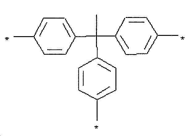
상술한 바와 같이, 에폭시 잔기는 코어 단위로부터 펜던트되어 있고, 이는 중합체성 또는 비중합체성일 수 있다. 하나 이상의 실시양태에서, 코어 단위는 화학식 
하나 이상의 실시양태에서, 코어 단위는 화학식 
하나 이상의 실시양태에서, 코어 단위는 화학식 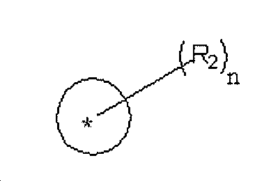


하나 이상의 실시양태에서, 다관능성 에폭시 화합물은 비중합체성 소분자, 단독중합체 및 2개 이하의 상이한 공단량체의 공중합체로 이루어진 그룹으로부터 선택된다. 달리 말하면, 일부 실시양태에서, 삼원중합체, 사원중합체 등은 바람직하게는 본 발명에서의 사용으로부터 제외된다.In one or more embodiments, the multifunctional epoxy compound is selected from the group consisting of non-polymeric small molecules, homopolymers and copolymers of up to two different comonomers. In other words, in some embodiments, terpolymers, quaternary polymers, and the like are preferably excluded from use in the present invention.
상기 실시양태와 관련없이, 다관능성 에폭시 화합물은 반사-방지 코팅 등과 같이 마이크로리소그래피 공정에서 사용하기 위한 조성물의 제조에 이용될 수 있다. 상기 조성물은 다관능성 에폭시 화합물(들)을 바람직하게는 주위 조건에서 실질적으로 균질한 혼합물을 형성하기에 충분한 시간 동안 적합한 용매 시스템에 단순히 분산 또는 용해시킴으로써 형성된다. 바람직한 조성물은, 조성물의 총 중량 100중량%에 기초하여, 약 0.2 내지 50중량%의 다관능성 에폭시 화합물, 바람직하게는 약 0.2 내지 10중량%의 다관능성 에폭시 화합물 및 보다 바람직하게는 약 0.2 내지 4중량%의 다관능성 에폭시 화합물을 포함한다. 상술한 바와 같이, 다관능성 에폭시 화합물은 바람직하게는 반사-방지 조성물에의 사용 전에 여과된다. 따라서, 조성물 중의 미반응 촉매의 수준은 실질적으로 감소된다. 하나 이상의 실시양태에서, 반사-방지 조성물은, 조성물의 총 중량 100중량%에 기초하여, 약 0.01중량% 미만의 잔류 촉매, 및 보다 바람직하게는 약 0.001중량% 미만의 촉매를 포함할 것이다.Regardless of the above embodiments, multifunctional epoxy compounds can be used in the preparation of compositions for use in microlithography processes, such as anti-reflective coatings and the like. The composition is formed by simply dispersing or dissolving the polyfunctional epoxy compound (s) in a suitable solvent system for a time sufficient to form a substantially homogeneous mixture, preferably at ambient conditions. Preferred compositions are from about 0.2 to 50% by weight of a polyfunctional epoxy compound, preferably from about 0.2 to 10% by weight of a polyfunctional epoxy compound and more preferably from about 0.2 to 4% by weight, based on 100% by weight of the total weight of the composition. Weight percent polyfunctional epoxy compound. As described above, the polyfunctional epoxy compound is preferably filtered prior to use in an anti-reflective composition. Thus, the level of unreacted catalyst in the composition is substantially reduced. In one or more embodiments, the anti-reflective composition will include less than about 0.01% by weight residual catalyst, and more preferably less than about 0.001% by weight catalyst, based on 100% by weight of the total weight of the composition.
용매 시스템은 마이크로전자 제조에서의 사용에 적합한 임의의 용매를 포함할 수 있다. 바람직하게는, 용매 시스템은 약 100℃ 내지 약 200℃의 비점을 갖는다. 하나 이상의 실시양태에서, 프로필렌 글리콜 모노메틸 에테르(PGME), 프로필렌 글리콜 모노메틸 에테르 아세테이트(PGMEA), 에틸 락테이트, 프로필렌 글리콜 n-프로필 에테르(PnP), 사이클로헥산온, 감마 부티롤락톤(GBL) 및 이들의 혼합물로 이루어진 그룹으로부터 선택된 용매를 포함할 것이다. 용매 시스템은, 조성물의 총 중량 100중량%에 기초하여, 약 75 내지 약 99.8중량%, 및 바람직하게는 약 95 내지 99.5중량%의 수준으로 조성물에서 사용된다. 조성물의 총 고체는, 조성물의 총 중량 100중량%에 기초하여, 약 0.2 내지 약 25중량%, 및 바람직하게는 약 0.5 내지 약 5중량% 범위이어야 한다.The solvent system can include any solvent suitable for use in microelectronic manufacturing. Preferably, the solvent system has a boiling point of about 100 ° C to about 200 ° C. In one or more embodiments, propylene glycol monomethyl ether (PGME), propylene glycol monomethyl ether acetate (PGMEA), ethyl lactate, propylene glycol n-propyl ether (PnP), cyclohexanone, gamma butyrolactone (GBL) And solvents selected from the group consisting of mixtures thereof. The solvent system is used in the composition at a level of about 75 to about 99.8% by weight, and preferably about 95 to 99.5% by weight, based on 100% by weight of the total weight of the composition. The total solids of the composition should range from about 0.2 to about 25 weight percent, and preferably from about 0.5 to about 5 weight percent, based on 100 weight percent of the total weight of the composition.
조성물은 또한 바람직하게는 가교결합제를 포함한다. 일부 실시양태에서, 조성물은 가교결합제와 함께 용매 시스템에 분산 또는 용해된 다관능성 에폭시 화합물로 실질적으로 이루어지거나 심지어 이루어진다. 특히 바람직한 가교결합제는 비닐 에테르 가교결합제이다. 가교결합제가 다관능성(예: 이관능성, 삼관능성 및 사관능성)인 것이 특히 바람직하다. 가교결합제는, 조성물의 총 중량 100중량%에 기초하여, 약 0.1 내지 약 10중량% 및 바람직하게는 약 0.2 내지 약 1중량%의 수준으로 조성물에 바람직하게 존재한다.The composition also preferably comprises a crosslinking agent. In some embodiments, the composition consists substantially or even of a multifunctional epoxy compound dispersed or dissolved in a solvent system with a crosslinking agent. Particularly preferred crosslinking agents are vinyl ether crosslinking agents. It is particularly preferred that the crosslinking agent is polyfunctional (eg, bifunctional, trifunctional and tetrafunctional). The crosslinking agent is preferably present in the composition at a level of about 0.1 to about 10% by weight and preferably about 0.2 to about 1% by weight, based on 100% by weight of the total weight of the composition.
보다 바람직하게는, 예시적 비닐 에테르 가교결합제는 화학식 R'-(R4-O-CH=CH2)n(여기서, R'는 아릴(바람직하게는 C6-C14) 및 알킬(바람직하게는 C1-C18, 및 보다 바람직하게는 C1-C10)로 이루어진 그룹으로부터 선택되고, R4는 각각 개별적으로 알킬(바람직하게는 C1-C18, 및 보다 바람직하게는 C1-C10), 알콕시(바람직하게는 C1-C18, 및 보다 바람직하게는 C1-C10), 카보닐 및 이들의 2종 이상의 배합물로 이루어진 그룹으로부터 선택되고, n은 적어도 2, 및 바람직하게는 2 내지 6이다)을 갖는다. 가장 바람직한 비닐 에테르는 에틸렌 글리콜 비닐 에테르, 트리메틸올프로판 트리비닐 에테르, 1,4-사이클로헥산 디메탄올 디비닐 에테르 및 이들의 혼합물로 이루어진 그룹으로부터 선택된 것들을 포함한다. 또 다른 바람직한 비닐 에테르는 More preferably, exemplary vinyl ether crosslinkers are of formula R '-(R 4 -O-CH = CH 2 ) n (where R' is aryl (preferably C 6 -C 14 ) and alkyl (preferably Is selected from the group consisting of C 1 -C 18 , and more preferably C 1 -C 10 ), R 4 are each individually alkyl (preferably C 1 -C 18 , and more preferably C 1- C 10 ), alkoxy (preferably C 1 -C 18 , and more preferably C 1 -C 10 ), carbonyl, and two or more combinations thereof, wherein n is at least 2, and preferably Is 2 to 6). Most preferred vinyl ethers include those selected from the group consisting of ethylene glycol vinyl ether, trimethylolpropane trivinyl ether, 1,4-cyclohexane dimethanol divinyl ether and mixtures thereof. Another preferred vinyl ether is


반사-방지 조성물은 또한 산 발생제(예: 광산 발생제("PAG"), 열적 산 발생제("TAG")), 염기 퀀쳐, 계면활성제, 확산 촉진제, 완충제 등과 같은 추가의 임의 성분을 추가로 포함할 수 있다. 예를 들면, PAG는, 이들이 193nm 및/또는 248nm 및/또는 365nm 방사선에 감수성인 한, 이온성 또는 비이온성인 것이 선택될 수 있다. 이온성 PAG는 설포늄 및/또는 요오도늄 염을 함유하는 것들로부터 선택될 수 있다. 카운터 이온은 트리플레이트, 노나플레이트, 메티드, 이미드, 캄포르설포네이트, 또는 방사선에 노광시킬 때에 강산을 발생시킬 수 있는 것들로부터 선택될 수 있다. 비이온성 PAG는 트리아진, 나프틸이미드, 디아조메탄, 디설폰 및/또는 설포네이트를 포함할 수 있다. 존재하는 경우, PAG는, 조성물의 총 중량 100중량%에 기초하여, 약 0.01 내지 약 0.5중량%의 수준으로 조성물에 사용되어야 한다. 일부 실시양태에서, 반사-방지 조서물은 가교결합제 및 PAG와 함께 용매 시스템에 분산 또는 용해된 다관능성 에폭시 화합물로 본질적으로 이루어지거나 심지어 이루어진다. 일부 실시양태에서, 반사-방지 조성물은 바람직하게는 산 발생제(PAG 및/또는 TAG)를 실질적으로 포함하지 않는다. 즉, 반사-방지 조성물은 바람직하게는 약 0.01중량% 미만의 산 발생제, 보다 바람직하게는 약 0.005중량% 미만의 산 발생제 및 보다 바람직하게는 약 0중량%의 산 발생제를 포함한다. 이러한 실시양태에서, 상술한 바와 같이, 반사-방지 코팅은 조성물을 탈가교결합 반응을 개시하여 현상제-가용성으로 되게 하기 위해 스택 내의 다른 층으로부터 산 확산에 의존한다.Anti-reflective compositions also add additional optional ingredients such as acid generators (eg, photoacid generators ("PAG"), thermal acid generators ("TAG"), base quenchers, surfactants, diffusion promoters, buffers, etc. It can contain as. For example, PAGs can be selected to be ionic or nonionic, as long as they are sensitive to 193nm and / or 248nm and / or 365nm radiation. The ionic PAG can be selected from those containing sulfonium and / or iodonium salts. The counter ion can be selected from triflate, nonaplate, methide, imide, camphorsulfonate, or those capable of generating a strong acid when exposed to radiation. Nonionic PAGs can include triazine, naphthylimide, diazomethane, disulfone and / or sulfonate. If present, PAG should be used in the composition at a level of about 0.01 to about 0.5% by weight, based on 100% by weight of the total weight of the composition. In some embodiments, the anti-reflective formulation consists essentially of or even consists of a polyfunctional epoxy compound dispersed or dissolved in a solvent system with a crosslinker and PAG. In some embodiments, the anti-reflective composition is preferably substantially free of acid generators (PAG and / or TAG). That is, the anti-reflective composition preferably comprises less than about 0.01% by weight acid generator, more preferably less than about 0.005% by weight acid generator and more preferably about 0% by weight acid generator. In this embodiment, as described above, the anti-reflective coating relies on acid diffusion from other layers in the stack to initiate the decrosslinking reaction to make the composition developer-soluble.
본 발명에 사용하기 위한 퀀쳐는 트리에탄올아민 또는 트리옥틸아민 등과 같은 아민 함유 그룹으로부터 선택될 수 있다. 기타 퀀쳐는 t-boc-보호된 것, 예를 들면, t-boc-보호된 아미노산, 광염기 발생제 또는 광분해가능한 염기일 수 있다. 존재하는 경우, 퀀쳐는, 조성물의 총 중량 100중량%에 기초하여, 약 0.001 내지 약 2중량%, 및 바람직하게는 약 0.01 내지 약 0.5중량%의 수준으로 조성물에 사용될 수 있다. 반사-방지 조성물은 퀀쳐를 실질적으로 포함하지 않을 수 있다. 이러한 실시양태에서, 조성물은, 조성물의 총 중량 100중량%에 기초하여, 바람직하게는 약 0.0001중량% 미만의 퀀쳐, 보다 바람직하게는 약 0.00005중량% 미만의 퀀쳐를 포함한다.The quencher for use in the present invention can be selected from amine containing groups such as triethanolamine or trioctylamine. Other quenchers can be t-boc-protected, such as t-boc-protected amino acids, photobase generators or photodegradable bases. When present, the quencher can be used in the composition at a level of from about 0.001 to about 2% by weight, and preferably from about 0.01 to about 0.5% by weight, based on 100% by weight of the total weight of the composition. The anti-reflective composition may be substantially free of quencher. In this embodiment, the composition comprises, based on 100% by weight of the total weight of the composition, preferably less than about 0.0001% by weight of a quencher, more preferably less than about 0.00005% by weight of a quencher.
반사-방지 조성물로부터 바람직하게 제외되는 추가 성분은 다관능성 에폭시 화합물, 결합제 수지 등 이외에 기타 중합체 또는 올리고머를 포함한다.Additional components that are preferably excluded from anti-reflective compositions include other polymers or oligomers in addition to polyfunctional epoxy compounds, binder resins, and the like.
이미 언급한 바와 같이, 조성물은 마이크로전자 제조에서 현상제-가용성 반사-방지 코팅으로서 특히 유용하다. 예를 들면, 반사-방지 코팅은 소정량의 반사-방지 조성물을 마이크로전자 기판에 도포하여 기판 표면 상에 조성물 층을 형성함으로써 형성될 수 있다. 조성물은 기판 표면에 직접 도포되거나, 기판 표면 위에 형성된 하나 이상의 광학 중간 하도층의 최상층에 도포될 수 있다. 적합한 중간 하도층은 탄소-풍부 층(예: 스핀-온 탄소 층(SOC), 무정형 탄소 층), 편광 층, 실리콘 하드마스크 층, 갭-충전 층 및 이들의 조합으로 이루어진 그룹으로부터 선택된 것들을 포함한다. 용어 "탄소-풍부"는, 본원에서 사용된 바와 같이, 조성물 중의 총 고체 100중량%에 기초하여, 약 50중량% 초과의 탄소, 바람직하게는 약 70중량% 초과의 탄소 및 보다 바람직하게는 약 75 내지 약 80중량%의 탄소를 포함하는 조성물을 지칭한다.As already mentioned, the composition is particularly useful as a developer-soluble anti-reflective coating in microelectronic manufacturing. For example, an anti-reflective coating can be formed by applying a predetermined amount of an anti-reflective composition to a microelectronic substrate to form a composition layer on the substrate surface. The composition may be applied directly to the substrate surface, or may be applied to the top layer of one or more optical intermediate underlayers formed over the substrate surface. Suitable intermediate underlayers include those selected from the group consisting of carbon-rich layers (eg spin-on carbon layers (SOC), amorphous carbon layers), polarizing layers, silicon hardmask layers, gap-filling layers and combinations thereof. . The term "carbon-rich", as used herein, based on 100% by weight of the total solids in the composition, more than about 50% by weight of carbon, preferably more than about 70% by weight of carbon and more preferably about Refers to a composition comprising 75 to about 80 weight percent carbon.
임의의 마이크로전자 기판을 본 발명에서 사용할 수 있다. 바람직한 기판은 실리콘, SiGe, SiO2, Si3N4, 알루미늄, 텅스텐, 규화텅스텐, 비화갈륨, 게르마늄, 탄탈륨, 질화탄탈륨, 산호, 블랙 다이아몬드, 인 또는 붕소 도핑된 유리, 이온 주입 층, 질화티탄, 산화하프늄, 산질화실리콘 및 이들의 혼합물로 이루어진 그룹으로부터 선택된 것들을 포함한다. 조성물은 임의의 공지된 도포 방법으로 도포할 수 있고, 한 가지 바람직한 방법은 조성물을 약 750rpm 내지 약 5,000rpm(바람직하게는 약 750rpm 내지 약 4,000rpm 및 보다 바람직하게는 약 1,000rpm 내지 약 3,500rpm)의 속도로 약 20초 내지 약 90초(바람직하게는 약 30초 내지 약 60초)의 기간 동안 스핀-코팅하는 것이다. 기판은 평탄한 표면을 가질 수 있거나, 표면형태(topography) 특징(홀, 트렌치, 콘택트 홀, 융기 특징, 라인 등)을 포함할 수 있다. 본원에 사용된 바와 같이, "표면형태"는 기판 표면 내에 또는 표면 상에서 구조체의 높이 또는 깊이를 지칭한다. 예를 들면, 기판은, 측벽 및 하부 벽을 포함하는 홀을 획정하는 구조체를 포함할 수 있다. 따라서, 반사-방지 조성물을 기판에 도포하는 방법은 바람직하게는 조성물을 이들 홀 측벽 및 하부 벽의 적어도 일부분에 도포하는 것을 포함한다.Any microelectronic substrate can be used in the present invention. Preferred substrates are silicon, SiGe, SiO 2 , Si 3 N 4 , aluminum, tungsten, tungsten silicide, gallium arsenide, germanium, tantalum, tantalum nitride, coral, black diamond, phosphorus or boron doped glass, ion implantation layer, titanium nitride , Hafnium oxide, silicon oxynitride, and mixtures thereof. The composition can be applied by any known application method, one preferred method is to apply the composition from about 750 rpm to about 5,000 rpm (preferably from about 750 rpm to about 4,000 rpm and more preferably from about 1,000 rpm to about 3,500 rpm) Spin-coating for a period of about 20 seconds to about 90 seconds (preferably about 30 seconds to about 60 seconds) at a rate of. The substrate may have a flat surface, or may include topography features (holes, trenches, contact holes, raised features, lines, etc.). As used herein, “surface form” refers to the height or depth of a structure in or on a substrate surface. For example, the substrate can include a structure that defines a hole that includes a side wall and a bottom wall. Accordingly, the method of applying the anti-reflective composition to the substrate preferably includes applying the composition to at least a portion of these hole sidewalls and bottom walls.
목적하는 도포범위가 달성된 후, 조성물은 가열하여 열 가교결합을 유도함으로써 경화된 반사-방지 코팅을 형성할 수 있다. 층은 바람직하게는 적어도 약 80℃, 바람직하게는 약 125℃ 내지 약 230℃, 및 보다 바람직하게는 약 130℃ 내지 약 250℃의 온도로 약 5초 내지 약 90초(바람직하게는 약 30초 내지 약 60초)의 기간 동안 가열된다. 유리하게는, 반사-방지 층의 경화는 조성물 중의 다관능성 에폭시 화합물의 가교결합을 수반한다. 다관능성 에폭시 화합물의 가교결합은 개환된 에폭시 잔기 상의 유리 -OH 그룹을 통해서 뿐만 아니라 화합물 중 발색단 상의 가교결합성 그룹을 통해 발생할 수 있다. 본 발명은 열적 가교결합을 수반하고, 화합물의 가교결합을 개시하기 위해 산 또는 TAG를 필요로 하지 않는다. 산 발생제는, 조성물에 존재하는 경우, 하기에 보다 상세히 논의된 바와 같이, 단지 화합물의 탈가교결합에 관여한다.After the desired coverage is achieved, the composition can be heated to induce thermal crosslinking to form a cured anti-reflective coating. The layer is preferably from about 5 seconds to about 90 seconds (preferably about 30 seconds) at a temperature of at least about 80 ° C, preferably about 125 ° C to about 230 ° C, and more preferably about 130 ° C to about 250 ° C. To about 60 seconds). Advantageously, curing of the anti-reflection layer involves crosslinking of the polyfunctional epoxy compound in the composition. Crosslinking of the polyfunctional epoxy compound can occur not only through the free -OH group on the opened epoxy moiety, but also through the crosslinkable group on the chromophore in the compound. The present invention involves thermal crosslinking and does not require an acid or TAG to initiate crosslinking of the compound. The acid generator, when present in the composition, is only involved in the decrosslinking of the compound, as discussed in more detail below.
베이킹 후에 반사-방지 층의 평균 두께는 바람직하게는 약 20nm 내지 약 100nm, 보다 바람직하게는 약 20nm 내지 약 75nm 및 보다 더 바람직하게는 약 20nm 내지 약 60nm이다. 기판 표면이 표면형태를 포함하는 경우, 반사-방지 코팅은 바람직하게는 이들 두께에서 기판 표면형태를 실질적으로 피복하기에 충분한 두께로 도포된다. 평균 두께는 타원계에 의해 수득한 기판의 5개 측정치의 평균으로 정의도니다.The average thickness of the anti-reflection layer after baking is preferably about 20 nm to about 100 nm, more preferably about 20 nm to about 75 nm and even more preferably about 20 nm to about 60 nm. If the substrate surface comprises a surface morphology, the anti-reflective coating is preferably applied at these thicknesses to a thickness sufficient to substantially cover the substrate surface morphology. The average thickness is also defined as the average of five measurements of the substrate obtained by an ellipsometer.
본 발명에 따르는 경화된 감광성 내식막에 통상 사용되는 용매(예: 에틸 락테이트, PGME)에 실질적으로 불용성일 것이다. 따라서, 박리 시험에 제공하는 경우, 본 발명의 코팅은 약 5% 미만, 바람직하게는 약 1% 미만 및 보다 더 바람직하게는 약 0%의 박리율을 가질 것이다. 박리 시험은 먼저 경화된 층의 평균 두께(5개의 상이한 위치에서 측정치의 평균을 취함으로써)를 측정하는 것을 수반한다. 이는 평균 초기 필름 두께이다. 이어서, 용매(예: PGME)를 경화된 필름에 약 20초 동안 퍼들링한 다음, 약 3,000rpm에서 약 30초 동안 스핀 건조시켜 용매를 제거한다. 두께는 타원계를 사용하여 웨이퍼의 5개 상이한 지점에서 다시 측정하고, 이들 측정치의 평균을 결정한다. 이는 평균 최종 필름 두께이다. 박리의 정도는 초기 및 최종 평균 필름 두께 사이에서 상이하다. 박리율은 다음과 같다:It will be substantially insoluble in solvents (eg ethyl lactate, PGME) commonly used in the cured photoresist according to the invention. Thus, when provided for a peel test, the coating of the present invention will have a peel rate of less than about 5%, preferably less than about 1% and even more preferably about 0%. The peel test involves first measuring the average thickness of the cured layer (by taking the average of the measurements at five different locations). This is the average initial film thickness. Subsequently, a solvent (eg, PGME) is pudded to the cured film for about 20 seconds, followed by spin drying at about 3,000 rpm for about 30 seconds to remove the solvent. The thickness is again measured at five different points on the wafer using an ellipsometer and the average of these measurements is determined. This is the average final film thickness. The degree of delamination differs between the initial and final average film thickness. The peel rate is as follows:
% 박리 = (박리 정도/초기 평균 필름 두께) × 100% Peel = (degree of peeling / initial average film thickness) × 100
경화된 반사-방지 코팅은 또한 바람직하게는 통상의 감광성 내식막 현상제(예: 테르라메틸암모늄 하이드록사이드(TMAH))에 실질적으로 불용성이다. 현상제 중의 본 발명 필름의 용해도는 상기한 박리 시험의 것과 동일한 공정 및 계산을 사용하여 평가하고, 다만 감광성 내식막 용매 대신에 알칼리 현상제를 사용한다. 가교결합된 층은 또한 110℃에서 60초 동안 PEB로 처리한다. 이어서, 0.26N TMAH 현상제를 상기 층 위에 45초 동안 퍼들링한 다음, 5초간 탈이온수로 세정하고, 스핀 건조시킨다. 경화된 층에서 임의의 두께 손실은 "암 손실(dark loss)"로 정의된다. 경화된 층은 약 5% 미만, 바람직하게는 약 1.5% 미만, 보다 더 바람직하게는 약 1% 미만, 보다 더 바람직하게는 약 0.8% 미만 및 가장 바람직하게는 약 0%의 암 손실을 가질 것이다.The cured anti-reflective coating is also preferably substantially insoluble in conventional photoresist resists (eg terramethylammonium hydroxide (TMAH)). The solubility of the film of the present invention in the developer is evaluated using the same process and calculation as that of the peel test described above, but an alkali developer is used instead of the photosensitive corrosion resistant solvent. The crosslinked layer was also treated with PEB at 110 ° C. for 60 seconds. Then, 0.26N TMAH developer was pudded on the layer for 45 seconds, followed by washing with deionized water for 5 seconds and spin drying. Any thickness loss in the cured layer is defined as “dark loss”. The cured layer will have a cancer loss of less than about 5%, preferably less than about 1.5%, even more preferably less than about 1%, even more preferably less than about 0.8% and most preferably about 0%. .
필름의 습식 현상은 또한 박리 시험의 것과 유사한 공정 및 계산을 사용하여 평가할 수 있다. 경화된 층은 오리엘 DUV 광대역 노광 장치 상에서 광대역 광으로 20mJ/cm2에서 먼저 노광시킨다. 이어서, 노광된 층은 130℃에서 90초 동안 PEB에 제공한다. 이어서, 감광성 내식막 현상제(0.26N TMAH)를 60초 동안 필름에 퍼들링하고, 이어서 300rpm으로 회전시키면서 5초간 탈이온수로 세정하고, 이어서 약 30초 동안 약 3,000rpm으로 스핀 건조시켜 현상제를 제거한다. 층의 두께를 다시 측정하고, 현상제 %를 계산한다. 감광성의 현상제-가용성 반사-방지 코팅(PAG를 갖는)은 바람직하게는 약 95% 내지 약 100% 및 보다 바람직하게는 약 99% 내지 약 100%의 현상제 %를 가질 것이다.The wet development of the film can also be assessed using processes and calculations similar to those of the peel test. The cured layer is first exposed at 20 mJ / cm 2 with broadband light on an Oriel DUV broadband exposure apparatus. The exposed layer is then applied to the PEB at 130 ° C. for 90 seconds. Subsequently, the photoresist developer (0.26N TMAH) was pudded to the film for 60 seconds, then washed with deionized water for 5 seconds while rotating at 300 rpm, and then spin dried at about 3,000 rpm for about 30 seconds to develop the developer. Remove it. The thickness of the layer is measured again, and the% developer is calculated. The photosensitive developer-soluble anti-reflective coating (with PAG) will preferably have about 95% to about 100% and more preferably about 99% to about 100% developer%.
경화된 반사-방지 코팅의 n 값(복소굴절률의 실수 성분)은 적어도 약 1.3, 바람직하게는 약 1.4 내지 약 2, 보다 바람직하게는 약 1.45 내지 약 2, 보다 바람직하게는 약 1.45 내지 약 1.8 및 보다 더 바람직하게는 약 1.5 내지 약 1.75일 것이다.The n value (real component of the complex refractive index) of the cured anti-reflective coating is at least about 1.3, preferably about 1.4 to about 2, more preferably about 1.45 to about 2, more preferably about 1.45 to about 1.8 and Even more preferably from about 1.5 to about 1.75.
반사-방지 코팅은 또한 바람직하게는 사용 파장(예: 193nm, 248nm, 또는 365nm)에서 적어도 약 0.2, 바람직하게는 약 0.25 내지 약 0.65, 및 보다 바람직하게는 약 0.3 내지 약 0.6의 k 값(복소굴절률의 허수 성분)을 갖는다.The anti-reflective coating also preferably has a k value (complex) of at least about 0.2, preferably about 0.25 to about 0.65, and more preferably about 0.3 to about 0.6 at the wavelength of use (eg, 193 nm, 248 nm, or 365 nm). Imaginary component of the refractive index).
이어서, 감광성 조성물을 본 발명의 층에 도포한 다음, 도포후 베이킹(PAB)하여 영상화 층을 형성할 수 있다. 영상화 층의 두께는 통상 약 50nm 내지 약 2,000nm 범위일 것이다. 적합한 영상화 조성물은 상업적으로 입수가능한 감광성 내식막[예: TOK사의 TarF-Pi6-001, Kawasaki shi, Kanagawa (Japan); JSR 마이크로(JSR Micro)사의 ARX3001JN, ARX3340J 및 AM2073J, Sunnyvale, CA; SAIL-X-181, Shin-Etsu, Tokyo (Japan)] 또는 임의의 기타 감광성 조성물을 포함한다. 반사-방지 코팅 조성물은 본질적으로 감광성이 아닌 경우(즉, PAG-보다 적은 반사-방지 코팅), 적합한 감광성 조성물은 바람직하게는 산 발생제(바람직하게는 PAG)를 포함하고, 하기에 보다 상세히 설명된 바와 같이, 이를 현상제-가용성으로 되게 하기 위해 인접한 반사-방지 코팅을 탈가교결합 및 탈보호하는 충분한 산을 발생시킬 수 있다. 유리하게는, 본 발명에 따른 반사-방지 코팅은 얇은 층을 형성하기 위해 사용되어, 인접한 감광성 내식막으로부터의 산 확산은 반사-방지 코팅의 전체 두께에 걸쳐 확산할 수 있고 패턴은, 기판 또는, 존재하는 경우, 중간층에 이르기까지 명료할 수 있다.Subsequently, the photosensitive composition may be applied to the layer of the present invention and then baked (PAB) after application to form an imaging layer. The thickness of the imaging layer will typically range from about 50 nm to about 2,000 nm. Suitable imaging compositions include commercially available photoresist films (eg, TarF-Pi6-001 from TOK, Kawasaki shi, Kanagawa (Japan); ARX3001JN, ARX3340J and AM2073J from JSR Micro, Sunnyvale, CA; SAIL-X-181, Shin-Etsu, Tokyo (Japan)] or any other photosensitive composition. If the anti-reflective coating composition is not essentially photosensitive (i.e. less anti-reflective coating than PAG-), a suitable photosensitive composition preferably comprises an acid generator (preferably PAG), described in more detail below. As can be done, it can generate enough acid to decrosslink and deprotect adjacent anti-reflective coatings to make it developer-soluble. Advantageously, the anti-reflective coating according to the invention is used to form a thin layer, so that acid diffusion from adjacent photosensitive resists can diffuse over the entire thickness of the anti-reflective coating and the pattern can be a substrate, or, If present, it can be clear down to the middle layer.
영상화 층은 마스크를 통해 적절한 파장(193nm 내지 365nm)의 광에 노광시키고, 이어서 노광후 베이킹(PEB) 및 패턴의 현상에 의해 패턴화될 수 있다. 적합한 현상제는 유기 또는 무기 알칼리 용액, 예를 들면, 수산화칼륨(KOH), TMAH이고, 바람직하게는 0.26N 이하의 농도로 TMAH의 수용액을 포함한다. 이들 현상제의 일부는 상표명 PD523AD[모제스 레이크 인더스트리즈 인코포레이티드(Moses Lake Industries, Inc.)사에서 입수가능, Moses Lake, WA], MF-319[(다우 케미칼(Dow Chemical)사에서 입수가능], MF-320[시플레이(Shipley)사에서 입수가능] 및 NMD3[티오케이(TOK)사에서 입수가능, Japan]로 상업화되어 있다.The imaging layer can be patterned by exposure to light of an appropriate wavelength (193 nm to 365 nm) through a mask, followed by post-exposure baking (PEB) and pattern development. A suitable developer is an organic or inorganic alkali solution, for example potassium hydroxide (KOH), TMAH, and preferably includes an aqueous solution of TMAH at a concentration of 0.26 N or less. Some of these developers are trade names PD523AD (available from Moses Lake Industries, Inc., Moses Lake, WA), MF-319 (available from Dow Chemical Commercially available], MF-320 (available from Shipley) and NMD3 (available from TOKAY, Japan).
또 다른 실시양태에서, ArF 침지 리소그래피는 영상화 층을 패턴화하기 위해 사용될 수 있다. 공기(통상의 리소그래피에서와 같이) 대신에, 노광 동안 방사선이 통과하는 매질은 액체이다. 영상화 층은 리소그래피 시스템의 광학 투영 부재(즉, 렌즈)를 통해 방사선에 노광되고, 이때 침지 액체는 리소그래피 시스템의 광학 부재의 적어도 일부분 및 구조체(즉, 스택)의 일부분과 접촉한다. 보다 바람직하게는, 액체는 광학 부재는 액체에 침지되도록 시스템의 최종 광학 부재와 영상화 층 사이를 충전한다. 적합한 침지 액체는 바람직하게는 1 초과(바람직하게는 약 1 내지 약 2 및 보다 바람직하게는 약 1.3 내지 약 1.4)의 굴절률을 갖고, 물(바람직하게는 정제수) 및 유기 용매로 이루어진 그룹으로부터 선택된다. 침지 리소그래피 시스템은 당해 기술분야에 공지되어 있고, 암피비안 시스템(Amphibian Systems; Rochester, NY)사의 암피비안 인터페로미터(Amphibian Interferometer) 및 ASML(Veldhoven, Netherlands)사의 1900i를 포함한다.In another embodiment, ArF immersion lithography can be used to pattern the imaging layer. Instead of air (as in conventional lithography), the medium through which radiation passes during exposure is liquid. The imaging layer is exposed to radiation through an optical projection member (ie lens) of the lithography system, where the immersion liquid contacts at least a portion of the optical member of the lithography system and a portion of the structure (ie stack). More preferably, the liquid fills between the final optical element of the system and the imaging layer so that the optical element is immersed in the liquid. Suitable immersion liquids preferably have a refractive index greater than 1 (preferably from about 1 to about 2 and more preferably from about 1.3 to about 1.4) and are selected from the group consisting of water (preferably purified water) and organic solvents. . Immersion lithography systems are known in the art and include Amphibian Interferometer from Amphibian Systems (Rochester, NY) and 1900i from Veldhoven, Netherlands (ASML).
이와 상관없이, 영상화 층은 적절한 파장의 광에 대한 노광, 이어서 영상화 층의 노광된 부분의 현상 및 제거(포지티브-작업 영상화 층의 경우에)에 의해 패턴화된다. 유리하게는, 영상화 층이 광에 노광되면, 본 발명의 반사-방지 코팅이 된다. 광에 노광시키면, 산은 산 발생제(반사-방지 코팅 자체에서 또는 영상화 층으로부터)로부터 발생되고, 이러한 산은 반사-방지 코팅 층에서 다관능성 에폭시 화합물 및 비닐 에테르 가교결합제를 "탈가교결합"시킨다. 즉, 반사-방지 코팅이 본래적으로 감광성이 아닌 경우에도, 반사-방지 코팅의 노광된 부분은 영상화 층의 노광된 부분으로부터 영상화 층에 인접하는 반사-방지 코팅의 상응하는 부분으로의 산 확산에 의해 광에의 노광시에 여전히 현상제-가용성으로 된다. 산(영상화 층 또는 반사-방지 코팅으로부터든지)은 열적 가교결합시에 반사-방지 코팅에서 다관능성 에폭시 화합물과 가교결합제 사이 및 특히 가교결합성 발색단과 가교결합제 사이에 형성되는 결합을 파괴한다. 탈가교결합은 조성물을 현상제-가용성으로 되게 하는 발색단 상에 가교결합성 그룹을 포함하는 다관능성 에폭시 화합물을 재생시킨다.Regardless, the imaging layer is patterned by exposure to light of an appropriate wavelength, followed by development and removal (in the case of a positive-working imaging layer) of the exposed portion of the imaging layer. Advantageously, when the imaging layer is exposed to light, it becomes the anti-reflective coating of the present invention. Upon exposure to light, the acid is generated from an acid generator (either in the anti-reflective coating itself or from the imaging layer), and this acid "decrosslinks" the polyfunctional epoxy compound and the vinyl ether crosslinker in the anti-reflective coating layer. That is, even if the anti-reflective coating is not inherently photosensitive, the exposed portion of the anti-reflective coating is subjected to acid diffusion from the exposed portion of the anti-reflective layer to the corresponding portion of the anti-reflective coating adjacent the imaging layer. This still renders the developer-soluble upon exposure to light. The acid (either from the imaging layer or the anti-reflective coating), upon thermal cross-linking, breaks the bonds formed between the polyfunctional epoxy compound and the cross-linker in the anti-reflective coating, and in particular between the cross-linkable chromophore and the cross-linker. Decrosslinking regenerates a multifunctional epoxy compound comprising a crosslinkable group on the chromophore that renders the composition developer-soluble.
이어서, 상기 공정에 의해 가용성으로 된 영상화 층 및 반사-방지 코팅의 노광된 부분을 현상제와 접촉시켜 노광된 부분을 제거한다. 영상화 층의 노광된 부분의 하부에 있는 반사-방지 코팅의 노광된 부분은, 영상화 층 및 반사-방지 코팅 층에서 목적하는 패턴을 동시에 형성하도록 영상화 층이 제거될 때에 현상제에 의해 제거된다. 패턴은 습식 및/또는 건식 에칭 및/또는 이온 주입 공정을 사용하여 궁극적으로 기판으로 전사될 수 있는 홀, 트렌치, 라인, 공간 등을 통한 것이다. 바람직하게는, 반사-방지 코팅의 노광된 부분의 적어도 약 95%는 현상제에 의해 제거될 것이고, 보다 바람직하게는 적어도 약 99% 및 보다 더 바람직하게는 약 100%가 제거될 것이다. 본 발명의 코팅은, 이들이 노공 및 베이킹시에 실질적으로 완전히 탈가교결합되어, 생성되는 패턴이 기판 또는, 존재하는 경우, 중간 층에 이르기까지 완전히 명료화될 수 있다는 점에서 독특한 잇점을 제공한다. 달리 말하면, 반사-방지 코팅의 노광된 부분은 패턴화된 특징에 잔류하는 매우 소량의 반사-방지 조성물 잔류물로 바람직하게는 완전히 제거된다. 특히, 약 5nm 미만의 반사-방지 코팅 두께가 노광된 부분에 잔류하고, 바람직하게는 약 1nm 미만, 보다 바람직하게는 0.5nm 미만의의 반사-방지 코팅 두께가 노광된 부분에 잔류한다.The exposed portion of the imaging layer and anti-reflective coating rendered soluble by the above process is then contacted with the developer to remove the exposed portion. The exposed portion of the anti-reflective coating underlying the exposed portion of the imaging layer is removed by the developer when the imaging layer is removed to simultaneously form the desired pattern in the imaging layer and anti-reflective coating layer. The pattern is through holes, trenches, lines, spaces, etc., which can ultimately be transferred to a substrate using wet and / or dry etching and / or ion implantation processes. Preferably, at least about 95% of the exposed portion of the anti-reflective coating will be removed by the developer, more preferably at least about 99% and even more preferably about 100%. The coatings of the present invention offer a unique advantage in that they are substantially completely decrosslinked during labor and baking, so that the resulting pattern can be fully clarified down to the substrate or, if present, the intermediate layer. In other words, the exposed portion of the anti-reflective coating is preferably completely removed with a very small amount of anti-reflective composition residue remaining in the patterned features. In particular, an anti-reflective coating thickness of less than about 5 nm remains in the exposed portion, preferably an anti-reflective coating thickness of less than about 1 nm, more preferably less than 0.5 nm remains in the exposed portion.
하나 이상의 실시양태에서, 반사-방지 층의 노광된 부분은 상기 기재된 바와 같이 노광 후에 현상제를 가용성으로 되게 하기 때문에, 개구부는 영상화 층의 현상 동안 반사-방지 층에 형성된다. 따라서, 영상화 층의 리소그래피 패턴화는 영상화 층 및 반사-방지 층 둘 다에서 개구부(예를 들면, 콘택트 홀, 비아 홀, 트렌치 등)을 형성한다. 개구부는 서로 연통한다(즉, 기판 또는, 존재하는 경우, 중간 층이 피복되지 않거나 노출되도록 적어도 어느 정도로 정렬되어 있다). 추가로, 처리는 기판 또는 중간 층의 노광된 부분 위에서 수행할 수 있거나, 패턴을 기판 표면으로 전사할 수 있다.In one or more embodiments, the openings are formed in the anti-reflection layer during development of the imaging layer, because the exposed portion of the anti-reflection layer renders the developer soluble after exposure as described above. Thus, lithographic patterning of the imaging layer forms openings (eg, contact holes, via holes, trenches, etc.) in both the imaging layer and the anti-reflection layer. The openings communicate with each other (ie, at least to some extent so that the substrate or, if present, the intermediate layer is uncovered or exposed). Additionally, the treatment can be performed on the exposed portion of the substrate or intermediate layer, or the pattern can be transferred to the substrate surface.
예를 들면, 이온은 노광된 기판으로 주입될 수 있다. 이온 주입을 위해, 이온은 공지된 공정을 사용하여 이온 공급원에 의해 도펀트로부터 생성된다. 본 발명에서 사용하기에 바람직한 일부 이온은 원소주기율표의 제III족 내지 제V족 원소의 이온으로 이루어진 그룹으로부터 선택된 것들이고, 붕소, 질소, 인, 비소, 이불화붕소, 인듐, 안티몬, 게르마늄, 실리콘, 탄소 및 갈륨의 이온이 특히 바람직하다. 다른 바람직한 이온은 수소, 아르곤, 베릴륨, 불소, 산소 및 헬륨으로 이루어진 그룹으로부터 선택된다. 생성된 이온은 당해 이온이 기판을 침투할 수 있는 충분히 높은 에너지 수준으로 가속된다. 바람직한 에너지 수준은 약 1eV 내지 약 20MeV, 바람직하게는 약 5 KeV 내지 약 2,000KeV, 및 보다 바람직하게는 약 20KeV 내지 약 500KeV이다. 통상의 이온 선량은 약 10원자/cm2 내지 약 10e30원자/cm2, 및 보다 바람직하게는 약 1e12원자/cm2 내지 약 1e16원자/cm2일 수 있다. 가속된 이온은 공지된 방법으로 초점을 맞춘다. 이러한 한 가지 공정은 빔이 목적하는 직경에 도달할 때까지 일련의 정전기 및 자기 렌즈를 사용하는 것을 수반한다. 이어서, 빔은 기판으로 지향된다. 당해 기술분야의 당업자에게 이해되는 바와 같이, 빔의 각도는 기판에서 이온 깊이를 조절하기 위해 조정될 수 있다. 현상후에 잔류하는 영상화 층 및 반사-방지 층의 노광되지 않은 부분은 이온이 요구되지 않는 기판 부분을 보호하기 위해 사용되고, 패턴의 개구부는 이온에 의한 기판으로의 접근을 제공한다. 결과적으로, 주입 부분은 패턴에 상응하는 기판에 형성될 수 있다. 개구부의 수, 크기 및 형상은 필요에 따라 조정되어, 최종 용도에 적절한 위치에서 이온을 기판에 주입할 수 있는 것으로 이해된다.For example, ions can be implanted into the exposed substrate. For ion implantation, ions are produced from dopants by ion sources using known processes. Some ions preferred for use in the present invention are those selected from the group consisting of ions of Groups III to V elements of the Periodic Table of the Elements, boron, nitrogen, phosphorus, arsenic, boron fluoride, indium, antimony, germanium, silicon , Carbon and gallium ions are particularly preferred. Other preferred ions are selected from the group consisting of hydrogen, argon, beryllium, fluorine, oxygen and helium. The ions produced are accelerated to a level of energy high enough to allow them to penetrate the substrate. Preferred energy levels are from about 1 eV to about 20 MeV, preferably from about 5 KeV to about 2,000 KeV, and more preferably from about 20 KeV to about 500 KeV. Typical ion doses may be from about 10 atoms / cm 2 to about 10e 30 atoms / cm 2 , and more preferably from about 1e 12 atoms / cm 2 to about 1e 16 atoms / cm 2 . The accelerated ions are focused in a known manner. One such process involves using a series of electrostatic and magnetic lenses until the beam reaches the desired diameter. The beam is then directed to the substrate. As will be appreciated by those skilled in the art, the angle of the beam can be adjusted to adjust the ion depth in the substrate. The unexposed portions of the imaging layer and anti-reflection layer remaining after development are used to protect the portion of the substrate where ions are not required, and the opening of the pattern provides access to the substrate by ions. As a result, the injection portion can be formed on the substrate corresponding to the pattern. It is understood that the number, size, and shape of the openings can be adjusted as needed, allowing ions to be implanted into the substrate at locations suitable for the end use.
본원 명세서의 다양한 실시양태의 추가의 잇점은 본원 명세서 및 하기 실시예를 검토하면 당업자에게 명백해질 것이다. 본원에 기재된 다양한 실시양태는, 본원에서 달리 지시되지 않는 한, 반드시 상호 배타적인 것은 아닌 것으로 이해된다. 예를 들면, 한 가지 실시양태에서 기재 또는 제시된 특징은 또한 다른 실시양태에 포함될 수 있지만, 반드시 포함되는 것은 아니다. 따라서, 본 발명은 본원에 기재된 특정 실시양태의 다양한 조합 및/또는 총합을 포함한다. 또한, 도면이 설명되어 있고 명세서가 특정의 바람직한 실시양태를 기재하고 있지만, 이러한 개시는 단지 일례인 것으로 이해되어야 한다.Additional advantages of various embodiments of the present specification will become apparent to those skilled in the art upon review of the present specification and the examples below. It is understood that the various embodiments described herein are not necessarily mutually exclusive unless otherwise indicated herein. For example, features described or presented in one embodiment may also be included in other embodiments, but are not necessarily included. Accordingly, the present invention includes various combinations and / or sums of the specific embodiments described herein. In addition, although the drawings have been described and the specification describes certain preferred embodiments, it should be understood that this disclosure is merely an example.
본원에 사용된 바와 같이, 문구 "및/또는"은, 2개 이상의 항목 목록에 사용되는 경우, 수록된 목록 중의 어느 하나가 자체로 사용되거나 수록된 목적의 2개 이상의 임의의 조합이 사용될 수 있는 것을 의미한다. 예를 들면, 조성물이 성분 A, B 및/또는 C를 함유하거나 배제하는 것으로 기재되어 있는 경우, 당해 조성물은 A 단독; B 단독; C 단독; A와 B 조합; A와 C 조합; B와 C 조합; 또는 A, B 및 C 조합을 함유하거나 배제할 수 있다.As used herein, the phrase “and / or”, when used in a list of two or more items, means that any of the listed lists may be used by itself or any combination of two or more of the listed purposes may be used. do. For example, if the composition is described as containing or excluding components A, B and / or C, the composition may be composed of A alone; B alone; C alone; A and B combinations; A and C combination; B and C combination; Or A, B and C combinations.
본 기재는 또한 수치 범위를 사용하여 본 발명의 다양한 실시양태에 관한 특정한 파라미터를 정량화한다. 수치 범위가 제공되는 경우, 이러한 범위는, 당해 범위의 상한치를 단지 인용하는 청구범위 제한 뿐만 아니라 당해 범위의 하한치를 단지 인용하는 청구범위 제한에 대한 문헌적 서포트를 제공하는 것으로 해석됨을 이해해야 한다. 예를 들면, 약 10 내지 약 100의 개시된 수치 범위는 "약 10 초과"(상한 범위 없음)를 인용하는 청구범위 및 "약 100 미만"(하한치 없음)을 인용하는 청구범위에 대한 문헌적 서포트를 제공한다.
The description also uses numerical ranges to quantify specific parameters relating to various embodiments of the invention. It should be understood that where numerical ranges are provided, such ranges are to be construed as providing literature support not only for the claims limitations citing only the upper limit of the range, but also for the claims limitations only citing the lower limit of the range. For example, the disclosed numerical ranges of about 10 to about 100 provide literature support for claims citing "above about 10" (no upper limit) and claims citing "below about 100" (no lower limit). to provide.
실시예Example
하기 실시예는 본 발명에 따르는 방법을 기재한다. 그러나, 이들 실시예는 예시를 위해 제공되며, 본원의 어떤 것도 본 발명의 전체 범위에 대한 한정으로서 제공되지 않는 것으로 이해되어야 한다.
The following examples describe the method according to the invention. However, it should be understood that these examples are provided for illustrative purposes, and that nothing here is provided as a limitation on the entire scope of the present invention.
실시예 1Example 1
2,3-트리스(에폭시프로필)이소시아누레이트와 3,7-디하이드록시-2-나프토산의 반응Reaction of 2,3-tris (epoxypropyl) isocyanurate and 3,7-dihydroxy-2-naphthoic acid

3구 500mL 플라스크에 자기 교반 바, 질소 유입구, 질소 배출구를 갖는 응축기 및 온도계를 장착시켰다. 플라스크에 236.26g의 사이클로헥산온(Harcros Chemical, St. Louis, MO), 65.0625g의 3,7-디하이드록시-2-나프토산(Sigma Aldrich, St. Louis, MO), 34.3125g의 2,3-트리스(에폭시프로필)이소시아누레이트(Nissan Chemical Industries, Tokyo, Japan) 및 1.8908g의 벤질트리에틸암모늄 클로라이드(BTEAC; Lancaster Synthesis, Ward Hill, MA)를 충전시켰다. 반응물을 120℃로 가열시키고, 24시간 동안 교반시킨 다음, 주위 조건으로 냉각시켰다. 냉각 후, 반응 생성물을 50.625g의 AMBERSEP 200H 수지(Rohm and Haas, Philadelphia, PA)와 혼합하고, 4시간 동안 회전시켰다. 4시간 후, 200H 수지를 여과에 의해 제거했다.
A three-neck 500 mL flask was equipped with a magnetic stir bar, a nitrogen inlet, a condenser with a nitrogen outlet, and a thermometer. To the flask 236.26 g cyclohexanone (Harcros Chemical, St. Louis, MO), 65.0625 g 3,7-dihydroxy-2-naphthoic acid (Sigma Aldrich, St. Louis, MO), 34.3125 g 2, 3-tris (epoxypropyl) isocyanurate (Nissan Chemical Industries, Tokyo, Japan) and 1.8908 g of benzyltriethylammonium chloride (BTEAC; Lancaster Synthesis, Ward Hill, MA) were charged. The reaction was heated to 120 ° C., stirred for 24 hours, and then cooled to ambient conditions. After cooling, the reaction product was mixed with 50.625 g of AMBERSEP 200H resin (Rohm and Haas, Philadelphia, PA) and spun for 4 hours. After 4 hours, 200H resin was removed by filtration.
실시예 2Example 2
실시예 1로부터의 화합물을 사용한 현상제-가용성 하부 반사-방지 코팅 배합물Developer-soluble bottom anti-reflective coating formulation using the compound from Example 1
감광성 하부 반사-방지 코팅 배합물은 실시예 1의 화합물을 사용하여 제조했다. 배합물은 125mL 호박색 날겐(Amber Nalgene) 병에 3.5587g의 실시예 1의 반응 생성물, 0.4270g의 비닐 에테르 가교결합제 LIVELinkTM(Brewer Science, Inc, Rolla, MO), 0.0053g의 트리에탄올아민(Sigma Aldrich, St. Louis, MO), 94.56g의 PGME(Harcros Chemical, St. Louis, MO) 및 1.4489g의 사이클로헥산온을 충전시켜 제조했다. 혼합물을 밤새 와동시킨 다음, 청정한 125mL 호박색 날겐 병으로 0.1㎛ 종점 필터를 통해 여과했다. The photosensitive bottom anti-reflective coating formulation was prepared using the compound of Example 1. The formulation is 3.5587 g of the reaction product of Example 1, 0.4270 g of vinyl ether crosslinker LIVELink TM (Brewer Science, Inc, Rolla, MO), 0.0053 g of triethanolamine (Sigma Aldrich, in a 125 mL Amber Nalgene bottle) St. Louis, MO), 94.56 g of PGME (Harcros Chemical, St. Louis, MO) and 1.4489 g of cyclohexanone. The mixture was vortexed overnight, then filtered through a 0.1 μm end filter into a clean 125 mL amber raw bottle.
감광성 하부 반사-방지 코팅 물질은 실리콘 웨이퍼 상에서 1,500rpm으로 스핀-코팅한 다음, 160℃에서 60초 동안 베이킹시켰다. 필름을 에틸 락테이트(Harcros, St. Louis, MO)로 세정하여 필름의 용매 내성을 시험한 다음, 암 손실을 평가하기 위해 노광 없이 감광성 내식막 현상제, PD523AD(JSR Micro, Sunnyvale, CA)에 침지시켰다. 또 다른 제조된 웨이퍼 상에서, 콘트라스트 곡선은 오리엘 DUV 광대역 노광 툴 및 248nM 밴드 패스 필터를 사용하여 시험했다. 콘트라스트 노광 후, PEB는 125℃에서 90초 동안 수행했고, 웨이퍼는 PD523AD를 사용하여 45초 동안 현상시킨 다음, 탈이온수로 5초 동안 세정하고, 건식 스피닝시켰다. 표 1은 그 결과를 요약한 것이다.The photosensitive bottom anti-reflective coating material was spin-coated at 1,500 rpm on a silicon wafer and then baked at 160 ° C. for 60 seconds. The film was washed with ethyl lactate (Harcros, St. Louis, MO) to test the solvent resistance of the film, and then to a photosensitive resist developer without exposure to PD523AD (JSR Micro, Sunnyvale, CA) to evaluate cancer loss. Immersed. On another manufactured wafer, the contrast curve was tested using an Oriel DUV broadband exposure tool and a 248nM band pass filter. After the contrast exposure, PEB was performed at 125 ° C. for 90 seconds, and the wafer was developed using PD523AD for 45 seconds, then washed with deionized water for 5 seconds and dry-spinned. Table 1 summarizes the results.
(암 손실)Develop without exposure
(Cancer loss)
이들 결과는 이러한 물질이 우수한 용매 내성 및 최소 암 손실을 보유하고, 여전히 노광후 알칼리 현상제에서 완전히 제거될 수 있음을 나타낸다.These results indicate that this material has good solvent resistance and minimal cancer loss and can still be completely removed from the alkali developer after exposure.
이어서, 상기 배합물을 실리콘 웨이퍼 상에 스핀-코팅하고, 160℃에서 60초 동안 베이킹시켰다. 이어서, 반사-방지 코팅을, 90초 동안 130℃의 PAB 및 90초 동안 125℃의 PEB와 함께, 248nm 리소그래피(JSR M529Y 내식막)용의 감광성 내식막으로 코팅시켰다. 도 1은 리소그래피 결과를 나타낸다.
The blend was then spin-coated on a silicon wafer and baked at 160 ° C. for 60 seconds. The anti-reflective coating was then coated with a photoresist for 248 nm lithography (JSR M529Y resist) with PAB at 130 ° C. for 90 seconds and PEB at 125 ° C. for 90 seconds. 1 shows the lithography results.
실시예 3Example 3
3,7-디하이드록시-2-나프톨산과 폴리(페닐 글리시딜 에테르-코-포름알데히드)의 반응Reaction of 3,7-dihydroxy-2-naphtholic acid with poly (phenyl glycidyl ether-co-formaldehyde)

3구 100mL 플라스크에 자기 교반 바, 질소 유입구, 질소 배출구를 갖는 응축기 및 온도계를 장착시켰다. 플라스크에 387.89g의 사이클로헥산온, 87.11g의 3,7-디하이드록시-2-나프토산, 76.75g의 폴리(페닐 글리시딜 에테르-코-포름알데히드)(Sigma Aldrich, St. Louis, MO) 및 2.38g의 벤질트리메틸암모늄 클로라이드(BTMAC; Sigma Aldrich, St. Louis, MO)를 충전시켰다. 반응물을 120℃로 가열하고, 24시간 동안 교반시킨 다음, 주위 조건으로 냉각시켰다. 냉각 후, 반응 생성물을 83.1195g의 AMBERSEP 200H 수지 및 83.1195g의 Dowex 550A 수지(Sigma Aldrich, St. Louis, MO)와 혼합하고, 24시간 동안 회전시켰다. 24시간 후, 수지를 여과에 의해 제거했다.
A three-neck 100 mL flask was equipped with a magnetic stir bar, a nitrogen inlet, a nitrogen condenser and a thermometer. In a flask 387.89 g cyclohexanone, 87.11 g 3,7-dihydroxy-2-naphthoic acid, 76.75 g poly (phenyl glycidyl ether-co-formaldehyde) (Sigma Aldrich, St. Louis, MO ) And 2.38 g of benzyltrimethylammonium chloride (BTMAC; Sigma Aldrich, St. Louis, MO). The reaction was heated to 120 ° C., stirred for 24 hours, and then cooled to ambient conditions. After cooling, the reaction product was mixed with 83.1195g AMBERSEP 200H resin and 83.1195g Dowex 550A resin (Sigma Aldrich, St. Louis, MO) and spun for 24 hours. After 24 hours, the resin was removed by filtration.
실시예 4Example 4
실시예 3의 중합체를 사용한 현상제-가용성 하부 반사-방지 코팅 배합물Developer-soluble bottom anti-reflective coating formulation using the polymer of Example 3
감광성 하부 반사-방지 코팅 배합물은 실시예 3의 중합체를 사용하여 제조했다. 당해 배합물은 125mL 호박색 날겐 병에 3.5638g의 실시예 3의 반응 생성물, 0.4277g의 비닐 에테르 가교결합제 LIVELinkTM, 0.0032g의 트리에탄올아민, 94.56g의 PGME 및 1.4489g의 사이클로헥산올을 충전시킴으로써 제조했다. 혼합물을 밤새 와동시킨 다음, 청정한 125mL 호박색 날겐 병에서 0.1㎛ 종점 필터를 통해 여과했다.The photosensitive bottom anti-reflective coating formulation was prepared using the polymer of Example 3. This formulation was prepared by filling a 125 mL amber nalgen bottle with 3.5638 g of the reaction product of Example 3, 0.4277 g of vinyl ether crosslinker LIVELink ™ , 0.0032 g of triethanolamine, 94.56 g of PGME and 1.4489 g of cyclohexanol. . The mixture was vortexed overnight, then filtered through a 0.1 μm endpoint filter in a clean 125 mL amber raw bottle.
감광성 하부 반사-방지 코팅을 실리콘 웨이퍼 상으로 1,500rpm에서 스핀-코팅시킨 다음, 160℃에서 60초 동안 베이킹시켰다. 필름을 에틸 락테이트로 세정하여 필름의 용매 내성을 시험한 다음, 노광 없이 감광성 내식막 현상제, PD523AD에 침지시켜 암 손실을 평가했다. 또 다른 제조된 웨이퍼 상에서, 감광성 내식막, JSR M529Y을 감광성 하부 반사-방지 코팅의 상부에 1,500rpm에서 스핀-코팅시킨 다음, 130℃에서 90초 동안 베이킹시켰다. 콘트라스트 곡선은 오리엘 DUV 광대역 노광 툴 및 248nm 밴드 통과 필터를 사용하여 시험했다. 콘트라스트 노광 후, PEB는 125℃에서 90초 동안 수행하고, 웨이퍼는 45초 동안 PD523AD를 사용하여 현상시킨 다음, 탈이온수로 5초 동안 세정하고, 건식 스피닝시켰다. 표 2는 그 결과를 요약한 것이다.The photosensitive bottom anti-reflective coating was spin-coated on a silicon wafer at 1,500 rpm and then baked at 160 ° C. for 60 seconds. The film was washed with ethyl lactate to test the solvent resistance of the film, and then immersed in a photosensitive resist developer, PD523AD, without exposure to evaluate cancer loss. On another manufactured wafer, a photosensitive resist, JSR M529Y, was spin-coated at 1,500 rpm on top of the photosensitive bottom anti-reflective coating, and then baked at 130 ° C. for 90 seconds. Contrast curves were tested using an Oriel DUV broadband exposure tool and a 248nm band pass filter. After the contrast exposure, PEB was performed at 125 ° C. for 90 seconds, and the wafer was developed using PD523AD for 45 seconds, then washed with deionized water for 5 seconds and dry-spinned. Table 2 summarizes the results.
이 결과는, 이러한 물질이 우수한 용매 내성 및 최소 암 손실을 보유하고, 여전히 노광 후에 알칼리 현상제에서 완전히 제거될 수 있음을 나타낸다.The results show that these materials have good solvent resistance and minimal dark loss and can still be completely removed from the alkali developer after exposure.
이어서, 상기 배합물을 실리콘 웨이퍼 상으로 스핀-코팅하고, 160℃에서 60초 동안 베이킹시켰다. 이어서, 반사-방지 코팅을, 90초 동안 130℃의 PAB 및 90초 동안 125℃의 PEB와 함께, 248nm 리소그래피(JSR M529Y 내식막)용의 감광성 내식막으로 코팅시켰다. 도 2는 이 리소그래피 결과를 나타낸다.
The blend was then spin-coated onto a silicon wafer and baked at 160 ° C. for 60 seconds. The anti-reflective coating was then coated with a photoresist for 248 nm lithography (JSR M529Y resist) with PAB at 130 ° C. for 90 seconds and PEB at 125 ° C. for 90 seconds. 2 shows the results of this lithography.
실시예 5Example 5
글리시딜 메타크릴레이트 및 스티렌의 중합반응, 이어서 3,7-디하이드록시-2-나프토산의 부착Polymerization of glycidyl methacrylate and styrene followed by attachment of 3,7-dihydroxy-2-naphthoic acid

3구 250-mL 플라스크에 자기 교반 바, 질소 유입구, 질소 배출구를 갖는 응축기 및 온도계를 장착시켰다. 폴리(글리시딜 메타크릴레이트-코-스티렌)은 플라스크에 115.00g의 사이클로헥산올, 25.0g의 스티렌(Sigma Aldrich, St. Louis, MO), 50.0g의 글리시딜 메타크릴레이트(Sigma Aldrich, St. Louis, MO), 1.875g의 1-도데칸티올 및 3.75g의 2,2'-아조비스(2-메틸프로피오니트릴)(Sigma Aldrich, St. Louis, MO)을 충전시킴으로써 제조했다. 반응물을 75℃로 가열하고, 18시간 동안 교반시킨 다음, 주위 조건으로 냉각시켰다. 냉각 후, 중합체를 에탄올 및 n-헥산의 50/50 블렌드(Sigma Aldrich, St. Louis, MO)로 침전시킨 다음, 진공 오븐에서 40℃로 48시간 동안 건조시켰다.A three-neck 250-mL flask was equipped with a magnetic stir bar, a nitrogen inlet, a condenser with a nitrogen outlet, and a thermometer. Poly (glycidyl methacrylate-co-styrene) was placed in a flask with 115.00 g of cyclohexanol, 25.0 g of styrene (Sigma Aldrich, St. Louis, MO), and 50.0 g of glycidyl methacrylate (Sigma Aldrich) , St. Louis, MO), 1.875 g of 1-dodecanthiol and 3.75 g of 2,2'-azobis (2-methylpropionitrile) (Sigma Aldrich, St. Louis, MO). . The reaction was heated to 75 ° C., stirred for 18 hours, and then cooled to ambient conditions. After cooling, the polymer was precipitated with a 50/50 blend of ethanol and n-hexane (Sigma Aldrich, St. Louis, MO) and then dried in a vacuum oven at 40 ° C. for 48 hours.
자기 교반 바, 질소 유입구, 질소 배출구를 갖는 응축기 및 온도계를 장착시킨 제2 3구 250-mL 플라스크에 23.50g의 무수 제조한 폴리(글리시딜 메타크릴레이트-코-스티렌), 20.23g의 3,7-디하이드록시-2-나프토산, 0.146g의 벤질트리메틸암모늄 클로라이드(Sigma Aldrich, St. Louis, MO) 및 102.0g의 사이클로헥산온을 충전시켰다. 반응물을 120℃로 가열시키고, 6시간 동안 교반시켰다. 냉각되면, 100.0g의 반응 생성물을 20.0g의 사이클로헥산온으로 희석시켰다. 희석된 용액을 18.0g의 AMBERSEP 200H 수지 및 18.0g의 Dowex 550A 수지(Sigma Aldrich, St. Louis, MO)와 24시간 동안 혼합했다. 24시간 후, 수지는 여과에 의해 제거했다.
23.50 g of anhydrous prepared poly (glycidyl methacrylate-co-styrene) in a second three-neck 250-mL flask equipped with a magnetic stir bar, nitrogen inlet, condenser with nitrogen outlet, and thermometer, 20.23 g of 3 , 7-dihydroxy-2-naphthoic acid, 0.146 g of benzyltrimethylammonium chloride (Sigma Aldrich, St. Louis, MO) and 102.0 g of cyclohexanone were charged. The reaction was heated to 120 ° C. and stirred for 6 hours. Upon cooling, 100.0 g of the reaction product was diluted with 20.0 g of cyclohexanone. The diluted solution was mixed with 18.0 g of AMBERSEP 200H resin and 18.0 g of Dowex 550A resin (Sigma Aldrich, St. Louis, MO) for 24 hours. After 24 hours, the resin was removed by filtration.
실시예 6Example 6
실시예 5의 중합체를 사용한 현상제-가용성 하부 반사-방지 코팅 배합물Developer-soluble bottom anti-reflective coating formulation using the polymer of Example 5
감광성 하부 반사-방지 코팅 배합물은 실시예 5의 중합체를 사용하여 제조했다. 당해 배합물은 60mL 호박색 날겐 병에 2.2956g의 실시예 5의 반응 생성물, 0.1722g의 비닐 에테르 가교결합제 LIVELinkTM, 0.0172g의 TPS-C1(Daychem Laboratories, Inc., Vandalia, OH), 0.0017g의 트리에탄올아민, 41.5809g의 PGME 및 0.9324g의 사이클로헥산온을 충전시킴으로써 제조했다. 혼합물을 밤새 와동시킨 다음, 청정한 60mL 호박색 날겐 병으로 0.1㎛ 종점 필터를 통해 여과했다.The photosensitive bottom anti-reflective coating formulation was prepared using the polymer of Example 5. This formulation contained 2.2956 g of the reaction product of Example 5, 0.1722 g of vinyl ether crosslinker LIVELink ™ , 0.0172 g of TPS-C1 (Daychem Laboratories, Inc., Vandalia, OH), 0.0017 g of triethanol in a 60 mL amber Naalgen bottle. It was prepared by filling amine, 41.5809 g PGME and 0.9324 g cyclohexanone. The mixture was vortexed overnight, and then filtered through a 0.1 μm end filter into a clean 60 mL amber raw bottle.
감광성 하부 반사-방지 코팅을 실리콘 웨이퍼 상에서 1,500rpm으로 스핀-코팅시킨 다음, 160℃에서 60초 동안 베이킹시켰다. 필름을 에틸 락테이트로 세정하여 필름의 용매 내성을 시험한 다음, 노광 없이 감광성 내식막 현상제, PD523AD에 침지시켜 암 손실을 평가했다. 또 다른 제조된 웨이퍼 상에서, 콘트라스트 곡선은 오리엘 DUV 광대역 노광 툴 및 248nm 밴트 통과 필터를 사용하여 시험했다. 콘트라스트 노광 후, PEB를 125℃에서 90초 동안 수행하고, 웨이퍼를 45초 동안 PD523AD를 사용하여 현상시킨 다음, 탈이온수로 5초간 세정하고 건식 스피닝시켰다. 표 3은 그 결과를 요약한 것이다.The photosensitive bottom anti-reflective coating was spin-coated at 1,500 rpm on a silicon wafer and then baked at 160 ° C. for 60 seconds. The film was washed with ethyl lactate to test the solvent resistance of the film, and then immersed in a photosensitive resist developer, PD523AD, without exposure to evaluate cancer loss. On another fabricated wafer, the contrast curve was tested using an Oriel DUV broadband exposure tool and a 248nm vent pass filter. After contrast exposure, PEB was performed at 125 ° C. for 90 seconds, and the wafer was developed using PD523AD for 45 seconds, followed by washing with deionized water for 5 seconds and dry spinning. Table 3 summarizes the results.
(암 손실)Develop without exposure
(Cancer loss)
(내식막 사용)Exposure, PEB and development
(Use of resist film)
이 결과는 이러한 물질이 우수한 용매 내성 및 최소 암 손실을 보유하고, 여전히 노광 후에 알칼리 현상제에서 완전하게 제거될 수 있음을 나타낸다.These results indicate that these materials have good solvent resistance and minimal dark loss, and can still be completely removed from the alkali developer after exposure.
감광성 하부 반사-방지 코팅 배합물을 실리콘 웨이퍼 상에 스핀-코팅시키고, 160℃에서 60초 동안 베이킹시켰다. 이어서, 반사-방지 코팅을, 90초 동안 130℃의 PAB 및 90초 동안 125℃의 PEB와 함께, 248nm 리소그래피(JSR M529Y 내식막)용의 감광성 내식막으로 코팅시켰다. 도 3은 이 리소그래피 결과를 나타낸다.
The photosensitive bottom anti-reflective coating formulation was spin-coated on a silicon wafer and baked at 160 ° C. for 60 seconds. The anti-reflective coating was then coated with a photoresist for 248 nm lithography (JSR M529Y resist) with PAB at 130 ° C. for 90 seconds and PEB at 125 ° C. for 90 seconds. 3 shows the results of this lithography.
실시예 7Example 7
글리시딜 메타크릴레이트 및 스티렌의 중합반응 및 3,7-디하이드록시-2-나프토산의 부착Polymerization of glycidyl methacrylate and styrene and adhesion of 3,7-dihydroxy-2-naphthoic acid
3구 250mL 플라스크에 자기 교반 바, 질소 유입구, 질소 배출구를 갖는 응축기 및 온도계를 장착시켰다. 플라스크에 120g의 사이클로헥산온, 17.78g의 스티렌, 56.64g의 글리시딜 메타크릴레이트, 1.86g의 1-도데칸디올 및 3.72g의 2,2-아조비스(2-메틸프로피오니트릴)을 충전시켰다. 반응물을 75℃로 가열시키고, 18시간 동안 교반한 다음, 주위 조건으로 냉각시켰다. 냉각 후, 중합체 모액을 추가의 처리 없이 병에 수집했다.A three-neck 250 mL flask was equipped with a magnetic stir bar, a nitrogen inlet, and a condenser with a nitrogen outlet and a thermometer. The flask was charged with 120 g cyclohexanone, 17.78 g styrene, 56.64 g glycidyl methacrylate, 1.86 g 1-dodecanediol and 3.72 g 2,2-azobis (2-methylpropionitrile). Charged. The reaction was heated to 75 ° C., stirred for 18 hours, and then cooled to ambient conditions. After cooling, the polymer mother liquor was collected in bottles without further treatment.
자기 교반 바, 질소 유입구, 질소 배출구를 갖는 응축기 및 온도계가 장착된 제2 3구 250mL 플라스크에 64.73g의 제조된 폴리(글리시딜 메타크릴레이트-코-스티렌) 모액, 23.68g의 3,7-디하이드록시-2-나프토산, 0.43g의 벤질트리메틸암모늄 클로라이드 및 111.16g의 사이클로헥산을 충전시켰다. 반응물을 120℃로 가열시키고, 16시간 동안 교반시켰다. 냉각되면, 용액을 24시간 동안 16.0g의 AMBERSEP 200H 수지 및 16.0g의 Dowex 550A 수지(Sigma Aldrich, St. Louis, MO)와 혼합했다. 24시간 후, 수지는 여과에 의해 제거했다.
64.73 g of prepared poly (glycidyl methacrylate-co-styrene) mother liquor, 23.68 g of 3,7 in a second 3-neck 250 mL flask equipped with a magnetic stir bar, nitrogen inlet, condenser with nitrogen outlet and thermometer -Dihydroxy-2-naphthoic acid, 0.43 g of benzyltrimethylammonium chloride and 111.16 g of cyclohexane were charged. The reaction was heated to 120 ° C. and stirred for 16 hours. Upon cooling, the solution was mixed with 16.0 g of AMBERSEP 200H resin and 16.0 g of Dowex 550A resin (Sigma Aldrich, St. Louis, MO) for 24 hours. After 24 hours, the resin was removed by filtration.
실시예 8Example 8
글리시딜 메타크릴레이트 및 스티렌의 중합반응, 이어서 3,7-디하이드록시-2-나프토산의 부착Polymerization of glycidyl methacrylate and styrene followed by attachment of 3,7-dihydroxy-2-naphthoic acid
3구 250mL 플라스크에 자기 교반 바, 질소 유입구, 질소 배출구를 갖는 응축기 및 온도계를 장착시켰다. 당해 플라스크에 120g의 사이클로헥산온, 11.52g의 스티렌, 62.90g의 글리시딜 메타크릴레이트, 1.86g의 1-도데칸티올 및 3.72g의 2,2'-아조비스(2-메틸프로피오니트릴)을 충전시켰다. 반응물을 75℃로 가열시키고, 18시간 동안 교반한 다음, 주위 조건으로 냉각시켰다. 냉각 후, 중합체 모액을 추가의 처리 없이 병에 수집했다.A three-neck 250 mL flask was equipped with a magnetic stir bar, a nitrogen inlet, and a condenser with a nitrogen outlet and a thermometer. To the flask 120 g cyclohexanone, 11.52 g styrene, 62.90 g glycidyl methacrylate, 1.86 g 1-dodecanthiol and 3.72 g 2,2'-azobis (2-methylpropionitrile ) Was charged. The reaction was heated to 75 ° C., stirred for 18 hours, and then cooled to ambient conditions. After cooling, the polymer mother liquor was collected in bottles without further treatment.
자기 교반 바, 질소 유입구, 질소 배출구를 갖는 응축기 및 온도계를 장착시킨 제2 3구 250mL 플라스크에 61.46g의 제조된 폴리(글리시딜 메타크릴레이트-코-스티렌) 모액, 24.96g의 3,7-디하이드록시-2-나프토산, 0.45g의 벤질트리메틸암모늄 클로라이드 및 113.13g의 사이클로헥산온을 충전시켰다. 반응물을 120℃로 가열하고, 16시간 동안 교반시켰다. 냉각되면, 용액을 24시간 동안 16.0g의 AMBERSEP 200H 수지 및 16.0g의 Dowex 550A 수지(Sigma Aldrich, St. Louis, MO)와 혼합했다. 24시간 후, 수지는 여과에 의해 제거했다.
61.46 g of prepared poly (glycidyl methacrylate-co-styrene) mother liquor, 24.96 g of 3,7 in a second 3-neck 250 mL flask equipped with a magnetic stir bar, nitrogen inlet, nitrogen condenser and thermometer -Dihydroxy-2-naphthoic acid, 0.45 g of benzyltrimethylammonium chloride and 113.13 g of cyclohexanone were charged. The reaction was heated to 120 ° C. and stirred for 16 hours. Upon cooling, the solution was mixed with 16.0 g of AMBERSEP 200H resin and 16.0 g of Dowex 550A resin (Sigma Aldrich, St. Louis, MO) for 24 hours. After 24 hours, the resin was removed by filtration.
실시예 9Example 9
글리시딜 메타크릴레이트 단독중합체의 중합반응, 이어서 3,7-디하이드록시-2-나프토산의 부착Polymerization of glycidyl methacrylate homopolymer followed by attachment of 3,7-dihydroxy-2-naphthoic acid

3구 250mL 플라스크에 자기 교반 바, 질소 유입구, 질소 배출구를 갖는 응축기 및 온도계를 장착시켰다. 당해 플라스크에 120g의 사이클로헥산온, 74.42g의 글리시딜 메타크릴레이트, 1.86g의 1-도데칸티올 및 3.72g의 2,2'-아조비스(2-메틸프로피오니트릴)을 충전시켰다. 반응물을 75℃로 가열하고, 18시간 동안 교반한 다음, 주위 온도로 냉각시켰다. 냉각 후, 중합체 모액은 추가의 처리 없이 병에 수집했다.A three-neck 250 mL flask was equipped with a magnetic stir bar, a nitrogen inlet, and a condenser with a nitrogen outlet and a thermometer. The flask was charged with 120 g of cyclohexanone, 74.42 g of glycidyl methacrylate, 1.86 g of 1-dodecanthiol and 3.72 g of 2,2'-azobis (2-methylpropionitrile). The reaction was heated to 75 ° C., stirred for 18 hours, and then cooled to ambient temperature. After cooling, the polymer mother liquor was collected in a bottle without further treatment.
이어서, 자기 교반 바, 질소 유입구, 질소 배출구를 갖는 응축기 및 온도계를 장착시킨 제2 3구 250mL 플라스크에 56.22g의 제조된 폴리(글리시딜 메타크리레이트) 모액, 27.02g의 3,7-디하이드록시-2-나프토산, 0.49g의 벤질트리메틸암모늄 클로라이드 및 116.27g의 사이클로헥산온을 충전시켰다. 반응물을 120℃로 가열시키고, 16시간 동안 교반시켰다. 냉각되면, 93.0g의 사이클로헥산온을 모액 첨가하여 용액의 점도를 감소시켰다. 이어서, 희석된 용액을 24시간 동안 16.0g의 AMBERSEP 200H 수지 및 16.0g의 Dowex 550A 수지(Sigma Aldrich, St. Louis, MO)와 혼합했다. 24시간 후, 수지는 여과에 의해 제거했다.
Subsequently, 56.22 g of prepared poly (glycidyl methacrylate) mother liquor, 27.02 g of 3,7-di in a second 3-neck 250 mL flask equipped with a magnetic stir bar, nitrogen inlet, nitrogen condenser and thermometer Hydroxy-2-naphthoic acid, 0.49 g of benzyltrimethylammonium chloride and 116.27 g of cyclohexanone were charged. The reaction was heated to 120 ° C. and stirred for 16 hours. Upon cooling, 93.0 g of cyclohexanone was added to the mother liquor to reduce the viscosity of the solution. The diluted solution was then mixed with 16.0 g of AMBERSEP 200H resin and 16.0 g of Dowex 550A resin (Sigma Aldrich, St. Louis, MO) for 24 hours. After 24 hours, the resin was removed by filtration.
실시예 10Example 10
글리시딜 메타크릴레이트 및 3급-부틸 메타크릴레이트의 중합반응, 이어서 3,7-디하이드록시-2-나프토산의 부착Polymerization of glycidyl methacrylate and tert-butyl methacrylate followed by adhesion of 3,7-dihydroxy-2-naphthoic acid

3구 250mL 플라스크에 자기 교반 바, 질소 유입구, 질소 배출구를 갖는 응축기 및 온도계를 장착시켰다. 당해 플라스크에 120g의 사이클로헥산온, 30.0g의 3급-부틸 메타크릴레이트(Sigma Aldrich, St. Louis, MO), 44.98g의 글리시딜 메타크릴레이트, 1.67g의 1-도데칸티올 및 3.35g의 2,2'-아조비스(2-메틸프로피오니트릴)을 충전시켰다. 반응물을 75℃로 가열하고, 18시간 동안 교반한 다음, 주위 온도로 냉각시켰다. 냉각 후, 중합체 모액은 추가의 처리 없이 병에 수집했다.A three-neck 250 mL flask was equipped with a magnetic stir bar, a condenser with a nitrogen inlet, and a nitrogen outlet and a thermometer. The flask was charged with 120 g of cyclohexanone, 30.0 g of tert-butyl methacrylate (Sigma Aldrich, St. Louis, MO), 44.98 g of glycidyl methacrylate, 1.67 g of 1-dodecanethiol and 3.35 g of 2,2'-azobis (2-methylpropionitrile) was charged. The reaction was heated to 75 ° C., stirred for 18 hours, and then cooled to ambient temperature. After cooling, the polymer mother liquor was collected in a bottle without further treatment.
자기 교반 바, 질소 유입구, 질소 배출구를 갖는 응축기 및 온도계를 장착시킨 제2 3구 250mL 플라스크에 71.84g의 제조된 폴리(글리시딜 메타크릴레이트-코-3급-부틸 메타크릴레이트) 모액, 20.89g의 3,7-디하이드록시-2-나프토산, 0.38g의 벤질트리메틸암모늄 클로라이드 및 106.89g의 사이클로헥산온을 충전시켰다. 반응물을 120℃로 가열하고, 16시간 동안 교반시켰다. 냉각되면, 용액을 24시간 동안 16.0g의 AMBERSEP 200H 수지 및 16.0g의 Dowex 550A 수지(Sigma Aldrich, St. Louis, MO)와 혼합했다. 24시간 후, 수지는 여과에 의해 제거했다.71.84 g of prepared poly (glycidyl methacrylate-co-tert-butyl methacrylate) mother liquor in a second three-neck 250 mL flask equipped with a magnetic stir bar, nitrogen inlet, nitrogen condenser and thermometer 20.89 g 3,7-dihydroxy-2-naphthoic acid, 0.38 g benzyltrimethylammonium chloride and 106.89 g cyclohexanone were charged. The reaction was heated to 120 ° C. and stirred for 16 hours. Upon cooling, the solution was mixed with 16.0 g of AMBERSEP 200H resin and 16.0 g of Dowex 550A resin (Sigma Aldrich, St. Louis, MO) for 24 hours. After 24 hours, the resin was removed by filtration.
이어서, 제조된 중합체를 사용하여, 실시예 6과 동일한 공정을 사용하여 감광성의 현상제-가용성 하부 반사-방지 코팅을 배합했다. 반사-방지 조성물은 실리콘 웨이퍼 상으로 스핀 코팅하고, 160℃에서 60초 동안 베이킹한 다음, JSR M529Y 내식막, 90초 동안 130℃ PAB 및 90초 동안 125℃의 PEB를 사용하여 248nm 리소그래피에 의해 처리했다. 도 4는 이 리소그래피 결과를 나타낸다.
Subsequently, using the prepared polymer, a photosensitive developer-soluble lower anti-reflective coating was blended using the same process as in Example 6. The anti-reflective composition was spin coated onto a silicon wafer, baked at 160 ° C. for 60 seconds, and then treated by 248 nm lithography using JSR M529Y resist, 130 ° C. PAB for 90 seconds, and PEB at 125 ° C. for 90 seconds. did. 4 shows the results of this lithography.
실시예 11Example 11
글리시딜 메타크릴레이트 및 p-3급-부톡시카보닐옥시스티렌의 중합반응, 이어서 3,7-디하이드록시-2-나프토산의 부착Polymerization of glycidyl methacrylate and p-tert-butoxycarbonyloxystyrene, followed by adhesion of 3,7-dihydroxy-2-naphthoic acid

3구 250mL 플라스크에 자기 교반 바, 질소 유입구, 질소 배출구를 갖는 응축기 및 온도계를 장착시켰다. 당해 플라스크에 120g의 사이클로헥산온, 38.54g의 p-3급-부톡시카보닐옥시스티렌(Dupont, Wilmington, DE), 37.30g의 글리시딜 메타크릴레이트, 1.39g의 1-도데칸티올 및 2.78g의 2,2'-아조비스(2-메틸프로피오니트릴)을 충전시켰다. 반응물을 75℃로 가열하고, 18시간 동안 교반한 다음, 주위 온도로 냉각시켰다. 냉각 후, 중합체 모액은 추가의 처리 없이 병에 수집했다.A three-neck 250 mL flask was equipped with a magnetic stir bar, a nitrogen inlet, and a condenser with a nitrogen outlet and a thermometer. The flask was charged with 120 g cyclohexanone, 38.54 g p-tert-butoxycarbonyloxystyrene (Dupont, Wilmington, DE), 37.30 g glycidyl methacrylate, 1.39 g 1-dodecanethiol, and 2.78 g of 2,2'-azobis (2-methylpropionitrile) was charged. The reaction was heated to 75 ° C., stirred for 18 hours, and then cooled to ambient temperature. After cooling, the polymer mother liquor was collected in a bottle without further treatment.
이어서, 자기 교반 바, 질소 유입구, 질소 배출구를 갖는 응축기 및 온도계를 장착시킨 제2 3구 250mL 플라스크에 77.47g의 제조된 폴리(글리시딜 메타크릴레이트-코-p-3급-부톡시카보닐옥시스티렌) 모액, 18.68g의 3,7-디하이드록시-2-나프토산, 0.34g의 벤질트리메틸암모늄 클로라이드 및 103.52g의 사이클로헥산온을 충전시켰다. 반응물을 120℃로 가열하고, 16시간 동안 교반시켰다. 냉각되면, 용액을 24시간 동안 16.0g의 AMBERSEP 200H 수지 및 16.0g의 Dowex 550A 수지(Sigma Aldrich, St. Louis, MO)와 혼합했다. 24시간 후, 수지는 여과에 의해 제거했다.
Subsequently, 77.47 g of poly (glycidyl methacrylate-co-p-3 grade-butoxycarbohydrate) was prepared in a second 3-neck 250 mL flask equipped with a magnetic stirring bar, a nitrogen inlet, a nitrogen outlet, and a condenser and a thermometer. Nealoxystyrene) mother liquor, 18.68 g 3,7-dihydroxy-2-naphthoic acid, 0.34 g benzyltrimethylammonium chloride and 103.52 g cyclohexanone were charged. The reaction was heated to 120 ° C. and stirred for 16 hours. Upon cooling, the solution was mixed with 16.0 g of AMBERSEP 200H resin and 16.0 g of Dowex 550A resin (Sigma Aldrich, St. Louis, MO) for 24 hours. After 24 hours, the resin was removed by filtration.
실시예 12Example 12
실시예 11의 중합체를 사용한 감광성의 현상제-가용성 하부 반사-방지 코팅 배합물Photosensitive developer-soluble bottom anti-reflective coating formulation using the polymer of Example 11
감광성의 하부 반사-방지 코팅 배합물은 실시예 11의 중합체를 사용하여 제조했다. 당해 배합물은 60mL 호박색 날겐 병에 2.2472g의 실시예 11의 반응 생성물, 0.1685g의 비닐 에테르 가교결합제 LIVELinkTM, 0.0169g의 TPS-C1(Daychem Laboratories, Inc., Vandalia, OH), 0.0028g의 트리에탄올아민, 46.2950g의 PGME 및 1.2696g의 사이클로헥산온을 충전시킴으로써 제조했다. 혼합물을 밤새 와동시킨 다음, 청정 60mL 호박색 날겐 병에 0.1㎛ 종점 필터를 통해 여과했다.The photosensitive bottom anti-reflective coating formulation was prepared using the polymer of Example 11. This formulation contains 2.2472 g of the reaction product of Example 11, 0.1685 g of a vinyl ether crosslinker LIVELink ™ , 0.0169 g of TPS-C1 (Daychem Laboratories, Inc., Vandalia, OH), 0.0028 g of triethanol in a 60 mL amber Naalgen bottle. It was prepared by filling amine, 46.2950 g PGME and 1.2696 g cyclohexanone. The mixture was vortexed overnight, and then filtered through a 0.1 μm end filter into a clean 60 mL amber raw bottle.
감광성 하부 반사-방지 코팅을 실리콘 웨이퍼 상으로 1,500rpm에서 스핀-코팅한 다음, 160℃에서 60초 동안 베이킹했다. 필름을 에틸 락테이트로 세정하여 필름의 용매 내성을 시험한 다음, 노광 없이 감광성 내식막 현상제, PD523AD에 침지시켜 암 손실을 평가했다. 또 다른 제조된 웨이퍼 상에서, 콘트라스트 곡선은 오리엘 DUV 광대역 노광 툴 및 248nm 밴드 통과 필터를 사용하여 시험했다. 콘트라스트 노광 후, PEB는 125℃에서 90초 동안 수행하고, 웨이퍼는 45초 동안 PD523AD를 사용하여 현상시키고, 이어서 5초 동안 탈이온수로 세청하고 건식 스피닝시켰다. 표 4는 그 결과를 요약한 것이다.The photosensitive bottom anti-reflective coating was spin-coated on a silicon wafer at 1,500 rpm and then baked at 160 ° C. for 60 seconds. The film was washed with ethyl lactate to test the solvent resistance of the film, and then immersed in a photosensitive resist developer, PD523AD, without exposure to evaluate cancer loss. On another manufactured wafer, the contrast curve was tested using an Oriel DUV broadband exposure tool and a 248 nm band pass filter. After the contrast exposure, PEB was performed at 125 ° C. for 90 seconds, and the wafer was developed using PD523AD for 45 seconds, followed by washing with deionized water for 5 seconds and dry spinning. Table 4 summarizes the results.
(암 손실)Develop without exposure
(Cancer loss)
(내식막 사용)Exposure, PEB and development
(Use of resist film)
이 결과는 이러한 물질이 우수한 용매 내성 및 최소 암 손실을 보유하고, 여전히 노광 후에 알칼리 현상제에서 완전하게 제거될 수 있음을 나타낸다.These results indicate that these materials have good solvent resistance and minimal dark loss, and can still be completely removed from the alkali developer after exposure.
감광성 하부 반사-방지 코팅 배합물을 실리콘 웨이퍼 상에 스핀-코팅시키고, 160℃에서 60초 동안 베이킹시켰다. 이어서, 반사-방지 코팅을, 90초 동안 130℃의 PAB 및 90초 동안 125℃의 PEB와 함께, 248nm 리소그래피(JSR M529Y 내식막)용의 감광성 내식막으로 코팅시켰다. 도 5는 리소그래피 결과를 나타낸다.
The photosensitive bottom anti-reflective coating formulation was spin-coated on a silicon wafer and baked at 160 ° C. for 60 seconds. The anti-reflective coating was then coated with a photoresist for 248 nm lithography (JSR M529Y resist) with PAB at 130 ° C. for 90 seconds and PEB at 125 ° C. for 90 seconds. 5 shows the lithography results.
Claims (39)
상기 조성물은 용매 시스템에 분산 또는 용해된 중합체성 다관능성 에폭시 화합물 및 비닐 에테르 가교결합제를 포함하고, 상기 중합체성 다관능성 에폭시 화합물은 폴리[(페닐 글리시딜 에테르)-코-포름알데하이드], 폴리[(o-크레실 글리시딜 에테르)-코-포름알데하이드], 폴리(비스페놀 A-코-에피클로로하이드린)-글리시딜 말단-캡핑된, 폴리(스티렌-코-글리시딜 메타크릴레이트), 폴리(p-3급-부톡시카보닐옥시스티렌-코-글리시딜 메타크릴레이트), 및 폴리(3급-부틸 메타크릴레이트-코-글리시딜 메타크릴레이트)로 이루어진 그룹으로부터 선택되는 공중합체로부터 유도되는 중합체성 코어 단위를 포함하며, 상기 중합체성 다관능성 에폭시 화합물은 이에 결합된 적어도 하나의 가교결합성 발색단을 포함하고, 상기 가교결합성 발색단은 2 내지 10의 가교결합성 그룹을 포함하는, 감광성의 현상제-가용성 반사-방지 조성물.A photosensitive developer-soluble anti-reflective composition for the manufacture of microelectronics,
The composition comprises a polymeric polyfunctional epoxy compound and a vinyl ether crosslinking agent dispersed or dissolved in a solvent system, wherein the polymeric polyfunctional epoxy compound is poly [(phenyl glycidyl ether) -co-formaldehyde], poly [(o-cresyl glycidyl ether) -co-formaldehyde], poly (bisphenol A-co-epichlorohydrin) -glycidyl end-capped, poly (styrene-co-glycidyl methacryl Group), poly (p-tert-butoxycarbonyloxystyrene-co-glycidyl methacrylate), and poly (tert-butyl methacrylate-co-glycidyl methacrylate) And a polymeric core unit derived from a copolymer selected from, wherein the polymeric polyfunctional epoxy compound comprises at least one crosslinkable chromophore bound thereto, and the crosslinkable chromophore crosslinked from 2 to 10 A photosensitive developer-soluble anti-reflective composition comprising a sex group.


여기서, *은 당해 화합물에 대한 결합점이고, y는 각각 0 또는 1이고, X는 각각 상기 가교결합성 발색단이고, L은 각각 개별적으로 아미노, 에테르, 티오, 티오에테르, 하이드라진, 설피네이트, 설포네이트, 설폰아미드, 에스테르, 카보네이트, 카바메이트, 아미드 또는 우레아 결합이고, R은 존재하는 경우, 각각 개별적으로 산소원자 또는 -CH2-이고, R1은 각각 개별적으로 -H, 알킬, 설포네이트, 에스테르, 카보네이트, 카바메이트 또는 이의 관능화된 유도체임.The composition of claim 4, wherein the polymeric polyfunctional epoxy compound comprises at least one epoxy moiety of the formula:
Here, * is a binding point to the compound, y is 0 or 1, X is the crosslinkable chromophore, and L is each independently amino, ether, thio, thioether, hydrazine, sulfinate, sulfonate , Sulfonamide, ester, carbonate, carbamate, amide or urea bond, where R, if present, is each independently an oxygen atom or -CH 2- , and R 1 is each individually -H, alkyl, sulfonate, ester , Carbonate, carbamate or a functionalized derivative thereof.

여기서, R2는 각각 개별적으로 미반응 에폭시 잔기, 또는 화학식


여기서, *은 당해 화합물에 대한 결합점이고, y는 각각 0 또는 1이고, X는 각각 상기 가교결합성 발색단이고, L은 각각 개별적으로 아미노, 에테르, 티오, 티오에테르, 하이드라진, 설피네이트, 설포네이트, 설폰아미드, 에스테르, 카보네이트, 카바메이트, 아미드 또는 우레아 결합이고, R은 존재하는 경우, 각각 개별적으로 산소원자 또는 -CH2-이고, R1은 각각 개별적으로 -H, 알킬, 설포네이트, 에스테르, 카보네이트, 카바메이트 또는 이의 관능화된 유도체임.The composition of claim 8, wherein the polymeric core unit comprises a repeating monomer of the formula:
Here, R 2 are each individually unreacted epoxy residue, or formula
Here, * is a binding point to the compound, y is 0 or 1, X is the crosslinkable chromophore, and L is each independently amino, ether, thio, thioether, hydrazine, sulfinate, sulfonate , Sulfonamide, ester, carbonate, carbamate, amide or urea bond, where R, if present, is each independently an oxygen atom or -CH 2- , and R 1 is each individually -H, alkyl, sulfonate, ester , Carbonate, carbamate or a functionalized derivative thereof.
상기 조성물은 용매 시스템에 분산 또는 용해된 중합체성 다관능성 에폭시 화합물 및 비닐 에테르 가교결합제를 포함하고, 상기 중합체성 다관능성 에폭시 화합물은 이에 결합된 적어도 하나의 가교결합성 발색단을 포함하고, 상기 가교결합성 발색단은 2 내지 10의 가교결합성 그룹을 포함하며,
상기 중합체성 다관능성 에폭시 화합물이 중합체성 코어 단위로부터 펜던트된 복수의 에폭시 잔기를 갖는 중합체성 화합물이며,
상기 중합체성 코어 단위가 하기 화학식의 반복 단량체를 포함하는, 조성물:
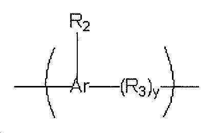
여기서, y는 각각 0 또는 1이고;
Ar은 각각 중합된 아릴 그룹이고;
R2는 각각 개별적으로 미반응 에폭시 잔기, 또는
화학식


여기서, *은 당해 화합물에 대한 결합점이고, y는 각각 0 또는 1이고, X는 각각 상기 가교결합성 발색단이고, L은 각각 개별적으로 아미노, 에테르, 티오, 티오에테르, 하이드라진, 설피네이트, 설포네이트, 설폰아미드, 에스테르, 카보네이트, 카바메이트, 아미드 또는 우레아 결합이고, R은 존재하는 경우, 각각 개별적으로 산소원자 또는 -CH2-이고, R1은 각각 개별적으로 -H, 알킬, 설포네이트, 에스테르, 카보네이트, 카바메이트 또는 이의 관능화된 유도체이고;
R3은 존재하는 경우, 각각 -CH2-임.A photosensitive developer-soluble anti-reflective composition for the manufacture of microelectronics,
The composition includes a polymeric polyfunctional epoxy compound and a vinyl ether crosslinking agent dispersed or dissolved in a solvent system, and the polymeric polyfunctional epoxy compound includes at least one crosslinkable chromophore bound thereto, and the crosslinking Sex chromophores contain 2 to 10 crosslinkable groups,
The polymeric polyfunctional epoxy compound is a polymeric compound having a plurality of epoxy moieties pendant from a polymeric core unit,
The polymeric core unit comprises a repeating monomer of the formula:
Where y is 0 or 1, respectively;
Ar is each polymerized aryl group;
R 2 are each individually unreacted epoxy moieties, or
Chemical formula
Here, * is a binding point to the compound, y is 0 or 1, X is the crosslinkable chromophore, and L is each independently amino, ether, thio, thioether, hydrazine, sulfinate, sulfonate , Sulfonamide, ester, carbonate, carbamate, amide or urea bond, where R, if present, is each independently an oxygen atom or -CH 2- , and R 1 is each individually -H, alkyl, sulfonate, ester , Carbonate, carbamate or a functionalized derivative thereof;
When R 3 is present, each is -CH 2- .
R'-(R4-O-CH=CH2)n,
여기서, R'는 아릴 및 알킬로 이루어진 그룹으로부터 선택되고, R4는 각각 개별적으로 알킬, 알콕시, 카보닐 및 이들의 2종 이상의 조합으로 이루어진 그룹으로부터 선택되고, n은 적어도 2임.The composition of claim 1, wherein the vinyl ether crosslinking agent is a polyfunctional vinyl ether of the formula:
R '-(R 4 -O-CH = CH 2 ) n ,
Here, R 'is selected from the group consisting of aryl and alkyl, R 4 is each individually selected from the group consisting of alkyl, alkoxy, carbonyl and combinations of two or more thereof, n is at least 2.
상기 조성물은 용매 시스템에 분산 또는 용해된 중합체성 다관능성 에폭시 화합물 및 비닐 에테르 가교결합제를 포함하고, 상기 중합체성 다관능성 에폭시 화합물은 이에 결합된 적어도 하나의 가교결합성 발색단을 포함하고, 상기 가교결합성 발색단은 2 내지 10의 가교결합성 그룹을 포함하며,
상기 중합체성 다관능성 에폭시 화합물이, 발색단 전구체를 촉매의 존재하에 코어 단위 에폭시 전구체와 반응시켜 반응 혼합물을 형성하고, 상기 반응 혼합물을 이온 교환 수지로 여과시켜 임의의 잔류 촉매를 제거하여 상기 중합체성 다관능성 에폭시 화합물을 수득함으로써 형성되는, 조성물.A photosensitive developer-soluble anti-reflective composition for the manufacture of microelectronics,
The composition includes a polymeric polyfunctional epoxy compound and a vinyl ether crosslinking agent dispersed or dissolved in a solvent system, and the polymeric polyfunctional epoxy compound includes at least one crosslinkable chromophore bound thereto, and the crosslinking Sex chromophores contain 2 to 10 crosslinkable groups,
The polymeric polyfunctional epoxy compound reacts the chromophore precursor with the core unit epoxy precursor in the presence of a catalyst to form a reaction mixture, and the reaction mixture is filtered with an ion exchange resin to remove any residual catalyst to remove the polymeric multitube A composition formed by obtaining a functional epoxy compound.
(a) 표면을 갖는 기판을 제공하는 단계;
(b) 상기 표면 위에 감광성의 현상제-가용성 반사-방지 층을 형성하는 단계로서, 상기 반사-방지 층은 용매 시스템에 분산 또는 용해된 중합체성 다관능성 에폭시 화합물 및 비닐 에테르 가교결합제를 포함하는 반사-방지 조성물로부터 형성되고, 상기 중합체성 다관능성 에폭시 화합물은 폴리[(페닐 글리시딜 에테르)-코-포름알데하이드], 폴리[(o-크레실 글리시딜 에테르)-코-포름알데하이드], 폴리(비스페놀 A-코-에피클로로하이드린)-글리시딜 말단-캡핑된, 폴리(스티렌-코-글리시딜 메타크릴레이트), 폴리(p-3급-부톡시카보닐옥시스티렌-코-글리시딜 메타크릴레이트), 및 폴리(3급-부틸 메타크릴레이트-코-글리시딜 메타크릴레이트)로 이루어진 그룹으로부터 선택되는 공중합체로부터 유도되는 중합체성 코어 단위를 포함하며, 상기 중합체성 다관능성 에폭시 화합물은 이에 결합된 적어도 하나의 가교결합성 발색단을 포함하고, 상기 가교결합성 발색단은 2 내지 10의 가교결합성 그룹을 포함하는 단계; 및
(c) 상기 반사-방지 층 위에 영상화 층을 형성하는 단계를 포함하는, 방법.As a method of forming a microelectronic structure, the method
(a) providing a substrate having a surface;
(b) forming a photosensitive developer-soluble anti-reflection layer on the surface, the anti-reflection layer comprising a polymeric polyfunctional epoxy compound or vinyl ether crosslinker dispersed or dissolved in a solvent system. -Formed from an anti-composition composition, the polymeric polyfunctional epoxy compound is poly [(phenyl glycidyl ether) -co-formaldehyde], poly [(o-cresyl glycidyl ether) -co-formaldehyde], Poly (bisphenol A-co-epichlorohydrin) -glycidyl end-capped, poly (styrene-co-glycidyl methacrylate), poly (p-tert-butoxycarbonyloxystyrene-co -Glycidyl methacrylate), and a polymer core unit derived from a copolymer selected from the group consisting of poly (tert-butyl methacrylate-co-glycidyl methacrylate), the polymer The sexual polyfunctional epoxy compound includes at least one crosslinkable chromophore attached thereto, and the crosslinkable chromophore comprises 2 to 10 crosslinkable groups; And
(c) forming an imaging layer over the anti-reflection layer.
(d) 상기 영상화 층 및 상기 반사-방지 층을 광에 노광시켜 상기 영상화 층 및 상기 반사-방지 층의 노광된 부분을 수득하는 단계; 및
(e) 상기 영상화 층 및 상기 반사-방지 층을 알칼리 현상제와 접촉시켜 상기 노광된 부분을 상기 기판 표면으로부터 제거하는 단계를 추가로 포함하는, 방법.The method of claim 16, wherein the method
(d) exposing the imaging layer and the anti-reflection layer to light to obtain exposed portions of the imaging layer and the anti-reflection layer; And
(e) contacting the imaging layer and the anti-reflection layer with an alkali developer to further remove the exposed portion from the substrate surface.
표면을 갖는 기판;
상기 기판 표면에 인접하는 경화된 감광성의 현상제-가용성 반사-방지 층으로서, 상기 반사-방지 층은 용매 시스템에 분산 또는 용해된 중합체성 다관능성 에폭시 화합물 및 비닐 에테르 가교결합제를 포함하는 반사-방지 조성물로부터 형성되고, 상기 중합체성 다관능성 에폭시 화합물은 폴리[(페닐 글리시딜 에테르)-코-포름알데하이드], 폴리[(o-크레실 글리시딜 에테르)-코-포름알데하이드], 폴리(비스페놀 A-코-에피클로로하이드린)-글리시딜 말단-캡핑된, 폴리(스티렌-코-글리시딜 메타크릴레이트), 폴리(p-3급-부톡시카보닐옥시스티렌-코-글리시딜 메타크릴레이트), 및 폴리(3급-부틸 메타크릴레이트-코-글리시딜 메타크릴레이트)로 이루어진 그룹으로부터 선택되는 공중합체로부터 유도되는 중합체성 코어 단위를 포함하며, 상기 중합체성 다관능성 에폭시 화합물은 이에 결합된 적어도 하나의 가교결합성 발색단을 포함하고, 상기 가교결합성 발색단은 2 내지 10의 가교결합성 그룹을 포함하는, 반사-방지 층; 및
상기 반사-방지 층에 인접하는 영상화 층을 포함하는, 마이크로전자 구조체.As a microelectronic structure,
A substrate having a surface;
A cured photosensitive developer-soluble anti-reflective layer adjacent to the substrate surface, the anti-reflective layer comprising a polymeric polyfunctional epoxy compound or vinyl ether crosslinker dispersed or dissolved in a solvent system. Formed from a composition, the polymeric polyfunctional epoxy compound comprises poly [(phenyl glycidyl ether) -co-formaldehyde], poly [(o-cresyl glycidyl ether) -co-formaldehyde], poly ( Bisphenol A-co-epichlorohydrin) -glycidyl end-capped, poly (styrene-co-glycidyl methacrylate), poly (p-tert-butoxycarbonyloxystyrene-co-glyce Cydyl methacrylate), and a polymer core unit derived from a copolymer selected from the group consisting of poly (tert-butyl methacrylate-co-glycidyl methacrylate), wherein the polymeric multitube The anti-reflection layer, wherein the functional epoxy compound includes at least one crosslinkable chromophore bound thereto, the crosslinkable chromophore comprising 2 to 10 crosslinkable groups; And
And an imaging layer adjacent to the anti-reflection layer.

여기서, R2는 각각 개별적으로 미반응 에폭시 잔기, 또는 화학식


여기서, *은 당해 화합물에 대한 결합점이고, y는 각각 0 또는 1이고, X는 각각 상기 가교결합성 발색단이고, L은 각각 개별적으로 아미노, 에테르, 티오, 티오에테르, 하이드라진, 설피네이트, 설포네이트, 설폰아미드, 에스테르, 카보네이트, 카바메이트, 아미드 또는 우레아 결합이고, R은 존재하는 경우, 각각 개별적으로 산소원자 또는 -CH2-이고, R1은 각각 개별적으로 -H, 알킬, 설포네이트, 에스테르, 카보네이트, 카바메이트 또는 이의 관능화된 유도체임.The method of claim 33, wherein the polymeric core unit comprises a repeating monomer of the formula:
Here, R 2 are each individually unreacted epoxy residue, or formula
Here, * is a binding point to the compound, y is 0 or 1, X is the crosslinkable chromophore, and L is each independently amino, ether, thio, thioether, hydrazine, sulfinate, sulfonate , Sulfonamide, ester, carbonate, carbamate, amide or urea bond, where R, if present, is each independently an oxygen atom or -CH 2- , and R 1 is each individually -H, alkyl, sulfonate, ester , Carbonate, carbamate or a functionalized derivative thereof.
(a) 표면을 갖는 기판을 제공하는 단계;
(b) 상기 표면 위에 감광성의 현상제-가용성 반사-방지 층을 형성하는 단계로서, 상기 반사-방지 층은 용매 시스템에 분산 또는 용해된 중합체성 다관능성 에폭시 화합물 및 비닐 에테르 가교결합제를 포함하는 반사-방지 조성물로부터 형성되고, 상기 중합체성 다관능성 에폭시 화합물은 중합체성 코어 단위로부터 펜던트된 복수의 에폭시 잔기 및 상기 중합체성 다관능성 에폭시 화합물에 결합된 적어도 하나의 가교결합성 발색단을 포함하고, 상기 중합체성 코어 단위는 하기 화학식의 반복 단량체를 포함하고,

여기서, R2는 각각 개별적으로 미반응 에폭시 잔기, 또는 화학식


여기서, *은 당해 화합물에 대한 결합점이고, y는 각각 0 또는 1이고, X는 각각 상기 가교결합성 발색단이고, L은 각각 개별적으로 아미노, 에테르, 티오, 티오에테르, 하이드라진, 설피네이트, 설포네이트, 설폰아미드, 에스테르, 카보네이트, 카바메이트, 아미드 또는 우레아 결합이고, R은 존재하는 경우, 각각 개별적으로 산소원자 또는 -CH2-이고, R1은 각각 개별적으로 -H, 알킬, 설포네이트, 에스테르, 카보네이트, 카바메이트 또는 이의 관능화된 유도체이며, 상기 중합체성 코어 단위는 폴리(스티렌-코-글리시딜 메타크릴레이트), 폴리(p-3급-부톡시카보닐옥시스티렌-코-글리시딜 메타크릴레이트), 및 폴리(3급-부틸 메타크릴레이트-코-글리시딜 메타크릴레이트)로 이루어진 그룹으로부터 선택되는 공중합체로부터 유도되는 것인, 단계; 및
(c) 상기 반사-방지 층 위에 영상화 층을 형성하는 단계를 포함하는, 방법.As a method of forming a microelectronic structure, the method
(a) providing a substrate having a surface;
(b) forming a photosensitive developer-soluble anti-reflection layer on the surface, the anti-reflection layer comprising a polymeric polyfunctional epoxy compound or vinyl ether crosslinker dispersed or dissolved in a solvent system. -Formed from an anti-composition composition, said polymeric polyfunctional epoxy compound comprises a plurality of epoxy moieties pendant from a polymeric core unit and at least one crosslinkable chromophore bound to said polymeric polyfunctional epoxy compound, said polymer The sex core unit includes a repeating monomer of the following formula,
Here, R 2 are each individually unreacted epoxy residue, or formula
Here, * is a binding point to the compound, y is 0 or 1, X is the crosslinkable chromophore, and L is each independently amino, ether, thio, thioether, hydrazine, sulfinate, sulfonate , Sulfonamide, ester, carbonate, carbamate, amide or urea bond, where R, if present, is each independently an oxygen atom or -CH 2- , and R 1 is each individually -H, alkyl, sulfonate, ester , Carbonate, carbamate or a functionalized derivative thereof, wherein the polymeric core unit is poly (styrene-co-glycidyl methacrylate), poly (p-tert-butoxycarbonyloxystyrene-co-glyce Cydyl methacrylate), and poly (tert-butyl methacrylate-co-glycidyl methacrylate); And
(c) forming an imaging layer over the anti-reflection layer.
Applications Claiming Priority (3)
| Application Number | Priority Date | Filing Date | Title |
|---|---|---|---|
| US201261636919P | 2012-04-23 | 2012-04-23 | |
| US61/636,919 | 2012-04-23 | ||
| PCT/US2013/037626 WO2013163100A1 (en) | 2012-04-23 | 2013-04-22 | Photosensitive, developer-soluble bottom anti-reflective coating material |
Publications (2)
| Publication Number | Publication Date |
|---|---|
| KR20150013149A KR20150013149A (en) | 2015-02-04 |
| KR102115442B1 true KR102115442B1 (en) | 2020-05-28 |
Family
ID=49380422
Family Applications (1)
| Application Number | Title | Priority Date | Filing Date |
|---|---|---|---|
| KR1020147030814A KR102115442B1 (en) | 2012-04-23 | 2013-04-22 | Photosensitive, developer-soluble bottom anti-reflective coating material |
Country Status (7)
| Country | Link |
|---|---|
| US (1) | US10331032B2 (en) |
| EP (1) | EP2841513B1 (en) |
| JP (1) | JP6449145B2 (en) |
| KR (1) | KR102115442B1 (en) |
| CN (1) | CN104428379B (en) |
| TW (1) | TWI633390B (en) |
| WO (1) | WO2013163100A1 (en) |
Families Citing this family (16)
| Publication number | Priority date | Publication date | Assignee | Title |
|---|---|---|---|---|
| CN104137235B (en) * | 2012-01-19 | 2017-02-22 | 布鲁尔科技公司 | Nonpolymeric antireflection compositions containing adamantyl groups |
| JP6449145B2 (en) * | 2012-04-23 | 2019-01-09 | ブルーワー サイエンス アイ エヌ シー. | Photosensitive, developer-soluble bottom antireflection film material |
| US9362120B2 (en) * | 2014-03-31 | 2016-06-07 | Taiwan Semiconductor Manufacturing Company, Ltd. | Lithography process and composition with de-crosslinkable crosslink material |
| EP3311393A4 (en) | 2015-06-22 | 2019-01-09 | Brewer Science, Inc. | Superplanarizing spin-on carbon materials |
| CN107735729B (en) * | 2015-07-02 | 2021-09-28 | 日产化学工业株式会社 | Resist underlayer film forming composition containing epoxy group adduct having long chain alkyl group |
| TWI662370B (en) * | 2015-11-30 | 2019-06-11 | 南韓商羅門哈斯電子材料韓國公司 | Coating compositions for use with an overcoated photoresist |
| US11262656B2 (en) * | 2016-03-31 | 2022-03-01 | Rohm And Haas Electronic Materials Korea Ltd. | Coating compositions for use with an overcoated photoresist |
| US11112696B2 (en) * | 2016-09-16 | 2021-09-07 | Nissan Chemical Corporation | Protective film-forming composition |
| US10520821B2 (en) * | 2016-11-29 | 2019-12-31 | Taiwan Semiconductor Manufacturing Co., Ltd. | Lithography process with enhanced etch selectivity |
| US10649339B2 (en) * | 2016-12-13 | 2020-05-12 | Taiwan Semiconductor Manufacturing Co., Ltd. | Resist material and method for forming semiconductor structure using resist layer |
| CN110658679B (en) * | 2017-07-07 | 2023-05-02 | Tcl华星光电技术有限公司 | UV (ultraviolet) curing powder photoresist composition and manufacturing method thereof, and manufacturing method of color film substrate |
| WO2020099901A1 (en) * | 2018-11-14 | 2020-05-22 | Essilor International | Composition for coating the edge of an optical lens |
| US11782345B2 (en) | 2019-08-05 | 2023-10-10 | Taiwan Semiconductor Manufacturing Co., Ltd. | Bottom antireflective coating materials |
| DE102019134535B4 (en) | 2019-08-05 | 2023-09-07 | Taiwan Semiconductor Manufacturing Co., Ltd. | MATERIALS FOR LOWER ANTI-REFLECTIVE PLATING |
| KR20220079828A (en) * | 2019-10-09 | 2022-06-14 | 닛산 가가쿠 가부시키가이샤 | Resist underlayer film forming composition |
| CN111487808B (en) * | 2020-05-14 | 2021-07-06 | Tcl华星光电技术有限公司 | Display panel |
Citations (1)
| Publication number | Priority date | Publication date | Assignee | Title |
|---|---|---|---|---|
| US20150111152A1 (en) | 2012-05-03 | 2015-04-23 | Korea Research Institute Of Chemical Technology | Novel fluorene oxime ester compound, photopolymerization initiator and photoresist composition containing the same |
Family Cites Families (21)
| Publication number | Priority date | Publication date | Assignee | Title |
|---|---|---|---|---|
| US3776729A (en) | 1971-02-22 | 1973-12-04 | Ibm | Photosensitive dielectric composition and process of using the same |
| JP3852889B2 (en) | 1998-09-24 | 2006-12-06 | 富士写真フイルム株式会社 | Anti-reflective coating material composition for photoresist |
| US6316165B1 (en) | 1999-03-08 | 2001-11-13 | Shipley Company, L.L.C. | Planarizing antireflective coating compositions |
| KR101010496B1 (en) | 2001-04-17 | 2011-01-21 | 브레우어 사이언스 인코포레이션 | Anti-reflective composition with improved spin bowl compatibility |
| US6670425B2 (en) | 2001-06-05 | 2003-12-30 | Brewer Science, Inc. | Anti-reflective coating of polymer with epoxide rings reacted with light attenuating compound and unreacted epoxide rings |
| US6846612B2 (en) | 2002-02-01 | 2005-01-25 | Brewer Science Inc. | Organic anti-reflective coating compositions for advanced microlithography |
| US7323289B2 (en) | 2002-10-08 | 2008-01-29 | Brewer Science Inc. | Bottom anti-reflective coatings derived from small core molecules with multiple epoxy moieties |
| US7172849B2 (en) * | 2003-08-22 | 2007-02-06 | International Business Machines Corporation | Antireflective hardmask and uses thereof |
| US20050214674A1 (en) * | 2004-03-25 | 2005-09-29 | Yu Sui | Positive-working photoimageable bottom antireflective coating |
| US20070207406A1 (en) * | 2004-04-29 | 2007-09-06 | Guerrero Douglas J | Anti-reflective coatings using vinyl ether crosslinkers |
| US20050255410A1 (en) * | 2004-04-29 | 2005-11-17 | Guerrero Douglas J | Anti-reflective coatings using vinyl ether crosslinkers |
| WO2005111724A1 (en) * | 2004-05-14 | 2005-11-24 | Nissan Chemical Industries, Ltd. | Antireflective film-forming composition containing vinyl ether compound |
| US7638262B2 (en) | 2006-08-10 | 2009-12-29 | Az Electronic Materials Usa Corp. | Antireflective composition for photoresists |
| US7914974B2 (en) * | 2006-08-18 | 2011-03-29 | Brewer Science Inc. | Anti-reflective imaging layer for multiple patterning process |
| WO2008072624A1 (en) | 2006-12-13 | 2008-06-19 | Nissan Chemical Industries, Ltd. | Composition for forming resist foundation film containing low molecular weight dissolution accelerator |
| WO2009038126A1 (en) * | 2007-09-20 | 2009-03-26 | Nissan Chemical Industries, Ltd. | Resist underlayer film forming composition containing branched polyhydroxystyrene |
| KR101211325B1 (en) | 2007-10-30 | 2012-12-12 | 브레우어 사이언스 인코포레이션 | Photoimageable branched polymer |
| KR101668505B1 (en) | 2009-02-19 | 2016-10-28 | 브레우어 사이언스 인코포레이션 | Acid-sensitive, developer-soluble bottom anti-reflective coatings |
| US8551686B2 (en) | 2009-10-30 | 2013-10-08 | Az Electronic Materials Usa Corp. | Antireflective composition for photoresists |
| CN104137235B (en) * | 2012-01-19 | 2017-02-22 | 布鲁尔科技公司 | Nonpolymeric antireflection compositions containing adamantyl groups |
| JP6449145B2 (en) * | 2012-04-23 | 2019-01-09 | ブルーワー サイエンス アイ エヌ シー. | Photosensitive, developer-soluble bottom antireflection film material |
-
2013
- 2013-04-22 JP JP2015509064A patent/JP6449145B2/en active Active
- 2013-04-22 WO PCT/US2013/037626 patent/WO2013163100A1/en active Application Filing
- 2013-04-22 EP EP13781341.6A patent/EP2841513B1/en active Active
- 2013-04-22 KR KR1020147030814A patent/KR102115442B1/en active IP Right Grant
- 2013-04-22 CN CN201380032928.1A patent/CN104428379B/en active Active
- 2013-04-22 US US13/867,815 patent/US10331032B2/en active Active
- 2013-04-23 TW TW102114338A patent/TWI633390B/en active
Patent Citations (1)
| Publication number | Priority date | Publication date | Assignee | Title |
|---|---|---|---|---|
| US20150111152A1 (en) | 2012-05-03 | 2015-04-23 | Korea Research Institute Of Chemical Technology | Novel fluorene oxime ester compound, photopolymerization initiator and photoresist composition containing the same |
Also Published As
| Publication number | Publication date |
|---|---|
| TWI633390B (en) | 2018-08-21 |
| JP2015517126A (en) | 2015-06-18 |
| EP2841513A4 (en) | 2016-10-19 |
| CN104428379A (en) | 2015-03-18 |
| CN104428379B (en) | 2019-11-01 |
| TW201411287A (en) | 2014-03-16 |
| US10331032B2 (en) | 2019-06-25 |
| US20130280656A1 (en) | 2013-10-24 |
| EP2841513A1 (en) | 2015-03-04 |
| KR20150013149A (en) | 2015-02-04 |
| JP6449145B2 (en) | 2019-01-09 |
| WO2013163100A1 (en) | 2013-10-31 |
| EP2841513B1 (en) | 2018-02-14 |
Similar Documents
| Publication | Publication Date | Title |
|---|---|---|
| KR102115442B1 (en) | Photosensitive, developer-soluble bottom anti-reflective coating material | |
| JP4509106B2 (en) | Antireflection film-forming composition containing vinyl ether compound | |
| CN107267039B (en) | Coating compositions for use with an overcoated photoresist | |
| TWI443457B (en) | Compositions comprising base-reactive component and processes for photolithography | |
| CN106814543B (en) | Coating compositions for use with overcoated photoresists | |
| US9291909B2 (en) | Composition comprising a polymeric thermal acid generator and processes thereof | |
| JP4826840B2 (en) | Pattern formation method | |
| JP5708938B2 (en) | Photosensitive resist underlayer film forming composition and resist pattern forming method | |
| JP4471123B2 (en) | Porous underlayer film and composition for forming underlayer film for forming porous underlayer film | |
| US8257910B1 (en) | Underlayers for EUV lithography | |
| CN109725493B (en) | Primer composition for use with photoresists | |
| TW200941156A (en) | Method for forming resist pattern and resin composition for miniaturization formed resist patterns | |
| CN109725492B (en) | Underlayer coating composition for use with photoresists | |
| TWI775797B (en) | Multiple trigger photoresist compositions and method | |
| JP2010285403A (en) | Crosslinking agent and crosslinking agent-containing composition for forming lower layer of resist film | |
| TWI612387B (en) | Compositions comprising sugar component and processes for photolithography | |
| KR101376104B1 (en) | Compositions and processes for photolithography | |
| JP6637548B2 (en) | Coating composition for use with overcoated photoresist | |
| JP5534205B2 (en) | Photosensitive resist underlayer film forming composition and resist pattern forming method | |
| CN111033381A (en) | Coating compositions for use with overcoated photoresists |
Legal Events
| Date | Code | Title | Description |
|---|---|---|---|
| A201 | Request for examination | ||
| E902 | Notification of reason for refusal | ||
| E701 | Decision to grant or registration of patent right | ||
| GRNT | Written decision to grant |