KR102102754B1 - Imprint apparatus, imprint method and manufacturing method of article - Google Patents
Imprint apparatus, imprint method and manufacturing method of article Download PDFInfo
- Publication number
- KR102102754B1 KR102102754B1 KR1020187018568A KR20187018568A KR102102754B1 KR 102102754 B1 KR102102754 B1 KR 102102754B1 KR 1020187018568 A KR1020187018568 A KR 1020187018568A KR 20187018568 A KR20187018568 A KR 20187018568A KR 102102754 B1 KR102102754 B1 KR 102102754B1
- Authority
- KR
- South Korea
- Prior art keywords
- substrate
- imprint material
- discharge port
- imprint
- supply
- Prior art date
Links
Images


Classifications
-
- G—PHYSICS
- G03—PHOTOGRAPHY; CINEMATOGRAPHY; ANALOGOUS TECHNIQUES USING WAVES OTHER THAN OPTICAL WAVES; ELECTROGRAPHY; HOLOGRAPHY
- G03F—PHOTOMECHANICAL PRODUCTION OF TEXTURED OR PATTERNED SURFACES, e.g. FOR PRINTING, FOR PROCESSING OF SEMICONDUCTOR DEVICES; MATERIALS THEREFOR; ORIGINALS THEREFOR; APPARATUS SPECIALLY ADAPTED THEREFOR
- G03F7/00—Photomechanical, e.g. photolithographic, production of textured or patterned surfaces, e.g. printing surfaces; Materials therefor, e.g. comprising photoresists; Apparatus specially adapted therefor
- G03F7/0002—Lithographic processes using patterning methods other than those involving the exposure to radiation, e.g. by stamping
-
- B—PERFORMING OPERATIONS; TRANSPORTING
- B29—WORKING OF PLASTICS; WORKING OF SUBSTANCES IN A PLASTIC STATE IN GENERAL
- B29C—SHAPING OR JOINING OF PLASTICS; SHAPING OF MATERIAL IN A PLASTIC STATE, NOT OTHERWISE PROVIDED FOR; AFTER-TREATMENT OF THE SHAPED PRODUCTS, e.g. REPAIRING
- B29C59/00—Surface shaping of articles, e.g. embossing; Apparatus therefor
- B29C59/02—Surface shaping of articles, e.g. embossing; Apparatus therefor by mechanical means, e.g. pressing
-
- G—PHYSICS
- G03—PHOTOGRAPHY; CINEMATOGRAPHY; ANALOGOUS TECHNIQUES USING WAVES OTHER THAN OPTICAL WAVES; ELECTROGRAPHY; HOLOGRAPHY
- G03F—PHOTOMECHANICAL PRODUCTION OF TEXTURED OR PATTERNED SURFACES, e.g. FOR PRINTING, FOR PROCESSING OF SEMICONDUCTOR DEVICES; MATERIALS THEREFOR; ORIGINALS THEREFOR; APPARATUS SPECIALLY ADAPTED THEREFOR
- G03F7/00—Photomechanical, e.g. photolithographic, production of textured or patterned surfaces, e.g. printing surfaces; Materials therefor, e.g. comprising photoresists; Apparatus specially adapted therefor
- G03F7/70—Microphotolithographic exposure; Apparatus therefor
- G03F7/70483—Information management; Active and passive control; Testing; Wafer monitoring, e.g. pattern monitoring
- G03F7/70605—Workpiece metrology
- G03F7/70616—Monitoring the printed patterns
-
- G—PHYSICS
- G03—PHOTOGRAPHY; CINEMATOGRAPHY; ANALOGOUS TECHNIQUES USING WAVES OTHER THAN OPTICAL WAVES; ELECTROGRAPHY; HOLOGRAPHY
- G03F—PHOTOMECHANICAL PRODUCTION OF TEXTURED OR PATTERNED SURFACES, e.g. FOR PRINTING, FOR PROCESSING OF SEMICONDUCTOR DEVICES; MATERIALS THEREFOR; ORIGINALS THEREFOR; APPARATUS SPECIALLY ADAPTED THEREFOR
- G03F7/00—Photomechanical, e.g. photolithographic, production of textured or patterned surfaces, e.g. printing surfaces; Materials therefor, e.g. comprising photoresists; Apparatus specially adapted therefor
- G03F7/70—Microphotolithographic exposure; Apparatus therefor
- G03F7/70691—Handling of masks or workpieces
- G03F7/70775—Position control, e.g. interferometers or encoders for determining the stage position
-
- H—ELECTRICITY
- H01—ELECTRIC ELEMENTS
- H01L—SEMICONDUCTOR DEVICES NOT COVERED BY CLASS H10
- H01L21/00—Processes or apparatus adapted for the manufacture or treatment of semiconductor or solid state devices or of parts thereof
- H01L21/02—Manufacture or treatment of semiconductor devices or of parts thereof
- H01L21/027—Making masks on semiconductor bodies for further photolithographic processing not provided for in group H01L21/18 or H01L21/34
- H01L21/0271—Making masks on semiconductor bodies for further photolithographic processing not provided for in group H01L21/18 or H01L21/34 comprising organic layers
- H01L21/0273—Making masks on semiconductor bodies for further photolithographic processing not provided for in group H01L21/18 or H01L21/34 comprising organic layers characterised by the treatment of photoresist layers
- H01L21/0274—Photolithographic processes
Landscapes
- Physics & Mathematics (AREA)
- General Physics & Mathematics (AREA)
- Engineering & Computer Science (AREA)
- Condensed Matter Physics & Semiconductors (AREA)
- Manufacturing & Machinery (AREA)
- Computer Hardware Design (AREA)
- Microelectronics & Electronic Packaging (AREA)
- Power Engineering (AREA)
- Mechanical Engineering (AREA)
- Shaping Of Tube Ends By Bending Or Straightening (AREA)
- Exposure Of Semiconductors, Excluding Electron Or Ion Beam Exposure (AREA)
Abstract
형(103)과 임프린트재(102)를 접촉시키고, 임프린트재(102)를 경화시킴으로써 기판(101) 상에 경화된 임프린트재(102)의 패턴을 형성하는 임프린트 장치(100)에 관한 발명이다. 기판(101)을 이동시키는 이동 수단(111)과, 토출구(116a)를 포함하고, 이동 수단(111)에 의해 기판(101)을 이동시키고 있는 동안에 토출구(116a)로부터 임프린트재(102)를 토출하는 토출 수단(115)과, 기판(101)의 표면의 높이 방향의 위치에 관한 정보를 계측하는 계측 수단(126)과, 계측 수단(126)의 계측 결과에 기초하여 토출구(116a)와 기판(101)의 거리의 분포에 관한 정보를 결정하는 결정 수단(122)과, 결정 수단(122)이 결정한 정보에 기초하여, 임프린트재(102)의 공급 조건을 보정하는 보정 수단(122)를 갖는 것을 특징으로 한다.The invention relates to an imprint apparatus 100 that forms a pattern of a cured imprint material 102 on a substrate 101 by bringing the mold 103 into contact with the imprint material 102 and curing the imprint material 102. A moving means 111 for moving the substrate 101, a discharge port 116a, and discharging the imprint material 102 from the discharge port 116a while the substrate 101 is being moved by the moving means 111 Based on the measurement result of the measurement means 126 and the measurement means 126 which measures the information regarding the position of the height direction of the surface of the board | substrate 101 and the said discharge means 115, and the discharge port 116a and the board | substrate ( Having determination means 122 for determining the information on the distribution of the distance of 101, and correction means 122 for correcting the supply condition of the imprint material 102 based on the information determined by the determination means 122 It is characterized by.

Description
본 발명은 임프린트 장치, 임프린트 방법 및 물품의 제조 방법에 관한 것이다.The present invention relates to an imprint apparatus, an imprint method and a method of manufacturing an article.
반도체 디바이스 등의 제조를 위해 기판 상에 미세한 패턴을 형성하는 장치로서, 임프린트 장치가 알려져 있다. 임프린트 장치는, 기판 상에 공급된 임프린트재(예를 들어 광 경화성의 조성물)를 형과 접촉시키고, 임프린트재에 경화용 에너지를 부여함으로써, 형의 요철 패턴이 전사된 경화물의 패턴을 형성하는 장치이다.BACKGROUND ART An imprint apparatus is known as an apparatus for forming a fine pattern on a substrate for manufacturing semiconductor devices and the like. An imprint apparatus forms a pattern of a cured product to which an uneven pattern of a mold is transferred by bringing an imprint material (for example, a photocurable composition) supplied on a substrate into contact with a mold and imparting curing energy to the imprint material. to be.
특허문헌 1은 임프린트재를 토출하는 복수의 토출구의 배열 방향과 직사각형 피처리 영역의 짧은 변 방향이 연직 방향 주위의 회전 방향으로 기울어져 있는 경우에 발생하는, 임프린트재가 공급될 위치인 목표의 공급 위치로부터의 어긋남을 보정하는 방법을 개시하고 있다.
구체적으로는, 복수의 토출구의 배열 방향과, 직사각형 피처리 영역의 짧은 변 방향의 회전 방향의 각도를 계측하고, 당해 회전 각도에 기초하여, 임프린트재를 토출하는 타이밍이나 스테이지의 이동 방향을 보정한다는 취지를 개시하고 있다.Specifically, the angles of the arrangement direction of the plurality of discharge ports and the rotation direction of the short side direction of the rectangular to-be-processed area are measured, and the timing of discharging the imprint material and the moving direction of the stage are corrected based on the rotation angle. The purpose is disclosed.
일반적으로, 기판을 이동시키면서 토출 수단이 임프린트재를 토출하는 경우에는, 소정의 체공 시간을 고려하여 토출 타이밍을 결정하고 있다.In general, when the ejecting means ejects the imprint material while moving the substrate, the ejection timing is determined in consideration of a predetermined vacancy time.
그러나, 기판의 휨이나 기판의 두께 분포에 의해 토출구와 기판의 거리에 분포가 있는 경우가 많고, 이와 같은 토출구와 기판의 거리의 차이에 따라서, 임프린트재가 토출되고 나서 기판 상에 공급될 때까지의 체공 시간이 변동되어 버릴 우려가 있다.However, in many cases, there is a distribution in the distance between the discharge port and the substrate due to the warpage of the substrate or the distribution of the thickness of the substrate, and depending on the difference between the distance between the discharge port and the substrate, until the imprint material is discharged and supplied to the substrate. There is a risk that the flight time will fluctuate.
당해 소정의 체공 시간과 실제의 체공 시간에 어긋남이 있는 것에 기인하여 임프린트재의 공급 위치가 목표 위치로부터 어긋나 버린다.The supply position of the imprint material is shifted from the target position due to the deviation between the predetermined flight time and the actual flight time.
특허문헌 1은 회전 각도의 보정에 관한 기재는 있지만, 토출구와 기판의 거리가 분포를 갖고 있는 경우의 공급 위치의 보정 방법에 대해서는 개시되어 있지 않다.
따라서 특허문헌 1의 임프린트 장치에서는, 토출구와 기판의 거리에 분포에 기인하여 임프린트재의 공급 위치가 어긋나 버려, 고정밀도로 패턴을 형성하는 것이 곤란해질 우려가 있다.Therefore, in the imprint apparatus of
본 발명은 상기 과제를 감안하여 이루어진 것이며, 고정밀도로 임프린트재를 공급할 수 있는 임프린트 장치, 임프린트 방법을 제공하는 것을 목적으로 한다.This invention is made | formed in view of the said subject, and it aims at providing the imprint apparatus and the imprint method which can supply an imprint material with high precision.
본 발명은 형을 사용하여 기판 상에 임프린트재의 패턴을 형성하는 임프린트 장치이며, 토출구를 포함하고, 상기 토출구로부터 상기 임프린트재를 토출하여 상기 기판에 상기 임프린트재를 공급하는 공급 수단과, 상기 기판의 표면의 높이 방향의 위치에 관한 정보를 계측하는 계측 수단을 갖고, 상기 공급 수단은, 상기 계측 수단의 계측 결과로부터 얻어진 상기 토출구와 상기 기판의 거리의 분포에 관한 정보에 기초하여 상기 임프린트재를 공급하는 것을 특징으로 한다.The present invention is an imprint apparatus for forming a pattern of an imprint material on a substrate using a mold, and includes a discharge port, supply means for discharging the imprint material from the discharge port and supplying the imprint material to the substrate, and It has measurement means for measuring the information on the position in the height direction of the surface, and the supply means supplies the imprint material based on information about the distribution of the distance between the discharge port and the substrate obtained from the measurement result of the measurement means. It is characterized by.
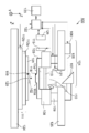
도 1은 실시 형태에 관한 임프린트 장치의 구성을 도시하는 도면이다.
도 2는 토출 수단의 구성을 도시하는 도면이다.
도 3은 제1 실시 형태에 관한 임프린트 방법을 나타내는 흐름도이다.
도 4는 기판의 표면의 높이 방향의 위치에 대하여 설명하는 도면이다.
도 5는 토출구와 기판의 거리가 일정한 경우의 임프린트재의 공급 위치를 도시하는 도면이다.
도 6은 토출구와 기판의 거리가 일정하지 않은 경우의 임프린트재의 공급 위치를 도시하는 도면이다.
도 7은 제1 실시 형태의 공급 조건의 보정 방법을 설명하는 도면이다.
도 8은 제1 실시 형태의 공급 조건의 보정 방법을 도시하는 도면이다.
도 9는 기준면에 대하여 설명하는 도면이다.
도 10은 제5 실시 형태에 관한 계측 방법을 설명하는 도면이다.
도 11은 제5 실시 형태에 관한 촬상 결과를 도시하는 도면이다.1 is a diagram showing the configuration of an imprint apparatus according to an embodiment.
2 is a view showing the configuration of the discharge means.
3 is a flowchart showing the imprint method according to the first embodiment.
It is a figure explaining the position in the height direction of the surface of a board | substrate.
5 is a view showing a supply position of the imprint material when the distance between the discharge port and the substrate is constant.
6 is a view showing a supply position of an imprint material when the distance between the discharge port and the substrate is not constant.
It is a figure explaining the correction method of the supply condition of 1st Embodiment.
8 is a diagram showing a method for correcting supply conditions in the first embodiment.
It is a figure explaining a reference plane.
It is a figure explaining the measuring method which concerns on 5th embodiment.
11 is a diagram showing imaging results according to the fifth embodiment.
[제1 실시 형태][First Embodiment]
(장치 구성)(Device configuration)
도 1은 실시 형태에 관한 임프린트 장치(100)의 구성을 도시하는 도면이다. 도 1에 있어서, 연직 방향(높이 방향)을 Z축이라 한다. 또한, 당해 Z축에 수직인 평면 내(높이 방향과 교차하는 평면 내)에서 서로 직교하는 2축을 X축 및 Y축이라 하고 있다. XY 평면 내에 있어서의 X축 방향 및 Y축 방향의 위치 성분을 (X,Y)로 나타낸다.1 is a diagram showing a configuration of an
본 실시 형태에서는 임프린트재(102)는 광 경화성 재료이다.In this embodiment, the
조사부(104)는 자외선(105)을 기판(101)에 조사하여, 미경화 상태의 임프린트재(102)를 경화시킨다. 몰드(103)의 재료는, 석영 등의 자외선(105)을 투과하는 재료이다. 조사부(104)는 자외선(105)을 출사하는 광원(106)과, 자외선(105)의 광로를 기판(101)의 방향으로 절곡하는 미러(107)를 갖는다.The
몰드(103)는 외주가 직사각형이며, 그 중심부에는 요철 패턴이 형성된 직사각형 패턴부(103a)를 갖는다. 기판(101) 상에는 패턴부(103a)와 거의 동일한 크기의 피처리 영역인 패턴 영역(120)이 복수 형성되어 있다.The
임프린트 장치(100)에서는, 임프린트재(102)와 몰드(103)를 접촉시키는 동작(이하, 압형 동작이라 함)을 행한다. 또한, 임프린트재(102)와 몰드(103)를 접촉시킨 상태에서 임프린트재(102)를 경화시킴으로써 기판(101) 상에 패턴을 형성한다.In the
기판(101)에는 복수의 패턴 영역(120)이 형성되어 있고, 임프린트 장치(100)는 1회의 압형 동작에 의해 하나의 패턴 영역(120) 상에 패턴부(103a)의 전사 패턴이 형성된다.A plurality of
하나의 패턴 영역(120)은 하나 또는 복수의 샷 영역에 상당한다. 샷 영역이란 이미 패턴 형성을 종료한 하지층의 단위 영역이며, 스크라이브 라인(도시하지 않음)에 의해 구획되어 형성되어 있다.One
하나의 샷 영역은, 예를 들어 26㎜×33㎜ 정도의 사이즈이다. 하나의 샷 영역에는 유저가 희망하는 칩 사이즈의 패턴을 하나 또는 복수 형성하는 것이 가능하다.One shot area is about 26 mm × 33 mm, for example. It is possible to form one or more patterns of a chip size desired by a user in one shot area.
척(108)은 진공 흡착력이나 정전기력에 의해 몰드(103)를 보유 지지한다. 구동 기구(109)는 척(108)과 함께 몰드(103)를 Z축 방향을 따라서 이동시킨다. 자외선(105)이 기판(101)에 도달하도록, 척(108) 및 구동 기구(109)는 중앙부에 개구 영역(110)을 갖는다. 몰드(103)의 압형 동작 및 임프린트재(102)와 몰드(103)를 분리하는 동작(이하, 이형 동작이라 함) 시에, 몰드(103)를 이동시킨다.The
임프린트 장치(100)는 기판(101)과 토출구(116a)를 상대 이동시키는 이동 수단으로서 기판 스테이지(이동 수단)(111)를 갖는다. 기판 스테이지(111)는 척(112a)과 구동 기구(112b)를 갖고, 후술하는 제어부(122)로부터의 지시에 따라서 기판(101)을 위치 결정한다. 척(112a)은 기판(101)을 진공 흡착력이나 정전기력에 의해 기판(101)을 보유 지지한다. 구동 기구(112b)는 척(112a)에 의해 기판(101)을 보유 지지한 상태에서 XY 평면 내를 따라서 이동한다. 기판(101)의 위치 계측에 사용되는 것은, 구동 기구(112b) 상에 설치되어 있다. 구동 기구(112b)는, 예를 들어 에어 실린더나 피에조 액추에이터 등이다.The
구동 기구(109) 및 구동 기구(112b)는 조동 구동계나 미동 구동계 등, 복수의 구동계로 구성되어 있어도 된다. 또한, 구동 기구(109)는 Z축 방향뿐만 아니라, X축 방향, Y축 방향 및 각 축 주위의 회전 방향으로 몰드(103)를 이동시키는 기구여도 된다. 구동 기구(112b)는 X축 방향 및 Y축 방향뿐만 아니라, 그 밖의 축 방향 및 각 축 주위의 회전 방향으로 기판(101)을 이동시키는 기구여도 된다. 압형 동작 및 이형 동작은, 몰드(103) 및 기판(101) 중 적어도 한쪽을 Z축 방향으로 이동시킴으로써 행하면 된다.The
몰드(103)의 상방에 투과 부재(113)를 배치함으로써, 개구 영역(110) 내에, 압력 조정이 가능한 공간(114)을 설치하고 있다. 임프린트재(102)에 패턴부(103a)를 접촉시킬 때, 패턴부(103a)를 기판(101)의 방향으로 볼록 형상으로 휘게 한다. 이에 의해, 몰드(103)와 임프린트재(102) 사이에 기포가 들어가는 것을 방지하고, 패턴부(103a)의 구석구석까지 임프린트재(102)를 충전시킬 수 있다.By arranging the
도 2는 토출 수단(공급 수단)(115)을 -Z 방향으로부터 본 도면이다. Y축 방향을 따라서 복수의 노즐(116)이 배열되어 있다. 토출 수단(115)은 노즐(116)의 토출구(공급구)(116a)를 포함하고, 기판 스테이지(111)가 기판(101)을 소정 방향(본 실시 형태에서는 -X 방향)으로 이동시키고 있는 동안에 토출구(116a)로부터 임프린트재(102)를 토출한다. 토출 수단(115)은 1회의 공급 동작에 의해 하나의 패턴 영역(110)분의 임프린트재(102)를 토출한다. 고정 배치된 토출 수단(115)은 임프린트재(102)를 소정의 시간 간격으로 소정량씩 토출한다. 이와 같이 하여, 기판(101) 상의 패턴 영역(120)에 임프린트재(102)를 공급한다.2 is a view of the discharge means (supply means) 115 viewed from the -Z direction. A plurality of
노즐(116)은 노즐(116)이 갖는 토출 기구로서 피에조 소자(도시하지 않음)를 갖고, 압전 효과를 이용하여 임프린트재(102)를 압출한다. 피에조 소자에 인가하는 전압의 파형(이하, 구동 파형이라 함)이나, 그 구동 파형에 따라서 전압을 인가하는 타이밍은, 후술하는 제어부(122)에 의해 지시된다. 또한, 토출 수단(115)에 의해 토출되는 임프린트재(102)는 미경화 전의 임프린트재(102)이다.The
본 실시 형태 및 후속의 실시 형태에 있어서, 토출 속도는, 임프린트재(102)가 체공 중의 속도의 적분값을, 체공 시간 Δt로 제산한 값에 상당한다. 토출 수단(115)으로부터 부여된 초속도와 공기 저항을 받아 감속되어 기판(101)에 도달하기 직전의 속도의 어긋남을 보정하고, 낙하 중인 임프린트재(102)의 속도를 등속이라고 가정하였기 때문이다.In this embodiment and the subsequent embodiments, the discharge speed corresponds to a value obtained by dividing the integral value of the speed in the body cavity by the
계측부(117)는 몰드(103)의 상방으로부터 기판(101)을 촬상하고, 패턴부(103a)에 형성되어 있는 복수의 마크(118)와 패턴 영역(120)에 형성되어 있는 복수의 마크(119)의 상대 위치의 어긋남을 계측한다.The
촬상부(121)는 몰드(103)를 투과시킨 광을 기판(101)을 향하여 조사하고, CCD 등의 촬상 소자에 의해 기판(101)으로부터의 반사광을 수광함으로써 몰드(103)와 임프린트재(102)의 접촉 상태를 촬상한다. 촬상부(121)가 촬상 기능만을 갖고 있고, 기판(101)에 조사하는 광은 촬상부(121)와는 상이한 광원(도시하지 않음)으로부터 조사해도 된다. 압인 동작 중에 있어서의 임프린트재(102)의 퍼짐을 관찰함으로써, 패턴부(103a)와 기판(101) 사이에의 파티클의 개입이나, 패턴부(103a)에의 임프린트재(102)의 충전 모습을 촬상한다.The
계측부(126)는 계측부(126)와 기판(101)의 표면의 각 위치의 거리를 계측한다. 즉, 기판(101)의 표면의 Z축 방향의 위치에 관한 정보(기판의 표면의 높이 방향의 위치에 관한 정보)를 계측한다. Z축 방향의 위치를, 이하, Z 위치라 한다. 본 실시 형태에서는, 계측부(126)는 기판(101)의 표면의 Z축 방향의 위치를 계측한다.The
계측부(126)는, 예를 들어 레이저 간섭계나, 기판에 대하여 비스듬히 광을 입사하여 반사광을 검출하는 사입사 방식의 높이 계측기 등이다. 계측부(126)는 정전 용량 센서나 인코더 등, 그 밖의 계측기여도 된다. 동시에 복수점의 계측을 할 수 있도록, 복수의 계측부를 포함하고 있어도 된다. 계측부(126)와 기판(101)의 거리는, 제어부(122)에 의한 토출구(116a)와 기판(101)의 거리의 산출에 사용된다.The
제어부(결정 수단, 보정 수단)(122)는 CPU, RAM, ROM을 갖고 있고, 조사부(104), 구동 기구(109), 기판 스테이지(111), 토출 수단(115), 계측부(117), 촬상부(121) 및 기억부(123)와 회선을 통해 접속되어 있다. 이들을 통괄적으로 제어하여, 후술하는 도 3의 흐름도에 나타내는 프로그램에 따라서 임프린트 처리를 실행한다.The control unit (determination means, correction means) 122 has a CPU, RAM, and ROM, and includes an
제어부(122)는 결정 수단으로서 기능하고, 계측부(126)의 계측 결과에 기초하여, 토출구(116a)와 기판(101)의 거리의 분포에 관한 정보를 결정한다.The
또한, 제어부(122)는 보정 수단으로서도 기능하고, 제어부(122)에 의해 결정된 토출구(116a)와 기판(101)의 거리에 관한 정보에 기초하여, 기판(101)에의 임프린트재(102)의 공급 조건을 보정한다(조정한다).In addition, the
당해 보정은, 기판(101) 상에 공급되는 임프린트재(102)의 공급 위치가 이상의 공급 위치에 근접하도록 하는 보정이다. 공급 조건은, 기판(101) 상에 임프린트재(102)가 공급되는 동안의 기판 스테이지(111)의 이동 속도, 토출구(116a)로부터의 임프린트재(102)의 토출 속도, 및 토출구(116a)로부터의 임프린트재(102)의 토출 타이밍 중 적어도 하나이다.The correction is a correction such that the supply position of the
기억부(123)는 제어부(122)에 의해 판독 가능한 하드 디스크(기억 매체) 등으로 구성된다. 도 3의 흐름도에 나타내는 프로그램, 계측부(126)와 토출 수단(115)의 각각의 Z 위치, 및 노즐(116)의 배치 등을 기억하고 있다. 베이스 정반(124)에는, 기판 스테이지(111)가 적재된다. 브리지 정반(125)에 의해, 구동 기구(109)를 현수하여 지지하고 있다.The
(임프린트 방법)(Imprint method)
본 실시 형태에 관한 임프린트 방법에 대하여 도 3에 도시하는 흐름도를 사용하여 설명한다. 또한, 본 실시 형태에 있어서 토출구(116a)와 기판(101)의 거리의 분포에 관한 정보는, 토출구(116a)와 기판(101)의 표면의 각각의 목표의 공급 위치의 높이 방향의 거리의 분포이다. 제어부(122)가 보정하는 임프린트재(102)의 공급 조건은, 기판 스테이지(111)의 속도이다. 본 실시 형태는, 임프린트재(102)를 토출 중인 기판 스테이지(111)의 이동 방향인 X축 방향으로의 공급 위치의 어긋남이, 기판 스테이지(111)의 비이동 방향인 Y축 방향으로의 공급 위치의 어긋남보다도 크게 어긋나기 쉬운 경우에 적합하다.The imprint method according to this embodiment will be described using the flowchart shown in FIG. 3. In addition, in the present embodiment, the information on the distribution of the distance between the
먼저, 계측부(126)가 기판(101)의 높이 방향의 위치를 계측한다(S101). 계측부(126)는 복수의 계측점을 대표적으로 계측한다. 그리고, 제어부(122)가 토출구(116a)와 기판(101)의 표면의 각 위치의 거리를 결정한다(S102). 제어부(122)는 계측부(126)의 계측 결과에 기초하여 토출구(116a)와 계측점 이외의 위치의 거리를 보완하는 연산 처리를 행하여, 기판(101)의 표면의 높이의 분포를 나타내는 근사 함수 F(x,y)를 구한다. 근사 함수는, F(x,y)=ax+by+f로 나타내는 1차 함수, F(x,y)=ax2+bxy+cy2+dx+ey+f로 나타내는 2차 함수, 혹은 더 고차의 함수여도 된다.First, the
계측점은 기판(101)의 중심 영역 및 외주 영역을 포함하도록 선택하는 것이 바람직하다. 중심 영역이란 기판(101)의 반경의, 절반의 반경으로 가상적으로 그려지는 원의 내측 영역이다. 외주 영역이란, 중심 영역을 둘러싸는 중심 영역보다도 외주측의 영역이다. 이에 의해 제어부(122)가 근사 함수 F(x,y)를 고정밀도로 결정할 수 있다.It is preferable to select the measurement point to include the center region and the outer circumferential region of the
계측부(126)에 의한 계측 결과에 대하여 도 4를 사용하여 설명한다. 도 4의 (a)는 기판(101)을 +Z 방향으로부터 본 도면, 도 4의 (b)는 기판(101)의 중심을 통과하는 X 위치 A-A'간의 높이 방향의 위치의 분포를 도시하는 도면이다. 하나의 패턴 영역(120) 부근의 높이 방향의 위치의 분포는, X축 방향에 대하여 1차식으로 근사된다.The measurement result by the
도 3의 흐름도의 설명으로 되돌아간다. 다음에, 제어부(122)는, 패턴 영역(120)에의 임프린트재(102)의 공급 위치가 목표의 공급 위치로 되도록 공급 조건을 보정한다(S103). 당해 공급 조건의 보정은, 기판(101) 상의 모든 패턴 영역(120)에 대하여 행한다. S103의 공정의 상세는 후술한다.Returning to the description of the flowchart in FIG. 3. Next, the
임프린트 장치(100)는 토출 수단(115) 및 기판 스테이지(111)를 사용하여, 보정 후의 공급 조건에 기초하여 패턴 영역(120)에 임프린트재(102)를 공급한다(S104). 기판 스테이지(111)는 기판(101)을 몰드(103)와 대향하는 위치로 이동시킨다. 구동 기구(109)가 몰드(103)를 하강시켜, 압형 동작을 행한다(S105).The
몰드(103)와 임프린트재(102)를 접촉시키고 있는 상태에서, 조사부(104)가 패턴 영역(120)에 자외선(105)을 조사하여, 임프린트재(102)를 경화시킨다(S106). 임프린트재(102)의 경화 후, 구동 기구(109)가 몰드(103)를 상승시켜 이형 동작을 행한다(S107).In the state in which the
다음에, 다음으로 패턴을 형성해야 할 패턴 영역(120)이 있는지를 제어부(122)가 판단한다(S108). 패턴 영역(120)이 있는 경우에는, S104 내지 S107의 공정을 반복한다. 패턴을 형성해야 할 패턴 영역(120)이 없는 경우에는, 본 프로그램을 종료하고, 복수의 패턴 영역(120)에 패턴이 형성된 기판은 임프린트 장치(100)로부터 반출된다.Next, the
또한, S103에서 하나의 패턴 영역(120)만큼의 공급 조건의 보정밖에 행하지 않은 경우에는, S108의 공정에서 "예"로 판단된 후, S103의 공정으로 되돌아간다.In addition, when only the correction of the supply condition of one
S103에 있어서의 공급 조건의 보정 방법에 대하여 설명하기 전에, 도 5의 (a) (b)에 의해 보정을 행하지 않은 경우에 대하여 설명한다.Before explaining the correction method of the supply condition in S103, the case where correction is not performed by (a) (b) of FIG. 5 is demonstrated.
도 5의 (a)는 평탄한 기판(101)의 기울기를 도시하는 도면이다. 기판(101)이 소정의 높이 H0에 있는 것을 나타내고 있다. 소정의 높이는, 기판(101)을 척(112)에 적재하였을 때의 설계의 높이이다. 도 5의 (b)는 임프린트재(102)가 공급된 패턴 영역(120)을 +Z 방향으로부터 본 도면이다.5A is a view showing the inclination of the
도 6의 (a)는 기판(101)의 표면의 기울기를 도시하는 도면이고, 도 6의 (b)는 X축 방향으로만 임프린트재(102)가 공급된 공급 위치의 어긋남이 발생한 모습을 도시하고 있다. 등간격으로 배열된 종횡의 파선의 교점(10)은 이상적인 임프린트재(102)의 공급 위치, 즉 목표 위치(목표 공급 위치)이다. 검정색 동그라미는 기판(101)에 공급된 임프린트재(102)를 나타내고 있다. 소정의 속도로 기판 스테이지(111)를 -X 방향으로 이동시키면서 임프린트재(102)를 공급하는 경우, 토출구(116a)로부터 높이 H0까지의 거리가 일정하기 때문에, 교점(10)에 임프린트재(102)가 공급된다.6 (a) is a view showing the inclination of the surface of the
도 4의 (b)에서 도시한 전술한 위치 B-B'와 같이 패턴 영역(120)의 높이 방향의 위치가 기울기를 갖는 경우, 높이 H0보다 높은 위치에서는 토출구(116a)와의 거리가 작아진다. 토출 수단(115)은 기판(101)이 X축 방향으로 이동하고 있는 동안에 임프린트재(102)를 공급한다. 따라서, 임프린트재(102)의 체공 시간이 짧아지므로, 높이 H0의 위치에 임프린트재(102)를 공급하는 경우보다도 이르게 기판(101)에 공급된다.When the position in the height direction of the
반대로, 높이 H0보다도 낮은 위치에서는 토출구(116a)와의 거리가 커진다. 따라서, 임프린트재(102)의 체공 시간은 길어지므로, 높이 H0의 위치에 임프린트재(102)를 공급하는 경우보다도 늦게 기판(101)에 공급된다.Conversely, the distance from the
따라서 도 6의 (b)에 도시한 바와 같이, 기판(101)의 높이 방향의 위치가 높이 H0으로부터 이격될수록, 교점(10)에 대한 임프린트재(102)의 위치 어긋남이 커진다.Therefore, as shown in FIG. 6 (b), the more the position in the height direction of the
기판 스테이지(111)가 이동하는 X축 방향에 대한 기판(101)의 Z축 방향의 분포에 의한 공급 위치의 어긋남에 대하여, 제어부(122)는 기판 스테이지(111)의 이동 속도를 보정하여 공급 위치의 어긋남을 보정하는 방법이다.With respect to the displacement of the supply position due to the distribution of the Z-axis direction of the
도 7은 높이 H1의 위치 A에 임프린트재(102)를 공급할 때의 모습을 도시하고 있다. 보정 전의 기판 스테이지(111)의 이동 속도를 V1이라 한다. 임프린트재(102)의 토출 속도는 V2이다. 토출구(116a)와 높이 H1의 목표 위치인 위치 A의 Z축 방향의 거리는 H1이다. 토출 시의 위치 A의 X 위치와 토출구(116a)의 X 위치의 거리가 L1일 때 토출 수단(115)은 임프린트재(102)를 토출한다. 보정 후의 기판 스테이지(111)의 이동 속도를 V1+ΔV라 할 때, 식 (1), (2)가 성립한다.7 shows a state when the
제어부(122)는 식 (1), (2)로부터 속도의 보정량 ΔV의 식 (3)을 결정한다.The
![]()
![]()
![]()
![]()
![]()
![]()
도 8의 (a)는 기판(101)의 각 X 위치의 높이와 기판 스테이지(111)의 이동 속도의 관계를 도시하고 있다.8 (a) shows the relationship between the height of each X position of the
이와 같이, 제어부(122)는 소정의 높이 H0보다도 낮은 목표 위치에 임프린트재(102)를 공급할 때의 이동 속도를 소정의 높이 H0보다도 높은 목표 위치에 임프린트재(102)를 공급할 때의 상기 이동 속도보다도 크게 한다.As described above, the
제어부(122)가 공급 조건을 보정함으로써, 토출구(116a)와 기판의 거리가 분포를 갖고 있는 경우에 있어서 종래보다도 기판(101) 상의 목표 위치에 대하여 고정밀도로 임프린트재(102)를 공급할 수 있다.The
이에 의해, 임프린트 장치(100)는 경화된 임프린트재(102)의 패턴으로서 패턴 결함이 적은 양호한 패턴을 형성할 수 있다.Thereby, the
[제2 실시 형태][Second Embodiment]
본 실시 형태에서는 계측부(126)는 기판(101)의 표면의 Z 위치를 계측한다. 본 실시 형태에 있어서 토출구(116a)와 기판(101)의 거리의 분포에 관한 정보는, 토출구(116a)와 기판(101)의 표면의 각각의 목표의 공급 위치의 높이 방향의 거리의 분포이다.In this embodiment, the
제어부(122)가 보정하는 임프린트재(102)의 공급 조건은, 임프린트재(102)의 토출 타이밍이다. 토출의 타이밍을, 1회째의 토출 개시의 시각과, 직전의 토출 시각으로부터 다음 토출 시각까지의 시간 간격(토출 간격)으로 제어하고 있는 경우의 실시 형태이다. 임프린트 장치(100)의 구성에 관하여, 설명이 없는 부분은 제1 실시 형태와 마찬가지이다.The supply condition of the
본 실시 형태는, 패턴 영역(120)에 있어서의 X축 방향으로의 기울기와 Y축 방향으로의 기울기 중 어느 쪽이 큰 경우도 적용할 수 있다. 실시 형태에 관한 임프린트 방법 중, 제1 실시 형태와는 상이한 S103의 공정만 설명한다.This embodiment can also be applied to the case where either of the inclination in the X-axis direction and the inclination in the Y-axis direction in the
토출 수단(115)이 임프린트재(102)를 토출 간격 T로 주기적으로 토출하고 있는 경우, 도 8의 (b)에 도시한 바와 같이 토출 타이밍을 제어한다. 높이가 H0보다 높은 경우에는 T에 비하여 늦게 임프린트재(102)를 토출하고, 높이가 H0보다도 낮은 경우에는 T에 비하여 이르게 임프린트재(102)를 토출한다.When the discharge means 115 periodically discharges the
즉, 높이가 소정의 높이 H0보다 낮은 목표 위치에 공급하는 임프린트재(102)의 토출 타이밍을, 소정의 높이 H0보다 높은 목표 위치에 공급하는 임프린트재(102)의 토출 타이밍보다도 이르게 한다.That is, the discharge timing of the
소정의 높이 H0보다도 높은 목표 위치에 공급하는 경우, 제어부(122)는 소정의 높이 H0에 공급하는 임프린트재(102)를 토출하고 나서 다음에 임프린트재(102)를 공급할 때까지의 시간을 T+ΔT로 하는 보정을 한다. 식 (4)에 나타내는 ΔT만큼 토출의 타이밍을 지연시킨다.When supplying to a target position higher than the predetermined height H0, the
![]()
![]()
위치 A의 다음에 공급하는 위치에 대해서는, 위치 A를 향하여 토출한 임프린트재(102)를 토출하고 나서 다음 임프린트재를 토출할 때까지의 시간을 (T+2ㆍΔT)로 하면 된다. 임프린트재(102)를 토출할 때마다 토출 타이밍을 보정함으로써, 공급 위치의 어긋남을 보정할 수 있다.For the position to be supplied next to the position A, the time from discharging the
제어부(122)가 공급 조건을 보정함으로써, 토출구(116a)와 기판의 거리가 분포를 갖고 있는 경우에 있어서 종래보다도 기판(101) 상의 목표 위치에 대하여 고정밀도로 임프린트재(102)를 공급할 수 있다.The
이에 의해, 임프린트 장치(100)는 경화된 임프린트재(102)의 패턴으로서 패턴 결함이 적은 양호한 패턴을 형성할 수 있다.Thereby, the
[제3 실시 형태][Third embodiment]
본 실시 형태에 있어서 토출구(116a)와 기판(101)의 거리의 분포에 관한 정보는, 기준 위치의 높이와 임프린트재(102)의 목표 위치의 높이의 차의 분포이다. 제어부(122)가 보정하는 임프린트재(102)의 공급 조건은, 임프린트재(102)의 토출 타이밍이다. 임프린트 장치(100)의 구성에 관하여, 설명이 없는 부분은 제1 실시 형태와 마찬가지이다. 실시 형태에 관한 임프린트 방법 중, 제1 실시 형태와는 상이한 S103의 공정만 설명한다.In this embodiment, the information regarding the distribution of the distance between the
기판(101)의 표면의 Z축 방향의 위치에 관한 정보로서, 기판(101)의 표면 형상을 계측한다. 계측부(126)는, 도 9에 도시한 바와 같은, 기판(101)의 표면 형상의 정보를 제어부(122)에 출력한다. 표면 형상은, 기판(101)의 면외 방향(본 실시 형태에서는 Z축 방향, 기판의 두께 방향)의 형상에 관한 정보이다. 계측부(126)와 기판(101)의 표면의 거리를, 기판(101) 상의 복수 개소에서 계측하고, 계측 결과에 기초하여 기판(101)의 3차원의 표면 형상을 산출한다.As information about the position of the surface of the
가상적인 평탄한 면인 기준면(201)에 대한, 기판(101)의 표면(계측 대상의 면, 몰드(103)와 대향하는 면)의 각 위치의 면외 방향으로의 어긋남에 관한 정보가 얻어진다. 기준면(201)의 중심을 기준 위치라 부른다.Information about the misalignment of the surface of the substrate 101 (the surface to be measured, the surface facing the mold 103) in the out-of-plane direction with respect to the
도 9는 기판(101)의 X축 방향의 단면도이며, 기준면(201)(파선)과 각 X 위치에서의 기판(101)의 표면의 위치(실선)의 관계를 도시하는 도면이다.9 is a cross-sectional view of the
제어부(122)는 기준 위치의 높이와 임프린트재(102)의 목표 위치의 높이의 차 ΔH의 분포를 결정한다. 도 9에서는, 목표 위치와 위치 C(X,Y)의 차 ΔH를 도시하고 있다. 토출 수단(115)으로부터의 수지의 토출 속도를 V2라 한 경우, 체공 시간이 기준 위치에 비해 ΔH/V2만큼 짧아진다.The
따라서, 토출 타이밍을 ΔT=ΔH/V2만큼 이르게 하도록, 제어부(122)는 토출 타이밍을 보정하면 된다. 제어부(122)는 다른 목표 위치에 토출하는 경우도, 마찬가지로 하여 토출 타이밍을 보정한다.Therefore, the
이와 같이 하여, 제어부(122)는 소정의 높이보다도 낮은 목표 위치에 공급하는 임프린트재(102)의 토출 타이밍을, 소정의 높이보다도 높은 목표 위치에 공급하는 임프린트재(102)의 토출 타이밍보다도 이르게 하도록 보정한다.In this way, the
제어부(122)가 공급 조건을 보정함으로써, 토출구(116a)와 기판의 거리가 분포를 갖고 있는 경우에 있어서 종래보다도 기판(101) 상의 목표 위치에 대하여 고정밀도로 임프린트재(102)를 공급할 수 있다.The
이에 의해, 임프린트 장치(100)는 경화된 임프린트재(102)의 패턴으로서 패턴 결함이 적은 양호한 패턴을 형성할 수 있다.Thereby, the
또한, 제2 실시 형태 및 제3 실시 형태에 있어서, 보정하는 토출 타이밍은 시간 간격이 아니어도 된다. 임프린트재(102)를 토출하는 타이밍을 시각으로 관리하고 있는 경우에는, 제어부(122)는 소정의 높이 H0보다도 높은 목표 위치에 공급하는 임프린트재(102)를 토출하는 시각을 보정 전의 시각보다도 이르게 한다.In addition, in 2nd Embodiment and 3rd Embodiment, the discharge timing to correct may not be a time interval. When the timing for discharging the
또한, 제어부(122)는 소정의 높이 H0보다도 낮은 목표 위치에 공급하는 임프린트재(102)를 토출하는 시각을, 보정 전의 시각보다도 늦게 하는 보정을 한다.In addition, the
이 경우, 토출 타이밍이 이르다/늦다는, 토출구(116a)의 위치(X,Y)와 목표 위치의 위치(X,Y)의 XY 평면 내에 있어서의 거리가 클 때/작을 때 토출구(116a)로부터 토출하는 것을 말한다.In this case, when the distance in the XY plane of the position (X, Y) of the
이와 같이 토출 타이밍을 보정한 경우도, 제어부(122)가 공급 조건을 보정함으로써, 기판(101) 상의 목표 위치에 대하여 고정밀도로 임프린트재(102)를 공급할 수 있다.Even when the discharge timing is corrected in this way, the
[제4 실시 형태][Fourth Embodiment]
본 실시 형태에 있어서 토출구(116a)와 기판(101)의 거리의 분포에 관한 정보는, 기준 위치의 높이와 임프린트재(102)의 목표 위치의 높이의 차의 분포이다. 기준 위치의 설명은, 제3 실시 형태와 마찬가지이기 때문에 설명을 생략한다. 제어부(122)가 보정하는 임프린트재(102)의 공급 조건은, 임프린트재(102)의 토출 속도이다. 임프린트 장치(100)의 구성에 관하여, 설명이 없는 부분은 제1 실시 형태와 마찬가지이다.In this embodiment, the information regarding the distribution of the distance between the
피에조 소자에 인가하는 전압의 구동 파형을 변경함으로써 토출 속도를 보정한다. 제어부(122)는 소정의 높이보다도 낮은 목표 위치에 공급하는 임프린트재(102)의 토출 속도를, 소정의 높이보다 높은 목표 위치에 공급하는 임프린트재(102)의 토출 속도보다도 크게 한다. 실시 형태에 관한 임프린트 방법 중, 제1 실시 형태와는 상이한 S103의 공정만 설명한다.The discharge speed is corrected by changing the driving waveform of the voltage applied to the piezo element. The
토출 속도의 보정 전에는, 기판 스테이지(111)가 +X 방향으로 속도 V1 이동하고 있는 동안에 토출 수단(115)은 임프린트재(102)를 토출 속도 V2로 토출하는 경우를 예로 들어 설명한다. 제어부(122)는 기판(101)의 목표 위치의 높이가 기준 위치의 높이 H0보다도 낮은 경우에는, 토출 속도를 V2보다도 크게 한다.Before correction of the ejection speed, the ejection means 115 ejects the
구체적으로는, 목표 위치가 높이 H0보다도 ΔH만큼 낮은 경우에는, 임프린트재(102)가 토출되고 나서 기판(101)에 공급될 때까지의 체공 시간 Δt가 Δt=(H0+ΔH)/V를 만족시키는 토출 속도 V로 보정한다.Specifically, when the target position is lower than the height H0 by ΔH, the vacancy time Δt from the
마찬가지로, 제어부(122)는 기판(101)의 목표 위치의 높이가 높이 H0보다도 높은 경우에는 토출 속도를 V2보다도 작게 한다. 구체적으로는, 목표 위치가 높이 H0보다도 ΔH만큼 높은 경우에는, Δt=(H0-ΔH)/V를 만족시키는 토출 속도 V로 보정한다.Similarly, when the height of the target position of the
이와 같이, 제어부(122)는 토출구(116a)와 기판(101)의 거리의 분포 정보에 기초하여 토출 속도를 보정한다.In this way, the
이에 의해, 목표 위치에 대한 임프린트재(102)의 공급 위치의 어긋남을 저감할 수 있다. 따라서, 임프린트 장치(100)는 경화된 임프린트재(102)의 패턴을 고정밀도로 형성할 수 있다.Thereby, the shift | offset | difference of the supply position of the
[제5 실시 형태][Fifth embodiment]
제5 실시 형태에서는, 기판(101)의 표면의 높이 방향의 위치를 계측하는 계측 수단으로서, 계측부(126) 대신에, 촬상부(121) 및 제어부(122)를 사용한다. 촬상부(121)를, 기판(101)이 이동하고 있는 동안에, 토출 수단(115)으로부터 상이한 타이밍에 토출되며 또한 기판(101)의 적어도 2개소에 공급된 임프린트재(102)를 촬상하는 촬상 수단으로서 사용한다.In the fifth embodiment, the
또한, 제어부(122)를, 촬상부(121)의 촬상 결과를 화상 처리함으로써, 당해 적어도 2개소의 위치를 산출하는 산출 수단으로서 사용한다. 임프린트 장치(100)의 구성에 관하여, 설명이 없는 부분은 제1 실시 형태와 마찬가지이다.In addition, the
이에 의해, 기판(101)의 표면의 Z 위치를 계측한다.Thereby, the Z position of the surface of the
도 10의 (a)는 토출 수단(115)과 기판 스테이지(111)를 +Z 방향으로부터 본 도면, 도 10의 (b)는 -Y 방향으로부터, 도 10의 (c)는 +X 방향으로부터 본 도면이다.Fig. 10 (a) shows the discharge means 115 and the
도 10의 (b)에 도시한 바와 같이, 기판 스테이지(111)가 기판(101)을 +X 방향으로 속도 V1으로 이동시키고 있는 동안에 토출 수단(115)은 임프린트재(102)를 토출 속도 V2로 토출한다. 기판(101)이 Y축 주위의 회전 성분 ωY 방향으로 각도 θ, X축 주위의 회전 성분 ωX 방향으로 각도 φ만큼 일방향으로 기울어져 있는 경우에 대하여 설명한다.As shown in Fig. 10B, while the
기판 스테이지(111)의 이동 방향에 대하여 수직 방향(Y축 방향)으로 거리 W만큼 이격되어 형성된 2개의 토출구(116a, 116b)를 도 10의 (c)에서 도시하고 있다.The two
각도 θ, 각도 φ를 구하는 방법에 대하여, 이하 설명한다.The method of obtaining the angle θ and the angle φ will be described below.
먼저, 기판 스테이지(111)에 기판(101)을 일정 속도 V1로 이동시키면서, 시각 T1에서, 토출 수단(115)은 토출구(116a, 116b)로부터 동시에 임프린트재(102)를 토출한다. 토출구(116a)는 먼저 임프린트재(102)를 토출하고 나서 소정 시간 T가 경과한 후(시각 T2)에 다시 한 번 임프린트재(102)를 토출한다.First, while moving the
즉 토출구(116a)는 상이한 타이밍에 기판(101)의 적어도 2개소에 토출하고 있다.That is, the
촬상부(121)는 임프린트재(102)가 공급된 기판(101)을 촬상한다. 도 11의 (a)는 촬상부(121)가 임프린트재(102)를 촬상하였을 때의 모습을 도시한다. 위치(311)는 시각 T1에 있어서 토출구(116a)로부터 토출된 임프린트재(102)의 위치이다. 위치(312)는 시각 T2에 있어서 토출구(116a)로부터 토출된 임프린트재(102)의 위치이다. 위치(313)는 시각 T1에서 토출구(116a)로부터 토출된 임프린트재(102)의 위치이다.The
다음에, 촬상부(121)가 촬상 결과를 화상 처리하여, 제어부(122)가 위치(311, 312, 313)의 위치(X,Y)를 산출한다. 제어부(122)는 산출한 위치(311, 312, 313)의 정보를 사용하여, 각도 θ, 각도 φ를 산출한다. 각도 θ, 각도 φ의 산출 방법에 대하여 도 11의 (a) 및 도 11의 (b)를 사용하여 설명한다.Next, the
위치(311)와 위치(312)의 거리는 L'이다. 거리 L'는, 시간 T 동안에 속도 V1로 기판 스테이지(111)가 진행하는 거리 L=V1ㆍT보다도 ΔL'=L'-L=L'-V1ㆍT만큼 길게 되어 있다.The distance between the
이것은, 기판(101)의 표면 형상이 수평면에 대하여 각도 θ 기울어져 있는 양만큼 착탄 위치의 높이에 거리 H의 차가 있어, 시각 T1에서 토출된 임프린트재(102)의 체공 시간 t1과, 시각 T2에서 토출된 임프린트재(102)의 체공 시간 t2가 상이한 것에 기인하고 있다.This is due to the difference in the distance H from the height of the impact position by the amount at which the surface shape of the
체공 시간의 차 ΔT=t2-t1=H/V2이기 때문에, 거리 H=(L'-V1ㆍT)ㆍV2/V1이 성립한다. 제어부(122)는 식 (10)을 계산함으로써, 각도 θ를 산출한다.Since the difference ΔT = t2-t1 = H / V2 of the flight time, the distance H = (L'-V1 · T) · V2 / V1 holds. The

제어부(122)는 얻어진 위치(311, 313)의 정보를 사용하여 각도 φ를 산출한다.The
위치(311)의 X 위치와, 위치(312)의 X 위치는 거리 D1만큼 이격되어 있다.The X position of the
이것은, 기판(101)의 표면 형상이 수평면에 대하여 각도 φ 기울어져 있는 양만큼 체공 시간이 길어지고, 체공 시간이 길어진 양만큼 기판(101)이 X축 방향으로 이동한 것에 기인하고 있다. D1/V1=Wㆍtan(φ)/V2라는 관계식이 성립한다.This is due to the fact that the surface shape of the
따라서 제어부(122)는 식 (11)을 계산함으로써 각도 φ를 산출한다.Therefore, the
![]()
![]()
이상과 같이 하여, 제어부(122)는 기판(101)의 각도 θ, 각도 φ를 산출할 수 있다.As described above, the
또한, 제어부(122)는 위치(312)와 이상적인 위치(320)의 어긋남 ΔL을 산출하여, 위치(311)의 Z 위치를 산출할 수 있다.Further, the
또한, 위치(312, 313), 각도 θ, 각도 φ를 사용하여, 위치(312, 313)의 각각의 Z 위치를 산출한다.Further, the Z positions of the
이에 의해, 위치(311, 312, 313)의, XY의 위치(높이 방향과 교차하는 평면 내에 있어서의 위치 성분)에 기초하여 기판(101)의 Z 위치를 산출한다(결정한다).Thereby, the Z position of the board |
제어부(122)는 위치(311, 312, 313)의 Z 위치에 기초하여 토출구(116a)와 기판(101)의 거리의 분포에 관한 정보를 결정하고, 임프린트재의 공급 조건을 보정한다. 상세한 보정 방법은 제1 실시 형태와 마찬가지이기 때문에, 설명을 생략한다.The
제어부(122)가 공급 조건을 보정함으로써, 토출구(116a)와 기판(101)의 거리가 분포를 갖고 있는 경우에 있어서 종래보다도 기판(101) 상의 목표 위치에 대하여 고정밀도로 임프린트재(102)를 공급할 수 있다.When the distance between the
이에 의해, 임프린트 장치(100)는 경화된 임프린트재(102)의 패턴으로서 패턴 결함이 적은 양호한 패턴을 형성할 수 있다.Thereby, the
본 실시 형태의 경우, 촬상부(121)도 제어부(122)도, 경화된 임프린트재(102)의 임프린트 처리에 사용되는 것이므로, 계측부(126)와 같은 실장의 증가를 억제할 수 있다.In the case of the present embodiment, since the
촬상부(121)를 사용하여 임프린트재(102)의 토출된 위치를 계측하기 전에, 기판(101)에 자외선(105)을 조사하여 임프린트재(102)를 경화시켜 버리는 것이 바람직하다.Before measuring the discharged position of the
제어부(122)에 의한 화상 처리 시에, 임프린트재(102)의 위치 계측의 정밀도를 향상시킬 수 있다.During the image processing by the
계측에 사용하는 기판(101)은 임프린트 처리에 사용하는 기판(프로세스 웨이퍼)과 동일해도 되고, 상이한 기판(베어 웨이퍼)을 사용해도 된다.The
프로세스 웨이퍼를 사용하는 경우에는, 임프린트재(102)가 임프린트 처리에 의해 패턴을 형성하는 영역을 피하여, 스크라이브 라인 상에 공급되도록 기판 스테이지(111)의 이동 조건이나 임프린트재(102)의 토출의 시간 간격을 조정하면 된다.When a process wafer is used, the movement conditions of the
베어 웨이퍼를 사용하는 경우에는, 임프린트재(102)의 접촉각이 커지는 재질 혹은 가공이 실시된, 계측용 전용 기판인 것이 바람직하다.In the case of using a bare wafer, it is preferable that the material for which the contact angle of the
예를 들어, 불소계 재료가 코팅된 기판을 사용하는 것이 바람직하다.For example, it is preferable to use a substrate coated with a fluorine-based material.
거리 L이 작아지도록 시간 T를 조정함으로써, 기판(101)의 복수의 영역마다의 기울기를 계측해도 된다. 제어부(122)는 복수 영역에서의 계측 결과의 보완 연산을 하여, 기판(101)의 3차원 형상을 산출해도 된다. 계측에 사용하는 토출구(116a)의 수는 2개로 한정되지 않는다. 모든 토출구를 사용하여, 기판(101)의 표면 형상을 광범위하게 계측해도 된다.By adjusting the time T so that the distance L becomes small, the inclination of each of the plurality of regions of the
또한, 예를 들어 각도 φ가 없는 것을 알고 있는 경우 등, 계측의 필요가 없는 경우에는 토출구(116a)만을 사용해도 된다.In addition, only the
[기타 실시 형태][Other embodiments]
미리 설정된 공급 조건을 제어부(122)가 보정하여 새로운 공급 조건을 작성하는 것을 중심으로 설명하였지만, 본 발명은 이것에 한정되지 않는다.Although it has been mainly described that the
예를 들어, 계측부(126) 또는 촬상부(121)를 사용하여 얻어진 토출구(116a)와 기판(101)의 거리의 분포에 관한 정보에 기초하여 공급 조건을 신규로 작성해도 된다.For example, supply conditions may be newly created based on information on the distribution of the distance between the
기판(101)과 토출구(116a)를 상대 이동시키는 이동 수단은, 노즐(116)을 이동시켜 기판(101)과 토출구(116a)를 상대 이동시켜도 된다. 임프린트 장치(100)는 토출구(116a)와 기판(101)의 거리의 분포에 관한 정보와, 제어부(122)가 보정하는 임프린트재(102)의 공급 조건과, 계측 수단으로서, 전술한 각 실시 형태에서 예로 든 것을 적절히 조합해도 된다. 조합한 실시 형태에 관한 임프린트 장치(100)라도, 기판(101) 상의 목표 위치에 대하여 고정밀도로 임프린트재(102)를 공급할 수 있다.The moving means for relatively moving the
공급 위치의 어긋남을 보정하기 위한 공급 조건으로서, 예를 들어 다음 조건을 들 수 있다. 기판(101) 상에 임프린트재(102)가 공급되는 동안의 기판 스테이지(111)의 이동 속도, 토출구(116a)로부터의 임프린트재(102)의 토출 속도, 토출구(116a)로부터의 임프린트재(102)의 토출 타이밍이다. 복수 종류의 공급 조건의 보정을 조합하여, 이들 공급 조건 중 적어도 하나의 공급 조건을 보정해도 된다.As the supply conditions for correcting the displacement of the supply position, the following conditions are exemplified. The movement speed of the
제어부(122)에 의한 공급 조건의 보정은, 복수의 토출구(116a)에 대하여 상이한 보정량을 적용해도 된다.The correction of the supply conditions by the
실시 형태에 관한 임프린트 방법으로서, 계측부(126)는 임프린트 장치(100) 외부에 배치되어 있어도 된다. 이 경우, 계측부(126)가 제어부(122)에 출력하는 정보는, 기판(101)의 표면 형상이어도 된다.As the imprint method according to the embodiment, the
제어부(122)는 임프린트 장치(100)의 다른 구성 요소와 공통의 하우징 내에 설치되어도 되고, 하우징 외에 설치되어도 된다.The
또한, 제어부(122)는 제어 대상물이나, 기능(산출 수단으로서의 기능, 결정 수단으로서의 기능, 보정 수단으로서의 기능 등)별로 상이한 제어 기판의 집합체여도 된다.Further, the
기판(101)은 유리, 세라믹스, 금속, 반도체, 임프린트재 등이 사용되고, 필요에 따라서, 그 표면에 기판과는 다른 재료의 부재가 형성되어 있어도 된다. 기판(101)은, 구체적으로는, 실리콘 웨이퍼, 화합물 반도체 웨이퍼, 석영 유리 등이다.As the
임프린트재(102)에는, 경화용 에너지가 부여됨으로써 경화되는 경화성 조성물(미경화 상태의 임프린트재라 칭하는 경우도 있음)이 사용된다.A curable composition (sometimes referred to as an uncured imprint material) that is cured by applying energy for curing is used for the
경화용 에너지로서는 전자파, 열 등이 사용된다.As the curing energy, electromagnetic waves, heat, and the like are used.
전자파로서는, 예를 들어 그 파장이 10㎚ 이상 1㎜ 이하의 범위로부터 선택되는, 적외선, 가시광선, 자외선 등의 광이다.As an electromagnetic wave, it is light, such as infrared rays, visible rays, and ultraviolet rays, whose wavelength is selected from the range of 10 nm or more and 1 mm or less, for example.
경화성 조성물은, 광의 조사에 의해, 혹은, 가열에 의해 경화되는 조성물이다. 이 중, 광에 의해 경화되는 광 경화성 조성물은, 중합성 화합물과 광 중합 개시제를 적어도 함유하고, 필요에 따라서 비중합성 화합물 또는 용제를 함유해도 된다.The curable composition is a composition that is cured by irradiation with light or by heating. Among these, the photocurable composition cured by light contains at least a polymerizable compound and a photopolymerization initiator, and may contain a non-polymerizable compound or a solvent as necessary.
비중합성 화합물은, 증감제, 수소 공여체, 내첨형 이형제, 계면 활성제, 산화 방지제, 중합체 성분 등의 군에서 선택되는 적어도 1종이다.The non-polymerizable compound is at least one selected from the group of sensitizers, hydrogen donors, internal addition type release agents, surfactants, antioxidants, and polymer components.
임프린트재(102)는 액적상, 혹은 복수의 액적이 연결되어 생긴 섬상 또는 막상으로 되어 기판(101) 상에 부여되어도 된다. 임프린트재의 점도(25℃에서의 점도)는, 예를 들어 1mPaㆍs 이상 100mPaㆍs 이하이다.The
[물품 제조에의 적용][Application to product manufacturing]
임프린트 장치(100)를 사용하여 형성한 경화물의 패턴은, 각종 물품의 적어도 일부에 항구적으로, 혹은 각종 물품을 제조할 때 일시적으로 사용된다.The pattern of the cured product formed using the
물품이란, 전기 회로 소자, 광학 소자, MEMS, 기록 소자, 센서, 혹은, 형 등이다. 전기 회로 소자로서는, DRAM, SRAM, 플래시 메모리, MRAM과 같은, 휘발성 혹은 불휘발성의 반도체 메모리나, LSI, CCD, 이미지 센서, FPGA와 같은 반도체 소자 등을 들 수 있다. 형으로서는, 임프린트용 몰드 등을 들 수 있다.The article is an electric circuit element, an optical element, a MEMS, a recording element, a sensor, or a mold. Examples of the electrical circuit elements include volatile or nonvolatile semiconductor memories such as DRAM, SRAM, flash memory, and MRAM, and semiconductor elements such as LSI, CCD, image sensor, and FPGA. Examples of the mold include a mold for imprinting and the like.
경화물의 패턴은, 상기 물품의 적어도 일부의 구성 부재로서, 그대로 사용되거나, 혹은, 레지스트 마스크로서 일시적으로 사용된다. 기판의 가공 공정에 있어서 에칭 또는 이온 주입 등이 행해진 후, 레지스트 마스크는 제거된다.The pattern of the cured product is used as it is, as a constituent member of at least a part of the article, or temporarily used as a resist mask. After etching or ion implantation or the like is performed in the substrate processing step, the resist mask is removed.
이상, 본 발명의 바람직한 실시 형태에 대하여 설명하였지만, 본 발명은 이들 실시 형태에 한정되지 않는 것은 물론이며, 그 요지의 범위 내에서 다양한 변형 및 변경이 가능하다.Although preferred embodiments of the present invention have been described above, the present invention is of course not limited to these embodiments, and various modifications and changes can be made within the scope of the gist.
본 발명은 상기 실시 형태에 제한되는 것이 아니고, 본 발명의 정신 및 범위로부터 이탈하지 않고, 다양한 변경 및 변형이 가능하다. 따라서, 본 발명의 범위를 공표하기 위해 이하의 청구항을 첨부한다.The present invention is not limited to the above embodiments, and various changes and modifications are possible without departing from the spirit and scope of the present invention. Accordingly, the following claims are appended to the disclosure of the scope of the invention.
본원은, 2015년 11월 30일에 제출된 일본 특허 출원 제2015-234318호를 기초로 하여 우선권을 주장하는 것이며, 그 기재 내용 모두를 여기에 원용한다.This application claims priority based on Japanese Patent Application No. 2015-234318, filed on November 30, 2015, and uses the entire contents herein.
100 : 임프린트 장치
101 : 기판
102 : 임프린트재
103 : 형
115 : 토출 수단(공급 수단)
116a : 토출구
122 : 제어부(결정 수단, 보정 수단)
126 : 계측부(계측 수단)100: imprint device
101: substrate
102: imprint material
103: type
115: discharge means (supply means)
116a: outlet
122: control unit (determination means, correction means)
126: measuring unit (measurement means)
Claims (13)
토출구를 포함하고, 상기 토출구로부터 상기 임프린트재를 토출하여 상기 기판에 상기 임프린트재를 공급하는 공급 수단과,
상기 기판의 표면의 높이 방향의 위치에 관한 정보를 계측하는 계측 수단과,
상기 기판과 상기 토출구를 상대 이동시키는 이동 수단을 갖고,
상기 계측 수단은, 상기 이동 수단이 상기 기판과 토출구를 상대 이동시키고 있는 동안에, 상기 토출구로부터 상이한 타이밍에 토출되고 또한 상기 기판의 적어도 2개소에 공급된 상기 임프린트재를 촬상하는 촬상 수단과, 상기 촬상 수단의 촬상 결과를 화상 처리함으로써, 상기 적어도 2개소의 상기 높이 방향과 교차하는 평면 내에 있어서의 위치 성분에 기초하여 상기 토출구와 상기 기판과 상기 적어도 2개소의 각각의 거리를 산출하는 산출 수단을 갖고,
상기 공급 수단은, 상기 산출 수단에 의해 산출된 거리에 기초하여 상기 임프린트재를 공급하는 것을 특징으로 하는 임프린트 장치.Imprint apparatus for forming a pattern of an imprint material on a substrate using a mold,
Supply means including a discharge port, and discharges the imprint material from the discharge port to supply the imprint material to the substrate,
Measuring means for measuring information regarding a position in the height direction of the surface of the substrate;
It has moving means for moving the substrate and the discharge port relative,
The measurement means comprises: imaging means for imaging the imprint material discharged at different timings from the discharge port and supplied to at least two places of the substrate while the moving means is relatively moving the substrate and the discharge port; By calculating the imaging result of the means, there is calculation means for calculating the distance between the discharge port, the substrate and the at least two locations based on the positional components in the plane intersecting the height direction of the at least two locations. ,
The supply means supplies the imprint material based on the distance calculated by the calculation means.
상기 공급 수단은, 상기 계측 수단의 계측 결과로부터 얻어진 상기 토출구와 상기 기판의 거리의 분포에 관한 정보에 기초하여 임프린트재를 공급하는 것을 특징으로 하는 임프린트 장치.According to claim 1,
The supply means supplies an imprint material based on information on the distribution of the distance between the discharge port and the substrate obtained from the measurement result of the measurement means.
상기 토출구와 상기 기판의 거리의 분포에 관한 정보에 기초하여, 상기 공급 수단의 상기 임프린트재의 공급 조건을 보정하는 보정 수단을 갖고,
상기 공급 수단은, 상기 보정 수단이 보정한 공급 조건에서 상기 임프린트재를 공급하는 것을 특징으로 하는 임프린트 장치.According to claim 1,
And correction means for correcting the supply condition of the imprint material of the supply means based on information on the distribution of the distance between the discharge port and the substrate,
The supply means supplies the imprint material under supply conditions corrected by the correction means.
상기 공급 조건은, 상기 기판의 적어도 2개소에 상기 임프린트재를 공급하는 동안의 상기 기판과 상기 토출구의 상대 이동의 속도와, 상기 토출구로부터의 상기 임프린트재의 토출 속도와, 상기 토출구로부터의 상기 임프린트재의 토출 타이밍 중 적어도 하나인 것을 특징으로 하는 임프린트 장치.According to claim 3,
The supply conditions include the speed of the relative movement of the substrate and the discharge port during the supply of the imprint material to at least two places of the substrate, the discharge speed of the imprint material from the discharge port, and the imprint material from the discharge port. Imprint apparatus, characterized in that at least one of the discharge timing.
상기 공급 조건은 상기 토출 타이밍이며, 상기 보정 수단은, 소정의 높이보다도 낮은 목표 공급 위치에 공급하는 상기 임프린트재의 토출 타이밍을, 상기 소정의 높이보다도 높은 목표 공급 위치에 공급하는 상기 임프린트재의 토출 타이밍보다도 이르게 하는 것을 특징으로 하는 임프린트 장치.According to claim 4,
The supply condition is the ejection timing, and the correction means is greater than the ejection timing of the imprint material that supplies the imprint material to a target supply position that is lower than a predetermined height, to a target supply position that is higher than the predetermined height. Imprint apparatus characterized in that it leads.
상기 공급 조건은 상기 토출 속도이며, 상기 보정 수단은, 소정의 높이보다도 낮은 목표 공급 위치에 공급하는 상기 임프린트재의 토출 속도를, 상기 소정의 높이보다 높은 목표 공급 위치에 공급하는 상기 임프린트재의 토출 속도보다도 작게 하는 것을 특징으로 하는 임프린트 장치.According to claim 4,
The supply condition is the ejection speed, and the correction means is greater than the ejection speed of the imprint material that supplies the target printing position to a target supply position lower than a predetermined height, and a target supply position higher than the predetermined height. Imprint apparatus characterized in that it is made small.
상기 공급 조건은 상기 기판과 상기 토출구의 상대 이동의 속도이며, 상기 보정 수단은, 소정의 높이보다도 낮은 목표 공급 위치에 상기 임프린트재를 공급할 때의 상기 상대 이동의 속도를 상기 소정의 높이보다도 높은 목표 공급 위치에 상기 임프린트재를 공급할 때의 상기 상대 이동의 속도보다도 크게 하는 것을 특징으로 하는 임프린트 장치.According to claim 4,
The supply condition is the speed of the relative movement of the substrate and the discharge port, and the correction means targets the speed of the relative movement when supplying the imprint material to a target supply position lower than a predetermined height higher than the predetermined height. An imprint apparatus characterized in that it is larger than the speed of the relative movement when the imprint material is supplied to the supply position.
상기 토출구와 상기 기판의 거리의 분포에 관한 정보는, 기준 위치의 높이와 상기 임프린트재의 목표 공급 위치의 높이의 차의 분포인 것을 특징으로 하는 임프린트 장치.According to claim 1,
The information on the distribution of the distance between the discharge port and the substrate is a distribution of the difference between the height of the reference position and the height of the target supply position of the imprint material.
상기 토출구와 상기 기판의 거리의 분포에 관한 정보는, 상기 토출구로부터 상기 임프린트재의 목표 공급 위치까지의 높이 방향의 거리의 분포인 것을 특징으로 하는 임프린트 장치.According to claim 1,
The information on the distribution of the distance between the discharge port and the substrate is a distribution of a distance in the height direction from the discharge port to a target supply position of the imprint material.
상기 기판의 표면의 높이 방향의 위치에 관한 정보를 계측하는 공정과,
상기 계측하는 공정에서의 계측 결과에 기초하여, 상기 높이 방향에 수직인 평면에 있어서의 임프린트재의 목표 공급 위치로부터의 어긋남이 저감되도록 임프린트재의 공급 조건을 결정하는 공정과,
상기 결정하는 공정에서 결정된 상기 공급 조건에 기초하여 상기 기판에 상기 임프린트재를 공급하는 공정을 갖고,
상기 계측하는 공정은,
상기 기판과 임프린트재를 토출하는 토출구를 상대 이동시키고 있는 동안에, 상기 토출구로부터 상이한 타이밍에 토출되고 또한 상기 기판의 적어도 2개소에 공급된 임프린트재를 촬상하는 촬상 공정과, 상기 촬상 공정의 촬상 결과를 화상 처리함으로써, 상기 토출구와 상기 적어도 2개소의 각각의 거리를 산출하는 산출 공정을 포함하고,
상기 공급 조건을 결정하는 공정은, 상기 산출 공정에서 산출된 거리에 기초하여 임프린트재의 공급 조건을 결정하는 것을 특징으로 하는 임프린트 방법.Imprint method for forming a pattern of an imprint material on a substrate using a mold,
A step of measuring information regarding a position in the height direction of the surface of the substrate,
A step of determining a supply condition of the imprint material so that the displacement from the target supply position of the imprint material in a plane perpendicular to the height direction is reduced based on the measurement result in the measuring step;
And supplying the imprint material to the substrate based on the supply conditions determined in the determining process.
The measuring process is,
While moving the substrate and the discharge port for discharging the imprint material relative to each other, an imaging process for imaging an imprint material discharged at different timings from the discharge port and supplied to at least two places of the substrate, and imaging results of the imaging process And a calculation step of calculating the distance between the discharge port and the at least two locations by performing image processing,
The step of determining the supply condition is an imprint method characterized in that the supply condition of the imprint material is determined based on the distance calculated in the calculation step.
상기 공정 후에 상기 기판을 가공하는 공정
을 포함하는 것을 특징으로 하는 물품의 제조 방법.The process of forming a pattern in a board | substrate using the imprint apparatus of any one of Claims 1-9,
Process of processing the substrate after the process
Method for producing an article comprising a.
Applications Claiming Priority (3)
| Application Number | Priority Date | Filing Date | Title |
|---|---|---|---|
| JPJP-P-2015-234318 | 2015-11-30 | ||
| JP2015234318A JP6590667B2 (en) | 2015-11-30 | 2015-11-30 | Imprint apparatus, imprint method, and article manufacturing method |
| PCT/JP2016/084601 WO2017094563A1 (en) | 2015-11-30 | 2016-11-22 | Imprinting device, imprinting method, and method for manufacturing product |
Publications (2)
| Publication Number | Publication Date |
|---|---|
| KR20180087399A KR20180087399A (en) | 2018-08-01 |
| KR102102754B1 true KR102102754B1 (en) | 2020-04-21 |
Family
ID=58797304
Family Applications (1)
| Application Number | Title | Priority Date | Filing Date |
|---|---|---|---|
| KR1020187018568A KR102102754B1 (en) | 2015-11-30 | 2016-11-22 | Imprint apparatus, imprint method and manufacturing method of article |
Country Status (4)
| Country | Link |
|---|---|
| JP (1) | JP6590667B2 (en) |
| KR (1) | KR102102754B1 (en) |
| TW (1) | TWI647089B (en) |
| WO (1) | WO2017094563A1 (en) |
Families Citing this family (3)
| Publication number | Priority date | Publication date | Assignee | Title |
|---|---|---|---|---|
| JP7015134B2 (en) * | 2017-10-12 | 2022-02-02 | キヤノン株式会社 | Imprint device, imprint method, information processing device, generation method, program and manufacturing method of goods |
| JP6988767B2 (en) * | 2018-11-07 | 2022-01-05 | オムロン株式会社 | Coating device |
| JP7257817B2 (en) * | 2019-03-04 | 2023-04-14 | キヤノン株式会社 | IMPRINT APPARATUS AND ARTICLE MANUFACTURING METHOD |
Citations (7)
| Publication number | Priority date | Publication date | Assignee | Title |
|---|---|---|---|---|
| JP2003053957A (en) * | 2001-08-20 | 2003-02-26 | Konica Corp | Ink jet recorder |
| JP2007296783A (en) | 2006-05-01 | 2007-11-15 | Canon Inc | Working device/method and device manufacturing method |
| JP4541560B2 (en) * | 1999-02-08 | 2010-09-08 | キヤノン株式会社 | Electronic device, electron source, and method of manufacturing image forming apparatus |
| JP2011128396A (en) | 2009-12-18 | 2011-06-30 | Dainippon Printing Co Ltd | Forming stamper, method of manufacturing antireflection film and antireflection film |
| JP2012069758A (en) * | 2010-09-24 | 2012-04-05 | Toshiba Corp | Drop control method and drop control device |
| JP2012190877A (en) | 2011-03-09 | 2012-10-04 | Fujifilm Corp | Nanoimprint method and nanoimprint device for use therein |
| JP2013065624A (en) | 2011-09-15 | 2013-04-11 | Fujifilm Corp | Ejection amount correction method of ink jet head, ejection amount correction device, and functional ink arrangement device and nano-imprint system |
Family Cites Families (11)
| Publication number | Priority date | Publication date | Assignee | Title |
|---|---|---|---|---|
| JPH06163499A (en) * | 1992-11-19 | 1994-06-10 | Dainippon Screen Mfg Co Ltd | Apparatus for treating wafer |
| JPH0943424A (en) * | 1995-08-01 | 1997-02-14 | Canon Inc | Production of color filter and producing device |
| JP4819577B2 (en) * | 2006-05-31 | 2011-11-24 | キヤノン株式会社 | Pattern transfer method and pattern transfer apparatus |
| JP5361309B2 (en) * | 2008-09-25 | 2013-12-04 | キヤノン株式会社 | Imprint apparatus and imprint method |
| US20100102471A1 (en) * | 2008-10-24 | 2010-04-29 | Molecular Imprints, Inc. | Fluid transport and dispensing |
| JP2011062590A (en) * | 2009-09-15 | 2011-03-31 | Seiko Epson Corp | Liquid droplet discharge method, and liquid droplet discharge device |
| JP5563319B2 (en) * | 2010-01-19 | 2014-07-30 | キヤノン株式会社 | Imprint apparatus and article manufacturing method |
| JP5335717B2 (en) * | 2010-03-16 | 2013-11-06 | 富士フイルム株式会社 | Resist composition arranging apparatus and pattern forming body manufacturing method |
| JP5214683B2 (en) * | 2010-08-31 | 2013-06-19 | 株式会社東芝 | Imprint recipe creating apparatus and method, and imprint apparatus and method |
| JP5661666B2 (en) * | 2012-02-29 | 2015-01-28 | 株式会社東芝 | Pattern forming apparatus and semiconductor device manufacturing method |
| JP6083203B2 (en) * | 2012-11-19 | 2017-02-22 | 大日本印刷株式会社 | Imprint resin dripping position determination method, imprint method, and semiconductor device manufacturing method |
-
2015
- 2015-11-30 JP JP2015234318A patent/JP6590667B2/en active Active
-
2016
- 2016-11-22 KR KR1020187018568A patent/KR102102754B1/en active IP Right Grant
- 2016-11-22 WO PCT/JP2016/084601 patent/WO2017094563A1/en active Application Filing
- 2016-11-25 TW TW105138895A patent/TWI647089B/en active
Patent Citations (7)
| Publication number | Priority date | Publication date | Assignee | Title |
|---|---|---|---|---|
| JP4541560B2 (en) * | 1999-02-08 | 2010-09-08 | キヤノン株式会社 | Electronic device, electron source, and method of manufacturing image forming apparatus |
| JP2003053957A (en) * | 2001-08-20 | 2003-02-26 | Konica Corp | Ink jet recorder |
| JP2007296783A (en) | 2006-05-01 | 2007-11-15 | Canon Inc | Working device/method and device manufacturing method |
| JP2011128396A (en) | 2009-12-18 | 2011-06-30 | Dainippon Printing Co Ltd | Forming stamper, method of manufacturing antireflection film and antireflection film |
| JP2012069758A (en) * | 2010-09-24 | 2012-04-05 | Toshiba Corp | Drop control method and drop control device |
| JP2012190877A (en) | 2011-03-09 | 2012-10-04 | Fujifilm Corp | Nanoimprint method and nanoimprint device for use therein |
| JP2013065624A (en) | 2011-09-15 | 2013-04-11 | Fujifilm Corp | Ejection amount correction method of ink jet head, ejection amount correction device, and functional ink arrangement device and nano-imprint system |
Also Published As
| Publication number | Publication date |
|---|---|
| TWI647089B (en) | 2019-01-11 |
| JP2017103313A (en) | 2017-06-08 |
| KR20180087399A (en) | 2018-08-01 |
| WO2017094563A1 (en) | 2017-06-08 |
| TW201733773A (en) | 2017-10-01 |
| JP6590667B2 (en) | 2019-10-16 |
Similar Documents
| Publication | Publication Date | Title |
|---|---|---|
| US10406743B2 (en) | Imprint apparatus, imprint method, and method of manufacturing article | |
| JP6029268B2 (en) | Imprint apparatus and article manufacturing method using the same | |
| US11413793B2 (en) | Imprint apparatus, imprint method, and method for manufacturing product | |
| KR102102754B1 (en) | Imprint apparatus, imprint method and manufacturing method of article | |
| JP6701300B2 (en) | Systems and methods for improving throughput of nanoimprint systems | |
| KR20190140397A (en) | Molding apparatus for molding composition on substrate with mold, and article manufacturing method | |
| KR102316054B1 (en) | Mould, imprint apparatus, method of manufacturing article | |
| KR20200055096A (en) | Imprint apparatus and manufacturing method of article | |
| US11526090B2 (en) | Imprint apparatus and method of manufacturing article | |
| US20210187797A1 (en) | Imprint apparatus, imprint method, and method of manufacturing article | |
| KR102382790B1 (en) | Imprint device, imprint method, information processing device, generating method, program, and method of manufacturing article | |
| JP6548560B2 (en) | IMPRINT APPARATUS, MEASUREMENT METHOD, IMPRINT METHOD, AND ARTICLE MANUFACTURING METHOD | |
| TWI631599B (en) | Imprinting apparatus, measurement method, imprinting method, and article manufacturing method | |
| JP6552392B2 (en) | Imprint apparatus, measurement method, imprint method, and article manufacturing method | |
| US11573487B2 (en) | Imprint apparatus, imprinting method, and method of manufacturing article | |
| JP7441037B2 (en) | Imprint device, information processing device, imprint method, and article manufacturing method | |
| US11664225B2 (en) | Imprint apparatus, and product manufacturing method | |
| KR20190133600A (en) | Data generation method, imprint method, imprint apparatus, and method of manufacturing article | |
| JP7289895B2 (en) | IMPRINT APPARATUS, IMPRINT METHOD, AND ARTICLE MANUFACTURING METHOD | |
| US20230182356A1 (en) | Imprint apparatus and article manufacturing method | |
| JP2022190891A (en) | Liquid discharge device, liquid discharge method, molding device, and manufacturing method for article | |
| KR20230040894A (en) | Liquid discharge apparatus, liquid discharge method, film forming apparatus, and article manufacturing method | |
| KR20230068314A (en) | Imprint apparatus and article manufacturing method | |
| JP2023020142A (en) | Liquid dispensing device, liquid dispensing method, molding device, and method for manufacturing article | |
| JP2019079877A (en) | Imprint apparatus, article manufacturing method, determination method, information processing apparatus, and program |
Legal Events
| Date | Code | Title | Description |
|---|---|---|---|
| A201 | Request for examination | ||
| E902 | Notification of reason for refusal | ||
| E90F | Notification of reason for final refusal | ||
| E701 | Decision to grant or registration of patent right | ||
| GRNT | Written decision to grant |