KR101995309B1 - Polarizing lighting systems - Google Patents
Polarizing lighting systems Download PDFInfo
- Publication number
- KR101995309B1 KR101995309B1 KR1020137010519A KR20137010519A KR101995309B1 KR 101995309 B1 KR101995309 B1 KR 101995309B1 KR 1020137010519 A KR1020137010519 A KR 1020137010519A KR 20137010519 A KR20137010519 A KR 20137010519A KR 101995309 B1 KR101995309 B1 KR 101995309B1
- Authority
- KR
- South Korea
- Prior art keywords
- light
- optically active
- nanorods
- active structure
- emitted
- Prior art date
Links
- 239000002073 nanorod Substances 0.000 claims abstract description 261
- 238000005086 pumping Methods 0.000 claims abstract description 80
- 230000004044 response Effects 0.000 claims abstract description 13
- 230000010287 polarization Effects 0.000 claims description 68
- 238000005286 illumination Methods 0.000 claims description 45
- 230000003287 optical effect Effects 0.000 claims description 44
- 239000000463 material Substances 0.000 claims description 17
- 239000000758 substrate Substances 0.000 claims description 17
- 239000004065 semiconductor Substances 0.000 claims description 12
- 238000000034 method Methods 0.000 claims description 10
- 238000000605 extraction Methods 0.000 claims description 8
- 239000011258 core-shell material Substances 0.000 claims 1
- 239000010410 layer Substances 0.000 description 66
- 239000010408 film Substances 0.000 description 38
- 239000002105 nanoparticle Substances 0.000 description 36
- 229920000642 polymer Polymers 0.000 description 23
- 101150059062 apln gene Proteins 0.000 description 20
- 239000003086 colorant Substances 0.000 description 17
- 230000005284 excitation Effects 0.000 description 13
- 239000000203 mixture Substances 0.000 description 12
- UHYPYGJEEGLRJD-UHFFFAOYSA-N cadmium(2+);selenium(2-) Chemical compound [Se-2].[Cd+2] UHYPYGJEEGLRJD-UHFFFAOYSA-N 0.000 description 10
- 239000011521 glass Substances 0.000 description 10
- 238000013459 approach Methods 0.000 description 8
- 230000000694 effects Effects 0.000 description 7
- 230000005540 biological transmission Effects 0.000 description 6
- 239000004973 liquid crystal related substance Substances 0.000 description 6
- 239000011159 matrix material Substances 0.000 description 6
- 229920006254 polymer film Polymers 0.000 description 6
- 239000002245 particle Substances 0.000 description 5
- -1 HgSe Inorganic materials 0.000 description 4
- 238000010521 absorption reaction Methods 0.000 description 4
- 238000006243 chemical reaction Methods 0.000 description 4
- 238000013461 design Methods 0.000 description 4
- 230000005684 electric field Effects 0.000 description 4
- 230000001965 increasing effect Effects 0.000 description 4
- 239000003446 ligand Substances 0.000 description 4
- 229920002037 poly(vinyl butyral) polymer Polymers 0.000 description 4
- 238000004064 recycling Methods 0.000 description 4
- 239000002356 single layer Substances 0.000 description 4
- YXFVVABEGXRONW-UHFFFAOYSA-N Toluene Chemical compound CC1=CC=CC=C1 YXFVVABEGXRONW-UHFFFAOYSA-N 0.000 description 3
- 230000008901 benefit Effects 0.000 description 3
- 238000005538 encapsulation Methods 0.000 description 3
- 238000004020 luminiscence type Methods 0.000 description 3
- 230000001902 propagating effect Effects 0.000 description 3
- 238000004088 simulation Methods 0.000 description 3
- FJLUATLTXUNBOT-UHFFFAOYSA-N 1-Hexadecylamine Chemical compound CCCCCCCCCCCCCCCCN FJLUATLTXUNBOT-UHFFFAOYSA-N 0.000 description 2
- PMBXCGGQNSVESQ-UHFFFAOYSA-N 1-Hexanethiol Chemical compound CCCCCCS PMBXCGGQNSVESQ-UHFFFAOYSA-N 0.000 description 2
- 239000004593 Epoxy Substances 0.000 description 2
- 229910001218 Gallium arsenide Inorganic materials 0.000 description 2
- REYJJPSVUYRZGE-UHFFFAOYSA-N Octadecylamine Chemical compound CCCCCCCCCCCCCCCCCCN REYJJPSVUYRZGE-UHFFFAOYSA-N 0.000 description 2
- 229920002125 Sokalan® Polymers 0.000 description 2
- PLZVEHJLHYMBBY-UHFFFAOYSA-N Tetradecylamine Chemical compound CCCCCCCCCCCCCCN PLZVEHJLHYMBBY-UHFFFAOYSA-N 0.000 description 2
- 239000002253 acid Substances 0.000 description 2
- 238000004458 analytical method Methods 0.000 description 2
- 230000009286 beneficial effect Effects 0.000 description 2
- 230000015572 biosynthetic process Effects 0.000 description 2
- 230000000903 blocking effect Effects 0.000 description 2
- 230000008859 change Effects 0.000 description 2
- JRBPAEWTRLWTQC-UHFFFAOYSA-N dodecylamine Chemical compound CCCCCCCCCCCCN JRBPAEWTRLWTQC-UHFFFAOYSA-N 0.000 description 2
- SVMUEEINWGBIPD-UHFFFAOYSA-N dodecylphosphonic acid Chemical compound CCCCCCCCCCCCP(O)(O)=O SVMUEEINWGBIPD-UHFFFAOYSA-N 0.000 description 2
- 229920002313 fluoropolymer Polymers 0.000 description 2
- GJWAEWLHSDGBGG-UHFFFAOYSA-N hexylphosphonic acid Chemical compound CCCCCCP(O)(O)=O GJWAEWLHSDGBGG-UHFFFAOYSA-N 0.000 description 2
- 238000005259 measurement Methods 0.000 description 2
- 229910052751 metal Inorganic materials 0.000 description 2
- 239000002184 metal Substances 0.000 description 2
- 239000000178 monomer Substances 0.000 description 2
- 239000002159 nanocrystal Substances 0.000 description 2
- 239000002070 nanowire Substances 0.000 description 2
- 229920003229 poly(methyl methacrylate) Polymers 0.000 description 2
- 239000004584 polyacrylic acid Substances 0.000 description 2
- 239000004926 polymethyl methacrylate Substances 0.000 description 2
- 238000001228 spectrum Methods 0.000 description 2
- 238000003786 synthesis reaction Methods 0.000 description 2
- 238000002834 transmittance Methods 0.000 description 2
- TUQOTMZNTHZOKS-UHFFFAOYSA-N tributylphosphine Chemical compound CCCCP(CCCC)CCCC TUQOTMZNTHZOKS-UHFFFAOYSA-N 0.000 description 2
- KREGXBHGJXTOKZ-UHFFFAOYSA-N tridecylphosphonic acid Chemical compound CCCCCCCCCCCCCP(O)(O)=O KREGXBHGJXTOKZ-UHFFFAOYSA-N 0.000 description 2
- RMZAYIKUYWXQPB-UHFFFAOYSA-N trioctylphosphane Chemical compound CCCCCCCCP(CCCCCCCC)CCCCCCCC RMZAYIKUYWXQPB-UHFFFAOYSA-N 0.000 description 2
- ZMBHCYHQLYEYDV-UHFFFAOYSA-N trioctylphosphine oxide Chemical compound CCCCCCCCP(=O)(CCCCCCCC)CCCCCCCC ZMBHCYHQLYEYDV-UHFFFAOYSA-N 0.000 description 2
- 229920002554 vinyl polymer Polymers 0.000 description 2
- DKIDEFUBRARXTE-UHFFFAOYSA-N 3-mercaptopropanoic acid Chemical compound OC(=O)CCS DKIDEFUBRARXTE-UHFFFAOYSA-N 0.000 description 1
- 229910017115 AlSb Inorganic materials 0.000 description 1
- 229910004613 CdTe Inorganic materials 0.000 description 1
- 229910005540 GaP Inorganic materials 0.000 description 1
- 229910005542 GaSb Inorganic materials 0.000 description 1
- 229910004262 HgTe Inorganic materials 0.000 description 1
- 229910000673 Indium arsenide Inorganic materials 0.000 description 1
- GPXJNWSHGFTCBW-UHFFFAOYSA-N Indium phosphide Chemical compound [In]#P GPXJNWSHGFTCBW-UHFFFAOYSA-N 0.000 description 1
- 240000002329 Inga feuillei Species 0.000 description 1
- 239000005062 Polybutadiene Substances 0.000 description 1
- 239000004698 Polyethylene Substances 0.000 description 1
- 229920002367 Polyisobutene Polymers 0.000 description 1
- 239000004743 Polypropylene Substances 0.000 description 1
- 239000004793 Polystyrene Substances 0.000 description 1
- 239000004372 Polyvinyl alcohol Substances 0.000 description 1
- 241001455273 Tetrapoda Species 0.000 description 1
- 229910010413 TiO 2 Inorganic materials 0.000 description 1
- 229910007709 ZnTe Inorganic materials 0.000 description 1
- 230000002730 additional effect Effects 0.000 description 1
- 229910045601 alloy Inorganic materials 0.000 description 1
- 239000000956 alloy Substances 0.000 description 1
- 229910052782 aluminium Inorganic materials 0.000 description 1
- XAGFODPZIPBFFR-UHFFFAOYSA-N aluminium Chemical compound [Al] XAGFODPZIPBFFR-UHFFFAOYSA-N 0.000 description 1
- 150000001412 amines Chemical class 0.000 description 1
- 238000000149 argon plasma sintering Methods 0.000 description 1
- HDFRDWFLWVCOGP-UHFFFAOYSA-N carbonothioic O,S-acid Chemical class OC(S)=O HDFRDWFLWVCOGP-UHFFFAOYSA-N 0.000 description 1
- 229910052956 cinnabar Inorganic materials 0.000 description 1
- 239000000084 colloidal system Substances 0.000 description 1
- 238000004891 communication Methods 0.000 description 1
- 238000009833 condensation Methods 0.000 description 1
- 230000005494 condensation Effects 0.000 description 1
- 238000010276 construction Methods 0.000 description 1
- 229910052802 copper Inorganic materials 0.000 description 1
- 230000008878 coupling Effects 0.000 description 1
- 238000010168 coupling process Methods 0.000 description 1
- 238000005859 coupling reaction Methods 0.000 description 1
- 230000003247 decreasing effect Effects 0.000 description 1
- 230000001419 dependent effect Effects 0.000 description 1
- 230000008021 deposition Effects 0.000 description 1
- 239000004205 dimethyl polysiloxane Substances 0.000 description 1
- 239000006185 dispersion Substances 0.000 description 1
- 238000001035 drying Methods 0.000 description 1
- 230000009977 dual effect Effects 0.000 description 1
- 230000005611 electricity Effects 0.000 description 1
- 238000005516 engineering process Methods 0.000 description 1
- 230000002708 enhancing effect Effects 0.000 description 1
- 125000003700 epoxy group Chemical group 0.000 description 1
- 239000004744 fabric Substances 0.000 description 1
- 238000009501 film coating Methods 0.000 description 1
- 238000009472 formulation Methods 0.000 description 1
- ORTRWBYBJVGVQC-UHFFFAOYSA-N hexadecane-1-thiol Chemical compound CCCCCCCCCCCCCCCCS ORTRWBYBJVGVQC-UHFFFAOYSA-N 0.000 description 1
- WPYVAWXEWQSOGY-UHFFFAOYSA-N indium antimonide Chemical compound [Sb]#[In] WPYVAWXEWQSOGY-UHFFFAOYSA-N 0.000 description 1
- RPQDHPTXJYYUPQ-UHFFFAOYSA-N indium arsenide Chemical compound [In]#[As] RPQDHPTXJYYUPQ-UHFFFAOYSA-N 0.000 description 1
- 238000007689 inspection Methods 0.000 description 1
- 239000007788 liquid Substances 0.000 description 1
- 238000005272 metallurgy Methods 0.000 description 1
- 239000002086 nanomaterial Substances 0.000 description 1
- 239000013307 optical fiber Substances 0.000 description 1
- MPQXHAGKBWFSNV-UHFFFAOYSA-N oxidophosphanium Chemical class [PH3]=O MPQXHAGKBWFSNV-UHFFFAOYSA-N 0.000 description 1
- 150000003003 phosphines Chemical class 0.000 description 1
- 150000003009 phosphonic acids Chemical class 0.000 description 1
- 229920000435 poly(dimethylsiloxane) Polymers 0.000 description 1
- 229920002239 polyacrylonitrile Polymers 0.000 description 1
- 229920000767 polyaniline Polymers 0.000 description 1
- 229920002857 polybutadiene Polymers 0.000 description 1
- 229920000647 polyepoxide Polymers 0.000 description 1
- 229920000573 polyethylene Polymers 0.000 description 1
- 229920001155 polypropylene Polymers 0.000 description 1
- 229920001296 polysiloxane Polymers 0.000 description 1
- 229920002223 polystyrene Polymers 0.000 description 1
- 229920002451 polyvinyl alcohol Polymers 0.000 description 1
- 239000002243 precursor Substances 0.000 description 1
- 238000004321 preservation Methods 0.000 description 1
- 230000008569 process Effects 0.000 description 1
- 230000000644 propagated effect Effects 0.000 description 1
- 239000002096 quantum dot Substances 0.000 description 1
- 238000006862 quantum yield reaction Methods 0.000 description 1
- SBIBMFFZSBJNJF-UHFFFAOYSA-N selenium;zinc Chemical compound [Se]=[Zn] SBIBMFFZSBJNJF-UHFFFAOYSA-N 0.000 description 1
- 239000010703 silicon Substances 0.000 description 1
- 229910052710 silicon Inorganic materials 0.000 description 1
- 229920005573 silicon-containing polymer Polymers 0.000 description 1
- 238000003980 solgel method Methods 0.000 description 1
- 239000007787 solid Substances 0.000 description 1
- 239000000126 substance Substances 0.000 description 1
- 239000010409 thin film Substances 0.000 description 1
- 150000003573 thiols Chemical class 0.000 description 1
- 238000011144 upstream manufacturing Methods 0.000 description 1
- XLOMVQKBTHCTTD-UHFFFAOYSA-N zinc oxide Inorganic materials [Zn]=O XLOMVQKBTHCTTD-UHFFFAOYSA-N 0.000 description 1
Images


Classifications
-
- G—PHYSICS
- G02—OPTICS
- G02F—OPTICAL DEVICES OR ARRANGEMENTS FOR THE CONTROL OF LIGHT BY MODIFICATION OF THE OPTICAL PROPERTIES OF THE MEDIA OF THE ELEMENTS INVOLVED THEREIN; NON-LINEAR OPTICS; FREQUENCY-CHANGING OF LIGHT; OPTICAL LOGIC ELEMENTS; OPTICAL ANALOGUE/DIGITAL CONVERTERS
- G02F1/00—Devices or arrangements for the control of the intensity, colour, phase, polarisation or direction of light arriving from an independent light source, e.g. switching, gating or modulating; Non-linear optics
- G02F1/01—Devices or arrangements for the control of the intensity, colour, phase, polarisation or direction of light arriving from an independent light source, e.g. switching, gating or modulating; Non-linear optics for the control of the intensity, phase, polarisation or colour
- G02F1/13—Devices or arrangements for the control of the intensity, colour, phase, polarisation or direction of light arriving from an independent light source, e.g. switching, gating or modulating; Non-linear optics for the control of the intensity, phase, polarisation or colour based on liquid crystals, e.g. single liquid crystal display cells
- G02F1/133—Constructional arrangements; Operation of liquid crystal cells; Circuit arrangements
- G02F1/1333—Constructional arrangements; Manufacturing methods
- G02F1/1335—Structural association of cells with optical devices, e.g. polarisers or reflectors
- G02F1/1336—Illuminating devices
- G02F1/133617—Illumination with ultraviolet light; Luminescent elements or materials associated to the cell
-
- G—PHYSICS
- G02—OPTICS
- G02F—OPTICAL DEVICES OR ARRANGEMENTS FOR THE CONTROL OF LIGHT BY MODIFICATION OF THE OPTICAL PROPERTIES OF THE MEDIA OF THE ELEMENTS INVOLVED THEREIN; NON-LINEAR OPTICS; FREQUENCY-CHANGING OF LIGHT; OPTICAL LOGIC ELEMENTS; OPTICAL ANALOGUE/DIGITAL CONVERTERS
- G02F1/00—Devices or arrangements for the control of the intensity, colour, phase, polarisation or direction of light arriving from an independent light source, e.g. switching, gating or modulating; Non-linear optics
- G02F1/01—Devices or arrangements for the control of the intensity, colour, phase, polarisation or direction of light arriving from an independent light source, e.g. switching, gating or modulating; Non-linear optics for the control of the intensity, phase, polarisation or colour
- G02F1/13—Devices or arrangements for the control of the intensity, colour, phase, polarisation or direction of light arriving from an independent light source, e.g. switching, gating or modulating; Non-linear optics for the control of the intensity, phase, polarisation or colour based on liquid crystals, e.g. single liquid crystal display cells
- G02F1/133—Constructional arrangements; Operation of liquid crystal cells; Circuit arrangements
- G02F1/1333—Constructional arrangements; Manufacturing methods
- G02F1/1335—Structural association of cells with optical devices, e.g. polarisers or reflectors
- G02F1/1336—Illuminating devices
- G02F1/13362—Illuminating devices providing polarized light, e.g. by converting a polarisation component into another one
-
- G—PHYSICS
- G02—OPTICS
- G02F—OPTICAL DEVICES OR ARRANGEMENTS FOR THE CONTROL OF LIGHT BY MODIFICATION OF THE OPTICAL PROPERTIES OF THE MEDIA OF THE ELEMENTS INVOLVED THEREIN; NON-LINEAR OPTICS; FREQUENCY-CHANGING OF LIGHT; OPTICAL LOGIC ELEMENTS; OPTICAL ANALOGUE/DIGITAL CONVERTERS
- G02F1/00—Devices or arrangements for the control of the intensity, colour, phase, polarisation or direction of light arriving from an independent light source, e.g. switching, gating or modulating; Non-linear optics
- G02F1/01—Devices or arrangements for the control of the intensity, colour, phase, polarisation or direction of light arriving from an independent light source, e.g. switching, gating or modulating; Non-linear optics for the control of the intensity, phase, polarisation or colour
- G02F1/13—Devices or arrangements for the control of the intensity, colour, phase, polarisation or direction of light arriving from an independent light source, e.g. switching, gating or modulating; Non-linear optics for the control of the intensity, phase, polarisation or colour based on liquid crystals, e.g. single liquid crystal display cells
- G02F1/133—Constructional arrangements; Operation of liquid crystal cells; Circuit arrangements
- G02F1/1333—Constructional arrangements; Manufacturing methods
- G02F1/1335—Structural association of cells with optical devices, e.g. polarisers or reflectors
- G02F1/1336—Illuminating devices
- G02F1/133614—Illuminating devices using photoluminescence, e.g. phosphors illuminated by UV or blue light
-
- G—PHYSICS
- G02—OPTICS
- G02F—OPTICAL DEVICES OR ARRANGEMENTS FOR THE CONTROL OF LIGHT BY MODIFICATION OF THE OPTICAL PROPERTIES OF THE MEDIA OF THE ELEMENTS INVOLVED THEREIN; NON-LINEAR OPTICS; FREQUENCY-CHANGING OF LIGHT; OPTICAL LOGIC ELEMENTS; OPTICAL ANALOGUE/DIGITAL CONVERTERS
- G02F1/00—Devices or arrangements for the control of the intensity, colour, phase, polarisation or direction of light arriving from an independent light source, e.g. switching, gating or modulating; Non-linear optics
- G02F1/01—Devices or arrangements for the control of the intensity, colour, phase, polarisation or direction of light arriving from an independent light source, e.g. switching, gating or modulating; Non-linear optics for the control of the intensity, phase, polarisation or colour
- G02F1/13—Devices or arrangements for the control of the intensity, colour, phase, polarisation or direction of light arriving from an independent light source, e.g. switching, gating or modulating; Non-linear optics for the control of the intensity, phase, polarisation or colour based on liquid crystals, e.g. single liquid crystal display cells
- G02F1/133—Constructional arrangements; Operation of liquid crystal cells; Circuit arrangements
- G02F1/1333—Constructional arrangements; Manufacturing methods
- G02F1/1335—Structural association of cells with optical devices, e.g. polarisers or reflectors
- G02F1/1336—Illuminating devices
- G02F1/133621—Illuminating devices providing coloured light
-
- G—PHYSICS
- G02—OPTICS
- G02F—OPTICAL DEVICES OR ARRANGEMENTS FOR THE CONTROL OF LIGHT BY MODIFICATION OF THE OPTICAL PROPERTIES OF THE MEDIA OF THE ELEMENTS INVOLVED THEREIN; NON-LINEAR OPTICS; FREQUENCY-CHANGING OF LIGHT; OPTICAL LOGIC ELEMENTS; OPTICAL ANALOGUE/DIGITAL CONVERTERS
- G02F2202/00—Materials and properties
- G02F2202/36—Micro- or nanomaterials
-
- G—PHYSICS
- G02—OPTICS
- G02F—OPTICAL DEVICES OR ARRANGEMENTS FOR THE CONTROL OF LIGHT BY MODIFICATION OF THE OPTICAL PROPERTIES OF THE MEDIA OF THE ELEMENTS INVOLVED THEREIN; NON-LINEAR OPTICS; FREQUENCY-CHANGING OF LIGHT; OPTICAL LOGIC ELEMENTS; OPTICAL ANALOGUE/DIGITAL CONVERTERS
- G02F2203/00—Function characteristic
- G02F2203/34—Colour display without the use of colour mosaic filters
Landscapes
- Physics & Mathematics (AREA)
- Nonlinear Science (AREA)
- Mathematical Physics (AREA)
- Chemical & Material Sciences (AREA)
- Crystallography & Structural Chemistry (AREA)
- General Physics & Mathematics (AREA)
- Optics & Photonics (AREA)
- Planar Illumination Modules (AREA)
- Liquid Crystal (AREA)
- Polarising Elements (AREA)
- Light Guides In General And Applications Therefor (AREA)
Abstract
광학활성 나노로드(104A, 104B)의 적어도 2개의 상이한 그룹(G1, G2)를 포함하는 광학활성 구조(100)가 제공된다. 나노로드의 그룹은 펌핑 광에 응답하여 발광된 광의 파장 및 편관중 적어도 하나에서 서로 상이하다. 동일한 그룹의 나노로드는 적어도 하나의 다른 그룹의 나노로드의 정렬축에 실질상 평행하거나 수직인 특정 정렬축과 균일하게 정렬되어서, 상기 적어도 2개의 상이한 그룹의 나노로드는 하나 또는 2개의 정렬축을 갖고 있다. 광학활성 구조는 디스플레이용 컬러 편광 광원으로서 사용된다. There is provided an optically active structure 100 comprising at least two different groups G1, G2 of optically active nanorods 104A, 104B. The group of the nano-rods are different from each other in at least one of the wavelength and the lumen of the light emitted in response to the pumping light. Wherein the nanorods of the same group are uniformly aligned with a specific alignment axis substantially parallel or perpendicular to the alignment axis of at least one other group of nanorods such that the at least two different groups of nanorods have one or two alignment axes have. The optically active structure is used as a color polarized light source for a display.
Description
본 발명은 일반적으로 편광 조명 시스템의 분야에 관한 것이고, 특히 디스플레이용 백라이트 시스템으로서 사용되는 광학 펌핑되는 편광 조명 시스템에 관한 것이다. The present invention relates generally to the field of polarized illumination systems, and more particularly to optically pumped polarized illumination systems for use as backlight systems for displays.
광의 편광 특성은 평판 액정 디스플레이(LCD)로부터 현미경, 금속야금 검사 및 광 통신에 이르는 다양한 광학적 애플리케이션(제품 및 방법)에서 사용된다. 대부분의 광원에 의해 생성된 광은 특정 편광을 갖고 있지 않고, 전형적인 편광 선택된 다양한 타입의 편광기를 사용하여 이루어지고 있다. 편광기를 사용한 특정 편광의 선택은 에너지 손실을 통해 이루어지고, 충돌 광의 약 50%가 비편광된 광원을 사용하여 편광된 조명을 제공하기 위해 단순한 수동형 (비발광) 편광기를 사용할 때 손실될 수 있다. 이러한 문제는 에너지 절감이 중요한 요인이 되는 LCD 디스플레이용 백라이트 시스템에서 특히 크다. 이러한 문제는 배터리 수명이 중요한 문제가 되는 모바일 장치(랩톱, 휴대폰, 카메라등)에서 더 크다. The polarization properties of light are used in a variety of optical applications (products and methods) ranging from flat panel liquid crystal displays (LCDs) to microscopes, metal metallurgy inspection and optical communications. The light generated by most light sources does not have a particular polarization, but is done using various types of polarisers of typical polarization. Selection of specific polarizations with polarizers is done through energy loss and about 50% of the impinging light can be lost when using a simple passive (non-luminous) polarizer to provide polarized illumination using unpolarized light sources. This problem is particularly large in backlight systems for LCD displays, where energy savings are an important factor. These problems are greater in mobile devices (laptop, cell phone, camera, etc.) where battery life is a critical issue.
비편광된 광원에 의해 발광된 광의 비교적 효율적인 편광 선택은 발광된 광의 광경로에 특별한 표면을 갖는 복잡하고 수동형의(비발광) 중합체 필름을 위치시킴으로써 달성될 수 있다. 이러한 필름은 광의 일부를 재활용할 수 있고, 따라서 요구되는 편광의 광의 전송율을 높인다. 광의 재활용은 반사면으로의 원치않는 편광의 반사 광 성분에 기초하고 있어서, 연속 반사 후에 편광 해소하는 증대된 반사된 광 성분을 생성하고, 따라서, 적어도 일부 광 성분은 각 반사 후에 전송된다. 그러나, 이러한 수동형 시스템은 증가된 (심지어 수십개의) 층이 효율적인 재활용을 위해 필요하기 때문에 생산 비용이 높고 복잡하다. 편광기를 통해 백라이트 출력을 재활용하는 다른 "수동형" 접근법은 반사형 나노와이어 그리드 편광기(Ge, Zhibing and Wu, Shin-Tson. "Nanowire grid polarizer for energy efficient and wide-view liquid crystal displays.", Applied Physics Letters, 93, 121104, 2008)를 사용한다. The relatively efficient polarization selection of the light emitted by the unpolarized light source can be achieved by placing a complex, passive (non-luminescent) polymer film having a specific surface in the light path of the emitted light. Such a film can recycle part of the light, thus increasing the transmission rate of the required polarized light. Recycling of light is based on the reflected light component of undesired polarization to the reflective surface, producing an increased reflected light component that depolarizes after continuous reflection, and thus at least some light components are transmitted after each reflection. However, these passive systems are expensive and complex to produce because increased (even dozens of) layers are required for efficient recycling. Another "passive" approach to recycling the backlight output through a polarizer is to use a reflective nanowire grid polarizer (Ge, Zhibing and Wu, Shin-Tson. "Nanowire grid polarizer for energy efficient and wide- Letters, 93, 121104, 2008).
상술된 바와 같은 수동형 접근법은 백라이트 시스템의 설계를 복잡하게 하고 비용이 크다. 또한 이러한 접근법은 발광된 광의 색역의 품질을 강화하는데 도움이 되지 않는데, 그 이유는 파장 종속되어 있기 때문이다. 사실, 오리지널 백라이트의 색역을 보존할 필요는 백라이트 시스템의 층 구조를 더 복잡하게 한다. The passive approach as described above complicates the design of the backlight system and is costly. This approach also does not help enhance the quality of the gamut of the emitted light, because it is wavelength dependent. In fact, the need to preserve the gamut of the original backlight further complicates the layer structure of the backlight system.
나노로드(nanorod)(또한, 때로 "로드(rod)"로도 불린다)와 같은 이방성 (긴) 나노입자가 편광된 광선을 제공할 수 있는 것으로 알려져 있다. 이것은 또한, 본 출원의 양수인에게 양도된 WO 2010/095140에 기술되어 있다. It is known that anisotropic (long) nanoparticles such as nanorods (also sometimes referred to as "rods") can provide polarized light. This is also described in WO 2010/095140, assigned to the assignee of the present application.
편광된 광선을 제공하는 일부 나노로드 시스템은 다음의 발행물에 기술되어 있다. Some nanorod systems that provide polarized light are described in the following publications.
X. Peng et al., "Shape control of CdSe nanocrystals", Nature 404, 59-61, 2000은 중합체에 매입된 반도체 코어 (셀 없음) CdSe 나노로드에 기초한 콜로이드를 기술하고 있다. 거의 온전한 편광이 단일 로드로부터 얻어질 수 있다. X. Peng et al., "Shape control of CdSe nanocrystals ", Nature 404, 59-61, 2000 describe colloids based on CdSe nanorods embedded in polymer-embedded semiconductor cores (no cells). Almost intact polarized light can be obtained from a single rod.
T. Mokari and U. Banin, "Synthesis and properties of CdSe/ZnS rod/shell nanocrystals", Chemistry of Materials 15(20), 3955-3960, 2003은 로드 구조에 셀을 성장시킴으로써 강화되는 로드의 발광을 설명하고 있다. T. Mokari and U. Banin, "Synthesis and properties of CdSe / ZnS rod / shell nanocrystals ", Chemistry of Materials 15 (20), 3955-3960, 2003 describe the light emission of a rod reinforced by growing a cell in a rod structure .
D/V. Talapin, et al, "Seeded Growth of Highly Luminescent CdSe/CdS Nanoheterostructures with Rod and Tetrapod Morphologies", Nano Letters 7(10), pp 2951-2959, 2007은 시딩된 나노로드 입자에 대해 얻어진 양자 수율 향상을 설명하고 있다. D / V. Talapin, et al., "Seeded Growth of Highly Luminescent CdSe / CdS Nanoheterostructures with Rod and Tetrapod Morphologies", Nano Letters 7 (10), pp 2951-2959, 2007 describe the quantum yield enhancement obtained for seeded nanorod particles have.
C. Carbone et al, "Synthesis and Micrometer-Scale Assembly of Colloidal CdSe/CdS Nanorods Prepared by a Seeded Growth Approach". Nano Letters, 7(10), pp 2942-2950, 2007은 시딩된 로드의 다이폴 패턴 방출, 즉, 로드의 팁 보다는 로드 중심으로부터 나오는 방출을 설명하고 있다. C. Carbone et al, " Synthesis and Micrometer-Scale Assembly of Colloidal CdSe / CdS Nanorods Prepared by a Seeded Growth Approach ". Nano Letters, 7 (10), pp 2942-2950, 2007 describes the dipole pattern emission of a seeded rod, i.e., the emanating from the rod center rather than the tip of the rod.
3D 특징을 갖는 디스플레이는 물론, 디스플레이, 특히 컬러 디스플레이용 백라이트와 같은 다양한 애플리케이션에서 효율적으로 사용할 수 있도록 해주는 편광된 광원, 즉, 에너지 효율적인 조명에서의 새로운 접근법이 당업계에 필요하다.There is a need in the art for a new approach in polarized light sources, i.e., energy efficient lighting, which allows efficient use in displays, especially backlights for color displays, as well as displays with 3D features.
본 발명의 실시예는 일반적인 콜로이드 이방성 나노입자를 사용하는 특히 강한 편광된 광선을 갖는 콜로이드 나노로드를 사용하는 에너지 효율적인 편광된 백라이트 및 디스플레이 시스템에 대한 설계를 제공한다. 이러한 시스템은 백라이트 소스로부터 부분적으로 또는 온전히 편광된 광으로 비편광된 광을 전환하는 정렬된 이방성 나노로드를 포함하는 활성(발광을 의미한다) 층 또는 필름을 채용한다. 이러한 층 또는 필름을 이후로 "광학활성 구조" 또는 때로는 "활성 편광된 광 발광층" 또는 APEL으로 부른다. 본 발명의 광학활성 구조(또는 APEL)는 편광되거나 부분 편광된 광을 발광시키도록, 비편광된 펌핑 조명은 물론 편광된 펌핑 조명과 함께 사용될 수 있다는 것에 주목해야 한다. Embodiments of the present invention provide a design for an energy efficient polarized backlight and display system using colloidal nano-rods with particularly strong polarized light using common colloidal anisotropic nanoparticles. Such a system employs an active (meaning luminescent) layer or film comprising an ordered anisotropic nanorod that converts unpolarized light from partially or fully polarized light from a backlight source. Such a layer or film is hereinafter referred to as an "optically active structure" or sometimes an "actively polarized photoluminescent layer" or APEL. It should be noted that the optically active structure (or APEL) of the present invention can be used with unpolarized pumped illumination as well as polarized pumped illumination to emit polarized or partially polarized light.
본 발명의 하나의 특징에 따라, 펌핑 광에 응답하여 발광되는 광의 파장 및 편광중 적어도 하나에서 서로 상이한 적어도 2개의 그룹의 광학활성 나노로드를 포함하고, 상기 적어도 2개의 그룹의 나노로드의 어레인지먼트는 하나 또는 2개의 정렬축을 정의하여서, 동일한 그룹의 나노로드는 적어도 하나의 다른 그룹의 나노로드의 정렬축에 실질상 평행하거나 수직인 정렬축으로 균일하게 배향되는 광학활성 구조가 제공된다. According to one aspect of the present invention, there is provided an optically active nanorod comprising at least two groups of optically-active nanorods different from each other in at least one of wavelength and polarization of light emitted in response to pumping light, By defining one or two alignment axes, an optically active structure is provided in which the nanorods of the same group are uniformly oriented with an alignment axis substantially parallel or perpendicular to the alignment axis of at least one other group of nanorods.
본 발명의 특정 실시예는 이방성 나노로드를 포함하는 광학활성 구조를 제공한다. 일부 실시예에서, 이러한 광학활성 구조는 기판상에 위치된 이방성 나노입자의 층이다. 일부 실시예에서, 광학활성 구조는 매체에 매입된 이방성 나노입자를 포함한다. 일부 실시예에서, 이러한 매체는 중합성 매체 또는 예를 들어, 솔-젤 프로세스에 의해 준비된 유리 매체일 수 있다. 일부 실시예에서, 이방성 입자는 정렬축을 따라 장축을 갖고 매체 내에 정렬되어 있다. 이러한 정렬은 매체를 스트레칭하고 임의의 전계를 사용하지 않고 유도될 수 있다. 일부 실시예에서, 정렬은 부분적일 수 있다. 다른 실시예에서, 정렬은 전체일 수 있다. 정렬된 이방성 나노입자를 갖는 일부 실시예에, 이방성 나노입자는 편광된 광을 발광하도록 인입 광선에 의해 여기된다. 나노입자는 임의의 전계를 사용하지 않고 여기된다. 발광된 광의 편광은 부분적이거나 전체일 수 있고 대략 나노입자의 장축의 방향으로 되어 있다. 이방성 나노입자의 여기 및 광의 최종 편광된 광선은 단지 광선에 의해서만 유발된다. A specific embodiment of the present invention provides an optically active structure comprising an anisotropic nanorod. In some embodiments, the optically active structure is a layer of anisotropic nanoparticles positioned on a substrate. In some embodiments, the optically active structure comprises an anisotropic nanoparticle embedded in a medium. In some embodiments, such media may be polymeric media or glass media prepared, for example, by a sol-gel process. In some embodiments, the anisotropic particles have a long axis along the alignment axis and are aligned within the media. This alignment can be induced without stretching the medium and using any electric field. In some embodiments, the alignment may be partial. In other embodiments, the alignment may be entire. In some embodiments with aligned anisotropic nanoparticles, the anisotropic nanoparticles are excited by incoming rays to emit polarized light. The nanoparticles are excited without using any electric field. The polarization of the emitted light may be partial or total and is oriented substantially in the direction of the major axis of the nanoparticle. The final polarized light of the excitation and light of the anisotropic nanoparticles is only caused by the light rays.
일부 실시예에서, 이러한 구조는 실질상 동일한 파장의 광을 발광하고 2개의 수직인 정렬축을 따라 배향되어서 직교 편광의 광을 생성하는 나노로드를 포함한다. In some embodiments, such a structure includes a nanorod that emits light of substantially the same wavelength and is oriented along two vertical alignment axes to produce light of orthogonal polarization.
이러한 구조는 적어도 2개의 상이한 파장의 광을 각각 발광하는 적어도 2개의 그룹의 균일하게 정렬된 나노로드의 혼합물을 포함하는 적어도 하나의 영역을 포함할 수 있다. Such a structure may include at least one region comprising a mixture of at least two groups of uniformly aligned nanorods each emitting at least two different wavelengths of light.
이러한 구조는 2개의 그룹의 나노로드를 각각 포함하는, 이격된 영역의 적어도 한 쌍의 이격된 영역, 또는 일반적으로, 적어도 하나의 축을 따라 정렬된 각 2개의 인접한 영역이 상이한 그룹의 나노로드를 포함하는, 이격된 관계로 상기 적어도 하나의 축을 따라 배열된 영역의 어레이를 포함할 수 있다. Such a structure includes at least one pair of spaced apart regions of a spaced apart region, each containing two groups of nanorods, or each two adjacent regions generally aligned along at least one axis, comprising a different group of nanorods An array of regions arranged along the at least one axis in a spaced apart relationship.
이러한 구조는 캐스케이드 배열을 가질 수 있고, 즉, 펌핑 광의 전파의 방향의 축을 따라 이격된 적어도 2개의 층을 포함할 수 있고, 적어도 2개의 상이한 파장의 광을 발광하는 광학활성 나노로드의 적어도 2개의 그룹은 적어도 2개의 상이한 층에 각각 위치되어 있다. 이러한 실시예에서, 나노로드의 적어도 2개의 그룹은 적어도 2개의 층에 배열되어 있어서, 발광된 광의 적어도 2개의 파장의 비교적 보다 짧은 파장의 광을 발광하는 나노로드는 펌핑 광의 전파 방향에 대해, 비교적 보다 긴 파장의 광을 발광하는 나노로드의 하류에 위치되어 있다. Such a structure may have a cascade arrangement, i. E. May comprise at least two layers spaced along the axis of the propagation direction of the pumping light, and may comprise at least two optically active nano rods emitting light of at least two different wavelengths The groups are located in at least two different layers, respectively. In this embodiment, at least two groups of nanorods are arranged in at least two layers such that the nanorod emitting light of a relatively shorter wavelength of at least two wavelengths of emitted light has a relative And is located downstream of the nanorod emitting light of a longer wavelength.
나노로드는 기판 캐리어(예를 들어, 유리 기판)에 증착되거나 나노로드가 매입된 매트릭스 또는 캐리어의 형태를 갖는 적어도 하나의 필름에 배열될 수 있다. 임의의 경우에, 캐리어는 펌핑 광 및 발광된 광에 대해 광투과성을 갖거나 부분 광투과성을 갖고 있다. The nanorods may be deposited in a substrate carrier (e.g., a glass substrate) or in at least one film in the form of a matrix or carrier in which the nanorods are embedded. In any case, the carrier is optically transmissive or partially transmissive to the pumping light and the emitted light.
나노로드는 하나 이상의 반도체 재료로 제조될 수 있고, 예를 들어, 적어도 1.8의 종횡비를 갖는 적합한 긴 기하학 형상을 가질 수 있다. 나노로드는 코어-셀 구성을 가질 수 있고 및/또는 구형 또는 로드형상의 시드를 갖는 시딩된 로드로서 구성될 수 있다. The nanorods may be made of one or more semiconductor materials and may have a suitable long geometric shape, for example, with an aspect ratio of at least 1.8. The nanorods may have a core-cell configuration and / or may be configured as seeded rods having a seed of spherical or rod-shaped shape.
특정 실시예에서, 광학활성 구조는 예를 들어, 디스플레이용 백라이트와 같은 백라이트 시스템에 포함되어 있다. 이러한 시스템에서, 광학활성 구조는 광원(또한 "여기 소스"로도 불린다)에 의해 여기된다. 일부 실시예에서, 이러한 광원은 광학활성 구조내의 이방성 나노입자에 의해 흡수되는 단파장 광을 제공한다. 여기 소스는 예를 들어, 발광 다이오드(LED)를 포함할 수 있다. 가시 영역에서의 백라이트에 대해, 일부 여기 소스는 480nm 아래의 광을 발광할 수 있는데, 에를 들어, 대략 460 nm와 같은 청색 영역에서 또는 대략 450 nm와 같은 바이올렛 영역에서 발광할 수 있다. 다른 여기 소스는 자외선(UV) 영역 (400nm 아래 및 바람직하게는 대략 360nm)에서 광을 발광할 수 있다. 예를 들어, 형과체층에 의해 코팅되지 않은 냉음극 형광(CCFL) 소스와 같은 또 다른 여기 소스는 청색-UV 광을 발광할 수 있다. 따라서, 광학활성 구조는 이방성 나노입자의 발광 색에 따라, 편광된 광을 상이한 컬러로 디스플레이에 표시되도록 방출할 수 있다. 일부 실시예에서, 여기 소스는 광학활성 구조의 하나의 넓은 표면쪽으로 광을 방출한다. 일부 실시예에서, 여기 소스는 소위 "도파로" 구성에서, 광학활성 구조의 좁은 사이드(단면)쪽으로 광을 방출한다. 일부 실시예에서, 여기 소스에 의해 발광된 광의 일부는 나노입자와 상호작용하는 일 없이 광학활성 구조를 투과하고, 디스플레이 장치에 직접 사용될 수 있어서 추가 비편광된 컬러를 제공할 수 있다. In certain embodiments, the optically active structure is included in a backlight system, such as, for example, a backlight for a display. In such a system, the optically active structure is excited by a light source (also called "excitation source"). In some embodiments, such a light source provides short wavelength light that is absorbed by the anisotropic nanoparticles in the optically active structure. The source may include, for example, a light emitting diode (LED). For a backlight in the visible region, some excitation sources may emit light below 480 nm, for example in a blue region, such as approximately 460 nm, or in a violet region, such as approximately 450 nm. Other excitation sources may emit light in the ultraviolet (UV) region (400 nm below and preferably about 360 nm). For example, another excitation source, such as a cold cathode fluorescent (CCFL) source that is not coated by a mold and a body layer, can emit blue-UV light. Thus, the optically active structure can emit the polarized light in different colors to be displayed on the display, depending on the emission color of the anisotropic nanoparticles. In some embodiments, the excitation source emits light towards one broad surface of the optically active structure. In some embodiments, the excitation source emits light towards the narrow side (cross-section) of the optically active structure in a so-called "waveguide" configuration. In some embodiments, a portion of the light emitted by the excitation source may penetrate the optically active structure without interacting with the nanoparticles, and may be used directly in a display device to provide additional unpolarized color.
백라이트 디스플레이 시스템의 일부 실시예에서, 적어도 2개의 상이한 광학활성 구조는 상이한 컬러를 갖는 편광된 광을 각각 제공하도록 사용될 수 있다. 일부 실시예에서, 단일 광학활성 구조는 상이한 컬러의 편광된 광을 발광하도록 광학적으로 여기가능한, 상이한 타입의 이방성 나노입자를 포함할 수 있다. 일부 실시예에서, 광학 활성 구조는 직방형 또는 다각형상을 갖는, 스트라이프의 형태를 가질 수 있다. 스트라이프의 형태, 또는 임의의 다른 형태를 갖는 상이한 광학활성 구조는 화소 (또는 화소 형상의) 어레인지먼트를 포함하는 단일층으로 조합될 수 있다. 상이한 광학활성 스트라이프/화소를 갖는 단일 층은 따라서, 상이한 컬러를 갖는 편광된 광, 또는 반복된 스트라이프/화소 어레인지먼트에서 2개의 직교 편광을 제공할 수 있다. 일부 실시예에서, 광학활성 구조로부터 발광된 광의 편광은 선형이다. 다른 실시예에서, 선형 편광은 원형 편광으로 전환될 수 있다. In some embodiments of a backlight display system, at least two different optically active structures can be used to provide polarized light each having a different color. In some embodiments, a single optically active structure may comprise different types of anisotropic nanoparticles that are optically excitable to emit polarized light of different colors. In some embodiments, the optically active structure may have the form of a stripe, having a rectangular or polygonal image. Different optically active structures in the form of stripes, or any other form, can be combined into a single layer comprising a pixel (or pixel shaped) arrangement. A single layer with different optically active stripes / pixels may thus provide polarized light with different colors, or two orthogonal polarizations in a repeating stripe / pixel arrangement. In some embodiments, the polarization of light emitted from the optically active structure is linear. In another embodiment, linear polarization can be converted to circular polarization.
LCD 디스플레이 장치용 백라이팅의 적용에 적합하다. 본 발명에 따른, 정렬된 나노로드로 구성된 필름은 임의의 타입의 LC 기반 디스플레이/프로젝션 시스템에 통합될 수 있다. 나노로드를 포함하는 필름은 나노로드가 요구되는 파장에서 실질상 편광된 광을 방출하도록 하는 펌핑 광(보통, 비편광되지만, 편광되거나 일부 편광된 펌핑 광 역시 사용될 수 있다)에 의해 조명된다. 정렬된 나노로드 기반 조명 장치로부터 얻어진 광은 아래에 더 설명되는 바와 같이, 컬러 품질, 컨트라스트, 효율 및 편광의 정도에서 상당한 장점을 갖고 있다. 상술된 바와 같이, 편광 품질은 고비용의 DBEF 층에 대한 필요를 제거할 수 있다. 또한, 조명 장치의 보다 높은 효율을 얻을 수 있는 QD's를 포함하는 필름 위로의 지향성에서 (적어도 하나의 축에서) 이득을 얻을 수 있다. 따라서, 나노로드를 포함하는 층 역시 휘도 강화 목적을 위해 설계된 BEF 층을 대신할 수 있다. 그러나, BEF 층 반사기 또는 다른 광학 컴포넌트는 보다 바람직한 지향성, 포커싱 및 휘도 강화를 제공하기 위해, 이러한 나노로드 포함/매입 필름으로부터 발광된 광의 경로에, 즉, 필름과 LC 패널구조 사이에, 사용될 수 있다. Suitable for backlighting applications for LCD display devices. A film composed of aligned nanorods according to the present invention may be incorporated into any type of LC-based display / projection system. Films comprising nanorods are illuminated by pumping light (usually unpolarized, but polarized or some polarized pumping light can also be used) that causes the nanorods to emit substantially polarized light at the required wavelength. Light obtained from aligned nanorodb based illumination devices has significant advantages in terms of color quality, contrast, efficiency, and polarization, as described further below. As described above, the polarization quality can eliminate the need for a high cost DBEF layer. In addition, a gain can be obtained (in at least one axis) in the directivity over the film comprising the QD's that can achieve a higher efficiency of the illumination device. Thus, a layer comprising a nanorod can also be substituted for a BEF layer designed for brightness intensification purposes. However, a BEF layer reflector or other optical component can be used in the path of light emitted from such a nanorod-containing / embedded film, i.e. between the film and the LC panel structure, in order to provide more desirable directivity, focusing and brightness enhancement .
본원에서, 광 전환/발광층/구조는 때로 "필름"으로 불린다. 이러한 필름은 (프리즘, 피라미드, 마이크로렌즈 등...과 같은) 일면 또는 양면에 다양한 광 추출 특징부를 포함할 수 있다. 본 발명에 따라, 광 추출 특징부는 마이크로렌즈 (또는 마이크로렌즈 어레이), 금속 반사면 등과 같은 필름으로부터 발광된 광의 편광을 보전하도록 구성되는 것이 바람직하다. 이러한 필름은 또한 광 추출 및 편광 보존을 도울 수 있는 다양한 굴절율 구조/인터페이스(예를 들어, 굴절률 분포형 렌즈형상 구조)를 가질 수 있다. 편광 보존 확산기 필름은 하나 이상의 사이드로부터 APEL에 부착될 수 있다. 이러한 필름은 또한 편광 특성을 강화시킬 수 있는 정규 및 비정규 형상의 광 분산 입자의 다양한 조합을 포함할 수 있다. 용어 "필름"은 볼, 로드, 와이어의 직물 등의 조밀 어레인지먼트와 같은 동일한 편광 및 광 전환 기능을 제공할 수 있는, 예를 들어, 조밀 구조의 임의의 다른 기하학 향상의 층 역시 넓게 포함하는 것으로 해석되어야 한다는 것을 이해해야 한다. In the present application, the light conversion / light emitting layer / structure is sometimes referred to as a "film ". Such a film may include various light extraction features on one or both sides (such as prisms, pyramids, microlenses, etc.). According to the present invention, the light extracting feature is preferably configured to preserve the polarization of light emitted from a film such as a microlens (or microlens array), a metal reflective surface, or the like. Such films may also have a variety of refractive index structures / interfaces (e. G., Refractive index distribution lens shape structures) that can aid in light extraction and polarization preservation. A polarization preserving diffuser film may be attached to the APEL from one or more sides. Such films may also include various combinations of regular and non-regular shaped light scattering particles that can enhance the polarization properties. The term "film" is interpreted broadly to encompass any other geometric enhancement layer, for example, a dense structure that can provide the same polarization and light conversion functions as dense arrangement of balls, rods, Should be understood.
본 발명의 다른 특징에 따라, 펌핑 광에 응답하여 발광되는 광의 파장 및 편광중 적어도 하나에서 서로 상이한 광학활성 나노로드의 적어도 2개의 그룹을 포함하고, 상기 적어도 2개의 그룹의 나노로드의 어레인지먼트는 하나 또는 2개의 배향축을 정의하여서, 동일한 그룹의 나노로드는 적어도 하나의 다른 그룹의 나노로드의 배향축에 실질상 평행하거나 실질상 수직인 특정 배향축과 균일하게 배향되는 광학활성 구조가 제공된다. According to another aspect of the present invention, there is provided an optical active nanorod comprising at least two groups of optically active nano-rods different from each other in at least one of wavelength and polarization of light emitted in response to pumping light, Or two orientation axes are defined so that an optically active structure is provided in which the same group of nanorods are uniformly oriented with a particular orientation axis substantially parallel or substantially perpendicular to the alignment axis of at least one other group of nanorods.
본 발명의 광학활성 구조는 실질상 (나노로드의 장축인) 나노로드의 정렬축에 수직인 평면에서 다수의 방향으로 광을 발광한다. 이러한 구조를 사용하는 본 발명의 조명 장치는 발광된 광이 전파의 특정 일반 방향을 갖고 전파되도록 구성되는 것이 바람직하다. 이를 위해, 발광된 광을 광 전파의 일반 방향으로 지향시키기 위한 광학활성 구조에 의해 발광된 광의 광경로에 위치된 적어도 하나의 광 편향면 및/또는 적어도 하나의 굴절면을 포함할 수 있다. The optically active structure of the present invention emits light in a plurality of directions in a plane that is substantially perpendicular to the alignment axis of the nano-rods (substantially the long axis of the nano-rod). It is preferable that the illuminating device of the present invention using such a structure is configured so that the emitted light propagates with a specific general direction of propagation. To this end, it may comprise at least one light deflecting surface and / or at least one refracting surface located in the light path of the light emitted by the optically active structure for directing the emitted light in the general direction of the light propagation.
본 발명의 다른 특징에 따라, 광학활성 나노로드의 적어도 2개의 그룹을 포함하고, 동일한 그룹의 나노로드는 다른 그룹의 나노로드의 정렬축에 실질상 수직인 정렬축과 균일하게 정렬되어서 직교 편광된 광을 발광하는 광학활성 구조가 제공된다. According to another feature of the present invention there is provided an optically active nanorod comprising at least two groups of optically active nanorods wherein the same group of nanorods are uniformly aligned with an alignment axis substantially perpendicular to the alignment axis of the other group of nanorods, An optically active structure for emitting light is provided.
이러한 나노로드는 2개 이상의 상이한 파장의 광을 발광하는 나노로드를 포함할 수 있다. 광학활성 구조는 실질상 수직인 배향축으로 배향된 2개의 그룹의 나노로드를 포함하는 적어도 한 쌍의 이격된 영역을 포함할 수 있다. 일부 실시예에서, 광학활성 구조는 적어도 하나의 축을 따라 이격된 관계로 배열된 영역의 어레이를 포함하고, 적어도 하나의 축을 따른 각 2개의 인접한 영역은 실질상 수직인 배향축으로 배향된 2개의 그룹의 나노로드를 포함하고 있다. 이러한 구성에서 적어도 하나의 축을 따라 이격된 관계로 배열된 각 2개의 인접한 영역은 2개의 상이한 파장의 광을 발광하는 2개의 그룹의 나노로드를 포함할 수 있다. 광학활성 구조는 적어도 2개의 상이한 파장의 광을 방출하는 적어도 2개의 그룹의 나노로드의 혼합물을 포함하는 적어도 하나의 영역을 포함할 수 있다. Such nanorods may include nanorods that emit light at two or more different wavelengths. The optically active structure may comprise at least one pair of spaced apart regions comprising two groups of nano-rods oriented in a substantially perpendicular orientation axis. In some embodiments, the optically active structure comprises an array of regions arranged in spaced relation in at least one axis, each two adjacent regions along at least one axis comprising two groups oriented in a substantially perpendicular orientation axis Of the nanorods. In this configuration, each two adjacent regions arranged in spaced apart relation along at least one axis may comprise two groups of nano-rods emitting light of two different wavelengths. The optically active structure may comprise at least one region comprising a mixture of at least two groups of nanorods emitting at least two different wavelengths of light.
광학활성 구조는 캐스케이드 배열을 가질 수 있다. 적어도 2개의 그룹의 광학활성 나노로드는 펌핑 광에 응답하여 적어도 2개의 상이한 파장의 광을 방출하는 나노로드를 포함하고, 적어도 2개의 상이한 파장의 광을 방출하는 나노로드는 적어도 2개의 상이한 평면에 각각 위치되어 있다. 이러한 적어도 2개의 상이한 평면은 펌핑 광의 전파축을 따라 이격된 관계로 배열될 수 있다. 적어도 2개의 그룹의 나노로드는 적어도 2개의 평면에 배열되어 있어서, 발광된 광의 적어도 2개의 파장중 상대적으로 보다 긴 파장의 광을 방출하는 나노로드는 광학활성 구조쪽으로의 펌핑 광의 전파 방향에 대하여, 상대적으로 보다 짧은 파장의 광을 방출하는 나노로드의 하류에 위치되어 있다. The optically active structure may have a cascade arrangement. At least two groups of optically active nanorods comprise nanorods that emit light of at least two different wavelengths in response to pumping light and nanorods that emit at least two different wavelengths of light comprise at least two different planar Respectively. These at least two different planes may be arranged in spaced relation along the propagation axis of the pumping light. At least two groups of nanorods are arranged in at least two planes so that the nanorod emitting light of a relatively longer wavelength among at least two wavelengths of emitted light has a wavelength dependency of the wavelength of the pump light with respect to the propagation direction of the pumping light toward the optically active structure, And is located downstream of the nanorod emitting light of relatively shorter wavelength.
본 발명의 또 다른 특징에 따라, 펌핑 광에 응답하여 발광된 광의 파장에서 서로 상이한 광학활성 나노로드의 적어도 2개의 그룹을 포함하고, 이러한 광학활성 나노로드는 정렬축을 따라 균일하게 배향된 복수의 나노로드를 포함하여서 상기 펌핑 광에 응답하여 실질상 편광된 광을 방출하는 광학활성 구조가 제공된다. According to still another aspect of the present invention there is provided an optically active nanorod comprising at least two groups of optically active nano rods differing in wavelength from each other in the wavelength of light emitted in response to pumping light comprising a plurality of nano- An optically active structure is provided that includes a rod to emit substantially polarized light in response to the pumping light.
본 발명을 이해하고 실시 방법을 보기 위해, 다음과 같은 첨부된 도면을 참조하여 실시예를 설명할 것이다. 하지만 이에 제한되는 것은 아니다.
도 1a 내지 도 1c는 디스플레이용 백라이트 소스와 같은 조명 장치 또는 공간 광변조기를 사용하는 임의의 다른 장치에서 사용되는 본 발명의 광학활성 구조의 3개의 예를 개략적으로 도시하고 있고, 도 1a는 (동일한 영역에 위치된) 2개의 상이한 그룹의 나노로드가 혼합된 광학활성 구조를 나타내고, 도 1b는 2개의 상이한 그룹의 나노로드가 상이한 영역에 위치된 광학활성 구조를 나타내고, 도 1c는 상이한 그룹의 나노로드를 포함하는 광학활성 구조의 캐스케이드 구성을 나타내고 있다.
도 1d 및 도 1e는 정렬된 광학활성 나노로드를 포함하는 층에 의해 발광된 광의 공간 강도 분포의 이론값과 실험 측정값을 보여준다.
도 2a 내지 도 2d는 사이드 펌핑 조명에 노출된 광학활성 구조를 사용하고 예를 들어 백라이트 시스템에 사용되도록 구성된 본 발명의 조명 장치의 개략적인 실시예를 보여주고, 도 2a 및 도 2b는 펌핑 및 출력 조명 방식을 설명하고, 도 2c 및 도 2d는 광학활성 나노로드가 어떻게 광학활성 구조에서 분포될 수 있는지를 예시하고 있다.
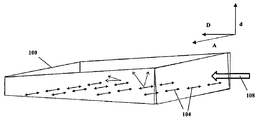
도 3a 내지 도 3c는 광학활성 구조로서(도 3a) 또는 발광된 광을 지향시키기 위한(도 3b 및 도 3c) 웨지 형상의 도광부의 사용을 개략적으로 예시한 도면이다.
도 4a 내지 도 4e는 다색 및/또는 3D 디스플레이/프로젝터 시스템에 사용되는 광학활성 나노로드의 화소 배치의 예를 도시하고 있다.
도 5a 내지 도 5c는 조명장치로부터 출력된 지향성을 갖고 편광된 (또는 부분 편광된) 광을 제공하기 위한 다양한 기술적 솔루션을 사용하는 본 발명의 실시예를 도시하고 있고, 도 5a는 측부 장착된 LED에 의해 광학적으로 펌핑되고, 시준 및 포커싱 조명의 조합을 제공하도록 구성된 조명 장치/유닛을 도시하고 있고, 도 5b는 후방 장착된 LED에 의해 광학적으로 펌핑된 조명 유닛을 도시하고 있고, 도 5c는 시준되거나 부분 시준된 조명을 제공하도록 구성되고 후방 광학 펌핑을 위한 대안의 설계를 갖는 조명 유닛을 도시하고 있다.
도 6은 본 발명의 광학활성 구조에 기초한 백라이트 유닛을 포함하는 LC 패널기반 디스플레이 시스템을 개략적으로 도시하고 있다. BRIEF DESCRIPTION OF THE DRAWINGS For a better understanding of the present invention and to show how it may be carried into effect, reference will now be made, by way of example, to the accompanying drawings, in which: FIG. However, it is not limited thereto.
Figures 1A-1C schematically illustrate three examples of optically active structures of the present invention used in an illumination device such as a backlight source for a display or in any other device using a spatial light modulator, Figure 1B shows an optically active structure in which two different groups of nano-rods are located in different regions, Figure 1C shows a different group of nano- Lt; / RTI > shows a cascade configuration of an optically active structure comprising a rod.
Figures 1d and 1e show theoretical and experimental measurements of the spatial intensity distribution of the light emitted by the layer comprising the aligned optically active nanorods.
Figures 2a-2d show a schematic embodiment of an illumination device of the present invention using an optically active structure exposed to side pumping illumination and configured for use in, for example, a backlight system, Figures 2a and 2b show pumping and output Illumination schemes are illustrated, and Figures 2c and 2d illustrate how optically active nano-rods can be distributed in an optically active structure.
Figs. 3A to 3C are views schematically illustrating the use of an optical active structure (Fig. 3A) or a wedge-shaped light guide portion for directing emitted light (Figs. 3B and 3C).
Figures 4A-4E illustrate examples of pixel placement of optically active nano-rods used in multicolor and / or 3D display / projector systems.
Figures 5A-5C illustrate an embodiment of the invention using various technical solutions for providing polarized (or partially polarized) light with directivity output from a lighting device, Figure 5A shows a side mounted LED 5b shows an illuminated unit optically pumped by a rear mounted LED, and FIG. 5c shows an illuminated device / unit optically pumped by a collimated and focused illumination, Or partially collimated illumination, and has an alternative design for rear optical pumping.
Figure 6 schematically illustrates an LC panel based display system comprising a backlight unit based on the optically active structure of the present invention.
도 1a 내지 도 1c는 조명 장치, 예를 들어, 디스플레이용 백라이트 소스에 사용되는 본 발명의 광학활성 구조(100)의 예를 도시하고 있다. 본 발명의 광학활성 구조(100)는 도 1a 및 도 1b에 도시된 2개의 그룹 G1 및 G2, 그리고 도 1c에 도시된 3개의 그룹 G1, G2, G3와 같은 2개 이상의 그룹의 광학활성 나노로드(즉, 발광을 위해 광학적으로 펌핑된다) 를 포함하고 있다 나노로드의 그룹은 발광된 파장 및/또는 발광의 편광에 있어서 서로 상이하다. 2개 이상의 그룹의 나노로드는 배향/정렬의 하나 또는 두개의 축을 형성하도록 배열되어서, 동일한 그룹의 나노로드는 적어도 하나의 다른 그룹의 것과 실질상 평행하거나 실질상 수직인 정렬의 축과 균일하게 배향된다. 1A-1C illustrate an example of an optically
이와 관련하여, 그룹 G1 및 G2의 나노로드는 배향/정렬 A1 및 A2의 상호 수직인 축을 따라 정렬되고 상이한 파장 λ1 및 λ2의 광을 발광하는 것으로 도 1b에 예시되어 있다. 그러나, 본 발명은 이러한 도면의 조합에 제한되지 않고 상이한 배향이 단지 상이한 그룹의 나노로드의 설명을 위해 상이한 방출 파장과 조합되어 도시되어 있다. In this regard, the nanorods of groups G1 and G2 are illustrated in Figure IB as being aligned along mutually perpendicular axes of alignment / alignment A1 and A2 and emitting light of
도 1a는 본 발명의 실시예에 따른 광학활성 구조(100)를 설명하고 있다. 구조(100)는 단일층(102)(필름)을 형성하고 상이한 그룹 G1, G2의 방출 이방성 나노입자(나노로드)(104A, 104B)를 포함하고 있다. 상이한 그룹 G1 및 G2의 나노로드(104A, 104B)는 펌핑 조명에 노출될 때 상이한 파장의 광을 발광한다. 이러한 예에서, 2개 (또는 보다 많은) 그룹의 나노로드는 필름의 동일한 영역내에 혼합되어 있다. 또한, 이러한 예에서, 상이한 나노로드는 모두 실질상 평행한 축을 따라 정렬되어 있지만, 상이하게 구성되어 (재료 및/또는 크기) 펌핑 광(108)에 응답하여 실질상 유사한 편광을 갖고 상이한 파장의 적어도 2개의 광 성분 L1 및 L2를 방출한다. Figure 1A illustrates an optically
본 발명의 하나의 실시예에서, 나노로드는 예를 들어, UV 또는 바이올렛 펌핑에 응답하여 원색(R,G,B)의 파장을 방출하도록 구성될 수 있거나, 블루 펌핑에 응답하여 적색 및 녹색을 방출하는 나노로드를 포함할 수 있다. 상술된 바와 같이, 나노로드는 하나의 그룹의 나노로드의 정렬의 축이 다른 그룹의 나노로드의 정렬의 축에 평행하거나 수직되도록 정렬될 수 있다. In one embodiment of the invention, the nanorod may be configured to emit wavelengths of primary colors (R, G, B) in response to, for example, UV or violet pumping, or may be configured to emit red and green Lt; RTI ID = 0.0 > nanorods. ≪ / RTI > As described above, the nanorods can be aligned such that the axis of alignment of one group of nanorods is parallel or perpendicular to the axis of alignment of the other group of nanorods.
도 1b는 이전의 예와 유사하게 단일 층(102)(필름)을 형성하고, 상이한 그룹 G1 및 G2의 방출 이방성 나노입자(나노로드)(104,106)를 포함하는 발광 구조(100)를 도시하고 있다. 각 그룹의 나노로드는 균일한 배향을 갖고 있고, 다른 그룹의 나노로드와 비교하여 동일하거나 수직인 배향을 가질 수 있다. 2개 보다 많은 그룹의 나노로드가 존재할 수 있지만 나노로드의 배향의 하나 또는 2개의 수직축이 존재한다. 도 1a의 예와 달리, 도 1b의 예에서, 상이한 그룹의 나노로드는 각각 수직인 배향을 갖고 있고, 이러한 그룹은 공간적으로 분리되어 있고, 특별히 분리된 영역에 위치되어 있다. 또한, 도 1b의 예에서, 나노로드(104, 106)는 상이한 편광을 갖는 광 성분 L1 및 L2의 방출에 의해 펌핑 광(108)에 응답한다. 1B shows a
일부 실시예에서, (직교 편광의 광을 발광하는) 정렬의 수직축과 정렬된 나노로드의 그룹 역시 다색 (백색) 광을 제공하도록 상이한 파장의 광을 발광하는 나노로드를 포함할 수 있다는 것에 주목해야 한다. It should be noted that, in some embodiments, the group of nanorods aligned with the vertical axis of alignment (which emits light of orthogonally polarized light) may also include nanorods that emit light of different wavelengths to provide multicolor (white) light do.
따라서, 본 발명의 조명 장치에서, 광학활성 구조(100)는 보통, 응답하여 나노로드에 의해 방출된 것보다 짧은 파장의 펌핑 또는 여기 광(108)에 노출되는데, 예를 들어, UV 여기 광은 가시광선 스펙트럼에서의 방출을 유발한다. 펌핑 광은 편광되거나 비편광될 수 있고, 광원(110)으로부터 지향된다. 조명 장치에 통합된 광원(110)은 (임의의 적합한 발광기일 수 있는) 발광기, 예를 들어, 단일 LED, 적합한 방식으로 배열된 복수의 LED, CCFL에 의해 구성될 수 있고 및/또는 외부 발광기와 연관된 도광부(예를 들어, 도파로, 광섬유)에 의해 구성될 수 있다. 나노입자(104, 106)는, (편광되거나 비편광된) 펌핑 광(108)에 의해 여기될 때, 상술된 바와 같이, 여기광 보다 긴 파장(보다 짧은 에너지)를 갖고, 나노로드의 정렬축에 의해 형성된 (대략 정렬축에 평행인) 바람직한 편광을 갖고 있는 실질상 편광된 (온전히 또는 일부 편광된) 광(112)을 발광한다. 도 1b의 예에서, 광 성분 L1은 편광축(14)을 갖고 있고 광 성분 L2는 편광축(116)을 갖고 있다. Thus, in the illumination device of the present invention, the optically
일부 실시예에서, 이방성 나노입자는 요구되는 색역을 달성하기 위해 상이한 기본 색에서 방출하도록 하는 조성 및 크기를 가질 수 있다. 예를 들어, 본 출원의 양수인에게 할당된 PCT 공개 번호 WO 2010/095140를 참조하라. 본 발명에 사용되기 적합한 나노로드의 일부 파라미터(재료 조성 및 크기)는 아래에 더 예시되어 있다. In some embodiments, the anisotropic nanoparticles may have a composition and size that allow them to emit in different primary colors to achieve the desired gamut. See, for example, PCT Publication No. WO 2010/095140 assigned to the assignee of the present application. Some parameters (material composition and size) of the nanorods suitable for use in the present invention are further illustrated below.
펌핑 광(108)은 층(102)내의 나노로드(104, 106)에 의해 효율적으로 흡수된 후에, 나노로드의 특징(재료 조성 및 크기)에 의해 형성된 보다 긴 파장의 방출된 광 성분 L1 및 L2로 광(108)을 하향 전환 변환한다. 본 발명의 광학활성 구조는 전기 또는 임의의 다른 자극 없이 광학적으로 여기가능될 수 있다는 것을 이해해야 한다. 나노입자가 구조(100)에 정렬되어 있기 대문에, 발광된 광 L1 및/또는 L2는 실질상 편광되는데(부분적으로 또는 온전히), 예를 들어, 양호하게 형성된 바람직한 편광내의 방출 강도의 적어도 51% 또는 적어도 60%를 갖고 있다. 일부 구성에서, 광학활성 구조는 약 80% 이상의 방출된 광 강도가 바람직한 편광을 갖도록 광을 발광할 수 있다. The pumping
도 1c는 나노로드가 적어도 2개의 이격된 층으로 배열된 광학활성 구조(100)의 또 다른 예를 도시하고 있다. 이러한 3개의 층(102a, 102b, 102c)이 본 예에서 도시되어 있는데, 이것들은 펌핑 광(108)의 전파의 대략적인 방향 D의 축을 따라 이격되어 있다. 상이한 층의 나노로드는 파장 λ0의 펌핑 광(108)에 의해 광학 여기에 응답하여 (상이한 파장 λ1, λ2, λ3으로 마크된) 상이한 색의 광을 발광하는 상이한 이방성 입자(104A, 104B, 104C)를 포함하고 있다. 이러한 구성에서, 층(나노로드를 매입한 매트릭스 또는 나노로드를 갖는 기판)은 펌핑 광의 파장에 대해 부분적으로 투명하다. 예를 들어, 제1(바닥) 층(102A)은 적색 발광 나노로드(104A)(λ1)를 포함하고, 제2(중간) 층(102B)은 녹색 발광 나노로드(104B)(λ2)를 포함하고, 제3(상부) 층(102C)은 청색 발광 나노로드(104C)(λ3)를 포함하고 있다. 이러한 구성은 3개의 층을 포함하기 때문에 보다 복잡하지만, 재흡수 효과로 인해 감소된 손실을 갖는 색역의 보다 양호한 테일링을 허용할 수 있다. 일반적으로 이러한 캐스케이드 구성은 상이한 로드의 적어도 2개의 층/필름에 의해 형성될 수 있다는 것에 주목해야 한다. 펌핑 광(108)은 층(102A)에 충돌하고 층(102A)내의 나노로드에 의해 부분적으로 흡수되어서 이로부터 λ1 광선을 유발한다. 펌핑 광 (일부) 및 발광된 광은 모두 층(102B)쪽으로 전파되고 상호작용하여서 파장 λ2의 광이 발광되도록 하고, 이렇게 생산된 파장 λ0, λ1, λ2의 3개의 광 성분은 층(102C)에 충돌하고, 그 결과 출력광의 일부로부터 사용되거나 여과될 수 있는(즉, 흡수되거나 장치로부터 출력된 광의 전파의 일반적인 방향으로부터 편향될 수 있는) 펌핑 광과 함께 3개의 출력 색 λ1, λ2, λ3을 얻을 수 있다. 이를 위해, 일부 실시예에서, 본 발명의 조명 장치는 옵션으로, 펌핑(여기) 파장을 전송하지만 발출 편광된 색을 반사하는 반사성 필터층을 더 포함할 수 있다. 충돌/펌핑 광을 전송하고 발광된 광을 반사시키는 이러한 파장 선택형 필터 역시 이러한 층들 사이에 배치될 수 있는데, 예를 들어, 파장 λ0를 전송하고 파장 λ1을 반사하는 파장 선택형 필터가 층(102A, 102B) 사이에 배치될 수 있다. 이러한 구성은 방출된 파장이 연속층 사이에서 증가할 때 보다 유용하다. 일부 실시예에서, (바이올렛 광에 대한) 보다 양호한 색 순도 또는 (UV 광에 대한) 안전성을 얻기 위해 잔류 펌프 에너지를 흡수하는 UV (펌핑 광) 차단층이 사용될 수 있다. Figure 1c shows another example of an optically
연속으로 방출된 광 성분의 순서는 상이할 수 있다는 것을 이해해야 한다. 이러한 배열은 연속 발광된 광이 층 마다 증가하거나 감소하는 파장을 갖거나 또 다른 대안의 방식을 갖도록 구성될 수 있다. 이러한 배열에서 연속층이 (펌핑 광의 전파의 대략적인 방향에 대해) 이전층 보다 긴 파장을 방출하도록 되어 있다면, 후속층의 나노로드와 상호작용할 때 이전층에 의해 발광된 광은 연속층으로부터 광 방출을 유발하는 경우가 될 수 있다. It should be appreciated that the order of successive emitted light components may be different. This arrangement can be configured so that successively emitted light has wavelengths that increase or decrease from layer to layer or have another alternative approach. In this arrangement, if the continuous layer is intended to emit a wavelength longer than the previous layer (with respect to the approximate direction of propagation of the pumping light), the light emitted by the previous layer when interacting with the nanorod of the subsequent layer, Or the like.
(상기 구성중 어느 하나의) 구조(100)에 의해 방축된 편광은 투과 모드 LC 패널 예를 들어, 디스플레이 또는 SLM (공간 광변조기) 장치 (도시되지 않음)에 대한 후방 조명으로서 사용될 수 있다. 이러한 편광 특징은 수동형 편광기에 기초한 백라이트 시스템에 일반적인 손실을 감소시킴으로써 에너지를 절감시킬 수 있다. 수동형 편광기를 통과하여 백라이트 에너지의 대략 절반을 손실하는, 공지된 백라이트 시스템에 의해 생성된 비편광된 광에 대조적으로, 본 발명의 조명 장치에서 구조(100)에 의해 생성된 편광은 훨씬 더 적은 손실을 갖고, 따라서 에너지를 절감할 수 있다. 구조(100)로부터의 광이 이미 (부분적으로 또는 온전히) 편광되어 있기 때문에, 투과축에 적합하게 정렬된 수동형 편광기를 효율적으로 통과하여서 훨씬 더 편광의 정도를 증가시킬 수 있다. The polarized light deflected by the structure 100 (of any of the above constructions) may be used as a backlight for a transmissive mode LC panel, for example a display or SLM (spatial light modulator) device (not shown). This polarization feature can save energy by reducing the typical losses in backlight systems based on passive polarizers. In contrast to unpolarized light produced by a known backlight system that passes through a passive polarizer and loses approximately half of the backlight energy, the polarization produced by
상술된 바와 같이, 편광 특성에 더하여, 구조(100)에 의해 발출된 광선은 보통 나노로드의 상응하는 그룹의 정렬축에 수직인 평면에 대하여 작은 각도내에 있는 방향의 강도가 상기 평면에 대한 강도에서보다 크도록 강도가 분포되어 있다. 따라서, 발광된 광의 보다 큰 강도를 갖고, 나노로드의 정렬축에 수직인 전파의 우선 평면이 얻어진다. 이러한 효과는 조명 장치의 사이드로부터 멀어질 수도 있는 광량을 감소시키고 조명에 대한 보다 높은 에너지 효율을 가능케한다. As noted above, in addition to the polarization properties, the light rays emitted by the
이와 관련하여, 나노로드의 장축(정렬축)에 대하여 광 전파의 앙각(Theta) 및 경사각(Psi)의 각각의 함수로서 발광의 강도 분포에 대한 이론값(P1, P1') 및 실험값(P2, P2')을 보여주는 도 1d 및 도 1e에 대해 설명한다. 광학활성 구조로 정렬된 나노로드로부터 발광된 광은 나노로드의 정렬축에 수직인 평면에 대해 작은 각 안에 있는 방향으로 우선 전파한다는 것은 명백하다. 일부 실시예에서, 이러한 발광 방향으로 인해, 나노로드를 포함하는 층은 디스플레이 장치등의 휘도 강화 필름(BEF)에 대한 필요를 제거하는 장점을 가질 수 있다. 추가 지향성 및 포커싱 효과를 제공하기 위해, 나노로드로부터 발광된 광의 경로에서, 즉, LC 패널의 화소 배치와 나노로드를 포함하는 층/구조 사이에서 휘도 강화 필름, 반사기, 또는 광학 컴포넌트의 사용은 여전히 가능하고 유익할 수 있다는 것에 주목해야 한다. 이것은 아래에 더 설명될 것이다. In this connection, theoretical values (P1, P1 ') and empirical values (P2, P1') of the intensity distribution of light emission as a function of the elevation angle (Theta) and the tilt angle (Psi) of the light propagation with respect to the long axis ≪ RTI ID = 0.0 > P2 ') < / RTI > It is clear that the light emitted from the nanorods aligned with the optically active structure propagates first in a direction within a small angle to a plane perpendicular to the alignment axis of the nanorod. In some embodiments, due to this direction of light, the layer comprising the nanorods may have the advantage of eliminating the need for a brightness enhancement film (BEF), such as a display device. In order to provide additional directionality and focusing effects, the use of a brightness enhancement film, reflector, or optical component in the path of light emitted from the nanorod, i.e. between the pixel arrangement of the LC panel and the layer / structure comprising the nanorod, It should be noted that it is possible and beneficial. This will be explained further below.
일반적으로, 편광이 가능한 임의의 나노입자(즉, 이방성 나노입자 또는 나노로드)는 본 발명의 광학활성 구조에서 사용될 수 있다. 이러한 나노로드는 보통 적어도 1.8의 종횡비(그 길이와 단면 치수 사이의 비)를 갖고 있다. 일부 구현예에서, 나노입자는 이방성 반도체 나노로드일 수 있다. 나노로드는 단일 컴포넌트 반도체 나노로드 또는 제1 반도체의 코어와 제2 반도체의 셀층을 갖는 코어/셀 나노로드일 수 있다. 후자의 구조는 나노로드의 방출을 강화시킨다. 코어/멀티셀 나노로드 역시 사용될 수 있고, 셀이 그레이디드 조성을 갖는 코어/셀 구성의 나노입자도 마찬가지로 사용될 수 있다. 대안으로, 나노로드는 하나의 반도체의 구형에 가까운 코어 시드, 또는 로드 형상의 시드가 광선의 이방성 특성을 부여하는 제2 반도체의 로드 형상의 셀에 의해 오버-코팅되는, 시딩된 로드일 수 있다. 이러한 모든 이방성 로드는 구조의 장축에 평행한 축을 따라 편광된 광을 발광한다(편광의 정도의 변화가 가능하다). 시드 자체 역시 긴 형상 또는 (예를 들어, 1.8 이상의 종횡비를 갖는) 로드 구조도 가질 수 있어서, 최종 구조의 편광 정도를 더 강화시킨다. 본 발명의 광학활성 구조에 사용되기에 적합한 시딩된 로드의 일부 예는 본 발명의 양수인에게 양도된 PCT/IL2011/000734에 설명되어 있다. In general, any nanoparticles capable of polarizing (i.e., anisotropic nanoparticles or nanorods) can be used in the optically active structure of the present invention. These nanorods usually have an aspect ratio of at least 1.8 (the ratio between their length and cross-sectional dimensions). In some embodiments, the nanoparticles may be an anisotropic semiconductor nanorod. The nanorod may be a single component semiconductor nanorod or a core / cell nanorod having a core of a first semiconductor and a cell layer of a second semiconductor. The latter structure enhances the emission of nanorods. Core / multi-cell nano-rods may also be used, and nanoparticles of a core / cell configuration in which the cell has a graded composition can be used as well. Alternatively, the nanorod may be a spherical core seed of one semiconductor, or a seeded rod wherein the rod-shaped seed is overcoated by a rod-shaped cell of a second semiconductor that imparts anisotropic properties of the light . All of these anisotropic rods emit polarized light along an axis parallel to the long axis of the structure (a change in degree of polarization is possible). The seed itself may also have a long shape or a rod structure (e.g., having an aspect ratio of 1.8 or greater), thereby further enhancing the degree of polarization of the final structure. Some examples of seeded rods suitable for use in the optically active structure of the present invention are described in PCT / IL2011 / 000734, assigned to the assignee of the present invention.
본 발명의 다양한 실시예에서 사용되는 이방성 나노입자는 일반적으로, 예를 들어, II-VI, III-V 또는 IV-VI 반도체 또는 그 조합의 반도체 재료로 제조될 수 있다. 이러한 재료 역시 본 출원의 양수인에게 양도된 상기 WO 2010/095140에 보다 상세하게 설명되어 있다. 반도체 재료는 CdS, CdSe, CdTe, ZnS, ZnSe, ZnTe, ZnO, GaAs, GaP, GaAs, GaSb, HgS, HgSe, HgTe, InAs, InP, InSb, AlAs, AlP, AlSb, Cu2S, Cu2Se, CuInS2, CuInSe2, Cu2(ZnSn)S4, Cu2(InGa)S4, Ti02, 그 합금 및 그 혼합물로부터 선택될 수 있다. 이러한 재료의 리스트는 (나노로드의 경우에) 로드 재료, (코어/셀 나노로드의 경우에) 코어 및 셀 재료, 또는 시딩된 로드 구조에서의 시드 및 로드 재료를 가리킬 수 있다. 시딩된 나노로드는 긴 셀내의 비대칭으로 위치된 시드(또는 코어)를 가질 수 있다. 코어는 보통 긴 입자 위에 1/4 내지 1/2 길이에 위치될 수 있지만 다른 위치 역시 가능할 수 있다. 시드용 전형적인 크기는 1 내지 20nm 사이일 수 있고 보다 구체적으로 2 내지 10nm 사이일 수 있다. 제1 셀에 더하여, 추가 셀 층이 안정성 및 광학 기능을 위해 포함될 수 있다. 조합은 적용을 위해 필요한 대로 방출 컬러를 제공하도록 튜닝될 수 있다. The anisotropic nanoparticles used in the various embodiments of the present invention may generally be made of semiconductor materials, for example, II-VI, III-V or IV-VI semiconductors or combinations thereof. Such materials are also described in more detail in the above mentioned WO 2010/095140 assigned to the assignee of the present application. Semiconductor material is CdS, CdSe, CdTe, ZnS, ZnSe, ZnTe, ZnO, GaAs, GaP, GaAs, GaSb, HgS, HgSe, HgTe, InAs, InP, InSb, AlAs, AlP, AlSb, Cu 2 S, Cu 2 Se , CuInS 2 , CuInSe 2 , Cu 2 (ZnSn) S 4 , Cu 2 (InGa) S 4 , TiO 2 , alloys thereof, and mixtures thereof. The list of such materials may refer to rod materials (in the case of nanorods), core and cell materials (in the case of core / cell nanorods), or seed and rod materials in the seeded rod structure. The seeded nanorods may have an asymmetrically located seed (or core) within a long cell. The core can usually be located 1/4 to 1/2 length over long particles, but other locations are also possible. Typical sizes for seeds can be between 1 and 20 nm, and more specifically between 2 and 10 nm. In addition to the first cell, additional cell layers may be included for stability and optical functionality. The combination can be tuned to provide the emission color as needed for application.
일부 실시예에서, 표면 리간드는 전체 나노입자 구조를 오버코팅할 수 있다. 추가 리간드 역시 포뮬레이션을 향상시키는데 사용될 수 있다. 널리 사용되는 리간드는 트리옥틸포스핀 옥사이드(TOPO), 트리옥틸포스핀(TOP) 및 트리부틸포스핀(TBP)과 같은 포스핀 및 포스틴 옥사이드; 도데실포스폰산(DDPA), 트리데실포스폰산(TDPA), 옥타데시포스폰산(ODPA) 및 헥실포스폰산(HPA)와 같은 포스폰산; 도데실 아민(DDA), 테트라데실 아민(TDA), 헥사데실 아민(HDA) 및 옥타데실 아민(ODA)과 같은 아민; 헥사데칸 티올 및 헥산 티올과 같은 티올; 및 메르캅토 프로피온산 및 메르캅토언데카노산과 같은 메트캅토 카르복실산을 포함하고 있다. 특정 목적을 위해 주문 제조된 추가 리간드 역시 사용될 수 있다. 전체 나노로드 구조의 길이는 예를 들어, 8 nm 내지 500 nm 사이 그리고 보다 바람직하게는 10 내지 160 nm 사이가 될 수 있다. 로드의 전체 직경은 예를 들어, 1-20 nm 사이 그리고 보다 구체적으로 1-10nm 사이일 수 있다. 전형적인 나노로드는 1.5 보다 큰, 보다 바람직하게는 3 보다 큰 종횡비 길이/직경을 갖고 있다. 크기 및 조성의 제어를 통해, 이방성 나노로드의 방출 컬러는 디스플레이의 요구되는 기본 색을 제공하기 위해 상이한 샘플에 대해 튜닝될 수 있다. 예를 들어, 단일 타입의 로드 샘플은 단색 디스플레이를 위한 단색 백라이트 소스에 사용될 수 있거나, 상이한 컬러에서 방출하는 2개 이상의 상이한 로드의 조합은 컬러 디스플레이에 사용될 수 있다. In some embodiments, surface ligands can overcoat the entire nanoparticle structure. Additional ligands can also be used to enhance formulations. Widely used ligands include phosphines and phosphine oxides such as trioctylphosphine oxide (TOPO), trioctylphosphine (TOP) and tributylphosphine (TBP); Phosphonic acids such as dodecylphosphonic acid (DDPA), tridecylphosphonic acid (TDPA), octadeciphosphonic acid (ODPA) and hexylphosphonic acid (HPA); Amines such as dodecylamine (DDA), tetradecylamine (TDA), hexadecylamine (HDA) and octadecylamine (ODA); Thiols such as hexadecanethiol and hexanethiol; And mercaptocarboxylic acids such as mercaptopropionic acid and mercaptundecanoic acid. Additional ligands tailor-made for specific purposes may also be used. The length of the overall nanorod structure can be, for example, between 8 nm and 500 nm and more preferably between 10 and 160 nm. The overall diameter of the rod may be, for example, between 1 and 20 nm and more particularly between 1 and 10 nm. A typical nanorod has an aspect ratio length / diameter greater than 1.5, more preferably greater than 3. Through control of size and composition, the emission color of the anisotropic nanorods can be tuned for different samples to provide the required basic color of the display. For example, a single type of load sample may be used for a monochrome backlight source for a monochrome display, or a combination of two or more different loads emitting in different colors may be used for a color display.
상술된 바와 같이, 본 발명의 광학활성 구조(100)는 유리 또는 중합체로 제조된 기판 상의 층으로서 제조될 수 있다. 그 두께는 예를 들어, 10nm 내지 수 마이크로미터(예를 들어, 2 마이크로미터 이상) 사이에 있을 수 있다. 대안으로, 구조(100)는 나노로드를 매입하고 요구되는 기계적, 화학적 그리고 광학적 특성을 제공하는 매트릭스 재료를 포함할 수 있다 이러한 매트릭 재료는 (단량체와 같은 액체 또는 반고체 전구체 재료로부터 형성된) 중합체, 에폭시, 실리콘, 유리 또는 실리콘 및 에폭시의 하이브리드와 같은 재료로부터 선택될 수 있다. 중합체의 특정 예는 플루오르화 중합체, 폴리아크릴아미드의 중합체, 폴리아크릴산의 중합체, 폴리아크릴오니트릴의 중합체, 폴리아닐린의 중합체, 폴리벤조페논의 중합체, 폴리의 폴리머(메틸 메타크릴레이트), 실리콘 중합체, 알루미늄 중합체, 폴리비스페놀의 중합체, 폴리부타디엔의 중합체폴리디메틸실록산의 중합체, 폴리에틸렌의 중합체, 폴리이소부틸렌의 중합체, 폴리프로필렌의 중합체, 폴리스티렌의 중합체 및 폴리비닐 중합체로부터 선택된 중합체를 포함하고 있다. 실시예에서, 중합체는 폴리비닐 및 플루오르화 중합체로부터 선택될 수 있다. 다른 실시예에서, 중합체는 폴리비닐-부티랄, 폴리비닐 알콜 또는 폴리메틸 메타아크릴레이트일 수 있다. 이러한 나노로드가 매입된 매트릭스의 두께는 예를 들어, 1 마이크로미터 내지 1 밀리미터이상이 될 수 있다. 이러한 두께는 바람직하게는 10 마이크로미터 내지 800 마이크로미터가 될 수 있고 보다 바람직하게는 50 미크론 내지 350 마이크로미터가 될 수 있다. As discussed above, the optically
실시예에서, 실질상 균일한 소스로부터의 비교적 짧은 파장의 광(예를 들어, UV 또는 바이올렛)은 이방성 나노입자가, 모두 펌핑 광보다 긴 상이한 파장의 광을 방출하는 다수의 팝풀레이션(그룹), 예를 들어, 청, 녹 및 적색에서 방출하는 팝풀레이션을 가질 수 있는 구조(100)에 지향된다. 나노입자는 UV 또는 바이올렛 광의 일부를 흡수할 수 있고 청, 녹 및 적의 보다 긴 파장에서 광을 발광할 수 있어서, 광을 단파장으로부터 보다 긴 파장으로 전환할 수 있다. In an embodiment, relatively short wavelength light (e.g., UV or violet) from a substantially uniform source may be generated by a plurality of populations (groups) in which the anisotropic nanoparticles emit light of different wavelengths, For example, a
정렬 나노로드를 포함하고 펌핑 광(108)에 노출된 광학활성 구조(APEL)(100)를 사용하는 본 발명의 조명 장치(또는 백라이트 시스템)의 다른 실시예를 설명하는 도 2a 내지 도 2d에 대해 설명한다. 이러한 예에서, APEL이 조명되고 층의 적어도 하나의 에지로부터 펌핑되는 소위 사이드 펌핑이 사용된다. 상술된 바와 같이, 임의의 적합한 타입의 내외부 광 발광기로부터 나오는 펌핑 광은 무작위로 편광될 수 있거나 편광되지 않을 수 있다. APEL은 펌핑 광을 흡수하고 이것을 이러한 층에 나타난 나노로드의 파라미터에 따라 결정된 하나 이상의 컬러의 실질상 편광된 광의 발광에 의해 전환한다. 발광된 광의 편광 및 컬러 방식은 특정 시스템의 필요조건에 따라, 예를 들어, LC 기반 디스플레이 시스템의 파라미터에 따라 결정된다. 상술된 바와 같이, 정렬된 나노로드를 포함하는 APEL은 나노로드의 정렬축에 수직인 평면에 대해 작은 각도내에 있는 방향으로 우선적으로 전파하는 광을 발광하고, 디스플레이 장치의 LC 패널에 지향될 수 있다. 2a-2d that illustrate another embodiment of an illumination device (or backlight system) of the present invention that employs an optically active structure (APEL) 100 that includes aligned nanorods and is exposed to pumping light 108 Explain. In this example, so-called side pumping is used wherein the APEL is illuminated and pumped from at least one edge of the layer. As noted above, the pumping light from any suitable type of inner and outer light emitters may or may not be randomly polarized. The APEL absorbs the pumping light and converts it by the emission of substantially phase polarized light of one or more colors determined according to the parameters of the nanorods shown in this layer. The polarization and color scheme of the emitted light is determined according to the requirements of the particular system, for example, according to the parameters of the LC-based display system. As described above, the APEL comprising aligned nanorods emits light that preferentially propagates in a direction that is within a small angle to a plane perpendicular to the alignment axis of the nanorods, and can be directed to the LC panel of the display device .
도면에 도시된 바와 같이, 조명 장치(300)는 보통 이러한 장치로부터 출력된 광의 전파의 일반축 d를 정의하도록 구성되어 있다. 이를 위해, 다양한 적합한 기술이 축 d를 따라 하나 이상의 방향으로, 발광된 광을 편향시키도록 사용될 수 있다. 사이드 펌핑에 대해, 구조(100)로의 펌핑 광의 전파의 일반 방향 축 D과 출력 광의 전파의 일반축 d 사이의 상대적인 배향은 바람직하게 실질상 수직인 축인 차단 축이 되도록 선택된다. As shown in the figure, the
도 2a의 예에서, 반사면(214)은 구조의 하나의 사이드에서 사용되어, 일반축 d쪽으로 상기 사이드에서 발광된 광을 반사한다. 또한, 본 예에서, 구조(100)의 또 다른 사이드에서 층인, 축 광 지향 또는 소위 광 추출 엘리먼트(209)가 장치(300)에 옵션으로 제공된다. 이러한 광 추출 엘리먼트(209)는 파장 선택 편향기 (예를 들어, 격자, 다층 박막 코팅, 다층 중합체 필름) 또는 하나 이상의 굴절 인터페이스를 형성하는 굴절 엘리먼트, 예를 들어, 굴절 렌즈 어레이 또는 구조의 틸팅된 표면(웨지 또는 웨지 형상의 표면)일 수 있다. 광 추출 소자(209)는 외부에 부착된 광학활성 구조(100)와 일체화될 수 있거나, 이격되어 광 추출 소자(209)와 구조(100) 사이의 갭을 생성할 수 있다. 이러한 갭은 굴절율 매칭을 제공하는 재료로 채워질 수 있다. 정렬된 나노로드가 매트릭스 또는 캐리어에 매입된 구조(100) 구성에서, 후자는 펌핑 광 파장에 대해 도파로로서 구성될 수 있다. 도파로 형상이 직방형 단면을 갖는 것으로 도면에 예시되어 있지만 웨지형상, 곡면 형상 및 다른 기하학 형상과 같은 다른 형상이 상술된 목적을 위해 사용될 수 있다는 것에 주목해야 한다. 도 2b는 일반적인 출력 광 전파의 축 d를 따라 2개의 반대 방향으로 출력되는 실질상 편광인 광을 제공하도록 구성된, 본 발명의 조명 장치(300)의 하나 이상의 구성을 예시하고 있다. 이러한 예에서, 광 추출 소자(209)는 광학활성 구조(100)의 2개의 대향면에 제공된다. 이러한 구성은 디스플레이 패널의 양측에 이미지를 제공하도록 구성된 디스플레이 시스템을 위해 사용될 수 있다. In the example of Figure 2a, the
도 2c 및 도 2d는 특정 광학활성 구조 APEL(100)의 평면도를 도시하고 있지만, 도 2a 및 도 2b의 상술된 편광된 조명 장치에 사용되기에 적합한 예를 제한하는 것은 아니다. 도 2c의 예에서, 구조는 캐리어에 매입되고 정렬된 (동일하거나 상이한 그룹의) 나노로드(104)에 의해 형성된 층을 포함하는데, 여기에서 나노로드는 사이드 펌핑 방향 D에 평행한 축을 따라 점차 증가하는 밀도(농도)를 갖도록 분포되어 있다. 캐리어는 도파로로서 구성될 수 있다. 농도 그래디언트 및 가변 농도는 구조로부터의 최적 발광을 위해 선택된다. 도 2c의 이러한 예에서, 나노로드의 농도는 불균일하고 펌핑 광으로부터 멀수록 보다 많은 로드가 존재하고 펌핑 광에 가까울수록 보다 적은 로드가 존재하는 그래디언트가 나타난다. 구조(100)로부터 발광된 편광된 광은 여기 광의 방향 D에 수직인 출력 광의 전파의 일반 축 d을 따라 (예를 들어, 디스플레이 섹션쪽으로 상방향으로) 지향된다. 도 2c 및 도 2d에서, 나노로드는 방향 D에 수직으로 정렬되어 있다. 그러나, 정렬축의 다른 배향도 가능하다는 것에 주목해야 한다. 예를 들어, 나노로드는 도면의 평면에서, 방향 D에대해 45 또는 135도의 방위각을 갖는 축을 따라 정렬될 수 있다. 이러한 정렬축은 때로 편광 설계에서 스크린 제조자에 의해 사용된다. 이러한 구성은 상술된 구조를 따른 펌핑 광의 흡수를 보상할 수 있어서, 실질상 균일한 조명이 전체 장치에 걸쳐 달성될 수 있다. 이러한 나노로드의 공간 분포 역시 구조내의 광 분포에 의해 유발된 2D 효과를 수용하기 위해 특정 2D 패턴을 가질 수 있다. Figures 2c and 2d show a top view of a particular optically
도 2D의 예에서, 구조(100)는 (정렬된 나노로드를 포함하는) 구조(100)의 사이드와 인터페이싱하여/인접하여 위치된 별개의 광 디렉터(312)와 연관되어 있다. 펌핑 조명은 다양한 방향을 따라 구조(100)에 충돌할 수 있다. 특히, 펌핑 조명(펌핑 광(108))은 광 디렉터(312)를 인터페이스하는 것과 반대의 사이드에서 구조(100)에 충돌하도록 특정 일반 방향 D를 따라 구조(100)에 지향될 수 있다. 대안으로 또는 추가로, 펌핑 광은 다른 방향으로부터 구조(100)에 지향될 수 있고, 이러한 하나의 방향이 도 2d에 도시되어 있다. 도 2d에서 펌핑 광(108A)은 방향 D에 수직인 방향으로부터 구조에 입사된다. 이러한 예에서, 정렬된 나노로드는 기판상에 증착되거나 캐리어 내에 매입될 수 있고, 캐리어/기판을 따라 실질상 균일한 농도 분포를 가질 수 있다. 도면에 도시된 바와 같이, 광 지향 소자(312)는 발광된 광 파장에 대한 도파로로서 그리고 도면에 더 설명된 바와 같이 구성되는 것이 바람직하고, 이러한 도파로는 광의 전체 반사를 차단하고 광 추출 층으로서 동작하도록 구성된 웨지 또는 웨지 형상의 표면으로 구성될 수 있다. 도파로(312)는 또한 다른 표면(도 2d의 바닥면) 상에 반사층(바람직하게는 편광 보존 반사기)를 포함할 수 있다. 이러한 구성은 기판에서 보다 적은 수의 이방상 나노입자를 필요로 하기 때문에 보다 경제적일 수도 있다. 편광된 발광된 광내로 광 하향 변환의 효과는 발광된 편광된 광이 요구되는 방향으로 외부 소자(312)에 의해 지향되기 전에 구조(100)에 의해 형성된 제한된 공간에서 발생한다. In the example of FIG. 2D,
나노로드를 여기하여 편광된 광선을 발광시키는 펌핑 광(108)은 다양한 방향으로부터 구조(100)에 지향될 수 있다는 것에 주목해야 한다. 예를 들어, 펌핑 광의 전파의 일반적인 방향 D는 출력 광(즉, 광학활성 구조(100)에 의해 발광된 후에 광 지향 소자(312)와 상호작용된 전파 광)의 전파의 요구되는 일반적인 방향 d에 실질상 평행할 수 있다. 대안으로 또는 추가로, 펌핑 광은 다양한 다른 방향으로부터 광학활성 구조(100)에 충돌할 수 있고, 하나의 이러한 방향은 구조(100)에서 나노로드의 정렬축에 실질상 평행하게 전파하는 펌핑 광(108A)으로서 도 2d에 예시되어 있다. It should be noted that the pumping light 108 that excites the nanorod and emits polarized light may be directed to the
상술된 바와 같이, 본 발명의 조명 장치는 광 추출 소자(예를 들어, 도 2b의 소자(209))를 사용할 수 있다. 웨지 형상의 도광 소자 또는 일반적으로 나노로드에 의해 발광된 광의 광경로에서의 굴절 구조/인터페이스 역시 나노로드의 방출의 방향성을 이용하여 조명 장치의 휘도를 더욱 향상시키는 것이 유리하다. 나노로드의 발광의 방향성은 광 강도의 작은 부분만이 나노로드 정렬축에 수직인 도파로의 2개의 파싯(facet)에 전파하여서 발광된 광의 방향을 전파의 바람직한 방향으로 단순화하는 결과를 초래한다 사실에 주목해야 한다. As described above, the illumination device of the present invention may use a light extraction element (e.g.,
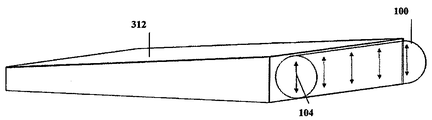
정렬된 나노로드는 웨지형상의 표면이 있는 또는 없는 도파로로서 구성된 외부 광 디렉터를 인터페이싱하는 캐리어/기판에 매입되고 및/또는 웨지 형상의 캐리어에 매입될 수도 있다는 것을 이해해야 한다. 이것은 편광된 조명을 제공하도록 구성될 수 있고 백라이트 조명 시스템에 사용될 수 있는 광학활성 구조를 보여주는 도 3a 내지 도 3c에 예시되어 있다. 도 3a 내지 도 3c의 예는 나노로드에 대한 캐리어(예를 들어, 나노로드는 이러한 캐리어내에 매입되어 있다) 또는 별개의 광 지향 유닛인 웨지 형상의 광 디렉터의 사용을 설명하고 있다. 또한, 나노로드로부터 발광된 광선의 방향성은 발광된 광의 대부분이 웨지형상의 도파로의 수용 각도내에서 전파하는 결과를 초래한다. It should be appreciated that the aligned nanorods may be embedded in and / or embedded in a carrier / substrate interfacing an external optical director configured as a waveguide with or without a wedge-shaped surface. This can be configured to provide polarized illumination and is illustrated in Figures 3A-3C showing an optically active structure that can be used in a backlight illumination system. 3A to 3C illustrate the use of a carrier for the nanorod (e.g., the nanorod is embedded in such a carrier) or a wedge-shaped optical director that is a separate light-directing unit. Further, the directionality of the light beam emitted from the nano-rods results in the fact that most of the emitted light propagates within the receiving angle of the wedge-shaped waveguide.
도 3a는 웨지 형상의 캐리어/매트릭스에 매입된 공통 정렬축 A을 갖는 동일하거나 상이한 그룹의 (예를 들어, 동일하거나 상이한 파장을 방출하는) 복수의 나노로드에 의해 형성된 광학활성 구조(100)를 도시하고 있다. 구조(100)는 사이드 펌핑(108)에 노출되어 있다. 즉, 펌핑 방향 D는 구조의 출력 광 전파 d에 실질상 수직이고 이러한 예에서는 정렬축에도 수직이다. 일반적으로, 사이드 펌핑에 의해, 펌핑 방향은 나노로드의 정렬축에 평행하거나 교차(예를 들어, 수직)하지만, 출력 광 전파 축에 교차하고 있다(바람직하게는 수직이다). 3A shows an optically
도 3b 및 도 3c는 나노로드 또는 나노로드의 캐리어/기판이 웨지형상의 광 디렉터 소자(312)에 인터페이싱하는 광학활성 구조(100)의 2개의 구성을 예시하고 있다. 보다 구체적으로, 구조(100)는 동일한 정렬축을 갖는 동일하거나 상이한 그룹의 나노로드를 포함하는 스트립 형상의 필름 또는 원통형상의 인캡슐레이션이고, 이러한 구조는 웨지(312)의 보다 넓은 사이드와 인터페이싱한다. 나노로드는 웨지 소자의 바닥면에 실질상 수직으로(도 3b) 및 평행하게(도 3c) 정렬되어 있고, 양측의 경우에 상기 인터페이스(웨지의 각 사이드)를 따라 뻗어 있다. 도 3c의 구성은 편광 목적을 위해 유익할 수도 있는데, 그 이유는 발광된 광선의 큰 부분이 순방향으로 도파로에 들어가고, 그 편광 벡터는 슬라브의 면에 대략 평행한 배향을 갖고 있다. 그래서, 슬라브의 사이드로부터의 후속 내부 반사에서, 광의 편광은 크게 영향받지 않을 것이다. 도 3b 및 도 3c에 도시된 것 이외의 나노로드 정렬의 각도는 보다 양호한 편광 출력 및 보다 양호한 커플링을 제공할 수 있기 때문에 사용될 수 있다는 것에 주목해야 한다. Figures 3b and 3c illustrate two configurations of an optically
광을 웨지 형상(또는 슬라브) 도파로에 결합하기 위해 나노로드를 사용하면 QD's와 같은 이방성 나노입자에 비교하여 다양한 장점이 있음에 주목해야 한다. 보다 구체적으로, 나노로드가 도 3c에 도시된 바와 같이 원통형 인캡슐레이션의 장축에 실질상 평행하게 정렬된 일부 실시예에서, 광선의 큰 비율이 순방향으로 도파로에 들어가고, 그 편광 벡터는 슬라브의 면에 대략 평행한 배향을 갖는다. 그래서, 슬라브의 사이드로부터의 후속 내부 반사에서, 광의 편광은 실질상 보존되어 편광된 광 출력을 제공하고 상당한 에너지를 절감하게 한다. 위에서 예시된 바와 같이, 일부 다른 실시예에서, 웨지 (또는 슬라브)의 평면에 수직의 배향을 갖는 나노로드를 포함하는 스트립 형상의 필름 또는 원통형상의 인캡슐레이션은 도파로와 펌핑 소스 사이의 도파로의 넓은 단부에 위치되어 사용될 수 있다. 최종 광선의 방향성은 보다 많은 광이 도파로의 수용각도 내에 있다는 것을 의미한다. It should be noted that the use of nanorods to couple light into a wedge-shaped (or slab) waveguide has a number of advantages over anisotropic nanoparticles such as QD's. More specifically, in some embodiments where the nanorods are aligned substantially parallel to the long axis of the cylindrical encapsulation, as shown in Figure 3c, a large proportion of the light enters the waveguide in a forward direction, As shown in Fig. Thus, in subsequent internal reflection from the side of the slab, the polarization of light is substantially preserved, providing a polarized light output and saving considerable energy. As illustrated above, in some other embodiments, a strip-shaped film or cylindrical encapsulation, including nano-rods having an orientation perpendicular to the plane of the wedge (or slab) As shown in Fig. The directionality of the final beam means that more light is within the acceptance angle of the waveguide.
본 발명이 3D 디스플레이/프로젝터에 대한 광원은 물론 컬러 편광된 광원으로서 어떻게 사용될 수 있는지를 예시하는 도 4a 내지 도 4e에 대해 설명한다. 4A-4E, which illustrate how the present invention can be used as a color polarized light source as well as a light source for a 3D display / projector.
도 4a는 이격된 영역에 위치된 상이한 이방성 나노입자(104A, 104B, 104C)의 복수의 그룹(이러한 예에서는 3개의 그룹, G1, G2, G3)을 갖는 층의 형태로 광학활성 구조(100)를 도시하고 있다. 각 영역은 특정 컬러로 발광하는 이방성 나노입자를 포함하는데, 예를 들어, 나노로드(104A)의 영역은 적색 발광 나노로드를 포함하고, 나노로드(104B)는 녹색 발광 나노로드를 포함하고, 나노로드(104C)는 청색 발광 로드를 포함한다. 모든 그룹/영역내의 모든 나노로드는 동일한 정렬축을 따라 정렬되어 있어서, 동일한 편광을 갖는 광을 발광한다. 이러한 배열은 컬러 디스플레이에 대한 백라이트를 제공할 수 있다. 물론, 색역을 증가시키기 위해 3개 보다 많은 그룹/영역(상이한 이방성 나노입자로부터의 색)을 갖는 것이 가능하다. Figure 4a illustrates an optically
도 4b는 도 4a의 상술된 예와 대략 유사하게 구성된 광학활성 구조(100)를 도시하고 있다. 즉, 나노로드는 상이한 그룹으로 되어 있고, 일반적으로 R에서 영역의 2차원 어레이로 배열되어 있다. 그러나, 도 4b의 예에서, 적어도 하나의 축을 따라 (이러한 예에서는 양측의 축을 따라) 국부적으로 인접한 영역의 나노로드는 실질상 수직인 정렬축 A1 및 A2를 갖고 있다. 컬러 특징에 대해, 이러한 구성에서 물론 사용될 수 있는데, 예를 들어, 국부적으로 인접한 영역은 상이한 발광 파장의 나노로드를 포함할 수 있거나, 각 영역은 상이하게 발광하는 나노로드의 혼합물을 포함할 수 있다. 또 다른 실시예에서, 구조는 상이하게 정렬된 나노로드의 하지만 동일한 발광 파장의 그룹을 각각 갖는 2개 이상의 이러한 층의 캐스케이드를 포함할 수 있고, 상이한 층은 상이하게 발광하는 나노로드를 포함하고 있다. 도 4c는 도 4a 및 도 4b의 상술된 예와 대략 유사하게 구성된 광학활성 구조(100)를 예시하고 있다. 그러나, 도 4c의 예에서, 어레이의 하나의 축을 따라 인접 영역에 위치된 나노로드의 그룹은 발광된 광의 파장에서 상이하고, 어레이의 다른 축을 따라 인접 영역에 위치된 나노로드의 그룹은 정렬의 실질상 수직인 축과 정렬되어 있다. 이러한 구성은 컬러링된 3D 디스플레이/프로젝터 시스템에 사용될 수 있다. FIG. 4B shows an optically
빌보드 디스플레이와 같은 다양한 디스플레이 시스템이 상이한 컬러의 스트라이프의 형태로 컬러링된 조명을 사용할 수 있다. 이것은 나노입자가 (스트라이프의 형태로) 이격된 긴 영역(502, 504, 506)에 배치되어 있는 광학활성 구조(100)의 2개의 구성을 개략적으로 보여주는 도 4d 및 도 4e에 예시되어 있다. 이전의 예와 마찬가지로, 스트라이프 배열은 대략 3개(일부 경우에 4개 이상의) 기본 색을 갖는 컬러 디스플레이 디바이스의 것과 일치하여, 상이한 컬러의 화소의 배열을 제공한다. 각 스트라이프는 상이한 기본 색에서 발광하는 나노로드의 상이한 팝풀레이션(그룹)을 포함하고 있다. 도 4d에서, 각 스트라이프의 나노로드는 그 인접한 스트라이프의 나노로드에 평행하게 정렬되어, 상술된 바와 같이, 발광된 광의 상이한 컬러로 이제까지 설명된 모든 특성을 갖는 이방성 편광을 제공한다. 도 4e에서, 일부 인접한 스트라이프는 (서로 수직인) 나노로드의 정렬축만이 상이하고, 일부 다른 인접한 스트라이프는 나노로드의 발광된 컬러 및 정렬이 상이하다. 도 4b 및 도 4c의 구성와 마찬가지로, 도 4e의 구성은 3D 디스플레이 시스템에 사용하기에 적합하다. 이러한 구성은, 보통 큰 디스플레이 시스템에 적합하고, 디스플레이 시스템에서의 컬러 필터 층에 대한 필요를 제거하거나 적어도 실질적으로 감소시킬 수 있다. 따라서, 일반적으로, 이러한 예에서, 편광 및/또는 컬러에서 상이한 그룹이 대안의 방식으로 배열된다. Various display systems, such as billboard displays, can use colored light in the form of stripes of different colors. This is illustrated in Figures 4D and 4E, which schematically illustrate two configurations of optically
특별히 도시되지 않았지만, 3차원 디스플레이에서 본 발명의 광학활성 구조(100)를 사용할 때, 이웃중 적어도 하나의 것에 수직인 편광의 나노로드의 그룹에 의해 구성된, 화소의 선형 편광은 적합한 편광 회전기(예를 들어, 1/4 파장판)를 사용하여 시계방향 및 반시계방향 원형 편광으로 전환될 수 있다는 것에 주목해야 한다. 이것은 예를 들어, 원형 편광 3D 유리와 같은 3D 뷰잉 장치와 호환되도록 이루어진다. Although not specifically shown, the linear polarization of a pixel, constituted by a group of polarizing nano-rods perpendicular to at least one of the neighbors, when using the optically
이제, 조명장치(400)로부터 지향성 및 편광된 출력 광을 제공하기 위한 다양한 기술 솔루션을 사용하는 본 발명의 추가 실시예를 예시하는 도 5a 내지 도 5c에 대해 설명한다. 도 5a, 도 5b 및 도 5c에 도시된 장치는 편광되고 지향성을 갖는 광을 제공하기 위해 대형 디스플레이용 화소 소자로서 기능할 수 있다. 조명 장치(400)는 하나의 축을 따라 균일하게 정렬된 나노로드(2개의 축을 따른 정렬 역시 가능하다)를 포함하는, 본 발명에 따라 구성된 APEL 구조를 채용한다. 도 5a, 도 5b, 도 5c는 광학활성 구조가 원통형상의 구성을 갖고 있고 나노로드의 장축 또는 구조(100)의 정렬축이 도면의 평면에 수직으로 뻗어 있는 장치를 도시하고 있다. (반사되거나 통과하면서) 구조(100)에 의해 발광된 편광을 실질상 유지하도록 구성된 반사성 및/또는 굴절 광학 소자/인터페이스를 사용하고 정렬된 나노로드를 사용함으로써, 출력 광(112')은 실질상 나노로드의 정렬의 원래 축을 따라 편광될 수 있다. 5A-5C illustrating a further embodiment of the present invention using various technology solutions for providing directional and polarized output light from the
APEL 구조(100)는 발광된 광의 파장 만큼 상이한 나노로드의 하나 이상의 그룹을 포함할 수 있다. 나노로드의 그룹은 균일하게 정렬되어 하나의 그룹의 나노로드는 다른 그룹의 나노로드에 평행하거나 수직으로 정렬되어 있다. The
따라서, 조명 장치(400)는 기판상에 증착되거나 캐리어에 매입된 균일하게 정렬된 나노로드를 포함하는 APEL 구조(100) 및, 발광된 광과 연관된 광 지향/편향 유닛(214)을 포함하고 있다. 조명 장치(400)는 (도면의 평면에 수직인) 도 5a에 도시된 바와 같이 사이드로부터, 또는 도 5b 및 도 5c에 도시된 바와 같이 도면의 평면내에 임의의 방향으로부터 APEL 구조로 지향될 수 있는 펌핑 광(108)에 의해 여기된다. 펌핑 광(108)은 펌핑 광(108)의 시준, 포커싱, 또는 다른 조작/광 처리를 위해 사용되는, (도 5b에 도시된) 부착된 소자(111)(예를 들어, 렌즈, 굴절 렌즈)를 포함할 수 있는 광원(110)(예를 들어, LED. 또는 상술된 바와 같은 임의의 다른 광원 또는 도광부)으로부터 APEL(100)에 지향된다. 다른 실시예에서, 예를 들어, 도 5c에서, 조명 장치(400)는 광원(110)으로부터 나오는 펌핑 광과 연관되고 펌핑 광을 APEL(100)에 지향하도록 구성된 광 지향/편향 유닛(314)을 포함하고 있다. 나노로드의 지향성 및 다이폴형 방출로 인해, 구조(100)로부터 발광된 광의 대부분은 (나노로드의 정렬축에 수직인) 도면의 평면에 대해 작은 각도내에 있는 다양한 방향으로 전파하고, 이에 따라, 조명 장치는 실질상 원통형(원통형상) 구성을 가질 수 있고, 정렬축을 따라 대칭을 이룰 수 있다. 따라서, 예를 들어, 원통형 대칭 굴절, 반사형 및 회절 소자가 채용될 수 있지만, 예를 들어, 구형 미러 또는 렌즈의 상이한 기하학 형상을 갖는 다른 광학 소자 역시 사용될 수 있다. Thus, the
본 발명의 일부 실시예는 (3D 디스플레이 시스템용과 같은) 서로에 수직으로 정렬된 나노로드의 그룹을 포함하는 영역을 사용할 수 있다. 이러한 실시예에서, 조명 장치는 각각 도 5a 내지 도 5c에 도시된 바와 같이 구성된 조명 유닛의 어레이에 기초하고, 인접 유닛이 수직 평면을 따라 뻗도록 배열되어 있다. 마찬가지로, 구형 또는 원통형의 광학 렌즈가 부착된 로드의 장축을 따라 배열된 다수의 이격된 광원을 사용하는 것이 가능하다. 또한, 광원 소자(110) 및 광학 부착 렌즈(111)가 상이한 대칭을 가질 수 있다. Some embodiments of the present invention may use regions that include a group of nanorods aligned perpendicularly to one another (such as for a 3D display system). In this embodiment, the illumination device is based on an array of illumination units each configured as shown in Figs. 5A to 5C, and adjacent units are arranged to extend along a vertical plane. Likewise, it is possible to use a plurality of spaced light sources arranged along the long axis of a rod with a spherical or cylindrical optical lens attached thereto. Further, the
광 지향 유닛(214)은 광 편향기(122)(예를 들어, 원통형-원형 또는 원통형-포물선형 미러) 및 광 유닛(120)(예를 들어, 하나 이상의 렌즈, 보통, 원통형 렌즈 시스템)을 포함하고 있다. 광학활성 구조(100)의 나노로드는 광원(110)에 의해 발광된 펌핑 광(108)에 의해 여기된다. 광학 펌핑은 나노로드의 정렬축에 수직인 평면에 대해 작은 각내에 있는 (방향으로) 축을 따라 우선 전파하는 광(112)을 발광하도록 나노로드를 여기한다. 발광된 광(112)의 일부 광 성분은 광 반사기(122)로부터 광 유닛(120)으로 반사되고, 일부 광 성분은 광 유닛(120)으로 직접 전파한다. 광 지향 유닛(214)은 출력 광의 편광 상태를 실질상 유지하면서 장치로부터의 발광된 광의 전파의 적합하게 형성된 일반적인 방향을 제공하도록 사용된다. 광 지향 유닛(214)은 또한 광의 누설을 감소시키고 따라서 에너지를 절감시킨다. 따라서, APEL 구조(100)로부터 발광된 광은 조명 장치(400)의 사용을 위해 적합한 전파의 적합한 사전결정된 일반적인 방향으로 지향된다. The
도 5a 및 도 5b는 렌즈 유닛(1200과 조합되어 동작할 때, 시준 및 포커싱 효과의 조합, 즉, 시준된 광(112') 및 포커싱 광(112") 출력을 제공하는 포물선형 단면을 갖는 광 편향기(122)의 사용을 설명하고 있다. 이와 대조적으로, 도 5c의 예에서, 편향 유닛(122)은 원형 단면의 반사 미러이어서 장치로부터 시준된 출력 광(112')을 제공한다. 광학활성 구조(100)는 렌즈 유닛(120)의 전방 초점면에 위치되는 바람직하고, 그 중심이 광 편향기(122)의 곡면의 중심과 일치하도록 위치되는 것이 바람직하다. 이러한 구성은 포커싱 컴포넌트 없이, 실질상 평행한 광 출력(시준된 광(112'))을 제공한다. 5A and 5B illustrate a light beam having a parabolic cross section that provides a collimated and focused effect combination when operating in combination with the lens unit 1200, i.e., collimated light 112 'and focusing light 112' In the example of Figure 5C, the
광 편향기(122) 및 렌즈 유닛(120)의 사용을 위한 상기 예는 넓게 이해되어야 하고 다양한 다른 구성(에를 들어, 다각 광 편향기등)이 사용될 수 있다는 것에 주목해야 한다. 광학 소자와 APEL 구조(100)의 상대적 위치는 장치로부터 출력된 광의 요구되는 조명 패턴 및 각도 분포에 따라 상이할 수 있다는 것에 주목해야 한다. It should be noted that the above example for use of the
도 5c는 광 편향기(126)(예를 들어, 반사기), 펌핑 광(108)과 연관되고 광 지향 유닛(314)에 포함된 광 유닛(124)(예를 들어, 하나 이상의 렌즈)의 사용을 예시하고 있다. 도 5c는 또한, 시준된 출력 광(122')을 제공하도록 구성된 원통형 광 편향기(122)의 사용을 예시하고 있다. 광학활성 구조(100)의 나노로드는 광 지향 유닛(314)에 의해 구조(100)에 지향된 펌핑 광(108)에 의해 여기된다. LED와 같은 비지향성 광원(110)로부터 발광된 펌핑 광은 다양한 방향으로 전파하고, 구조쪽으로 광 편향기(126)에 의해 반사되면서 렌즈 유닛(124)에 의해 구조(100)에 포커싱될 수 있다. 광 편향기(122)는 파장 선택될 수 있는데, 즉, 발광된 광(112)의 파장 범위의 광을 반사하면서 펌핑 광(108)의 파장 범위의 광을 전송하도록 구성될 수 있고(예를 들어, 이색 광소자), 예를 들어, 장치로부터 출력된 광의 요구되는 패턴/분포를 제공하도록 구성된 실질상 원형 단면(또는 임의의 다른 기하학 형상)을 갖는 원통형 광 편향기로서 구성될 수 있다. 광 편향기(122)는 파장 선택형 전송(예를 들어, 이색 미러의 영역)의 패턴(예를 들어, 이격된 영역)을 가질 수 있어서, 발광된 광에 대한 반사기로서 (APEL에 대면하는) 편향기의 내면의 다른 부분을 떠나면서 APEL로의 펌핑 광 전파를 위한 파장 선택 영역(개구)를 제공할 수 있다. 일부 실시예에 따라, 광 편향기(122)는 내부 반사면을 갖는 원통형 광 편향기의 영역에 의해 둘러싸인 색선별 (파장 선택형) 편평한 영역을 가질 수 있다. 5C illustrates the use of an optical deflector 126 (e.g., a reflector), a
도 5a 내지 도 5c에 도시된 조명 장치(400)로부터 나오는 광은 (도 2a 또는 도 3a의 소자(312)와 같은) 광 지향 소자에 더 결합될 수 있다. 조명 장치(400), 또는 광 지향 유닛(214)은 출력 광이 사전결정된 요구되는 조명 패턴/광 분포에 따라 선택된 수용각(130) 안에 있도록 구성될 수 있다. 보다 구체적으로, 렌즈 유닛(120)의 전방 초점면이 광 지향 유닛(122)(바람직하게는 포물선형)의 (공간에서 포인트 또는 라인일 수 있는) 초점 영역과 일치하도록 구성되어 있고 APEL 구조(100)가 그 위에 위치되어 있다면, 발광된 광은 (도 5b에 도시된 바와 같이) 시준되고 포커싱된 광의 조합일 것이다. 대안으로, 렌즈 유닛(120)의 전방 초점 평면이 광 지향 유닛(122)의 초점 영역 위에 (광 전파의 일반 방향에 대해 하류에) 단거리에 있도록 구성되어 있고 APEL 구조(100)가 초점면의 위치 사이에 있다면, 렌즈 유닛(120)은 다양한 정도의 포커싱 광을 제공한다. 역으로, 렌즈 유닛(120)의 전방 초점면이 포물선형 편향 유닛(122)의 초점 영역 아래에(광 전파의 일반적인 방향에 대해 상류에) 있다면, 발광된 광(112')의 일부 또는 모두는 광학활성 구조(100)의 정밀한 위치에 따라, 분산될 것이다. 대부분, 조명 장치의 정확한 구성, 즉, (다양한 초점 거리를 갖는) 이러한 광 지향/추출 광소자는 물론, 광 지향/추출 소자에 대한 구조(100)의 위치는 얻어지는 출력 광(112')의 요구되는 각도 분포에 따라 선택된다. 출력 광의 최적 분산/수렴 각도는 조명 패턴, 에너지 효율 및 조명 장치/유닛의 전체 치수 사이의 균형을 유지하면서 달성될 수 있다. The light emanating from the
이제, 본 발명의 광학활성 구조 APEL(100) 및 펌핑 광원(110)을 포함하는 (조명 장치를 구성하는) 백라이트 유닛을 사용하는 디스플레이 시스템(200)의 특정 예(하지만 이에 제한되지는 않는다)를 개략적으로 도시하는 도 6에 대해 설명한다. 시스템(200)은 일반적으로 디스플레이부(201)(화소 어레인지먼트) 및 백라이트부(203)로 나눌 수 있다. 광학활성 구조(100)는 다색 발광을 위해 구성되는 것이 바람직하고, 상기 예시된 구성의 어느 하나(예를 들어, 평면 또는 캐스케이드)일 수 있다. 화소 어레인지먼트(201)는 LC 패널(204)로서 구성되고, 이에 따라 시스템(200)은 LC 패널의 출력부에서 제1 편광기(206)를 포함한다. 또한, 시스템(200)은 옵셔널 컬러 필터(216), 및 조명 장치(203)의 출력부에 제2 편광기(202)를 포함한다. A specific example (but not limited to) of a
사용시, 펌핑 광원(110)으로부터의 (파장 λ0을 갖는) 단파장 비편광선은 디스플레이 장치용 요구되는 색역(예를 들어, 들어, 파장 λ1, λ2, λ3)을 갖는 편광된 광을 발광하는 광학활성 구조(100)를 조명한다. 구조(100)로부터 발광된 편광된 광은 광 편향기(202)를 통과한 후에 액정 구조(204)를 통과하고 편광기(206)를 통과한다. LC 재료는 RGB 필터 및 이들에 부착된 편광기(도시되지 않음)를 가질 수 있는 2개의 유리판 사이에 배치될 수 있다. 편광기(202)는 깨끗하고, 보다 온전한 편광 상태를 얻기 위해 사용될 수 있다. LC 구조(204)는 화소의 출력을 변조하기 위해 공간 광 변조기로서 사용될 수 있다. LC 구조(204)의 화소 셀은 광 통과를 차단할 수 있거나 대안으로, 광 편광의 각도를 변경할 수 있어서, 이렇게 수정된 광이 편광기(206)에 흡수되도록 하고, 전송된 광의 강도를 변조시킨다. 시스템(200)에는, 광 분포를 공간적으로 균일하게 하고, 구조(100)에 직접 광학적으로 부착된 경우에는 광 추출을 도울 수 있는 확산기(208), 휘도 강화 필름(BEF)(210), 또는 듀얼 휘도 강화 필름(DBEF)(212)과 같은 하나 이상의 광소자가 옵션으로 더 제공된다. 소자(210, 212)는 광을 재활용함으로써 휘도를 향상시키도록 사용될 수 있다. 본 특정 예에서, 시스템(200)은 또한 펌핑 광원(110)의 타측에 구조(100)로부터 반대에 위치된 반사기(214)(반사기는 제공은 옵션이다)를 포함하고 있다. 반사기는 광원 및 다른 소자로부터 오는 펌핑 광의 일부를 재순환시킬 수 있다. 별개의 컴포넌트로서 도시되었지만, 다양한 층/구조는 이들의 실질적 기능을 유지하면서 상이한 구성으로 결합되거나 조합될 수 있다는 것을 이해해야 한다. 컬러 필터층(216)은 옵션이고 컬러 디스플레이의 컬러 화소를 형성하기 위해 사용된다. In use, the short wavelength light rays (with wavelength? 0 ) from the pumping
다음은 특정 광학활성 구조의 전파를 위한 특정 예인데, 이에 제한되지는 않는다. The following are specific examples for the propagation of certain optically active structures, but are not limited thereto.
예 1: 정렬된 나노로드를 중합체 매트릭스 내에 포함하는 광학활성 구조가 준비되었다. 나노로드는 중합체 필름의 기계적 스트레칭에 의해 중합체 필름 내에 정렬되었다. 제1 단계로서, 나노로드는 톨루엔(2.4ml) 및 폴리비닐부티랄(PVB, 200mg)의 단량체 용액과 혼합되었다. 이러한 필름내의 나노로드 농도는 보통 PVB 중량의 중량 대비 0.5-3%의 범위의, 필름에 추가된 양에 의해 제어되었다. 그다음, 블록은 성형으로 용융되고 12 시간 동안 진공 환경에서 건조되도록 허용된 중합체/나노로드로부터 주조되었다. 스트레칭 단계 동안, 블록은 기계적 스트레칭 장치에 놓였다. 스트레칭 동안, 샘플은 샘플의 전방에 적외선 램프를 배치함으로써 1100까지 가열되었다. 그다음, 샘플은 하나의 방향으로 천천히 당김으로써(0.5mm/분) 이방성으로 스트레칭되었다. 일단 필름이 8의 팩터에 의해 길어지면, 스트레칭은 중단되었고 이러한 스트레칭된 필름은 그 새로운 구성으로 동결되었다. 기계적 스트레칭 동작에 의해 나노로드 정렬은 스트레칭 방향으로 우선적으로 지향된다. 이로 인해 바람직하게는 정렬축을 따라 편광된 광을 발광하는 정렬된 나노로드를 갖는 독립형 중합체 필름을 얻을 수 있다. 이러한 광선은 측정되었고 이러한 광선의 편광 값이 추출되었다. 정렬축에 평행한 발광과 수직인 발광 사이에 측정된 편광비는 특정 상태에 따라 2.4-3.3이었다. 보다 높은 값은 보다 많은 스트레칭에 의해 달성될 수 있다. Example 1: An optically active structure containing aligned nanorods in a polymer matrix was prepared. The nanorods were aligned in the polymer film by mechanical stretching of the polymer film. As a first step, the nanorods were mixed with a monomer solution of toluene (2.4 ml) and polyvinyl butyral (PVB, 200 mg). The nanorod concentration in these films was controlled by the amount added to the film, usually in the range of 0.5-3% relative to the weight of PVB weight. The blocks were then cast from the polymer / nanorods allowed to melt in the mold and allowed to dry in a vacuum environment for 12 hours. During the stretching step, the block was placed in a mechanical stretching device. During stretching, the sample was heated to 110 0 by placing an infrared lamp in front of the sample. The sample was then anisotropically stretched by slowly pulling it in one direction (0.5 mm / min). Once the film was lengthened by a factor of 8, stretching was discontinued and this stretched film was frozen in its new configuration. By mechanical stretching operation, the nanorod alignment is preferentially oriented in the stretching direction. This results in a stand-alone polymer film preferably having aligned nanorods that emits polarized light along the alignment axis. These rays were measured and the polarization values of these rays were extracted. The measured polarization ratio between the emission parallel to the alignment axis and the vertical emission was 2.4-3.3 depending on the particular state. Higher values can be achieved by more stretching.
예를 들어, 단색 디스플레이에 대해, 620nm에서 발광하는 CdSe 시드를 갖는 CdS 로드가 적용되었다(로드 크기 41 x 5.3nm). 2개의 컬러 디스플레이에 대해, 상이한 치수의 CdSe 시드를 갖는 CdS 로드의 2개의 샘플의 혼합물이 적용되었다. 제1 샘플은 630nm에서 발광하였고(적색 로드, 로드 크기 36 x 7 nm) 제2 샘플은 550nm에서 발광하였다(녹색 로드, 로드 크기 25 x 3nm). For example, for monochrome displays, a CdS rod with a CdSe seed emitting at 620 nm was applied (rod size 41 x 5.3 nm). For two color displays, a mixture of two samples of CdS rod with CdSe seeds of different dimensions was applied. The first sample emitted at 630 nm (red rod, rod size 36 x 7 nm) and the second sample emitted at 550 nm (green rod, rod size 25 x 3 nm).
이러한 예에서 사용된 시딩된 로드가 광선의 낮은 자체 흡수율을 제공한다는 것에 주목하는 것이 중요하다. 이것은 DBEF 필름이 보다 높은 편광이 달성될 때까지 여러번 원치않은 편광된 광을 재순환하는데 사용되는 방식에서 특히 중요하다. 심지어 작은 자체 흡수율로 인해 DBEF는 비효율이 될 수 있다. 또한, 적색 발광 나노로드는 도트와 비교하여 적색 영역에서 매우 작은 흡수율을 갖고 있다. 이것은 적색이 청색 또는 UV 입력에 의해서만 여기되기 때문에 적색과 혼합된 녹색을 갖는 나노로드를 포함하는 피름에서 보다 양호한 성능을 허용한다. 따라서, 추가적으로, 나노로드의 캐릭터는 이러한 필름이 정규 퀀텀 도트로 준비된 유사한 필름에 비교하여 우월하도록 한다. 이러한 나노로드의 일부 특징은 본 발명의 양수인에게 양도된 WO/2011/092646에 개시되어 있고, 이러한 공개 내용은 일부 예에 대해 언급되어 여기에 통합되어 있다. It is important to note that the seeded rod used in this example provides a low self-absorption rate of the light beam. This is particularly important in the manner in which the DBEF film is used to recycle undesired polarized light many times until a higher polarization is achieved. Even a small self-absorption rate can make DBEF inefficient. Further, the red light emitting nano-rod has a very small absorption rate in the red region as compared with the dot. This allows for better performance in a scene involving nanorods with green mixed with red because red is excited only by blue or UV input. Thus, in addition, the characters of the nano-rods make such films superior to similar films prepared with regular quantum dots. Some features of such nanorods are disclosed in WO / 2011/092646, assigned to the assignee of the present invention, which disclosure is incorporated herein by reference in some instances.
백라이트 유닛을 구성하기 위해, 상기 광학활성 구조는 청색 발광 광원(450nm, 20mW, 2.4 칸델라 근방에서 발광)에 배치되었다. 녹색 및 적색 로드의 농도는 필요한 색역을 제공하도록 튜닝되었고 2개의 컬러 디스플레이용 백라이트로서 사용될 수도 있다. 다른 구현예에서, 농도는 풀컬러 디스플레이를 제공하는 것을 통해 청색광의 일부가 전송될 수 있도록 하기 위해 튜닝되었다. 활성 이방성 나노입자층 후의 광은 광학활성 구조의 메인 정렬축에 평행한 전송축을 갖는 편광기에 통과되었다. 이것은 광을 위한 보다 온전한 편광 특성을 얻기 위해 이루어졌다. 비편광된 광으로 인한 광의 손실은 높은 에너지 효율을 제공하는 이러한 경우에 최소이었다. 그다음, 광은 액정 변조기 및 디스플레이의 나머지 부분으로 전송되었다. To construct a backlight unit, the optically active structure was arranged in a blue luminescent light source (450 nm, 20 mW, emission near 2.4 candelas). The green and red rod concentrations are tuned to provide the required gamut and may be used as backlights for two color displays. In another embodiment, the concentration was tuned to allow a portion of the blue light to be transmitted through providing a full color display. Light after the active anisotropic nanoparticle layer was passed through a polarizer having a transmission axis parallel to the main alignment axis of the optically active structure. This was done to obtain better polarizing properties for light. The loss of light due to unpolarized light was minimal in this case to provide high energy efficiency. The light was then transmitted to the liquid crystal modulator and the rest of the display.
예 2: 독립형 나노로드를 포함하는 광학활성 구조가 준비되었다. 사용된 로드는 67 x 5 nm의 치수를 갖고 622nm에서 발광하는, CdSe 시드를 가진 CdS 로드이었다. 이러한 로드는 유리 기판 또는 중합체 필름에 정렬되었다. 제1 방법에서, 나노로드는 용액으로부터 유리에 증착된 후 벨벳 클로스에 의해 러빙 기술에 의해 정렬되었다. 대안으로, 로드의 용액은 러빙 프로세스 동안 적용되었다. 이러한 벨벳 클로스는 나노로드 정렬을 우선적으로 러빙의 방향을 따라 지향시킨다. 이로 인해 바람직하게 정렬축을 따라 편광된 광을 발광시키는 정렬된 나노로드를 가진 층을 얻을 수 있다. 이것은 단색 디스플레이에서 사용될 수도 있다. Example 2: An optically active structure comprising a stand-alone nanorod was prepared. The rod used was a CdS rod with a CdSe seed, having a dimension of 67 x 5 nm and emitting at 622 nm. These rods were aligned to a glass substrate or a polymer film. In the first method, the nanorods were deposited from the solution onto glass and then aligned by means of a velvet cloth by rubbing technique. Alternatively, the solution of the rod was applied during the rubbing process. These velcro closure preferentially directs the nanorod alignment along the direction of the rubbing. This results in a layer with aligned nanorods that emits polarized light, preferably along the alignment axis. It may also be used in monochrome displays.
디스플레이용 2-컬러 백라이트 유닛이 제3 컬러로 기능하는 필름을 통과하는 비흡수되는 청색 광선을 갖는 디스플레이용 3 컬러 백라이트 유닛으로 확장될 수 있다는 것이 증명되었다. 상이한 치수의 CdSe 시드를 갖는 CdS 로드의 2개의 샘플의 혼합물이 적용되었다. 622nm에서 발광하는 제1 샘플(적색 로드), 및 540nm에서 발광하는 제2 샘플(녹색 로드)은 광선이 2개의 피크를 보여주는 조합을 생성한다. 나노로드의 광선의 편광성 및 방향성은 아래에 설명된 바와 같이 측정되었다. It has been demonstrated that a two-color backlight unit for a display can be extended to a three-color backlight unit for a display having a non-absorbed blue light ray passing through a film that functions as a third color. A mixture of two samples of CdS rod with CdSe seeds of different dimensions was applied. A first sample (red rod) emitting at 622 nm and a second sample (green rod) emitting at 540 nm produce a combination in which the light beam shows two peaks. The polarization and directionality of the light rays of the nanorods were measured as described below.
622nm 광선을 갖는 샘플 필름은 스펙트럼의 청색 영역에서 발광하는 LED에 의해 조명되었다. 이러한 층에 의해 발광된 광은 필터를 통과하여, 전송된 청색 광을 제거하고 광선을 분리하였다. 그다음, 이러한 광선의 강도는 CCD를 사용하여 측정되었다. 편광기에 의해 2개의 편광을 따른, 즉, 나노로드의 방향과 그 직교 방향으로의 강도는 물론 전체 강도 모두를 측정할 수 있다. 요구되는 편광을 갖는 광 강도의 직교 편광의 광 강도의 비로 정의된 편광비(PR)는 3.3:1이었다. 나노로드의 긴 치수와 동일한 방향의 축을 가진 편광기를 통과할 때, 나노로드의 광선은 정규 비편광된 광에 대한 50% 투과율과 비교하여 77%의 투과율을 나타냈다(편광기 자체에서 발생하는 손실은 무시하였다). 다이폴형의 발광기에 대해 예측되는 바와 같이, 광선은 나노로드의 정렬축에 수직인 평면에 대해 작은 각도내에 있는 축을 따른 방향으로 보다 농도가 높은 것으로 발견되었고, 나노로드의 팁 방향으로 감소하지만, 수평 평면내의 배향각 방향으로 대략 균일하다. 먼저, 나노로드가 필름내에 완전하게 순서지정되지 않고 단일 파라미터, SIGMA, 분포에 대한 표준 편차에 의해 특징지어진 방향의 분포를 따라 정렬된다고 가정된 이론적 모델이 고안되었다. 또한, 개별적인 레벨에서, 나노로드는 순수한 다이폴로서 발광하도록 가정되지 않았고, 이러한 개별적인 레벨은 개별적인 로드에 대해 무한의 (최대) PR 값으로 전환된다. 오히려, 용액내의 나노로드의 이전 측정값이 개별적으로 취해진 로드에 대한 6의 PR 값에 영향을 주었다. 이론적 분석을 통한 비교에 의해 러빙을 통해 19 도의 SIGMA 값을 갖는 정렬을 얻을 수 있음을 알 수 있다. 나노로드(130)의 장축에 평행하게 편광된 광의 강도의 앙각(쎄타)와의 편차 및 수치 시뮬레이션(140)에 대한 매치가 도 1d에 표시되어 있다. 나노로드(150)의 장축에 평행하게 편광된 광의 강도의 방위각(Psi)와의 편차 및 수치 시뮬레이션(160)에 대한 상응하는 매치가 도 1e에 표시되어 있다. The sample film with the 622 nm light was illuminated by an LED emitting in the blue region of the spectrum. The light emitted by this layer passes through a filter to remove the transmitted blue light and isolate the light beam. Then, the intensity of these rays was measured using a CCD. The polarizer can measure both the direction along the two polarizations, that is, the direction of the nano-rod and the intensity in the direction orthogonal thereto as well as the total intensity. The polarization ratio (PR) defined by the ratio of the optical intensity of the orthogonal polarization of the light intensity with the required polarization was 3.3: 1. When passing through a polarizer with an axis in the same direction as the long dimension of the nanorod, the light of the nano-rod showed a transmittance of 77% compared to the 50% transmittance for the normal unpolarized light (the loss occurring in the polarizer itself is negligible ). As expected for dipole-type emitters, the light rays were found to be more dense in the direction along the axis that is within a small angle to the plane perpendicular to the alignment axis of the nanorods and decrease in the tip direction of the nanorods, And is substantially uniform in an orientation angle direction in a plane. First, a theoretical model has been devised in which the nanorods are assumed to be aligned along a distribution in a direction characterized by a single parameter, SIGMA, and a standard deviation of the distribution, without being completely ordered within the film. Also, at the individual levels, the nanorods are not assumed to emit as pure dipoles, and these individual levels are converted to infinite (maximum) PR values for the individual loads. Rather, previous measurements of the nanorods in solution affected the PR value of 6 for the separately taken rod. By comparison through theoretical analysis, it can be seen that alignment with SIGMA values of 19 degrees can be obtained through rubbing. The deviation from the elevation angle (theta) of the intensity of the light polarized parallel to the long axis of the nano-
예상되는 바와 같이, 광선은 자오선 평면에서 보다 강하고, 팁의 방향에서 감소하고, 방위각 방향으로 대략 균일한 것으로 발견되었다. 이론적 분석을 통한 비교를 통해 러빙이 10도의 시그마를 갖는 정렬을 달성할 수 있음을 알 수 있다. 극성 및 방위각과의 강도 및 편광의 편차 그리고 수치 시뮬레이션에 대한 매치가 도 1d 및 도 1e에 도시되어 있다. As expected, the rays were stronger in the meridian plane, decreased in the direction of the tip, and found to be approximately uniform in azimuthal direction. It can be seen from the comparison through the theoretical analysis that rubbing can achieve alignment with a sigma of 10 degrees. Variations in intensity and polarization with polarity and azimuth and matches for numerical simulations are shown in Figures 1d and 1e.
백라이트 유닛을 구성하기 위해, 상기 활성 이방성 나노입자층이 청색 발광 광원(460nm 근방에서 발광)에 증착되었다.녹색 및 적색 로드의 농도는 필요한 색역을 제공하기 위해 튜닝되었고 2 색 디스플레이로서 사용될 수도 있다. 다른 실현에서, 농도는 청색광의 일부가 전송될 수 있도록 튜닝되었다. 광학활성 구조 이후의 광은 광학활성 구조의 메인 정렬축에 평행한 전송축을 갖는 편광기를 통과하였다. 이것은 광에 대한 보다 온전한 편광 특성을 얻기 위해 이루어졌다. 중요한 것은 비편광된 광으로 인한 광의 손실이 높은 에너지 효율을 제공하는 이러한 경우에 최소이었다는 사실이다. 그다음, 광은 액정 변조기 및 디스플레이의 나머지부에 전송되었다. To constitute a backlight unit, the active anisotropic nanoparticle layer was deposited on a blue luminescent light source (luminescence in the vicinity of 460 nm). The green and red rod concentrations were tuned to provide the required gamut and could also be used as a two color display. In another implementation, the concentration was tuned so that a portion of the blue light could be transmitted. The light after the optically active structure passed through a polarizer having a transmission axis parallel to the main alignment axis of the optically active structure. This was done to obtain more intense polarization characteristics for light. It is important to note that the loss of light due to unpolarized light was minimal in this case to provide high energy efficiency. Then, the light was transmitted to the liquid crystal modulator and the rest of the display.
예 3: 독립형 나노로드를 포함하는 광학활성 구조가 준비되었다. 이러한 로드는 본 출원의 양수인에게 양도된 상술된 WO/2010/095140에 기술된 바와 같은 패턴화된 전극을 갖는 유리 기판에 정렬되었다. 이러한 방법에서, 나노로드는 전극 사이의 교류 전계를 인가하면서 용액으로부터 유리에 증착되었다. 용액의 건조 동안, 우선적으로 나노로드는 인가된 전계의 방향과 평행하게 정렬되었다. 이것은 바람직하게 정렬축을 따라 편광된 광을 발광하는 바람직하게 정렬된 나노로드를 갖는 층을 생성한다. 편광비에 대한 전형적인 값은 2 내지 4.7 사이에 있었는데, 각 컬러 발광기는 사용된 특정 타입의 나노로드, 및 나노로드 증착 및 정렬 상태에 따라 상이한 편광비를 가질 수 있다. 백라이트 유닛을 구성하기 위해, 상기 활성 이방성 나노입자층이 청색 발광하는 광원(460nm 근방에서 발광)에 배치되었다. 녹색 및 적색 로드의 농도는 필요한 색역을 제공하도록 튜닝되었고, 2 색 디스플레이로서 사용될 수도 있다. 또 다른 실현에서, 농도는 청색광의 일부가 전송될 수 있도록 하기 위해 튜닝되었다. 광학활성 구조 이후의 광은 광학활성 구조의 메인 정렬축에 평행한 전송축을 갖는 편광기를 통과하였다. 이것은 이러한 광에 대한 보다 온전한 편광 특성을 얻기 위해 이루어졌다. 중요한 것은, 비편광된 광으로 인한 광의 손실이 높은 에너지 효율을 제공하는 이러한 경우에 최소였다는 사실이다. 그다음, 광은 액정 변조기 및 디스플레이의 나머지부에 전송되었다. Example 3: An optically active structure containing a stand-alone nanorod was prepared. These rods were arranged on glass substrates having patterned electrodes as described in the above-mentioned WO / 2010/095140 assigned to the assignee of the present application. In this way, the nanorods were deposited on glass from solution while applying an alternating electric field between the electrodes. During drying of the solution, preferentially the nanorods were aligned parallel to the direction of the applied electric field. This preferably produces a layer with a preferably aligned nanorod that emits polarized light along the alignment axis. Typical values for the polarization ratio were between 2 and 4.7, where each color light emitter could have a different polarization ratio depending on the particular type of nano-rod used and the nanorod deposition and alignment conditions. To constitute a backlight unit, the active anisotropic nanoparticle layer was disposed in a light source (light emission in the vicinity of 460 nm) emitting blue light. The green and red rod concentrations are tuned to provide the required gamut and may be used as a two-color display. In another realization, the concentration was tuned to allow a portion of the blue light to be transmitted. The light after the optically active structure passed through a polarizer having a transmission axis parallel to the main alignment axis of the optically active structure. This was done to obtain more intense polarization characteristics for this light. It is important to note that the loss of light due to unpolarized light was minimal in this case to provide high energy efficiency. Then, the light was transmitted to the liquid crystal modulator and the rest of the display.
따라서, 본 발명은 다양한 컬러 및/또는 직교 편광의 편광된 광을 디스플레이/프로젝터에 제공하기 위해 하나 또는 2개의 축을 따라, 균일하게 정렬된 나노로드에 기초한 광학활성 구조를 사용하는 편광된 광원에 대한 새로운 접근법을 제공한다. 이러한 접근법은 수동형 편광기로 백라이트를 지향시키는 주지된 방법에 비해 유리하다. 실제, 본 발명은 백라이트의 편광으로 인해 상당히 향상된 에너지 효율을 제공하는데, 그 이유는, 본 발명의 광학활성 구조가 편광된 광을 발광하고 따라서 온전히 편광된 광에 대해 거의 2의 팩터 만큼 편광기에 전송되는 광을 증가시킬 수 있다. 이러한 증가는 부분적으로 편광된 광에 대해서조차 상당히 클 수 있다. 예를 들어, 액정 제1 편광기의 것과 동일한 축을 갖는 90% 편광된 광에 대해, 팩터는 1.8=90/50이다. 이것은 복잡하고 고비용의 DBEF 필름의 성능과 동일하거나 심지어 초월할 수 있는 저렴하고 효율적인 해결책을 제시하다. 또한, 본 발명은 백라이트 시스템 구조를 단순화시키는데, 그 이유는 광학활성 구조가 이미 편광된 광을 발광하여서, 보다 적은 층으로 비교가능하고 훨신 더 양호한 성능을 얻을 수 있기 때문이다. 이것은 발광 강도 각도 편차가 다이폴과 유사하다는 점에서 광학활성 구조 내의 나노로드의 추가 특성과 관련되어 있다. 적은 광은 장축 방향으로 발광되고 보다 강한 광선이 장축 방향과 수직인 방향으로 제공된다. 이것은 원하는 방향으로 발광된 광의 보다 양호한 사용을 가능하게 한다. 또한, 본 발명은 매우 크고 유연한 색역에 대한 포텐셜을 갖는 백라이트 시스템을 제공하는데, 그 이유는 요구되는 기본 색에서 발광하는 나노재료의 조합을 활성 이방성 나노입자층에 배치하는 것이 가능하기 때문이다. Accordingly, the present invention is directed to a polarized light source that uses an optically active structure based on uniformly aligned nanorods along one or two axes to provide polarized light of various colors and / or orthogonally polarized light to the display / projector. Provide a new approach. This approach is advantageous over known methods of directing a backlight with a passive polarizer. Indeed, the present invention provides significantly improved energy efficiency due to the polarization of the backlight, since the optically active structure of the present invention emits polarized light and is therefore transmitted to the polarizer with a factor of approximately 2 for fully polarized light Light can be increased. This increase can be considerably large even for partially polarized light. For example, for 90% polarized light having the same axis as that of the liquid crystal first polarizer, the factor is 1.8 = 90/50. This presents an inexpensive and efficient solution that can be the same or even exceed the performance of complex and costly DBEF films. The present invention also simplifies the backlight system structure because the optically active structure emits already polarized light, so that fewer layers are comparable and much better performance can be obtained. This is related to the additional properties of the nanorods in the optically active structure in that the luminescence intensity angle deviation is similar to a dipole. The less light is emitted in the major axis direction and the stronger light ray is provided in the direction perpendicular to the major axis direction. This enables better use of light emitted in the desired direction. The present invention also provides a backlight system having a very large and flexible potential for gamut because it is possible to place a combination of nanomaterials that emit light in the required basic color in the active anisotropic nanoparticle layer.
Claims (31)
반사, 확산 및 굴절 구조부 또는 인터페이스 중 적어도 하나를 포함하는 적어도 하나의 광 추출 특징부를 포함하고,
동일한 그룹의 상기 나노로드는 적어도 하나의 다른 그룹의 나노로드의 제2 정렬축에 평행하거나 수직인 제1 정렬축으로 균일하게 정렬되고, 상기 복수의 나노로드는 서로 평행하거나 또는 수직인 하나 또는 2개의 정렬축을 갖고,
상기 광 추출 특징부는 상기 발광되는 광의 상기 편광을 보존하도록 구성되는 것을 특징으로 하는 광학활성 구조.A plurality of optically active nano-rods formed by nanorods arranged in at least two groups different from each other in at least one of a wavelength of light emitted in response to pumping light, an alignment axis and a polarization caused thereby; And
At least one light extraction feature comprising at least one of a reflective, diffusing, and refractive structure or interface,
Wherein the nanorods in the same group are uniformly aligned with a first alignment axis parallel to or perpendicular to a second alignment axis of at least one other group of nanorods and wherein the plurality of nanorods are aligned one or two Having a number of alignment axes,
Wherein the light extracting feature is configured to preserve the polarization of the emitted light.
반사, 확산 및 굴절 구조부 또는 인터페이스 중 적어도 하나를 포함하는 적어도 하나의 광 추출 특징부;를 포함하고,
동일한 그룹의 나노로드는 다른 그룹의 나노로드의 정렬축에 수직인 정렬축과 균일하게 정렬되어 있고,
상기 광 추출 특징부는 발광된 광의 편광을 보존하도록 구성되어서, 2개의 직교 편광의 광을 발광하는 광학활성 구조를 제공하는 것을 특징으로 하는 광학활성 구조. A plurality of optically active nano-rods formed by two groups of nano-rods; And
At least one light extraction feature comprising at least one of a reflective, diffuse and refractive structure or interface,
The nanorods of the same group are uniformly aligned with the alignment axis perpendicular to the alignment axis of the nanorods of the other group,
Wherein the light extracting feature is configured to preserve the polarization of the emitted light to provide an optically active structure that emits light of two orthogonally polarized light.
반사, 확산 및 굴절 구조부 또는 인터페이스 중 적어도 하나를 포함하는 적어도 하나의 광 추출 특징부;를 포함하고,
상기 복수의 광학활성 나노로드는 공통 정렬축을 따라 균일하게 배향되고,
상기 광 추출 특징부는 상기 발광된 광의 편광을 보존하도록 구성되어서, 광학활성 구조는 상기 펌핑 광에 응답하여 적어도 2개의 상이한 파장의 편광된 광을 발광하는 것을 특징으로 하는 광학활성 구조.A plurality of optically active nano-rods formed by at least two groups of nano-rods having different wavelengths of light emitted in response to pumping light; And
At least one light extraction feature comprising at least one of a reflective, diffuse and refractive structure or interface,
Wherein the plurality of optically active nano rods are uniformly oriented along a common alignment axis,
Wherein the light extracting feature is configured to preserve the polarization of the emitted light so that the optically active structure emits at least two different wavelengths of polarized light in response to the pumping light.
Applications Claiming Priority (3)
| Application Number | Priority Date | Filing Date | Title |
|---|---|---|---|
| US41036210P | 2010-11-05 | 2010-11-05 | |
| US61/410,362 | 2010-11-05 | ||
| PCT/IL2011/050005 WO2012059931A1 (en) | 2010-11-05 | 2011-11-06 | Polarizing lighting systems |
Publications (2)
| Publication Number | Publication Date |
|---|---|
| KR20130140689A KR20130140689A (en) | 2013-12-24 |
| KR101995309B1 true KR101995309B1 (en) | 2019-07-02 |
Family
ID=45375470
Family Applications (1)
| Application Number | Title | Priority Date | Filing Date |
|---|---|---|---|
| KR1020137010519A KR101995309B1 (en) | 2010-11-05 | 2011-11-06 | Polarizing lighting systems |
Country Status (7)
| Country | Link |
|---|---|
| US (1) | US9529228B2 (en) |
| EP (1) | EP2635934B1 (en) |
| JP (1) | JP6084572B2 (en) |
| KR (1) | KR101995309B1 (en) |
| CN (1) | CN103201674B (en) |
| IL (1) | IL225057A (en) |
| WO (1) | WO2012059931A1 (en) |
Families Citing this family (110)
| Publication number | Priority date | Publication date | Assignee | Title |
|---|---|---|---|---|
| JP5753796B2 (en) | 2009-02-23 | 2015-07-22 | イサム・リサーチ・デベロツプメント・カンパニー・オブ・ザ・ヘブルー・ユニバーシテイ・オブ・エルサレム・リミテッド | Optical display device and method thereof |
| US20130112942A1 (en) | 2011-11-09 | 2013-05-09 | Juanita Kurtin | Composite having semiconductor structures embedded in a matrix |
| US9557573B2 (en) | 2012-05-09 | 2017-01-31 | Merck Patent Gmbh | Three dimensional display system |
| KR101347896B1 (en) * | 2012-06-26 | 2014-01-10 | 엘지디스플레이 주식회사 | Quantum rod luminescent display device |
| CN105378517B (en) | 2013-06-06 | 2019-04-05 | 富士胶片株式会社 | Optics chip part and the image display device for using the optics chip part |
| US9722147B2 (en) | 2013-07-03 | 2017-08-01 | Pacific Light Technologies Corp. | Network of semiconductor structures with fused insulator coating |
| US9249354B2 (en) | 2013-07-03 | 2016-02-02 | Pacific Light Technologies Corp. | Network of semiconductor structures with fused insulator coating |
| JP6153895B2 (en) * | 2013-07-22 | 2017-06-28 | 富士フイルム株式会社 | Liquid crystal display |
| JP6153813B2 (en) * | 2013-08-12 | 2017-06-28 | 富士フイルム株式会社 | Liquid crystal display |
| US9594240B2 (en) * | 2013-12-06 | 2017-03-14 | Samsung Electronics Co., Ltd. | Lighting apparatus, and optical inspection apparatus and optical microscope using the lighting apparatus |
| KR20160113658A (en) * | 2014-01-29 | 2016-09-30 | 코닝 인코포레이티드 | Laser featured glass for display illumination |
| WO2015144288A1 (en) * | 2014-03-26 | 2015-10-01 | Merck Patent Gmbh | A polarized light emissive device |
| EP3126903A1 (en) | 2014-04-02 | 2017-02-08 | Yissum Research Development Company of the Hebrew University of Jerusalem Ltd. | Polarized light source device |
| US9703031B2 (en) * | 2014-04-28 | 2017-07-11 | Rambus Delaware Llc | Light guide and lighting assembly with array of rotated micro-optical elements |
| CN106661444A (en) | 2014-06-13 | 2017-05-10 | 默克专利股份有限公司 | Mixture, nano fiber, and polarized light emissive film |
| US10670229B2 (en) * | 2014-06-26 | 2020-06-02 | Yissum Research Development Company Of The Hebrew University Of Jerusalem Ltd. | Emitting film with improved light-out coupling |
| JP2016012024A (en) * | 2014-06-27 | 2016-01-21 | 富士フイルム株式会社 | Light conversion film, method for manufacturing same, laminate, and method for manufacturing same |
| JP2016012084A (en) | 2014-06-30 | 2016-01-21 | 富士フイルム株式会社 | Liquid crystal display device |
| JP2016012047A (en) * | 2014-06-30 | 2016-01-21 | 富士フイルム株式会社 | Liquid crystal display device |
| JP6353410B2 (en) * | 2014-07-18 | 2018-07-04 | 富士フイルム株式会社 | Polymerizable liquid crystal composition, wavelength conversion film, wavelength conversion member and method for producing the same, backlight unit, liquid crystal display device |
| KR102220405B1 (en) | 2014-07-25 | 2021-02-25 | 삼성전자주식회사 | Optical elements and electronic devices including the same |
| DE102014117312A1 (en) | 2014-08-28 | 2016-03-03 | Osram Opto Semiconductors Gmbh | Optoelectronic arrangement and lighting device |
| KR102293604B1 (en) * | 2014-09-04 | 2021-08-24 | 삼성전자주식회사 | Photoluminescent liquid crystal displays |
| JP6842418B2 (en) | 2014-09-22 | 2021-03-17 | イッサム リサーチ ディベロップメント カンパニー オブ ザ ヘブライ ユニバーシティー オブ エルサレム リミテッドYissum Research Development Company Of The Hebrew University Of Jerusalem Ltd. | LC-based optical display system |
| KR102200347B1 (en) * | 2014-09-25 | 2021-01-08 | 엘지디스플레이 주식회사 | Quantum rod display device and Method of fabricating the same |
| JP6380979B2 (en) * | 2014-09-29 | 2018-08-29 | 富士フイルム株式会社 | Liquid crystal composition, polarized light emitting film, wavelength conversion member and method for manufacturing the same, backlight unit, liquid crystal display device |
| KR101944850B1 (en) * | 2014-11-13 | 2019-02-07 | 엘지디스플레이 주식회사 | Quantum rod solution composition, Quantum rod sheet and Display device including the same |
| CN104360425B (en) * | 2014-11-24 | 2017-02-22 | 京东方科技集团股份有限公司 | Optical film layer, light emitting device and display device |
| US20160187730A1 (en) * | 2014-11-26 | 2016-06-30 | The Hong Kong University Of Science And Technology | Polymer Film With Geometrically Anisotropic Nanostructures |
| KR20170094419A (en) * | 2014-12-15 | 2017-08-17 | 메르크 파텐트 게엠베하 | A polarized light emissive device |
| CN107108479B (en) * | 2014-12-23 | 2020-07-24 | 加利福尼亚大学董事会 | Three-dimensional structures of mesogenic ligand-functionalized nanoparticles and methods of making and using the same |
| US9897854B2 (en) | 2015-01-05 | 2018-02-20 | Samsung Display Co., Ltd. | Liquid crystal display having improved color reproduction |
| KR102277941B1 (en) * | 2015-01-05 | 2021-07-16 | 삼성디스플레이 주식회사 | Liquid crystal display device |
| DE102015101216A1 (en) * | 2015-01-28 | 2016-07-28 | Osram Opto Semiconductors Gmbh | Optoelectronic arrangement with radiation conversion element and method for producing a radiation conversion element |
| KR20230041087A (en) * | 2015-02-04 | 2023-03-23 | 메르크 파텐트 게엠베하 | Electronic element and display |
| JP6453662B2 (en) * | 2015-02-09 | 2019-01-16 | 富士フイルム株式会社 | Liquid crystal composition, polarized light emitting film, wavelength conversion member and method for producing the same, backlight unit, liquid crystal display device |
| CN107851684B (en) * | 2015-03-13 | 2020-03-24 | 陶氏环球技术有限责任公司 | Nanostructured material method and apparatus |
| CN104793418A (en) * | 2015-04-30 | 2015-07-22 | 京东方科技集团股份有限公司 | Array substrate and manufacturing method thereof and display device |
| TWI564603B (en) * | 2015-05-13 | 2017-01-01 | 明基材料股份有限公司 | Quantum rod film |
| US10266760B2 (en) | 2015-05-13 | 2019-04-23 | Osram Opto Semiconductors Gmbh | Composition of, and method for forming, a semiconductor structure with multiple insulator coatings |
| JP6672624B2 (en) * | 2015-07-14 | 2020-03-25 | 大日本印刷株式会社 | Quantum dot sheet, backlight and liquid crystal display |
| EP3325571B1 (en) | 2015-07-17 | 2019-05-01 | Merck Patent GmbH | Luminescent particle, ink formulation, polymer composition, optical device, fabrication thereof, and use of the luminescent particle |
| US10795207B2 (en) * | 2015-07-29 | 2020-10-06 | Lg Display Co., Ltd. | Quantum rod layer, method of fabricating the same and display device including the same |
| EP3356888B1 (en) | 2015-09-29 | 2021-03-03 | Merck Patent GmbH | A photosensitive composition and color converting film |
| TWI550326B (en) | 2015-10-28 | 2016-09-21 | 明基材料股份有限公司 | Quantum rod backlight module |
| CN105301837B (en) * | 2015-11-11 | 2019-02-26 | 深圳市华星光电技术有限公司 | Liquid crystal display |
| CN105527753B (en) * | 2016-02-14 | 2019-01-11 | 京东方科技集团股份有限公司 | A kind of backlight module, display device, lighting apparatus |
| US10072991B2 (en) * | 2016-03-17 | 2018-09-11 | The United States Of America As Represented By The Secretary Of The Army | Lanthanide and silicon-based nanoparticle pressure sensor and system |
| CN105652461A (en) * | 2016-03-31 | 2016-06-08 | 京东方科技集团股份有限公司 | Polarized light source and display device |
| US20190153307A1 (en) | 2016-03-31 | 2019-05-23 | Merck Patent Gmbh | A color conversion sheet and an optical device |
| US10234723B2 (en) * | 2016-05-05 | 2019-03-19 | Samsung Electronics Co., Ltd. | Backlight unit including anisotropic semiconductor nanocrystal particles, production method thereof, and electronic device including the same |
| CN109313366B (en) * | 2016-05-10 | 2021-11-05 | 香港科技大学 | Photoalignment quantum rod reinforced film |
| US20170356612A1 (en) * | 2016-06-13 | 2017-12-14 | Edgar Hosiel Leon Esquivel | Anti-glare system for vehicles |
| US10717927B2 (en) | 2016-07-14 | 2020-07-21 | Samsung Electronics Co., Ltd. | Indium-based quantum dots and production methods thereof |
| KR102520299B1 (en) | 2016-08-01 | 2023-04-10 | 메르크 파텐트 게엠베하 | Photosensitive composition, color conversion medium, optical device and manufacturing method thereof |
| CN106356470A (en) * | 2016-09-13 | 2017-01-25 | Tcl集团股份有限公司 | Core/shell semiconductor nanorod film, polarization light emitting diode and preparation method thereof |
| CN106356465B (en) * | 2016-10-27 | 2020-01-14 | Tcl集团股份有限公司 | Efficient QLED device based on nanorods and display |
| WO2018087125A1 (en) | 2016-11-11 | 2018-05-17 | Merck Patent Gmbh | Light luminescent particle |
| WO2018096135A1 (en) | 2016-11-28 | 2018-05-31 | Merck Patent Gmbh | Composition comprising a nanosized light emitting material |
| JP2020514432A (en) | 2016-12-15 | 2020-05-21 | メルク パテント ゲゼルシャフト ミット ベシュレンクテル ハフツングMerck Patent Gesellschaft mit beschraenkter Haftung | Semiconducting luminescent nanoparticles |
| WO2018108765A1 (en) | 2016-12-15 | 2018-06-21 | Merck Patent Gmbh | Method for preparing a nanosized light emitting semiconductor material |
| WO2018114761A1 (en) | 2016-12-20 | 2018-06-28 | Merck Patent Gmbh | Optical medium and an optical device |
| WO2018146120A1 (en) | 2017-02-10 | 2018-08-16 | Merck Patent Gmbh | Semiconductor nanosized material |
| JP2020515693A (en) | 2017-03-31 | 2020-05-28 | メルク パテント ゲゼルシャフト ミット ベシュレンクテル ハフツングMerck Patent Gesellschaft mit beschraenkter Haftung | Semiconducting luminescent nanoparticles |
| CN110959113B (en) * | 2017-05-12 | 2023-07-25 | 澳大利亚国立大学 | Frequency conversion apparatus and process |
| US11542432B2 (en) | 2017-05-23 | 2023-01-03 | Merck Patent Gmbh | Method for synthesizing a semiconducting nanosized material |
| KR102652514B1 (en) | 2017-06-08 | 2024-03-28 | 메르크 파텐트 게엠베하 | Compositions Comprising Semiconductor Light-Emitting Nanoparticles Having Thiol-Functional Surface Ligands |
| US11746284B2 (en) | 2017-06-29 | 2023-09-05 | Merck Patent Gmbh | Composition comprising a semiconducting light emitting nanoparticle |
| WO2019025392A1 (en) | 2017-08-03 | 2019-02-07 | Merck Patent Gmbh | Quantum yield recovery |
| WO2019081404A1 (en) | 2017-10-24 | 2019-05-02 | Merck Patent Gmbh | Quantum dots based on indium phosphide |
| WO2019081401A1 (en) | 2017-10-24 | 2019-05-02 | Merck Patent Gmbh | Quantum dots having a high absorption |
| WO2019081402A1 (en) | 2017-10-24 | 2019-05-02 | Merck Patent Gmbh | Quantum dots having a high quantum yield |
| EP3717592B1 (en) | 2017-11-30 | 2022-05-04 | Merck Patent GmbH | Composition comprising a semiconducting light emitting nanoparticle |
| WO2019115489A1 (en) | 2017-12-14 | 2019-06-20 | Merck Patent Gmbh | Semiconducting light emitting nanoparticle |
| JP7395487B2 (en) | 2018-02-22 | 2023-12-11 | メルク パテント ゲゼルシャフト ミット ベシュレンクテル ハフツング | semiconducting nanoparticles |
| JP7118711B2 (en) | 2018-04-10 | 2022-08-16 | キヤノン株式会社 | Light source device and image projection device |
| WO2019211257A1 (en) | 2018-05-03 | 2019-11-07 | Merck Patent Gmbh | Crosslinked ligands |
| WO2019215059A1 (en) | 2018-05-09 | 2019-11-14 | Merck Patent Gmbh | Semiconducting nanoparticle |
| WO2019224134A1 (en) | 2018-05-23 | 2019-11-28 | Merck Patent Gmbh | Semiconducting nanoparticle |
| WO2019224182A1 (en) | 2018-05-24 | 2019-11-28 | Merck Patent Gmbh | Formulation comprising particles, a polymer and an organic solvent |
| KR20210038940A (en) | 2018-08-03 | 2021-04-08 | 메르크 파텐트 게엠베하 | Composition |
| WO2020043661A1 (en) | 2018-08-28 | 2020-03-05 | Merck Patent Gmbh | Method for synthesizing a semiconducting material |
| KR20210076084A (en) | 2018-10-15 | 2021-06-23 | 메르크 파텐트 게엠베하 | nanoparticles |
| WO2020099284A1 (en) | 2018-11-14 | 2020-05-22 | Merck Patent Gmbh | Nanoparticle |
| EP3898884A1 (en) | 2018-12-20 | 2021-10-27 | Merck Patent GmbH | Surface modified semiconducting light emitting nanoparticles and process for preparing such |
| KR20200088960A (en) * | 2019-01-15 | 2020-07-24 | 삼성디스플레이 주식회사 | Light emitting devcie, dislay devcie having the same, and method of manufacturing display device |
| US11814560B2 (en) | 2019-01-29 | 2023-11-14 | Merck Patent Gmbh | Composition comprising nanosized light emitting material |
| US20220127286A1 (en) | 2019-03-04 | 2022-04-28 | Merck Patent Gmbh | Ligands for nano-sized materials |
| CN113677765A (en) | 2019-04-12 | 2021-11-19 | 默克专利股份有限公司 | Composition comprising a metal oxide and a metal oxide |
| CN113728073A (en) | 2019-04-26 | 2021-11-30 | 默克专利股份有限公司 | Nanoparticles |
| US11624495B2 (en) | 2019-05-20 | 2023-04-11 | Abl Ip Holding Llc | Systems and methods for stabilizing optical sheets in luminaires |
| WO2020236971A1 (en) * | 2019-05-20 | 2020-11-26 | Abl Ip Holding Llc | Micro-structured optical sheet and panel light assembly using same |
| KR20220061183A (en) | 2019-09-13 | 2022-05-12 | 메르크 파텐트 게엠베하 | semiconductor nanoparticles |
| JP2023505715A (en) | 2019-12-12 | 2023-02-10 | メルク パテント ゲゼルシャフト ミット ベシュレンクテル ハフツング | Composition |
| JP7432015B2 (en) * | 2020-06-19 | 2024-02-15 | ホアウェイ・テクノロジーズ・カンパニー・リミテッド | Pixel structures for electronic displays and electronic devices comprising such displays |
| WO2022016464A1 (en) * | 2020-07-23 | 2022-01-27 | 北京大学深圳研究生院 | Method for preparing optically active material, and use thereof |
| EP4208904A1 (en) | 2020-09-04 | 2023-07-12 | Merck Patent GmbH | Device |
| US20230392033A1 (en) | 2020-10-12 | 2023-12-07 | Merck Patent Gmbh | Composition |
| KR20230088775A (en) | 2020-10-21 | 2023-06-20 | 메르크 파텐트 게엠베하 | composition |
| CN116888224A (en) | 2021-02-19 | 2023-10-13 | 默克专利股份有限公司 | Composition and method for producing the same |
| USD982224S1 (en) | 2021-03-25 | 2023-03-28 | Abl Ip Holding Llc | Planar optical panel for a light fixture |
| EP4347726A1 (en) | 2021-06-01 | 2024-04-10 | Merck Patent GmbH | Composition |
| KR20240049330A (en) | 2021-08-20 | 2024-04-16 | 메르크 파텐트 게엠베하 | composition |
| TW202328359A (en) | 2021-09-03 | 2023-07-16 | 德商馬克專利公司 | Composition |
| WO2023031238A1 (en) | 2021-09-03 | 2023-03-09 | Merck Patent Gmbh | Composition |
| WO2023117836A1 (en) | 2021-12-21 | 2023-06-29 | Merck Patent Gmbh | Electronic devices |
| WO2023117835A1 (en) | 2021-12-21 | 2023-06-29 | Merck Patent Gmbh | Electronic devices |
| WO2024028426A1 (en) | 2022-08-05 | 2024-02-08 | Merck Patent Gmbh | Composition |
| WO2024079230A1 (en) | 2022-10-14 | 2024-04-18 | Merck Patent Gmbh | Composition |
| WO2024100053A1 (en) | 2022-11-10 | 2024-05-16 | Merck Patent Gmbh | Composition |
Citations (3)
| Publication number | Priority date | Publication date | Assignee | Title |
|---|---|---|---|---|
| JP2010525597A (en) * | 2007-04-25 | 2010-07-22 | ナノコ テクノロジーズ リミテッド | Hybrid photovoltaic cell and related method |
| WO2010095140A2 (en) * | 2009-02-23 | 2010-08-26 | Yissum Research Development Company Of The Hebrew University Of Jerusalem | Optical display device and method thereof |
| JP2010186533A (en) * | 2009-02-11 | 2010-08-26 | Samsung Electronics Co Ltd | Nanorod information recording medium and method for fabricating the same |
Family Cites Families (27)
| Publication number | Priority date | Publication date | Assignee | Title |
|---|---|---|---|---|
| US5537000A (en) | 1994-04-29 | 1996-07-16 | The Regents, University Of California | Electroluminescent devices formed using semiconductor nanocrystals as an electron transport media and method of making such electroluminescent devices |
| US20050146258A1 (en) | 1999-06-02 | 2005-07-07 | Shimon Weiss | Electronic displays using optically pumped luminescent semiconductor nanocrystals |
| JP4614400B2 (en) * | 2000-01-17 | 2011-01-19 | 日東電工株式会社 | ORGANIC EL LIGHT EMITTING DEVICE, POLARIZING PLANE LIGHT SOURCE DEVICE, AND LIQUID CRYSTAL DISPLAY DEVICE |
| US6939604B1 (en) | 2000-10-19 | 2005-09-06 | Arch Development Corporation | Doped semiconductor nanocrystals |
| IL146226A0 (en) | 2001-10-29 | 2002-12-01 | Yissum Res Dev Co | Near infra-red composite polymer-nanocrystal materials and electro-optical devices produced therefrom |
| US6899854B2 (en) * | 2002-03-20 | 2005-05-31 | Brother International Corporation | Image forming apparatus utilizing nanotubes and method of forming images utilizing nanotubes |
| CN100584921C (en) * | 2002-09-05 | 2010-01-27 | 奈米系统股份有限公司 | Organic species that facilitate charge transfer to or from nanostructures |
| WO2004057284A1 (en) | 2002-12-19 | 2004-07-08 | Koninklijke Philips Electronics N.V. | Optical analysis system |
| US20050167646A1 (en) | 2004-02-04 | 2005-08-04 | Yissum Research Development Company Of The Hebrew University Of Jerusalem | Nanosubstrate with conductive zone and method for its selective preparation |
| KR101013438B1 (en) * | 2004-02-09 | 2011-02-14 | 삼성에스디아이 주식회사 | Field emission device and backlight device adopting the same |
| US7045825B2 (en) * | 2004-05-28 | 2006-05-16 | Eastman Kodak Company | Vertical cavity laser producing different color light |
| JPWO2006027863A1 (en) * | 2004-09-03 | 2008-05-08 | 独立行政法人科学技術振興機構 | Method of manipulating nanomaterials and use thereof |
| US7462502B2 (en) | 2004-11-12 | 2008-12-09 | Philips Lumileds Lighting Company, Llc | Color control by alteration of wavelength converting element |
| FR2882473B1 (en) | 2005-02-24 | 2007-04-20 | Alcatel Sa | RAMAN DIFFUSION OPTICAL AMPLIFIER |
| US8718437B2 (en) | 2006-03-07 | 2014-05-06 | Qd Vision, Inc. | Compositions, optical component, system including an optical component, devices, and other products |
| KR101374512B1 (en) | 2005-06-15 | 2014-03-14 | 이섬 리서치 디벨러프먼트 컴파니 오브 더 히브루 유니버시티 오브 예루살렘 엘티디. | Ⅲ-Ⅴ Semiconductor Core-heteroshell nanocrystals |
| US8259258B2 (en) | 2006-06-28 | 2012-09-04 | Thomson Licensing | Liquid crystal display having a field emission backlight |
| GB2442505A (en) * | 2006-10-04 | 2008-04-09 | Sharp Kk | A display with a primary light source for illuminating a nanophosphor re-emission material |
| TWM312019U (en) * | 2006-11-09 | 2007-05-11 | Yuan Lin | White light emitting diode device |
| US8363307B2 (en) | 2007-02-28 | 2013-01-29 | Ravenbrick, Llc | Multicolor light emitting device incorporating tunable quantum confinement devices |
| US20100110728A1 (en) | 2007-03-19 | 2010-05-06 | Nanosys, Inc. | Light-emitting diode (led) devices comprising nanocrystals |
| US20100155749A1 (en) | 2007-03-19 | 2010-06-24 | Nanosys, Inc. | Light-emitting diode (led) devices comprising nanocrystals |
| US7616272B2 (en) | 2007-08-17 | 2009-11-10 | Group Iv Semiconductor Inc. | Electroluminescent films for backlighting liquid crystal displays |
| JP2010281994A (en) | 2009-06-04 | 2010-12-16 | Sony Corp | Frame material for picture-displaying device, and picture-displaying device |
| WO2011092647A2 (en) | 2010-01-28 | 2011-08-04 | Yissum Research Development Company Of The Hebrew University Of Jerusalem Ltd. | Phosphor-nanoparticle combinations |
| US9957442B2 (en) | 2010-09-16 | 2018-05-01 | Yissum Research Development Company Of The Hebrew University Of Jerusalem Ltd. | Anistropic semiconductor nanoparticles |
| US20110254042A1 (en) * | 2011-06-28 | 2011-10-20 | Bridgelux Inc | Elongated lenses for use in light emitting apparatuses |
-
2011
- 2011-11-06 KR KR1020137010519A patent/KR101995309B1/en active IP Right Grant
- 2011-11-06 EP EP11799331.1A patent/EP2635934B1/en not_active Not-in-force
- 2011-11-06 JP JP2013537259A patent/JP6084572B2/en not_active Expired - Fee Related
- 2011-11-06 WO PCT/IL2011/050005 patent/WO2012059931A1/en active Application Filing
- 2011-11-06 CN CN201180053264.8A patent/CN103201674B/en not_active Expired - Fee Related
- 2011-11-06 US US13/883,701 patent/US9529228B2/en not_active Expired - Fee Related
-
2013
- 2013-03-05 IL IL225057A patent/IL225057A/en active IP Right Grant
Patent Citations (3)
| Publication number | Priority date | Publication date | Assignee | Title |
|---|---|---|---|---|
| JP2010525597A (en) * | 2007-04-25 | 2010-07-22 | ナノコ テクノロジーズ リミテッド | Hybrid photovoltaic cell and related method |
| JP2010186533A (en) * | 2009-02-11 | 2010-08-26 | Samsung Electronics Co Ltd | Nanorod information recording medium and method for fabricating the same |
| WO2010095140A2 (en) * | 2009-02-23 | 2010-08-26 | Yissum Research Development Company Of The Hebrew University Of Jerusalem | Optical display device and method thereof |
Also Published As
| Publication number | Publication date |
|---|---|
| IL225057A (en) | 2017-06-29 |
| CN103201674A (en) | 2013-07-10 |
| WO2012059931A1 (en) | 2012-05-10 |
| EP2635934A1 (en) | 2013-09-11 |
| KR20130140689A (en) | 2013-12-24 |
| EP2635934B1 (en) | 2017-05-03 |
| US20140009902A1 (en) | 2014-01-09 |
| CN103201674B (en) | 2016-07-20 |
| JP6084572B2 (en) | 2017-02-22 |
| US9529228B2 (en) | 2016-12-27 |
| JP2014502403A (en) | 2014-01-30 |
Similar Documents
| Publication | Publication Date | Title |
|---|---|---|
| KR101995309B1 (en) | Polarizing lighting systems | |
| US9146419B1 (en) | Quantum rod based color pixel backlight for LCD | |
| US9897286B2 (en) | Phosphor optical element and light-emitting device using the same | |
| JP6243376B2 (en) | Display device | |
| KR102023795B1 (en) | Three dimensional display system based on fluorescence emission of nanorods | |
| KR101828463B1 (en) | Quantum dot based lighting | |
| JP5654676B2 (en) | Display device | |
| US7535171B2 (en) | System and method for total light extraction from flat-panel light-emitting devices | |
| US9110203B2 (en) | Display device with light guide plate and optical path conversion unit | |
| KR102106045B1 (en) | Liquid crystal display device having backlight unit using quantum dot | |
| KR20170034055A (en) | Display device | |
| KR20130024630A (en) | Optical member and display device | |
| WO2014115992A1 (en) | Quantum dot composite film and backlight unit using same | |
| KR20170024043A (en) | Emitting film with improved light-out coupling | |
| KR20120088470A (en) | Light conversion member and display device having the same | |
| KR20120104900A (en) | Display device | |
| KR20060001251A (en) | Back light unit | |
| KR101847830B1 (en) | Display device | |
| KR100939819B1 (en) | Back light light-emitting- diode using 3-D photonic crystal | |
| JP2019194945A (en) | Surface light emitting device structure | |
| CN118073503A (en) | LED chip, display module assembly and electronic equipment |
Legal Events
| Date | Code | Title | Description |
|---|---|---|---|
| N231 | Notification of change of applicant | ||
| A201 | Request for examination | ||
| E902 | Notification of reason for refusal | ||
| E701 | Decision to grant or registration of patent right | ||
| GRNT | Written decision to grant |