KR101726195B1 - Method and apparatus of tracking of resonance impedance in resonance power transfer system - Google Patents

Method and apparatus of tracking of resonance impedance in resonance power transfer system Download PDF

Info

Publication number
KR101726195B1
KR101726195B1 KR1020100082235A KR20100082235A KR101726195B1 KR 101726195 B1 KR101726195 B1 KR 101726195B1 KR 1020100082235 A KR1020100082235 A KR 1020100082235A KR 20100082235 A KR20100082235 A KR 20100082235A KR 101726195 B1 KR101726195 B1 KR 101726195B1
Authority
KR
South Korea
Prior art keywords
impedance
tracking
resonant
target
resonance
Prior art date
Application number
KR1020100082235A
Other languages
Korean (ko)
Other versions
KR20120019090A (en
Inventor
김남윤
권상욱
박은석
홍영택
유영호
Original Assignee
삼성전자주식회사
Priority date (The priority date is an assumption and is not a legal conclusion. Google has not performed a legal analysis and makes no representation as to the accuracy of the date listed.)
Filing date
Publication date
Application filed by 삼성전자주식회사 filed Critical 삼성전자주식회사
Priority to KR1020100082235A priority Critical patent/KR101726195B1/en
Priority to US13/210,717 priority patent/US8704534B2/en
Priority to EP11820143.3A priority patent/EP2609666A4/en
Priority to PCT/KR2011/006142 priority patent/WO2012026716A2/en
Priority to JP2013525816A priority patent/JP5883448B2/en
Priority to CN201180033401.1A priority patent/CN102971940B/en
Publication of KR20120019090A publication Critical patent/KR20120019090A/en
Application granted granted Critical
Publication of KR101726195B1 publication Critical patent/KR101726195B1/en

Links

Images

Classifications

    • HELECTRICITY
    • H02GENERATION; CONVERSION OR DISTRIBUTION OF ELECTRIC POWER
    • H02JCIRCUIT ARRANGEMENTS OR SYSTEMS FOR SUPPLYING OR DISTRIBUTING ELECTRIC POWER; SYSTEMS FOR STORING ELECTRIC ENERGY
    • H02J50/00Circuit arrangements or systems for wireless supply or distribution of electric power
    • H02J50/10Circuit arrangements or systems for wireless supply or distribution of electric power using inductive coupling
    • H02J50/12Circuit arrangements or systems for wireless supply or distribution of electric power using inductive coupling of the resonant type
    • HELECTRICITY
    • H02GENERATION; CONVERSION OR DISTRIBUTION OF ELECTRIC POWER
    • H02JCIRCUIT ARRANGEMENTS OR SYSTEMS FOR SUPPLYING OR DISTRIBUTING ELECTRIC POWER; SYSTEMS FOR STORING ELECTRIC ENERGY
    • H02J50/00Circuit arrangements or systems for wireless supply or distribution of electric power
    • H02J50/60Circuit arrangements or systems for wireless supply or distribution of electric power responsive to the presence of foreign objects, e.g. detection of living beings

Landscapes

  • Engineering & Computer Science (AREA)
  • Computer Networks & Wireless Communication (AREA)
  • Power Engineering (AREA)
  • Plasma Technology (AREA)
  • Physics & Mathematics (AREA)
  • General Physics & Mathematics (AREA)
  • Current-Collector Devices For Electrically Propelled Vehicles (AREA)

Abstract

The present invention relates to resonant power delivery systems, and more particularly to tracking resonant impedances in resonant power delivery systems. In one aspect, a resonance impedance tracking apparatus includes: a load sensing unit that detects an impedance of a load connected to a target device that receives resonance power and a change in impedance of the load; A target impedance tracking unit for adjusting a resonance frequency factor to perform tracking of a resonance impedance and a target impedance tracking unit for adjusting a resonance frequency of the target based on whether the impedance of the load is changed or at least one of the reflection signal is detected, And a target control section for controlling tracking of the resonance impedance.

Figure R1020100082235

Description

BACKGROUND OF THE INVENTION 1. Field of the Invention [0001] The present invention relates to a resonance impedance tracking apparatus and a resonance impedance tracking apparatus,

The technical field relates to resonant power delivery systems, and more particularly, to tracking resonant impedances in resonant power delivery systems.

The resonance power means electromagnetic energy. A resonant power delivery system is a type of wireless power transmission system that includes a source device that transmits resonant power and a target device that receives resonant power. The resonant power is transmitted wirelessly from the source device to the target device.

Due to the characteristics of the radio environment, the distance between the source resonator and the target resonator is likely to vary with time, and the matching conditions of both resonators may also vary.

In one aspect, a resonance impedance tracking apparatus includes: a load sensing unit that detects an impedance of a load connected to a target device that receives resonance power and a change in impedance of the load; A target impedance tracking unit for adjusting a resonance frequency factor to perform tracking of a resonance impedance and a target impedance tracking unit for adjusting a resonance frequency of the target based on whether the impedance of the load is changed or at least one of the reflection signal is detected, And a target control section for controlling tracking of the resonance impedance.

In another aspect, a resonance impedance tracking apparatus includes: a source-reflected-signal detecting unit that detects a reflected signal corresponding to a resonance power transmitted to a target device; a target sensing unit that detects a change in impedance to the target device; A source impedance tracking unit that performs tracking of a resonance impedance by adjusting a determination factor of the resonance impedance, and a tracking unit that controls tracking of the resonance impedance according to whether the impedance of the target apparatus changes or at least one of the reflection signal is detected And a source control unit.

In one aspect, a resonant impedance tracking method for a target device includes detecting a change in impedance of a load connected to a target device receiving resonant power and an impedance of the load, detecting whether a change in the impedance is detected, Performing tracking of a resonance impedance based on a change amount of the impedance, and controlling tracking of the resonance impedance based on whether or not a reflected signal corresponding to the resonance power is detected.

In one aspect, a method of tracking a resonant impedance of a source device includes detecting a change in impedance to a target device receiving a resonant power, determining whether a change in impedance to the target device is detected, Performing tracking of a resonance impedance based on a change amount, and controlling tracking of the resonance impedance based on whether or not a reflected signal corresponding to the resonance power is detected.

In the wireless power transmission, it is possible to control a change in impedance between the source resonator and the target resonator caused by a change in power consumption, a resonance coupling condition change, an impedance change, a change in position of a resonance period, and the like.

In the wireless power transmission, it is possible to reduce the power loss caused by the power consumption change, the resonance coupling condition change, the impedance change, the position change of the resonance period, and the like.

By controlling the impedance change between the source resonator and the target resonator, it is possible to control the constant voltage and the constant current.

1 shows a wireless power transmission system according to an exemplary embodiment.
2 shows a resonant power transmission system according to one embodiment.
3 shows a configuration of a source apparatus according to an embodiment.
4 shows a configuration of a target device according to an embodiment.
5 shows an example of a switching pulse signal.
6 shows the duty ratio of the switching pulse signal.
7 shows an example in which the target device performs resonant impedance tracking with the source device fixed.
8 shows a method of tracking the resonant impedance of a target device in a state where the source device is fixed.
9 shows an example in which the source apparatus performs resonant impedance tracking in accordance with a change in load.
10 shows a resonant impedance tracking method performed in a source apparatus according to a change in load.
11 shows a resonant impedance tracking method between a source device and a target device in accordance with a change in load.
12 shows an example of a resonance impedance tracking method.
13 to 19 show various examples of the resonator structure.
Fig. 20 is a diagram showing an equivalent circuit of the resonator for wireless power transmission shown in Fig. 13. Fig.

DETAILED DESCRIPTION OF THE PREFERRED EMBODIMENTS Hereinafter, embodiments of the present invention will be described in detail with reference to the accompanying drawings.

1 shows a wireless power transmission system according to an exemplary embodiment.

In the example of FIG. 1, it is assumed that the wireless power transmitted through the wireless power transmission system is a resonance power.

Referring to FIG. 1, a wireless power transmission system is a source-target structure consisting of a source and a target. That is, the wireless power transmission system includes a resonant power transmission device 110 corresponding to a source and a resonant power receiving device 120 corresponding to a target.

Referring to FIG. 1, a wireless power transmission system is a source-target structure composed of a source device and a target device. That is, the wireless power transmission system includes a resonant power transmission device 110 corresponding to a source device and a resonant power receiving device 120 corresponding to a target device.

The resonant power transmission device 110 includes a source portion 111 and a source resonator 115 that receive energy from an external voltage supply to generate resonant power. The resonant power transmission apparatus 110 may further include a matching controller 113 for performing a resonant frequency or impedance matching.

The source portion 111 receives energy from an external voltage supply to generate resonance power. An AC-AC converter for adjusting a signal level of an AC signal input from an external device to a desired level, an AC-AC converter for outputting a DC voltage of a certain level by rectifying an AC signal output from the AC- DC converter that generates AC signals of several MHz to several tens MHz by switching the DC voltage output from the DC-DC converter and the AC-DC converter at high speed.

The matching controller 113 sets the resonance bandwidth of the source resonator 115 or the impedance matching frequency of the source resonator 115. The matching control 113 includes at least one of a source resonance bandwidth setting unit (not shown) or a source matching frequency setting unit (not shown). The source resonance bandwidth setting unit sets a resonance bandwidth of the source resonator 115. The source matching frequency setting unit sets the impedance matching frequency of the source resonator 115. At this time, the Q-factor of the source resonator 115 can be determined according to the resonance bandwidth of the source resonator or the impedance matching frequency setting of the source resonator.

The source resonator 115 transfers the electromagnetic energy to the target resonator. That is, the source resonator 115 transmits the resonant power to the target device 120 through the magnetic coupling 101 with the target resonator 121. At this time, the source resonator 115 resonates within the set resonance bandwidth.

The resonance power receiving apparatus 120 includes a target resonator 121, a matching control unit 123 for performing resonance frequency or impedance matching, and a target unit 125 for transmitting the received resonance power to a load.

The target resonator 121 receives electromagnetic energy from the source resonator 115. At this time, the target resonator 121 resonates within the set resonance bandwidth.

The matching control unit 123 sets at least one of a resonance bandwidth of the target resonator 121 and an impedance matching frequency of the target resonator 121. The matching control unit 123 includes at least one of a target resonant bandwidth setting unit (not shown) or a target matching frequency setting unit (not shown). The target resonant bandwidth setting unit sets the resonant bandwidth of the target resonator 121. [ The target matching frequency setting unit sets the impedance matching frequency of the target resonator 121. At this time, the Q-factor of the target resonator 121 can be determined according to the resonance bandwidth of the target resonator 121 or the impedance matching frequency setting of the target resonator 121.

The target portion 125 delivers the received resonance power to the load. At this time, the target portion 125 includes an AC-DC converter for rectifying the AC signal received from the source resonator 115 to the target resonator 121 to generate a DC signal, and a DC-DC converter for supplying the DC voltage to a device or a load.

The source resonator 115 and the target resonator 121 may be composed of a resonator of a helix coil structure or a resonator of a spiral coil structure, or a meta-structured resonator.

1, the process of controlling the cue-effector includes setting the resonance bandwidth of the source resonator 115 and the resonant bandwidth of the target resonator 121 and setting the resonant bandwidth of the source resonator 115 and the target resonator 121, And transferring electromagnetic energy from the source resonator 115 to the target resonator 121 through a magnetic coupling between the source resonator 115 and the target resonator 121. At this time, the resonant bandwidth of the source resonator 115 may be set to be wider or narrower than the resonant bandwidth of the target resonator 121. That is, since the resonant bandwidth of the source resonator 115 is set to be wider or narrower than the resonant bandwidth of the target resonator 121, the unbalance relation between the BW-factor of the source resonator and the BW-factor of the target resonator is maintained .

In resonant wireless power transmission, resonant bandwidth is an important factor. Qt is a Q-factor that takes into consideration both a change in distance between the source resonator 115 and the target resonator 121, a change in resonance impedance, impedance mismatching, and a reflection signal, Qt is Qt, Inverse relationship.

[Equation 1]

Figure 112010054727987-pat00001

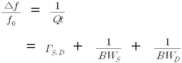
In Equation (1), f0 is the center frequency,

Figure 112010054727987-pat00002
Bandwidth,
Figure 112010054727987-pat00003
BWS is the resonant bandwidth of the source resonator 115, and BWD is the resonant bandwidth of the target resonator 121. [ In this specification, the BW-factor means 1 / BWS or 1 / BWD.

On the other hand, impedance mismatching occurs between the source resonator 115 and the target resonator 121 due to external influences such as a difference between the distance between the source resonator 115 and the target resonator 121, . Impedance mismatching can be a direct cause of reducing the efficiency of power transfer. The matching controller 113 determines that impedance mismatching has occurred by detecting a reflected wave that is reflected by a part of the transmission signal and performs impedance matching. In addition, the matching controller 113 can change the resonance frequency by detecting the resonance point through waveform analysis of the reflected wave. Here, the matching controller 113 can determine the resonance frequency as the frequency with the minimum amplitude in the waveform of the reflected wave.

In the example of FIG. 1, the source resonator 115 and / or the target resonator 121 may have the structure of FIG. 13 to FIG.

2 shows a resonant power transmission system according to one embodiment.

Referring to FIG. 2, the source apparatus of the resonant power transmission system includes an AC / DC converter 210, a DC / AC inverter, and a source resonator unit 230. The target device of the resonant power transmission system also includes a target resonator 240 and an AC / DC converter 250. In the example of FIG. 2, the load 260 may be a configuration included in the target device or an external device.

Referring to FIG. 2, impedance matching for changes in the impedance Z L of the load 260 and impedance matching for changes in the impedance of the source device as viewed from the target device can be performed at point B. In addition, the impedance matching with respect to the impedance change between the DC / AC inverter 220 and the source resonator 230 can be performed at the A point. Here, the impedance matching can be performed through impedance tracking, which will be described later. Hereinafter, impedance tracking in the source device, impedance tracking in the target device, and impedance tracking between the source device and the target device will be described in detail through specific configurations of the source device and the target device.

On the other hand, the resonance impedance tracking device for tracking the resonance impedance may be provided in each of the source device and the target device, or may be provided in either the source device or the target device. Here, the resonance impedance means an impedance value when the resonator has a resonance frequency.

3 shows a configuration of a source apparatus according to an embodiment.

3, the source apparatus 300 includes a voltage control unit 310, an AC / DC inverter 320, a switching control unit 330, a source control unit 340, a target sensing unit 350, 360, and a source resonator 390.

The voltage controller 310 receives the AC signal of the first frequency and outputs a DC voltage of a predetermined level. Here, the first frequency may be, for example, several tens Hz. Here, the AC signal of the first frequency may be generated by a high-speed switching method using a high-speed switching element, or may be generated by an oscillation method using an oscillator. The voltage control unit 310 may include a transformer 311, a rectification unit 313, and a constant voltage control unit 315.

The transformer 311 adjusts the signal level of the AC signal input from the external device to a desired level.

The rectifying unit 313 rectifies an AC signal output from the transformer 311 to output a DC signal.

The constant voltage control unit 315 outputs a DC voltage at a constant level under the control of the source control unit 340. [ The constant voltage control unit 315 may include a stabilization circuit for outputting a DC voltage at a constant level. The voltage level of the DC voltage output from the constant voltage control unit 315 may be determined according to the amount of power required in the target apparatus and the amount of output of the resonance power.

The AC / DC inverter 320 converts the DC signal output from the voltage controller 310 into an AC signal to generate a resonance power. That is, the AC / DC inverter 320 converts a DC voltage of a constant level outputted from the constant voltage controller 315 into an AC voltage by the switching pulse signal of the second frequency. The AC / DC inverter 320 may include a switching element for high-speed switching. At this time, the switching element may be configured to be turned on when the switching pulse signal is "high" and turned off when the switching pulse signal is "Low ".

The switching control unit 330 generates a switching pulse signal and provides the generated switching pulse signal to the AC / DC inverter 320. At this time, the switching pulse signal may be generated by a high-speed switching method or an oscillation method. The high-speed switching scheme can be implemented using a high-speed switching device, for example, a field-effect transistor (FET). The oscillation method can be implemented by an oscillator. That is, the switching control unit 330 may further include an oscillator. Here, the oscillator outputs an AC signal having a predetermined oscillation frequency. The switching pulse signal output from the switching control unit 330 has a second frequency. The switching pulse signal may be a square wave as shown in FIG. Also, the switching pulse signal may be a sine wave. The switching controller 330 can control the duty ratio of the switching pulse signal to 50:50 as shown in FIG. Here, the second frequency may be, for example, several MHz to several tens MHz. The duty ratio of the switching pulse signal may be set to have a margin of 10% based on 50:50. That is, the switching controller 330 can control the duty ratio of the switching pulse signal to 40 to 60%.

The source control 340 may be configured to control the overall operation, impedance matching, and resonant impedance tracking of the source device. Accordingly, the source control unit 340 may include at least one processor. For example, at least one processor included in the source control unit 340 may be configured to control resonant impedance tracking.

The source control unit 340 controls the tracking of the resonance impedance according to whether the impedance of the target device changes or at least one of the reflected signals is detected. At this time, the 'tracking of the resonance impedance' is an impedance adjustment process performed by the source impedance tracking unit 370. The source control unit 340 may obtain the amount of change in the impedance of the target device and control the source impedance tracking unit 370 in consideration of the amount of change in the impedance. At this time, the impedance to the target device means the impedance when looking from point A to point B in Fig. A change in impedance to the target device may be provided from the target sensing unit 350 to the source control unit 340. [

The target sensing unit 350 detects a change in the impedance of the target device. The target detection unit 350 detects the target value of the target in consideration of the AC power amount input from the external power source to the voltage control unit 310, the output power amount of the source resonance unit 380, the magnitude of the reflected power corresponding to the resonance power transmitted to the target device, It is possible to detect a change in the impedance to the device. For example, the target sensing unit 350 may sense a change in the impedance of the target device using the ratio of the amount of power and the amount of reflected power of the resonant power transmitted to the target device.

On the other hand, in the resonant power transmission, the voltage relation in consideration of the impedance between the source resonator and the target resonator can be defined as in Equation (1).

[Equation 1]

Figure 112010054727987-pat00004

In Equation (1), Vi denotes an output voltage on the source side, and Vr denotes a reflection voltage due to impedance mismatching. In Equation 1, the reflection coefficient

Figure 112010054727987-pat00005
Can be defined as Equation (2).

&Quot; (2) "

Figure 112010054727987-pat00006

The source-reflected-signal detecting unit 360 detects a reflected signal corresponding to the resonance power transmitted to the target device. The source reflection signal detection unit 360 may include a coupler for coupling the reflection signal. That is, the source-reflected-signal detecting unit 360 can detect the reflected signal through the coupler. In one aspect, the source control unit 360 may control the switch 379 to terminate the resonant impedance tracking if no reflected signal is detected through the source-reflected-signal detecting unit 360. In addition, the source control unit 360 may control the switch 379 to continue resonant impedance tracking when a reflected signal is detected through the source-reflected-signal detecting unit 360.

The source resonance section 390 includes a source impedance tracking section 370 and a source resonator 380.

The source impedance tracking unit 370 adjusts a factor of the resonance frequency to perform tracking of the resonance impedance. The determinant of the resonance frequency means the C value of the resonance frequency defined by Equation (3). The C value is the capacitor component of the resonator.

&Quot; (3) "

Figure 112010054727987-pat00007

In Equation 3, L is the inductance value of the resonator.

'Tracking resonance impedance' means performing impedance matching by tracking or adjusting the C value of the resonator. The C value of the resonator is the same as the C value of the resonance frequency. The source impedance tracking unit 370 may include a variable capacitor or a plurality of capacitors 371, 373, and 375 for tracking the C value of the resonator. The source impedance tracking unit 370 may further include a switch 379. The switch 379 can adjust the factor of determining the resonance frequency by sequentially switching the plurality of capacitors 371, 373, and 375 according to a control signal input from the source controller 340. That is, the source control unit 340 obtains the amount of change in the impedance of the target device from the target sensing unit 350, and can determine the switching direction of the switch 379 in consideration of the amount of change in the impedance. For example, the control signal may be a signal for switching the switch 379 in the direction in which the C value sequentially decreases, or for switching the switch 379 in the direction in which the C value sequentially increases.

Although not shown in FIG. 3, the source apparatus 300 may further include a communication unit. The communication unit may perform in-band communication for transmitting / receiving data to / from the target device through a resonant frequency, and out-band communication for transmitting / receiving data to / from the target device through an allocated frequency for data communication. In one aspect, the communication unit may receive the impedance change amount of the load sensed by the target device and provide the impedance change amount to the source control unit 340. The source control unit 340 may control the source impedance tracking unit 370 using the impedance variation of the load.

4 shows a configuration of a target device according to an embodiment.

4, the target device 400 includes a target resonance part 450, an AC / DC converter 470, a DC / DC converter 480, a load sensing part 410, a target reflection signal detection part 420, And a target control unit 440. In the example of FIG. 4, the load 401 may be a configuration included in the target device 400 or an external device.

The target resonator portion 450 is configured similarly to the source resonator portion 390. That is, the target resonator 450 includes a target resonator 460 and a target impedance tracking unit 430.

The target impedance tracking unit 430 adjusts a factor of a resonance frequency to perform tracking of a resonance impedance. The tracking of the resonance impedance performed by the target impedance tracking unit 430 is an impedance adjustment process at point B in FIG. The resonant impedance tracking performed in the target impedance tracking unit 430 may be performed in the same manner as that performed in the source impedance tracking unit 370. [ Like the source impedance tracking unit 370, the target impedance tracking unit 430 may include a plurality of capacitors 431, 433, and 435 and a switch 437.

The AC / DC converter 470 converts the AC voltage to a DC voltage. That is, the AC / DC converter 470 can convert the resonance power, which is an AC signal, into DC power.

The DC / DC converter 480 supplies the rated voltage to the load 401 by adjusting the signal level of the DC voltage.

The load sensing unit 410 detects a change in the impedance of the load 401 and the impedance of the load 401 connected to the target device 400 receiving the resonant power. At this time, the load sensing unit 410 can detect a change in the impedance of the load by sensing the voltage applied to the load 401 and the amount of the current flowing to the load 401.

The target reflection signal detector 420 detects a reflection signal corresponding to the received resonance power. The target reflection signal detection unit 420 may include a coupler for coupling the reflection signal. That is, the target reflection signal detector 420 can detect the reflection signal through the coupler. In one aspect, the target control unit 440 may control the switch 437 to terminate the resonant impedance tracking if a reflected signal is not detected through the target reflected signal detecting unit 420. In addition, the target controller 440 may control the switch 437 to continue resonant impedance tracking when a reflected signal is detected through the target reflection signal detector 420. There are many reasons why a reflected signal is generated. For example, even when the consumed power of the load 401 changes, the impedance of the load may change.

The target control 440 may be configured to control the overall operation, impedance matching, and resonant impedance tracking of the target device 400. Accordingly, the target control unit 440 may include at least one processor. For example, at least one processor included in the target controller 440 may be configured to control resonant impedance tracking.

The target control unit 440 can control the tracking of the resonance impedance based on whether or not at least one of the impedance change of the load 401 and the reflected signal is detected. The target control unit 440 may obtain the variation of the impedance of the load and may control the target impedance tracking unit 430 in consideration of the variation of the impedance. The target control unit 440 can control the switching direction of the switch 437 in accordance with the change amount of the impedance of the load. For example, the target control unit 440 can control the switch 437 in a direction in which the C value of the target resonator 460 is sequentially decreased.

Although not shown in FIG. 4, the target device 400 may further include a communication unit. The communication unit may perform in-band communication for transmitting / receiving data with the source device through the resonance frequency, and out-band communication for transmitting / receiving data to / from the source device through the allocated frequency for data communication. In one aspect, the communication unit may transmit to the source device an amount of change in impedance of the load detected by the target device.

7 shows an example in which the target device performs resonant impedance tracking with the source device fixed.

7 is a representation of the impedance Z L of the impedance Z 0 and a load of the source device equivalently. 7,

Figure 112010054727987-pat00008
Quot; means the reflected impedance or reflected power of the target device to the source device.

In the resonant power transmission system, the efficiency U can be defined as: " (4) "

&Quot; (4) "

Figure 112010054727987-pat00009

Where K is the coupling coefficient for the energy coupling between the source resonator and the target resonator,

Figure 112010054727987-pat00010
Is the reflection impedance at the source resonator,
Figure 112010054727987-pat00011
Is the reflection impedance at the target resonator,
Figure 112010054727987-pat00012
Is the resonant frequency, M is the mutual inductance between the resonator and the source target resonator, R S is the source impedance of the resonator, R D is a Q-factor, Q D of the impedance, Q S is the source of the target cavity resonator is a resonator of the target Q- and Q K is the Q-factor for the energy coupling between the source resonator and the target resonator. Referring to Equation (4), when the resonance impedance changes
Figure 112010054727987-pat00013
or
Figure 112010054727987-pat00014
The overall efficiency U can be maintained.

8 shows a method of tracking the resonant impedance of a target device in a state where the source device is fixed. The method shown in Fig. 8 may be performed by the target apparatus 400. Fig.

Referring to FIG. 8, the target device 400 receives the resonant power from the source device in step 810. The resonance power received in step 810 may have a small amount of power enough to wake-up the target control unit 440. [

In operation 820, the target apparatus 400 wakes up or activates the target control unit 440 using the received resonance power.

In step 830, the target device 400 checks the reception state of the resonance power. For example, the target device 400 may check whether the amount of received resonant power is constant, whether the receiving state is unstable, and the like.

The target device 400 detects the impedance of the load in step 840 and detects a change in the impedance of the load in step 850. That is, in step 850, the target device 400 determines whether a change in the impedance of the load is detected. If a change in the impedance of the load is detected, the target device 400 performs tracking of the resonance impedance in step 860.

In step 860, the target device 400 performs tracking of the resonance impedance based on whether the change in the impedance is detected and the amount of change in the impedance. The change amount of the impedance can be detected by detecting the voltage applied to the load and the amount of current flowing to the load.

In step 870, the target device 400 controls the tracking of the resonance impedance based on whether or not the reflected signal corresponding to the resonance power is detected. That is, if the target device 400 detects a reflected signal, the target device 400 returns to step 860 and controls the target impedance tracking unit 430 to continue tracking the resonance impedance. Also, if no reflected signal is detected, the target device 400 may return to step 830 or terminate the resonant impedance tracking method.

Step 870 may include generating a control signal related to a change amount of the impedance of the load, and sequentially changing the determination factor of the resonance frequency based on the control signal. The 'control signal related to the amount of change in impedance' may be a sequence of sequentially changing the determination factors of the resonance frequency. The determining element of the resonant frequency may be the capacitor component of the target resonator. The control signal may be information on a sequential increase or decrease of the capacitor component.

9 shows an example in which the source apparatus performs resonant impedance tracking in accordance with a change in load.

9 is a representation of the impedance Z L of the impedance Z 0 and a load of the source apparatus as shown in FIG equivalently. 9

Figure 112010054727987-pat00015
Quot; refers to the reflective impedance or reflected power of the source device relative to the target device. AC power input to the source device, power conversion loss resulting from conversion to resonant power, and
Figure 112010054727987-pat00016
The source apparatus can know Z L. The source device can perform resonant impedance tracking by detecting changes in Z L.

10 shows a resonant impedance tracking method performed in a source apparatus according to a change in load. The method shown in FIG. 10 may be performed by the source apparatus 300.

Referring to FIG. 10, the source apparatus 300 measures an input AC power input from an external apparatus in step 1010.

In operation 1020, the source device 300 detects the load of the target device. Here, sensing the load of the target device means sensing the magnitude of the impedance Z L for the target device in FIG.

In step 1030, the source device 300 detects a change in impedance to the target device. That is, in step 1030, the source apparatus 300 determines whether a change in the impedance of the target apparatus is detected. When a change in the impedance of the target apparatus is detected, the apparatus performs the resonance impedance tracking in step 1040.

In operation 1040, the source device 300 performs tracking of the resonance impedance based on whether or not a change in the impedance of the target device is detected and the amount of change in the impedance of the target device. Here, a change in the impedance to the target device can be detected based on the amount of power of the resonant power transmitted to the target device and the reflected signal.

In step 1050, the source apparatus 300 controls the tracking of the resonance impedance based on whether or not the reflected signal corresponding to the resonance power is detected. That is, when the reflected signal is detected, the source apparatus 300 returns to step 1040 and controls the source impedance tracking unit 370 to continue tracking the resonance impedance. In addition, if the reflected signal is not detected, the source apparatus 300 may return to step 1010 or terminate the resonance impedance tracking method.

The step 1050 may include generating a control signal related to the amount of change in the impedance of the target device, and sequentially changing the determination factor of the resonance frequency based on the control signal. The 'control signal related to the amount of change in impedance' may be a sequence of sequentially changing the determination factors of the resonance frequency. The determining element of the resonant frequency may be the capacitor component of the target resonator. The control signal may be information on a sequential increase or decrease of the capacitor component.

11 shows a resonant impedance tracking method between a source device and a target device in accordance with a change in load.

When the source device detects the connection of the target device, it first needs to know the magnitude of the load Z L for the target device. The source device transmits Wake-Up Power to the target device in step 1110 to know Z L. Here, Wake-Up Power is a power having a small amount of power such that a processor or the like provided in the target device can be activated.

When the target device is turned on by Wake-Up Power, load detection is performed in step 1120. Load sensing is to sense the magnitude of the impedance of the load and the change in impedance of the load. In step 1130, the target device performs resonant impedance tracking. Once the resonant impedance tracking is complete, the target device may send a Report to the source device indicating that resonant impedance tracking is complete.

When the resonance impedance tracking of the target device is completed, the source device performs resonance impedance tracking in step 1150. When the resonance impedance tracking in the source apparatus is completed, the impedance matching matching power is transmitted from the source apparatus to the target apparatus in step 1160.

12 shows an example of a resonance impedance tracking method.

The example shown in Fig. 12 can be performed by a resonance impedance tracing apparatus provided in the source apparatus. In addition, the example shown in FIG. 12 can be performed by a resonance impedance tracing device provided in the target device. In the following description, it is assumed that the example shown in Fig. 12 is performed by a resonance impedance tracking apparatus provided in the target apparatus.

Referring to FIG. 12, the control signal may be information on the switching direction of the switch. In addition, the control signal may be a signal for controlling on / off for a specific capacitor.

In the example of FIG. 12, each of the plurality of capacitors 1201, 1203, and 1205 may be designed to have different C values corresponding to frequency offsets. In the example of FIG. 12, it is assumed that the C values of each of the plurality of capacitors 1201, 1203, and 1205 are 1201 1203, and 1205, respectively.

For example, suppose that the "reference impedance frequency" F2 is the current resonance frequency. Impedance mismatching can occur if a change in load or power consumption connected to the target device changes. The target control unit generates a control signal for resonant impedance tracking when it detects a change in the load. At this time, the target control unit determines whether the resonance impedance tracking should proceed to the High Band or the Low Band. When the resonant impedance tracking proceeds in the direction of the High Band, the switching of the switches can proceed sequentially from F2 to F4. That is, when the impedance of the load changes and the resonance frequency needs to be adjusted in the High Band direction, the target control unit can control the switch to switch from F2 to F4.

On the other hand, the source resonator and / or the target resonator may be composed of a resonator of a helix coil structure, a resonator of a spiral coil structure, or a meta-structured resonator.

It is already well known, but for the sake of comprehension we describe related terms. All materials have inherent permeability (Mu) and permittivity (epsilon). The permeability means the ratio of the density of magnetic flux generated in a given magnetic field to the density of a magnetic flux in a vacuum. And, the dielectric constant means the ratio of the electric flux density occurring to an electric field given to the material and the density of the electric flux generated in the vacuum to the electric field. The permeability and permittivity determine the propagation constant of the material at a given frequency or wavelength, and the electromagnetic properties of the material are determined by the permeability and permittivity. In particular, the artificially designed material having a permittivity or permeability that does not exist in the natural world is called a meta material, and a meta material can be easily formed even at a very large wavelength or a very low frequency region (that is, It can be put in a resonance state.

13 is a view illustrating a two-dimensional structure resonator according to an embodiment of the present invention.

13, a two-dimensional resonator according to an embodiment of the present invention includes a transmission line including a first signal conductor portion 1311, a second signal conductor portion 1312, and a ground conductor portion 1313, A capacitor 1320, a matching device 1330 and conductors 1341 and 1342.

13, a capacitor 1320 is inserted in series between the first signal conductor portion 1311 and the second signal conductor portion 1312 in the transmission line, so that the electric field is And is trapped in the capacitor 1320. Generally, the transmission line includes at least one conductor at the top and at least one conductor at the bottom, where current flows through the conductor at the top and the conductor at the bottom is electrically grounded. In the present specification, the conductor on the upper portion of the transmission line is referred to as a first signal conductor portion 1311 and the second signal conductor portion 1312, and the conductor under the transmission line is referred to as a ground conductor portion 1313 .

As shown in FIG. 13, the resonator 1300 according to an embodiment of the present invention has a two-dimensional structure. The transmission line includes a first signal conductor portion 1311 and a second signal conductor portion 1312 at an upper portion thereof and a ground conductor portion 1313 at a lower portion thereof. The first signal conductor portion 1311 and the second signal conductor portion 1312 and the ground conductor portion 1313 are disposed facing each other. The current flows through the first signal conductor portion 1311 and the second signal conductor portion 1312.

13, one end of the first signal conductor portion 1311 is shorted to the conductor 1342, and the other end is connected to the capacitor 1320. [ One end of the second signal conductor portion 1312 is grounded to the conductor 1341 and the other end is connected to the capacitor 1320. As a result, the first signal conductor portion 1311, the second signal conductor portion 1312, and the ground conductor portion 1313 and the conductors 1341 and 1342 are connected to each other so that the resonator 1300 has an electrically closed loop structure . Here, the 'loop structure' includes a circular structure, a polygonal structure such as a quadrangle, and the like, and having a loop structure means that it is electrically closed.

The capacitor 1320 is inserted in the middle of the transmission line. More specifically, a capacitor 1320 is inserted between the first signal conductor portion 1311 and the second signal conductor portion 1312. At this time, the capacitor 1320 may have the form of a lumped element and a distributed element. In particular, a dispersed capacitor in the form of a dispersive element can comprise zigzag shaped conductor lines and a dielectric with a high dielectric constant existing between the conductor lines.

As the capacitor 1320 is inserted into the transmission line, the resonator 1300 may have a characteristic of metamaterial. Here, a metamaterial is a material having a special electrical property that can not be found in nature, and has an artificially designed structure. The electromagnetic properties of all materials present in nature have inherent permittivity or permeability, and most materials have a positive permittivity and a positive permeability. In most materials, the right-hand rule applies to electric fields, magnetic fields and pointing vectors, so these materials are called RHM (Right Handed Material). However, the meta-material is a material having a permittivity or permeability that does not exist in the natural world, and may be an epsilon negative material, an MNG (mu negative material), a DNG (double negative) material, index material, left-handed material, and the like.

At this time, when the capacitance of the capacitor 1320 inserted as a lumped element is appropriately determined, the resonator 1300 may have a metamaterial characteristic. In particular, by properly adjusting the capacitance of the capacitor 1320, the resonator can have a negative permeability, so that the resonator 1300 according to one embodiment of the present invention can be referred to as an MNG resonator. As will be described below, the criterion for determining the capacitance of the capacitor 1320 may vary. A criterion that allows the resonator 1300 to have a characteristic of a metamaterial, a premise that the resonator 1300 has a negative permeability at a target frequency or the resonator 1300 is a zero- A presupposition that has a resonance (Zeroth-Order Resonance) characteristic, and the capacitance of the capacitor 1320 can be determined under the premise of at least one of the above-mentioned premises.

The MNG resonator 1300 may have a zeroth-order resonance characteristic having a frequency when the propagation constant is 0 as a resonant frequency. Since the MNG resonator 1300 may have a zero-th resonance characteristic, the resonance frequency may be independent of the physical size of the MNG resonator 1300. That is, as will be described later, it is sufficient to appropriately design the capacitor 1320 in order to change the resonance frequency in the MNG resonator 1300, so that the physical size of the MNG resonator 1300 may not be changed.

In addition, since the electric field in the near field is concentrated in the capacitor 1320 inserted in the transmission line, the magnetic field is dominant in the near field due to the capacitor 1320. Since the MNG resonator 1300 can have a high Q-factor by using the capacitor 1320 of the concentration device, the efficiency of power transmission can be improved. For reference, the queue-factor represents the ratio of the reactance to the degree of resistance or ohmic loss in the wireless power transmission, the larger the queue-factor, the greater the efficiency of the wireless power transmission .

In addition, the MNG resonator 1300 may include a matching unit 1330 for impedance matching. At this time, the matching unit 1330 appropriately tunes the intensity of the magnetic field of the MNG resonator 1300, and the impedance of the MNG resonator 1300 is determined by the matching unit 1330. The current may then flow into the MNG resonator 1300 through the connector 1340 or out of the MNG resonator 1300. Here, the connector 1340 may be connected to the ground conductor portion 1313 or the matching unit 1330. A physical connection may be formed between the connector 1340 and the ground conductor portion 1313 or the matching device 1330 and a physical connection between the connector 1340 and the ground conductor portion 1313 or the matching device 1330. [ Power may be delivered through the coupling without any connection.

More specifically, as shown in FIG. 13, the matching unit 1330 may be located inside a loop formed by the loop structure of the resonator 1300. The matching device 1330 can adjust the impedance of the resonator 1300 by changing the physical shape. In particular, the matching device 1330 may include a conductor 1331 for impedance matching at a distance h from the ground conductor portion 1313 and the impedance of the resonator 1300 may be varied by adjusting the distance h have.

13, if there is a controller capable of controlling the matching machine 1330, the matching machine 1330 may change the physical form of the matching machine 1330 according to the control signal generated by the controller have. For example, the distance h between the conductor 1331 and the ground conductor portion 1313 of the matching device 1330 may be increased or decreased depending on the control signal, so that the physical form of the matching device 1330 may be changed The impedance of the resonator 1300 can be adjusted. The controller can generate control signals in consideration of various factors, which will be described below.

Matcher 1330 may be implemented as a passive element, such as conductor portion 1331, as shown in FIG. 13, and may be implemented as an active element such as a diode, transistor, or the like, depending on the embodiment. When the active element is included in the matching device 1330, the active element can be driven according to the control signal generated by the controller, and the impedance of the resonator 1300 can be adjusted according to the control signal. For example, the matching device 1330 may include a diode that is a kind of active device, and the impedance of the resonator 1300 may be adjusted depending on whether the diode is in an 'on' state or an 'off' state .

Though not shown in FIG. 13, a magnetic core passing through the MNG resonator 1300 may further be included. Such a magnetic core can perform a function of increasing a power transmission distance.

14 is a view showing a three-dimensional resonator according to an embodiment of the present invention.

14, a three-dimensional resonator 1300 according to an embodiment of the present invention includes a first signal conductor portion 1311, a second signal conductor portion 1312, and a ground conductor portion 1313 A transmission line and a capacitor 1320. Where the capacitor 1320 is inserted in series between the first signal conductor portion 1311 and the second signal conductor portion 1312 in the transmission line and the electric field is trapped in the capacitor 1320.

Also, as shown in Fig. 14, the resonator 1300 has a three-dimensional structure. The transmission line includes a first signal conductor portion 1311 and a second signal conductor portion 1312 at an upper portion thereof and a ground conductor portion 1313 at a lower portion thereof. The first signal conductor portion 1311 and the second signal conductor portion 1312 and the ground conductor portion 1313 are disposed facing each other. Current flows in the x direction through the first signal conductor portion 1311 and the second signal conductor portion 1312, and the magnetic field H (w) is generated in the -y direction due to this current. Of course, a magnetic field H (w) may occur in the + y direction, unlike that shown in FIG.

14, one end of the first signal conductor portion 1311 is shorted to the conductor 1342, and the other end is connected to the capacitor 1320. [ One end of the second signal conductor portion 1312 is grounded to the conductor 1341 and the other end is connected to the capacitor 1320. As a result, the first signal conductor portion 1311, the second signal conductor portion 1312, and the ground conductor portion 1313 and the conductors 1341 and 1342 are connected to each other so that the resonator 1300 has an electrically closed loop structure . Here, the 'loop structure' includes a circular structure, a polygonal structure such as a quadrangle, and the like, and having a loop structure means that it is electrically closed.

In addition, capacitor 1320 is inserted between first signal conductor portion 1311 and second signal conductor portion 1312, as shown in Fig. At this time, the capacitor 1320 may have the form of a lumped element and a distributed element. In particular, a dispersed capacitor in the form of a dispersive element can comprise zigzag shaped conductor lines and a dielectric with a high dielectric constant existing between the conductor lines.

As shown in FIG. 14, as the capacitor 1320 is inserted into the transmission line, the resonator 1300 may have a characteristic of metamaterial. When the capacitance of the capacitor 1320 inserted as a lumped element is appropriately determined, the resonator 1300 may have the property of a metamaterial. In particular, by appropriately adjusting the capacitance of the capacitor 1320, the resonator 1300 can have a negative permeability in a certain frequency band, so that the resonator 1300 according to an embodiment of the present invention can be referred to as an MNG resonator. As will be described below, the criterion for determining the capacitance of the capacitor 1320 may vary. A criterion that allows the resonator 1300 to have a characteristic of a metamaterial, a premise that the resonator 1300 has a negative permeability at a target frequency or the resonator 1300 is a zero- A presupposition that has a resonance (Zeroth-Order Resonance) characteristic, and the capacitance of the capacitor 1320 can be determined under the premise of at least one of the above-mentioned premises.

The MNG resonator 1300 shown in FIG. 14 may have a zeroth-order resonance characteristic having a resonance frequency at a frequency when the propagation constant is zero. Since the MNG resonator 1300 may have a zero-th resonance characteristic, the resonance frequency may be independent of the physical size of the MNG resonator 1300. In order to change the resonance frequency in the MNG resonator 1300, it is sufficient to appropriately design the capacitor 1320, so that the physical size of the MNG resonator 1300 may not be changed.

Referring to the MNG resonator 1300 as shown in FIG. 14, since the electric field in the near field is concentrated in the capacitor 1320 inserted in the transmission line 1310, the capacitor 1320 causes the near field The magnetic field becomes dominant. In particular, since the MNG resonator 1300 having zeroth-order resonance characteristics has characteristics similar to those of a magnetic dipole, the magnetic field is dominant in the near field and is generated due to the insertion of the capacitor 1320 A small amount of electric field is also concentrated in the capacitor 1320, so that the magnetic field becomes even more dominant in the near field. The MNG resonator 1300 can have a high Q-factor using the capacitor 1320 of the lumped element, thereby improving the efficiency of power transmission.

In addition, the MNG resonator 1300 shown in FIG. 14 may include a matching unit 1330 for impedance matching. At this time, the matching unit 1330 appropriately tunes the intensity of the magnetic field of the MNG resonator 1300, and the impedance of the MNG resonator 1300 is determined by the matching unit 1330. Then, current flows into the MNG resonator 1300 through the connector 1340 or flows out from the MNG resonator 1300. Here, the connector 1340 may be connected to the ground conductor portion 1313 or the matching unit 1330.

More specifically, as shown in FIG. 14, the matching unit 1330 may be located inside a loop formed by the loop structure of the resonator 1300. The matching device 1330 can adjust the impedance of the resonator 1300 by changing the physical shape. In particular, the matching device 1330 may include a conductor portion 1331 for impedance matching at a distance h from the ground conductor portion 1313 and the impedance of the resonator 1300 may be varied by adjusting the distance h .

Although not shown in FIG. 14, when there is a controller capable of controlling the matching machine 1330, the matching machine 1330 can change the physical form of the matching machine 1330 according to a control signal generated by the controller have. For example, the distance h between the conductor 1331 and the ground conductor portion 1330 of the matching device 1330 may be increased or decreased depending on the control signal, so that the physical form of the matching device 1330 may be changed The impedance of the resonator 1300 can be adjusted. The distance h between the conductor 1331 of the matching device 1330 and the ground conductor portion 1330 can be adjusted in various manners. That is, first, the matching unit 1330 may include several conductors, and the distance h may be adjusted by adaptively activating any one of the conductors. Second, by adjusting the physical position of the conductor 1331 up and down, the distance h can be adjusted. This distance h can be controlled according to the control signal of the controller, and the controller can generate the control signal considering various factors. The generation of the control signal by the controller will be described below.

Matcher 1330 may be implemented as a passive element, such as conductor portion 1331, as shown in FIG. 14, and may be implemented as an active element such as a diode, transistor, or the like, depending on the embodiment. When the active element is included in the matching device 1330, the active element can be driven according to the control signal generated by the controller, and the impedance of the resonator 1300 can be adjusted according to the control signal. For example, the matching device 1330 may include a diode that is a kind of active device, and the impedance of the resonator 1300 may be adjusted depending on whether the diode is in an 'on' state or an 'off' state .

Further, although not explicitly shown in FIG. 14, a magnetic core passing through the MNG resonator 1300 may be further included. Such a magnetic core can perform a function of increasing a power transmission distance.

Fig. 15 is a view showing an example of a resonator for a wireless power transmission designed in a bulky type.

Referring to FIG. 15, the first signal conductor portion 1311 and the conductor 1342 may be fabricated separately and then integrally formed instead of being connected to each other. Likewise, the second signal conductor portion 1312 and the conductor 1341 can also be fabricated as a single unit.

If the second signal conductor portion 1312 and the conductor 1341 are separately fabricated and then connected together, there may be a conductor loss due to the seam 1350. According to the embodiment of the present invention, the second signal conductor portion 1312 and the conductor 1341 are connected to each other seamlessly, and the conductor 1341 and the ground conductor portion 1313 are also separated from each other Can be connected to each other seamlessly, and the conductor loss due to the joint can be reduced. As a result, the second signal conductor portion 1312 and the ground conductor portion 1313 can be fabricated as a single unit without separate seams. Likewise, the first signal conductor portion 1311 and the ground conductor portion 1313 can be fabricated as a single unit without separate seams.

As shown in FIG. 15, a type that connects two or more partitions together as one integral type without separate seam is called a 'bulky type'.

16 is a view showing an example of a resonator for wireless power transmission designed as a hollow type.

16, the first signal conductor portion 1311, the second signal conductor portion 1312, the ground conductor portion 1313, and the conductors 1341 and 1342 of the resonator for radio power transmission designed as a hollow type Includes an empty space inside.

At a given resonant frequency, the effective current flows through all portions of each of the first signal conductor portion 1311, the second signal conductor portion 1312, the ground conductor portion 1313, and the conductors 1341 and 1342 But can be modeled as flowing through only a portion of the portion. That is, at a given resonant frequency, the thickness of the first signal conductor portion 1311, the second signal conductor portion 1312, the ground conductor portion 1313, and the conductors 1341 and 1342 exceeds the respective skin depths Thick ones can be inefficient. That is, it may cause the weight of the resonator 1300 or the manufacturing cost of the resonator 1300 to increase.

Therefore, according to the embodiment of the present invention, the skin depth of each of the first signal conductor portion 1311, the second signal conductor portion 1312, the ground conductor portion 1313, and the conductors 1341 and 1342 at a given resonance frequency The thicknesses of the first signal conductor portion 1311, the second signal conductor portion 1312, the ground conductor portion 1313, and the conductors 1341 and 1342 can be appropriately determined based on the thickness of the first signal conductor portion 1311, the second signal conductor portion 1312, If each of the first signal conductor portion 1311, the second signal conductor portion 1312, the ground conductor portion 1313 and the conductors 1341 and 1342 has a thickness greater than the corresponding skin depth but has an appropriate thickness, And the fabrication cost of the resonator 1300 can also be reduced.

For example, as shown in FIG. 16, the thickness of the second signal conductor portion 1312 can be defined as dm, and d

Figure 112010054727987-pat00017
Lt; / RTI > Where f is the frequency,
Figure 112010054727987-pat00018
Is the investment rate,
Figure 112010054727987-pat00019
Represents a conductor constant. Particularly, the first signal conductor portion 1311, the second signal conductor portion 1312, the ground conductor portion 1313, and the conductors 1341 and 1342 are made of copper and have a conductivity of 5.8x10 < , The skin depth may be about 0.6 mm for the resonance frequency of 10 kHz and the skin depth may be 0.006 mm for the resonance frequency of 100 MHz.

17 is a view showing an example of a resonator for wireless power transmission to which a parallel-sheet is applied.

Referring to FIG. 17, a parallel-sheet may be applied to the surfaces of the first signal conductor portion 1311 and the second signal conductor portion 1312 included in the resonator for the wireless power transmission to which the parallel-sheet is applied.

Since the first signal conductor portion 1311 and the second signal conductor portion 1312 are not perfect conductors, they may have resistance components, and ohmic losses may occur due to their resistance components . This resistance loss can reduce the Q factor and reduce the coupling efficiency.

According to an embodiment of the present invention, applying a parallel-sheet to the surface of each of the first signal conductor portion 1311 and the second signal conductor portion 1312 reduces resistance loss and increases the Q factor and coupling efficiency . Referring to portion 1370 of FIG. 17, when a parallel-sheet is applied, each of the first signal conductor portion 1311 and the second signal conductor portion 1312 includes a plurality of conductor lines. These conductor lines are arranged in parallel and shorted at the ends of the first signal conductor portion 1311 and the second signal conductor portion 1312, respectively.

When parallel-sheet is applied to the surface of each of the first signal conductor portion 1311 and the second signal conductor portion 1312, the sum of the resistance components of the conductor lines is reduced because the conductor lines are arranged in parallel. Thus, the resistance loss can be reduced, and the Q factor and coupling efficiency can be increased.

18 is a diagram illustrating an example of a resonator for wireless power transmission including a distributed capacitor.

Referring to FIG. 18, the capacitor 1320 included in the resonator for wireless power transmission may be a distributed capacitor. The capacitor as a lumped element may have a relatively high Equivalent Series Resistance (ESR). Although there are various proposals for reducing the ESR of a capacitor as a concentration device, the embodiment of the present invention can reduce the ESR by using the capacitor 1320 as a dispersion element. For reference, loss due to ESR can reduce Q factor and coupling efficiency.

The capacitor 1320 as a dispersion element may have a zigzag structure as shown in Fig. That is, the capacitor 1320 as a dispersion element can be realized by a conductor line and a dielectric of a zigzag structure.

In addition, as shown in FIG. 18, the embodiment of the present invention uses a capacitor 1320 as a dispersing element, so that loss due to ESR can be reduced, and capacitors as a plurality of lumped elements can be used in parallel The loss due to the ESR can be reduced. Because the resistance components of each of the capacitors as the lumped element are reduced through the parallel connection, the effective resistance of the capacitors as the lumped elements connected in parallel can also be reduced, and thus the loss due to the ESR can be reduced. For example, replacing the use of one 10 pF capacitor with the use of ten 1 pF capacitors can reduce losses due to ESR.

19 is a diagram showing examples of matching devices used in a two-dimensional resonator and a three-dimensional resonator.

Fig. 19A shows a part of the two-dimensional resonator shown in Fig. 13 including the matching unit, and B in Fig. 19 shows a part of the three-dimensional resonator shown in Fig. 14 including the matching unit.

19A, the matching unit includes a conductor 1331, a conductor 1332, and a conductor 1333, and the conductor 1332 and the conductor 1333 are connected to the ground conductor portion 1313 and the conductor 1331). The impedance of the two-dimensional resonator is determined according to the distance h between the conductor 1331 and the ground conductor portion 1313 and the distance h between the conductor 1331 and the ground conductor portion 1313 is controlled by the controller. The distance h between the conductor 1331 and the ground conductor portion 1313 can be adjusted in various manners and can be adjusted by adjusting the distance h by adaptively activating any of the various conductors that may be conductors 1331 And a method of adjusting the distance h by adjusting the physical position of the conductor 1331 up and down.

19B, the matching unit includes a conductor 1331, a conductor 1332, and a conductor 1333, and the conductor 1332 and the conductor 1333 include a ground conductor portion 1313 and a conductor 1333 of the transmission line. 1331). The impedance of the three-dimensional resonator is determined according to the distance h between the conductor 1331 and the ground conductor portion 1313 and the distance h between the conductor 1331 and the ground conductor portion 1313 is controlled by the controller. The distance h between the conductor 1331 and the ground conductor portion 1313 can be adjusted in various ways in the matching device included in the three-dimensional resonator as well as the matching device included in the two-dimensional resonator. For example, the distance h may be adjusted by adaptively activating any one of the conductors that may be the conductor 1331, and the distance h may be adjusted by vertically adjusting the physical position of the conductor 1331 Method, and the like.

Although not shown in FIG. 19, the matching unit may include an active element, and the method of adjusting the impedance of the resonator using the active element is similar to that described above. That is, by changing the path of the current flowing through the matching device using the active element, the impedance of the resonator can be adjusted.

Fig. 20 is a diagram showing an equivalent circuit of the resonator for wireless power transmission shown in Fig. 13. Fig.

The resonator for the wireless power transmission shown in Fig. 13 can be modeled as the equivalent circuit shown in Fig. In the equivalent circuit of Fig. 20, C L represents a capacitor inserted in the form of a lumped element in the middle of the transmission line of Fig.

At this time, the resonator for the radio power transmission shown in Fig. 13 has the zero-th resonance characteristic. That is, when the propagation constant is zero, the resonator for wireless power transmission

Figure 112010054727987-pat00020
Is assumed to have a resonant frequency. At this time,
Figure 112010054727987-pat00021
Can be expressed by the following equation (1). Here, MZR means Mu Zero Resonator.

[Equation 1]

Figure 112010054727987-pat00022

Referring to Equation 1, the resonance frequency of the resonator

Figure 112010054727987-pat00023
The
Figure 112010054727987-pat00024
And the resonance frequency < RTI ID = 0.0 >
Figure 112010054727987-pat00025
And the physical size of the resonator can be independent of each other. Therefore,
Figure 112010054727987-pat00026
And the physical size of the resonator are independent of each other, the physical size of the resonator can be sufficiently small.

On the other hand, although not explicitly shown in FIG. 13, the capacitor 1420 may be connected to the source impedance tracking portion 370 of FIG. 3 or the target impedance tracking portion 430 of FIG. For example, the capacitor 1420 may be connected in parallel with the capacitor 431. That is, the source impedance tracking unit 370 or the target impedance tracking unit 430 of FIG. 4 may be connected to the capacitor 1420 in various forms to adjust the C L value of the resonator 1300.

The methods according to embodiments of the present invention may be implemented in the form of program instructions that can be executed through various computer means and recorded in a computer-readable medium. The computer-readable medium may include program instructions, data files, data structures, and the like, alone or in combination. The program instructions recorded on the medium may be those specially designed and configured for the present invention or may be available to those skilled in the art of computer software.

While the invention has been shown and described with reference to certain preferred embodiments thereof, it will be understood by those of ordinary skill in the art that various changes in form and details may be made therein without departing from the spirit and scope of the invention as defined by the appended claims. This is possible.

Therefore, the scope of the present invention should not be limited to the described embodiments, but should be determined by the equivalents of the claims, as well as the claims.

Claims (18)

A load sensing unit for sensing an impedance of a load connected to a target device receiving the resonance power transmitted by the source device and a change in the impedance of the load;
A target reflection signal detector for detecting a reflection signal corresponding to the resonance power;
A target impedance tracking unit that adjusts a factor of a resonance frequency to perform tracking of a resonance impedance;
A target control unit for controlling tracking of the resonance impedance based on whether the impedance of the load changes or at least one of the reflection signals is detected; And
A communication unit for transmitting a change amount of the impedance of the load detected by the target device to the source device so that the source device controls the resonance frequency of the source resonator;
Wherein the resonant impedance tracking device comprises:
The method according to claim 1,
The load sensing unit may include:
Detecting a change in the impedance of the load by detecting a voltage applied to the load and an amount of current flowing to the load,
A resonant impedance tracking device in a resonant power delivery system.
The method according to claim 1,
Wherein the target reflected signal detecting unit comprises:
Detecting the reflected signal through a coupler,
A resonant impedance tracking device in a resonant power delivery system.
The method according to claim 1,
Wherein the target impedance tracking unit comprises:
A plurality of capacitors and a switch, wherein the plurality of capacitors are sequentially switched to adjust a determination factor of the resonance frequency,
A resonant impedance tracking device in a resonant power delivery system.
5. The method of claim 4,
Wherein the target control unit comprises:
Wherein the impedance of the load is determined based on a change in impedance of the load,
A resonant impedance tracking device in a resonant power delivery system.
A source-reflected-signal detecting unit that detects a reflected signal corresponding to the resonant power transmitted from the source apparatus to the target apparatus;
A target sensing unit for sensing a change in impedance of the target device;
A source impedance tracking unit that adjusts a factor of a resonance frequency to perform tracking of a resonance impedance;
A source control unit for controlling tracking of the resonance impedance according to whether a change in impedance to the target device or at least one of the reflection signals is detected; And
A communication unit that receives a variation amount of the impedance of the load detected by the target device from the target device and supplies the variation amount of the impedance of the load to the source control unit at all times to control the tracking of the resonance impedance;
Wherein the resonant impedance tracking device comprises:
The method according to claim 6,
Wherein the source reflected signal detecting unit comprises:
Detecting the reflected signal through a coupler,
A resonant impedance tracking device in a resonant power delivery system.
The method according to claim 6,
The target sensing unit may include:
And a control unit for detecting a change in impedance of the target device based on the amount of power of the resonant power transmitted to the target device and the reflected signal,
A resonant impedance tracking device in a resonant power delivery system.
The method according to claim 6,
The source impedance tracking unit,
A plurality of capacitors and a switch, wherein the plurality of capacitors are sequentially switched to adjust a determination factor of the resonance frequency,
A resonant impedance tracking device in a resonant power delivery system.
10. The method of claim 9,
The source control unit,
Obtaining a change amount of an impedance for the target device, and determining a switching direction of the switch in consideration of a change amount of the impedance,
A resonant impedance tracking device in a resonant power delivery system.
A method of tracking a resonant impedance of a target device in a resonant power delivery system,
Detecting a change in the impedance of the load and the impedance of the load connected to the target device receiving the resonant power transmitted by the source device;
Performing tracking of the resonance impedance based on whether the change in the impedance is detected and the amount of change in the impedance;
Controlling tracking of the resonance impedance based on whether or not a reflected signal corresponding to the resonance power is detected; And
Transmitting a change amount of the impedance of the detected load in the target device to the source device so that the source device controls the resonance frequency of the source resonator using the variation amount of the impedance of the load detected in the target device
/ RTI > of claim < RTI ID = 0.0 > 1, < / RTI >
12. The method of claim 11,
The step of detecting a change in the impedance of the load includes:
Detecting a change in the impedance of the load by detecting a voltage applied to the load and an amount of current flowing to the load,
A method of tracking a resonant impedance of a target device.
12. The method of claim 11,
Wherein performing the tracking of the resonant impedance comprises:
Generating a control signal related to an amount of change of the impedance; And
And sequentially changing the determination element of the resonance frequency based on the control signal.
A method of tracking a resonant impedance of a target device.
14. The method of claim 13,
Wherein the determining element of the resonant frequency is a capacitor component of a target resonator and the control signal is information on a sequential increase or decrease of the capacitor component.
A method of tracking a resonant impedance of a target device.
A method of tracking a resonant impedance of a source device in a resonant power delivery system,
Detecting a change in impedance to a target device receiving the resonant power;
Performing tracking of the resonance impedance based on whether or not a change in the impedance of the target device is detected and an amount of change in impedance of the target device; And
Controlling tracking of the resonance impedance based on whether or not a reflected signal corresponding to the resonance power is detected; And
Receiving a change amount of the impedance of the detected load from the target device so as to control the resonance frequency of the source resonator using the variation amount of the impedance of the load detected by the target device
/ RTI > wherein the resonant impedance of the source device is substantially equal to the resonant impedance of the source device.
16. The method of claim 15,
Wherein the change in impedance to the target device is determined based on the amount of power of the resonant power transmitted to the target device and the amount of power,
A method for tracking a resonant impedance of a source device.
16. The method of claim 15,
Wherein performing the tracking of the resonant impedance comprises:
Generating a control signal related to an amount of change of the impedance; And
And sequentially changing the determination element of the resonance frequency based on the control signal.
A method for tracking a resonant impedance of a source device.
18. The method of claim 17,
Wherein the determining element of the resonant frequency is a capacitor component of a source resonator and the control signal is information on a sequential increase or decrease of the capacitor component.
A method for tracking a resonant impedance of a source device.
KR1020100082235A 2010-08-25 2010-08-25 Method and apparatus of tracking of resonance impedance in resonance power transfer system KR101726195B1 (en)

Priority Applications (6)

Application Number Priority Date Filing Date Title
KR1020100082235A KR101726195B1 (en) 2010-08-25 2010-08-25 Method and apparatus of tracking of resonance impedance in resonance power transfer system
US13/210,717 US8704534B2 (en) 2010-08-25 2011-08-16 Method and apparatus of tracking of resonant impedance in resonance power transfer system
EP11820143.3A EP2609666A4 (en) 2010-08-25 2011-08-19 Method and apparatus of tracking of resonant impedance in resonance power transfer system
PCT/KR2011/006142 WO2012026716A2 (en) 2010-08-25 2011-08-19 Method and apparatus of tracking of resonant impedance in resonance power transfer system
JP2013525816A JP5883448B2 (en) 2010-08-25 2011-08-19 Resonance impedance tracking apparatus and method for resonant power transmission system
CN201180033401.1A CN102971940B (en) 2010-08-25 2011-08-19 The method and apparatus of resonance impedance is followed the tracks of in resonance power transfer system

Applications Claiming Priority (1)

Application Number Priority Date Filing Date Title
KR1020100082235A KR101726195B1 (en) 2010-08-25 2010-08-25 Method and apparatus of tracking of resonance impedance in resonance power transfer system

Publications (2)

Publication Number Publication Date
KR20120019090A KR20120019090A (en) 2012-03-06
KR101726195B1 true KR101726195B1 (en) 2017-04-13

Family

ID=45696294

Family Applications (1)

Application Number Title Priority Date Filing Date
KR1020100082235A KR101726195B1 (en) 2010-08-25 2010-08-25 Method and apparatus of tracking of resonance impedance in resonance power transfer system

Country Status (6)

Country Link
US (1) US8704534B2 (en)
EP (1) EP2609666A4 (en)
JP (1) JP5883448B2 (en)
KR (1) KR101726195B1 (en)
CN (1) CN102971940B (en)
WO (1) WO2012026716A2 (en)

Families Citing this family (32)

* Cited by examiner, † Cited by third party
Publication number Priority date Publication date Assignee Title
KR101439350B1 (en) * 2009-07-06 2014-09-15 삼성전자주식회사 Wireless power transmission system and resonator for the system
KR101739283B1 (en) * 2010-08-31 2017-05-25 삼성전자주식회사 Apparatus for adaptive resonant power transmission
JP5674013B2 (en) * 2010-10-08 2015-02-18 ソニー株式会社 Power supply device and power supply system
TWI587597B (en) * 2012-02-17 2017-06-11 Lg伊諾特股份有限公司 Wireless power transmitter, wireless power receiver, and power transmission method of wireless power transmitting system
US20130257167A1 (en) * 2012-03-29 2013-10-03 Integrated Device Technology, Inc. Apparatuses, systems, and methods for power transfer adjustment in wireless power transfer systems
KR101844422B1 (en) 2012-04-19 2018-04-03 삼성전자주식회사 Apparatus and method for wireless energy transmission and apparatus wireless energy reception
KR102023548B1 (en) * 2012-07-10 2019-11-04 삼성전자주식회사 Wireless power transmitter, wireless power receiver and method for controlling each thereof
US9679695B2 (en) * 2012-07-16 2017-06-13 Qualcomm Incorporated Tuning circuit and method for wireless power transfer systems
KR101601352B1 (en) * 2012-09-26 2016-03-08 엘지이노텍 주식회사 Apparatus for transmitting wireless power and method for controlling power thereof
KR101508817B1 (en) * 2012-10-29 2015-04-08 삼성에스디에스 주식회사 System and method for aligning genome sequence
US9543790B2 (en) * 2013-01-24 2017-01-10 Electronics And Telecommunications Research Institute Apparatus for transmitting magnetic resonance wireless power using higher order mode resonance, receiving terminal, and method for transmitting and receiving wireless power using the same
KR102042103B1 (en) * 2013-01-24 2019-11-07 한국전자통신연구원 Apparatus of magnetic resonance using wireless power transmission using higher order mode resonance and receiving terminal thereof, method for transmitting and receiving wireless power by using the same
US9352661B2 (en) * 2013-04-29 2016-05-31 Qualcomm Incorporated Induction power transfer system with coupling and reactance selection
KR101943082B1 (en) * 2014-01-23 2019-04-18 한국전자통신연구원 Wireless power transmission device, wireless power receiving device and wireless power transmission system
KR102187437B1 (en) * 2014-03-11 2020-12-08 엘지이노텍 주식회사 Wireless Power Transfer System including Wireless Power Transfer System-Charger
US9923382B2 (en) * 2014-05-30 2018-03-20 Infineon Technologies Austria Ag Active rectifier for efficient wireless power transfer
CN104659930B (en) * 2014-08-13 2016-05-11 武汉泰可电气股份有限公司 Radio energy receiving equipment and the method for adaptive frequency
CN104578453A (en) * 2015-01-13 2015-04-29 华南理工大学 Magnetic coupling resonance wireless power transmission device achieving self-optimization of frequency and dynamic tuning
CN104682575B (en) * 2015-03-01 2018-01-05 华南理工大学 A kind of resonance type wireless electric energy transmission system for adding both-end impedance transformer network
CN104682576B (en) * 2015-03-01 2017-08-29 华南理工大学 Add the resonance type wireless electric energy transmission system of adaptive both-end impedance transformer network
US10112495B2 (en) 2015-07-27 2018-10-30 Ford Global Technologies, Llc Vehicle wireless charging system including an inverter to control a voltage input to a vehicle power converter
CN106936224B (en) * 2015-12-31 2020-08-25 比亚迪股份有限公司 Wireless charging method and device
KR101846954B1 (en) * 2016-06-13 2018-04-10 주식회사 맵스 Wireless power transmitting unit capable auto-tunning in response to impedance variance of load
KR102018268B1 (en) * 2016-10-18 2019-11-14 엘지이노텍 주식회사 Inductance Mapping Method and Apparatus for Wireless Charging
KR101983802B1 (en) * 2017-11-14 2019-09-03 국방과학연구소 Apparatus for measuring permittivity of doping layer using meta-material, Method thereof, and Computer readable storage medium having the method
KR102092445B1 (en) * 2017-12-12 2020-03-23 한국과학기술원 Powerless electromagnetic sensor and surgical navigation system comprising the same
EP3818620A4 (en) * 2018-07-19 2022-03-23 MediaTek Singapore Pte. Ltd. Detecting foreign objects in wireless power transfer systems
CN109217496B (en) * 2018-10-10 2021-12-07 武汉理工大学 Parameter analysis method for bilateral LCC compensation circuit in wireless electric energy transmission system
JP7211038B2 (en) * 2018-11-29 2023-01-24 株式会社デンソー Defect detection device
JP7211037B2 (en) * 2018-11-29 2023-01-24 株式会社デンソー Signal supply device
GB201820840D0 (en) * 2018-12-20 2019-02-06 Metaboards Ltd Load localisation
WO2020231330A1 (en) * 2019-05-15 2020-11-19 National University Of Singapore Impedance tuning device and method and rectifier circuit, for a wireless power transfer apparatus

Citations (2)

* Cited by examiner, † Cited by third party
Publication number Priority date Publication date Assignee Title
WO2009140220A1 (en) * 2008-05-13 2009-11-19 Qualcomm Incorporated Method and apparatus for adaptive tuning of wireless power transfer
JP2010119515A (en) * 2008-11-18 2010-06-03 Olympus Corp Capsule type medical device

Family Cites Families (18)

* Cited by examiner, † Cited by third party
Publication number Priority date Publication date Assignee Title
GB2197107B (en) 1986-11-03 1990-12-12 Mars Inc Data-storing devices
JP3804334B2 (en) 1999-04-15 2006-08-02 松下電工株式会社 Power supply device and discharge lamp lighting device
US7212414B2 (en) * 1999-06-21 2007-05-01 Access Business Group International, Llc Adaptive inductive power supply
JP4240783B2 (en) 2000-08-28 2009-03-18 パナソニック電工株式会社 Non-contact power transmission device
US6571184B2 (en) 2001-02-06 2003-05-27 Sun Microsystems, Inc. System and method for determining the decoupling capacitors for power distribution systems with a frequency-dependent target impedance
JP4172327B2 (en) * 2003-05-28 2008-10-29 松下電器産業株式会社 Non-contact IC card read / write device and adjustment method thereof
JP2007336788A (en) 2006-06-19 2007-12-27 Dainippon Printing Co Ltd Contactless power supply system, power supply device, and power receiving device
US9129741B2 (en) 2006-09-14 2015-09-08 Qualcomm Incorporated Method and apparatus for wireless power transmission
KR101536367B1 (en) 2007-01-02 2015-07-13 액세스 비지니스 그룹 인터내셔날 엘엘씨 Inductive power supply with device identification
US9124120B2 (en) 2007-06-11 2015-09-01 Qualcomm Incorporated Wireless power system and proximity effects
JP4974171B2 (en) * 2007-12-07 2012-07-11 ソニーモバイルコミュニケーションズ株式会社 Non-contact wireless communication device, method for adjusting resonance frequency of non-contact wireless communication antenna, and portable terminal device
JP2009278837A (en) 2008-05-18 2009-11-26 Hideo Kikuchi Induced-power transmission system
JP4557049B2 (en) * 2008-06-09 2010-10-06 ソニー株式会社 Transmission system, power supply apparatus, power reception apparatus, and transmission method
US20100045114A1 (en) 2008-08-20 2010-02-25 Sample Alanson P Adaptive wireless power transfer apparatus and method thereof
JP5114372B2 (en) * 2008-12-09 2013-01-09 株式会社豊田自動織機 Power transmission method and non-contact power transmission apparatus in non-contact power transmission apparatus
JP5114371B2 (en) * 2008-12-09 2013-01-09 株式会社豊田自動織機 Non-contact power transmission device
JP5349069B2 (en) * 2009-02-09 2013-11-20 株式会社豊田自動織機 Non-contact power transmission device
US8909966B2 (en) * 2010-03-26 2014-12-09 Advantest Corporation Wireless power supply apparatus

Patent Citations (2)

* Cited by examiner, † Cited by third party
Publication number Priority date Publication date Assignee Title
WO2009140220A1 (en) * 2008-05-13 2009-11-19 Qualcomm Incorporated Method and apparatus for adaptive tuning of wireless power transfer
JP2010119515A (en) * 2008-11-18 2010-06-03 Olympus Corp Capsule type medical device

Also Published As

Publication number Publication date
EP2609666A4 (en) 2017-03-01
EP2609666A2 (en) 2013-07-03
CN102971940B (en) 2016-04-13
WO2012026716A3 (en) 2012-05-03
US8704534B2 (en) 2014-04-22
JP2013536671A (en) 2013-09-19
WO2012026716A2 (en) 2012-03-01
US20120049861A1 (en) 2012-03-01
CN102971940A (en) 2013-03-13
JP5883448B2 (en) 2016-03-15
KR20120019090A (en) 2012-03-06

Similar Documents

Publication Publication Date Title
KR101726195B1 (en) Method and apparatus of tracking of resonance impedance in resonance power transfer system
KR101739283B1 (en) Apparatus for adaptive resonant power transmission
KR101859191B1 (en) Method and apparatus for controlling wireless power transmission and reception, and wireless power transmission system
KR101813131B1 (en) Wireless power transmission system and method for controlling of resonance frequency and resonance impedance of wireless power transmission system
KR101358280B1 (en) Method and Apparatus
KR101313662B1 (en) Active rectifier with delay locked loop, Wireless power receiving apparatus including active rectifier
KR101718826B1 (en) Wireless power transmission apparatus and method that transmit resonance power by multi-band
KR101739293B1 (en) System for wireless power transmission and reception using in-band communication
KR101813129B1 (en) Wireless power transmission and reception system
KR101850527B1 (en) Portable Device and Wireless Power Charging system
KR101735558B1 (en) Resonance Power Transmission System and Method to Control Resonance Power Transmitting and Receiving
KR101779344B1 (en) Method and Apparatus for controlling wireless power transmission and reception, and wireless power transmission system
KR101439350B1 (en) Wireless power transmission system and resonator for the system
KR101782354B1 (en) Apparatus and method for resonant power transmission and resonant power reception
KR101896979B1 (en) Wireless power transmission and charging system, and control method of resonant frequency of wireless power transmission and charging system
KR101753607B1 (en) Apparatus for radiational wireless power transmission and wireless power reception
KR101817194B1 (en) Wireless power transmission system using solar cell module
KR101809470B1 (en) Wireless power transmission system, method and apparatus for resonance frequency tracking in wireless power transmission system
JP5980773B2 (en) Method and apparatus for controlling resonance bandwidth in wireless power transfer system
KR101373769B1 (en) Apparatus and method for high efficiency variable power transmission
KR101809466B1 (en) Apparatus and method for high efficiency variable power transmission
KR102000525B1 (en) In band data communication system using wireless power
KR20120102316A (en) System for wireless power transmission and reception
KR20120069349A (en) Dc-dc converter for reducing switching loss, wireless power receiving apparatus including the dc-dc converter
US9178388B2 (en) Wireless power transmission apparatus

Legal Events

Date Code Title Description
A201 Request for examination
E902 Notification of reason for refusal
E701 Decision to grant or registration of patent right
GRNT Written decision to grant