KR101571928B1 - Analysis method, analysis apparatus and etching process system - Google Patents
Analysis method, analysis apparatus and etching process system Download PDFInfo
- Publication number
- KR101571928B1 KR101571928B1 KR1020130085658A KR20130085658A KR101571928B1 KR 101571928 B1 KR101571928 B1 KR 101571928B1 KR 1020130085658 A KR1020130085658 A KR 1020130085658A KR 20130085658 A KR20130085658 A KR 20130085658A KR 101571928 B1 KR101571928 B1 KR 101571928B1
- Authority
- KR
- South Korea
- Prior art keywords
- wavelength
- light emission
- column
- series change
- emission intensity
- Prior art date
Links
- 238000005530 etching Methods 0.000 title claims abstract description 68
- 238000000034 method Methods 0.000 title claims abstract description 43
- 238000004458 analytical method Methods 0.000 title description 17
- 239000000126 substance Substances 0.000 claims abstract description 52
- 239000004065 semiconductor Substances 0.000 claims abstract description 10
- 239000000463 material Substances 0.000 claims description 86
- 230000002093 peripheral effect Effects 0.000 claims description 18
- 239000000758 substrate Substances 0.000 claims 1
- 238000012544 monitoring process Methods 0.000 abstract description 31
- 238000012545 processing Methods 0.000 abstract description 29
- 238000004020 luminiscence type Methods 0.000 abstract description 5
- 235000012431 wafers Nutrition 0.000 description 13
- 230000000875 corresponding effect Effects 0.000 description 12
- 238000004364 calculation method Methods 0.000 description 11
- 238000010586 diagram Methods 0.000 description 11
- 230000001276 controlling effect Effects 0.000 description 8
- 238000013500 data storage Methods 0.000 description 7
- 238000004891 communication Methods 0.000 description 3
- 230000002596 correlated effect Effects 0.000 description 2
- 238000012935 Averaging Methods 0.000 description 1
- 238000001636 atomic emission spectroscopy Methods 0.000 description 1
- 238000007405 data analysis Methods 0.000 description 1
- 230000003247 decreasing effect Effects 0.000 description 1
- 238000002474 experimental method Methods 0.000 description 1
- 238000007726 management method Methods 0.000 description 1
- 238000004519 manufacturing process Methods 0.000 description 1
- 239000011368 organic material Substances 0.000 description 1
- 238000000206 photolithography Methods 0.000 description 1
- 238000001020 plasma etching Methods 0.000 description 1
- 238000009832 plasma treatment Methods 0.000 description 1
- 230000003252 repetitive effect Effects 0.000 description 1
Images


Classifications
-
- G—PHYSICS
- G01—MEASURING; TESTING
- G01J—MEASUREMENT OF INTENSITY, VELOCITY, SPECTRAL CONTENT, POLARISATION, PHASE OR PULSE CHARACTERISTICS OF INFRARED, VISIBLE OR ULTRAVIOLET LIGHT; COLORIMETRY; RADIATION PYROMETRY
- G01J1/00—Photometry, e.g. photographic exposure meter
- G01J1/42—Photometry, e.g. photographic exposure meter using electric radiation detectors
-
- G—PHYSICS
- G01—MEASURING; TESTING
- G01J—MEASUREMENT OF INTENSITY, VELOCITY, SPECTRAL CONTENT, POLARISATION, PHASE OR PULSE CHARACTERISTICS OF INFRARED, VISIBLE OR ULTRAVIOLET LIGHT; COLORIMETRY; RADIATION PYROMETRY
- G01J3/00—Spectrometry; Spectrophotometry; Monochromators; Measuring colours
- G01J3/28—Investigating the spectrum
- G01J3/443—Emission spectrometry
-
- H—ELECTRICITY
- H01—ELECTRIC ELEMENTS
- H01J—ELECTRIC DISCHARGE TUBES OR DISCHARGE LAMPS
- H01J37/00—Discharge tubes with provision for introducing objects or material to be exposed to the discharge, e.g. for the purpose of examination or processing thereof
- H01J37/32—Gas-filled discharge tubes
- H01J37/32917—Plasma diagnostics
- H01J37/32935—Monitoring and controlling tubes by information coming from the object and/or discharge
- H01J37/32963—End-point detection
-
- H—ELECTRICITY
- H01—ELECTRIC ELEMENTS
- H01J—ELECTRIC DISCHARGE TUBES OR DISCHARGE LAMPS
- H01J37/00—Discharge tubes with provision for introducing objects or material to be exposed to the discharge, e.g. for the purpose of examination or processing thereof
- H01J37/32—Gas-filled discharge tubes
- H01J37/32917—Plasma diagnostics
- H01J37/32935—Monitoring and controlling tubes by information coming from the object and/or discharge
- H01J37/32972—Spectral analysis
Landscapes
- Physics & Mathematics (AREA)
- Spectroscopy & Molecular Physics (AREA)
- Engineering & Computer Science (AREA)
- Plasma & Fusion (AREA)
- Chemical & Material Sciences (AREA)
- Analytical Chemistry (AREA)
- General Physics & Mathematics (AREA)
- Drying Of Semiconductors (AREA)
- Plasma Technology (AREA)
- Investigating, Analyzing Materials By Fluorescence Or Luminescence (AREA)
Abstract
플라즈마로 웨이퍼를 가공하는 에칭 장치에 관계되고, 플라즈마의 발광 데이터를 구성하는 다수의 파장 중으로부터, 에칭 처리의 모니터ㆍ감시ㆍ제어에 사용하는 파장을 특정한다. 분석 장치는 반도체 웨이퍼를 에칭 처리 중 챔버 내의 발광을 계측하는 스텝과, 계측한 상기 챔버 내의 발광의 발광 강도가 시간에 따라서 변화하는 시계열 변화를 파장마다 구하는 스텝과, 미리 특정된 물질이 발광하는 파장에 대응하는 상기 시계열 변화를 비교하는 스텝과, 비교한 결과를 사용해서 상기 챔버 내의 발광에 기인하는 물질이 발광하는 특정 파장인 것을 특정하는 스텝에 의해, OES 데이터의 복수의 파장 중, 챔버 내에서 발광하는 복수의 파장으로부터 플라즈마에 포함되는 물질의 발광을 나타내는 파장을 특정할 수 있다.The present invention relates to an etching apparatus for processing a wafer with a plasma, and specifies a wavelength used for monitoring, monitoring, and controlling the etching process from among a plurality of wavelengths constituting emission data of plasma. The analyzing apparatus includes a step of measuring the light emission in the chamber during the etching process of the semiconductor wafer, a step of obtaining a time series change in wavelength with the luminescence intensity of the light emission in the chamber being measured varying with time, By using the result of the comparison to determine that the substance caused by the light emission in the chamber emits light of a specific wavelength among the plurality of wavelengths of the OES data in the chamber It is possible to specify the wavelength representing the emission of the substance contained in the plasma from the plurality of wavelengths of light emission.
Description
본 발명은, 반도체의 웨이퍼를 플라즈마를 사용해서 가공하는 에칭 장치에 있어서, 플라즈마 에칭 처리(이하, 에칭 처리라고 부름)의 사이에 계측되는 발광 데이터 중으로부터, 에칭 처리 결과에 영향을 미치는 파장을 선정하는 방법에 관한 것이다.The present invention relates to an etching apparatus for processing semiconductor wafers using a plasma, wherein a wavelength affecting the etching treatment result is selected from light emission data measured between plasma etching processes (hereinafter referred to as etching process) .
웨이퍼 위에 형성되는 반도체 장치 등의 미세 형상을 얻기 위해, 플라즈마를 이용해서 물질을 전리하고, 그 물질의 작용(웨이퍼 표면에서의 반응)에 의해 웨이퍼 위의 물질을 제거하는 에칭 처리가 행해진다. 전리하는 물질은 다양하고, 웨이퍼 위의 물질도 제품 기능에 따라서 다종 다양하다.In order to obtain a fine shape of a semiconductor device or the like formed on a wafer, an etching process is performed in which the substance is ionized by using plasma and the substance on the wafer is removed by the action of the substance (reaction on the wafer surface). The material to be ionized varies, and the material on the wafer varies according to the function of the product.
또한, 웨이퍼 위에 형상을 형성하기 위해, 유기계 물질의 레지스트를 도포하여 포토리소그래피에 의해 형상을 형성하고 나서 에칭 처리를 행한다. 또한, 소정의 형상을 얻기 위해 반응의 속도를 조절하기 위한 물질도 도입된다. 에칭 처리를 행하고 있는 챔버 용기 내에서는 다종 다양한 물질이 서로 반응하고 있다.Further, in order to form a shape on the wafer, a resist of an organic material is applied, a shape is formed by photolithography, and then an etching process is performed. Materials for controlling the rate of the reaction are also introduced to obtain the desired shape. A wide variety of substances react with each other in the chamber vessel in which the etching process is performed.
플라즈마에 의한 전리 현상은 발광 현상을 수반하므로, 플라즈마를 이용해서 처리를 행하는 에칭 장치에는, 분광기(OES:Optical Emission Spectroscopy)를 탑재하고, 플라즈마의 발생 상태를 모니터할 수 있게 하고 있다.Since an ionization phenomenon caused by plasma involves a light emission phenomenon, an etching apparatus that performs processing using plasma is equipped with a spectroscope (OES: Optical Emission Spectroscopy) to monitor the generation state of plasma.
분광기에 의해 계측된 데이터를 이하에서는, OES 데이터라고 부른다.The data measured by the spectroscope is hereinafter referred to as OES data.
OES 데이터는, 파장과 시간의 이차원의 요소를 갖고, 각 파장, 각 시간에 대해서 각각 계측된 발광 강도의 값을 갖고 있다.The OES data has two-dimensional elements of wavelength and time, and has values of light emission intensity measured for each wavelength and each time.
OES 데이터는 에칭 처리의 상태에 따라서 발광 강도의 값이 변화하기 때문에, OES 데이터를 사용한 에칭 처리의 제어가 행해지고 있다.In the OES data, the value of the light emission intensity changes in accordance with the state of the etching process, so that the etching process using the OES data is controlled.
제어의 예로서는, OES 데이터 중 특정 파장의 값이 임계값을 초과한 경우에 에칭 처리를 종료시키거나, 또는, 투입하는 가스의 양을 감소시키는 등의 것을 들 수 있다.Examples of the control include terminating the etching process when the value of the specific wavelength of the OES data exceeds the threshold value, or reducing the amount of the introduced gas.
OES 데이터로부터 제어에 이용하는 파장을 특정하는 방법으로서, 특허문헌 1에 기재하는 방법이 알려져 있다.As a method for specifying a wavelength to be used for control from OES data, a method described in
특허문헌 1(일본 특허 출원 공개 평9-306894호 공보)에는, 플라즈마 장치를 사용해서 행해지는 플라즈마 처리에 수반하여 생기는 발광을 분석하고 특정 파장에서의 발광 강도의 계시적인 변화에 기초하여 플라즈마 처리의 실행에 앞서서 미리 종점의 검출에 최적의 파장을 자동적으로 설정하는 것이다. 구체적으로는, 강도차 검출 회로에 의해 검출된 차분이 최대값을 갖는 파장을 최적 파장으로 결정하는 것이 기재되어 있다.Patent Literature 1 (Japanese Patent Application Laid-open No. Hei 9-306894) discloses a technique of analyzing luminescence caused by a plasma treatment performed using a plasma apparatus and analyzing the luminescence intensity at a specific wavelength The optimum wavelength for detecting the end point is automatically set in advance before execution. Specifically, it is described that the wavelength having the maximum value detected by the intensity difference detecting circuit is determined as the optimum wavelength.
최근, 에칭 처리 대상인 반도체 웨이퍼의 패턴의 미세화가 진행되어, 에칭 처리에는 높은 정밀도가 요구되고 있다.BACKGROUND ART [0002] In recent years, the pattern of a semiconductor wafer to be etched has been made finer, and etching precision is required to be high.
플라즈마에 포함되어 있는 물질의 상태는, 에칭 처리의 결과와 강하게 관계되어 있다. 따라서, 에칭 처리를 고정밀도로 행하기 위해서는, 에칭 처리 중 챔버 내의 플라즈마의 발광을 관찰하고, 관찰한 발광 상태로부터 플라즈마에 포함되어 있는 물질의 발광을 나타내는 파장을 특정하는 것이 중요하다. 플라즈마에 포함되는 물질이 발하는 광의 정보(발광 강도의 값이나 변화량)를 사용해서, 에칭 상태를 모니터링 하고, 처리를 감시ㆍ제어함으로써, 에칭 처리의 정밀도를 향상시킬 수 있다.The state of the substance contained in the plasma is strongly related to the result of the etching treatment. Therefore, in order to perform the etching process with high precision, it is important to observe the emission of plasma in the chamber during the etching process, and to specify the wavelength representing the emission of the substance contained in the plasma from the observed emission state. The accuracy of the etching process can be improved by monitoring the etching state and monitoring and controlling the processing by using the information (light emission intensity value or variation amount) emitted by the substance contained in the plasma.
에칭 처리 중 에칭을 종료시키는 타이밍인 종점을 검출하는 방법으로서 특허문헌 1의 방법이 있다. 그러나, 특허문헌 1에 기재된 방법에서는, 특정한 2개의 시점에서의 발광 강도를 평가하여 파장을 선택하고 있으므로, 그 2개의 시점 이외의 시점(예를 들어 에칭 처리의 중간 시점)에서의 발광 강도를 에칭 처리의 제어에 사용하는 경우에는, 유효한 파장을 선택할 수 없다고 하는 문제가 있었다.As a method of detecting an end point which is a timing for terminating etching during etching processing, there is a method of
또한, 선택한 파장에서의 발광 강도가 플라즈마 중에 포함되는 물질에 기인하는 것인지 여부를 판단하는 것이 곤란하다고 하는 문제가 있었다.Further, there is a problem that it is difficult to judge whether or not the emission intensity at the selected wavelength is caused by the substance contained in the plasma.
따라서 본 발명은, 에칭 중의 발광을 관찰한 OES 데이터로부터, 플라즈마에 포함되는 물질의 발광을 나타내는 파장을 특정하고, 에칭 처리의 모니터ㆍ감시ㆍ제어를 행하는 OES 데이터의 분석 방법, 분석 프로그램, 분석 장치 및 분석 시스템을 제공하는 것이 목적이다.Therefore, the present invention relates to an OES data analysis method, an analysis program, an analyzing apparatus, and a method of analyzing OES data for specifying a wavelength representing light emission of a substance contained in a plasma from OES data in which light emission during etching is observed, And an analysis system.
상기 목적을 달성하기 위해, 본 발명의 대표적인 형태는, OES 데이터에 대하여 연산을 행하는 분석부를 구비하는 에칭 장치 등이며, 이하에 나타내는 구성을 갖는 것을 특징으로 한다.In order to achieve the above object, a representative embodiment of the present invention is an etching apparatus or the like having an analyzing section for performing calculation on OES data, and is characterized by having the following constitution.
본 발명은, 반도체 웨이퍼를 에칭 처리 중 챔버 내의 발광을 계측하는 스텝과, 계측한 상기 챔버 내의 발광의 발광 강도가 시간에 따라서 변화하는 시계열 변화를 파장마다 구하는 스텝과, 미리 특정된 물질이 발광하는 파장에 대응하는 상기 시계열 변화를 비교하는 스텝과, 비교한 결과를 사용해서 상기 챔버 내의 플라즈마에 포함되는 물질의 발광을 나타내는 파장인 것을 특정하는 스텝을 갖는 것을 특징으로 한다.The present invention is characterized by comprising the steps of: measuring light emission in a chamber during etching processing of a semiconductor wafer; obtaining a time-series change in wavelength of the light emission intensity of the light emitted in the chamber measured for each wavelength, A step of comparing the time-series change corresponding to the wavelength, and a step of specifying, by using the result of the comparison, a wavelength indicating the emission of the substance contained in the plasma in the chamber.
본 발명에 따르면, OES 데이터의 복수의 파장으로부터, 챔버 내의 플라즈마에 포함되는 물질이 발하는 광을 나타내는 파장을 특정할 수 있다.According to the present invention, it is possible to specify, from a plurality of wavelengths of OES data, wavelengths representing light emitted by a substance contained in a plasma in a chamber.
도 1은 본 발명의 일 실시 형태에 따른 에칭 장치의 구성을 도시하는 구성도이다.
도 2는 본 발명의 일 실시 형태에 따른 에칭부의 구성을 도시하는 구성도이다.
도 3은 OES 데이터의 예를 설명하는 도면이다.
도 4는 특정 파장에서의 OES 데이터의 시계열 변화의 예를 설명하는 도면이다.
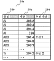
도 5는 물질 파장 대응표의 테이블 예를 나타내는 도면이다.
도 6은 OES 데이터의 테이블 예를 나타내는 도면이다.
도 7은 동일 물질간 상관 정보의 테이블 예를 나타내는 도면이다.
도 8은 주변 파장간 상관 정보의 테이블 예를 나타내는 도면이다.
도 9는 임계값 정보의 테이블 예를 나타내는 도면이다.
도 10은 추천 파장 정보의 테이블 예를 나타내는 도면이다.
도 11은 발광 강도 평균 정보의 테이블 예를 나타내는 도면이다.
도 12는 본 발명의 일 실시 형태에 따른 분석 장치의 처리 플로우를 도시하는 도면이다.
도 13은 파장간의 시계열 변화에 상관이 있는 경우의 예를 나타내는 도면이다.
도 14는 파장간의 시계열 변화에 상관이 없는 경우의 예를 나타내는 도면이다.
도 15는 본 발명의 일 실시 형태에 따른 표시 화면을 도시하는 도면이다.
도 16은 본 발명의 일 실시 형태에 따른 표시 화면을 도시하는 도면이다.1 is a configuration diagram showing a configuration of an etching apparatus according to an embodiment of the present invention.
2 is a configuration diagram showing a configuration of an etching section according to an embodiment of the present invention.
3 is a diagram for explaining an example of OES data.
4 is a diagram for explaining an example of a time series change of OES data at a specific wavelength.
Fig. 5 is a table showing an example of the material wavelength correspondence table. Fig.
6 is a diagram showing an example of a table of OES data.
7 is a table showing an example of correlation information between the same substances.
8 is a table showing an example of correlation information between adjacent wavelengths.
9 is a diagram showing an example of a table of threshold value information.
10 is a table showing an example of a table of recommended wavelength information.
11 is a table showing an example of a table of light emission intensity average information.
12 is a diagram showing the processing flow of the analyzer according to the embodiment of the present invention.
13 is a diagram showing an example of a case where there is a correlation with a time series change between wavelengths.
14 is a diagram showing an example of a case in which there is no correlation with a time series change between wavelengths.
15 is a diagram showing a display screen according to an embodiment of the present invention.
16 is a diagram showing a display screen according to an embodiment of the present invention.
이하, 본 발명의 실시 형태를 도면에 기초하여 설명한다. 또한, 실시 형태를 설명하기 위한 전체 도면에 있어서, 동일한 부재에는 원칙적으로 동일한 부호를 붙이고, 그 반복 설명은 생략한다.DESCRIPTION OF THE PREFERRED EMBODIMENTS Hereinafter, embodiments of the present invention will be described with reference to the drawings. In all the drawings for explaining the embodiments, the same members are denoted by the same reference numerals in principle and the repetitive description thereof will be omitted.
[에칭 장치][Etching Apparatus]
본 발명에서는 도 1의 에칭 장치의 구성도에 도시하는 바와 같이, 에칭 장치(1)는 에칭부(10)와 분석부(20)와 입력부(30)와 출력부(31)와 통신 IF부(32)를 갖고 이들은 버스(33)를 통해서 서로 접속되어 있다.1, the
에칭부(10)는 플라즈마 가공부(11)와 분광기(OES)(12)와 제어부(13)와 IF부(14)를 구비하고, 플라즈마 가공부(11)는 플라즈마를 발생시켜 웨이퍼를 가공하고, 분광기(OES)(12)는 에칭 처리가 행해지는 동안에 플라즈마의 발광 데이터인 OES 데이터를 취득한다. OES 데이터는 IF부(14)를 통해서 분석부(20)가 갖는 기억부(22)에 저장된다. 제어부(13)는 플라즈마 가공부(11)에서의 처리를 제어한다. 에칭부(10)의 상세를 후술하는 도 2에서 설명한다.The
분석부(20)는, 수집한 OES 데이터를 연산 처리하는 연산부(21)와, OES 데이터와 각 물질이 발하는 광의 파장을 나타내는 데이터와 연산 처리의 결과를 기억하는 기억부(22)와, IF부(210)를 구비하고, 연산부(21)는 OES 데이터보다 복수의 발광 강도의 시계열 데이터를 취득하고, 취득한 시계열 데이터간의 상관 계수 등의 유사도를 계산하고, 유사도의 크기로부터 에칭 처리의 모니터ㆍ감시ㆍ제어에 이용해야 할 파장을 특정하는 처리를 행한다. 연산부(21)가 행하는 연산 처리의 상세를 도 13에서 설명한다.The analyzing unit 20 includes an
입력부(30)는, 유저 조작에 의한 정보 입력을 접수하는 예를 들어 마우스나 키보드 등이다. 출력부(31)는, 유저에 대하여 정보를 출력하는 디스플레이나 프린터 등이다. 통신 IF부(32)는, 버스(33)나 외부 네트워크 등을 통해서 다른 장치나 시스템(기존의 생산 관리 시스템 등과도 접속 가능함)과 접속하고 정보 송수신을 행하기 위한 인터페이스이다. 버스(33)는, 각 부(10, 20, 30, 31, 32)를 연결한다. 각 부의 IF부(14, 29 등)는, 버스(33)를 통해서 정보 송수신을 행하기 위한 인터페이스이다. 또한, 분석부(20)가, 에칭 장치(1)의 외부에 분석 장치로서 접속되는 형태로 해도 좋다.The input unit 30 is, for example, a mouse or a keyboard that accepts information input by a user operation. The
[에칭부][Etching section]
에칭부(10)는 플라즈마 가공부(11)와 분광기(OES)(12)와 제어부(13)와 IF부(14)를 구비하고, 플라즈마 가공부(11)는 챔버(111)와 전극(112a, 112b)과 창(115)과 가스 공급기(117)를 구비하고 있다. 제어부(13)로부터의 지시에 의해 플라즈마 가공부(11)는 웨이퍼(114)를 챔버(111)의 내부에 저장하고, 가스 공급기(117)로부터 에칭 가스를 공급하고, 전극(112a, 112b)을 사용해서 전압을 거는 것에 의해 플라즈마화한 가스(113)를 웨이퍼(114)에 충돌시킴으로써 웨이퍼(114)를 가공한다. 가스(113)는, 가스 공급기(117)로부터 공급된 에칭 가스에 포함되는 물질이나 웨이퍼(114)로부터 가공의 과정에서 발생한 물질을 포함하고 있고, 가스에 포함되어 있는 물질에 따른 파장의 광(116)을 발생시킨다. 발생한 광은 창(115)을 통해서 분광기(OES)(12)에 의해 계측된다.The
[OES 데이터][OES data]
도 3에 분광기(OES)(12)에 의해 계측된 OES 데이터의 예를 나타낸다. OES 데이터는 파장과 시간의 이차원의 요소를 갖고, 각 파장, 각 시간에 대해서 각각 계측된 발광 강도의 값을 나타내고 있다. 도 4는 특정 파장에서의 발광 강도의 시계열 변화를 나타낸다. 도 4에 도시하는 바와 같이, 발광 강도의 값은 시간에 따라서 변화한다. 이 시계열 변화의 궤적은, 파장에 의해 다르다.FIG. 3 shows an example of OES data measured by the spectroscope (OES) 12. The OES data has two-dimensional elements of wavelength and time, and shows values of emission intensity measured for each wavelength and each time. Fig. 4 shows a time-series change in luminescence intensity at a specific wavelength. As shown in Fig. 4, the value of the light emission intensity varies with time. The locus of this time series change depends on the wavelength.
[분석부][Analysis department]
도 1에 도시하는 바와 같이, 분석부(20)는 연산부(21)와 기억부(22)와 IF부(210)를 구비하고, 기억부(22)는 물질 파장 대응표 기억 영역(23)과, OES 데이터 기억 영역(24)과, 동일 물질간 상관 정보 기억 영역(25)과, 주변 파장간 상관 정보 기억 영역(26)과, 임계값 정보 기억 영역(27)과, 추천 파장 정보 기억 영역(28)을 구비하고 있다.1, the analysis unit 20 includes an
물질 파장 대응표 기억 영역(23)에는, 가스(113)에 포함될 가능성이 있는 물질에 대해서, 그 물질이 발하는 광(116)의 파장을 특정하는 정보가 저장된다. 상기 물질은, 단일 원소 또는 복수 원소가 결합된 것이고, 각 물질이 발하는 광의 파장은 사전에 계측되어 특정된 것이다. 또한, 여기에 기재된 물질이 항상 가스(113)에 포함되는 것은 아니다. 또한, 각 물질이 발하는 광의 파장은, 에칭 장치(1)의 조건이 서로 달라도 동일 물질이면 동일하다.In the material wavelength correspondence
도 5는, 물질 파장 대응표 기억 영역(23)의 일 실시예인 물질 파장 대응표 테이블(23a)을 도시한다. 본 테이블은, 물질란(23b), 파장란(23c) 등의 각 필드를 갖는다.Fig. 5 shows a material wavelength correspondence table table 23a which is an embodiment of the material wavelength correspondence
물질란(23b)에는, 가스(113)에 포함될 가능성이 있는 물질을 특정하는 정보가 저장된다.In the
파장란(23c)에는, 물질란(23b)에서 특정된 물질이 발하는 광의 파장을 특정하는 정보가 저장된다. 파장란(23c)에서 특정되는 파장은, 1개 또는 복수의 물질에 대응지어진다.In the
또한, OES 데이터 중, 파장란(23c)에 저장된 파장에서의 발광 강도의 값은, 물질란(23b)에 대응지어진(동일 행에 저장된) 물질의 발광에 의해 결정된다고는 할 수 없다. 그 때문에, 파장란(23c)에 저장된 파장 중, 물질란(23b)에 대응지어진 물질의 발광에 의해 발광 강도의 값이 결정되는 것을 특정하는 것이, 플라즈마 가공부(11)의 모니터ㆍ감시ㆍ제어를 하는 데 있어서는 필요해진다.In addition, the value of the light emission intensity at the wavelength stored in the
OES 데이터 기억 영역(24)에는, 분광기(OES)(12)에 의해 계측된 OES 데이터를 특정하는 정보가 저장된다.In the OES
도 6은, OES 데이터 기억 영역(24)의 일 실시예인 OES 데이터 테이블(24a)을 도시한다. 본 테이블은, 파장란(24b), 시간란(24c), 발광 강도란(24d) 등의 각 필드를 갖는다.6 shows an OES data table 24a which is an embodiment of the OES
파장란(24b)에는, 계측된 OES 데이터의 파장을 특정하는 정보가 저장된다. 파장란(24b)에는, 전술한 물질 파장 대응표 테이블(23a)의 파장란(23c)에 저장된 값과 동일한 값이 저장된 열이 존재한다.In the
시간란(24c)에는, 계측된 OES 데이터의 시간을 특정하는 정보가 저장된다.In the
발광 강도란(24d)에는, 파장란(24b)에서 특정된 파장 및 시간란(24c)에서 특정된 시간에서의, OES 데이터의 발광 강도를 특정하는 정보가 저장된다.The light
동일 물질간 상관 정보 기억 영역(25)에는, OES 데이터 기억 영역(24)에 기억된 OES 데이터 중 물질 파장 대응표 기억 영역(23)에 기억된 파장에 해당하는 것에 대해서, 발광 강도의 시계열 데이터의 유사도인 상관 계수를 계산한 결과가 저장된다.In the same intermaterial correlation
도 7은, 동일 물질간 상관 정보 기억 영역(25)의 일 실시예인 동일 물질간 상관 정보 테이블(25a)을 도시한다. 본 테이블은, 물질란(25b), 파장란(열 방향)(25c), 파장란(행 방향)(25d), 발광 강도 상관 1란(25e) 등의 각 필드를 갖는다.7 shows the same-substance correlation information table 25a which is one embodiment of the same intermaterial correlation
물질란(25b)은, 파장란(열 방향)(25c) 및 파장란(행 방향)(25d)에 저장되는 값에 의해 특정되는 파장의 광을 발하는 물질의 명칭이 저장된다.The
파장란(열 방향)(25c)은, 물질란(25b)에 저장되는 값에 의해 특정되는 물질이, 물질 파장 대응표 테이블(23a)에 의해 대응지어져 있는 파장을 특정하는 정보가 저장된다.The wavelength column (column direction) 25c stores information specifying the wavelength associated with the material wavelength table table 23a by the substance specified by the value stored in the
파장란(행 방향)(25d)은, 파장란(열 방향)(25c)과 마찬가지로, 물질란(25b)에 저장되는 값에 의해 특정되는 물질이, 물질 파장 대응표 테이블(23a)에 의해 대응지어져 있는 파장을 특정하는 정보가 저장된다.As in the case of the wavelength column (column direction) 25c, the wavelength column (row direction) 25d has a wavelength corresponding to the material specified by the value stored in the
발광 강도 상관 1란(25e)은, 파장란(열 방향)(25c)에 저장되는 값에 의해 특정되는 파장에서의 발광 강도의 시계열 변화와, 파장란(행 방향)(25d)에 저장되는 값에 의해 특정되는 파장에서의 발광 강도의 시계열 변화와의, 유사도인 상관 계수를 특정하는 정보가 저장된다. 또한, 전술한 발광 강도의 시계열 변화는, OES 데이터 테이블(24a)에 의해 특정되는 값이다.The light
주변 파장간 상관 정보 기억 영역(26)에는, OES 데이터 기억 영역(24)에 기억된 OES 데이터 중 물질 파장 대응표 기억 영역(23)에 기억된 파장에 해당하는 것에 대해서, 발광 강도의 시계열 데이터의 유사도인 상관 계수를 계산한 결과가 저장된다.Wavelength correlation
도 8은, 주변 파장간 상관 정보 기억 영역(26)의 일 실시예인 주변 파장간 상관 정보 테이블(26a)을 도시한다. 본 테이블은, 물질란(26a), 파장란(26c), 주변 파장란(26d), 발광 강도 상관 2란(26e) 등의 각 필드를 갖는다.8 shows an inter-wavelength inter-correlation information table 26a, which is an embodiment of the inter-wavelength inter-correlation
물질란(26b)은, 물질 파장 대응표 테이블(23a)의 물질란(23b)에 저장되는 값에 대응하는 물질명이 저장된다.The
파장란(26c)은, 물질 파장 대응표 테이블(23a)의 파장란(23c)에 저장되는 값에 대응하는 파장의 값이 저장된다.The
주변 파장란(26d)은, 파장란(26c)에 저장되는 값에 의해 특정되는 파장을 기준으로 한, 파장의 주변 범위를 나타내는 정보가 저장된다. 도 8의 예에서는, 파장란(26c)에 저장되는 값으로부터 50을 뺀 값으로부터, 파장란(26c)에 저장되는 값으로부터 50을 더한 값까지가, 주변 파장란(26d)에 저장되어 있지만, 50 이외의 값이어도 좋고, 또한 뺀 값과 더한 값이 다른 값이 되어도 좋다.The
발광 강도 상관 2란(26e)은, 파장란(26c)에 저장되는 값에 의해 특정되는 파장에서의 발광 강도의 시계열 변화와, 주변 파장란(26d)에 저장되는 값에 의해 특정되는 파장의 범위에서 평균적인 발광 강도의 시계열 변화와의, 유사도인 상관 계수를 특정하는 정보가 저장된다. 또한, 전술한 발광 강도의 시계열 변화는, OES 데이터 테이블(24a)에 의해 특정되는 값이다. 전술한 평균적인 발광 강도의 시계열 변화는, 후술하는 발광 강도 평균 정보 테이블(29a)에 의해 특정되는 값이다.The light
임계값 정보 기억 영역(27)에는, 에칭부(10)의 모니터ㆍ감시ㆍ제어에 이용하는 데 적합한 파장을 선택하기 위한 조건이 저장된다.In the threshold value
도 9는, 임계값 정보 기억 영역(27)의 일 실시예인 임계값 정보 테이블(27a)을 도시한다. 본 테이블은, 임계값 1란(27b), 임계값 2란(27c), 임계값 3란(27d) 등의 각 필드를 갖는다.FIG. 9 shows a threshold value information table 27a which is an embodiment of the threshold value
임계값 1란(27b)은, 동일 물질간 상관 정보 테이블(25a)의 발광 강도 상관 1란(25e)에 있어서, 큰 상관 계수가 저장되어 있는 셀을 특정하기 위한 정보가 저장된다.The
임계값 2란(27c)은, 동일 물질간 상관 정보 테이블(25a)에 저장된 정보를 사용해서, 추천 파장으로 해야 할 파장을 특정하기 위한 정보가 저장된다.In the
임계값 3란(27d)은, 주변 파장간 상관 정보 테이블(26a)에 저장된 정보를 사용해서, 추천 파장으로 해야 할 파장을 특정하기 위한 정보가 저장된다.In the
추천 파장 정보 기억 영역(28)은 물질 파장 대응표 기억 영역(23)에 기억된 파장 중, 에칭부(10)의 모니터ㆍ감시ㆍ제어에 이용하는 파장을 특정하는 정보를 기억한다.The recommended wavelength
도 10은, 추천 파장 정보 기억 영역(28)의 일 실시예인 추천 파장 정보 테이블(28a)을 도시한다. 본 테이블은, 물질란(28a), 파장란(28c), 추천 파장란(28d) 등의 각 필드를 갖는다.Fig. 10 shows a recommended wavelength information table 28a which is an embodiment of the recommended wavelength
물질란(28b)은, 물질 파장 대응표 테이블(23a)의 물질란(23b)에 저장되는 값에 대응하는 물질명이 저장된다.The
파장란(28c)은, 물질 파장 대응표 테이블(23a)의 파장란(23c)에 저장되는 값에 대응하는 파장의 값이 저장된다.The
추천 파장란(28d)은, 파장란(28c)에 저장되는 값에 의해 특정되는 파장이, 에칭부(10)의 모니터ㆍ감시ㆍ제어에의 이용에 적합한 파장인 것을 특정하는 정보가 저장된다.In the recommended
발광 강도 평균 정보 기억 영역(29)은, OES 데이터 기억 영역(24)에 기억된 OES 데이터를 특정 파장 구간에서 평균적인 값을 특정하는 정보가 저장된다.The light emission intensity average
도 11은, 발광 강도 평균 정보 기억 영역(29)의 일 실시예인 발광 강도 평균 정보 테이블(29a)을 도시한다. 본 테이블은, 주변 파장란(29b), 시간란(29c), 발광 강도 평균란(29d) 등의 각 필드를 갖는다.11 shows the light emission intensity average information table 29a which is one embodiment of the light emission intensity average
주변 파장란(29b)은, 발광 강도 평균란(29d)에 저장되는 값에 의해 특정되는 발광 강도 평균을 산출한, 파장의 주변 범위를 특정하는 정보가 저장된다.The
시간란(29c)은, 발광 강도 평균란(29d)에 저장되는 값에 의해 특정되는 발광 강도 평균이 계측된 시간을 특정하는 정보가 저장된다.The
발광 강도 평균란(29d)에는, OES 데이터 테이블(24a)의 발광 강도란(24d)에 저장된 값을, 주변 파장란(29b)에 저장되는 값에 의해 특정되는 범위에서 평균화한 결과를 특정하는 정보가 저장된다.Information specifying the result of averaging the values stored in the light
[분석부(20)의 분석 처리][Analysis processing of the analysis unit 20]
도 12는, 분석부(20)의 주로 연산부(21)에 의한 분석 처리를 도시한다(S101등은 처리 스텝을 나타낸다). 도 12를 사용해서, 분석 처리를 설명한다.12 shows the analysis processing mainly performed by the
연산부(21)는 에칭부(10)에 의한 에칭 처리가 종료되거나, 혹은 유저에 의한 분석 처리의 실행 명령이 입력되면, 도 12에 도시하는 분석 처리를 실행한다. 분석 처리 실행의 단계에서, 물질 파장 대응표 테이블(23a), OES 데이터 테이블(24a), 임계값 정보 테이블(27a)에는 각각 값이 저장되어 있다. 물질 파장 대응표 테이블(23a)에는 과거의 실험에 의해 계측된 값이, OES 데이터 테이블(24a)에는 분광기(OES)(12)에 의해 계측된 값이, 임계값 정보 테이블(27a)에는 설계자에 의해 결정된 값이, 저장되어 있다.The
(S101)(S101)
S101에서는, 연산부(21)는, 각 데이터 테이블에 계산상 필요한 데이터를 저장한다.In S101, the
우선, 연산부(21)는 물질 파장 대응표 테이블(23a)의 물질란(23b)에 저장된 값을, 주변 파장간 상관 정보 테이블(26a)의 물질란(26b)에 저장하고, 물질 파장 대응표 테이블(23a)의 파장란(23c)에 저장된 값을, 파장란(26c)에, 저장한다.The
또한, 연산부(21)는 물질 파장 대응표 테이블(23a)의 물질란(23b)에 저장된 값을, 추천 파장 정보 테이블(28a)의 물질란(28b)에 저장하고, 물질 파장 대응표 테이블(23a)의 파장란(23c)에 저장된 값을, 파장란(28c)에, 저장한다.The
또한, 연산부(21)는 OES 데이터 테이블(24a)의 시간란(24c)에 저장된 값을, 발광 강도 평균 정보 테이블(29a)의 시간란(29c)에, 저장한다.The
S101 종료시에, 연산부는 물질 파장 대응표 테이블(23a)의 행 번호를 나타내는 값 i에 1을 저장한다.At the end of S101, the
(S102)(S102)
S102에서는, 연산부(21)는 OES 데이터 테이블(24a)의 정보를 입력으로서, 동일 물질간에서의 발광 강도의 시계열 데이터의 상관을 산출하고, 산출한 상관을 동일 물질 상관 정보 테이블(25a)에 저장한다.In step S102, the calculating
우선 연산부(21)는 동일 물질간 상관 정보 테이블(25a)의 전체 데이터를 소거한다.First, the
다음에, 물질 파장 대응표 테이블(23a)의 물질란(23b)의 i행째에 저장된 값(물질 i)을 읽어들이고, 동일 물질간 상관 정보 테이블(25a)의 물질란(25b)에 저장한다.Next, the value (substance i) stored in the i-th row of the
또한, 연산부(21)는 물질 파장 대응표 테이블(23a)의 물질란(23b)을 제1행째로부터 최종 행까지 주사하고, 물질 i와 동일한 값이 저장된 행에 대해서는, 파장란(23c)의 당해 행에 저장된 값을 파장란(열 방향)(25c)의 최종 열 및 파장란(행 방향)(25d)의 최하 행에 저장한다. 또한, 최종 열에 이미 값이 저장되어 있는 경우에는 최종 열에 1열 추가하고, 당해 열에 값을 저장한다. 또한, 최하 행에 이미 값이 저장되어 있는 경우도 마찬가지로, 최하 행에 1행 추가하고, 당해 행에 값을 저장한다. 이 처리에 의해, 동일 물질간 상관 정보 테이블(25a)의 파장란(열 방향)(25c) 및 파장란(행 방향)(25d)에는, 물질 i에 대응하는 파장을 특정하는 값이 저장되게 된다.The
또한, 연산부(21)는 발광 강도 상관 1란(25e)에 값을 저장한다. 파장란(열 방향)(25c)의 열 번호를 j로 하고, 파장란(행 방향)의 행 번호를 k로 두면, 발광 강도 상관 1란(25e)의 k행 j열에 저장되는 값(r1)은, 하기의 수학식 1에 의해 산출된다.Further, the calculating

수학식 1에서의 각 기호의 의미는 하기와 같다. The meanings of the symbols in the formula (1) are as follows.
p는, OES 데이터 테이블(24a)의 파장란(24b)에서, 파장란(열 방향)(25c)의 j열에 저장된 값과 동일한 값이 저장된 열의 번호를 나타낸다.p represents the number of the column in which the same value as the value stored in the jth column of the wavelength column (column direction) 25c in the
q는, OES 데이터 테이블(24a)의 파장란(24b)에서, 파장란(행 방향)(25d)의 k행에 저장된 값과 동일한 값이 저장된 열의 번호를 나타낸다.q indicates the number of the column in which the same value as the value stored in the row k of the wavelength column (row direction) 25d in the
xlp는, OES 데이터 테이블(24a)의 발광 강도란(24d)에 저장된 값 중, l행 p열에 저장된 값을 나타낸다.x lp represents the value stored in the lth row and pth column among the values stored in the light
xmp는, OES 데이터 테이블(24a)의 발광 강도란(24d)에 저장된 값 중, m행 p열에 저장된 값을 나타낸다.x mp represents a value stored in the mth row and the pth column among the values stored in the light
xlq는, OES 데이터 테이블(24a)의 발광 강도란(24d)에 저장된 값 중, l행 q열에 저장된 값을 나타낸다.x lq represents the value stored in the lth row and the qth column among the values stored in the light
xmq는, OES 데이터 테이블(24a)의 발광 강도란(24d)에 저장된 값 중, m행 q열에 저장된 값을 나타낸다.x mq represents a value stored in column m and row q of the values stored in the light
n은, OES 데이터 테이블(24a)의 발광 강도란(24d)의 행수를 나타내고 있다.n represents the number of rows of the light
r1은, 수학식 1에서 계산되는 값(상관 계수)이고, 발광 강도란(24d)의 p열에 저장된 값과, 발광 강도란(24d)의 q열에 저장된 값의, 시계열 변화의 유사도의 크기를 나타내고 있다.r 1 is a value (correlation coefficient) calculated in Equation (1), and the value of the value stored in the p column of the light emission intensity column (24d) and the value stored in the column q of the light emission intensity column (24d) Respectively.
도 13에, 발광 강도의 시계열 변화를 그래프화한 것과, 그 2개의 그래프로 나타내는 시계열 변화간의 상관 계수 r1의 값을 나타낸다. 2개의 그래프의 시계열 변화는 유사하고 있고, 상관 계수 r1도 큰 것을 알 수 있다.Fig. 13 shows values of the correlation coefficient r 1 between a time series change of the light emission intensity and a time series change represented by the two graphs. The time series changes of the two graphs are similar, and the correlation coefficient r 1 is also large.
또한, 수학식 1에서는, 상관 계수를 이용하고 있지만, 그 이외의 유사도를 평가하는 지표를 이용해도 좋다.Although the correlation coefficient is used in the equation (1), an index for evaluating other similarity may be used.
연산부(21)는 발광 강도 상관 1란(25e)의 행 및 열의 모든 조합에 대해서, 수학식 1을 사용해서 상관 계수를 산출하고, 산출한 값을 저장한다.The
(S103)(S103)
S103에서는, 연산부(21)는 OES 데이터 테이블(24a)의 정보를 입력으로서, i행째 파장의 주변의 파장에서의 발광 강도의 평균값을 산출하고, 발광 강도 평균 정보 테이블(29a)에 저장한다.In step S103, the
우선, 연산부(21)는 물질 파장 대응표 테이블(23a)의 파장란(23c)의 i행째에 저장된 값을 읽어들이고, 읽어들인 값을 기준으로 한 파장의 주변 범위를 결정한다. 본 실시예에서는, 읽어들인 값으로부터 50을 뺀 값을 범위의 최소값으로 하고, 읽어들인 값에 50을 더한 값을 범위의 최대값으로 한다.First, the
연산부(21)는, 결정한 범위를, 「범위의 최소값 내지 범위의 최대값」의 형식으로, 주변 파장간 상관 정보 테이블(26d)의 주변 파장란(26d)의 i행째와, 추천 파장 정보 데이터 테이블(29a)의 주변 파장란(29b)에 저장한다.The
다음에, 연산부(21)는 OES 데이터 테이블(24a)의 발광 강도란(24d)의 1행째로부터 최하 행에 대해서, 주변 파장에서의 발광 강도의 평균값을 하기의 수학식 2에 의해 산출하고, 산출한 값(Aveo)을 발광 강도 평균 정보 테이블(29a)의 발광 강도 평균란(29d)에 저장한다.Next, the

수학식 2에서의 각 기호의 의미는 하기와 같다.The meanings of the symbols in the formula (2) are as follows.
o는, OES 데이터 테이블(24a)의 발광 강도란(24d)에서의 행 번호를 나타낸다.o indicates the row number in the light
xos는, OES 데이터 테이블(24a)의 발광 강도란(24d)에 저장된 값 중, o행 s열에 저장된 값을 나타낸다.x os represents a value stored in the o row s column among the values stored in the light
λs는, OES 데이터 테이블(24a)의 파장란(24b)에 저장된 값 중, s열에 저장된 값을 나타낸다.? s represents the value stored in the s column among the values stored in the
λmin은, 전술한 범위의 최소값을 나타낸다.? min represents a minimum value of the above-mentioned range.
λmax는, 전술한 범위의 최대값을 나타낸다.? max represents the maximum value of the above-mentioned range.
λi는, 물질 파장 대응표 테이블(23a)의 파장란(23c)의 i행째에 저장된 값을 나타낸다.lambda i represents the value stored in the i-th line of the
u는, OES 데이터 테이블(24a)의 파장란(24c)의 열수를 나타낸다.and u represents the number of columns of the
Aveo는, 발광 강도 평균 정보 테이블(29a)의 발광 강도 평균란(29d)의 o행에 저장되는 값을 나타낸다.Ave o represents a value stored in the o row of the light emission intensity
수학식 2는, 주변 파장간 상관 정보 테이블(26d)의 주변 파장란(26d)의 i행째에 저장된 값의 범위에 포함되고, 또한, 물질 파장 대응표 테이블(23a)의 파장란(23c)의 i행째에 저장된 값에 일치하지 않고, 파장에 대해서 발광 강도의 평균을 산출하는 것을 의미하고 있다. 또한, 여기서는 i행째에 저장된 값과 일치하는 파장의 발광 강도를 평균값의 계산으로부터 제외하고 있지만, 포함시켜도 좋다.(2) is included in the range of the value stored in the i-th row of the
(S104)(S104)
S104에서는, 연산부(21)는 OES 데이터 테이블(24a)의 발광 강도란(24d)에 저장된 정보와, 발광 강도 평균 정보 테이블(29a)의 발광 강도 평균란(29d)에 저장된 정보로부터, 발광 강도의 시계열 데이터의 상관을 산출하고, 산출한 값을 주변 파장간 상관 정보 테이블(26a)의 발광 강도 상관 2란(26e)에 저장한다.In S104, the calculating
연산부(21)는 발광 강도 상관 2란(26e)의 i행째에, 하기의 수학식 3에 의해 산출되는 값(r2)을 저장한다.

수학식 3에서의 각 기호의 의미는 하기와 같다.The meanings of the symbols in the formula (3) are as follows.
p는, OES 데이터 테이블(24a)의 파장란(24b)에서, 파장란(23c)의 i행에 저장된 값과 동일한 값이 저장된 열의 번호를 나타낸다.p represents the number of the column in which the same value as the value stored in the i row of the
xlp는, OES 데이터 테이블(24a)의 발광 강도란(24d)에 저장된 값 중, l행 p열에 저장된 값을 나타낸다.x lp represents the value stored in the lth row and pth column among the values stored in the light
yl은, 발광 강도 평균 정보 테이블(29a)의 발광 강도란(29d)에 저장된 값 중, l행에 저장된 값을 나타낸다.y l represents a value stored in the first row among the values stored in the light
n은, OES 데이터 테이블(24a)의 발광 강도란(24d)의 행수를 나타내고 있다.n represents the number of rows of the light
r2는, 수학식 3에서 계산되는 값(상관 계수)이고, OES 데이터 테이블(24a)의 발광 강도란(24d)의 p열에 저장된 값과, 발광 강도란(24d)의 q열에 저장된 값의, 시계열 변화의 유사도의 크기를 나타내고 있다.r 2 is a value (correlation coefficient) calculated in
또한, 수학식 3에서는, 상관 계수를 이용하고 있지만, 그 이외의 유사도를 평가하는 지표를 이용해도 좋다.Although the correlation coefficient is used in the equation (3), an index for evaluating other similarity may be used.
(S105)(S105)
S105에서는, 연산부(21)는 동일 물질간 상관 정보 테이블(25a)에 저장된 정보를 사용해서, 물질 파장 대응표 테이블(23a)의 파장란(23c)의 i행째에 저장된 값에 의해 특정되는 파장이, 에칭부(10)의 모니터ㆍ감시ㆍ제어에 이용할 수 있는 파장인지 여부를 판정한다.In S105, using the information stored in the same intermaterial correlation information table 25a, the
연산부(21)는 동일 물질간 상관 정보 테이블(25a)의 발광 강도 상관 1란(25e)에 저장된 값을 입력으로서, 발광 강도 상관 1란(25e)에 저장된 값이, 임계값 정보 테이블(27a)의 임계값 1란(27b)에 저장된 값을 이상이 되는 비율(R1) 하기의 수학식 4를 사용해서 산출한다.The

수학식 4에서의 각 기호의 의미는 하기와 같다.The meanings of the symbols in the formula (4) are as follows.
v는, 동일 물질간 상관 정보 테이블(25a)의 파장란(행 방향)(25d)에 있어서, 파장란(23c)의 i행에 저장된 값과 동일한 값이 저장된 행의 번호를 나타낸다.v indicates the number of a row in which the same value as the value stored in the i row of the
w는, 동일 물질간 상관 정보 테이블(25a)의 발광 강도 상관 1란(25e)의 열 번호를 지정하는 값이다.w is a value designating the column number of the light
a는, 동일 물질간 상관 정보 테이블(25a)의 발광 강도 상관 1란(25e)의 열수를 나타낸다.a represents the number of columns of the light
zvw는, 동일 물질간 상관 정보 테이블(25a)의 발광 강도 상관 1란(25e)에 저장된 값 중, v행 w열에 저장된 값을 나타낸다.z vw represents the value stored in the v row w column among the values stored in the light
Th1은, 임계값 정보 테이블(27a)의 임계값 1란(27b)에 저장된 값이다.Th 1 is a value stored in the
λv는, 동일 물질간 상관 정보 테이블(25a)의 파장란(행 방향)(25d)에 저장된 값 중, v행에 저장된 값을 나타낸다.? v represents the value stored in the v row among the values stored in the wavelength column (row direction) 25d of the inter-substance correlation information table 25a.
λw는, 동일 물질간 상관 정보 테이블(25a)의 파장란(열 방향)(25c)에 저장된 값 중, w열에 저장된 값을 나타낸다.? w represents a value stored in the w column among the values stored in the wavelength column (column direction) 25c of the inter-substance correlation information table 25a.
R1은, 수학식 4에서 계산되는 값이고, 물질 파장 대응표 테이블(23a)의 파장란(23c)의 i행째에 저장된 값에 의해 특정되는 파장의 발광 강도의 상관 계수가, 임계값 1란(27b)에 의해 특정되는 값 이상인 것의 비율을 나타내고 있다. R1의 값이 큰 것은, 동일 물질에 대응지어진 파장의 발광 강도가, 유사한 시계열 변화를 하고 있는 것을 나타내고 있다. 유사한 시계열 변화를 하는 이유는, 그 대응지어진 물질의 양의 증감 등에 기인한다고 생각된다(물질의 양이 증가하면, 그 물질에 대응지은 파장의 발광 강도는 물질의 양의 증가량에 따라서 커진다). 그와 같은 파장의 발광 강도를 에칭부(10)의 모니터ㆍ감시ㆍ제어에 사용함으로써, 가스(113)에 포함되는 물질의 양 등을 파악할 수 있어, 에칭부(10)를 적절하게 모니터ㆍ감시ㆍ제어할 수 있다고 생각된다.R 1 is, the value is, the materials the wavelength correspondence table table (23a) pajangran (23c) i-th row correlation coefficient of the luminescence intensity of the wavelength that is specified by the value stored in the which is calculated in Equation (4), the
상기의 사고 방식 하에, 다음에 연산부(21)는 R1과 임계값 2란(27c)에 저장되는 값을 비교하고, R1이 임계값 2란(27c)에 저장되는 값 이상이면, 물질 파장 대응표 테이블(23a)의 파장란(23c)의 i행째에 저장된 값에 의해 특정되는 파장이, 에칭부(10)의 모니터ㆍ감시ㆍ제어에 이용할 수 있는 파장이라고 판정하고, S106의 처리로 진행한다. Under the above-mentioned thinking method, the calculating
R1이 임계값 2란(27c)에 저장되는 값보다도 작으면, 연산부(21)는 S107의 처리로 진행한다.If R 1 is smaller than the value stored in the
(S106)(S106)
S106에서는, 연산부(21)는 추천 파장 정보 테이블(28a)의 추천 파장란(28d)의 i행에, 에칭부(10)의 모니터ㆍ감시ㆍ제어에 이용할 수 있는 파장이라고 판정한 것을 나타내는 “추천 1”의 값을 저장한다.In step S106, the
(S107)(S107)
S107에서는, 연산부(21)는 동일 물질간 상관 정보 테이블(25a)에 저장된 정보를 사용해서, 물질 파장 대응표 테이블(23a)의 파장란(23c)의 i행째에 저장된 값에 의해 특정되는 파장이, 에칭부(10)의 모니터ㆍ감시ㆍ제어에 이용할 수 있는 파장인지 여부를 판정한다.In S107, the
연산부(21)는 주변 파장간 상관 정보 테이블(26a)의 발광 강도 상관 2란(26e)에 저장된 값과, 임계값 정보 테이블(27a)의 임계값 3란(27d)에 저장된 값을 비교하고, 발광 강도 상관 2란(26e)에 저장된 값이, 임계값 3란(27d)에 저장된 값보다도 작으면, 물질 파장 대응표 테이블(23a)의 파장란(23c)의 i행째에 저장된 값에 의해 특정되는 파장이, 에칭부(10)의 모니터ㆍ감시ㆍ제어에 이용할 수 있는 파장이라고 판정하고, S108의 처리로 진행한다.The calculating
주변 파장간 상관 정보 테이블(26a)의 발광 강도 상관 2란(26e)에 저장된 값이 작은 경우는, 도 14에 도시하는 바와 같이 물질 파장 대응표 테이블(23a)의 파장란(23c)의 i행째에 저장된 값에 의해 특정되는 파장의 발광 강도의 시계열 변화와, 주변의 파장에서의 발광 강도의 평균의 시계열 변화 사이의, 유사도가 작은 것을 나타내고 있다. 이 경우, 당해 파장의 발광 강도는, 그 대응지어진 물질의 양이나 온도 등에 기인하여 증감하는 것이라고 생각된다. 그와 같은 파장의 발광 강도를 에칭부(10)의 모니터ㆍ감시ㆍ제어에 사용함으로써, 가스(113)에 포함되는 물질의 양이나 온도 등을 파악할 수 있어, 에칭부(10)를 적절하게 모니터ㆍ감시ㆍ제어할 수 있다고 생각된다.If the value stored in the light
발광 강도 상관 2란(26e)에 저장된 값이, 임계값 3란(27d)에 저장된 값 이상이면, 연산부(21)는 S109의 처리로 진행한다.When the value stored in the light emission
(S108)(S108)
S108에서는, 연산부(21)는 추천 파장 정보 테이블(28a)의 추천 파장란(28d)의 i행에, 에칭부(10)의 모니터ㆍ감시ㆍ제어에 이용할 수 있는 파장이라고 판정한 것을 나타내는 “추천 2”의 값을 저장한다. 또한, 이미 “추천 1”의 값이 저장되어 있었던 경우는, “추천 1”과 “추천 2”를 병기한다.In step S108, the
(S109)(S109)
S109에서는, 연산부(21)는 S106 또는 S108의 처리를 실행한 경우에, 에칭부(10)의 모니터ㆍ감시ㆍ제어에 이용할 수 있는 파장을 유저에게 제시하는 처리를 행한다.In S109, the
추천 파장 정보 테이블(28a)의 추천 파장란(28d)의 i행에 “추천 1”의 값이 저장되어 있었던 경우는, 연산부(21)는 출력부(31)에 예를 들어 도 15에 도시하는 바와 같은 정보를 표시한다.When the value of
연산부(21)는, 챔버 내의 플라즈마에 포함되는 물질이 발하는 광을 나타내는 파장이라고 판정되고, 장치 제어 및 품질 해석에 사용하는 것을 추천이 되는 파장[물질 파장 대응표 테이블(23a)의 파장란(23c)의 i행째에 저장된 값]과 그 파장이 대응지어진 물질의 명칭[물질 파장 대응표 테이블(23a)의 물질란(23b)의 i행째에 저장된 값]을 표시한다.The
또한, 연산부(21)는, 추천으로 하는 파장의 발광 강도의 시계열 변화와, 추천으로 하는 파장과 동일 물질에 기인하는 파장의 발광 강도의 시계열 변화와의 상관 계수[동일 물질간 상관 정보 테이블(25a)의 발광 강도 상관 1란(25e)에 저장된 값]를 표시한다.The calculating
또한, 연산부(21)는, 추천으로 하는 파장의 발광 강도의 시계열 변화와, 추천으로 하는 파장과 동일 물질에 기인하는 파장의 발광 강도의 시계열 변화[OES 데이터 테이블(24a)의 발광 강도란(24d)에 저장된 값]를 그래프로서 표시한다.The
추천 파장 정보 테이블(28a)의 추천 파장란(28d)의 i행에 “추천 2”의 값이 저장되어 있었던 경우는, 연산부(21)는 출력부(31)에 예를 들어 도 16에 도시하는 바와 같은 정보를 표시한다.In the case where a value of "
연산부(21)는, 추천으로 하는 파장[물질 파장 대응표 테이블(23a)의 파장란(23c)의 i행째에 저장된 값]과 그 파장이 대응지어진 물질의 명칭[물질 파장 대응표 테이블(23a)의 물질란(23b)의 i행째에 저장된 값]을 표시한다.The
또한, 연산부(21)는, 추천으로 하는 파장의 발광 강도의 시계열 변화와, 추천으로 하는 파장의 주변 파장에서의 발광 강도 평균의 시계열 변화와의 상관 계수[주변 파장간 상관 정보 테이블(26a)의 발광 강도 상관 2란(26e)에 저장된 값]를 표시한다.The calculating
또한, 연산부(21)는, 추천으로 하는 파장의 발광 강도의 시계열 변화[OES 데이터 테이블(24a)의 발광 강도란(24d)에 저장된 값]와, 추천으로 하는 파장과 동일 물질에 기인하는 파장의 발광 강도의 시계열 변화[발광 강도 평균 정보 테이블(29a)의 발광 강도 평균란(29d)에 저장된 값]를 그래프로서 표시한다.The
(S110)(S110)
S110에서는, 연산부(21)는, 물질 파장 대응표 테이블(23a)의 파장란(23c)의 최하 행에 도달하고 있는 경우는 처리를 종료하고, 최하 행에 도달하지 않은 경우는, i에 1을 더하여, 물질 파장 대응표 테이블(23a)의 파장란(23c)의 다음 행에 대해서 계산을 실행한다.In S110, the
이상 설명한 바와 같이, 본 실시 형태의 에칭 장치(1)[분석부(20)]에서는, 분광기(OES)가 계측한 데이터와, 각각의 물질이 발하는 광의 파장의 정보 등을 입력 정보로서, 가스(113)의 특성[가스(113)에 포함되는 물질의 양이나 온도 등]을 적절하게 파악할 수 있는 파장을 제시할 수 있다. 에칭 장치(1)의 제어부(13)는 제시된 파장의 발광 강도를 입력으로서, 챔버(111)에 공급하는 가스의 양이나 온도, 전압 등을 적절하게 제어함으로써, 에칭 처리를 보다 효율적으로 행할 수 있다.As described above, in the etching apparatus 1 (analysis unit 20) of the present embodiment, data measured by the spectroscope (OES), information on the wavelength of light emitted by each material, 113] (the amount of the substance contained in the
또한, 다수의 후보를 갖는 OES 데이터의 파장 중으로부터, 모니터ㆍ감시ㆍ제어에 이용하는 파장을 자동적으로 선정할 수 있으므로, 큰 공수가 가해지는 에칭 데이터의 해석을 삭감하여, 효율적으로 에칭의 모니터ㆍ감시ㆍ제어를 하는 것이 가능해진다.Further, since the wavelength used for monitoring, monitoring, and control can be automatically selected from among the wavelengths of the OES data having a large number of candidates, the analysis of etching data to which a large number of holes are applied can be reduced, It becomes possible to perform control.
이상, 본 발명을 실시 형태에 기초하여 구체적으로 설명하였지만, 본 발명은 상기 실시 형태에 한정되는 것이 아니라, 그 요지를 일탈하지 않는 범위에서 다양하게 변경 가능하다.While the present invention has been described in detail with reference to the embodiment thereof, it is to be understood that the present invention is not limited to the above-described embodiments but may be variously changed without departing from the gist of the invention.
1 : 에칭 장치
10 : 에칭부
11 : 플라즈마 가공부
12 : 분광기(OES)
13 : 제어부
14 : IF부
20 : 분석부
21 : 연산부
22 : 기억부
23 : 물질 파장 대응표 기억 영역
24 : OES 데이터 기억 영역
25 : 동일 물질간 상관 정보 기억 영역
26 : 주변 파장간 상관 정보 기억 영역
27 : 임계값 정보 기억 영역
28 : 추천 파장 정보 기억 영역
29 : 발광 강도 평균 정보 기억 영역
210 : IF부
30 : 입력부
31 : 출력부
32 : 통신 IF부
33 : 버스1: etching apparatus
10:
11: Plasma processing section
12: spectroscope (OES)
13:
14: IF section
20: Analytical Department
21:
22:
23: Material wavelength correspondence table storage area
24: OES data storage area
25: inter-substance correlation information storage area
26: Correlation information storage area between surrounding wavelengths
27: Threshold value information storage area
28: Recommended wavelength information storage area
29: Light emission intensity average information storage area
210: IF section
30: Input unit
31: Output section
32: Communication IF section
33: Bus
Claims (15)
미리 특정된 물질이 발광하는 복수의 파장의 파장마다 상기 계측된 발광의 발광 강도가 시간에 따라서 변화하는 제1 시계열 변화를 구하는 스텝과,
미리 특정된 물질이 발광하는 파장으로부터 소정의 거리에 있는 주변 파장의 파장마다 상기 계측된 발광의 발광 강도가 시간에 따라서 변화하는 제2 시계열 변화를 구하는 스텝과,
상기 제1 시계열 변화의 파장 간의 상관을 나타내는 제1 상관 값을 상기 미리 특정된 물질마다 산출하는 스텝과,
상기 제1 시계열 변화와 상기 제2 시계열 변화 사이의 상관을 나타내는 제2 상관 값을 파장마다 산출하는 스텝과,
상기 제1 상관 값 또는 상기 제2 상관 값을 사용하여 상기 챔버 내의 플라즈마에 포함되는 물질이 발하는 광의 파장을 특정하는 스텝
을 갖는 것을 특징으로 하는 분석 방법.Measuring light emission in a chamber during an etching process of a semiconductor wafer,
Obtaining a first time-series change in which the light emission intensity of the measured light emission varies with time for each of a plurality of wavelengths at which a predetermined substance is emitted,
Obtaining a second time-series change in which the light emission intensity of the measured light emission varies with time for each wavelength of an ambient wavelength at a predetermined distance from a wavelength at which a specified substance is emitted,
Calculating a first correlation value indicating a correlation between wavelengths of the first time series change for each of the predetermined substances,
Calculating, for each wavelength, a second correlation value indicating a correlation between the first time series change and the second time series change;
Using the first correlation value or the second correlation value to identify the wavelength of light emitted by the material contained in the plasma in the chamber
Lt; / RTI >
상기 주변 파장에서의 발광 강도의 시계열 변화는, 상기 미리 특정된 물질이 발광하는 파장으로부터 소정의 거리에 있는 파장까지의 발광 강도의 평균값의 시계열 변화인 것을 특징으로 하는 분석 방법.The method according to claim 1,
Wherein the time series change of the light emission intensity at the peripheral wavelength is a time series change of an average value of the light emission intensities from a wavelength at which the predetermined substance is emitted to a wavelength at a predetermined distance.
미리 특정된 물질이 발광하는 복수의 파장의 파장마다 상기 수신한 발광의 발광 강도가 시간에 따라서 변화하는 제1 시계열 변화를 구하는 수단과,
미리 특정된 물질이 발광하는 파장으로부터 소정의 거리에 있는 주변 파장의 파장마다 수신한 발광의 발광 강도가 시간에 따라서 변화하는 제2 시계열 변화를 구하는 수단과,
상기 제1 시계열 변화의 파장 간의 상관을 나타내는 제1 상관 값을 상기 미리 특정된 물질마다 산출하는 수단과,
상기 제1 시계열 변화와 상기 제2 시계열 변화 사이의 상관을 나타내는 제2 상관 값을 파장마다 산출하는 수단과,
상기 제1 상관 값 또는 상기 제2 상관 값을 사용하여 상기 챔버 내의 플라즈마에 포함되는 물질이 발하는 광의 파장을 특정하는 수단
을 갖는 것을 특징으로 하는 분석 장치.Means for receiving an emission value in a chamber measured during an etching process of a semiconductor wafer,
Means for obtaining a first time-series change in which the light emission intensity of the received light emission changes with time for each of a plurality of wavelengths of light emitted by a predetermined substance,
Means for obtaining a second time-series change in which the light emission intensity of the light emission received for each wavelength of the peripheral wavelength at a predetermined distance from the wavelength at which the specified substance is emitted changes with time;
Means for calculating a first correlation value indicating a correlation between wavelengths of the first time series change for each of the predetermined substances;
Means for calculating, for each wavelength, a second correlation value indicating a correlation between the first time series change and the second time series change;
Means for determining the wavelength of the light emitted by the material contained in the plasma in the chamber using the first correlation value or the second correlation value
And an analyzer.
상기 주변 파장에서의 발광 강도의 시계열 변화는, 상기 미리 특정된 물질이 발광하는 파장으로부터 소정의 거리에 있는 파장까지의 발광 강도의 평균값의 시계열 변화인 것을 특징으로 하는 분석 장치.The method of claim 3,
Wherein the time series change of the light emission intensity at the peripheral wavelength is a time series change of an average value of the light emission intensities from a wavelength at which the predetermined substance is emitted to a wavelength at a predetermined distance.
상기 분석 장치는, 상기 반도체 웨이퍼의 에칭 처리 중에 계측된 챔버 내의 발광 값을 수신하는 수단과,
미리 특정된 물질이 발광하는 복수의 파장의 파장마다 상기 수신한 발광의 발광 강도가 시간에 따라서 변화하는 제1 시계열 변화를 구하는 수단과,
미리 특정된 물질이 발광하는 파장으로부터 소정의 거리에 있는 주변 파장의 파장마다 수신한 발광의 발광 강도가 시간에 따라서 변화하는 제2 시계열 변화를 구하는 수단과,
상기 제1 시계열 변화의 파장 간의 상관을 나타내는 제1 상관 값을 상기 미리 특정된 물질마다 산출하는 수단과,
상기 제1 시계열 변화와 상기 제2 시계열 변화 사이의 상관을 나타내는 제2 상관 값을 파장마다 산출하는 수단과,
상기 제1 상관 값 또는 상기 제2 상관 값을 사용하여 상기 챔버 내의 플라즈마에 포함되는 물질이 발하는 광의 파장을 특정하는 수단
을 구비하는 것을 특징으로 하는 에칭 처리 시스템.An etching apparatus for etching the semiconductor wafer in the chamber and a means for measuring the intensity of light emission in the chamber and an etching apparatus for etching the semiconductor wafer and an analyzing apparatus for analyzing the state of the etching process As a system,
The analyzing apparatus includes means for receiving a light emission value in a chamber measured during the etching process of the semiconductor wafer,
Means for obtaining a first time-series change in which the light emission intensity of the received light emission changes with time for each of a plurality of wavelengths of light emitted by a predetermined substance,
Means for obtaining a second time-series change in which the light emission intensity of the light emission received for each wavelength of the peripheral wavelength at a predetermined distance from the wavelength at which the specified substance is emitted changes with time;
Means for calculating a first correlation value indicating a correlation between wavelengths of the first time series change for each of the predetermined substances;
Means for calculating, for each wavelength, a second correlation value indicating a correlation between the first time series change and the second time series change;
Means for determining the wavelength of the light emitted by the material contained in the plasma in the chamber using the first correlation value or the second correlation value
And an etching system for etching the substrate.
상기 주변 파장에서의 발광 강도의 시계열 변화는, 상기 미리 특정된 물질이 발광하는 파장으로부터 소정의 거리에 있는 파장까지의 발광 강도의 평균값의 시계열 변화인 것을 특징으로 하는 에칭 처리 시스템.6. The method of claim 5,
Wherein the time series change of the light emission intensity at the peripheral wavelength is a time series change of an average value of the light emission intensities from a wavelength at which the predetermined substance is emitted to a wavelength at a predetermined distance.
Applications Claiming Priority (2)
| Application Number | Priority Date | Filing Date | Title |
|---|---|---|---|
| JPJP-P-2012-161130 | 2012-07-20 | ||
| JP2012161130A JP6002487B2 (en) | 2012-07-20 | 2012-07-20 | Analysis method, analysis apparatus, and etching processing system |
Publications (2)
| Publication Number | Publication Date |
|---|---|
| KR20140011996A KR20140011996A (en) | 2014-01-29 |
| KR101571928B1 true KR101571928B1 (en) | 2015-11-25 |
Family
ID=49946298
Family Applications (1)
| Application Number | Title | Priority Date | Filing Date |
|---|---|---|---|
| KR1020130085658A KR101571928B1 (en) | 2012-07-20 | 2013-07-19 | Analysis method, analysis apparatus and etching process system |
Country Status (4)
| Country | Link |
|---|---|
| US (1) | US9091595B2 (en) |
| JP (1) | JP6002487B2 (en) |
| KR (1) | KR101571928B1 (en) |
| TW (1) | TWI517246B (en) |
Cited By (2)
| Publication number | Priority date | Publication date | Assignee | Title |
|---|---|---|---|---|
| US10770273B2 (en) | 2018-02-09 | 2020-09-08 | Samsung Electronics Co., Ltd. | OES device, plasma processing apparatus including the same and method of fabricating semiconductor device |
| US10825666B2 (en) | 2018-08-27 | 2020-11-03 | Samsung Electronics Co., Ltd. | Plasma monitoring apparatus and plasma processing system |
Families Citing this family (13)
| Publication number | Priority date | Publication date | Assignee | Title |
|---|---|---|---|---|
| JP6239294B2 (en) | 2013-07-18 | 2017-11-29 | 株式会社日立ハイテクノロジーズ | Plasma processing apparatus and method of operating plasma processing apparatus |
| US9293303B2 (en) * | 2013-08-30 | 2016-03-22 | Taiwan Semiconductor Manufacturing Company, Ltd. | Low contamination chamber for surface activation |
| JP6173851B2 (en) * | 2013-09-20 | 2017-08-02 | 株式会社日立ハイテクノロジーズ | Analysis method and plasma etching apparatus |
| JP6220319B2 (en) * | 2014-07-17 | 2017-10-25 | 株式会社日立ハイテクノロジーズ | Data analysis method, plasma etching method, and plasma processing apparatus |
| WO2016105036A1 (en) * | 2014-12-22 | 2016-06-30 | 주식회사 두산 | Organic electroluminescent element |
| KR20160120382A (en) | 2015-04-07 | 2016-10-18 | 삼성전자주식회사 | Apparatus for optical emission spectroscopy and apparatus for treating plasma |
| JP6549917B2 (en) * | 2015-06-26 | 2019-07-24 | 株式会社日立ハイテクノロジーズ | Plasma processing apparatus and data analysis apparatus therefor |
| KR102415329B1 (en) | 2015-09-08 | 2022-06-30 | 삼성전자주식회사 | Tube-type lens, OES(Optical Emission Spectroscopy) apparatus comprising the tube-type lens, plasma monitoring system comprising the OES apparatus, and method for fabricating semiconductor device using the system |
| US10215704B2 (en) * | 2017-03-02 | 2019-02-26 | Tokyo Electron Limited | Computed tomography using intersecting views of plasma using optical emission spectroscopy during plasma processing |
| WO2021130798A1 (en) * | 2019-12-23 | 2021-07-01 | 株式会社日立ハイテク | Plasma treatment method and wavelength selecting method used for plasma treatment |
| JP7467292B2 (en) | 2020-03-13 | 2024-04-15 | 東京エレクトロン株式会社 | Analysis device, analysis method, and analysis program |
| JP7253668B2 (en) * | 2021-03-15 | 2023-04-06 | 株式会社日立ハイテク | Plasma processing apparatus and plasma processing method |
| KR20230012457A (en) * | 2021-07-14 | 2023-01-26 | 주식회사 히타치하이테크 | Plasma processing device, data analysis device, and semiconductor device manufacturing system |
Citations (2)
| Publication number | Priority date | Publication date | Assignee | Title |
|---|---|---|---|---|
| JP2003092286A (en) | 2001-09-18 | 2003-03-28 | Sumitomo Precision Prod Co Ltd | Method and device for detecting plasma etching end point |
| US20090211706A1 (en) * | 2008-02-27 | 2009-08-27 | Hitachi High-Technologies Corporation | Etching endpoint determination method |
Family Cites Families (11)
| Publication number | Priority date | Publication date | Assignee | Title |
|---|---|---|---|---|
| JPH05206074A (en) * | 1992-01-28 | 1993-08-13 | Kokusai Electric Co Ltd | Plasma etching end point detecting method and device |
| JPH09306894A (en) | 1996-05-17 | 1997-11-28 | Sony Corp | Optimum emission spectrum automatic detecting system |
| US6153115A (en) * | 1997-10-23 | 2000-11-28 | Massachusetts Institute Of Technology | Monitor of plasma processes with multivariate statistical analysis of plasma emission spectra |
| TW512248B (en) * | 1998-07-15 | 2002-12-01 | Toshiba Corp | Manufacturing method and apparatus of semiconductor device |
| JP4051470B2 (en) * | 1999-05-18 | 2008-02-27 | 東京エレクトロン株式会社 | End point detection method |
| WO2004102642A2 (en) * | 2003-05-09 | 2004-11-25 | Unaxis Usa Inc. | Envelope follower end point detection in time division multiplexed processes |
| JP4086190B2 (en) | 2003-09-02 | 2008-05-14 | 株式会社日立ハイテクノロジーズ | Emission spectrum causative substance identification support apparatus and support method |
| JP2008218898A (en) * | 2007-03-07 | 2008-09-18 | Hitachi High-Technologies Corp | Plasma processing device |
| JP5383265B2 (en) * | 2009-03-17 | 2014-01-08 | 株式会社日立ハイテクノロジーズ | Etching apparatus, analysis apparatus, etching processing method, and etching processing program |
| JP5778893B2 (en) * | 2010-03-19 | 2015-09-16 | 株式会社東芝 | End point detection apparatus, plasma processing apparatus, and end point detection method |
| JP5648157B2 (en) | 2011-12-28 | 2015-01-07 | 株式会社日立ハイテクノロジーズ | Semiconductor manufacturing equipment |
-
2012
- 2012-07-20 JP JP2012161130A patent/JP6002487B2/en active Active
-
2013
- 2013-07-18 US US13/945,285 patent/US9091595B2/en active Active
- 2013-07-18 TW TW102125810A patent/TWI517246B/en active
- 2013-07-19 KR KR1020130085658A patent/KR101571928B1/en active IP Right Grant
Patent Citations (3)
| Publication number | Priority date | Publication date | Assignee | Title |
|---|---|---|---|---|
| JP2003092286A (en) | 2001-09-18 | 2003-03-28 | Sumitomo Precision Prod Co Ltd | Method and device for detecting plasma etching end point |
| US20090211706A1 (en) * | 2008-02-27 | 2009-08-27 | Hitachi High-Technologies Corporation | Etching endpoint determination method |
| JP2009206275A (en) | 2008-02-27 | 2009-09-10 | Hitachi High-Technologies Corp | Etching end point determining method |
Cited By (2)
| Publication number | Priority date | Publication date | Assignee | Title |
|---|---|---|---|---|
| US10770273B2 (en) | 2018-02-09 | 2020-09-08 | Samsung Electronics Co., Ltd. | OES device, plasma processing apparatus including the same and method of fabricating semiconductor device |
| US10825666B2 (en) | 2018-08-27 | 2020-11-03 | Samsung Electronics Co., Ltd. | Plasma monitoring apparatus and plasma processing system |
Also Published As
| Publication number | Publication date |
|---|---|
| US9091595B2 (en) | 2015-07-28 |
| TWI517246B (en) | 2016-01-11 |
| JP6002487B2 (en) | 2016-10-05 |
| TW201409565A (en) | 2014-03-01 |
| KR20140011996A (en) | 2014-01-29 |
| JP2014022621A (en) | 2014-02-03 |
| US20140022540A1 (en) | 2014-01-23 |
Similar Documents
| Publication | Publication Date | Title |
|---|---|---|
| KR101571928B1 (en) | Analysis method, analysis apparatus and etching process system | |
| KR101215367B1 (en) | Etching apparatus, analysis apparatus, etching treatment method, and computer readable medium recording etching treatment program | |
| US9443704B2 (en) | Data analysis method for plasma processing apparatus, plasma processing method and plasma processing apparatus | |
| US20020104832A1 (en) | Plasma processing apparatus and method | |
| TWI546638B (en) | Plasma processing device, plasma processing method and analysis method | |
| KR102045241B1 (en) | Plasma processing apparatus and plasma processing system | |
| US20220328286A1 (en) | Analysis method and semiconductor etching apparatus | |
| JP6549917B2 (en) | Plasma processing apparatus and data analysis apparatus therefor | |
| KR101495621B1 (en) | Plasma apparatus and analyzing apparatus | |
| US11404253B2 (en) | Plasma processing apparatus and analysis method for analyzing plasma processing data | |
| KR102100210B1 (en) | Plasma processing apparatus | |
| KR20230012457A (en) | Plasma processing device, data analysis device, and semiconductor device manufacturing system |
Legal Events
| Date | Code | Title | Description |
|---|---|---|---|
| A201 | Request for examination | ||
| E902 | Notification of reason for refusal | ||
| E902 | Notification of reason for refusal | ||
| E701 | Decision to grant or registration of patent right | ||
| GRNT | Written decision to grant | ||
| FPAY | Annual fee payment |
Payment date: 20181101 Year of fee payment: 4 |