KR101545279B1 - vel Diblock Copolymer, Preparation Method Thereof, And Method Of Forming Nano Pattern Using The Same - Google Patents
vel Diblock Copolymer, Preparation Method Thereof, And Method Of Forming Nano Pattern Using The Same Download PDFInfo
- Publication number
- KR101545279B1 KR101545279B1 KR1020120027392A KR20120027392A KR101545279B1 KR 101545279 B1 KR101545279 B1 KR 101545279B1 KR 1020120027392 A KR1020120027392 A KR 1020120027392A KR 20120027392 A KR20120027392 A KR 20120027392A KR 101545279 B1 KR101545279 B1 KR 101545279B1
- Authority
- KR
- South Korea
- Prior art keywords
- thin film
- formula
- diblock copolymer
- solvent
- soft segment
- Prior art date
Links
Images


Classifications
-
- B—PERFORMING OPERATIONS; TRANSPORTING
- B82—NANOTECHNOLOGY
- B82Y—SPECIFIC USES OR APPLICATIONS OF NANOSTRUCTURES; MEASUREMENT OR ANALYSIS OF NANOSTRUCTURES; MANUFACTURE OR TREATMENT OF NANOSTRUCTURES
- B82Y10/00—Nanotechnology for information processing, storage or transmission, e.g. quantum computing or single electron logic
-
- G—PHYSICS
- G03—PHOTOGRAPHY; CINEMATOGRAPHY; ANALOGOUS TECHNIQUES USING WAVES OTHER THAN OPTICAL WAVES; ELECTROGRAPHY; HOLOGRAPHY
- G03F—PHOTOMECHANICAL PRODUCTION OF TEXTURED OR PATTERNED SURFACES, e.g. FOR PRINTING, FOR PROCESSING OF SEMICONDUCTOR DEVICES; MATERIALS THEREFOR; ORIGINALS THEREFOR; APPARATUS SPECIALLY ADAPTED THEREFOR
- G03F7/00—Photomechanical, e.g. photolithographic, production of textured or patterned surfaces, e.g. printing surfaces; Materials therefor, e.g. comprising photoresists; Apparatus specially adapted therefor
- G03F7/0002—Lithographic processes using patterning methods other than those involving the exposure to radiation, e.g. by stamping
-
- B—PERFORMING OPERATIONS; TRANSPORTING
- B82—NANOTECHNOLOGY
- B82Y—SPECIFIC USES OR APPLICATIONS OF NANOSTRUCTURES; MEASUREMENT OR ANALYSIS OF NANOSTRUCTURES; MANUFACTURE OR TREATMENT OF NANOSTRUCTURES
- B82Y40/00—Manufacture or treatment of nanostructures
-
- C—CHEMISTRY; METALLURGY
- C08—ORGANIC MACROMOLECULAR COMPOUNDS; THEIR PREPARATION OR CHEMICAL WORKING-UP; COMPOSITIONS BASED THEREON
- C08F—MACROMOLECULAR COMPOUNDS OBTAINED BY REACTIONS ONLY INVOLVING CARBON-TO-CARBON UNSATURATED BONDS
- C08F22/00—Homopolymers and copolymers of compounds having one or more unsaturated aliphatic radicals each having only one carbon-to-carbon double bond, and at least one being terminated by a carboxyl radical and containing at least one other carboxyl radical in the molecule; Salts, anhydrides, esters, amides, imides or nitriles thereof
- C08F22/36—Amides or imides
- C08F22/38—Amides
-
- C—CHEMISTRY; METALLURGY
- C08—ORGANIC MACROMOLECULAR COMPOUNDS; THEIR PREPARATION OR CHEMICAL WORKING-UP; COMPOSITIONS BASED THEREON
- C08F—MACROMOLECULAR COMPOUNDS OBTAINED BY REACTIONS ONLY INVOLVING CARBON-TO-CARBON UNSATURATED BONDS
- C08F293/00—Macromolecular compounds obtained by polymerisation on to a macromolecule having groups capable of inducing the formation of new polymer chains bound exclusively at one or both ends of the starting macromolecule
- C08F293/005—Macromolecular compounds obtained by polymerisation on to a macromolecule having groups capable of inducing the formation of new polymer chains bound exclusively at one or both ends of the starting macromolecule using free radical "living" or "controlled" polymerisation, e.g. using a complexing agent
-
- H—ELECTRICITY
- H01—ELECTRIC ELEMENTS
- H01L—SEMICONDUCTOR DEVICES NOT COVERED BY CLASS H10
- H01L21/00—Processes or apparatus adapted for the manufacture or treatment of semiconductor or solid state devices or of parts thereof
- H01L21/02—Manufacture or treatment of semiconductor devices or of parts thereof
- H01L21/04—Manufacture or treatment of semiconductor devices or of parts thereof the devices having at least one potential-jump barrier or surface barrier, e.g. PN junction, depletion layer or carrier concentration layer
- H01L21/18—Manufacture or treatment of semiconductor devices or of parts thereof the devices having at least one potential-jump barrier or surface barrier, e.g. PN junction, depletion layer or carrier concentration layer the devices having semiconductor bodies comprising elements of Group IV of the Periodic System or AIIIBV compounds with or without impurities, e.g. doping materials
- H01L21/30—Treatment of semiconductor bodies using processes or apparatus not provided for in groups H01L21/20 - H01L21/26
- H01L21/302—Treatment of semiconductor bodies using processes or apparatus not provided for in groups H01L21/20 - H01L21/26 to change their surface-physical characteristics or shape, e.g. etching, polishing, cutting
- H01L21/306—Chemical or electrical treatment, e.g. electrolytic etching
- H01L21/3065—Plasma etching; Reactive-ion etching
-
- B—PERFORMING OPERATIONS; TRANSPORTING
- B81—MICROSTRUCTURAL TECHNOLOGY
- B81C—PROCESSES OR APPARATUS SPECIALLY ADAPTED FOR THE MANUFACTURE OR TREATMENT OF MICROSTRUCTURAL DEVICES OR SYSTEMS
- B81C1/00—Manufacture or treatment of devices or systems in or on a substrate
- B81C1/00388—Etch mask forming
- B81C1/00396—Mask characterised by its composition, e.g. multilayer masks
-
- B—PERFORMING OPERATIONS; TRANSPORTING
- B81—MICROSTRUCTURAL TECHNOLOGY
- B81C—PROCESSES OR APPARATUS SPECIALLY ADAPTED FOR THE MANUFACTURE OR TREATMENT OF MICROSTRUCTURAL DEVICES OR SYSTEMS
- B81C2201/00—Manufacture or treatment of microstructural devices or systems
- B81C2201/01—Manufacture or treatment of microstructural devices or systems in or on a substrate
- B81C2201/0101—Shaping material; Structuring the bulk substrate or layers on the substrate; Film patterning
- B81C2201/0147—Film patterning
- B81C2201/0149—Forming nanoscale microstructures using auto-arranging or self-assembling material
-
- B—PERFORMING OPERATIONS; TRANSPORTING
- B81—MICROSTRUCTURAL TECHNOLOGY
- B81C—PROCESSES OR APPARATUS SPECIALLY ADAPTED FOR THE MANUFACTURE OR TREATMENT OF MICROSTRUCTURAL DEVICES OR SYSTEMS
- B81C2201/00—Manufacture or treatment of microstructural devices or systems
- B81C2201/01—Manufacture or treatment of microstructural devices or systems in or on a substrate
- B81C2201/0198—Manufacture or treatment of microstructural devices or systems in or on a substrate for making a masking layer
-
- C—CHEMISTRY; METALLURGY
- C08—ORGANIC MACROMOLECULAR COMPOUNDS; THEIR PREPARATION OR CHEMICAL WORKING-UP; COMPOSITIONS BASED THEREON
- C08F—MACROMOLECULAR COMPOUNDS OBTAINED BY REACTIONS ONLY INVOLVING CARBON-TO-CARBON UNSATURATED BONDS
- C08F220/00—Copolymers of compounds having one or more unsaturated aliphatic radicals, each having only one carbon-to-carbon double bond, and only one being terminated by only one carboxyl radical or a salt, anhydride ester, amide, imide or nitrile thereof
- C08F220/02—Monocarboxylic acids having less than ten carbon atoms; Derivatives thereof
- C08F220/52—Amides or imides
- C08F220/54—Amides, e.g. N,N-dimethylacrylamide or N-isopropylacrylamide
- C08F220/56—Acrylamide; Methacrylamide
-
- C—CHEMISTRY; METALLURGY
- C08—ORGANIC MACROMOLECULAR COMPOUNDS; THEIR PREPARATION OR CHEMICAL WORKING-UP; COMPOSITIONS BASED THEREON
- C08F—MACROMOLECULAR COMPOUNDS OBTAINED BY REACTIONS ONLY INVOLVING CARBON-TO-CARBON UNSATURATED BONDS
- C08F2438/00—Living radical polymerisation
- C08F2438/03—Use of a di- or tri-thiocarbonylthio compound, e.g. di- or tri-thioester, di- or tri-thiocarbamate, or a xanthate as chain transfer agent, e.g . Reversible Addition Fragmentation chain Transfer [RAFT] or Macromolecular Design via Interchange of Xanthates [MADIX]
Abstract
본 발명은 보다 미세한 나노 패턴의 형성을 용이하게 하고, 나노 패턴을 포함한 전자 소자 또는 나노 바이오 센서의 제조 등에 사용될 수 있는 디블록공중합체, 이의 제조 방법 및 이를 사용한 나노 패턴의 형성 방법에 관한 것이다.
상기 디블록공중합체는 소정의 아크릴아미드계 반복단위를 1종 이상 포함한 하드세그먼트와, (메타)아크릴레이트계 반복단위를 1종 이상 포함한 소프트세그먼트를 포함하는 것이다.
The present invention relates to a diblock copolymer which facilitates the formation of finer nanopatterns and which can be used for the production of electronic devices or nano-biosensors containing nanopatterns, a method for producing the same, and a method for forming nanopatterns using the same.
The diblock copolymer includes a hard segment containing at least one predetermined acrylamide repeat unit and a soft segment containing at least one (meth) acrylate repeat unit.
Description
본 발명은 신규한 디블록공중합체, 이의 제조 방법 및 이를 사용한 나노 패턴의 형성 방법에 관한 것이다. 보다 구체적으로, 본 발명은 보다 미세한 나노 패턴의 형성을 용이하게 하고, 나노 패턴을 포함한 전자 소자 또는 나노 바이오 센서의 제조 등에 사용될 수 있는 디블록공중합체, 이의 제조 방법 및 이를 사용한 나노 패턴의 형성 방법에 관한 것이다. The present invention relates to a novel diblock copolymer, a method for producing the same, and a method for forming a nanopattern using the same. More particularly, the present invention relates to a diblock copolymer which facilitates the formation of finer nanopatterns and can be used for the production of electronic devices or nano-biosensors containing nanopatterns, a method for producing the same, and a method for forming nanopatterns using the same .
나노 과학기술이 급격히 발전함에 따라 나노 스케일의 물질에 대한 수요가 크게 증가할 뿐만 아니라 전자 소자의 크기도 점점 작아지고 있다. 이에 따라 기존의 실리콘 소자를 제작하기 위하여 사용하던 하향식 접근방법인 포토리소그래피(photolithography) 방법은 기술적 한계에 이르고 있다. 즉, 현재 이용되고 있는 실리콘 반도체 제작용 포토리소그래피 기술은 공정의 최적화와 응용 면에서 많은 장점을 가지고 있지만, 빛의 분산과 광원의 파장이라는 기술적 한계로 인하여 30 nm크기 이하의 인쇄회로의 제작은 어려운 것으로 알려져 있다. 이외에, 전자빔 리소그라피(electron beam lithography)나 EUV(extreme ultraviolet) 리소그라피에 관한 연구도 진행되고 있다. 그러나, 전자의 경우 2차원의 패턴을 동시에 형성하기 어렵고, 후자는 상당히 높은 광 에너지를 사용해야 하므로 광학기기의 수명이나 포토레지스트(photoresist)에 흡수되는 빛을 조절하는데 어려움 있다. As nanotechnology advances rapidly, the demand for nanoscale materials is greatly increased, and the size of electronic devices is getting smaller. Therefore, the photolithography method, which is a top-down approach used to fabricate a conventional silicon device, has reached a technical limit. That is, currently used photolithography technology for silicon semiconductor fabrication has many advantages in terms of process optimization and application, but it is difficult to manufacture a printed circuit with a size of 30 nm or less due to the technical limitations of light dispersion and light source wavelength . In addition, studies on electron beam lithography and EUV (extreme ultraviolet) lithography have been carried out. However, in the case of the former, it is difficult to form a two-dimensional pattern at the same time, and the latter requires a considerably high light energy, so that it is difficult to control the lifetime of the optical device and the light absorbed in the photoresist.
따라서, 차세대 반도체 개발을 위해서는 기존의 포토리소그라피 기술이 갖고 있는 문제점을 극복해야 하며, 동시에 생산 비용을 절감하고 공정 또한 단순화할 필요가 있다. 최근에는 이러한 조건을 만족시킬 수 있는 방법으로서 블록공중합체의 자기조립 방법이 연구되고 있다. 무엇보다 블록공중합체의 나노구조를 이용한 패턴의 형성 방법은 기존의 방법과 달리, 2차원의 패턴을 동시에 형성할 수 있는 장점이 있다. 특히, 나노구조의 형성이 블록공중합체의 사슬들 사이의 단순한 미세상분리 현상에 의해 일어나므로 패턴형성에 따른 공정비용을 낮출 수 있다.Therefore, in order to develop the next-generation semiconductor, it is necessary to overcome the problems of existing photolithography technology, at the same time to reduce the production cost and simplify the process. In recent years, a self-assembling method of a block copolymer has been studied as a method of satisfying these conditions. In particular, the method of forming a pattern using a nanocomposite of a block copolymer has an advantage that a two-dimensional pattern can be formed at the same time, unlike the conventional method. Particularly, since the formation of the nanostructure is caused by a simple fine phase separation phenomenon between the chains of the block copolymer, the process cost due to the pattern formation can be lowered.
블록공중합체는 서로 다른 화학적 구조를 가지는 고분자 블록들이 공유결합을 통하여 연결된 중합체이며, 블록공중합체를 구성하는 블록간의 조성과 사슬의 길이, 상호인력계수(Flory-Huggins parameter)에 따라 구(sphere), 실린더(cylinder), 라멜라(lamellae)와 같은 기본적인 구조부터 자이로이드(gyroid)나 HPL(hexagonal perforated lamellae)구조와 같은 복잡한 3차원 구조까지 다양한 나노구조의 형성이 가능하다. 또한, 블록공중합체의 화학적 구조, 블록의 조성 비율, 또는 분자량 등에 따라 나노구조의 크기를5에서 50 nm까지 임의로 조절할 수 있다. 블록공중합체를 이용한 리소그라피(패턴 형성 방법)는 블록공중합체의 박막 내에 존재하는 나노구조를 기재(substrate) 위에 전사시켜 나노패턴을 만드는 것을 말한다. 현재 반도체 제조공정에서 사용되는 포토리소그라피와 비교할 때 비용이 상당히 저렴할 뿐만 아니라 제조공정도 매우 단순하게 될 수 있다. The block copolymer is a polymer in which the polymer blocks having different chemical structures are connected through a covalent bond. The block copolymer is composed of a sphere according to the composition and chain length of the block constituting the block copolymer, the flory-huggins parameter, It is possible to form various nanostructures from a basic structure such as a cylinder, a lamellae to a complex three-dimensional structure such as a gyroid or a hexagonal perforated lamellae (HPL) structure. In addition, the size of the nanostructure can be arbitrarily controlled from 5 to 50 nm according to the chemical structure of the block copolymer, the composition ratio of the block, or the molecular weight. Lithography using a block copolymer (pattern formation method) refers to the formation of nanopatterns by transferring a nanostructure present in a thin film of a block copolymer onto a substrate. The cost is considerably low as compared with the photolithography used in the current semiconductor manufacturing process, and the manufacturing process can be made very simple.
한편, 고분자 합성기술이 크게 발전하면서 다양한 블록공중합체들의 합성과 나노구조에 미치는 화학적 물리적 인자들에 대한 연구가 폭 넓게 수행되어 왔다. 특히, PS-PMMA (폴리스티렌-폴리메타아크릴레이트)계 무정형 블록공중합체를 이용한 나노구조의 제어에 대한 연구가 지금까지 가장 집중적으로 이루어져 왔다. 즉, 미세상분리 현상에 의해 PS-PMMA 블록공중합체의 모폴로지를 조절하면 육각 모양으로 배열된 실린더 모양의 나노구조가 쉽게 형성된다. 하지만 이와 같이 육각 모양으로 배열된 실린더형 나노구조는 반도체산업의 미세회로인쇄 공정에 사용되기에는 부적합하기 때문에 관련된 전자소자의 제작시간이 길어지고 에너지가 많이 소모된다. On the other hand, the synthesis of various block copolymers and the study of chemical and physical factors on the nanostructure have been extensively carried out with the development of polymer synthesis technology. Particularly, research on the control of nanostructure using amorphous block copolymer of PS-PMMA (polystyrene-polymethacrylate) system has been performed most intensively so far. That is, when the morphology of the PS-PMMA block copolymer is controlled by the fine phase separation phenomenon, the hexagonal cylinder-shaped nanostructure is easily formed. However, since the hexagonally arranged cylindrical nanostructure is not suitable for use in the microcircuit printing process of the semiconductor industry, the manufacturing time of the related electronic device is long and energy is consumed.
따라서, 경제적인 관점과 반도체회로의 디자인과 소프트웨어 관점에서 볼 때, 육각 모양으로 배열된 실린더형 나노구조보다 사각 모양으로 배열된 실린더형 나노구조가 전자소자를 제작하는데 훨씬 더 유리하다. 이 때문에, 블록공중합체의 자기조립현상이나 미세상분리 현상을 이용하여 사각으로 배열된 실린더 모양의 나노구조를 형성시키려는 연구가 최근 활발히 진행되고 있다. 예를 들면, 사각형 배열의 화학적 패턴이 새겨진 기판 위에 PS-PMMA 디블록공중합체를 코팅한 후 강제로 사각형 배열의 나노구조가 형성되도록 유도한 연구가 보고된 바 있다. 그러나, 화학적 패턴의 주기와 블록공중합체 나노구조의 주기가 일치하지 않으면 정사각형으로 정렬된 나노구조가 형성되지 않는 문제점이 있다. Therefore, from the economical point of view and from the viewpoint of the design and software of the semiconductor circuit, the cylindrical nanostructure arranged in a square shape rather than the hexagonally arranged cylindrical nanostructure is much more advantageous for manufacturing the electronic device. For this reason, studies for forming a cylinder-shaped nanostructure arranged in a rectangular shape using the self-assembly phenomenon of the block copolymer and the fine phase separation phenomenon have been actively conducted. For example, research has been conducted on a PS-PMMA diblock copolymer coated on a substrate having a chemically patterned rectangular array, followed by forced formation of a rectangular array of nanostructures. However, if the period of the chemical pattern and the period of the block copolymer nanostructure are not matched, there is a problem that a nanostructure aligned in a square is not formed.
한편, 상술한 디블록공중합체 대신 3개의 블록을 갖는 A-B-C형 트리블록공중합체를 사용하는 경우, 좁은 면적에서 정사각형 모양으로 배열된 나노구조가 형성된다는 사실이 보고되었다. 그리고, core-shell 구형 나노구조를 갖는 트리블록공중합체의 경우, 필름 두께에 따라 일부 정사각형 배열의 나노구조가 최상층에서만 형성됨이 보고된 바도 있다.. 또한 높은 에칭 저항성을 갖고 있는 무기물 블록을 트리블록공중합체에 도입하여 디블록공중합체에서는 얻을 수 없었던 정사각형 배열의 실린더형 나노구조를 구현하여 차세대 나노패턴닝기술로의 응용가능성이 제시된 바도 있다. On the other hand, it has been reported that when an A-B-C type triblock copolymer having three blocks is used instead of the above-mentioned diblock copolymer, a nanostructure arranged in a square shape in a narrow area is formed. In addition, in the case of a triblock copolymer having a core-shell spherical nanostructure, it has been reported that the nanostructure of some square array is formed only on the uppermost layer depending on the film thickness. In addition, It has been proposed that the present invention can be applied to the next generation nano patterning technology by realizing a cylindrical nanostructure having a square arrangement which could not be obtained by a diblock copolymer.
그러나, 상술한 이전의 연구 결과들을 모두 살피더라도, 반도체 회로 디자인에 적합한 사각 모양으로 배열된 실린더형 나노구조를 형성하기 위해서는, 나노구조를 형성시키는 기질인 디블록공중합체와 함께, 마이크로미터 수준의 구조적(topological) 또는 화학적 패턴을 갖는 포토마스크를 별도로 사용하거나, 분자구조가 복잡하여 합성이 어려운 A-B-C형의 트리블록공중합체를 제조 및 사용하거나, 나노구조를 유도하는 첨가물 또는 분자간 수소결합을 야기하는 혼합물을 추가로 사용할 필요가 있었다. 이 때문에, 차세대 나노패턴닝 기술로 적용하기에는 지나치게 복잡하거나 경제성이 크게 떨어져 여전히 미흡한 실정이다. 또한, 지금까지 집중적으로 연구되었던 기존의 PS-PMMA 디블록공중합체는 물론 어떤 종류의 디블록공중합체도 나노구조가 새겨진 보조물이나 첨가물 없이 사각 모양으로 배열된 실린더형 나노구조를 직접 형성시킬 수 없었다.However, in view of all of the above-mentioned previous research results, in order to form a square-shaped cylindrical nanostructure that is suitable for semiconductor circuit design, it is necessary to use a diblock copolymer, which is a substrate for forming a nanostructure, A photomask having a topological or chemical pattern may be used separately or an ABC type triblock copolymer having a complicated molecular structure may be prepared and used or an additive for inducing a nanostructure or an intermolecular hydrogen bond Further use of the mixture was necessary. Therefore, it is too complicated or economical to apply to the next generation nano patterning technology and is still insufficient. In addition, not only conventional PS-PMMA diblock copolymers, which have been intensively studied so far, but also diblock copolymers of any kind, can not directly form cylindrical nanostructures arranged in a square shape without additives or additives with nanostructures .
즉, 이제까지 알려진 종래 기술은 모두 사각 모양으로 배열된 실린더형 나노구조를 형성할 수 없는 것이거나, 포토마스크의 별도 사용이 필요하거나 블록공중합체 자체의 합성이 복잡하게 되는 등 복잡한 처리가 요구되는 것들이었다. 이 때문에, 이제까지 알려진 어떠한 블록공중합체를 사용한 패턴의 형성 방법도 사각 모양으로 배열된 실린더형 나노 구조를 용이하게 형성할 수 있게 하여 반도체회로의 디자인 및 양산 공정에 적합하게 적용될 수 있는 것은 없었다. That is, all of the prior arts known so far can not form cylindrical nanostructures arranged in a quadrangular shape, require a separate use of a photomask, complicate the synthesis of the block copolymer itself, and require complicated processing . For this reason, the method of forming a pattern using any block copolymers as heretofore known can easily form a cylinder-shaped nano structure arranged in a quadrangular shape, so that the method can not be suitably applied to the design and mass production process of a semiconductor circuit.
본 발명은 보다 미세한 나노 패턴, 예를 들어, 사각 모양으로 배열된 실린더형 나노구조를 용이하게 형성할 수 있게 하는 디블록공중합체 및 이의 제조 방법에 관한 것이다. The present invention relates to a diblock copolymer which makes it possible to easily form a finer nano pattern, for example, a cylindrical nanostructure arranged in a square shape, and a method for producing the same.
또한, 본 발명은 상기 디블록공중합체를 포함하여, 보다 미세한 나노 패턴을 포함한 전자 소자 또는 나노 바이오 센서의 제조 등에 적절히 사용될 수 있는 고분자 박막 및 이의 제조 방법에 관한 것이다. The present invention also relates to a polymer thin film including the diblock copolymer, which can be suitably used for manufacturing electronic devices or nano-biosensors having finer nanopatterns, and a method for manufacturing the same.
본 발명은 또한, 상기 고분자 박막을 이용한 나노 패턴의 형성 방법에 관한 것이다. The present invention also relates to a method of forming a nanopattern using the polymer thin film.
본 발명은 하기 화학식 1의 반복단위를 1종 이상 포함한 하드세그먼트와, 하기 화학식 2의 (메타)아크릴레이트계 반복단위를 1종 이상 포함한 소프트세그먼트를 포함하는 디블록공중합체를 제공한다: The present invention provides a diblock copolymer comprising a hard segment containing at least one repeating unit represented by the following formula (1) and a soft segment containing at least one (meth) acrylate-based repeating unit represented by the following formula (2)
[화학식 1][Chemical Formula 1]

[화학식 2](2)

상기 화학식 1에서, n은 5 내지 600의 정수이고, R은 수소 또는 메틸이고, R'는 X, 


상기 화학식 2에서, m은 30 내지 1000의 정수이고, R1은 수소 또는 메틸이고, R2는 탄소수 1 내지 20의 알킬이다. In Formula 2, m is an integer of 30 to 1000, R 1 is hydrogen or methyl, and R 2 is alkyl having 1 to 20 carbon atoms.
또한, 본 발명은 라디칼 개시제 및 RAFT (reversible addition fragmentation chain transfer) 시약의 존재 하에, 화학식 3의 (메타)아크릴레이트계 단량체를 1종 이상 포함하는 반응물을 RAFT 중합하는 단계; 및 상기 중합 생성물의 존재 하에, 화학식 4의 단량체를 1종 이상 포함하는 반응물을 RAFT 중합하는 단계를 포함하는 디블록공중합체의 제조 방법을 제공한다:The present invention also relates to a process for RAFT polymerization of a reactant comprising at least one (meth) acrylate monomer of formula (III) in the presence of a radical initiator and a reversible addition fragmentation chain transfer (RAFT) reagent; And RAFT polymerization of a reactant comprising at least one monomer of formula (4) in the presence of said polymerization product.
[화학식 3](3)

[화학식 4][Chemical Formula 4]

상기 화학식 3 및 4에서, R1, R2, R 및 R'는 화학식 1 및 2에서 정의된 바와 같다. In the above formulas (3) and (4), R 1 , R 2 , R and R 'are as defined in formulas (1) and (2).
본 발명은 또한, 상기 디블록공중합체를 포함하고, 상기 하드세그먼트 또는 소프트세그먼트 중 어느 하나의 세그먼트 상에, 나머지 세그먼트가 실린더 형태 또는 구 형태로 규칙적으로 배열되어 있는 고분자 박막을 제공한다. 이러한 고분자 박막은, 박막의 어느 한 평면 상에서 볼 때, 상기 실린더 형태들이 라멜라 모양, 사각 모양 또는 육각 모양으로 규칙적으로 배열된 것일 수 있다. The present invention also provides a polymer thin film comprising the diblock copolymer, wherein the remaining segments are regularly arranged in a cylinder shape or a sphere shape on any one of the hard segment and the soft segment. Such a polymer thin film may be one in which the cylinder shapes are regularly arranged in a lamellar shape, a square shape, or a hexagonal shape when viewed on one plane of the thin film.
또한, 본 발명은 상기 디블록공중합체의 용액을 기재 상에 도포하여 박막을 형성는 단계; 및 상기 도포된 박막을 비극성 용매 및 극성 용매의 혼합 용매 내에서 용매숙성시키거나, 하드세그먼트의 융점 및 소프트세그먼트의 유리 전이 온도에서 각각 열 처리하는 단계를 포함하는 고분자 박막의 제조 방법을 제공한다. The present invention also relates to a method for manufacturing a semiconductor device, comprising: coating a solution of the diblock copolymer on a substrate to form a thin film; And a step of subjecting the applied thin film to solvent aging in a mixed solvent of a nonpolar solvent and a polar solvent, or heat treatment at a melting point of the hard segment and a glass transition temperature of the soft segment, respectively.
본 발명은 또한, 패턴 대상막이 형성된 기재 상에, 상기 방법으로 고분자 박막을 형성하는 단계; 고분자 박막에 자외선을 조사하여 소프트세그먼트를 제거하는 단계; 및 상기 소프트세그먼트가 제거된 고분자 박막을 마스크로, 패턴 대상막을 반응성 이온 식각하는 단계를 포함하는 나노 패턴 형성 방법을 제공한다.
The present invention also provides a method of manufacturing a thin film transistor, comprising the steps of: forming a thin polymer film on a substrate on which a patterned target film is formed; Removing the soft segment by irradiating the polymer thin film with ultraviolet rays; And reactive ion etching the pattern target film using the polymer thin film from which the soft segment has been removed as a mask.
이하, 발명의 구체적인 구현예에 따른 디블록공중합체 및 이의 제조 방법, 이를 포함하는 고분자 박막 및 이의 제조 방법과, 상기 고분자 박막을 적용한 나노 패턴 형성 방법 등에 대해 상세히 설명하기로 한다. Hereinafter, a diblock copolymer according to a specific embodiment of the present invention, a method for producing the same, a polymer thin film including the same, a method for producing the same, and a method for forming a nanopattern using the polymer thin film will be described in detail.
발명의 일 구현예에 따르면, 하기 화학식 1의 반복단위를 1종 이상 포함한 하드세그먼트와, 하기 화학식 2의 (메타)아크릴레이트계 반복단위를 1종 이상 포함한 소프트세그먼트를 포함하는 디블록공중합체가 제공된다: According to one embodiment of the present invention, there is provided a diblock copolymer comprising a hard segment containing at least one repeating unit represented by the following general formula (1) and a soft segment containing at least one (meth) acrylate- Provided:
[화학식 1][Chemical Formula 1]

[화학식 2](2)

상기 화학식 1에서, n은 5 내지 600의 정수이고, R은 수소 또는 메틸이고, R'는 X, 


본 발명자들은 소정의 (메타)아크릴레이트계 단량체 및 아크릴아미드계 단량체(후술하는 화학식 3 및 4의 단량체; 이하 같다.)를 리빙라디칼 중합법으로 알려진 RAFT 중합법 등을 통해 순차 중합하는 방법으로 신규의 디블록공중합체를 합성하고 그 특성을 밝혀내었다. 특히, 이러한 디블록공중합체를 후술하는 용매숙성법 또는 열 처리법 등으로 처리하면, 상기 화학식 1의 아크릴아미드계 반복단위를 포함한 하드세그먼트 또는 상기 화학식 2의 (메타)아크릴레이트계 반복단위를 포함한 소프트세그먼트 중 어느 하나의 세그먼트 상에, 나머지 세그먼트가 실린더 형태 등으로 규칙적으로 배열된 나노 구조(나노 패턴)를 갖는 고분자 박막이 제조될 수 있음이 확인되었다. 더구나, 상기 용매숙성법 또는 열 처리법의 처리 조건을 조절함에 따라, 상기 디블록공중합체 및 고분자 박막은 상기 실린더 형태가 사각 모양 등으로 규칙적으로 배열된 나노 구조를 가질 수 있다. The inventors of the present invention have found that a method of sequentially polymerizing a predetermined (meth) acrylate monomer and an acrylamide monomer (monomers of the following formulas (3) and (4), hereinafter) through a RAFT polymerization method known as a living radical polymerization method Diblock copolymers were synthesized and their properties were revealed. In particular, when the diblock copolymer is treated with a solvent aging method or a heat treatment method to be described later, hard segments containing the acrylamide-based repeating units of the above formula (1) or soft segments containing the (meth) It has been confirmed that a polymer thin film having a nanostructure (nanopattern) in which the remaining segments are regularly arranged in a cylinder shape or the like can be produced on any one of the segments. Further, by controlling the treatment conditions of the solvent aging method or the heat treatment method, the diblock copolymer and the polymer thin film may have a nanostructure in which the cylinder shape is regularly arranged in a square shape or the like.
따라서, 상기 디블록공중합체를 사용하면, 이제까지 적용되던 포토리소그래피에 비해 미세한 나노 패턴의 형성이 가능해질 뿐만 아니라, 특히, 이러한 나노 패턴이 사각 모양 등으로 규칙적으로 배열된 실린더 형태 패턴을 포함할 수 있어, 반도체 소자의 회로 디자인에 적합하고 소자의 미세 패턴 형성 등에 매우 적합하게 적용될 수 있다. 또, 합성이 복잡한 트리블록 공중합체의 적용 또는 나노구조가 미리 가공된 별도의 포토마스크와 같은 금속 주형 보조물 등의 적용 없이도, 디블록공중합체 자체의 모폴로지 구조 제어만으로 상술한 나노 패턴을 형성할 수 있으므로, 상기 디블록공중합체는 차세대 반도체 소자를 포함한 전자 소자의 미세 패턴 형성 공정이나, 나노 바이오 센서의 제조 등에 적절히 적용될 수 있음이 확인되었다. Therefore, the use of the diblock copolymer not only enables the formation of fine nano patterns as compared with the photolithography which has been applied up to now, but also that the nano patterns may include a cylinder type pattern regularly arranged in a square shape or the like And is suitable for circuit design of a semiconductor device, and can be suitably applied to a fine pattern formation of an element. The nanopattern can be formed only by controlling the morphology structure of the diblock copolymer itself without application of a complicated triblock copolymer or application of a metal mold auxiliary such as a separate photomask having a nano structure prepared in advance Therefore, it has been confirmed that the diblock copolymer can be suitably applied to a process of forming a fine pattern of an electronic device including a next-generation semiconductor device, a nano-biosensor, and the like.
이와 같이, 상기 디블록공중합체를 이용해 상술한 규칙적 나노 구조 또는 나노 패턴을 형성할 수 있는 것은 하드세그먼트를 이루는 화학식 1의 아크릴아미드계 중합체 블록의 자기조립 거동과, 소프트세그먼트와의 미세상분리 현상에 의해 기인한 것으로 보인다. 이러한 기술적 원인을 보다 구체적으로 설명하면 다음과 같다. The reason why the regular nanostructure or nanopattern can be formed using the diblock copolymer as described above is that the self assembling behavior of the acrylamide polymer block of Chemical Formula 1 and the microphase separation between the soft segment and the soft segment . These technical causes will be described in more detail as follows.
상기 하드세그먼트를 이루는 중합체 블록(즉, 화학식 1의 반복단위)은 후술하는 소정의 아크릴아미드계 단량체를 RAFT 중합하여 얻어질 수 있다. 그런데, 이러한 아크릴아미드계 단량체는 자기조립을 할 수 있는 비극성의 지방족 탄화수소(탄소수 10 이상)와, π-π 오비탈들의 상호작용을 일으키는 아릴렌 그룹과, 분자 내 또는 분자 간 수소결합을 야기할 수 있는 아미드 그룹이 도입된 화학 구조를 갖는 것이다. 이러한 지방족 장쇄 탄화수소의 자기조립 거동과, 아릴렌 그룹들의 π-π 상호작용과, 아미드 그룹들의 수소결합(intramolecular hydrogen bonding) 등을 통해, 상기 단량체는 고체 상태에서 규칙적인 단사정 결정구조 (monoclinic crystal structure), 예를 들어, 단사정 단결정을 형성할 수 있다. The polymer block constituting the hard segment (that is, the repeating unit represented by the formula (1)) can be obtained by RAFT polymerization of a predetermined acrylamide monomer to be described later. However, such acrylamide-based monomers can cause self-assembly of non-polar aliphatic hydrocarbons (having a carbon number of 10 or more), arylene groups causing interactions of π-π orbitals, and intermolecular or intermolecular hydrogen bonding Lt; RTI ID = 0.0 > amide < / RTI > Through the self-assembly behavior of these aliphatic long chain hydrocarbons, the π-π interaction of arylene groups, and the intramolecular hydrogen bonding of the amide groups, the monomers have a monoclinic crystal structure in the solid state structure, for example, a monocrystalline single crystal.
따라서, 이러한 단량체에 대해 RAFT 중합 등을 진행하게 되면, 상기 단량체 분자들이 잘 배향된 상태에서 리빙라디칼 중합반응이 일어나며, 이로 인해, 상기 고분자 사슬 내에서 각 단량체 분자들이 규칙적으로 배열될 수 있다. 보다 구체적으로, 상기 중합반응을 통해 잘 배향된 단량체 분자들이 결합하여 한 개의 고분자 사슬 (예를 들어, 한 개의 고분자 빌딩블록)을 형성할 수 있으며, 이러한 고분자 빌딩블록들이 모여 규칙적으로 배열된 중합체를 형성할 수 있다. 그러므로, 이러한 중합체 내에서의 고분자 빌딩블록들의 규칙적 배열 상태로 인해, 상기 하드세그먼트의 중합체 블록(즉, 화학식 1의 반복단위)은 중합 후 균일한 크기를 갖는 다수의 공간을 정의하는 자기 조립 특성 및 결정성을 나타낼 수 있다. Therefore, when the RAFT polymerization or the like is performed on such a monomer, a living radical polymerization reaction occurs in a state in which the monomer molecules are well oriented, so that each monomer molecule can be regularly arranged in the polymer chain. More specifically, well-oriented monomer molecules can be combined through the polymerization reaction to form one polymer chain (for example, one polymer building block), and these polymer building blocks are gathered to form a regularly arranged polymer . Therefore, due to the ordered arrangement of the polymer building blocks in such a polymer, the polymer block of the hard segment (i. E., The repeating unit of formula 1) has self-assembling properties defining a plurality of spaces of uniform size after polymerization and It can exhibit crystallinity.
그런데, 상기 디블록공중합체는 상기 (메타)아크릴레이트계 단량체에 대한 RAFT 중합으로 소프트세그먼트를 이루는 중합체 블록을 형성한 상태에서, 상기 아크릴아미드계 단량체를 RAFT 중합시켜 제조되는 것이다. 따라서, 상기 아크릴아미드계 단량체에 대한 RAFT 중합을 진행하면, 상기 하드세그먼트 및 이를 이루는 단량체의 자기 조립 특성에 의해 정의된 다수의 공간에, 소프트세그먼트의 중합체 블록이 규칙적, 자발적으로 배열되어 상술한 디블록공중합체가 형성될 수 있다. 이러한 소프트세그먼트 중합체 블록의 규칙적 배열은 결정성을 띄는 하드세그먼트와 무정형을 띄는 소프트세그먼트와의 미세상분리 현상에 기인한 것으로 보인다. However, the diblock copolymer is prepared by RAFT-polymerizing the acrylamide-based monomer in a state where a polymer block forming a soft segment is formed by RAFT polymerization of the (meth) acrylate-based monomer. Therefore, when the RAFT polymerization is performed on the acrylamide-based monomer, the polymer blocks of the soft segment are regularly and spontaneously arranged in a plurality of spaces defined by the self-assembly characteristics of the hard segment and the monomers constituting the same, A block copolymer may be formed. The regular arrangement of these soft segment polymer blocks appears to be due to the micro-phase separation phenomenon between crystalline and amorphous hard segments.
그 결과, 상기 디블록공중합체 및 이를 용매숙성법 또는 열 처리법으로 처리한 고분자 박막에서는, 상기 화학식 1의 반복단위를 포함한 하드세그먼트 또는 상기 화학식 2의 반복단위를 포함한 소프트세그먼트 중 어느 하나의 세그먼트 상에, 나머지 세그먼트가 실린더 형태 등으로 규칙적으로 배열된 나노 구조(나노 패턴)가 형성될 수 있다. 또, 상기 용매숙성법 또는 열 처리법 등의 처리 조건을 조절함에 따라, 상기 디블록공중합체 및 고분자 박막은 상기 실린더 형태가 사각 모양 등으로 규칙적으로 배열된 나노 구조를 가질 수 있게 된다. 이러한 규칙적 나노 구조 또는 나노 패턴의 형성은 상기 고분자 박막에 대한 SEM 사진 등을 통해 확인할 수 있다. As a result, in the above-mentioned diblock copolymer and the polymer thin film treated by the solvent aging method or the heat treatment method, any one of the segments of the hard segment including the repeating unit of the above formula (1) or the soft segment including the repeating unit of the above formula (Nanopattern) in which the remaining segments are regularly arranged in a cylinder shape or the like can be formed. Also, by controlling the treatment conditions such as the solvent aging method or the heat treatment method, the diblock copolymer and the polymer thin film can have a nanostructure in which the cylinder shape is regularly arranged in a square shape or the like. Formation of such a regular nanostructure or nanopattern can be confirmed by SEM photographs of the polymer thin film.
한편, 이하에서는 상술한 발명의 일 구현예에 따른 디블록공중합체 및 이의 각 세그먼트에 대해 보다 구체적으로 설명하기로 한다. Hereinafter, the diblock copolymer according to one embodiment of the present invention and each segment thereof will be described in more detail.
상술한 발명의 일 구현예에 따른 디블록공중합체는 화학식 1의 반복단위를 포함하는 하드세그먼트를 포함한다. 이러한 화학식 1의 반복단위에서, 상기 Z는 탄소수 6 내지 20인 임의의 아릴렌으로 될 수 있는데, 이러한 아릴렌의 예로는 오르소페닐렌(ortho-phenylene,![]()
![]()
![]()
![]()
![]()
![]()

![]()


![]()
![]()
![]()
![]()
![]()
![]()
![]()
또한, 상기 R"는 Z에 포함된 방향족 고리의 오르소, 메타 또는 파라 위치에 치환되어 있는 선형 또는 분지형의 지방족 탄화수소로 될 수 있으며, 이러한 탄화수소는 탄소수 10 이상, 보다 구체적으로 탄소수 10 내지 20의 긴 사슬 길이를 가질 수 있다. 또, 상기 R"의 탄화수소는 불소로 치환될 수 있고, R"는 탄소수 10 내지 20의 선형 또는 분지형 퍼플루오로하이드로카본(perfluorohydrocarbon)으로 될 수도 있다.The R "may be a linear or branched aliphatic hydrocarbon substituted at the ortho, meta or para position of the aromatic ring included in Z, and the hydrocarbon may have 10 or more carbon atoms, more specifically 10 to 20 carbon atoms Lt; / RTI > chain length. The hydrocarbon of R "may be substituted with fluorine, and R" may be a linear or branched perfluorohydrocarbon of 10 to 20 carbon atoms.
상기 화학식 1의 반복단위 및 후술하는 화학식 4의 단량체가 이러한 장쇄 탄화수소 및 아릴렌을 가짐에 따라, 상기 하드세그먼트나 그 단량체의 결정성 및 자기 조립 특성이 두드러지게 나타날 수 있고, 그 결과 미세 상분리 현상에 의해 결정성 하드세그먼트 또는 무정형의 소프트세그먼트 중 어느 하나의 세그먼트 상에 나머지 세그먼트가 사각 모양 등으로 규칙적으로 배열되어 나노 구조 또는 나노 패턴을 형성할 수 있다. As the repeating unit of Formula 1 and the monomer of Formula 4 described later have such long chain hydrocarbons and arylene, the crystallinity and self-assembly characteristics of the hard segment and its monomers may be markedly exhibited. As a result, The remaining segments on the segment of the crystalline hard segment or the amorphous soft segment may be regularly arranged in a square shape or the like to form a nanostructure or a nanopattern.
그리고, 상기 하드세그먼트는 화학식 1에 속하는 반복단위의 1종만을 포함할 수도 있지만, 화학식 1의 범주에 속하는 2종 이상의 반복단위를 포함하여, 공중합체 형태의 반복단위를 포함할 수도 있다. The hard segment may include only one kind of repeating units belonging to the formula (1), but may also include a repeating unit in the form of a copolymer including two or more repeating units belonging to the category of the formula (1).
또한, 상기 발명의 일 구현예에 따른 디블록공중합체는 상술한 하드세그먼트와 함께 무정형의 소프트세그먼트를 포함하는데, 이러한 소프트세그먼트는 화학식 2의 (메타)아크릴레이트계 반복단위를 포함한다. 이러한 (메타)아크릴레이트계 반복단위는 통상적인 아크릴레이트계 또는 메타크릴레이트계 단량체, 예를 들어, 메틸아크릴레이트(methyl acrylate; MA), 메틸메타크릴레이트(methyl methacrylate; MMA), 에틸아크릴레이트(ethyl acrylate; EA), 에틸메타크릴레이트(ethyl methacrylate; EMA), n-부틸아크릴레이트(n-butyl acrylate; BA) 또는 n-옥틸아크릴레이트(n-octyl acrylate; BA) 등에서 유래한 것으로 될 수 있다. 또, 상기 소프트세그먼트는 단일한 아크릴레이트계 또는 메타크릴레이트계 단량체에서 유래한 1종의 반복단위만을 포함할 수도 있지만, 2종 이상의 아크릴레이트계 또는 메타크릴레이트계 단량체에서 유래한 공중합체 형태의 반복단위, 즉, 2종 이상의 반복단위를 포함할 수도 있다. In addition, the diblock copolymer according to one embodiment of the present invention includes an amorphous soft segment together with the above-mentioned hard segment, wherein the soft segment includes a (meth) acrylate-based repeating unit represented by the general formula (2). Such a (meth) acrylate-based repeating unit may be a conventional acrylate-based or methacrylate-based monomer such as methyl acrylate (MA), methyl methacrylate (MMA), ethyl acrylate (EA), ethyl methacrylate (EMA), n-butyl acrylate (BA), or n-octyl acrylate (BA) . The soft segment may contain only one repeating unit derived from a single acrylate-based or methacrylate-based monomer, but may be a copolymer derived from two or more acrylate-based or methacrylate-based monomers. It may contain a repeating unit, that is, two or more repeating units.
또한, 상기 디블록공중합체는 약 5000 내지 200000의 수평균분자량, 혹은 약 10000 내지 100000의 수평균분자량을 가질 수 있다. 그리고, 이러한 디블록공중합체에 포함된 소프트세그먼트는 약 3000 내지 100000의 수평균분자량, 혹은 약 5000 내지 80000의 수평균분자량을 가질 수 있다. 또, 상기 디블록공중합체는 하드세그먼트의 약 20 내지 80몰%, 혹은 약 30 내지 70몰%와, 소프트세그먼트의 약 80 내지 20몰%, 혹은 약 70 내지 30몰%를 포함할 수 있다. Also, the diblock copolymer may have a number average molecular weight of about 5000 to 200000, or a number average molecular weight of about 10,000 to 100,000. And, the soft segment included in such a diblock copolymer may have a number average molecular weight of about 3000 to 100000, or a number average molecular weight of about 5000 to 80,000. Also, the diblock copolymer may comprise about 20 to 80 mole percent, or about 30 to 70 mole percent of the hard segment, about 80 to 20 mole percent, or about 70 to 30 mole percent of the soft segment.
상기 디블록공중합체가 이러한 분자량 특성 및 각 세그먼트의 함량 범위를 충족함에 따라, 상기 디블록공중합체를 용매숙성법 또는 열 처리법 등으로 처리하여 규칙적인 나노 구조 또는 나노 패턴을 포함하는 고분자 박막을 보다 바람직하게 형성할 수 있고, 이를 각종 소자의 나노 패턴 형성에 적합하게 적용할 수 있다. As the diblock copolymer satisfies the molecular weight characteristics and the content range of each segment, the diblock copolymer is treated with a solvent aging method or a heat treatment method to form a polymer thin film containing regular nanostructures or nanopatterns And can be suitably applied to the formation of nano patterns of various devices.
그리고, 상기 결정성을 띄는 하드세그먼트 및 이를 포함하는 디블록공중합체는 약 200 내지 300℃의 융점(Tm), 혹은 약 220 내지 280℃의 융점을 가질 수 있다. 또한, 상기 무정형을 띄는 소프트세그먼트는 약 105 내지 130℃의 유리 전이 온도(Tg), 혹은 약 110 내지 120℃의 유리 전이 온도를 가질 수 있다. 상기 하드세그먼트 및 소프트세그먼트가 이러한 범위의 융점 및 유리 전이 온도 범위를 가짐에 따라, 규칙적인 나노 구조 또는 나노 패턴을 포함하는 고분자 박막을 보다 바람직하게 형성할 수 있다. The hard segment having the crystallinity and the diblock copolymer having the crystalline segment may have a melting point ( Tm ) of about 200 to 300 ° C, or a melting point of about 220 to 280 ° C. In addition, the amorphous soft segment may have a glass transition temperature (Tg) of about 105 to 130 캜, or a glass transition temperature of about 110 to 120 캜. As the hard segment and the soft segment have such a melting point and glass transition temperature range, a polymer thin film containing regular nanostructures or nanopatterns can be more preferably formed.
한편, 발명의 다른 구현예에 따르면, 상술한 디블록공중합체의 제조 방법이 제공된다. 이러한 디블록공중합체의 제조 방법은 라디칼 개시제 및 RAFT 시약의 존재 하에, 화학식 3의 (메타)아크릴레이트계 단량체를 1종 이상 포함하는 반응물을 RAFT 중합하는 단계; 및 상기 중합 생성물의 존재 하에, 화학식 4의 단량체를 1종 이상 포함하는 반응물을 RAFT 중합하는 단계를 포함할 수 있다:On the other hand, according to another embodiment of the present invention, a method for producing the above-mentioned diblock copolymer is provided. The method for producing such a diblock copolymer includes RAFT polymerization of a reactant containing at least one (meth) acrylate monomer of formula (3) in the presence of a radical initiator and a RAFT reagent; And RAFT polymerizing a reactant comprising at least one monomer of formula (4) in the presence of said polymerization product.
[화학식 3](3)

[화학식 4][Chemical Formula 4]

상기 화학식 3 및 4에서, R1, R2, R 및 R'는 화학식 1 및 2에서 정의된 바와 같다.In the above formulas (3) and (4), R 1 , R 2 , R and R 'are as defined in formulas (1) and (2).
이와 같이, 화학식 3의 (메타)아크릴레이트계 단량체를 RAFT 중합하여 소프트세그먼트를 이루는 중합체 블록을 형성하고, 이의 존재 하에 화학식 4의 아크릴아미드계 단량체를 RAFT 중합하여 하드세그먼트를 이루는 중합체 블록을 형성함에 따라, 일 구현예의 디블록공중합체가 쉽게 제조될 수 있다. 즉, 상기 첫 번째 RAFT 중합 단계를 진행하면, 상기 화학식 3의 단량체가 중합되면서 이의 양 말단에 RAFT 시약이 결합된 중합체가 제조될 수 있다. 이어서, 이러한 중합체를 일종의 거대개시제(macroinitiator)로 사용하여 화학식 4의 단량체에 대한 RAFT 중합을 진행하면, 이러한 화학식 4의 단량체가 중합되면서 상기 거대개시제의 말단에 결합될 수 있고, 그 결과, 상술한 일 구현예의 하드세그먼트 및 소프트세그먼트를 포함하는 디블록공중합체가 제조될 수 있는 것이다. As described above, the (meth) acrylate monomer of formula (3) is subjected to RAFT polymerization to form a polymer block constituting a soft segment, and the acrylamide monomer of formula (4) is subjected to RAFT polymerization in the presence of the polymer block to form a polymer block constituting a hard segment Accordingly, a diblock copolymer of one embodiment can be easily prepared. That is, when the first RAFT polymerization step is performed, a polymer having the RAFT reagent bound to both ends of the monomer of Formula 3 may be prepared. Then, when such a polymer is used as a macroinitiator to conduct RAFT polymerization on the monomer of the formula (4), the monomer of the formula (4) can be bonded to the terminal of the macromolecular initiator while being polymerized. As a result, A diblock copolymer comprising the hard segments and soft segments of one embodiment may be prepared.
이미 상술한 바와 같이, 상기 디블록공중합체 및 이를 포함하는 고분자 박막은 화학식 4의 단량체가 중합된 하드세그먼트의 자기 조립 특성 및 결정성 등으로 인해, 하드세그먼트 또는 소프트세그먼트의 어느 하나의 세그먼트 상에 나머지 세그먼트가 실린더 형태 등으로 규칙적으로 배열된 특성을 나타낼 수 있다. 따라서, 이러한 디블록공중합체를 이용해 상기 실린더 형태가 사각 모양 등으로 규칙적으로 배열된 고분자 박막을 제조하여, 이를 각종 전자 소자의 미세 패턴 형성 또는 나노 바이오 센서의 제조에 적절히 적용할 수 있다. As described above, the diblock copolymer and the polymer thin film containing the diblock copolymer may be formed on one segment of the hard segment or the soft segment due to the self-assembling property and crystallinity of the hard segment polymerized with the monomer of Formula 4 And the remaining segments may exhibit characteristics in which they are regularly arranged in a cylinder shape or the like. Therefore, a polymer thin film in which the cylinder shape is regularly arranged in a square shape or the like using such a diblock copolymer can be manufactured, and it can be suitably applied to the formation of fine patterns of various electronic devices or the manufacture of nano-biosensors.
이하, 상술한 디블록공중합체의 제조 방법을 단계별로 보다 구체적으로 설명하기로 한다. Hereinafter, the method for producing the above-mentioned diblock copolymer will be described in more detail by stages.
먼저, 상기 제조방법에서, 상기 화학식 3의 단량체로는 널리 알려진 임의의 (메타)아크릴레이트계 단량체를 사용할 수 있는데, 그 구체적인 예로는 메틸아크릴레이트(methyl acrylate; MA), 메틸메타크릴레이트(methyl methacrylate; MMA), 에틸아크릴레이트(ethyl acrylate; EA), 에틸메타크릴레이트(ethtyl methacrylate; EMA), n-부틸아크릴레이트(n-butyl acrylate; BA) 또는 n-옥틸아크릴레이트(n-octyl acrylate; BA) 등을 들 수 있으며, 이들 중에 선택된 2종 이상의 단량체를 사용할 수도 있음은 물론이다. In the above process, any of the well-known (meth) acrylate monomers may be used as the monomer of the formula (3). Specific examples thereof include methyl acrylate (MA), methyl methacrylate methacrylate (MMA), ethyl acrylate (EA), ethylac methacrylate (EMA), n-butyl acrylate (BA) or n-octyl acrylate ; BA). Of course, two or more kinds of monomers selected from these may be used.
또한, 상기 화학식 4의 단량체로는 화학식 4의 구조를 충족하는 임의의 단량체를 사용할 수 있는데, 그 구체적인 예로는 파라도데실페닐아크릴아미드[N-(p-dodecyl)phenyl acrylamide, DOPAM], 파라테트라데실페닐아크릴아미드[N-(p-tetradecyl)phenyl acrylamide, TEPAM], 파라헥사데실페닐아크릴아미드[N-(p-hexadecyl)phenyl acrylamide, HEPAM), 파라도데실나프틸아크릴아미드[N-(p-dodecyl)naphthyl acrylamide, DONAM], 파라테트라데실나프틸아크릴아미드[N-(p-tetradecyl)naphthyl acrylamide, TENAM], 파라헥사데실나프틸아크릴아미드[N-(p-hexadecyl)naphthyl acrylamide, HENAM), 파라도데실아조벤젠닐아크릴아미드[N-(p-dodecyl)azobenzenyl acrylamide, DOAZAM], 파라테트라데실아조벤젠닐아크릴아미드[N-(p-tetradecyl)azobenzenyl acrylamide, TEAZAM], 파라헥사데실아조벤젠닐아크릴아미드[N-(p-hexadecyl)azobenzenyl acrylamide, HEAZAM], 또는 N-[4-(3-(5-(4-도데실-페닐카바모일)펜틸-카바모일)-프로필)페닐 아크릴아미드 {N-[4-(3-(5-(4-dodecyl-phenylcarbamoyl)pentyl-carbamoyl)-propyl)phenyl acrylamide, DOPPPAM) 등을 들 수 있으며, 이들 중에 선택된 2종 이상의 단량체를 사용할 수도 있다. The monomer of formula (4) may be any monomer that satisfies the structure of formula (4). Specific examples thereof include p-dodecyl phenyl acrylamide (DOPAM), para-tetra (P-tetradecyl) phenyl acrylamide (TEPAM), p-hexadecyl phenyl acrylamide (HEPAM), paradodecylnaphthyl acrylamide [N- -dodecyl) naphthyl acrylamide, DONAM, p-tetradecyl naphthyl acrylamide, TENAM, p-hexadecyl naphthyl acrylamide, HENAM) , P-dodecyl azobenzenyl acrylamide, DOAZAM, para-tetradecyl azobenzenyl acrylamide, TEAZAM, para-hexadecyl azobenzeneylacrylamide, [N- (p-hexadecyl) azobenzenyl acrylamide, HEAZAM], or N- [4- (3- (5- (4-dodecyl-phenylcarbamoyl) -propyl) phenyl acrylamide, DOPPPAM (4-dodecyl-phenylcarbamoyl) ), And two or more kinds of monomers selected from these may be used.
또한, 상기 화학식 4의 단량체는 이미 상술한 단사정 결정구조, 예를 들어, 단사정 단결정의 형태를 띨 수 있다. 상기 단량체를 단사정 단결정의 형태로 얻은 후, RAFT 중합 등을 통해 하드세그먼트 및 디블록공중합체를 형성함에 따라, 이러한 단량체 분자들이 보다 규칙적으로 배열되고 잘 배향된 단량체 분자들이 결합될 수 있다. 그 결과, 이러한 하드세그먼트 상에 보다 규칙적인 공간들이 정의되고, 그 공간들 내에 소프트세그먼트가 규칙적으로 배열되어, 더욱 양호하고 규칙적인 나노 구조 및 나노 패턴을 갖는 디블록공중합체와, 고분자 박막이 제조될 수 있다. In addition, the monomer of Formula 4 may have the monoclinic crystal structure already described above, for example, monoclinic single crystal. As the monomers are obtained in the form of monoclinic single crystals and then hard segments and diblock copolymers are formed through RAFT polymerization or the like, such monomer molecules can be arranged more regularly and well aligned monomer molecules can be combined. As a result, more regular spaces are defined on these hard segments, soft segments are regularly arranged in the spaces, and diblock copolymers having better and regular nanostructures and nanopatterns, .
상기 화학식 4의 단량체를 단결정의 형태로 얻기 위해, 단량체 합성 후 극성 용매 및/또는 비극성 용매 내에서 결정성장제를 첨가하여 단결정을 성장시킬 수 있다. 이때, 단결정의 성장속도는 사용된 극성용매와 비극성 용매의 조성과 비율, 결정성장 시간 및 온도와, 첨가된 결정성장제의 화학적 구조 및 농도 등에 의존하여 결정될 수 있다.In order to obtain the monomer of Formula 4 in the form of a single crystal, a monocrystal may be grown by adding a crystal growth agent in a polar solvent and / or a nonpolar solvent after synthesis of the monomer. At this time, the growth rate of the single crystal can be determined depending on the composition and ratio of the polar solvent and the non-polar solvent used, the crystal growth time and temperature, the chemical structure and concentration of the added crystal growth agent and the like.
한편, 상기 다른 구현예의 제조 방법에서는, 먼저, 라디칼 개시제 및 RAFT 시약의 존재 하에, 화학식 3의 (메타)아크릴레이트계 단량체를 1종 이상 포함하는 반응물을 RAFT 중합한다. 그 결과, 상기 화학식 3의 단량체가 중합된 (메타)아크릴레이트계 중합체의 양 말단에 RAFT 시약이 결합된 형태의 일종의 거대개시제가 얻어질 수 있다. On the other hand, in the production method of another embodiment, RAFT polymerization is first carried out of a reaction product containing at least one (meth) acrylate monomer of the formula (3) in the presence of a radical initiator and a RAFT reagent. As a result, a kind of macro initiator in which the RAFT reagent is bound to both ends of the (meth) acrylate polymer in which the monomer of Formula 3 is polymerized can be obtained.
이때, 상기 라디칼 개시제, RAFT 시약 및 화학식 3의 단량체 등은 유기용매에 용해된 반응용액으로 준비될 수 있고, 이러한 반응용액 상태에서 상기 RAFT 중합공정이 진행될 수 있다. 이때, 상기 유기용매로는 메틸렌클로라이드, 1,2-디클로로에탄, 클로로벤젠, 디클로로벤젠, 벤젠 및 톨루엔 등으로 이루어진 군에서 선택된 1종 이상의 할로겐계 또는 방향족계 용매나, 아세톤, 클로로포름, 테트라하이드로퓨란(THF), 디옥산(dioxane), 모노글라임(monoglyme), 디글라임(diglyme), 디메틸포름아미드(DMF), 디메틸술폭사이드(DMSO) 및 디메틸아세트아미드(DMAC) 등으로 이루어진 군에서 선택된 단독 또는 2종 이상의 극성 혼합용매를 사용할 수 있다. 이러한 유기용매는 화학식 3의 단량체 중량에 대해 약 2배 내지 10배로 사용될 수 있다. 이러한 유기용매는 후술하는 화학식 4의 단량체에 대한 RAFT 중합 단계에서도 반응 매질로서 마찬가지로 사용될 수 있다. At this time, the radical initiator, the RAFT reagent and the monomer of formula (3) may be prepared as a reaction solution dissolved in an organic solvent, and the RAFT polymerization process may proceed in the state of the reaction solution. The organic solvent may be at least one halogen-based or aromatic solvent selected from the group consisting of methylene chloride, 1,2-dichloroethane, chlorobenzene, dichlorobenzene, benzene and toluene, acetone, chloroform, tetrahydrofuran Selected from the group consisting of THF, dioxane, monoglyme, diglyme, dimethylformamide (DMF), dimethylsulfoxide (DMSO) and dimethylacetamide (DMAC) Or two or more kinds of polar mixed solvents may be used. Such an organic solvent may be used at about 2 to 10 times the weight of the monomer of the formula (3). These organic solvents can also be used as the reaction medium in the RAFT polymerization step for the monomers of the formula (4) described below.
그리고, 상기 라디칼 개시제로는 라디칼 중합에 사용 가능한 것으로 알려진 개시제를 별다른 제한 없이 모두 사용할 수 있다. 이러한 라디칼 개시제의 예로는 아조비스이소부티로니트릴 (azobisisobutyronitrile, AIBN), 2,2'-아조비스-2,4-디메틸발러로니트릴 (2,2'-azobis-(2,4-dimethylvaleronitrile), 벤조일퍼옥시드(benzoyl peroxide, BPO) 또는 디터시아리부틸퍼옥시드(di-t-butyl peroxide, DTBP) 등을 들 수 있으며, 이들 중에 선택된 2 종 이상을 사용할 수도 있다. 이러한 라디칼 개시제 역시 후술하는 화학식 4의 단량체에 대한 RAFT 중합 단계에서도 마찬가지로 사용될 수 있다. As the radical initiator, any initiator known to be usable for radical polymerization can be used without any limitation. Examples of such radical initiators include azobisisobutyronitrile (AIBN), 2,2'-azobis- (2,4-dimethylvaleronitrile), 2,2'- Benzoyl peroxide (BPO) or di-t-butyl peroxide (DTBP). Two or more kinds of these radical initiators may also be used. 4 can also be used in the RAFT polymerization step for monomers.
또, 상기 RAFT 시약으로는 S-1-도데실-S′-(α,α′-디메틸-α"-아세틱에시드)트리티오카보네이트 [S-1-dodecyl-S′-(α,α′-dimethyl-α"-acetic acid)trithiocarbonate], 시아노이소프로필 디티오벤조에이트(cyanoisopropyl dithiobenzoate), 큐밀디티오벤조에이트(cumyl thiobenzoate), 큐밀페닐티오아세테이트(cumyl phenylthioacetate), 1-페닐에틸-1-페닐디티오아세테이트(1-phenylethyl-1-phenyldithioacetate), 또는 4-시아노-4-(티오벤조일티오)-N-숙신이미드바러레이트(4-cyano-4-(thiobenzoylthio) -N-succinimide valerate)와 같은 열분해 개시제를 사용할 수 있으며, 이들 중에 선택된 2종 이상의 혼합물을 사용할 수도 있다.S-1-dodecyl-S '- (?,?' - (?,? '- dimethyl-? "- acetic acid) trithiocarbonate [ -dimethyl-α "-acetic acid trithiocarbonate], cyanoisopropyl dithiobenzoate, cumyl thiobenzoate, cumyl phenylthioacetate, 1-phenylethyl-1 1-phenyldithioacetate, or 4-cyano-4- (thiobenzoylthio) -N-succinimide (4-cyano- valerate may be used, and a mixture of two or more selected from these may be used.
상기 RAFT 시약은 상기 화학식 3의 단량체의 중량에 대해 약 0.001 내지 5.0 몰%의 비율로 사용될 수 있고, 상술한 라디칼 개시제는 상기 RAFT 시약에 대하여 약 0.1 내지 1.0의 몰 당량비로 사용될 수 있다. 이러한 함량으로 라디칼 개시제 및 RAFT 시약을 사용하여 RAFT 중합 공정을 효과적으로 진행할 수 있다. The RAFT reagent may be used in a proportion of about 0.001 to 5.0 mol% based on the weight of the monomer of Formula 3, and the radical initiator described above may be used at a molar equivalent ratio of about 0.1 to 1.0 with respect to the RAFT reagent. With this amount, the RAFT polymerization process can be effectively carried out using the radical initiator and the RAFT reagent.
상기 화학식 3의 단량체에 대한 RAFT 중합 공정을 진행하면, 상기 화학식 3의 단량체가 중합된 (메타)아크릴레이트계 중합체의 양 말단에 RAFT 시약이 결합된 형태의 일종의 거대개시제가 얻어질 수 있다. 이러한 거대개시제는 최종 제조되는 디블록공중합체의 소프트세그먼트 분자량에 대응하는 분자량을 가질 수 있고, 약 3000 내지 100000의 수평균분자량, 혹은 약 5000 내지 50000의 수평균분자량을 가질 수 있다.When a RAFT polymerization process is performed on the monomer of Formula 3, a type of macro initiator in which the RAFT reagent is bound to both ends of the (meth) acrylate polymer having the monomer of Formula 3 is obtained. Such a macro initiator may have a molecular weight corresponding to the soft segment molecular weight of the diblock copolymer to be finally prepared, and may have a number average molecular weight of about 3000 to 100000, or a number average molecular weight of about 5000 to 50000.
한편, 화학식 3의 RAFT 중합 공정 후에는, 이의 중합 생성물, 즉, 상기 거대개시제 및 라디칼 개시제의 존재 하에 화학식 4의 단량체에 대한 RAFT 중합 단계를 진행한다. 이러한 RAFT 중합 공정은 첫 번째 RAFT 중합 공정에서와 동일한 종류 및 양으로 라디칼 개시제 및 유기용매를 사용해 진행할 수 있고, 다만, RAFT 시약 대신 상술한 거대개시제의 존재 하에 진행할 수 있다. 그 결과, 화학식 4의 단량체가 중합되면서 하드세그먼트가 형성되고, 이러한 하드세그먼트가 거대개시제 양 말단에 결합되면서 일 구현예의 디블록공중합체가 제조될 수 있다. 보다 구체적으로, 상기 화학식 3의 RAFT 중합 공정 후에, 상기 거대개시제, 라디칼 개시제, 화학식 4의 단량체 및 유기용매를 균일하게 혼합하여 용액을 형성하고, 질소 분위기 하에서 용액 내에 존재하는 산소를 제거한 후, 이후의 화학식 4의 단량체에 대한 RAFT 중합 단계를 진행할 수 있다. On the other hand, after the RAFT polymerization step of the formula (3), the RAFT polymerization step for the monomer of the formula (4) proceeds in the presence of the polymerization product thereof, that is, the macromonomer and the radical initiator. Such a RAFT polymerization process can be carried out using radical initiators and organic solvents in the same kind and amount as in the first RAFT polymerization process, but can be carried out in the presence of the above-mentioned macromonomer instead of the RAFT reagent. As a result, a hard segment is formed by polymerizing the monomer of Formula 4, and the diblock copolymer of one embodiment can be prepared by bonding such a hard segment at both ends of the macromonomer. More specifically, after the RAFT polymerization process of Formula 3, the giant initiator, the radical initiator, the monomer of Formula 4 and an organic solvent are uniformly mixed to form a solution. After the oxygen present in the solution is removed under a nitrogen atmosphere, To the RAFT polymerization step for the monomer of formula (4).
상술한 제조방법에서, 화학식 3 및 4의 단량체에 대한 각각의 RAFT 중합공정은 약 60 내지 140℃의 반응 온도에서 진행될 수 있다. 또한, 상기 RAFT 중합공정은 약 30 내지 200시간, 보다 구체적으로 약 50 내지 170시간 동안 진행될 수 있다. In the above-mentioned production process, each RAFT polymerization process for the monomers of formulas (3) and (4) can be carried out at a reaction temperature of about 60 to 140 캜. Further, the RAFT polymerization process may be carried out for about 30 to 200 hours, more specifically about 50 to 170 hours.
또, 상기 화학식 4의 단량체에 대한 RAFT 중합 단계를 진행한 후에는, 이의 중합 생성물을 비용매 내에서 침전시키는 단계를 더 진행할 수 있다. 그 결과, 일 구현예의 디블록공중합체가 고순도로 얻어질 수 있다. 상기 비용매로는 상술한 중합 생성물(예를 들어, 각 세그먼트에 대응하는 중합체 및 일 구현예의 디블록공중합체)을 용해시키지 않는 용매를 사용할 수 있다. 이러한 비용매의 예로는, 메탄올, 에탄올, 노르말 프로판올, 이소프로판올, 또는 에틸렌글리콜과 같은 극성 용매나, 노르말 헥산, 시클로헥산, 노르말 헵탄 또는 페트롤리움 에테르와 같은 비극성 용매를 들 수 있으며, 이들 중에 선택된 2종 이상의 혼합용매를 사용할 수도 있음은 물론이다. Further, after the RAFT polymerization step for the monomer of the formula (4) is carried out, the step of precipitation of the polymerization product in the non-solvent may be further carried out. As a result, the diblock copolymer of one embodiment can be obtained with high purity. As the non-solvent, a solvent that does not dissolve the polymerization product (for example, the polymer corresponding to each segment and the diblock copolymer in one embodiment) described above may be used. Examples of such non-solvent include methanol, ethanol, n-propanol, isopropanol, or Polar solvents such as ethylene glycol and nonpolar solvents such as normal hexane, cyclohexane, n-heptane and petroleum ether. Of course, two or more mixed solvents selected from these may also be used.
한편, 발명의 또 다른 구현예에 따르면, 상술한 디블록공중합체를 포함하는 고분자 박막 및 이의 제조 방법에 제공된다. 먼저, 상기 고분자 박막은 일 구현예의 디블록공중합체를 포함하고, 상기 하드세그먼트 또는 소프트세그먼트 중 어느 하나의 세그먼트 상에 나머지 세그먼트가 실린더 형태 또는 구 형태 등으로 규칙적으로 배열되어 있는 것으로 될 수 있다. 그리고, 이러한 고분자 박막의 제조 방법은 디블록공중합체의 용액을 기재 상에 도포하여 박막을 형성하는 단계; 및 상기 도포된 박막을 비극성 용매 및 극성 용매의 혼합 용매 내에서 용매숙성시키거나, 하드세그먼트의 융점 및 소프트세그먼트의 유리 전이 온도에서 각각 열 처리하는 단계를 포함할 수 있다. According to another embodiment of the present invention, there is provided a polymer thin film containing the above-mentioned diblock copolymer and a method for producing the polymer thin film. First, the polymer thin film may include a diblock copolymer of one embodiment, and the remaining segments may be regularly arranged in a cylindrical shape or a spherical shape on any one of the hard segment and the soft segment. The method for producing a polymer thin film includes: coating a solution of a diblock copolymer on a substrate to form a thin film; And solvent-aging the applied thin film in a mixed solvent of a non-polar solvent and a polar solvent, or heat-treating the glass at a melting point of the hard segment and a glass transition temperature of the soft segment, respectively.
이러한 또 다른 구현예에 따른 고분자 박막의 제조 방법 및 이를 이용해 제조된 고분자 박막에 대해 구체적으로 설명하면 다음과 같다. The method for producing a polymer thin film according to another embodiment of the present invention and the polymer thin film prepared using the same will be described in detail as follows.
상술한 바와 같이, 일 구현예의 디블록공중합체는 하드세그먼트 및 이의 형성을 위한 단량체의 결정성 및 자기 조립 특성과, 세그먼트 간의 미세 상분리 특성 등으로 인해, 하드세그먼트 또는 소프트세그먼트 중 어느 하나의 세그먼트 상에 규칙적으로 배열된 나머지 세그먼트의 나노 구조 또는 나노 패턴을 포함하는 고분자 박막 형태로 제조될 수 있다. 보다 구체적으로, 상술한 다른 구현예의 방법에 따라 디블록공중합체를 제조한 후, 이를 유기용매에 용해시켜 기재(substrate) 상에 스핀코터 등을 이용해 도포하고, 상기 도포된 박막을 용매숙성시키거나 열 처리함에 따라, 어느 하나의 세그먼트 상에 나머지 세그먼트가 실린더 형태 또는 구 형태 등으로 규칙적으로 배열된 고분자 박막이 얻어질 수 있음이 확인되었다. As described above, the diblock copolymer of one embodiment is a segment of a hard segment or a soft segment due to the crystalline and self-assembling properties of the monomer for forming the hard segment and its formation, and the fine phase separation characteristics between the segments. The nanostructures or nanopatterns of the remaining segments regularly arranged in the nanostructure of the nanostructure. More specifically, the diblock copolymer may be prepared by dissolving the diblock copolymer in an organic solvent according to the above-described method of the other embodiment, applying the solution on a substrate using a spin coater or the like, It has been confirmed that a polymer thin film in which the remaining segments are regularly arranged in a cylindrical shape or a spherical shape on one segment can be obtained by heat treatment.
특히, 이러한 고분자 박막에 배열된 실린더 형태 패턴은 용매숙성 또는 열 처리 조건 등의 조절에 따라, 상기 고분자 박막의 어느 한 평면(예를 들어, 기재와 수평한 고분자 박막의 상면 또는 기재와 수직한 고분자 박막의 일 측면) 상에서 볼 때, 라멜라 모양, 사각 모양 또는 육각 모양 등의 다양한 모양으로 규칙적으로 배열될 수 있음이 확인되었다. 예를 들어, 고분자 박막의 일 측면 상에서 볼 때, 라멜라 모양으로 규칙적으로 배열되거나, 고분자 박막의 상면 또는 일 측면에서 보아 사각 모양 또는 육각 모양 등으로 배열될 수 있다. 이러한 고분자 박막을 이용하면, 자외선을 조사하여 실린더 형태 등을 갖는 세그먼트, 예를 들어, 소프트세그먼트의 나노 패턴을 선택적으로 분해 및 제거할 수 있고, 기재 상에 남은 나머지 세그먼트, 예를 들어, 하드세그먼트를 마스크로 이용하여 하부막(기재 상의 패턴 대상막)을 식각하여 원하는 형태로 패터닝할 수 있다. 더구나, 이전의 블록 공중합체를 사용하는 경우 구현이 어려웠던 사각 모양으로 배열된 나노 패턴 또한 용이하게 형성할 수 있으므로, 상기 고분자 박막을 차세대 반도체 소자를 포함한 각종 전자 소자의 미세 패턴 형성 공정이나, 나노 바이오 센서의 제조 등에 적절히 적용할 수 있다. Particularly, the cylinder shape pattern arranged in such a polymer thin film can be formed on any one plane of the polymer thin film (for example, the upper surface of the polymer thin film parallel to the substrate or the polymer perpendicular to the substrate It can be arranged regularly in various shapes such as a lamellar shape, a square shape, or a hexagonal shape when viewed from the side of the thin film (one side of the thin film). For example, the polymer thin film may be regularly arranged in a lamellar shape when viewed from one side of the polymer thin film, or may be arranged in a square shape or a hexagon shape as viewed from the upper surface or one side of the polymer thin film. By using such a polymer thin film, it is possible to selectively decompose and remove a nanopattern of a segment having a cylindrical shape or the like, for example, a soft segment by irradiating ultraviolet rays, and the remaining segment remaining on the substrate, Can be patterned into a desired shape by etching the lower film (pattern target film on the substrate) by using the film as a mask. In addition, since the nanopatterns arranged in a square shape, which is difficult to implement when the previous block copolymer is used, can be easily formed, the polymer thin film can be formed by a process of forming fine patterns of various electronic devices including a next- It can be suitably applied to the manufacture of sensors and the like.
이러한 고분자 박막의 형성을 위해서는, 먼저, 일 구현의 디블록공중합체를 유기용매에 용해시켜 기재 상에 도포한다. 이때, 상기 디블록공중합체는 약 5000 내지 200000의 수평균분자량, 혹은 약 10000 내지 100000의 수평균분자량을 가질 수 있다. 그리고, 상기 디블록공중합체는 하드세그먼트의 약 20 내지 80몰%, 혹은 약 230 내지 870몰%와, 소프트세그먼트의 약 80 내지 20몰%, 혹은 약 70 내지 30몰%를 포함할 수 있다. In order to form such a polymer thin film, first, a diblock copolymer of one embodiment is dissolved in an organic solvent and applied on a substrate. The diblock copolymer may have a number average molecular weight of about 5000 to 200000, or a number average molecular weight of about 10,000 to 100,000. And, the diblock copolymer may comprise about 20 to 80 mole percent, or about 230 to 870 mole percent of the hard segment, about 80 to 20 mole percent, or about 70 to 30 mole percent of the soft segment.
상기 디블록공중합체가 이러한 분자량 특성 및 각 세그먼트의 함량 범위를 충족함에 따라, 상기 디블록공중합체를 용매숙성법 또는 열 처리법 등으로 처리하여 규칙적인 나노 구조 또는 나노 패턴을 포함하는 고분자 박막을 보다 바람직하게 형성할 수 있다.As the diblock copolymer satisfies the molecular weight characteristics and the content range of each segment, the diblock copolymer is treated with a solvent aging method or a heat treatment method to form a polymer thin film containing regular nanostructures or nanopatterns Can be preferably formed.
또한, 상기 유기용매로는 n-헥산, n-헵탄, n-옥탄, 사이클로헥산, 메틸렌클로라이드, 1,2-디클로로에탄, 클로로포름, 에틸에테르, 벤젠, 클로로벤젠, 디클로로벤젠, 톨루엔, THF, 아세톤, 디옥산, 메탄올, 에탄올, 에틸아세테이트, DMF, DMAC, 또는 DMSO와 같은 비극성 또는 극성 용매들 중 선택된 1종 이상의 용매를 사용할 수 있다. 유기용매의 양은 디블록공중합체 중량에 대하여 약 10배 이상으로 함이 적절하다. The organic solvent may be n-hexane, n-heptane, n-octane, cyclohexane, methylene chloride, 1,2-dichloroethane, chloroform, ethyl ether, benzene, chlorobenzene, dichlorobenzene, toluene, , At least one solvent selected from non-polar or polar solvents such as dioxane, methanol, ethanol, ethyl acetate, DMF, DMAC, or DMSO may be used. The amount of the organic solvent is suitably about 10 times or more the weight of the diblock copolymer.
그리고, 상기 디블록공중합체의 유기 용액을 균일한 두께로 도포하기 위해서는, 이러한 유기 용액을 스핀코터 등으로 기재 상에 스핀도포하여 박막을 형성할 수 있다. 이때, 용매의 종류 및 농도는 물론 스핀코터의 회전수와 회전시간도 중요하며, 이러한 점을 고려하여 회전수와 시간을 각각 약 2000-4000 rpm, 약 20-60초 사이로 조절할 수 있다. In order to coat the organic solution of the diblock copolymer with a uniform thickness, the organic solution may be spin-coated on the substrate using a spin coater or the like to form a thin film. At this time, not only the type and concentration of the solvent but also the number of revolutions and the rotation time of the spin coater are important, and the number of revolutions and the time can be adjusted to about 2000-4000 rpm and about 20-60 seconds, respectively.
한편, 상기 디블록공중합체의 용액을 도포한 후에는, 이러한 박막을 용매숙성시키거나 열 처리하는 단계를 진행한다. 이때, 용매숙성 방법에서는 상기 디블록공중합체의 용해를 위해 사용된 것과 동일한 유기 용매를 사용할 수도 있지만, 비극성 용매와 극성용매에서 각각 선택된 2종 이상의 혼합용매를 사용하는 것이 좋다. 또, 상기 용매숙성은 상온의 온도에서 약 4내지 96시간 사이로 진행할 수 있다. 그리고, 열 처리 방법에서는, 하드세그먼트를 이루는 화학식 1의 반복단위의 융점(Tm)과, 소프트세그먼트를 이루는 화학식 2의 반복단위의 유리전이온도(Tg)에서 각각 약 2내지 24시간 사이로 열처리할 수 있다. 상술한 조건 하에, 용매숙성 또는 열 처리를 진행함에 따라, 고분자 박막 상에 보다 규칙적인 소프트세그먼트의 나노 구조 또는 나노 패턴을 형성할 수 있다. On the other hand, after the solution of the diblock copolymer is applied, the thin film is subjected to solvent aging or heat treatment. At this time, in the solvent aging method, the same organic solvent as used for dissolving the diblock copolymer may be used, but it is preferable to use a mixed solvent of two or more selected from a nonpolar solvent and a polar solvent. The aging of the solvent may be carried out at a room temperature for about 4 to 96 hours. In the heat treatment method, the heat treatment is carried out at a melting point (T m ) of the repeating unit represented by the formula (1) forming the hard segment and a glass transition temperature (T g ) of the repeating unit represented by the formula (2) can do. As the solvent aging or heat treatment proceeds under the above-described conditions, more regular soft segment nanostructures or nanopatterns can be formed on the polymer thin film.
또한, 상기 용매숙성 또는 열 처리 조건 등을 조절함에 따라, 상기 실린더 형태 등을 갖는 나노 패턴의 배열 형태를 라멜라 모양, 사각 모양 또는 육각 모양 등의 다양한 모양으로 조절할 수 있다. 또, 이러한 나노 패턴을 원하는 모양으로 균일하게 배열시키기 위해 디블록공중합체의 분자량이나 각 세그먼트의 화학적 구조 또는 조성비 역시 적절히 조절할 수 있다. In addition, by adjusting the solvent aging or heat treatment conditions, the arrangement of the nanopattern having the cylinder shape or the like can be adjusted to various shapes such as a lamellar shape, a square shape, or a hexagonal shape. Also, the molecular weight of the diblock copolymer, the chemical structure of each segment, or the composition ratio can be appropriately adjusted to uniformly arrange the nanopattern in a desired shape.
한편, 발명의 또 다른 구현예에 따르면, 상술한 고분자 박막을 이용한 나노 패턴 형성 방법이 제공된다. 이러한 나노 패턴 형성 방법은 패턴 대상막이 형성된 기재 상에, 상술한 방법으로 고분자 박막을 형성하는 단계; 고분자 박막으로부터 실린더 형태 또는 구 형태로 배열된 어느 하나의 세그먼트를 선택적으로 제거하는 단계; 및 어느 하나의 세그먼트가 제거된 고분자 박막을 마스크로, 패턴 대상막을 반응성 이온 식각하는 단계를 포함할 수 있다. 이러한 나노 패턴 형성 방법의 일 실시예는, 패턴 대상막이 형성된 기재 상에, 상술한 방법으로 고분자 박막을 형성하는 단계; 고분자 박막에 자외선을 조사하여 소프트세그먼트를 제거하는 단계; 및 상기 소프트세그먼트가 제거된 고분자 박막을 마스크로, 패턴 대상막을 반응성 이온 식각하는 단계를 포함할 수 있다. According to another embodiment of the present invention, there is provided a nanopattern formation method using the polymer thin film. The nanopattern formation method includes the steps of: forming a polymer thin film on a substrate on which a patterned target film is formed by the above-described method; Selectively removing any one of the segments arranged in the form of a cylinder or a sphere from the polymer thin film; And reactive ion etching of the pattern target film using the polymer thin film from which any one segment has been removed as a mask. One embodiment of the method for forming a nanopattern includes the steps of forming a polymer thin film on a substrate on which a patterned object film is formed by the above-described method; Removing the soft segment by irradiating the polymer thin film with ultraviolet rays; And reactive ion etching the pattern target film using the polymer thin film from which the soft segment has been removed as a mask.
이러한 방법을 통해, 별도의 포토마스크와 같은 금속 주형 보조물 등을 사용하지 않고도, 상기 고분자 박막에 형성된 나노 패턴에 따라 기재 상의 패턴 대상막을 용이하게 미세 패터닝할 수 있다. With this method, the pattern target film on the substrate can be easily and finely patterned according to the nanopattern formed on the polymer thin film without using a metal mold auxiliary such as a separate photomask.
이러한 나노 패턴 형성 방법에서는, 먼저, 상기 고분자 박막에 자외선을 조사하여 실린더 형태 또는 구 형태로 배열된 어느 하나의 세그먼트, 예를 들어, 소프트세그먼트를 분해할 수 있고, 이어서 용매 처리 또는 산 처리 등을 통해 상기 분해된 세그먼트를 제거할 수 있다. 이러한 자외선 조사는, 예를 들어, 254 nm 파장의 자외선을 면적(cm2) 당 약 5내지 50 주울(Joule)로 조사하는 방법으로 진행할 수 있고, 초산 또는 트리플루오로초산 (trifluoroacetic acid) 등의 산을 처리하여 상기 자외선 분해된 세그먼트를 제거할 수 있다. In such a nanopattern formation method, first, the polymer thin film is irradiated with ultraviolet rays to decompose any one of the segments arranged in a cylinder shape or a spherical shape, for example, a soft segment, followed by a solvent treatment or an acid treatment Lt; RTI ID = 0.0 > segmented < / RTI > The ultraviolet ray irradiation may be carried out, for example, by irradiating ultraviolet ray having a wavelength of 254 nm with about 5 to 50 Joules per cm 2 , and may be carried out by using acetic acid or trifluoroacetic acid The acid may be treated to remove the UV degraded segment.
이렇게 어느 하나의 세그먼트를 제거하면, 고분자 박막에 나머지 세그먼트, 예를 들어, 하드세그먼트만이 잔류하므로, 실린더 형태 등으로 세그먼트의 나노 패턴이 형성되었던 부분에서 기재 상의 패턴 대상막이 노출될 수 있다. 따라서, 이러한 고분자 박막을 마스크로, 패턴 대상막을 반응성 이온 식각하게 되면, 상기 노출부에서만 패턴 대상막이 선택적으로 식각 및 제거되어 원하는 패턴 형태로 패턴 대상막이 패터닝될 수 있다. Removing any one of the segments may expose the pattern target film on the substrate at the portion where the nanopattern of the segment was formed due to the cylinder shape or the like because only the remaining segment, for example, the hard segment, remains in the polymer thin film. Therefore, when the patterned target film is reactive ion etched using the polymer thin film as a mask, the patterned target film is selectively etched and removed only in the exposed portion, so that the patterned target film can be patterned in a desired pattern form.
이러한 반응성 이온 식각 단계는, 예를 들어, CF4/Ar기체 이온의 일반적인 조건(40/20 SCCM, 80 Watt, 1-10분)에서 식각하는 방법으로 진행할 수 있고, 이때의 패턴 대상막은 실리콘을 포함하는 박막으로 될 수 있다. This reactive ion etching step can be carried out, for example, by etching under the general conditions of CF 4 / Ar gas ions (40/20 SCCM, 80 Watts, 1-10 minutes) Or the like.
한편, 상기 반응성 이온 식각 단계 후에, 산소 플라스마로 처리해 상기 고분자 박막을 제거하는 단계를 더 진행하여, 상기 패터닝된 패턴 대상막 위에 잔류하는 고분자 박막(예를 들어, 하드세그먼트)을 제거할 수도 있다. 이러한 산소 플라스마는 통상적인 조건, 예를 들어, 약 40 sccm; 약 50W; 약 1-10분의 조건으로 처리할 수 있고, 그 결과 상기 실리콘 등을 포함하는 패턴 대상막에 라멜라, 사각 또는 육각 모양으로 배열된 실린더형 나노 패턴 등이 전사되어 원하는 나노 구조체를 형성할 수 있다. Meanwhile, after the reactive ion etching step, the step of removing the polymer thin film by treating with oxygen plasma may be further performed to remove the polymer thin film (for example, hard segment) remaining on the patterned target film. Such an oxygen plasma may be conducted under conventional conditions, for example, about 40 sccm; About 50W; For about 1-10 minutes. As a result, a cylindrical nano pattern or the like arranged in a lamellar shape, a square shape or a hexagonal shape can be transferred to a pattern target film containing silicon or the like to form a desired nano structure .
상술한 바와 같이, 본 발명에 따르면 아크릴아미드계 하드세그먼트 및 (메타)아크릴레이트계 소프트세그먼트를 포함하는 신규한 디블록공중합체, 이를 포함하는 고분자 박막 및 이들의 제조 방법이 제공된다. 이러한 디블록공중합체 및 고분자 박막은 어느 하나의 세그먼트 상에 나머지 세그먼트가 실린더 형태 등으로 규칙적으로 배열된 나노 구조 또는 나노 패턴을 용이하게 형성할 수 있게 한다. As described above, the present invention provides a novel diblock copolymer comprising an acrylamide-based hard segment and a (meth) acrylate-based soft segment, a polymer thin film comprising the same, and a process for producing the same. The diblock copolymer and the polymer thin film can easily form nanostructures or nanopatterns in which the remaining segments are regularly arranged in a cylinder shape or the like on any one of the segments.
특히, 상기 고분자 박막의 형성 조건(예를 들어, 용매숙성 조건 또는 열 처리 조건 등)을 조절하여 고분자 모폴로지를 제어하는 것만으로도, 상기 실린더 형태 등의 나노 패턴이 라멜라 모양, 사각 모양 또는 육각 모양 등의 원하는 다양한 모양으로 배열된 나노 구조를 형성할 수 있고, 특히, 이전에는 형성이 힘들었던 사각 모양으로 배열된 실린더 형태의 나노 패턴을 용이하게 형성할 수 있다. Particularly, by controlling the polymer morphology by controlling the formation conditions of the polymer thin film (for example, solvent aging conditions or heat treatment conditions), the nanopattern of the cylinder shape or the like can be formed into a lamellar shape, a square shape, Can be formed. In particular, it is possible to easily form a cylinder-shaped nano pattern arranged in a rectangular shape, which was previously difficult to form.
따라서, 이러한 고분자 박막에서 소프트세그먼트를 자외선 등으로 선택적으로 제거하고, 상기 고분자 박막을 마스크로 이용하여 하부의 패턴 대상막 등을 반응성 이온 식각하는 방법으로, 상기 패턴 대상막을 원하는 형태로 매우 쉽게 패터닝할 수 있다. Accordingly, in the polymer thin film, the soft target segment is selectively removed by ultraviolet rays or the like, and the patterned target film or the like is subjected to reactive ion etching using the polymer thin film as a mask to pattern the patterned target film in a desired form very easily .
그러므로, 상기 고분자 박막 등을 이용해 이전의 포토리소그래피에서 형성할 수 있었던 것보다 매우 미세한 패턴을 용이하게 형성할 수 있고, 특히, 다른 블록 공중합체 등을 사용해도 형성이 어려웠던 사각 모양 배열 패턴을 비교적 쉽게 형성할 수 있다. 결국, 이러한 디블록공중합체 및 고분자 박막 등을 차세대 반도체 소자를 포함한 각종 전자 소자의 미세 패턴 형성 공정이나, 나노 바이오 센서의 제조 등에 적절히 적용할 수 있음이 확인되었다. Therefore, it is possible to easily form a very fine pattern than that previously formed by photolithography using the polymer thin film or the like, and particularly, it is possible to relatively easily form a rectangular arrangement pattern which was difficult to form even by using other block copolymers and the like . As a result, it has been confirmed that such a diblock copolymer and a polymer thin film can be appropriately applied to a process of forming a fine pattern of various electronic devices including a next-generation semiconductor device, and a nano-biosensor.
도 1a는 실시예 12에서 형성한 고분자 박막 상의 나노구조를 절단하여 표면과 단면을 SEM으로 측정한 사진이다.
도 1b는 실시예 12에서 형성한 고분자 박막 상의 나노구조의 단면만을 확대하여 SEM으로 측정한 사진이다.
도 2a는 실시예 13에서 형성한 고분자 박막 표면의 나노구조를 AFM으로 측정한 사진이다.
도 2b는 실시예 13에서 형성한 고분자 박막 상의 나노구조를 절단하여 표면과 단면을 SEM으로 측정한 사진이다.
도 3a는 실시예 14에서 형성한 고분자 박막 표면의 나노구조를 AFM 으로 측정한 사진이다.
도 3b는 실시예 14에서 형성한 고분자 박막 상의 나노구조 표면을 SEM으로 측정한 사진이다.
도 4a는 실시예 15에서 형성한 고분자 박막 표면의 나노구조를 AFM 으로 측정한 사진이다.
도 4b는 실시예 15에서 고분자 박막에 자외선을 조사한 후에, 나노구조체의 표면을 SEM으로 측정한 사진이다.
도 4c는 실시예 15에서 RIE 에칭 및 산소플라스마 처리 이후에, 나노구조체의 표면을 SEM으로 측정한 사진이다.
도 5a는 실시예 16에서 형성한 고분자 박막 표면의 나노구조를 AFM 으로 측정한 사진이다.
도 5b는 실시예 16에서 고분자 박막에 자외선을 조사한 후에, 나노구조체의 표면을 AFM으로 측정한 사진이다.
도 5c는 실시예 16에서 RIE 에칭 및 산소플라스마 처리 이후에, 나노구조체의 표면을 SEM으로 측정한 사진이다.
도 6a는 실시예 17에서 형성한 고분자 박막 표면의 나노구조를 AFM 으로 측정한 사진이다.
도 6b는 실시예 17에서 고분자 박막에 자외선을 조사한 후에, 나노구조체의 표면을 SEM으로 측정한 사진이다.
도 7a는 실시예 18에서 형성한 고분자 박막 표면의 나노구조를 AFM 으로 측정한 사진이다.
도 7b는 실시예 18에서 고분자 박막에 자외선을 조사한 후에, 나노구조체의 표면을 SEM으로 측정한 사진이다.FIG. 1A is a photograph of a nanostructure on a polymer thin film formed in Example 12 cut out, and its surface and cross section are measured by SEM. FIG.
FIG. 1B is a photograph of the nanostructure of the polymer thin film formed in Example 12, only the cross section of which is magnified and measured by SEM.
2A is a photograph of the nanostructure of the surface of the polymer thin film formed in Example 13 by AFM.
FIG. 2B is a photograph of the nanostructure on the polymer thin film formed in Example 13 cut out, and its surface and cross section are measured by SEM. FIG.
3A is a photograph of the nanostructure of the surface of the polymer thin film formed in Example 14 by AFM.
3B is a photograph of the nanostructure surface on the polymer thin film formed in Example 14 by SEM.
4A is a photograph of the nanostructure of the surface of the polymer thin film formed in Example 15 by AFM.
4B is a photograph of the surface of the nanostructure measured by SEM after irradiating ultraviolet rays to the polymer thin film in Example 15. FIG.
FIG. 4C is a photograph of the surface of the nanostructure measured by SEM after RIE etching and oxygen plasma treatment in Example 15. FIG.
5A is a photograph of the nanostructure of the surface of the polymer thin film formed in Example 16 by AFM.
5B is a photograph of the surface of the nanostructure after irradiating ultraviolet rays to the polymer thin film in Example 16 with AFM.
FIG. 5C is a photograph of the surface of the nanostructure measured by SEM after RIE etching and oxygen plasma treatment in Example 16. FIG.
6A is a photograph of the nanostructure of the surface of the polymer thin film formed in Example 17, measured by AFM.
6B is a photograph of the surface of the nanostructure measured by SEM after ultraviolet rays are irradiated onto the polymer thin film in Example 17. Fig.
7A is a photograph of the nanostructure of the surface of the polymer thin film formed in Example 18 by AFM.
7B is a photograph of the surface of the nanostructure measured by SEM after ultraviolet rays are irradiated onto the polymer thin film in Example 18. FIG.
이하, 발명의 구체적인 실시예를 통해, 발명의 작용 및 효과를 보다 상술하기로 한다. 다만, 이러한 실시예는 발명의 예시로 제시된 것에 불과하며, 이에 의해 발명의 권리범위가 정해지는 것은 아니다.
Best Mode for Carrying Out the Invention Hereinafter, the function and effect of the present invention will be described in more detail through specific examples of the present invention. It is to be understood, however, that these embodiments are merely illustrative of the invention and are not intended to limit the scope of the invention.
실시예 1 및 2: 아크릴아미드계 단량체의 합성 및 결정성 확인Examples 1 and 2: Synthesis of acrylamide monomer and determination of crystallinity
[실시예 1]: [Example 1] 파라도데실페닐아크릴아미드(DOPAM)의 합성 및 단결정의 제조Synthesis of paradodecylphenylacrylamide (DOPAM) and preparation of single crystals
먼저, 파라도데실아닐린(12 g, 0.046 mol)을 용매인 THF 100 mL에 녹인 다음 100 mL 3-구 둥근 플라스크에 넣고 이미다졸(imidazole)과 트리에틸아민(triethyl amine)이 동일한 몰비(0.023 mol)로 혼합된 산 제거제를 깔대기를 통해 10 분 동안 떨어뜨린 다음, 질소 분위기 하에서 이 혼합용액에 THF 20 mL에 아크릴로일 클로라이드(acryloyl chloride) (3.8 mL, 0.047 mol) 녹인 용액을 적하깔대기를 통하여 20분간 천천히 떨어뜨렸다. 이 때, 반응혼합물의 온도가 5 ℃ 이상으로 올라가지 않도록 얼음으로 냉각하였다. 그 후 0 ℃에서 6시간 동안 반응시킨 다음, 다시 25 ℃에서 9시간 동안 반응시켰다. 반응이 종결된 후 용액을 여과지로 여과하여 염 침전물을 제거한 다음 증발기를 사용하여 용매를 제거하였다. 얻어진 고체를 디클로로메탄(dichloromethane) 100 mL에 녹이고, 10% NaHCO3 50 mL 수용액과 함께 분별깔때기에 넣고 강하게 흔들어준 다음, 수용액 층을 분리하여 미반응의 아크릴로일 클로라이드를 제거하였다. 분리된 디클로로메탄 용액에 마그네슘설페이트(magnesium sulfate 1.0 g)를 넣고 5시간 동안 교반시키고 여과하여 용매에 용해된 미량의 물을 제거하였다. 이를 통해 얻은 디클로로메탄 용액을 증발시킨 다음, n-헥산 100 mL을 넣고 2시간 교반시키고 여과시켜 용액에 남아있는 미반응의 파라도데실아닐린을 제거하였다. 증발기를 사용하여 남은 용액으로부터 용매를 제거하여 흰색 고체의 DOPAM를 제조하였다(수율 95 %; 융점: 101℃). 합성한 DOPAM의 화학적 구조는 수소핵자기공명(1H-NMR) 스펙트럼으로 확인하였으며, 그 결과는 다음과 같다.
First, paradodecyl aniline (12 g, 0.046 mol) was dissolved in 100 mL of THF as a solvent and then placed in a 100 mL 3-necked round flask. Imidazole and triethyl amine had the same molar ratio (0.023 mol ) Was dropped for 10 minutes through a funnel. A solution of acryloyl chloride (3.8 mL, 0.047 mol) dissolved in THF (20 mL) was added to the mixed solution under a nitrogen atmosphere through a dropping funnel I dropped it slowly for 20 minutes. At this time, the reaction mixture was cooled with ice so that the temperature of the reaction mixture did not rise above 5 캜. Thereafter, the reaction was carried out at 0 ° C for 6 hours and then at 25 ° C for 9 hours. After the reaction was completed, the solution was filtered through a filter paper to remove the salt precipitate, and then the solvent was removed using an evaporator. The resulting solid was dissolved in 100 mL of dichloromethane, and the solution was added to a separating funnel together with 50 mL of a 10% NaHCO 3 aqueous solution. The solution was shaken vigorously, and the aqueous solution layer was separated to remove unreacted acryloyl chloride. Magnesium sulfate (1.0 g) was added to the separated dichloromethane solution, stirred for 5 hours, and filtered to remove a trace amount of water dissolved in the solvent. The resulting dichloromethane solution was evaporated, and 100 mL of n-hexane was added thereto. The mixture was stirred for 2 hours and filtered to remove unreacted para-decyl aniline remaining in the solution. The solvent was removed from the remaining solution using an evaporator to obtain white solid DOPAM (yield: 95%; melting point: 101 DEG C). The chemical structure of the synthesized DOPAM was confirmed by a hydrogen nuclear magnetic resonance ( 1 H-NMR) spectrum, and the results are as follows.

1H-NMR(CDCl3): e, δ7.5(d, 2H); d, δ7.2(s, 1H); f, δ7.15(d, 2H); b, δ6.4(d, 1H); c, δ6.2(q, 1H); b, δ5.8(d,1H); g, δ2.6(t, 2H); h, δ1.25-1.35(m, 20H); i, δ0.935(t, 3H).
1 H-NMR (CDCl 3 ):?,? 7.5 (d, 2H); d, J 7.2 (s, 1 H); [delta] 7.15 (d, 2H); b, [delta] 6.4 (d, IH); [delta] 6.2 (q, 1 H); b, 58.8 (d, 1H); g, delta 2.6 (t, 2H); [delta] 1.25-1.35 (m, 20H); i, 0.93 (t, 3H).
또한, 합성된 DOPAM (Tm = 101 ℃)을 에탄올로 다시 3번 재결정시켜 정제하였다. 정제된 순수한 DOPAM을 THF 용매에 넣은 후, 비극성 용매를 몇 방울 첨가하고 -10 ℃ 이하로 일정시간 동안 유지하면서 단량체의 단결정을 성장시켰다. 이 때 단결정의 성장속도는 사용된 극성용매와 비극성 용매의 조성과 비율, 결정성장 시간 및 온도와, 첨가된 결정성장제의 화학적 구조 및 농도 등에 의존하는 것으로 확인되었다.The synthesized DOPAM (T m = 101 ° C) was further purified by recrystallization three times with ethanol. The purified pure DOPAM was placed in a THF solvent, and a few monolayers of a nonpolar solvent were added, and the monomer monocrystals were grown while keeping the temperature at -10 DEG C or less for a certain period of time. At this time, it was confirmed that the growth rate of the single crystal depends on the composition and ratio of the polar solvent and the nonpolar solvent used, the crystal growth time and temperature, and the chemical structure and concentration of the added crystal growth agent.
XRD(X-ray diffractometry) 분석기법을 이용하여 위 실시예 1에서 얻어진 단결정의 결정구조를 조사하였으며, 아래 표 1과 같은 단결정의 결정학 자료를 도출하였다. 이러한 결정학 자료를 토대로, 상기 실시예 1의 단량체의 단결정은 단사정 결정구조를 나타냄이 확인되었다.
The crystal structure of the single crystal obtained in Example 1 above was investigated by X-ray diffractometry (XRD) analysis, and crystallographic data of the single crystal as shown in Table 1 below were derived. Based on these crystallographic data, it was confirmed that the monocrystal of the monomer of Example 1 exhibited a monoclinic crystal structure.

[[
실시예Example
2]: 2]:
파라테트라데실페닐아크릴아미드Paratetradecylphenylacrylamide
((
TEPAMTEPAM
) 및 파라헥사데실페닐아크릴아미드() And parahexadecylphenylacrylamide (
HEPAM)의HEPAM)
합성 및 단결정의 제조 Manufacture of composites and single crystals
또한, 실시예 1에 사용된 탄화수소의 탄소의 수가 12인 파라도데실아닐린 대신 탄소의 수가 14인 파라테트라데실아닐린 또는 탄소의 수가 16인 파라헥사데실아닐린을 사용한 것 이외에는 상기 실시예 1과 동일한 방법으로 TEPAM과 HEPAM을 합성하였으며, 그 수율은 각각 90% 및 93%이었다. 그리고, 실시예 1과 마찬가지 방법으로 TEPAM과 HEPAM의 단결정을 성장시켜 XRD 분석기법으로 단사정 결정구조를 나타냄을 확인하였다.
Further, in the same manner as in Example 1 except that paradodecyl aniline having a carbon number of 14 or para-hexadecyl aniline having a carbon number of 16 was used instead of the paradodecyl aniline having a hydrocarbon number of 12 used in Example 1 The yields of TEPAM and HEPAM were 90% and 93%, respectively. Then, single crystals of TEPAM and HEPAM were grown in the same manner as in Example 1, and XRD analysis showed that the crystal structure was monoclinic.
실시예 3 내지 11: 디블록공중합체의 제조Examples 3 to 11: Preparation of diblock copolymer
[실시예 3]:[Example 3] 거대개시제(Macro-PMMA)-1의 제조Preparation of macro initiator (Macro-PMMA) -1
단량체 MMA 6.0 g과 RAFT 시약인 시아노이소프로필디티오벤조에이트 66.3 mg, 라디칼 개시제인 AIBN 24.6 mg, 벤젠 6.82 mL를 20 mL 유리 앰플에 넣고, 동결-해동(freeze-thawing) 방법으로 용액 내에 존재하는 산소를 제거한 후, 앰플을 밀봉하고 60 ℃의 오일 용기에서 24시간 동안 RAFT 중합반응을 수행하였다. 중합 후 반응용액을 추출용매인 메탄올 200 mL에 침천시킨 후, 감압 여과하고 건조시켜, RAFT 시약이 MMA의 중합체(PMMA) 양 말단에 결합된 분홍색의 거대개시제(Macro-PMMA)-1을 제조하였다. 중합전환율, 수평균분자량(Mn), 분자량분포(Mw/Mn) 및 유리전이온도(Tg)는 각각 90%, 18400, 1.11 및 117oC 이었다.
6.0 g of monomer MMA, 66.3 mg of cyanoisopropyldithiobenzoate RAFT reagent, 24.6 mg of AIBN as a radical initiator, and 6.82 mL of benzene were placed in a 20 mL glass ampoule and stored in a solution by freeze-thawing After the oxygen was removed, the ampoule was sealed and RAFT polymerization was carried out in an oil bath at 60 DEG C for 24 hours. After the polymerization, the reaction solution was immersed in 200 mL of methanol, which was an extraction solvent, and then filtered under reduced pressure and dried to prepare a pink macroreticular initiator (Macro-PMMA) -1 in which the RAFT reagent was bound to both ends of the polymer (PMMA) . Polymerization conversion, the number-average molecular weight (M n), the molecular weight distribution (M w / M n) and a glass transition temperature (T g) was 90%, 18 400, 117 o C and 1.11, respectively.
[실시예 4]:[Example 4] 새로운 디블록공중합체-1의 제조Preparation of new diblock copolymer-1
실시예 1에서 합성한 아크릴아미드계 단량체 DOPAM 0.781 g, 실시예 2에서 제조한 거대개시제-1 0.450 g, BPO 4.0 mg, 벤젠 4.05 mL를 10 mL Schlenk 플라스크에 넣고 질소분위기 하에서 상온에서30분 동안 교반한 후 80 ℃의 실린콘 오일 용기에서 72시간 동안 RAFT 중합반응을 수행하였다. 중합용액을 메탄올 200 mL에 침천시킨 다음 건조시켜 연한 노랑색의 새로운 디블록공중합체-1을 제조하였다. 중합전환율, 수평균분자량, 분자량분포, Tg 및 용융온도(Tm)는 각각 40%, 30900, 1.23, 119 oC, 233 oC 이었다.
0.781 g of the acrylamide monomer DOPAM synthesized in Example 1, 0.450 g of macromonomer-1 prepared in Example 2, 4.0 mg of BPO and 4.05 mL of benzene were placed in a 10 mL Schlenk flask and stirred at room temperature for 30 minutes in a nitrogen atmosphere Then, RAFT polymerization was carried out in a silane cone oil container at 80 ° C for 72 hours. The polymerization solution was immersed in 200 mL of methanol and then dried to prepare a pale yellow new diblock copolymer-1. Polymerization conversion, the number average molecular weight, molecular weight distribution, T g and the melting temperature (T m) is 40%, 30900, 1.23, 119 o C, 233 o C , respectively.
[실시예 5]:[Example 5] 새로운 디블록공중합체-2의 제조Preparation of new diblock copolymer-2
DOPAM 0.621 g, 거대개시제-1 0.3 g, AIBN 1.82 mg, 벤젠 3.22 mL를 사용하고 70 ℃의 중합온도에서 72시간 동안 RAFT중합반응을 수행한 것 이외에는 전술한 실시예 4와 동일한 방법으로 진행하여 연한 노랑색의 새로운 디블록공중합체-2을 제조하였다. 중합전환율, 수평균분자량, 분자량분포, Tg 및 Tm는 각각 58%, 40400, 1.25, 119 oC, 236 oC 이었다.
The procedure of Example 4 was repeated except that 0.621 g of DOPAM, 0.3 g of macroinitiator-1, 1.82 mg of AIBN and 3.22 mL of benzene were used and RAFT polymerization was carried out at a polymerization temperature of 70 캜 for 72 hours, A new yellow diblock copolymer-2 was prepared. The polymerization conversion, number average molecular weight, molecular weight distribution, T g and T m were 58%, 40400, 1.25, 119 ° C and 236 ° C, respectively.
[실시예 6]:[Example 6] 새로운 디블록공중합체-3의 제조Preparation of new diblock copolymer-3
DOPAM 0.841 g, AIBN 1.84 mg, 벤젠 4.36 mL을 사용한 것 이외에는 전술한 실시예 5와 동일한 방법으로 진행하여 연한 노랑색의 새로운 디블록공중합체-3을 제조하였다. 중합전환율, 수평균분자량, 분자량분포, Tg 및 Tm는 각각 57%, 46700, 1.25, 119 oC, 235 oC 이었다.
DOPAM (0.841 g), AIBN (1.84 mg) and benzene (4.36 mL) were used in the same manner as in Example 5 to prepare a pale yellow new diblock copolymer-3. The polymerization conversion, number average molecular weight, molecular weight distribution, T g and T m were 57%, 46700, 1.25, 119 o C and 235 o C, respectively.
[실시예 7]:[Example 7] 거대개시제(Macro-PMMA)-2의 제조Preparation of macro initiator (Macro-PMMA) -2
중합시간을 30시간 수행한 것 이외에는 실시예 3과 동일한 방법으로 수행하여 분홍색의 거대개시제-2를 제조하였다. 중합전환율, 수평균분자량, 분자량분포 및 Tg는 각각 95%, 19400, 1.11, 119 oC 이었다.
The macromonomer of pink was prepared by carrying out the same procedure as in Example 3 except that the polymerization time was 30 hours. The polymerization conversion, number average molecular weight, molecular weight distribution and T g were 95%, 19400, 1.11 and 119 o C, respectively.
[실시예 8]:[Example 8] 새로운 디블록공중합체-4의 제조Preparation of new diblock copolymer-4
실시예 1에서 합성한 아크릴아미드계 단량체 DOPAM 0.732 g, 실시예 7에서 제조한 거대개시제-2 0.45 g, AIBN 2.54 mg, 벤젠 3.79 mL를 사용한 것 이외에는 전술한 실시예 5와 동일한 방법으로 진행하여 연한 노랑색의 새로운 디블록공중합체-4을 제조하였다. 중합전환율, 수평균분자량, 분자량분포, Tg 및 Tm는 각각 66%, 40400, 1.25, 119 oC, 234 oC 이었다.
Except that 0.732 g of the acrylamide-based monomer DOPAM synthesized in Example 1, 0.45 g of the macromonomer-2 produced in Example 7, 2.54 mg of AIBN and 3.79 mL of benzene was used, and the procedure was carried out in the same manner as in Example 5 A new yellow diblock copolymer-4 was prepared. The polymerization conversion, number average molecular weight, molecular weight distribution, T g and T m were 66%, 40400, 1.25, 119 o C and 234 o C, respectively.
[실시예 9]:[Example 9] 새로운 디블록공중합체-5의 제조Preparation of new diblock copolymer-5
단량체 DOPAM 0.976 g, 거개시제-2 0.3 g과 AIBN 1.70 mg, 벤젠 5.51 mL 를 사용한 것 이외에는 전술한 실시예 5와 동일한 방법으로 진행하여 연한 노랑색의 새로운 디블록공중합체-5을 제조하였다. 중합전환율, 수평균분자량, 분자량분포, Tg 및 Tm는 각각 56%, 54900, 1.30, 119 oC, 236 oC 이었다.
The procedure of Example 5 was repeated, except that 0.976 g of the monomer DOPAM, 0.3 g of the ginger initiator-2, 1.70 mg of AIBN and 5.51 mL of benzene were used to prepare a light yellow new diblock copolymer-5. Polymerization conversion, number average molecular weight, molecular weight distribution, T g and T m were 56%, 54900, 1.30, 119 o C and 236 o C, respectively.
[실시예 10]:[Example 10] 새로운 디블록공중합체-6의 제조Preparation of new diblock copolymer-6
DOPAM 1.220 g, 벤젠 6.32 mL를 사용한 것 이외에는 전술한 실시예 9와 동일한 방법으로 진행하여 연한 노랑색의 새로운 디블록공중합체-6을 제조하였다. 중합전환율, 수평균분자량, 분자량분포, Tg 및 Tm는 각각 65%, 70800, 1.30, 119 oC, 236 oC 이었다.
DOPAM (1.220 g), and benzene (6.32 mL) were used in the same manner as in Example 9 to prepare a pale yellow new diblock copolymer-6. The polymerization conversion, number average molecular weight, molecular weight distribution, T g and T m were 65%, 70,800, 1.30, 119 o C and 236 o C, respectively.
[실시예 11]:[Example 11]: 새로운 디블록공중합체-7의 제조Preparation of new diblock copolymer-7
TEPAM 1.216 g, 벤젠 6.32 mL를 사용한 것 이외에는 전술한 실시예 9와 동일한 방법으로 진행하여 연한 노랑색의 새로운 디블록공중합체-7을 제조하였다. 중합전환율, 수평균분자량, 분자량분포, Tg 및 Tm는 각각 57%, 60700, 1.31, 119 oC, 230 oC 이었다.
The procedure of Example 9 was followed except that 1.216 g of TEPAM and 6.32 mL of benzene were used to prepare a pale yellow new diblock copolymer-7. The polymerization conversion, number average molecular weight, molecular weight distribution, T g and T m were 57%, 60700, 1.31, 119 o C and 230 o C, respectively.
상기 실시예 3 내지 11에서 RAFT 중합반응에 의해 제조된 거대개시제 및 새로운 디블록공중합체들에 대한 중합 조건, 전환율, 분자량, Tg, Tm 등을 정리하여 하기 표 2에 나타내었다:
The polymerization conditions, conversion, molecular weight, Tg, Tm, etc. for the macromonomer and the new diblock copolymer prepared by RAFT polymerization in Examples 3 to 11 are summarized in Table 2 below:
구분
division
온도 (oC)polymerization
Temperature ( o C)
시간
(h)polymerization
time
(h)
전환율
(%)polymerization
Conversion Rate
(%)
(Mn)Molecular weight 2)
(M n )
분포Molecular Weight
Distribution
(oC)T g
( o C)
(oC)T m
( o C)
(PMMA)Soft segment
(PMMA)
(PDPAA)Hard segment
(PDPAA)
(거대 개시제)Example 3
(Macro initiator)
(거대 개시제)Example 7
(Macro initiator)
1) 디블록공중합체 내에 소프트세그먼트와 하드세그먼트의 조성비는 GPC로부터 확인하였음. 1) The composition ratio of soft segment and hard segment in diblock copolymer was confirmed by GPC.
2) 25oC THF 용액을 사용하여 GPC에 의해 측정하였음.
2) Measured by GPC using a 25 ° C THF solution.
실시예 12 내지 18: 고분자 박막의 제조 및 나노 패턴 형태의 확인Examples 12 to 18: Preparation of polymer thin film and confirmation of nanopattern type
[실시예 12]:[Example 12]: 용매숙성법에 의한 고분자 박막-1의 제조 및 나노 패턴 형태의 확인Preparation of Polymer Thin Films-1 by Solvent Aging and Identification of Nanopattern Forms
실시예 4에서 제조된 하드세그먼트의 함량이 41몰%인 디블록공중합체-1을 클로로포름 용매에 녹여 1.0wt% 용액으로 만든 다음, 스핀코터를 이용하여 실리콘 웨이퍼의 기판 위에 2000rpm의 속도로 60초 동안 코팅하여 고분자 박막을 형성하였다. 이러한 박막을 THF/사이클로헥산 8/2(v/v, 부피 비)의 혼합용매 증기의 분위기로 유지된 데시케이터 안에 넣고 48 시간 동안 숙성시켜 박막의 표면에 나노구조를 발현시켰다.The diblock copolymer-1 having a hard segment content of 41 mol% prepared in Example 4 was dissolved in a chloroform solvent to prepare a 1.0 wt% solution. Then, a silicon wafer was spin-coated on the silicon wafer at a rate of 2000 rpm for 60 seconds To form a polymer thin film. The thin film was aged for 48 hours in a desiccator maintained in an atmosphere of a mixed solvent vapor of 8/2 (v / v, volume ratio) in THF / cyclohexane to express nanostructure on the surface of the thin film.
이렇게 발현된 나노구조는 AFM(atomic force microscopy)을 이용하여 확인하였다. 또한, 나노구조가 발현된 박막을 RuO4액체가 들어 있는 용기에 2분 내지 10분 동안 넣고 박막 위에 RuO4를 흡착시킨 다음, 주사전자현미경(scanning electron microscope: SEM)을 이용하여 발현된 나노구조를 측정하였다. 상기 SEM 사진을 도 1a 및 1b에 도시하였다. 도 1a는 나노구조를 절단하여 표면과 단면을 SEM으로 함께 측정한 사진으로서, 약 4 ㎛의 넓은 표면에 실린더 형태 나노 패턴이 라멜라 모양으로 잘 배열되어 있음이 확인된다. 또한, 도 1b는 도 1a에 보여지는 SEM의 단면만을 확대하여 측정한 사진으로서, 직경이 약 20 nm이고 간격이 약 40nm인 검은색의 실린더 형태 나노 패턴이 2차원의 사각 모양으로 규칙적으로 배열되어 있음이 확인된다.
The nanostructures thus expressed were confirmed by AFM (atomic force microscopy). In addition, the nanostructured thin film was placed in a container containing RuO 4 liquid for 2 minutes to 10 minutes, adsorbed RuO 4 on the thin film, and then analyzed by scanning electron microscope (SEM) Were measured. The SEM photographs are shown in Figs. 1A and 1B. FIG. 1A is a photograph of a surface and a cross section of the nanostructure taken together by SEM. It is confirmed that the cylindrical nanopattern is arranged in a lamellar shape on a large surface of about 4 μm. 1B is an enlarged photograph of only the cross section of the SEM shown in FIG. 1A. In FIG. 1B, black cylindrical nano patterns having a diameter of about 20 nm and a spacing of about 40 nm are regularly arranged in a two- .
[실시예 13]:[Example 13]: 용매숙성법에 의한 고분자 박막-2의 제조 및 나노 패턴 형태의 확인Preparation of Polymer Thin Films-2 by Solvent Aging and Identification of Nanopattern Forms
실시예 5에서 제조된 하드세그먼트의 함량이 55몰%인 디블록공중합체-2를 사용한 것 이외에는 실시예 12와 동일한 방법으로 박막을 제조하고 박막의 표면에 나노구조를 발현시켰다. A thin film was prepared in the same manner as in Example 12 except that the diblock copolymer-2 having a hard segment content of 55 mole% prepared in Example 5 was used, and the nanostructure was expressed on the surface of the thin film.
이렇게 발현된 나노구조는 AFM(atomic force microscopy)을 이용하여 확인하였다. 또한, 나노구조가 발현된 박막을 RuO4액체가 들어 있는 용기에 2분 내지 10분 동안 넣고 박막 위에 RuO4를 흡착시킨 다음, 주사전자현미경(scanning electron microscope: SEM)을 이용하여 발현된 나노구조를 측정하였다. 상기 측정 결과를 도 2a 및 2b에 도시하였다. 도 2a는 박막 표면의 나노구조를 AFM으로 측정한 사진으로서, 나노 패턴이 라멜라 모양으로 잘 배열되어 있음이 확인된다. 또한, 도 2b는 나노구조를 절단하여 표면과 단면을 SEM으로 함께 측정한 사진으로서, 약 4 ㎛의 넓은 표면에 실린더 형태 나노 패턴이 라멜라 모양으로 잘 배열되어 있음이 확인된다.
The nanostructures thus expressed were confirmed by AFM (atomic force microscopy). In addition, the nanostructured thin film was placed in a container containing RuO 4 liquid for 2 minutes to 10 minutes, adsorbed RuO 4 on the thin film, and then analyzed by scanning electron microscope (SEM) Were measured. The measurement results are shown in Figs. 2A and 2B. 2A is a photograph of the nanostructure of the thin film surface measured by AFM, and it is confirmed that the nanopattern is well arranged in a lamellar shape. FIG. 2B is a photograph of the surface and cross-section of the nanostructures cut together and measured by SEM. It is confirmed that the cylinder-shaped nanoparticles are arranged in a lamellar shape on a large surface of about 4 μm.
[실시예 14]:[Example 14]: 용매숙성법에 의한 고분자 박막-3의 제조 및 나노 패턴 형태의 확인Preparation of polymer thin film-3 by solvent aging method and confirmation of nanopattern morphology
실시예 6에서 제조된 하드세그먼트의 함량이 61몰%인 디블록공중합체-3를 사용한 것 이외에는 실시예 12와 동일한 방법으로 박막을 제조하고 박막의 표면에 나노구조를 발현시켰다. A thin film was prepared in the same manner as in Example 12 except that the diblock copolymer-3 having a hard segment content of 61 mol% as prepared in Example 6 was used, and the nanostructure was expressed on the surface of the thin film.
이렇게 발현된 나노구조는 AFM(atomic force microscopy)을 이용하여 확인하였다. 또한, 나노구조가 발현된 박막을 RuO4액체가 들어 있는 용기에 2분 내지 10분 동안 넣고 박막 위에 RuO4를 흡착시킨 다음, 주사전자현미경(scanning electron microscope: SEM)을 이용하여 발현된 나노구조를 측정하였다. 상기 측정 결과를 도 3a 및 3b에 도시하였다. 도 3a는 박막 표면의 나노구조를 AFM으로 측정한 사진으로서, 실린더 형태 나노 패턴이 육각 모양으로 잘 배열되어 있음이 확인된다. 또한, 도 3b는 나노구조의 표면을 SEM으로 재측정한 사진으로서, 약 3 ㎛의 넓은 표면에 실린더 형태 나노 패턴이 육각 모양으로 잘 배열되어 있음이 확인된다.
The nanostructures thus expressed were confirmed by AFM (atomic force microscopy). In addition, the nanostructured thin film was placed in a container containing RuO 4 liquid for 2 minutes to 10 minutes, adsorbed RuO 4 on the thin film, and then analyzed by scanning electron microscope (SEM) Were measured. The measurement results are shown in Figs. 3A and 3B. FIG. 3A is a photograph of the nanostructure of the thin film surface measured by AFM. It is confirmed that the cylinder-shaped nanopattern is well arranged in a hexagonal shape. FIG. 3B is a photograph of the surface of the nanostructure re-measured by SEM. It is confirmed that the cylinder-shaped nanoparticles are arranged in hexagonal shape on a wide surface of about 3 μm.
[실시예 15][Example 15] 용매숙성법에 의한 고분자 박막-4의 제조, 소프트세그먼트의 선택적 제거, 나노 패턴의 형성 및 확인Preparation of polymer thin film-4 by solvent aging method, selective removal of soft segment, formation and confirmation of nanopattern
실시예 8에서 제조된 하드세그먼트의 함량이 52몰%인 디블록공중합체-4 를 클로로포름 용매에 녹여 1.0wt% 용액으로 만든 다음, 스핀코터를 이용하여 표면에 SiO2가 코팅된 실리콘 웨이퍼 기판에 3000rpm의 속도로 60초 동안 코팅하여 박막을 제조하였다. 제조된 디블록공중합체-4의 박막을 THF/사이클로헥산 8/2(v/v, 부피 비)의 혼합용매 증기의 분위기로 유지된 데시케이터 안에 넣고 24 시간 동안 숙성시켜 박막의 표면에 나노구조를 발현시켰다. To an embodiment the amount of a hard segment prepared from 8 made of a 1.0wt% solution by dissolving the di-block copolymer of 52 -4 mole% of the chloroform solvent, with a SiO 2 coating on the surface of a silicon wafer using a spin coater substrate And then coated at a speed of 3000 rpm for 60 seconds to prepare a thin film. The resulting diblock copolymer-4 thin film was placed in a desiccator maintained in an atmosphere of mixed solvent vapor of THF / cyclohexane 8/2 (v / v, volume ratio) and aged for 24 hours to form nano- Structure.
나노구조가 형성된 박막을 RuO4 액체가 들어 있는 바이알(vial)에 넣고 2분 동안 RuO4를 흡착시킨 다음 254 nm의 파장을 갖는 자외선을 15분 동안 조사하고 99.5%의 초산용액 10 mL에 20분 동안 담근 후 꺼내어 물로 여러 번 세척하고 건조하여 디블록공중합체-4의 소프트세그먼트가 선택적으로 제거되고 나노구조가 새겨진 박막을 제조하였다. 이 박막을 마스크로 일반적인 조건(CF4/Ar=40/20 sccm; 80 W; 120 초)의 RIE로 에칭시킨 다음 최종적으로 산소 플라스마를(40 sccm; 50 W; 60 초) 조사하여 SiO2가 코팅된 실리콘 웨이퍼의 기판 위에 나노구조가 전사된 나노구조체를 제작하였다.The nanostructured thin film was placed in a vial containing RuO 4 liquid, adsorbed RuO 4 for 2 minutes, irradiated with ultraviolet light having a wavelength of 254 nm for 15 minutes, dissolved in 10 mL of 99.5% acetic acid solution for 20 minutes , Washed and washed several times with water, and dried to selectively remove the soft segment of the diblock copolymer-4 and to produce a thin film having nanostructured engravings. Was RIE etching to the next and finally to the oxygen plasma of the (120 seconds;; 80 W CF 4 / Ar = 40/20 sccm) a thin film for normal conditions, as a mask by irradiation (40 sccm;; 50 W 60 cho) SiO 2 is Nanostructured nanostructures were fabricated on substrates of coated silicon wafers.
이렇게 제조된 나노구조체는 AFM(atomic force microscopy)을 이용하여 확인하였다. 또한, 나노구조체를 RuO4액체가 들어 있는 용기에 2분 내지 10분 동안 넣고 박막 위에 RuO4를 흡착시킨 다음, 주사전자현미경(scanning electron microscope: SEM)을 이용하여 나노구조체를 측정하였다. 상기 측정 결과를 도 4a 내지 4c에 도시하였다. 도 4a는 고분자 박막 형성 직후에, 박막 표면의 나노구조를 AFM으로 측정한 사진으로서, 실린더 형태 나노 패턴이 라멜라 모양으로 잘 배열되어 있음이 확인된다. 또한, 도 4b는 자외선 조사 직후에 나노구조의 표면을 SEM으로 측정한 사진으로서, 약 3 ㎛의 넓은 표면에 실린더 형태 나노 패턴이 라멜라 모양으로 잘 배열되어 있고, 특히, 소프트세그먼트만이 선택적으로 제거된 형태로 나노 패턴이 형성되어 있음이 확인된다. 그리고, 도 4c는 RIE 에칭 및 산소플라스마 처리 이후에, 나노구조체의 표면을 SEM으로 측정한 사진으로서, 약 2 ㎛의 넓은 실리콘 기판 위에 약 20 nm 크기의 나노 패턴이 라멜라 모양으로 약 45nm의 간격을 두고 규칙적으로 배열되어 있음이 확인된다.
The nanostructures thus fabricated were confirmed by AFM (atomic force microscopy). In addition, the nanostructure was placed in a container containing RuO 4 liquid for 2 minutes to 10 minutes, and RuO 4 was adsorbed on the thin film, and then the nanostructure was measured using a scanning electron microscope (SEM). The measurement results are shown in Figs. 4A to 4C. FIG. 4A is a photograph of the nanostructure of the thin film surface measured by AFM immediately after the formation of the polymer thin film, and it is confirmed that the cylindrical nanopattern is well arranged in a lamellar shape. FIG. 4B is a photograph of the surface of the nanostructure immediately after irradiation with ultraviolet light, as measured by SEM. The cylindrical nanodot pattern is arranged in a lamellar shape on a wide surface of about 3 μm. In particular, It is confirmed that the nanopattern is formed in the form of the nanopattern. 4C is a photograph of the surface of the nanostructure measured by SEM after the RIE etching and the oxygen plasma treatment. In FIG. 4C, a nano pattern having a size of about 20 nm on a large silicon substrate of about 2 탆 is laminated with a gap of about 45 nm And it is confirmed that they are arranged regularly.
[실시예 16][Example 16] 용매숙성법에 의한 고분자 박막-5의 제조, 소프트세그먼트의 선택적 제거, 나노 패턴의 형성 및 확인Preparation of polymer thin film-5 by solvent aging method, selective removal of soft segment, formation and confirmation of nanopattern
실시예 9에서 제조된 하드세그먼트의 함량이 65몰%인 디블록공중합체-5를 사용한 것 이외에는 실시예 12와 동일한 방법으로 박막을 제조하고 박막의 표면에 나노구조를 발현시켰다. 이 박막에 자외선을 20분 조사하고, 50 W의 RIE 를 30 초 동안 조사한 것 이외에 전술한 실시예 15와 동일한 에칭 방법을 수행하여 나노구조가 전사된 나노구조체를 제작하였다. A thin film was prepared in the same manner as in Example 12 except that the diblock copolymer-5 having a hard segment content of 65 mol% prepared in Example 9 was used, and the nanostructure was expressed on the surface of the thin film. The nanostructured nanostructure was fabricated by performing the same etching method as in Example 15 except that the thin film was irradiated with ultraviolet rays for 20 minutes and irradiated with 50 W of RIE for 30 seconds.
이렇게 제조된 나노구조체는 AFM(atomic force microscopy)을 이용하여 확인하였다. 또한, 나노구조체를 RuO4액체가 들어 있는 용기에 2분 내지 10분 동안 넣고 박막 위에 RuO4를 흡착시킨 다음, 주사전자현미경(scanning electron microscope: SEM)을 이용하여 나노구조체를 측정하였다. 상기 측정 결과를 도 5a 내지 5c에 도시하였다. 도 5a는 고분자 박막 형성 직후에, 박막 표면의 나노구조를 AFM으로 측정한 사진으로서, 실린더 형태 나노 패턴이 2차원의 사각 모양으로 잘 배열되어 있음이 확인된다. 또한, 도 5b는 자외선 조사 직후에 나노구조의 표면을 AFM으로 측정한 사진으로서, 직경이 약 20nm이고, 간격이 약 45nm인 검은색의 실린더 형태 나노 패턴이 2차원 사각 모양으로 잘 배열되어 있고, 특히, 소프트세그먼트만이 선택적으로 제거된 형태로 나노 패턴이 형성되어 있음이 확인된다. 그리고, 도 5c는 RIE 에칭 및 산소플라스마 처리 이후에, 나노구조체의 표면을 SEM으로 측정한 사진으로서, 실리콘 기판에 수직하는 약 25 nm 직경의 실린더 형태 나노 패턴이 사각 모양으로 약 50nm의 간격을 두고 규칙적으로 배열되어 있음이 확인된다.
The nanostructures thus fabricated were confirmed by AFM (atomic force microscopy). In addition, the nanostructure was placed in a container containing RuO 4 liquid for 2 minutes to 10 minutes, and RuO 4 was adsorbed on the thin film, and then the nanostructure was measured using a scanning electron microscope (SEM). The measurement results are shown in Figs. 5A to 5C. FIG. 5A is a photograph of the nanostructure of the thin film surface immediately after the formation of the polymer thin film by AFM. It is confirmed that the cylindrical nanopattern is arranged in a two-dimensional rectangular shape. 5B is a photograph of the surface of the nanostructure immediately after ultraviolet irradiation with AFM. The black cylindrical nanopattern having a diameter of about 20 nm and a spacing of about 45 nm is arranged in a two-dimensional square shape. In particular, it is confirmed that a nano pattern is formed in a form in which only the soft segment is selectively removed. 5C is a photograph of the surface of the nanostructure measured by SEM after the RIE etching and the oxygen plasma treatment, wherein a cylindrical nano-pattern having a diameter of about 25 nm perpendicular to the silicon substrate is spaced at a pitch of about 50 nm It is confirmed that they are regularly arranged.
[실시예 17][Example 17] 용매숙성법에 의한 고분자 박막-6의 제조, 소프트세그먼트의 선택적 제거, 나노 패턴의 형성 및 확인 Preparation of polymer thin film-6 by solvent aging method, selective removal of soft segment, formation and confirmation of nanopattern
실시예 10에서 제조된 하드세그먼트의 함량이 73몰%인 디블록공중합체-6를 사용한 것 이외에 실시예 15와 동일한 방법으로 박막을 제조하고, 나노구조를 발현시킨 다음, 실시예 15와 동일한 자외선 에칭 공정만을 수행하여 나노구조가 새겨진 박막을 제조하였다.A thin film was prepared in the same manner as in Example 15 except that the diblock copolymer-6 having a hard segment content of 73 mol% prepared in Example 10 was used to express the nanostructure, and then the same ultraviolet ray Only the etching process was performed to fabricate a thin film having a nanostructure embedded therein.
이렇게 제조된 나노구조체는 AFM(atomic force microscopy)을 이용하여 확인하였다. 또한, 나노구조체를 RuO4액체가 들어 있는 용기에 2분 내지 10분 동안 넣고 박막 위에 RuO4를 흡착시킨 다음, 주사전자현미경(scanning electron microscope: SEM)을 이용하여 나노구조체를 측정하였다. 상기 측정 결과를 도 6a 및 6b에 도시하였다. 도 6a는 고분자 박막 형성 직후에, 박막 표면의 나노구조를 AFM으로 측정한 사진으로서, 실린더 형태 나노 패턴이 육각 모양으로 잘 배열되어 있음이 확인된다. 또한, 도 6b는 자외선 조사 직후에 나노구조의 표면을 SEM 으로 측정한 사진으로서, 직경이 약 20nm이고, 간격이 약 40nm인 검은색의 실린더 형태 나노 패턴이 약 2㎛의 넓은 실리콘 기판의 넓은 표면에 수직하게 잘 배열되어 있고, 특히, 소프트세그먼트만이 선택적으로 제거된 형태로 나노 패턴이 형성되어 있음이 확인된다.
The nanostructures thus fabricated were confirmed by AFM (atomic force microscopy). In addition, the nanostructure was placed in a container containing RuO 4 liquid for 2 minutes to 10 minutes, and RuO 4 was adsorbed on the thin film, and then the nanostructure was measured using a scanning electron microscope (SEM). The measurement results are shown in Figs. 6A and 6B. FIG. 6A is a photograph of the nanostructure of the thin film surface measured by AFM immediately after the formation of the polymer thin film, and it is confirmed that the cylinder-shaped nanopattern is well arranged in a hexagonal shape. 6B is a SEM photograph of the surface of the nanostructure immediately after ultraviolet irradiation, showing that a black cylinder-shaped nano-pattern having a diameter of about 20 nm and a spacing of about 40 nm is formed on a wide surface And it is confirmed that the nano patterns are formed in a form in which only soft segments are selectively removed.
[실시예 18][Example 18] 용매숙성법에 의한 고분자 박막-7의 제조, 소프트세그먼트의 선택적 제거, 나노 패턴의 형성 및 확인Preparation of polymer thin film-7 by solvent aging method, selective removal of soft segment, formation and confirmation of nanopattern
실시예 11에서 제조된 하드세그먼트의 함량이 68몰%인 디블록공중합체-7를 사용한 것 이외에 실시예 16과 동일한 방법으로 박막을 제조하고, 나노구조를 발현시킨 다음, 실시예 16와 동일한 자외선 에칭 공정만을 수행하여 나노구조가 새겨진 박막을 제조하였다.A thin film was prepared in the same manner as in Example 16 except that the diblock copolymer-7 having a hard segment content of 68 mol% prepared in Example 11 was used to express the nanostructure. Then, the same ultraviolet ray Only the etching process was performed to fabricate a thin film having a nanostructure embedded therein.
이렇게 제조된 나노구조체는 AFM(atomic force microscopy)을 이용하여 확인하였다. 또한, 나노구조체를 RuO4액체가 들어 있는 용기에 2분 내지 10분 동안 넣고 박막 위에 RuO4를 흡착시킨 다음, 주사전자현미경(scanning electron microscope: SEM)을 이용하여 나노구조체를 측정하였다. 상기 측정 결과를 도 7a 및 7b에 도시하였다. 도 7a는 고분자 박막 형성 직후에, 박막 표면의 나노구조를 AFM으로 측정한 사진으로서, 실린더 형태 나노 패턴이 육각 모양으로 잘 배열되어 있음이 확인된다. 또한, 도 7b는 자외선 조사 직후에 나노구조의 표면을 SEM 으로 측정한 사진으로서, 직경이 약 25nm이고, 간격이 약 50nm인 검은색의 실린더 형태 나노 패턴이 약 2㎛의 넓은 실리콘 기판의 넓은 표면에 수직하게 잘 배열되어 있고, 특히, 소프트세그먼트만이 선택적으로 제거된 형태로 나노 패턴이 형성되어 있음이 확인된다. The nanostructures thus fabricated were confirmed by AFM (atomic force microscopy). In addition, the nanostructure was placed in a container containing RuO 4 liquid for 2 minutes to 10 minutes, and RuO 4 was adsorbed on the thin film, and then the nanostructure was measured using a scanning electron microscope (SEM). The measurement results are shown in Figs. 7A and 7B. FIG. 7A is a photograph of the nanostructure of the thin film surface immediately after the formation of the polymer thin film by AFM, and it is confirmed that the cylinder-shaped nanopattern is well arranged in a hexagonal shape. 7B is a SEM photograph of the surface of the nanostructure immediately after ultraviolet irradiation and shows that a black cylindrical nanopattern having a diameter of about 25 nm and a spacing of about 50 nm is formed on a wide surface And it is confirmed that the nano patterns are formed in a form in which only soft segments are selectively removed.
Claims (23)
상기 도포된 박막을 용매숙성시키거나, 하드세그먼트의 융점 및 소프트세그먼트의 유리 전이 온도에서 각각 열 처리하여 고분자 박막을 형성하는 단계;
상기 고분자 박막에 자외선을 조사하여 소프트세그먼트를 제거하는 단계; 및
상기 소프트세그먼트가 제거된 고분자 박막을 마스크로, 패턴 대상막을 반응성 이온 식각하는 단계를 포함하는 나노 패턴 형성 방법:
[화학식 1]

[화학식 2]

상기 화학식 1에서, n은 5 내지 600의 정수이고, R은 수소 또는 메틸이고, R'는 X,


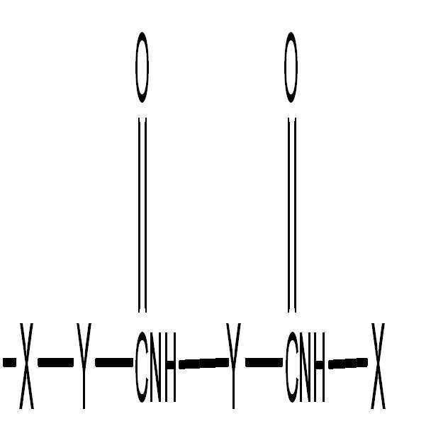

상기 화학식 2에서, m은 30 내지 1000의 정수이고, R1 및 R2는 메틸이다.
A solution of a diblock copolymer containing a crystalline hard segment containing at least one repeating unit represented by the following formula (1) and an amorphous soft segment containing a (meth) acrylate-based repeating unit represented by the following formula (2) To form a thin film;
Forming a polymer thin film by subjecting the applied thin film to solvent aging or heat treatment at a melting point of the hard segment and a glass transition temperature of the soft segment, respectively;
Irradiating the polymer thin film with ultraviolet light to remove the soft segment; And
And performing reactive ion etching of the pattern target film using the polymer thin film from which the soft segment has been removed as a mask.
[Chemical Formula 1]
(2)
Wherein n is an integer from 5 to 600, R is hydrogen or methyl, and R 'is selected from the group consisting of X,
In Formula 2, m is an integer of 30 to 1000, and R 1 and R 2 are methyl.


The method of claim 1, wherein the Z is ortho-phenylene,
2. The method of claim 1, wherein R "is substituted at the ortho, meta or para position of the aromatic ring included in Z.
The method of claim 1, wherein the diblock copolymer has a number average molecular weight of 5000 to 200000.
The method of claim 1, wherein the soft segment has a number average molecular weight of 3000 to 100000.
2. The method of claim 1, wherein the diblock copolymer comprises 20 to 80 mole percent of the hard segment and 80 to 20 mole percent of the soft segment.
라디칼 개시제 및 RAFT 시약의 존재 하에, 화학식 3의 (메타)아크릴레이트계 단량체를 1종 이상 포함하는 반응물을 RAFT 중합하는 단계; 및
상기 중합 생성물 및 라디칼 개시제의 존재 하에, 화학식 4의 단량체를 1종 이상 포함하는 반응물을 RAFT 중합하는 단계를 포함하는 방법에 의해 제조되며,
화학식 4의 단량체는 극성 용매 내에서 복수회 재결정되고, 극성 용매 및 비극성 용매의 첨가에 의해 결정 성장되어 단결정 형태로 제조된 상태로, 상기 RAFT 중합에 사용되는 나노 패턴 형성 방법:
[화학식 3]

[화학식 4]

상기 화학식 3에서, R1 및 R2는 메틸이고,
상기 화학식 4에서, R은 수소 또는 메틸이고, R'는 X,


The method of claim 1, wherein the diblock copolymer comprises
RAFT polymerization of a reactant comprising at least one (meth) acrylate monomer of formula (3) in the presence of a radical initiator and a RAFT reagent; And
Comprising RAFT polymerizing a reactant comprising at least one monomer of formula (4) in the presence of said polymerization product and a radical initiator,
The monomer of formula (4) is recrystallized a plurality of times in a polar solvent and is crystal-grown by the addition of a polar solvent and a non-polar solvent, and is produced in a single crystal form,
(3)
[Chemical Formula 4]
In Formula 3, R 1 and R 2 are methyl,
Wherein R is hydrogen or methyl, and R 'is selected from the group consisting of X,
9. The method according to claim 8, wherein the method for producing a diblock copolymer further comprises precipitating the polymerization product in a non-solvent.
The method of claim 8, wherein the monomer of Formula 4 is selected from the group consisting of p-dodecyl phenyl acrylamide (DOPAM), p-tetradecyl phenyl acrylamide, TEPAM (P-dodecyl) naphthyl acrylamide (DONAM), paratetradecyl naphthylacrylamide (HEPAM), para-hexadecyl phenyl acrylamide (P-tetradecyl) naphthyl acrylamide, TENAM, p-hexadecyl naphthyl acrylamide, HENAM, p-dodecyl naphthyl acrylamide, azabenzenyl acrylamide, DOAZAM], p-tetradecyl azobenzenyl acrylamide, TEAZAM, p-hexadecyl azobenzenyl acrylamide, and N- (4- [3- (5- (4-dodecyl-phenylcarbamoyl) -pentyl-carbamoyl) -propyl) odecyl-phenylcarbamoyl) pentyl-carbamoyl) -propyl) phenyl acrylamide, DOPPPAM).
The method of claim 8, wherein the radical initiator is selected from the group consisting of azobisisobutyronitrile (AIBN), 2,2'-azobis-2,4-dimethylvaleronitrile wherein the at least one selected from the group consisting of benzoyl peroxide (BPO) and di-t-butyl peroxide (DTBP) is at least one selected from the group consisting of dimethylvaleronitrile, benzoyl peroxide and DTBP.
9. The method of claim 8, wherein the RAFT reagent is selected from the group consisting of S-1-dodecyl-S '- (?,?' -Dimethyl-? "- acetic acid) trithiocarbonate, cyanoisopropyldithiobenzoate, At least one member selected from the group consisting of benzoate, cumene phenyl thioacetate, 1-phenylethyl-1-phenyldithioacetate and 4-cyano-4- (thiobenzoylthio) Pattern formation method.
9. The process of claim 8, wherein the RAFT polymerization of formula (3) or (4) is carried out in a solvent selected from the group consisting of methylene chloride, 1,2-dichloroethane, chlorobenzene, dichlorobenzene, benzene, toluene, acetone, chloroform, tetrahydrofuran, dioxane, , Diglyme, dimethylformamide, dimethylsulfoxide, and dimethylacetamide. The method for forming nanopatterns according to claim 1,
The method of forming a nanopattern according to claim 8, wherein the polymerization product of the RAFT polymerization step of the formula (3) comprises a polymer having a RAFT reagent bound to both terminals of the polymer of the (meth) acrylate monomer of the formula (3).
10. The method according to claim 9, wherein the non-solvent comprises at least one selected from the group consisting of methanol, ethanol, n-propanol, isopropanol, ethylene glycol, n-hexane, cyclohexane, n-heptane and petroleum ether.
The method according to claim 1, wherein in the step of forming the polymer thin film, the applied thin film is aged in a mixed solvent of a nonpolar solvent and a polar solvent at room temperature for 4 to 96 hours, or the melting point of the hard segment and the soft segment Lt; RTI ID = 0.0 > 2-24 < / RTI > hours at a glass transition temperature.
The method of claim 1, wherein the removing the soft segment comprises: disposing the polymer thin film by irradiating ultraviolet light to decompose the soft segment; and removing the soft segment by acid treatment.
Applications Claiming Priority (2)
| Application Number | Priority Date | Filing Date | Title |
|---|---|---|---|
| KR1020110038029 | 2011-04-22 | ||
| KR20110038029 | 2011-04-22 |
Publications (2)
| Publication Number | Publication Date |
|---|---|
| KR20120119998A KR20120119998A (en) | 2012-11-01 |
| KR101545279B1 true KR101545279B1 (en) | 2015-08-20 |
Family
ID=47042003
Family Applications (1)
| Application Number | Title | Priority Date | Filing Date |
|---|---|---|---|
| KR1020120027392A KR101545279B1 (en) | 2011-04-22 | 2012-03-16 | vel Diblock Copolymer, Preparation Method Thereof, And Method Of Forming Nano Pattern Using The Same |
Country Status (4)
| Country | Link |
|---|---|
| US (1) | US9493588B2 (en) |
| KR (1) | KR101545279B1 (en) |
| CN (1) | CN103562245B (en) |
| WO (1) | WO2012144735A2 (en) |
Families Citing this family (38)
| Publication number | Priority date | Publication date | Assignee | Title |
|---|---|---|---|---|
| KR101529646B1 (en) | 2012-09-10 | 2015-06-17 | 주식회사 엘지화학 | Method of forming silicon oxide nano pattern, metal nano pattern and magnetic patterned media for information storage |
| KR101490405B1 (en) | 2012-10-19 | 2015-02-06 | 주식회사 엘지화학 | Forming method of metal nano-structure of metal nano-wire pattern or metal nano-mesh pattern |
| JP5607187B2 (en) * | 2013-01-15 | 2014-10-15 | 東海ゴム工業株式会社 | Conductive material, method for manufacturing the same, and transducer using the same |
| KR101595034B1 (en) * | 2013-01-16 | 2016-02-17 | 주식회사 엘지화학 | Ultraviolet ray blocking film, acrylamide based compound and polymer included therein |
| US20140273290A1 (en) * | 2013-03-15 | 2014-09-18 | Tokyo Electron Limited | Solvent anneal processing for directed-self assembly applications |
| EP3078686B1 (en) | 2013-12-06 | 2018-10-31 | LG Chem, Ltd. | Block copolymer |
| JP6402867B2 (en) | 2013-12-06 | 2018-10-10 | エルジー・ケム・リミテッド | Block copolymer |
| US10202480B2 (en) | 2013-12-06 | 2019-02-12 | Lg Chem, Ltd. | Block copolymer |
| JP6521975B2 (en) * | 2013-12-06 | 2019-05-29 | エルジー・ケム・リミテッド | Block copolymer |
| JP6410327B2 (en) * | 2013-12-06 | 2018-10-24 | エルジー・ケム・リミテッド | Block copolymer |
| CN105899557B (en) * | 2013-12-06 | 2018-10-26 | 株式会社Lg化学 | Block copolymer |
| EP3078691B1 (en) * | 2013-12-06 | 2018-04-18 | LG Chem, Ltd. | Block copolymer |
| CN105899558B (en) * | 2013-12-06 | 2018-09-18 | 株式会社Lg化学 | Block copolymer |
| JP6496318B2 (en) * | 2013-12-06 | 2019-04-03 | エルジー・ケム・リミテッド | Block copolymer |
| JP6483694B2 (en) * | 2013-12-06 | 2019-03-13 | エルジー・ケム・リミテッド | Monomers and block copolymers |
| WO2015084122A1 (en) | 2013-12-06 | 2015-06-11 | 주식회사 엘지화학 | Block copolymer |
| CN105934456B (en) * | 2013-12-06 | 2018-09-28 | 株式会社Lg化学 | Block copolymer |
| EP3078693B1 (en) | 2013-12-06 | 2021-01-27 | LG Chem, Ltd. | Block copolymer |
| JP6419820B2 (en) * | 2013-12-06 | 2018-11-07 | エルジー・ケム・リミテッド | Block copolymer |
| FR3014888B1 (en) * | 2013-12-13 | 2017-05-26 | Arkema France | PROCESS FOR CREATING NANOMETRIC STRUCTURES BY SELF-ASSEMBLING BLOCK COPOLYMERS |
| KR101674972B1 (en) | 2013-12-26 | 2016-11-10 | 한국과학기술원 | Formation method of nano scale patterning and intergrated device for electronic apparatus manufacturing thereof |
| EP3214102B1 (en) | 2014-09-30 | 2022-01-05 | LG Chem, Ltd. | Block copolymer |
| JP6532941B2 (en) | 2014-09-30 | 2019-06-19 | エルジー・ケム・リミテッド | Block copolymer |
| US10633533B2 (en) | 2014-09-30 | 2020-04-28 | Lg Chem, Ltd. | Block copolymer |
| JP6451966B2 (en) | 2014-09-30 | 2019-01-16 | エルジー・ケム・リミテッド | Block copolymer |
| CN107075054B (en) * | 2014-09-30 | 2020-05-05 | 株式会社Lg化学 | Block copolymer |
| JP6394798B2 (en) | 2014-09-30 | 2018-09-26 | エルジー・ケム・リミテッド | Block copolymer |
| CN107078026B (en) | 2014-09-30 | 2020-03-27 | 株式会社Lg化学 | Method for preparing patterned substrate |
| CN107075052B (en) * | 2014-09-30 | 2020-05-29 | 株式会社Lg化学 | Block copolymer |
| US10287429B2 (en) | 2014-09-30 | 2019-05-14 | Lg Chem, Ltd. | Block copolymer |
| JP6633062B2 (en) | 2014-09-30 | 2020-01-22 | エルジー・ケム・リミテッド | Manufacturing method of patterned substrate |
| US10259907B2 (en) * | 2015-02-20 | 2019-04-16 | Az Electronic Materials (Luxembourg) S.À R.L. | Block copolymers with surface-active junction groups, compositions and processes thereof |
| KR101985802B1 (en) | 2015-06-11 | 2019-06-04 | 주식회사 엘지화학 | Laminate |
| TWI694140B (en) * | 2015-07-17 | 2020-05-21 | 日商捷恩智股份有限公司 | Polymerizable polar compound, liquid crystal composition and liquid crystal display element |
| KR102063054B1 (en) * | 2016-10-19 | 2020-01-07 | 주식회사 엘지화학 | Block copolymer containing photo-sensitive moiety |
| KR102183698B1 (en) | 2016-11-30 | 2020-11-26 | 주식회사 엘지화학 | Preparation method for polymer layer |
| FR3096369B1 (en) * | 2019-05-24 | 2022-01-14 | Arkema France | Process for polymerizing a composition in the presence of block copolymer |
| CN110116217B (en) * | 2019-05-28 | 2022-03-11 | 郑州大学 | Method for constructing two-dimensional gold nanoparticle pattern |
Citations (1)
| Publication number | Priority date | Publication date | Assignee | Title |
|---|---|---|---|---|
| JP2007125699A (en) | 2005-11-01 | 2007-05-24 | Hitachi Ltd | Pattern substrate, its manufacturing method, fine mold and magnetic recording pattern medium |
Family Cites Families (11)
| Publication number | Priority date | Publication date | Assignee | Title |
|---|---|---|---|---|
| US20110097559A1 (en) * | 1999-03-30 | 2011-04-28 | Hawker Craig J | Supramolecular block copolymer compositions for sub-micron lithography |
| KR100541748B1 (en) | 2003-12-10 | 2006-01-11 | 주식회사 엘지화학 | Acrylamides Monomer and Thermoresponsive Acrylamides Polymer Prepared by Using Same |
| US8133534B2 (en) * | 2004-11-22 | 2012-03-13 | Wisconsin Alumni Research Foundation | Methods and compositions for forming patterns with isolated or discrete features using block copolymer materials |
| US20060249784A1 (en) * | 2005-05-06 | 2006-11-09 | International Business Machines Corporation | Field effect transistor device including an array of channel elements and methods for forming |
| US20080038467A1 (en) * | 2006-08-11 | 2008-02-14 | Eastman Kodak Company | Nanostructured pattern method of manufacture |
| US8394483B2 (en) * | 2007-01-24 | 2013-03-12 | Micron Technology, Inc. | Two-dimensional arrays of holes with sub-lithographic diameters formed by block copolymer self-assembly |
| US8518837B2 (en) * | 2008-09-25 | 2013-08-27 | The University Of Massachusetts | Method of producing nanopatterned articles using surface-reconstructed block copolymer films |
| US8309278B2 (en) * | 2010-07-07 | 2012-11-13 | Massachusetts Institute Of Technology | Guided self-assembly of block copolymer line structures for integrated circuit interconnects |
| US9449822B2 (en) * | 2010-07-29 | 2016-09-20 | GlobalFoundries, Inc. | Method of forming semiconductor structures with contact holes |
| KR101529646B1 (en) * | 2012-09-10 | 2015-06-17 | 주식회사 엘지화학 | Method of forming silicon oxide nano pattern, metal nano pattern and magnetic patterned media for information storage |
| KR101490405B1 (en) * | 2012-10-19 | 2015-02-06 | 주식회사 엘지화학 | Forming method of metal nano-structure of metal nano-wire pattern or metal nano-mesh pattern |
-
2012
- 2012-03-16 KR KR1020120027392A patent/KR101545279B1/en active IP Right Grant
- 2012-03-16 CN CN201280019810.0A patent/CN103562245B/en active Active
- 2012-03-16 US US13/992,604 patent/US9493588B2/en active Active
- 2012-03-16 WO PCT/KR2012/001927 patent/WO2012144735A2/en active Application Filing
Patent Citations (1)
| Publication number | Priority date | Publication date | Assignee | Title |
|---|---|---|---|---|
| JP2007125699A (en) | 2005-11-01 | 2007-05-24 | Hitachi Ltd | Pattern substrate, its manufacturing method, fine mold and magnetic recording pattern medium |
Non-Patent Citations (2)
| Title |
|---|
| 이제권, 한양대학교 석사 논문, 2008년.* |
| 한국고분자학회, 2009년, 춘계 학술대회 발표 논문집, Vol. 34, No. 1.* |
Also Published As
| Publication number | Publication date |
|---|---|
| CN103562245A (en) | 2014-02-05 |
| KR20120119998A (en) | 2012-11-01 |
| WO2012144735A3 (en) | 2013-01-03 |
| US20130248488A1 (en) | 2013-09-26 |
| CN103562245B (en) | 2015-11-25 |
| WO2012144735A2 (en) | 2012-10-26 |
| US9493588B2 (en) | 2016-11-15 |
Similar Documents
| Publication | Publication Date | Title |
|---|---|---|
| KR101545279B1 (en) | vel Diblock Copolymer, Preparation Method Thereof, And Method Of Forming Nano Pattern Using The Same | |
| US9495991B2 (en) | Method for forming silicon oxide and metal nanopattern's, and magnetic recording medium for information storage using the same | |
| TWI586691B (en) | Block copolymer | |
| JP6637495B2 (en) | Manufacturing method of patterned substrate | |
| KR101756539B1 (en) | Preparation method of patterened substrate | |
| JP6361893B2 (en) | Block copolymer | |
| JP6347356B2 (en) | Block copolymer | |
| US9957363B2 (en) | Method for forming metal nanowire or metal nanomesh | |
| JP2017531709A (en) | Block copolymer | |
| JP2017501261A (en) | Block copolymer | |
| JP2017501267A (en) | Block copolymer | |
| TWI649343B (en) | Polymer composition | |
| TWI638838B (en) | Method for producing polymer film | |
| KR102096270B1 (en) | Compositon for neural layer | |
| KR102277770B1 (en) | Method for planarization of block copolymer layer and method for forming pattern | |
| TW201919886A (en) | Laminate | |
| KR20200020257A (en) | Compositon for neural layer |
Legal Events
| Date | Code | Title | Description |
|---|---|---|---|
| A201 | Request for examination | ||
| E902 | Notification of reason for refusal | ||
| E902 | Notification of reason for refusal | ||
| E701 | Decision to grant or registration of patent right | ||
| GRNT | Written decision to grant | ||
| FPAY | Annual fee payment |
Payment date: 20180619 Year of fee payment: 4 |