KR101533014B1 - Electrostatic clamp, lithographic apparatus and method of manufacturing an electrostatic clamp - Google Patents
Electrostatic clamp, lithographic apparatus and method of manufacturing an electrostatic clamp Download PDFInfo
- Publication number
- KR101533014B1 KR101533014B1 KR1020107008658A KR20107008658A KR101533014B1 KR 101533014 B1 KR101533014 B1 KR 101533014B1 KR 1020107008658 A KR1020107008658 A KR 1020107008658A KR 20107008658 A KR20107008658 A KR 20107008658A KR 101533014 B1 KR101533014 B1 KR 101533014B1
- Authority
- KR
- South Korea
- Prior art keywords
- burls
- support
- clamp
- lithographic apparatus
- electrostatic
- Prior art date
Links
Images


Classifications
-
- H—ELECTRICITY
- H01—ELECTRIC ELEMENTS
- H01L—SEMICONDUCTOR DEVICES NOT COVERED BY CLASS H10
- H01L21/00—Processes or apparatus adapted for the manufacture or treatment of semiconductor or solid state devices or of parts thereof
- H01L21/67—Apparatus specially adapted for handling semiconductor or electric solid state devices during manufacture or treatment thereof; Apparatus specially adapted for handling wafers during manufacture or treatment of semiconductor or electric solid state devices or components ; Apparatus not specifically provided for elsewhere
- H01L21/683—Apparatus specially adapted for handling semiconductor or electric solid state devices during manufacture or treatment thereof; Apparatus specially adapted for handling wafers during manufacture or treatment of semiconductor or electric solid state devices or components ; Apparatus not specifically provided for elsewhere for supporting or gripping
- H01L21/687—Apparatus specially adapted for handling semiconductor or electric solid state devices during manufacture or treatment thereof; Apparatus specially adapted for handling wafers during manufacture or treatment of semiconductor or electric solid state devices or components ; Apparatus not specifically provided for elsewhere for supporting or gripping using mechanical means, e.g. chucks, clamps or pinches
-
- G—PHYSICS
- G03—PHOTOGRAPHY; CINEMATOGRAPHY; ANALOGOUS TECHNIQUES USING WAVES OTHER THAN OPTICAL WAVES; ELECTROGRAPHY; HOLOGRAPHY
- G03F—PHOTOMECHANICAL PRODUCTION OF TEXTURED OR PATTERNED SURFACES, e.g. FOR PRINTING, FOR PROCESSING OF SEMICONDUCTOR DEVICES; MATERIALS THEREFOR; ORIGINALS THEREFOR; APPARATUS SPECIALLY ADAPTED THEREFOR
- G03F7/00—Photomechanical, e.g. photolithographic, production of textured or patterned surfaces, e.g. printing surfaces; Materials therefor, e.g. comprising photoresists; Apparatus specially adapted therefor
- G03F7/70—Microphotolithographic exposure; Apparatus therefor
- G03F7/70691—Handling of masks or workpieces
- G03F7/707—Chucks, e.g. chucking or un-chucking operations or structural details
- G03F7/70708—Chucks, e.g. chucking or un-chucking operations or structural details being electrostatic; Electrostatically deformable vacuum chucks
-
- H—ELECTRICITY
- H01—ELECTRIC ELEMENTS
- H01L—SEMICONDUCTOR DEVICES NOT COVERED BY CLASS H10
- H01L21/00—Processes or apparatus adapted for the manufacture or treatment of semiconductor or solid state devices or of parts thereof
- H01L21/02—Manufacture or treatment of semiconductor devices or of parts thereof
- H01L21/027—Making masks on semiconductor bodies for further photolithographic processing not provided for in group H01L21/18 or H01L21/34
-
- H—ELECTRICITY
- H01—ELECTRIC ELEMENTS
- H01L—SEMICONDUCTOR DEVICES NOT COVERED BY CLASS H10
- H01L21/00—Processes or apparatus adapted for the manufacture or treatment of semiconductor or solid state devices or of parts thereof
- H01L21/67—Apparatus specially adapted for handling semiconductor or electric solid state devices during manufacture or treatment thereof; Apparatus specially adapted for handling wafers during manufacture or treatment of semiconductor or electric solid state devices or components ; Apparatus not specifically provided for elsewhere
- H01L21/683—Apparatus specially adapted for handling semiconductor or electric solid state devices during manufacture or treatment thereof; Apparatus specially adapted for handling wafers during manufacture or treatment of semiconductor or electric solid state devices or components ; Apparatus not specifically provided for elsewhere for supporting or gripping
- H01L21/6831—Apparatus specially adapted for handling semiconductor or electric solid state devices during manufacture or treatment thereof; Apparatus specially adapted for handling wafers during manufacture or treatment of semiconductor or electric solid state devices or components ; Apparatus not specifically provided for elsewhere for supporting or gripping using electrostatic chucks
-
- H—ELECTRICITY
- H01—ELECTRIC ELEMENTS
- H01L—SEMICONDUCTOR DEVICES NOT COVERED BY CLASS H10
- H01L21/00—Processes or apparatus adapted for the manufacture or treatment of semiconductor or solid state devices or of parts thereof
- H01L21/67—Apparatus specially adapted for handling semiconductor or electric solid state devices during manufacture or treatment thereof; Apparatus specially adapted for handling wafers during manufacture or treatment of semiconductor or electric solid state devices or components ; Apparatus not specifically provided for elsewhere
- H01L21/683—Apparatus specially adapted for handling semiconductor or electric solid state devices during manufacture or treatment thereof; Apparatus specially adapted for handling wafers during manufacture or treatment of semiconductor or electric solid state devices or components ; Apparatus not specifically provided for elsewhere for supporting or gripping
- H01L21/687—Apparatus specially adapted for handling semiconductor or electric solid state devices during manufacture or treatment thereof; Apparatus specially adapted for handling wafers during manufacture or treatment of semiconductor or electric solid state devices or components ; Apparatus not specifically provided for elsewhere for supporting or gripping using mechanical means, e.g. chucks, clamps or pinches
- H01L21/68714—Apparatus specially adapted for handling semiconductor or electric solid state devices during manufacture or treatment thereof; Apparatus specially adapted for handling wafers during manufacture or treatment of semiconductor or electric solid state devices or components ; Apparatus not specifically provided for elsewhere for supporting or gripping using mechanical means, e.g. chucks, clamps or pinches the wafers being placed on a susceptor, stage or support
- H01L21/6875—Apparatus specially adapted for handling semiconductor or electric solid state devices during manufacture or treatment thereof; Apparatus specially adapted for handling wafers during manufacture or treatment of semiconductor or electric solid state devices or components ; Apparatus not specifically provided for elsewhere for supporting or gripping using mechanical means, e.g. chucks, clamps or pinches the wafers being placed on a susceptor, stage or support characterised by a plurality of individual support members, e.g. support posts or protrusions
-
- H—ELECTRICITY
- H02—GENERATION; CONVERSION OR DISTRIBUTION OF ELECTRIC POWER
- H02N—ELECTRIC MACHINES NOT OTHERWISE PROVIDED FOR
- H02N13/00—Clutches or holding devices using electrostatic attraction, e.g. using Johnson-Rahbek effect
Landscapes
- Engineering & Computer Science (AREA)
- Physics & Mathematics (AREA)
- General Physics & Mathematics (AREA)
- Condensed Matter Physics & Semiconductors (AREA)
- Manufacturing & Machinery (AREA)
- Computer Hardware Design (AREA)
- Microelectronics & Electronic Packaging (AREA)
- Power Engineering (AREA)
- Exposure And Positioning Against Photoresist Photosensitive Materials (AREA)
- Container, Conveyance, Adherence, Positioning, Of Wafer (AREA)
- Jigs For Machine Tools (AREA)
Abstract
본 발명은 버얼들이 제공된 물질 층을 포함하는 리소그래피 장치에서 사용하기 위한 정전기 클램프 - 절연체 및/또는 유전 물질에 의해 둘러싸인 전극이 상기 버얼들 사이에 제공됨 -, 및 이러한 정전기 클램프를 제조하는 방법에 관한 것이다. 상기 정전기 클램프는 리소그래피 장치에서 대상물 지지체에 대해 대상물을 클램핑하는 데 사용될 수 있다.The present invention relates to an electrostatic clamp-insulator and / or an electrode surrounded by a dielectric material for use in a lithographic apparatus comprising a layer of material provided with burls, and to a method of manufacturing such an electrostatic clamp . The electrostatic clamp may be used to clamp an object against an object support in a lithographic apparatus.
Description
본 발명은 사용 시 리소그래피 장치 내의 고정된 평면에 대상물(object)(예를 들어, 웨이퍼, 기판 또는 레티클)을 유지하는 정전기 클램프에 관한 것으로, 상기 클램프는 버얼(burl)들이 제공된 지지체를 포함하며, 상기 버얼들의 최상부는 대상물이 유지되는 평면을 결정하고, 절연체에 의해 둘러싸인 전극이 상기 버얼들 사이에 제공된다.The present invention relates to an electrostatic clamp for holding an object (e.g. a wafer, a substrate or a reticle) in a fixed plane in use in a lithographic apparatus, said clamp comprising a support provided with burls, The top of the burls determines the plane in which the object is held, and an electrode surrounded by an insulator is provided between the burls.
리소그래피 장치는 기판 상에, 통상적으로는 기판의 타겟부 상에 원하는 패턴을 적용시키는 기계이다. 리소그래피 장치는, 예를 들어 집적 회로(IC)의 제조시에 사용될 수 있다. 그 경우에, 패터닝 디바이스, 예를 들어 마스크(레티클)가 IC의 개별층 상에 형성될 회로 패턴을 생성하기 위해 사용될 수 있다. 이 패턴은 기판(예컨대, 실리콘 웨이퍼) 상의 (예를 들어, 다이의 일부, 한 개 또는 수 개의 다이를 포함하는) 타겟부 상으로 전사(transfer)될 수 있다. 패턴의 전사는, 통상적으로 기판상에 제공된 방사선-감응재(레지스트)층 상으로의 이미징(imaging)을 통해 수행된다. 일반적으로, 단일 기판은 연속하여 패터닝되는 인접한 타겟부들의 네트워크를 포함할 것이다.A lithographic apparatus is a machine that applies a desired pattern onto a substrate, typically onto a target portion of the substrate. The lithographic apparatus may be used, for example, in the manufacture of integrated circuits (ICs). In that case, a patterning device, for example a mask (reticle), may be used to create a circuit pattern to be formed on an individual layer of the IC. This pattern can be transferred onto a target portion (e.g. comprising part of a die, including one or several dies) on a substrate (e.g. a silicon wafer). The transfer of the pattern is typically performed through imaging onto a layer of radiation-sensitive material (resist) provided on the substrate. In general, a single substrate will comprise a network of adjacent target portions that are successively patterned.
정전기 클램프들은 소정 파장들, 예를 들어 EUV에서 작동하는 리소그래피 장치들에 사용될 수 있는데, 이는 이러한 파장들에서 리소그래피 장치의 몇몇 영역들이 진공 조건들 하에서 작동하기 때문이다. 마스크 또는 기판(웨이퍼)과 같은 대상물을, 각각 마스크 테이블 또는 웨이퍼 테이블과 같은 대상물 지지체에 대해 정전기적으로 클램핑하기 위해, 정전기 클램프가 사용될 수 있다. 정전기 클램프는 사전-정렬 유닛(pre-alignment unit)에서 대상물을 정전기적으로 클램핑하는 데 사용될 수 있다.Electrostatic clamps can be used in lithographic apparatuses operating at certain wavelengths, e.g. EUV, because at these wavelengths several regions of the lithographic apparatus operate under vacuum conditions. An electrostatic clamp can be used to electrostatically clamp an object such as a mask or substrate (wafer) to an object support such as a mask table or a wafer table, respectively. The electrostatic clamp can be used to electrostatically clamp an object in a pre-alignment unit.
US 4,502,094호(도 2 및 도 3)는, 예를 들어 알루미늄으로 만들어진 열 전도성 지지체(3, 5)를 포함하는 정전기 척(electrostatic chuck: 클램프)(2) 상에 위치된 반도체 웨이퍼(1)를 개시한다. 상기 척 상에 웨이퍼(1)를 위치시키기 위해, 웨이퍼(1)의 평평한 에지(1a)가 핀들(13a)과 접할 수 있고 둥근 에지(1b)가 핀(13b)과 접하도록 위치 핀들(locating pins; 13a, 13b)이 제공되어, 웨이퍼(1)의 위치가 유일하게(uniquely) 정의된다. 상기 지지체는 두께가 6 mm일 수 있는 외주 부분(3) 및 약 3.5 mm의 두께를 갖는 더 얇은 관통된(perforated) 중심 부분(5)을 갖는다. 상기 중심 부분은 3 mm의 직경을 갖는, 단면이 원형인 관통부들 또는 어퍼처들(6)을 갖는다. 또한, 정전기 척(2)은 어퍼처들(6) 내에 고정된 구리 필러(pillar: 7)들의 형태로 된 열 전도성 부분들을 포함한다. 길이가 6 mm이고 3 mm의 직경을 갖는 상기 필러들(7)은 지지체의 중심 부분과, 그리고 외주 부분(3)[이는 비교적 큰 크기로 인해 히트 싱크(heat sink)로서 기능할 수 있음]과 열 접촉한다.US 4,502,094 (Figures 2 and 3) discloses a process for producing a
상기 필러들(7)은 고정된 동일 평면에 놓인 평탄한 단부면들(8)을 가지므로, 반도체 웨이퍼(1)는 상기 단부면들 뿐만 아니라 상기 지지체의 외주 부분(3)의 주요 표면(9) 상에서 지탱될 수 있다. 이러한 방식으로, 정전기 척(2)에 대해 고정된 평면에서 웨이퍼가 지지될 수 있다. 또한, 필러들(7)은 금속으로 만들어지기 때문에, 반도체 웨이퍼(1)가 상기 필러들(7)에 의해 그 후방면[즉, 정전기 척(2)을 향해 있는 표면]에서 전기 접촉되도록 전기적으로(또한, 열적으로) 전도성이다.The
또한, 상기 척(2)은, 예를 들어 알루미늄으로 만들어질 수 있는 그리드 전극(grid electrode: 10)의 형태로 된 전기 전도성 부재를 갖는다. 본질적으로, 상기 그리드(10)는 원형이며, 90 nm의 직경과 1.3 mm의 두께를 갖는다. 상기 그리드(10)의 메시(mesh)들은 5 mm의 직경을 갖는 원형 어퍼처들(11)에 의해 구성된다. 상기 그리드(10)는 필러들(7) 사이로 연장되는 부분들을 갖는데, 이는 필러들(7)이 어퍼처들(11)을 통해 연장되지만, 상기 필러들(7) 및 그리드(10)는 유전 물질 층(12)에 의해 서로 절연되도록 위치되기 때문이다. 예를 들어, 에폭시 수지일 수 있는 상기 유전 물질 층(12)은, 상기 필러들(7)로부터 그리드를 절연시키는 것 이외에도, 상기 그리드(10)가 지지체의 중심 부분(5)으로부터도 절연되도록 상기 그리드(10)를 둘러싼다. 지지체(2)의 중심 부분(5)과 필러들(7) 둘 모두로부터의 그리드(10)의 간격은, 예를 들어 1 mm이며, 유전 층(10)은 이러한 다양한 부재들 사이의 전체 공간을 채운다. 또한, 유전 층은 그리드(10)의 상부 표면 상에 존재하지만, 상기 층(10)의 이 부분은 약 200 ㎛의 두께를 갖는다. 이후에 더 자세히 설명되는 바와 같이, 반도체 웨이퍼(1)가 유전 층(12)으로부터 약 10 ㎛ 이격되도록, 필러들(7)이 상기 층(12)으로부터 돌출될 수도 있다.Further, the
척(2)에 대해 반도체 웨이퍼(1)를 유지하기 위하여, 상기 웨이퍼(1)와 그리드 전극(10) 사이에 전위차가 인가된다. 통상적으로, 이 전위차는 4 kV이다. 필러들(7)을 통해 지지체(2)로부터 웨이퍼(1)의 뒷면에 전기적인 접촉이 행해지며, 지지체의 중심 부분(5)을 통해 그리고 유전 층(12)을 통해 연장되는 전기 연결부(4)를 통해 예를 들어 약 4 kV의 바이어스 전위가 그리드(10)에 인가된다. 따라서, 웨이퍼(1)가 척(2)의 필러들(7)에 대해 고정된 평면에서 유지되도록 상기 유전 층(12)에 걸쳐 정전기 클램핑력이 조성된다. 상기 클램핑력의 크기는 웨이퍼(1)와 전극(10) 사이의 전위차의 제곱(square)에 비례하고, 상기 층(12)의 유전 상수에 직접적으로 비례하며, 웨이퍼(1)와 그리드(10) 사이의 거리의 제곱에 반비례한다.A potential difference is applied between the
도 3은 반도체 웨이퍼가 부분적으로 절단된, 도 2의 척 및 반도체 웨이퍼를 위에서 본 평면도이다. 도 2는 도 3의 라인 I-I'을 따른 단면도를 도시한다. 도 3에 도시된 바와 같이, 척(2)은 필러들(7)의 대칭적인 분포를 갖는다. 웨이퍼가 척에 대해 고르게 유지되도록 하기 위해, 웨이퍼의 국부화된 휨(localized bowing)을 회피하도록 필러들(7)이 비교적 가깝게 이격되는 것이 바람직하다. 또한, 이는 웨이퍼(1)에 걸친 온도 변동들을 회피하여야 할 필요성에도 부합된다. 필러들(7)의 개수가 더 많고, 그 간격이 더 가까워질수록, 웨이퍼로부터 지지체의 두꺼운 외주 히트 싱크(3)로의 열 전달이 더 효율적일 수 있다. 하지만, 필러들의 개수가 관계되는 한, 필러들(7)의 개수가 증가됨에 따라 정전기 인력으로 인한 접촉 압력이 감소되기 때문에 절충이 이루어져야 한다. 하지만, 필러들(7)이 유전 층(12)으로부터 돌출되기 때문에, 웨이퍼(1)는 상기 필러들(7)의 단부면들(8)과 주요 평면(9)의 내주면에서만 척(2)과 접촉한다. 이러한 방식으로 접촉 면적을 제한함으로써, 접촉 압력(즉, 단위 면적당 힘)이 최대화된다. 이는 웨이퍼(1)와 필러들(7) 사이의 열 전달의 효율성이 접촉 압력에 의존하기 때문에 유익하다.Figure 3 is a top view of the chuck and semiconductor wafer of Figure 2, with the semiconductor wafer partially cut away. Figure 2 shows a cross-sectional view along line I-I 'of Figure 3. As shown in Fig. 3, the
정전기 클램프 상에 클램핑되는 대상물은 정전기 클램프 상에 매우 높은 정확도로 위치되어야 할 필요성이 있으며, 상기 정전기 클램프 상의 상기 대상물의 위치는 시간에 걸쳐 안정하게 유지되어야 한다.The object to be clamped on the electrostatic clamp needs to be positioned with very high accuracy on the electrostatic clamp, and the position of the object on the electrostatic clamp must remain stable over time.
예를 들어, 대상물의 위치의 높은 정확성 및 안정성을 제공하는 개선된 정전기 클램프를 제공하는 것이 유익할 것이다.For example, it would be advantageous to provide an improved electrostatic clamp that provides high accuracy and stability of the position of the object.
본 발명의 일 실시형태에 따르면, 사용 시 리소그래피 장치 내의 고정된 평면에서 대상물을 유지하는 정전기 클램프가 제공되고, 상기 클램프는 버얼들이 제공된 지지체를 포함하고, 상기 버얼들의 최상부는 상기 대상물이 유지되는 평면을 결정하며, 절연체에 의해 둘러싸인 전극이 상기 버얼들 사이에 제공되고, 상기 지지체는 낮은 팽창 물질로 만들어진다.According to an embodiment of the invention there is provided an electrostatic clamp for holding an object in a fixed plane in use in a lithographic apparatus in use, the clamp comprising a support on which burls are provided, An electrode surrounded by an insulator is provided between the burls, and the support is made of a low expansion material.
본 발명의 또 다른 실시형태에 따르면, 리소그래피 장치 내의 대상물 지지체에 대해 대상물을 정전기적으로 클램핑하도록 구성된 정전기 클램프를 제조하는 방법이 제공되고, 상기 방법은 버얼들을 갖는 물질 층을 제공하는 단계, 및 상기 버얼들 사이에 절연체 및/또는 유전 물질에 의해 둘러싸인 전극을 배치시키는 단계를 포함한다. 상기 제조 방법은 상기 절연체 및/또는 유전 물질을 제공하기 위해 스퍼터링 공정, 화학 기상 증착 공정 또는 이들의 조합을 이용하는 단계를 포함한다.According to another aspect of the present invention there is provided a method of fabricating an electrostatic clamp configured to electrostatically clamp an object against an object support in a lithographic apparatus, the method comprising: providing a layer of material with burls; And disposing electrodes surrounded by insulators and / or dielectric materials between the burls. The fabrication method includes using a sputtering process, a chemical vapor deposition process, or a combination thereof to provide the insulator and / or dielectric material.
본 발명의 또 다른 실시형태에 따르면, 방사선 빔의 빔 경로 내의 대상물을 지지하도록 구성된 대상물 지지체; 및 상기 대상물 지지체에 대해 상기 대상물을 정전기적으로 클램핑하도록 구성된 정전기 클램프를 포함하고, 상기 클램프는 버얼들이 제공된 지지체를 포함하고, 상기 버얼들의 최상부는 상기 대상물이 유지되는 평면을 결정하며, 절연체에 의해 둘러싸인 전극이 상기 버얼들 사이에 제공되고, 상기 지지체는 낮은 팽창 물질로 만들어진다.According to another embodiment of the present invention, there is provided a lithographic apparatus comprising: an object support configured to support an object in a beam path of a radiation beam; And an electrostatic clamp configured to electrostatically clamp the object relative to the object support, the clamp comprising a support on which burls are provided, the top of the burls defining a plane in which the object is held, An enclosed electrode is provided between the burls, and the support is made of a low expansion material.
이하, 대응하는 참조 부호들이 대응하는 부분들을 나타내는 첨부된 개략적인 도면들을 참조하여, 단지 예시의 방식으로만 본 발명의 실시예들을 설명할 것이다:
도 1은 본 발명의 일 실시예가 사용될 수 있는 리소그래피 장치를 도시한 도면;
도 2는 종래 기술에 따라 정전기 척상에 위치된 반도체 웨이퍼의 도 3의 라인 I--I'에 따른 단면도;
도 3은 도 2의 부분적으로 절단된 반도체 웨이퍼 및 척을 위에서 본 평면도;
도 4는 본 발명의 일 실시예에 따른 정전기 클램프의 최상부 층의 부분 단면도;
도 5는 본 발명의 또 다른 실시예에 따른 정전기 클램프의 최상부 층의 부분 단면도;
도 6은 또 다른 실시예에 따른 정전기 클램프의 평면도;
도 7은 도 6의 정전기 클램프의 단면도;
도 8은 정전기 클램프의 또 다른 실시예의 평면도이다.BRIEF DESCRIPTION OF THE DRAWINGS Embodiments of the invention will now be described, by way of example only, with reference to the accompanying schematic drawings in which corresponding reference symbols indicate corresponding parts:
1 illustrates a lithographic apparatus in which an embodiment of the present invention may be used;
Figure 2 is a cross-sectional view along line I-I 'of Figure 3 of a semiconductor wafer positioned on an electrostatic chuck in accordance with the prior art;
Figure 3 is a plan view of the partially cut semiconductor wafer and chuck of Figure 2 viewed from above;
4 is a partial cross-sectional view of an uppermost layer of an electrostatic clamp according to one embodiment of the present invention;
5 is a partial cross-sectional view of an uppermost layer of an electrostatic clamp according to another embodiment of the present invention;
6 is a plan view of an electrostatic clamp according to yet another embodiment;
Figure 7 is a cross-sectional view of the electrostatic clamp of Figure 6;
8 is a plan view of another embodiment of an electrostatic clamp.
도 1은 본 발명의 일 실시예에 따른 리소그래피 장치를 개략적으로 도시한다. 상기 장치는, 방사선 빔(B)(예를 들어, UV 방사선 또는 EUV 방사선)을 컨디셔닝하도록 구성된 조명 시스템(일루미네이터)(IL); 패터닝 디바이스(예를 들어, 마스크)(MA)를 지지하도록 구성되고, 소정 파라미터들에 따라 패터닝 디바이스를 정확히 위치시키도록 구성된 제 1 위치설정기(PM)에 연결된 지지 구조체(예를 들어, 마스크 테이블)(MT); 기판(예를 들어, 레지스트-코팅된 웨이퍼)(W)을 유지하도록 구성되고, 소정 파라미터들에 따라 기판을 정확히 위치시키도록 구성된 제 2 위치설정기(PW)에 연결된 기판 테이블(예를 들어, 웨이퍼 테이블)(WT); 및 기판(W)의 (예를 들어, 1 이상의 다이를 포함하는) 타겟부(C) 상으로 패터닝 디바이스(MA)에 의해 방사선 빔(B)에 부여된 패턴을 투영하도록 구성된 투영 시스템(예를 들어, 굴절 투영 렌즈 시스템)(PS)을 포함한다.Figure 1 schematically depicts a lithographic apparatus according to an embodiment of the invention. The apparatus comprises: an illumination system (illuminator) IL configured to condition a radiation beam B (e.g. UV radiation or EUV radiation); A support structure (e.g., a mask table) MA constructed to support a patterning device (e.g., mask) MA and coupled to a first positioner PM configured to accurately position the patterning device in accordance with certain parameters ) (MT); A substrate table (e.g., a wafer table) configured to hold a substrate (e.g., a resist-coated wafer) W and connected to a second positioner PW configured to accurately position the substrate according to certain parameters, Wafer table) WT; And a projection system (e.g., a projection system) configured to project a pattern imparted to the radiation beam B by a patterning device MA onto a target portion C (e.g. comprising one or more dies) For example, a refractive projection lens system (PS).
조명 시스템은 방사선을 지향, 성형, 또는 제어하기 위하여, 굴절, 반사, 자기, 전자기, 정전기 또는 다른 타입의 광학 구성요소들, 또는 여하한의 그 조합과 같은 다양한 타입들의 광학 구성요소들을 포함할 수 있다.The illumination system may include various types of optical components, such as refractive, reflective, magnetic, electromagnetic, electrostatic or other types of optical components, or any combination thereof, for directing, shaping, or controlling radiation have.
지지 구조체는 패터닝 디바이스를 지지, 즉 패터닝 디바이스의 무게를 견딘다. 이는 패터닝 디바이스의 방위, 리소그래피 장치의 디자인, 및 예를 들어 패터닝 디바이스가 진공 환경에서 유지되는지의 여부와 같은 다른 조건들에 의존하는 방식으로 패터닝 디바이스를 유지한다. 지지 구조체는 패터닝 디바이스를 유지하기 위해 기계적, 진공, 정전기, 또는 다른 클램핑 기술들을 이용할 수 있다. 지지 구조체는, 예를 들어 필요에 따라 고정되거나 이동가능할 수 있는 프레임 또는 테이블일 수 있다. 지지 구조체는, 패터닝 디바이스가 예를 들어 투영 시스템에 대해 원하는 위치에 있을 것을 보장할 수 있다. 본 명세서의 "레티클" 또는 "마스크"라는 용어의 어떠한 사용도 "패터닝 디바이스"라는 좀 더 일반적인 용어와 동의어로 간주될 수 있다.The support structure supports the patterning device, i. E., Weighs the weight of the patterning device. It holds the patterning device in a manner that depends on the orientation of the patterning device, the design of the lithographic apparatus, and other conditions, such as for example whether or not the patterning device is held in a vacuum environment. The support structure may utilize mechanical, vacuum, electrostatic, or other clamping techniques to hold the patterning device. The support structure may be, for example, a frame or a table that may be fixed or movable as required. The support structure can ensure that the patterning device is at a desired position, for example with respect to the projection system. Any use of the terms "reticle" or "mask" herein may be considered synonymous with the more general term "patterning device".
본 명세서에서 사용되는 "패터닝 디바이스"라는 용어는, 기판의 타겟부에 패턴을 생성하기 위해서, 방사선 빔의 단면에 패턴을 부여하는 데 사용될 수 있는 여하한의 디바이스를 언급하는 것으로 폭넓게 해석되어야 한다. 방사선 빔에 부여된 패턴은, 예를 들어 상기 패턴이 위상-시프팅 피처(phase-shifting feature)들 또는 소위 어시스트 피처(assist feature)들을 포함하는 경우, 기판의 타겟부 내의 원하는 패턴과 정확히 일치하지 않을 수도 있다는 것을 유의하여야 한다. 일반적으로, 방사선 빔에 부여된 패턴은 집적 회로와 같이 타겟부에 생성될 디바이스 내의 특정 기능 층에 해당할 것이다.The term "patterning device " as used herein should be broadly interpreted as referring to any device that can be used to impart a pattern to a cross-section of a radiation beam in order to create a pattern in a target portion of the substrate. The pattern imparted to the radiation beam may be precisely matched to the desired pattern in the target portion of the substrate, for example when the pattern comprises phase-shifting features or so-called assist features . Generally, the pattern imparted to the radiation beam will correspond to a particular functional layer in the device to be created in the target portion, such as an integrated circuit.
패터닝 디바이스는 투과형 또는 반사형일 수 있다. 패터닝 디바이스의 예로는 마스크, 프로그램가능한 거울 어레이 및 프로그램가능한 LCD 패널들을 포함한다. 마스크는 리소그래피 분야에서 잘 알려져 있으며, 바이너리(binary)형, 교번 위상-시프트형 및 감쇠 위상-시프트형과 같은 마스크 타입뿐만 아니라, 다양한 하이브리드(hybrid) 마스크 타입들을 포함한다. 프로그램가능한 거울 어레이의 일 예시는 작은 거울들의 매트릭스 구성을 채택하며, 그 각각은 입사하는 방사선 빔을 상이한 방향으로 반사시키도록 개별적으로 기울어질 수 있다. 기울어진 거울들은 거울 매트릭스에 의해 반사되는 방사선 빔에 패턴을 부여한다.The patterning device may be transmissive or reflective. Examples of patterning devices include masks, programmable mirror arrays, and programmable LCD panels. Masks are well known in the lithographic arts and include various types of hybrid masks as well as mask types such as binary, alternating phase-shift and attenuated phase-shift types. One example of a programmable mirror array employs a matrix configuration of small mirrors, each of which can be individually tilted to reflect an incoming radiation beam in different directions. The tilted mirrors impart a pattern to the radiation beam reflected by the mirror matrix.
본 명세서에서 사용되는 "투영 시스템"이라는 용어는, 사용되는 노광 방사선에 대하여, 또는 침지 액체의 사용 또는 진공의 사용과 같은 다른 인자들에 대하여 적절하다면, 굴절, 반사, 카타디옵트릭(catadioptric), 자기, 전자기 및 정전기 광학 시스템, 또는 여하한의 그 조합을 포함하는 여하한 타입의 투영 시스템을 포괄하는 것으로서 폭넓게 해석되어야 한다. 본 명세서의 "투영 렌즈"라는 용어의 어떠한 사용도 "투영 시스템"이라는 좀 더 일반적인 용어와 동의어로 간주될 수 있다.The term "projection system " used herein should be broadly interpreted as encompassing any type of projection system, including refractive, reflective, catadioptric, catadioptric, catadioptric, But should be broadly interpreted as encompassing any type of projection system, including magnetic, electromagnetic and electrostatic optical systems, or any combination thereof. Any use of the term "projection lens" herein may be considered as synonymous with the more general term "projection system ".
또한, 지지 구조체 및 기판 테이블은 이후 아티클 지지체(article support)라고 언급될 수도 있다. 아티클은, 제한하는 것은 아니지만, 레티클과 같은 패터닝 디바이스 및 웨이퍼와 같은 기판을 포함한다.In addition, the support structure and the substrate table may hereinafter also be referred to as article supports. Articles include, but are not limited to, a patterning device, such as a reticle, and a substrate, such as a wafer.
본 명세서에 도시된 바와 같이, 상기 장치는 (예를 들어, 반사 마스크를 채택하는) 반사형으로 구성된다. 대안적으로, 상기 장치는 (예를 들어, 투과 마스크를 채택하는) 투과형으로 구성될 수 있다.As here depicted, the apparatus is of a reflective type (e.g. employing a reflective mask). Alternatively, the apparatus may be of a transmissive type (e.g. employing a transmissive mask).
리소그래피 장치는 2 개(듀얼 스테이지) 이상의 기판 테이블(및/또는 2 이상의 마스크 테이블)을 갖는 형태로 구성될 수 있다. 이러한 "다수 스테이지" 기계에서는 추가 테이블이 병행하여 사용될 수 있으며, 또는 1 이상의 테이블이 노광에 사용되고 있는 동안 1 이상의 다른 테이블에서는 준비작업 단계가 수행될 수 있다.The lithographic apparatus may be of a type having two (dual stage) or more substrate tables (and / or two or more mask tables). In such "multiple stage" machines additional tables may be used in parallel, or preparatory steps may be carried out on one or more tables while one or more tables are being used for exposure.
또한, 리소그래피 장치(100)는 투영 시스템과 기판 사이의 공간을 채우기 위해서, 기판의 전체 또는 일부분이 비교적 높은 굴절률을 갖는 액체, 예컨대 물로 덮일 수 있는 형태로도 구성될 수 있다. 또한, 침지 액체는 리소그래피 장치 내의 다른 공간들, 예를 들어 마스크와 투영 시스템 사이에도 적용될 수 있다. 침지 기술은 투영 시스템의 개구수(numerical aperture)를 증가시키는 것으로 당업계에 잘 알려져 있다. 본 명세서에서 사용되는 "침지"라는 용어는 기판과 같은 구조체가 액체에 담그어져야 함을 의미하는 것이라기보다는, 노광시 액체가 투영 시스템과 기판 사이에 놓이기만 하면 된다는 것을 의미한다.The lithographic apparatus 100 may also be configured in such a way that all or a portion of the substrate may be covered with a liquid, e.g., water, having a relatively high refractive index, to fill the space between the projection system and the substrate. Immersion liquid may also be applied to other spaces in the lithographic apparatus, for example, between the mask and the projection system. Immersion techniques are well known in the art for increasing the numerical aperture of a projection system. As used herein, the term "immersion " does not mean that a structure such as a substrate has to be immersed in the liquid, but rather means that the liquid only has to lie between the projection system and the substrate during exposure.
도 1을 참조하면, 일루미네이터(IL)는 방사선 소스(SO)로부터 방사선 빔을 수용한다. 예를 들어, 상기 소스가 엑시머 레이저(excimer laser)인 경우, 상기 소스 및 리소그래피 장치는 별도의 개체일 수 있다. 이러한 경우, 상기 소스는 리소그래피 장치의 일부분을 형성하는 것으로 간주되지 않으며, 상기 방사선 빔은 예를 들어 적절한 지향 거울 및/또는 빔 익스팬더(beam expander)를 포함하는 빔 전달 시스템의 도움으로, 소스(SO)로부터 일루미네이터(IL)로 통과된다. 다른 경우들에서, 예를 들어 상기 소스가 수은 램프인 경우, 상기 소스는 리소그래피 장치의 통합부일 수 있다. 상기 소스(SO) 및 일루미네이터(IL)는, 필요에 따라 빔 전달 시스템과 함께 방사선 시스템이라고도 칭해질 수 있다.Referring to Figure 1, the illuminator IL receives a radiation beam from a radiation source SO. For example, where the source is an excimer laser, the source and the lithographic apparatus may be separate entities. In such a case, the source is not considered to form part of the lithographic apparatus, and the radiation beam is incident on the source (SO) with the aid of a beam delivery system including, for example, a suitable directing mirror and / or a beam expander. To the illuminator IL. In other cases, for example when the source is a mercury lamp, the source may be an integral part of the lithographic apparatus. The source SO and the illuminator IL may also be referred to as a radiation system together with a beam delivery system if necessary.
상기 일루미네이터(IL)는 방사선 빔의 각도 세기 분포를 조정하는 조정기를 포함할 수 있다. 일반적으로, 일루미네이터의 퓨필 평면 내의 세기 분포의 적어도 외반경 및/또는 내반경 크기(통상적으로, 각각 외측-σ 및 내측-σ라 함)가 조정될 수 있다. 또한, 일루미네이터(IL)는 인티그레이터 및 콘덴서와 같이, 다양한 다른 구성요소들을 포함할 수도 있다. 일루미네이터는 방사선 빔의 단면이 원하는 균일성(uniformity) 및 세기 분포를 갖도록, 방사선 빔을 컨디셔닝하는 데 사용될 수 있다.The illuminator IL may comprise an adjuster for adjusting the angular intensity distribution of the radiation beam. Generally, at least the outer and / or inner radial extent (commonly referred to as -outer and -inner, respectively) of the intensity distribution in the pupil plane of the illuminator can be adjusted. In addition, the illuminator IL may include various other components, such as an integrator and a condenser. The illuminator may be used to condition the radiation beam such that the cross-section of the radiation beam has a desired uniformity and intensity distribution.
상기 방사선 빔(B)은 지지 구조체(예를 들어, 마스크 테이블)(MT) 상에 유지되어 있는 패터닝 디바이스(예를 들어, 마스크)(MA) 상에 입사되며, 패터닝 디바이스에 의해 패터닝된다. 마스크(MA)를 가로질렀으면, 상기 방사선 빔(B)은 투영 시스템(PS)을 통과하며, 상기 투영 시스템은 기판(W)의 타겟부(C) 상에 상기 빔을 포커스한다. 제 2 위치설정기(PW) 및 위치 센서(IF2)(예를 들어, 간섭계 디바이스, 리니어 인코더 또는 용량성 센서)의 도움으로, 기판 테이블(WT)은 예를 들어 방사선 빔(B)의 경로 내에 상이한 타겟부(C)들을 위치시키도록 정확하게 이동될 수 있다. 이와 유사하게, 제 1 위치설정기(PM) 및 또 다른 위치 센서(IF1)는, 예를 들어 마스크 라이브러리(mask library)로부터의 기계적인 회수 후에, 또는 스캔하는 동안, 방사선 빔(B)의 경로에 대해 마스크(MA)를 정확히 위치시키는 데 사용될 수 있다. 일반적으로, 마스크 테이블(MT)의 이동은 장-행정 모듈(long-stroke module: 개략 위치설정) 및 단-행정 모듈(short-stroke module: 미세 위치설정)의 도움으로 실현될 수 있으며, 이는 제 1 위치설정기(PM)의 일부분을 형성한다. 이와 유사하게, 기판 테이블(WT)의 이동은 장-행정 모듈 및 단-행정 모듈을 이용하여 실현될 수 있으며, 이는 제 2 위치설정기(PW)의 일부분을 형성한다. (스캐너와는 대조적으로) 스테퍼의 경우, 마스크 테이블(MT)은 단-행정 액추에이터에만 연결되거나 고정될 수 있다. 마스크(MA) 및 기판(W)은 마스크 정렬 마크들(M1 및 M2) 및 기판 정렬 마크들(P1 및 P2)을 이용하여 정렬될 수 있다. 비록, 예시된 기판 정렬 마크들이 지정된 타겟부들을 차지하고 있지만, 그들은 타겟부들 사이의 공간들 내에 위치될 수도 있다[이들은 스크라이브-레인 정렬 마크(scribe-lane alignment mark)들로 알려져 있다]. 이와 유사하게, 마스크(MA) 상에 1 이상의 다이가 제공되는 상황들에서, 마스크 정렬 마크들은 다이들 사이에 위치될 수 있다.The radiation beam B is incident on a patterning device (e.g., mask) MA, which is held on a support structure (e.g., mask table) MT, and is patterned by a patterning device. Having traversed the mask MA, the radiation beam B passes through the projection system PS, which focuses the beam onto a target portion C of the substrate W. With the aid of the second positioner PW and the position sensor IF2 (e.g. interferometric device, linear encoder or capacitive sensor), the substrate table WT is moved in the path of the radiation beam B, for example, Can be moved accurately to position different target portions (C). Similarly, the first positioner PM and another position sensor IF1 may be positioned in the path of the radiation beam B, for example after mechanical retrieval from a mask library, or during a scan, To accurately position the mask MA relative to the mask MA. In general, the movement of the mask table MT may be realized with the aid of a long-stroke module and a short-stroke module, 1 positioner PM. Similarly, movement of the substrate table WT may be realized using a long-stroke module and a short-stroke module, which form a part of the second positioner PW. In the case of a stepper (as opposed to a scanner), the mask table MT may only be connected or fixed to the short-stroke actuators. The mask MA and the substrate W may be aligned using the mask alignment marks M1 and M2 and the substrate alignment marks P1 and P2. Although the exemplary substrate alignment marks occupy specified target portions, they may be located in spaces between target portions (these are known as scribe-lane alignment marks). Similarly, in situations where more than one die is provided on the mask MA, the mask alignment marks may be located between the dies.
도시된 장치는 다음 모드들 중 적어도 1 이상에서 사용될 수 있다:The depicted apparatus may be used in at least one of the following modes:
1. 스텝 모드에서, 마스크 테이블(MT) 및 기판 테이블(WT)은 기본적으로 정지 상태로 유지되는 한편, 방사선 빔에 부여되는 전체 패턴은 한번에 타겟부(C) 상에 투영된다[즉, 단일 정적 노광(single static exposure)]. 그 후, 기판 테이블(WT)은 상이한 타겟부(C)가 노광될 수 있도록 X 및/또는 Y 방향으로 시프트된다. 스텝 모드에서, 노광 필드의 최대 크기는 단일 정적 노광시에 이미징되는 타겟부(C)의 크기를 제한한다.1. In step mode, the mask table MT and the substrate table WT are kept essentially stationary, while the entire pattern imparted to the radiation beam is projected onto the target portion C at one time (i.e., Single static exposure]. The substrate table WT is then shifted in the X and / or Y direction so that a different target portion C can be exposed. In step mode, the maximum size of the exposure field limits the size of the target portion C imaged during a single static exposure.
2. 스캔 모드에서, 마스크 테이블(MT) 및 기판 테이블(WT)은 방사선 빔에 부여된 패턴이 타겟부(C) 상에 투영되는 동안에 동기적으로 스캐닝된다[즉, 단일 동적 노광(single dynamic exposure)]. 마스크 테이블(MT)에 대한 기판 테이블(WT)의 속도 및 방향은 투영 시스템(PS)의 확대(축소) 및 이미지 반전 특성에 의하여 결정될 수 있다. 스캔 모드에서, 노광 필드의 최대 크기는 단일 동적 노광시 타겟부의 (스캐닝 되지 않는 방향으로의) 폭을 제한하는 반면, 스캐닝 동작의 길이는 타겟부의 (스캐닝 방향으로의) 높이를 결정한다.2. In scan mode, the mask table MT and the substrate table WT are scanned synchronously while a pattern imparted to the radiation beam is projected onto a target portion C (i. E., A single dynamic exposure )]. The speed and direction of the substrate table WT relative to the mask table MT can be determined by the magnification (image reduction) and image reversal characteristics of the projection system PS. In scan mode, the maximum size of the exposure field limits the width (in the non-scanning direction) of the target portion during a single dynamic exposure, while the length of the scanning operation determines the height of the target portion (in the scanning direction).
3. 또 다른 모드에서, 마스크 테이블(MT)은 프로그램가능한 패터닝 디바이스를 유지하여 기본적으로 정지된 상태로 유지되며, 방사선 빔에 부여된 패턴이 타겟부(C) 상에 투영되는 동안 기판 테이블(WT)이 이동되거나 스캐닝된다. 이 모드에서는, 일반적으로 펄스화된 방사선 소스(pulsed radiation source)가 채택되며, 프로그램가능한 패터닝 디바이스는 기판 테이블(WT)이 각각 이동한 후, 또는 스캔 중에 계속되는 방사선 펄스 사이사이에 필요에 따라 업데이트된다. 이 작동 모드는 앞서 언급된 바와 같은 타입의 프로그램가능한 거울 어레이와 같은 프로그램가능한 패터닝 디바이스를 이용하는 마스크없는 리소그래피(maskless lithography)에 용이하게 적용될 수 있다.3. In another mode, the mask table MT is kept essentially stationary holding a programmable patterning device, and while the pattern imparted to the radiation beam is projected onto the target portion C, the substrate table WT Is moved or scanned. In this mode, a pulsed radiation source is generally employed, and the programmable patterning device is updated as needed after each movement of the substrate table WT, or between successive radiation pulses during a scan . This mode of operation can be readily applied to maskless lithography using a programmable patterning device, such as a programmable mirror array of a type as referred to above.
도 4는 본 발명의 일 실시예에 따른 정전기 클램프의 부분 단면도이다. 도 4에 도시된 실시예에서, 사용 시 고정된 평면(24)에서 대상물을 유지하는 정전기 클램프(20)는 버얼들(21)이 제공된 지지체(25)를 포함하고, 상기 버얼들의 최상부는 대상물이 유지되는 평면(24)을 결정하며, 상기 버얼들(21) 사이에는 유전체(23)에 의해 둘러싸인 전극(22)이 제공된다. 또한, 상기 유전체(23)는 절연체로서 기능한다. 상기 버얼들(21)의 최상부와 전극(22) 사이의 거리는 5 내지 1000 ㎛ 사이, 바람직하게는 50 내지 1000 ㎛ 사이일 수 있다. 설계 예시에서, 버얼들의 최상부와 전극 사이의 거리와 동일한, 대상물과 전극 사이의 거리는 5 내지 10 ㎛의 갭 및 100 ㎛의 유전체를 포함한다. 도 4에는 2 개의 버얼들(21)만이 도시되어 있지만, 일반적으로 다수의 버얼들이 사용될 수 있으며, 상기 버얼들(21)의 각 사이사이에 전극(22) 및 유전 물질(23)이 위치될 수 있다는 것을 이해하여야 한다. 버얼들(21)이 제공된 지지체(25)는 상기 지지체(25) 상의 버얼들(21)의 위치가 매우 안정하고 고정되도록(rigid) 하나의 물질로 만들어질 수 있으며, 이는 평면 내의 그 위치 상에서 대상물을 안정하게 유지하는 것을 돕는다. 안정성을 개선하기 위해, 지지체(25)는 버얼들(21)의 높이보다 10 내지 200 배(factor)만큼 더 두꺼울 수 있다. 예를 들어, 버얼의 높이가 300 ㎛이면, 지지체의 두께는 40 mm일 수 있다.4 is a partial cross-sectional view of an electrostatic clamp according to an embodiment of the present invention. 4, an
버얼들(21)의 최상부는 대상물이 유지되는 평면(24)을 결정한다. 상기 버얼들(21)의 최상부는 대상물과 접촉할 수 있으며, 이 접촉은 버얼(21)의 물질이 내마모성(wear resistant)일 것을 요구할 수 있는데, 이는 대상물이 버얼들(21) 상에 클램핑될 때마다 버얼들(21) 상에 힘이 가해져 버얼들(21)의 마모를 초래할 수 있기 때문이다. 마모는 클램프(20)의 버얼들(21)이 들러붙음 현상(sticking effect)에 더 민감해지도록 할 수 있다. 들러붙음 현상들은 일반적으로 대상물의 저부 섹션과 지지 버얼들(21)의 상부 섹션 사이의 유착력(adhesion force)과 잔여 정전기 전하들에 의해 생성된 정전기력에 기인한다. 유착력들은 물질 불순물(material impurity) 그리고 접촉 표면들의 거칠기 결함(roughness imperfectness)에 의해 생성될 수 있다. 대상물들이 버얼들(21) 상에서 미끄러질 수 있음에 따라, 버얼들(21) 상에서 마모 및 거칠기 결함을 유발할 수 있으며, 이는 추가적 들러붙음을 가져올 수 있다. 마모의 또 다른 원인은, 오염물들이 버얼들(21)에 들러붙을 때에 필요한 버얼들(21)의 세정일 수 있다.The top of the
정전기 클램프(20) 상에 클램핑되는 대상물은 매우 높은 정확도로 위치되어야 할 필요가 있으며, 정전기 클램프(20) 상의 대상물의 위치는 시간에 걸쳐 안정적일 필요가 있다. 구리 및 알루미늄이 버얼(21) 및 지지체(25)에 각각 사용되는 경우, 충분히 높은 정확도로 위치가 보장될 수 없는데, 이는 상기 금속들의 열 팽창(각각, 16.5 m/m.K x 10-6 및 22.5 m/m.K x 10-6)이 높기 때문이다. 클램프(20)가 온도 변화를 겪는 경우, 높은 열 팽창은 버얼들(21)의 평면(24)에서 비평탄성 및 이동들을 유발할 수 있다. 또한, 클램프(20)에 사용되는 상이한 물질들의 팽창 계수의 차이는 상기 물질들 사이에 인장력을 유도할 수 있으며, 클램프(20)의 비평탄성을 유도할 수 있다. 또 다른 위험성은, 버얼들(21)과 지지체(25) 사이의 연결이 너무 약해서, 예를 들어 전극(22) 또는 유전체(23)에 의해 유도된 여하한의 인장력이 평면(24)에서의 버얼들(21)의 병진 및/또는 클램프의 비평탄성을 유도할 수 있다는 데 있다. 그러므로, 지지체(25) 및 버얼들(21)을 하나의 물질로 만드는 것이 유익할 수 있다. 둘 간의 연결은, 하나의 구성부(piece)로 만들어지는 경우에 개선된 강성으로 만들어질 수 있으며, 이는 클램프(20) 내의 여하한의 인장력들을 극복한다. 버얼들(21)이 제공된 지지체(25)의 물질은 10 m/m.K x 10-6 미만의 열 팽창을 갖는 것이 바람직하다. 상기 물질은, 예를 들어 SiC(예컨대, 4 m/m.K x 10-6의 열 팽창을 갖는 KyoceraTM에 의해 생산된 바와 같은 실리콘 탄화물), SiSiC(열 팽창이 4 m/m.K x 10-6인 Saint GobainTM에 의해 생산된 실리콘화된 실리콘 탄화물) 또는 Si3N4(열 팽창이 3.3 m/m.K x 10-6인 실리콘 질화물)일 수 있다. 정전기 클램프(20) 상에 클램핑되도록 요구될 수 있는 기판들 및 레티클들과 같은 대상물들은 각각 실리콘 및 석영으로 만들어질 수 있다. 실리콘은 2 내지 3 m/m.K x 10-6의 열 팽창을 가지며, 석영은 그 제조 공정에 따라 0.05 내지 9 m/m.K x 10-6의 열 팽창을 갖는다. 클램프(20)의 열 팽창은, 대상물과 정전기 클램프(20) 간의 인장력을 최소화하기 위해 상기 클램프(20) 상에 클램핑된 대상물들의 열 팽창에 가깝도록 선택될 수 있다. 이는 클램프(20) 상의 대상물의 더 양호한 평탄성을 유도하고, 클램프(20) 상의 대상물의 더 안정적인 위치를 유도한다. 개시된 열 팽창 계수들은 20 K 내지 100 K 온도 범위에 걸친 계수들이며, 실온(298 K)에서 열 팽창 계수는 작을 수 있다.The object to be clamped on the
또한, 앞서 언급된 물질들은 구리보다 훨씬 더 단단할(hard) 수 있다. SiC 및 SiSiC의 [누프(Knoop) 100g] 경도(hardness)는 9 내지 10의 모오스 경도(Moh's hardness)에 대응하는 2800 kg/㎟이고, Si3N4는 9의 모오스 경도에 대응하는 2200 kg/㎟의 (누프 100g) 경도를 갖는다. 상기의 문단에 설명된 바와 같이, 경도는 버얼들(21)의 마모 및 접착력들을 회피하는 데 있어서 중요하다. 구리는 약 3 내지 5의 모오스 경도를 가지며, 이는 구리가 앞서 언급된 실리콘 탄화물들 및 실리콘 질화물보다 훨씬 더 연성(soft)임을 의미한다. 정전기 클램프(20) 상에 클램핑되도록 요구될 수 있는 기판들 및 레티클들은 각각 실리콘 및 석영으로 만들어질 수 있다. 실리콘은 6 내지 7 사이의 모오스 경도를 갖고, 석영은 7의 모오스 경도를 가지며, 이는 구리가 버얼들(21)에 사용될 때에 버얼이 마모되게 한다. 버얼들(21)이 마모되는 경우, 평면(24)의 위치가 달라질 수 있으며, 버얼들(21)은 유착력에 민감할 것이다.In addition, the aforementioned materials may be much harder than copper. (Knoop 100 g) hardness of SiC and SiSiC is 2800 kg /
SiC의 열 전도도는 120 W/m.K이고, 실리콘 질화물의 열 전도도는 30 W/m.K이며, 이는 394 W/m.K인 구리의 열 전도도 또는 237 W/m.K인 알루미늄의 열 전도도보다 낮지만, 대부분의 적용예들에서 이는 온도 제어 시스템에 충분한 열 전달을 제공하기에 충분할 것이다. 온도 제어 시스템은 클램프(20)의 온도를 제어하기 위해 정전기 클램프(20)의 지지체(25) 내에 수로관(water duct: 27)을 사용할 수 있다.The thermal conductivity of SiC is 120 W / mK and the thermal conductivity of silicon nitride is 30 W / mK, which is lower than the thermal conductivity of copper of 394 W / mK or 237 W / mK of aluminum, In the examples it will be sufficient to provide sufficient heat transfer to the temperature control system. The temperature control system can use a
도 5는 본 발명의 또 다른 실시예에 따른 정전기 클램프의 최상부 층의 부분 단면도이다. 도 4에 도시된 실시예에서, 전극(32)은 절연체 또는 유전 물질(35, 33)에 의해 둘러싸이며, 버얼들(31) 사이에 제공된다. 도 5의 실시예에서, 절연체 물질(33)이 전극 밑에 제공되며, 상기 전극(32) 위에 유전 물질(35)이 제공된다. 유전 물질(35, 33)은, 예를 들어 Para Tech Coating, Inc의 Parylene®, Du PontTM의 Kapton® 및 Mylar®와 같은 플라스틱, 또는 절연체로도 기능하는 액정 중합체(Liquid Crystal Polymers: LCP)일 수 있다. 또한, 유전 절연체로서 석영, 예컨대 SchottTM 시일링 유리(sealing glass), SchottTM AF32 또는 37 또는 Schott Borofloat(BF)®33이 사용될 수도 있다. 상기 유리는 버얼들 사이에서 용융될 수 있다. 유리는 높은 부피 저항성(volume resistivity)과 충분한 유전 강도를 갖는 것이 장점이다. 절연체 및/또는 유전체로서 사용될 수 있는 다른 물질은 보륨-질화물(Borium-nitride)일 수 있다.5 is a partial cross-sectional view of an uppermost layer of an electrostatic clamp according to another embodiment of the present invention. In the embodiment shown in FIG. 4, the
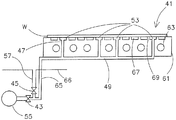
도 6은 본 발명의 또 다른 실시예에 따른 정전기 클램프의 평면도이다. 정정기 클램프(41)에는, 대상물 예컨대 기판(도 1에서 W)과 지지체 예컨대 기판 테이블(도 1에서 WT) 사이에 백필 가스(backfill gas)를 공급하는 백필 가스 시스템이 제공된다. 상기 백필 가스는 진공 환경에서 기판이 클램핑되고 기판 테이블(WT)의 일부분인 수온 제어 안정화 유닛(water controlled temperature stabilizing unit: 61) 사이의 열 전도도를 개선하는 데 사용된다. 진공에서의 열 전도도는 매우 낮으며, 이에 따라 기판의 온도가 점차 상승하여, 기판의 열 팽창을 유발하며 기판들의 노광 시 오버레이 난제들을 유발할 수 있는 위험이 존재한다. 백필 가스는 백필 가스 밸브(43)를 통해 연결된 백필 공급 시스템(55)으로부터 온도 안정화 유닛(61) 저부의 공급 채널(49)로 공급된다. 백필 가스는 12 개의 공급 구멍들(47)을 통해 원 형상을 갖는 2 개의 홈들(53)(여기서는 외측 원형 홈만이 원형 홈의 일부분을 나타내는 것으로 도시되어 있지만, 실제로 홈들(53)은 완전한 원형임)에 들어가며, 이는 백필 가스가 기판과 온도 안정화 유닛 사이의 공간을 채우게 한다. 기판(W)이 교체될 필요가 있는 경우, 백필 가스 밸브(43)가 폐쇄되고, 공급 채널(49)과 진공 공급 라인(57)을 연결하는 진공 밸브(45)가 개방될 것이므로, 기판(W)과 온도 제어 유닛 사이의 공간은 공급 구멍들(47) 및 홈들(53)을 통해 진공으로 흡입될 것이다. 기판과 온도 제어 유닛 사이가 진공 챔버 내의 진공과 유사한 진공에 도달된다면, 기판이 해제될 수 있다. 기판(W)이 교환되었으면, 진공 밸브(45)가 폐쇄될 것이며, 기판과 온도 제어 유닛 사이의 공간에 백필 가스를 공급하도록 백필 가스 밸브(43)가 개방될 것이다. 백필 가스가 스위치 오프(switch off)되고 진공이 인가되거나 또는 그 반대인 경우, 앞서 언급된 백필 공급 시스템은 빠른 응답 시간을 보장한다.6 is a plan view of an electrostatic clamp according to another embodiment of the present invention. The
도 7은 진공 벽(66)을 갖는 진공 챔버에 위치된 도 6의 정전기 클램프의 단면도이다(상기 벽은 부분적으로만 도시되며, 상기 벽은 정전기 클램프를 완전히 둘러싼다는 것을 이해하여야 한다). 백필 가스는 백필 가스 밸브(43), 공급 라인(65), 공급 채널(49), 공급 구멍(47) 및 홈들(53)을 통해, 기판(W)과 온도 안정화 유닛(61) 사이의 공간(67)으로 공급된다. 온도 안정화 유닛으로부터 소정 거리에서 기판(W)을 유지하기 위해, 상기 온도 안정화 유닛(61)에 돌출부들(69)이 제공된다. 상기 온도 안정화 유닛(61)에는 제어된 온도로 상기 온도 안정화 유닛(61)에 물을 제공하는 수로관들(63)이 제공된다. 또한, 정전기 클램프에는 진공 밸브(45)를 통해 공급 라인(65)으로 진공 챔버를 연결시키는 진공 공급 라인(57)이 제공된다. 백필 가스 시스템에 짧은 응답 시간을 제공하기 위해, 홈들(53)은 1 ㎟의 유동 표면을 가질 수 있고, 공급 구멍들(47)은 1.5mm의 직경을 갖는 원일 수 있으며, 공급 채널들(49)은 9 ㎟의 유동 표면을 가질 수 있고, 공급 라인(65)은 6mm의 직경을 갖는 원일 수 있다. 상기 채널들(49) 및 공급 라인들(57 및 65)은 빠른 응답 시간을 보장하기 위해 짧게, 예를 들어 50 cm보다 짧게 유지되는 것이 유익하다. 도 6 및 도 7의 정전기 클램프는 본 발명에 따라 버얼들이 제공된 지지체 및 상기 버얼들 사이에 제공된 절연체에 의해 둘러싸인 전극을 포함하며, 상기 지지체는 낮은 팽창 물질로 만들어질 수 있다. 대안적으로, 도 6 및 도 7의 정전기 클램프는 종래의 클램프 생성 기술들에 의해 만들어질 수 있다.Fig. 7 is a cross-sectional view of the electrostatic clamp of Fig. 6 located in a vacuum chamber with a vacuum wall 66 (it should be understood that the wall is only partially shown, and that the wall completely surrounds the electrostatic clamp). The backfill gas is supplied to the space between the substrate W and the
또 다른 실시예에 따르면, 정전기 클램프에는 전극 제어부(85)에 연결된 내측 전극(83) 및 외측 전극(81)(도 8 참조)이 제공될 수 있다. 기판(W)이 교체될 필요가 있는 경우, 외측 전극(81)은 상기 제어부(85)에 의해 비활성화(deactivate)될 것이고, 따라서 대상물(기판)이 약간 휠 것이며, 기판과 외측 전극(81) 사이에서 상기 기판과 클램프를 둘러싸는 진공 공간으로 백필 가스가 배출될 수 있다. 기판과 온도 제어 유닛 사이의 공간이 진공 압력에 있는 경우, 내측 전극이 비활성화될 것이며, 기판이 완전히 해제될 수 있다. 기판과 클램프 사이의 공간이 진공에 이르는 응답 시간은 외측 및 내측 전극을 이용하는 상기 방법에 의해 단축될 수 있다. 도 8의 전극은 본 발명에 따라 버얼들이 제공된 지지체 및 상기 버얼들 사이에 제공된 절연체에 의해 둘러싸인 전극을 포함하며, 상기 지지체는 낮은 팽창 물질로 만들어질 수 있다. 대안적으로, 도 8의 정전기 클램프는 종래의 기술들에 의해 만들어질 수 있다.According to another embodiment, the electrostatic clamp may be provided with an
본 명세서에서는, IC 제조에 있어서 리소그래피 장치의 특정 사용예에 대하여 언급되지만, 본 명세서에 서술된 리소그래피 장치는 집적 광학 시스템, 자기 도메인 메모리용 안내 및 검출 패턴, 평판 디스플레이(flat-panel display), 액정 디스플레이(LCD), 박막 자기 헤드 등의 제조와 같이 다른 적용예들을 가질 수도 있음을 이해하여야 한다. 당업자라면, 이러한 대안적인 적용예와 관련하여, 본 명세서의 "웨이퍼" 또는 "다이"라는 용어의 어떠한 사용도 각각 "기판" 또는 "타겟부"라는 좀 더 일반적인 용어와 동의어로 간주될 수도 있음을 이해할 것이다. 본 명세서에서 언급되는 기판은 노광 전후에, 예를 들어 트랙(전형적으로, 기판에 레지스트 층을 도포하고 노광된 레지스트를 현상하는 툴), 메트롤로지 툴 및/또는 검사 툴에서 처리될 수 있다. 적용가능하다면, 이러한 기판 처리 툴과 다른 기판 처리 툴에 본 명세서의 기재 내용이 적용될 수 있다. 또한, 예를 들어 다층 IC를 생성하기 위하여 기판이 한번 이상 처리될 수 있으므로, 본 명세서에 사용되는 기판이라는 용어는 이미 여러번 처리된 층들을 포함한 기판을 칭할 수도 있다.Although specific reference may be made in this text to the use of lithographic apparatus in the manufacture of ICs, the lithographic apparatus described herein may have other applications, such as the manufacture of integrated optical systems, guidance and detection patterns for magnetic domain memories, flat-panel displays, Display (LCD), thin-film magnetic heads, and the like. Those skilled in the art will recognize that any use of the terms "wafer" or "die" herein may be considered as synonymous with the more general terms "substrate" or "target portion", respectively, in connection with this alternative application I will understand. The substrate referred to herein can be processed before and after exposure, for example in a track (typically a tool that applies a resist layer to a substrate and develops the exposed resist), a metrology tool, and / or an inspection tool. Where applicable, the description herein may be applied to such substrate processing tools and other substrate processing tools. Further, the substrate may be processed more than once, for example in order to create a multi-layer IC, so that the term substrate used herein may also refer to a substrate that already contains multiple processed layers.
이상, 광학 리소그래피와 관련하여 본 발명의 실시예들의 특정 사용예를 언급하였지만, 본 발명은 다른 적용예들, 예를 들어 임프린트 리소그래피에 사용될 수 있으며, 본 명세서가 허용한다면 광학 리소그래피로 제한되지 않는다는 것을 이해할 것이다. 임프린트 리소그래피에서, 패터닝 디바이스 내의 토포그래피(topography)는 기판 상에 생성된 패턴을 정의한다. 패터닝 디바이스의 토포그래피는 전자기 방사선, 열, 압력 또는 그 조합을 인가함으로써 레지스트가 경화되는 기판에 공급된 레지스트 층으로 가압될 수 있다. 패터닝 디바이스는 레지스트를 벗어나 이동하며, 레지스트가 경화된 후에 그 안에 패턴을 남긴다.While specific reference may have been made above to the use of embodiments of the invention in connection with optical lithography, it is to be understood that the invention may be used in other applications, for example imprint lithography, and is not limited to optical lithography, I will understand. In imprint lithography, topography in a patterning device defines a pattern created on a substrate. The topography of the patterning device can be pressed into the resist layer supplied to the substrate on which the resist is cured by applying electromagnetic radiation, heat, pressure, or a combination thereof. The patterning device moves out of the resist and leaves a pattern therein after the resist is cured.
본 명세서에서 사용된 "방사선" 및 "빔"이라는 용어는 (예를 들어, 365, 355, 248, 193, 157 또는 126 nm, 또는 그 정도의 파장을 갖는) 자외(UV) 방사선 및 (예를 들어, 5 내지 20 nm 범위 내의 파장을 갖는) 극자외(EUV) 방사선뿐만 아니라, 이온 빔 또는 전자 빔과 같은 입자 빔을 포함하는 모든 형태의 전자기 방사선을 포괄한다.The terms "radiation" and "beam" used herein encompass all types of electromagnetic radiation, including ultraviolet (UV) radiation (e.g. having a wavelength of, for example, 365, 355, 248, 193, 157 or 126 nm, Extreme ultra-violet (EUV) radiation (having a wavelength in the range of 5-20 nm), as well as particle beams, such as ion beams or electron beams.
본 명세서가 허용하는 "렌즈"라는 용어는, 굴절, 반사, 자기, 전자기 및 정전기 광학 구성요소들을 포함하는 다양한 형태의 광학 구성요소들 중 어느 하나 또는 그 조합으로 언급될 수 있다.The term "lens ", as the context allows, may refer to any one or combination of various types of optical components, including refractive, reflective, magnetic, electromagnetic and electrostatic optical components.
상기 서술내용은 예시를 위한 것이지, 제한하려는 것이 아니다. 따라서, 당업자라면 아래에 설명되는 청구항들의 범위를 벗어나지 않고 서술된 본 발명에 대한 변형예가 행해질 수도 있음을 이해할 것이다.The above description is intended to be illustrative, not limiting. Accordingly, those skilled in the art will appreciate that modifications may be made to the invention as described without departing from the scope of the claims set forth below.
Claims (20)
상기 클램프는 버얼들이 제공된 지지체를 포함하고, 상기 버얼들의 최상부는 상기 대상물이 유지되는 상기 평면을 결정하며, 절연체에 의해 둘러싸인 전극이 상기 버얼들 사이에 제공되고, 상기 지지체는 10 m/m.K x 10-6 미만의 팽창 계수를 갖는 물질로 만들어지며,
상기 버얼들은 상기 지지체와 동일한 물질로 만들어지는 정전기 클램프.An electrostatic clamp for holding an object in a fixed plane within a lithographic apparatus in use,
Wherein the clamp comprises a support provided with burls, the top of the burls defining the plane in which the object is held, an electrode surrounded by an insulator is provided between the burls, and the support has a length of 10 m / Is made of a material having an expansion coefficient of less than -6 ,
Wherein the burls are made of the same material as the support.
상기 전극은, 상기 버얼들의 최상부(top portions)보다 높게 연장되지 않고 상기 버얼들의 최하부(bottom)보다 낮게 연장되지 않도록 구성되는 정전기 클램프.The method according to claim 1,
Wherein the electrode is configured not to extend above the top portions of the burls but to extend below the bottoms of the burls.
상기 지지체는 4 m/m.K x 10-6 미만의 팽창 계수를 갖는 물질로 만들어지는 정전기 클램프.The method according to claim 1,
Wherein said support is made of a material having an expansion coefficient of less than 4 m / mK x 10 <" 6 & gt ;.
상기 클램프는 버얼들이 제공된 지지체를 포함하고, 상기 버얼들의 최상부는 상기 대상물이 유지되는 상기 평면을 결정하며, 절연체에 의해 둘러싸인 전극이 상기 버얼들 사이에 제공되고, 상기 지지체는 10 m/m.K x 10-6 미만의 팽창 계수를 갖는 물질로 만들어지며,
상기 지지체와 상기 버얼들은 하나의 구성부(one piece)로 만들어지는 정전기 클램프.An electrostatic clamp for holding an object in a fixed plane within a lithographic apparatus in use,
Wherein the clamp comprises a support provided with burls, the top of the burls defining the plane in which the object is held, an electrode surrounded by an insulator is provided between the burls, and the support has a length of 10 m / Is made of a material having an expansion coefficient of less than -6 ,
Wherein the support and the burls are made of one piece.
상기 정전기 클램프에는 온도 제어 시스템이 제공되는 정전기 클램프.5. The method according to any one of claims 1 to 4,
Wherein the electrostatic clamp is provided with a temperature control system.
상기 온도 제어 시스템은 수로관(water duct)을 포함하는 정전기 클램프.6. The method of claim 5,
Wherein the temperature control system includes a water duct.
상기 버얼이 제공된 상기 지지체는 비금속으로 만들어지는 정전기 클램프.5. The method according to any one of claims 1 to 4,
Wherein the support provided with the burr is made of a non-metallic material.
상기 절연체는 유전 물질이고, 상기 유전 물질은 Parylene®, Kapton®, Mylar®, 석영, 액정 중합체(liquid crytal polymer), 또는 보륨 질화물(borium nitride)인 정전기 클램프.5. The method according to any one of claims 1 to 4,
Wherein the insulator is a dielectric material and the dielectric material is Parylene®, Kapton®, Mylar®, quartz, liquid crytal polymer, or borium nitride.
상기 정전기 클램프에는 상기 대상물과 상기 지지체 사이에 백필 가스(backfill gas)를 공급하는 백필 가스 시스템이 제공되는 정전기 클램프.5. The method according to any one of claims 1 to 4,
Wherein the electrostatic clamp is provided with a backfill gas system for supplying backfill gas between the object and the support.
상기 클램프는 버얼들이 제공된 지지체를 포함하고, 상기 버얼들의 최상부는 상기 대상물이 유지되는 상기 평면을 결정하며, 절연체에 의해 둘러싸인 전극이 상기 버얼들 사이에 제공되고, 상기 지지체는 10 m/m.K x 10-6 미만의 팽창 계수를 갖는 물질로 만들어지며,
상기 클램프에는 전극 제어부에 연결된 내측 및 외측 전극이 제공되며, 상기 전극 제어부는 상기 대상물의 해제 이전에 백필 가스가 배출될 수 있도록, 상기 대상물의 해제 동안에 내측 전극에 앞서 외측 전극을 비활성화하도록 구성되고 배치되는 정전기 클램프.An electrostatic clamp for holding an object in a fixed plane within a lithographic apparatus in use,
Wherein the clamp comprises a support provided with burls, the top of the burls defining the plane in which the object is held, an electrode surrounded by an insulator is provided between the burls, and the support has a length of 10 m / Is made of a material having an expansion coefficient of less than -6 ,
Wherein the clamp is provided with inner and outer electrodes connected to an electrode control and wherein the electrode control is configured to deactivate the outer electrode prior to the inner electrode during release of the object so that backfill gas can be discharged prior to release of the object, Electrostatic Clamps.
버얼들을 갖는 물질 층을 제공하는 단계, 및
상기 버얼들 사이에 절연체 및/또는 유전 물질에 의해 둘러싸인 전극을 배치시키는 단계를 포함하고,
상기 버얼들은 상기 대상물 지지체와 동일한 물질로 만들어지는 정전기 클램프를 제조하는 방법.A method of fabricating an electrostatic clamp configured to electrostatically clamp an object against an object support in a lithographic apparatus,
Providing a layer of material having burls, and
Placing an electrode surrounded by an insulator and / or a dielectric material between the burls,
Wherein the burls are made of the same material as the object support.
상기 제조 방법은 상기 절연체 및/또는 유전 물질을 제공하기 위해 스퍼터링 공정, 화학 기상 증착 공정 또는 이들의 조합을 이용하는 단계를 포함하는 정전기 클램프를 제조하는 방법.12. The method of claim 11,
Wherein the method comprises using a sputtering process, a chemical vapor deposition process, or a combination thereof to provide the insulator and / or dielectric material.
상기 절연체는 서로 다른 두 개의 재료를 포함하는 정전기 클램프.5. The method according to any one of claims 1 to 4,
Wherein the insulator comprises two different materials.
방사선 빔의 빔 경로 내의 대상물을 지지하도록 구성된 대상물 지지체; 및
상기 대상물을 상기 대상물 지지체에 클램핑하도록 구성된 제 1 항 내지 제 4 항 및 제 10 항 중 어느 한 항을 따른 정전기 클램프를 포함하는 리소그래피 장치.
In a lithographic apparatus,
An object support configured to support an object in a beam path of the radiation beam; And
A lithographic apparatus comprising an electrostatic clamp according to any one of claims 1 to 4 and 10, configured to clamp the object to the object support.
Applications Claiming Priority (3)
| Application Number | Priority Date | Filing Date | Title |
|---|---|---|---|
| US11/902,501 | 2007-09-21 | ||
| US11/902,501 US7940511B2 (en) | 2007-09-21 | 2007-09-21 | Electrostatic clamp, lithographic apparatus and method of manufacturing an electrostatic clamp |
| PCT/EP2008/007916 WO2009036995A1 (en) | 2007-09-21 | 2008-09-19 | Electrostatic clamp, lithographic apparatus and method of manufacturing an electrostatic clamp |
Publications (2)
| Publication Number | Publication Date |
|---|---|
| KR20100075517A KR20100075517A (en) | 2010-07-02 |
| KR101533014B1 true KR101533014B1 (en) | 2015-07-01 |
Family
ID=39929545
Family Applications (1)
| Application Number | Title | Priority Date | Filing Date |
|---|---|---|---|
| KR1020107008658A KR101533014B1 (en) | 2007-09-21 | 2008-09-19 | Electrostatic clamp, lithographic apparatus and method of manufacturing an electrostatic clamp |
Country Status (8)
| Country | Link |
|---|---|
| US (2) | US7940511B2 (en) |
| EP (1) | EP2208224B1 (en) |
| JP (1) | JP5524845B2 (en) |
| KR (1) | KR101533014B1 (en) |
| CN (1) | CN101803001B (en) |
| NL (1) | NL1035888A1 (en) |
| TW (1) | TWI446482B (en) |
| WO (1) | WO2009036995A1 (en) |
Families Citing this family (33)
| Publication number | Priority date | Publication date | Assignee | Title |
|---|---|---|---|---|
| US7940511B2 (en) * | 2007-09-21 | 2011-05-10 | Asml Netherlands B.V. | Electrostatic clamp, lithographic apparatus and method of manufacturing an electrostatic clamp |
| JP2010161319A (en) * | 2009-01-09 | 2010-07-22 | Nikon Corp | Electrostatic chucking device, exposure apparatus, and device manufacturing method |
| EP2365390A3 (en) * | 2010-03-12 | 2017-10-04 | ASML Netherlands B.V. | Lithographic apparatus and method |
| WO2012005294A1 (en) * | 2010-07-09 | 2012-01-12 | 株式会社クリエイティブ テクノロジー | Electrostatic chuck device and production method for same |
| WO2012076207A1 (en) * | 2010-12-08 | 2012-06-14 | Asml Holding N.V. | Electrostatic clamp, lithographic apparatus and method of manufacturing an electrostatic clamp |
| NL2007768A (en) | 2010-12-14 | 2012-06-18 | Asml Netherlands Bv | Substrate holder, lithographic apparatus, device manufacturing method, and method of manufacturing a substrate holder. |
| EP2490073B1 (en) | 2011-02-18 | 2015-09-23 | ASML Netherlands BV | Substrate holder, lithographic apparatus, and method of manufacturing a substrate holder |
| US9366973B2 (en) * | 2011-02-18 | 2016-06-14 | Asml Netherlands B.V. | Lithographic apparatus and device manufacturing method |
| US9360771B2 (en) * | 2011-03-17 | 2016-06-07 | Asml Netherlands B.V. | Electrostatic clamp, lithographic apparatus, and device manufacturing method |
| NL2008630A (en) | 2011-04-27 | 2012-10-30 | Asml Netherlands Bv | Substrate holder, lithographic apparatus, device manufacturing method, and method of manufacturing a substrate holder. |
| NL2009487A (en) | 2011-10-14 | 2013-04-16 | Asml Netherlands Bv | Substrate holder, lithographic apparatus, device manufacturing method, and method of manufacturing a substrate holder. |
| KR101652782B1 (en) | 2012-02-03 | 2016-08-31 | 에이에스엠엘 네델란즈 비.브이. | Substrate holder and lithographic apparatus |
| WO2013127589A1 (en) | 2012-02-29 | 2013-09-06 | Asml Netherlands B.V. | Electrostatic clamp |
| US9449865B2 (en) | 2012-07-17 | 2016-09-20 | Asml Netherlands B.V. | Electrostatic clamp, lithographic apparatus and method |
| US9104113B2 (en) | 2013-01-07 | 2015-08-11 | International Business Machines Corporation | Amplification method for photoresist exposure in semiconductor chip manufacturing |
| US9541846B2 (en) | 2013-09-06 | 2017-01-10 | Taiwan Semiconductor Manufacturing Co., Ltd. | Homogeneous thermal equalization with active device |
| US9101038B2 (en) | 2013-12-20 | 2015-08-04 | Lam Research Corporation | Electrostatic chuck including declamping electrode and method of declamping |
| DE102014008031B4 (en) * | 2014-05-28 | 2020-06-25 | Berliner Glas Kgaa Herbert Kubatz Gmbh & Co. | Electrostatic holding device with a ceramic electrode and method for producing such a holding device |
| TWI656596B (en) | 2014-08-26 | 2019-04-11 | 荷蘭商Asml控股公司 | Electrostatic clamp and manufacturing method thereof |
| US10002782B2 (en) | 2014-10-17 | 2018-06-19 | Lam Research Corporation | ESC assembly including an electrically conductive gasket for uniform RF power delivery therethrough |
| WO2016135565A1 (en) * | 2015-02-23 | 2016-09-01 | M Cubed Technologies, Inc. | Film electrode for electrostatic chuck |
| JP6650345B2 (en) * | 2016-05-26 | 2020-02-19 | 日本特殊陶業株式会社 | Substrate holding device and method of manufacturing the same |
| CN110720138A (en) * | 2017-06-22 | 2020-01-21 | 应用材料公司 | Electrostatic carrier for die bonding applications |
| DE102018116463A1 (en) | 2018-07-06 | 2020-01-09 | Berliner Glas Kgaa Herbert Kubatz Gmbh & Co. | Electrostatic chuck and method of making the same |
| NL2024752A (en) * | 2019-02-08 | 2020-08-19 | Asml Netherlands Bv | Component for use in a Lithographic Apparatus, Method of Manufacturing a Component and Method of Protecting Tables in a Lithographic Apparatus |
| DE102019108855B4 (en) * | 2019-04-04 | 2020-11-12 | Berliner Glas Kgaa Herbert Kubatz Gmbh & Co. | Electrostatic holding device with a layer composite electrode device and method for its production |
| WO2020239373A1 (en) | 2019-05-24 | 2020-12-03 | Asml Holding N.V. | Lithographic apparatus, substrate table, and method |
| US11817293B2 (en) * | 2020-01-10 | 2023-11-14 | The Research Foundation For The State University Of New York | Photoresist layers of semiconductor components including electric fields, system, and methods of forming same |
| US11875967B2 (en) | 2020-05-21 | 2024-01-16 | Applied Materials, Inc. | System apparatus and method for enhancing electrical clamping of substrates using photo-illumination |
| US11538714B2 (en) * | 2020-05-21 | 2022-12-27 | Applied Materials, Inc. | System apparatus and method for enhancing electrical clamping of substrates using photo-illumination |
| EP3923077A1 (en) * | 2020-06-11 | 2021-12-15 | ASML Netherlands B.V. | Object holder, electrostatic sheet and method for making an electrostatic sheet |
| EP4053634A1 (en) * | 2021-03-02 | 2022-09-07 | ASML Netherlands B.V. | Substrate restraining system |
| EP4105720A1 (en) * | 2021-06-16 | 2022-12-21 | ASML Netherlands B.V. | Substrate holder and method |
Citations (2)
| Publication number | Priority date | Publication date | Assignee | Title |
|---|---|---|---|---|
| JP2004196589A (en) * | 2002-12-18 | 2004-07-15 | Ngk Spark Plug Co Ltd | Ceramic sintered compact and its producing method |
| JP2007221101A (en) * | 2005-12-21 | 2007-08-30 | Asml Netherlands Bv | Method for manufacturing lithography system and electrostatic clamp for lithography system |
Family Cites Families (22)
| Publication number | Priority date | Publication date | Assignee | Title |
|---|---|---|---|---|
| GB2106325A (en) * | 1981-09-14 | 1983-04-07 | Philips Electronic Associated | Electrostatic chuck |
| US5880924A (en) * | 1997-12-01 | 1999-03-09 | Applied Materials, Inc. | Electrostatic chuck capable of rapidly dechucking a substrate |
| US6067222A (en) * | 1998-11-25 | 2000-05-23 | Applied Materials, Inc. | Substrate support apparatus and method for fabricating same |
| JP2000340640A (en) * | 1999-05-31 | 2000-12-08 | Toto Ltd | Non-contacting electrostatically attracting apparatus |
| US6426790B1 (en) * | 2000-02-28 | 2002-07-30 | Nikon Corporation | Stage apparatus and holder, and scanning exposure apparatus and exposure apparatus |
| JP4467836B2 (en) * | 2001-06-08 | 2010-05-26 | 株式会社アルバック | Deposition method |
| DE10157487C1 (en) * | 2001-11-23 | 2003-06-18 | Sgl Carbon Ag | Fiber-reinforced composite body for protective armor, its manufacture and uses |
| US20030233977A1 (en) * | 2002-06-20 | 2003-12-25 | Yeshwanth Narendar | Method for forming semiconductor processing components |
| JP2004031594A (en) * | 2002-06-25 | 2004-01-29 | Kyocera Corp | Electrostatic chuck and its manufacturing method |
| US7092231B2 (en) * | 2002-08-23 | 2006-08-15 | Asml Netherlands B.V. | Chuck, lithographic apparatus and device manufacturing method |
| JP4101017B2 (en) * | 2002-10-24 | 2008-06-11 | 株式会社アルバック | Adsorption device and adsorption method |
| JP4472372B2 (en) * | 2003-02-03 | 2010-06-02 | 株式会社オクテック | Plasma processing apparatus and electrode plate for plasma processing apparatus |
| KR100512745B1 (en) * | 2003-07-24 | 2005-09-07 | 삼성전자주식회사 | Elecrostatic Chuck |
| JP2005150370A (en) * | 2003-11-14 | 2005-06-09 | Kyocera Corp | Electrostatic chuck |
| JP2005268720A (en) * | 2004-03-22 | 2005-09-29 | Disco Abrasive Syst Ltd | Etching apparatus |
| US7133120B2 (en) * | 2004-05-04 | 2006-11-07 | Asml Netherlands B.V. | Lithographic apparatus, article support member, and method |
| US20070097346A1 (en) * | 2005-10-28 | 2007-05-03 | Asml Netherlands B.V. | Lithographic apparatus and device manufacturing method |
| US7564536B2 (en) * | 2005-11-08 | 2009-07-21 | Asml Netherlands B.V. | Lithographic apparatus and device manufacturing method |
| US7646581B2 (en) * | 2006-01-31 | 2010-01-12 | Sumitomo Osaka Cement Co., Ltd. | Electrostatic chuck |
| US8325321B2 (en) * | 2006-07-28 | 2012-12-04 | Mapper Lithography Ip B.V. | Lithography system, method of heat dissipation and frame |
| US7940511B2 (en) * | 2007-09-21 | 2011-05-10 | Asml Netherlands B.V. | Electrostatic clamp, lithographic apparatus and method of manufacturing an electrostatic clamp |
| JP4974873B2 (en) * | 2007-12-26 | 2012-07-11 | 新光電気工業株式会社 | Electrostatic chuck and substrate temperature control fixing device |
-
2007
- 2007-09-21 US US11/902,501 patent/US7940511B2/en active Active
-
2008
- 2008-09-02 NL NL1035888A patent/NL1035888A1/en active Search and Examination
- 2008-09-19 KR KR1020107008658A patent/KR101533014B1/en active IP Right Grant
- 2008-09-19 WO PCT/EP2008/007916 patent/WO2009036995A1/en active Application Filing
- 2008-09-19 EP EP08802422.9A patent/EP2208224B1/en active Active
- 2008-09-19 CN CN200880107793XA patent/CN101803001B/en active Active
- 2008-09-19 JP JP2010525264A patent/JP5524845B2/en active Active
- 2008-09-19 TW TW097136226A patent/TWI446482B/en active
-
2011
- 2011-03-22 US US13/069,203 patent/US8098475B2/en active Active
Patent Citations (2)
| Publication number | Priority date | Publication date | Assignee | Title |
|---|---|---|---|---|
| JP2004196589A (en) * | 2002-12-18 | 2004-07-15 | Ngk Spark Plug Co Ltd | Ceramic sintered compact and its producing method |
| JP2007221101A (en) * | 2005-12-21 | 2007-08-30 | Asml Netherlands Bv | Method for manufacturing lithography system and electrostatic clamp for lithography system |
Also Published As
| Publication number | Publication date |
|---|---|
| EP2208224B1 (en) | 2019-11-06 |
| TW200929429A (en) | 2009-07-01 |
| CN101803001A (en) | 2010-08-11 |
| EP2208224A1 (en) | 2010-07-21 |
| NL1035888A1 (en) | 2009-03-24 |
| US20110170085A1 (en) | 2011-07-14 |
| CN101803001B (en) | 2012-11-07 |
| US20090079525A1 (en) | 2009-03-26 |
| US8098475B2 (en) | 2012-01-17 |
| WO2009036995A1 (en) | 2009-03-26 |
| TWI446482B (en) | 2014-07-21 |
| JP2010541196A (en) | 2010-12-24 |
| US7940511B2 (en) | 2011-05-10 |
| JP5524845B2 (en) | 2014-06-18 |
| KR20100075517A (en) | 2010-07-02 |
Similar Documents
| Publication | Publication Date | Title |
|---|---|---|
| KR101533014B1 (en) | Electrostatic clamp, lithographic apparatus and method of manufacturing an electrostatic clamp | |
| TWI621927B (en) | A substrate holder, a lithographic apparatus and method of manufacturing devices | |
| JP5960154B2 (en) | Electrostatic clamp, lithographic apparatus, and method of manufacturing electrostatic clamp | |
| KR100705497B1 (en) | Apparatus, method for supporting and/or thermally conditioning a substrate, a support table, and a chuck | |
| KR100883610B1 (en) | Lithographic apparatus and method of manufacturing an electrostatic clamp for a lithographic apparatus | |
| KR100801951B1 (en) | Lithographic apparatus and device manufacturing method | |
| TWI582540B (en) | Electrostatic clamp, lithographic apparatus and method of manufacturing an electrostatic clamp | |
| KR100801952B1 (en) | Lithographic Apparatus and Device Manufacturing Method | |
| KR20150109448A (en) | Electrostatic clamp | |
| KR20120072336A (en) | Lithographic apparatus and removable member | |
| US7327439B2 (en) | Lithographic apparatus and device manufacturing method | |
| TWI470362B (en) | Lithographic apparatus and method | |
| KR20220154695A (en) | Object holders, tools and methods of manufacturing object holders | |
| TW202243107A (en) | Clamp electrode modification for improved overlay |
Legal Events
| Date | Code | Title | Description |
|---|---|---|---|
| A201 | Request for examination | ||
| E902 | Notification of reason for refusal | ||
| E902 | Notification of reason for refusal | ||
| E701 | Decision to grant or registration of patent right | ||
| GRNT | Written decision to grant | ||
| FPAY | Annual fee payment |
Payment date: 20180619 Year of fee payment: 4 |