KR101492520B1 - Optical storage medium comprising tracks with positive and negative marks, and stampers and production methods for manufacturing of the optical storage medium - Google Patents
Optical storage medium comprising tracks with positive and negative marks, and stampers and production methods for manufacturing of the optical storage medium Download PDFInfo
- Publication number
- KR101492520B1 KR101492520B1 KR20097006433A KR20097006433A KR101492520B1 KR 101492520 B1 KR101492520 B1 KR 101492520B1 KR 20097006433 A KR20097006433 A KR 20097006433A KR 20097006433 A KR20097006433 A KR 20097006433A KR 101492520 B1 KR101492520 B1 KR 101492520B1
- Authority
- KR
- South Korea
- Prior art keywords
- positive
- negative
- mark
- photoresist
- plate
- Prior art date
Links
Images


Classifications
-
- G—PHYSICS
- G11—INFORMATION STORAGE
- G11B—INFORMATION STORAGE BASED ON RELATIVE MOVEMENT BETWEEN RECORD CARRIER AND TRANSDUCER
- G11B7/00—Recording or reproducing by optical means, e.g. recording using a thermal beam of optical radiation by modifying optical properties or the physical structure, reproducing using an optical beam at lower power by sensing optical properties; Record carriers therefor
- G11B7/24—Record carriers characterised by shape, structure or physical properties, or by the selection of the material
- G11B7/2407—Tracks or pits; Shape, structure or physical properties thereof
- G11B7/24073—Tracks
-
- G—PHYSICS
- G11—INFORMATION STORAGE
- G11B—INFORMATION STORAGE BASED ON RELATIVE MOVEMENT BETWEEN RECORD CARRIER AND TRANSDUCER
- G11B7/00—Recording or reproducing by optical means, e.g. recording using a thermal beam of optical radiation by modifying optical properties or the physical structure, reproducing using an optical beam at lower power by sensing optical properties; Record carriers therefor
- G11B7/24—Record carriers characterised by shape, structure or physical properties, or by the selection of the material
- G11B7/26—Apparatus or processes specially adapted for the manufacture of record carriers
- G11B7/261—Preparing a master, e.g. exposing photoresist, electroforming
-
- B—PERFORMING OPERATIONS; TRANSPORTING
- B29—WORKING OF PLASTICS; WORKING OF SUBSTANCES IN A PLASTIC STATE IN GENERAL
- B29D—PRODUCING PARTICULAR ARTICLES FROM PLASTICS OR FROM SUBSTANCES IN A PLASTIC STATE
- B29D17/00—Producing carriers of records containing fine grooves or impressions, e.g. disc records for needle playback, cylinder records; Producing record discs from master stencils
-
- G—PHYSICS
- G11—INFORMATION STORAGE
- G11B—INFORMATION STORAGE BASED ON RELATIVE MOVEMENT BETWEEN RECORD CARRIER AND TRANSDUCER
- G11B7/00—Recording or reproducing by optical means, e.g. recording using a thermal beam of optical radiation by modifying optical properties or the physical structure, reproducing using an optical beam at lower power by sensing optical properties; Record carriers therefor
- G11B7/007—Arrangement of the information on the record carrier, e.g. form of tracks, actual track shape, e.g. wobbled, or cross-section, e.g. v-shaped; Sequential information structures, e.g. sectoring or header formats within a track
- G11B7/013—Arrangement of the information on the record carrier, e.g. form of tracks, actual track shape, e.g. wobbled, or cross-section, e.g. v-shaped; Sequential information structures, e.g. sectoring or header formats within a track for discrete information, i.e. where each information unit is stored in a distinct discrete location, e.g. digital information formats within a data block or sector
-
- G—PHYSICS
- G11—INFORMATION STORAGE
- G11B—INFORMATION STORAGE BASED ON RELATIVE MOVEMENT BETWEEN RECORD CARRIER AND TRANSDUCER
- G11B7/00—Recording or reproducing by optical means, e.g. recording using a thermal beam of optical radiation by modifying optical properties or the physical structure, reproducing using an optical beam at lower power by sensing optical properties; Record carriers therefor
- G11B7/24—Record carriers characterised by shape, structure or physical properties, or by the selection of the material
- G11B7/2407—Tracks or pits; Shape, structure or physical properties thereof
- G11B7/24085—Pits
-
- G—PHYSICS
- G11—INFORMATION STORAGE
- G11B—INFORMATION STORAGE BASED ON RELATIVE MOVEMENT BETWEEN RECORD CARRIER AND TRANSDUCER
- G11B7/00—Recording or reproducing by optical means, e.g. recording using a thermal beam of optical radiation by modifying optical properties or the physical structure, reproducing using an optical beam at lower power by sensing optical properties; Record carriers therefor
- G11B7/24—Record carriers characterised by shape, structure or physical properties, or by the selection of the material
- G11B7/26—Apparatus or processes specially adapted for the manufacture of record carriers
-
- G—PHYSICS
- G11—INFORMATION STORAGE
- G11B—INFORMATION STORAGE BASED ON RELATIVE MOVEMENT BETWEEN RECORD CARRIER AND TRANSDUCER
- G11B7/00—Recording or reproducing by optical means, e.g. recording using a thermal beam of optical radiation by modifying optical properties or the physical structure, reproducing using an optical beam at lower power by sensing optical properties; Record carriers therefor
- G11B7/24—Record carriers characterised by shape, structure or physical properties, or by the selection of the material
- G11B7/2407—Tracks or pits; Shape, structure or physical properties thereof
- G11B7/24073—Tracks
- G11B7/24079—Width or depth
-
- G—PHYSICS
- G11—INFORMATION STORAGE
- G11B—INFORMATION STORAGE BASED ON RELATIVE MOVEMENT BETWEEN RECORD CARRIER AND TRANSDUCER
- G11B7/00—Recording or reproducing by optical means, e.g. recording using a thermal beam of optical radiation by modifying optical properties or the physical structure, reproducing using an optical beam at lower power by sensing optical properties; Record carriers therefor
- G11B7/24—Record carriers characterised by shape, structure or physical properties, or by the selection of the material
- G11B7/26—Apparatus or processes specially adapted for the manufacture of record carriers
- G11B7/263—Preparing and using a stamper, e.g. pressing or injection molding substrates
Landscapes
- Engineering & Computer Science (AREA)
- Manufacturing & Machinery (AREA)
- Mechanical Engineering (AREA)
- Manufacturing Optical Record Carriers (AREA)
- Optical Record Carriers And Manufacture Thereof (AREA)
Abstract
Description
본 발명은 기판층, 이 기판층 상의 트랙 내에 배열되는 마크 및 공간 구조를 갖는 판독 전용 데이터층과 덮개층을 포함하는 광 저장 매체, 및 이 광 저장 매체의 각 생산에 관한 것이다. 또한, 이 광 저장 매체는 특히 고 데이터 밀도로 데이터를 저장하기 위한 초 해상도 근접장 구조(super-resolution near-field structure)를 갖는 마스크층을 포함한다. The present invention relates to an optical storage medium comprising a substrate layer, a read only data layer having a mark and space structure arranged in the track on the substrate layer and a cover layer, and each production of the optical storage medium. The optical storage medium also includes a mask layer having a super-resolution near-field structure for storing data, especially at high data densities.
광 저장 매체는, 예를 들면 광 저장 매체를 조명하기 위한 레이저와 데이터를 판독하는 경우 레이저 빔의 반사된 광을 검출하기 위한 포토 검출기를 포함하는 픽업을 써서, 광학적으로 판독가능한 방식으로 데이터가 저장되는 매체이다. 한편으로, 널리 다양한 광 저장 매체가 이용가능한데, 이 저장 매체는 상이한 레이저 파장으로 동작되고, 1기가바이트 미만부터 50 기가바이트(GB)까지 저장 용량을 제공하기 위해 상이한 사이즈를 갖는다. 포맷은 재기록 가능한 포맷뿐만 아니라 1회 기록 광 매체인 오디오 CD 및 비디오 DVD와 같은 판독 전용 포맷(ROM)을 포함한다. 디지털 데이터는 매체의 하나 이상 층에 있는 트랙을 따라 이들 매체 상에 저장된다. The optical storage medium includes a laser for illuminating an optical storage medium and a pickup for detecting the reflected light of the laser beam when reading the data so that the data is stored in an optically readable manner . On the one hand, a wide variety of optical storage media are available, which operate at different laser wavelengths and have different sizes to provide storage capacities from less than 1 gigabyte to 50 gigabytes (GB). The format includes a rewritable format as well as a read-only format (ROM) such as an audio CD and a video DVD, which are write-once optical media. Digital data is stored on these media along tracks in more than one layer of media.
최고 데이터 용량을 갖는 저장 매체는 현재 블루 레이 디스크(BD)이며, 이 디스크는 듀얼층 디스크 상에 50GB의 저장을 허용한다. 이용가능한 포맷은 현재 예를 들면 판독 전용 BD-ROM, 재기록 가능한 BD-RE 및 일회 기록용 BD-R 디스크이다. 블루 레이 디스크의 판독 및 기록에 대하여, 405nm의 레이저 파장을 갖는 광 픽업이 사용된다. 블루 레이 디스크 상에서, 320nm의 트랙 피치 및 2T 내지 8T, 최대 9T까지의 마크 길이가 사용되며, 여기서 T는 69 - 80nm의 길이와 상응하는 채널 비트 길이이다. 블루 레이 디스크 시스템에 관한 추가 정보는 예를 들면 인터넷을 통해 블루 레이 그룹, 즉 www.blu-raydisc.com으로부터 입수할 수 있다. The storage medium with the highest data capacity is currently Blu-ray Disc (BD), which allows storage of 50 GB on dual layer discs. Available formats are, for example, a read-only BD-ROM, a rewritable BD-RE, and a BD-R disc for once recording. An optical pickup having a laser wavelength of 405 nm is used for reading and writing of a Blu-ray disc. On a Blu-ray disc, a track pitch of 320 nm and a mark length of 2T to 8T, up to 9T are used, where T is a length of 69-80 nm and a corresponding channel bit length. Additional information on Blu-ray disc systems is available, for example, from the Blu-ray group, www.blu-raydisc.com, via the Internet.
초 해상도 근접장 구조(Super-RENS)를 갖는 새로운 광 저장 매체는 블루 레이 디스크와 비교하여 하나의 치수(one dimension)에서 3~4배 만큼 광 저장 매체의 데이터 밀도를 증가시키는 가능성을 제공한다. 이는 소위 Super-RENS 구조 또는 층을 사용함으로써 가능하며, 이 구조 또는 층은 광 저장 매체의 데이터 층위에 놓이며, 광 저장 매체로부터 판독 또는 이 저장 매체에 기록하기 위해 사용된 광 스폿의 효과적인 사이즈를 상당히 감소시킨다. 이 초 해상도층은 또한 마스크층으로 불리는데, 왜냐하면 이 층은 데이터층위에 배열되고, 특정 물질을 사용함으로써 레이저 빔의 높은 세기 중심부분만이 마스크층에 침투할 수 있기 때문이다. The new optical storage medium with super-resolution (Super-RENS) provides the possibility to increase the data density of the optical storage medium by three to four times in one dimension compared to a Blu-ray disc. This is possible by using a so-called Super-RENS structure or layer, which lies on the data layer of the optical storage medium and which can be used for reading from or writing to the optical storage medium, . This super resolution layer is also referred to as a mask layer because this layer is arranged on the data layer and only the high intensity center portion of the laser beam can penetrate into the mask layer by using a specific material.
이 초 해상도 근접장 구조 효과는 광 디스크의 마크 내에 저장된 데이터를 기록 및 판독하는 것을 허용하며, 이 마크는 디스크 상의 데이터를 판독 또는 이 디스크 상에 데이터를 기록하기 위해 사용된 레이저빔의 해상도 한계 미만의 사이즈를 갖는다. 알려진 바와 같이, 레이저 빔의 해상도의 회절 제한은 아베(Abbe)에 따라 약 1람다/(2*NA)이며, 여기서 람다는 파장이고 NA는 광 픽업의 대물 렌즈의 조리 개수이다. This super-resolution near field structure effect allows recording and reading of data stored in the marks of the optical disc, which marks are used to read or write data on the disc, which is less than the resolution limit of the laser beam used to record data on the disc Size. As is known, the diffraction limit of the resolution of the laser beam is about 1 lambda / (2 * NA) according to Abbe, where lambda is the wavelength and NA is the number of the objective lens of the optical pickup.
Super-RENS 광 디스크는 데이터를 기록하기 위한 금속 산화물 또는 폴리머 화합물로 형성된 초 해상도 근접장 구조 및 데이터를 재생하기 위해 GeSbTe 또는 AgInSbTe계 구조로 형성된 위상 변화층을 포함하며, 이 디스크는 국제특허출원 제WO 2005/081242호 및 미국특허번호 제2004/0257968호로부터 알려져 있다. 초 해상도 광 매체의 추가예가 국제특허출원 제WO2004/032123호에 기술되어 있고, Tominaga 등의 Appl. Phys. Lett. Vol.73, No.15(1998년 10월 12일)에 의해 기술되어 있다. The Super-RENS optical disc includes a super-resolution near-field structure formed of a metal oxide or polymer compound for recording data and a phase change layer formed in a GeSbTe or AgInSbTe structure to reproduce data, 2005/081242 and U.S. Patent No. 2004/0257968. Additional examples of super-resolution optical media are described in International Patent Application No. WO 2004/032123, Tominaga et al., Appl. Phys. Lett. Vol. 73, No. 15 (October 12, 1998).
Super-RENS 효과는 트랙 방향에서 광 디스크상의 마크를 판독하기 위한 광 픽업의 해상도 증가를 허용하지만, 트랙 피치의 감소를 허용하지 않는다. The Super-RENS effect allows an increase in the resolution of the optical pickup to read marks on the optical disc in the track direction, but does not allow a reduction in track pitch.
광 저장 매체는 기판층, 덮개층 및 트랙에 배열된 마크 및 공간 구조를 갖는 데이터층을 포함한다. 하나의 트랙은 포지티브 마크를 포함하고, 인접 트랙은 네거티브 마크를 포함한다. 이 트랙은 특히 나선처럼 배열되는데, 여기서 하나의 나선은 오직 포지티브 마크만을 갖는 트랙을 포함하고, 이웃 나선은 오직 네거티브 마크를 갖는 트랙을 포함한다. 트랙의 포지티브 마크와 대응하게는 트랙의 네거티브 마크는 공간에 의해 각기 분리된다. The optical storage medium includes a substrate layer, a cover layer, and a data layer having marks and spatial structures arranged in the tracks. One track includes a positive mark, and an adjacent track includes a negative mark. This track is arranged in particular as a spiral, where one spiral contains tracks with only positive marks and the neighbor spiral contains tracks with only negative marks. Corresponding to the positive mark of the track, the negative marks of the track are separated by spaces.
포지티브 마크는 예를 들면 융기부(bump)에 상응하고 네거티브 마크는 피트(pit)에 상응한다. 인접 트랙 사이의 마크 구조는 따라서 번갈아 이루어지고, 트랙 피치의 효과적인 기간은 그러므로 2배가 된다. 데이터를 판독하기 위해 광 픽업을 사용하는 경우, 픽업은 포지티브 마크를 가지는 트랙 또는 네거티브 마크를 가지는 트랙에 집광할 수 있다. 그러므로, 광 저장 매체의 트랙 피치는, 픽업의 설계를 변경하지 않으면서도, 각 픽업에 대하여 약 2배 만큼 감소될 수 있다. 그러므로, 블루 레이형 픽업을 사용하는 경우, 2개의 인접 트랙 사이의 트랙 피치는 280nm의 그 광 해상도 한계 미만, 예를 들면 150 - 250 nm의 범위 내의 값으로 감소될 수 있다. The positive mark corresponds to, for example, a bump and the negative mark corresponds to a pit. The mark structure between adjacent tracks is thus alternately made, and the effective period of the track pitch is therefore doubled. When an optical pickup is used to read data, the pickup can focus on a track having a positive mark or a track having a negative mark. Therefore, the track pitch of the optical storage medium can be reduced by about two times for each pickup without changing the design of the pickup. Therefore, when using a Blu-ray type pickup, the track pitch between two adjacent tracks can be reduced to a value less than its optical resolution limit of 280 nm, for example, in the range of 150 - 250 nm.
본 발명의 추가 측면에 있어서, 광 저장 매체는 판독 전용 광 디스크이고, 초 해상도 근접장 구조를 갖는 마스크층을 포함하되, 여기서 데이터층의 트랙은 2개의 나선으로서 배열되는데, 하나의 나선은 오직 포지티브 마크로 구성되고, 다른 하나의 나선은 오직 네거티브 마크로 구성되며, 여기서 하나의 나선으로부터 다른 하나의 나선까지의 거리는 대응하는 픽업 유닛의 광 해상도 한계 미만이다. In a further aspect of the present invention, an optical storage medium is a read-only optical disc and includes a mask layer having a super-resolution near-field structure, wherein tracks of the data layer are arranged as two spirals, And the other helix is composed only of a negative mark, wherein the distance from one helix to the other helix is less than the optical resolution limit of the corresponding pick-up unit.
광 저장 매체의 제작을 위해, 스탬퍼가 제공되며, 이 스탬퍼는 광 저장 매체의 데이터층의 각 포지티브 마크와 네거티브 마크에 대응하는 포지티브 마크와 네거티브 마크를 갖는 표면을 포함한다. 트랙이 2개의 나선, 즉 하나의 나선은 오직 포지티브 마크로 구성되고 다른 하나의 나선은 오직 네거티브 마크로 구성되는, 데이터 구조를 갖는 광 디스크의 제작을 위하여, 스템퍼는 광 디스크의 제작을 위해 2개의 각 나선을 갖는 대응하는 표면을 갖는다. For fabrication of an optical storage medium, a stamper is provided, which comprises a surface having positive and negative marks corresponding to each positive and negative mark in the data layer of the optical storage medium. For the production of an optical disc having a data structure in which the track is composed of two spirals, that is, one spiral is composed only of a positive mark and the other spiral is composed only of a negative mark, the stamper comprises two angles And has a corresponding surface with a helix.
이러한 스탬퍼는 유리하게는 유리 마스터 또는 실리콘 마스터를 먼저 제작함으로써 제작될 수 있으며, 제 1 트랙은 포지티브 마크를 갖는 상단층 내에서 제작되며, 추가 단계에서 트랙은 네거티브 마크를 갖는 하단층 내에 제작된다. 스탬퍼 제작을 위한 금속 마스터는 네거티브 마크를 금속 기판 내에 배열하고, 포지티브 마크를 금속 기판 위의 층 내에 배열함으로써 제작될 수 있다. 이러한 유리 마스터 또는 금속 마스터를 이용하여, 특히 150 - 250nm의 범위 내에 있는 2개의 나선 사이의 트랙 피치를 갖는 스탬퍼가 보통 방식으로 제작될 수 있다. Such a stamper can advantageously be produced by first fabricating a glass master or a silicon master, wherein the first track is fabricated in a top layer with a positive mark and in a further step the track is fabricated in a bottom layer with a negative mark. The metal masters for fabricating the stamper can be fabricated by arranging the negative marks in the metal substrate and arranging the positive marks in the layers on the metal substrate. Using such a glass master or metal master, a stamper having a track pitch between two spirals, in particular in the range of 150-250 nm, can be produced in the usual manner.
본 발명의 바람직한 실시예는 개략적인 도면을 참조하여 예시를 목적으로 이제 더 상세히 설명된다. DETAILED DESCRIPTION OF THE PREFERRED EMBODIMENTS Preferred embodiments of the present invention will now be described in more detail for illustrative purposes with reference to schematic drawings.
도 1은 기판, 데이터층, 초 해상도 근접장 구조를 갖는 층을 포함하는 층 구조를 보여주는 광 저장 매체의 일부 단면도. 1 is a partial cross-sectional view of an optical storage medium showing a layer structure including a substrate, a data layer, and a layer having a super-resolution near-field structure.
도 2는 포지티브 마크와 네거티브 마크를 갖는 마크와 공간 구조를 갖는 도 1의 데이터층을 보여주는 도면.Fig. 2 shows the data layer of Fig. 1 with a mark and spatial structure with positive and negative marks; Fig.
도 3a 내지 도 3e는 스탬퍼 제작을 위한 제 1 비금속 마스터를 제작하기 위한 제 1 방법을 보여주는 도면.Figures 3A-3E illustrate a first method for making a first non-metallic master for stamper fabrication.
도 4a 내지 도 4g는 스탬퍼 제작을 위한 제 2 비금속 마스터를 제작하기 위한 제 2 방법을 보여주는 도면.Figures 4a-4g illustrate a second method for making a second non-metallic master for stamper fabrication.
도 5a 내지 도 5g는 스탬퍼 제작을 위한 금속 마스터를 제작하기 위한 제 3 방법을 보여주는 도면.Figures 5A-5G show a third method for making a metal master for making a stamper.
도 1에 있어서, 판독 전용 광 저장 매체(1)가 단순화된 방식으로 단면도에 도시된다. 판독 전용 데이터층(3)은 예를 들면 알루미늄층인 반사 금속층을 포함하여 기판(2)상에 배열되는데, 데이터층(3)은 필수적으로 병렬 트랙 상에 배열되는 마크와 공간으로 구성되는 데이터 구조를 갖는다. 제 1 유전층(5)은 데이터층(3) 상에 배열되고, 마스크층(4)은 초 해상도 근접장 효과(Super-RENS)를 제공하기 위해 유전층(5)상에 배열된다. 광 저장 매체(1)는 특히 예를 들면 DVD 및 CD와 유사한 사이즈를 갖는 광 디스크이다. In Fig. 1, a read-only
제 2 유전층(5)은 마스크층(4) 위에 배열된다. 추가층으로서, 덮개층(6)은 보호층으로서 제 2 유전층(5)상에 배열된다. 데이터층(3)의 데이터를 판독하기 위해, 레이저 빔은 저장 매체(1)의 상단으로부터 가해져, 먼저 덮개층(6)을 통과한다. 제 1 유전층 및 제 2 유전층(5)은 예를 들면 물질 ZnS-SiO2을 포함한다. 기판(2) 및 덮개층(6)은 DVD 및 CD로부터 알려진 바와 같이, 플라스틱 물질로 구성될 수 있다. 다른 실시예에 있어서, 초 해상도 근접장 구조가 사용되는 경우, 열효과로 인해 투과성에서의 증가를 제공하지 않고 또 다른 Super-RENS 효과와 동작하는, 반사 금속층이 생략될 수 있다. The second
Super-RENS 효과를 이용하면, 광 픽업의 해상도가 상당한 양만큼, 예를 들면 3 또는 4배만큼 트랙 방향에서 증가될 수 있다. 이는 트랙 방향에서 광 디스크 상의 트랙의 마크 및 공간 사이즈의 감소를 허용한다. 그러나, 이와 같은 Super-RENS 효과는 픽업 유닛의 광 해상도 한계 미만으로 트랙 피치를 감소시키는 것을 허용하지 않는다. 만일 푸시-풀 효과가 광 픽업 유닛의 트래킹 조정을 위해 사용된다면, 트랙 피치의 감소는 제 1 차수 굴절된 빔이 대물 렌즈에 의해 모여야만 된다는 사실에 의해 제한된다. 그렇지 않으면, 푸시-풀 신호가 없게 되는데, 왜냐하면 이 신호는 광 저장 매체로부터 반사된 0차수 및 1차수 빔의 간섭에 의해 발생되기 때문이다. 블루 레이 픽업의 경우, 이는 약 280nm의 트랙 피치에서 발생하고, 블루 레이 디스크의 표준 트랙 피치는 320nm이다. With the Super-RENS effect, the resolution of the optical pickup can be increased by a significant amount, for example 3 or 4 times in the track direction. This allows a reduction in marks and spatial size of tracks on the optical disc in the track direction. However, such a Super-RENS effect does not allow reducing the track pitch to below the optical resolution limit of the pick-up unit. If a push-pull effect is used for tracking adjustment of the optical pickup unit, a reduction in track pitch is limited by the fact that the first order refracted beam must be gathered by the objective lens. Otherwise, there will be no push-pull signal, because this signal is generated by the interference of the zero order and first order beams reflected from the optical storage medium. For Blu-ray pickups, this occurs at a track pitch of about 280 nm, and the standard track pitch for a Blu-ray disc is 320 nm.
이러한 문제점을 극복하기 위해, 도 2에 도시된 바와 같이, 데이터층(3)의 피트 구조는 각 제 2 트랙 마다에 대하여 반전된다. 제 1 트랙(T1)이 융기부(bump)와 일치되거나 또는 유사한 포지티브 마크(PM)를 포함하고, 인접하는 제 2 트랙(T2)이 피트와 일치하는 네거티브 마크(NM)를 포함하도록, 트랙(T1 - T4)은 트랙 마다 번갈아 구성되는 포지티브 마크와 네거티브 마크를 포함한다. 포지티브 마크와 네거티브 마크는 트랙(T1 - T4)의 데이터 구조의 항상 논리적인 "1"을 표현하고, 마크 사이의 공간은 논리적인 "0"을 표현한다. To overcome this problem, as shown in Fig. 2, the pit structure of the
각 인접 트랙 마다에 대하여 반전된 피트를 갖는 이러한 데이터 구조를 이용함으로써, 트랙 피치의 효과적인 기간이 2배가 되고, 따라서 트랙 피치가 종래의 블루 레이 ROM 디스크에 대하여 2개의 인접 트랙 사이에서 2배 만큼 감소되는 경우라도, 푸시-풀 신호가 보여 질 수 있다. 종래의 블루 레이 ROM 디스크는 피트와 유사한 포지티브 마크 또는 융기부와 유사한 네거티브 마크를 가질 수 있지만, 그러나 결코 마크를 위한 융기부와 피트 둘 다의 혼합은 가질 수 없다. 블루 레이형 디스크에 대하여, 그러므로 트랙 피치는 약 160nm까지 감소될 수 있는데, 왜냐하면 해상도 제한이 280nm로부터 140nm으로 감소되기 때문이다.By utilizing this data structure with inverted pits for each adjacent track, the effective duration of the track pitch is doubled, and thus the track pitch is reduced by a factor of two between two adjacent tracks for a conventional Blu-ray ROM disc , A push-pull signal can be seen. A conventional Blu-ray ROM disc may have a positive mark similar to a pit or a negative mark similar to a ridge, but never have a mixture of ridge and pit for the mark. For Blu-ray discs, therefore, the track pitch can be reduced to about 160 nm, because the resolution limit is reduced from 280 nm to 140 nm.
광 저장 매체(1)의 작은 섹션만을 표현하는, 도 1 및 도 2에 도시된 광 저장 매체의 트랙(T1 - T4)은 특히 2개의 나선(S1, S2)으로서, 바람직한 실시예에서 배열되는데, 하나의 나선(S1)은 포지티브 마크(PM) 및 공간만으로 구성되고, 이웃하는 나선(S2)은 네거티브 마크(NM)와 공간만으로 구성된다. The tracks T1 to T4 of the optical storage medium shown in Figs. 1 and 2, which represent only a small section of the
ROM 광 저장 매체, 특히 도 2에 관하여 설명된 트랙 구조를 가지는 디스크를 제작하기 위해, 스탬퍼가 요구되며, 이 스탬퍼는 또한 대응하는 번갈아서 반전/비반전되는 피트 구조를 구비하는 트랙을 포함하는데, 그러나 피트와 융기부는 제작될 ROM 저장 매체의 마크 및 공간 구조에 대하여 반전되고, 즉 ROM 디스크의 각 위치에서 피트를 제작하기 위해, 스탬퍼의 표면은 각 위치에 대하여 동일한 사이즈의 각 융기부를 가져야 한다. In order to produce a ROM optical storage medium, in particular a disc having the track structure described with reference to Figure 2, a stamper is required, which also includes a track with a corresponding alternately inverted / non-inverted pit structure, The pits and ridges are inverted with respect to the mark and spatial structure of the ROM storage medium to be manufactured, i.e., the surface of the stamper must have each ridge of the same size for each position to produce a pit at each position of the ROM disk.
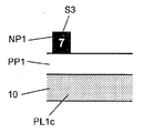
도 2에 관하여 기술된 구조화된 데이터층을 구비하는 ROM 광 저장 매체를 제작하기 위한 스탬퍼 제작을 위한 제 1 비금속 마스터는 예를 들면, 도 3에 대하여 기술된 바와 같이, 제 1 방법을 이용함으로써 제작될 수 있다. 도 3a에 있어서, 비금속 기판(10)을 포함하는 플레이트(PL1a)의 일부가 단면도로 도시되며, 이 기판(10)은 포지티브 포토 레지스트(PP1)에 의해 덮이고, 그리고 네거티브 포토 레지스트(NP1)에 의해 덮힌다. 기판(10)은 예를 들면 유기 기판 또는 실리콘(Si), 또는 SiO2기판이다. 포토 레지스트(PP1 및 NP1)는 다음 성질을 가져야 하는데, 즉 첫 번 째로, 레지스트(NP1)를 제거하기 위해 사용가능한 액체 용매는 레지스트(PP1)에 영향을 미치지 않아야 하며, 두 번째로는, 레지스트(PP1)를 제거하기 위해 사용가능한 액체 용매는 포토 레지스트(NP1)에 영향을 미치지 않아야 한다. The first non-metallic master for fabricating the stamper for making the ROM optical storage medium having the structured data layer described with reference to Figure 2 can be fabricated, for example, by using the first method, as described for Figure 3 . 3A, a part of a plate PL1a including a
도 3b의 제 1 단계에서, 네거티브 포토 레지스트(NP1)는 도 2에 도시된 바와 같이, 특히 융기부(PM)와 유사한 포지티브 마크(7)를 제작하기 위한 마스터링 머신을 이용하여 조명된다. 조명 이후, 네거티브 포토 레지스트(NP1)는 도 3b의 플레이트(PL1b)로 표시된 바와 같이, 제 1 나선(S3)을 위한 데이터 구조를 포함한다. 다음 단계에 있어서, 제 1 용매가 플레이트(PL1b) 상에 가해져, 노출되지 않은 영역에서의 네거티브 포토 레지스트(NP1)를 제거한다. 따라서, 도 3c에 예시된 바와 같이, 융기부(7)를 갖는 포지티브 마크와 공간으로 구성되는 제 1 나선(S3)을 포함하는 플레이트(PL1c)가 획득된다. In the first step of figure 3b, the negative photoresist NP1 is illuminated using a mastering machine to produce a
도 3d의 추가 단계에서, 포지티브 포토 레지스트(PP1)가 마스터링 머신을 이용하여 조명되어, 도 2에 도시된 바와 같이, 제 2 나선(S4)에 대하여, 특히 피트(NM)와 유사한 네거티브 마크를 제작한다. 따라서, 포지티브 포토 레지스트(PP1)를 갖는 층은 도 3d에서 단순화된 방식으로 표시된 바와 같이, 플레이트(PL1d)인 데이터 구조를 포함한다. 다음 단계에서, 제 2 용매가 가해져 노출 영역에서의 포지티브 포토 레지스트(PP1)를 제거한다. 따라서, 도 3e에 도시된 바와 같이, 각각의 피트(8)인 포지티브 마크를 구비하는 제 2 나선(S4)을 포함하는 플레이트(PL1e)가 획득된다. 플레이트(PL1e)는 알려진 방식으로 ROM 디스크를 제작하기 위한 2개의 나선(S3, S4)을 포함하는 데이터 구조를 이제 포함한다. 플레이 트(PL1e)는 예를 들면, 알려진 바와 같이, 스탬퍼로서 사용되거나 스탬퍼를 제작하기 위해 사용될 수 있다.In a further step of figure 3d, the positive photoresist PP1 is illuminated using a mastering machine to produce a negative mark similar to the pit NM especially for the second spiral S4, as shown in Figure 2 And make them. Thus, the layer with the positive photoresist PP1 comprises a data structure that is a plate PL1d, as shown in a simplified manner in Fig. 3d. In the next step, a second solvent is added to remove the positive photoresist < RTI ID = 0.0 > PP1 < / RTI > Thus, as shown in FIG. 3E, a plate PL1e including a second spiral S4 having a positive mark as each
도 2에 따른 데이터 구조를 포함하는 ROM 광 저장 매체를 제작하기 위하여 스탬퍼 제작을 위한 제 2 비금속 마스터의 제 2 제작 방법이 도 4에 대하여 이제 기술된다. 도 4a에 있어서, 물질(M2)에 의해 덮이는 기판(20)을 포함하는 플레이트(PL2a)가 도시되고, 이 물질은 감광적이지 않지만, 그러나 액체 용매에서 용해가능하고, 제 5 용매로 언급된다. 기판(20)은 예를 들면, 유리 기판 또는 실리콘(Si), 또는 SiO2 기판이다. 이 물질(M2)은 네거티브 포토 레지스트(NP2)에 의해 덮인다. 제 2 단계에 있어서, 네거티브 포토 레지스트(NP2)를 갖는 플레이트(PL2a)는 도 4b에 도시된 바와 같이, 포지티브 마크(7)를 제작하기 위한 마스터링 머신을 이용하여 조명된다. 조명 이후, 제 3 용매가 가해져 노출되지 않은 영역에서의 네거티브 포토 레지스트(NP2)를 제거한다. 이 결과가 도 4c에 도시된다. 제 3 용매는 그러므로 여전히 완전하게 유리 기판(20)을 덮고 있는 물질(M2)에 영향을 미치지 않아야 한다. A second fabrication method of a second non-metal master for fabricating a stamper to fabricate a ROM optical storage medium comprising the data structure according to Fig. 2 will now be described with respect to Fig. In Figure 4a a plate PL2a is shown comprising a
추가 단계에서, 도 4c에 도시된 바와 같이 포지티브 마크(7)를 갖는 플레이트(PL2c)가 포지티브 포토 레지스트(PP2)로 코팅되어 플레이트(PL2d)를 획득해야 한다. 이후, 포토 레지스트(PP2)를 갖는 플레이트(PL2d)는 마스터링 머신을 이용하여 조명되어 도 4d에 도시된 바와 같이, 포지티브 마크(7)를 구비하는 트랙 사이의 네거티브 마크(8)를 구비하는 트랙을 제작한다. 이후, 제 4 용매가 가해져 노출된 영역에서의 포지티브 포토 레지스트(PP2)를 제거한다. 그 결과, 플레이트(PL2e)가 도 4e에 도시된다. In a further step, a plate PL2c having a
이후, 제 5 용매를 사용함으로써, 물질(M2)의 덮이지 않은 부분을 제거하기 위한 에칭 프로세스가 적용된다. 포지티브 포토 레지스트(PP2)에 영향을 미치지 않도록 제 5 에칭 용매가 선택된다. 따라서, 피트(8)가 물질(M2)에서 획득되며, 이는 도 4f에 도시된 바와 같이, 플레이트(PL2f)를 제작한다. 최종 단계에서, 제 6 용매가 사용되어 포지티브 포토 레지스트(PP2)의 나머지 부분을 제거하며, 따라서 유리 마스터(PL2g)가 도 4g에 도시된 바와 같이 획득되며, 이로부터 도 2에 따른 판독 전용 광 저장 매체의 제작을 위한 스탬퍼가 제작될 수 있다. Thereafter, by using the fifth solvent, an etching process for removing the uncovered portion of the material M2 is applied. A fifth etching solvent is selected so as not to affect the positive photoresist PP2. Thus, a
플레이트(PL2g)의 포지티브 마크(7), 및 대응하게 네거티브 마크(8)는 약 300 - 500nm의 넓은 트랙 피치를 가지며, 이 피치는 블루 레이 시스템 광학계를 포함하는 픽업 유닛을 이용함으로써 각 광 저장 매체를 위한 트래킹 조정을 특히 허용한다. 이후, 네거티브 피트(7)와 포지티브 피트(8)를 구비하는 트랙 사이에서의 트랙 피치는 블루 레이 픽업의 광 해상도 한계 미만인 150 - 250nm의 범위 내에 있다. 이러한 방법으로 제작된 스탬퍼를 이용함으로써, 따라서 방사 치수(radial dimension)에서 약 2배의 증가된 데이터 밀도를 포함하는 ROM 디스크가 제작될 수 있다. The
포토 레지스트(NP2, PP2) 및 물질(M2)은 다음의 성질을 가져야 하는데, 즉 포토 레지스트(NP2)를 제거하기 위해 사용된 제 3 용매는 물질(M2)에 영향을 미치지 못한다. 포토 레지스트(PP2)의 조명된 부분을 제거하기 위해 사용된 제 4 용매 는 부분적으로 물질(M2)을 용해할 수 있다. 물질(M2)을 에칭하기 위해 사용된 제 5 용매는 포토 레지스트(PP2)에 영향을 미치지 않아야 한다. 포토 레지스트(PP2)의 조명되지 않은 부분을 제거하기 위해 사용된 제 6 용매는 기판(20), 물질(M2) 및 포토 레지스트(NP2)의 포지티브 마크(7)에 영향을 미치지 않아야 한다. The photoresists NP2 and PP2 and the material M2 should have the following properties: the third solvent used to remove the photoresist NP2 does not affect the material M2. The fourth solvent used to remove the illuminated portion of the photoresist PP2 may partially dissolve the material M2. The fifth solvent used to etch the material M2 should not affect the photoresist PP2. The sixth solvent used to remove the unexposed portions of the photoresist PP2 should not affect the
도 3에 관하여 기술된 방법과 비교하여 본 방법의 이점은 상이한 포토 레지스트와 상이한 포토 레지스트(M2)를 이용하기 위해 더 많은 자유가 얻어지는 점이다. 원리상, 물질(M2)이 감광적일 것이 요구되지 않는다. 물질(M2)과 기판(20)에 대하여, 예를 들면 유리, SiO2, 또는 Si가 사용될 수 있다. 더욱이, 물질(M2)을 생략하는 것이 특히 가능하다. 이 경우에서, 피트(8)는 기판(20)에 직접 에칭된다. An advantage of the method compared to the method described with reference to Figure 3 is that more freedom is obtained to utilize a photoresist M2 that is different from the different photoresist. In principle, it is not required that the material M2 be photosensitive. With respect to the material (M2) and the
도 2에 따른 데이터 구조를 포함하는 ROM 광 저장 매체를 제작하는 스탬퍼 제작을 위한 금속 마스터 제작 방법이 도 5에 대하여 설명된다. 이 방법에 대하여, 또한 포지티브 피트를 포함하는 나선과 네거티브 피트를 포함하는 이웃하는 나선이 수개의 연속 단계로 제작된다. 마스터의 제작은 네거티브 포토 레지스트(NP3)로 덮인, 예를 들면, 유리 기판 또는 실리콘(Si) 또는 SiO2 기판과 같은, 비금속 기판(30)을 포함하는 플레이트(PL3a)로 시작한다. 제 1 단계에서, 플레이트(PL3a)의 포토 레지스트(NP3)가 마스터링 머신을 이용하여 조명되어 도 5b에 도시된 바와 같이, 포지티브 마크(8)를 제작한다. 조명 이후, 제 7 용매가 가해져 도 5c에 도시된 바와 같이, 융기부와 유사한 마크(8)를 제작하기 위해 노출되지 않은 영역에서 포토 레지스트(NP3)를 제거한다. 포지티브 마크(8) 사이의 트랙 피치는 예를 들면 300nm - 500nm의 범위 내에 있다. A method of manufacturing a metal master for manufacturing a stamper for manufacturing a ROM optical storage medium including the data structure according to Fig. 2 will be described with reference to Fig. For this method, a spiral containing a positive pit and a neighboring spiral containing a negative pit are also fabricated in several successive steps. Preparation of Master begins with a plate (PL3a), including,
이후, 스퍼터링 및 전기 도금 방법이 도 5d에 도시된 바와 같이, 금속(ME)으로 플레이트(PL3c)를 덮음으로써, 예를 들면 니켈 마스터와 같은 금속 마스터인 플레이트 PL3d를 만들기 위해 사용된다. 이후, 다음 단계에서, 마크(8)의 나머지 포토 레지스트(NP3)와 함께 기판(30)이 종래의 마스터링에서와 같은 동일한 원리를 사용함으로써 제거된다. 이후, 플레이트(PL3c)의 포지티브 마크(8)에 상응하는, 사전 기록된 정보를 포함하는, 각각의 피트(9)인 네거티브 마크(9)를 포함하는 금속 기판(ME1)이 얻어진다. The sputtering and electroplating process is then used to make the plate PL3d, which is a metal master such as a nickel master, for example, by covering the plate PL3c with a metal ME, as shown in Fig. 5D. Then, in the next step, the
금속 기판(ME1)은 이후 금속 마스터를 제작하기 위한 기판으로서 사용된다. 다음 단계에 있어서, 금속 기판(ME1)은 예를 들면 1 -5 mm의 매우 얇은층으로 덮여, 포토 레지스트의 접착을 향상시키고 금속 기판(ME1)과 포토 레지스트 사이에서의 화학 반응을 감소시킨다. 이후, 금속 마스터(ME1)는 포토 레지스트(NP3)와 유사한 네거티브 포토 레지스트(NP4)로 덮여, 도 5e의 플레이트(PL3e)를 얻는다. 추가 단계에서, 플레이트(PL3e)의 포토 레지스트(NP4)가 마스터링 머신을 이용하여 조명되어 도 5f에 도시된 바와 같이, 포지티브 마크(7)를 갖는 트랙을 제작한다. 추가 단계에서, 제 8 용매가 가해져 노출되지 않은 영역에서 네거티브 포토 레지스트(NP4)를 제거하여 도 5g에 도시된 바와 같이, 각각의 융기부인 포지티브 마크(7)를 갖는 트랙을 얻는다. The metal substrate ME1 is then used as a substrate for manufacturing a metal master. In the next step, the metal substrate ME1 is covered with a very thin layer, for example 1 -5 mm, to improve the adhesion of the photoresist and reduce the chemical reaction between the metal substrate ME1 and the photoresist. Thereafter, the metal master ME1 is covered with a negative photoresist NP4 similar to the photoresist NP3 to obtain the plate PL3e of Fig. 5E. In a further step, the photoresist (NP4) of the plate PL3e is illuminated using a mastering machine to produce a track with a
따라서, 금속 마스터(ME2)가 얻어지는데, 즉 플레이트(PL3g)가 되며, 이 플레이트로부터 스탬퍼가 "부" - "모" 및 "자" 스탬퍼를 위해 마스터-스탬퍼 복사로 이루어지는 동일한 방식으로 제작될 수 있다. 최종 스탬퍼는 유리하게는 예를 들면 150nm - 250nm의 포지티브 마크(7)와 네거티브 마크(9) 사이의 작은 트랙 피치를 갖는다. 특히 금속(ME)로서 니켈이 사용될 수 있지만, 그러나 다른 금속 또는 합금이 또한 사용될 수 있다. 포지티브 마크(7)와 네거티브 마크(9)를 갖는 트랙이 특히 2개의 나선으로서 배열되되, 제 1 나선은 오직 포지티브 마크(7)만을 포함하고, 제 2 나선은 오직 네거티브 마크(9)만을 포함한다. Thus, a metal master ME2 is obtained, that is to say a plate PL3g from which the stamper can be made in the same way as a master-stamper copy for "negative" - " have. The final stamper advantageously has a small track pitch between the
플레이트(PL1b, PL2b 또는 PL3d)의 제작 이후, 마스터링 머신으로부터 플레이트(PL1b, PL2b 또는 PL3d)를 제거하여 플레이트(PL1b, PL2b) 또는 금속 기판(ME1)을 얻는 것이 필수적일 수 있다. 플레이트(PL1b, PL2b) 또는 금속 기판(ME1)이 다시 마스터링 머신으로 넣어지는 경우, 플레이트(PL1b, PL2b) 또는 금속 기판(ME1)을 정확하게 재정렬시키는 것일 필수적이다. 이는 플레이트(PL1b 또는 PL2b) 상의 피트(7) 또는 금속 기판(ME1)에 제작된 피트(9)를 이용함으로써 달성될 수 있는데, 즉 도 5에 도시된 방법에 대하여, 현재의 피트는 현재의 피트(8) 사이의 중간에 각각의 융기부인 새로운 마크(7)를 제작하기 위해 정확하게 마스터링 빔을 정렬하기 위해 사용될 수 있는 푸시-풀 신호를 제작한다. 추가적으로는, 피트(9)의 데이터 신호에 기반된 PLL이 사용되어 새로운 마크(7)의 마스터링 동안 선형 속도를 안정화시킬 수 있다. 이는 피트 길이 편차 및 따라서 관련된 지터 기여를 감소시킨다. After the fabrication of the plates PL1b, PL2b or PL3d it may be necessary to remove the plates PL1b, PL2b or PL3d from the mastering machine to obtain the plates PL1b, PL2b or the metal substrate ME1. It is essential that the plates PL1b and PL2b or the metal substrate ME1 are put back into the mastering machine to correctly rearrange the plates PL1b and PL2b or the metal substrate ME1. This can be achieved by using the
Super-RENS ROM 디스크에 대하여, 최적 기하학적 형태(geometry)는 각각 피트 및 융기부인 포지티브 및 네거티브 마크에 대하여 상이할 수 있다는 것을 언급 해야 한다. 이는 super-RENS 효과를 제작하는 정확한 물리적 현상에 의존한다. 이러한 상황하에서, 포토 레지스트 또는 물질의 상이한 두께를 이용함으로써 개별적으로 포지티브 마크 및 네거티브 마크의 깊이, 높이 및 기하학적 형태를 최적화하는 것이 유용할 수 있는데, 즉 NP1 및 PP1은 도 3을 참조하고, NP2 및 M2는 도 4를 참조하고, NP3 및 NP4는 도 5를 참조하고/하거나 마스터링 동안 상이하나 기록 전략을 사용하자. 더욱이, 일부 경우에서, 포지티브 마크와 네거티브 마크를 마스터링하기 위해 상이한 파장을 사용하는 것이 유리할 수 있다. For Super-RENS ROM disks, it should be noted that the optimal geometry may be different for the positive and negative marks, which are pits and ridges, respectively. This depends on the exact physical phenomenon of producing the super-RENS effect. Under such circumstances, it may be useful to optimize the depth, height and geometry of the positive and negative marks individually by using different thicknesses of photoresist or material, i.e. NP1 and PP1 refer to FIG. 3, M2 refer to FIG. 4, NP3 and NP4 refer to FIG. 5 and / or during mastering, but use a write strategy. Moreover, in some cases, it may be advantageous to use different wavelengths to master the positive and negative marks.
도 5에 관하여 기술된 방법은 오직 네거티브 포토 레지스트(NP3, NP4)만이 사용되어야 하는 이점을 갖는다. 원칙적으로, 동일한 포토 레지스트가 포토 레지스트(NP3 및 NP4)를 위해 사용될 수 있다. 제 1 방법과 제 2 방법에서 사용된 용매에 관하여 필수적인 것과 같이, 제 7 용매와 제 8 용매에서의 가해성(solvability)에 관해 2개의 포토 레지스트(NP3 및 NP4)에 대하여 어떤 특별한 제한도 필요하지 않다. 제 7 용매 및 제 8 용매에 관한 유일한 제한은 이들이 기판(30)과 금속 기판(ME1)에 영향을 미치지 않아야 한다는 점이다. 더욱이, Ni대신에, 또한 다른 금속 또는 금속 합금이 사용될 수 있다. The method described with reference to Figure 5 has the advantage that only negative photoresists (NP3, NP4) should be used. In principle, the same photoresist can be used for the photoresist (NP3 and NP4). No special restrictions are required for the two photoresists (NP3 and NP4) as to the solvability in the seventh and eighth solvents, as is necessary for the solvents used in the first and second methods not. The only limitation with respect to the seventh solvent and the eighth solvent is that they should not affect the
또한 본 발명의 다른 실시예는 본 발명의 기술 사상 및 범위를 벗어나지 않으면서도 당업자에 의해 만들어질 수 있다. 본 발명은 실시예에 기술된 바와 같이, 판독 전용(ROM) 광 저장 매체뿐만 아니라 기록가능하고 재기록 가능한 광 저장 매체에 대하여 이용될 수 있다. 이전에 기술된 방법은 특히 도 1에 관하여 기술된 Super-RENS 광 디스크를 제작하기 위해 사용될 수 있지만, 그러나 또한 블루 레이 형 디스크를 제작하기 위해서도 사용될 수 있다. 그러므로, 본 발명은 이후 첨부된 청구항에 귀속한다.Other embodiments of the invention may be made by those skilled in the art without departing from the spirit and scope of the invention. The present invention may be used for read-only (ROM) optical storage media as well as for recordable and rewritable optical storage media, as described in the embodiments. The previously described method can be used to produce the Super-RENS optical disc described in particular with reference to FIG. 1, but can also be used to produce Blu-ray discs. Therefore, the present invention is hereinafter referred to as the appended claims.
본 발명은 기판층, 이 기판층 상의 트랙 내에 배열되는 마크 및 공간 구조를 갖는 판독 전용 데이터층 및 덮개층을 포함하는 광 저장 매체, 및 이 광 저장 매체의 각 제작에 이용 가능하다. 또한, 이 광 저장 매체는 특히 고 데이터 밀도로 데이터를 저장하기 위한 초 해상도 근접장 구조(super-resolution near-field structure)를 갖는 마스크층을 포함한다. The present invention is applicable to each manufacture of optical storage media and optical storage media comprising a substrate layer, a read only data layer having a mark and space structure arranged in tracks on the substrate layer, and a cover layer. The optical storage medium also includes a mask layer having a super-resolution near-field structure for storing data, especially at high data densities.
여기서, 하나의 트랙은 포지티브 마크를 포함하고, 인접 트랙은 네거티브 마크를 포함한다. 이 트랙은 특히 나선처럼 배열되는데, 여기서 하나의 나선은 오직 포지티브 마크만을 갖는 트랙을 포함하고, 이웃 나선은 오직 네거티브 마크를 갖는 트랙을 포함한다. Here, one track includes a positive mark, and adjacent tracks include a negative mark. This track is arranged in particular as a spiral, where one spiral contains tracks with only positive marks and the neighbor spiral contains tracks with only negative marks.
Claims (14)
Applications Claiming Priority (5)
| Application Number | Priority Date | Filing Date | Title |
|---|---|---|---|
| EP06122316 | 2006-10-16 | ||
| EP06122316.0 | 2006-10-16 | ||
| EP06123931.5 | 2006-11-13 | ||
| EP06123931 | 2006-11-13 | ||
| PCT/EP2007/060826 WO2008046777A1 (en) | 2006-10-16 | 2007-10-11 | Optical storage medium comprising tracks with positive and negative marks, and stampers and production methods for manufacturing of the optical storage medium |
Publications (2)
| Publication Number | Publication Date |
|---|---|
| KR20090064399A KR20090064399A (en) | 2009-06-18 |
| KR101492520B1 true KR101492520B1 (en) | 2015-02-23 |
Family
ID=38867079
Family Applications (1)
| Application Number | Title | Priority Date | Filing Date |
|---|---|---|---|
| KR20097006433A KR101492520B1 (en) | 2006-10-16 | 2007-10-11 | Optical storage medium comprising tracks with positive and negative marks, and stampers and production methods for manufacturing of the optical storage medium |
Country Status (8)
| Country | Link |
|---|---|
| US (1) | US8023395B2 (en) |
| EP (1) | EP2074617B1 (en) |
| JP (1) | JP5202534B2 (en) |
| KR (1) | KR101492520B1 (en) |
| CN (1) | CN101536095B (en) |
| AT (1) | ATE499680T1 (en) |
| DE (1) | DE602007012738D1 (en) |
| WO (1) | WO2008046777A1 (en) |
Families Citing this family (8)
| Publication number | Priority date | Publication date | Assignee | Title |
|---|---|---|---|---|
| US8182966B2 (en) * | 2008-12-23 | 2012-05-22 | General Electric Company | Data storage devices and methods |
| US8493832B2 (en) | 2009-04-28 | 2013-07-23 | Thomson Licensing, LLC | Optical storage medium having different dimension of recorded marks and spaces on different tracks |
| EP2246854A1 (en) * | 2009-04-28 | 2010-11-03 | Thomson Licensing | Optical storage medium comprising tracks with different modulation codes, and respective apparatus for reading of data |
| EP2299442A1 (en) * | 2009-09-17 | 2011-03-23 | Thomson Licensing | Optical storage medium comprising a data layer with an inverted pit/land data structure |
| EP2325840A1 (en) | 2009-11-23 | 2011-05-25 | Thomson Licensing | Optical storage medium comprising an active layer designed as an anti-reflective layer |
| EP2372709A1 (en) | 2010-03-30 | 2011-10-05 | Thomson Licensing | Optical storage medium comprising a data layer with reduced track pitch and an inverted/non-inverted mark/space data structure |
| CN107797396B (en) * | 2016-09-07 | 2020-12-25 | 深圳莱宝高科技股份有限公司 | Method for manufacturing alignment mark of conductive film |
| JP7164931B2 (en) | 2019-03-08 | 2022-11-02 | キャタピラー エス エー アール エル | Lubrication piping arrangement structure in construction machinery |
Citations (3)
| Publication number | Priority date | Publication date | Assignee | Title |
|---|---|---|---|---|
| US6570840B1 (en) * | 2000-04-26 | 2003-05-27 | Optical Disc Corporation | Figure of merit in optical recording structures |
| KR20050093899A (en) * | 2004-03-19 | 2005-09-23 | 삼성전자주식회사 | Method for manufacturing recorded master, recorded master and information storage medium being manufactured by the method |
| US7102986B2 (en) * | 2000-02-28 | 2006-09-05 | Fujitsu Limited | Optical disk |
Family Cites Families (19)
| Publication number | Priority date | Publication date | Assignee | Title |
|---|---|---|---|---|
| US4430401A (en) * | 1979-06-13 | 1984-02-07 | Discovision Associates | Method for producing a recording disc stamper |
| US5553051A (en) * | 1987-09-04 | 1996-09-03 | Hitachi, Ltd. | Increased intensity optical recording medium with adjacent grooves of different optical depth and a method and apparatus for reproducing the same |
| JP3361078B2 (en) * | 1991-02-15 | 2003-01-07 | ソニー株式会社 | Reproduction method of optical recording medium |
| JPH06150394A (en) * | 1992-11-12 | 1994-05-31 | Matsushita Electric Ind Co Ltd | Production of master optical disk |
| JP3040894B2 (en) * | 1993-03-10 | 2000-05-15 | 松下電器産業株式会社 | Optical disk substrate and optical disk |
| JPH11250504A (en) * | 1998-02-27 | 1999-09-17 | Sony Corp | Optical recording medium and its manufacture |
| US6706358B1 (en) * | 1998-04-09 | 2004-03-16 | Seagate Technology Llc | Storage disk comprising depressions and /or raised features |
| JP3615054B2 (en) * | 1998-06-04 | 2005-01-26 | ソニー株式会社 | Optical recording medium |
| JP2000256889A (en) * | 1999-03-05 | 2000-09-19 | Sony Corp | Production of disk for duplication of stamper and production of optical recording medium |
| CN1956066B (en) | 2000-01-14 | 2010-05-12 | 松下电器产业株式会社 | Optical disc and optical disc address reading apparatus and method |
| US6804189B2 (en) * | 2000-04-07 | 2004-10-12 | Tosoh Corporation | Near field optical recording medium |
| US6930969B2 (en) * | 2000-10-26 | 2005-08-16 | Pioneer Corporation | Optical recording medium applicable for improved servo control |
| JP2003338053A (en) * | 2002-05-20 | 2003-11-28 | Canon Inc | Optical recording medium |
| JP2005216462A (en) * | 2004-02-02 | 2005-08-11 | Sharp Corp | Optical information recording medium |
| JP2005310329A (en) * | 2004-04-26 | 2005-11-04 | Sony Corp | Optical recording medium, reproducing apparatus, and tracking servo method |
| JP2006012285A (en) * | 2004-06-25 | 2006-01-12 | Tdk Corp | Magnetic recording medium and method of manufacturing magnetic recording medium |
| JP3916636B2 (en) * | 2005-02-15 | 2007-05-16 | Tdk株式会社 | Magnetic recording medium, magnetic recording / reproducing apparatus |
| JP4058445B2 (en) * | 2005-11-25 | 2008-03-12 | Tdk株式会社 | Stamper, imprint method, and information recording medium manufacturing method |
| JP4705530B2 (en) * | 2006-08-07 | 2011-06-22 | 株式会社リコー | Optical recording medium and substrate thereof, and stamper for molding the substrate |
-
2007
- 2007-10-11 CN CN2007800385002A patent/CN101536095B/en not_active Expired - Fee Related
- 2007-10-11 EP EP07821193A patent/EP2074617B1/en not_active Not-in-force
- 2007-10-11 US US12/311,714 patent/US8023395B2/en not_active Expired - Fee Related
- 2007-10-11 KR KR20097006433A patent/KR101492520B1/en not_active IP Right Cessation
- 2007-10-11 WO PCT/EP2007/060826 patent/WO2008046777A1/en active Application Filing
- 2007-10-11 AT AT07821193T patent/ATE499680T1/en not_active IP Right Cessation
- 2007-10-11 DE DE602007012738T patent/DE602007012738D1/en active Active
- 2007-10-11 JP JP2009532774A patent/JP5202534B2/en not_active Expired - Fee Related
Patent Citations (3)
| Publication number | Priority date | Publication date | Assignee | Title |
|---|---|---|---|---|
| US7102986B2 (en) * | 2000-02-28 | 2006-09-05 | Fujitsu Limited | Optical disk |
| US6570840B1 (en) * | 2000-04-26 | 2003-05-27 | Optical Disc Corporation | Figure of merit in optical recording structures |
| KR20050093899A (en) * | 2004-03-19 | 2005-09-23 | 삼성전자주식회사 | Method for manufacturing recorded master, recorded master and information storage medium being manufactured by the method |
Also Published As
| Publication number | Publication date |
|---|---|
| US8023395B2 (en) | 2011-09-20 |
| EP2074617B1 (en) | 2011-02-23 |
| WO2008046777A1 (en) | 2008-04-24 |
| JP5202534B2 (en) | 2013-06-05 |
| ATE499680T1 (en) | 2011-03-15 |
| EP2074617A1 (en) | 2009-07-01 |
| CN101536095A (en) | 2009-09-16 |
| JP2010507182A (en) | 2010-03-04 |
| CN101536095B (en) | 2011-06-08 |
| DE602007012738D1 (en) | 2011-04-07 |
| KR20090064399A (en) | 2009-06-18 |
| US20100195476A1 (en) | 2010-08-05 |
Similar Documents
| Publication | Publication Date | Title |
|---|---|---|
| KR101492520B1 (en) | Optical storage medium comprising tracks with positive and negative marks, and stampers and production methods for manufacturing of the optical storage medium | |
| US20100027406A1 (en) | Optical storage medium comprising tracks with different width and respective production method | |
| US20080187861A1 (en) | Master Substrate and Method of Manufacturing a High-Density Relief Structure | |
| EP2106609B1 (en) | Optical storage medium with a mask layer providing a super resolution near field effect, and respective manufacturing method | |
| JP3991534B2 (en) | Optical information recording medium | |
| JP4337080B2 (en) | Optical information recording medium | |
| JP4337069B2 (en) | Optical information recording medium | |
| JP4491804B2 (en) | Optical information recording medium | |
| JP4491807B2 (en) | Optical information recording medium | |
| JP4491806B2 (en) | Optical information recording medium | |
| JP4491803B2 (en) | Optical information recording medium | |
| JP4491802B2 (en) | Optical information recording medium | |
| JP4491805B2 (en) | Optical information recording medium | |
| JP4609781B2 (en) | Optical information recording medium | |
| JP2008504635A (en) | Optical data storage medium and manufacturing method thereof | |
| JP4600434B2 (en) | Optical information recording medium | |
| EP2372709A1 (en) | Optical storage medium comprising a data layer with reduced track pitch and an inverted/non-inverted mark/space data structure | |
| JP2004192775A (en) | Optical information recording medium and its manufacturing method | |
| JP2008071465A (en) | Optical information recording medium |
Legal Events
| Date | Code | Title | Description |
|---|---|---|---|
| A201 | Request for examination | ||
| E902 | Notification of reason for refusal | ||
| E902 | Notification of reason for refusal | ||
| E701 | Decision to grant or registration of patent right | ||
| GRNT | Written decision to grant | ||
| LAPS | Lapse due to unpaid annual fee |