KR101171663B1 - Touch panel with both elevation of view trait and printing layer - Google Patents
Touch panel with both elevation of view trait and printing layer Download PDFInfo
- Publication number
- KR101171663B1 KR101171663B1 KR1020110008822A KR20110008822A KR101171663B1 KR 101171663 B1 KR101171663 B1 KR 101171663B1 KR 1020110008822 A KR1020110008822 A KR 1020110008822A KR 20110008822 A KR20110008822 A KR 20110008822A KR 101171663 B1 KR101171663 B1 KR 101171663B1
- Authority
- KR
- South Korea
- Prior art keywords
- layer
- oxide layer
- indium tin
- tin oxide
- substrate
- Prior art date
Links
Images


Classifications
-
- G—PHYSICS
- G06—COMPUTING; CALCULATING OR COUNTING
- G06F—ELECTRIC DIGITAL DATA PROCESSING
- G06F3/00—Input arrangements for transferring data to be processed into a form capable of being handled by the computer; Output arrangements for transferring data from processing unit to output unit, e.g. interface arrangements
- G06F3/01—Input arrangements or combined input and output arrangements for interaction between user and computer
- G06F3/03—Arrangements for converting the position or the displacement of a member into a coded form
- G06F3/041—Digitisers, e.g. for touch screens or touch pads, characterised by the transducing means
- G06F3/0412—Digitisers structurally integrated in a display
-
- B—PERFORMING OPERATIONS; TRANSPORTING
- B32—LAYERED PRODUCTS
- B32B—LAYERED PRODUCTS, i.e. PRODUCTS BUILT-UP OF STRATA OF FLAT OR NON-FLAT, e.g. CELLULAR OR HONEYCOMB, FORM
- B32B33/00—Layered products characterised by particular properties or particular surface features, e.g. particular surface coatings; Layered products designed for particular purposes not covered by another single class
-
- B—PERFORMING OPERATIONS; TRANSPORTING
- B32—LAYERED PRODUCTS
- B32B—LAYERED PRODUCTS, i.e. PRODUCTS BUILT-UP OF STRATA OF FLAT OR NON-FLAT, e.g. CELLULAR OR HONEYCOMB, FORM
- B32B2457/00—Electrical equipment
- B32B2457/20—Displays, e.g. liquid crystal displays, plasma displays
- B32B2457/208—Touch screens
-
- G—PHYSICS
- G06—COMPUTING; CALCULATING OR COUNTING
- G06F—ELECTRIC DIGITAL DATA PROCESSING
- G06F2203/00—Indexing scheme relating to G06F3/00 - G06F3/048
- G06F2203/041—Indexing scheme relating to G06F3/041 - G06F3/045
- G06F2203/04103—Manufacturing, i.e. details related to manufacturing processes specially suited for touch sensitive devices
Landscapes
- Engineering & Computer Science (AREA)
- General Engineering & Computer Science (AREA)
- Theoretical Computer Science (AREA)
- Human Computer Interaction (AREA)
- Physics & Mathematics (AREA)
- General Physics & Mathematics (AREA)
- Position Input By Displaying (AREA)
Abstract
본 발명은 시인성 향상과 인쇄층을 겸비한 터치패널에 관련된다.
구성에 있어서, 글래스 ? PC(폴리카보네이트) ? PMMA(폴리메타메틸아크릴) 중에서 하나를 주재로 하는 기판(10); 및 상기 기판(10)의 일면에 인쇄층(21)과 산화니오븀층(22)을 증착하고; 산화니오븀층(22)의 상면에 다시 굴절율이 다른 물질을 다층으로 증착하여 형성되는 전도층(30);을 포함하여 이루어지는 것을 특징으로 한다.
이에 따라, 경량화/슬림화의 추세에 부응하면서 시인성을 향상하여 다양한 제품으로 응용이 가능하도록 하고, 더불어 인쇄층까지 일괄 형성하여 추가 제조공정의 번거로움까지 제거시킨 효과가 있다.The present invention relates to a touch panel having both a visibility improvement and a printed layer.
In the composition, the glass? PC (polycarbonate) A substrate 10 based on one of PMMA (polymethacryl); Depositing a printed layer (21) and a niobium oxide layer (22) on one surface of the substrate (10); And a conductive layer 30 formed on the upper surface of the niobium oxide layer 22 by depositing a material having a different refractive index in multiple layers.
Accordingly, in response to the trend of light weight / slim, it is possible to improve the visibility and to be applied to various products, and also to form a printed layer collectively to remove the hassle of additional manufacturing process.
Description
본 발명은 글래스, PC(폴리카보네이트), PMMA(폴리메타메틸아크릴) 등의 기판을 이용한 터치패널에 관한 것으로, 더욱 상세하게는 경량화/슬림화의 추세에 부응하면서 1, 2차에 걸친 산화인듐주석층(ITO)의 형성으로 다양한 기능향상과 함께 시인성을 향상하여 다양한 제품으로 응용이 가능하도록 하고, 더불어 인쇄층까지 일괄 형성하여 추가 제조공정의 번거로움까지 제거시킨 시인성 향상과 인쇄층을 겸비한 터치패널에 관한 것이다.The present invention relates to a touch panel using a substrate such as glass, PC (polycarbonate), PMMA (polymethylmethylacryl), and more particularly, to meet the trend of light weight and slimming, indium tin oxide in the first and second stages. Formation of layer (ITO) improves visibility and improves visibility, enables application to various products, and also forms printed layers collectively to improve visibility and eliminates the hassle of additional manufacturing processes. It is about.
통상적으로 터치패널은 저항막 방식, 정전용량 방식, 초음파 방식, 탄성파 방식, 적외선 방식 등으로 구분되며, 이 중에서 현재 저항막 방식과 정전용량 방식이 주종을 이루고 있다. In general, the touch panel is classified into a resistive film type, a capacitive type, an ultrasonic type, an acoustic wave type, an infrared type, and the like, and the resistive type and the capacitive type are mainly used.
저항막 방식은 작동 신뢰성과 안정성이 높아 TV, 모니터, 노트북 PC, 카네비게이션, 게임기기, 백색가전, PDA, 전자사전, 휴대전화, 캠코더 등에 폭 넓게 사용된다. 다만, 전도성 물질이 코팅된 유리나 필름 위에 전도성 물질이 코팅된 필름을 적층한 구조이므로, 상하판 사이 공기층(Air Gap)에 의한 난반사 현상으로 야외 시인성이 불량하고, 유리를 사용하는 경우 표면의 유연성이 결여되어 응용분야의 확산에 장애가 된다. 정전용량 방식은 인체의 정전기를 감지해 구동하는 방식으로서 내구성이 강하고 반응시간이 짧으며 투과성이 좋아 일부 산업용, 카지노 게임기로부터 최근 휴대폰으로 적용범위가 확대되고 있다. 반면, 펜을 이용하거나 장갑 낀 손으로 작동되지 않고 비교적 고가인 단점을 지닌다. The resistive type is widely used in TVs, monitors, notebook PCs, car navigation systems, gaming devices, white appliances, PDAs, electronic dictionaries, mobile phones and camcorders due to its high reliability and stability. However, since the conductive material is coated on the glass or the film coated with the conductive material is laminated structure, the outdoor visibility is poor due to the diffuse reflection phenomenon by the air gap between the upper and lower plates, the surface flexibility when using glass Lack of barriers to the proliferation of applications. The capacitive method is a method of sensing and driving static electricity of the human body, which has a strong durability, a short response time, and a high permeability, and has recently been applied to mobile phones from some industrial and casino game machines. On the other hand, it does not operate with a pen or gloved hand and has a relatively expensive disadvantage.
어느 방식에 있어서 제품의 용도에 부합된 품질과 생산성의 유지는 향후 시장성을 판가름하는 중요한 요인으로 인식되고 있으며, 적용제품의 다양화로 글래스(유리)를 도입할 필요성도 있으나 현실적인 난관이 따른다.In some ways, the maintenance of quality and productivity consistent with the use of the product is recognized as an important factor in determining the future marketability, and there is a necessity to introduce glass (glass) due to the diversification of the applied product, but there are practical difficulties.
한국 등록특허공보 제0681157호의 "정전용량 방식의 터치 패널의 구조 및 그 제조방법"에 의하면 『은 페이스트로 형성된 선형성 패턴, 실드패턴 및 오버코팅막이 형성되는 글래스 기판과; 상기 글래스 기판의 전면부에 ITO 또는 ATO로 형성하여 터치패널에 터치되는 물제의 터치위치를 정확하게 검출할 수 있는 투명도전막과; 상기 글래스 기판의 배면부를 ITO로 형성하여 노이즈를 차폐하는 투명도전막과; 상기 투명도전막의 배면부에 은 페이스트로 형성되어 노이즈를 감쇄시키기 위한 실드패턴과; 상기 투명도전막의 전면부에 은 페이스트로 형성하여 터치패널에서 구조적으로 발생하는 왜곡된 신호로부터 선형성으로 보정하기 위해 형성되며, 터치패널에 만들어지는 전압을 일정하게 분배시켜 선형성을 확보하는 선형성 패턴과; 상기 선형성 패턴 상부면과 투명도전막의 표면 위에 산화규소층(SiO2) 계 코팅 용액으로 균일하게 스핀 코팅되어 터치패널의 전도 코팅층을 보호하고 노이즈를 감쇄시킬 수 있는 오버 코팅막과; 상기 선형성 패턴에 전원을 공급하기 위한 전극에 테일의 단자를 솔더링으로 접합하여 연결되어 있는 유연하고 플래트한 테일; 로 구성』된다.According to Korean Patent Publication No. 0681157, "The structure of a capacitive touch panel and its manufacturing method", "A glass substrate formed with a linear pattern, a shield pattern and an overcoating film formed of silver paste; A transparent conductive film formed of ITO or ATO on the front surface of the glass substrate so as to accurately detect a touch position of a material touched by the touch panel; A transparent conductive film for shielding noise by forming a back portion of the glass substrate with ITO; A shield pattern formed of silver paste on the rear surface of the transparent conductive film to reduce noise; A linear pattern formed by using a silver paste on the front surface of the transparent conductive film to correct linearly from a distorted signal structurally generated in the touch panel, and uniformly distributing a voltage generated in the touch panel to ensure linearity; Silicon oxide layer (SiO 2 ) on the upper surface of the linear pattern and the surface of the transparent conductive film An overcoat layer uniformly spin-coated with a system coating solution to protect the conductive coating layer of the touch panel and reduce noise; A flexible and flat tail connected by soldering a terminal of a tail to an electrode for supplying power to the linear pattern; It consists of.
한국 등록특허공보 제908225호는 『하부 절연체층, 상기 하부 절연체층의 상면에 터치부 패턴으로 형성된 하부 투명 전도 산화막 층, 및 상기 하부 투명 전도 산화막 층으로부터 상기 하부 절연체층의 가장자리까지 전기적 신호의 인출을 위한 연결 패턴으로 형성된 하부 금속 증착 코팅층으로 이루어진 하부 패드; (중략) 상기 전기적 신호의 인출을 위한 연결 패턴은 전부에 대하여 상기 투명 전도 산화막 층과 상기 금속 증착코팅층의 2중층 구조』를 제안한다. 이는 종래에 ITO층으로부터 외부로의 인출을 위한 연결 패턴으로 실버페이스트를 적용한 공정보다 저가의 재료와 간단한 공정으로 제작이 가능하다고 밝힌다.Korean Patent Publication No. 908225 discloses `` a lower insulator layer, a lower transparent conductive oxide layer formed in a touch pattern on an upper surface of the lower insulator layer, and drawing out an electrical signal from the lower transparent conductive oxide layer to the edge of the lower insulator layer. A lower pad made of a lower metal deposition coating layer formed in a connection pattern for forming the lower pad; (Omitted) proposes a double layer structure of the transparent conductive oxide film layer and the metal deposition coating layer for all the connection patterns for the electrical signal extraction. This reveals that it is possible to manufacture a material with a lower cost and a simpler process than a process in which silver paste is applied as a connection pattern for drawing out from the ITO layer to the outside.
그러나 상기한 종래 기술들에 의하면 어느 정도 양산성과 내구성을 향상할 수 있기는 하지만, 정전용량 방식의 유리 기판에 적용 시 높은 굴절율의 발휘에 한계가 있어 다양한 제품으로 응용하기 어려운 애로가 있었고, 그 외 인쇄층을 터치패널의 초기 공정에 포함시켜 제조해내는 종래 기술은 거의 전무한 문제가 있었다.However, according to the above-mentioned conventional technologies, although mass productivity and durability can be improved to some extent, when applied to a capacitive glass substrate, there is a limitation in exhibiting high refractive index, which makes it difficult to apply to various products. There is almost no problem in the prior art of manufacturing a printed layer by including it in an initial process of a touch panel.
이에 따라 본 발명은 경량화/슬림화의 추세에 부응하면서 1, 2차에 걸친 산화인듐주석층(ITO)의 형성함으로써 다양한 기능향상과 함께 시인성을 향상하여 다양한 제품으로 응용이 가능하도록 하고, 더불어 인쇄층까지 일괄 형성하여 추가 제조공정의 번거로움까지 제거시킨 터치패널을 제공하려는데 그 목적이 있다.Accordingly, the present invention responds to the trend of light weight and slimming, and by forming the indium tin oxide layer (ITO) in the first and second stages to improve the visibility and various functions to be applied to a variety of products, and the printed layer It is an object of the present invention to provide a touch panel in which a batch is formed to remove the hassle of additional manufacturing processes.
이러한 목적을 달성하기 위해 본 발명은 터치패널에 있어서: 글래스, PC(폴리카보네이트), PMMA(폴리메타메틸아크릴) 중에서 하나를 주재로 하는 기판; 및 상기 기판의 일면에 인쇄층과 산화니오븀(![]()
![]()
![]()
![]()
삭제delete
또한, 본 발명에 따르면 상기 전도층은 저굴절율을 지닌 산화규소층(SiO2)과 고굴절율을 지닌 1차 산화인듐주석층(ITO; Indium Tin Oxide)을 차례로 증착하고, 이어 절연막층 및 2차 산화인듐주석층(ITO; Indium Tin Oxide)을 추가로 더 형성하는 것을 특징으로 한다.Further, according to the present invention, the conductive layer deposits a silicon oxide layer (SiO 2 ) having a low refractive index and a primary indium tin oxide (ITO) layer having a high refractive index in turn, followed by an insulating layer and a secondary layer. Indium Tin Oxide (ITO) is further characterized in that it further forms.
한편, 이에 앞서 본 명세서 및 특허청구범위에 사용된 용어나 단어는 통상적이거나 사전적인 의미로 한정해서 해석되어서는 아니 되며, 발명자는 그 자신의 발명을 가장 최선의 방법으로 설명하기 위해 용어의 개념을 적절하게 정의할 수 있다는 원칙에 입각하여 본 발명의 기술적 사상에 부합하는 의미와 개념으로 해석되어야만 한다. 따라서 본 명세서에 기재된 실시예와 도면에 도시된 구성은 본 발명의 가장 바람직한 일 실시예에 불과할 뿐이고, 본 발명의 기술적 사상을 모두 대변하는 것은 아니므로, 본 출원시점에 있어서 이들을 대체할 수 있는 다양한 균등물과 변형예들이 있을 수 있음을 이해하여야 한다.On the other hand, the terms or words used in the present specification and claims are not to be construed as limiting the ordinary or dictionary meanings, the inventors should use the concept of the term in order to explain the invention in the best way. It should be interpreted as meanings and concepts corresponding to the technical idea of the present invention based on the principle that it can be properly defined. Therefore, the embodiments described in the present specification and the configuration shown in the drawings are only the most preferred embodiments of the present invention, and do not represent all of the technical ideas of the present invention, and various alternatives may be substituted at the time of the present application. It should be understood that there may be equivalents and variations.
이상의 구성 및 작용에서 설명한 바와 같이, 본 발명에 따른 터치패널의 적층 구조는 정전용량 방식의 터치패널에 기판을 적용함에 있어 경량화/슬림화의 추세에 부응하면서 1, 2차에 걸친 산화인듐주석층(ITO)의 형성함으로써 다양한 기능향상과 함께 시인성을 향상하여 다양한 제품으로 응용이 가능한 효과가 있고, 또 인쇄층까지 일괄 형성함으로써 추가 제조공정의 번거로움까지 제거시킨 효과가 있다.As described in the above configuration and operation, the laminated structure of the touch panel according to the present invention meets the trend of light weight / slim in applying the substrate to the capacitive touch panel, while the indium tin oxide layer is applied to the first and second layers ( By forming ITO), it is possible to apply various products by improving visibility and improving various functions. In addition, it is possible to eliminate the inconvenience of additional manufacturing process by collectively forming the printed layer.
도 1은 본 발명에 따른 터치패널의 주요구조를 적층상태로 나타낸 구성도
도 2는 본 발명에 따른 터치패널의 주요구조 중 제2 산화인듐주석층이 제거된 상태의 상부 구성도
도 3(a)는 본 발명에 따른 제1 산화인듐주석층 상부에 PR노광처리 및 에칭액의 살포과정을 보여주는 상태도(a-a'선 단면 포함)
도 3(b)는 제1 산화인듐주석층 상면에 PR층이 제거되는 모습의 구성도
도 4(a)는 본 발명에 따른 절연막층 상부에 PR노광처리 과정을 보여주는 상태도
도 4(b)는 절연막층 상부의 에칭액 살포과정(도 4a의 b-b'선 단면 포함) 및 절연막층이 형성된 상태의 구성도
도 5(a)는 절연막층 상부에 제2 산화인듐주석층이 적층된 구성도
도 5(b)는 도 5a의 c-c'선 단면도이다.1 is a configuration diagram showing the main structure of the touch panel according to the present invention in a laminated state
2 is a top configuration diagram of a state in which the second indium tin oxide layer is removed from the main structure of the touch panel according to the present invention;
Figure 3 (a) is a state diagram showing the PR exposure process and the spraying process of the etching solution on the first indium tin oxide layer according to the present invention (including a-a 'line cross section)
Figure 3 (b) is a configuration diagram of the PR layer is removed on the upper surface of the first indium tin oxide layer
Figure 4 (a) is a state diagram showing a PR exposure process on the insulating film layer according to the present invention
FIG. 4 (b) is a schematic view of the etching solution spraying process (including the cross section of b-b 'line in FIG. 4a) and the insulating film layer formed thereon.
5 (a) is a configuration diagram in which a second indium tin oxide layer is stacked on the insulating film layer
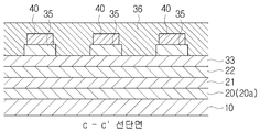
(B) is sectional drawing along the line c-c 'of FIG. 5a.
이하, 첨부된 도면에 의거하여 본 발명의 실시예를 상세하게 설명하면 다음과 같다.Hereinafter, exemplary embodiments of the present invention will be described in detail with reference to the accompanying drawings.
본 발명은 터치패널에 관련되는 것으로, 특히 전도층의 일부를 증착에 의하여 형성하는 방식에 관련된다. 일예로, 정전용량 방식의 경우 기판(10) 상에 전도층(30)을 증착으로 형성한 본 발명의 구성에 이어서, 연결구 ? 도트 스페이서 ? 도선을 지닌 도전층을 접합한 다음 마지막으로 필름을 접합하는 공정을 택할 수 있다. The present invention relates to touch panels, and more particularly to the manner in which a portion of the conductive layer is formed by vapor deposition. For example, in the case of the capacitive method, following the configuration of the present invention in which the conductive layer 30 is formed by vapor deposition on the
다른 예로, 기판(10) 상에 전도층(30)을 증착으로 형성한 상태에서 상기와 다른 적층 구조를 택할 수 있다. 어느 방식이든 다양한 기능향상과 함께 시인성이 개선되면 다양한 제품으로의 응용성이 높아진다.As another example, in the state in which the conductive layer 30 is formed by vapor deposition on the
본 발명의 개략적인 공정순서를 살피기에 앞서 설명의 편의를 위해 글래스, PC(폴리카보네이트), PMMA(폴리메타메틸아크릴) 등의 기판(10) 가운데 셀 글래스(Cell Glass) 기판을 중심으로 하여 설명하기로 한다. Prior to reviewing the schematic process sequence of the present invention, for convenience of explanation, the description will be made based on a cell glass substrate among the
본 발명의 개략적인 공정순서를 살피면, 세정 전 셀 글래스(Cell Glass) 기판(10)을 적재하는 준비단계, 셀글래스를 세정기에 투입하는 세정단계, 셀글래스를 캐리어에 로딩하는 단계, 인쇄층이 형성된 셀글래스를 진공챔버에 진입시키는 단계, 플라즈마 형성에 의해(![]()
![]()
본 발명에 따르면 글래스, PC(폴리카보네이트), PMMA(폴리메타메틸아크릴) 중에서 하나를 주재로 하는 기판(10)이 사용되며, 기판(10)은 소정의 전처리를 거쳐 물성을 개선해야 한다. 통상적으로 물성의 개선은 물리적 방식, 열적 방식, 화학적 방식 중에서 선택된다.According to the present invention, a
이때, 상기 글래스 기판(10)의 경우에는 소다라임 글래스 또는 고리라 글래스 중에서 선택되고, 화학강화층(20)을 구비한다. 소다라임 글래스와 고리라 글래스는 디스플레이 제품에 요구되는 물성을 구비하므로 적절하지만, 반드시 이에 국한되는 것은 아니고 다양한 글래스 소재의 기판(10)을 적용할 수 있다. 글래스의 균열은 미세한 균열과 마찰력에 의하여 발생하므로, 열처리 또는 화학적 처리에 의한 표면강화로 이를 개선할 수 있다. 열처리 방식의 경우 용융점 이상의 온도구배에서 임시적으로 응력개선이 발생하고, 글래스가 단순한 평면이면서 일정치 이상의 두께로 되어야 한다. 반면 화학적 방식에 의한 화학강화층(20)은 글래스의 모양이나 두께에 관계없이 고강도를 구현할 수 있다.At this time, in the case of the
상기한 화학강화층(20)은 400~500℃ 내외의 질산칼륨용액에 2~8시간 내외로 침지하여 형성되는 것을 특징으로 한다. 화학강화는 이온교환과정에 의한 것으로서 유리의 용융점 보다 낮은 온도에서 수행된다. 글래스를 400~500℃ 내외의 질산칼륨용액에 2~8시간 내외로 동안 침지한 상태로 두면 글래스 표면의 Na이온과 용액의 K이온이 상호 교환되면서 전자기력에 의한 수축으로 강화가 발생한다. 그리고 화학강화층(20)의 바람직한 온도와 질산칼륨용액의 침지시간은 터치패널의 기능에 따라 달라지는데, 예를 들어 화학강화층(20)의 온도를 420℃로 하고 질산칼륨용액에 3시간가량을 침지시킬 수도 있지만, 온도를 450℃로 하고 질산칼륨용액에 4~5시간동안 침지시킬 수도 있는데, 이것은 터치패널의 특성에 따라 화학강화층(20)의 강도를 달리 처리하는데서 오는 결과라 할 수 있다. The chemically strengthened
이와 같은 화학강화층(20)을 지닌 기판(10)은 열처리에 의한 것보다 약 8배정도 높은 강도를 발휘하고, 처리 중에 비틀림 등의 변형이 적을뿐더러 색상 및 빛 투과율 특성을 그대로 유지한다.The
그리고 상기 PC(폴리카보네이트), PMMA(폴리메타메틸아크릴) 등의 기판(10)의 경우에는 아크릴수지계의 하드코팅층을 기판(10) 일면에 형성함으로써 후술할 인쇄층(21)과의 친화력이 강화된다.In the case of the
한편, 본 발명에 따르면 상기 기판(10)의 일면에 인쇄층(21)과 산화니오븀층(22)을 차례로 증착하는데, 이러한 증착과정을 보다 상세하게 설명한다. Meanwhile, according to the present invention, the printed
우선 인쇄층(21)은 기판(10)의 어느 일면 중 임의의 적정지점에 그림 ? 문자 ? 도형 등을 새길 수 있는 층을 말하는데, 종래에는 터치패널이 완성되고 나서 별도의 공정을 통해 인쇄층을 형성해 왔기 때문에 제조공정이 무척 번잡한 문제가 있었으나 본 발명에서는 기판(10) 위에 인쇄층(21)을 먼저 형성한 후 다양한 기능향상과 함께 시인성을 높이기 위한 전도층(30) 등을 차례로 형성한다. First, the
인쇄층(21)의 형성은 유기물의 경우에는 스퀴즈 프린팅(printing) 방법 등으로, 무기물의 경우에는 진공증착 메탈방법 등으로 형성하는데, 인쇄층(21)을 무기물로 형성할 경우에는 일반적으로 진행하는 340℃ 내외의 가열조건에서 작업수행을 해도 별 문제없지만 유기물로 인쇄층(21)을 형성할 경우에 일반적으로 진행하는 340℃ 내외의 가열조건에서는 작업수행이 약간 어려운 문제가 있다. The
즉, 인쇄층(21) 상면에 적층될 산화규소층(33)이나 산화인듐주석층(35)은 진공증착방법에 있어서 바람직한 온도범위인 340℃ 내외의 가열조건에서도 깔끔하게 작업을 수행할 수 있으나 유기물로 인쇄층(21)을 형성할 경우에는 270℃의 온도가 되면 타버릴 수 있는 경우도 발생한다. 따라서 인쇄층(21)은 가급적 250℃±50℃의 가열온도범위 내에서 형성하는 것이 좋고, 그 결과 산화니오븀층(22)과 후술할 산화규소층(33)이나 산화인듐주석층(35) 역시 250℃ 내외의 온도범주 속에서 진공증착을 하는 것이 바람직한데, 이때 발생되는 또 다른 문제는 250℃ 내외의 낮은 온도에서 진공 증착할 경우에 산화인듐주석층(35)의 저항치가 높아 터치패널로서의 기능 수행이 어렵다는 점이다. 즉, 산화인듐주석층(35)을 340℃ 내외로 진공증착(sputtering) 시키면 터치패널로서는 가장 바람직한 80~250Ω의 저항치를 갖게 되지만 250℃ 내외로 진공증착 시키면 평균 400~500Ω의 저항치를 갖게 되어 터치패널로서의 기능 수행이 어렵게 된다. That is, the
이를 좀 더 상세히 설명하면, 산화인듐주석층(35)을 250℃ 내외로 진공증착(sputtering) 시키면 산화인듐주석층(35)의 물질들이 불안정하고 유동적인 상태가 되어 결정화가 되지 않아 저항치가 400~500Ω으로 높아진다. 즉, 터치패널 기능이 제대로 수행되기 위해서는 80~250Ω의 저항치가 바람직하지만 산화인듐주석층(35)이 250℃ 내외에서 진공증착 되는 한, 산화인듐주석층(35)의 물질들이 결정되지 않아 저항치가 400~500Ω으로 높아지는 문제가 뒤따른다. 따라서 250℃ 내외의 가열온도 범위에서 형성해야 할 인쇄층(21)의 형성으로 말미암아 발생되는 400~500Ω의 저항치를 80~250Ω의 저항치로 떨어뜨리기 위해서는 산화인듐주석층(35)의 불안정 상태를 안정화 상태로 변화시켜야 하고, 안정화 상태 모드로 만들기 위해서는 180~500℃의 진공챔버 내에 산화인듐주석층(35)까지 모두 적층된 상태의 터치패널을 진공챔버 내에 재투입해서 10~50분가량을 재차 통과시키면 산화인듐주석층(35)의 물질들이 쉽게 결정화되면서 저항치가 80~250Ω 내외로 떨어져 다양한 소비자의 욕구에 부응할 수 있게 된다.In more detail, when the indium
그리고 인쇄층(21)이 형성된 후에 다시 산화니오븀층(22)을 차례로 증착하는데, 플라즈마에 의한 ![]()
![]()
![]()
![]()
![]()
![]()
한편, 진공챔버의 온도를 340℃ 내외로 설정한 뒤 전술한 PC나 PMMA 기판(10) 상에 인쇄층(21) 및 산화인듐주석층(35)을 증착하더라도 80~250Ω 내외의 저항치를 가지면서 PC나 PMMA의 기판(10) 및 인쇄층(21)이 타버리지 않도록 할 수는 있지만, 생산성 저하 및 불량품 발생 우려가 있으므로 가급적 진공챔버의 온도를 250℃ 내외로 설정하여 소비자가 요구하는 다양한 저항치의 터치패널용 기판을 제조할 수 있게 된다. 참고로 인쇄층(21)과 산화니오븀(22), 후술할 산화규소층(33)은 저항치의 상승 또는 하강과는 아무런 관계가 없을 뿐 아니라 250℃ 내외의 온도에서 진공증착해도 순조롭게 증착됨을 부연한다. On the other hand, after setting the temperature of the vacuum chamber to about 340 ℃ and depositing the
되돌아가서 상기 기판(10)의 일면에 인쇄층(21)을 형성한 후에는 산화니오븀층(22)을 추가로 진공 증착하여 시인성을 높이기 위한 전도층(30)의 형성이 용이하도록 한다. After returning and forming the printed
본 발명에 따르면 상기 산화니오븀층(22)의 상면에 굴절율이 다른 물질을 다층으로 증착하여 전도층(30)을 형성한다. 전도층(30)은 전술한 글래스, PC, PMMA 등의 소재 중에서 선택되는 기판(10)을 진공챔버(Vacuum chamber)에 수용하고 소정의 가스 분위기에서 증착(sputtering)을 통하여 형성된다. According to the present invention, a conductive layer 30 is formed by depositing multiple layers of materials having different refractive indices on the upper surface of the
이때, 상기 전도층(30)은 저굴절율을 지닌 산화규소층(33)과, 고굴절율을 지닌 제1 산화인듐주석층(35), 절연막층(40) 및 제2 산화인듐주석층(36)을 차례로 증착하여 형성된다. 이와 같이 기판(10) 상에 산화규소층(33), 산화인듐주석층(ITO; Indium Tin Oxide) 및 절연막층(40)을 형성하는 본 발명의 증착과정을 보다 상세하게 설명한다.In this case, the conductive layer 30 includes a
우선, 셀 글래스 재료의 수입검사 및 자재수량을 확인한 다음 카세트에 적재한다. 한 열에 적재 가능한 수량은 대략 62개 내외이며(그 이상, 이하도 가능), 첫 번째와 마지막 칸은 비워서 취급불량을 방지한다. 세정 카세트 3열 60매씩 적재가 완료되면 전체적으로 외관 상태를 확인한다. 세정기 투입대기 장소로 이동하여 투입대기 선반에 적재한다. 물론 이 공정의 이전 또는 직후에 화학강화를 거쳐 화학강화층(20)을 형성한 셀 글래스(또는 기판)를 사용해야 한다. First, the import inspection and material quantity of the cell glass material are checked and loaded into the cassette. Approximately 62 can be loaded in a row (more and less), and the first and last spaces are empty to prevent mishandling. When loading of 60 sheets of 3 rows of cleaning cassettes is completed, check the appearance as a whole. Move to the washing machine's waiting place and load it on the loading stand shelf. Of course, the cell glass (or substrate) in which the
다음으로, 적재된 셀글래스 재료를 세정기에 넣어 세정작업을 수행한다. 이때 세정 온도는 60℃ 내외로 하고 세정 시간은 약 45분 정도로 하는 것이 적당하다. 이러한 수치는 사용하는 셀글래스 재료의 기타 조건에 따라 조절될 수 있다.Next, the loaded cell glass material is put in a washing machine to perform a washing operation. At this time, it is appropriate that the cleaning temperature is about 60 ℃ and the cleaning time is about 45 minutes. These values can be adjusted according to other conditions of the cell glass material used.
다음으로, 세정 공정을 마친 셀글래스 재료는 진공챔버로 진입하기 위해 캐리어(Carrier)에 로딩된다. 로딩 시에는 코팅 유효 범위 존(Zone) 내에 유지하도록 투입되는 수량을 제한한다.Next, the cell glass material having been cleaned is loaded into a carrier to enter the vacuum chamber. When loading, the quantity to be put in to keep in the coating effective range zone is limited.
다음으로, 셀글래스 재료를 진공챔버에 진입시킨다. 이때 진공챔버 분위기 온도는 250℃ 내외의 적정온도로 설정한다. 이후 마그네트론 스퍼터링(Magnetron Sputtering) 방식에 의한 플라즈마 스퍼터링 처리를 수행한다. 마그네트론 스퍼터링은 타겟에 가해지는 바이어스 전압(DC, RF)에 의하여 타겟과 실드(Shield) 혹은 타겟과 기판(Substrate) 사이에서 생성될 수 있는 플라즈마를 타겟에 붙어 있는 영구자석을 이용하여 타겟 근처에 집중시키고, 타겟 표면과 플라즈마 사이의 전위차에 의해 가속된 이온들이 타겟 표면과 충돌하여 이차 전자방출을 일으킴과 동시에 타겟 표면에서 스퍼터링을 일으키고, 스퍼터링된 중성의 원자들이 기판으로 날아가 박막을 형성하는 원리로 작동된다. Next, the cell glass material is put into a vacuum chamber. At this time, the vacuum chamber atmosphere temperature is set to an appropriate temperature of about 250 ℃. Thereafter, plasma sputtering is performed by a magnetron sputtering method. Magnetron sputtering focuses near the target using a permanent magnet attached to the target, which can generate plasma between the target and the shield or the target and the substrate due to bias voltages (DC, RF) applied to the target. Ions accelerated by the potential difference between the target surface and the plasma collide with the target surface to cause secondary electron emission, sputtering at the target surface and sputtered neutral atoms fly to the substrate to form a thin film. do.
다음으로, 아르곤(Ar) 플라즈마에 의한 SiO2 코팅처리를 수행하여 산화규소층(33)을 형성한다. 이때 코팅되는 박막두께는 250Å 정도를 유지하는 것이 바람직하다. 그리고 산화니오븀층(22) 위에 다시 산화규소층(33)을 형성하는데, 산화규소층(SiO2) 대신 산화알루미늄(Al2O3)이나 산화실리콘(SiNx) 등의 저 굴절물질을 사용하여 증착할 수도 있다. 한편 SiO2 코팅 시 방법은 RF 파워의 제어방식으로는 캐소드(Cathode) 4개를 사용하는 것이 바람직하다. 캐소드 개수 및 배치되는 위치는 진공챔버의 구조에 따라 달라질 수 있으며, 본 발명에 최적화되는 캐소드는 셀글래스 재료에 대향하는 위치에서 일정한 등 간격을 유지하는 4개를 선정한다. 캐소드 수가 적으면 박막 형성이 미흡해질 우려가 있고, 너무 많으면 두께의 균일한 제어가 곤란하다. 이에 따라 코팅에 의한 투과율을 90% 이상으로 향상시킬 수 있다. 이어서 상온에서 증착된 산화규소층(SiO2)의 막강도 향상시키기 위해 플라즈마 처리작업을 수행한다. 그리고 상기한 SiO2 코팅방법 대신 염화마그네슘(MGF2)을 E빔(일렉트론 빔)에 녹여서 증착하는 방법도 가능하나 SiO2 코팅 처리방법이 더 바람직한 것으로 사료된다.Next, the
다음으로, 코팅된 산화규소층(SiO2)의 셀글래스 재료에 직류파워 제어방식에 의해 120±50Å 두께로 ITO를 코팅하여 제1 산화인듐주석층(35)을 형성한다. ITO 코팅 처리 시에는 아르곤 및 산소 가스의 압력제어에 의해 ITO 성막의 저항 균일도를 5% 이내로 유지하도록 한다. 이러한 제어 방식은 통상의 장치를 사용할 수 있다. 분위기의 조건을 정밀 제어하는 전용의 장치를 사용한다. Next, ITO is coated on the cell glass material of the coated silicon oxide layer (SiO 2 ) to a thickness of 120 ± 50 μs by a DC power control method to form a first indium
다음으로, 제1 산화인듐주석층(35) 위에 절연막층(40)을 형성하고 제2 산화인듐주석층(36)을 또 다시 형성하는데, 제1 산화인듐주석층(35) 위에 절연막층(40)을 형성하는 공정은 다음과 같다.Next, an insulating
도 3a에서 보듯이 제1 산화인듐주석층(35)(35′) 상부 전체 면에 PR층(포토 레지스트층; Photoresist)을 코팅한 후 PR층(감광성 수지액)을 부분적으로 박리하기 위한 마스킹과 함께 PR 노광처리 과정을 거쳐 공지의 박리액(剝離液)을 PR층에 살포하면, 노광 처리되지 아니한 부분의 PR층(35a, 도 3a의 ㉠부분)과 ㉠부분의 PR층(35a) 바로 밑에 있는 제1 산화인듐주석층(35′, 도 3a의 ㉡부분) 부분이 깨끗하게 박리된다. 즉, 도 3b에서 보는 바와 같이 인쇄층(21), 산화니오븀층(22), 산화규소층(33)이 차례로 적층되어져 있는 기판(10) 위에 PR층의 일부분(도 3a의 ㉢부분, 35b)과 제1 산화인듐주석층(35, 도 3a의 ㉣부분)이 남게 된다. 그런 다음, 다시 제1 산화인듐주석층(35) 위에 있는 PR층(35b, 도 3b의 ㉢부분)만을 재차 박리시키면 제1 산화인듐주석층(35, 도 3b의 ㉣부분)만 남게 된다. 그 후, PR층(35a)(35b)이 제거된 제1 산화인듐주석층(35, 도 3b의 ㉣부분) 위에 절연막층(40)을 브릿지 형태로 형성하되, 제1 산화인듐주석층(35)의 양 가장자리 일부분을 남겨 두고 절연막층(40)을 덧씌우는데, 이러한 절연막층(40)은 상기한 PR층(Photoresist층)의 코팅 물질과 동일하고, 절연막층(40)의 형성 과정은 전술한 도 3a와 도 3b의 경우와 비슷하다.Masking for partially peeling the PR layer (photosensitive resin liquid) after coating the PR layer (photoresist) on the entire upper surface of the first indium tin oxide layer 35 (35 '), as shown in FIG. When the known exfoliating liquid is sprayed onto the PR layer through the PR exposure process, the
이를 좀 더 상술하면, 제1 산화인듐주석층(35) 상부 전체 면에 전술한 PR층(포토 레지스트층, 40a)을 다시 재코팅 하는데, 이 PR층(포토 레지스트층, 40a)의 일부가 바로 절연막층(40)으로 이용된다. 즉, 제1 산화인듐주석층(35) 상부 전체 면에 코팅된 PR층(40a)을 부분적으로 박리하기 위한 PR 노광처리 과정(도 4a 참조)을 거쳐 에칭액(etching液)을 PR층에 살포하면, 도 4b에서 보듯이 노광 처리된 부분의 절연막층(40, 도 4b의 ㉤부분)을 제외한 나머지 부분의 PR층(40a, ㉥부분)이 깨끗하게 박리되며, 이러한 박리과정을 거치게 되면 도 4b에서 보듯이 제1 산화인듐주석층(35) 위에 브릿지 형태의 절연막층(40)이 형성된다.In more detail, the above-described PR layer (
그런 다음, 제1 산화인듐주석층(35)과 절연막층(40) 상부 면에 제2 산화인듐주석층(36)을 또 다시 형성하는데, 이렇게 될 경우 절연막층(40)이 덧씌워지지 아니한 제1 산화인듐주석층(35)의 양 가장자리 부분과 제2 산화인듐주석층(36)의 일 측면 부분은 또 다른 별도의 공정을 통해 서로 접면하게 된다. 결국, 제1 산화인듐주석층(35)과 제2 산화인듐주석층(36)을 상하로 형성하면서 부분적으로 접면시키되, 절연막층(40)을 중간에 형성하여 제1 산화인듐주석층(35)의 원활한 전기적 기능과 다양한 기능이 유지되도록 하면서 제2 산화인듐주석층(36)과의 과도한 전극적 충돌 내지 파괴현상을 방지할 수 있다. 즉, 상하 2층으로 구성된 제1, 제2의 산화인듐주석층(35)(36) 사이에 절연막층(40)을 중간에 형성함으로써 전기적 기능의 활성화 면적을 드높이면서 과도한 전극적 충돌 등을 피할 수 있는 이점이 있게 된다.Then, the second indium
그리고 제1 산화인듐주석층(35)과 절연막층(40) 상부 면에 제2 산화인듐주석층(36)을 또 다시 형성하는 경우에는 전술한 세정공정과 ITO 코팅 공정, 진공챔버 온도 및 저항치 등이 모두 동일하게 적용된다.In the case where the second indium
다음으로, 이온빔으로 표면 처리하여 ITO 박막의 안정화를 통한 저항 경시변화율 감소를 달성할 수 있다. 또한, 산화인듐주석층(35)(36)의 물질들을 안정화시키는 방법은 이미 위에서 자세히 언급한 바가 있으므로 추가적인 상세 설명은 생략한다.Next, the surface treatment with an ion beam can be achieved to reduce the resistance change over time through the stabilization of the ITO thin film. In addition, a method of stabilizing the materials of the indium
이렇게 제조된 셀글래스 재료의 터치패널을 캐리어에서 탈착한 후 외관 검사과 특성 검사를 수행한다. 외관 검사는 표면의 스크래치, 이물, 오염, 핀홀 등을 육안으로 검사하는 것이고, 특성 검사는 전기저항, 투과율, 막 두께, 내열성, 내마모성을 측정하는 것이다.The touch panel of the cell glass material thus prepared is detached from the carrier and then inspected for appearance and characteristics. Appearance inspection is to visually inspect scratches, foreign substances, contamination, pinholes, etc. on the surface, and property inspection is to measure electrical resistance, transmittance, film thickness, heat resistance, and wear resistance.
통상 91% 정도의 투과율을 지니는 기판(10)에 산화인듐주석층(35)(36)만 적층하면 투과율이 86%로 저하되지만, 산화규소층(33)과 산화인듐주석층(35)(36)을 적층하면 약 90%내외의 투과율로 회복된다. 이와 같이 본 발명은 기판(10)의 상면에 산화규소층(34)의 저굴절 물질 및 산화인듐주석층(35)(36)의 고굴절 물질을 순차적으로 적층함으로써 다양한 기능향상과 함께 터치패널의 시인성을 향상한다. When only the indium tin oxide layers 35 and 36 are laminated on the
본 발명은 기재된 실시예에 한정되는 것은 아니고, 본 발명의 사상 및 범위를 벗어나지 않고 다양하게 수정 및 변형할 수 있음은 이 기술의 분야에서 통상의 지식을 가진 자에게 자명하다. 따라서 그러한 변형예 또는 수정예들은 본 발명의 특허청구범위에 속한다 해야 할 것이다.
It is apparent to those skilled in the art that the present invention is not limited to the described embodiments, and that various modifications and variations can be made without departing from the spirit and scope of the present invention. It is therefore intended that such variations and modifications fall within the scope of the appended claims.
10: 기판 20: 화학강화층
20a: 하드코팅층 21: 인쇄층
22: 산화니오븀층 30: 전도층
33: 산화규소층 35: 제1 산화인듐주석층
36: 제2 산화인듐주석층 40: 절연막층10: substrate 20: chemically strengthened layer
20a: hard coat layer 21: printed layer
22: niobium oxide layer 30: conductive layer
33: silicon oxide layer 35: first indium tin oxide layer
36: second indium tin oxide layer 40: insulating film layer
Claims (6)
글래스, PC(폴리카보네이트), PMMA(폴리메타메틸아크릴) 중에서 하나를 주재로 하는 기판(10); 및
상기 기판(10)의 일면에 인쇄층(21)과 산화니오븀층(22)을 차례로 증착하고;
상기 산화니오븀층(22)의 상면에 굴절율이 다른 물질을 다층으로 증착하여 형성되는 전도층(30);을 포함하여 이루어지며,
상기 글래스 기판(10)은 소다라임 글래스 또는 고리라 글래스 중에서 선택되고, 기판(10)의 일면에 화학강화층(20)을 구비하되, 화학강화층(20)은 400~500℃ 내외의 질산칼륨용액에 2~8시간 내외로 침지하여 형성되는 것을 특징으로 하는 시인성 향상과 인쇄층을 겸비한 터치패널.In the touch panel:
A substrate 10 based on one of glass, PC (polycarbonate), and PMMA (polymethacryl); And
Depositing a printed layer (21) and a niobium oxide layer (22) on one surface of the substrate (10) in sequence;
And a conductive layer 30 formed by depositing a material having a different refractive index in multiple layers on the upper surface of the niobium oxide layer 22.
The glass substrate 10 is selected from soda lime glass or ring glass, and provided with a chemical strengthening layer 20 on one surface of the substrate 10, the chemical strengthening layer 20 is a potassium nitrate solution of about 400 ~ 500 ℃ Touch panel combines visibility and print layer, which is formed by dipping in about 2 to 8 hours.
상기 전도층(30)은 저굴절율을 지닌 산화규소층(33)과 고굴절율을 지닌 제1산화인듐주석층(35)을 증착하되, 상기 제1산화인듐주석층(35)의 양 가장자리를 제외한 상면부에 절연막층(40)을 형성하고, 제1산화인듐주석층(35) 및 절연막층(40) 상부의 전체 면에 제2산화인듐주석층(36)을 추가 형성하되, 제2산화인듐주석층(36)의 일측부는 절연막층(40)이 없는 제1산화인듐주석층(35)의 양 측 가장자리 부와 상호 연접되도록 함을 특징으로 하는 시인성 향상과 인쇄층을 겸비한 터치패널.The method of claim 1,
The conductive layer 30 deposits a silicon oxide layer 33 having a low refractive index and a first indium tin oxide layer 35 having a high refractive index, except for both edges of the first indium tin oxide layer 35. An insulating layer 40 is formed on the upper surface, and a second indium tin oxide layer 36 is further formed on the entire surface of the first indium tin oxide layer 35 and the insulating layer 40. One side of the tin layer 36 is connected to both edge portions of the first indium tin oxide layer 35 without the insulating layer 40, the touch panel having both a visibility improvement and a print layer.
상기 PC 또는 PMMA의 기판(10)은 일면에 하드코팅층(20a)을 구비하고, 그 상면에 인쇄층(21)과 산화니오븀층(22) 및 전도층(30)을 차례로 증착하는 것을 특징으로 하는 시인성 향상과 인쇄층을 겸비한 터치패널.The method of claim 1,
The substrate 10 of the PC or PMMA has a hard coating layer 20a on one surface thereof, and a printed layer 21, a niobium oxide layer 22, and a conductive layer 30 are sequentially deposited on the upper surface thereof. Touch panel with improved visibility and printed layer.
상기 기판(10)은 상면에 산화인듐주석층(35)을 증착시킨 다음, 약 180~500℃내외의 진공챔버 내에 약 10~50분가량 재투입하여 저항치를 크게 낮출 수도 있음을 특징으로 하는 시인성 향상과 인쇄층을 겸비한 터치패널.The method according to claim 1 or 3,
The substrate 10 is deposited on the upper surface of the indium tin oxide layer 35, and then re-injected for about 10 to 50 minutes in a vacuum chamber of about 180 ~ 500 ℃, the visibility may be significantly lowered Touch panel with enhancement and print layer.
Applications Claiming Priority (2)
| Application Number | Priority Date | Filing Date | Title |
|---|---|---|---|
| KR1020100138714 | 2010-12-29 | ||
| KR20100138714 | 2010-12-29 |
Related Child Applications (1)
| Application Number | Title | Priority Date | Filing Date |
|---|---|---|---|
| KR1020120000465A Division KR101385972B1 (en) | 2012-01-03 | 2012-01-03 | Touch panel with both elevation of view trait and printing layer |
Publications (2)
| Publication Number | Publication Date |
|---|---|
| KR20120076279A KR20120076279A (en) | 2012-07-09 |
| KR101171663B1 true KR101171663B1 (en) | 2012-08-07 |
Family
ID=46710016
Family Applications (1)
| Application Number | Title | Priority Date | Filing Date |
|---|---|---|---|
| KR1020110008822A KR101171663B1 (en) | 2010-12-29 | 2011-01-28 | Touch panel with both elevation of view trait and printing layer |
Country Status (1)
| Country | Link |
|---|---|
| KR (1) | KR101171663B1 (en) |
Families Citing this family (1)
| Publication number | Priority date | Publication date | Assignee | Title |
|---|---|---|---|---|
| KR101587538B1 (en) * | 2014-06-10 | 2016-01-22 | (주)리지스 | Touch panel with both elevation of view trait and printing layer |
Citations (1)
| Publication number | Priority date | Publication date | Assignee | Title |
|---|---|---|---|---|
| JP2009259203A (en) * | 2008-03-25 | 2009-11-05 | Epson Imaging Devices Corp | Capacitive input device, display device with input function, and electronic apparatus |
-
2011
- 2011-01-28 KR KR1020110008822A patent/KR101171663B1/en active IP Right Grant
Patent Citations (1)
| Publication number | Priority date | Publication date | Assignee | Title |
|---|---|---|---|---|
| JP2009259203A (en) * | 2008-03-25 | 2009-11-05 | Epson Imaging Devices Corp | Capacitive input device, display device with input function, and electronic apparatus |
Also Published As
| Publication number | Publication date |
|---|---|
| KR20120076279A (en) | 2012-07-09 |
Similar Documents
| Publication | Publication Date | Title |
|---|---|---|
| US9860981B2 (en) | Transparent conductive film and method for producing same | |
| JP6014128B2 (en) | Substrate with transparent electrode, method for manufacturing the same, and touch panel | |
| KR101269316B1 (en) | Method for fabricating transparent conductive film | |
| CN102216887B (en) | Touch screen and manufacturing method thereof | |
| Hong et al. | Index-matched indium tin oxide electrodes for capacitive touch screen panel applications | |
| EP3285152B1 (en) | Touch control display device having high resistance layer | |
| JP5515554B2 (en) | Method for producing transparent conductive thin film | |
| KR101171663B1 (en) | Touch panel with both elevation of view trait and printing layer | |
| JP5992801B2 (en) | Substrate with transparent electrode and method for manufacturing the same | |
| KR101328893B1 (en) | Method for manufacturing transparent electrode formed ultra slim glass substrate for touch sensor | |
| KR101103015B1 (en) | Method for etching the transparent electrode layer and metal layer | |
| KR101219313B1 (en) | Construction of touch panel layer | |
| JP6261540B2 (en) | Transparent conductive film and method for producing the same | |
| JP2017057505A (en) | Transparent conductive film and production method thereof | |
| KR101082783B1 (en) | Touch panel with both elevation of view trait and slim state | |
| KR101163706B1 (en) | Touch panel with both elevation of view trait and printing layer | |
| KR101587538B1 (en) | Touch panel with both elevation of view trait and printing layer | |
| KR101385972B1 (en) | Touch panel with both elevation of view trait and printing layer | |
| JP2014218726A (en) | Substrate equipped with transparent electrode, method of manufacturing the same, and touch panel | |
| JP6660940B2 (en) | Method for manufacturing substrate with transparent electrode | |
| KR101229303B1 (en) | Touch panel with both elevation of view trait and printing layer | |
| KR101114306B1 (en) | Touch panel with both elevation of view trait and slim state | |
| KR101248783B1 (en) | Touch panel with both view trait and slim state | |
| KR102134793B1 (en) | Transparent electrode film for touch driving of flexible oled, method of manufacturing thereof and touch panel using the same | |
| KR101216999B1 (en) | Touch panel with both elevation of view trait and slim state |
Legal Events
| Date | Code | Title | Description |
|---|---|---|---|
| A201 | Request for examination | ||
| A302 | Request for accelerated examination | ||
| N231 | Notification of change of applicant | ||
| E902 | Notification of reason for refusal | ||
| AMND | Amendment | ||
| E90F | Notification of reason for final refusal | ||
| AMND | Amendment | ||
| E801 | Decision on dismissal of amendment | ||
| E90F | Notification of reason for final refusal | ||
| A107 | Divisional application of patent | ||
| AMND | Amendment | ||
| E601 | Decision to refuse application | ||
| E801 | Decision on dismissal of amendment | ||
| AMND | Amendment | ||
| X701 | Decision to grant (after re-examination) | ||
| GRNT | Written decision to grant | ||
| FPAY | Annual fee payment |
Payment date: 20150827 Year of fee payment: 4 |
|
| FPAY | Annual fee payment |
Payment date: 20160728 Year of fee payment: 5 |
|
| FPAY | Annual fee payment |
Payment date: 20170727 Year of fee payment: 6 |
|
| FPAY | Annual fee payment |
Payment date: 20180726 Year of fee payment: 7 |
|
| FPAY | Annual fee payment |
Payment date: 20190730 Year of fee payment: 8 |