KR100721656B1 - Organic electronic devices - Google Patents
Organic electronic devices Download PDFInfo
- Publication number
- KR100721656B1 KR100721656B1 KR1020050103664A KR20050103664A KR100721656B1 KR 100721656 B1 KR100721656 B1 KR 100721656B1 KR 1020050103664 A KR1020050103664 A KR 1020050103664A KR 20050103664 A KR20050103664 A KR 20050103664A KR 100721656 B1 KR100721656 B1 KR 100721656B1
- Authority
- KR
- South Korea
- Prior art keywords
- layer
- organic compound
- type organic
- compound layer
- substituted
- Prior art date
Links
- LVUSTOWLMDIEDJ-BCJNNTBRSA-N N#C/C=C/c(nc1c2nc(/C=C/C#N)c(/C=C/C#N)nc22)c(/C=C/C#N)nc1c1c2nc(/C=C/C#N)c(/C=C/C#N)n1 Chemical compound N#C/C=C/c(nc1c2nc(/C=C/C#N)c(/C=C/C#N)nc22)c(/C=C/C#N)nc1c1c2nc(/C=C/C#N)c(/C=C/C#N)n1 LVUSTOWLMDIEDJ-BCJNNTBRSA-N 0.000 description 1
- RIRDDJVUAPTJGD-UHFFFAOYSA-N N#Cc(c(C#N)c1)ccc1-c(nc12)c(-c(cc3)cc(C#N)c3C#N)nc1c1nc(-c(cc3C#N)ccc3C#N)c(-c(cc3C#N)ccc3C#N)nc1c1c2nc(-c(cc2)cc(C#N)c2C#N)c(-c(cc2C#N)ccc2C#N)n1 Chemical compound N#Cc(c(C#N)c1)ccc1-c(nc12)c(-c(cc3)cc(C#N)c3C#N)nc1c1nc(-c(cc3C#N)ccc3C#N)c(-c(cc3C#N)ccc3C#N)nc1c1c2nc(-c(cc2)cc(C#N)c2C#N)c(-c(cc2C#N)ccc2C#N)n1 RIRDDJVUAPTJGD-UHFFFAOYSA-N 0.000 description 1
- YDZAMEPMKJLUDY-UHFFFAOYSA-N [O-][N+](c(nc(c(c(c(nc1[N+]([O-])=O)c2nc1[N+]([O-])=O)n1)nc([N+]([O-])=O)c1[N+]([O-])=O)c2n1)c1[N+]([O-])=O)=O Chemical compound [O-][N+](c(nc(c(c(c(nc1[N+]([O-])=O)c2nc1[N+]([O-])=O)n1)nc([N+]([O-])=O)c1[N+]([O-])=O)c2n1)c1[N+]([O-])=O)=O YDZAMEPMKJLUDY-UHFFFAOYSA-N 0.000 description 1
Images


Classifications
-
- H—ELECTRICITY
- H10—SEMICONDUCTOR DEVICES; ELECTRIC SOLID-STATE DEVICES NOT OTHERWISE PROVIDED FOR
- H10K—ORGANIC ELECTRIC SOLID-STATE DEVICES
- H10K85/00—Organic materials used in the body or electrodes of devices covered by this subclass
- H10K85/60—Organic compounds having low molecular weight
- H10K85/649—Aromatic compounds comprising a hetero atom
- H10K85/657—Polycyclic condensed heteroaromatic hydrocarbons
- H10K85/6572—Polycyclic condensed heteroaromatic hydrocarbons comprising only nitrogen in the heteroaromatic polycondensed ring system, e.g. phenanthroline or carbazole
-
- C—CHEMISTRY; METALLURGY
- C09—DYES; PAINTS; POLISHES; NATURAL RESINS; ADHESIVES; COMPOSITIONS NOT OTHERWISE PROVIDED FOR; APPLICATIONS OF MATERIALS NOT OTHERWISE PROVIDED FOR
- C09K—MATERIALS FOR MISCELLANEOUS APPLICATIONS, NOT PROVIDED FOR ELSEWHERE
- C09K11/00—Luminescent, e.g. electroluminescent, chemiluminescent materials
- C09K11/06—Luminescent, e.g. electroluminescent, chemiluminescent materials containing organic luminescent materials
-
- H—ELECTRICITY
- H10—SEMICONDUCTOR DEVICES; ELECTRIC SOLID-STATE DEVICES NOT OTHERWISE PROVIDED FOR
- H10K—ORGANIC ELECTRIC SOLID-STATE DEVICES
- H10K50/00—Organic light-emitting devices
- H10K50/10—OLEDs or polymer light-emitting diodes [PLED]
- H10K50/11—OLEDs or polymer light-emitting diodes [PLED] characterised by the electroluminescent [EL] layers
-
- H—ELECTRICITY
- H10—SEMICONDUCTOR DEVICES; ELECTRIC SOLID-STATE DEVICES NOT OTHERWISE PROVIDED FOR
- H10K—ORGANIC ELECTRIC SOLID-STATE DEVICES
- H10K50/00—Organic light-emitting devices
- H10K50/80—Constructional details
- H10K50/805—Electrodes
- H10K50/81—Anodes
-
- H—ELECTRICITY
- H10—SEMICONDUCTOR DEVICES; ELECTRIC SOLID-STATE DEVICES NOT OTHERWISE PROVIDED FOR
- H10K—ORGANIC ELECTRIC SOLID-STATE DEVICES
- H10K50/00—Organic light-emitting devices
- H10K50/80—Constructional details
- H10K50/805—Electrodes
- H10K50/81—Anodes
- H10K50/818—Reflective anodes, e.g. ITO combined with thick metallic layers
-
- H—ELECTRICITY
- H10—SEMICONDUCTOR DEVICES; ELECTRIC SOLID-STATE DEVICES NOT OTHERWISE PROVIDED FOR
- H10K—ORGANIC ELECTRIC SOLID-STATE DEVICES
- H10K2101/00—Properties of the organic materials covered by group H10K85/00
- H10K2101/40—Interrelation of parameters between multiple constituent active layers or sublayers, e.g. HOMO values in adjacent layers
-
- H—ELECTRICITY
- H10—SEMICONDUCTOR DEVICES; ELECTRIC SOLID-STATE DEVICES NOT OTHERWISE PROVIDED FOR
- H10K—ORGANIC ELECTRIC SOLID-STATE DEVICES
- H10K50/00—Organic light-emitting devices
- H10K50/10—OLEDs or polymer light-emitting diodes [PLED]
- H10K50/17—Carrier injection layers
-
- H—ELECTRICITY
- H10—SEMICONDUCTOR DEVICES; ELECTRIC SOLID-STATE DEVICES NOT OTHERWISE PROVIDED FOR
- H10K—ORGANIC ELECTRIC SOLID-STATE DEVICES
- H10K50/00—Organic light-emitting devices
- H10K50/10—OLEDs or polymer light-emitting diodes [PLED]
- H10K50/19—Tandem OLEDs
-
- H—ELECTRICITY
- H10—SEMICONDUCTOR DEVICES; ELECTRIC SOLID-STATE DEVICES NOT OTHERWISE PROVIDED FOR
- H10K—ORGANIC ELECTRIC SOLID-STATE DEVICES
- H10K50/00—Organic light-emitting devices
- H10K50/80—Constructional details
-
- H—ELECTRICITY
- H10—SEMICONDUCTOR DEVICES; ELECTRIC SOLID-STATE DEVICES NOT OTHERWISE PROVIDED FOR
- H10K—ORGANIC ELECTRIC SOLID-STATE DEVICES
- H10K59/00—Integrated devices, or assemblies of multiple devices, comprising at least one organic light-emitting element covered by group H10K50/00
- H10K59/80—Constructional details
- H10K59/86—Series electrical configurations of multiple OLEDs
-
- H—ELECTRICITY
- H10—SEMICONDUCTOR DEVICES; ELECTRIC SOLID-STATE DEVICES NOT OTHERWISE PROVIDED FOR
- H10K—ORGANIC ELECTRIC SOLID-STATE DEVICES
- H10K85/00—Organic materials used in the body or electrodes of devices covered by this subclass
- H10K85/60—Organic compounds having low molecular weight
- H10K85/615—Polycyclic condensed aromatic hydrocarbons, e.g. anthracene
- H10K85/626—Polycyclic condensed aromatic hydrocarbons, e.g. anthracene containing more than one polycyclic condensed aromatic rings, e.g. bis-anthracene
-
- Y—GENERAL TAGGING OF NEW TECHNOLOGICAL DEVELOPMENTS; GENERAL TAGGING OF CROSS-SECTIONAL TECHNOLOGIES SPANNING OVER SEVERAL SECTIONS OF THE IPC; TECHNICAL SUBJECTS COVERED BY FORMER USPC CROSS-REFERENCE ART COLLECTIONS [XRACs] AND DIGESTS
- Y02—TECHNOLOGIES OR APPLICATIONS FOR MITIGATION OR ADAPTATION AGAINST CLIMATE CHANGE
- Y02E—REDUCTION OF GREENHOUSE GAS [GHG] EMISSIONS, RELATED TO ENERGY GENERATION, TRANSMISSION OR DISTRIBUTION
- Y02E10/00—Energy generation through renewable energy sources
- Y02E10/50—Photovoltaic [PV] energy
- Y02E10/549—Organic PV cells
-
- Y—GENERAL TAGGING OF NEW TECHNOLOGICAL DEVELOPMENTS; GENERAL TAGGING OF CROSS-SECTIONAL TECHNOLOGIES SPANNING OVER SEVERAL SECTIONS OF THE IPC; TECHNICAL SUBJECTS COVERED BY FORMER USPC CROSS-REFERENCE ART COLLECTIONS [XRACs] AND DIGESTS
- Y02—TECHNOLOGIES OR APPLICATIONS FOR MITIGATION OR ADAPTATION AGAINST CLIMATE CHANGE
- Y02P—CLIMATE CHANGE MITIGATION TECHNOLOGIES IN THE PRODUCTION OR PROCESSING OF GOODS
- Y02P70/00—Climate change mitigation technologies in the production process for final industrial or consumer products
- Y02P70/50—Manufacturing or production processes characterised by the final manufactured product
Abstract
정공 주입 또는 정공 추출용 전극으로서 n-형 유기물층을 갖는 전기 소자가 개시된다. 상기 전기 소자는 도전층 및 상기 도전층 상에 위치하는 n-형 유기물층을 포함하는 제 1 전극; 제 2 전극; 및 상기 제 1 전극의 n-형 유기물층과 상기 제 2 전극 사이에 위치하며 상기 제 1 전극의 n-형 유기물층과 NP접합을 형성하는 p-형 유기물층; 을 포함하고, 상기 층들의 에너지 준위가 하기식 (1)과 (2)를 만족하는 것을 특징으로 한다.An electric device having an n-type organic compound layer as an electrode for hole injection or hole extraction is disclosed. The electrical device includes a first electrode including a conductive layer and an n-type organic compound layer disposed on the conductive layer; Second electrode; And a p-type organic compound layer disposed between the n-type organic compound layer of the first electrode and the second electrode and forming an NP junction with the n-type organic compound layer of the first electrode. It includes, characterized in that the energy level of the layers satisfy the following formula (1) and (2).
2eV < EnL - EF1 ≤ 4eV (1)2 eV <E nL -E F1 ≤ 4 eV (1)
EpH - EnL ≤ 1eV (2)E pH -E nL ≤ 1 eV (2)
상기 식 (1)과 (2)에서 EF1은 상기 제 1 전극의 도전층의 페르미 에너지 준위이고 EnL은 상기 제 1 전극의 n-형 유기물층의 LUMO 에너지 준위이며, EpH는 상기 n-형 유기물층과 NP접합을 형성하는 p-형 유기물층의 HOMO 에너지 준위이다.In Formulas (1) and (2), E F1 is the Fermi energy level of the conductive layer of the first electrode, E nL is the LUMO energy level of the n-type organic compound layer of the first electrode, and E pH is the n-type HOMO energy level of p-type organic compound layer forming NP junction with organic compound layer.
유기 전기 소자 Organic electrical devices
Description
도 1 (a) 및 (b)는 각각 본 발명의 예시적인 일 구현예에 따른 전기소자에서 정공 주입 또는 정공 추출용 제 1 전극 내에 n-형 유기물층을 적용하기 전과 후의 상기 제 1 전극의 에너지 준위를 나타낸다.1 (a) and (b) are energy levels of the first electrode before and after applying the n-type organic compound layer in the first electrode for hole injection or hole extraction, respectively, in an electric device according to an exemplary embodiment of the present invention. Indicates.
도 2는 본 발명의 예시적인 일 구현예에 따른 전기소자에서 정공 주입 또는 정공 추출용 제 1 전극의 n-형 유기물층과 p-형 유기물층 사이에서 형성된 NP 접합을 나타낸 것이다. FIG. 2 illustrates an NP junction formed between an n-type organic compound layer and a p-type organic compound layer of a first electrode for hole injection or hole extraction in an electric device according to an exemplary embodiment of the present invention.
도 3은 본 발명의 예시적인 일 구현예에 따른 유기 발광 소자를 나타내는 모식적인 단면도이다. 3 is a schematic cross-sectional view illustrating an organic light emitting device according to an exemplary embodiment of the present invention.
도 4는 유기 발광 소자의 이상적인 에너지 준위를 나타낸다. 4 shows an ideal energy level of the organic light emitting device.
도 5는 본 발명의 예시적인 일 구현예에 따른 유기 발광 소자의 에너지 준위를 나타낸다. 5 illustrates an energy level of an organic light emitting diode according to an exemplary embodiment of the present invention.
도 6은 본 발명의 예시적인 일 구현예에 따른 유기 태양 전지를 나타내는 모식적인 단면도이다. 6 is a schematic cross-sectional view illustrating an organic solar cell according to an exemplary embodiment of the present invention.
도 7은 본 발명의 예시적인 일 구현예에 따른 유기 트랜지스터를 나타내는 모식적인 단면도이다. 7 is a schematic cross-sectional view illustrating an organic transistor according to an exemplary embodiment of the present invention.
도 8 및 도 9는 각각 본 발명의 예시적인 일 구현예에 따른 스택형 유기 발 광 소자를 나타내는 모식적인 단면도이다. 8 and 9 are schematic cross-sectional views each illustrating a stacked organic light emitting device according to an exemplary embodiment of the present invention.
<도면의 주요 부호에 대한 설명><Description of Major Symbols in Drawing>
31, 41, 51, 61: 기판 32, 42: 애노드31, 41, 51, 61:
37, 45: 캐소드 33, 67: 정공주입층37, 45:
34: 정공수송층, 35: 발광층34: hole transport layer, 35: light emitting layer
36: 전자수송층36: electron transport layer
43: 전자 도너층 44: 전자 억셉터층,43: electron donor layer 44: electron acceptor layer,
62: 게이트 전극, 63 : 절연층62: gate electrode, 63: insulating layer
64: 정공형성층 65: 소스 전극64: hole forming layer 65: source electrode
66: 드레인 전극66: drain electrode
본 발명은 정공 주입 또는 정공 추출용 전극에 n-형 유기물층을 갖는 전기 소자에 관한 것이다. 더욱 상세하게는, 본 발명은 정공주입 또는 정공추출을 위한 에너지 장벽을 낮출 수 있는 전기소자에 관한 것이다.The present invention relates to an electrical device having an n-type organic compound layer in an electrode for hole injection or hole extraction. More specifically, the present invention relates to an electrical device that can lower the energy barrier for hole injection or hole extraction.
태양 전지, 유기 발광 소자, 또는 유기 트랜지스터와 같은 전기 소자는 통상 2개의 전극과 이들 전극 사이에 개재된 유기물층을 포함한다. 예를 들면, 태양전지는 태양에너지에 의하여 유기물층에서 발생된 엑시톤(여기자; exciton)으로부터 분 리된 전자와 정공을 이용하여 전기를 발생시킨다. 유기 발광 소자는 2 개의 전극으로부터 유기물층에 전자 및 정공을 주입하여 전류를 가시광으로 변환시킨다. 유기트랜지스터는 게이트에 인가된 전압에 의하여 유기물층에 형성된 정공 또는 전자를 소스 전극과 드레인 전극 사이에서 수송시킨다. 전기소자는 또한 성능을 향상시키기 위하여 전자/정공주입층, 전자/정공 추출층, 또는 전자/정공수송층을 더 포함할 수 있다.Electrical devices such as solar cells, organic light emitting devices, or organic transistors typically include two electrodes and an organic material layer interposed between these electrodes. For example, a solar cell generates electricity by using electrons and holes separated from exciton generated in the organic material layer by solar energy. The organic light emitting device converts current into visible light by injecting electrons and holes into the organic material layer from two electrodes. The organic transistor transports holes or electrons formed in the organic material layer between the source electrode and the drain electrode by the voltage applied to the gate. The electrical device may further include an electron / hole injection layer, an electron / hole extraction layer, or an electron / hole transport layer to improve performance.
그러나 금속, 금속산화물 또는 도전성 폴리머를 갖는 전극과 유기물층 사이의 계면은 불안정하여 외부로부터 가해지는 열, 내부 발생열, 또는 전기소자에 가해지는 전계는 전기소자의 성능에 악영향을 줄 수 있다. 또한, 전자/정공주입층 또는 전자/정공수송층과 유기물층 사이의 전도 에너지 준위(conductive energy level) 차이 때문에 소자동작을 위한 구동전압이 커질 수 있다. 따라서 전극으로 또는 전극으로부터 전자/정공을 주입/추출하는 에너지 장벽을 최소화하는 것뿐만 아니라 전자/정공주입층 또는 전자/정공수송층과 유기물층 사이의 계면을 안정화시키는 것이 중요하다.However, the interface between the electrode having the metal, the metal oxide or the conductive polymer and the organic material layer is unstable, the heat applied from the outside, the heat generated internally, or the electric field applied to the electrical device may adversely affect the performance of the electrical device. In addition, the driving voltage for the device operation may be increased due to the difference in the conductive energy level between the electron / hole injection layer or the electron / hole transport layer and the organic material layer. Therefore, it is important not only to minimize the energy barrier for injecting / extracting electrons / holes to or from the electrodes, but also to stabilize the interface between the electron / hole injection layer or the electron / hole transport layer and the organic material layer.
전기소자에 있어서 전극과 상기 전극사이에 위치하는 유기물층 사이의 에너지 준위 차이를 조절할 수 있도록 개발되어 왔다. 유기 발광 소자의 경우 애노드 전극은 정공의 원활한 주입을 위해서 정공주입층의 HOMO(highest occupied molecular orbital) 에너지 준위와 비슷한 페르미 에너지 준위(Fermi energy level)를 갖도록 조절되거나 또는 애노드 전극의 페르미 에너지 준위와 비슷한 HOMO 에너지 준위를 갖는 물질을 정공주입층으로 선택된다. 정공주입층은 애노드 전극의 페르미 에너지 준위뿐만 아니라 정공수송층 또는 발광층의 HOMO 에너지 준위를 고려하여 선택되어야 하므로, 정공주입층용 물질을 선택하는 데에는 제한이 있다.In the electric device has been developed to control the energy level difference between the electrode and the organic material layer positioned between the electrode. In the case of an organic light emitting device, the anode electrode is controlled to have a Fermi energy level similar to the highest occupied molecular orbital (HOMO) energy level of the hole injection layer for smooth injection of holes, or to be similar to the Fermi energy level of the anode electrode. A material having a HOMO energy level is selected as the hole injection layer. Since the hole injection layer should be selected in consideration of the Fermi energy level of the anode electrode as well as the HOMO energy level of the hole transport layer or the light emitting layer, there is a limitation in selecting a material for the hole injection layer.
따라서 유기 발광 소자를 제조하는 데 있어서 일반적으로 애노드 전극의 페르미 에너지를 조절하는 방법이 채택되고 있으나, 애노드 전극용 물질은 제한된다. 예를 들면, 유기 트랜지스터는 소스/드레인 전극으로 금 또는 다른 귀금속을 사용하고 있지만 금과 같은 귀금속은 고가일 뿐만 아니라 가공성도 다른 금속에 비하여 불량하므로 소자제조 공정이 복잡해지고 상업적으로 이용하기 어려운 문제점이 있다.Therefore, in manufacturing an organic light emitting device, a method of controlling the Fermi energy of the anode is generally adopted, but the material for the anode is limited. For example, organic transistors use gold or other precious metals as source / drain electrodes, but precious metals such as gold are not only expensive but also poor in processability compared to other metals, making the device manufacturing process complicated and difficult to use commercially. have.
본 발명자들은 상기의 문제점을 극복하기 위하여 도전층 및 상기 도전층 상에 위치하는 n-형 유기물층을 포함하는 애노드, 캐소드 및 상기 애노드의 도전층과 상기 캐소드 사이에 위치하며, 상기 n-형 유기물층과 NP접합을 형성하는 p-형 유기물층을 포함하고, 상기 애노드의 상기 n-형 유기물층의 LUMO 에너지 준위와 상기 애노드의 도전층의 페르미 에너지 준위의 차이가 2eV 이하이고, 상기 애노드의 상기 n-형 유기물층의 LUMO 에너지 준위와 상기 p-형 유기물층의 HOMO 에너지 준위의 차이가 1eV 이하인 전기소자와 유기 발광 소자를 국제출원 PCT/KR2005/001381호로 출원한 바 있으며, 상기 출원 발명에 따른 전기소자와 유기 발광 소자는 애노드와 유기물층의 계면에서 정공주입 및/또는 정공추출에 대한 전기적 장벽이 낮아서 정공주입 및/또는 정공추출 능력 등이 향상됨으로써 소자성능이 우수하고, 다양한 물질로 전극을 형성할 수 있어서 소자 제조공정이 간소화될 수 있는 장점이 있다.The present inventors are located between the anode, the cathode and the conductive layer of the anode and the cathode including a conductive layer and an n-type organic compound layer located on the conductive layer in order to overcome the above problems, and the n-type organic compound layer and A p-type organic compound layer forming an NP junction, wherein a difference between the LUMO energy level of the n-type organic compound layer of the anode and the Fermi energy level of the conductive layer of the anode is 2 eV or less, and the n-type organic compound layer of the anode An electric device and an organic light emitting device having a difference between the LUMO energy level of and the HOMO energy level of the p-type organic compound layer of 1 eV or less have been filed in International Application No. PCT / KR2005 / 001381. Since the electrical barrier against hole injection and / or hole extraction is low at the interface between the anode and the organic material layer, the hole injection and / or hole extraction ability is reduced. By improving the device performance is excellent, the electrode can be formed of a variety of materials has the advantage that the device manufacturing process can be simplified.
한편 애노드의 도전층과 캐소드를 동일한 물질을 사용하는 경우 단위 전기소자를 적층한 스택형 전기소자 등 다양한 소자를 구현할 수 있고, 제조공정 상의 단순성을 확보할 수 있음에도 불구하고, 캐소드의 경우 애노드와 반대로 전자가 잘 주입될 수 있도록 낮은 일함수를 갖는 재료를 사용하는 것이 유리하며, 전극재료로는 LiF-Al, Li-Al, Ca-Ag, Ca-IZO 등을 사용한다. 따라서 앞서 언급한 상기 n-형 유기물층의 LUMO 에너지 준위와 상기 애노드의 도전층의 페르미 에너지 준위의 에너지 차이가 2eV 이하의 조건을 갖는 정도의 애노드의 경우 캐소드로 사용하는 물질들 중 Ca, Ca-Ag 또는 Ca-IZO 를 애노드의 도전층으로 적용하는 데는 한계가 있는 문제점이 있다.On the other hand, in the case of using the same material for the anode conductive layer and the cathode, various devices such as a stack type electric device in which unit electric devices are stacked can be realized, and the simplicity in the manufacturing process can be secured. It is advantageous to use a material having a low work function so that electrons can be injected well, and as the electrode material, LiF-Al, Li-Al, Ca-Ag, Ca-IZO, or the like is used. Therefore, Ca, Ca-Ag among the materials used as the cathode in the case of the anode having the energy difference between the LUMO energy level of the n-type organic compound layer and the Fermi energy level of the conductive layer of the anode is less than 2eV. Alternatively, there is a problem in applying Ca-IZO as a conductive layer of the anode.
따라서 본 발명의 목적은 상기한 문제점을 해결하기 위하여 안출된 것으로서 애노드와 캐소드를 동일한 물질로 사용할 수 있는 전기소자, 유기 발광 소자, 유기 태양 전지 및 상기 유기 발광 소자를 반복단위로 하는 스택형 유기 발광 소자를 제공하는 것이다. Accordingly, an object of the present invention is to solve the above problems, an organic device, an organic light emitting device, an organic solar cell, and a stack type organic light emitting device having a repeating unit, which can use an anode and a cathode as the same material. It is to provide an element.
또한 n-형 유기물층의 LUMO 에너지 준위와 애노드의 도전층의 페르미 에너지 준위의 에너지 차이가 2eV 내지 4eV로 큰 경우에도 전극과 유기물층의 계면에서 정공주입 및/또는 정공추출에 대한 전기적 장벽이 낮아서 정공주입 및/또는 정공추출능력 등이 향상됨으로써 소자성능이 우수하고, 다양한 물질로 전극을 형성할 수 있어서 소자 제조공정이 간소화될 수 있는 유기 발광 소자 및 유기 트랜지스터 및 유 기 태양 전지 등과 같은 전기소자를 제공하는 것이다.In addition, even when the energy difference between the LUMO energy level of the n-type organic compound layer and the Fermi energy level of the anode conductive layer is 2 eV to 4 eV, the hole injection and / or hole extraction is low at the interface between the electrode and the organic material layer. And / or an organic light emitting device and an organic device, such as an organic transistor and an organic solar cell, which have excellent device performance and can form electrodes using various materials by improving hole extraction ability, thereby simplifying the device manufacturing process. It is.
본 발명에 따른 전기 소자는 도전층 및 상기 도전층 상에 위치하는 n-형 유기물층을 포함하는 제 1 전극; 제 2 전극; 및 상기 제 1 전극의 n-형 유기물층과 상기 제 2 전극 사이에 위치하며 상기 제 1 전극의 n-형 유기물층과 NP접합을 형성하는 p-형 유기물층; 을 포함하고, 상기 층들의 에너지 준위가 하기식 (1)과 (2)를 만족하는 것을 특징으로 한다.An electrical device according to the present invention includes a first electrode including a conductive layer and an n-type organic compound layer disposed on the conductive layer; Second electrode; And a p-type organic compound layer disposed between the n-type organic compound layer of the first electrode and the second electrode and forming an NP junction with the n-type organic compound layer of the first electrode. It includes, characterized in that the energy level of the layers satisfy the following formula (1) and (2).
2eV < EnL - EF1 ≤ 4eV (1)2 eV <E nL -E F1 ≤ 4 eV (1)
EpH - EnL ≤ 1eV (2)E pH -E nL ≤ 1 eV (2)
상기 식 (1)과 (2)에서 EF1은 상기 제 1 전극의 도전층의 페르미 에너지 준위이고 EnL은 상기 제 1 전극의 n-형 유기물층의 LUMO(lowest unoccupied molecular orbital) 에너지 준위이며, EpH는 상기 n-형 유기물층과 NP접합을 형성하는 p-형 유기물층의 HOMO(highest occupied molecular orbital) 에너지 준위이다.In Formulas (1) and (2), E F1 is a Fermi energy level of the conductive layer of the first electrode, E nL is a lower unoccupied molecular orbital energy level of the n-type organic compound layer of the first electrode, and E pH is the highest occupied molecular orbital (HOMO) energy level of the p-type organic compound layer forming an NP junction with the n-type organic compound layer.
또한 본 발명은 도전층 및 상기 도전층 상에 위치하는 n-형 유기물층을 포함하는 애노드; 캐소드; 및 상기 애노드의 n-형 유기물층과 상기 캐소드의 사이에 위 치하며 상기 애노드의 n-형 유기물층과 NP접합을 형성하는 p-형 유기물층; 을 포함하고, 상기 층들의 에너지 준위가 하기식 (3)과 (4)를 만족하는 것을 특징으로 하는 유기발광소자가 제공된다.The present invention also provides an anode comprising a conductive layer and an n-type organic compound layer positioned on the conductive layer; Cathode; And a p-type organic compound layer disposed between the n-type organic compound layer of the anode and the cathode and forming an NP junction with the n-type organic compound layer of the anode; It includes, and the organic light emitting device is characterized in that the energy level of the layers satisfy the following formula (3) and (4).
2eV < EnL - EF1 ≤ 4eV (3)2 eV <E nL -E F1 ≤ 4 eV (3)
EpH - EnL ≤ 1eV (4)E pH -E nL ≤ 1 eV (4)
상기 식 (3)과 (4)의 정의는 상기 식 (1)과 (2)에서 정의한 바와 같다.The definitions of the formulas (3) and (4) are as defined in the formulas (1) and (2).
본 발명은 또한 도전층 및 상기 도전층위에 위치하는 n-형 유기물층을 포함하는 애노드; 캐소드; 및 상기 애노드의 n-형 유기물층과 상기 캐소드의 사이에 위치하며 상기 애노드의 n-형 유기물층과 NP접합을 형성하는 p-형 유기물층으로 이루어진 전자 도너층; 을 포함하고, 상기 층들의 에너지 준위가 하기식 (5)와 (6)을 만족하는 것을 특징으로 하는 유기 태양 전지를 제공된다.The present invention also provides an anode comprising a conductive layer and an n-type organic compound layer positioned on the conductive layer; Cathode; And an electron donor layer formed between the n-type organic compound layer of the anode and the cathode and formed of a p-type organic compound layer forming an NP junction with the n-type organic compound layer of the anode; The organic solar cell is provided, wherein the energy levels of the layers satisfy the following formulas (5) and (6).
2eV < EnL - EF1 ≤ 4eV (5)2 eV <E nL -E F1 ≤ 4 eV (5)
EpH - EnL ≤ 1eV (6)E pH -E nL ≤ 1 eV (6)
상기 식 (5)과 (6)의 정의는 상기 식 (1)과 (2)에서 정의한 바와 같다.The definitions of the formulas (5) and (6) are as defined in the formulas (1) and (2).
본 발명은 또한 소스 전극; 드레인 전극; 게이트 전극; 및 상기 게이트 전극 상에 위치하는 절연층; 상기 절연층 상에 위치하는 p-형 유기물층; 및 상기 소스 전극 또는 상기 드레인 전극과 상기 p-형 유기물층의 사이에 위치하며, 상기 p-형 유기물층과 NP접합을 형성하는 n-형 유기물층을 포함하고, 상기 층들의 에너지 레벨이 하기식 (7)과 (8)을 만족하는 것을 특징으로 하는 유기 트랜지스터를 제공된다.The invention also provides a source electrode; Drain electrode; A gate electrode; An insulating layer on the gate electrode; A p-type organic compound layer on the insulating layer; And an n-type organic compound layer disposed between the source electrode or the drain electrode and the p-type organic compound layer and forming an NP junction with the p-type organic compound layer, wherein the energy level of the layers is represented by the following equation (7): And (8), an organic transistor is provided.
2eV < EnL - EF1 ≤ 4eV (7)2 eV <E nL -E F1 ≤ 4 eV (7)
EpH - EnL ≤ 1eV (8)E pH -E nL ≤ 1 eV (8)
이하에서는 본 발명을 실시하기 위하여 발명자에 의하여 안출된 조건을 설명하는 것에 의하여 본 발명의 바람직한 구현예 만이 도시되고 설명될 것이다. 그러나 본 발명은 본 발명의 범위를 벗어나지 않으면서 다양한 변화가 가능하다. 따라서 첨부도면 및 이하의 상세한 설명은 그 성질상 예시적인 것이며 본 발명을 제한하기 위한 것이 아니다.In the following, only preferred embodiments of the present invention will be shown and described by describing the conditions devised by the inventors for carrying out the present invention. However, the present invention can be variously changed without departing from the scope of the present invention. Accordingly, the accompanying drawings and the following detailed description are exemplary in nature and are not intended to limit the invention.
본 발명에 따른 전기소자는 정공을 주입 또는 추출하며 도전층 상에 n-형 반도체 특성을 갖는 유기물층(이하 "n-형 유기물층"이라 함.)이 형성된 제 1 전극, 상기 n-형 유기물층과 NP 접합을 형성하는 p-형 반도체 특성을 갖는 유기물층(이하 "p-형 유기물층"이라 함.)을 포함하며, 상기 p-형 유기물층과 제2전극의 사이에는 정공주입층, 정공수송층, 발광층, 전자수송층 및 전자주입층으로부터 선택된 하나 이상의 층을 포함할 수 있다.The electrical device according to the present invention is a first electrode, the n-type organic compound layer and NP having an organic material layer (hereinafter referred to as an "n-type organic compound layer") having an n-type semiconductor property on the conductive layer is injected or extracted holes An organic material layer having a p-type semiconductor characteristic (hereinafter referred to as a "p-type organic material layer") to form a junction, and between the p-type organic material layer and the second electrode, a hole injection layer, a hole transport layer, a light emitting layer, an electron It may include one or more layers selected from a transport layer and an electron injection layer.
상기 제 1 전극의 도전층은 금속, 금속 산화물, 또는 도전성 폴리머를 포함한다. 상기 도전성 폴리머는 전기 전도성 폴리머를 포함할 수 있다. 상기 제 1 전극의 도전층 상에 형성되는 n-형 유기물층은 상기 도전층의 페르미 에너지 준위와 상기 p-형 유기물층의 HOMO 에너지 준위에 대하여 소정의 LUMO 에너지 준위를 갖는다. 상기 제 1 전극의 n-형 유기물층은, 상기 제 1 전극의 n-형 유기물층의 LUMO 에너지 준위와 상기 제 1 전극의 상기 도전층의 페르미 에너지 준위의 에너지차이 및 상기 n-형 유기물층의 LUMO 에너지 준위와 상기 p-형 유기물층의 HOMO 에너지 준위의 에너지 차이가 감소되도록 선택된다. 따라서, 정공이 상기 제 1 전극의 n-형 유기물층의 LUMO 에너지 준위를 통하여 상기 p-형 유기물층의 HOMO 에너지 준위로 용이하게 주입되며, 또한 정공이 상기 제 1 전극의 n-형 유기물층의 LUMO 에너지 준위를 통하여 상기 p-형 유기물층의 HOMO 에너지 준위로부터 용이하게 추출된다.The conductive layer of the first electrode includes a metal, a metal oxide, or a conductive polymer. The conductive polymer may include an electrically conductive polymer. The n-type organic compound layer formed on the conductive layer of the first electrode has a predetermined LUMO energy level with respect to the Fermi energy level of the conductive layer and the HOMO energy level of the p-type organic compound layer. The n-type organic compound layer of the first electrode is an energy difference between the LUMO energy level of the n-type organic compound layer of the first electrode and the Fermi energy level of the conductive layer of the first electrode and the LUMO energy level of the n-type organic compound layer. And the energy difference between HOMO energy levels of the p-type organic compound layer is reduced. Therefore, holes are easily injected into the HOMO energy level of the p-type organic compound layer through the LUMO energy level of the n-type organic compound layer of the first electrode, and holes are also injected into the LUMO energy level of the n-type organic compound layer of the first electrode. It is easily extracted from the HOMO energy level of the p- type organic compound layer through.
상기 제 1 전극의 상기 n-형 유기물층의 LUMO 에너지 준위와 상기 제 1 전극의 도전층의 페르미 에너지 준위의 에너지 차이가 2eV 내지 4eV이다. 상기 제 1 전극의 상기 n-형 유기물층의 상기 LUMO 에너지 준위와 상기 p-형 유기물층의 HOMO에너지 준위의 에너지 차이가 1eV 이하이고, 바람직하게는 약 0.5eV 이하이다. 이 에너지 차이는 물질선택의 관점에서는 약 0.01 내지 1eV인 것이 바람직할 수 있다.The energy difference between the LUMO energy level of the n-type organic compound layer of the first electrode and the Fermi energy level of the conductive layer of the first electrode is 2eV to 4eV. An energy difference between the LUMO energy level of the n-type organic compound layer of the first electrode and the HOMO energy level of the p-type organic compound layer is 1 eV or less, preferably about 0.5 eV or less. This energy difference may be preferably about 0.01 to 1 eV from the viewpoint of material selection.
상기 제 1 전극의 상기 n-형 유기물층의 LUMO 에너지 준위와 상기 제 1 전극 의 상기 도전층의 페르미 에너지 준위의 에너지 차이가 4eV 보다 크면, 정공 주입 또는 정공 추출의 에너지 장벽에 대한 표면쌍극자(surface dipole) 또는 갭 스테이트(gap state)의 효과가 감소한다. 상기 n-형 유기물층의 LUMO 에너지 준위와 상기 p-형 유기물층의 HOMO 에너지 준위의 에너지 차이가 약 1eV 보다 크면, 상기 p-형 유기물층과 상기 제 1 전극의 n-형 유기물층 사이의 NP 접합이 용이하게 발생되지 않아서 정공 주입 또는 정공 추출을 위한 구동전압이 상승한다.If the energy difference between the LUMO energy level of the n-type organic compound layer of the first electrode and the Fermi energy level of the conductive layer of the first electrode is greater than 4 eV, a surface dipole for the energy barrier of hole injection or hole extraction Or the effect of the gap state is reduced. When the energy difference between the LUMO energy level of the n-type organic compound layer and the HOMO energy level of the p-type organic compound layer is greater than about 1 eV, NP bonding between the p-type organic compound layer and the n-type organic compound layer of the first electrode is easily performed. Since it is not generated, the driving voltage for hole injection or hole extraction increases.
도 1 (a) 및 (b)는 각각 본 발명의 예시적인 일 구현예에 따른 전기소자에서 정공 주입 또는 정공 추출용 제 1 전극 내에 n-형 유기물층을 적용하기 전과 후의 상기 제 1 전극의 에너지 준위를 나타낸다. 도 1 (a)에서 상기 도전층은 n-형 유기물층의 페르미 에너지 준위(EF2) 보다 높은 페르미 에너지 준위(EF1)를 갖는다. 진공준위(VL)는 도전층 및 n-형 유기물층에서 전자가 자유롭게 이동할 수 있는 에너지준위를 나타낸다.1 (a) and (b) are energy levels of the first electrode before and after applying the n-type organic compound layer in the first electrode for hole injection or hole extraction, respectively, in an electric device according to an exemplary embodiment of the present invention. Indicates. In FIG. 1A, the conductive layer has a Fermi energy level E F1 higher than the Fermi energy level E F2 of the n-type organic compound layer. The vacuum level (VL) represents an energy level at which electrons can move freely in the conductive layer and the n-type organic compound layer.
전기소자가 제 1 전극의 일부분으로서 n-형 유기물층을 사용하는 경우, 도전층은 n-형 유기물층과 접촉하게 된다. 도 1(b)에서 전자는 도전층으로부터 n-형 유기물층으로 이동하므로 상기 두 층의 페르미 에너지 준위(EF1,EF2)는 같아진다. 그 결과 표면 쌍극자가 도전층과 n-형 유기물층 사이의 계면에 형성되며, 진공 준위, 페르미 에너지 준위, HOMO 에너지 준위, 및 LUMO 에너지 준위는 도 1의 (b)에 도시된 바와 같이 변하게 된다.When the electric device uses the n-type organic compound layer as part of the first electrode, the conductive layer is in contact with the n-type organic compound layer. In FIG. 1B, the electrons move from the conductive layer to the n-type organic compound layer, so the Fermi energy levels E F1 and E F2 of the two layers are the same. As a result, surface dipoles are formed at the interface between the conductive layer and the n-type organic compound layer, and the vacuum level, Fermi energy level, HOMO energy level, and LUMO energy level are changed as shown in FIG.
따라서 도전층의 페르미 에너지 준위와 n-형 유기물층의 LUMO 에너지 준위의 차이가 커도, 정공 주입 또는 정공 추출을 위한 에너지 장벽은 상기 도전층과 n-형 유기물층을 접촉시킴으로써 감소시킬 수 있다. 또한, 상기 도전층의 페르미 에너지 준위가 이 n-형 유기물층의 LUMO 에너지 준위 보다 큰 경우, 전자는 도전층으로부터 n-형 유기물층으로 이동하여 상기 도전층과 n-형 유기물층 사이의 계면에 갭 스테이트를 형성한다. 따라서 전자 수송을 위한 에너지 장벽은 최소화된다.Therefore, even if the difference between the Fermi energy level of the conductive layer and the LUMO energy level of the n-type organic compound layer is large, the energy barrier for hole injection or hole extraction can be reduced by contacting the conductive layer and the n-type organic compound layer. Further, when the Fermi energy level of the conductive layer is larger than the LUMO energy level of the n-type organic compound layer, the electrons move from the conductive layer to the n-type organic compound layer to form a gap state at the interface between the conductive layer and the n-type organic compound layer. Form. Thus the energy barrier for electron transport is minimized.
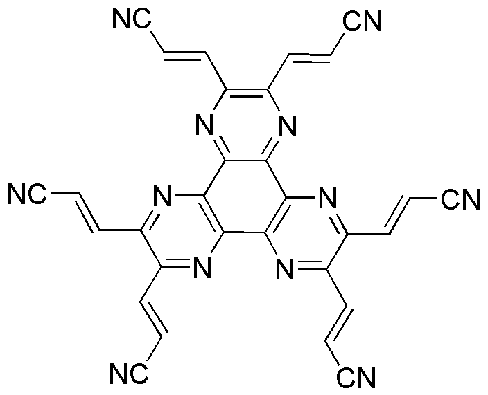
상기 제 1 전극의 도전층 상에 형성되는 n-형 유기물층은 하기의 화학식 1화합물을 포함한다.The n-type organic compound layer formed on the conductive layer of the first electrode includes the following Chemical Formula 1.
[화학식 1][Formula 1]

상기 화학식 1에 있어서, R1 내지 R6는 각각 수소, 할로겐 원자, 니트릴(-CN), 니트로(-NO2), 술포닐(-SO2R), 술폭사이드(-SOR), 술폰아미드(-SO2NR), 술포네이트(-SO3R), 트리플루오로메틸(-CF3), 에스테르(-COOR), 아미드(-CONHR 또는 -CONRR'), 치환 또는 비치환된 직쇄 또는 분지쇄의 C1-C12 알콕시, 치환 또는 비치환된 직쇄 또는 분지쇄 C1-C12의 알킬, 치환 또는 비치환된 방향족 또는 비방향족의 헤테로 고리, 치환 또는 비치환된 아릴, 치환 또는 비치환된 모노- 또는 디-아릴아민, 및 치환 또는 비치환된 아랄킬아민으로 구성된 군에서 선택되며, 상기 R 및 R'는 각각 치환 또는 비치환된 C1-C60의 알킬, 치환 또는 비치환된 아릴 및 치환 또는 비치환의 5-7원 헤테로 고리로 이루어진 군에서 선택된다. In Formula 1, R 1 to R 6 are each hydrogen, a halogen atom, nitrile (-CN), nitro (-NO 2 ), sulfonyl (-SO 2 R), sulfoxide (-SOR), sulfonamide ( -SO 2 NR), sulfonate (-SO 3 R), trifluoromethyl (-CF 3 ), ester (-COOR), amide (-CONHR or -CONRR '), substituted or unsubstituted straight or branched chain C 1 -C 12 alkoxy, substituted or unsubstituted straight or branched chain C 1 -C 12 alkyl, substituted or unsubstituted aromatic or non-aromatic hetero ring, substituted or unsubstituted aryl, substituted or unsubstituted Mono- or di-arylamine, and substituted or unsubstituted aralkylamine, wherein R and R 'are each substituted or unsubstituted C 1 -C 60 alkyl, substituted or unsubstituted aryl And it is selected from the group consisting of a substituted or unsubstituted 5-7 membered hetero ring.
상기 화학식 1의 화합물은 하기 화학식 1-1 내지 1-6의 화합물로 예시될 수 있다.The compound of Formula 1 may be exemplified by the compound of Formula 1-1 to 1-6.
[화학식 1-1][Formula 1-1]

[화학식 1-2][Formula 1-2]

[화학식 1-3][Formula 1-3]

[화학식 1-4][Formula 1-4]

[화학식 1-5][Formula 1-5]

[화학식 1-6][Formula 1-6]

또한 상기 n-형 유기물층은 2,3,5,6-테트라플루오로-7,7,8,8-테트라시아노퀴노디메탄(F4TCNQ), 불소-치환된 3,4,9,10-페릴렌테트라카르복실릭 디안하이드라이드(PTCDA), 시아노-치환된 3,4,9,10-페릴렌테트라카르복실릭 디안하이드라이드(PTCDA), 나프탈렌테트라카르복실릭디안하이드라이드(NTCDA), 불소-치환된 나프탈렌테트라카르복실릭디안하이드라이드(NTCDA), 시아노-치환된 나프탈렌테트라카르복실릭디안하이드라이드(NTCDA)를 포함한다.In addition, the n-type organic compound layer is 2,3,5,6-tetrafluoro-7,7,8,8-tetracyanoquinomethane (F4TCNQ), fluorine-substituted 3,4,9,10-pe Relenetetracarboxylic dianhydride (PTCDA), cyano-substituted 3,4,9,10-perylenetetracarboxylic dianhydride (PTCDA), naphthalenetetracarboxylic dianhydride (NTCDA), Fluorine-substituted naphthalenetetracarboxylic dianhydride (NTCDA), cyano-substituted naphthalenetetracarboxylic dianhydride (NTCDA).
본 발명의 예시적인 일 구현예에 따른 전기소자는 정공을 주입 또는 추출하는 제 1 전극의 n-형 유기물층을 접촉하는 p-형 유기물층을 포함한다. 따라서 상기 제 1 전극의 n-형 유기물층과 p-형 유기물층사이에 NP 접합이 형성된다. 도 2는 상기 제 1 전극의 n-형 유기물층과 p-형 유기물층의 사이에서 형성된 NP 접합을 나타낸다.An electric device according to an exemplary embodiment of the present invention includes a p-type organic compound layer contacting the n-type organic compound layer of the first electrode for injecting or extracting holes. Therefore, an NP junction is formed between the n-type organic compound layer and the p-type organic compound layer of the first electrode. 2 shows an NP junction formed between an n-type organic compound layer and a p-type organic compound layer of the first electrode.
NP 접합이 형성된 경우 제 1 전극의 n형 유기물층의 LUMO 준위와 p-형 유기물층의 HOMO 준위 사이의 에너지 준위 차이는 감소된다. 따라서 외부 전압이나 광 원에 의하여 정공 또는 전자가 용이하게 형성된다. p-형 유기물층 내에서 정공 또는 제 1 전극의 n-형 유기물층 내에서 전자도 NP 접합에 의하여 용이하게 형성된다. 상기 NP 접합에서 정공과 전자가 동시에 발생되므로, 전자는 제 1 전극의 n-형 유기물층을 통하여 제 1 전극의 도전층으로 수송되며 정공은 p-형 유기물층으로 수송된다.When the NP junction is formed, the difference in energy level between the LUMO level of the n-type organic compound layer of the first electrode and the HOMO level of the p-type organic compound layer is reduced. Therefore, holes or electrons are easily formed by an external voltage or a light source. Electrons in the p-type organic compound layer or in the n-type organic compound layer of the first electrode are also easily formed by NP bonding. Since holes and electrons are simultaneously generated at the NP junction, electrons are transported to the conductive layer of the first electrode through the n-type organic compound layer of the first electrode and holes are transported to the p-type organic compound layer.
본 발명의 예시적인 일 구현예의 전기소자는 이에 한정되지 않지만 유기 발광 소자, 유기 태양 전지 및 유기 트랜지스터를 포함한다.An electric device of an exemplary embodiment of the present invention includes, but is not limited to, an organic light emitting device, an organic solar cell, and an organic transistor.
유기 발광 소자Organic light emitting device
유기 발광 소자는 도전층 상에 n-형 유기물층으로 이루어진 애노드, 캐소드 및 상기 n-형 유기물층과 캐소드의 사이에 위치하며 상기 n-형 유기물층과 NP 접합을 형성하는 p-형 유기물층을 포함한다. 상기 p-형 유기물층과 캐소드 사이에는 정공주입층, 정공수송층, 발광층, 전자수송층 및 전자주입층으로부터 선택되는 하나 이상의 층을 포함한다. The organic light emitting device includes an anode, a cathode, and a p-type organic compound layer formed between the n-type organic compound layer and the cathode and forming an NP junction with the n-type organic compound layer on the conductive layer. The p-type organic material layer and the cathode include one or more layers selected from a hole injection layer, a hole transport layer, a light emitting layer, an electron transport layer and an electron injection layer.
도 3은 본 발명의 예시적인 일 구현예에 따른 유기 발광 소자를 나타낸다. 도 3을 참조하면, 본 발명에 따른 유기 발광 소자의 제 1 구현예 내지 제 3 구현예는 하기의 순서로 형성될 수 있다.3 illustrates an organic light emitting device according to an exemplary embodiment of the present invention. Referring to FIG. 3, the first to third embodiments of the organic light emitting diode according to the present invention may be formed in the following order.
제 1 First 구현예Embodiment
- 기판(31)
- 애노드(32) : 도전층(32a)/n-형 유기물층(32b)Anode 32:
- p-형 정공주입층(33)p-type hole injection layer (33)
- 정공수송층(34)-Hole transport layer (34)
- 발광층(35)
- 전자수송층(36)-Electron transport layer (36)
- 캐소드(37)-Cathode (37)
제 2 2nd 구현예Embodiment
- 기판(31)
- 애노드(32): 도전층(32a)/n-형 유기물층(32b)-Anode 32:
- p-형 정공수송층(34)p-type hole transport layer (34)
- 발광층(35)
- 전자수송층(36)-Electron transport layer (36)
- 캐소드(37)-Cathode (37)
제 3 3rd 구현예Embodiment
기판(31)
애노드(32): 도전층(32a)/n-형 유기물층(32b)Anode 32:
p-형 발광층(35)p-type light emitting layer (35)
전자수송층(36)Electron transport layer (36)
캐소드(37)Cathode (37)
상기 제 1 구현예 및 제2 구현예에 있어서 정공수송층(34), 발광층(35), 및 전자수송층(36)은 동일한 유기물질로 또는 다른 유기물질로 형성될 수 있으며, 상기 제 2 구현예의 경우 n-형 유기물층(32b)이 정공주입층의 역할을 동시에 하게 되며, 상기 제 3 구현예의 경우 n-형유기물층(32b)이 정공주입층과 정공수송층의 역할을 하게 된다.In the first and second embodiments, the
상기 제1 구현예 내지 제 3 구현예에서 n-형 유기물층(32b)의 LUMO 에너지 준위와 도전층(32a)의 페르미 에너지 준위의 에너지 차이는 2 내지 4eV이다. 제 1 구현예, 제 2 구현예 및 제 3 구현예에 있어서 n-형 유기물층(32b)과 NP 접합을 이루는 p-형 유기물층은 각각 p-형 정공주입층(33), p-형 정공수송층(34) 및 p-형 발광층(35)이 되며, 상기 NP 접합을 이루는 n-형 유기물층(32b)의 LUMO에너지 준위와 p-형 유기물층의 HOMO 에너지 준위의 에너지 차이는 약 1eV이하이며 바람직하게는 약 0.5eV 이하이다. In the first to third embodiments, the energy difference between the LUMO energy level of the n-type
n-형 유기물층(32b)의 LUMO 에너지 준위와 도전층(32a)의 페르미 에너지 준위의 에너지 차이가 4eV 보다 크면, p-형 정공주입층(33)으로의 정공 주입을 위한 에너지 장벽에 대한 표면쌍극자 또는 갭 스테이트의 효과가 감소한다. 상기 n-형 유기물층(32b)의 LUMO 에너지 준위와 상기 p-형 정공주입층(33)의 HOMO 에너지 준위의 에너지 차이가 약 1eV 보다 크면, p-형 정공주입층(33) 또는 n-형 유기물층(32b)에서 각각 정공 또는 전자가 용이하게 발생하지 않는다. 정공 주입을 위한 구 동전압이 상승한다.If the energy difference between the LUMO energy level of the n-type
도 4는 유기 발광 소자의 이상적인 에너지 준위를 나타낸다. 이 에너지 준위에서 애노드 및 캐소드로부터 각각 정공 및 전자를 주입하기 위한 에너지 손실이 최소화된다. 도 5는 본 발명의 예시적인 일 구현예에 따른 유기 발광 소자의 에너지준위를 나타낸다. 4 shows an ideal energy level of the organic light emitting device. At this energy level, energy losses for injecting holes and electrons from the anode and cathode, respectively, are minimized. 5 is a view illustrating an energy level of an organic light emitting diode according to an exemplary embodiment of the present invention.
도 5를 참조하면, 본 발명의 다른 예시적인 구현예에 따른 유기 발광 소자는 도전층 및 n-형 유기물층(도 3 참조)을 갖는 애노드, p-형 정공주입층(HIL), 정공수송층(HTL), 발광층(EML), 전자수송층(ETL) 및 캐소드를 포함한다. 상기 애노드의 n-형유기물층의 LUMO 에너지 준위와 상기 애노드의 도전층의 페르미 에너지 준위의 에너지 차이는 2 내지 4eV 이하이고 또한 상기 애노드의 n-형 유기물층의 LUMO 에너지 준위와 p-형 정공주입층의 HOMO 에너지 준위의 에너지 차이는 약 1eV 이하이다. 정공/전자주입 또는 추출을 위한 에너지 장벽이 상기 애노드의 n-형 유기물층에 의하여 낮아졌기 때문에, 상기 애노드의 n-형 유기물층의 LUMO 에너지 준위 및 상기 p-형 정공주입층의 HOMO 에너지 준위를 이용하여 정공은 애노드로부터 발광층으로 용이하게 수송된다.Referring to FIG. 5, an organic light emitting diode according to another exemplary embodiment of the present invention includes an anode having a conductive layer and an n-type organic compound layer (see FIG. 3), a p-type hole injection layer (HIL), and a hole transport layer (HTL). ), A light emitting layer (EML), an electron transport layer (ETL) and a cathode. The energy difference between the LUMO energy level of the n-type organic compound layer of the anode and the Fermi energy level of the conductive layer of the anode is 2 to 4 eV or less, and the LUMO energy level of the n-type organic compound layer of the anode and the p-type hole injection layer The energy difference of HOMO energy levels is about 1 eV or less. Since the energy barrier for hole / electron injection or extraction is lowered by the n-type organic compound layer of the anode, the LUMO energy level of the n-type organic compound layer of the anode and the HOMO energy level of the p-type hole injection layer Holes are easily transported from the anode to the light emitting layer.
상기 애노드의 n-형 유기물층이 애노드로부터 p-형 정공주입층, p-형 정공수송층 또는 p-형 발광층으로의 정공 주입을 위한 에너지 장벽을 낮추므로, 상기 애노드의 도전층은 다양한 도전성 물질로 형성될 수 있다. 예를 들면, 상기 도전층은 캐소드와 동일한 낮은 일함수를 갖는 물질인 Ca, Ca-Ag, Ca-IZO, Ma-Ag 등으로 형성될 수 있다. 애노드가 캐소드와 동일한 물질로 형성된 경우, 도전성 물질이 낮은 일함수를 갖는 스택형 유기 발광 소자와 같은 것이 제조될 수 있다.Since the n-type organic compound layer of the anode lowers the energy barrier for hole injection from the anode to the p-type hole injection layer, the p-type hole transport layer, or the p-type light emitting layer, the anode conductive layer is formed of various conductive materials. Can be. For example, the conductive layer may be formed of Ca, Ca-Ag, Ca-IZO, Ma-Ag, or the like, which has the same low work function as the cathode. When the anode is formed of the same material as the cathode, one such as a stacked organic light emitting device in which the conductive material has a low work function can be manufactured.
이처럼 캐소드 및 애노드가 동일한 재료로 형성될 수 있으므로 도 8에 나타낸 것과 같이 애노드(71)와 캐소드(75)의 사이에 개재된 유기물층(73)을 포함하는 단위 유기발광소자가 2 개 이상 직렬로 연결된 구조와 등가 구조를 갖는 도 9에 도시된 것과 같은 스택형 유기발광소자를 얻을 수 있다. 애노드(71)는 도전층과 n-형 유기물층을 포함한다.Since the cathode and the anode may be formed of the same material as described above, two or more unit organic light emitting devices including the
도 9를 참조하면, 본 발명에 따른 스택형 유기발광소자는 단위 유기 발광 소자의 캐소드의 도전층이 이웃한 단위 유기 발광 소자의 애노드로서 적층된 것으로서 애노드(81)와 캐소드(87) 사이에 유기물층(83)과 단위 유기 발광 소자의 캐소드의 도전층과 이웃한 단위 유기 발광 소자의 애노드로 작용하는 중간도전층(85)의 반복단위가 복수개 적층된 구조를 갖는다. 상기 도전층은 일함수가 캐소드(87) 물질의 그것과 비슷한 값을 가지면서 가시광선 투과율이 50% 이상인 투명한 물질로 형성되는 것이 바람직하다. 불투명 금속이 도전층으로 이용되는 경우, 도전층의 두께는 투명하게 될 정도로 얇게 형성되어야 한다. 불투명 금속의 구체적인 예로서는 Al, Ag, Cu, Ca, Ca-Ag 등을 들 수 있다. 낮은 일함수를 갖는 Ca를 중간도전층(85)의 도전층을 형성할 수 있으며, 특히 Ca-IZO를 채용하는 경우 가시광선 투과도를 개선할 수 있고, 스택형 유기 발광 소자의 경우 동일한 구동 전압 하에서 스택된 유기 발광 소자 단위의 수에 비례하여 휘도가 증가하므로 유기 발광 소자를 스택형으로 하면 고휘도 유기 발광 소자를 얻을 수 있다.Referring to FIG. 9, in the stacked organic light emitting diode according to the present invention, a conductive layer of a cathode of a unit organic light emitting diode is stacked as an anode of a neighboring unit organic light emitting diode, and an organic material layer is formed between the
이하, 본 발명의 예시적인 일 구현예에 따른 유기 발광 소자를 구성하는 각층에 대하여 구체적으로 설명한다. 이하에서 설명하는 각 층의 물질들은 단일 물질 또는 2 이상의 물질의 혼합물일 수 있다.Hereinafter, each layer constituting the organic light emitting device according to the exemplary embodiment of the present invention will be described in detail. The materials of each layer described below may be a single material or a mixture of two or more materials.
애노드Anode (Anode)(Anode)
애노드는 정공주입층, 정공수송층 또는 발광층과 같은 p-형 유기물층 내에 정공을 주입한다. 상기 애노드는 도전층과 n-형 유기물층을 포함한다. 상기 도전층은 금속, 금속 산화물 또는 도전성 폴리머를 포함한다. 상기 도전성 폴리머는 전기전도성 폴리머를 포함할 수 있다.The anode injects holes into a p-type organic compound layer, such as a hole injection layer, a hole transport layer or a light emitting layer. The anode includes a conductive layer and an n-type organic compound layer. The conductive layer comprises a metal, a metal oxide or a conductive polymer. The conductive polymer may include an electrically conductive polymer.
상기 n-형 유기물층은 p-형 유기물층에 정공주입을 위한 에너지 장벽을 낮추기 때문에, 상기 도전층은 다양한 도전성 물질로 형성될 수 있다. 예를 들면, 상기 도전층은 약 2.5 내지 5.5eV의 페르미 에너지 준위를 갖는다. 예시적인 도전성 물질의 예는 탄소, 알루미늄, 칼슘, 바나듐, 크롬, 구리, 아연, 은, 금, 기타 금속 및 이들의 합금; 아연 산화물, 인듐 산화물, 주석 산화물, 인듐 주석 산화물(ITO), 인듐 아연 산화물(IZO) 및 기타 이와 유사한 금속 산화물; Ca-Ag 및 Ca-IZO와 같은 금속-금속산화물 적층체 등이 있다. 유기 발광 소자가 전면발광형(top emission)인 경우에는 상기 도전층으로서 투명 물질 뿐만 아니라 광반사율이 우수한 불투명 물질도 사용될 수 있다. 후면발광형(bottom emission) 유기 발광 소자의 경우에는 상기 도전층으로서 투명 물질이어야 하며, 만일 불투명 물질이 사용되는 경우에는 투명하게 될 정도로 박막으로 형성되어야 한다.Since the n-type organic compound layer lowers the energy barrier for hole injection into the p-type organic compound layer, the conductive layer may be formed of various conductive materials. For example, the conductive layer has a Fermi energy level of about 2.5 to 5.5 eV. Examples of exemplary conductive materials include carbon, aluminum, calcium, vanadium, chromium, copper, zinc, silver, gold, other metals and alloys thereof; Zinc oxide, indium oxide, tin oxide, indium tin oxide (ITO), indium zinc oxide (IZO) and other similar metal oxides; Metal-metal oxide laminates such as Ca-Ag and Ca-IZO. When the organic light emitting device is a top emission type, not only a transparent material but also an opaque material having excellent light reflectance may be used as the conductive layer. In the case of a bottom emission organic light emitting device, the conductive layer should be a transparent material, and if an opaque material is used, it should be formed into a thin film so as to be transparent.
n-형 유기물층은 상기 도전층과 p-형 유기물층의 사이에 위치하며, 저전계 에서 정공을 p-형 유기물층으로 주입하게 되며, n-형 유기물층은 상기 애노드의 n-형 유기물층의 LUMO 에너지 준위와 상기 애노드의 도전층의 페르미 에너지 준위의 에너지 차이가 2eV 내지 4eV이고, 상기 n-형 유기물층의 LUMO 에너지 준위와 상기 p-형 유기물층의 HOMO 에너지 준위의 에너지 차이가 약 1eV 이하가 되도록 선택된다. 예를 들면, 상기 n-형 유기물층은 약 4 내지 7eV의 LUMO 에너지 준위 및 약 10-8cm2/Vs 내지 1 cm2/Vs, 바람직하게는 약 10-6cm2/Vs 내지 10-2cm2/Vs의 전자이동도를 갖는다. 전자이동도가 약 10-8cm2/Vs 미만이면 n-형 유기물층으로부터 p-형 유기물층으로 정공을 주입하기 쉽지 않다. 전자이동도가 1 cm2/Vs를 초과하면 정공주입이 더욱 효율적이 되지만 이와 같은 물질은 통상적으로 결정성 유기물이므로 비결정성 유기물을 이용하는 유기 발광 소자에 적용하기 어렵다.The n-type organic compound layer is positioned between the conductive layer and the p-type organic compound layer, and holes are injected into the p-type organic compound layer at a low electric field, and the n-type organic compound layer is formed in accordance with the LUMO energy level of the n-type organic compound layer of the anode. The energy difference of the Fermi energy level of the anode conductive layer is 2eV to 4eV, and the energy difference between the LUMO energy level of the n-type organic compound layer and the HOMO energy level of the p-type organic compound layer is selected to be about 1eV or less. For example, the n-type organic compound layer has a LUMO energy level of about 4 to 7 eV and about 10 -8 cm 2 / Vs to 1 cm 2 / Vs, preferably about 10 -6 cm 2 / Vs to 10 -2 cm It has an electron mobility of 2 / Vs. If the electron mobility is less than about 10 −8 cm 2 / Vs, holes may not be easily injected from the n-type organic compound layer to the p-type organic compound layer. If the electron mobility exceeds 1 cm 2 / Vs, the hole injection becomes more efficient, but such a material is typically a crystalline organic material, so it is difficult to apply to an organic light emitting device using an amorphous organic material.
상기 n-형 유기물층은 진공증착될 수 있는 물질 또는 솔루션 프로세스(solution process)로 박막 성형될 수 있는 물질로 형성될 수도 있다. 상기 n-형 유기물의 구체적인 예는 이에 한정되지 않지만 앞서 언급한 물질을 포함한다.The n-type organic compound layer may be formed of a material that can be vacuum deposited or a material that can be thin-film formed by a solution process. Specific examples of the n-type organic material include, but are not limited to, the aforementioned materials.
정공주입층Hole injection layer (( HILHIL ) 또는 정공수송층() Or hole transport layer ( HTLHTL ))
정공주입층 또는 정공수송층은 애노드와 캐소드의 사이에 위치하여 p-형 유기물층으로서 애노드의 도전층 상에 형성된 n-형 유기물층과 NP 접합을 형성하며, NP 접합에서 형성된 정공은 상기 p-형 정공주입층 또는 p-형 정공수송층을 통하여 발광층으로 수송된다.The hole injection layer or the hole transport layer is positioned between the anode and the cathode to form an NP junction with the n-type organic compound layer formed on the conductive layer of the anode as a p-type organic compound layer, and the holes formed in the NP junction are the p-type hole injection. It is transported to the light emitting layer through the layer or the p-type hole transport layer.
상기 NP 접합을 하는 p-형 정공주입층 또는 p-형 정공수송층의 HOMO 에너지 준위는 예를 들면 상기 n-형 유기물층의 LUMO 에너지 준위에 대하여 약 1eV 이하의 에너지 차이, 바람직하게는 약 0.5eV의 에너지 차이를 갖는다. 상기 p-형 정공주입층 또는 p-형 정공수송층은 아릴아민계 화합물, 도전성 폴리머, 또는 공역 부분과 비공역 부분이 함께 있는 블록 공중합체 등을 포함하지만, 이에 한정되는 것은 아니다.The HOMO energy level of the p-type hole injection layer or the p-type hole transport layer which is the NP junction is, for example, an energy difference of about 1 eV or less with respect to the LUMO energy level of the n-type organic compound layer, preferably about 0.5 eV. Has an energy difference. The p-type hole injection layer or the p-type hole transport layer may include, but is not limited to, an arylamine-based compound, a conductive polymer, or a block copolymer having a conjugated portion and a non-conjugated portion.
발광층(Light emitting layer EMLEML ))
발광층에서는 정공전달과 전자전달이 동시에 일어나므로 발광층은 n-형 특성과 p-형 특성을 모두 가질 수 있다. 편의상 전자 수송이 정공 수송에 비하여 빠를 경우 n-형 발광층, 정공 수송이 전자 수송에 비하여 빠를 경우 p-형 발광층이라고 정의할 수 있다.In the light emitting layer, since hole and electron transfer occur at the same time, the light emitting layer may have both n-type and p-type characteristics. For convenience, the electron transport may be defined as an n-type light emitting layer faster than the hole transport, and the hole transport may be defined as a p-type light emitting layer faster than the electron transport.
n-형 발광층에서는 전자수송이 정공수송 보다 빠르기 때문에 정공수송층과 발광층의 계면 부근에서 발광이 이루어지므로 정공수송층의 LUMO준위가 발광층의 LUMO 준위보다 높으면 더 좋은 발광효율을 나타낼 수 있다. n-형 발광층은 이에 한정되지 않지만 알루미늄 트리스(8-히드록시퀴놀린)(Alq3); 8-히드록시퀴놀린베릴륨(BAlq); 벤즈옥사졸계 화합물, 벤즈티아졸계 화합물 또는 벤즈이미다졸계 화합물; 폴리플루오렌계 화합물; 실라사이클로펜타디엔(silole)계 화합물 등을 포함한다.Since the electron transport is faster than the hole transport in the n-type light emitting layer, light emission occurs near the interface between the hole transport layer and the light emitting layer. Therefore, when the LUMO level of the hole transport layer is higher than the LUMO level of the light emitting layer, the light emission efficiency may be better. The n-type light emitting layer includes, but is not limited to, aluminum tris (8-hydroxyquinoline) (Alq 3 ); 8-hydroxyquinolineberyllium (BAlq); Benzoxazole compound, benzthiazole compound or benzimidazole compound; Polyfluorene-based compounds; Silacyclopentadiene (silole) compounds and the like.
p-형 발광층에서는 정공수송이 전자수송 보다 빠르기 때문에 전자수송층과 발광층의 계면 부근에서 발광이 이루어지므로 전자수송층의 HOMO 준위가 발광층의 HOMO 준위보다 낮으면 더욱 좋은 발광 효율을 나타낼 수 있다. p-형 발광층을 사용하는 경우, 정공수송층의 LUMO 준위 변화에 의한 발광효율의 증대효과가 n-형 발광층을 사용하는 경우에 비하여 작기 때문에 p-형 발광층을 사용하는 경우에는 정공주입층과 정공수송층을 사용하지 않고 n-형 유기물층과 p-형 발광층 사이의 NP 접합구조를 가지는 유기 발광 소자를 제조할 수 있다. p-형 발광층은 이에 한정되는 것은 아니지만 카바졸계 화합물; 안트라센계 화합물; 폴리페닐렌비닐렌(PPV)계 폴리머; 또는 스피로(spiro) 화합물 등을 포함한다.In the p-type light emitting layer, since the hole transport is faster than the electron transport, light is emitted near the interface between the electron transport layer and the light emitting layer, and thus, when the HOMO level of the electron transport layer is lower than the HOMO level of the light emitting layer, the light emission efficiency may be better. In the case of using the p-type light emitting layer, since the effect of increasing the luminous efficiency due to the change in the LUMO level of the hole transport layer is smaller than in the case of using the n-type light emitting layer, the hole injection layer and the hole transport layer are used in the case of using the p-type light emitting layer. An organic light emitting device having an NP junction structure between an n-type organic compound layer and a p-type light emitting layer may be manufactured without using a. The p-type light emitting layer is not limited thereto, but includes a carbazole compound; Anthracene-based compounds; Polyphenylenevinylene (PPV) -based polymers; Or spiro compounds and the like.
전자수송층(Electron transport layer ETLETL ))
전자수송층 물질로서는 캐소드로부터 전자를 효과적으로 주입받아 발광층으로 잘 수송할 수 있도록 전자이동도(electron mobility)가 큰 물질이 바람직하다. 상기 전자수송층은 이에 한정되지 않지만 알루미늄 트리스(8-히드록시퀴놀린)(Alq3); Alq3구조를 포함하는 유기화합물; 히드록시플라본-금속 착화합물 또는 실라사이클로펜타디엔(silole)계 화합물 등을 포함한다.As the electron transport layer material, a material having a high electron mobility is preferably used to effectively inject electrons from the cathode and transport the electrons to the light emitting layer. The electron transport layer is not limited thereto, but may include aluminum tris (8-hydroxyquinoline) (Alq 3 ); Organic compounds containing Alq 3 structures; Hydroxyflavone-metal complex compounds or silacyclopentadiene (silole) compounds.
캐소드Cathode (Cathode)(Cathode)
캐소드 물질로는 통상 전자수송층과 같은 n-형 유기물층의 LUMO 준위로 전자 주입이 용이하게 이루어지도록 일함수가 작은 물질이 바람직하다. 상기 캐소드는 이에 한정되지 않지만 마그네슘, 칼슘, 나트륨, 칼륨, 티타늄, 인듐, 이트륨, 리튬, 가돌리늄, 알루미늄, 은, 주석 및 납과 같은 금속 또는 이들의 합금; LiF/Al또는 LiO2/Al과 같은 다층 구조 물질 등을 포함한다. 상기 캐소드는 애노드의 도전층과 동일한 물질로 형성될 수 있으며, 또한 캐소드 또는 애노드의 도전층은 투명 물질을 포함할 수 있다.As the cathode material, a material having a small work function is generally preferred so that electron injection is easily performed at an LUMO level of an n-type organic compound layer such as an electron transport layer. The cathode is, but is not limited to, metals such as magnesium, calcium, sodium, potassium, titanium, indium, yttrium, lithium, gadolinium, aluminum, silver, tin and lead or alloys thereof; Multilayer structure materials such as LiF / Al or LiO 2 / Al, and the like. The cathode may be formed of the same material as the conductive layer of the anode, and the cathode or the conductive layer of the anode may include a transparent material.
유기 태양전지Organic solar cell
유기 태양전지는 애노드, 캐소드, 및 상기 애노드와 상기 캐소드의 사이에 개재된 유기박막을 포함한다. 상기 유기 박막은 유기 태양전지의 효율과 안정성을 높이기 위하여 복수개의 층을 포함한다. 도 6을 참조하면 본 발명에 따른 유기태양전지의 예시적인 일 구현예는 다음의 순서로 형성될 수 있다.The organic solar cell includes an anode, a cathode, and an organic thin film interposed between the anode and the cathode. The organic thin film includes a plurality of layers in order to increase efficiency and stability of the organic solar cell. Referring to FIG. 6, an exemplary embodiment of the organic solar cell according to the present invention may be formed in the following order.
- 기판(41)
- 애노드(42): 도전층(42a)/n-형 유기물층(42b)Anode 42:
- 전자 도너층(electron donor layer; 43)An
- 전자 억셉터층(electron acceptor; 44)An
- 캐소드(45)-Cathode (45)
유기 태양전지가 외부 광원으로부터 광자를 받으면 전자 도너층(43)과 전자 억셉터층(44) 사이에서 전자와 정공이 발생하게 되며, 발생된 정공은 전자 도너층(43)을 통하여 애노드(42)로 수송된다. 상기 도너층(43)은 상기 n-형 유기물층과 NP접합을 이루는 p-형 유기물로서 형성되며, 상기 p-형 유기물층은 2종 이상의 물질의 조합일 수 있다. 본 발명의 다른 예시적인 구현예에 따른 유기 태양전지는 부가적인 유기박막을 더 포함하거나 제조 단계를 간단히 하기 위하여 특정 유기 박막을 생략할 수 있다. 상기 유기 태양전지는 여러 가지 기능을 동시에 갖는 유기물을 사용하여 유기물층의 수를 감소시킬 수 있다.When the organic solar cell receives photons from an external light source, electrons and holes are generated between the
종래의 유기 태양전지는 전자 도너층과 같은 유기 박막의 HOMO 에너지 준위를 따라 정공을 애노드로 수송하기 때문에 애노드의 페르미 에너지 준위와 전자 도너층의 HOMO 에너지 준위의 에너지 준위 차이가 작을수록 정공추출이 더 많이 일어난다. 그러나 본 발명의 예시적인 일 구현예에 따른 유기 태양전지는 n-형 유기물층(42b)과 전자 도너층(43)의 사이에서 NP 접합이 형성됨으로서 정공이 효율적으로 추출되며, 추출된 정공은 n-형 유기물층(42b)의 LUMO 에너지 준위를 통하여 도전층(42a)으로 주입된다.In the conventional organic solar cell, holes are transported to the anode along the HOMO energy level of the organic thin film such as the electron donor layer, so that the smaller the difference between the Fermi energy level of the anode and the HOMO energy level of the electron donor layer, the more hole extraction is achieved. A lot happens. However, in the organic solar cell according to the exemplary embodiment of the present invention, holes are efficiently extracted by forming an NP junction between the n-type
n-형 유기물층(42b)의 LUMO 에너지 준위와 도전층(42a)의 페르미 준위의 에너지 차이는 2 eV 내지 4eV이고, n-형 유기물층(42b)의 LUMO 에너지 준위와 전자 도너층(43)과 같은 p-형 유기물층(44)의 HOMO 준위의 차이는 약 1 eV 이하이다. 도전층(42a)은 다양한 페르미 에너지 준위를 갖는 물질로 형성될 수 있으며, 캐소드(45)와 애노드(42)는 동일한 물질로 형성될 수 있다.The energy difference between the LUMO energy level of the n-type
상기 유기 태양전지의 도전층(42a) 및 캐소드(45)는 상기 유기 발광 소자의 도전층 및 캐소드 물질로 형성될 수 있다. 또한 상기 유기 태양전지의 n-형 유기물층은 상기 유기 발광 소자에서의 n-형 유기물층으로 형성될 수 있다. 상기 유기 태양전지에서 전자 억셉터층(44)은 상기 유기 발광 소자에서의 전자수송층 물질 또는 n-형 발광층 물질 또는 풀러렌(fullerene)계 화합물로서 개시된 것으로 형성될 수 있다. 상기 유기 태양전지에서 전자 도너층(43)은 상기 유기 발광 소자에서의 p-형 정공수송층 물질 또는 p-형 발광층 물질 또는 티오펜계 폴리머로 형성될 수 있다.The
유기 트랜지스터Organic transistor
도 7을 참조하면 본 발명의 예시적인 일 구현예에 따른 유기 트랜지스터를 나타낸다.Referring to FIG. 7, an organic transistor according to an exemplary embodiment of the present invention is shown.
도 7을 참조하면, 유기 트랜지스터는 기판(61), 소스 전극(65), 드레인 전극(66),게이트(62), 기판(61)과 게이트(52) 위에 위치하는 절연층(63), 절연층(63)상에 위치하며 정공을 형성하는 p-형 유기물층(64), 소스 전극(65) 및/또는 드레인 전극(66)과 p-형 유기물층(64)의 사이에 위치하는 n-형 유기물층(67)을 포함한다. n-형유기물층(67)의 LUMO 에너지 준위와 소스 전극(65) 또는 드레인 전극(66)의 페르미에너지 준위의 에너지 차이는 2 eV 내지 4eV이다. n-형 유기물층(67)의 LUMO 에너지준위와 p-형 유기물층(64)의 HOMO 에너지 준위의 에너지 차이는 약 1 eV 이하이다.Referring to FIG. 7, the organic transistor includes a
n-형 유기물층(67)은 LUMO 준위를 통하여 정공을 소스 전극(65)으로부터 추 출하여 이를 드레인 전극(66)으로 주입할 수 있다. n-형 유기물층(67)과 p-형 유기물층(64)의 사이에 NP 접합이 형성되기 때문에, 정공이 소스 전극(65)과 드레인 전극(66)의 사이에서 원활하게 수송될 수 있다. 본 발명의 다른 예시적인 구현예에서 n-형 유기물층(67)은 소스 전극(65) 또는 드레인 전극(66)의 일부분을 형성할 수 있으며, 이 경우에는 다양한 페르미 에너지 준위를 갖는 물질이 소스 전극(65)과 드레인 전극(66)을 형성할 수 있다.The n-type
본 발명의 예시적인 일 구현예의 유기 트랜지스터에서 n-형 유기물층(67)은 상기 유기 발광 소자의 n-형 유기물층용 물질로 형성될 수 있다. 게이트(62)로서는 상기 유기 발광 소자의 애노드 또는 캐소드 물질로서 예시된 물질로 형성될 수 있다.In the organic transistor of the exemplary embodiment of the present invention, the n-type
소스 전극(65) 또는 드레인 전극(66)은 상기 유기 발광 소자의 애노드 물질로서 예시된 물질로 형성될 수 있다. p-형 유기물층(64)은 이에 한정되지 않지만 펜타센(pentacene)계 화합물, 안트라디티오펜(antradithiophene)계 화합물, 벤조디티오펜(benzodithiophene)계 화합물, 티오펜계 올리고머류(thiophene oligomers), 폴리티오펜류(polythiophenes), 혼합된 서브유닛 티오펜 올리고머류(mixed-subunitthiophene oligomers), 옥시-관능화된 티오펜 올리고머류(oxy-funcionalized thiophene oligomers) 등으로 형성될 수 있다. 절연층(63)은 산화실리콘(silicon oxide), 질화실리콘(silicon nitride); 폴리이미드, 폴리(2-비닐피리딘), 폴리(4-비닐페놀), 또는 폴리(메틸메타크릴레이트)와 같은 폴리머로 형성될 수 있다.The source electrode 65 or the
이하, 실시예를 통하여 본 발명의 다양한 태양 및 특징을 더욱 상세히 설명한다. 그러나, 하기 실시예는 본 발명의 다양한 태양 및 특징을 예시하기위한 것에 불과하며, 본 발명의 범위가 하기 실시예에 의하여 한정되는 것은 아니다. Hereinafter, various aspects and features of the present invention will be described in more detail with reference to Examples. However, the following examples are only intended to illustrate various aspects and features of the present invention, and the scope of the present invention is not limited by the following examples.
[실시예]EXAMPLE
UPS 및 UV-VIS 흡수(absorption) 방법에 의한 헥사니트릴 헥사아자트리페닐렌(화학식 1-1, HAT, 한국공개특허 제2003-67773호 참조)의 HOMO와 LUMO준위는 PCT/KR2005/001381호에 기재된 방법에 의하여 측정하였으며, 측정된 HAT의 HOMO 준위는 9.78eV 이었으며, HAT의 LUMO는 약 6.54eV이었다. 이 값은 HAT 물질의 엑시톤 결합에너지(exciton binding energy)에 의해서 변화될 수 있다. 즉, 6.54eV는 상기 물질의 페르미 준위(6.02eV) 보다 큰 값으로 LUMO 준위가 페르미 준위보다 더 작은 값을 갖기 위하여서는 엑시톤 결합에너지가 0.52eV 이상이어야 하는 것을 알 수 있다. 유기물의 엑시톤 결합에너지는 통상 0.5eV 내지 1eV의 값을 가지므로 상기 HAT의 LUMO 준위는 5.54 내지 6.02eV의 값을 가질 것으로 예측되었다.HOMO and LUMO levels of hexanitrile hexaazatriphenylene (see Formula 1-1, HAT, Korean Patent Publication No. 2003-67773) by UPS and UV-VIS absorption method are described in PCT / KR2005 / 001381. It was measured by the method described, the measured HOMO level of the HAT was 9.78eV, LUMO of the HAT was about 6.54eV. This value can be changed by the exciton binding energy of the HAT material. That is, 6.54 eV is greater than the Fermi level (6.02 eV) of the material, it can be seen that the exciton binding energy should be 0.52 eV or more in order to have a LUMO level smaller than the Fermi level. Since the exciton binding energy of the organic material usually has a value of 0.5 eV to 1 eV, the LUMO level of the HAT was expected to have a value of 5.54 to 6.02 eV.
유리 기판(Corning 7059glass)은 세제(제조사: Fischer Co., 제품번호: 15-335-55)가 용해된 증류수에 넣고 초음파로 30 분간 세정한 후, 증류수에 넣고 5분간 실시하는 초음파 세정을 2회 반복하고, 이소프로필알콜, 아세톤, 및 메탄올 용제에서 상기 유리기판을 이 순서로 각 1회씩 초음파 세정을 실시하고 건조시킨 후, 사용하였다. The glass substrate (Corning 7059glass) is placed in distilled water in which detergent (manufacturer: Fischer Co., product number: 15-335-55) is dissolved in ultrasonic water for 30 minutes, and then ultrasonically cleaned in distilled water for 5 minutes. The glass substrates were repeatedly subjected to ultrasonic cleaning in this order once in an isopropyl alcohol, acetone, and methanol solvent, dried, and then used.
[실시예 1] Example 1
IZOIZO -Ca -Ca 도전층Conductive layer 및 HAT n-형 유기물층을 구비한 And a HAT n-type organic compound layer 애노드를Anode 포함하는 유기 발광 소자 Organic light emitting device comprising
세정된 유리기판위에 인듐 아연 산화물(IZO)를 1000Å의 두께로 스퍼터링 증착기를 사용하여 진공 증착하고 그 위에 100Å 두께로 Ca를 진공 열증착하여 일함수가 2.6eV인 투명 IZO-Ca 도전층을 형성하였다. 상기 형성된 도전층 상에 약 500Å 두께의 HAT를 열진공증착하여 IZO-Ca 도전층 및 HAT n-형 유기물층을 갖는 투명 애노드를 형성하였다. 이어서 약 400Å 두께로 4,4'-비스[N-(1-나프틸)-N-페닐아미노]비페닐(NPB)을 진공 증착하여 p-형 정공수송층을 형성하였다. 상기 p-형 정공수송층 상에 HOMO 준위가 약 5.7eV인 Alq3를 약 300Å 두께로 진공증착하여 발광층을 형성시키고, 상기 발광층 상에 하기 화합물(HOMO 준위 = 약 5.7eV)을 200Å 두께로 진공증착 하여 전자수송층을 형성시켰다.Indium zinc oxide (IZO) was vacuum deposited on the cleaned glass substrate using a sputtering evaporator at a thickness of 1000 kV, and Ca was vacuum-heat-deposited at 100 kW thereon to form a transparent IZO-Ca conductive layer having a work function of 2.6 eV. . About 500 kW thick HAT was thermally vacuum deposited on the formed conductive layer to form a transparent anode having an IZO-Ca conductive layer and a HAT n-type organic compound layer. Subsequently, 4,4'-bis [N- (1-naphthyl) -N-phenylamino] biphenyl (NPB) was vacuum deposited to a thickness of about 400 mm 3 to form a p-type hole transport layer. Alq3 having a HOMO level of about 5.7 eV was vacuum deposited on the p-type hole transport layer to a thickness of about 300 kV to form a light emitting layer, and the following compound (HOMO level = about 5.7 eV) was vacuum deposited to 200 kW on the light emitting layer. An electron transport layer was formed.

상기 전자수송층 위에 12Å 두께의 리튬 플루오라이드(LiF) 박막과 2500Å두 께의 알루미늄을 진공증착하여 캐소드를 형성함으로써 유기 발광 소자를 완성하였다. 상기 과정에서 유기물의 증착속도는 약 0.4~0.7Å/sec를 유지하였고, LiF는 약 0.3Å/sec, 칼슘 및 알루미늄은 약 2Å/sec의 증착속도를 유지하였다. 증착 시 증착 챔버 내의 진공도는 약 2X10⁻⁷ 내지 5X10⁻⁸ torr를 유지하였다.An organic light-emitting device was completed by forming a cathode by vacuum depositing a lithium fluoride (LiF) thin film having a thickness of 12 kHz and aluminum having a thickness of 2500 kHz on the electron transport layer. In the process, the deposition rate of the organic material was maintained at about 0.4 ~ 0.7 Å / sec, LiF was about 0.3 Å / sec, calcium and aluminum was maintained at a deposition rate of about 2 Å / sec. The degree of vacuum in the deposition chamber during deposition was maintained at about 2 × 10 −7 to 5 × 10 −8 torr.
[실시예 2]Example 2
AgAg -Ca -Ca 도전층Conductive layer 및 HAT n-형 유기물층을 구비한 And a HAT n-type organic compound layer 애노드를Anode 포함하는 유기 발광 소자 Organic light emitting device comprising
세정된 유리기판위에 IZO-Ca 투명 도전층 대신 Ag를 200Å의 두께로 진공 열증착하고 그 위에 200Å 두께로 Ca를 진공 열증착하여 일함수가 2.6eV인 반투명 Ag-Ca 도전층을 형성한 것 이외에는 실시예 1과 동일한 방법으로 유기 발광 소자를 제작하였다.Except for forming a semi-transparent Ag-Ca conductive layer having a work function of 2.6 eV by vacuum thermal evaporation of Ag to 200 μs on the cleaned glass substrate and vacuum thermal evaporation of Ca to 200 μs on it instead of the IZO-Ca transparent conductive layer. An organic light emitting device was manufactured in the same manner as in Example 1.
[표 1]TABLE 1

상기 실시예 1 및 실시예 2의 전류 밀도 및 전압에 따른 휘도를 나타내는 표 1의 결과로부터 n-형 유기물층의 LUMO 에너지 준위가 약 5.54 내지 약 6.02 eV인 HAT와 도전층의 일함수(2.6eV)의 에너지 차이가 2.9 내지 3. 4 정도임에도 불구하고 정공수송층으로 정공이 원활하게 주입됨을 알 수 있고, 이는 n-형 유기물층의 LUMO 에너지 준위와 상기 도전층의 일함수의 에너지 차이가 2 내지 4eV인 범위에서 유기 발광 소자의 전류-전압 특성은 도전층의 일함수 값에 독립적인 것을 의미한다.The work function of the HAT and the conductive layer (2.6 eV) in which the LUMO energy level of the n-type organic compound layer is about 5.54 to about 6.02 eV from the results of Table 1 showing the luminance according to the current density and voltage of Examples 1 and 2 above. It can be seen that the hole is smoothly injected into the hole transport layer even though the energy difference is about 2.9 to 3. 4, which means that the energy difference between the LUMO energy level of the n-type organic compound layer and the work function of the conductive layer is 2 to 4 eV. In the range, the current-voltage characteristic of the organic light emitting diode is meant to be independent of the work function value of the conductive layer.
한편 실시예 2에 따른 유기 발광 소자의 휘도가 실시예 1에 따른 유기 발광 소자의 휘도에 비하여 상대적으로 낮은 것은 Ag(200Å)-Ca(200Å) 도전층이 IZO(1000Å)-Ca(100Å) 도전층에 비하여 가시광선 투과도가 현저히 떨어지는 것에 기인된 것으로서 실시예 2의 유기 발광 소자의 휘도는 상기 가시광 투과도를 감안할 때 실시예 1의 도전층을 갖는 소자의 그것과 동등한 것으로 판단된다.On the other hand, the luminance of the organic light emitting diode according to Example 2 is relatively lower than that of the organic light emitting diode according to Example 1 in that the Ag (200 Å) -Ca (200 Å) conductive layer is IZO (1000 Å) -Ca (100 Å) conductive. The luminance of the organic light-emitting device of Example 2 is considerably lower than that of the device having the conductive layer of Example 1 in view of the visible light transmittance due to the remarkably inferior visible light transmittance compared to the layer.
상기의 결과들은 캐소드 전극으로 사용되는 낮은 페르미 에너지를 갖는 칼슘 등을 도전층으로 하며 상기 도전층의 페르미 에너지 준위의 에너지 차이가 2 내지 4 eV의 범위이고, 상기 n-형 유기물층과 상기 p-형 유기물층의 사이에서 NP접합을 형성하는 p-형 유기물층의 HOMO 에너지 준위와 n-형 유기물층의 LUMO 에너지 준위의 차이가 1 eV 이하의 조건일 때 애노드로 채용 가능하다는 것을 보여주는 것이며, 이는 애노드의 도전층과 캐소드를 동일한 물질을 사용하는 것을 의미하고, 이를 이용하여 도 9에 도시된 스택형 유기발광 소자를 구현할 수 있음을 의미한다.The above results are based on calcium having low Fermi energy used as the cathode electrode and the like, and the energy difference of the Fermi energy level of the conductive layer is in the range of 2 to 4 eV, and the n-type organic compound layer and the p-type This shows that the difference between the HOMO energy level of the p-type organic compound layer forming the NP junction and the LUMO energy level of the n-type organic compound layer between the organic layer is 1 eV or less, which can be used as the anode, which is the conductive layer of the anode This means using the same material as the cathode, it means that can be implemented using the stacked organic light emitting device shown in FIG.
상기한 바와 같이, 본 발명에 따른 전기 소자, 유기 발광 소자, 스택형 유기 발광 소자, 유기 트랜지스터 및 유기 태양전지는 애노드의 도전층과 캐소드를 동일한 물질을 사용할 수 있어 고휘도의 적층구조 유기 발광 소자를 얻을 수 있으며, 단위 전기소자를 적층한 스택형 전기소자 등 다양한 소자를 구현할 수 있고, 정공주입 및 정공 추출층을 필요로 하는 유기 발광 소자 및 유기 트랜지스터 및 유기 태양 전지 등과 같은 전기 소자에서 다양한 전극 재료의 사용이 가능하고, 제조공정 상의 단순성을 확보할 수 있는 장점이 있다. As described above, the electric device, the organic light emitting device, the stacked organic light emitting device, the organic transistor, and the organic solar cell according to the present invention may use the same material as the anode conductive layer and the cathode, so that the organic light emitting device having a high brightness laminated structure It is possible to implement various devices such as stack type electric devices in which unit electric devices are stacked, and various electrode materials in organic light emitting devices and organic transistors and organic solar cells which require hole injection and hole extraction layers. It is possible to use, there is an advantage to ensure the simplicity in the manufacturing process.
또한 본 발명에 따른 유기 발광 소자는 정공주입 또는 정공추출에 대한 전기적 장벽을 낮추고 n-형 유기물층과 상기 p-형 유기물층의 사이에 NP 접합을 형성하기 때문에, 소자 효율이 높으며 또한 전극 물질로서 다양한 물질을 사용할 수 있기 때문에 소자 제조 공정을 간소화할 수 있는 효과가 있다.In addition, since the organic light emitting device according to the present invention lowers an electrical barrier to hole injection or hole extraction and forms an NP junction between the n-type organic compound layer and the p-type organic compound layer, the device efficiency is high and various materials are used as electrode materials. Since it can be used there is an effect that can simplify the device manufacturing process.
Claims (24)


Priority Applications (8)
| Application Number | Priority Date | Filing Date | Title |
|---|---|---|---|
| KR1020050103664A KR100721656B1 (en) | 2005-11-01 | 2005-11-01 | Organic electronic devices |
| US11/589,792 US8253126B2 (en) | 1999-12-31 | 2006-10-31 | Organic electronic device |
| CN2006800403237A CN101297018B (en) | 2005-11-01 | 2006-11-01 | Organic electronic device |
| EP06812343A EP1943322A4 (en) | 2005-11-01 | 2006-11-01 | Organic electronic device |
| PCT/KR2006/004504 WO2007066898A1 (en) | 2005-11-01 | 2006-11-01 | Organic electronic device |
| TW095140494A TWI328296B (en) | 2005-11-01 | 2006-11-01 | Organic electronic device |
| JP2008538815A JP5117388B2 (en) | 2005-11-01 | 2006-11-01 | Organic electronic device |
| US13/184,350 US20120007064A1 (en) | 1999-12-31 | 2011-07-15 | Organic electroluminescent device and method for preparing the same |
Applications Claiming Priority (1)
| Application Number | Priority Date | Filing Date | Title |
|---|---|---|---|
| KR1020050103664A KR100721656B1 (en) | 2005-11-01 | 2005-11-01 | Organic electronic devices |
Publications (2)
| Publication Number | Publication Date |
|---|---|
| KR20070047017A KR20070047017A (en) | 2007-05-04 |
| KR100721656B1 true KR100721656B1 (en) | 2007-05-23 |
Family
ID=38002848
Family Applications (1)
| Application Number | Title | Priority Date | Filing Date |
|---|---|---|---|
| KR1020050103664A KR100721656B1 (en) | 1999-12-31 | 2005-11-01 | Organic electronic devices |
Country Status (7)
| Country | Link |
|---|---|
| US (1) | US8253126B2 (en) |
| EP (1) | EP1943322A4 (en) |
| JP (1) | JP5117388B2 (en) |
| KR (1) | KR100721656B1 (en) |
| CN (1) | CN101297018B (en) |
| TW (1) | TWI328296B (en) |
| WO (1) | WO2007066898A1 (en) |
Cited By (2)
| Publication number | Priority date | Publication date | Assignee | Title |
|---|---|---|---|---|
| WO2013047981A1 (en) * | 2011-09-28 | 2013-04-04 | 율촌화학 주식회사 | Blue phosphorescent organic light emitting device having a minimal lamination structure |
| KR101734369B1 (en) * | 2013-09-30 | 2017-05-24 | 엘지디스플레이 주식회사 | Organic electronic device |
Families Citing this family (30)
| Publication number | Priority date | Publication date | Assignee | Title |
|---|---|---|---|---|
| US7560175B2 (en) * | 1999-12-31 | 2009-07-14 | Lg Chem, Ltd. | Electroluminescent devices with low work function anode |
| KR100377321B1 (en) * | 1999-12-31 | 2003-03-26 | 주식회사 엘지화학 | Electronic device comprising organic compound having p-type semiconducting characteristics |
| KR100721656B1 (en) * | 2005-11-01 | 2007-05-23 | 주식회사 엘지화학 | Organic electronic devices |
| KR100656560B1 (en) | 2005-12-29 | 2006-12-11 | 주식회사 바이오리더스 | Anticoagulant and composition for preventing thrombus containing poly-gamma-glutamic acid |
| US8680693B2 (en) * | 2006-01-18 | 2014-03-25 | Lg Chem. Ltd. | OLED having stacked organic light-emitting units |
| US20110068328A1 (en) | 2007-08-17 | 2011-03-24 | Basf Se | Halogen-containing perylenetetracarboxylic acid derivatives and the use thereof |
| US20090091242A1 (en) * | 2007-10-05 | 2009-04-09 | Liang-Sheng Liao | Hole-injecting layer in oleds |
| US8686403B2 (en) | 2008-01-18 | 2014-04-01 | Lg Chem Ltd. | Organic luminescent device including a first electrode, two or more organic layers and a second electrode and a production method for the same |
| WO2009139607A2 (en) * | 2008-05-16 | 2009-11-19 | 주식회사 엘지화학 | Stacked organic light-emitting diode |
| US8242487B2 (en) * | 2008-05-16 | 2012-08-14 | E I Du Pont De Nemours And Company | Anode for an organic electronic device |
| KR101041144B1 (en) * | 2009-08-13 | 2011-06-13 | 삼성모바일디스플레이주식회사 | Thin film transitor, the fabricating method of the same and organic lighting emitting display device comprising the TFT |
| DE102009047883A1 (en) * | 2009-09-30 | 2011-03-31 | Osram Opto Semiconductors Gmbh | Opto-electronic organic component and method for its production |
| EP2366753B1 (en) * | 2010-03-02 | 2015-06-17 | Semiconductor Energy Laboratory Co., Ltd. | Light-Emitting Element and Lighting Device |
| JP2011199135A (en) * | 2010-03-23 | 2011-10-06 | Sharp Corp | Photoelectric conversion device |
| KR101647134B1 (en) * | 2010-03-29 | 2016-08-10 | 삼성디스플레이 주식회사 | Organic Light Emitting Device |
| KR101391964B1 (en) | 2010-04-02 | 2014-05-07 | 가부시키가이샤 한도오따이 에네루기 켄큐쇼 | semiconductor device |
| KR101682714B1 (en) * | 2010-04-23 | 2016-12-06 | 전북대학교산학협력단 | Organic display for power - recycling and manufacturing method thereof |
| KR101181227B1 (en) * | 2010-10-11 | 2012-09-10 | 포항공과대학교 산학협력단 | Organic solar cell and method for preparing the same |
| JP2012204110A (en) | 2011-03-24 | 2012-10-22 | Sony Corp | Display element, display device, and electronic apparatus |
| US20140065141A1 (en) | 2011-05-05 | 2014-03-06 | Novartis Ag | Csf-1r inhibitors for treatment of brain tumors |
| JP5858653B2 (en) * | 2011-06-08 | 2016-02-10 | キヤノン株式会社 | 6,12-Dinaphthylchrysene derivative and organic light-emitting device using the same |
| JP6142323B2 (en) | 2012-04-27 | 2017-06-07 | 株式会社Joled | ORGANIC EL ELEMENT AND ORGANIC EL PANEL EQUIPPED WITH THE SAME, ORGANIC EL LIGHT EMITTING DEVICE, ORGANIC EL DISPLAY DEVICE |
| US9406907B2 (en) * | 2012-05-25 | 2016-08-02 | Lg Display Co., Ltd. | Organic light emitting device and method for manufacturing the same |
| CN104335378B (en) * | 2012-05-31 | 2017-08-29 | 乐金显示有限公司 | Organnic electroluminescent device |
| US9570705B2 (en) | 2013-09-30 | 2017-02-14 | Lg Display Co., Ltd. | Method of manufacturing organic electronic device |
| KR102376968B1 (en) * | 2014-11-17 | 2022-03-22 | 삼성디스플레이 주식회사 | Organic light-emitting devices |
| KR102314127B1 (en) * | 2015-08-26 | 2021-10-15 | 삼성전자주식회사 | Organic photoelectronic device and image sensor |
| CN105914228B (en) * | 2016-06-02 | 2020-07-28 | 深圳市华星光电技术有限公司 | O L ED device and O L ED display |
| US10395841B2 (en) * | 2016-12-02 | 2019-08-27 | Capacitor Sciences Incorporated | Multilayered electrode and film energy storage device |
| CN112164753B (en) * | 2020-09-28 | 2022-01-11 | 京东方科技集团股份有限公司 | OLED device and preparation method thereof, display substrate and display device |
Family Cites Families (178)
| Publication number | Priority date | Publication date | Assignee | Title |
|---|---|---|---|---|
| NL250330A (en) * | 1959-04-09 | |||
| US3567450A (en) * | 1968-02-20 | 1971-03-02 | Eastman Kodak Co | Photoconductive elements containing substituted triarylamine photoconductors |
| US3658520A (en) * | 1968-02-20 | 1972-04-25 | Eastman Kodak Co | Photoconductive elements containing as photoconductors triarylamines substituted by active hydrogen-containing groups |
| US4356429A (en) | 1980-07-17 | 1982-10-26 | Eastman Kodak Company | Organic electroluminescent cell |
| US4359507A (en) | 1981-11-19 | 1982-11-16 | Atlantic Richfield Company | Mixed ethylene and propylene carbonate-containing organic polyisocyanate adhesive binder composition |
| US4780536A (en) * | 1986-09-05 | 1988-10-25 | The Ohio State University Research Foundation | Hexaazatriphenylene hexanitrile and its derivatives and their preparations |
| US5283182A (en) * | 1986-09-17 | 1994-02-01 | Beecham Group Plc | Preparation of immobilized hydantoinase stabilized with divalent metal ions |
| US4885221A (en) | 1986-12-06 | 1989-12-05 | Kabushiki Kaisha Toshiba | Electrophotography apparatus and electrophtographic process for developing positive image from positive or negative film |
| US4720432A (en) * | 1987-02-11 | 1988-01-19 | Eastman Kodak Company | Electroluminescent device with organic luminescent medium |
| US4885211A (en) | 1987-02-11 | 1989-12-05 | Eastman Kodak Company | Electroluminescent device with improved cathode |
| US4769292A (en) | 1987-03-02 | 1988-09-06 | Eastman Kodak Company | Electroluminescent device with modified thin film luminescent zone |
| US5121029A (en) * | 1987-12-11 | 1992-06-09 | Idemitsu Kosan Co., Ltd. | Electroluminescence device having an organic electroluminescent element |
| EP0390551B1 (en) * | 1989-03-31 | 1996-07-10 | Kabushiki Kaisha Toshiba | Organic electroluminescent device |
| GB8909011D0 (en) | 1989-04-20 | 1989-06-07 | Friend Richard H | Electroluminescent devices |
| US5059862A (en) | 1990-07-26 | 1991-10-22 | Eastman Kodak Company | Electroluminescent device with improved cathode |
| US5061569A (en) | 1990-07-26 | 1991-10-29 | Eastman Kodak Company | Electroluminescent device with organic electroluminescent medium |
| US5059861A (en) | 1990-07-26 | 1991-10-22 | Eastman Kodak Company | Organic electroluminescent device with stabilizing cathode capping layer |
| JP3076603B2 (en) | 1990-09-20 | 2000-08-14 | 出光興産株式会社 | Organic electroluminescence device |
| US5151629A (en) | 1991-08-01 | 1992-09-29 | Eastman Kodak Company | Blue emitting internal junction organic electroluminescent device (I) |
| US5150006A (en) | 1991-08-01 | 1992-09-22 | Eastman Kodak Company | Blue emitting internal junction organic electroluminescent device (II) |
| US5141671A (en) * | 1991-08-01 | 1992-08-25 | Eastman Kodak Company | Mixed ligand 8-quinolinolato aluminum chelate luminophors |
| US5294870A (en) * | 1991-12-30 | 1994-03-15 | Eastman Kodak Company | Organic electroluminescent multicolor image display device |
| US5276380A (en) * | 1991-12-30 | 1994-01-04 | Eastman Kodak Company | Organic electroluminescent image display device |
| JP3445315B2 (en) * | 1992-07-13 | 2003-09-08 | イーストマン コダック カンパニー | Aluminum chelate compound and internal junction type organic electroluminescent device |
| JP3300069B2 (en) | 1992-11-19 | 2002-07-08 | パイオニア株式会社 | Organic electroluminescence device |
| JP3534445B2 (en) * | 1993-09-09 | 2004-06-07 | 隆一 山本 | EL device using polythiophene |
| US5405709A (en) * | 1993-09-13 | 1995-04-11 | Eastman Kodak Company | White light emitting internal junction organic electroluminescent device |
| JP3813217B2 (en) | 1995-03-13 | 2006-08-23 | パイオニア株式会社 | Method for manufacturing organic electroluminescence display panel |
| US5503910A (en) * | 1994-03-29 | 1996-04-02 | Idemitsu Kosan Co., Ltd. | Organic electroluminescence device |
| DE59510315D1 (en) | 1994-04-07 | 2002-09-19 | Covion Organic Semiconductors | Spiro compounds and their use as electroluminescent materials |
| US5703436A (en) | 1994-12-13 | 1997-12-30 | The Trustees Of Princeton University | Transparent contacts for organic devices |
| US5608287A (en) * | 1995-02-23 | 1997-03-04 | Eastman Kodak Company | Conductive electron injector for light-emitting diodes |
| JP3412076B2 (en) * | 1995-03-08 | 2003-06-03 | 株式会社リコー | Organic EL device |
| US5792568A (en) * | 1995-04-25 | 1998-08-11 | Sharp Kabushiki Kaisha | Organic electroluminescent element |
| JPH08325564A (en) * | 1995-06-05 | 1996-12-10 | Nec Corp | Organic thin film el device |
| US5593788A (en) * | 1996-04-25 | 1997-01-14 | Eastman Kodak Company | Organic electroluminescent devices with high operational stability |
| US5688551A (en) | 1995-11-13 | 1997-11-18 | Eastman Kodak Company | Method of forming an organic electroluminescent display panel |
| DE19543205A1 (en) * | 1995-11-20 | 1997-05-22 | Bayer Ag | Interlayer in electroluminescent arrangements containing finely divided inorganic particles |
| DE19543637A1 (en) * | 1995-11-23 | 1997-05-28 | Basf Ag | Use of organic compounds present in the plastic-columnar discotic liquid crystalline phase for the transport of electrical charges |
| JP4477150B2 (en) | 1996-01-17 | 2010-06-09 | 三星モバイルディスプレイ株式會社 | Organic thin film EL device |
| US5683823A (en) | 1996-01-26 | 1997-11-04 | Eastman Kodak Company | White light-emitting organic electroluminescent devices |
| TW365104B (en) | 1996-03-19 | 1999-07-21 | Motorola Inc | Organic electroluminescent device with new hole transporting material |
| GB9609282D0 (en) * | 1996-05-03 | 1996-07-10 | Cambridge Display Tech Ltd | Protective thin oxide layer |
| US5776623A (en) * | 1996-07-29 | 1998-07-07 | Eastman Kodak Company | Transparent electron-injecting electrode for use in an electroluminescent device |
| US5677572A (en) | 1996-07-29 | 1997-10-14 | Eastman Kodak Company | Bilayer electrode on a n-type semiconductor |
| US5776622A (en) * | 1996-07-29 | 1998-07-07 | Eastman Kodak Company | Bilayer eletron-injeting electrode for use in an electroluminescent device |
| US5645948A (en) * | 1996-08-20 | 1997-07-08 | Eastman Kodak Company | Blue organic electroluminescent devices |
| US5766779A (en) * | 1996-08-20 | 1998-06-16 | Eastman Kodak Company | Electron transporting materials for organic electroluminescent devices |
| US5714838A (en) * | 1996-09-20 | 1998-02-03 | International Business Machines Corporation | Optically transparent diffusion barrier and top electrode in organic light emitting diode structures |
| JPH10103115A (en) * | 1996-09-26 | 1998-04-21 | Sanshin Ind Co Ltd | Fuel injection in cylinder type two cycle engine |
| JPH10125469A (en) | 1996-10-24 | 1998-05-15 | Tdk Corp | Organic electroluminescent element |
| EP1119221B1 (en) | 1996-11-29 | 2004-03-03 | Idemitsu Kosan Company Limited | Organic electroluminescent device |
| US5811833A (en) | 1996-12-23 | 1998-09-22 | University Of So. Ca | Electron transporting and light emitting layers based on organic free radicals |
| US6046543A (en) * | 1996-12-23 | 2000-04-04 | The Trustees Of Princeton University | High reliability, high efficiency, integratable organic light emitting devices and methods of producing same |
| US5981306A (en) | 1997-09-12 | 1999-11-09 | The Trustees Of Princeton University | Method for depositing indium tin oxide layers in organic light emitting devices |
| US5998803A (en) | 1997-05-29 | 1999-12-07 | The Trustees Of Princeton University | Organic light emitting device containing a hole injection enhancement layer |
| JP3654909B2 (en) | 1996-12-28 | 2005-06-02 | Tdk株式会社 | Organic EL device |
| US5739545A (en) * | 1997-02-04 | 1998-04-14 | International Business Machines Corporation | Organic light emitting diodes having transparent cathode structures |
| US5935720A (en) * | 1997-04-07 | 1999-08-10 | Eastman Kodak Company | Red organic electroluminescent devices |
| WO1998049163A1 (en) * | 1997-04-25 | 1998-11-05 | Akzo Nobel N.V. | Complex comprising a rare-earth metal ion and a complexing moiety |
| US5755999A (en) * | 1997-05-16 | 1998-05-26 | Eastman Kodak Company | Blue luminescent materials for organic electroluminescent devices |
| US5928802A (en) * | 1997-05-16 | 1999-07-27 | Eastman Kodak Company | Efficient blue organic electroluminescent devices |
| US6497969B2 (en) | 1997-09-05 | 2002-12-24 | Nessdisplay Co., Ltd. | Electroluminescent device having an organic layer including polyimide |
| DE19740792A1 (en) * | 1997-09-17 | 1999-04-01 | Bosch Gmbh Robert | Process for generating a plasma by exposure to microwaves |
| US6451455B1 (en) | 1998-04-01 | 2002-09-17 | The Trustees Of Princeton University | Metal complexes bearing both electron transporting and hole transporting moieties |
| US6413656B1 (en) * | 1998-09-14 | 2002-07-02 | The University Of Southern California | Reduced symmetry porphyrin molecules for producing enhanced luminosity from phosphorescent organic light emitting devices |
| US5851709A (en) | 1997-10-31 | 1998-12-22 | Eastman Kodak Company | Method for selective transfer of a color organic layer |
| US6501217B2 (en) * | 1998-02-02 | 2002-12-31 | International Business Machines Corporation | Anode modification for organic light emitting diodes |
| JP3488474B2 (en) | 1998-02-02 | 2004-01-19 | インターナシヨナル・ビジネス・マシーンズ・コーポレーシヨン | Anode modification for organic light-emitting diodes |
| JPH11251067A (en) * | 1998-03-02 | 1999-09-17 | Junji Kido | Organic electroluminescence element |
| US5935721A (en) * | 1998-03-20 | 1999-08-10 | Eastman Kodak Company | Organic electroluminescent elements for stable electroluminescent |
| JP3852518B2 (en) | 1998-05-18 | 2006-11-29 | ソニー株式会社 | Organic electroluminescence device |
| US6140763A (en) | 1998-07-28 | 2000-10-31 | Eastman Kodak Company | Interfacial electron-injecting layer formed from a doped cathode for organic light-emitting structure |
| US6137223A (en) | 1998-07-28 | 2000-10-24 | Eastman Kodak Company | Electron-injecting layer formed from a dopant layer for organic light-emitting structure |
| US6172459B1 (en) * | 1998-07-28 | 2001-01-09 | Eastman Kodak Company | Electron-injecting layer providing a modified interface between an organic light-emitting structure and a cathode buffer layer |
| US6352777B1 (en) * | 1998-08-19 | 2002-03-05 | The Trustees Of Princeton University | Organic photosensitive optoelectronic devices with transparent electrodes |
| US6451415B1 (en) | 1998-08-19 | 2002-09-17 | The Trustees Of Princeton University | Organic photosensitive optoelectronic device with an exciton blocking layer |
| KR100841842B1 (en) | 1998-09-09 | 2008-06-27 | 이데미쓰 고산 가부시키가이샤 | Organic electroluminescence device and phenylenediamine derivative |
| US6830828B2 (en) * | 1998-09-14 | 2004-12-14 | The Trustees Of Princeton University | Organometallic complexes as phosphorescent emitters in organic LEDs |
| US6097147A (en) * | 1998-09-14 | 2000-08-01 | The Trustees Of Princeton University | Structure for high efficiency electroluminescent device |
| US6208075B1 (en) * | 1998-11-05 | 2001-03-27 | Eastman Kodak Company | Conductive fluorocarbon polymer and method of making same |
| JP2000164361A (en) * | 1998-11-25 | 2000-06-16 | Tdk Corp | Organic el element |
| US6465115B2 (en) | 1998-12-09 | 2002-10-15 | Eastman Kodak Company | Electroluminescent device with anthracene derivatives hole transport layer |
| US6020078A (en) * | 1998-12-18 | 2000-02-01 | Eastman Kodak Company | Green organic electroluminescent devices |
| US6066357A (en) * | 1998-12-21 | 2000-05-23 | Eastman Kodak Company | Methods of making a full-color organic light-emitting display |
| US6656608B1 (en) | 1998-12-25 | 2003-12-02 | Konica Corporation | Electroluminescent material, electroluminescent element and color conversion filter |
| US6743948B1 (en) * | 1998-12-28 | 2004-06-01 | Idemitsu Kosan Co., Ltd. | Organic electroluminescent device |
| US6351067B2 (en) * | 1999-01-21 | 2002-02-26 | City University Of Hong Kong | Organic electroluminescent device with improved hole injecting structure |
| JP4198253B2 (en) | 1999-02-02 | 2008-12-17 | 出光興産株式会社 | Organic electroluminescence device and method for producing the same |
| US6521360B2 (en) * | 1999-06-08 | 2003-02-18 | City University Of Hong Kong | White and colored organic electroluminescent devices using single emitting material by novel color change technique |
| GB9913449D0 (en) | 1999-06-09 | 1999-08-11 | Cambridge Display Tech Ltd | Light-emitting devices |
| EP1196955A1 (en) | 1999-07-19 | 2002-04-17 | Uniax Corporation | Long-lifetime polymer light-emitting devices with improved luminous efficiency and radiance |
| US6310360B1 (en) * | 1999-07-21 | 2001-10-30 | The Trustees Of Princeton University | Intersystem crossing agents for efficient utilization of excitons in organic light emitting devices |
| TW463520B (en) | 1999-07-30 | 2001-11-11 | Sony Corp | Organic electroluminescent device |
| EP1076368A2 (en) | 1999-08-11 | 2001-02-14 | Eastman Kodak Company | A surface-emitting organic light-emitting diode |
| US6278236B1 (en) * | 1999-09-02 | 2001-08-21 | Eastman Kodak Company | Organic electroluminescent devices with electron-injecting layer having aluminum and alkali halide |
| JP5073899B2 (en) * | 1999-09-21 | 2012-11-14 | 出光興産株式会社 | Organic electroluminescence device and organic light emitting medium |
| JP3571977B2 (en) * | 1999-11-12 | 2004-09-29 | キヤノン株式会社 | Organic light emitting device |
| US6458475B1 (en) | 1999-11-24 | 2002-10-01 | The Trustee Of Princeton University | Organic light emitting diode having a blue phosphorescent molecule as an emitter |
| JP4255610B2 (en) | 1999-12-28 | 2009-04-15 | 出光興産株式会社 | White organic electroluminescence device |
| US6953947B2 (en) | 1999-12-31 | 2005-10-11 | Lg Chem, Ltd. | Organic thin film transistor |
| KR100721656B1 (en) * | 2005-11-01 | 2007-05-23 | 주식회사 엘지화학 | Organic electronic devices |
| US7560175B2 (en) * | 1999-12-31 | 2009-07-14 | Lg Chem, Ltd. | Electroluminescent devices with low work function anode |
| KR100377321B1 (en) | 1999-12-31 | 2003-03-26 | 주식회사 엘지화학 | Electronic device comprising organic compound having p-type semiconducting characteristics |
| TWI238183B (en) | 2000-01-12 | 2005-08-21 | Sumitomo Chemical Co | Polymeric fluorescent substance and polymer light-emitting device |
| US6237529B1 (en) * | 2000-03-03 | 2001-05-29 | Eastman Kodak Company | Source for thermal physical vapor deposition of organic electroluminescent layers |
| KR100843819B1 (en) * | 2000-03-29 | 2008-07-03 | 이데미쓰 고산 가부시키가이샤 | Anthracene derivatives and organic electroluminescent devices made by using the same |
| JP4094203B2 (en) * | 2000-03-30 | 2008-06-04 | 出光興産株式会社 | Organic electroluminescence device and organic light emitting medium |
| US6226890B1 (en) * | 2000-04-07 | 2001-05-08 | Eastman Kodak Company | Desiccation of moisture-sensitive electronic devices |
| AT410729B (en) * | 2000-04-27 | 2003-07-25 | Qsel Quantum Solar Energy Linz | PHOTOVOLTAIC CELL WITH A PHOTOACTIVE LAYER OF TWO MOLECULAR ORGANIC COMPONENTS |
| US6475648B1 (en) | 2000-06-08 | 2002-11-05 | Eastman Kodak Company | Organic electroluminescent devices with improved stability and efficiency |
| US20020121638A1 (en) | 2000-06-30 | 2002-09-05 | Vladimir Grushin | Electroluminescent iridium compounds with fluorinated phenylpyridines, phenylpyrimidines, and phenylquinolines and devices made with such compounds |
| US6579629B1 (en) | 2000-08-11 | 2003-06-17 | Eastman Kodak Company | Cathode layer in organic light-emitting diode devices |
| US6696177B1 (en) * | 2000-08-30 | 2004-02-24 | Eastman Kodak Company | White organic electroluminescent devices with improved stability and efficiency |
| JP4086498B2 (en) * | 2000-11-29 | 2008-05-14 | キヤノン株式会社 | Metal coordination compound, light emitting device and display device |
| WO2002045466A1 (en) * | 2000-11-30 | 2002-06-06 | Canon Kabushiki Kaisha | Luminescent element and display |
| KR100825183B1 (en) * | 2000-11-30 | 2008-04-24 | 캐논 가부시끼가이샤 | Luminescent Element and Display |
| JP4154145B2 (en) * | 2000-12-01 | 2008-09-24 | キヤノン株式会社 | Metal coordination compound, light emitting device and display device |
| US6573651B2 (en) * | 2000-12-18 | 2003-06-03 | The Trustees Of Princeton University | Highly efficient OLEDs using doped ambipolar conductive molecular organic thin films |
| US6693295B2 (en) * | 2000-12-25 | 2004-02-17 | Fuji Photo Film Co., Ltd. | Indole derivative, material for light-emitting device and light-emitting device using the same |
| US6720090B2 (en) | 2001-01-02 | 2004-04-13 | Eastman Kodak Company | Organic light emitting diode devices with improved luminance efficiency |
| JP2002208486A (en) | 2001-01-09 | 2002-07-26 | Canon Inc | Organic electronic device |
| JP2002246184A (en) | 2001-02-14 | 2002-08-30 | Fuji Photo Film Co Ltd | Light-emitting element |
| JP4307000B2 (en) | 2001-03-08 | 2009-08-05 | キヤノン株式会社 | Metal coordination compound, electroluminescent element and display device |
| JP4438042B2 (en) | 2001-03-08 | 2010-03-24 | キヤノン株式会社 | Metal coordination compound, electroluminescent element and display device |
| JP4307001B2 (en) | 2001-03-14 | 2009-08-05 | キヤノン株式会社 | Metal coordination compound, electroluminescent element and display device |
| US6998487B2 (en) * | 2001-04-27 | 2006-02-14 | Lg Chem, Ltd. | Double-spiro organic compounds and organic electroluminescent devices using the same |
| CN1302565C (en) | 2001-05-16 | 2007-02-28 | 普林斯顿大学理事会 | High efficiency multi-color electro-phosphorescent OLEDs |
| JP3650082B2 (en) | 2001-06-04 | 2005-05-18 | 三洋電機株式会社 | Organic electroluminescence device, light emitting material, and organic compound |
| US7012588B2 (en) | 2001-06-05 | 2006-03-14 | Eastman Kodak Company | Method for saving power in an organic electroluminescent display using white light emitting elements |
| CN101916829B (en) * | 2001-06-15 | 2012-05-09 | 佳能株式会社 | Organic electroluminescent device |
| US7067202B2 (en) * | 2001-06-15 | 2006-06-27 | Sanyo Electric Co., Ltd. | Luminescent organometallic compound and light emitting device |
| JP4310077B2 (en) | 2001-06-19 | 2009-08-05 | キヤノン株式会社 | Metal coordination compound and organic light emitting device |
| DE10135513B4 (en) | 2001-07-20 | 2005-02-24 | Novaled Gmbh | Light-emitting component with organic layers |
| JP4407102B2 (en) | 2001-08-06 | 2010-02-03 | 三菱化学株式会社 | Anthracene compound, method for producing the same, and organic electroluminescent device |
| US6627333B2 (en) | 2001-08-15 | 2003-09-30 | Eastman Kodak Company | White organic light-emitting devices with improved efficiency |
| KR100917347B1 (en) * | 2001-08-29 | 2009-09-16 | 더 트러스티즈 오브 프린스턴 유니버시티 | Organic light emitting devices having carrier blocking layers comprising metal complexs |
| JP3960765B2 (en) | 2001-09-03 | 2007-08-15 | 三洋電機株式会社 | Luminescent material for light emitting device |
| JP2003073387A (en) | 2001-09-04 | 2003-03-12 | Canon Inc | Metal coordination compound and organic luminescent element |
| US6835469B2 (en) * | 2001-10-17 | 2004-12-28 | The University Of Southern California | Phosphorescent compounds and devices comprising the same |
| US6869695B2 (en) * | 2001-12-28 | 2005-03-22 | The Trustees Of Princeton University | White light emitting OLEDs from combined monomer and aggregate emission |
| DE10207859A1 (en) * | 2002-02-20 | 2003-09-04 | Univ Dresden Tech | Doped organic semiconductor material and process for its production |
| US6661023B2 (en) | 2002-02-28 | 2003-12-09 | Eastman Kodak Company | Organic element for electroluminescent devices |
| US6824893B2 (en) | 2002-02-28 | 2004-11-30 | Eastman Kodak Company | Organic element for electroluminescent devices |
| US6680132B2 (en) | 2002-03-25 | 2004-01-20 | Eastman Kodak Company | Red organic electroluminescent devices |
| JP3933591B2 (en) | 2002-03-26 | 2007-06-20 | 淳二 城戸 | Organic electroluminescent device |
| US6806491B2 (en) | 2002-04-03 | 2004-10-19 | Tsinghua University | Organic light-emitting devices |
| CN1161002C (en) | 2002-04-03 | 2004-08-04 | 清华大学 | Organic electroluminescent device |
| US6841267B2 (en) | 2002-04-24 | 2005-01-11 | Eastman Kodak Company | Efficient electroluminescent device |
| JP2005531552A (en) * | 2002-05-07 | 2005-10-20 | エルジー・ケム・リミテッド | New organic light emitting compound and organic light emitting device using the same |
| US20040001969A1 (en) * | 2002-06-27 | 2004-01-01 | Eastman Kodak Company | Device containing green organic light-emitting diode |
| US6720092B2 (en) * | 2002-07-08 | 2004-04-13 | Eastman Kodak Company | White organic light-emitting devices using rubrene layer |
| JP2004091334A (en) | 2002-08-29 | 2004-03-25 | Mitsubishi Chemicals Corp | 2,6-arylaminoanthracene compound, charge transport material, and organic electroluminescent element |
| US6717358B1 (en) * | 2002-10-09 | 2004-04-06 | Eastman Kodak Company | Cascaded organic electroluminescent devices with improved voltage stability |
| US7052351B2 (en) * | 2002-12-31 | 2006-05-30 | Eastman Kodak Company | Using hole- or electron-blocking layers in color OLEDS |
| US7029765B2 (en) | 2003-04-22 | 2006-04-18 | Universal Display Corporation | Organic light emitting devices having reduced pixel shrinkage |
| JP3902566B2 (en) | 2003-04-24 | 2007-04-11 | 富士電機ホールディングス株式会社 | Organic EL light emitting device |
| US6875320B2 (en) * | 2003-05-05 | 2005-04-05 | Eastman Kodak Company | Highly transparent top electrode for OLED device |
| JP4839568B2 (en) | 2003-06-11 | 2011-12-21 | セイコーエプソン株式会社 | ORGANIC ELECTROLUMINESCENCE DEVICE, ITS DRIVE METHOD, AND ELECTRONIC DEVICE |
| JP3755521B2 (en) | 2003-06-13 | 2006-03-15 | セイコーエプソン株式会社 | ORGANIC EL DEVICE AND ITS DRIVE METHOD, LIGHTING DEVICE, AND ELECTRONIC DEVICE |
| EP1656700A1 (en) | 2003-08-12 | 2006-05-17 | Philips Intellectual Property & Standards GmbH | Circuit arrangement for ac driving of organic diodes |
| US6963081B2 (en) | 2003-09-30 | 2005-11-08 | Osram Otpo Semiconductors Gmbh | Interfacial trap layer to improve carrier injection |
| DE10357044A1 (en) | 2003-12-04 | 2005-07-14 | Novaled Gmbh | Process for doping organic semiconductors with quinonediimine derivatives |
| JP4276109B2 (en) | 2004-03-01 | 2009-06-10 | ローム株式会社 | Organic electroluminescent device |
| JP4970934B2 (en) | 2004-03-19 | 2012-07-11 | 出光興産株式会社 | Organic electroluminescence device |
| US7193291B2 (en) | 2004-03-25 | 2007-03-20 | 3M Innovative Properties Company | Organic Schottky diode |
| JP2005277282A (en) | 2004-03-26 | 2005-10-06 | Canon Inc | Organic semiconductor device and its manufacturing method |
| WO2006075822A1 (en) | 2004-04-09 | 2006-07-20 | Lg Chem, Ltd. | Stacked organic light emitting device having high efficiency and high brightness |
| TWI265753B (en) | 2004-05-11 | 2006-11-01 | Lg Chemical Ltd | Organic electronic device |
| TWI327563B (en) | 2004-05-24 | 2010-07-21 | Au Optronics Corp | Anthracene compound and organic electroluminescent device including the anthracene compound |
| WO2006008829A1 (en) * | 2004-07-22 | 2006-01-26 | Renesas Technology Corp. | Process for producing semiconductor device |
| CN101006159B (en) | 2004-08-19 | 2011-11-09 | Lg化学株式会社 | Organic light-emitting device comprising buffer layer and method for fabricating the same |
| JP2006085933A (en) * | 2004-09-14 | 2006-03-30 | Toshiba Matsushita Display Technology Co Ltd | Manufacturing method and manufacturing device of display device |
| US20060240281A1 (en) | 2005-04-21 | 2006-10-26 | Eastman Kodak Company | Contaminant-scavenging layer on OLED anodes |
| US20060240280A1 (en) | 2005-04-21 | 2006-10-26 | Eastman Kodak Company | OLED anode modification layer |
| TWI321968B (en) * | 2005-07-15 | 2010-03-11 | Lg Chemical Ltd | Organic light meitting device and method for manufacturing the same |
| KR100890862B1 (en) | 2005-11-07 | 2009-03-27 | 주식회사 엘지화학 | Organic electroluminescent device and method for preparing the same |
| US8680693B2 (en) * | 2006-01-18 | 2014-03-25 | Lg Chem. Ltd. | OLED having stacked organic light-emitting units |
-
2005
- 2005-11-01 KR KR1020050103664A patent/KR100721656B1/en active IP Right Grant
-
2006
- 2006-10-31 US US11/589,792 patent/US8253126B2/en active Active
- 2006-11-01 WO PCT/KR2006/004504 patent/WO2007066898A1/en active Application Filing
- 2006-11-01 TW TW095140494A patent/TWI328296B/en active
- 2006-11-01 JP JP2008538815A patent/JP5117388B2/en active Active
- 2006-11-01 CN CN2006800403237A patent/CN101297018B/en active Active
- 2006-11-01 EP EP06812343A patent/EP1943322A4/en not_active Ceased
Cited By (3)
| Publication number | Priority date | Publication date | Assignee | Title |
|---|---|---|---|---|
| WO2013047981A1 (en) * | 2011-09-28 | 2013-04-04 | 율촌화학 주식회사 | Blue phosphorescent organic light emitting device having a minimal lamination structure |
| KR101301730B1 (en) * | 2011-09-28 | 2013-08-30 | 율촌화학 주식회사 | Blue phosphorescent organic light emitting device with minimum layer structure |
| KR101734369B1 (en) * | 2013-09-30 | 2017-05-24 | 엘지디스플레이 주식회사 | Organic electronic device |
Also Published As
| Publication number | Publication date |
|---|---|
| JP5117388B2 (en) | 2013-01-16 |
| TW200729569A (en) | 2007-08-01 |
| KR20070047017A (en) | 2007-05-04 |
| TWI328296B (en) | 2010-08-01 |
| WO2007066898A1 (en) | 2007-06-14 |
| US20070102698A1 (en) | 2007-05-10 |
| EP1943322A1 (en) | 2008-07-16 |
| CN101297018B (en) | 2013-04-10 |
| JP2009514243A (en) | 2009-04-02 |
| US8253126B2 (en) | 2012-08-28 |
| US20100117063A9 (en) | 2010-05-13 |
| EP1943322A4 (en) | 2010-02-24 |
| CN101297018A (en) | 2008-10-29 |
Similar Documents
| Publication | Publication Date | Title |
|---|---|---|
| KR100721656B1 (en) | Organic electronic devices | |
| KR100690348B1 (en) | Organic electronic devices | |
| KR101003267B1 (en) | Organic Light Emitting Device and Method for Manufacturing the Same | |
| KR100922760B1 (en) | Organic light emitting device | |
| KR100922759B1 (en) | Organic light emitting device | |
| KR101891224B1 (en) | Chemical compound for organic electronic device and organic electronic device | |
| KR100775734B1 (en) | Organic Light Emitting Device and Method for Manufacturing the Same | |
| EP2749625B1 (en) | Organic light emitting diode | |
| KR100730190B1 (en) | Organic luminescence display device and method for preparing the same | |
| KR100918401B1 (en) | Organic light emitting device | |
| TWI586014B (en) | Organic light-emitting diode including multi-layered hole transporting layer, and flat display device including the organic light-emitting diode | |
| KR100922755B1 (en) | Organic light emitting device | |
| KR101973287B1 (en) | An organic light emitting device comprising a hole transffer layer comprising an complex and method for preparing the same | |
| KR100741098B1 (en) | Organic luminescence display device and method for preparing the same | |
| KR101097336B1 (en) | Top emission organic light emitting device | |
| TW200926475A (en) | Organic semiconductor light emitting device | |
| EP3435437A1 (en) | Organic light-emitting element | |
| CN114613927B (en) | Charge generation layer, electroluminescent device and preparation method thereof |
Legal Events
| Date | Code | Title | Description |
|---|---|---|---|
| A201 | Request for examination | ||
| E902 | Notification of reason for refusal | ||
| E701 | Decision to grant or registration of patent right | ||
| GRNT | Written decision to grant | ||
| FPAY | Annual fee payment |
Payment date: 20130410 Year of fee payment: 7 |
|
| FPAY | Annual fee payment |
Payment date: 20140318 Year of fee payment: 8 |
|
| FPAY | Annual fee payment |
Payment date: 20150416 Year of fee payment: 9 |
|
| FPAY | Annual fee payment |
Payment date: 20160516 Year of fee payment: 10 |
|
| FPAY | Annual fee payment |
Payment date: 20170328 Year of fee payment: 11 |
|
| FPAY | Annual fee payment |
Payment date: 20180418 Year of fee payment: 12 |
|
| FPAY | Annual fee payment |
Payment date: 20190401 Year of fee payment: 13 |