KR100437247B1 - Lighting system using an array of multi-planar microprisms - Google Patents
Lighting system using an array of multi-planar microprisms Download PDFInfo
- Publication number
- KR100437247B1 KR100437247B1 KR1019970702314A KR19970702314A KR100437247B1 KR 100437247 B1 KR100437247 B1 KR 100437247B1 KR 1019970702314 A KR1019970702314 A KR 1019970702314A KR 19970702314 A KR19970702314 A KR 19970702314A KR 100437247 B1 KR100437247 B1 KR 100437247B1
- Authority
- KR
- South Korea
- Prior art keywords
- light
- microprism
- waveguide
- light source
- array
- Prior art date
Links
Images


Classifications
-
- G—PHYSICS
- G02—OPTICS
- G02B—OPTICAL ELEMENTS, SYSTEMS OR APPARATUS
- G02B6/00—Light guides; Structural details of arrangements comprising light guides and other optical elements, e.g. couplings
- G02B6/0001—Light guides; Structural details of arrangements comprising light guides and other optical elements, e.g. couplings specially adapted for lighting devices or systems
- G02B6/0011—Light guides; Structural details of arrangements comprising light guides and other optical elements, e.g. couplings specially adapted for lighting devices or systems the light guides being planar or of plate-like form
- G02B6/0033—Means for improving the coupling-out of light from the light guide
- G02B6/005—Means for improving the coupling-out of light from the light guide provided by one optical element, or plurality thereof, placed on the light output side of the light guide
- G02B6/0053—Prismatic sheet or layer; Brightness enhancement element, sheet or layer
-
- G—PHYSICS
- G02—OPTICS
- G02B—OPTICAL ELEMENTS, SYSTEMS OR APPARATUS
- G02B6/00—Light guides; Structural details of arrangements comprising light guides and other optical elements, e.g. couplings
- G02B6/0001—Light guides; Structural details of arrangements comprising light guides and other optical elements, e.g. couplings specially adapted for lighting devices or systems
-
- F—MECHANICAL ENGINEERING; LIGHTING; HEATING; WEAPONS; BLASTING
- F21—LIGHTING
- F21V—FUNCTIONAL FEATURES OR DETAILS OF LIGHTING DEVICES OR SYSTEMS THEREOF; STRUCTURAL COMBINATIONS OF LIGHTING DEVICES WITH OTHER ARTICLES, NOT OTHERWISE PROVIDED FOR
- F21V5/00—Refractors for light sources
- F21V5/02—Refractors for light sources of prismatic shape
Landscapes
- Physics & Mathematics (AREA)
- Engineering & Computer Science (AREA)
- General Engineering & Computer Science (AREA)
- General Physics & Mathematics (AREA)
- Optics & Photonics (AREA)
- Light Guides In General And Applications Therefor (AREA)
- Optical Elements Other Than Lenses (AREA)
- Planar Illumination Modules (AREA)
Abstract
본 발명의 광학 조명 시스템은 광원에서 발생된 빛을 수신하고 총 내부 반사에 의해 빛을 전송하는 도파관(16)을 포함한다. 상기 도파관의 일면에 부착된 것은 마이크로프리즘의 어레이(28)로, 각 마이크로프리즘은 광 입력면, 광출력면 및 상기 도파관(16)의 표면에 법선 방향으로 부터 각(φ)을 이루어 경사진 최소 하나의 측벽(33a)을 갖으며, 나아가 빛이 도파관(16)으로 부터 배출되고, 상기 경사진 측벽에서 반사하고 공간으로 조준된 광원으로 마이크로프리즘으로 부터 방출되도록 최소 2 평면(31, 31a)을 포함한다. 마이크로렌즈의 어레이는 마이크로프리즘의 출력을 수신하도록 위치되어 마이크로렌즈로터 방출된 빛이 실질적으로 시준된 광원이도록 한다. 상기 광학 조명 시스템은 에너지가 효율적이고 낮은 프로파일 어셈블리에 포함되는 산란되지 않거나 혹은 실질적으로 조준된 광원을 필요로 하는 어떠한 적용처에서 이로운 것이다.The optical illumination system of the present invention includes a waveguide 16 that receives light generated in a light source and transmits light by total internal reflection. A micro prism array is attached to one surface of the waveguide. Each micro prism forms an angle (?) From the normal direction to the optical input surface, the optical output surface, and the surface of the waveguide (16) And at least two planar surfaces 31 and 31a for emitting light from the waveguide 16 and being emitted from the microprism as a light source that is reflected at the inclined side wall and collimated into a space, . The array of microlenses is positioned to receive the output of the microprism so that the light emitted by the microlens rotor is a substantially collimated light source. The optical illumination system is energy efficient and beneficial in any application requiring a non-scattered or substantially collimated light source included in a low profile assembly.
Description
도 1은 단일 입력 광원을 갖는 본 발명의 일 실시예를 나타내는 정면도;1 is a front view of an embodiment of the present invention having a single input light source;
도 1A는 도 1에 도시한 실시예를 나타내는 일부 확대도;FIG. 1A is a partially enlarged view showing the embodiment shown in FIG. 1; FIG.
도 1B는 도 1에 도시한 실시예를 나타내는 측단면도;1B is a side sectional view showing the embodiment shown in Fig. 1;
도 2A-2C는 단일 광원 입력에 대한 특유한 단일 마이크로프리즘의 다른 실시 형태를 나타내는 도면;Figures 2A-2C illustrate another embodiment of a single microprism unique to a single light source input;
도 3은 마이크로렌즈 어레이를 포함하는 도 1에 도시한 실시예를 나타내는 마이크로렌즈의 어레이로 이루어진 정면도;FIG. 3 is a front view of an array of microlenses showing the embodiment shown in FIG. 1 including a microlens array; FIG.
도 3A는 도 3에 도시한 실시예를 나타내는 측단면도;FIG. 3A is a side sectional view showing the embodiment shown in FIG. 3; FIG.
도 4 및 도 4A는 단일 마이크로렌즈를 나타내는 일부 확대도;Figures 4 and 4A are partial enlarged views showing a single microlens;
도 5는 2 입력 광원을 갖는 본 발명에 의한 다른 실시예를 나타내는 정면도;5 is a front view showing another embodiment of the present invention having a two-input light source;
도 5A는 도 5에 도시한 실시예를 나타내는 확대 측단면도;FIG. 5A is an enlarged side sectional view showing the embodiment shown in FIG. 5; FIG.
도 6A-6C는 이중 광원 입력을 적용하기 위한 단일 마이크로프리즘의 다른 실시 형태를 나타내는 도면;Figures 6A-6C illustrate another embodiment of a single microprism for applying a dual light source input;
도 7A 및 도 7B는 나아가 이중 광원 입력을 적용하기 위한 단일 마이크로프리즘의 다른 형태를 나타내는 도면;Figures 7A and 7B further illustrate another form of a single microprism for applying a dual light source input;
도 8은 마이크로렌즈의 어레이를 포함하는 도 5의 실시예를 나타내는 정면도;Figure 8 is a front view of the embodiment of Figure 5 comprising an array of microlenses;
도 9는 도 8의 실시예를 나타내는 확대도; 및9 is an enlarged view showing the embodiment of Fig. 8; And
도 10은 도 5의 실시예를 나타내는 측면도이다.10 is a side view showing the embodiment of Fig.
*도면의 주요한 부호에 대한 설명*Description of the Related Art [0002]
2... 조명 시스템 14, 14A... 광 생성 수단2
16... 도파관 17, 17A... 광 수신면16
18... 반사 수단 28, 90... 마이크로프리즘18 ... Reflecting means 28, 90 ... Microprism
26... 접착 증진층 30, 92... 광 입력면26 ...
32, 34, 94... 광 출력면 36. . . 간극 지역32, 34, 94 ...
38, 40, 138, 140... 반복 거리 θ, φ... 경사각38, 40, 138, 140 ... Repeat distance?,? ... inclination angle
80... 마이크로렌즈 82... 공간자80 ...
이하, 본 발명을 실시예를 통하여 상세히 설명한다.Hereinafter, the present invention will be described in detail with reference to examples.
본 발명은 비교적 고도로 투광율이 높은 조준광용 광학 조명 시스템에 관한 것이다. 보다 상세하게는 본 발명은 조준되지 않은 광원에서 제거된 빛의 방향을 재조준하고 산란되지 않은 광원과 실질적으로 조준된 광원을 별도로 혹은 결합하여 제공하기 위한 복수의 광학 마이크로프리즘과 마이크로렌즈를 갖는 조명 시스템에 관한 것이다.BACKGROUND OF THE INVENTION 1. Field of the Invention The present invention relates to an optical illumination system for a collimation light having a relatively high light transmittance. More specifically, the present invention relates to a method for refracting a light beam having a plurality of optical microprisms and microlenses for refracting the direction of light removed from a non-collimated light source and separately or in combination providing an unscattered light source and a substantially collimated light source, ≪ / RTI >
다수의 광학 및 조명 적용처에서는 빛을 효과적으로 출력하는 산란되지 않거나 혹은 조준된 광원의 생성을 필요로 한다. 조준된 광원에서 일어나는 전형적인 문제로는: 1) 균일하지 않은 배광(配光, light distribution); 2) 빛의 제어된 방향성 출력 부족; 3) 조준되지 않은 광 입력량에 대한 조준된 광 출력량에 대한 비효율성; 및 4) 컴팩트한 디자인(compact design) 및 좁은 프로파일(profile)에서 효과적으로 조준된 광원의 부족;을 포함한다.Many optical and lighting applications require the generation of non-scattered or collimated light sources that effectively output light. Typical problems encountered in a collimated light source include: 1) uneven light distribution; 2) lack of controlled directional output of light; 3) the inefficiency of the collimated light output to the non-collimated light input; And 4) a lack of effective collimated light sources in a compact design and narrow profile.
따라서 광학 그리고 조명 기술 분야에서 광원이 좁은 프로파일을 유지하면서에너지 효율있는 조명 어셈블리의 제공을 필요로 하는 것이다.Thus, in the field of optics and lighting technology, the light source needs to provide an energy efficient lighting assembly while maintaining a narrow profile.
[발명이 이루고자 하는 기술적 과제][Technical Problem]
본 발명은 에너지 측면에서 효과적인, 산란되지 않는 광원 및 실질적으로 조준된 광원(이하, '공간 조준된(directed) 광원'이라 한다)을 별도로 혹은 결합하여 제공하는 광학 조명시스템에 관한 것이다. 더욱이, 본 발명은 좁은 프로파일로 공간 조준된 광원을 필요로 하는 어떠한 조명(lighting) 적용에 관한 것이다.The present invention relates to an optical illumination system that separately or in combination provides an energy-free, non-scattering light source and a substantially collimated light source (hereinafter referred to as a "space-directed light source"). Moreover, the present invention is directed to any lighting application requiring a light source with a narrow profile and a space collimation.
[발명의 구성]SUMMARY OF THE INVENTION [
광학 조명 시스템은 광 전송 수단에 광학적으로 결합된 입력 광원, 상기 광 전송 수단에 광학 결합되어 광 전송 수단으로 부터 빛을 제거하고 재조준하기 위한 반사 수단으로 이루어진다. 상기 반사 수단은 마이크로프리즘의 어레이, 혹은 상기 마이크로프리즘이 광 전송 수단과 마이크로렌즈 사이에 대향하여 배치됨에 따라서 광학적으로 공조되는 마이크로렌즈의 어레이와 마이크로프리즘의 어레이의 결합으로 이루어진다. 본 발명에 의한 반사 수단은 좁은 프로파일 어셈블리로 제공되는 공간으로 조준된 빛의 에너지가 효과적으로 분배하도록 한다.The optical illumination system comprises an input light source optically coupled to the light transmission means, and a reflection means optically coupled to the light transmission means for removing light from the light transmission means and re-aiming. The reflecting means comprises an array of microprisms or a combination of an array of microlenses and an array of microprisms that are optically cohered as the microprisms are arranged opposite to each other between the light transmitting means and the microlenses. The reflecting means according to the present invention effectively distribute the energy of the collimated light to the space provided by the narrow profile assembly.
한가지 바람직한 실시에서, 단일 입력 광원은 광 전송 수단의 광 수신면에 인접하여 위치된다. 상기 광 전송 수단은 도광관(light pipe), 광 웨지(light wedge), 도파관 혹은 이 기술 분야에서 숙련된 기술자에게 알려진 어떠한 다른 구조와 같은, 반사에 의해 빛을 전송하는 어떠한 구조일 수 있다. 바람직하게는 상기 광 전송 수단은 입력 광원에서 발생된 빛을 수신하고 총 내부 반사(TIR; Total Internal Reflection)에 의해 빛을 전송하는 도파관을 포함한다. 상기 도파관의 일면에 부착된 것은 마이크로프리즘의 어레이이다. 상기 마이크로프리즘은 도파관과 광학 공조하는 광입력면과 상기 광입력면과 떨어져서 평행하게 위치하는 광출력면을 포함한다. 나아가 마이크로프리즘은 각 측벽이 평평한 면으로된 4개의 측벽을 포함한다. 상기 4개의 측벽은 광 전송수단 표면의 법선에 대하여 도파관을 통하여 전달되는 빛이 마이크로프리즘에 의해 포착되고 재조준되며, TIR에 의해 마이크로프리즘을 통하여 반사하고 공간으로 조준된 광원으로서 마이크로프리즘으로 부터 방출되도록 각을 이룬다. 공간으로 조준된 광원이란 광 출력면에 대하여 실질적으로 수직인 방향으로 실질적으로 조준된 광원 흑은 광 출력면의 법선에 대하여 제어된 각으로 조준된 광원을 포함하는 의미이다. 또한, 최소 하나의 측벽은 마이크로프리즘의 반사율을 개선하도록 둘 이상의 평평한 반사면을 포함한다. 측벽을 형성하는 다수의 평면은 매우 미세하게 이루어져 측벽의 전부 혹은 일부분이 아치 형태이다.In one preferred embodiment, the single input light source is located adjacent to the light receiving surface of the light transmitting means. The light transmitting means may be any structure that transmits light by reflection, such as a light pipe, a light wedge, a wave guide, or any other structure known to those skilled in the art. Preferably, the light transmitting means includes a waveguide for receiving light generated from an input light source and transmitting light by Total Internal Reflection (TIR). Attached to one side of the waveguide is an array of microprisms. The micro-prism includes a light input surface for optically cooperating with a waveguide and a light output surface located parallel to the light input surface. Further, the microprism includes four sidewalls each having a flat sidewall. The four sidewalls are arranged such that the light transmitted through the waveguide with respect to the normal to the surface of the light transmission means is captured and re-collimated by the microprism, reflected through the microprism by TIR, Respectively. The light source aimed at the space means a light source aimed substantially at a direction substantially perpendicular to the light output surface and a light source aimed at a controlled angle with respect to the normal to the light output surface. In addition, the at least one sidewall includes two or more flat reflective surfaces to improve the reflectivity of the microprism. The plurality of planes forming the sidewalls are very finely shaped so that all or part of the sidewalls are arcuate.
다른 실시에 있어서, 마이크로렌즈의 어레이는 마이크로프리즘의 광 출력면에 인접하여 대향하여 위치한다. 상기 마이크로렌즈는 적절한 굴곡으로 형성되며 각 마이크로프리즘으로 부터 방출되는 빛이 상응하는 마이크로렌즈에 조준되도록 위치된다. 상기 빛은 마이크로렌즈를 통하여 전송하며 실질적으로 보다 조준된 광원으로 방출한다.In another embodiment, the array of microlenses is positioned opposite and adjacent to the light output surface of the microprism. The microlenses are formed with appropriate curvature and the light emitted from each microprism is positioned to aim at the corresponding microlenses. The light is transmitted through the microlens and is emitted into a substantially more collimated light source.
또 다른 바람직한 실시에서, 2 입력 광원은 대향하여 위치하는 광 전송 수단의 광 수신면에 인접하여 위치된다. 상기 광 전송 수단은 두 입력 광원에서 발생된 빛을 수신하고 빛을 TIR에 의해 이송하는 도파관을 포함한다. 도파관의 일면에 부착된 것은 마이크로프리즘의 어레이이다. 상기 마이크로프리즘은 도파관에 접촉하는 광 입력면과 상기 광 입력면과 떨어져서 평행하게 위치하는 광 출력면으로 이루어지며, 상기 광 출력면의 표면적은 광 입력면의 표면적보다 넓다. 나아가 상기 마이크로프리즘은 각 측벽이 평면으로 이루어진 4개의 경사진 측벽으로 이루어져 있다. 상기 측벽은 두 입력 광원으로 부터 도파관에 전송되는 빛이 마이크로프리즘에 의해 포착되고 재조준되고, 마이크로프리즘을 통하여 TIR에 의해 반사되고 마이크로프리즘으로 부터 공간으로 조준된 광원으로서 방출되도록 각을 이룬다. 또한 최소 하나의 측벽은 다수의 평평한 반사면으로 이루어져 있다.In another preferred embodiment, the two-input light source is positioned adjacent to the light receiving surface of the light transmitting means positioned opposite. The light transmitting means includes a waveguide for receiving the light generated from the two input light sources and for transmitting the light by TIR. Attached to one side of the waveguide is an array of microprisms. The micro prism includes a light input surface contacting the waveguide and a light output surface located parallel to the light input surface. The surface area of the light output surface is larger than the surface area of the light input surface. Furthermore, the microprism comprises four inclined side walls each having a flat side wall. The sidewalls are angled such that light transmitted from the two input light sources to the waveguide is captured and re-collimated by the microprism, reflected by the TIR through the microprism and emitted as a source of light collimated from the microprism. The at least one sidewall also comprises a plurality of flat reflective surfaces.
나아가 또다른 실시에서, 마이크로렌즈의 어레이는 마이크로프리즘의 광 출력면에 인접하여 대향하여 위치된다. 상기 마이크로렌즈는 굴곡으로 형성되어 있으며 각 마이크로프리즘으로 부터 발산하는 빛이 상응하는 마이크로렌즈 혹은 복수의 마이크로렌즈에 조준되도록 위치된다. 상기 빛은 마이크로렌즈를 통하여 전송되고 실질적으로 보다 조준된 광원으로 방출된다.In yet another embodiment, the array of microlenses is positioned opposite and adjacent to the light output surface of the microprism. The microlenses are formed in a curved shape, and light emitted from each microprism is positioned so as to be collimated with a corresponding microlens or a plurality of microlenses. The light is transmitted through the microlenses and emitted into a substantially more collimated light source.
상기 마이크로프리즘과 마이크로렌즈의 배열을 사용하는 조명 시스템의 잇점이 이용되는 많은 적용처가 있다. 상기 적용처로는 자동차 산업, 항공 우주산업 및 상업지역 및 주거지역을 들 수 있다. 한정하는 것은 아니고 단지 예를 들어 몇몇의 자동차 적용처에서는 좁은 프로파일 자동차 전조등 및 미등; 판독등(reading light) 과 맵등(map light)과 같은 좁은 프로파일 자동차 내부등; 계기판 표시장치용 광원; 평판 항로 표시 장치, 평판 자동차 TV 스크린 및 평판 전자 계기 표시 장치용 배면광; 교통신호등; 및 도로 표지용 배면광;을 포함한다. 항공 우주 산업에서는 사용되는 예로는 평판 조종실 표시 장치 및 항공기 객실의 평판 TV 스크린용 배면광; 좁은 프로파일 판독등과 항공기 착륙등; 및 활주로 착륙등;을 포함한다. 주거 및 상업적 응용처로는 좁은 프로파일 내부 및 외부 조사등(spotlight) 및 조준도의 높거나 낮은 실내등; 평판 TV 스크린용, 컴퓨터, 게임기 표시 장치, 가전제품 표시 장치, 기계 표시 장치, 텔레비젼 전화(picture phone), 광고 표시 장치와 같은 LCD 표시 장치용 배면광, 유리 진열 표시 및 매장(point-of-purchase) 표시 장치용 광;을 포함한다.There are many applications in which the advantages of an illumination system using an array of micro-prisms and microlenses are exploited. Such applications include the automotive industry, the aerospace industry, and commercial and residential areas. But not limited to, narrow profile automotive headlamps and tail lights, for example, in some automotive applications; Narrow profile car interior, such as reading light and map light; A light source for a dash display device; Back light for flat panel display, flat panel TV screen and flat panel electronic display; Traffic lights; And backlight for road marking. Examples used in the aerospace industry include backlight for flat-panel cockpit displays and flat-panel TV screens in aircraft rooms; Narrow profile readings and aircraft landing lights; And runway landing, etc. Residential and commercial applications include narrow profile interior and exterior spotlights and high or low interior lighting; Backlights for LCD displays such as flat panel TV screens, computers, game console displays, consumer electronics displays, machine displays, picture phones, and advertising displays, glass display and point-of-purchase ) Display device light.
본 발명의 부가적인 목적, 잇점 및 새로운 특성을 이하에 보다 상세하게 설명하였으며, 부분적으로는 시험시 숙련된 자에게 명백해지거나 혹은 본 발명의 실시에 의해 습득될 수 있다. 본 발명의 목적 및 잇점은 청구범위에 나타난 수단 혹은 결합에 의해 실현 및 달성될 수 있다.Additional objects, advantages and novel features of the invention will be set forth in part in the description which follows, and in part will be obvious to one skilled in the art upon examination or may be learned by practice of the invention. The objects and advantages of the present invention may be realized and attained by means of the instrumentalities or combinations particularly pointed out in the appended claims.
본 발명의 바람직한 실시예는 하기 도면을 참조하여 이 기술 분야에서 숙련된 기술자에게 잘 이해될 것이다. 도면에서 도시된 본 발명의 바람직한 실시예는 개시된 예로 본 발명을 한정하는 것은 아니다. 실시예는 본 발명의 원리를 기술 혹은 효과적으로 설명하기 위해 선택되었으며 실시예를 적용 및 실시함으로써 이 기술분야의 숙련된 자에게 본 발명을 최대한 이용할 수 있도록 하는 것이다.Preferred embodiments of the present invention will be better understood by those skilled in the art with reference to the following drawings. The preferred embodiments of the invention shown in the drawings are not intended to limit the invention to the disclosed examples. The embodiments were chosen to illustrate or explain the principles of the present invention and to enable those skilled in the art to best utilize the invention by applying and practicing the embodiments.
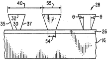
본 발명의 바람직한 일 실시예를 도 1, 1A 및 1B에 도시하였다. 부호 2로 나타낸 조명 시스템은 광 발생 수단 14, 광 수신면 17을 갖는 도파관 16 및 도파관 16에 광학적으로 접촉되는 투명 반사수단 18로 이루어져 있다. 유용한 광 발생수단 14의 예로는 반수수단에 또한 결합되어 광학 커플링을 상승시키는 레이저, 형광튜브(fluorescent tube), 광 방출 다이오드, 백열광, 태양광선 등을 포함한다. 도파관 16은 유리 혹은 중합체와 같은 어떠한 투명한 물질로 제조된다. 도 1에서 광 발생수단 14는 도파관 16과 광학적으로 결합되고 반사수단 18은 도파관 16에 접촉된다. 반사수단 18은 임의의 접착 증진층 26과 마이크로프리즘 28의 어레이로 이루어져 있다. 빛은 도파관 16을 통하여 TIR에 의해 반사되고 광 입력면 30을 거쳐 각 마이크로프리즘 28로 입사되고 측벽 33, 35 및 37로부터 반사되며, 광 출력면 32를 통하여 마이크로프리즘 28로부터 공간 조준된 광원으로 방출된다.One preferred embodiment of the present invention is shown in Figures 1, 1A and 1B. The illumination system, denoted by
도파관 16은 파장이 약 400-700nm 범위인 빛에 대하여 투명하다. 도파관 16의 굴절율은 약 1.40-1.65이다. 가장 바람직한 굴절율은 약 1.45-1.60이다. 도파관 16은 어떠한 투명한 고형물로 부터 제조될 수 있다. 바람직한 물질로는 투명한 중합체, 유리 및 용융 실리카를 포함한다. 상기 물질의 필요로 하는 특성으로는 장치의 전형적인 작동 온도에서의 기계적 안정성 및 광학 안정성이다. 가장 바람직한 물질은 유리, 아크릴, 폴리카보네이트 및 폴리에스테르이다.The
마이크로프리즘 28은 어떠한 투명한 고형물로 부터 제조될 수 있다. 바람직한 물질은 굴절률이 도파관 16의 굴절률과 같거나 그 이상인 것이다. 바람직한 물질의 굴절률은 약 1-40-1.65이다. 마이크로프리즘 28을 제조하는 한가지 방법으로는 사출성형법을 포함한다. 상기 방법에 유용한 물질로는 폴리카보네이트, 아크릴 및 폴리(4-메틸 펜텐)을 포함한다. 다른 제조 방법에서는 우레탄 아크릴레이트와 메타크릴레이트, 에스테르 아크릴레이트와 메타크릴레이트, 에폭시 아크릴레이트와 메타크릴레이트, (폴리)에틸렌 글리콜 아크릴레이트와 메타크릴레이트 및 비닐 함유 유기 단량체로 이루어진 아크릴레이트 단량체 혼합물을 광중합함으로써 형성된 중합체를 포함한다. 유용한 단량체로는 메틸 메타크릴레이트, n-부틸 아크릴레이트, 2-에틸헥실 아크릴레이트, 이소데실 아크릴레이트, 2-히드록시에틸 아크릴레이트, 2-히드록시프로필 아크릴레이트, 시클로헥실 아크릴레이트, 1,4-부탄디올 디아크릴레이트, 에톡시레이트화된 비스페놀 A 디아크릴레이트, 네오펜틸글리콜 디아크릴레이트, 디에틸렌글리콜 디아크릴레이트, 디에틸렌 글리콜 디메타크릴레이트, 1,6-헥산 디올 디아크릴레이트, 트리메틸올프로판 트리아크릴레이트, 펜타에리트리톨 트리아크릴레이트 및 펜타에리트리톨 테트라-아크릴레이트를 포함한다. 특히 유용한 것은 최소 일종의 단량체가 디아크릴레이트 혹은 트리아크릴레이트와 같은 다작용성 단량체로된 혼합물로, 이들은 반응된 광중합체내에서 교차결합의 망상 구조를 형성할 것이다. 사진 평판술(photolithography)로 형성되는 마이크로프리즘 28에 가장 바람직한 물질은 에톡시레이트화된 비스페놀 A 디아크릴레이트와 트리메틸올프로판 트리아크릴레이트의 혼합물을 광중합함으로써 형성되는 교차결합된 중합체이다. 마이크로프리즘 28은 간극 부분 36에 의해 분리된다. 간극 부분 36의 굴절율은 마이크로프리즘 28의 굴절률보다 작아야 한다. 간극 부분에 바람직한 물질로는 굴절율이 1.00인 공기 및 굴절율이 약 1.16-1.40인 플루오로중합체 물질을 포함한다. 가장 바람직한 물질은 공기이다.The
임의의 접착 증진층 26은 광 전송성이며, 마이크로프리즘 28이 예를 들어 광교차결합된 아크릴레이트 단량체 물질 혹은 사출 성형된 폴리카보네이트와 같은 중합체로부터 형성되는 것과 같은 방식으로 제조되는 경우에도 도파관 16에 강하게 접착되도록 하는 유기 물질이다. 이와 같은 물질은 이 기술 분야의 숙련된 자에게 잘 알려져 있다. 접착 증진층 26의 두께는 중요한 것은 아니며 다양하게 변할 수 있다. 본 발명의 바람직한 실시에서 접착층 26의 두께는 약 30㎛이하이다. 상기 마이크로프리즘은 정사각형, 직사각형 혹은 육각형과 같이, 어떠한 형태로 도파관 16상에 배열될 수 있다. 상기 마이크로프리즘은 광 수신면 17에 수직방향으로 반복거리 38(도 1)과 광 수신면 17에 평행방향으로 반복거리 40(도 1B)를 갖는다. 반복거리 38과 40은 같거나 다를 수 있으며, 표시장치의 해상도 및 크기에 따라 다양하게 변할 수 있다. 더욱이, 반복거리 38과 40은 광 발생수단 14로 부터 거리가 멀어짐에 따라 도파관 16 내부의 광도(light intensity, 빛의 세기)가 감소되는 것을 보상하기 위하여 도파관 16의 표면을 가로질러 변화될 수 있다. 상기 광도의 감소는어레이의 다른 마이크로프리즘에 의해 빛이 제거됨에 기인한 것이다. 상기 마이크로프리즘 28은 광 입력면 30, 바람직하게는 광 출력면 32이 평행한 광 입력면을 갖는 6-면체의 기하학적 형태를 형성하도록 구성되며, 여기서 광 출력면 32의 표면적은 광 입력면 30과 동일하거나 보다 넓다. 나아가 마이크로프리즘 28은 대향하여 위치하는 2쌍의 측벽 33, 34 및 35, 37으로 이루어지며, 여기서 상기 측벽은 평평한 반사면으로 구성된다. 바람직하게는, 각 측벽은 도파관 16을 통하여 전파되는 빛을 반사하고 재조준하는데 효과적이다. 바람직하게는 도파관 16 혹은 그위에 접착층 26과 측벽 33의 교차면은 빛의 평균 방향에 수직인 선을 형성한다. 예를 들면 도 1에서 도시된 바와 같이, 접착층 26에 측벽 33의 교차면은 광 수신면 17에 평행한 선을 형성하고 따라서 도파관 16을 통하여 이송되는 빛의 평균 방향에 수직이다.Any
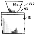
도 1A에 도시된 바와 같이, 각 마이크로프리즘 28은 측벽 33이 도파관 16 표면의 법선에 대하여 경사각 φ을 형성하도록 형성된다. 바람직한 경사각 φ는 약 15-50°이다. 보다 바람직한 경사각 φ는 약 20-40 °이다. 이 기술 분야에서 숙련된 기술자에게 명백한 바와 같이, 경사각 φ은 광 출력면의 법선에 대하여 공간으로 조준된 빛이 방출되는 각을 측정한다.As shown in FIG. 1A, each
도 1B를 참조하면, 측벽 35 및 37은 또한 도파관 16 표면의 법선에 대하여 경사각 θ를 형성한다. 바람직한 경사각 θ는 약 0-25 °이다. 보다 바람직한 경사각 θ는 약 2-20 °이다. 측벽 35 및 37에 관련된 경사각 θ은 동일한 것이 바람직하나 반드시 동일할 필요는 없다.1B, sidewalls 35 and 37 also form a tilt angle &thetas; with respect to the normal to the surface of
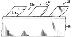
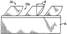
또한 마이크로프리즘 28의 최소 하나의 측벽은 둘 이상의 평평한 반사면으로 이루어져 마이크로프리즘의 반사도를 개선한다. 도 2A는 두 개의 평면 31과 31a를 갖는 측벽 33a를 예시하는 것이다. 측벽을 형성하는 평면의 수는 변화될 수 있다. 도 2B는 최소 하나의 측벽이 매우 미세한 다중 평면의 면으로 이루어져 측벽 33b가 아치형태로된 다른 실시예를 나타낸다. 또한 도 2C에서, 측벽 33c는 아치-형 반사면 42와 평평한 반사면 42a를 포함한다.Also, at least one side wall of the
도 1A 및 1B를 다시 참조하자면, 마이크로프리즘 28의 높이는 치수 50이며, 높이 50은 상기 표시 장치의 크기 및 해상도에 따라 다양하게 변할 것이다. 즉, 랩탑(laptop) 컴퓨터 표시 장치 및 항공전자공학(avionics) 표시 장치와 같은 소형 표시 장치에서는 대형 스크린, 평판 텔레비젼과 같은 대형 표시장치보다 치수가 크게 감소될 것이다.1A and 1B, the height of the micro-prism 28 is 50 in size, and the
마이크로프리즘 28의 길이는 치수 52 및 53이며, 길이 52는 광 입력면 30에 상응하고 길이 53은 광 출력면 32에 상응한다. 길이 53은 길이 52와 같거나 혹은 이보다 클 수 있다. 길이 52 및 53은 표시 장치의 크기 및 해상도에 따라 다양하게 변할 수 있다. 더욱이 길이 52는 광 발생 수단 14로 부터 거리가 멀어짐에 따라 도파관 16내부에 광도가 저감하는 것을 보상하기 위하여 광 전송 수단 16의 표면을 가로질러 다양하게 변할 수 있다. 즉, 광 발생 수단 14에 보다 근접한 마이크로프리즘 28은 광 발생 수단 14로 부터 보다 멀리 떨어진 마이크로프리즘에 비하여 치수 52가 보다 작을 수 있다. 상기 광도가 저감하는 어레이의 다른 마이크로프리즘에 의해 제거되는 빛에 기인한다. 길이 52 및 53의 최대값은 도 1의 반복 거리 38보다 작다.The length of the
마이크로프리즘 28의 폭 치수는 54및 55이며 폭 54는 광 입력면 30에 상응하고 폭 55는 광 출력면 32에 상응한다. 폭 54및 55는 표시 장치의 크기 및 해상도에 따라 매우 다양하게 변할 수 있으며 경사각 θ와 높이 50의 함수이다. 더욱이, 폭 54는 광 발생 수단 14로 부터 거리가 멀어짐에 따라 도파관 16 내부에 광도가 저감되는 것을 보상하기 위하여 광 전송 수단 16의 표면을 가로질러 변할 수 있다. 폭 54 및 55의 최대값은 반복 거리 40보다 작다. 길이 치수 52가 폭 치수 54보다 큰 것이 바람직하다. 길이 52 대 폭 54의 비가 1.2:1 - 5:1인 것이 바람직하다. 상기 비가 1.5:1 -3:1인 것이 보다 바람직하다.The width dimensions of the
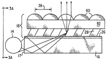
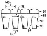
다른 실시예에서, 나아가 반사 수단 18은 도 3 및 3A에 도시된 바와 같이 마이크로 렌즈 80의 어레이를 포함한다. 마이크로렌즈 80은 마이크로프리즘 28에 광학적으로 결합된다. 마이크로렌즈 80은 마이크로프리즘 28에 기술된 것과 동일한 방법으로 제조될 수 있다. 상기 마이크로렌즈 80이 광중합으로 제조된다면, 마이크로프리즘 28에 대해 상기 개시된 것과 동일한 단량체로 제조되는 것이 바람직하며 굴절율은 마이크로프리즘 28의 굴절율과 동일하거나 혹은 실질적으로 동일하다. 그러나 예를 들어, 상기한 바와 같은 투명한 물질이 사용될 수 있다. 마이크로렌즈사이에 중심-대-중심 거리는 마이크로프리즘 28의 반복 거리 38 및 40에 직접적으로 연관된다. 즉, 각 마이크로프리즘 28에 대하여 각 마이크로프리즘 28의 출력면 32에 일렬로 배열된 상응하는 마이크로렌즈 80이 존재한다.In another embodiment, furthermore, the reflecting means 18 comprise an array of
스페이서(spacer) 82는 마이크로렌즈 80과 마이크로프리즘 28을 분리한다.스페이서 82의 두께는 마이크로렌즈 80에 의해 마이크로프리즘 28로 부터 빛을 조준하도록 최적화된다. 스페이서 82는 투명한 물질로 부터 제조될 수 있다. 바람직한 물질로는 투명한 중합체, 유리 및 용융 실리카를 포함한다. 바람직하게는 스페이서 82의 굴절율은 마이크로프리즘 28과 마이크로렌즈 80의 굴절율과 동일하거나 실질적으로 동일하다. 상기 물질의 필요로 하는 특성으로는 장치의 전형적인 작동 온도에서의 기계적 안정성 및 광학 안정성을 포함한다. 가장 바람직한 물질은 유리, 아크릴, 폴리카보네이트, 폴리에스테르 및 광중합된 아크릴레이트 단량체이다.A
단일 마이크로렌즈 80을 도 4에 도시하였다. 상기 마이크로렌즈는 구형 렌즈 혹은 반구형 렌즈 혹은 난시용 렌즈중 어느 하나일 수 있다. 마이크로렌즈 80의 자취가 반드시 구형일 필요는 없으며, 도 4A에 도시된 바와 같이 반복 거리 38 및 40과 각각 동일한 길이 86과 폭 87을 갖는 직사각형 형태일 수 있다.A
마이크로렌즈 80이 구형 렌즈이면, 상기 렌즈는 굴곡의 반경 84를 갖는 하나의 곡면을 갖는다. 상기 곡면의 반경은 상응하는 마이크로프리즘 어레이의 반복 거리 38과 40에 따라 다양하게 변할 수 있다. 마이크로렌즈 80이 마이크로프리즘 28에 의해 도파관 16에서 조준되는 모든 빛을 실질적으로 수집하도록, 마이크로렌즈 80의 f-값(f-number)은 비교적 작아야 한다. 마이크로렌즈 80의 f-값은 약 0.5-약 4.0일 수 있다. 보다 바람직한 f-값은 약 0.6-약 3.0이다.If the
본 발명의 또다른 대체 실시예를 도 5 및 5A에 도시하였다. 2 개의 광 발생 수단 14 및 14A는 도파관 16의 서로 대향하여 위치하는 2개의 광 수신면 17 및 17A에 인접하여 위치된다. 예시된 광 발생 수단뿐만 아니라, 광 발생 수단중 하나는반사면일 수 있다. 상기 반사면은 다른 광원으로 부터 나온 빛을 광 전송 수단 16내로 반사함으로써 광원으로서 작용한다. 마이크로프리즘 90의 어레이는 상기한 바와 유사한 방법으로 도파관 16에 접착된다. 상기 마이크로프리즘 90은 광입력면 92, 바람직하게는 광 출력면 94에 평행한 광 입력면 92로 이루어져 있으며, 상기 광 출력면 94의 표면적은 광 입력면 92보다 크다. 또한 마이크로프리즘 90은 대향하여 위치하는 두 쌍의 경사진 측벽 96,98 및 97,99로 이루어져 있다.Yet another alternative embodiment of the present invention is shown in Figures 5 and 5A. Two light generating means 14 and 14A are positioned adjacent to the two light receiving surfaces 17 and 17A located opposite to each other of the
측벽 96과 98은 각각 도파관 16 표면의 법선에 대하여 각 φ를 형성한다. 바람직하게는 측벽 96 및 98과 관련된 경사각 φ은 동일하나 반드시 경사각이 동일할 필요는 없다. 바람직하게는 도파관 16 혹은 그위의 접착층 26과 각 경사진 측벽 96 및 98의 교차면은 대향하여 위치하는 광 수신면 17 및 17A에 평행하며 따라서 도파관 16을 통하여 전송하는 빛의 평균 방향에 수직이다.The
도 5A를 참조하면, 측벽 97 및 99는 도파관 16 표면의 법선에 대하여 각각 각 θ로 형성된다. 바람직하게는 측벽 97과 99에 관한 경사각 θ는 동일하나 반드시 동일할 필요는 없다. 도파관 16 혹은 그위의 접착층 26과 각 경사진 측벽 97 및 99의 교차면은 대향하여 위치하는 광 수신면 17 및 17A에 대하여 수직이며, 따라서 도파관 16을 통하여 전송하는 빛의 평균 방향에 평행하다.Referring to FIG. 5A, the
또한, 마이크로프리즘 90의 최소 하나의 측벽은 하나 이상의 평평한 반사면으로 이루어지므로 마이크로프리즘의 반사도가 개선된다. 도 6A는 두 개의 평면 95 및 95a 를 갖는 측벽 98a를 예시하고 있다. 일 실시예에서 측벽 96a, 98a, 97a 및 99a는 도 6B 및 도 6C에 예시된 바와 같이 최소 2개의 평평한 반사면으로 이루어진다. 그러나 일반적으로 마이크로프리즘 90은 평면으로된 측벽 및 둘 이상의 평면을 갖는 측벽의 어떠한 결합일 수 있다.In addition, since at least one side wall of the
나아가 도 7A 및 7B는 최소 하나의 측벽, 예를 들어 98b가 다수의 매우 미세한 평면을 포함하여 측벽 98b가 아치 형태로된 실시예를 나타낸 것이다. 또한 측벽 98b는 아치-형 반사면 93과 평평한 반사 표면 93a를 포함한다.7A and 7B illustrate an embodiment in which at least one sidewall, e.g., 98b, includes a plurality of very fine planes so that the
마이크로프리즘 90의 높이는 치수 110을 갖으며 이는 마이크로프리즘 28의 높이 50과 같다. 마이크로프리즘 도파관 90의 길이 치수는 120 및 122이며 치수 122가 치수 120보다 작다. 길이 120과 122는 모두 경사각 φ 및 높이 110의 함수이다. 길이 120과 122는 표시 장치의 크기 및 해상도에 따라 다양하게 변할 수 있다. 더욱이 길이 120 및 122는 광 발생 수단 14 및 14A로 부터 거리가 멀어짐에 따라 도파관 16 내부에 광도가 감소되는 것을 보상하기 위하여 광 전송 수단 16의 표면을 가로질러 다양하게 변할 수 있다. 길이 120에 대한 최대값은 반복 거리 138보다 작다.The height of the
마이크로프리즘 28의 폭은 도 5A에 도시된 바와 같이 치수 130 및 132를 갖는다. 치수 132는 치수 130보다 작다. 폭 130과 132는 모두 경사각 θ과 높이 110의 함수이다. 폭 130 및 132는 상기 길이 120 및 122에 대하여 상기한 요인에 따라 다양하게 변화할 것이다. 폭 130에 대한 최대값은 반복 거리 140보다 작다. 길이 치수 122는 폭 치수 132보다 큰 것이 바람직하다. 길이 122 대 폭 132의 비는 바람직하게는 1.2:1 - 5:1, 보다 바람직하게는 1.5:1 - 3:1이다.The width of the
나아가 도 8-10에 개시된 본 발명의 다른 실시예는 마이크로프리즘 90에 광학적으로 결합된 마이크로렌즈 80의 어레이를 포함한다. 스페이서 82는 상기한 바와 같이 마이크로프리즘 90으로 부티 마이크로렌즈 80을 분리한다. 빛은 각 마이크로프리즘 90에서 공간으로 조준된 광원으로서 방출되며 하나 이상의 마이크로렌즈내로 입력된다. 바람직하게는 광원은 두 개의 마이크로렌즈에 조준된다. 마이크로프리즘 90으로 부터 방출되는 공간으로 조준된 광원은 마이크로렌즈 80에 의해 조준되어 실질적으로 시준된 광 패턴을 제공한다. 마이크로렌즈 사이의 중심-대-중심 거리는 마이크로프리즘 90의 반복 거리 138과 140에 직접적으로 연관되어 있다. 각 마이크로렌즈 80의 길이 86(도 4A)는 도 8 및 9에 도시된 바와 같이 인접한 마이크로프리즘에 동일 거리가 중첩되도록 마이크로프리즘 어레이에 대하여 배열된다. 각 마이크로렌즈의 폭 87은 도 10에 도시된 바와 같이 단일 마이크로렌즈에 대하여 배열된다.8-10 includes an array of
마이크로프리즘 28과 90 및 마이크로렌즈 80의 어레이는 사출 및 압축 성형을 포함하는 성형, 열간 압연 압착 주조를 포함하는 주조, 모울드내에서의 광중합 및 모울드를 사용하지 않는 광중합 공정과 같은 여러가지 기술로 제조될 수 있다. 바람직한 제조 기술은 마이크로프리즘 28 혹은 90, 마이크로렌즈 80의 어레이 및 스페이서 82로 이루어진 반사 수단 18을 단일 통합된 유니트로 제조하는 기술이다. 상기 기술의 잇점은 만일 어레이가 별도로 제조된 다음 상기한 바와 같은 관계로 접착되면 발생할 수 있는 마이크로프리즘과 마이크로렌즈의 어레이 사이의 정렬 오차(alignment error)가 제거될 수 있다는 것이다.The array of
상기 기술된 구체적인 실시예는 단지 본 발명의 원리를 예시한 것으로, 하기청구범위에 한정되는 본 발명의 범위 및 사상에서 이 기술 분야에서 숙련된 자에 의한 다양한 변형이 가능한 것이다.The specific embodiments described above are merely illustrative of the principles of the invention and are capable of various modifications by those skilled in the art in the scope and spirit of the invention as defined in the following claims.
본 발명은 조준되지 않은 광원에서 제거된 빛을 재조준하고 확산되지 않은 광원과 실질적으로 조준된 광원을 별도로 혹은 결합하여 제공하기 위한 복수의 광학 마이크로프리즘과 마이크로렌즈를 갖는 조명 시스템을 제공한다.The present invention provides an illumination system having a plurality of optical microprisms and microlenses for re-aiming light removed from an un-aimed light source and separately or conjointly providing a substantially collimated light source with an un-diffused light source.
상기 광학 조명 시스템은 에너지가 효율적이고 낮은 프로파일 어셈블리에 포함되는 산란되지 않거나 실질적으로 조준된 광원을 필요로 하는 적용처에서 이로운 것이다.The optical illumination system is advantageous in applications where energy is efficient and requires a non-scattered or substantially collimated light source included in a low profile assembly.
Claims (10)
Applications Claiming Priority (2)
| Application Number | Priority Date | Filing Date | Title |
|---|---|---|---|
| US32136894A | 1994-10-11 | 1994-10-11 | |
| US08/321,368 | 1994-10-11 |
Publications (2)
| Publication Number | Publication Date |
|---|---|
| KR970706468A KR970706468A (en) | 1997-11-03 |
| KR100437247B1 true KR100437247B1 (en) | 2004-09-08 |
Family
ID=23250324
Family Applications (1)
| Application Number | Title | Priority Date | Filing Date |
|---|---|---|---|
| KR1019970702314A KR100437247B1 (en) | 1994-10-11 | 1995-10-10 | Lighting system using an array of multi-planar microprisms |
Country Status (7)
| Country | Link |
|---|---|
| EP (1) | EP0787271B1 (en) |
| JP (1) | JP3532212B2 (en) |
| KR (1) | KR100437247B1 (en) |
| AU (1) | AU4199696A (en) |
| DE (1) | DE69521326T2 (en) |
| TW (1) | TW278142B (en) |
| WO (1) | WO1996011358A1 (en) |
Families Citing this family (17)
| Publication number | Priority date | Publication date | Assignee | Title |
|---|---|---|---|---|
| JP4111363B2 (en) | 1998-12-10 | 2008-07-02 | 株式会社エンプラス | Light guide plate, side light type surface light source device, and liquid crystal display device |
| JP2001051272A (en) | 1999-08-11 | 2001-02-23 | Semiconductor Energy Lab Co Ltd | Front light and electronic appliance |
| TW516164B (en) | 2000-04-21 | 2003-01-01 | Semiconductor Energy Lab | Self-light emitting device and electrical appliance using the same |
| EP1852736A1 (en) | 2000-12-13 | 2007-11-07 | Mitsubishi Rayon Co. Ltd. | Light source device |
| JP4606135B2 (en) * | 2004-11-19 | 2011-01-05 | アルプス電気株式会社 | Liquid crystal display device |
| US7452120B2 (en) * | 2006-03-24 | 2008-11-18 | Rohm And Haas Denmark Finance A/S | Illumination apparatus and film |
| JP4274239B2 (en) | 2006-12-27 | 2009-06-03 | ソニー株式会社 | Planar light source device, display device, and planar illumination method |
| WO2010070821A1 (en) * | 2008-12-16 | 2010-06-24 | オムロン株式会社 | Planar light source device |
| US8905610B2 (en) | 2009-01-26 | 2014-12-09 | Flex Lighting Ii, Llc | Light emitting device comprising a lightguide film |
| US9651729B2 (en) | 2010-04-16 | 2017-05-16 | Flex Lighting Ii, Llc | Reflective display comprising a frontlight with extraction features and a light redirecting optical element |
| US11009646B2 (en) | 2013-03-12 | 2021-05-18 | Azumo, Inc. | Film-based lightguide with interior light directing edges in a light mixing region |
| CA3064724C (en) * | 2017-06-21 | 2023-02-28 | Leia Inc. | Microprism multibeam element backlight and multiview display using same |
| KR102313983B1 (en) * | 2017-07-27 | 2021-10-18 | 엘지이노텍 주식회사 | Light control member and display device |
| CN113272693B (en) | 2018-08-30 | 2023-06-13 | 阿祖莫公司 | Film-based front light with angularly variable diffuser film |
| CN113678035A (en) | 2019-01-03 | 2021-11-19 | 阿祖莫公司 | Reflective display including light guide and light turning film that produce multiple illumination peaks |
| CN110161758B (en) * | 2019-06-24 | 2022-04-05 | 京东方科技集团股份有限公司 | Light conversion structure, backlight module and virtual reality display device |
| WO2021022307A1 (en) | 2019-08-01 | 2021-02-04 | Flex Lighting Ii, Llc | Lightguide with a light input edge between lateral edges of a folded strip |
Citations (2)
| Publication number | Priority date | Publication date | Assignee | Title |
|---|---|---|---|---|
| EP0292159A1 (en) * | 1987-05-08 | 1988-11-23 | Minnesota Mining And Manufacturing Company | High aspect ratio light fixture and film for use therein |
| US5396350A (en) * | 1993-11-05 | 1995-03-07 | Alliedsignal Inc. | Backlighting apparatus employing an array of microprisms |
Family Cites Families (3)
| Publication number | Priority date | Publication date | Assignee | Title |
|---|---|---|---|---|
| DE2736486C3 (en) * | 1976-08-13 | 1980-05-22 | Izon Corp., Stamford, Conn. (V.St.A.) | Optical device for recording and reading out micro information |
| DE3406191A1 (en) * | 1984-02-21 | 1985-09-26 | Schott Glaswerke, 6500 Mainz | ARRANGEMENT FOR ILLUMINATING OPTICAL OR OPTOELECTRONIC STRUCTURES |
| US5040878A (en) * | 1990-01-26 | 1991-08-20 | Dimension Technologies, Inc. | Illumination for transmissive displays |
-
1995
- 1995-10-03 TW TW084110313A patent/TW278142B/zh not_active IP Right Cessation
- 1995-10-10 JP JP51276396A patent/JP3532212B2/en not_active Expired - Lifetime
- 1995-10-10 KR KR1019970702314A patent/KR100437247B1/en not_active IP Right Cessation
- 1995-10-10 DE DE69521326T patent/DE69521326T2/en not_active Expired - Lifetime
- 1995-10-10 EP EP95940601A patent/EP0787271B1/en not_active Expired - Lifetime
- 1995-10-10 AU AU41996/96A patent/AU4199696A/en not_active Abandoned
- 1995-10-10 WO PCT/US1995/014272 patent/WO1996011358A1/en active IP Right Grant
Patent Citations (2)
| Publication number | Priority date | Publication date | Assignee | Title |
|---|---|---|---|---|
| EP0292159A1 (en) * | 1987-05-08 | 1988-11-23 | Minnesota Mining And Manufacturing Company | High aspect ratio light fixture and film for use therein |
| US5396350A (en) * | 1993-11-05 | 1995-03-07 | Alliedsignal Inc. | Backlighting apparatus employing an array of microprisms |
Also Published As
| Publication number | Publication date |
|---|---|
| EP0787271A1 (en) | 1997-08-06 |
| DE69521326T2 (en) | 2002-05-29 |
| AU4199696A (en) | 1996-05-02 |
| JP3532212B2 (en) | 2004-05-31 |
| DE69521326D1 (en) | 2001-07-19 |
| KR970706468A (en) | 1997-11-03 |
| WO1996011358A1 (en) | 1996-04-18 |
| TW278142B (en) | 1996-06-11 |
| EP0787271B1 (en) | 2001-06-13 |
| JPH10507306A (en) | 1998-07-14 |
Similar Documents
| Publication | Publication Date | Title |
|---|---|---|
| US6129439A (en) | Illumination system employing an array of multi-faceted microprisms | |
| US5739931A (en) | Illumination system employing an array of microprisms | |
| KR100397767B1 (en) | Lighting system using an array of microprisms | |
| KR100437247B1 (en) | Lighting system using an array of multi-planar microprisms | |
| KR100348734B1 (en) | Back light assembly for flat panel electronic display | |
| US6424786B1 (en) | Illumination assembly | |
| KR100778766B1 (en) | Optical element having an integral surface diffuser | |
| US5949933A (en) | Lenticular illumination system | |
| US7581850B2 (en) | Light guide plate and backlight module using the same | |
| US7670041B2 (en) | Backlight module | |
| JP2002506268A5 (en) | ||
| TW583462B (en) | Backlight assembly for collimated illumination | |
| JP2003215312A (en) | Optical element and optical system | |
| KR20070045479A (en) | Backlight module |
Legal Events
| Date | Code | Title | Description |
|---|---|---|---|
| A201 | Request for examination | ||
| E902 | Notification of reason for refusal | ||
| E902 | Notification of reason for refusal | ||
| E701 | Decision to grant or registration of patent right | ||
| GRNT | Written decision to grant | ||
| FPAY | Annual fee payment |
Payment date: 20120605 Year of fee payment: 9 |
|
| LAPS | Lapse due to unpaid annual fee |