JP7418400B2 - Diffractive optical elements and related systems and methods with mitigation of rebounce-induced light loss - Google Patents
Diffractive optical elements and related systems and methods with mitigation of rebounce-induced light loss Download PDFInfo
- Publication number
- JP7418400B2 JP7418400B2 JP2021503153A JP2021503153A JP7418400B2 JP 7418400 B2 JP7418400 B2 JP 7418400B2 JP 2021503153 A JP2021503153 A JP 2021503153A JP 2021503153 A JP2021503153 A JP 2021503153A JP 7418400 B2 JP7418400 B2 JP 7418400B2
- Authority
- JP
- Japan
- Prior art keywords
- waveguide
- light
- optical element
- reflective layer
- region
- Prior art date
- Legal status (The legal status is an assumption and is not a legal conclusion. Google has not performed a legal analysis and makes no representation as to the accuracy of the status listed.)
- Active
Links
- 230000003287 optical effect Effects 0.000 title claims description 495
- 238000000034 method Methods 0.000 title description 106
- 230000000116 mitigating effect Effects 0.000 title description 2
- 238000010168 coupling process Methods 0.000 claims description 110
- 238000005859 coupling reaction Methods 0.000 claims description 110
- 230000008878 coupling Effects 0.000 claims description 102
- 239000010410 layer Substances 0.000 description 355
- 229910052751 metal Inorganic materials 0.000 description 132
- 239000002184 metal Substances 0.000 description 132
- 239000000203 mixture Substances 0.000 description 123
- 239000007788 liquid Substances 0.000 description 113
- 238000000151 deposition Methods 0.000 description 53
- 230000033001 locomotion Effects 0.000 description 48
- 238000000576 coating method Methods 0.000 description 42
- 150000003839 salts Chemical class 0.000 description 39
- 239000000463 material Substances 0.000 description 34
- 238000006722 reduction reaction Methods 0.000 description 34
- 239000011248 coating agent Substances 0.000 description 33
- 210000000695 crystalline len Anatomy 0.000 description 33
- 239000000976 ink Substances 0.000 description 33
- 239000000758 substrate Substances 0.000 description 33
- 239000003638 chemical reducing agent Substances 0.000 description 32
- BQCADISMDOOEFD-UHFFFAOYSA-N Silver Chemical compound [Ag] BQCADISMDOOEFD-UHFFFAOYSA-N 0.000 description 31
- 229910052709 silver Inorganic materials 0.000 description 31
- 239000004332 silver Substances 0.000 description 31
- 239000003054 catalyst Substances 0.000 description 30
- 230000009467 reduction Effects 0.000 description 29
- 230000004308 accommodation Effects 0.000 description 27
- 238000012545 processing Methods 0.000 description 27
- 238000006243 chemical reaction Methods 0.000 description 23
- 210000002381 plasma Anatomy 0.000 description 22
- 230000008021 deposition Effects 0.000 description 19
- 230000005670 electromagnetic radiation Effects 0.000 description 18
- 238000002310 reflectometry Methods 0.000 description 18
- FOIXSVOLVBLSDH-UHFFFAOYSA-N Silver ion Chemical compound [Ag+] FOIXSVOLVBLSDH-UHFFFAOYSA-N 0.000 description 17
- 238000002203 pretreatment Methods 0.000 description 17
- 229920002120 photoresistant polymer Polymers 0.000 description 16
- 239000004094 surface-active agent Substances 0.000 description 16
- 239000003086 colorant Substances 0.000 description 15
- 210000001747 pupil Anatomy 0.000 description 15
- 210000001525 retina Anatomy 0.000 description 15
- KDLHZDBZIXYQEI-UHFFFAOYSA-N Palladium Chemical compound [Pd] KDLHZDBZIXYQEI-UHFFFAOYSA-N 0.000 description 14
- 230000008569 process Effects 0.000 description 14
- 238000001465 metallisation Methods 0.000 description 13
- VYPSYNLAJGMNEJ-UHFFFAOYSA-N Silicium dioxide Chemical compound O=[Si]=O VYPSYNLAJGMNEJ-UHFFFAOYSA-N 0.000 description 11
- 229910021645 metal ion Inorganic materials 0.000 description 11
- 239000002923 metal particle Substances 0.000 description 11
- 150000002739 metals Chemical class 0.000 description 11
- 229910052782 aluminium Inorganic materials 0.000 description 10
- XAGFODPZIPBFFR-UHFFFAOYSA-N aluminium Chemical compound [Al] XAGFODPZIPBFFR-UHFFFAOYSA-N 0.000 description 10
- 238000005240 physical vapour deposition Methods 0.000 description 10
- 230000001902 propagating effect Effects 0.000 description 10
- 239000000376 reactant Substances 0.000 description 10
- 238000010521 absorption reaction Methods 0.000 description 9
- 150000001720 carbohydrates Chemical class 0.000 description 9
- 235000014633 carbohydrates Nutrition 0.000 description 9
- 239000000835 fiber Substances 0.000 description 9
- 238000002347 injection Methods 0.000 description 9
- 239000007924 injection Substances 0.000 description 9
- 230000000007 visual effect Effects 0.000 description 9
- 238000007704 wet chemistry method Methods 0.000 description 9
- 230000002350 accommodative effect Effects 0.000 description 8
- 230000003190 augmentative effect Effects 0.000 description 8
- 230000008859 change Effects 0.000 description 8
- 238000004891 communication Methods 0.000 description 8
- 230000009969 flowable effect Effects 0.000 description 8
- 239000000126 substance Substances 0.000 description 8
- 238000007740 vapor deposition Methods 0.000 description 8
- 241000153282 Theope Species 0.000 description 7
- ATJFFYVFTNAWJD-UHFFFAOYSA-N Tin Chemical compound [Sn] ATJFFYVFTNAWJD-UHFFFAOYSA-N 0.000 description 7
- 239000002585 base Substances 0.000 description 7
- 230000015572 biosynthetic process Effects 0.000 description 7
- 239000003795 chemical substances by application Substances 0.000 description 7
- 239000006185 dispersion Substances 0.000 description 7
- 229910052763 palladium Inorganic materials 0.000 description 7
- 230000008447 perception Effects 0.000 description 7
- 230000002829 reductive effect Effects 0.000 description 7
- 238000001429 visible spectrum Methods 0.000 description 7
- QGZKDVFQNNGYKY-UHFFFAOYSA-N Ammonia Chemical compound N QGZKDVFQNNGYKY-UHFFFAOYSA-N 0.000 description 6
- 238000010586 diagram Methods 0.000 description 6
- 238000000635 electron micrograph Methods 0.000 description 6
- 238000005516 engineering process Methods 0.000 description 6
- 238000004519 manufacturing process Methods 0.000 description 6
- 239000002245 particle Substances 0.000 description 6
- 238000009832 plasma treatment Methods 0.000 description 6
- 238000001556 precipitation Methods 0.000 description 6
- 230000004044 response Effects 0.000 description 6
- XLYOFNOQVPJJNP-UHFFFAOYSA-N water Substances O XLYOFNOQVPJJNP-UHFFFAOYSA-N 0.000 description 6
- 239000004973 liquid crystal related substance Substances 0.000 description 5
- 239000000377 silicon dioxide Substances 0.000 description 5
- 125000006850 spacer group Chemical group 0.000 description 5
- 238000012360 testing method Methods 0.000 description 5
- CSCPPACGZOOCGX-UHFFFAOYSA-N Acetone Chemical compound CC(C)=O CSCPPACGZOOCGX-UHFFFAOYSA-N 0.000 description 4
- 230000004888 barrier function Effects 0.000 description 4
- 210000004556 brain Anatomy 0.000 description 4
- KRVSOGSZCMJSLX-UHFFFAOYSA-L chromic acid Substances O[Cr](O)(=O)=O KRVSOGSZCMJSLX-UHFFFAOYSA-L 0.000 description 4
- 238000005253 cladding Methods 0.000 description 4
- 230000000694 effects Effects 0.000 description 4
- 238000000605 extraction Methods 0.000 description 4
- 230000006870 function Effects 0.000 description 4
- AWJWCTOOIBYHON-UHFFFAOYSA-N furo[3,4-b]pyrazine-5,7-dione Chemical compound C1=CN=C2C(=O)OC(=O)C2=N1 AWJWCTOOIBYHON-UHFFFAOYSA-N 0.000 description 4
- 238000007781 pre-processing Methods 0.000 description 4
- 230000002207 retinal effect Effects 0.000 description 4
- 239000007787 solid Substances 0.000 description 4
- 229930091371 Fructose Natural products 0.000 description 3
- 239000005715 Fructose Substances 0.000 description 3
- RFSUNEUAIZKAJO-ARQDHWQXSA-N Fructose Chemical compound OC[C@H]1O[C@](O)(CO)[C@@H](O)[C@@H]1O RFSUNEUAIZKAJO-ARQDHWQXSA-N 0.000 description 3
- 239000013626 chemical specie Substances 0.000 description 3
- 239000002131 composite material Substances 0.000 description 3
- 230000007423 decrease Effects 0.000 description 3
- 238000010304 firing Methods 0.000 description 3
- 239000012535 impurity Substances 0.000 description 3
- 230000000670 limiting effect Effects 0.000 description 3
- 229910001338 liquidmetal Inorganic materials 0.000 description 3
- 239000002905 metal composite material Substances 0.000 description 3
- GGCZERPQGJTIQP-UHFFFAOYSA-N sodium;9,10-dioxoanthracene-2-sulfonic acid Chemical compound [Na+].C1=CC=C2C(=O)C3=CC(S(=O)(=O)O)=CC=C3C(=O)C2=C1 GGCZERPQGJTIQP-UHFFFAOYSA-N 0.000 description 3
- 239000002904 solvent Substances 0.000 description 3
- 241000894007 species Species 0.000 description 3
- 238000005507 spraying Methods 0.000 description 3
- -1 water) Chemical class 0.000 description 3
- WQZGKKKJIJFFOK-GASJEMHNSA-N Glucose Natural products OC[C@H]1OC(O)[C@H](O)[C@@H](O)[C@@H]1O WQZGKKKJIJFFOK-GASJEMHNSA-N 0.000 description 2
- 239000000853 adhesive Substances 0.000 description 2
- 230000001070 adhesive effect Effects 0.000 description 2
- 238000013459 approach Methods 0.000 description 2
- 239000007864 aqueous solution Substances 0.000 description 2
- 238000003491 array Methods 0.000 description 2
- 230000008901 benefit Effects 0.000 description 2
- WQZGKKKJIJFFOK-VFUOTHLCSA-N beta-D-glucose Chemical compound OC[C@H]1O[C@@H](O)[C@H](O)[C@@H](O)[C@@H]1O WQZGKKKJIJFFOK-VFUOTHLCSA-N 0.000 description 2
- 239000006227 byproduct Substances 0.000 description 2
- 239000003153 chemical reaction reagent Substances 0.000 description 2
- 238000009792 diffusion process Methods 0.000 description 2
- 238000009826 distribution Methods 0.000 description 2
- 210000000613 ear canal Anatomy 0.000 description 2
- 238000005530 etching Methods 0.000 description 2
- 230000004438 eyesight Effects 0.000 description 2
- 239000011521 glass Substances 0.000 description 2
- 239000008103 glucose Substances 0.000 description 2
- 210000003128 head Anatomy 0.000 description 2
- 238000007641 inkjet printing Methods 0.000 description 2
- 238000005259 measurement Methods 0.000 description 2
- 238000012986 modification Methods 0.000 description 2
- 230000004048 modification Effects 0.000 description 2
- 239000002086 nanomaterial Substances 0.000 description 2
- 229910000069 nitrogen hydride Inorganic materials 0.000 description 2
- 239000003002 pH adjusting agent Substances 0.000 description 2
- PIBWKRNGBLPSSY-UHFFFAOYSA-L palladium(II) chloride Chemical compound Cl[Pd]Cl PIBWKRNGBLPSSY-UHFFFAOYSA-L 0.000 description 2
- 230000036961 partial effect Effects 0.000 description 2
- 230000002093 peripheral effect Effects 0.000 description 2
- 239000002244 precipitate Substances 0.000 description 2
- 230000011514 reflex Effects 0.000 description 2
- 230000000717 retained effect Effects 0.000 description 2
- 238000004088 simulation Methods 0.000 description 2
- 239000003381 stabilizer Substances 0.000 description 2
- 238000004381 surface treatment Methods 0.000 description 2
- HPGGPRDJHPYFRM-UHFFFAOYSA-J tin(iv) chloride Chemical compound Cl[Sn](Cl)(Cl)Cl HPGGPRDJHPYFRM-UHFFFAOYSA-J 0.000 description 2
- 238000005406 washing Methods 0.000 description 2
- 238000003631 wet chemical etching Methods 0.000 description 2
- 241000256837 Apidae Species 0.000 description 1
- 241000473391 Archosargus rhomboidalis Species 0.000 description 1
- 241000692870 Inachis io Species 0.000 description 1
- 239000004983 Polymer Dispersed Liquid Crystal Substances 0.000 description 1
- XUIMIQQOPSSXEZ-UHFFFAOYSA-N Silicon Chemical compound [Si] XUIMIQQOPSSXEZ-UHFFFAOYSA-N 0.000 description 1
- 229930006000 Sucrose Natural products 0.000 description 1
- CZMRCDWAGMRECN-UGDNZRGBSA-N Sucrose Chemical compound O[C@H]1[C@H](O)[C@@H](CO)O[C@@]1(CO)O[C@@H]1[C@H](O)[C@@H](O)[C@H](O)[C@@H](CO)O1 CZMRCDWAGMRECN-UGDNZRGBSA-N 0.000 description 1
- 229910021626 Tin(II) chloride Inorganic materials 0.000 description 1
- 239000002253 acid Substances 0.000 description 1
- 230000002411 adverse Effects 0.000 description 1
- 238000013019 agitation Methods 0.000 description 1
- 230000004075 alteration Effects 0.000 description 1
- 229910021529 ammonia Inorganic materials 0.000 description 1
- 238000000137 annealing Methods 0.000 description 1
- 230000000712 assembly Effects 0.000 description 1
- 238000000429 assembly Methods 0.000 description 1
- 239000011230 binding agent Substances 0.000 description 1
- 239000007767 bonding agent Substances 0.000 description 1
- 238000004364 calculation method Methods 0.000 description 1
- 230000015556 catabolic process Effects 0.000 description 1
- 229910052804 chromium Inorganic materials 0.000 description 1
- 239000011651 chromium Substances 0.000 description 1
- 230000001886 ciliary effect Effects 0.000 description 1
- 238000004140 cleaning Methods 0.000 description 1
- 150000001875 compounds Chemical class 0.000 description 1
- 230000008602 contraction Effects 0.000 description 1
- 210000004087 cornea Anatomy 0.000 description 1
- 238000005520 cutting process Methods 0.000 description 1
- 238000013500 data storage Methods 0.000 description 1
- 230000003247 decreasing effect Effects 0.000 description 1
- 230000007547 defect Effects 0.000 description 1
- 238000006731 degradation reaction Methods 0.000 description 1
- 230000006866 deterioration Effects 0.000 description 1
- 238000011161 development Methods 0.000 description 1
- 238000002845 discoloration Methods 0.000 description 1
- 238000010494 dissociation reaction Methods 0.000 description 1
- 230000005593 dissociations Effects 0.000 description 1
- 238000000203 droplet dispensing Methods 0.000 description 1
- 238000001035 drying Methods 0.000 description 1
- 238000007772 electroless plating Methods 0.000 description 1
- 238000011049 filling Methods 0.000 description 1
- 238000010438 heat treatment Methods 0.000 description 1
- 238000003384 imaging method Methods 0.000 description 1
- 230000006872 improvement Effects 0.000 description 1
- 238000011065 in-situ storage Methods 0.000 description 1
- 238000011534 incubation Methods 0.000 description 1
- 230000002401 inhibitory effect Effects 0.000 description 1
- 210000003041 ligament Anatomy 0.000 description 1
- 230000031700 light absorption Effects 0.000 description 1
- 239000007791 liquid phase Substances 0.000 description 1
- 238000012544 monitoring process Methods 0.000 description 1
- 210000003205 muscle Anatomy 0.000 description 1
- 230000006855 networking Effects 0.000 description 1
- 239000013307 optical fiber Substances 0.000 description 1
- 230000002688 persistence Effects 0.000 description 1
- 230000000704 physical effect Effects 0.000 description 1
- 230000004962 physiological condition Effects 0.000 description 1
- 230000035790 physiological processes and functions Effects 0.000 description 1
- 239000002243 precursor Substances 0.000 description 1
- 239000000047 product Substances 0.000 description 1
- 230000000644 propagated effect Effects 0.000 description 1
- 239000011241 protective layer Substances 0.000 description 1
- 229910052710 silicon Inorganic materials 0.000 description 1
- 239000010703 silicon Substances 0.000 description 1
- 229910052814 silicon oxide Inorganic materials 0.000 description 1
- 150000003378 silver Chemical class 0.000 description 1
- 239000002356 single layer Substances 0.000 description 1
- 239000000243 solution Substances 0.000 description 1
- 238000001228 spectrum Methods 0.000 description 1
- 239000007921 spray Substances 0.000 description 1
- 235000011150 stannous chloride Nutrition 0.000 description 1
- 230000003068 static effect Effects 0.000 description 1
- 230000000638 stimulation Effects 0.000 description 1
- 239000005720 sucrose Substances 0.000 description 1
- AXZWODMDQAVCJE-UHFFFAOYSA-L tin(II) chloride (anhydrous) Chemical compound [Cl-].[Cl-].[Sn+2] AXZWODMDQAVCJE-UHFFFAOYSA-L 0.000 description 1
- 210000001519 tissue Anatomy 0.000 description 1
- 239000012780 transparent material Substances 0.000 description 1
- 230000004304 visual acuity Effects 0.000 description 1
- 230000016776 visual perception Effects 0.000 description 1
- 238000012800 visualization Methods 0.000 description 1
- 238000001039 wet etching Methods 0.000 description 1
Images


Classifications
-
- G—PHYSICS
- G02—OPTICS
- G02B—OPTICAL ELEMENTS, SYSTEMS OR APPARATUS
- G02B27/00—Optical systems or apparatus not provided for by any of the groups G02B1/00 - G02B26/00, G02B30/00
- G02B27/42—Diffraction optics, i.e. systems including a diffractive element being designed for providing a diffractive effect
- G02B27/4205—Diffraction optics, i.e. systems including a diffractive element being designed for providing a diffractive effect having a diffractive optical element [DOE] contributing to image formation, e.g. whereby modulation transfer function MTF or optical aberrations are relevant
-
- G—PHYSICS
- G02—OPTICS
- G02B—OPTICAL ELEMENTS, SYSTEMS OR APPARATUS
- G02B27/00—Optical systems or apparatus not provided for by any of the groups G02B1/00 - G02B26/00, G02B30/00
- G02B27/01—Head-up displays
- G02B27/017—Head mounted
- G02B27/0172—Head mounted characterised by optical features
-
- C—CHEMISTRY; METALLURGY
- C03—GLASS; MINERAL OR SLAG WOOL
- C03C—CHEMICAL COMPOSITION OF GLASSES, GLAZES OR VITREOUS ENAMELS; SURFACE TREATMENT OF GLASS; SURFACE TREATMENT OF FIBRES OR FILAMENTS MADE FROM GLASS, MINERALS OR SLAGS; JOINING GLASS TO GLASS OR OTHER MATERIALS
- C03C25/00—Surface treatment of fibres or filaments made from glass, minerals or slags
- C03C25/10—Coating
- C03C25/104—Coating to obtain optical fibres
- C03C25/106—Single coatings
- C03C25/1061—Inorganic coatings
- C03C25/1063—Metals
-
- G—PHYSICS
- G02—OPTICS
- G02B—OPTICAL ELEMENTS, SYSTEMS OR APPARATUS
- G02B27/00—Optical systems or apparatus not provided for by any of the groups G02B1/00 - G02B26/00, G02B30/00
- G02B27/10—Beam splitting or combining systems
- G02B27/1006—Beam splitting or combining systems for splitting or combining different wavelengths
- G02B27/102—Beam splitting or combining systems for splitting or combining different wavelengths for generating a colour image from monochromatic image signal sources
- G02B27/1046—Beam splitting or combining systems for splitting or combining different wavelengths for generating a colour image from monochromatic image signal sources for use with transmissive spatial light modulators
-
- G—PHYSICS
- G02—OPTICS
- G02B—OPTICAL ELEMENTS, SYSTEMS OR APPARATUS
- G02B27/00—Optical systems or apparatus not provided for by any of the groups G02B1/00 - G02B26/00, G02B30/00
- G02B27/42—Diffraction optics, i.e. systems including a diffractive element being designed for providing a diffractive effect
- G02B27/4233—Diffraction optics, i.e. systems including a diffractive element being designed for providing a diffractive effect having a diffractive element [DOE] contributing to a non-imaging application
-
- G—PHYSICS
- G02—OPTICS
- G02B—OPTICAL ELEMENTS, SYSTEMS OR APPARATUS
- G02B5/00—Optical elements other than lenses
- G02B5/18—Diffraction gratings
- G02B5/1847—Manufacturing methods
- G02B5/1857—Manufacturing methods using exposure or etching means, e.g. holography, photolithography, exposure to electron or ion beams
-
- G—PHYSICS
- G02—OPTICS
- G02B—OPTICAL ELEMENTS, SYSTEMS OR APPARATUS
- G02B5/00—Optical elements other than lenses
- G02B5/18—Diffraction gratings
- G02B5/1861—Reflection gratings characterised by their structure, e.g. step profile, contours of substrate or grooves, pitch variations, materials
-
- G—PHYSICS
- G02—OPTICS
- G02B—OPTICAL ELEMENTS, SYSTEMS OR APPARATUS
- G02B6/00—Light guides; Structural details of arrangements comprising light guides and other optical elements, e.g. couplings
-
- G—PHYSICS
- G02—OPTICS
- G02B—OPTICAL ELEMENTS, SYSTEMS OR APPARATUS
- G02B6/00—Light guides; Structural details of arrangements comprising light guides and other optical elements, e.g. couplings
- G02B6/0001—Light guides; Structural details of arrangements comprising light guides and other optical elements, e.g. couplings specially adapted for lighting devices or systems
- G02B6/0011—Light guides; Structural details of arrangements comprising light guides and other optical elements, e.g. couplings specially adapted for lighting devices or systems the light guides being planar or of plate-like form
- G02B6/0013—Means for improving the coupling-in of light from the light source into the light guide
- G02B6/0023—Means for improving the coupling-in of light from the light source into the light guide provided by one optical element, or plurality thereof, placed between the light guide and the light source, or around the light source
- G02B6/0026—Wavelength selective element, sheet or layer, e.g. filter or grating
-
- G—PHYSICS
- G02—OPTICS
- G02B—OPTICAL ELEMENTS, SYSTEMS OR APPARATUS
- G02B6/00—Light guides; Structural details of arrangements comprising light guides and other optical elements, e.g. couplings
- G02B6/0001—Light guides; Structural details of arrangements comprising light guides and other optical elements, e.g. couplings specially adapted for lighting devices or systems
- G02B6/0011—Light guides; Structural details of arrangements comprising light guides and other optical elements, e.g. couplings specially adapted for lighting devices or systems the light guides being planar or of plate-like form
- G02B6/0033—Means for improving the coupling-out of light from the light guide
- G02B6/005—Means for improving the coupling-out of light from the light guide provided by one optical element, or plurality thereof, placed on the light output side of the light guide
- G02B6/0055—Reflecting element, sheet or layer
-
- G—PHYSICS
- G02—OPTICS
- G02B—OPTICAL ELEMENTS, SYSTEMS OR APPARATUS
- G02B6/00—Light guides; Structural details of arrangements comprising light guides and other optical elements, e.g. couplings
- G02B6/0001—Light guides; Structural details of arrangements comprising light guides and other optical elements, e.g. couplings specially adapted for lighting devices or systems
- G02B6/0011—Light guides; Structural details of arrangements comprising light guides and other optical elements, e.g. couplings specially adapted for lighting devices or systems the light guides being planar or of plate-like form
- G02B6/0075—Arrangements of multiple light guides
- G02B6/0076—Stacked arrangements of multiple light guides of the same or different cross-sectional area
-
- G—PHYSICS
- G02—OPTICS
- G02B—OPTICAL ELEMENTS, SYSTEMS OR APPARATUS
- G02B6/00—Light guides; Structural details of arrangements comprising light guides and other optical elements, e.g. couplings
- G02B6/24—Coupling light guides
- G02B6/26—Optical coupling means
-
- G—PHYSICS
- G06—COMPUTING; CALCULATING OR COUNTING
- G06T—IMAGE DATA PROCESSING OR GENERATION, IN GENERAL
- G06T19/00—Manipulating 3D models or images for computer graphics
- G06T19/006—Mixed reality
-
- G—PHYSICS
- G02—OPTICS
- G02B—OPTICAL ELEMENTS, SYSTEMS OR APPARATUS
- G02B27/00—Optical systems or apparatus not provided for by any of the groups G02B1/00 - G02B26/00, G02B30/00
- G02B27/01—Head-up displays
- G02B27/017—Head mounted
- G02B2027/0178—Eyeglass type
-
- G—PHYSICS
- G02—OPTICS
- G02B—OPTICAL ELEMENTS, SYSTEMS OR APPARATUS
- G02B6/00—Light guides; Structural details of arrangements comprising light guides and other optical elements, e.g. couplings
- G02B6/10—Light guides; Structural details of arrangements comprising light guides and other optical elements, e.g. couplings of the optical waveguide type
Landscapes
- Physics & Mathematics (AREA)
- General Physics & Mathematics (AREA)
- Optics & Photonics (AREA)
- Engineering & Computer Science (AREA)
- Chemical & Material Sciences (AREA)
- Life Sciences & Earth Sciences (AREA)
- Computer Hardware Design (AREA)
- Computer Graphics (AREA)
- Theoretical Computer Science (AREA)
- Software Systems (AREA)
- General Engineering & Computer Science (AREA)
- Inorganic Chemistry (AREA)
- General Life Sciences & Earth Sciences (AREA)
- Manufacturing & Machinery (AREA)
- Chemical Kinetics & Catalysis (AREA)
- Geochemistry & Mineralogy (AREA)
- General Chemical & Material Sciences (AREA)
- Organic Chemistry (AREA)
- Materials Engineering (AREA)
- Optical Couplings Of Light Guides (AREA)
- Optical Elements Other Than Lenses (AREA)
- Mechanical Optical Scanning Systems (AREA)
- Diffracting Gratings Or Hologram Optical Elements (AREA)
Description
(優先権の主張)
本願は、35U.S.C.§119(e)下、両方とも、参照することによって、その全体として、あらゆる目的のために、本明細書に組み込まれる、2018年7月24日に出願され、「DIFFRACTIVE OPTICAL ELEMENTS WITH MITIGATION OF REBOUNCE-INDUCED LIGHT LOSS AND DISPLAY DEVICES CONTAINING THE SAME」と題された、米国仮出願第62/702,707号、および2018年10月17日に出願され、「WAVEGUIDES HAVING HIGHLY REFLECTIVE LAYERS AND METHODS FOR FORMING」と題された、米国仮出願第62/747,032号の優先権を主張する。
(Claim of priority)
This application is based on 35U. S. C. § 119(e), both filed on July 24, 2018 and incorporated herein by reference in its entirety for all purposes. - INDUCED LIGHT LOSS AND DISPLAY DEVICES CONTAINING THE SAME,” and U.S. Provisional Application No. 62/702,707, filed October 17, 2018, entitled “WAVEGUIDES HAVING HIGHLY R EFLECTIVE LAYERS AND METHODS FOR FORMING” Claims priority to U.S. Provisional Application No. 62/747,032, entitled U.S. Provisional Application No. 62/747,032.
(参照による組み込み)
本願は、参照することによって、以下の特許出願、すなわち、2014年11月27日に出願され、2015年7月23日に米国特許公開第2015/0205126号として公開された、米国特許出願第14/555,585号、2015年4月18日に出願され、2015年10月22日に米国特許公開第2015/0302652号として公開された、米国特許出願第14/690,401号、2014年3月14日に出願され、2016年8月16日に発行された、現米国特許第9,417,452号である、米国特許出願第14/212,961号、2014年7月14日に出願され、2015年10月29日に米国特許公開第2015/0309263号として公開された、米国特許出願第14/331,218号、および2018年4月16日に出願された、米国特許出願第15/954,419号のそれぞれの全体を組み込む。
(Inclusion by reference)
This application is hereby incorporated by reference into the following patent applications: U.S. Patent Application No. 14, filed on November 27, 2014, and published as U.S. Patent Publication No. US Pat. U.S. Patent Application No. 14/212,961, filed July 14, 2014, currently U.S. Patent No. 9,417,452, filed on August 14, 2016. U.S. Patent Application No. 14/331,218, published as U.S. Patent Publication No. 2015/0309263 on October 29, 2015, and U.S. Patent Application No. 15, filed April 16, 2018. No./954,419, each of which is incorporated in its entirety.
本開示は、ディスプレイシステムに関し、より具体的には、拡張および仮想現実ディスプレイシステムに関する。 TECHNICAL FIELD This disclosure relates to display systems and, more particularly, to augmented and virtual reality display systems.
現代のコンピューティングおよびディスプレイ技術は、いわゆる「仮想現実」または「拡張現実」体験のためのシステムの開発を促進しており、デジタル的に再現された画像またはその一部が、現実であるように見える、またはそのように知覚され得る様式でユーザに提示される。仮想現実、すなわち、「VR」シナリオは、典型的には、他の実際の実世界の視覚的入力に対する透過性を伴わずに、デジタルまたは仮想画像情報の提示を伴い、拡張現実、すなわち、「AR」シナリオは、典型的には、ユーザの周囲の実際の世界の可視化に対する拡張としてのデジタルまたは仮想画像情報の提示を伴う。複合現実または「MR」シナリオは、一種のARシナリオであって、典型的には、自然世界の中に統合され、それに応答する、仮想オブジェクトを伴う。例えば、MRシナリオは、実世界内のオブジェクトによってブロックされて見える、または別様にそれと相互作用するように知覚される、AR画像コンテンツを含んでもよい。 Modern computing and display technologies have facilitated the development of systems for so-called "virtual reality" or "augmented reality" experiences, in which digitally reproduced images, or parts thereof, appear as if they were real. Presented to the user in a manner that can be seen or perceived as such. Virtual reality, or "VR" scenarios typically involve the presentation of digital or virtual image information without transparency to other actual, real-world visual input; "AR" scenarios typically involve the presentation of digital or virtual image information as an extension to the visualization of the real world around the user. Mixed reality or "MR" scenarios are a type of AR scenario that typically involve virtual objects that are integrated into and responsive to the natural world. For example, an MR scenario may include AR image content that appears blocked by or otherwise perceived to interact with objects in the real world.
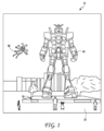
図1を参照すると、拡張現実場面10が、描写されている。AR技術のユーザには、背景における人々、木々、背景における建物、コンクリートプラットフォーム30を特徴とする、実世界公園状設定20が見える。ユーザはまた、実世界プラットフォーム30上に立っているロボット像40と、マルハナバチの擬人化のように見える、飛んでいる漫画のようなアバタキャラクタ50等の「仮想コンテンツ」を「見ている」と知覚する。これらの要素50、40は、実世界内に存在しないという点で、「仮想」である。ヒトの視知覚系が、複雑であるため、他の仮想または実世界画像要素間における仮想画像要素の快適で、自然のような感覚で、かつ豊かな提示を促進する、AR技術の生成は、困難である。
Referring to FIG. 1, an augmented reality scene 10 is depicted. A user of the AR technology sees a real-world park-
いくつかの側面は、画像をユーザの眼に投影するためのディスプレイシステムを含む。ディスプレイシステムは、第1の主要表面と、第1の主要表面に対向する、第2の主要表面とを備える、導波管と、光のビームを導波管の第2の主要表面に向かって投影するように構成される、投影光学系と、導波管の第2の主要表面上に配置される、内部結合光学要素であって、内部結合光学要素は、投影光学系からの光を内部結合するように構成される、回折領域を備え、投影光学系からの光を全内部反射によって導波管内を第1の方向に伝搬するように再指向するように構成される、内部結合光学要素とを備える。回折領域は、投影光学系からの光のビームの第1の部分が、回折領域上に入射し、投影光学系からの光のビームの第2の部分が、回折領域上に入射せずに、導波管上に衝突するようにサイズ決めおよび成形される。 Some aspects include a display system for projecting images to a user's eyes. The display system includes a waveguide comprising a first major surface and a second major surface opposite the first major surface, and directing a beam of light toward the second major surface of the waveguide. a projection optical system configured to project and an internally coupled optical element disposed on a second major surface of the waveguide, the internally coupled optical element configured to internally transmit light from the projection optical system; an internally coupling optical element configured to couple, comprising a diffractive region, and configured to redirect light from the projection optical system to propagate in a first direction within the waveguide by total internal reflection; Equipped with. The diffractive region is configured such that a first portion of the beam of light from the projection optical system is incident on the diffractive region and a second portion of the beam of light from the projection optical system is not incident on the diffractive region. Sized and shaped to impinge on the waveguide.
回折領域は、高効率回折領域であってもよく、内部結合光学要素は、投影光学系からの光のビームの第2の部分が低効率回折領域上に入射するようにサイズ決めおよび成形される、低効率回折領域をさらに備える。高効率回折領域は、金属化された格子部分を備える、反射性回折領域であってもよく、低効率回折領域は、非金属化された格子部分を備えてもよい。光のビームの第2の部分は、導波管の中に内部結合されずに、第2の主要表面を通して、導波管から外に伝搬し得る。光のビームの第2の部分は、光のビームの第1の部分に対してより低い効率で導波管の中に内部結合され得る。回折領域は、投影光学系からの光のビームのビーム軸における伝搬方向と垂直な対称軸を中心として反射非対称であってもよい。導波管は、導波管スタックの一部であってもよく、導波管スタックはさらに、第1の主要表面および第2の主要表面を備える、第2の導波管と、第2の導波管の第2の主要表面上に配置される、第2の内部結合光学要素であって、光のビームによって画定された面積の回折領域によって被覆される割合に対して、投影光学系からの光の第2のビームによって画定された面積のより大きい割合を被覆する、第2の回折領域を備える、第2の内部結合光学要素とを備える。第2の回折領域は、第2の光のビームの実質的に全てを内部結合するように構成されてもよい。第1の導波管の回折領域は、投影光学系からの光のビームのビーム軸における伝搬方向と垂直な対称軸を中心として反射非対称であってもよく、第2の回折領域は、第2の光のビームのビーム軸における伝搬方向と垂直な第2の対称軸を中心として反射対称であってもよい。第2の導波管は、導波管と投影光学系との間に配置されてもよく、導波管は、投影光学系から投影光学系の焦点距離を上回る距離で離間されてもよい。 The diffractive region may be a high-efficiency diffractive region, and the internal coupling optical element is sized and shaped such that a second portion of the beam of light from the projection optics is incident on the low-efficiency diffractive region. , further comprising a low efficiency diffraction region. The high-efficiency diffraction region may be a reflective diffraction region, comprising a metallized grating portion, and the low-efficiency diffraction region may comprise a non-metallized grating portion. A second portion of the beam of light may propagate out of the waveguide through the second major surface without being internally coupled into the waveguide. The second portion of the beam of light may be incoupled into the waveguide with lower efficiency than the first portion of the beam of light. The diffraction region may be reflectively asymmetric about a symmetry axis perpendicular to the propagation direction in the beam axis of the light beam from the projection optical system. The waveguide may be part of a waveguide stack, the waveguide stack further comprising a second waveguide having a first major surface and a second major surface; a second incoupling optical element disposed on the second major surface of the waveguide, the second incoupling optical element disposed on the second major surface of the waveguide, for a proportion of the area defined by the beam of light to be covered by the diffractive region from the projection optical system; a second incoupling optical element comprising a second diffractive region covering a greater proportion of the area defined by the second beam of light. The second diffractive region may be configured to internally couple substantially all of the second beam of light. The diffraction region of the first waveguide may be reflectively asymmetrical about a symmetry axis perpendicular to the propagation direction in the beam axis of the beam of light from the projection optical system, and the second diffraction region It may be reflectively symmetrical about a second symmetry axis perpendicular to the propagation direction in the beam axis of the light beam. The second waveguide may be disposed between the waveguide and the projection optics, and the waveguide may be spaced from the projection optics by a distance greater than the focal length of the projection optics.
いくつかの側面は、第1の主要表面と、第2の主要表面と、第2の主要表面上に配置される、内部結合回折光学要素であって、内部結合光学要素は、入射光を内部結合するように構成される、回折領域を備え、伝搬方向と平行な回折領域の幅は、伝搬方向と垂直な回折領域の長さより短い、内部結合回折光学要素とを備える、導波管を含む。 Some aspects include a first major surface, a second major surface, and an internally coupled diffractive optical element disposed on the second major surface, the internally coupled optical element internally transmitting incident light. a waveguide comprising a diffractive region configured to couple an internally coupled diffractive optical element, the width of the diffractive region parallel to the direction of propagation being less than the length of the diffractive region perpendicular to the direction of propagation; .
回折領域の幅は、回折領域の長さの80%未満であってもよい。回折領域は、高効率回折領域であってもよく、内部結合回折光学要素は、伝搬方向に沿って高効率回折領域に隣接して配置される、低効率回折領域をさらに備える。高効率回折領域は、金属化された回折格子部分を備える、反射性回折領域であってもよく、低効率回折領域は、非金属化された回折格子部分を備えてもよい。高効率回折領域および低効率回折領域は、部分的に、金属化された回折格子を形成してもよく、回折格子は、高効率回折領域内で金属化され、低効率回折領域内で非金属化される。内部結合回折光学要素は、実質的に等しい長さおよび幅を有する内部結合光学要素と比較して、内部結合された光の再バウンスの発生を低減させるようにサイズ決めおよび成形されてもよい。 The width of the diffractive region may be less than 80% of the length of the diffractive region. The diffractive region may be a high efficiency diffractive region, and the internally coupled diffractive optical element further comprises a low efficiency diffractive region disposed adjacent to the high efficiency diffractive region along the propagation direction. The high-efficiency diffraction region may be a reflective diffraction region, comprising a metallized grating portion, and the low-efficiency diffraction region may comprise a non-metallized grating portion. The high-efficiency diffraction region and the low-efficiency diffraction region may partially form a metallized diffraction grating, with the grating being metallized within the high-efficiency diffraction region and non-metallic within the low-efficiency diffraction region. be converted into The internally coupled diffractive optical element may be sized and shaped to reduce the occurrence of rebounce of internally coupled light compared to internally coupled optical elements having substantially equal lengths and widths.
いくつかの側面は、頭部搭載型ディスプレイシステムのための導波管スタックを含む。導波管スタックは、第1の導波管であって、第1の主要表面と、第1の主要表面に対向する、第2の主要表面と、第2の主要表面上に配置される、第1の内部結合回折光学要素であって、光源からの入射光を再指向し、全内部反射によって、第1の導波管内を伝搬方向に伝搬するように構成される、第1の回折領域を備える、第1の内部結合回折光学要素とを備える、第1の導波管と、第2の導波管であって、第1の主要表面と、第2の導波管の第1の主要表面に対向する第2の主要表面と、第2の導波管の第2の主要表面上に配置される、第2の内部結合回折光学要素であって、光源からの入射光を再指向し、全内部反射によって、第2の導波管内を伝搬方向に伝搬するように構成される、第2の回折領域を備える、第2の内部結合回折光学要素を備える、第2の導波管とを備える。第2の回折領域の幅対長さ比は、第1の回折領域の幅対長さ比より小さい。 Some aspects include waveguide stacks for head-mounted display systems. The waveguide stack includes a first waveguide, a first major surface, a second major surface opposite the first major surface, and a second major surface disposed on the second major surface. a first internally coupled diffractive optical element, the first diffractive region being configured to redirect the incident light from the light source to propagate in the first waveguide in the propagation direction by total internal reflection; a first waveguide comprising a first internally coupled diffractive optical element comprising a first major surface of the second waveguide; a second major surface opposite the major surface and a second internally coupled diffractive optical element disposed on the second major surface of the second waveguide, the second internally coupled diffractive optical element redirecting incident light from the light source. a second waveguide comprising a second internally coupled diffractive optical element, the second waveguide comprising a second diffractive region configured to propagate in the second waveguide in the propagation direction by total internal reflection; Equipped with. The width-to-length ratio of the second diffractive region is less than the width-to-length ratio of the first diffractive region.
導波管スタックは、光源と第1の回折領域との間の距離が、光源の焦点距離上にあって、光源と第2の回折領域との間の距離が、焦点距離を上回るように、光源から離間されてもよい。第1の回折領域の幅対長さ比は、80%を上回ってもよく、第2の回折領域の幅対長さ比は、80%未満であってもよい。第2の回折領域は、高効率回折領域であってもよく、第2の内部結合回折光学要素はさらに、伝搬方向に沿って高効率回折領域に直接隣接して配置される、低効率回折領域を備えてもよい。高効率回折領域は、回折格子の金属化された部分を備えてもよく、低効率回折領域は、回折格子の非金属化された部分を備えてもよい。第2の内部結合回折光学要素は、第1の回折領域の幅対長さ比に等しい幅対長さ比を有する内部結合回折光学要素と比較して、内部結合された光の再バウンスの発生を低減させるようにサイズ決めおよび成形されてもよい。 The waveguide stack is configured such that the distance between the light source and the first diffraction region is on the focal length of the light source and the distance between the light source and the second diffraction region exceeds the focal length. It may be spaced apart from the light source. The width-to-length ratio of the first diffractive region may be greater than 80% and the width-to-length ratio of the second diffractive region may be less than 80%. The second diffractive region may be a high-efficiency diffractive region, and the second internally coupled diffractive optical element further includes a low-efficiency diffractive region located directly adjacent to the high-efficiency diffractive region along the propagation direction. may be provided. The high efficiency diffraction region may comprise a metallized portion of the diffraction grating, and the low efficiency diffraction region may comprise a non-metalized portion of the diffraction grating. The second internally coupled diffractive optical element has a width-to-length ratio equal to the width-to-length ratio of the first diffractive region. may be sized and shaped to reduce
いくつかの側面は、反射性層を備える光学導波管構造を作製する方法を含む。本方法は、表面を備える光学導波管を提供するステップであって、表面は、突出部のパターンを備える領域を備える、ステップと、液体混合物を領域の少なくとも一部上に堆積させるステップであって、液体混合物は、金属塩を含む、ステップと、領域を金属塩の金属でコーティングすることによって、反射性層を形成するステップであって、領域をコーティングステップは、金属を金属塩から解離することによって、金属を領域上に析出するステップを含む、ステップとを含む。 Some aspects include methods of making optical waveguide structures with reflective layers. The method includes the steps of providing an optical waveguide comprising a surface, the surface comprising a region comprising a pattern of protrusions, and depositing a liquid mixture on at least a portion of the region. forming a reflective layer by coating the region with the metal of the metal salt, the liquid mixture comprising a metal salt, the step of coating the region dissociating the metal from the metal salt; and depositing metal on the region.
金属を金属塩から解離するステップは、還元剤に暴露することによって、金属塩を還元させるステップを含んでもよい。還元剤は、アルファ-ヒドロキシアルデヒドを含む炭水化物またはアルファ-ヒドロキシケトンを含む炭水化物のうちの少なくとも1つを備えてもよい。液体混合物は、還元剤を備えてもよい。本方法はさらに、液体混合物を堆積させた後、還元剤を液体混合物に添加するステップを含んでもよい。反射性層を形成するステップは、1つ以上の面積を金属のない領域の周囲に残しながら、反射性層を領域上に選択的に形成するステップを含んでもよい。導波管の表面は、領域内に体積を画定する、垂直に延在する壁を備えてもよく、液体混合物を堆積させるステップは、堆積混合物を体積の中に堆積させるステップを含む。突出部は、回折光学要素を画定してもよく、突出部および反射性層は、反射性回折光学要素を形成する。回折光学要素は、光が全内部反射によって導波管を通して伝搬するような角度で、入射光を再指向するように構成される、内部結合光学要素であってもよい。突出部は、フォトレジストを備えてもよい。本方法はさらに、液体混合物を付加的光学導波管の表面の付加的領域上に堆積させることによって、付加的反射性層を付加的光学導波管上に形成するステップであって、付加的反射性光学要素は、入射光を反射させるように構成される、ステップと、少なくとも付加的導波管を導波管の表面に取り付け、それによって、導波管のスタックを生産するステップとを含んでもよい。領域の親水性は、液体混合物を堆積させるステップに先立って、プラズマ、界面活性剤、コーティング、湿式化学エッチング液、および触媒から成る群から選択される、1つ以上のエージェントを用いて領域を選択的に事前に処理することによって、増加され得る。プラズマで領域を事前に処理するステップは、大気プラズマ処理を実施するステップを含んでもよい。湿式化学エッチング剤は、クロム酸を含んでもよい。コーティングは、シリカを含んでもよい。触媒は、スズまたはパラジウムを含んでもよい。本方法はさらに、液体混合物を堆積させるステップに先立って、触媒を領域に選択的に適用するステップを含んでもよく、触媒は、銀塩の還元を促すように構成される。液体混合物は、本質的に、金属塩、還元剤、および塩基から成ってもよい。反射性層は、純または実質的に純金属であってもよい。液体混合物は、ナノ分注、マイクロ分注、マイクロパイピング、インクジェット印刷、および噴霧のうちの少なくとも1つによって、領域上に堆積されてもよい。本方法はさらに、金属の析出に続いて、残留液体混合物材料を除去するステップを含んでもよい。残留液晶混合物を除去するステップは、光学導波管を濯洗するステップを含んでもよい。本方法はさらに、キャッピング層を反射性層上に堆積させるステップを含んでもよい。反射性層は、ピンホールがないまたは実質的にない状態であり得る。金属は、銀であってもよい。 Dissociating the metal from the metal salt may include reducing the metal salt by exposing to a reducing agent. The reducing agent may comprise at least one of a carbohydrate comprising an alpha-hydroxyaldehyde or a carbohydrate comprising an alpha-hydroxyketone. The liquid mixture may also include a reducing agent. The method may further include adding a reducing agent to the liquid mixture after depositing the liquid mixture. Forming the reflective layer may include selectively forming the reflective layer over the area while leaving one or more areas around the area free of metal. The surface of the waveguide may include vertically extending walls defining a volume within the region, and depositing the liquid mixture includes depositing the deposition mixture within the volume. The protrusions may define a diffractive optical element, and the protrusions and the reflective layer form a reflective diffractive optical element. The diffractive optical element may be an internally coupled optical element configured to redirect the incident light at an angle such that the light propagates through the waveguide by total internal reflection. The protrusion may include photoresist. The method further includes the step of forming an additional reflective layer on the additional optical waveguide by depositing the liquid mixture on the additional area of the surface of the additional optical waveguide, The reflective optical element is configured to reflect incident light and includes attaching at least an additional waveguide to a surface of the waveguide, thereby producing a stack of waveguides. But that's fine. The hydrophilicity of the region is determined by selecting the region using one or more agents selected from the group consisting of plasma, surfactants, coatings, wet chemical etchants, and catalysts prior to depositing the liquid mixture. can be increased by pre-processing. Pre-treating the region with a plasma may include performing an atmospheric plasma treatment. The wet chemical etchant may include chromic acid. The coating may include silica. The catalyst may include tin or palladium. The method may further include selectively applying a catalyst to the area prior to depositing the liquid mixture, the catalyst being configured to promote reduction of the silver salt. The liquid mixture may consist essentially of a metal salt, a reducing agent, and a base. The reflective layer may be pure or substantially pure metal. The liquid mixture may be deposited onto the area by at least one of nanodispensing, microdispensing, micropiping, inkjet printing, and spraying. The method may further include removing residual liquid mixture material following metal deposition. Removing residual liquid crystal mixture may include rinsing the optical waveguide. The method may further include depositing a capping layer on the reflective layer. The reflective layer can be free or substantially free of pinholes. The metal may be silver.
いくつかの側面は、反射性回折光学要素を備える、第1の導波管を備える、光学デバイスを含む。反射性回折光学要素は、第1の導波管の表面上の突出部と、突出部上の界面層と、界面層上の反射性層とを備える。 Some aspects include an optical device that includes a first waveguide that includes a reflective diffractive optical element. The reflective diffractive optical element comprises a protrusion on the surface of the first waveguide, an interfacial layer on the protrusion, and a reflective layer on the interfacial layer.
界面層は、プラズマ処理表面、界面活性剤層、および触媒のうちの1つ以上のものを備えてもよい。触媒は、スズまたはパラジウム含有複合物のうちの1つ以上のものを含んでもよい。反射性層は、少なくとも95%金属であってもよい。反射性層は、ピンホールが実質的にない状態であり得る。反射性回折光学要素は、光が全内部反射によって第1の導波管を通して伝搬するような角度で、入射光を再指向するように構成される、内部結合光学要素であってもよい。反射性層は、少なくとも85%の反射率を伴って、入射光を反射させてもよい。光学デバイスはさらに、第2の導波管および第3の導波管を備えてもよく、第2の導波管は、第3の導波管と異なる波長の範囲の光を出力するように構成され、第1、第2、および第3の導波管はそれぞれ、第1の導波管の表面上の突出部と、突出部上の界面層と、界面層上の反射性層とを備える、反射性回折光学要素を備える。第1の表面は、反射性層の境界を画定する、壁を備えてもよい。壁は、第1の導波管と他の導波管との間に空間を維持するように構成される、機械的スペーサを備えてもよい。光学デバイスは、空間光変調器を備える、ディスプレイシステムであってもよく、空間光変調器は、画像情報を含有する光を反射性回折光学要素上に出力するように構成される。光学デバイスはさらに、反射性層上のキャッピング層を備えてもよい。
本発明は、例えば以下を提供する。
(項目1)
画像をユーザの眼に投影するためのディスプレイシステムであって、前記ディスプレイシステムは、
第1の主要表面と、前記第1の主要表面に対向する第2の主要表面とを備える導波管と、
光のビームを前記導波管の第2の主要表面に向かって投影するように構成される投影光学系と、
前記導波管の第2の主要表面上に配置される内部結合光学要素であって、前記内部結合光学要素は、前記投影光学系からの光を内部結合するように構成される回折領域を備え、前記内部結合光学要素は、前記投影光学系からの光を全内部反射によって前記導波管内を第1の方向に伝搬するように再指向するように構成される、内部結合光学要素と
を備え、
前記回折領域は、前記投影光学系からの光のビームの第1の部分が、前記回折領域上に入射し、前記投影光学系からの光のビームの第2の部分が、前記回折領域上に入射せずに、前記導波管上に衝突するようにサイズ決めおよび成形される、ディスプレイシステム。
(項目2)
前記回折領域は、高効率回折領域であり、前記内部結合光学要素は、前記投影光学系からの光のビームの第2の部分が前記低効率回折領域上に入射するようにサイズ決めおよび成形される低効率回折領域をさらに備える、項目1に記載のディスプレイシステム。
(項目3)
前記高効率回折領域は、金属化された格子部分を備える反射性回折領域であり、前記低効率回折領域は、非金属化された格子部分を備える、項目2に記載のディスプレイシステム。
(項目4)
前記光のビームの第2の部分は、前記導波管の中に内部結合されずに、前記第2の主要表面を通して、前記導波管から外に伝搬する、項目1に記載のディスプレイシステム。
(項目5)
前記光のビームの第2の部分は、前記光のビームの第1の部分に対してより低い効率で前記導波管の中に内部結合される、項目1に記載のディスプレイシステム。
(項目6)
前記回折領域は、前記投影光学系からの光のビームのビーム軸における前記伝搬方向と垂直な対称軸を中心として反射非対称である、項目1に記載のディスプレイシステム。
(項目7)
前記導波管は、導波管スタックの一部であり、前記導波管スタックは、
第1の主要表面および第2の主要表面を備える第2の導波管と、
前記第2の導波管の第2の主要表面上に配置される第2の内部結合光学要素であって、前記第2の内部結合光学要素は、前記光のビームによって画定された面積の回折領域によって被覆される割合に対して、前記投影光学系からの光の第2のビームによって画定された面積のより大きい割合を被覆する第2の回折領域を備える、第2の内部結合光学要素と
をさらに備える、項目1に記載のディスプレイシステム。
(項目8)
前記第2の回折領域は、前記第2の光のビームの実質的に全てを内部結合するように構成される、項目7に記載のディスプレイシステム。
(項目9)
前記第1の導波管の回折領域は、前記投影光学系からの光のビームのビーム軸における前記伝搬方向と垂直な対称軸を中心として反射非対称であり、前記第2の回折領域は、前記第2の光のビームのビーム軸における前記伝搬方向と垂直な第2の対称軸を中心として反射対称である、項目7に記載のディスプレイシステム。
(項目10)
前記第2の導波管は、前記導波管と前記投影光学系との間に配置され、前記導波管は、前記投影光学系から前記投影光学系の焦点距離を上回る距離で離間される、項目7に記載のディスプレイシステム。
(項目11)
導波管であって、
第1の主要表面と、
第2の主要表面と、
前記第2の主要表面上に配置される内部結合回折光学要素であって、前記内部結合光学要素は、入射光を内部結合するように構成される回折領域を備え、前記伝搬方向と平行な前記回折領域の幅は、前記伝搬方向と垂直な前記回折領域の長さより短い、内部結合回折光学要素と
を備える、導波管。
(項目12)
前記回折領域の幅は、前記回折領域の長さの80%未満である、項目11に記載の導波管。
(項目13)
前記回折領域は、高効率回折領域であり、前記内部結合回折光学要素は、前記伝搬方向に沿って前記高効率回折領域に隣接して配置される低効率回折領域をさらに備える、項目11に記載の導波管。
(項目14)
前記高効率回折領域は、金属化された回折格子部分を備える反射性回折領域であり、前記低効率回折領域は、非金属化された回折格子部分を備える、項目13に記載の導波管。
(項目15)
前記高効率回折領域および前記低効率回折領域は、部分的に、金属化された回折格子を形成し、前記回折格子は、前記高効率回折領域内で金属化され、前記低効率回折領域内で非金属化される、項目13に記載の導波管。
(項目16)
前記内部結合回折光学要素は、実質的に等しい長さおよび幅を有する内部結合光学要素と比較して、内部結合された光の再バウンスの発生を低減させるようにサイズ決めおよび成形される、項目11に記載の導波管。
(項目17)
頭部搭載型ディスプレイシステムのための導波管スタックであって、前記導波管スタックは、
第1の導波管であって、前記第1の導波管は、第1の主要表面と、前記第1の主要表面に対向する第2の主要表面と、前記第2の主要表面上に配置される第1の内部結合回折光学要素とを備え、前記第1の内部結合回折光学要素は、光源からの入射光を再指向し、全内部反射によって、前記第1の導波管内を伝搬方向に伝搬するように構成される第1の回折領域を備える、第1の導波管と、
第2の導波管であって、前記第2の導波管は、第1の主要表面と、前記第2の導波管の第1の主要表面に対向する第2の主要表面と、前記第2の導波管の第2の主要表面上に配置される第2の内部結合回折光学要素とを備え、前記第2の内部結合回折光学要素は、前記光源からの入射光を再指向し、全内部反射によって、前記第2の導波管内を前記伝搬方向に伝搬するように構成される第2の回折領域を備える、第2の導波管と
を備え、
前記第2の回折領域の幅対長さ比は、前記第1の回折領域の幅対長さ比より小さい、導波管スタック。
(項目18)
前記導波管スタックは、前記光源と前記第1の回折領域との間の距離が、前記光源の焦点距離上にあり、前記光源と前記第2の回折領域との間の距離が、前記焦点距離を上回るように、前記光源から離間される、項目17に記載の導波管スタック。
(項目19)
前記第1の回折領域の幅対長さ比は、80%を上回り、前記第2の回折領域の幅対長さ比は、80%未満である、項目17に記載の導波管スタック。
(項目20)
前記第2の回折領域は、高効率回折領域であり、前記第2の内部結合回折光学要素はさらに、前記伝搬方向に沿って前記高効率回折領域に直接隣接して配置される低効率回折領域を備える、項目17に記載の導波管スタック。
(項目21)
前記高効率回折領域は、回折格子の金属化された部分を備え、前記低効率回折領域は、前記回折格子の非金属化された部分を備える、項目20に記載の導波管スタック。
(項目22)
前記第2の内部結合回折光学要素は、前記第1の回折領域の幅対長さ比に等しい幅対長さ比を有する内部結合回折光学要素と比較して、前記内部結合された光の再バウンスの発生を低減させるようにサイズ決めおよび成形される、項目17に記載の導波管スタック。
(項目23)
反射性層を備える光学導波管構造を作製する方法であって、前記方法は、
表面を備える光学導波管を提供することであって、前記表面は、突出部のパターンを備える領域を備える、ことと、
液体混合物を前記領域の少なくとも一部上に堆積させることであって、前記液体混合物は、金属塩を含む、ことと、
前記領域を前記金属塩の金属でコーティングすることによって、前記反射性層を形成することであって、前記領域をコーティングことは、金属を前記金属塩から解離することによって、前記金属を前記領域上に析出することを含む、ことと
を含む、方法。
(項目24)
金属を前記金属塩から解離することは、還元剤に暴露することによって、前記金属塩を還元させることを含む、項目23に記載の方法。
(項目25)
前記還元剤は、アルファ-ヒドロキシアルデヒドを含む炭水化物またはアルファ-ヒドロキシケトンを含む炭水化物のうちの少なくとも1つを含む、項目24に記載の方法。
(項目26)
前記液体混合物は、前記還元剤を含む、項目24に記載の方法。
(項目27)
前記液体混合物を堆積させた後、前記還元剤を前記液体混合物に添加することをさらに含む、項目24に記載の方法。
(項目28)
前記反射性層を形成することは、1つ以上の面積を前記金属のない領域の周囲に残しながら、前記反射性層を前記領域上に選択的に形成することを含む、項目23に記載の方法。
(項目29)
前記導波管の表面は、前記領域内に体積を画定する垂直に延在する壁を備え、前記液体混合物を堆積させることは、前記堆積混合物を前記体積の中に堆積させることを含む、項目28に記載の方法。
(項目30)
前記突出部は、回折光学要素を画定し、前記突出部および反射性層は、反射性回折光学要素を形成する、項目23に記載の方法。
(項目31)
前記回折光学要素は、前記光が全内部反射によって前記導波管を通して伝搬するような角度で、入射光を再指向するように構成される内部結合光学要素である、項目30に記載の方法。
(項目32)
前記突出部は、フォトレジストを備える、項目23に記載の方法。
(項目33)
前記液体混合物を付加的光学導波管の表面の付加的領域上に堆積させることによって、付加的反射性層を付加的光学導波管上に形成することであって、付加的反射性光学要素は、入射光を反射させるように構成される、ことと、
少なくとも前記付加的導波管を前記導波管の表面に取り付け、それによって、導波管のスタックを生産することと
をさらに含む、項目23に記載の方法。
(項目34)
前記領域の親水性は、前記液体混合物を堆積させることに先立って、プラズマ、界面活性剤、コーティング、湿式化学エッチング液、および触媒から成る群から選択される1つ以上のエージェントを用いて前記領域を選択的に事前に処理することによって、増加される、項目23に記載の方法。
(項目35)
プラズマで前記領域を事前に処理することは、大気プラズマ処理を実施することを含む、
前記湿式化学エッチング剤は、クロム酸を含む、
前記コーティングは、シリカを含む、および/または
前記触媒は、スズまたはパラジウムを含む
のうちの少なくとも1つである、項目34に記載の方法。
(項目36)
前記液体混合物を堆積させることに先立って、触媒を前記領域に選択的に適用することをさらに含み、前記触媒は、前記銀塩の還元を促すように構成される、項目23に記載の方法。
(項目37)
前記液体混合物は、本質的に、前記金属塩、還元剤、および塩基から成る、項目23に記載の方法。
(項目38)
前記反射性層は、純金属または実質的に純金属である、項目23に記載の方法。
(項目39)
前記液体混合物は、ナノ分注、マイクロ分注、マイクロパイピング、インクジェット印刷、および噴霧のうちの少なくとも1つによって、前記領域上に堆積される、項目23に記載の方法。
(項目40)
前記金属の析出に続いて、残留液体混合物材料を除去することをさらに含む、項目23に記載の方法。
(項目41)
残留液晶混合物を除去することは、前記光学導波管を濯洗することを含む、項目40に記載の方法。
(項目42)
キャッピング層を前記反射性層上に堆積させることをさらに含む、項目23に記載の方法。
(項目43)
前記反射性層は、ピンホールがないまたは実質的にない、項目23に記載の方法。
(項目44)
前記金属は、銀である、項目23に記載の方法。
(項目45)
光学デバイスであって、
反射性回折光学要素を備える第1の導波管であって、前記反射性回折光学要素は、
前記第1の導波管の表面上の突出部と、
前記突出部上の界面層と、
前記界面層上の反射性層と
を備える、第1の導波管
を備える、光学デバイス。
(項目46)
前記界面層は、プラズマ処理表面、界面活性剤層、および触媒のうちの1つ以上のものを備える、項目45に記載の光学デバイス。
(項目47)
前記触媒は、スズまたはパラジウム含有複合物のうちの1つ以上のものを含む、項目46に記載の光学デバイス。
(項目48)
前記反射性層は、少なくとも95%金属である、項目45に記載の光学デバイス。
(項目49)
前記反射性層は、ピンホールが実質的にない、項目45に記載の光学デバイス。
(項目50)
前記反射性回折光学要素は、前記光が全内部反射によって前記第1の導波管を通して伝搬するような角度で、入射光を再指向するように構成される内部結合光学要素である、項目45に記載の光学デバイス。
(項目51)
前記反射性層は、少なくとも85%の反射率を伴って、前記入射光を反射させる、項目50に記載の光学デバイス。
(項目52)
第2の導波管および第3の導波管をさらに備え、前記第2の導波管は、前記第3の導波管と異なる波長の範囲の光を出力するように構成され、
前記第1、第2、および第3の導波管はそれぞれ、反射性回折光学要素を備え、前記反射性回折光学要素は、
前記第1の導波管の表面上の突出部と、
前記突出部上の界面層と、
前記界面層上の反射性層と
を備える、項目45に記載の光学デバイス。
(項目53)
前記第1の表面は、前記反射性層の境界を画定する壁を備える、項目45に記載の光学デバイス。
(項目54)
前記壁は、前記第1の導波管と他の導波管との間に空間を維持するように構成される機械的スペーサを備える、項目53に記載の光学デバイス。
(項目55)
前記光学デバイスは、空間光変調器を備えるディスプレイシステムであり、前記空間光変調器は、画像情報を含有する光を前記反射性回折光学要素上に出力するように構成される、項目45に記載の光学デバイス。
(項目56)
前記反射性層上のキャッピング層をさらに備える、項目45に記載の光学デバイス。
The interfacial layer may include one or more of a plasma treated surface, a surfactant layer, and a catalyst. The catalyst may include one or more of tin or palladium containing compounds. The reflective layer may be at least 95% metal. The reflective layer can be substantially free of pinholes. The reflective diffractive optical element may be an internally coupled optical element configured to redirect the incident light at an angle such that the light propagates through the first waveguide by total internal reflection. The reflective layer may reflect incident light with a reflectance of at least 85%. The optical device may further include a second waveguide and a third waveguide, the second waveguide outputting light in a different wavelength range than the third waveguide. wherein the first, second, and third waveguides each include a protrusion on a surface of the first waveguide, an interfacial layer on the protrusion, and a reflective layer on the interfacial layer. comprising a reflective diffractive optical element. The first surface may include a wall that delimits the reflective layer. The wall may include a mechanical spacer configured to maintain a space between the first waveguide and the other waveguide. The optical device may be a display system comprising a spatial light modulator, the spatial light modulator configured to output light containing image information onto a reflective diffractive optical element. The optical device may further include a capping layer on the reflective layer.
The present invention provides, for example, the following.
(Item 1)
A display system for projecting an image to a user's eye, the display system comprising:
a waveguide comprising a first major surface and a second major surface opposite the first major surface;
a projection optical system configured to project a beam of light toward a second major surface of the waveguide;
an internal coupling optical element disposed on a second major surface of the waveguide, the internal coupling optical element comprising a diffractive region configured to internally couple light from the projection optical system; , the internal coupling optical element configured to redirect light from the projection optical system to propagate in the waveguide in a first direction by total internal reflection;
Equipped with
The diffraction region is configured such that a first portion of the beam of light from the projection optical system is incident on the diffraction region, and a second portion of the beam of light from the projection optical system is incident on the diffraction region. A display system that is sized and shaped to impinge on said waveguide without incident.
(Item 2)
the diffractive region is a high efficiency diffractive region, and the internal coupling optical element is sized and shaped such that a second portion of the beam of light from the projection optical system is incident on the low efficiency diffractive region. The display system of item 1, further comprising a low efficiency diffraction region.
(Item 3)
3. The display system of item 2, wherein the high efficiency diffraction region is a reflective diffraction region comprising a metallized grating portion and the low efficiency diffraction region comprises a non-metallized grating portion.
(Item 4)
2. The display system of item 1, wherein a second portion of the beam of light is not internally coupled into the waveguide, but propagates out of the waveguide through the second major surface.
(Item 5)
2. The display system of item 1, wherein a second portion of the beam of light is incoupled into the waveguide with lower efficiency than the first portion of the beam of light.
(Item 6)
2. The display system according to item 1, wherein the diffraction region is reflectively asymmetric about a symmetry axis perpendicular to the propagation direction in the beam axis of the light beam from the projection optical system.
(Item 7)
The waveguide is part of a waveguide stack, the waveguide stack comprising:
a second waveguide having a first major surface and a second major surface;
a second incoupling optical element disposed on a second major surface of the second waveguide, the second incoupling optical element configured to diffract an area defined by the beam of light; a second internal coupling optical element comprising a second diffractive region covering a greater proportion of the area defined by the second beam of light from the projection optical system relative to the proportion covered by the area;
The display system according to item 1, further comprising:
(Item 8)
8. The display system of item 7, wherein the second diffractive region is configured to incouple substantially all of the second beam of light.
(Item 9)
The diffraction region of the first waveguide is reflectively asymmetrical about a symmetry axis perpendicular to the propagation direction in the beam axis of the light beam from the projection optical system, and the second diffraction region 8. The display system according to item 7, which is reflectively symmetrical about a second axis of symmetry perpendicular to the propagation direction in the beam axis of the second beam of light.
(Item 10)
The second waveguide is disposed between the waveguide and the projection optical system, and the waveguide is separated from the projection optical system by a distance greater than a focal length of the projection optical system. , the display system according to item 7.
(Item 11)
A waveguide,
a first major surface;
a second major surface;
an internally coupled diffractive optical element disposed on the second major surface, the internally coupled optical element comprising a diffractive region configured to internally couple incident light, the internally coupled diffractive optical element being arranged on the second major surface, The width of the diffraction region is less than the length of the diffraction region perpendicular to the direction of propagation.
A waveguide.
(Item 12)
12. The waveguide according to item 11, wherein the width of the diffractive region is less than 80% of the length of the diffractive region.
(Item 13)
Item 11, wherein the diffraction region is a high efficiency diffraction region, and the internally coupled diffractive optical element further comprises a low efficiency diffraction region disposed adjacent to the high efficiency diffraction region along the propagation direction. waveguide.
(Item 14)
14. The waveguide of item 13, wherein the high efficiency diffraction region is a reflective diffraction region comprising a metallized grating portion and the low efficiency diffraction region comprises a non-metallized grating portion.
(Item 15)
The high-efficiency diffraction region and the low-efficiency diffraction region partially form a metallized diffraction grating, the grating being metallized within the high-efficiency diffraction region and within the low-efficiency diffraction region. 14. The waveguide according to item 13, which is non-metallized.
(Item 16)
The item wherein the internally coupled diffractive optical element is sized and shaped to reduce the occurrence of rebounce of internally coupled light compared to internally coupled optical elements having substantially equal lengths and widths. 12. The waveguide according to 11.
(Item 17)
A waveguide stack for a head-mounted display system, the waveguide stack comprising:
a first waveguide, the first waveguide having a first major surface, a second major surface opposite to the first major surface, and a second major surface disposed on the second major surface; a first internally coupled diffractive optical element disposed, the first internally coupled diffractive optical element redirecting incident light from a light source to propagate within the first waveguide by total internal reflection. a first waveguide comprising a first diffractive region configured to propagate in the direction;
a second waveguide, the second waveguide having a first major surface, a second major surface opposite the first major surface of the second waveguide, and a second major surface opposite to the first major surface of the second waveguide; a second internally coupled diffractive optical element disposed on a second major surface of the second waveguide, the second internally coupled diffractive optical element redirecting incident light from the light source. , a second waveguide comprising a second diffraction region configured to propagate in the propagation direction within the second waveguide by total internal reflection;
Equipped with
The waveguide stack, wherein the width-to-length ratio of the second diffractive region is less than the width-to-length ratio of the first diffractive region.
(Item 18)
The waveguide stack is configured such that a distance between the light source and the first diffraction region is on the focal length of the light source, and a distance between the light source and the second diffraction region is on the focal length of the light source. 18. The waveguide stack of item 17, wherein the waveguide stack is spaced from the light source by more than a distance.
(Item 19)
18. The waveguide stack of item 17, wherein the width-to-length ratio of the first diffractive region is greater than 80% and the width-to-length ratio of the second diffractive region is less than 80%.
(Item 20)
The second diffractive region is a high efficiency diffractive region, and the second internally coupled diffractive optical element further includes a low efficiency diffractive region located directly adjacent to the high efficiency diffractive region along the propagation direction. 18. The waveguide stack according to item 17, comprising:
(Item 21)
21. The waveguide stack of
(Item 22)
The second internally coupled diffractive optical element has a width-to-length ratio equal to the width-to-length ratio of the first diffractive region. 18. The waveguide stack of item 17, sized and shaped to reduce the occurrence of bounce.
(Item 23)
1. A method of making an optical waveguide structure comprising a reflective layer, the method comprising:
providing an optical waveguide comprising a surface, the surface comprising a region comprising a pattern of protrusions;
depositing a liquid mixture on at least a portion of the region, the liquid mixture comprising a metal salt;
forming the reflective layer by coating the region with a metal of the metal salt, wherein coating the region causes the metal to dissociate from the metal salt onto the region; including precipitation in
including methods.
(Item 24)
24. The method of item 23, wherein dissociating a metal from the metal salt comprises reducing the metal salt by exposing to a reducing agent.
(Item 25)
25. The method of item 24, wherein the reducing agent comprises at least one of a carbohydrate comprising an alpha-hydroxyaldehyde or a carbohydrate comprising an alpha-hydroxyketone.
(Item 26)
25. The method of item 24, wherein the liquid mixture includes the reducing agent.
(Item 27)
25. The method of item 24, further comprising adding the reducing agent to the liquid mixture after depositing the liquid mixture.
(Item 28)
24. Forming the reflective layer comprises selectively forming the reflective layer on the area while leaving one or more areas around the area free of metal. Method.
(Item 29)
The surface of the waveguide comprises a vertically extending wall defining a volume within the region, and depositing the liquid mixture comprises depositing the deposition mixture into the volume. 28. The method described in 28.
(Item 30)
24. The method of item 23, wherein the protrusions define a diffractive optical element, and the protrusions and the reflective layer form a reflective diffractive optical element.
(Item 31)
31. The method of
(Item 32)
24. The method of item 23, wherein the protrusion comprises a photoresist.
(Item 33)
forming an additional reflective layer on the additional optical waveguide by depositing the liquid mixture on additional areas of the surface of the additional optical waveguide, the additional reflective optical element comprising: forming an additional reflective layer on the additional optical waveguide; is configured to reflect incident light; and
attaching at least the additional waveguide to a surface of the waveguide, thereby producing a stack of waveguides;
The method according to item 23, further comprising:
(Item 34)
The hydrophilicity of the region is determined using one or more agents selected from the group consisting of plasma, surfactants, coatings, wet chemical etchants, and catalysts prior to depositing the liquid mixture. 24. The method of item 23, wherein the method is increased by selectively pre-processing.
(Item 35)
Pre-treating the region with a plasma includes performing an atmospheric plasma treatment.
The wet chemical etchant includes chromic acid.
the coating comprises silica and/or
The catalyst contains tin or palladium
The method according to item 34, wherein the method is at least one of:
(Item 36)
24. The method of item 23, further comprising selectively applying a catalyst to the region prior to depositing the liquid mixture, the catalyst configured to facilitate reduction of the silver salt.
(Item 37)
24. The method of item 23, wherein the liquid mixture consists essentially of the metal salt, a reducing agent, and a base.
(Item 38)
24. The method of item 23, wherein the reflective layer is pure metal or substantially pure metal.
(Item 39)
24. The method of item 23, wherein the liquid mixture is deposited onto the area by at least one of nanodispensing, microdispensing, micropiping, inkjet printing, and spraying.
(Item 40)
24. The method of item 23, further comprising removing residual liquid mixture material following the metal deposition.
(Item 41)
41. The method of
(Item 42)
24. The method of item 23, further comprising depositing a capping layer on the reflective layer.
(Item 43)
24. The method of item 23, wherein the reflective layer is free or substantially free of pinholes.
(Item 44)
24. The method according to item 23, wherein the metal is silver.
(Item 45)
An optical device,
A first waveguide comprising a reflective diffractive optical element, the reflective diffractive optical element comprising:
a protrusion on the surface of the first waveguide;
an interface layer on the protrusion;
a reflective layer on the interface layer;
a first waveguide comprising:
An optical device comprising:
(Item 46)
46. The optical device of item 45, wherein the interfacial layer comprises one or more of a plasma treated surface, a surfactant layer, and a catalyst.
(Item 47)
47. The optical device of item 46, wherein the catalyst comprises one or more of tin or palladium-containing composites.
(Item 48)
46. The optical device of item 45, wherein the reflective layer is at least 95% metal.
(Item 49)
46. The optical device of item 45, wherein the reflective layer is substantially free of pinholes.
(Item 50)
Item 45, wherein the reflective diffractive optical element is an internally coupled optical element configured to redirect incident light at an angle such that the light propagates through the first waveguide by total internal reflection. Optical device described in.
(Item 51)
51. The optical device of item 50, wherein the reflective layer reflects the incident light with a reflectance of at least 85%.
(Item 52)
further comprising a second waveguide and a third waveguide, the second waveguide configured to output light in a wavelength range different from that of the third waveguide,
The first, second, and third waveguides each include a reflective diffractive optical element, the reflective diffractive optical element comprising:
a protrusion on the surface of the first waveguide;
an interface layer on the protrusion;
a reflective layer on the interface layer;
The optical device according to item 45, comprising:
(Item 53)
46. The optical device of item 45, wherein the first surface comprises a wall delimiting the reflective layer.
(Item 54)
54. The optical device of item 53, wherein the wall comprises a mechanical spacer configured to maintain a space between the first waveguide and the other waveguide.
(Item 55)
46. The optical device is a display system comprising a spatial light modulator, the spatial light modulator configured to output light containing image information onto the reflective diffractive optical element. optical device.
(Item 56)
46. The optical device of item 45, further comprising a capping layer on the reflective layer.
ARおよび/またはVRシステムは、仮想コンテンツをユーザ、すなわち、視認者に表示し得る。好ましくは、本コンテンツは、例えば、画像情報をユーザの眼に投影する、眼鏡類の一部としての頭部搭載型ディスプレイ上に表示される。加えて、システムが、ARシステムである場合、ディスプレイはまた、ユーザの周囲環境からの光を眼に透過させ、その周囲環境のビューを可能にし得る。本明細書で使用されるように、「頭部搭載型」または「頭部搭載可能」ディスプレイは、視認者またはユーザの頭部上に搭載され得る、ディスプレイであることを理解されたい。 AR and/or VR systems may display virtual content to a user, or viewer. Preferably, the content is displayed on a head-mounted display, for example as part of eyewear, which projects image information onto the user's eyes. Additionally, if the system is an AR system, the display may also transmit light from the user's surrounding environment to the eye to enable a view of the user's surrounding environment. As used herein, a "head-mounted" or "head-mountable" display is understood to be a display that can be mounted on the head of a viewer or user.
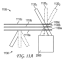
いくつかのディスプレイシステムでは、導波管のスタックを構成する、複数の導波管が、仮想画像を、ユーザから離れた異なる距離にあるように知覚される、複数の仮想深度平面(本明細書では、単に、「深度平面」とも称される)に形成するように構成され得る。いくつかの実施形態では、導波管のスタックの異なる導波管は、異なる屈折力を提供する、光学構造を有し得、ユーザの眼から異なる距離におけるオブジェクトから伝搬する光の波面発散をシミュレートし得る。いくつかの実施形態では、屈折力を提供するための導波管光学構造の代替として、またはそれに加え、ディスプレイシステムはまた、屈折力を提供する、または加えて提供する、複数のレンズを含んでもよい。画像源からの光は、導波管に向かって指向され得、各導波管の内部結合光学要素によって個々の導波管の中に内部結合され得る。内部結合光学要素は、格子等の回折光学要素であってもよい。 In some display systems, multiple waveguides that make up a stack of waveguides display a virtual image in multiple virtual depth planes (hereinafter referred to as (also simply referred to as a "depth plane"). In some embodiments, different waveguides in a stack of waveguides may have optical structures that provide different optical powers, simulating the wavefront divergence of light propagating from objects at different distances from the user's eye. It can be done. In some embodiments, as an alternative to, or in addition to, the waveguide optical structure to provide optical power, the display system may also include a plurality of lenses that provide, or in addition to, optical power. good. Light from the image source may be directed toward the waveguides and may be intercoupled into individual waveguides by the intercoupling optical elements of each waveguide. The internal coupling optical element may be a diffractive optical element such as a grating.
いくつかの実施形態では、本明細書に説明されるシステムおよび方法は、内部結合された光の再バウンスに起因した光損失の発生を低減させることによって、内部結合効率および/または内部結合された光の均一性を向上させるように構成される、内部結合光学要素を含む。再バウンスは、導波管に沿って伝搬する内部結合された光が、初期内部結合入射後、2回目または後続回数として、内部結合光学要素に衝打するときに生じる。より詳細に説明されるであろうように、再バウンスは、内部結合された光の一部が、望ましくないことに、内部結合光学要素の材料によって外部結合および/または吸収される結果をもたらし得る。外部結合および/または吸光は、望ましくないことに、全体的内部結合効率および/または内部結合された光の均一性の低減を生じさせ得る。 In some embodiments, the systems and methods described herein improve the intercoupling efficiency and/or the intercoupled light by reducing the occurrence of optical loss due to rebounce of the intercoupled light Includes an internal coupling optical element configured to improve light uniformity. Rebounce occurs when intercoupled light propagating along a waveguide strikes an incoupling optical element a second or subsequent time after the initial incoupling incidence. As will be explained in more detail, rebounce can result in a portion of the incoupled light being undesirably outcoupled and/or absorbed by the material of the incoupling optical element. . Outcoupling and/or absorption may undesirably result in a reduction in the overall incoupling efficiency and/or uniformity of the incoupled light.
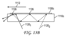
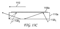
本明細書に開示されるいくつかの実施形態は、回折光学要素を提供し、これもまた、内部結合光学要素であって、導波管内で内部結合された光の再バウンスに起因する光損失を軽減させるように構成され得る。入射光を内部結合することに応じて、回折光学要素は、概して、導波管を通して伝搬方向に伝搬するように、光を再指向し得る。ある場合には、内部結合された光の再バウンスは、内部結合光学要素の側面に向かって伝搬方向に生じる。例えば、最初に、内部結合光学要素の反対(伝搬方向に対向する)側の近傍に内部結合された一部の入射光は、再バウンスし得る、すなわち、導波管の別の表面から反射後、再び、内部結合光学要素に衝打し得る。理論によって限定されるわけではないが、内部結合光学要素に衝打することに応じて、再び、入射光の一部は、望ましくないことに、光学要素によって外部結合され得、および/または光学要素によって吸収され得る(例えば、内部結合光学要素が反射性回折光学要素である場合、回折格子上の反射性コーティングによって吸収される)。 Some embodiments disclosed herein provide a diffractive optical element, which is also an internally coupled optical element, with optical loss due to rebounce of internally coupled light within the waveguide. may be configured to reduce In response to incoupling the incident light, the diffractive optical element can generally redirect the light to propagate in a propagation direction through the waveguide. In some cases, rebounce of the intercoupled light occurs in the direction of propagation toward the sides of the intercoupling optical element. For example, some incident light that is initially incoupled near the opposite (opposite the propagation direction) side of an incoupling optical element may rebounce, i.e., after reflection from another surface of the waveguide. , again may impact the internal coupling optical element. Without being limited by theory, in response to striking an in-coupling optical element, again, a portion of the incident light may be undesirably coupled out by the optical element and/or the optical element (e.g., by a reflective coating on the diffraction grating if the internal coupling optical element is a reflective diffractive optical element).
いくつかの実施形態では、再バウンスに起因する光損失を軽減させるために、内部結合光学要素は、光学要素の伝搬方向側において切頂される。有利なこととして、切頂は、再バウンスが望ましくない光損失をもたらす可能性が高い、内部結合光学要素の利用可能な面積を低減させることによって、再バウンスによって生じる光損失の発生を低減させ得る。いくつかの実施形態では、切頂は、内部結合光学要素の全ての構造の完全切頂であってもよく、例えば、切頂は、光伝搬の方向における内部結合光学要素の面積の低減を伴ってもよい。内部結合光学要素が反射性コーティング(例えば、金属層等の反射性層)を備える、いくつかの他の実施形態では、伝搬方向側における内部結合光学要素の一部は、伝搬方向側における光学要素の部分が、殆ど再バウンス光を吸収しない、および/またはより低い効率を伴って再バウンス光を外部結合するように、コーティングされなくてもよい。いくつかの実施形態では、上下図に見られるように、内部結合光学要素の回折領域は、伝搬方向に沿って、伝搬方向と垂直なその長さより短い幅を有してもよい、非切頂回折領域に対してより小さい幅対長さ比を有してもよい、および/または投影光学系からの光のビームの第1の部分が、回折領域上に入射し、光のビームの第2の部分が、回折領域上に入射せずに導波管上に衝突するように、サイズ決めおよび成形されてもよい(例えば、高吸収率および/または外部結合効率を有する光学要素の部分は、好ましくは、導波管上の光の入射ビームによって作り出される面積よりサイズが小さい)。いくつかの実施形態では、導波管のスタックにわたって、切頂の量は、導波管間で変動する。例えば、各導波管の内部結合光学要素の幅対長さ比は、導波管のスタックの異なる導波管間で変動し得る。 In some embodiments, the incoupling optical element is truncated on the propagation direction side of the optical element to reduce optical loss due to rebounce. Advantageously, truncations may reduce the occurrence of light loss caused by rebounce by reducing the available area of the internal coupling optical element, where rebounce is likely to result in undesirable light loss. . In some embodiments, the truncation may be a complete truncation of all structures of the intercoupling optical element, e.g., the truncation involves a reduction in the area of the intercoupling optical element in the direction of light propagation. You can. In some other embodiments, where the incoupling optical element comprises a reflective coating (e.g., a reflective layer such as a metal layer), a portion of the incoupling optical element on the direction of propagation side is less than or equal to the optical element on the direction of propagation side. may be uncoated so that it absorbs little rebounced light and/or couples out rebounced light with lower efficiency. In some embodiments, the diffractive region of the internal coupling optical element may have a width along the propagation direction that is less than its length perpendicular to the propagation direction, as seen in the top and bottom views. may have a smaller width-to-length ratio for the diffractive region and/or a first portion of the beam of light from the projection optics is incident on the diffractive region and a second portion of the beam of light may be sized and shaped such that a portion of the optical element with high absorption and/or outcoupling efficiency impinges on the waveguide without incident on the diffractive region (e.g., a portion of the optical element with high absorption and/or outcoupling efficiency is (preferably smaller in size than the area created by the incident beam of light on the waveguide). In some embodiments, across a stack of waveguides, the amount of truncation varies from waveguide to waveguide. For example, the width-to-length ratio of the internal coupling optical elements of each waveguide may vary between different waveguides of a stack of waveguides.
導波管は、光学要素を使用して、外部光を内部結合し、および/または導波管内を伝搬する光を所望の方向に再指向してもよい。例えば、光学要素は、回折格子および/またはファセット特徴の形態をとってもよい。いくつかの光学要素は、反射性モードで作用してもよく、光学要素上に1つ以上の角度から入射する光は、異なる所望の角度で光学要素から離れるように伝搬するように、反射および再指向の両方を行う。本明細書に開示されるように、そのような導波管は、拡張現実および仮想現実ディスプレイシステム等のディスプレイシステムの一部を形成してもよい。例えば、導波管は、画像情報を含有する光を内部結合し、その光をユーザに分散および外部結合するように構成されてもよい。例示的導波管および光学要素は、本明細書でより詳細に議論されるであろう。反射性光学要素は、湿式化学作用によって形成される反射性層を含んでもよく、これは、有利なこととして、本明細書に議論されるように、より優れた回折効率を提供し得る。 The waveguide may use optical elements to internally couple external light and/or redirect light propagating within the waveguide in a desired direction. For example, the optical elements may take the form of diffraction gratings and/or facet features. Some optical elements may operate in a reflective mode, such that light incident on the optical element from one or more angles is reflected and propagated away from the optical element at different desired angles. Do both reorientation. As disclosed herein, such waveguides may form part of display systems such as augmented reality and virtual reality display systems. For example, a waveguide may be configured to incouple light containing image information and disperse and outcouple the light to a user. Exemplary waveguides and optical elements will be discussed in more detail herein. The reflective optical element may include a reflective layer formed by wet chemistry, which may advantageously provide greater diffraction efficiency, as discussed herein.
ここで、同様の参照番号が全体を通して同様の部分を指す、図面を参照する。別様に示されない限り、図面は、概略であって、必ずしも、正確な縮尺で描かれていない。 Reference is now made to the drawings, in which like reference numbers refer to like parts throughout. Unless otherwise indicated, the drawings are schematic and not necessarily drawn to scale.
例示的ディスプレイシステム
図2は、ユーザのための3次元画像をシミュレートするための従来のディスプレイシステムを図示する。ユーザの眼は、離間されており、空間内の実オブジェクトを見ているとき、各眼は、オブジェクトの若干異なるビューを有し、オブジェクトの画像を各眼の網膜上の異なる場所に形成し得ることを理解されたい。これは、両眼視差と称され得、ヒト視覚系によって、深度の知覚を提供するために利用され得る。従来のディスプレイシステムは、仮想オブジェクトが所望の深度における実オブジェクトであるように各眼によって見えるであろう仮想オブジェクトのビューに対応する、眼210、220毎に1つの同一仮想オブジェクトの若干異なるビューを伴う2つの明確に異なる画像190、200を提示することによって、両眼視差をシミュレートする。これらの画像は、ユーザの視覚系が深度の知覚を導出するために解釈する、両眼キューを提供する。
Exemplary Display System FIG. 2 illustrates a conventional display system for simulating three-dimensional images for a user. The user's eyes are spaced apart, and when viewing a real object in space, each eye may have a slightly different view of the object and form an image of the object at a different location on each eye's retina. I hope you understand that. This may be referred to as binocular disparity and may be exploited by the human visual system to provide depth perception. Conventional display systems provide slightly different views of the same virtual object for each
図2を継続して参照すると、画像190、200は、z-軸上で距離230だけ眼210、220から離間される。z-軸は、その眼が視認者の直前の光学無限遠におけるオブジェクトを凝視している状態の視認者の光学軸と平行である。画像190、200は、平坦であって、眼210、220から固定距離にある。それぞれ、眼210、220に提示される画像内の仮想オブジェクトの若干異なるビューに基づいて、眼は、必然的に、オブジェクトの画像が眼のそれぞれの網膜上の対応する点に来て、単一両眼視を維持するように回転し得る。本回転は、眼210、220のそれぞれの視線を仮想オブジェクトが存在するように知覚される空間内の点上に収束させ得る。その結果、3次元画像の提供は、従来、ユーザの眼210、220の輻輳・開散運動を操作し得、ヒト視覚系が深度の知覚を提供するように解釈する、両眼キューを提供することを伴う。
With continued reference to FIG. 2,
しかしながら、深度の現実的かつ快適な知覚の生成は、困難である。眼からの異なる距離におけるオブジェクトからの光は、異なる発散量を伴う波面を有することを理解されたい。図3A-3Cは、距離と光線の発散との間の関係を図示する。オブジェクトと眼210との間の距離は、減少距離R1、R2、およびR3の順序で表される。図3A-3Cに示されるように、光線は、オブジェクトまでの距離が減少するにつれてより発散する。逆に言えば、距離が増加するにつれて、光線は、よりコリメートされる。換言すると、点(オブジェクトまたはオブジェクトの一部)によって生成されるライトフィールドは、点がユーザの眼から離れている距離の関数である、球状波面曲率を有すると言え得る。曲率は、オブジェクトと眼210との間の距離が減少するにつれて増加する。単眼210のみが、例証を明確にするために、図3A-3Cおよび本明細書の種々の他の図に図示されるが、眼210に関する議論は、視認者の両眼210および220に適用され得る。
However, generating a realistic and comfortable perception of depth is difficult. It should be understood that light from an object at different distances from the eye has wavefronts with different amounts of divergence. 3A-3C illustrate the relationship between distance and ray divergence. The distances between the object and the
図3A-3Cを継続して参照すると、視認者の眼が凝視しているオブジェクトからの光は、異なる波面発散度を有し得る。異なる波面発散量に起因して、光は、眼の水晶体によって異なるように集束され得、これは、ひいては、水晶体に、異なる形状をとり、集束された画像を眼の網膜上に形成することを要求し得る。集束された画像が、網膜上に形成されない場合、結果として生じる網膜ぼけは、集束された画像が網膜上に形成されるまで、眼の水晶体の形状に変化を生じさせる、遠近調節のためのキューとして作用する。例えば、遠近調節のためのキューは、眼の水晶体を囲繞する毛様筋の弛緩または収縮をトリガし、それによって、レンズを保持する低靱帯に印加される力を変調し、したがって、固視しているオブジェクトの網膜ぼけが排除または最小限にされるまで、眼の水晶体の形状を変化させ、それによって、凝視されているオブジェクトの集束された画像を眼の網膜(例えば、中心窩)上に形成し得る。眼の水晶体が形状を変化させるプロセスは、遠近調節と称され得、凝視されているオブジェクトの集束された画像を眼の網膜(例えば、中心窩)上に形成するために要求される眼の水晶体の形状は、遠近調節状態と称され得る。 With continued reference to FIGS. 3A-3C, the light from the object that the viewer's eyes are fixating on may have different wavefront emittances. Due to different amounts of wavefront divergence, light may be focused differently by the eye's lens, which in turn causes the lens to take different shapes and form a focused image on the eye's retina. can be requested. If a focused image is not formed on the retina, the resulting retinal blur is a cue for accommodation that causes a change in the shape of the eye's lens until a focused image is formed on the retina. It acts as. For example, cues for accommodation trigger relaxation or contraction of the ciliary muscles surrounding the eye's crystalline lens, thereby modulating the force applied to the lower ligament that holds the lens and, therefore, fixation. changes the shape of the lens of the eye, thereby depositing a focused image of the object being gazed onto the retina of the eye (e.g., the fovea) until retinal blur of the object being gazed at is eliminated or minimized. can be formed. The process by which the eye's lens changes shape can be referred to as accommodation, and the eye's lens is required to form a focused image of the object being gazed on the eye's retina (e.g., fovea). The shape of can be referred to as an accommodative state.
ここで図4Aを参照すると、ヒト視覚系の遠近調節-輻輳・開散運動応答の表現が、図示される。オブジェクトを凝視するための眼の移動は、眼にオブジェクトからの光を受光させ、光は、画像を眼の網膜のそれぞれ上に形成する。網膜上に形成される画像内の網膜ぼけの存在は、遠近調節のためのキューを提供し得、網膜上の画像の相対的場所は、輻輳・開散運動のためのキューを提供し得る。遠近調節するためのキューは、遠近調節を生じさせ、眼の水晶体がオブジェクトの集束された画像を眼の網膜(例えば、中心窩)上に形成する特定の遠近調節状態をとる結果をもたらす。一方、輻輳・開散運動のためのキューは、各眼の各網膜上に形成される画像が単一両眼視を維持する対応する網膜点にあるように、輻輳・開散運動移動(眼の回転)を生じさせる。これらの位置では、眼は、特定の輻輳・開散運動状態をとっていると言え得る。図4Aを継続して参照すると、遠近調節は、眼が特定の遠近調節状態を達成するプロセスであると理解され得、輻輳・開散運動は、眼が特定の輻輳・開散運動状態を達成するプロセスであると理解され得る。図4Aに示されるように、眼の遠近調節および輻輳・開散運動状態は、ユーザが別のオブジェクトを凝視する場合、変化し得る。例えば、遠近調節された状態は、ユーザがz-軸上の異なる深度における新しいオブジェクトを凝視する場合、変化し得る。 Referring now to FIG. 4A, a representation of the accommodation-convergence-divergence motion response of the human visual system is illustrated. Movement of the eyes to gaze at an object causes the eyes to receive light from the object, which forms an image on each of the eye's retinas. The presence of retinal blur within the image formed on the retina may provide a cue for accommodation, and the relative location of the image on the retina may provide a cue for convergence-divergent motion. Cues to accommodate cause accommodation and result in the lens of the eye assuming a particular accommodative state that forms a focused image of the object on the retina (eg, fovea) of the eye. On the other hand, the cues for convergence-divergent motion (ocular divergence motion) are such that the images formed on each retina of each eye are at the corresponding retinal points maintaining single binocular vision. rotation). In these positions, the eye can be said to be in a particular state of convergence and divergence motion. With continued reference to FIG. 4A, accommodation can be understood to be the process by which the eye achieves a particular state of accommodation, and convergence-divergence motion refers to the process by which the eye achieves a particular state of convergence-divergence motion. It can be understood as a process of As shown in FIG. 4A, the accommodation and convergence/divergence motion state of the eye may change when the user gazes at another object. For example, the accommodated state may change if the user gazes at a new object at a different depth on the z-axis.
理論によって限定されるわけではないが、オブジェクトの視認者は、輻輳・開散運動および遠近調節の組み合わせに起因して、オブジェクトを「3次元」であると知覚し得ると考えられる。前述のように、2つの眼の相互に対する輻輳・開散運動移動(例えば、瞳孔が相互に向かって、またはそこから移動し、眼の視線を収束させ、オブジェクトを凝視するような眼の回転)は、眼の水晶体の遠近調節と密接に関連付けられる。通常条件下では、眼の水晶体の形状を変化させ、1つのオブジェクトから異なる距離における別のオブジェクトに焦点を変化させることは、自動的に、「遠近調節-輻輳・開散運動反射」として知られる関係下、同一距離まで輻輳・開散運動における整合する変化を生じさせるであろう。同様に、輻輳・開散運動における変化は、通常条件下、水晶体形状における整合する変化をトリガするであろう。 Without being limited by theory, it is believed that a viewer of an object may perceive the object to be "three-dimensional" due to a combination of convergence-divergent motion and accommodation. As mentioned above, convergence-divergence movement of the two eyes relative to each other (e.g., rotation of the eyes such that the pupils move toward or away from each other, converging the lines of sight of the eyes, and gazing at an object) is closely associated with the accommodation of the crystalline lens of the eye. Under normal conditions, changing the shape of the lens of the eye and changing its focus from one object to another at different distances is automatically known as the "accommodation-convergence-divergence motor reflex." under the relationship, up to the same distance will produce matching changes in the convergence-divergence motion. Similarly, changes in convergence-divergence motion will, under normal conditions, trigger matching changes in lens shape.
ここで図4Bを参照すると、眼の異なる遠近調節および輻輳・開散運動状態の実施例が、図示される。対の眼222aは、光学無限遠におけるオブジェクトを凝視する一方、対の眼222bは、光学無限遠未満におけるオブジェクト221を凝視する。着目すべきこととして、各対の眼の輻輳・開散運動状態は、異なり、対の眼222aは、まっすぐ指向される一方、対の眼222は、オブジェクト221上に収束する。各対の眼222aおよび222bを形成する眼の遠近調節状態もまた、水晶体210a、220aの異なる形状によって表されるように異なる。 Referring now to FIG. 4B, examples of different accommodative and convergence/divergent motion states of the eye are illustrated. Paired eye 222a gazes at an object at optical infinity, while paired eye 222b gazes at object 221 at less than optical infinity. It should be noted that the convergence/divergence motion state of each pair of eyes is different, with pair of eyes 222 a being directed straight, while pair of eyes 222 converging on object 221 . The accommodation conditions of the eyes forming each pair of eyes 222a and 222b are also different, as represented by the different shapes of the lenses 210a, 220a.
望ましくないことに、従来の「3-D」ディスプレイシステムの多くのユーザは、これらのディスプレイにおける遠近調節と輻輳・開散運動状態との間の不整合に起因して、そのような従来のシステムを不快であると見出す、または奥行感を全く知覚しない場合がある。前述のように、多くの立体視または「3-D」ディスプレイシステムは、若干異なる画像を各眼に提供することによって、場面を表示する。そのようなシステムは、それらが、とりわけ、単に、場面の異なる提示を提供し、眼の輻輳・開散運動状態に変化を生じさせるが、それらの眼の遠近調節状態に対応する変化を伴わないため、多くの視認者にとって不快である。むしろ、画像は、眼が全ての画像情報を単一遠近調節状態において視認するように、ディスプレイによって眼から固定距離に示される。そのような配列は、遠近調節状態における整合する変化を伴わずに輻輳・開散運動状態に変化を生じさせることによって、「遠近調節-輻輳・開散運動反射」に逆らう。本不整合は、視認者不快感を生じさせると考えられる。遠近調節と輻輳・開散運動との間のより良好な整合を提供する、ディスプレイシステムは、3次元画像のより現実的かつ快適なシミュレーションを形成し得る。 Undesirably, many users of conventional "3-D" display systems find that due to the mismatch between accommodation and convergent/divergent motion states in these displays, may find it unpleasant or may not perceive a sense of depth at all. As mentioned above, many stereoscopic or "3-D" display systems display a scene by providing a slightly different image to each eye. Such systems require that they, inter alia, merely provide different presentations of the scene and cause changes in the convergence-divergent motion state of the eyes, but without corresponding changes in the accommodative state of those eyes. Therefore, it is uncomfortable for many viewers. Rather, the image is presented by the display at a fixed distance from the eye such that the eye views all image information in a single state of accommodation. Such an arrangement counters the "accommodation-convergence-divergence motion reflex" by producing a change in the convergence-divergence motion state without a corresponding change in the accommodation state. This inconsistency is considered to cause viewer discomfort. A display system that provides a better match between accommodation and convergence-divergent motion may create a more realistic and comfortable simulation of three-dimensional images.
理論によって限定されるわけではないが、ヒトの眼は、典型的には、有限数の深度平面を解釈し、深度知覚を提供することができると考えられる。その結果、知覚された深度の高度に真実味のあるシミュレーションが、眼にこれらの限定数の深度平面のそれぞれに対応する画像の異なる提示を提供することによって達成され得る。いくつかの実施形態では、異なる提示は、輻輳・開散運動のためのキューおよび遠近調節するための整合するキューの両方を提供し、それによって、生理学的に正しい遠近調節-輻輳・開散運動整合を提供してもよい。 Without being limited by theory, it is believed that the human eye typically interprets a finite number of depth planes and is capable of providing depth perception. As a result, a highly realistic simulation of perceived depth can be achieved by providing the eye with different presentations of images corresponding to each of these limited number of depth planes. In some embodiments, the different presentations provide both cues for convergence-divergent motion and matching cues for accommodation, thereby providing physiologically correct accommodation-convergence-divergent motion. May provide alignment.
図4Bを継続して参照すると、眼210、220からの空間内の異なる距離に対応する、2つの深度平面240が、図示される。所与の深度平面240に関して、輻輳・開散運動キューが、眼210、220毎に適切に異なる視点の画像を表示することによって提供されてもよい。加えて、所与の深度平面240に関して、各眼210、220に提供される画像を形成する光は、その深度平面240の距離におけるある点によって生成されたライトフィールドに対応する波面発散を有してもよい。
With continued reference to FIG. 4B, two
図示される実施形態では、点221を含有する、深度平面240のz-軸に沿った距離は、1mである。本明細書で使用されるように、z-軸に沿った距離または深度は、ユーザの眼の射出瞳に位置するゼロ点を用いて測定されてもよい。したがって、1mの深度に位置する深度平面240は、眼が光学無限遠に向かって指向された状態での、それらの眼の光学軸上のユーザの眼の射出瞳から1m離れた距離に対応する。近似値として、z-軸に沿った深度または距離は、ユーザの眼の正面のディスプレイ(例えば、導波管の表面)から測定され、デバイスとユーザの眼の射出瞳との間の距離に関する値が加えられてもよい。その値は、瞳距離と呼ばれ、ユーザの眼の射出瞳と眼の正面のユーザによって装着されるディスプレイとの間の距離に対応し得る。実際は、瞳距離に関する値は、概して、全ての視認者に関して使用される、正規化された値であってもよい。例えば、瞳距離は、20mmであると仮定され得、1mの深度における深度平面は、ディスプレイの正面の980mmの距離にあり得る。
In the illustrated embodiment, the distance along the z-axis of
ここで図4Cおよび4Dを参照すると、整合遠近調節-輻輳・開散運動距離および不整合遠近調節-輻輳・開散運動距離の実施例が、それぞれ、図示される。図4Cに図示されるように、ディスプレイシステムは、仮想オブジェクトの画像を各眼210、220に提供してもよい。画像は、眼210、220に、眼が深度平面240上の点15上に収束する、輻輳・開散運動状態をとらせ得る。加えて、画像は、その深度平面240における実オブジェクトに対応する波面曲率を有する光によって形成され得る。その結果、眼210、220は、画像がそれらの眼の網膜上に合焦する、遠近調節状態をとる。したがって、ユーザは、仮想オブジェクトを深度平面240上の点15にあるように知覚し得る。
Referring now to FIGS. 4C and 4D, examples of matched accommodation-convergence-divergence motion distances and mismatched accommodation-convergence-divergence motion distances are illustrated, respectively. As illustrated in FIG. 4C, the display system may provide images of virtual objects to each
眼210、220の遠近調節および輻輳・開散運動状態はそれぞれ、z-軸上の特定の距離と関連付けられることを理解されたい。例えば、眼210、220からの特定の距離におけるオブジェクトは、それらの眼に、オブジェクトの距離に基づいて、特定の遠近調節状態をとらせる。特定の遠近調節状態と関連付けられた距離は、遠近調節距離Adと称され得る。同様に、特定の輻輳・開散運動状態における眼と関連付けられた特定の輻輳・開散運動距離Vdまたは相互に対する位置が、存在する。遠近調節距離および輻輳・開散運動距離が整合する場合、遠近調節と輻輳・開散運動との間の関係は、生理学に正しいと言える。これは、視認者に最も快適なシナリオであると見なされる。
It should be appreciated that the accommodation and convergence/divergence motion states of the
しかしながら、立体視ディスプレイでは、遠近調節距離および輻輳・開散運動距離は、常時、整合しない場合がある。例えば、図4Dに図示されるように、眼210、220に表示される画像は、深度平面240に対応する波面発散を伴って表示され得、眼210、220は、その深度平面上の点15a、15bが合焦する、特定の遠近調節状態をとり得る。しかしながら、眼210、220に表示される画像は、眼210、220を深度平面240上に位置しない点15上に収束させる、輻輳・開散運動のためのキューを提供し得る。その結果、遠近調節距離は、いくつかの実施形態では、眼210、220の射出瞳から深度平面240の距離に対応する一方、輻輳・開散運動距離は、眼210、220の射出瞳から点15までのより大きい距離に対応する。遠近調節距離は、輻輳・開散運動距離と異なる。その結果、遠近調節-輻輳・開散運動不整合が存在する。そのような不整合は、望ましくないと見なされ、不快感をユーザに生じさせ得る。不整合は、距離(例えば、Vd-Ad)に対応し、ジオプタを使用して特性評価され得ることを理解されたい。
However, in stereoscopic displays, the accommodative distance and the convergence/divergent motion distance may not always align. For example, as illustrated in FIG. 4D, the image displayed to the
いくつかの実施形態では、同一参照点が遠近調節距離および輻輳・開散運動距離のために利用される限り、眼210、220の射出瞳以外の参照点が、遠近調節距離および輻輳・開散運動不整合を決定するための距離を決定するために利用されてもよいことを理解されたい。例えば、距離は、角膜から深度平面まで、網膜から深度平面、接眼レンズ(例えば、ディスプレイデバイスの導波管)から深度平面まで等で測定され得る。
In some embodiments, a reference point other than the exit pupil of the
理論によって限定されるわけではないが、ユーザは、依然として、不整合自体が有意な不快感を生じさせずに、生理学的に正しい最大0.25ジオプタ、最大0.33ジオプタ、および最大約0.5ジオプタの遠近調節-輻輳・開散運動不整合を知覚し得ると考えられる。いくつかの実施形態では、本明細書に開示されるディスプレイシステム(例えば、ディスプレイシステム250、図6)は、0.5ジオプタまたはそれ未満の遠近調節-輻輳・開散運動不整合を有する画像を視認者に提示する。いくつかの他の実施形態では、ディスプレイシステムによって提供される画像の遠近調節-輻輳・開散運動不整合は、約0.33ジオプタまたはそれ未満である。さらに他の実施形態では、ディスプレイシステムによって提供される画像の遠近調節-輻輳・開散運動不整合は、約0.1ジオプタまたはそれ未満を含む、0.25ジオプタまたはそれ未満である。 Without being limited by theory, users can still achieve physiologically correct up to 0.25 diopters, up to 0.33 diopters, and up to about 0.25 diopters without the misalignment itself causing significant discomfort. It is believed that an accommodation-convergence-divergence motion mismatch of 5 diopters can be perceived. In some embodiments, the display systems disclosed herein (e.g., display system 250, FIG. 6) display images having an accommodation-convergence-divergence motion mismatch of 0.5 diopters or less. Present to the viewer. In some other embodiments, the accommodation-convergence-divergence motion misalignment of the image provided by the display system is about 0.33 diopters or less. In yet other embodiments, the accommodation-convergence-divergence motion misalignment of the images provided by the display system is 0.25 diopters or less, including about 0.1 diopters or less.
図5は、波面発散を修正することによって、3次元画像をシミュレートするためのアプローチの側面を図示する。ディスプレイシステムは、画像情報でエンコードされた光770を受光し、その光をユーザの眼210に出力するように構成される、導波管270を含む。導波管270は、所望の深度平面240上のある点によって生成されたライトフィールドの波面発散に対応する定義された波面発散量を伴って光650を出力してもよい。いくつかの実施形態では、同一量の波面発散が、その深度平面上に提示される全てのオブジェクトのために提供される。加えて、ユーザの他方の眼は、類似導波管からの画像情報を提供され得るように図示されるであろう。
FIG. 5 illustrates aspects of an approach for simulating three-dimensional images by modifying wavefront divergence. The display system includes a
いくつかの実施形態では、単一導波管が、単一または限定数の深度平面に対応する設定された波面発散量を伴う光を出力するように構成されてもよく、および/または導波管は、限定された範囲の波長の光を出力するように構成されてもよい。その結果、いくつかの実施形態では、複数またはスタックの導波管が、異なる深度平面のための異なる波面発散量を提供し、および/または異なる範囲の波長の光を出力するために利用されてもよい。本明細書で使用されるように、深度平面は、平面であってもよい、または湾曲表面の輪郭に追従してもよいことを理解されるであろう。スタックの1つ以上の導波管は、本明細書に説明されるように、純または実質的に純金属を含む、それから本質的に成る、またはそれから成る、反射性層を備える、反射性回折光学要素を備えてもよい。 In some embodiments, a single waveguide may be configured to output light with a set wavefront divergence corresponding to a single or limited number of depth planes, and/or the waveguide The tube may be configured to output light in a limited range of wavelengths. As a result, in some embodiments, multiple or stacked waveguides are utilized to provide different amounts of wavefront divergence for different depth planes and/or to output light at different ranges of wavelengths. Good too. It will be appreciated that, as used herein, a depth plane may be a plane or may follow the contour of a curved surface. One or more of the waveguides of the stack comprises a reflective layer comprising, consisting essentially of, or consisting of a pure or substantially pure metal, as described herein. Optical elements may also be provided.
図6は、画像情報をユーザに出力するための導波管スタックの実施例を図示する。ディスプレイシステム250は、複数の導波管270、280、290、300、310を使用して3次元知覚を眼/脳に提供するために利用され得る、導波管のスタックまたはスタックされた導波管アセンブリ260を含む。ディスプレイシステム250は、いくつかの実施形態では、ライトフィールドディスプレイと見なされてもよいことを理解されたい。加えて、導波管アセンブリ260はまた、接眼レンズとも称され得る。
FIG. 6 illustrates an example of a waveguide stack for outputting image information to a user. The display system 250 may be utilized to provide a three-dimensional perception to the eye/brain using a plurality of
いくつかの実施形態では、ディスプレイシステム250は、輻輳・開散運動するための実質的に連続キューおよび遠近調節するための複数の離散キューを提供するように構成されてもよい。輻輳・開散運動のためのキューは、異なる画像をユーザの眼のそれぞれに表示することによって提供されてもよく、遠近調節のためのキューは、選択可能離散量の波面発散を伴う画像を形成する光を出力することによって提供されてもよい。換言すると、ディスプレイシステム250は、可変レベルの波面発散を伴う光を出力するように構成されてもよい。いくつかの実施形態では、波面発散の各離散レベルは、特定の深度平面に対応し、導波管270、280、290、300、310のうちの特定の1つによって提供されてもよい。
In some embodiments, display system 250 may be configured to provide a substantially continuous cue for convergence and divergence motion and a plurality of discrete cues for accommodation. Cues for convergence and divergence motion may be provided by displaying different images to each of the user's eyes, and cues for accommodation form images with selectable discrete amounts of wavefront divergence. It may also be provided by outputting light that In other words, display system 250 may be configured to output light with variable levels of wavefront divergence. In some embodiments, each discrete level of wavefront divergence corresponds to a particular depth plane and may be provided by a particular one of
図6を継続して参照すると、導波管アセンブリ260はまた、複数の特徴320、330、340、350を導波管間に含んでもよい。いくつかの実施形態では、特徴320、330、340、350は、1つ以上のレンズであってもよい。導波管270、280、290、300、310および/または複数のレンズ320、330、340、350は、種々のレベルの波面曲率または光線発散を用いて画像情報を眼に送信するように構成されてもよい。各導波管レベルは、特定の深度平面と関連付けられてもよく、その深度平面に対応する画像情報を出力するように構成されてもよい。画像投入デバイス360、370、380、390、400は、導波管のための光源として機能してもよく、画像情報を導波管270、280、290、300、310の中に投入するために利用されてもよく、それぞれ、本明細書に説明されるように、眼210に向かって出力のために各個別の導波管を横断して入射光を分散させるように構成されてもよい。光は、画像投入デバイス360、370、380、390、400の出力表面410、420、430、440、450から出射し、導波管270、280、290、300、310の対応する入力表面460、470、480、490、500の中に投入される。いくつかの実施形態では、入力表面460、470、480、490、500はそれぞれ、対応する導波管の縁であってもよい、または対応する導波管の主要表面の一部(すなわち、世界510または視認者の眼210に直接面する導波管表面のうちの1つ)であってもよい。いくつかの実施形態では、光の単一ビーム(例えば、コリメートされたビーム)が、各導波管の中に投入され、クローン化されたコリメートビームの全体場を出力してもよく、これは、特定の導波管と関連付けられた深度平面に対応する特定の角度(および発散量)において眼210に向かって指向される。いくつかの実施形態では、画像投入デバイス360、370、380、390、400のうちの単一の1つは、複数(例えば、3つ)の導波管270、280、290、300、310と関連付けられ、その中に光を投入してもよい。
With continued reference to FIG. 6, waveguide assembly 260 may also include a plurality of features 320, 330, 340, 350 between the waveguides. In some embodiments, features 320, 330, 340, 350 may be one or more lenses. The
いくつかの実施形態では、画像投入デバイス360、370、380、390、400はそれぞれ、それぞれ対応する導波管270、280、290、300、310の中への投入のために画像情報を生成する、離散ディスプレイである。いくつかの他の実施形態では、画像投入デバイス360、370、380、390、400は、例えば、画像情報を1つ以上の光学導管(光ファイバケーブル等)を介して画像投入デバイス360、370、380、390、400のそれぞれに送り得る、単一の多重化されたディスプレイの出力端である。画像投入デバイス360、370、380、390、400によって提供される画像情報は、異なる波長または色(例えば、本明細書に議論されるように、異なる原色)の光を含んでもよいことを理解されたい。
In some embodiments, each image injection device 360, 370, 380, 390, 400 generates image information for injection into a
いくつかの実施形態では、導波管270、280、290、300、310の中に投入される光は、光プロジェクタシステム520によって提供され、これは、光モジュール530を備え、これは、発光ダイオード(LED)等の光エミッタを含んでもよい。光モジュール530からの光は、ビームスプリッタ550を介して、光変調器540、例えば、空間光変調器によって指向および修正されてもよい。光変調器540は、導波管270、280、290、300、310の中に投入される光の知覚される強度を変化させ、光を画像情報でエンコードするように構成されてもよい。空間光変調器の実施例は、液晶ディスプレイ(LCD)を含み、シリコン上液晶(LCOS)ディスプレイを含む。画像投入デバイス360、370、380、390、400は、図式的に図示され、いくつかの実施形態では、これらの画像投入デバイスは、光を導波管270、280、290、300、310の関連付けられたものの中に出力するように構成される、共通投影システム内の異なる光経路および場所を表し得ることを理解されたい。いくつかの実施形態では、導波管アセンブリ260の導波管は、導波管の中に投入された光をユーザの眼に中継しながら、理想的レンズとして機能し得る。本概念では、オブジェクトは、空間光変調器540であってもよく、画像は、深度平面上の画像であってもよい。
In some embodiments, the light injected into the
いくつかの実施形態では、ディスプレイシステム250は、光を種々のパターン(例えば、ラスタ走査、螺旋走査、リサジューパターン等)で1つ以上の導波管270、280、290、300、310の中に、最終的には、視認者の眼210に投影するように構成される、1つ以上の走査ファイバを備える、走査ファイバディスプレイであってもよい。いくつかの実施形態では、図示される画像投入デバイス360、370、380、390、400は、光を1つまたは複数の導波管270、280、290、300、310の中に投入するように構成される、単一走査ファイバまたは走査ファイバの束を図式的に表し得る。いくつかの他の実施形態では、図示される画像投入デバイス360、370、380、390、400は、複数の走査ファイバまたは走査ファイバの複数の束を図式的に表し得、それぞれ、光を導波管270、280、290、300、310のうちの関連付けられた1つの中に投入するように構成される。1つ以上の光ファイバは、光を光モジュール530から1つ以上の導波管270、280、290、300、310に透過するように構成されてもよいことを理解されたい。1つ以上の介在光学構造が、走査ファイバまたは複数のファイバと、1つ以上の導波管270、280、290、300、310との間に提供され、例えば、走査ファイバから出射する光を1つ以上の導波管270、280、290、300、310の中に再指向してもよいことを理解されたい。
In some embodiments, display system 250 transmits light into one or
コントローラ560は、画像投入デバイス360、370、380、390、400、光源530、および光変調器540の動作を含む、スタックされた導波管アセンブリ260のうちの1つ以上のものの動作を制御する。いくつかの実施形態では、コントローラ560は、ローカルデータ処理モジュール140の一部である。コントローラ560は、例えば、本明細書に開示される種々のスキームのいずれかに従って、導波管270、280、290、300、310への画像情報のタイミングおよびプロビジョニングを調整する、プログラミング(例えば、非一過性媒体内の命令)を含む。いくつかの実施形態では、コントローラは、単一一体型デバイスまたは有線または無線通信チャネルによって接続される分散型システムであってもよい。コントローラ560は、いくつかの実施形態では、処理モジュール140または150(図9D)の一部であってもよい。 Controller 560 controls operation of one or more of stacked waveguide assemblies 260, including operation of image injection devices 360, 370, 380, 390, 400, light source 530, and light modulator 540. . In some embodiments, controller 560 is part of local data processing module 140. Controller 560 may be configured to program (e.g., instructions in ephemeral media). In some embodiments, the controller may be a single integrated device or a distributed system connected by wired or wireless communication channels. Controller 560 may be part of processing module 140 or 150 (FIG. 9D) in some embodiments.
図6を継続して参照すると、導波管270、280、290、300、310は、全内部反射(TIR)によって各個別の導波管内で光を伝搬するように構成されてもよい。導波管270、280、290、300、310はそれぞれ、主要な上部および底部表面およびそれらの主要上部表面と底部表面との間に延在する縁を伴う、平面である、または別の形状(例えば、湾曲)を有してもよい。図示される構成では、導波管270、280、290、300、310はそれぞれ、各個別の導波管内で伝搬する光を導波管から再指向し、画像情報を眼210に出力することによって、光を導波管から抽出するように構成される、外部結合光学要素570、580、590、600、610を含んでもよい。抽出された光はまた、外部結合光と称され得、外部結合光学要素はまた、光抽出光学要素と称され得る。抽出された光のビームは、導波管によって、導波管内を伝搬する光が光抽出光学要素に衝打する場所において出力され得る。外部結合光学要素570、580、590、600、610は、例えば、本明細書にさらに議論されるような回折光学特徴を含む、格子であってもよい。説明の容易性および図面の明確性のために、導波管270、280、290、300、310の底部主要表面に配置されて図示されるが、いくつかの実施形態では、外部結合光学要素570、580、590、600、610は、本明細書にさらに議論されるように、上部および/または底部主要表面に配置されてもよい、および/または導波管270、280、290、300、310の体積内に直接配置されてもよい。いくつかの実施形態では、外部結合光学要素570、580、590、600、610は、透明基板に取り付けられ、導波管270、280、290、300、310を形成する、材料の層内に形成されてもよい。いくつかの他の実施形態では、導波管270、280、290、300、310は、材料のモノリシック部品であってもよく、外部結合光学要素570、580、590、600、610は、材料のその部品の表面上および/またはその内部に形成されてもよい。
With continued reference to FIG. 6,
図6を継続して参照すると、本明細書に議論されるように、各導波管270、280、290、300、310は、光を出力し、特定の深度平面に対応する画像を形成するように構成される。例えば、眼の最近傍の導波管270は、眼210にコリメートされた光(そのような導波管270の中に投入された)を送達するように構成されてもよい。コリメートされた光は、光学無限遠焦点面を表し得る。次の上方の導波管280は、眼210に到達し得る前に、第1のレンズ350(例えば、負のレンズ)を通して通過する、コリメートされた光を送出するように構成されてもよい。そのような第1のレンズ350は、眼/脳が、その次の上方の導波管280から生じる光を光学無限遠から眼210に向かって内向きにより近い第1の焦点面から生じるように解釈するように、若干の凸面波面曲率を生成するように構成されてもよい。同様に、第3の上方の導波管290は、眼210に到達する前に、その出力光を第1のレンズ350および第2のレンズ340の両方を通して通過させる。第1のレンズ350および第2のレンズ340の組み合わせられた屈折力は、眼/脳が、第3の導波管290から生じる光が次の上方の導波管280からの光であったよりも光学無限遠から人物に向かって内向きにさらに近い第2の焦点面から生じるように解釈するように、別の漸増量の波面曲率を生成するように構成されてもよい。
With continued reference to FIG. 6, each
他の導波管層300、310およびレンズ330、320も同様に構成され、スタック内の最高導波管310は、人物に最も近い焦点面を表す集約焦点力のために、その出力をそれと眼との間のレンズの全てを通して送出する。スタックされた導波管アセンブリ260の他側の世界510から生じる光を視認/解釈するとき、レンズ320、330、340、350のスタックを補償するために、補償レンズ層620が、スタックの上部に配置され、下方のレンズスタック320、330、340、350の集約力を補償してもよい。そのような構成は、利用可能な導波管/レンズ対と同じ数の知覚される焦点面を提供する。導波管の外部結合光学要素およびレンズの集束側面は両方とも、静的であってもよい(すなわち、動的または電気活性ではない)。いくつかの代替実施形態では、一方または両方とも、電気活性特徴を使用して動的であってもよい。 The other waveguide layers 300, 310 and lenses 330, 320 are configured similarly, with the highest waveguide 310 in the stack directing its output to the eye for collective focusing power representing the focal plane closest to the person. It is sent through all the lenses between the To compensate for the stack of lenses 320, 330, 340, 350 when viewing/interpreting light originating from the other world 510 of the stacked waveguide assembly 260, a compensating lens layer 620 is provided on top of the stack. The lens stack 320, 330, 340, 350 may be arranged to compensate for the focusing force of the lower lens stack 320, 330, 340, 350. Such a configuration provides as many perceived focal planes as available waveguide/lens pairs. Both the outcoupling optical element of the waveguide and the focusing side of the lens may be static (ie, not dynamic or electroactive). In some alternative embodiments, one or both may be dynamic using electroactive features.
いくつかの実施形態では、導波管270、280、290、300、310のうちの2つ以上のものは、同一の関連付けられた深度平面を有してもよい。例えば、複数の導波管270、280、290、300、310が、同一深度平面に設定される画像を出力するように構成されてもよい、または導波管270、280、290、300、310の複数のサブセットが、深度平面毎に1つのセットを伴う、同一の複数の深度平面に設定される画像を出力するように構成されてもよい。これは、それらの深度平面において拡張された視野を提供するようにタイル化された画像を形成する利点を提供し得る。
In some embodiments, two or more of the
図6を継続して参照すると、外部結合光学要素570、580、590、600、610は、導波管と関連付けられた特定の深度平面のために、光をその個別の導波管から再指向し、かつ本光を適切な量の発散またはコリメーションを伴って出力するように構成されてもよい。その結果、異なる関連付けられた深度平面を有する導波管は、外部結合光学要素570、580、590、600、610の異なる構成を有してもよく、これは、関連付けられた深度平面に応じて、異なる量の発散を伴う光を出力する。いくつかの実施形態では、光抽出光学要素570、580、590、600、610は、体積または表面特徴であってもよく、これは、具体的角度において光を出力するように構成されてもよい。例えば、光抽出光学要素570、580、590、600、610は、立体ホログラム、表面ホログラム、および/または回折格子であってもよい。いくつかの実施形態では、特徴320、330、340、350は、レンズではなくてもよい。むしろ、それらは、単に、スペーサ(例えば、クラッディング層および/または空隙を形成するための構造)であってもよい。
With continued reference to FIG. 6, the external coupling
いくつかの実施形態では、外部結合光学要素570、580、590、600、610は、回折パターンを形成する回折特徴または「回折光学要素」(また、本明細書では、「DOE」とも称される)である。好ましくは、DOEは、ビームの光の一部のみがDOEの各交差部で眼210に向かって偏向される一方、残りがTIRを介して導波管を通して移動し続けるように、十分に低回折効率を有する。画像情報を搬送する光は、したがって、様々な場所において導波管から出射するいくつかの関連出射ビームに分割され、その結果、導波管内でバウンスする本特定のコリメートされたビームに関して、眼210に向かって非常に均一パターンの出射放出となる。
In some embodiments, the external coupling
いくつかの実施形態では、1つ以上のDOEは、能動的に回折する「オン」状態と有意に回折しない「オフ」状態との間で切替可能であってもよい。例えば、切替可能なDOEは、ポリマー分散液晶の層を備えてもよく、その中で微小液滴は、ホスト媒体中に回折パターンを備え、微小液滴の屈折率は、ホスト材料の屈折率に実質的に整合するように切り替えられてもよい(その場合、パターンは、入射光を著しく回折させない)、または微小液滴は、ホスト媒体のものに整合しない屈折率に切り替えられてもよい(その場合、パターンは、入射光を能動的に回折させる)。 In some embodiments, one or more DOEs may be switchable between an "on" state in which it actively diffracts and an "off" state in which it does not significantly diffract. For example, a switchable DOE may include a layer of polymer-dispersed liquid crystal in which the microdroplets are provided with a diffraction pattern in the host medium, and the refractive index of the microdroplets matches the refractive index of the host material. The microdroplet may be switched to substantially match (in which case the pattern does not significantly diffract the incident light) or the microdroplet may be switched to an index of refraction that does not match that of the host medium (in which case the pattern does not significantly diffract the incident light). (in which case the pattern actively diffracts the incident light).
いくつかの実施形態では、カメラアセンブリ630(例えば、可視光および赤外線光カメラを含む、デジタルカメラ)が、眼210および/または眼210の周囲の組織の画像を捕捉し、例えば、ユーザ入力を検出する、および/またはユーザの生理学的状態を監視するために提供されてもよい。本明細書で使用されるように、カメラは、任意の画像捕捉デバイスであってもよい。いくつかの実施形態では、カメラアセンブリ630は、画像捕捉デバイスと、光(例えば、赤外線光)を眼に投影し、次いで、眼によって反射され、画像捕捉デバイスによって検出され得る、光源とを含んでもよい。いくつかの実施形態では、カメラアセンブリ630は、フレーム80(図9D)に取り付けられてもよく、カメラアセンブリ630からの画像情報を処理し得る、処理モジュール140および/または150と電気通信してもよい。いくつかの実施形態では、1つのカメラアセンブリ630が、眼毎に利用され、各眼を別個に監視してもよい。
In some embodiments, a camera assembly 630 (e.g., a digital camera, including visible and infrared light cameras) captures images of the
ここで図7を参照すると、導波管によって出力された出射ビームの実施例が、示される。1つの導波管が図示されるが、導波管アセンブリ260(図6)内の他の導波管も同様に機能し得、導波管アセンブリ260は、複数の導波管を含むことを理解されたい。光640が、導波管270の入力表面460において導波管270の中に投入され、TIRによって導波管270内を伝搬する。光640がDOE570上に衝突する点では、光の一部は、導波管から出射ビーム650として出射する。出射ビーム650は、略平行として図示されるが、本明細書に議論されるように、また、導波管270と関連付けられた深度平面に応じて、ある角度(例えば、発散出射ビーム形成)において眼210に伝搬するように再指向されてもよい。略平行出射ビームは、眼210からの遠距離(例えば、光学無限遠)における深度平面に設定されるように現れる画像を形成するように光を外部結合する、外部結合光学要素を伴う導波管を示し得ることを理解されたい。他の導波管または他の外部結合光学要素のセットは、より発散する、出射ビームパターンを出力してもよく、これは、眼210がより近い距離に遠近調節し、網膜に合焦させることを要求し、光学無限遠より眼210に近い距離からの光として脳によって解釈されるであろう。
Referring now to FIG. 7, an example of an output beam output by a waveguide is shown. Although one waveguide is illustrated, other waveguides within waveguide assembly 260 (FIG. 6) may function as well, and waveguide assembly 260 may include multiple waveguides. I want to be understood.
いくつかの実施形態では、フルカラー画像が、原色、例えば、3つ以上の原色のそれぞれに画像をオーバーレイすることによって、各深度平面において形成されてもよい。図8は、スタックされた導波管アセンブリの実施例を図示し、各深度平面は、複数の異なる原色を使用して形成される画像を含む。図示される実施形態は、深度平面240a-240fを示すが、より多いまたはより少ない深度もまた、想定される。各深度平面は、第1の色Gの第1の画像、第2の色Rの第2の画像、および第3の色Bの第3の画像を含む、それと関連付けられた3つ以上の原色画像を有してもよい。異なる深度平面は、文字G、R、およびBに続くジオプタ(dpt)に関する異なる数字によって図に示される。単なる実施例として、これらの文字のそれぞれに続く数字は、ジオプタ(1/m)、すなわち、視認者からの深度平面の逆距離を示し、図中の各ボックスは、個々の原色画像を表す。いくつかの実施形態では、異なる波長の光の眼の集束における差異を考慮するために、異なる原色に関する深度平面の正確な場所は、変動してもよい。例えば、所与の深度平面に関する異なる原色画像は、ユーザからの異なる距離に対応する深度平面上に設置されてもよい。そのような配列は、視力およびユーザ快適性を増加させ得、および/または色収差を減少させ得る。 In some embodiments, a full color image may be formed at each depth plane by overlaying an image in each of the primary colors, eg, three or more primary colors. FIG. 8 illustrates an example of a stacked waveguide assembly, where each depth plane includes an image formed using a plurality of different primary colors. Although the illustrated embodiment shows depth planes 240a-240f, greater or lesser depths are also envisioned. Each depth plane has three or more primary colors associated with it, including a first image of a first color G, a second image of a second color R, and a third image of a third color B. It may also include an image. Different depth planes are indicated in the figures by the letters G, R, and B followed by different numbers in diopters (dpt). By way of example only, the number following each of these letters indicates the diopter (1/m), ie, the inverse distance of the depth plane from the viewer, and each box in the figure represents an individual primary color image. In some embodiments, the exact location of the depth planes for different primary colors may be varied to account for differences in the eye's focusing of light of different wavelengths. For example, different primary color images for a given depth plane may be placed on the depth plane corresponding to different distances from the user. Such an arrangement may increase visual acuity and user comfort, and/or reduce chromatic aberration.
いくつかの実施形態では、各原色の光は、単一専用導波管によって出力されてもよく、その結果、各深度平面は、それと関連付けられた複数の導波管を有してもよい。そのような実施形態では、文字G、R、またはBを含む、図中の各ボックスは、個々の導波管を表すものと理解され得、3つの導波管は、深度平面毎に提供されてもよく、3つの原色画像が、深度平面毎に提供される。各深度平面と関連付けられた導波管は、本図面では、説明を容易にするために相互に隣接して示されるが、物理的デバイスでは、導波管は全て、レベル毎に1つの導波管を伴うスタックで配列されてもよいことを理解されたい。いくつかの他の実施形態では、複数の原色が、例えば、単一導波管のみが深度平面毎に提供され得るように、同一導波管によって出力されてもよい。 In some embodiments, each primary color of light may be output by a single dedicated waveguide, such that each depth plane may have multiple waveguides associated with it. In such embodiments, each box in the diagram containing the letters G, R, or B may be understood to represent an individual waveguide, with three waveguides provided per depth plane. Three primary color images may be provided for each depth plane. Although the waveguides associated with each depth plane are shown adjacent to each other in this drawing for ease of explanation, in the physical device the waveguides are all one waveguide per level. It should be understood that they may be arranged in stacks with tubes. In some other embodiments, multiple primary colors may be output by the same waveguide, such that, for example, only a single waveguide may be provided per depth plane.
図8を継続して参照すると、いくつかの実施形態では、Gは、緑色であって、Rは、赤色であって、Bは、青色である。いくつかの他の実施形態では、マゼンタ色およびシアン色を含む、光の他の波長と関連付けられた他の色も、赤色、緑色、または青色のうちの1つ以上のものに加えて使用されてもよい、またはそれらに取って代わってもよい。 With continued reference to FIG. 8, in some embodiments, G is green, R is red, and B is blue. In some other embodiments, other colors associated with other wavelengths of light are also used in addition to one or more of red, green, or blue, including magenta and cyan. may be used or may replace them.
本開示全体を通した所与の光の色の言及は、その所与の色として視認者によって知覚される、光の波長の範囲内の1つ以上の波長の光を包含するものと理解されると理解されたい。例えば、赤色光は、約620~780nmの範囲内である1つ以上の波長の光を含んでもよく、緑色光は、約492~577nmの範囲内である1つ以上の波長の光を含んでもよく、青色光は、約435~493nmの範囲内である1つ以上の波長の光を含んでもよい。 References to a given color of light throughout this disclosure are understood to encompass one or more wavelengths of light within the range of wavelengths of light that are perceived by the viewer as that given color. I would like to be understood as such. For example, red light may include one or more wavelengths of light that are within the range of about 620-780 nm, and green light may include one or more wavelengths of light that are within the range of about 492-577 nm. Often, blue light may include one or more wavelengths of light that are within the range of about 435-493 nm.
いくつかの実施形態では、光源530(図6)は、視認者の視覚的知覚範囲外の1つ以上の波長、例えば、赤外線および/または紫外線波長の光を放出するように構成されてもよい。加えて、ディスプレイ250の導波管の内部結合、外部結合、および他の光再指向構造は、例えば、結像および/またはユーザ刺激用途のために、本光をディスプレイからユーザの眼210に向かって指向および放出するように構成されてもよい。いくつかの実施形態では、内部結合光学要素および/または他の光再指向構造は、本明細書に説明されるような湿式化学作用によって堆積される金属を含む、反射性層を備える、反射性回折光学要素を備える。いくつかの実施形態では、反射性層は、本明細書に説明されるような湿式化学作用によって形成される、純または実質的に純金属から本質的に成る、またはそれから成る、金属から形成されてもよい。
In some embodiments, light source 530 (FIG. 6) may be configured to emit light at one or more wavelengths outside the visual perception range of a viewer, such as infrared and/or ultraviolet wavelengths. . In addition, in-coupling, out-coupling, and other light redirecting structures in the waveguides of display 250 direct light away from the display and toward the user's
ここで図9Aを参照すると、いくつかの実施形態では、導波管に衝突する光は、その光を導波管の中に内部結合するために再指向される必要があり得る。内部結合光学要素が、光をその対応する導波管の中に再指向および内部結合するために使用されてもよい。図9Aは、それぞれ、内部結合光学要素を含む、複数またはセット660のスタックされた導波管の実施例の断面側面図を図示する。導波管はそれぞれ、1つまたはそれを上回る異なる波長または1つまたはそれを上回る異なる波長範囲の光を出力するように構成されてもよい。スタック660は、スタック260(図6)に対応してもよく、スタック660の図示される導波管は、複数の導波管270、280、290、300、310の一部に対応してもよいが、画像投入デバイス360、370、380、390、400のうちの1つ以上のものからの光が、光が内部結合のために再指向されることを要求する位置から導波管の中に投入されることを理解されたい。
Referring now to FIG. 9A, in some embodiments, light impinging on a waveguide may need to be redirected to incouple the light into the waveguide. In-coupling optical elements may be used to redirect and in-couple light into its corresponding waveguide. FIG. 9A illustrates a cross-sectional side view of an embodiment of a plurality or set 660 of stacked waveguides, each including an internal coupling optical element. Each waveguide may be configured to output light at one or more different wavelengths or one or more different wavelength ranges.
スタックされた導波管の図示されるセット660は、導波管670、680、および690を含む。各導波管は、関連付けられた内部結合光学要素(導波管上の光入力面積とも称され得る)を含み、例えば、内部結合光学要素700は、導波管670の主要表面(例えば、上側主要表面)上に配置され、内部結合光学要素710は、導波管680の主要表面(例えば、上側主要表面)上に配置され、内部結合光学要素720は、導波管690の主要表面(例えば、上側主要表面)上に配置される。いくつかの実施形態では、内部結合光学要素700、710、720のうちの1つ以上のものは、個別の導波管670、680、690の底部主要表面上に配置されてもよい(特に、1つ以上の内部結合光学要素は、反射性偏向光学要素である)。図示されるように、内部結合光学要素700、710、720は、その個別の導波管670、680、690の上側主要表面(または次の下側導波管の上部)上に配置されてもよく、特に、それらの内部結合光学要素は、透過性偏向光学要素である。いくつかの実施形態では、内部結合光学要素700、710、720は、個別の導波管670、680、690の本体内に配置されてもよい。いくつかの実施形態では、本明細書に議論されるように、内部結合光学要素700、710、720は、他の光の波長を透過しながら、1つ以上の光の波長を選択的に再指向するような波長選択的である。その個別の導波管670、680、690の片側または角に図示されるが、内部結合光学要素700、710、720は、いくつかの実施形態では、その個別の導波管670、680、690の他の面積内に配置されてもよいことを理解されたい。いくつかの実施形態では、内部結合光学要素および/または他の光再指向構造は、本明細書に説明されるような湿式化学作用によって形成される金属を含む、反射性層を備える、反射性回折光学要素を備える。いくつかの実施形態では、反射性層は、本明細書に説明されるような湿式化学作用によって形成される純または実質的に純金属から本質的に成る、またはそれから成ってもよい。
The illustrated set of stacked
図示されるように、内部結合光学要素700、710、720は、相互から側方にオフセットされてもよい。いくつかの実施形態では、各内部結合光学要素は、その光が別の内部結合光学要素を通して通過せずに、光を受光するようにオフセットされてもよい。例えば、各内部結合光学要素700、710、720は、図6に示されるように、光を異なる画像投入デバイス360、370、380、390、および400から受光するように構成されてもよく、光を内部結合光学要素700、710、720の他のものから実質的に受光しないように、他の内部結合光学要素700、710、720から分離されてもよい(例えば、側方に離間される)。
As shown, the internal coupling
各導波管はまた、関連付けられた光分散要素を含み、例えば、光分散要素730は、導波管670の主要表面(例えば、上部主要表面)上に配置され、光分散要素740は、導波管680の主要表面(例えば、上部主要表面)上に配置され、光分散要素750は、導波管690の主要表面(例えば、上部主要表面)上に配置される。いくつかの他の実施形態では、光分散要素730、740、750は、それぞれ、関連付けられた導波管670、680、690の底部主要表面上に配置されてもよい。いくつかの他の実施形態では、光分散要素730、740、750は、それぞれ、関連付けられた導波管670、680、690の上部および底部両方の主要表面上に配置されてもよい、または光分散要素730、740、750は、それぞれ、異なる関連付けられた導波管670、680、690内の上部および底部主要表面の異なるもの上に配置されてもよい。
Each waveguide also includes an associated light dispersion element, e.g.,
導波管670、680、690は、例えば、材料のガス、液体および/または固体層によって離間および分離されてもよい。例えば、図示されるように、層760aは、導波管670および680を分離してもよく、層760bは、導波管680および690を分離してもよい。いくつかの実施形態では、層760aおよび760bは、低屈折率材料(すなわち、導波管670、680、690の直近のものを形成する材料より低い屈折率を有する材料)から形成される。好ましくは、層760a、760bを形成する材料の屈折率は、導波管670、680、690を形成する材料の屈折率を0.05またはそれを上回る、または該屈折率を0.10またはそれを下回る。有利なこととして、より低い屈折率層760a、760bは、導波管670、680、690を通して光の全内部反射(TIR)(例えば、各導波管の上部および底部主要表面間のTIR)を促進する、クラッディング層として機能してもよい。いくつかの実施形態では、層760a、760bは、空気から形成される。図示されないが、導波管の図示されるセット660の上部および底部は、直近クラッディング層を含んでもよいことを理解されたい。
好ましくは、製造および他の考慮点を容易にするために、導波管670、680、690を形成する材料は、類似または同一であって、層760a、760bを形成する材料は、類似または同一である。いくつかの実施形態では、導波管670、680、690を形成する材料は、1つ以上の導波管間で異なってもよい、および/または層760a、760bを形成する材料は、依然として、前述の種々の屈折率関係を保持しながら、異なってもよい。
Preferably, for ease of manufacturing and other considerations, the materials forming the
図9Aを継続して参照すると、光線770、780、790が、導波管のセット660に入射する。光線770、780、790は、1つ以上の画像投入デバイス360、370、380、390、400(図6)によって導波管670、680、690の中に投入されてもよいことを理解されたい。
Continuing to refer to FIG. 9A,
いくつかの実施形態では、光線770、780、790は、異なる色に対応し得る、異なる性質、例えば、異なる波長または異なる波長範囲を有する。内部結合光学要素700、710、720はそれぞれ、光が、TIRによって、導波管670、680、690のうちの個別の1つを通して伝搬するように、入射光を偏向させる。いくつかの実施形態では、内部結合光学要素700、710、720はそれぞれ、他の波長を下層導波管および関連付けられた内部結合光学要素に透過させながら、1つ以上の特定の光の波長を選択的に偏向させる。
In some embodiments, the light rays 770, 780, 790 have different properties, such as different wavelengths or different wavelength ranges, which may correspond to different colors. Inner coupling
例えば、内部結合光学要素700は、それぞれ、異なる第2および第3の波長または波長範囲を有する、光線780および790を透過させながら、第1の波長または波長範囲を有する、光線770を偏向させるように構成されてもよい。透過された光線780は、第2の波長または波長範囲の光を選択的に偏向させるように構成される、内部結合光学要素710に衝突し、それによって偏向される。光線790は、第3の波長または波長範囲の光を選択的に偏向させるように構成される、内部結合光学要素720によって偏向される。
For example, internal coupling
図9Aを継続して参照すると、偏向された光線770、780、790は、対応する導波管670、680、690を通して伝搬するように偏向される。すなわち、各導波管の内部結合光学要素700、710、720は、光をその対応する導波管670、680、690の中に偏向させ、光を対応する導波管の中に内部結合する。光線770、780、790は、光をTIRによって個別の導波管670、680、690を通して伝搬させる角度で偏向される。光線770、780、790は、導波管の対応する光分散要素730、740、750に衝突するまで、TIRによって個別の導波管670、680、690を通して伝搬する。
With continued reference to FIG. 9A, polarized light beams 770, 780, 790 are deflected to propagate through
ここで図9Bを参照すると、図9Aの複数のスタックされた導波管の実施例の斜視図が、図示される。前述のように、内部結合された光線770、780、790は、それぞれ、内部結合光学要素700、710、720によって偏向され、次いで、それぞれ、導波管670、680、690内でTIRによって伝搬する。光線770、780、790は、次いで、それぞれ、光分散要素730、740、750に衝突する。光分散要素730、740、750は、それぞれ、外部結合光学要素800、810、820に向かって伝搬するように、光線770、780、790を偏向させる。
Referring now to FIG. 9B, a perspective view of the multiple stacked waveguide embodiment of FIG. 9A is illustrated. As previously described, the incoupled beams 770, 780, 790 are deflected by the incoupling
いくつかの実施形態では、光分散要素730、740、750は、直交瞳エクスパンダ(OPE)である。いくつかの実施形態では、OPEは、光を外部結合光学要素800、810、820に偏向または分散し、いくつかの実施形態では、また、外部結合光学要素に伝搬するにつれて、本光のビームまたはスポットサイズを増加させ得る。いくつかの実施形態では、光分散要素730、740、750は、省略されてもよく、内部結合光学要素700、710、720は、光を直接外部結合光学要素800、810、820に偏向させるように構成されてもよい。例えば、図9Aを参照すると、光分散要素730、740、750は、それぞれ、外部結合光学要素800、810、820と置換されてもよい。いくつかの実施形態では、外部結合光学要素800、810、820は、光を視認者の眼210(図7)に指向させる、射出瞳(EP)または射出瞳エクスパンダ(EPE)である。OPEは、少なくとも1つの軸においてアイボックスの寸法を増加させるように構成されてもよく、EPEは、OPEの軸と交差する、例えば、直交する軸においてアイボックスを増加させてもよいことを理解されたい。例えば、各OPEは、光の残りの部分が導波管を辿って伝搬し続けることを可能にしながら、OPEに衝打する光の一部を同一導波管のEPEに再指向するように構成されてもよい。OPEへの衝突に応じて、再び、残りの光の別の部分は、EPEに再指向され、その部分の残りの部分は、導波管等を辿ってさらに伝搬し続ける。同様に、EPEへの衝打に応じて、衝突光の一部は、導波管からユーザに向かって指向され、その光の残りの部分は、EPに再び衝打するまで、導波管を通して伝搬し続け、その時点で、衝突する光の別の部分は、導波管から指向される等となる。その結果、内部結合された光の単一ビームは、その光の一部がOPEまたはEPEによって再指向される度に、「複製」され、それによって、図6に示されるように、クローン化された光のビーム野を形成し得る。いくつかの実施形態では、OPEおよび/またはEPEは、光のビームのサイズを修正するように構成されてもよい。
In some embodiments,
故に、図9Aおよび9Bを参照すると、いくつかの実施形態では、導波管のセット660は、原色毎に、導波管670、680、690と、内部結合光学要素700、710、720と、光分散要素(例えば、OPE)730、740、750と、外部結合光学要素(例えば、EP)800、810、820とを含む。導波管670、680、690は、各1つの間に空隙/クラッディング層を伴ってスタックされてもよい。内部結合光学要素700、710、720は、(異なる波長の光を受光する異なる内部結合光学要素を用いて)入射光をその導波管の中に再指向または偏向させる。光は、次いで、個別の導波管670、680、690内にTIRをもたらすであろう角度で伝搬する。示される実施例では、光線770(例えば、青色光)は、前述の様式において、第1の内部結合光学要素700によって偏光され、次いで、導波管を辿ってバウンスし続け、光分散要素(例えば、OPE)730、次いで、外部結合光学要素(例えば、EP)800と相互作用する。光線780および790(例えば、それぞれ、緑色および赤色光)は、導波管670を通して通過し、光線780は、内部結合光学要素710上に衝突し、それによって偏向される。光線780は、次いで、TIRを介して、導波管680を辿ってバウンスし、その光分散要素(例えば、OPE)740、次いで、外部結合光学要素(例えば、EP)810に進むであろう。最後に、光線790(例えば、赤色光)は、導波管690を通して通過し、導波管690の光内部結合光学要素720に衝突する。光内部結合光学要素720は、光線が、TIRによって、光分散要素(例えば、OPE)750、次いで、TIRによって、外部結合光学要素(例えば、EP)820に伝搬するように、光線790を偏向させる。外部結合光学要素820は、次いで、最後に、光線790を視認者に外部結合し、視認者はまた、他の導波管670、680からの外部結合した光も受光する。
Thus, referring to FIGS. 9A and 9B, in some embodiments, the set of
図9Cは、図9Aおよび9Bの複数のスタックされた導波管の実施例の上下平面図を図示する。図示されるように、導波管670、680、690は、各導波管の関連付けられた光分散要素730、740、750および関連付けられた外部結合光学要素800、810、820とともに、垂直に整合されてもよい。しかしながら、本明細書に議論されるように、内部結合光学要素700、710、720は、垂直に整合されない。むしろ、内部結合光学要素は、好ましくは、非重複する(例えば、上下図に見られるように、側方に離間される)。本明細書でさらに議論されるように、本非重複空間配列は、1対1ベースで異なるリソースから異なる導波管の中への光の投入を促進し、それによって、具体的光源が具体的導波管に一意に結合されることを可能にする。いくつかの実施形態では、非重複の空間的に分離される内部結合光学要素を含む、配列は、偏移瞳システムと称され得、これらの配列内の内部結合光学要素は、サブ瞳に対応し得る。
FIG. 9C illustrates a top and bottom plan view of the multiple stacked waveguide embodiment of FIGS. 9A and 9B. As shown, the
図9Dは、本明細書に開示される種々の導波管および関連システムが統合され得る、ウェアラブルディスプレイシステム60の実施例を図示する。いくつかの実施形態では、ディスプレイシステム60は、図6のシステム250であって、図6は、そのシステム60のいくつかの部分をより詳細に図式的に示す。例えば、図6の導波管アセンブリ260は、ディスプレイ70の一部であってもよい。 FIG. 9D illustrates an example of a wearable display system 60 in which various waveguides and related systems disclosed herein may be integrated. In some embodiments, display system 60 is system 250 of FIG. 6, which diagrammatically depicts some portions of system 60 in more detail. For example, waveguide assembly 260 of FIG. 6 may be part of display 70.
図9Dを継続して参照すると、ディスプレイシステム60は、ディスプレイ70と、そのディスプレイ70の機能をサポートするための種々の機械的および電子的モジュールおよびシステムとを含む。ディスプレイ70は、フレーム80に結合されてもよく、これは、ディスプレイシステムユーザまたは視認者90によって装着可能であって、ディスプレイ70をユーザ90の眼の正面に位置付けるように構成される。ディスプレイ70は、いくつかの実施形態では、接眼レンズと見なされ得る。いくつかの実施形態では、スピーカ100が、フレーム80に結合され、ユーザ90の外耳道に隣接して位置付けられるように構成される(いくつかの実施形態では、示されない別のスピーカも、随意に、ユーザの他方の外耳道に隣接して位置付けられ、ステレオ/成形可能音制御を提供してもよい)。ディスプレイシステム60はまた、1つ以上のマイクロホン110または他のデバイスを含み、音を検出してもよい。いくつかの実施形態では、マイクロホンは、ユーザが入力またはコマンドをシステム60に提供することを可能にするように構成され(例えば、音声メニューコマンドの選択、自然言語質問等)、および/または他の人物(例えば、類似ディスプレイシステムの他のユーザ)とのオーディオ通信を可能にしてもよい。マイクロホンはさらに、周辺センサとして構成され、オーディオデータ(例えば、ユーザおよび/または環境からの音)を収集してもよい。いくつかの実施形態では、ディスプレイシステムはまた、周辺センサ120aを含んでもよく、これは、フレーム80と別個であって、ユーザ90の身体(例えば、ユーザ90の頭部、胴体、四肢等)上に取り付けられてもよい。周辺センサ120aは、いくつかの実施形態では、ユーザ90の生理学的状態を特徴付けるデータを入手するように構成されてもよい。例えば、センサ120aは、電極であってもよい。 With continued reference to FIG. 9D, display system 60 includes a display 70 and various mechanical and electronic modules and systems to support the functionality of display 70. Display 70 may be coupled to a frame 80, which is wearable by a display system user or viewer 90 and configured to position display 70 in front of the user's 90 eyes. Display 70 may be considered an eyepiece in some embodiments. In some embodiments, a speaker 100 is coupled to the frame 80 and configured to be positioned adjacent the ear canal of the user 90 (in some embodiments, another speaker, not shown, is also optionally included). (may be positioned adjacent to the user's other ear canal to provide stereo/moldable sound control). Display system 60 may also include one or more microphones 110 or other devices to detect sound. In some embodiments, the microphone is configured to allow a user to provide input or commands to the system 60 (e.g., selection of voice menu commands, natural language questions, etc.) and/or other Audio communication with a person (eg, other users of a similar display system) may be enabled. The microphone may further be configured as a peripheral sensor and collect audio data (eg, sounds from the user and/or the environment). In some embodiments, the display system may also include a peripheral sensor 120a, which is separate from the frame 80 and is located on the user's 90 body (e.g., the user's 90 head, torso, extremities, etc.). may be attached to. Ambient sensor 120a may be configured to obtain data characterizing the physiological state of user 90 in some embodiments. For example, sensor 120a may be an electrode.
図9Dを継続して参照すると、ディスプレイ70は、有線導線または無線コネクティビティ等の通信リンク130によって、ローカルデータ処理モジュール140に動作可能に結合され、これは、フレーム80に固定して取り付けられる、ユーザによって装着されるヘルメットまたは帽子に固定して取り付けられる、ヘッドホン内に埋設される、または別様にユーザ90に除去可能に取り付けられる(例えば、リュック式構成において、ベルト結合式構成において)等、種々の構成で搭載されてもよい。同様に、センサ120aは、通信リンク120b、例えば、有線導線または無線コネクティビティによって、ローカルデータ処理モジュール140に動作可能に結合されてもよい。ローカル処理およびデータモジュール140は、ハードウェアプロセッサおよび不揮発性メモリ(例えば、フラッシュメモリまたはハードディスクドライブ)等のデジタルメモリを備えてもよく、両方とも、データの処理、キャッシュ、および記憶を補助するために利用されてもよい。随意に、ローカルプロセッサおよびデータモジュール140は、1つ以上の処理ユニット(CPU)、グラフィック処理ユニット(GPU)、専用処理ハードウェア等を含んでもよい。データは、a)センサ(画像捕捉デバイス(カメラ等)、マイクロホン、慣性測定ユニット、加速度計、コンパス、GPSユニット、無線デバイス、ジャイロスコープ、および/または本明細書に開示される他のセンサ(例えば、フレーム80に動作可能に結合される、または別様にユーザ90に取り付けられ得る)から捕捉されたデータ、および/またはb)可能性として処理または読出後にディスプレイ70への通過のための遠隔処理モジュール150および/または遠隔データリポジトリ160(仮想コンテンツに関連するデータを含む)を使用して取得および/または処理されたデータを含む。ローカル処理およびデータモジュール140は、これらの遠隔モジュール150、160が相互に動作可能に結合され、ローカル処理およびデータモジュール140に対するリソースとして利用可能であるように、有線または無線通信リンクを介して等、通信リンク170、180によって、遠隔処理モジュール150および遠隔データリポジトリ160に動作可能に結合されてもよい。いくつかの実施形態では、ローカル処理およびデータモジュール140は、画像捕捉デバイス、マイクロホン、慣性測定ユニット、加速度計、コンパス、GPSユニット、無線デバイス、および/またはジャイロスコープのうちの1つ以上のものを含んでもよい。いくつかの他の実施形態では、これらのセンサのうちの1つまたはそれを上回るものは、フレーム80に取り付けられてもよい、または有線または無線通信経路によってローカル処理およびデータモジュール140と通信する、独立構造であってもよい。 With continued reference to FIG. 9D, the display 70 is operably coupled by a communication link 130, such as a wired lead or wireless connectivity, to a local data processing module 140, which is fixedly attached to the frame 80 and a user such as fixedly attached to a helmet or hat worn by a user, embedded within headphones, or otherwise removably attached to the user 90 (e.g., in a backpack-style configuration, in a belt-attached configuration), etc. It may be installed in this configuration. Similarly, sensor 120a may be operably coupled to local data processing module 140 by a communication link 120b, such as a wired lead or wireless connectivity. Local processing and data module 140 may include a hardware processor and digital memory, such as non-volatile memory (e.g., flash memory or hard disk drive), both of which are used to assist in processing, caching, and storing data. May be used. Optionally, local processor and data module 140 may include one or more processing units (CPUs), graphics processing units (GPUs), special purpose processing hardware, and the like. The data may be transmitted from a) sensors (such as image capture devices (e.g. cameras), microphones, inertial measurement units, accelerometers, compasses, GPS units, wireless devices, gyroscopes, and/or other sensors disclosed herein (e.g. , operably coupled to frame 80 or otherwise attached to user 90); and/or b) remote processing for possible processing or passage to display 70 after readout. Includes data obtained and/or processed using module 150 and/or remote data repository 160 (including data related to virtual content). The local processing and data module 140 is operatively coupled to the remote modules 150, 160 to each other, such as via wired or wireless communication links, so that they are available as resources to the local processing and data module 140. Communications links 170, 180 may be operably coupled to remote processing module 150 and remote data repository 160. In some embodiments, local processing and data module 140 includes one or more of an image capture device, a microphone, an inertial measurement unit, an accelerometer, a compass, a GPS unit, a wireless device, and/or a gyroscope. May include. In some other embodiments, one or more of these sensors may be attached to frame 80 or communicate with local processing and data module 140 by wired or wireless communication paths. It may be an independent structure.
図9Dを継続して参照すると、いくつかの実施形態では、遠隔処理モジュール150は、例えば、1つ以上の中央処理ユニット(CPU)、グラフィック処理ユニット(GPU)、専用処理ハードウェア等を含む、データおよび/または画像情報を分析および処理するように構成される、1つ以上のプロセッサを備えてもよい。いくつかの実施形態では、遠隔データリポジトリ160は、インターネットまたは「クラウド」リソース構成における他のネットワーキング構成を通して利用可能であり得る、デジタルデータ記憶設備を備えてもよい。いくつかの実施形態では、遠隔データリポジトリ160は、1つ以上の遠隔サーバを含んでもよく、これは、情報、例えば、拡張現実コンテンツをローカル処理およびデータモジュール140および/または遠隔処理モジュール150に生成するための情報を提供する。いくつかの実施形態では、全てのデータが、記憶され、全ての計算は、ローカル処理およびデータモジュール内で行われ、遠隔モジュールからの完全に自律的使用を可能にする。随意に、CPU、GPU等を含む、外部システム(例えば、1つ以上のプロセッサ、1つ以上のコンピュータのシステム)が、処理(例えば、画像情報を生成する、データを処理する)の少なくとも一部を実施し、例えば、無線または有線接続を介して、情報をモジュール140、150、160に提供し、情報をそこから受信してもよい。 With continued reference to FIG. 9D, in some embodiments, remote processing module 150 includes, for example, one or more central processing units (CPUs), graphics processing units (GPUs), dedicated processing hardware, etc. One or more processors may be included that are configured to analyze and process data and/or image information. In some embodiments, remote data repository 160 may comprise digital data storage facilities that may be available through the Internet or other networking configuration in a "cloud" resource configuration. In some embodiments, remote data repository 160 may include one or more remote servers that generate information, e.g., augmented reality content, to local processing and data module 140 and/or remote processing module 150. provide information to In some embodiments, all data is stored and all calculations are performed within the local processing and data module, allowing completely autonomous use from remote modules. Optionally, an external system (e.g., one or more processors, one or more computer systems), including a CPU, GPU, etc., performs at least part of the processing (e.g., generating image information, processing data). may be implemented and may provide information to and receive information from modules 140, 150, 160, for example, via wireless or wired connections.
例示的光プロジェクタシステムおよび関連構造
図10は、光を視認者の眼210に指向するための光プロジェクタシステム2000および接眼レンズ2010の断面図の実施例を図示する。本明細書に議論されるように、複数の光エミッタ2020(例えば、複数のLED)が、空間光変調器(SLM)2030を照明するために使用されてもよい。光エミッタ2020は、光モジュール2040の一部であってもよい。いくつかの実施形態では、ビームスプリッタ(例えば、偏光ビームスプリッタ(PBS))2050は、光エミッタ2020からの光を、光を反射および変調させる、空間光変調器2030に反射させるために使用されてもよい。SLM2030から変調された光は、次いで、ビームスプリッタ2050を通して、1つ以上の導波管を含み得る、接眼レンズ2010に伝搬し得る。いくつかの実施形態では、接眼レンズ2010は、導波管スタック260(図6)または660(図9A-9C)に対応してもよい。接眼レンズ2010の導波管は、光を中継または誘導し、視認者の眼210に出力する。加えて、光プロジェクタシステム2000は、光プロジェクタシステム520(図6)に対応してもよいことを理解されたい。図示されるように、投影光学系を通して伝搬する光は、接眼レンズ2010の面積上に収束し得る。また、図示されるように、本収束に起因して、光はまた、異なる角度で収束面積に入射する。
Exemplary Light Projector System and Related Structure FIG. 10 illustrates a cross-sectional example of a
光モジュール2040は、異なる色に対応する、異なる波長の範囲の光を放出する、複数の光エミッタ2020を含んでもよい。複数の光エミッタ2020(例えば、光エミッタ2020a、2020b、2020c)の異なるセットは、異なる波長の範囲の光を放出してもよく、光エミッタのセットは、1つ以上の光エミッタ2020を含む。いくつかの実施形態では、光エミッタ2020のセットの総数は、ディスプレイシステムによって使用される原色の総数に対応し、フルカラー画像を形成してもよい。
視認者によるフルカラー画像の知覚は、いくつかの実施形態では、時分割多重化を用いて達成されてもよい。例えば、異なる光エミッタ2020が、異なる時間にアクティブ化され、異なる原色画像を生成してもよい。そのような実施形態では、単一フルカラー画像を形成する、原色画像は、ヒト視覚系が原色画像を異なる時間で表示されているように知覚しないほど十分に迅速に表示されてもよい。例えば、原色画像が順次表示される、レートは、ヒト視覚系の知覚持続性より高くあってもよい。いくつかの実施形態では、異なる原色画像は、60Hzより高いレートで順次表示される。時分割多重化は、有利なこととして、表示される画像を形成するために利用されるプロセッサ(例えば、グラフィックプロセッサ)上の算出負荷を低減させ得ることを理解されたい。十分な算出パワーが利用可能である、いくつかの実施形態では、フルカラー画像を形成する、全ての原色画像は、同時に表示されてもよい。
Perception of a full color image by a viewer may be achieved using time division multiplexing in some embodiments. For example,
図10を継続して参照すると、異なる色光エミッタ2020(例えば、赤色、緑色、および青色LED)が、異なる場所に位置し、SLM2030を照明し、次いで、ビームスプリッタ2050を通して戻り接眼レンズ2010上に結像されるために使用されてもよい。いくつかの実施形態では、SLM2030は、微小電気機械的技術(MEMS)または液晶技術または他の切替技術に基づいてもよい。光プロジェクタシステム2000の光学系は、個々の光源を接眼レンズ2010の中に近似的に結像するため、いくつかの実施形態では、光エミッタの画像は、接眼レンズ2010上で空間的に別個である。
With continued reference to FIG. 10, different colored light emitters 2020 (e.g., red, green, and blue LEDs) are positioned at different locations to illuminate
本明細書に開示されるように、接眼レンズ2010は、複数の色の色毎に、複数の導波管を含んでもよい。個々の導波管は、いくつかの実施形態では、回折光学系(例えば、回折格子)の使用によって、対応する光エミッタからの所望の光を内部結合し、それを眼に中継してもよい。加えて、回折光学系は、光を導波管を通して指向してもよく、また、光を導波管から外に結合してもよい。導波管は、本明細書に議論されるように、眼への中継の際、光を視認者から所与の深度または距離から生じるように見えさせる屈折力を有してもよい(例えば、図6-9Cおよび関連議論参照)。
As disclosed herein, the
例示的内部結合光学要素
上記に説明されるように、内部結合光学要素によって内部結合された後、光は、再バウンスを被り得、これは、望ましくないことに、例えば、内部結合光学要素における光の望ましくない外部結合または吸収に起因して、光損失を生じさせ得る。内部結合された光の再バウンスに起因した光損失は、内部結合光学要素の正味効率を事実上減少させ得る。
Exemplary Incoupling Optical Elements As explained above, after being intercoupled by an incoupling optical element, light may undesirably suffer from rebounce, e.g. Optical loss may occur due to undesired outcoupling or absorption of. Light loss due to rebounce of intercoupled light can effectively reduce the net efficiency of the intercoupling optical element.
図11Aおよび11Bは、内部結合光学要素1100の外側部分(内部結合された光の伝搬方向から離れるように配置される)における、異なる入射角で導波管1110の中に内部結合されている光の実施例を図示する。上記に述べられたように、異なる入射角は、光投影システムから導波管1110上への光の収束に起因し得る。図11Aは、略内向き角度(例えば、「こめかみ」角度とも称される、導波管内の伝搬方向1112に向かった角度)で内部結合光学要素1100上に入射する、入射ビーム11201の経路を描写する。図11Bは、略外向き角度(例えば、「鼻」角度とも称される、導波管内の伝搬方向1112から離れるような角度)で導波管に入射する、入射ビーム11202の経路を描写する。動作時、投影光学系から導波管1110に入射する、光のビームは、内向き角度を付けられた成分と、外向き角度を付けられた成分とを含む、変換または発散ビームとなり得る。すなわち、ビームは、焦点に向かって収束し、次いで、発散し得る。例えば、ビームは、図13A-13Cを参照してより詳細に説明されるであろうように、導波管1110が投影光学系の焦点距離を越えて配置されるとき、発散し得る。
11A and 11B illustrate light being intercoupled into
図11Aおよび11Bはそれぞれ、第1の主要表面と、第1の主要表面に対向する、第2の主要表面と、第2の主要表面上に配置される、内部結合光学要素1100とを有する、導波管1110を含み、内部結合光学要素1100は、反射性光学要素である。各ビーム11201、11202は、第1の主要表面を通して、導波管1110に入射し、内部結合光学要素1100によって、内部結合された光が、全内部反射(TIR)を支援する角度で導波管1100内を伝搬し、概して、TIRによって、伝搬方向1112に沿って進行するように再指向される。内部結合された光は、本明細書では、伝搬方向に「沿って」伝搬するものと説明され、その一般的集約伝搬方向は、伝搬方向と平行である。本伝搬方向は、導波管1110の主要表面からの光の複数のバウンスを伴い得ることを理解されたい。すなわち、伝搬方向は、その光の複数のバウンスを横断した光の正味伝搬方向である。
11A and 11B each have a first major surface, a second major surface opposite the first major surface, and an internal coupling
再バウンスは、光が、導波管1110の第2の主要表面において内部結合され、第1の主要表面から内部反射され、内部結合光学要素1100上に入射する、またはそこで2回目のバウンスを被るときに生じ得る。図11Aに示されるように、内向き角度において内部結合光学要素1100上に入射するビーム11201は、内向き角度が、比較的に大バウンス間隔11271、すなわち、第2の主要な面における任意の2つの連続反射間の距離をもたらし得るため、典型的には、殆どまたは全く再バウンスを被らない。対照的に、図11Bに示されるように、外向き角度において内部結合光学要素1100上に入射するビーム11202は、より比較的に小さいバウンス間隔11272を有し、したがって、再バウンスを被る可能性がより高くあり得る。
Rebounce occurs when light is intercoupled at the second major surface of
理論によって限定されるわけではないが、回折光学要素は、対称的に挙動し得ることを理解されたい。すなわち、それらは、入射光が導波管を通してTIR角度で伝搬するように、入射光を再指向し得る。しかしながら、(再バウンスに応じて等)TIR角度で回折光学要素上に入射する光はまた、外部結合され得る。加えて、または代替として、金属等の材料の層からの光の反射はまた、反射が材料からの光の吸収および放出を伴い得るため、入射光の部分的吸収を伴い得ることを理解されたい。その結果、光の外部結合および/または吸収は、望ましくないことに、内部結合された光の損失を生じさせ得、再バウンスされた光は、内部結合光学要素と1回のみ相互作用する光と比較して、有意な損失を被り得る。 Without being limited by theory, it should be understood that diffractive optical elements may behave symmetrically. That is, they can redirect the incident light so that it propagates through the waveguide at a TIR angle. However, light incident on the diffractive optical element at a TIR angle (such as upon rebounce) may also be outcoupled. Additionally or alternatively, it should be understood that reflection of light from a layer of material, such as a metal, may also involve partial absorption of the incident light, as reflection may involve absorption and emission of light from the material. . As a result, outcoupling and/or absorption of light may undesirably result in loss of incoupled light, with rebounced light not interacting with the incoupling optical element only once. In comparison, significant losses can be incurred.
図12Aおよび12Bはさらに、本光損失を図示する。図12Bは、導波管1110に沿った場所1115における、図12Aの導波管1110内で内部結合されたビームのエネルギープロファイルの実施例を図示する。内向きまたはこめかみ角度で入射する、ビーム11201は、実質的量の再バウンスを被る可能性が低いため、比較的に高効率の内部結合および略均一ビームプロファイルを事実上もたらす。対照的に、外向きまたは鼻角度で入射するビーム11202は、実質的量の再バウンスを被る可能性が高く、初期内部結合後、導波管内に光の損失をもたらす。加えて、図12Bに示されるように、外向き角度ビーム11202の内側または伝搬側部分(例えば、伝搬方向1112により近いビーム11202の部分)は、再バウンスを殆ど被り得ない一方、伝搬方向1112から離れたビーム11202の外側部分は、より多くの再バウンスを被り、光損失をさらにもたらし、ビームプロファイルを横断して非一貫した正味内部結合効率を生じさせ得る。内部結合された光が、画像または画像の一部を形成するために使用される場合、再バウンスに起因した光損失は、したがって、その光を使用して形成される画像のいくつかの部分における明度を不規則的に低減させ得る。さらに、ディスプレイシステムが、赤色、緑色、および青色光のための個々の導波管および内部結合格子を含む場合、導波管のいずれか内のそのような低減された効率および/または非均一性は、赤色、緑色、および/または青色光の組み合わせを要求する、白色光または他の色を確実に生産する能力の低減を含む、低減された色正確度をもたらし得る。
12A and 12B further illustrate this optical loss. FIG. 12B illustrates an example of the energy profile of the beam internally coupled within the
再バウンスの発生はまた、少なくとも部分的に、導波管と入射光源との間の距離に依存し得る。図13A-13Cは、対応する投影光学系の焦点距離を越えて配置される導波管内の再バウンスの分布率を図示する、導波管スタック1105の実施例を描写する。図13Aに示されるように、導波管スタック1105は、投影光学系2000からある距離に配置される、導波管1110a、1110b、および1110cを含む。各導波管1110a、1110b、1110cは、それぞれ、投影光学系2000からより遠い導波管1110a、1110b、1110cの主要表面に沿って配置される、内部結合光学要素100a、1100b、1100cを含む。内部結合光学要素1100a、1100b、1100cは、投影光学系2000からの光を内部結合し、これは、装着者の視野内で外部結合された光1130として外部結合される。
The occurrence of rebounce may also depend, at least in part, on the distance between the waveguide and the incident light source. 13A-13C depict an
投影光学系2000は、収束ビームを出力してもよい。図13Aでは、収束ビーム内に存在する角度の範囲は、内向き角度を付けられたビーム11201、外向き角度を付けられたビーム11202、および中心ビーム11203によって表される。導波管1110bは、ビーム11201、11202、11203が焦点で収束する投影光学系2000からの距離に対応する、投影光学系2000の焦点距離に配置される。焦点距離を越えると、投影光学系2000からの光は、発散ビームとなる。図13Aに示されるように、種々の実施形態では、導波管スタック1105内の1つ以上の導波管(例えば、導波管1110c)は、焦点距離を越えて配置されてもよい一方、導波管スタック1105内の他の導波管は、焦点距離(例えば、導波管1110b)または投影光学系2000(例えば、導波管1110a)のより近くに配置されてもよい。
Projection
図13Bおよび13Cは、図13Aのシステムの部分的拡大図であって、導波管1110a(図13C)および導波管1110c(図13B)内のディスプレイ光学系2000からの光の伝搬を図示する。図13Cに示されるように、再バウンスは、投影光学系2000から焦点距離のより近くに配置される導波管では、実質的懸念ではなくなり得る。投影光学系2000からの光は、依然として、焦点に到達する前に収束ビームであるため、外向き角度を付けられたビーム11202成分は、内部結合光学要素1100aの内側部分(例えば、内部結合光学要素1100aの伝搬方向側部分)上に入射する一方、内向き角度を付けられたビーム成分11201は、内部結合光学要素1100aの外側部分(例えば、伝搬方向1112に対向して配置される内部結合光学要素1100aの部分)上に入射する。したがって、内部結合された外向き角度を付けられたビーム11202の比較的に短バウンス間隔は、導波管1100aの第2の主要表面上へのその2回目の入射前に、依然として、内部結合された光が伝搬方向1112に沿って内部結合光学要素1100aの側面を越えて伝搬するために十分な長さである。加えて、内部結合された内向き角度を付けられたビーム11201のバウンス間隔は、内向き角度を付けられたビーム11201の任意の再バウンスを回避するために十分な長さである。
13B and 13C are partial enlarged views of the system of FIG. 13A illustrating the propagation of light from
対照的に、図13Bに示されるように、再バウンスは、投影光学系2000の焦点距離を越えて配置される導波管1110c内により有意に分布し得る。投影光学系2000からの光が、焦点を通過した後、発散ビームであるため、外向き角度を付けられたビーム成分11202は、内部結合光学要素1100cの外側部分上に入射する一方、内向き角度を付けられたビーム成分11201は、内部結合光学要素1100cの内側部分上に入射する。したがって、内部結合された内向き角度を付けられたビーム成分11201は、依然として、殆どまたは全く再バウンスを被らないが、内部結合された外向き角度を付けられたビーム成分11202は、内部結合光学要素1100cの長さに沿って、1回以上の付加的バウンス1135を被る。エネルギーは、内部結合光学要素1100cの長さに沿って、各後続バウンス時に喪失され得るため、内部結合された外向き角度を付けられたビーム成分11202は、内部結合された内向き角度を付けられたビーム成分11201に対して有意な損失を被り、図12Bを参照して上記に説明されるより低い効率および/または非一貫したビームプロファイルをもたらし得る。ビーム成分11201の光は、説明および例証を容易にするために、再バウンスを受けないものとして図示されるが、ビーム成分11201は、いくつかの実施形態では、再バウンスを受け得ることを理解されたい。しかしながら、内部結合光学要素上のビーム成分11201のバウンスの回数は、11202に関するもの未満であろう。光損失は、バウンスの回数に比例するため、ビーム成分11201は、ビーム成分11202より少ない光損失を被るであろう
In contrast, as shown in FIG. 13B, rebounces may be more significantly distributed within
図14Aおよび14Bは、例示的導波管内の再バウンスに起因した光の損失を軽減させるための内部結合光学要素の切頂の実施例を図示する。図14Aおよび14Bは、投影光学系2000の焦点距離を越えて配置される、単一導波管1110cを図示する。焦点の場所は、内部結合光学要素1100bによって示される一方、導波管1110aおよび1110bは、便宜上、図14Aおよび14Bから省略される。図14Aの構成は、図13Aにおける導波管1110cおよび内部結合光学要素1100cの構成と実質的に同一である。図14Bは、切頂された内部結合光学要素1100cを伴う、導波管1110cを図示する。
14A and 14B illustrate truncated embodiments of internal coupling optical elements to reduce light loss due to rebounce within an exemplary waveguide. 14A and 14B illustrate a
具体的には、図14Bの切頂された内部結合光学要素1100cは少なくとも、投影光学系2000からの光の内側部分11221が、導波管1110c上に入射するが、内部結合光学要素1100c上に入射しないように、サイズ決めされ、成形され、位置する。いくつかの実施形態では、投影光学系2000からの光のビーム(例えば、成分ビーム11201、11202、および11203の組み合わせによって表されるように)は、光ビーム面積を導波管1110cの第2の主要表面上に画定し得、内部結合光学要素1100cの回折領域は、光ビーム面積の全て未満を占有し得る。概して、図14Bに描写される切頂された内部結合光学要素1100cは、投影光学系2000からの光の中心ビーム成分11203の中心を通して延びるビーム軸を中心として非対称である。例えば、切頂された内部結合光学要素1100cは、半径方向に非対称であってもよく、および/またはビーム軸における伝搬方向1112と垂直な対称軸を中心として反射非対称であってもよい。いくつかの実施形態では、内部結合光学要素1100cは、内向き角度ビーム成分11201の内側部分11221が内部結合されずに導波管1110cの第2の主要表面を通して通過するような場所で終端してもよい。内部結合光学要素1100cが金属化された表面を伴う内部結合格子を備える実施形態等、いくつかの他の実施形態では、内部結合光学要素1100cの内側部分は、内側部分における内部結合された光の再バウンスが、内側部分が金属化された場合ほど容易に吸収または外部結合されないであろうように、金属化されなくてもよい。したがって、1100cの切頂された内部結合光学要素を用いることで、内向き角度を付けられたビーム成分11201の少なくとも一部は、内部結合され得ない、または投影光学系2000からの光の残りに対してより低い効率で内部結合され得る。しかしながら、内部結合光学要素1100cの切頂はまた、それに沿って再バウンスが内部結合された外向き角度を付けられたビーム成分11202に関して生じ得る、長さを低減させる。故に、内部結合された光のある角度の若干の損失を被る(すなわち、いくつかの角度からの光の一部は、図14Bに示されるように、内部結合されない)にもかかわらず、切頂された内部結合光学要素1100cは、内部結合された光が、再バウンス関連外部結合または吸収を被らない、または殆ど被らないため、内部結合効率の正味増加を提供し得る。その結果、内部結合された光の量および均一性は、再バウンスの低減および関連付けられる光損失に起因して改良され得る。
Specifically, the truncated incoupling optical element 1100c of FIG. sized, shaped, and positioned so that it does not enter the area. In some embodiments, the beam of light from projection optics 2000 (e.g., as represented by the combination of component beams 1120 1 , 1120 2 , and 1120 3 ) has a light beam area of
図15は、導波管スタック内の内部結合光学要素の例示的配列の上下図を図示する。図15の構成は、導波管の主要表面と垂直な図13Aの中心ビーム11203に沿った方向に視認され、各内部結合光学要素B1、B2、G1、G2、R1、およびR2は、入射光を内部結合し、伝搬方向1112に沿ってその個別の導波管(図示せず)内を伝搬するように構成される。したがって、各内部結合光学要素B1、B2、G1、G2、R1、およびR2は、明確に異なる関連付けられた導波管を有する。内部結合光学要素B1、B2、G1、およびG2は、投影光学系の焦点距離またはより近くに位置する、導波管上に配置されてもよい一方、内部結合光学要素R1およびR2は、投影光学系の焦点距離を越えて位置する、導波管上に配置される。故に、内部結合光学要素R1およびR2は、上記に説明されるように、再バウンスを軽減させるように切頂される。いくつかの実施形態では、内部結合光学要素R1およびR2の切頂された領域1140は、その上に入射する光が内部結合されずに対応する導波管を通して通過することを可能にする、開放空間を備えてもよい。他の実施形態では、光学要素R1およびR2は、高効率内部結合領域1145(例えば、金属化または金属層等の反射性層でコーティングされる部分)を備えてもよい一方、切頂された領域1140は、切頂された領域1140内で生じる再バウンスに起因した損失を低減させるように、金属化されない。
FIG. 15 illustrates a top-down view of an exemplary arrangement of incoupling optical elements within a waveguide stack. The configuration of FIG. 15 is viewed in a direction along central beam 11203 of FIG. 13A perpendicular to the major surface of the waveguide, with each incoupling optical element B1, B2, G1, G2, R1, and It is configured to internally couple light and propagate within its separate waveguide (not shown) along a
図15を継続して参照すると、本明細書に記載されるように、内部結合光学要素B1、B2、G1、G2、R1、およびR2はそれぞれ、異なる関連付けられる導波管上に配置される。いくつかの実施形態では、投影光学系からの光は、これらの光学要素に、上方から、例えば、ページに対して法線に衝打し得る。好ましくは、光学要素は、それらが投影光学系から各個別の光学要素への光の伝搬を遮断しないように位置付けられる。例えば、光学要素は、投影光学系の焦点の前方の導波管のための光学要素が、上下図に(投影光学系の視点から)見られるように、側方に離間されるように配列される。そのような配列は、光の収束ビームが遮断されることを防止する。焦点の後方の導波管の光学要素は、光の発散ビームを受光するであろう。その結果、光の発散ビームが、前方光学要素を通過後、拡張し、したがって、光学要素の前方のものとの若干の重複によって遮断され得ないため、これらの導波管の前方にある光学要素と一部のわずかな重複が存在し得る。 With continued reference to FIG. 15, each of the internal coupling optical elements B1, B2, G1, G2, R1, and R2 are disposed on a different associated waveguide, as described herein. In some embodiments, light from the projection optics may impinge on these optical elements from above, eg, normal to the page. Preferably, the optical elements are positioned such that they do not block the propagation of light from the projection optics to each individual optical element. For example, the optical elements are arranged such that the optical elements for the waveguide in front of the focal point of the projection optics are laterally spaced, as seen in top-down view (from the perspective of the projection optics). Ru. Such an arrangement prevents the focused beam of light from being interrupted. The waveguide optical element behind the focal point will receive the diverging beam of light. As a result, the optical elements in front of these waveguides because the diverging beam of light expands after passing through the front optical element and therefore cannot be blocked by some overlap with that in front of the optical element. There may be some slight overlap.
加えて、導波管から外への光漏出および/または再バウンスに起因した光の外部結合は、漏出または外部結合された光が他の内部結合光学要素上に衝突する結果をもたらし得ることを理解されたい。例えば、光学要素G1から外部結合された再バウンスされた光は、伝搬方向1112における光学要素G1の「下流」にある、光学要素上に衝突し得ることが可能性として考えられる。例えば、光学要素G1から漏出または外部結合された光は、R1およびB1上に衝突し得る。R1またはB1がG1の外部結合された光を内部結合した場合、クロストークおよび画像劣化が生じ得ることを理解されたい。有利なこととして、光学格子は、R1およびB1がG1から外部結合された入射光を内部結合しないように、それらが内部結合する光の波長に関して選択的であるように構成されてもよい。しかしながら、G2は、G1の下流にあった場合、そのような光を内部結合し得る。その結果、好ましくは、内部結合光学要素は、特定の波長の光を内部結合するための光学要素が、類似波長の光を内部結合するように構成される、光学要素の下流にないように配列される。
In addition, we note that outcoupling of light due to light leakage out of the waveguide and/or rebounce can result in the leaked or outcoupled light impinging onto other incoupling optical elements. I want to be understood. For example, it is possible that rebounced light coupled out from optical element G1 may impinge on an optical element that is "downstream" of optical element G1 in the
いくつかの実施形態では、切頂は、例えば、内部結合光学要素の全幅の最大5%、10%、15%、20%、25%、30%、35%、またはそれを上回ってもよい。いくつかの実施形態では、内部結合光学要素の公称(非切頂)寸法は、規則的またはほぼ規則的であってもよい(例えば、導波管内の伝搬方向と平行な内部結合光学要素の幅は、伝搬方向と垂直な内部結合光学要素の長さの85%、90%、95%、100%、105%等の範囲内であってもよい)。故に、本明細書に説明されるような切頂された内部結合光学要素は、内部結合光学要素の長さの55%、60%、65%、70%、75%、80%等、より小さい幅を有し得、幅は、伝搬方向と平行に延在し、長さは、伝搬方向と垂直である。1つの非限定的例示的実施形態では、1.71mmの長さおよび1.56mmの公称(非切頂)幅を有する、内部結合光学要素は、0.1mm、0.2mm、0.3mm、0.4mm、0.5mm、またはそれを上回る範囲内の距離だけ、その幅を切頂させてもよい。別の非限定的例示的実施形態では、1.83mmの長さおよび1.63mmの公称(非切頂)幅を有する、内部結合光学要素は、0.1mm、0.2mm、0.3mm、0.4mm、0.5mm、またはそれを上回る範囲内の距離だけ、その幅を切頂させてもよい。上記に説明される実施例のそれぞれでは、切頂部分は、全体的に除去されてもよい、または回折領域ではない、または非切頂部分に対してより低効率回折領域である、内部結合光学要素の一部を構成してもよい。例えば、内部結合光学要素は、完全公称寸法の反射回折格子を備えてもよく、金属コーティングは、要素のより小さい切頂された寸法のみを被覆する一方、切頂された部分は、金属化されないままである。すなわち、回折格子の面積全体未満が、いくつかの実施形態では、金属化されてもよい。 In some embodiments, the truncation may be, for example, up to 5%, 10%, 15%, 20%, 25%, 30%, 35%, or more of the total width of the internal coupling optical element. In some embodiments, the nominal (non-truncated) dimensions of the internal coupling optical element may be regular or nearly regular (e.g., the width of the internal coupling optical element parallel to the direction of propagation within the waveguide). may be within 85%, 90%, 95%, 100%, 105%, etc. of the length of the internal coupling optical element perpendicular to the propagation direction). Thus, a truncated intercoupling optical element as described herein is less than 55%, 60%, 65%, 70%, 75%, 80%, etc. of the length of the intercoupling optical element. It may have a width, the width extending parallel to the direction of propagation, and the length being perpendicular to the direction of propagation. In one non-limiting exemplary embodiment, the internal coupling optical element has a length of 1.71 mm and a nominal (non-truncated) width of 1.56 mm. The width may be truncated by a distance within 0.4 mm, 0.5 mm, or more. In another non-limiting exemplary embodiment, the internal coupling optical element has a length of 1.83 mm and a nominal (non-truncated) width of 1.63 mm. The width may be truncated by a distance within 0.4 mm, 0.5 mm, or more. In each of the embodiments described above, the truncated portion may be removed entirely, or is not a diffractive region, or is a less efficient diffractive region relative to the non-truncated portion. It may form part of the element. For example, an internally coupled optical element may comprise a reflective grating of full nominal dimensions, with a metal coating covering only the smaller truncated dimensions of the element, while the truncated portions are not metallized. It remains as it is. That is, less than the entire area of the grating may be metalized in some embodiments.
図16および17は、図15に類似する構成における内部結合光学要素の切頂の実験結果を描写し、内部結合光学要素の切頂に起因して向上された効果的内部結合効率を図示する。上記に説明されるように、投影光学系の焦点距離を越えた内部結合光学要素の内側部分の切頂は、再バウンスに起因した低減された光損失に起因した効率の増加が、投影光学系からの光の最内部分を内部結合しない(または最内部分をより低い効率で内部結合する)ことに起因する効率の損失を上回り得るため、内部結合効率の正味改良をもたらし得る。したがって、切頂の量は、再バウンスに起因した光損失の軽減と切頂に起因した初期内部結合の損失との間の望ましい平衡を提供するように選択されてもよい。 16 and 17 depict experimental results of truncating an intercoupling optical element in a configuration similar to FIG. 15 and illustrate the improved effective intercoupling efficiency due to truncating the intercoupling optical element. As explained above, truncating the inner portion of the internal coupling optical element beyond the focal length of the projection optic increases the efficiency due to the reduced light loss due to rebounce, but the projection optic may result in a net improvement in incoupling efficiency because it may outweigh the loss in efficiency due to not incoupling the innermost portion of the light from (or intercoupling the innermost portion with less efficiency). Accordingly, the amount of truncation may be selected to provide a desired balance between reducing optical loss due to rebounce and loss of initial internal coupling due to truncation.
前述の説明および図11A-14Bは、概して、反射性回折光学要素を用いた光の内部結合を指すが、再バウンスに起因した光損失の軽減のために説明されるシステムおよび方法は、透過性回折光学要素を伴うシステム内にも等しく実装され得ることを理解されたい。図18Aおよび18Bに示されるように、再バウンスは、同様に、光が導波管1110cの第1の主要表面に配置される透過性回折光学要素1100c’によって内部結合されるときにも生じ得る。図18Bに示されるように、導波管1110cの第1の主要表面において透過性回折光学要素1100c’によって導波管1110cの中に再指向される、外向き角度を付けられたビーム11202は、第2の主要表面によって反射され、1回以上の後続再バウンス1135’において透過性光学要素1100c’に衝打するように戻り得る。透過性回折光学要素1110c’は、反射性層を有しておらず、そのような反射性層による吸収によって生じる吸収損失を被り得ないが、透過性回折光学要素1110c’は、外部結合損失を有し得る。故に、再バウンスに起因した光損失は、反射性コーティングを使用した技法を除き、本明細書に開示される技法のいずれかを使用して、透過性回折光学要素1100c’を切頂することによって、図18Aおよび18Bのシステムにおいて軽減され得る。例えば、切頂は、本明細書で議論される、寸法および相対的幅および長さ比を有し、および/または同様に本明細書で議論されるように、投影光学系2000からの導波管の焦点からの距離に伴って変動する、切頂を有する、高回折効率領域を提供するステップを伴ってもよい。いくつかの実施形態では、図15は、切頂透過性回折光学要素の上下図を示すものと理解され得、これは、光学要素R1およびR2を含むものと理解され得る。
Although the foregoing description and FIGS. 11A-14B generally refer to incoupling of light using reflective diffractive optical elements, the systems and methods described for mitigating light loss due to rebounce are transparent. It should be understood that it may equally be implemented in systems with diffractive optical elements. As shown in FIGS. 18A and 18B, rebounce can also occur when light is incoupled by a transparent diffractive
反射性層を伴う例示的導波管および光学要素
反射性光学要素は、所望の光反射を達成するために、反射性層を利用してもよい。反射性層は、従来、金属層の蒸着を含む、金属化プロセスを使用して、堆積され得る。これらの従来の金属化プロセスは、時間がかかり得、多数のステップを含み得る。例えば、金属化を導波管上の所望の場所に指向するために、金属化が所望されない導波管の面積を保護するために、導波管を整合させ、マスクで覆う必要があり得る。しかしながら、マスクは、金属化によって汚染され得、頻繁な清掃を要求し得る。加えて、蒸着自体は、真空を要求し得、これは、堆積チャンバが、堆積のために減圧され、次いで、装填解除のために大気圧まで戻されることを要求することによって、金属化プロセスをさらに複雑にし、その持続時間を増加させるであろう。
Exemplary Waveguides and Optical Elements with Reflective Layers Reflective optical elements may utilize reflective layers to achieve desired light reflection. The reflective layer may be conventionally deposited using metallization processes, including vapor deposition of metal layers. These conventional metallization processes can be time consuming and include multiple steps. For example, in order to direct the metallization to a desired location on the waveguide, it may be necessary to align and mask the waveguide to protect areas of the waveguide where metallization is not desired. However, masks can become contaminated with metallization and require frequent cleaning. In addition, the deposition itself may require a vacuum, which slows down the metallization process by requiring the deposition chamber to be evacuated for deposition and then returned to atmospheric pressure for unloading. It will further complicate it and increase its duration.
蒸気ベースの金属化プロセスの代替として、反射性インク等の金属含有流動可能材料が、反射性層を形成するために提案されている。反射性インクから形成される、いくつかの層は、いくつかの用途に関して、所望のものより低い反射率を有し得、また、異なる波長を横断して非均一反射率を有し得ることが見出されている。例えば、いくつかの金属インク(銀インク等)は、反射率を阻害し得る、金属複合物および結合剤等の不純物を含む、有機または無機不純物を含有し得る。これらの不純物は、特に、青色領域内の波長を伴う光等のより短い波長の光に関して、光学反射率を低減させ得る。加えて、いくつかの反射性インクは、非均一厚さまたはピンホールを有する層を形成することが見出されており、これはさらに、これらの層からの光の反射に悪影響を及ぼし得る。いくつかの金属インクを使用して形成される、反射性回折光学要素は、物理的蒸着(PVD)によって形成される反射性層を使用して形成される類似回折要素より不良な回折効率を有することが見出されている。理論によって限定されるわけではないが、本不良回折効率は、上記の要因のうちの1つ以上のものによって生じる、不良反射性性質に起因することが考えられる。 As an alternative to vapor-based metallization processes, metal-containing flowable materials, such as reflective inks, have been proposed for forming reflective layers. Some layers formed from reflective inks may have lower reflectance than desired for some applications, and may also have non-uniform reflectance across different wavelengths. It has been discovered. For example, some metallic inks (such as silver inks) can contain organic or inorganic impurities, including impurities such as metal composites and binders, which can inhibit reflectance. These impurities can reduce optical reflectance, especially for shorter wavelength light, such as light with wavelengths in the blue region. Additionally, some reflective inks have been found to form layers with non-uniform thickness or pinholes, which can further adversely affect the reflection of light from these layers. Reflective diffractive optical elements formed using some metallic inks have poorer diffraction efficiency than similar diffractive elements formed using reflective layers formed by physical vapor deposition (PVD). It has been found that Without being limited by theory, it is believed that the present poor diffraction efficiency is due to poor reflective properties caused by one or more of the factors listed above.
有利なこととして、いくつかの実施形態によると、反射性層およびそのような反射性層(例えば、反射性回折光学要素)を組み込む構造は、より優れた反射性性質を提供される。いくつかの実施形態は、反射性層を有する、光学デバイスおよびディスプレイデバイス、および反射性層を備える光学導波管構造を作製する方法および光学デバイスを作製する方法を含む。いくつかの実施形態では、反射性層は、湿式化学作用を使用して、基板表面上に形成されてもよい。湿式化学作用は、反射性材料の層を液体混合物等の流動可能材料中の前駆体種から基板表面上に堆積させるための液相反応を含んでもよい。いくつかの実施形態では、堆積は、固体反射性コーティングを基板表面上に残し得、液体混合物は、固体反射性コーティングを覆う。いくつかの実施形態では、残留液体混合物は、例えば、濯洗によって除去されてもよい。 Advantageously, according to some embodiments, reflective layers and structures incorporating such reflective layers (eg, reflective diffractive optical elements) are provided with superior reflective properties. Some embodiments include optical devices and display devices that have reflective layers, and methods of making optical waveguide structures and methods of making optical devices that include reflective layers. In some embodiments, the reflective layer may be formed on the substrate surface using wet chemistry. Wet chemistry may include a liquid phase reaction to deposit a layer of reflective material onto a substrate surface from a precursor species in a flowable material, such as a liquid mixture. In some embodiments, the deposition may leave a solid reflective coating on the substrate surface, and the liquid mixture covers the solid reflective coating. In some embodiments, residual liquid mixture may be removed, for example, by rinsing.
いくつかの実施形態では、湿式化学作用は、液体混合物からの金属の析出を含んでもよい。例えば、金属は、金属複合物の一部であってもよく、析出は、液体混合物中の複合物からの金属の解離から生じてもよい。金属複合物は、金属塩等のイオン複合物であってもよい。イオン複合物は、液体混合物中に存在する、または別様にイオン複合物との接触のために提供され得る、別の試薬との化学反応後、解離し得る。実施例として、化学反応は、金属イオン還元、例えば、銀イオン還元であり得、これは、導波管の表面上への純または実質的に純金属(例えば、銀)の析出をもたらす。いくつかの実施形態では、金属析出は、反射性層を表面の所定の離散領域上に形成し得るが、表面全体ではない。好ましくは、析出は、離散領域を導波管の表面上にコーティングする。表面の離散領域は、突出部を備えてもよく、反射性層は、突出部上に共形堆積し、例えば、回折光学要素を形成し得る。 In some embodiments, wet chemistry may include precipitation of metal from a liquid mixture. For example, the metal may be part of a metal composite and precipitation may result from dissociation of the metal from the composite in the liquid mixture. The metal composite may be an ionic composite such as a metal salt. The ionic complex may dissociate after chemical reaction with another reagent that may be present in the liquid mixture or otherwise provided for contact with the ionic complex. As an example, the chemical reaction can be a metal ion reduction, eg, a silver ion reduction, which results in the deposition of pure or substantially pure metal (eg, silver) on the surface of the waveguide. In some embodiments, the metal deposit may form a reflective layer on predetermined discrete areas of the surface, but not the entire surface. Preferably, the deposition coats discrete regions onto the surface of the waveguide. Discrete areas of the surface may include protrusions, and a reflective layer may be conformally deposited onto the protrusions, for example to form a diffractive optical element.
いくつかの実施形態では、液体混合物は、金属塩(例えば、銀塩)と、例えば、塩基性pHにおいて塩と反応性の還元剤とを含む。反応では、還元剤は、金属塩を還元し、金属(例えば、銀)を析出させ、基板表面上に沈降させ、基板の表面の反射性層を(例えば、導波管の表面上に)形成させる。したがって、反射性層は、純金属または実質的に純金属(例えば、純銀または実質的に純銀)を含む、それから本質的に成る、またはそれから成る。 In some embodiments, the liquid mixture includes a metal salt (eg, a silver salt) and a reducing agent that is reactive with the salt, eg, at basic pH. In the reaction, the reducing agent reduces the metal salt and precipitates the metal (e.g. silver) onto the substrate surface, forming a reflective layer on the surface of the substrate (e.g. on the surface of the waveguide). let Accordingly, the reflective layer comprises, consists essentially of, or consists of a pure or substantially pure metal (eg, pure silver or substantially pure silver).
有利なこととして、これらの反射性層は、より優れた光学および物理的特性を呈し得る。反射性層は、本明細書に記載されるように、高純度を有し得る。加えて、反射性層は、反射性層が、反射率を低下させ得る、ピンホール等の特徴がないまたは実質的にないように、ナノスケール分解能において均一であり得る。また、PVD等の指向性堆積と異なり、反射性層は、突出部の表面を共形コーティングし、反射率を全てのこれらの表面上に提供し得る。加えて、反射性層は、光を遮断し、望ましくない光漏出を防止するような厚さに形成されてもよい。理論によって限定されるわけではないが、これらの有利な特性は、単独で、または組み合わせて、反射性層に、PVDまたは反射性インクの使用等の他の方法によって堆積される層を上回る反射率を提供し得ることが想定される。例えば、本明細書に説明されるように、いくつかのインクは、イオン還元によって形成される反射性金属層より低い反射率を呈する。概して、より低いことに加え、金属インクを使用して形成される層の反射率は、可視光範囲内のより短い波長光(青色光)に関してはさらにより低い。 Advantageously, these reflective layers may exhibit better optical and physical properties. The reflective layer can have high purity, as described herein. Additionally, the reflective layer can be uniform in nanoscale resolution such that the reflective layer is free or substantially free of features such as pinholes that can reduce reflectivity. Also, unlike directional deposition such as PVD, the reflective layer can conformally coat the surfaces of the protrusions, providing reflectivity on all these surfaces. Additionally, the reflective layer may be formed to a thickness that blocks light and prevents unwanted light leakage. Without being limited by theory, these advantageous properties, alone or in combination, give a reflective layer a reflectivity that exceeds that of layers deposited by other methods such as PVD or the use of reflective inks. It is assumed that the following can be provided. For example, as described herein, some inks exhibit lower reflectance than reflective metal layers formed by ionic reduction. In addition to being generally lower, the reflectance of layers formed using metal inks is even lower for shorter wavelength light within the visible light range (blue light).
さらに、いくつかの実施形態では、反射性層の金属は、反射性層が、好ましくは、接着剤または結合剤の必要なく、導波管の表面に安定して接着されたままであるように、導波管の表面に安定して結合される。いくつかの実施形態では、金属の優れた接着は、堆積時に達成される。すなわち、優れた接着は、アニーリング等のポストコーティング処理の必要なく、基板を金属コーティングすることに応じて提供される。いくつかの実施形態では、基板表面は、その表面上への金属種の接着を促進するように処理される。実施例として、処理は、基板表面をプラズマに暴露するステップを含んでもよい。他の実施例処理は、基板表面のエッチングおよび基板と後に堆積される金属との間の界面層の形成を含む。 Additionally, in some embodiments, the metal of the reflective layer is such that the reflective layer remains stably adhered to the surface of the waveguide, preferably without the need for adhesives or bonding agents. Stably coupled to the surface of the waveguide. In some embodiments, superior adhesion of metals is achieved during deposition. That is, superior adhesion is provided upon metal coating the substrate without the need for post-coating processes such as annealing. In some embodiments, the substrate surface is treated to promote adhesion of metal species onto the surface. As an example, processing may include exposing the substrate surface to a plasma. Other example processes include etching the substrate surface and forming an interfacial layer between the substrate and the subsequently deposited metal.
いくつかの実施形態では、反射性層は、回折光学要素、例えば、回折格子である、突出部にわたって形成される。反射性層および突出部はともに、反射性回折光学要素を形成する。いくつかの実施形態では、反射性回折光学要素は、導波管の一部である。例えば、反射性回折光学要素は、光が導波管を通して全内部反射によって伝搬するように、入射周囲光を角度で再指向するように構成される、内部結合光学要素であってもよい。いくつかの実施形態では、本明細書に開示されるような反射性層は、その回折光学要素によって再指向される(例えば、内部結合される)光の量を増加させることによって、反射性回折光学要素の光学性能を増加させ得る。 In some embodiments, a reflective layer is formed over a protrusion that is a diffractive optical element, eg, a diffraction grating. Together, the reflective layer and the protrusions form a reflective diffractive optical element. In some embodiments, the reflective diffractive optical element is part of a waveguide. For example, a reflective diffractive optical element may be an internally coupled optical element configured to angularly redirect incident ambient light such that the light propagates through the waveguide by total internal reflection. In some embodiments, a reflective layer as disclosed herein improves reflective diffraction by increasing the amount of light that is redirected (e.g., internally coupled) by its diffractive optical elements. The optical performance of the optical element can be increased.
本明細書に議論されるように、いくつかの実施形態では、反射性層は、離散場所、例えば、回折光学要素または回折光学要素の一部の場所に閉じ込められてもよい。いくつかの実施形態では、本閉じ込めは、流動可能材料の拡散を閉じ込めるための物理的構造(例えば、壁または堰)を使用して達成されてもよい。いくつかの他の実施形態では、閉じ込めは、反射性層内の金属が、優先的に、それらの所望の面積をコーティングする、またはその中に留保される(例えば、濯洗後)ように、基板表面の所望の面積の処理によって達成されてもよい。さらに別の実施例として、液体混合物は、所望の面積に適用されてもよく、それらがそれらの面積から離れるように有意に拡散しないような組成を有してもよい。液体混合物を閉じ込めるためのこれらのスキームのうちの1つ以上のものは、特定の反射性層を形成するために利用されてもよいことを理解されたい。 As discussed herein, in some embodiments, the reflective layer may be confined at discrete locations, such as at locations of the diffractive optical element or portions of the diffractive optical element. In some embodiments, this confinement may be achieved using a physical structure (eg, a wall or weir) to confine the diffusion of the flowable material. In some other embodiments, the confinement is such that the metal within the reflective layer preferentially coats or is retained in those desired areas (e.g., after rinsing). This may be achieved by treating the desired area of the substrate surface. As yet another example, liquid mixtures may be applied to desired areas and have a composition such that they do not significantly diffuse away from those areas. It should be appreciated that one or more of these schemes for confining a liquid mixture may be utilized to form a particular reflective layer.
いくつかの実施形態では、本明細書に記載されるように、基板を液体混合物からの金属でコーティング後、残留液体混合物が、除去されてもよい。これは、例えば、基板を液体で濯洗することによって遂行されてもよい。 In some embodiments, after coating the substrate with metal from the liquid mixture as described herein, residual liquid mixture may be removed. This may be accomplished, for example, by rinsing the substrate with a liquid.
いくつかの実施形態では、キャッピング層が、反射性層上に形成され、例えば、周囲環境内に存在する化学種からの保護を提供してもよい。 In some embodiments, a capping layer may be formed on the reflective layer to provide protection from, for example, chemical species present in the surrounding environment.
流動可能材料
本明細書に議論されるように、液体混合物等の流動可能材料が、種々の実施形態では、利用されてもよい。液体混合物は、金属塩を含んでもよい。いくつかの実施形態では、液体混合物はまた、還元剤を含んでもよい。好適な金属塩の実施例は、Ag(NH3)2等の銀塩を含む。好適な還元剤は、アルファ-ヒドロキシアルデヒドおよび/またはアルファ-ヒドロキシケトンを含む、炭水化物を含む。そのような炭水化物還元剤の実施例は、グルコース、フルクトース、またはグルコースおよびフルクトースの組み合わせを含む。
Flowable Materials As discussed herein, flowable materials, such as liquid mixtures, may be utilized in various embodiments. The liquid mixture may also include metal salts. In some embodiments, the liquid mixture may also include a reducing agent. Examples of suitable metal salts include silver salts such as Ag( NH3 ) 2 . Suitable reducing agents include carbohydrates, including alpha-hydroxy aldehydes and/or alpha-hydroxy ketones. Examples of such carbohydrate reducing agents include glucose, fructose, or a combination of glucose and fructose.
いくつかの実施形態では、液体混合物の金属塩および還元剤は、トレンス反応のための反応物である。いくつかの実施形態では、液体混合物は、水溶液等の溶液中にある。液体混合物は、短保存期間を有し得、したがって、いくつかの実施形態では、液体混合物を構成する組成物は、使用直前または使用時に準備され得ることが想定される。いくつかの商業的に利用可能な製品もまた、いくつかの実施形態のために好適な反応物を提供し得、例えば、Peacock Laboratories(West Chester, PA)およびbyTransene Co, Inc.(Danvers, MA)によって販売されている金属溶液である。 In some embodiments, the metal salt and reducing agent of the liquid mixture are reactants for the Tollens reaction. In some embodiments, the liquid mixture is in solution, such as an aqueous solution. It is envisioned that liquid mixtures may have a short shelf life, and therefore, in some embodiments, the compositions that make up the liquid mixture may be prepared immediately before or at the time of use. Several commercially available products may also provide suitable reactants for some embodiments, such as those available from Peacock Laboratories (West Chester, PA) and by Transene Co, Inc. (Danvers, MA).
いくつかの実施形態では、液体混合物は、液体混合物を基板上に堆積させる前に事前に混合される、金属塩および還元剤の両方を含んでもよい。いくつかの他の実施形態では、金属塩および還元剤は、導波管の所定の領域に別個に適用され、所定の領域上の原位置で混合されてもよい。 In some embodiments, the liquid mixture may include both a metal salt and a reducing agent that are premixed before depositing the liquid mixture on the substrate. In some other embodiments, the metal salt and reducing agent may be applied separately to predetermined regions of the waveguide and mixed in situ on the predetermined regions.
いくつかの実施形態では、液体混合物はさらに、pH修正剤、安定化剤、表面活性剤、触媒、および粘度調節成分のうちの1つ以上のものを含む。いくつかの実施形態では、液体混合物は、金属塩、還元剤、溶媒(水等)、塩基、pH修正剤、安定化剤、表面活性剤、触媒、および粘度調節成分から成る群から選択される、化学種を含み、列挙されたアイテムのうちの2つ以上のものの組み合わせを含む。化学種の相対的濃度は、反射性層内の金属の純度を向上させる、反射性層上のピンホールを阻害する、金属塩および還元剤の反応率を向上させる、化学種の安定性を向上させる、コーティングの安定性を向上させる等のために調節されてもよいことを理解されたい。 In some embodiments, the liquid mixture further includes one or more of a pH modifier, a stabilizer, a surfactant, a catalyst, and a viscosity adjusting component. In some embodiments, the liquid mixture is selected from the group consisting of metal salts, reducing agents, solvents (such as water), bases, pH modifiers, stabilizers, surfactants, catalysts, and viscosity modulating components. , including chemical species, and including combinations of two or more of the listed items. The relative concentration of species improves the purity of the metal within the reflective layer, inhibits pinholes on the reflective layer, improves the reaction rate of metal salts and reducing agents, and improves the stability of the species. It is to be understood that adjustments may be made to increase the stability of the coating, improve stability of the coating, etc.
いくつかの実施形態では、化学種は、還元剤が、金属塩を還元し、金属を析出させるように、塩基性pHで相互に反応する。故に、液体混合物はさらに、塩基を含んでもよい。いくつかの実施形態では、液体混合物は、塩基性pH、例えば、7を上回る、または7.5、8、8.5、9、9.5、10、10.5、11、11.5、12、12.5、13、13.5、または13.9を上回るまたはそれに等しいpHにあって、列挙された値のうちの任意の2つの間のpH範囲、または列挙された値のいずれかと14との間の範囲、例えば、7~10、7~12、7~14、8~10、8~12、8~14、9~10、9~12、9~14、10~12、10~14、11~12、11~14、または12~14を含む。いくつかの実施形態では、液体混合物は、金属塩、還元剤、および塩基から本質的に成る、またはそれから成る。 In some embodiments, the chemical species react with each other at basic pH such that the reducing agent reduces the metal salt and precipitates the metal. Thus, the liquid mixture may further contain a base. In some embodiments, the liquid mixture has a basic pH, e.g., greater than 7, or 7.5, 8, 8.5, 9, 9.5, 10, 10.5, 11, 11.5, at a pH greater than or equal to 12, 12.5, 13, 13.5, or 13.9, and in a pH range between any two of the recited values, or with any of the recited values. 14, such as 7-10, 7-12, 7-14, 8-10, 8-12, 8-14, 9-10, 9-12, 9-14, 10-12, 10 ~14, 11-12, 11-14, or 12-14. In some embodiments, the liquid mixture consists essentially of or consists of a metal salt, a reducing agent, and a base.
異なるレベルの粘度の液体混合物は、異なる利点をもたらし得ることを理解されたい。例えば、比較的に粘性の液体混合物は、殆どさらなる拡散を伴わずに、それらが堆積された領域中に留まるために適している場合がある。他方では、比較的に薄い液体混合物は、比較的に薄くかつ均一な反射性層を形成するために適している場合があり、緊密に離間された特徴間をより容易に流動し得るが、液体混合物を導波管表面の所定の領域に閉じ込めるために壁または堰等の物理的障壁を要求し得る。いくつかの実施形態では、いったん堆積された液体混合物が、反射性層を形成するように反応すると、液体混合物の1つ以上の付加的層が、本明細書に説明されるように、所望の厚さの反射性層を順次形成するように適用されてもよい。 It is understood that liquid mixtures of different levels of viscosity may provide different benefits. For example, relatively viscous liquid mixtures may be suitable for remaining in the area where they are deposited with little further diffusion. On the other hand, relatively thin liquid mixtures may be suitable for forming relatively thin and uniform reflective layers and may flow more easily between closely spaced features, but liquid Physical barriers such as walls or weirs may be required to confine the mixture to predetermined areas of the waveguide surface. In some embodiments, once the deposited liquid mixture has reacted to form the reflective layer, one or more additional layers of the liquid mixture can form the desired reflective layer, as described herein. It may be applied to form sequentially thick reflective layers.
反射性層
本明細書のいくつかの実施形態による、反射性層は、入射電磁放射の少なくとも1つの可視波長(例えば、可視スペクトル内の光)を反射させる。反射性層は、流動可能材料、例えば、液体混合物から形成されてもよい。反射性層は、好ましくは、入射電磁放射の少なくとも1つの可視波長の少なくとも約30%、例えば、入射電磁放射の少なくとも約30%、35%、40%、45%、50%、55%、60%、65%、70%、75%、80%、85%、90%、95%、98%、99%、99.5%、または99.9%を反射させ、列挙された値のうちの任意の2つの間の範囲、例えば、入射電磁放射の約30%~99%、30%~95%、30%~90%、30%~80%、30%~70%、50%~99%、50%~95%、50%~90%、50%~80%、50%~70%、70%~99%、70%~95%、70%~90%、または70%~80%を含む。いくつかの実施形態では、入射電磁放射は、可視スペクトルの光を含む。反応物自体(例えば、金属塩)は、必ずしも、本明細書に説明されるように反応されることに先立って、示される反射性性質を保有するとは限らないが、反応物から形成される反射性層(例えば、金属層)は、示される反射性性質を有することを理解されたい。
Reflective Layer According to some embodiments herein, a reflective layer reflects at least one visible wavelength (eg, light within the visible spectrum) of incident electromagnetic radiation. The reflective layer may be formed from a flowable material, such as a liquid mixture. The reflective layer preferably comprises at least about 30% of at least one visible wavelength of the incident electromagnetic radiation, such as at least about 30%, 35%, 40%, 45%, 50%, 55%, 60% of the incident electromagnetic radiation. %, 65%, 70%, 75%, 80%, 85%, 90%, 95%, 98%, 99%, 99.5%, or 99.9% of the listed values. A range between any two, such as about 30% to 99%, 30% to 95%, 30% to 90%, 30% to 80%, 30% to 70%, 50% to 99% of the incident electromagnetic radiation. , 50% to 95%, 50% to 90%, 50% to 80%, 50% to 70%, 70% to 99%, 70% to 95%, 70% to 90%, or 70% to 80% include. In some embodiments, the incident electromagnetic radiation includes light in the visible spectrum. Although the reactants themselves (e.g., metal salts) do not necessarily possess the reflective properties exhibited prior to being reacted as described herein, the reflections formed from the reactants It is to be understood that a reflective layer (eg, a metal layer) has the indicated reflective properties.
反射性層は、蒸着または金属含有インク等の他の手段によって形成される反射性層と構造的に明確に異なり得ることを理解されたい。例えば、いくつかの実施形態では、反射性層は、純または実質的に純金属を含む。本明細書で使用されるような「実質的に純」金属は、本開示に照らして当業者によって理解されるであろうようなその通常および慣習的意味を有する。これは、わずかな微量の他の物質を含有する、金属を指す。付加的数値特異性が、着目される場合、実質的に純金属は、少なくとも95%、96%、97%、98%、99%、99.5%、または99.9%純金属(w/w)を含み得、列挙された値のうちの任意の2つの間の範囲、例えば、95%~97%、95%~99%、95%~99.9%、97%~99%、97%~99.9%、98%~99%、および98%~99.9%を含む。したがって、実質的に純金属の反射性性質は、元素(「純」)金属のものに匹敵する。いくつかの実施形態では、実質的に純金属は、純金属の反射率の少なくとも95%、96%、97%、98%、99%、99.5%、または99.9%を有し、列挙された値のうちの任意の2つの間の範囲を含む。 It is to be understood that the reflective layer can be structurally distinct from reflective layers formed by other means such as vapor deposition or metal-containing inks. For example, in some embodiments, the reflective layer comprises pure or substantially pure metal. "Substantially pure" metal as used herein has its ordinary and customary meaning as would be understood by one of ordinary skill in the art in light of this disclosure. This refers to metals that contain only trace amounts of other substances. When additional numerical specificity is noted, a substantially pure metal is at least 95%, 96%, 97%, 98%, 99%, 99.5%, or 99.9% pure metal (w/ w) and ranges between any two of the listed values, such as 95% to 97%, 95% to 99%, 95% to 99.9%, 97% to 99%, 97 % to 99.9%, 98% to 99%, and 98% to 99.9%. Therefore, the reflective properties of substantially pure metals are comparable to those of elemental ("pure") metals. In some embodiments, the substantially pure metal has at least 95%, 96%, 97%, 98%, 99%, 99.5%, or 99.9% of the reflectance of the pure metal; Includes ranges between any two of the listed values.
いくつかの実施形態では、反射性層は、導波管上に配置され、例えば、光分散要素の一部として、導波管を通して伝搬する光を再指向するように構成される。いくつかの実施形態では、反射性層は、導波管上に配置され、例えば、内部結合光学要素の一部として、入射周囲光を導波管の中に指向するように構成される。いくつかの実施形態では、導波管は、拡張または仮想現実ディスプレイデバイス等のディスプレイデバイスの一部である。 In some embodiments, a reflective layer is disposed on the waveguide and configured to redirect light propagating through the waveguide, eg, as part of a light dispersion element. In some embodiments, a reflective layer is disposed on the waveguide and configured to direct incident ambient light into the waveguide, such as as part of an internal coupling optical element. In some embodiments, the waveguide is part of a display device, such as an augmented or virtual reality display device.
本明細書で使用されるように、「突出部」、「表面突出部」、およびこれらの基礎用語の変形例は、導波管の表面から延在する光学格子内等の基板上または内に上向きに延在する、材料の質量を指す。いくつかの実施形態では、突出部は、堆積される材料(例えば、導波管上に堆積されるフォトレジスト)を含み得る、または実質的に均質構造(例えば、導波管)であり得る、基板をエッチングすることによって形成されてもよい。いくつかの実施形態では、反射性層1010は、光学格子1020(例えば、図19A-19C参照)にわたって配置される。いくつかの実施形態では、反射性層1010は、ブレーズド構成を有する、光学格子1020にわたって配置される(図19B参照)。いくつかの実施形態では、反射性層1010は、マルチレベル構成を有する、光学格子1020にわたって配置される(図19C参照)。いくつかの実施形態では、光学格子は、パターン化されている、フォトレジストを備える。
As used herein, "protrusions", "surface protrusions", and variations of these basic terms refer to features on or within a substrate, such as within an optical grating extending from the surface of a waveguide. Refers to the mass of material that extends upward. In some embodiments, the protrusion may include a deposited material (e.g., a photoresist deposited on a waveguide) or may be a substantially homogeneous structure (e.g., a waveguide). It may also be formed by etching the substrate. In some embodiments,
反射性層は、好ましくは、導波管の中および/またはそれを通して戻る光の反射を提供するために利用されることを理解されたい。その結果、反射性層は、好ましくは、突出部の全ての表面をコーティングする。いくつかの実施形態では、反射性層は、光学格子上に共形配置される。材料が、「共形」配置されるとき、下層表面のトポロジに実質的に共形化するであろうことに留意されたい。いくつかの実施形態では、下層表面にわたる反射性層の厚さ(例えば、層を横断して表面から延在する直線厚)は、反射性層全体を横断して、厚さが、平均値の±20%以内、例えば、平均値の±20%、±15%、±10%、±5%、または±1%以内であるように、約±20%以下で変動する。好ましくは、共形反射性層は、反射性層と基板の表面との間に間隙がないまたは実質的にないように配置される。 It should be appreciated that the reflective layer is preferably utilized to provide reflection of light back into and/or through the waveguide. As a result, the reflective layer preferably coats all surfaces of the protrusion. In some embodiments, the reflective layer is conformally disposed on the optical grating. Note that when a material is placed "conformally" it will substantially conform to the topology of the underlying surface. In some embodiments, the thickness of the reflective layer across the underlying surface (e.g., the linear thickness extending from the surface across the layer) is such that the thickness across the entire reflective layer is equal to or less than the average value. It varies by about ±20% or less, such as within ±20%, such as within ±20%, ±15%, ±10%, ±5%, or ±1% of the mean value. Preferably, the conformal reflective layer is arranged such that there is no or substantially no gap between the reflective layer and the surface of the substrate.
また、非共形反射性層も、いくつかの実施形態では、関連界面に好適な反射率を提供し得ることが想定される(例えば、理論によって限定されるわけではないが、導波管との界面における反射性層の表面が、十分に反射性であって、十分な被覆率を提供する限り、導波管に面していない対向表面は、導波管に共形化する必要がない場合がある)。故に、いくつかの実施形態では、反射性層は、表面上に非共形配置される。 It is also envisioned that non-conformal reflective layers may also provide suitable reflectivity at relevant interfaces in some embodiments (e.g., without being limited by theory, The opposing surface not facing the waveguide need not conform to the waveguide, as long as the surface of the reflective layer at the interface is sufficiently reflective to provide sufficient coverage. ). Thus, in some embodiments, the reflective layer is disposed non-conformally on the surface.
好ましくは、非共形層は、反射性層と基板の表面との間に間隙がないまたは実質的にないように配置される。反射性層と基板との間に間隙が「実質的にない」とは、本開示に照らして当業者によって理解されるであろうようなその通常および慣習的意味を有する。ある程度の間隙が、存在し得るが、それらは、間隙がない反射性層と比較して、反射性層および基板によって形成される反射性光学要素の反射率を著しく減少させないことことが確認されている。いくつかの実施形態では、反射性層は、導波管表面の界面における反射性層の表面積の少なくとも90%、例えば、少なくとも90%、95%、97%、98%、99%、または99.9%が、導波管表面に直接接触する場合、間隙が実質的にない状態で配置される。いくつかの実施形態では、インクは、導波管突出部間の開放体積または間隙を完全または実質的に完全に充填するために十分な厚さまで堆積される。 Preferably, the non-conformal layer is arranged such that there is no or substantially no gap between the reflective layer and the surface of the substrate. "Substantially no gap" between the reflective layer and the substrate has its ordinary and customary meaning as would be understood by one of ordinary skill in the art in light of this disclosure. Although some gaps may be present, it has been determined that they do not significantly reduce the reflectivity of the reflective optical element formed by the reflective layer and substrate compared to a reflective layer without gaps. There is. In some embodiments, the reflective layer comprises at least 90%, such as at least 90%, 95%, 97%, 98%, 99%, or 99% of the surface area of the reflective layer at the interface of the waveguide surface. 9% are placed with substantially no gaps in direct contact with the waveguide surface. In some embodiments, the ink is deposited to a sufficient thickness to completely or substantially completely fill the open volume or gap between the waveguide protrusions.
金属が、従来の手段、例えば、蒸着、または金属含有インクによって堆積されるとき、金属の表面は、ナノスケールピンホールを含め、非均一であり得ることを理解されたい(例えば、実施例1および図22A-F参照)。ピンホールは、ナノスケール直径、例えば、約1mm未満の直径、例えば、約1nm~約1000nmの範囲内の直径を有する、表面からの空洞、くぼみ、または延在部を指す。理論によって限定されるわけではないが、ピンホールは、反射性層の反射率を阻害すると想定される。理論によって限定されるわけではないが、さらに、本明細書に説明されるような金属イオン還元によって反射性層を形成することは、有利なこととして、ピンホールの形成を最小限にまたは回避し得ることが想定される。いくつかの実施形態では、反射性層は、ピンホールがないまたは実質的にない。ピンホールが「実質的にない」とは、本開示に照らして当業者によって理解されるであろうようなその通常および慣習的意味を有する。ある程度のピンホールは、存在し得るが、それらは、ピンホールがない反射性層と比較して、反射性層および基板によって形成される反射性光学要素の反射率を著しく減少させないことが確認されている。いくつかの実施形態では、いくつかの実施形態のピンホールが実質的にない表面とは、ピンホールを表面の10%、9%、8%、7%、6%、5%、4%、3%、2%、または1%以下に含み得、列挙された値のうちの任意の2つの間の範囲、例えば、1~5%、1~7%、1~10%、2~5%、2~7%、2~10%、5~7%、および5~10%を含む。ピンホールが「ない」反射性層はまた、ピンホールが「実質的にない」状態にもなるであろうことに留意されたい。いくつかの実施形態では、導波管上の突出部と界面接触する、反射性層の表面は、ピンホールがないまたは実質的にない。 It should be appreciated that when metals are deposited by conventional means, e.g., vapor deposition, or metal-containing inks, the surface of the metal can be non-uniform, including nanoscale pinholes (e.g., Examples 1 and 2). (See Figures 22A-F). A pinhole refers to a cavity, depression, or extension from a surface that has a nanoscale diameter, eg, a diameter less than about 1 mm, eg, in the range of about 1 nm to about 1000 nm. Without being limited by theory, it is assumed that pinholes impede the reflectivity of the reflective layer. Additionally, without being limited by theory, forming a reflective layer by metal ion reduction as described herein advantageously minimizes or avoids the formation of pinholes. expected to be obtained. In some embodiments, the reflective layer is free or substantially free of pinholes. “Substantially free of” pinholes has its ordinary and customary meaning as would be understood by one of ordinary skill in the art in light of this disclosure. Although some pinholes may be present, it has been determined that they do not significantly reduce the reflectance of the reflective optical element formed by the reflective layer and substrate compared to a reflective layer without pinholes. ing. In some embodiments, a surface substantially free of pinholes in some embodiments includes pinholes in 10%, 9%, 8%, 7%, 6%, 5%, 4%, 3%, 2%, or 1% or less, ranges between any two of the recited values, such as 1-5%, 1-7%, 1-10%, 2-5% , 2-7%, 2-10%, 5-7%, and 5-10%. Note that a reflective layer that is "free" of pinholes will also be "substantially free" of pinholes. In some embodiments, the surface of the reflective layer that interfaces with the protrusion on the waveguide is free or substantially free of pinholes.
有利なこととして、本明細書に説明されるような金属イオン還元によって反射性層を形成することは、反射性層内の金属粒子(金属自体以外)等の粒子の存在を回避することができる。理論によって限定されるわけではないが、金属粒子は、部分的に、光を散乱させ得、したがって、粒子含有反射性層の反射率は、粒子のない層のものより低くなり得ることが想定される。故に、いくつかの実施形態では、反射性層は、金属粒子がないまたは実質的にない。粒子(金属粒子等)が「実質的にない」とは、本開示に照らして当業者によって理解されるであろうようなその通常および慣習的意味を有する。金属粒子(金属自体以外)等の粒子が、微量で存在し得るが、それらは、そのような金属粒子(金属自体以外)がない反射性層と比較して、反射性層および基板によって形成される反射性光学要素の反射率を著しく減少させないことが確認されている。いくつかの実施形態では、いくつかの実施形態の粒子(金属自体以外の金属粒子等)が実質的にない表面は、5%、4%、3%、2%、1%、0.5%、0.1%、または0.01%を上回る金属粒子(w/w)を含み得、列挙された値のうちの任意の2つの間の範囲、例えば、0.1~1%、0.1~2%、0.1~5%、1~2%、1~5%、2~5%、または3~5%を含む。 Advantageously, forming a reflective layer by metal ion reduction as described herein can avoid the presence of particles such as metal particles (other than the metal itself) within the reflective layer. . Without being limited by theory, it is envisaged that metal particles may partially scatter light and therefore the reflectance of a particle-containing reflective layer may be lower than that of a layer without particles. Ru. Thus, in some embodiments, the reflective layer is free or substantially free of metal particles. "Substantially free" of particles (such as metal particles) has its ordinary and customary meaning as would be understood by one of ordinary skill in the art in light of this disclosure. Particles such as metal particles (other than the metal itself) may be present in trace amounts, but they are less likely to be formed by the reflective layer and the substrate than in a reflective layer without such metal particles (other than the metal itself). It has been determined that the reflectance of reflective optical elements does not significantly decrease. In some embodiments, the surface of some embodiments that is substantially free of particles (such as metal particles other than the metal itself) is 5%, 4%, 3%, 2%, 1%, 0.5% , 0.1%, or greater than 0.01% metal particles (w/w), ranging between any two of the listed values, such as 0.1-1%, 0. 1-2%, 0.1-5%, 1-2%, 1-5%, 2-5%, or 3-5%.
いくつかの実施形態では、所望の厚さの反射性層が、形成される。いくつかの実施形態では、反射性層は、少なくとも約10nm、例えば、少なくとも約10nm、20、30、40、50、60、70、80、90、100、110、120、130、140、150、160、170、180、190、200、210、220、230、240、250、260、270、280、290、300、310、320、330、340、350、360、370、380、390、400、410、420、430、440、450、460、470、480、490、500、550、600、650、700、750、800、850、900、950、または1000nmの厚さを有し、列挙された値のうちの任意の2つの間の範囲の厚さ、例えば、約10nm~900nm、10nm~500nm、10nm~410nm、10nm~400nm、10nm~350nm、10nm~300nm、10nm~250nm、10nm~200nm、10nm~150、10nm~100nm、10nm~50nm、30nm~900nm、30nm~500nm、30nm~450nm、30nm~400nm、30nm~350nm、30nm~300nm、30nm~250nm、30nm~200nm、30nm~150、30nm~100nm、30nm~50nm、50nm~900nm、50nm~500nm、50nm~450nm、50nm~400nm、50nm~350nm、50nm~300nm、50nm~250nm、50nm~200nm、50nm~150、50nm~100nm、80nm~900nm、80nm~500nm、80nm~450nm、80nm~400nm、80nm~350nm、80nm~300nm、80nm~250nm、80nm~200nm、80nm~150、80nm~100nm、100nm~900nm、100nm~500nm、100nm~450nm、100nm~400nm、100nm~350nm、100nm~300nm、100nm~250nm、100nm~200nm、または100nm~150nmの厚さを含む。 In some embodiments, a reflective layer of desired thickness is formed. In some embodiments, the reflective layer is at least about 10 nm, such as at least about 10 nm, 20, 30, 40, 50, 60, 70, 80, 90, 100, 110, 120, 130, 140, 150, 160, 170, 180, 190, 200, 210, 220, 230, 240, 250, 260, 270, 280, 290, 300, 310, 320, 330, 340, 350, 360, 370, 380, 390, 400, having a thickness of 410, 420, 430, 440, 450, 460, 470, 480, 490, 500, 550, 600, 650, 700, 750, 800, 850, 900, 950, or 1000 nm and listed Thicknesses ranging between any two of the values, e.g., about 10 nm to 900 nm, 10 nm to 500 nm, 10 nm to 410 nm, 10 nm to 400 nm, 10 nm to 350 nm, 10 nm to 300 nm, 10 nm to 250 nm, 10 nm to 200 nm, 10nm to 150, 10nm to 100nm, 10nm to 50nm, 30nm to 900nm, 30nm to 500nm, 30nm to 450nm, 30nm to 400nm, 30nm to 350nm, 30nm to 300nm, 30nm to 250nm, 30nm to 200nm, 30nm to 150, 30nm ~ 100nm, 30nm to 50nm, 50nm to 900nm, 50nm to 500nm, 50nm to 450nm, 50nm to 400nm, 50nm to 350nm, 50nm to 300nm, 50nm to 250nm, 50nm to 200nm, 50nm to 150, 50nm to 100nm , 80nm to 900nm, 80nm to 500nm, 80nm to 450nm, 80nm to 400nm, 80nm to 350nm, 80nm to 300nm, 80nm to 250nm, 80nm to 200nm, 80nm to 150, 80nm to 100nm, 100nm to 900nm, 100nm to 500nm, 10 0nm~450nm, 100nm~ A thickness of 400 nm, 100 nm to 350 nm, 100 nm to 300 nm, 100 nm to 250 nm, 100 nm to 200 nm, or 100 nm to 150 nm.
いくつかの実施形態では、液体混合物の単一層が、本明細書に説明されるように、金属イオン還元反応に応じて、所望の厚さの反射性層を形成するように、好適な反応物含有量および粘度を伴って堆積される。いくつかの実施形態では、液体混合物の層が、第1の堆積サイクルにおいて、適用され、少なくとも部分的に反応することを可能にされ、液体混合物の少なくとも1つの後続層が、第2の堆積サイクルにおいて、第1の層の上部に適用される。随意に、反応の副産物が、液体混合物の層を堆積させるサイクル間に除去されることができる。液体混合物を堆積させるサイクルは、所望の厚さの反射性層が達成されるまで、繰り返されてもよい。例えば、少なくとも2、3、4、5、6、7、8、9、10、11、12、13、14、15、16、17、18、19、または20サイクルの液体混合物適用が、所望の厚さの反射性層を形成するように実施されてもよい(列挙された値のうちの任意の2つの間の範囲を含む)。 In some embodiments, a single layer of the liquid mixture comprises suitable reactants such that a reflective layer of a desired thickness is formed in response to a metal ion reduction reaction, as described herein. Deposited with content and viscosity. In some embodiments, a layer of liquid mixture is applied and allowed to at least partially react in a first deposition cycle, and at least one subsequent layer of liquid mixture is applied in a second deposition cycle. is applied on top of the first layer. Optionally, byproducts of the reaction can be removed between cycles of depositing layers of liquid mixture. The cycle of depositing the liquid mixture may be repeated until the desired thickness of the reflective layer is achieved. For example, at least 2, 3, 4, 5, 6, 7, 8, 9, 10, 11, 12, 13, 14, 15, 16, 17, 18, 19, or 20 cycles of liquid mixture application may be applied to the desired (including ranges between any two of the listed values).
いくつかの実施形態では、所望の厚さの反射性層は、本明細書に説明されるように好適な量の液体混合物を、障壁、堰、または壁の背後に閉じ込めることによって形成される。障壁、堰、または壁は、本明細書に説明されるように、導波管の表面の所定の領域の少なくとも一部(または全部)を画定することができる。 In some embodiments, a reflective layer of a desired thickness is formed by confining a suitable amount of a liquid mixture behind a barrier, weir, or wall as described herein. A barrier, weir, or wall can define at least a portion (or all) of a predetermined area of a surface of a waveguide, as described herein.
下層突出部は、回折光学要素(例えば、回折格子)を形成してもよく、これは、いくつかの実施形態では、内部結合光学要素として、光を導波管の中に内部結合するために利用されてもよいことを理解されたい。本明細書に議論されるように、これらの突出部は、PVDによって金属化され、反射性回折光学要素を形成してもよい。いくつかの実施形態では、金属は、PVD金属化の代わりに、湿式化学作用によって、突出部上に堆積されてもよい。例えば、金属は、突出部の表面に直接接触し、それを共形コーティングするように堆積され、それによって、反射性層を形成してもよい。PVD金属化は、PVDによって基板に送達される金属種の経路の指向性に起因して、共形層を提供しない場合があることを理解されたい。有利なこととして、PVD金属化を液体金属反射性層で置換することは、類似またはより良好なレベルの光学性能を提供することが見出されている。例えば、本明細書の実施形態による、反射性層を使用して形成される反射性回折光学要素は、PVD金属化を使用して形成される回折光学要素にそうでなければ類似するまたはより優れている、類似する回折効率を提供することが見出されている(実施例2、表2A-B参照)。いくつかの実施形態では、液体金属ベースの回折光学要素は、それらの回折光学要素に法線(垂直)の角度で回折光学要素上に入射する光に関して、20%、30%、または40%の回折効率を有する。いくつかの環境では、液体金属ベースの回折光学要素は、全内部反射によって基板(例えば、導波管)を通して伝搬するように、入射光を再指向するように構成される。 The underlayer protrusion may form a diffractive optical element (e.g., a diffraction grating), which in some embodiments is used as an intercoupling optical element to incouple light into the waveguide. Please understand that you may be used. As discussed herein, these protrusions may be metallized by PVD to form reflective diffractive optical elements. In some embodiments, metal may be deposited on the protrusions by wet chemistry instead of PVD metallization. For example, the metal may be deposited to directly contact and conformally coat the surface of the protrusion, thereby forming a reflective layer. It should be appreciated that PVD metallization may not provide conformal layers due to the directionality of the path of the metal species delivered to the substrate by PVD. Advantageously, replacing PVD metallization with a liquid metal reflective layer has been found to provide similar or better levels of optical performance. For example, reflective diffractive optical elements formed using reflective layers according to embodiments herein are otherwise similar to or superior to diffractive optical elements formed using PVD metallization. (See Example 2, Tables 2A-B). In some embodiments, liquid metal-based diffractive optical elements have a 20%, 30%, or 40% Has diffraction efficiency. In some circumstances, liquid metal-based diffractive optical elements are configured to redirect incident light to propagate through a substrate (eg, a waveguide) by total internal reflection.
事前処理エージェント
液体混合物を堆積させるステップに先立って、導波管の表面を事前に処理することは、本明細書に説明されるように、反射性層の接着および形成を向上させ得ることが想定される。フォトレジスト導波管に関して、事前処理は、反射性層の接着および反射率の両方を向上させ得ることが観察されている(実施例3)。故に、いくつかの実施形態では、フォトレジストを備える、導波管は、本明細書に説明されるように、液体混合物を堆積させるステップに先立って、事前に処理される。さらに、所定の領域を選択的に事前に処理するが、導波管の表面の他の領域を処理しないことは、本明細書に説明されるように、所望の所定の領域内の反射性層の選択的形成を促進することができることが想定される。
Pre-Treatment Agents It is envisioned that pre-treating the surface of the waveguide prior to the step of depositing the liquid mixture may improve adhesion and formation of the reflective layer as described herein. be done. For photoresist waveguides, it has been observed that pre-treatment can improve both the adhesion and reflectivity of the reflective layer (Example 3). Thus, in some embodiments, the waveguide comprising the photoresist is pre-treated as described herein prior to depositing the liquid mixture. Additionally, selectively pre-treating pre-treated areas, but not other areas of the surface of the waveguide, can be used to create a reflective layer within desired pre-defined areas, as described herein. It is envisioned that selective formation of
理論によって限定されるわけではないが、導波管表面の親水性を増加させる事前処理(導波管表面が事前処理前より親水性であるように)は、接着および反射性層の反射率を向上させ得ることが想定される。故に、いくつかの実施形態では、事前処理は、導波管表面の親水性を増加させる。フォトレジストを備える、表面を事前に処理することは、本明細書に説明されるように、反射性層の接着および反射率を実質的に増加させることが観察されている。故に、導波管表面がフォトレジストを備える、いくつかの実施形態では、表面は、例えば、プラズマで事前に処理され、液体混合物を表面上に堆積させる前に、表面の親水性を増加させる。 Without being limited by theory, pre-treatment that increases the hydrophilicity of the waveguide surface (such that the waveguide surface is more hydrophilic than before the pre-treatment) will increase the reflectivity of the adhesive and reflective layer. It is assumed that this can be improved. Thus, in some embodiments, pre-treatment increases the hydrophilicity of the waveguide surface. It has been observed that pre-treating the surface with a photoresist, as described herein, substantially increases the adhesion and reflectance of the reflective layer. Thus, in some embodiments where the waveguide surface comprises a photoresist, the surface is pre-treated, for example with a plasma, to increase the hydrophilicity of the surface before depositing the liquid mixture on the surface.
いくつかの実施形態では、事前処理は、本明細書に説明されるように、事前処理エージェントを導波管の表面、例えば、所定の領域に適用するステップを含む、それから本質的に成る、またはそれから成る。例示的事前処理エージェントは、限定ではないが、プラズマ(例えば、大気圧プラズマジェット「APPJ」によって印加されることができる)、界面活性剤、コーティング(例えば、シリカ)、湿式化学エッチング(例えば、クロム酸)、および触媒(スズまたはパラジウム、例えば、塩化スズまたは塩化パラジウム等)を含む。いくつかの実施形態では、表面をプラズマで事前に処理するステップは、大気プラズマ処理を含む、湿式化学エッチング剤は、クロム酸を含む、コーティングは、シリカを含む、および/または触媒は、スズまたはパラジウムを含む、またはこれらの組み合わせである。いくつかの実施形態では、導波管の表面は、フォトレジストを備え、表面は、事前処理エージェントで事前に処理される。いくつかの実施形態では、導波管の表面は、フォトレジストを備え、表面は、プラズマで事前に処理される。プラズマ処理は、瞬時、例えば、約10、9、8、7、6、5、3、2、1秒、またはそれ未満であり得る。いくつかの実施形態では、プラズマ処理は、約1秒またはそれ未満にわたる。 In some embodiments, the pre-treatment comprises, consists essentially of, or consists of applying a pre-treatment agent to the surface of the waveguide, e.g., a predetermined area, as described herein. consists of it. Exemplary pre-treatment agents include, but are not limited to, plasmas (e.g., which can be applied by an atmospheric pressure plasma jet "APPJ"), surfactants, coatings (e.g., silica), wet chemical etching (e.g., chromium acids), and catalysts (tin or palladium, such as tin or palladium chloride). In some embodiments, pre-treating the surface with a plasma includes atmospheric plasma treatment, the wet chemical etchant includes chromic acid, the coating includes silica, and/or the catalyst includes tin or Contains palladium or a combination thereof. In some embodiments, the surface of the waveguide comprises a photoresist and the surface is pretreated with a pretreatment agent. In some embodiments, the surface of the waveguide comprises a photoresist and the surface is pretreated with a plasma. Plasma treatment can be instantaneous, eg, about 10, 9, 8, 7, 6, 5, 3, 2, 1 seconds, or less. In some embodiments, the plasma treatment lasts about 1 second or less.
理論によって限定されるわけではないが、金属イオン還元反応を向上させる事前処理は、導波管の表面の所定の領域(他の領域以外)に選択的に適用され得、所定の領域(他の領域を除く)上における反射性層の形成の選択性を向上させ得ることが想定される。故に、いくつかの実施形態では、本明細書に説明されるような導波管の表面の所定の領域は、本明細書に説明されるように、金属イオン還元反応(および反射性層形成)を向上させる、触媒で事前に処理される。 Without being limited by theory, a pre-treatment that enhances the metal ion reduction reaction may be selectively applied to predetermined regions (other than other regions) of the surface of the waveguide, and may be selectively applied to predetermined regions (other than other It is envisaged that the selectivity of the formation of the reflective layer on (excluding regions) may be improved. Thus, in some embodiments, predetermined regions of the surface of a waveguide as described herein are subject to metal ion reduction reactions (and reflective layer formation) as described herein. pre-treated with a catalyst to improve
光学導波管およびそれを作製する方法
いくつかの実施形態では、反射性層を備える光学導波管構造を作製する方法が、説明される。本方法は、表面を備える、光学導波管を提供するステップを含んでもよい。表面は、突出部のパターンを備える、所定の領域を備えてもよい。例えば、所定の領域は、反射性層の堆積のためのナノパターンを画定してもよい。本方法は、液体混合物を表面の所定の領域上に堆積させるステップを含んでもよい。液体混合物は、金属塩および還元剤を含み、塩基性pHにあってもよい。本方法は、堆積される液体混合物中において、金属塩が還元剤によって還元され、純または実質的に純金属を表面の所定の領域上に析出させることを可能にするステップを含んでもよい。したがって、反射性層は、光学導波管構造の所定の領域上に形成されてもよい。結果として生じる反射性層は、本明細書に説明されるように、ピンホールがないまたは実質的にない状態であり得る。いくつかの実施形態では、所定の領域は、導波管の表面全体未満である。いくつかの実施形態では、反射性層は、導波管の表面の所定の領域内の突出部上に共形堆積される。いくつかの実施形態では、本方法はさらに、本明細書に説明されるように、導波管の表面の所定の領域を事前に処理し、表面の親水性を増加させるステップ、例えば、プラズマ処理を含む。事前に処理するステップは、液体混合物が表面の所定の領域上に堆積される前に行われてもよい。いくつかの実施形態では、本方法は、無電解鍍着および/または無電解堆積方法である。いくつかの実施形態では、反射性層は、基板の表面全体を被覆しない。いくつかの実施形態では、反射性層は、基板の表面の全部または実質的に全部を被覆する。いくつかの実施形態では、本方法はさらに、複数の反射性光学要素を形成するように、基板および反射性層を多くの異なる部品にダイカットまたはダイシングするステップを含む。いくつかの実施形態では、反射性層を備える、光学導波管は、光学導波管スタックの一部であって、本方法はさらに、スタックを形成するように、1つ以上の他の光学導波管を光学導波管に取り付けるステップを含む。いくつかの実施形態では、反射性層を備える、光学導波管は、ディスプレイデバイスの一部であって、したがって、本方法はさらに、反射性層を備える導波管(またはそのような導波管を備えるスタック)をディスプレイデバイス内に配置するステップを含む。いくつかの実施形態では、所定の領域は、±50ミクロンの分解能、またはさらにより精密な(数値的により小さい)分解能、例えば、±40、±30、±20、±10、または±5ミクロンで画定される。
Optical Waveguides and Methods of Making the Same In some embodiments, methods of making optical waveguide structures with reflective layers are described. The method may include providing an optical waveguide that includes a surface. The surface may comprise a predetermined area comprising a pattern of protrusions. For example, the predetermined area may define a nanopattern for deposition of a reflective layer. The method may include depositing a liquid mixture onto a predetermined area of the surface. The liquid mixture includes a metal salt and a reducing agent and may be at a basic pH. The method may include the step of reducing the metal salt in the deposited liquid mixture with a reducing agent, allowing pure or substantially pure metal to be deposited on a predetermined area of the surface. Accordingly, a reflective layer may be formed on predetermined regions of the optical waveguide structure. The resulting reflective layer can be free or substantially free of pinholes, as described herein. In some embodiments, the predetermined area is less than the entire surface of the waveguide. In some embodiments, the reflective layer is conformally deposited on the protrusion within a predetermined region of the surface of the waveguide. In some embodiments, the method further includes pre-treating a predetermined region of the surface of the waveguide to increase the hydrophilicity of the surface, e.g., plasma treatment, as described herein. including. The pre-treatment step may be performed before the liquid mixture is deposited on the predetermined area of the surface. In some embodiments, the method is an electroless plating and/or electroless deposition method. In some embodiments, the reflective layer does not cover the entire surface of the substrate. In some embodiments, the reflective layer covers all or substantially all of the surface of the substrate. In some embodiments, the method further includes die cutting or dicing the substrate and reflective layer into many different parts to form a plurality of reflective optical elements. In some embodiments, the optical waveguide comprising the reflective layer is part of an optical waveguide stack, and the method further includes one or more other optical waveguides to form the stack. Attaching the waveguide to an optical waveguide. In some embodiments, the optical waveguide that includes a reflective layer is part of a display device, and thus the method further includes a waveguide that includes a reflective layer (or (a stack comprising tubes) within a display device. In some embodiments, the predetermined region has a resolution of ±50 microns, or an even finer (numerically smaller) resolution, e.g., ±40, ±30, ±20, ±10, or ±5 microns. defined.
図23を参照すると、いくつかの実施形態では、本方法は、表面を備える、光学導波管を提供するステップを含み、表面は、突出部のパターン1600を備える、所定の領域を備える。本方法はさらに、例えば、表面がフォトレジストを備える場合、表面の所定の領域1610の親水性を増加させるステップを含んでもよい。例えば、親水性は、本明細書に説明されるように、所定の領域をプラズマで事前に処理することによって増加されてもよい。本方法はさらに、液体混合物を表面の所定の領域上に堆積させるステップを含んでもよく、液体混合物は、金属塩と、塩基性pH1620における還元剤とを含む。本方法はさらに、純または実質的に純金属が表面1630の所定の領域上に析出するように、金属塩を還元剤で還元させるステップを含んでもよい。したがって、反射性層は、光学導波管構造1640上に形成される。反射性層は、実質的に純金属を含む、それから本質的に成る、またはそれから成ってもよい(または反射性層は、純金属を含む、それから本質的に成る、またはそれから成ってもよい)。いくつかの実施形態では、本方法はさらに、本明細書に説明されるように、例えば、濯洗および/または乾燥によって、残留物を反射性層150から除去するステップを含む。 Referring to FIG. 23, in some embodiments, the method includes providing an optical waveguide comprising a surface, the surface comprising a predetermined region comprising a pattern 1600 of protrusions. The method may further include increasing the hydrophilicity of the predetermined region 1610 of the surface, for example, if the surface comprises a photoresist. For example, hydrophilicity may be increased by pre-treating a given area with a plasma, as described herein. The method may further include depositing a liquid mixture on the predetermined area of the surface, the liquid mixture comprising a metal salt and a reducing agent at a basic pH of 1620. The method may further include reducing the metal salt with a reducing agent such that pure or substantially pure metal is deposited on a predetermined area of surface 1630. Accordingly, a reflective layer is formed over the optical waveguide structure 1640. The reflective layer may include, consist essentially of, or consist of a substantially pure metal (or the reflective layer may include, consist essentially of, or consist of a substantially pure metal) . In some embodiments, the method further includes removing the residue from the reflective layer 150, such as by rinsing and/or drying, as described herein.
有利なこととして、本明細書に説明されるような反射性層は、本明細書に説明されるように、所定の領域に選択的に適用され、導波管の表面の他の領域には適用されず、例えば、内部結合光学要素等の回折光学要素を形成し得る。いくつかの実施形態では、導波管の表面はさらに、第1の領域を備える。第1の領域を除く、所定の領域は、液体混合物と選択的に接触される。したがって、純または実質的に純金属は、第1の領域を除く、所定の領域上に析出し、したがって、反射性層を所定の領域上に形成するが、光学導波管の表面の第1の領域には形成しない。いくつかの実施形態では、液体混合物は、本明細書に説明されるように、選択的プラズマ事前処理を用いて、表面の所定の領域(他の領域を除く)のみ上に選択的に適用される。随意に、選択的プラズマ事前処理は、基板を覆い、所定の領域を暴露する、マスクを用いて、選択的であることができる。いくつかの実施形態では、液体混合物は、本明細書に説明されるように、壁、堰、またはウェル等の物理的構造を用いて、選択的に適用される。物理的構造は、所定の領域の少なくとも一部を画定し、液体混合物が導波管の表面の他の領域から流動することを防止する(例えば、図20A-20B参照)。壁は、液体混合物を堆積させるための面積を画定する内壁2002が、内壁2002を囲繞する外壁2004より低いように、段階的な高さであってもよい。理論によって限定されるわけではないが、壁高の漸進度は、例えば、堆積される液体混合物の場所を一貫して閉じ込めることによって、内壁によって画定された領域を充填するとき、欠陥を防止することに役立ち得ることが想定される。したがって、いくつかの実施形態では、壁は、液体混合物を基板の所定の領域内に含有するように、堰または金型またはウェルとしての役割を果たす。いくつかの実施形態では、壁はさらに、スペーサとしての役割を果たし、スタックの導波管を相互から分離し得る。いくつかの実施形態では、壁は、レジストを備える。レジスト壁は、いくつかの実施形態によると、基板を横断して延在し、次いで、パターン化され、壁を画定する、層として堆積されることができることが想定される。
Advantageously, a reflective layer as described herein is selectively applied to predetermined areas and is not applied to other areas of the surface of the waveguide, as described herein. For example, diffractive optical elements such as internal coupling optical elements may be formed. In some embodiments, the surface of the waveguide further comprises a first region. Predetermined regions, excluding the first region, are selectively contacted with the liquid mixture. Thus, pure or substantially pure metal is deposited on the predetermined regions, excluding the first region, thus forming a reflective layer on the predetermined regions, but not on the first region of the surface of the optical waveguide. It does not form in the area. In some embodiments, the liquid mixture is selectively applied onto only predetermined areas of the surface (excluding other areas) using selective plasma pre-treatment, as described herein. Ru. Optionally, selective plasma pre-treatment can be selective, using a mask that covers the substrate and exposes predetermined areas. In some embodiments, the liquid mixture is selectively applied using a physical structure such as a wall, weir, or well, as described herein. The physical structure defines at least a portion of the predetermined region and prevents the liquid mixture from flowing from other regions of the waveguide surface (see, eg, FIGS. 20A-20B). The walls may be of stepped height such that the
壁、堰、またはウェルは、書き込まれてもよく、および/または除去可能であってもよい。例えば、壁、堰、またはウェルは、水(または別の液体)による濯洗、剥離、取り出し、および/または真空によって除去されてもよい。いくつかの実施形態では、壁、堰、またはウェルは、除去可能ではなく、むしろ、最終構造の一部として留保される。いくつかの実施形態では、液体混合物は、マスクを用いて、選択的に適用される。マスク内の1つ以上の開口部は、所定の領域を覆うことができ、液体混合物は、1つ以上の開口部内に堆積されてもよい。マスクは、続いて、除去されてもよい。いくつかの実施形態では、液体混合物は、インクジェットで選択的に適用される。インクジェットは、有利なこととして、所望の領域内への液体混合物の堆積の選択的適用を可能にし得る。 The walls, weirs, or wells may be written and/or removable. For example, walls, weirs, or wells may be removed by rinsing with water (or another liquid), stripping, stripping, and/or vacuum. In some embodiments, the walls, weirs, or wells are not removable, but rather are retained as part of the final structure. In some embodiments, the liquid mixture is selectively applied using a mask. One or more openings in the mask may cover a predetermined area, and a liquid mixture may be deposited within the one or more openings. The mask may then be removed. In some embodiments, the liquid mixture is selectively applied with an inkjet. Inkjet may advantageously allow selective application of deposits of liquid mixtures within desired areas.
本明細書に説明されるように、基板の表面の疎水性を増加させることは、基板上に析出される反射性層の接着および反射率を改良し得る。導波管のフォトレジスト表面に関して、反射性層は、フォトレジストの疎水性が液体混合物を堆積させるステップに先立って増加されたとき、実質的に優れた接着および反射率を呈し得ることに留意されたい(実施例3)。したがって、導波管の表面の所定の領域の親水性を選択的に増加させる(事前処理前の所定の領域の親水性と比較して)が、他の領域では増加させない、事前処理は、導波管表面の所定の領域上における反射性層の選択的形成を促進することができるが、他の領域上では促進しない。いくつかの実施形態では、本方法は、液体混合物を堆積させるステップに先立って、表面の所定の領域の親水性を増加させるステップを含む。いくつかの実施形態では、親水性は、表面の所定の領域上で選択的に増加されるが、表面の第1の領域では増加されない。いくつかの実施形態では、表面の所定の領域の親水性は、プラズマ、界面活性剤、コーティング、湿式化学エッチング、および触媒から成る群から選択される、事前処理エージェントを用いて、表面の所定の領域を事前に処理することによって増加される。いくつかの実施形態では、本方法は、プラズマ、クロム酸を含む湿式化学エッチング剤による湿式エッチング、界面活性剤、シリカを含むコーティング、および/またはスズまたはパラジウム(塩化スズまたは塩化パラジウム等)を含む触媒のうちの少なくとも1つを用いて、表面を事前に処理するステップを含む。いくつかの実施形態では、導波管の所定の領域は、任意の事前処理試薬で事前に処理されない。 As described herein, increasing the hydrophobicity of the surface of a substrate can improve the adhesion and reflectivity of reflective layers deposited on the substrate. Regarding the photoresist surface of the waveguide, it is noted that the reflective layer may exhibit substantially better adhesion and reflectivity when the hydrophobicity of the photoresist is increased prior to the step of depositing the liquid mixture. (Example 3). Therefore, a pretreatment that selectively increases the hydrophilicity of a given region of the waveguide surface (compared to the hydrophilicity of a given region before pretreatment), but not in other regions, Selective formation of a reflective layer on certain areas of the wave tube surface may be promoted, but not on other areas. In some embodiments, the method includes increasing the hydrophilicity of a predetermined region of the surface prior to depositing the liquid mixture. In some embodiments, hydrophilicity is selectively increased on predetermined regions of the surface, but not on a first region of the surface. In some embodiments, the hydrophilicity of a predetermined region of a surface is determined using a pretreatment agent selected from the group consisting of plasma, surfactants, coatings, wet chemical etching, and catalysts. Increased by pre-processing the area. In some embodiments, the method includes wet etching with a plasma, a wet chemical etchant that includes chromic acid, a surfactant, a coating that includes silica, and/or tin or palladium (such as tin chloride or palladium chloride). pretreating the surface with at least one of the catalysts. In some embodiments, the predetermined region of the waveguide is not pretreated with any pretreatment reagent.
本明細書に説明されるように、触媒を使用して、導波管の表面の所定の領域(他の領域を除く)内の金属イオン還元を向上させることもまた、所定の領域内の選択的堆積を向上させ得る。いくつかの実施形態では、本方法はさらに、液体混合物を堆積させるステップに先立って、触媒を表面の所定の領域に選択的に適用するステップを含む。触媒は、金属塩の還元、それによって、純または実質的に純金属の析出を促すように構成されることができる。 As described herein, the use of a catalyst to enhance metal ion reduction within a predetermined region (excluding other regions) of the surface of a waveguide also allows selection within a predetermined region. can improve target deposition. In some embodiments, the method further includes selectively applying a catalyst to predetermined areas of the surface prior to depositing the liquid mixture. The catalyst can be configured to promote reduction of the metal salt and thereby precipitation of pure or substantially pure metal.
本明細書に説明されるように、いくつかの実施形態の方法では、物理的障壁、壁、堰、および/またはウェルもまた、液体混合物(したがって、析出された金属)を導波管の表面の所定の領域に閉じ込めることによって、反射性層の選択的堆積を向上させ得る。いくつかの実施形態の方法では、導波管の表面は、その上に液体混合物が選択的に堆積される、所定の領域の少なくとも一部を画定する、垂直に延在する壁を備える。壁は、第1の領域への液体混合物の側方移動を制限する。そのような壁、ウェル、または堰の実施例は、図20A-20Bに図示される。 As described herein, in the methods of some embodiments, physical barriers, walls, weirs, and/or wells also direct the liquid mixture (and thus the deposited metal) to the surface of the waveguide. The selective deposition of the reflective layer can be enhanced by confining the reflective layer to predetermined areas. In the method of some embodiments, the surface of the waveguide comprises a vertically extending wall defining at least a portion of the predetermined area on which the liquid mixture is selectively deposited. The wall limits lateral movement of the liquid mixture to the first region. Examples of such walls, wells, or weirs are illustrated in FIGS. 20A-20B.
いくつかの実施形態の方法では、突出部を備える、導波管表面の所定の領域は、格子の一部である。反射性層の少なくとも一部は、格子上に共形または非共形配置されてもよい。反射性層と表面との間の界面は、間隙が実質的にない状態であり得る。いくつかの実施形態では、反射性層の少なくとも一部は、格子上に共形配置され、反射性層と表面との間の界面は、間隙が実質的にない。いくつかの実施形態では、反射性層は、格子上に共形配置される。いくつかの実施形態では、反射性層の少なくとも一部は、格子上に非共形配置され、反射性層と表面との間の界面は、間隙が実質的にない。いくつかの実施形態では、反射性層は、入射電磁放射を界面において第1の導波管の中に反射させるように構成される。 In the method of some embodiments, the predetermined region of the waveguide surface that includes the protrusion is part of a grating. At least a portion of the reflective layer may be conformally or non-conformally disposed on the grating. The interface between the reflective layer and the surface can be substantially void-free. In some embodiments, at least a portion of the reflective layer is conformally disposed on the grating and the interface between the reflective layer and the surface is substantially void-free. In some embodiments, the reflective layer is conformally disposed on the grating. In some embodiments, at least a portion of the reflective layer is non-conformally disposed on the grating and the interface between the reflective layer and the surface is substantially void-free. In some embodiments, the reflective layer is configured to reflect incident electromagnetic radiation into the first waveguide at the interface.
いくつかの実施形態の方法では、光学導波管構造上の反射性層は、回折光学要素またはその一部である。光学要素は、光が全内部反射によって導波管を通して伝搬するような角度で、入射光を再指向するように構成されてもよい。いくつかの実施形態の方法では、表面の所定の領域は、内部結合光学要素またはその一部を備え、その中で反射性層が、内部結合光学要素またはその一部上に形成される。 In the methods of some embodiments, the reflective layer on the optical waveguide structure is a diffractive optical element or a portion thereof. The optical element may be configured to redirect the incident light at an angle such that the light propagates through the waveguide by total internal reflection. In some embodiments of the method, a predetermined region of the surface comprises an intercoupling optical element or a portion thereof, wherein a reflective layer is formed on the intercoupling optical element or a portion thereof.
いくつかの実施形態の方法では、導波管は、光学的に透過性の材料から形成され、光をその中に全内部反射によって伝搬するように構成される。いくつかの実施形態では、所定の導波管の表面は、フォトレジストを含む、それから本質的に成る、またはそれから成る。 In some embodiment methods, the waveguide is formed from an optically transparent material and configured to propagate light therein by total internal reflection. In some embodiments, a given waveguide surface comprises, consists essentially of, or consists of a photoresist.
いくつかの実施形態の方法では、反射性層を備える、光学導波管スタックが、作製される。光学導波管スタックは、本明細書に説明されるように、第1の表面と、第1の表面の突出部上に共形配置され、第1の表面に接着される、反射性層とを備える、第1の導波管を備えてもよい。反射性層は、本明細書に説明されるように、入射電磁放射(例えば、可視スペクトルの光)を界面において第1の導波管の中に反射させるように構成される、第1の表面との界面を備えてもよい。光学導波管スタックは、本明細書に説明されるように、少なくとも1つの他の光学導波管を備えてもよい。いくつかの実施形態では、その上に反射性層が配置される、第1の導波管の表面の突出部は、本明細書に説明されるように、光学格子、例えば、バイナリ格子、ブレーズド格子、マルチレベル格子、アンダーカット格子、またはメタ材料またはメタ表面格子を形成する。いくつかの実施形態では、光学格子は、パターン化されたフォトレジストを備える。いくつかの実施形態では、反射性層が、光学導波管構造上に形成された後、光学導波管構造は、1つ以上の他の光学導波管に接着され、および/または別の光学導波管が、光学導波管の表面上に堆積され(または光学導波管を堆積させる数回のサイクルが、実施される)、したがって、反射性層を備える、光学導波管のスタックを形成する。 In the method of some embodiments, an optical waveguide stack is created that includes a reflective layer. The optical waveguide stack includes a first surface and a reflective layer conformally disposed over the protrusion of the first surface and adhered to the first surface, as described herein. A first waveguide may be provided. The reflective layer comprises a first surface configured to reflect incident electromagnetic radiation (e.g., light in the visible spectrum) into the first waveguide at the interface, as described herein. It may also have an interface with. The optical waveguide stack may include at least one other optical waveguide, as described herein. In some embodiments, the protrusion on the surface of the first waveguide on which the reflective layer is disposed is an optical grating, e.g., a binary grating, a blazed grating, as described herein. forming a lattice, a multilevel lattice, an undercut lattice, or a metamaterial or metasurface lattice. In some embodiments, the optical grating comprises a patterned photoresist. In some embodiments, after the reflective layer is formed on the optical waveguide structure, the optical waveguide structure is adhered to one or more other optical waveguides and/or coated with another optical waveguide structure. A stack of optical waveguides, in which an optical waveguide is deposited (or several cycles of depositing optical waveguides are carried out) on the surface of the optical waveguide, thus comprising a reflective layer. form.
析出された金属を形成するための金属塩の還元は、本明細書では、「金属還元」または「金属イオン還元」反応と称され得る。そのような反応の実施例は、図21Cに図式的に図示される。いくつかの実施形態の方法では、トレンス反応が、金属塩を純または実質的に純金属を還元させる。いくつかの実施形態では、還元剤は、アルファ-ヒドロキシアルデヒドを含む炭水化物および/またはアルファ-ヒドロキシケトンを含む炭水化物を含む、それから本質的に成る、またはそれから成る。例示的還元剤は、スクロース、フルクトース、およびこれらの組み合わせを含む。いくつかの実施形態では、金属塩は、Ag(NH3)2を含む、それから本質的に成る、またはそれから成る。いくつかの実施形態では、液体混合物は、溶媒、例えば、水中の金属塩、還元剤、および塩基から本質的に成る。いくつかの実施形態では、液体混合物は、溶媒、例えば、水中の金属塩、還元剤、および塩基から成る。 Reduction of metal salts to form precipitated metals may be referred to herein as "metal reduction" or "metal ion reduction" reactions. An example of such a reaction is schematically illustrated in Figure 21C. In some embodiments of the method, the Tollens reaction reduces the metal salt to pure or substantially pure metal. In some embodiments, the reducing agent comprises, consists essentially of, or consists of a carbohydrate that includes an alpha-hydroxyaldehyde and/or a carbohydrate that includes an alpha-hydroxyketone. Exemplary reducing agents include sucrose, fructose, and combinations thereof. In some embodiments, the metal salt comprises, consists essentially of, or consists of Ag(NH3) 2 . In some embodiments, the liquid mixture consists essentially of a metal salt, a reducing agent, and a base in a solvent, such as water. In some embodiments, the liquid mixture consists of a metal salt, a reducing agent, and a base in a solvent, such as water.
いくつかの実施形態の方法では、液体混合物は、金属塩の還元を促進するようにインキュベートされる。いくつかの実施形態では、インキュベートは、室温、例えば、約20、21、22、23、24、または25℃で生じ、列挙された値のうちの任意の2つの間の範囲、例えば、20~25℃を含む。いくつかの実施形態では、液体混合物は、室温を若干下回ってまたは若干上回って、例えば、15~20℃または25~30℃でインキュベートされる。いくつかの実施形態では、液体混合物は、約15~30℃でインキュベートされる。例えば、本明細書のいくつかの実施形態の方法に説明される金属イオン還元反応は、好適には、室温またはそれを下回って行われるように調合されてもよい。他方では、金属インクの印加は、より純粋な金属を生成するために、高温における焼成/加熱を伴う頻度が高く、これは、導波管の熱予算に影響を及ぼし(かつレジスト構造を損傷させることを含め、導波管を損傷さえさせ得る)、かつプロセス時間を延長させ得る。加えて、高温焼成は、突出部等のナノ構造を光学導波管上に加工するために使用される材料と互換性がある場合とそうではない場合がある。 In the methods of some embodiments, the liquid mixture is incubated to promote reduction of the metal salt. In some embodiments, incubation occurs at room temperature, e.g., about 20, 21, 22, 23, 24, or 25°C, and in a range between any two of the recited values, e.g. Including 25°C. In some embodiments, the liquid mixture is incubated slightly below or slightly above room temperature, eg, 15-20°C or 25-30°C. In some embodiments, the liquid mixture is incubated at about 15-30°C. For example, the metal ion reduction reactions described in the methods of some embodiments herein may be suitably formulated to occur at or below room temperature. On the other hand, the application of metallic inks often involves firing/heating at high temperatures to produce purer metals, which affects the thermal budget of the waveguide (and damages the resist structure). (which may even damage the waveguide) and prolong the process time. Additionally, high temperature firing may or may not be compatible with the materials used to fabricate nanostructures, such as protrusions, onto optical waveguides.
いくつかの実施形態では、液体混合物は、少なくとも約1秒、例えば、少なくとも約1、5、10、20、30、40、または50秒、または少なくとも約1分、例えば、少なくとも約1、2、3、4、5、6、7、8、9、または10分にわたってインキュベートされ、列挙された値のうちの任意の2つの間の範囲、例えば、1秒~1分、1秒~2分、1秒~5分、10秒~1分、10秒~2分、10秒~5分、1~5分、1~10分、2~5分、2~10分、または5~10分を含む。 In some embodiments, the liquid mixture lasts at least about 1 second, such as at least about 1, 5, 10, 20, 30, 40, or 50 seconds, or at least about 1 minute, such as at least about 1, 2, Incubated for 3, 4, 5, 6, 7, 8, 9, or 10 minutes, ranging between any two of the listed values, e.g., 1 second to 1 minute, 1 second to 2 minutes, 1 second to 5 minutes, 10 seconds to 1 minute, 10 seconds to 2 minutes, 10 seconds to 5 minutes, 1 to 5 minutes, 1 to 10 minutes, 2 to 5 minutes, 2 to 10 minutes, or 5 to 10 minutes include.
いくつかの実施形態の方法では、純または実質的に純金属は、本明細書に説明されるような金属以外の金属粒子がないまたは実質的にない。 In the methods of some embodiments, pure or substantially pure metal is free or substantially free of metal particles other than metals as described herein.
金属は、変色および/または劣化し、その反射性特性を阻害し得ることが想定される。反射性層にキャッピングすることは、変色または他の劣化に対する保護を提供し、したがって、反射性層が所望の反射性特性を留保する時間の長さを延長させ得る(実施例4)。いくつかの実施形態では、反射性層は、キャッピングされる。いくつかの実施形態では、反射性層は、反射性層が、直接、空気および/または湿度に暴露されないように、反射性層をシールする、キャッピング層でキャッピングされる。いくつかの実施形態では、キャッピング層は、誘電体または金属を含む、それから本質的に成る、またはそれから成る。いくつかの実施形態では、キャッピングは、反射性層上への誘電コーティングまたは金属コーティングの蒸着によって形成される。いくつかの実施形態では、保護層は、適用されるとき、液体であってもよく、化学反応または物理的状態変化によって、固体に変換されてもよい。いくつかの実施形態では、キャッピングは、反射性層の関連反射性表面への空気および/または湿度の直接暴露を防止する。 It is envisioned that the metal may discolor and/or deteriorate, inhibiting its reflective properties. Capping the reflective layer may provide protection against discoloration or other deterioration and thus extend the length of time that the reflective layer retains the desired reflective properties (Example 4). In some embodiments, the reflective layer is capped. In some embodiments, the reflective layer is capped with a capping layer that seals the reflective layer from direct exposure to air and/or humidity. In some embodiments, the capping layer comprises, consists essentially of, or consists of a dielectric or a metal. In some embodiments, the capping is formed by depositing a dielectric or metallic coating onto the reflective layer. In some embodiments, the protective layer may be a liquid when applied and may be converted to a solid by a chemical reaction or physical state change. In some embodiments, the capping prevents direct exposure of air and/or humidity to the associated reflective surface of the reflective layer.
いくつかの実施形態の液体混合物は、短保存期間を有し得ることが想定される。故に、いくつかの実施形態の方法では、液体混合物は、堆積の直前に準備される。いくつかの実施形態では、液体混合物は、単一組成物中にある。いくつかの実施形態では、液体混合物は、2つ以上の異なる組成物中に提供される。異なる組成物が、導波管の表面の所定の領域上に堆積されるとき、液体混合物が、したがって、堆積される。いくつかの実施形態では、反射性層を(集合的に)形成するための反応物を備える、2つ以上の異なる組成物は、同時に、所定の領域上に堆積される。例えば、部分Aおよび部分Bがともに反応することを要求する、コーティングプロセスに関して、部分Aおよび部分Bは、同時に、所定の表面上に堆積されることができる。いくつかの実施形態では、反射性層を(集合的に)形成するための反応物を備える、2つ以上の異なる組成物は、順次、所定の領域上に堆積される。例えば、部分Aおよび部分Bがともに反応することを要求する、コーティングプロセスに関して、部分Aの液滴または複数の液滴が、最初に適用されることができ、次いで、部分Bの液滴が、その上に適用されることができる。いくつかの実施形態では、反射性層を(集合的に)形成するための反応物を備える、2つ以上の異なる組成物は、混合され、次いで、単一組成物として所定の領域上に堆積される。 It is envisioned that the liquid mixture of some embodiments may have a short shelf life. Thus, in the methods of some embodiments, the liquid mixture is prepared immediately prior to deposition. In some embodiments, the liquid mixture is in a single composition. In some embodiments, the liquid mixture is provided in two or more different compositions. When different compositions are deposited on predetermined areas of the waveguide surface, a liquid mixture is thus deposited. In some embodiments, two or more different compositions comprising reactants to (collectively) form a reflective layer are deposited on a predetermined area simultaneously. For example, for a coating process that requires Part A and Part B to react together, Part A and Part B can be deposited on a given surface at the same time. In some embodiments, two or more different compositions comprising reactants to (collectively) form a reflective layer are sequentially deposited onto a predetermined area. For example, for a coating process that requires part A and part B to react together, a droplet or drops of part A can be applied first, then a droplet of part B, It can be applied on top of that. In some embodiments, two or more different compositions comprising reactants to (collectively) form a reflective layer are mixed and then deposited onto a predetermined area as a single composition. be done.
いくつかの好適な技法が、本明細書のいくつかの実施形態の方法に従って、液体混合物を導波管表面の所定の領域上に堆積させるために使用されることができる。例えば、いくつかの実施形態では、液体混合物は、ナノ分注、マイクロ分注、マイクロピペット、インクジェット、または噴霧のうちの少なくとも1つを介して、所定の領域上に堆積される。いくつかの実施形態では、液体混合物は、ピコリットル範囲~マイクロリットル範囲に及ぶ単一液滴または複数の液滴として、所定の領域上に堆積される。いくつかの実施形態では、液体混合物は、単一液滴分注ツールを使用して堆積される。 Any suitable technique may be used to deposit a liquid mixture onto a predetermined region of a waveguide surface according to the methods of some embodiments herein. For example, in some embodiments, the liquid mixture is deposited onto a predetermined area via at least one of nanodispensing, microdispensing, micropipetting, inkjet, or spraying. In some embodiments, the liquid mixture is deposited onto a predetermined area as a single droplet or multiple droplets ranging from a picolitre range to a microliter range. In some embodiments, the liquid mixture is deposited using a single droplet dispensing tool.
いくつかの実施形態では、反射性層が、形成された後、残留物(例えば、酸化された炭水化物およびアンモニアまたは過剰反応物等の反応物の副産物)は、反射性層から除去される。いくつかの実施形態の方法はさらに、金属イオン還元反応の残留物を除去するステップを含む。いくつかの実施形態の方法では、反射性層は、形成された後、濯洗される。反応後に残った残留物は、濯洗によって除去され得る。好適な濯洗技法の実施例は、洗浄/噴霧システム、循環および/または撹拌を伴う液槽、スピン濯洗/乾燥システム、または列挙された技法のうちの2つ以上のものの組み合わせを含む。いくつかの実施形態では、濯洗は、水溶液、例えば、水で行われる。いくつかの実施形態では、反射性層は、例えば、残留物を完全に乾燥させるまで、または濯洗物を完全に乾燥させるまで乾燥される。 In some embodiments, after the reflective layer is formed, residues (eg, oxidized carbohydrates and reactant byproducts such as ammonia or excess reactants) are removed from the reflective layer. The methods of some embodiments further include removing residues of the metal ion reduction reaction. In the method of some embodiments, the reflective layer is rinsed after it is formed. Residues left after the reaction can be removed by washing. Examples of suitable rinsing techniques include a wash/spray system, a bath with circulation and/or agitation, a spin wash/dry system, or a combination of two or more of the listed techniques. In some embodiments, rinsing is performed with an aqueous solution, such as water. In some embodiments, the reflective layer is dried, for example, until the residue is completely dry or until the laundry is completely dry.
さらに、いくつかの実施形態では、(例えば、本明細書に説明されるような回折光学要素、内部結合光学要素、または外部結合光学要素に関して)、関連表面は、導波管の反射性層の界面にあって、したがって、直接、空気に暴露され得ないことが想定される。故に、いくつかの実施形態では、例えば、関連反射性表面が、空気に暴露されない場合、反射性層は、キャッピングされない。 Additionally, in some embodiments (e.g., for a diffractive optical element, an internally coupled optical element, or an externally coupled optical element as described herein), the relevant surface is of the reflective layer of the waveguide. It is assumed that it is at the interface and therefore cannot be directly exposed to air. Thus, in some embodiments, the reflective layer is not capped, for example, if the associated reflective surface is not exposed to air.
光学デバイス
いくつかの実施形態では、光学デバイスが、説明される。光学デバイスは、第1の表面を備える、第1の導波管を備えてもよい。光学デバイスは、第1の表面の領域上に配置される、反射性層を備えてもよく、その中の反射性層は、ピンホールがないまたは実質的にない。層は、純金属または実質的に純金属を含む、それから本質的に成る、またはそれから成ってもよい。例えば、層は、少なくとも95%元素金属を含んでもよい。反射性層は、入射電磁放射を界面において第1の導波管の中に反射させるように構成されてもよい。いくつかの実施形態の光学デバイスでは、第1の導波管は、本明細書に説明されるように、光学導波管のスタックの一部である。いくつかの実施形態の光学デバイスでは、スタックの光学導波管のうちの2つ以上のものはそれぞれ、本明細書に説明されるように、反射性層を備える。
Optical Devices In some embodiments, optical devices are described. The optical device may include a first waveguide with a first surface. The optical device may include a reflective layer disposed on the region of the first surface, the reflective layer being free or substantially free of pinholes. The layer may comprise, consist essentially of, or consist of a pure or substantially pure metal. For example, the layer may include at least 95% elemental metal. The reflective layer may be configured to reflect incident electromagnetic radiation into the first waveguide at the interface. In some embodiments of the optical device, the first waveguide is part of a stack of optical waveguides, as described herein. In some embodiments of the optical device, two or more of the optical waveguides of the stack each include a reflective layer, as described herein.
いくつかの実施形態の光学デバイスでは、第1の表面の領域は、反射性層とともに、反射性回折格子の一部である、突出部を備える。突出部の実施例は、図19A-19Cに描写される。いくつかの実施形態では、反射性回折格子は、突出部上に配置される、反射性層を含む、それから本質的に成る、またはそれから成る。いくつかの実施形態では、反射性回折格子は、突出部上に配置される、反射性層の一部を含む、それから本質的に成る、またはそれから成る。 In some embodiments of the optical device, the region of the first surface comprises a protrusion that is part of a reflective grating along with a reflective layer. Examples of protrusions are depicted in FIGS. 19A-19C. In some embodiments, the reflective grating includes, consists essentially of, or consists of a reflective layer disposed on the protrusion. In some embodiments, the reflective grating comprises, consists essentially of, or consists of a portion of a reflective layer disposed on the protrusion.
いくつかの実施形態の光学デバイスでは、突出部上に配置される、反射性層は、光が第1の導波管を通して伝搬するような角度で、入射周囲光を再指向するように構成される、内部結合光学要素の一部である。一実施例では、回折格子上に入射する光は、導波管内のTIRのために好適な角度で回折格子から離れるように伝搬するように、導波管に内部結合されるであろう。内部結合された光は、TIRによって導波管を通して伝搬し、内部結合時の角度に類似する角度で導波管の表面から反射し得ることを理解されたい。回折格子の幾何学形状または光のビーム径に応じて、本光の一部は、TIR経路内の早期反射の間、回折格子上に入射し得、望ましくないことに、導波管から外に再指向されるであろう。例えば、回折格子は、1つの導波管の表面上にあり得、入射光は、内部結合され、導波管の対向表面から反射するように再指向され得る。反射された光は、次いで、回折格子上に入射し得、これは、光を導波管から外に再指向させる。いくつかの実施形態では、導波管から外への光の望ましくない再指向を防止するために、その上に反射性層が堆積される、回折格子が、導波管の対向表面から反射された内部結合された光が回折格子に衝打しないように、サイズ決めおよび成形されてもよい、またはビーム径が、調節されてもよい。 In some embodiments of the optical device, the reflective layer disposed on the protrusion is configured to redirect incident ambient light at an angle such that the light propagates through the first waveguide. is part of the internal coupling optical element. In one embodiment, light incident on the grating will be internally coupled into the waveguide such that it propagates away from the grating at an angle suitable for TIR within the waveguide. It should be appreciated that the incoupled light may propagate through the waveguide by TIR and reflect from the surface of the waveguide at an angle similar to the angle at which it was incoupled. Depending on the geometry of the grating or the beam diameter of the light, some of the present light may be incident on the grating during early reflections in the TIR path and undesirably pass out of the waveguide. will be redirected. For example, a diffraction grating can be on the surface of one waveguide and the incident light can be internally coupled and redirected to reflect from the opposing surface of the waveguide. The reflected light may then be incident on a diffraction grating, which redirects the light out of the waveguide. In some embodiments, the diffraction grating is reflected from opposing surfaces of the waveguide, on which a reflective layer is deposited to prevent undesired redirection of light out of the waveguide. The beam diameter may be sized and shaped, or the beam diameter may be adjusted so that the intercoupled light does not impinge on the diffraction grating.
いくつかの実施形態の光学デバイスでは、反射性層は、少なくとも70%、例えば、少なくとも70%、75%、80%、85%、90%、95%、97%、99%、99.9%の反射率(または反射度)で、入射電磁放射(例えば、可視スペクトル内の光)を反射させ、列挙された値のうちの任意の2つの間の範囲、例えば、70%~90%、70%~95%、70%~99.9%、80%~90%、80%~95%、80%~99.9%、85%~90%、85%~95%、85%~99.0%、90%~95%、または90%~99.9%を含む。いくつかの実施形態では、反射性層は、少なくとも85%の反射率を伴って、入射電磁放射(例えば、可視スペクトル内の光)を反射させる。導波管表面の所定の領域は、適宜、サイズ決めおよび成形されてもよい。 In some embodiments of the optical device, the reflective layer is at least 70%, such as at least 70%, 75%, 80%, 85%, 90%, 95%, 97%, 99%, 99.9% reflects incident electromagnetic radiation (e.g., light in the visible spectrum) with a reflectance (or degree of reflectance) of between any two of the listed values, e.g., 70% to 90%, 70%. %~95%, 70%~99.9%, 80%~90%, 80%~95%, 80%~99.9%, 85%~90%, 85%~95%, 85%~99. 0%, 90% to 95%, or 90% to 99.9%. In some embodiments, the reflective layer reflects incident electromagnetic radiation (eg, light in the visible spectrum) with a reflectance of at least 85%. Predetermined regions of the waveguide surface may be sized and shaped accordingly.
いくつかの実施形態の光学デバイスでは、反射性層は、少なくとも500時間にわたって、少なくとも85%、例えば、少なくとも85%、87%、または90%の反射率を伴って、入射電磁放射を反射させる能力を維持する。実施例4および図24に示されるように、本明細書に説明されるような反射性層は、60℃および100%湿度で500時間後でも、キャッピングを伴わずに、少なくとも約85%の反射率(400~700nm光スペクトルを横断して)を維持することができる。故に、いくつかの実施形態では、反射性層は、キャッピングされているかどうかにかかわらず、少なくとも500時間にわたって、少なくとも85%の反射率を伴って、入射電磁放射を反射させる能力を維持する。 In some embodiments of the optical device, the reflective layer has the ability to reflect incident electromagnetic radiation with a reflectance of at least 85%, such as at least 85%, 87%, or 90% for at least 500 hours. maintain. As shown in Example 4 and FIG. 24, a reflective layer as described herein has a reflection of at least about 85% without capping even after 500 hours at 60° C. and 100% humidity. (across the 400-700 nm optical spectrum). Thus, in some embodiments, the reflective layer, whether capped or not, maintains the ability to reflect incident electromagnetic radiation with a reflectance of at least 85% for at least 500 hours.
本明細書に説明されるように、反射性層を導波管の表面の所定の領域に閉じ込めることが有利であり得る。故に、いくつかの実施形態では、第1の表面は、反射性層の境界を画定する、壁を備える。壁は、第1の導波管と他の導波管との間に空間を維持するように構成される、機械的スペーサを備える、それから本質的に成る、またはそれから成ってもよい。 As described herein, it may be advantageous to confine the reflective layer to a predetermined region of the surface of the waveguide. Thus, in some embodiments, the first surface comprises a wall that delimits the reflective layer. The wall may comprise, consist essentially of, or consist of a mechanical spacer configured to maintain a space between the first waveguide and the other waveguide.
いくつかの実施形態では、光学デバイスは、画像情報を含有する光を第1の導波管の中に投影するように構成される、画像プロジェクタを備える、ディスプレイシステムを備える、それから本質的に成る、またはそれから成る。例えば、ディスプレイシステムは、本明細書に説明されるようなウェアラブルディスプレイシステムまたはウェアラブルディスプレイシステムのコンポーネントであってもよい。 In some embodiments, the optical device comprises an image projector configured to project light containing image information into the first waveguide, comprises a display system, and consists essentially of: , or consisting of it. For example, the display system may be a wearable display system or a component of a wearable display system as described herein.
いくつかの実施形態の光学デバイスでは、反射性層は、本明細書に説明されるような金属以外の金属粒子がないまたは実質的にない。 In some embodiments of the optical device, the reflective layer is free or substantially free of metal particles other than metals as described herein.
いくつかの実施形態の光学デバイスはさらに、反射性層および第1の表面の界面に配置される、界面活性剤、触媒、またはコーティングのうちの少なくとも1つを含む、界面層を備えてもよい。本明細書に説明されるように、界面活性剤、触媒、および/またはコーティングは、反射性層の選択的堆積を促進し得、反射性層の接着および光学性能を向上させ得る。いくつかの実施形態では、いくつかの実施形態の光学デバイスはさらに、反射性層および第1の表面の界面に配置される、界面活性剤または触媒のうちの少なくとも1つを備える。いくつかの実施形態では、いくつかの実施形態の光学デバイスはさらに、反射性層および第1の表面の界面に配置される、触媒またはコーティングのうちの少なくとも1つを備える。いくつかの実施形態では、いくつかの実施形態の光学デバイスはさらに、反射性層および第1の表面の界面に配置される、界面活性剤またはコーティングのうちの少なくとも1つを備える。 The optical device of some embodiments may further comprise an interfacial layer disposed at the interface of the reflective layer and the first surface, comprising at least one of a surfactant, a catalyst, or a coating. . As described herein, surfactants, catalysts, and/or coatings can promote selective deposition of the reflective layer and can improve adhesion and optical performance of the reflective layer. In some embodiments, the optical device of some embodiments further comprises at least one of a surfactant or a catalyst disposed at the interface of the reflective layer and the first surface. In some embodiments, the optical device of some embodiments further comprises at least one of a catalyst or a coating disposed at the interface of the reflective layer and the first surface. In some embodiments, the optical device of some embodiments further comprises at least one of a surfactant or a coating disposed at the interface of the reflective layer and the first surface.
いくつかの実施形態の光学デバイスはさらに、本明細書に説明されるように、反射性層上に配置される、キャッピング層を備える。 The optical device of some embodiments further comprises a capping layer disposed on the reflective layer, as described herein.
ディスプレイデバイス
いくつかの実施形態では、ディスプレイデバイスが、提供される。ディスプレイデバイスは、その中で回折光学要素が導波管の表面の領域上に配置される反射性層を備える、反射性回折光学要素を備える、導波管を備えてもよい。反射性層は、ピンホールが実質的にない状態であり得る。反射性層は、純金属または実質的に純金属を含む、それから本質的に成る、またはそれから成ってもよい。例えば、層は、少なくとも95%元素金属を含んでもよい。反射性層は、入射電磁放射を界面において第1の導波管の中に反射させるように構成されてもよい。いくつかの実施形態では、第1の導波管は、本明細書に説明されるように、光学導波管のスタックの一部である。いくつかの実施形態では、スタックの光学導波管のうちの2つ以上のものはそれぞれ、本明細書に説明されるように、反射性層を備える。いくつかの実施形態では、反射性層は、導波管の表面全体を被覆しない。
Display Device In some embodiments, a display device is provided. The display device may comprise a waveguide comprising a reflective diffractive optical element, comprising a reflective layer in which the diffractive optical element is disposed on a region of the surface of the waveguide. The reflective layer can be substantially free of pinholes. The reflective layer may comprise, consist essentially of, or consist of a pure or substantially pure metal. For example, the layer may include at least 95% elemental metal. The reflective layer may be configured to reflect incident electromagnetic radiation into the first waveguide at the interface. In some embodiments, the first waveguide is part of a stack of optical waveguides, as described herein. In some embodiments, two or more of the optical waveguides of the stack each include a reflective layer, as described herein. In some embodiments, the reflective layer does not cover the entire surface of the waveguide.
いくつかの実施形態のディスプレイデバイスでは、反射性回折光学要素は、本明細書に説明されるように、入射光を導波管の中に内部結合するように構成される、内部結合格子を形成する。 In some embodiments of display devices, the reflective diffractive optical element forms an internal coupling grating configured to internally couple incident light into a waveguide, as described herein. do.
いくつかの実施形態のディスプレイデバイスでは、導波管は、導波管のスタックのうちの1つであって、導波管のスタックはそれぞれ、内部結合格子を備える。上下図では、内部結合格子は、相互から側方にオフセットされてもよい。例えば、図9Aを参照すると、内部結合光学要素700、710、720は、相互から側方にオフセットされてもよい。
In some embodiments of display devices, the waveguide is one of a stack of waveguides, each stack of waveguides comprising an internal coupling grating. In the top and bottom views, the internal coupling grids may be laterally offset from each other. For example, referring to FIG. 9A, internal coupling
いくつかの実施形態のディスプレイデバイスでは、反射性層は、本明細書に説明されるような金属以外の金属粒子がないまたは実質的にない。 In some embodiments of display devices, the reflective layer is free or substantially free of metal particles other than metals as described herein.
いくつかの実施形態のディスプレイデバイスはさらに、本明細書に説明されるように、反射性層および表面の界面に配置される、界面活性剤、触媒、またはコーティングのうちの少なくとも1つを備える。いくつかの実施形態では、ディスプレイデバイスはさらに、本明細書に説明されるように、反射性層および表面の界面に配置される、界面活性剤またはコーティングのうちの少なくとも1つを備える。いくつかの実施形態では、ディスプレイデバイスはさらに、本明細書に説明されるように、反射性層および表面の界面に配置される、触媒またはコーティングのうちの少なくとも1つを備える。いくつかの実施形態では、ディスプレイデバイスはさらに、本明細書に説明されるように、反射性層および表面の界面に配置される、界面活性剤または触媒のうちの少なくとも1つを備える。 The display device of some embodiments further comprises at least one of a surfactant, a catalyst, or a coating disposed at the interface of the reflective layer and the surface, as described herein. In some embodiments, the display device further comprises at least one of a surfactant or a coating disposed at the interface of the reflective layer and the surface, as described herein. In some embodiments, the display device further comprises at least one of a catalyst or a coating disposed at the interface of the reflective layer and the surface, as described herein. In some embodiments, the display device further comprises at least one of a surfactant or a catalyst disposed at the interface of the reflective layer and the surface, as described herein.
いくつかの実施形態のディスプレイデバイスはさらに、本明細書に説明されるように、反射性層上に配置される、キャッピング層を備える。キャッピング層は、電磁放射を指向/または伝搬するように配置される、反射性層の界面が、空気および湿度に直接暴露されないように配置されてもよい。 The display device of some embodiments further comprises a capping layer disposed on the reflective layer as described herein. The capping layer may be arranged such that the interface of the reflective layer, which is arranged to direct/or propagate electromagnetic radiation, is not directly exposed to air and humidity.
いくつかの実施形態のディスプレイデバイスでは、反射性層は、少なくとも70%、例えば、少なくとも70%、75%、80%、85%、90%、95%、97%、99%、99.9%の反射率(または反射度)を伴って、入射電磁放射(例えば、可視スペクトル内の光)を反射させ、列挙された値のうちの任意の2つの間の範囲、例えば、70%~90%、70%~95%、70%~99.9%、80%~90%、80%~95%、80%~99.9%、85%~90%、85%~95%、85%~99.0%、90%~95%、または90%~99.9%を含む。いくつかの実施形態では、反射性層は、少なくとも85%の反射率を伴って、入射電磁放射(例えば、可視スペクトル内の光)を反射させる。 In some embodiments of display devices, the reflective layer is at least 70%, such as at least 70%, 75%, 80%, 85%, 90%, 95%, 97%, 99%, 99.9% reflects incident electromagnetic radiation (e.g., light in the visible spectrum) with a reflectance (or degree of reflectance) of between any two of the listed values, e.g., 70% to 90%. , 70% to 95%, 70% to 99.9%, 80% to 90%, 80% to 95%, 80% to 99.9%, 85% to 90%, 85% to 95%, 85% to 99.0%, 90% to 95%, or 90% to 99.9%. In some embodiments, the reflective layer reflects incident electromagnetic radiation (eg, light in the visible spectrum) with a reflectance of at least 85%.
いくつかの実施形態のディスプレイデバイスでは、反射性層は、少なくとも500時間にわたって、少なくとも85%、例えば、少なくとも85%、87%、または90%の反射率を伴って、入射電磁放射を反射させる能力を維持する。いくつかの実施形態では、反射性層は、キャッピングされるかどうかにかかわらず、少なくとも500時間にわたって、少なくとも85%の反射率を伴って、入射電磁放射を反射させる能力を維持する。 In some embodiments of the display device, the reflective layer has the ability to reflect incident electromagnetic radiation with a reflectance of at least 85%, such as at least 85%, 87%, or 90% for at least 500 hours. maintain. In some embodiments, the reflective layer, whether capped or not, maintains the ability to reflect incident electromagnetic radiation with a reflectance of at least 85% for at least 500 hours.
ディスプレイデバイスを作製する方法
いくつかの実施形態では、光学デバイスを作製する方法が、説明される。本方法は、表面を備える、導波管を提供するステップを含んでもよい。本方法は、液体混合物を表面の領域上に堆積させるステップを含んでもよい。液体混合物は、金属塩を含んでもよい。液体混合物はまた、塩基性pHにおける還元剤を含んでもよい。本方法は、金属塩が還元剤および純または実質的に純金属析出によって還元されるように、液体混合物を表面の所定の領域上でインキュベートするステップを含んでもよい。したがって、反射性層は、表面の所定の領域上に形成される。表面上の反射性層は、反射性回折光学要素を形成してもよい。いくつかの実施形態では、本方法はさらに、本明細書に説明されるように、表面を事前に処理し、表面の親水性を増加させるステップを含む。事前に処理するステップは、液体混合物が表面の所定の領域上に堆積される前に行われてもよい。
Methods of Making Display Devices In some embodiments, methods of making optical devices are described. The method may include providing a waveguide with a surface. The method may include depositing a liquid mixture onto the region of the surface. The liquid mixture may also include metal salts. The liquid mixture may also include a reducing agent at basic pH. The method may include incubating the liquid mixture on a predetermined region of the surface such that the metal salt is reduced by the reducing agent and pure or substantially pure metal precipitation. A reflective layer is thus formed on a predetermined area of the surface. A reflective layer on the surface may form a reflective diffractive optical element. In some embodiments, the method further includes pre-treating the surface to increase the hydrophilicity of the surface, as described herein. The pre-treatment step may be performed before the liquid mixture is deposited on the predetermined area of the surface.
いくつかの実施形態では、本方法はさらに、画像プロジェクタを提供するステップを含み、画像プロジェクタは、光を反射性回折光学要素上に出力するように位置付けられる。 In some embodiments, the method further includes providing an image projector, the image projector positioned to output light onto the reflective diffractive optical element.
例示的回折光学要素
いくつかの実施形態では、内部結合光学要素(例えば、内部結合光学要素700、710、720)は、本明細書に説明されるように、純または実質的に純金属を含む、それから本質的に成る、またはそれから成る、反射性層を備える、反射性回折光学要素を備える。
Exemplary Diffractive Optical Elements In some embodiments, the internal coupling optical elements (e.g., internal coupling
(実施例1)
金属イオン還元によって形成される反射性層と銀含有インクの比較
「タイプ1」高銀複合物装填(図21A)、「タイプ2」無機水性銀イオン熱堆積(図21B)、および本明細書のいくつかの実施形態による「タイプ3」湿式化学銀イオン還元(トレンス反応)(図21C)を含む、銀含有層を形成するための異なる方法の実施例が、図21A-Cに示される。
(Example 1)
Comparison of reflective layers formed by metal ion reduction and silver-containing inks. Examples of different methods for forming silver-containing layers are shown in FIGS. 21A-C, including “Type 3” wet chemical silver ion reduction (Tollens reaction) (FIG. 21C) according to some embodiments.
本明細書に説明されるような銀イオン還元を介して反射性層を作製する方法が、反射性層を作製する他の方法と比較された。比較は、内部結合格子(ICG)ナノパターン化構造上で実施された。異なる方法を使用したコーティング性質評定が、表1に示される。いくつかの実施形態による、銀を含む反射性層は、修正されたトレンス反応を使用して形成された。本反応は、室温で行われ、ナノスケールで良好な平滑度を伴う(ピンホールがない)高純度銀を生成した(図22C、濯洗後のものが図示される)。コーティングもまた、ICGナノ構造の周囲で高度に共形的であった。比較として、NovaCentrix(Austine, Texas)製インクジェット可能インク(図22A)およびElectroinks製インクジェット可能インク(図22B)は、実質的数のピンホールを含有し、高伝導性であるが、比較的に低反射率と関連付けられる、ナノ多孔性網を形成した。本明細書に説明されるような反射性層の接着もまた、テープ剥離試験を使用して評価された。NovaCentrix製インクジェット可能インク(図22D)およびElectroinks製インクジェット可能インク(図22E)(ガラスからの銀テープ剥離)と比較して、本明細書のいくつかの実施形態による、修正されたトレンス反応を使用することによって形成された反射性層(図22F)は、実質的により優れた接着を呈した。テープ剥離試験に関して、いくつかの実施形態の反射性層は、3nm SiOxコーティングICG上に堆積されたことに留意されたい。これらの結果は、下記の表1A-Bに要約される。
したがって、本明細書のいくつかの実施形態による反射性層は、より平滑な表面を保有し(ピンホールがないまたは実質的にない)、インクジェット可能金属含有インクから形成される層より優れた接着を呈することが示された。 Accordingly, reflective layers according to some embodiments herein possess a smoother surface (no or substantially no pinholes) and have better adhesion than layers formed from inkjettable metal-containing inks. It was shown that
(実施例2)
反射性層と蒸着金属層および銀含有インクの比較
ナノ構造化フォトレジストのプラズマによる事前処理は、優れた接着をもたらした。反射率およびICG回折効率が、修正されたトレンス反応によってAPPJプラズマで処理された385レジスト上に生成された銀を含む、反射性層に関して試験され、385レジスト上のスパッタアルミニウム堆積層と、180℃で15分にわたって焼成されたNovaCentrix製インクジェット可能インクと比較された。修正されたトレンス反応によって生成された銀を含む、反射性層は、試験された商業用金属インクより明確に高く、また、蒸着によるアルミニウムコーティングより高い(図23)、反射率を呈した。さらに、修正されたトレンス反応によって生成された銀を含む、反射性層は、400~700nm範囲内で試験された全ての波長に関してより高い反射率を呈した(図23)。
(Example 2)
Comparison of reflective layer with vapor-deposited metal layer and silver-containing ink. Pre-treatment of nanostructured photoresist with plasma resulted in excellent adhesion. Reflectance and ICG diffraction efficiency were tested on reflective layers containing silver produced on 385 resist treated with APPJ plasma by a modified Tollens reaction, sputtered aluminum deposited layer on 385 resist and 180°C. The ink jettable ink from NovaCentrix was baked for 15 minutes. The reflective layer containing silver produced by the modified Tollens reaction exhibited a reflectance that was clearly higher than the commercial metallic inks tested and also higher than the vapor-deposited aluminum coating (Figure 23). Additionally, the reflective layer containing silver produced by a modified Tollens reaction exhibited higher reflectivity for all wavelengths tested within the 400-700 nm range (Figure 23).
反射度および回折効率は、下記の表2A-Bに要約される。
有利なこととして、銀イオン析出によって形成される反射性層は、高度に平滑で、高反射率、優れた接着を呈し、室温で形成され得た。アルミニウム蒸着層は、安定していたが、より低い反射度および回折効率を呈し、また、ステンシル使用と関連付けられる課題によって妨げられた。NovaCentrixおよびElectroinks製金属含有インクは、より低い反射度および回折効率を呈し、焼成ステップを要求し、これは、生産時間を延長させ、いくつかの導波管に関する熱予算に影響を及ぼすであろう。 Advantageously, the reflective layer formed by silver ion precipitation was highly smooth, exhibited high reflectivity, excellent adhesion, and could be formed at room temperature. Aluminum evaporated layers were stable but exhibited lower reflectance and diffraction efficiency and were also hampered by challenges associated with stencil use. Metal-containing inks from NovaCentrix and Electroinks exhibit lower reflectivity and diffraction efficiency and require a firing step, which will extend production time and impact thermal budgets for some waveguides. .
加えて、銀イオン析出によって形成された反射性層は、スパッタリングされたアルミニウムと比較して、より優れた接眼レンズ効率を呈した。銀イオン析出によって形成された反射性層に関するD55緑色効率は、スパッタリングされたアルミニウムに関する約3.9%と比較して、4.5~4.9%(4~5つの接眼レンズに関して)であった。 In addition, the reflective layer formed by silver ion deposition exhibited better ocular efficiency compared to sputtered aluminum. The D55 green efficiency for the reflective layer formed by silver ion deposition was 4.5-4.9% (for 4-5 eyepieces) compared to about 3.9% for sputtered aluminum. Ta.
したがって、いくつかの実施形態の方法およびデバイスによる、反射性層は、金属含有インクから形成される層および蒸着によって形成されるAl層と比較して、より優れた反射率およびより優れた回折効率を呈すると結論付けられ得る。 Thus, according to the methods and devices of some embodiments, the reflective layer has better reflectivity and better diffraction efficiency compared to layers formed from metal-containing inks and Al layers formed by vapor deposition. It can be concluded that
(実施例3)
表面処理の効果
表面処理の効果が、本明細書に説明されるように銀イオン還元によって堆積される反射性層に関して評価された。
(Example 3)
Effect of Surface Treatment The effect of surface treatment was evaluated on reflective layers deposited by silver ion reduction as described herein.
対照として、事前処理を伴わないレジスト上のインプリント面積は、非常に薄いAgコーティング(軽い水洗後、わずかな残留物のみ)を呈した。 As a control, the imprint area on the resist without pre-treatment exhibited a very thin Ag coating (only slight residue after light water washing).
レジストは、インプリント面積においてアセトンで洗浄された。本事前処理は、薄い半透明銀コーティングをもたらした。銀は、アセトン洗浄を伴わない面積より厚かったが、依然として、非常に薄く、多くの用途に関して十分な反射率を有する可能性が低かった。 The resist was cleaned with acetone in the imprint area. This pre-treatment resulted in a thin translucent silver coating. Although the silver was thicker than the area without the acetone wash, it was still very thin and unlikely to have sufficient reflectance for many applications.
レジストは、超薄大気圧プラズマジェット(APPJ)コーティングで事前に処理された。プラズマジェットコーティングは、SnCl2触媒を用いて、高反射率および容認可能接着をもたらした。 The resist was pretreated with an ultrathin atmospheric pressure plasma jet (APPJ) coating. Plasma jet coating with SnCl2 catalyst resulted in high reflectivity and acceptable adhesion.
レジストは、プラズマで事前に処理された。本事前処理は、高反射率および優れた接着をもたらした。 The resist was pre-treated with plasma. This pre-treatment resulted in high reflectance and excellent adhesion.
ガラスのみ面積は、約100nm銀コーティングをもたらした。本コーティングは、高度に反射性であって、蒸着によって形成されたアルミニウム層より良好な反射率を呈した。 The glass only area resulted in approximately 100 nm silver coating. The coating was highly reflective and exhibited better reflectivity than aluminum layers formed by vapor deposition.
これらの事前処理の結果は、下記の表3に要約される。
(実施例4)
キャッピングを伴わない反射性層の安定性
本明細書に説明されるように銀イオン還元(「自家銀」とも称され得る)によって形成される反射性層の安定性が、測定された。銀イオン還元によって385M2硬化レジスト(キャッピングを伴わない)上に形成された反射性層の反射率が、最初および60℃で100%湿度における500時間後の両方で測定された。蒸着によって形成されるアルミニウム層の反射率もまた、測定された。図24に示されるように、銀イオン還元によって形成された反射性層は、初期サンプルと60℃で100%湿度における500時間後のサンプルとの間の全ての試験される波長(400~700nm)を横断して反射率の変化を殆ど伴わずに、優れた安定性を呈した。(本明細書のいくつかの実施形態による)銀イオン還元によって形成される初期反射性層および60℃で100%湿度における500時間後の反射性層は両方とも、アルミニウムサンプルより優れた反射率を呈した。
(Example 4)
Stability of reflective layers without capping The stability of reflective layers formed by silver ion reduction (which may also be referred to as "autosilver") as described herein was determined. The reflectance of a reflective layer formed on 385M2 cured resist (without capping) by silver ion reduction was measured both initially and after 500 hours at 60° C. and 100% humidity. The reflectance of the aluminum layer formed by vapor deposition was also measured. As shown in FIG. 24, the reflective layer formed by silver ion reduction was visible at all tested wavelengths (400-700 nm) between the initial sample and the sample after 500 hours at 60°C and 100% humidity. It exhibited excellent stability with almost no change in reflectance across the range. Both the initial reflective layer formed by silver ion reduction (according to some embodiments herein) and the reflective layer after 500 hours at 60° C. and 100% humidity have better reflectance than the aluminum sample. presented.
ICG回折効率もまた、銀イオン還元によって形成された反射性層に関して、最初および60℃で100%湿度における360時間後の両方において測定された。結果は、下記の表4に示される。表4は、いくつかの実施形態の反射性層が360時間にわたって100%湿度にあった後でも、回折効率が実質的に変化しなかったことを示す。
本発明の種々の例示的実施形態が、本明細書で説明される。非限定的な意味で、これらの実施例を参照する。それらは、本発明のより広く適用可能な側面を例証するように提供される。種々の変更が、説明される本発明に行われてもよく、本発明の真の精神および範囲から逸脱することなく、同等物が置換されてもよい。 Various exemplary embodiments of the invention are described herein. Reference is made to these examples in a non-limiting sense. They are provided to illustrate more broadly applicable aspects of the invention. Various changes may be made to the invention as described and equivalents may be substituted without departing from the true spirit and scope of the invention.
例えば、有利なこととして、複数の深度平面を横断して画像を提供する、ARディスプレイとともに利用されるが、本明細書に開示される拡張現実コンテンツはまた、単一深度平面上に画像を提供するシステムによって表示されてもよい。 For example, although advantageously utilized with AR displays that provide images across multiple depth planes, the augmented reality content disclosed herein also provides images on a single depth plane. may be displayed by the system.
加えて、特定の状況、材料、組成物、プロセス、プロセスの行為、またはステップを、本発明の目的、精神、または範囲に適合させるように、多くの修正が行われてもよい。さらに、当業者によって理解されるように、本明細書で説明および図示される個々の変形例のそれぞれは、本発明の範囲または精神から逸脱することなく、他のいくつかの実施形態のうちのいずれかの特徴から容易に分離され得るか、またはそれらと組み合わせられ得る、離散コンポーネントおよび特徴を有する。全てのそのような修正は、本開示と関連付けられる請求項の範囲内であることを目的としている。 In addition, many modifications may be made to adapt a particular situation, material, composition of matter, process, process acts, or steps, to the objective, spirit or scope of the invention. Moreover, as will be appreciated by those skilled in the art, each of the individual variations described and illustrated herein may be used as a substitute for several other embodiments without departing from the scope or spirit of the invention. It has discrete components and features that can be easily separated from or combined with any feature. All such modifications are intended to be within the scope of the claims associated with this disclosure.
本発明は、本デバイスを使用して行われ得る方法を含む。本方法は、そのような好適なデバイスを提供するという行為を含んでもよい。そのような提供は、ユーザによって行われてもよい。換言すれば、「提供する」行為は、単に、ユーザが、対象方法において必須デバイスを提供するように、取得し、アクセスし、接近し、位置付けし、設定し、起動し、電源を入れ、または別様に作用することを要求する。本明細書に記載される方法は、論理的に可能である記載された事象の任意の順序で、および事象の記載された順序で実行されてもよい。 The invention includes methods that may be performed using the device. The method may include the act of providing such a suitable device. Such provision may be made by the user. In other words, the act of "providing" simply involves the user obtaining, accessing, approaching, positioning, configuring, starting, turning on, or otherwise providing the requisite device in the subject method. Requires it to work differently. The methods described herein may be performed in any order of the recited events that is logically possible, and in the recited order of events.
本発明の例示的側面が、材料選択および製造に関する詳細とともに、上記で記載されている。本発明の他の詳細に関して、これらは、上記の参照された特許および公開に関連して理解されるとともに、概して、当業者によって把握または理解され得る。同じことが、一般的または論理的に採用されるような付加的行為の観点から、本発明の方法ベースの側面に関しても当てはまり得る。 Exemplary aspects of the invention are described above, along with details regarding material selection and manufacturing. As for other details of the invention, these may be understood in connection with the above-referenced patents and publications, and generally be understood or understood by those skilled in the art. The same may be true with respect to method-based aspects of the invention in terms of additional acts as commonly or logically employed.
加えて、本発明は、種々の特徴を随意に組み込む、いくつかの実施例を参照して説明されているが、本発明は、本発明の各変形例に関して考慮されるように説明または指示されるものに限定されるものではない。種々の変更が、説明される本発明に行われてもよく、本発明の真の精神および範囲から逸脱することなく、(本明細書に記載されるか、またはいくらか簡潔にするために含まれないかどうかにかかわらず)均等物が置換されてもよい。加えて、値の範囲が提供される場合、その範囲の上限と下限との間の全ての介在値、およびその規定範囲内の任意の他の規定または介在値が、本発明内に包含されることが理解される。 Additionally, although the invention has been described with reference to several embodiments that optionally incorporate various features, the invention is not described or indicated as being considered with respect to each variation of the invention. It is not limited to those listed below. Various changes may be made to the invention as described (not described herein or included for some brevity) without departing from the true spirit and scope of the invention. (with or without) equivalents may be substituted. Additionally, when a range of values is provided, all intervening values between the upper and lower limits of that range, and any other defined or intervening values within that stated range, are encompassed within the invention. That is understood.
また、本明細書で説明される発明の変形例の任意の随意的な特徴が、独立して、または本明細書で説明される特徴のうちのいずれか1つ以上の特徴と組み合わせて、記載および請求され得ることが考慮される。単数形の項目の言及は、複数の同一項目が存在する可能性を含む。より具体的には、本明細書で、およびそれに関連付けられる請求項で使用されるように、「a」、「an」、「said」、および「the」という単数形は、特に別様に記述されない限り、複数の指示対象を含む。換言すると、冠詞の使用は、上記の説明および本開示と関連付けられる請求項で、対象項目の「少なくとも1つ」を可能にする。さらに、そのような請求項は、任意の随意的な要素を除外するように起草され得ることに留意されたい。したがって、この記述は、請求項要素の記載に関連する「だけ」、「のみ」、および同等物等のそのような排他的用語の使用、または「否定的」制限の使用のための先行詞としての機能を果たすことを目的としている。 Also, any optional features of the variations of the invention described herein may be described independently or in combination with any one or more of the features described herein. and may be charged. References to singular items include the possibility of multiple occurrences of the same item. More specifically, as used herein and in the claims associated therewith, the singular forms "a," "an," "said," and "the" specifically refer to Contains multiple referents unless otherwise specified. In other words, use of the article allows for "at least one" of the subject matter in the description above and in the claims associated with this disclosure. Furthermore, it is noted that such claims may be drafted to exclude any optional elements. Accordingly, this statement should not be used as an antecedent to the use of such exclusive terms, such as "only," "only," and the like, or the use of "negative" limitations in connection with the description of claim elements. It is intended to fulfill the functions of
そのような排他的用語を使用することなく、本開示と関連付けられる請求項での「備える」という用語は、所与の数の要素がそのような請求項で列挙されるか、または特徴の追加をそのような請求項に記載される要素の性質を変換するものと見なすことができるかどうかにかかわらず、任意の付加的な要素の包含を可能にするものとする。本明細書で特に定義される場合を除いて、本明細書で使用される全ての技術および科学用語は、請求項の有効性を維持しながら、可能な限り広義の一般的に理解されている意味を与えられるものである。 The term "comprising" in a claim associated with this disclosure, without the use of such an exclusive term, refers to the inclusion of a given number of elements recited in such claim or additional features. shall permit the inclusion of any additional elements, whether or not they can be considered as changing the nature of the elements recited in such claims. Unless otherwise defined herein, all technical and scientific terms used herein are defined in the broadest possible sense and commonly understood while maintaining the validity of the claims. It is something that can be given meaning.
Claims (10)
第1の主要表面と前記第1の主要表面に対向する第2の主要表面とを備える導波管と、
光のビームを前記導波管の前記第2の主要表面に向かって投影するように構成されている投影光学系と、
前記導波管の前記第2の主要表面上に配置されている内部結合光学要素であって、前記内部結合光学要素は、前記投影光学系からの光を内部結合するように構成されている回折領域を備え、前記内部結合光学要素は、前記投影光学系からの光を全内部反射によって前記導波管内を第1の方向に伝搬するように再指向するように構成されている、内部結合光学要素と
を備え、
前記回折領域は、前記投影光学系からの前記光のビームの第1の部分が前記回折領域上に入射し、かつ、前記投影光学系からの前記光のビームの第2の部分が前記回折領域上に入射することなく前記導波管上に衝突するようにサイズ決めされており、かつ、成形されており、
前記投影光学系からの前記光のビームの前記第1の部分のうちの少なくとも一部は、前記内部結合光学要素上で再バウンスせず、
前記回折領域は、高効率回折領域であり、前記内部結合光学要素は、低効率回折領域をさらに備える、ディスプレイシステム。 A display system for projecting an image to a user's eye, the display system comprising:
a waveguide comprising a first major surface and a second major surface opposite the first major surface;
a projection optical system configured to project a beam of light toward the second major surface of the waveguide;
an internal coupling optical element disposed on the second major surface of the waveguide, the internal coupling optical element configured to internally couple light from the projection optical system; and the internal coupling optical element is configured to redirect light from the projection optical system to propagate in a first direction within the waveguide by total internal reflection. with the elements and
The diffraction region is such that a first portion of the light beam from the projection optical system is incident on the diffraction region, and a second portion of the light beam from the projection optical system is incident on the diffraction region. sized and shaped to impinge on the waveguide without incident on the waveguide;
at least a portion of the first portion of the beam of light from the projection optical system does not rebounce on the internal coupling optical element;
The display system wherein the diffractive region is a high efficiency diffractive region and the internal coupling optical element further comprises a low efficiency diffractive region.
前記導波管スタックは、
第1の主要表面と第2の主要表面とを備える第2の導波管と、
前記第2の導波管の前記第2の主要表面上に配置されている第2の内部結合光学要素であって、前記第2の内部結合光学要素は、前記光のビームによって画定された面積の回折領域によって被覆される割合に対して、前記投影光学系からの光の第2のビームによって画定された面積のより大きい割合を被覆する第2の回折領域を備える、第2の内部結合光学要素と
をさらに備える、請求項1に記載のディスプレイシステム。 the waveguide is part of a waveguide stack;
The waveguide stack includes:
a second waveguide having a first major surface and a second major surface;
a second incoupling optical element disposed on the second major surface of the second waveguide, the second incoupling optical element having an area defined by the beam of light; a second incoupling optic comprising a second diffractive region covering a greater proportion of the area defined by the second beam of light from the projection optical system relative to the proportion covered by the diffractive region of the projection optical system; The display system of claim 1, further comprising the elements.
Priority Applications (1)
| Application Number | Priority Date | Filing Date | Title |
|---|---|---|---|
| JP2023120831A JP2023129586A (en) | 2018-07-24 | 2023-07-25 | Diffusion optical element involving reduction of re-bounce induced light loss and system and method related thereto |
Applications Claiming Priority (5)
| Application Number | Priority Date | Filing Date | Title |
|---|---|---|---|
| US201862702707P | 2018-07-24 | 2018-07-24 | |
| US62/702,707 | 2018-07-24 | ||
| US201862747032P | 2018-10-17 | 2018-10-17 | |
| US62/747,032 | 2018-10-17 | ||
| PCT/US2019/043103 WO2020023546A1 (en) | 2018-07-24 | 2019-07-23 | Diffractive optical elements with mitigation of rebounce-induced light loss and related systems and methods |
Related Child Applications (1)
| Application Number | Title | Priority Date | Filing Date |
|---|---|---|---|
| JP2023120831A Division JP2023129586A (en) | 2018-07-24 | 2023-07-25 | Diffusion optical element involving reduction of re-bounce induced light loss and system and method related thereto |
Publications (2)
| Publication Number | Publication Date |
|---|---|
| JP2021530747A JP2021530747A (en) | 2021-11-11 |
| JP7418400B2 true JP7418400B2 (en) | 2024-01-19 |
Family
ID=69179288
Family Applications (2)
| Application Number | Title | Priority Date | Filing Date |
|---|---|---|---|
| JP2021503153A Active JP7418400B2 (en) | 2018-07-24 | 2019-07-23 | Diffractive optical elements and related systems and methods with mitigation of rebounce-induced light loss |
| JP2023120831A Pending JP2023129586A (en) | 2018-07-24 | 2023-07-25 | Diffusion optical element involving reduction of re-bounce induced light loss and system and method related thereto |
Family Applications After (1)
| Application Number | Title | Priority Date | Filing Date |
|---|---|---|---|
| JP2023120831A Pending JP2023129586A (en) | 2018-07-24 | 2023-07-25 | Diffusion optical element involving reduction of re-bounce induced light loss and system and method related thereto |
Country Status (5)
| Country | Link |
|---|---|
| US (3) | US11067808B2 (en) |
| EP (1) | EP3827294A4 (en) |
| JP (2) | JP7418400B2 (en) |
| CN (1) | CN112703437A (en) |
| WO (1) | WO2020023546A1 (en) |
Families Citing this family (10)
| Publication number | Priority date | Publication date | Assignee | Title |
|---|---|---|---|---|
| WO2014188149A1 (en) | 2013-05-20 | 2014-11-27 | Milan Momcilo Popovich | Holographic waveguide eye tracker |
| EP3710893A4 (en) | 2018-01-08 | 2021-09-22 | Digilens Inc. | Systems and methods for high-throughput recording of holographic gratings in waveguide cells |
| EP3827294A4 (en) | 2018-07-24 | 2022-04-20 | Magic Leap, Inc. | Diffractive optical elements with mitigation of rebounce-induced light loss and related systems and methods |
| US11430919B2 (en) | 2019-04-26 | 2022-08-30 | Lumileds Llc | High brightness LEDs with non-specular nanostructured thin film reflectors |
| WO2021092068A1 (en) * | 2019-11-08 | 2021-05-14 | Magic Leap, Inc. | Metasurfaces with light-redirecting structures including multiple materials and methods for fabricating |
| TWI740355B (en) * | 2020-01-20 | 2021-09-21 | 尚立光電股份有限公司 | Light-guide optical element |
| WO2021242898A1 (en) * | 2020-05-26 | 2021-12-02 | Digilens Inc. | Eyed glow suppression in waveguide based displays |
| US11782276B2 (en) | 2021-03-17 | 2023-10-10 | Google Llc | Systems and methods to reduce bounce spacing and double-bounce in waveguides |
| FI130664B1 (en) * | 2021-05-17 | 2024-01-09 | Dispelix Oy | Method for fabricating a blazed grating |
| US20230066767A1 (en) * | 2021-09-01 | 2023-03-02 | Google Llc | Systems and methods to minimize double-bounce in waveguides |
Citations (5)
| Publication number | Priority date | Publication date | Assignee | Title |
|---|---|---|---|---|
| JP2007011057A (en) | 2005-06-30 | 2007-01-18 | Sony Corp | Optical device and virtual image display device |
| JP2016188901A (en) | 2015-03-30 | 2016-11-04 | セイコーエプソン株式会社 | Display device |
| WO2017014105A1 (en) | 2015-07-23 | 2017-01-26 | コニカミノルタ株式会社 | Holographic optical element and production method therefor |
| US20170329075A1 (en) | 2016-05-12 | 2017-11-16 | Magic Leap, Inc. | Wavelength multiplexing in waveguides |
| WO2017222808A1 (en) | 2016-06-21 | 2017-12-28 | Apple Inc. | Optical systems for displays |
Family Cites Families (43)
| Publication number | Priority date | Publication date | Assignee | Title |
|---|---|---|---|---|
| US6222525B1 (en) | 1992-03-05 | 2001-04-24 | Brad A. Armstrong | Image controllers with sheet connected sensors |
| JPH0882703A (en) * | 1994-09-09 | 1996-03-26 | Nikon Corp | Production of element having high aspect ratio and fine pattern |
| US5670988A (en) | 1995-09-05 | 1997-09-23 | Interlink Electronics, Inc. | Trigger operated electronic device |
| US7023886B2 (en) * | 2001-11-08 | 2006-04-04 | Intel Corporation | Wavelength tunable optical components |
| US7184625B2 (en) * | 2003-02-11 | 2007-02-27 | Luxtera, Inc | Optical waveguide grating coupler incorporating reflective optical elements and anti-reflection elements |
| US11428937B2 (en) | 2005-10-07 | 2022-08-30 | Percept Technologies | Enhanced optical and perceptual digital eyewear |
| US8696113B2 (en) | 2005-10-07 | 2014-04-15 | Percept Technologies Inc. | Enhanced optical and perceptual digital eyewear |
| US20070081123A1 (en) | 2005-10-07 | 2007-04-12 | Lewis Scott W | Digital eyewear |
| JP2008091881A (en) * | 2006-09-07 | 2008-04-17 | Canon Inc | Diffractive optical element, exposure apparatus, and method of manufacturing device |
| WO2008045311A2 (en) | 2006-10-06 | 2008-04-17 | Qualcomm Mems Technologies, Inc. | Illumination device with built-in light coupler |
| JP5457176B2 (en) * | 2007-06-08 | 2014-04-02 | 東洋鋼鈑株式会社 | Manufacturing method of light reflector |
| EP2244114A1 (en) | 2009-04-20 | 2010-10-27 | BAE Systems PLC | Surface relief grating in an optical waveguide having a reflecting surface and dielectric layer conforming to the surface |
| US9304319B2 (en) | 2010-11-18 | 2016-04-05 | Microsoft Technology Licensing, Llc | Automatic focus improvement for augmented reality displays |
| US10156722B2 (en) | 2010-12-24 | 2018-12-18 | Magic Leap, Inc. | Methods and systems for displaying stereoscopy with a freeform optical system with addressable focus for virtual and augmented reality |
| NZ725592A (en) | 2010-12-24 | 2018-05-25 | Magic Leap Inc | An ergonomic head mounted display device and optical system |
| EP3462286A1 (en) | 2011-05-06 | 2019-04-03 | Magic Leap, Inc. | Massive simultaneous remote digital presence world |
| US10795448B2 (en) | 2011-09-29 | 2020-10-06 | Magic Leap, Inc. | Tactile glove for human-computer interaction |
| BR112014010230A8 (en) | 2011-10-28 | 2017-06-20 | Magic Leap Inc | system and method for augmented and virtual reality |
| KR102223290B1 (en) | 2012-04-05 | 2021-03-04 | 매직 립, 인코포레이티드 | Wide-field of view (fov) imaging devices with active foveation capability |
| US9671566B2 (en) * | 2012-06-11 | 2017-06-06 | Magic Leap, Inc. | Planar waveguide apparatus with diffraction element(s) and system employing same |
| CN104813218A (en) | 2012-09-11 | 2015-07-29 | 奇跃公司 | Ergonomic head mounted display device and optical system |
| KR102141992B1 (en) | 2013-01-15 | 2020-08-06 | 매직 립, 인코포레이티드 | Ultra-high resolution scanning fiber display |
| EP4193906A1 (en) | 2013-03-11 | 2023-06-14 | Magic Leap, Inc. | Method for augmented and virtual reality |
| CN107656618B (en) | 2013-03-15 | 2021-03-23 | 奇跃公司 | Display system and method |
| US10262462B2 (en) | 2014-04-18 | 2019-04-16 | Magic Leap, Inc. | Systems and methods for augmented and virtual reality |
| US9874749B2 (en) | 2013-11-27 | 2018-01-23 | Magic Leap, Inc. | Virtual and augmented reality systems and methods |
| ITTO20130541A1 (en) | 2013-06-28 | 2014-12-29 | St Microelectronics Srl | SEMICONDUCTOR DEVICE INTEGRATING A RESISTIVE PARTNER AND PROCESS OF MANUFACTURING A SEMICONDUCTOR DEVICE |
| JP5773552B2 (en) | 2013-09-20 | 2015-09-02 | 沖電気工業株式会社 | Optical element manufacturing method and optical element |
| US9470906B2 (en) | 2013-10-16 | 2016-10-18 | Magic Leap, Inc. | Virtual or augmented reality headsets having adjustable interpupillary distance |
| US9857591B2 (en) | 2014-05-30 | 2018-01-02 | Magic Leap, Inc. | Methods and system for creating focal planes in virtual and augmented reality |
| KR102651578B1 (en) | 2013-11-27 | 2024-03-25 | 매직 립, 인코포레이티드 | Virtual and augmented reality systems and methods |
| WO2015117043A1 (en) | 2014-01-31 | 2015-08-06 | Magic Leap, Inc. | Multi-focal display system and method |
| CN106233189B (en) | 2014-01-31 | 2020-06-26 | 奇跃公司 | Multi-focus display system and method |
| US10203762B2 (en) | 2014-03-11 | 2019-02-12 | Magic Leap, Inc. | Methods and systems for creating virtual and augmented reality |
| WO2016018488A2 (en) | 2014-05-09 | 2016-02-04 | Eyefluence, Inc. | Systems and methods for discerning eye signals and continuous biometric identification |
| NZ727350A (en) | 2014-05-30 | 2020-08-28 | Magic Leap Inc | Methods and systems for generating virtual content display with a virtual or augmented reality apparatus |
| US20160033784A1 (en) * | 2014-07-30 | 2016-02-04 | Tapani Levola | Optical Components |
| NZ745107A (en) * | 2014-09-29 | 2021-07-30 | Magic Leap Inc | Architectures and methods for outputting different wavelength light out of waveguides |
| US9891436B2 (en) | 2016-02-11 | 2018-02-13 | Microsoft Technology Licensing, Llc | Waveguide-based displays with anti-reflective and highly-reflective coating |
| EP3440497B1 (en) | 2016-04-08 | 2023-08-16 | Magic Leap, Inc. | Augmented reality systems and methods with variable focus lens elements |
| US11067860B2 (en) * | 2016-11-18 | 2021-07-20 | Magic Leap, Inc. | Liquid crystal diffractive devices with nano-scale pattern and methods of manufacturing the same |
| JP2020521993A (en) * | 2017-04-18 | 2020-07-27 | マジック リープ, インコーポレイテッドMagic Leap,Inc. | Waveguide with reflective layer formed by reflective flowable material |
| EP3827294A4 (en) | 2018-07-24 | 2022-04-20 | Magic Leap, Inc. | Diffractive optical elements with mitigation of rebounce-induced light loss and related systems and methods |
-
2019
- 2019-07-23 EP EP19842278.4A patent/EP3827294A4/en active Pending
- 2019-07-23 CN CN201980060626.2A patent/CN112703437A/en active Pending
- 2019-07-23 US US16/520,217 patent/US11067808B2/en active Active
- 2019-07-23 JP JP2021503153A patent/JP7418400B2/en active Active
- 2019-07-23 WO PCT/US2019/043103 patent/WO2020023546A1/en unknown
-
2021
- 2021-07-19 US US17/379,919 patent/US11693246B2/en active Active
-
2023
- 2023-05-18 US US18/319,745 patent/US20230341692A1/en active Pending
- 2023-07-25 JP JP2023120831A patent/JP2023129586A/en active Pending
Patent Citations (5)
| Publication number | Priority date | Publication date | Assignee | Title |
|---|---|---|---|---|
| JP2007011057A (en) | 2005-06-30 | 2007-01-18 | Sony Corp | Optical device and virtual image display device |
| JP2016188901A (en) | 2015-03-30 | 2016-11-04 | セイコーエプソン株式会社 | Display device |
| WO2017014105A1 (en) | 2015-07-23 | 2017-01-26 | コニカミノルタ株式会社 | Holographic optical element and production method therefor |
| US20170329075A1 (en) | 2016-05-12 | 2017-11-16 | Magic Leap, Inc. | Wavelength multiplexing in waveguides |
| WO2017222808A1 (en) | 2016-06-21 | 2017-12-28 | Apple Inc. | Optical systems for displays |
Also Published As
| Publication number | Publication date |
|---|---|
| CN112703437A (en) | 2021-04-23 |
| WO2020023546A1 (en) | 2020-01-30 |
| US20210341744A1 (en) | 2021-11-04 |
| EP3827294A1 (en) | 2021-06-02 |
| JP2023129586A (en) | 2023-09-14 |
| US20200033604A1 (en) | 2020-01-30 |
| US11067808B2 (en) | 2021-07-20 |
| US11693246B2 (en) | 2023-07-04 |
| EP3827294A4 (en) | 2022-04-20 |
| US20230341692A1 (en) | 2023-10-26 |
| JP2021530747A (en) | 2021-11-11 |
Similar Documents
| Publication | Publication Date | Title |
|---|---|---|
| JP7418400B2 (en) | Diffractive optical elements and related systems and methods with mitigation of rebounce-induced light loss | |
| US11977230B2 (en) | Virtual and augmented reality display systems with emissive micro-displays | |
| JP7085585B2 (en) | Meta-surface with asymmetric grid for redirecting light and manufacturing method | |
| JP7155129B2 (en) | Antireflection coating for metasurfaces | |
| US11215744B2 (en) | Waveguides having reflective layers formed by reflective flowable materials | |
| US11914150B2 (en) | Augmented and virtual reality display systems with shared display for left and right eyes | |
| JP2023160831A (en) | Patterning of high refractive index glasses by plasma etching | |
| JP2022186849A (en) | Waveguides with light absorbing films and processes for forming the same | |
| JP2024052794A (en) | Method for machining a mold to form an eyepiece with an integrated spacer - Patents.com |
Legal Events
| Date | Code | Title | Description |
|---|---|---|---|
| A621 | Written request for application examination |
Free format text: JAPANESE INTERMEDIATE CODE: A621 Effective date: 20220711 |
|
| A977 | Report on retrieval |
Free format text: JAPANESE INTERMEDIATE CODE: A971007 Effective date: 20230322 |
|
| A131 | Notification of reasons for refusal |
Free format text: JAPANESE INTERMEDIATE CODE: A131 Effective date: 20230426 |
|
| A521 | Request for written amendment filed |
Free format text: JAPANESE INTERMEDIATE CODE: A523 Effective date: 20230725 |
|
| A131 | Notification of reasons for refusal |
Free format text: JAPANESE INTERMEDIATE CODE: A131 Effective date: 20231030 |
|
| A521 | Request for written amendment filed |
Free format text: JAPANESE INTERMEDIATE CODE: A523 Effective date: 20231218 |
|
| TRDD | Decision of grant or rejection written | ||
| A01 | Written decision to grant a patent or to grant a registration (utility model) |
Free format text: JAPANESE INTERMEDIATE CODE: A01 Effective date: 20240105 |
|
| A61 | First payment of annual fees (during grant procedure) |
Free format text: JAPANESE INTERMEDIATE CODE: A61 Effective date: 20240109 |
|
| R150 | Certificate of patent or registration of utility model |
Ref document number: 7418400 Country of ref document: JP Free format text: JAPANESE INTERMEDIATE CODE: R150 |