JP7401823B2 - Optical waveguide components and their manufacturing method - Google Patents
Optical waveguide components and their manufacturing method Download PDFInfo
- Publication number
- JP7401823B2 JP7401823B2 JP2022544918A JP2022544918A JP7401823B2 JP 7401823 B2 JP7401823 B2 JP 7401823B2 JP 2022544918 A JP2022544918 A JP 2022544918A JP 2022544918 A JP2022544918 A JP 2022544918A JP 7401823 B2 JP7401823 B2 JP 7401823B2
- Authority
- JP
- Japan
- Prior art keywords
- core
- optical waveguide
- optical
- sio
- cladding
- Prior art date
- Legal status (The legal status is an assumption and is not a legal conclusion. Google has not performed a legal analysis and makes no representation as to the accuracy of the status listed.)
- Active
Links
- 230000003287 optical effect Effects 0.000 title claims description 380
- 238000004519 manufacturing process Methods 0.000 title description 23
- 239000000463 material Substances 0.000 claims description 82
- 238000005253 cladding Methods 0.000 claims description 55
- 239000000758 substrate Substances 0.000 claims description 43
- 238000006243 chemical reaction Methods 0.000 claims description 10
- 230000001902 propagating effect Effects 0.000 claims description 7
- 229920000642 polymer Polymers 0.000 claims description 3
- 229910052814 silicon oxide Inorganic materials 0.000 claims description 3
- 239000012535 impurity Substances 0.000 claims 1
- 229910004298 SiO 2 Inorganic materials 0.000 description 91
- XUIMIQQOPSSXEZ-UHFFFAOYSA-N Silicon Chemical compound [Si] XUIMIQQOPSSXEZ-UHFFFAOYSA-N 0.000 description 56
- 229910052710 silicon Inorganic materials 0.000 description 56
- 239000010703 silicon Substances 0.000 description 56
- 238000000034 method Methods 0.000 description 41
- 239000011295 pitch Substances 0.000 description 22
- 230000008878 coupling Effects 0.000 description 21
- 238000010168 coupling process Methods 0.000 description 21
- 238000005859 coupling reaction Methods 0.000 description 21
- 230000008569 process Effects 0.000 description 18
- VYPSYNLAJGMNEJ-UHFFFAOYSA-N Silicium dioxide Chemical compound O=[Si]=O VYPSYNLAJGMNEJ-UHFFFAOYSA-N 0.000 description 14
- 230000010354 integration Effects 0.000 description 13
- 238000005516 engineering process Methods 0.000 description 11
- 238000010586 diagram Methods 0.000 description 10
- 235000012239 silicon dioxide Nutrition 0.000 description 6
- 238000004891 communication Methods 0.000 description 5
- 239000013307 optical fiber Substances 0.000 description 5
- 239000000377 silicon dioxide Substances 0.000 description 5
- 230000007704 transition Effects 0.000 description 4
- 238000013459 approach Methods 0.000 description 3
- 230000005540 biological transmission Effects 0.000 description 3
- 229910052681 coesite Inorganic materials 0.000 description 3
- 229910052906 cristobalite Inorganic materials 0.000 description 3
- 230000006866 deterioration Effects 0.000 description 3
- 239000010453 quartz Substances 0.000 description 3
- 229910052682 stishovite Inorganic materials 0.000 description 3
- 229910052905 tridymite Inorganic materials 0.000 description 3
- 230000007423 decrease Effects 0.000 description 2
- 230000003247 decreasing effect Effects 0.000 description 2
- 230000009977 dual effect Effects 0.000 description 2
- 238000005530 etching Methods 0.000 description 2
- 239000000835 fiber Substances 0.000 description 2
- 239000012212 insulator Substances 0.000 description 2
- 238000003475 lamination Methods 0.000 description 2
- 238000000059 patterning Methods 0.000 description 2
- 239000004065 semiconductor Substances 0.000 description 2
- 229910005793 GeO 2 Inorganic materials 0.000 description 1
- 229910021417 amorphous silicon Inorganic materials 0.000 description 1
- 238000005452 bending Methods 0.000 description 1
- 230000008901 benefit Effects 0.000 description 1
- 230000015572 biosynthetic process Effects 0.000 description 1
- 230000008859 change Effects 0.000 description 1
- 238000000151 deposition Methods 0.000 description 1
- 230000000694 effects Effects 0.000 description 1
- 239000011521 glass Substances 0.000 description 1
- 230000000116 mitigating effect Effects 0.000 description 1
- 230000005693 optoelectronics Effects 0.000 description 1
- 230000010287 polarization Effects 0.000 description 1
- 238000005498 polishing Methods 0.000 description 1
- 239000002861 polymer material Substances 0.000 description 1
- 238000007790 scraping Methods 0.000 description 1
- 238000004544 sputter deposition Methods 0.000 description 1
- 239000000126 substance Substances 0.000 description 1
- 235000012431 wafers Nutrition 0.000 description 1
Images


Classifications
-
- G—PHYSICS
- G02—OPTICS
- G02B—OPTICAL ELEMENTS, SYSTEMS OR APPARATUS
- G02B6/00—Light guides; Structural details of arrangements comprising light guides and other optical elements, e.g. couplings
- G02B6/02—Optical fibres with cladding with or without a coating
- G02B6/02004—Optical fibres with cladding with or without a coating characterised by the core effective area or mode field radius
-
- G—PHYSICS
- G02—OPTICS
- G02B—OPTICAL ELEMENTS, SYSTEMS OR APPARATUS
- G02B6/00—Light guides; Structural details of arrangements comprising light guides and other optical elements, e.g. couplings
- G02B6/10—Light guides; Structural details of arrangements comprising light guides and other optical elements, e.g. couplings of the optical waveguide type
- G02B6/12—Light guides; Structural details of arrangements comprising light guides and other optical elements, e.g. couplings of the optical waveguide type of the integrated circuit kind
- G02B6/122—Basic optical elements, e.g. light-guiding paths
- G02B6/1228—Tapered waveguides, e.g. integrated spot-size transformers
-
- G—PHYSICS
- G02—OPTICS
- G02B—OPTICAL ELEMENTS, SYSTEMS OR APPARATUS
- G02B6/00—Light guides; Structural details of arrangements comprising light guides and other optical elements, e.g. couplings
- G02B6/10—Light guides; Structural details of arrangements comprising light guides and other optical elements, e.g. couplings of the optical waveguide type
- G02B6/12—Light guides; Structural details of arrangements comprising light guides and other optical elements, e.g. couplings of the optical waveguide type of the integrated circuit kind
- G02B6/12007—Light guides; Structural details of arrangements comprising light guides and other optical elements, e.g. couplings of the optical waveguide type of the integrated circuit kind forming wavelength selective elements, e.g. multiplexer, demultiplexer
- G02B6/12009—Light guides; Structural details of arrangements comprising light guides and other optical elements, e.g. couplings of the optical waveguide type of the integrated circuit kind forming wavelength selective elements, e.g. multiplexer, demultiplexer comprising arrayed waveguide grating [AWG] devices, i.e. with a phased array of waveguides
- G02B6/12016—Light guides; Structural details of arrangements comprising light guides and other optical elements, e.g. couplings of the optical waveguide type of the integrated circuit kind forming wavelength selective elements, e.g. multiplexer, demultiplexer comprising arrayed waveguide grating [AWG] devices, i.e. with a phased array of waveguides characterised by the input or output waveguides, e.g. tapered waveguide ends, coupled together pairs of output waveguides
-
- G—PHYSICS
- G02—OPTICS
- G02B—OPTICAL ELEMENTS, SYSTEMS OR APPARATUS
- G02B6/00—Light guides; Structural details of arrangements comprising light guides and other optical elements, e.g. couplings
- G02B6/10—Light guides; Structural details of arrangements comprising light guides and other optical elements, e.g. couplings of the optical waveguide type
- G02B6/12—Light guides; Structural details of arrangements comprising light guides and other optical elements, e.g. couplings of the optical waveguide type of the integrated circuit kind
- G02B2006/12035—Materials
-
- G—PHYSICS
- G02—OPTICS
- G02B—OPTICAL ELEMENTS, SYSTEMS OR APPARATUS
- G02B6/00—Light guides; Structural details of arrangements comprising light guides and other optical elements, e.g. couplings
- G02B6/10—Light guides; Structural details of arrangements comprising light guides and other optical elements, e.g. couplings of the optical waveguide type
- G02B6/12—Light guides; Structural details of arrangements comprising light guides and other optical elements, e.g. couplings of the optical waveguide type of the integrated circuit kind
- G02B2006/12083—Constructional arrangements
- G02B2006/12088—Monomode
-
- G—PHYSICS
- G02—OPTICS
- G02B—OPTICAL ELEMENTS, SYSTEMS OR APPARATUS
- G02B6/00—Light guides; Structural details of arrangements comprising light guides and other optical elements, e.g. couplings
- G02B6/24—Coupling light guides
- G02B6/26—Optical coupling means
- G02B6/30—Optical coupling means for use between fibre and thin-film device
- G02B6/305—Optical coupling means for use between fibre and thin-film device and having an integrated mode-size expanding section, e.g. tapered waveguide
Description
本発明は、光通信を利用する光導波路部品に関する。 The present invention relates to an optical waveguide component that utilizes optical communication.
近年のデータセンタ内通信のトラフィック増大に伴い、コンピュータ筐体内素子の光配線化技術の重要性が高まっている。中でも、多数の光回路を高密度に集積可能なシリコンフォトニクス技術が注目を集めている。 With the recent increase in communication traffic within data centers, the importance of optical wiring technology for elements inside computer cases is increasing. Among these, silicon photonics technology, which enables the high-density integration of large numbers of optical circuits, is attracting attention.
シリコンフォトニクス技術において光伝送媒体となるシリコン光回路は、SiをコアとしSiO2をクラッドとするシリコン細線導波路によって構成される。シリコン細線導波路ではコアとクラッドの間の比屈折率差が40%程度であり、シングルモード通信の使用波長帯である1550nm付近において、数百nm角という極小断面領域内での光伝搬が可能である。許容曲げ半径も数μm程度と小さいため、狭い領域内に複雑な配線パターンを形成可能で、シリコンフォトニクス技術による光回路の大規模集積化が期待される。A silicon optical circuit, which serves as an optical transmission medium in silicon photonics technology, is composed of a silicon thin wire waveguide having a core of Si and a cladding of SiO 2 . In silicon thin wire waveguides, the relative refractive index difference between the core and cladding is approximately 40%, and light propagation is possible within an extremely small cross-sectional area of several hundred nm square in the vicinity of 1550 nm, which is the wavelength band used for single mode communication. It is. Since the allowable bend radius is as small as several micrometers, complex wiring patterns can be formed within a narrow area, and silicon photonics technology is expected to lead to large-scale integration of optical circuits.
シリコン光回路は通常SOI(Silicon On Insulator)基板上に形成されるため、シリコン光回路および電子回路をモノリシック集積することもできる。製造技術の観点では、成熟した半導体微細加工技術を適用できるため、微細パターンを簡単に形成できる。シリコンフォトニクス技術を半導体技術や電子回路技術と組み合わせることで、光電子集積型デバイスの実現が期待される。 Since silicon optical circuits are usually formed on SOI (Silicon On Insulator) substrates, silicon optical circuits and electronic circuits can also be monolithically integrated. In terms of manufacturing technology, mature semiconductor microfabrication technology can be applied, making it possible to easily form micropatterns. By combining silicon photonics technology with semiconductor technology and electronic circuit technology, it is expected that optoelectronic integrated devices will be realized.
一方でシリコン光回路は、他の光素子との接続という観点で問題を抱えていた。光素子同士を接続する際には、接続点における損失を低減する上で、光素子内を伝搬する光のモードフィールドを合わせることが重要である。二つの光素子を突き合わせて接続させた場合、伝搬光の結合効率は両者のモードフィールドの重なり積分によって決定づけられる。シリコン光回路のモードフィールド径(Mode Field Diameter:MFD)は300nm程度である。ここで、コンピュータ筐体内にて回路外部の光伝送媒体として使用されているシングルモードファイバ(Single Mode Fiber:SMF)との接続を考える。長距離伝送にも用いられる一般的なSMFのMFDは9μm程度であり、MFDの小さな光導波路などとの接続用の高比屈折率差設計のSMFでもMFDは4μm程度である。このようにシリコン光回路のMFDは、SMFのMFDと比べて10~数十倍も小さく、シリコン光回路およびSMFを直接接続した場合、MFDの不整合よって大きな結合損失が生じてしまう。 On the other hand, silicon optical circuits have had problems in connection with other optical devices. When connecting optical elements, it is important to match the mode fields of light propagating within the optical elements in order to reduce loss at the connection point. When two optical elements are butt-connected, the coupling efficiency of propagating light is determined by the integral of the overlap of their mode fields. The mode field diameter (MFD) of a silicon optical circuit is about 300 nm. Here, we will consider connection to a single mode fiber (SMF) used as an optical transmission medium outside the circuit inside the computer case. The MFD of a general SMF used for long-distance transmission is about 9 μm, and even an SMF designed with a high relative refractive index difference for connection with a small MFD optical waveguide has an MFD of about 4 μm. As described above, the MFD of a silicon optical circuit is 10 to several tens of times smaller than that of an SMF, and if the silicon optical circuit and the SMF are directly connected, a large coupling loss will occur due to the mismatch of the MFD.
さらに、複数チャネルを含むシリコン光回路と複数のSMFとを接続する際には、シリコン光回路およびSMFの間でのコア間ピッチの違いの問題もあった。上述のように、シリコン光導波路は、数百nm角の極小断面領域内での光伝搬が可能である。このためシリコン光回路上で複数チャネルを配列させる場合も、そのコア間ピッチを数μm程度にまで減らして、高密度に配線できる。一方、複数の光ファイバを含むSMFでは、125μmや250μmのコア間ピッチが既に規格化されており、対応する製品も市場に広く流通している。したがって、シリコン光回路内で高い配線密度を維持しながら、その端部で規格化されたピッチの複数のSMFと接続するためには、シリコン光回路とSMFとの間でコア間ピッチを揃えなければならない。すなわち、シリコン光回路のSMFとの接続部付近で、SMFのコア間ピッチに一致するよう、シリコン細線導波路のコア間ピッチを拡大するピッチ変換配線パターンを構成する必要がある。
このピッチ変換配線パターンでは、元々高密度に配置された数μmのコア間ピッチをSMF接続のために100μm以上にまで拡大させる必要があり、シリコン光回路が大型化したり、配線長が長くなったりしてしまう。シリコンフォトニクスは光回路の高密度集積化には優れているが、シリコン細線導波路の伝搬損失は3dB/cmに及ぶ。シリコン光回路内の極小領域では問題とならなかった伝搬損失が、今度は、光回路全体が大型化し配線長が長距離化することで、深刻な問題となっていた。このようなシリコン光回路とSMFの間の接続性に関する問題を解決するために、スポットサイズ変換構造(Spot Size Conversion:SSC)およびピッチ変換構造を挿入する手法が提案されていた。Furthermore, when connecting a silicon optical circuit including a plurality of channels to a plurality of SMFs, there is also a problem of a difference in pitch between cores between the silicon optical circuit and the SMF. As described above, the silicon optical waveguide is capable of light propagation within an extremely small cross-sectional area of several hundred nm square. Therefore, even when arranging a plurality of channels on a silicon optical circuit, the pitch between the cores can be reduced to about several μm, allowing high-density wiring. On the other hand, in SMFs including a plurality of optical fibers, inter-core pitches of 125 μm and 250 μm have already been standardized, and corresponding products are widely distributed in the market. Therefore, in order to maintain high wiring density within a silicon optical circuit and connect multiple SMFs with a standardized pitch at the ends, the pitch between the cores must be the same between the silicon optical circuit and the SMF. Must be. That is, it is necessary to configure a pitch conversion wiring pattern that enlarges the inter-core pitch of the silicon thin wire waveguide so as to match the inter-core pitch of the SMF near the connection portion of the silicon optical circuit with the SMF.
In this pitch conversion wiring pattern, it is necessary to increase the pitch between the cores, which was originally several micrometers arranged at high density, to more than 100 micrometers for SMF connection, which causes the silicon optical circuit to become larger and the wiring length to become longer. Resulting in. Silicon photonics is excellent for high-density integration of optical circuits, but the propagation loss of silicon thin wire waveguides is as high as 3 dB/cm. Propagation loss, which was not a problem in the extremely small areas within silicon optical circuits, has now become a serious problem as the entire optical circuit becomes larger and the wiring length becomes longer. In order to solve such problems regarding the connectivity between the silicon optical circuit and the SMF, a method of inserting a spot size conversion structure (SSC) and a pitch conversion structure has been proposed.
図5は、従来技術のスポットサイズ変換(SSC)構造の構成を示す図である。図5は、異なるMFDを持つ2つの光導波路コア501、502を有し、MFDの差異の影響を緩和するためのSSC構造部530含むシリコン光回路500の上面図、およびa-a線を切った断面図を示している。x-z面を見ている断面図を参照すれば、Si基板503の上に、アンダークラッド層504が構成され、さらにアンダークラッド層504の上に、MFDの小さいシリコン細線導波路のコア501が形成されている。シリコン光回路500は、さらに全体がオーバークラッド層505により覆われている。図5においてSi基板503、アンダークラッド504、Siコア501は、SOI基板を共通の基板として利用し作製される。このSSC構造を含むシリコン光回路の構成については、課題とともに後述する。
FIG. 5 is a diagram illustrating the configuration of a prior art spot size conversion (SSC) structure. FIG. 5 shows a top view of a silicon
SSC構造部530では、コア501-2の先端を先細りの逆テーパ部501-1とし、逆テーパ部501-1を覆うように平面光導波路コア502を配置している。平面光導波路コア502とアンダークラッド層504およびオーバークラッド層505との比屈折率差は、シリコン細線導波路のコア501-2とアンダークラッド層504およびオーバークラッド層505との比屈折率差よりも小さい。また平面光導波路コア502は、シリコン細線導波路のコア501よりもコア断面積およびMFDが大きい。シリコン細線導波路のコア501-2内の光は、SSC構造部530の逆テーパ部501-1でコア先端に近づくにしたがい、逆テーパ形状のコア内には閉じ込めきれなくなり、逆テーパ部501-1の周囲のクラッドへ漏洩する。逆テーパ部501-1から漏洩した光は、シリコン細線導波路コア501-2を覆う平面光導波路コア502へと断熱的に遷移する。この光の遷移過程は断熱的であるので、理論上は光エネルギーの損失を発生しない。
In the
図5におけるSiコアよりもMFDの大きい平面光導波路502としては、SiOXをコア、SiO2をクラッド材料とする石英系光導波路や、ポリマー材料をコア、クラッド材料とするポリマー光導波路などが用いられる。これら平面光導波路の材料の組み合わせのいずれも、比屈折率差は1~数%程度である。SSC構造部530によって、数百nm角程度のSiコア501-2から、数μm程度の平面光導波路コア502に断面を拡大することで、SMFとの結合効率を改善できる。特に平面光導波路502として、光ファイバと同様の石英系材料である石英系光導波路を採用すれば、通信波長帯で低損失であり、温度依存性や偏波依存性が低く、高信頼・高性能な光デバイスが得られる。As the planar
石英系光導波路などの平面光導波路はSiコアと比べてコアサイズが大きい。平面光導波路における伝搬損失は0.1dB/cm以下から0.数dB/cm程度に留まり、数10cmを超える配線長であっても大きな伝搬損失無しに実現できる。さらに、数10μmから数百μm程度の幅広いコア間ピッチにも対応可能であり、大きな伝搬損失無しに、光回路全体の大型化や配線長の増大を伴うピッチ変換構造を形成することもできる。 A planar optical waveguide such as a quartz-based optical waveguide has a larger core size than a Si core. The propagation loss in a planar optical waveguide ranges from 0.1 dB/cm or less to 0.1 dB/cm or less. It remains at a few dB/cm, and even wiring lengths exceeding several tens of centimeters can be realized without large propagation loss. Furthermore, it is possible to accommodate a wide range of core-to-core pitches from several tens of micrometers to several hundred micrometers, and it is also possible to form a pitch conversion structure that involves an increase in the size of the entire optical circuit and an increase in wiring length without large propagation loss.
上述のように、シリコン光回路に対して石英系光導波路を代表とする平面光導波路を組み合わせることで、MFDの異なる2種類の光導波路を低損失に接続し、シリコンフォトニクス技術の接続性を向上していた(非特許文献1)。 As mentioned above, by combining a silicon optical circuit with a planar optical waveguide, typically a silica-based optical waveguide, two types of optical waveguides with different MFDs can be connected with low loss, improving the connectivity of silicon photonics technology. (Non-patent Document 1).
しかしながらMFDの異なる光導波路を組み合わせた従来技術の光回路では、依然として、製造工程の煩雑さやコストの問題が残っている。MFDの異なる光導波路を有するシリコン光回路と平面光導波路とを組み合わせる光回路の作製方法には、大別して2つのアプローチがある。1つは、別々の基板を組み合わせるハイブリッド集積であり、もう1つは、単一の共通基板を用いるモノリシック集積である。 However, conventional optical circuits that combine optical waveguides of different MFDs still have problems such as complexity in the manufacturing process and cost. There are roughly two approaches to manufacturing an optical circuit that combines a silicon optical circuit having optical waveguides with different MFDs and a planar optical waveguide. One is hybrid integration, which combines separate substrates, and the other is monolithic integration, which uses a single common substrate.
ハイブリッド集積は、別基板上にMFDの異なる光導波路を有するシリコン光回路と平面光導波路をそれぞれ作製し、その後に集積化する方法である。ハイブリッド集積の場合、シリコン細線導波路コアと平面光導波路コアを正確に位置合わせする工程(調心工程とも言う)が必要となる。シリコン光回路のシリコン細線導波路コアのように数百nmという非常に細いコアを有する光導波路に対しては、調心精度への要求が高く、高精度な調心プロセスにはコストが掛かることが問題であった。 Hybrid integration is a method in which a silicon optical circuit and a planar optical waveguide each having an optical waveguide with a different MFD are manufactured on separate substrates, and then integrated. In the case of hybrid integration, a process of accurately aligning the silicon thin wire waveguide core and the planar optical waveguide core (also referred to as an alignment process) is required. Optical waveguides with very thin cores of several hundred nanometers, such as silicon wire waveguide cores in silicon optical circuits, require high alignment accuracy, and high-precision alignment processes are costly. was the problem.
モノリシック集積は、シリコン光回路および平面光導波路のそれぞれの異種材料を同一基板上に集積する作製方法であって、上述のハイブリッド集積の問題を解消できる。モノリシック集積では、シリコン光回路と平面光導波路を共通のSOI基板上に同時集積することで、煩雑な調心プロセスを不要とし、位置ずれによる結合効率の悪化を最低限に抑えられる。しかしながらモノリシック集積によって作製した場合でも、シリコン細線導波路と平面光導波路間の接続性に関して問題が生じる。ここで再び図5を参照しながら、モノリシック集積した場合の接続性の問題を説明する。先に説明をしたように、図5のシリコン光回路500では、SSC構造部530によってスポットサイズを変換し、MFDの不整合による結合損失を抑えていた。
Monolithic integration is a fabrication method that integrates different materials for silicon optical circuits and planar optical waveguides on the same substrate, and can solve the problems of hybrid integration described above. In monolithic integration, a silicon optical circuit and a planar optical waveguide are simultaneously integrated on a common SOI substrate, thereby eliminating the need for a complicated alignment process and minimizing deterioration in coupling efficiency due to positional misalignment. However, even when fabricated by monolithic integration, problems arise regarding the connectivity between the silicon thin wire waveguide and the planar optical waveguide. Referring again to FIG. 5, the problem of connectivity in the case of monolithic integration will now be described. As described above, in the silicon
図5に示した光回路500のシリコン細線導波路コア501の厚さは数百nm、平面光導波路コア502の厚さは数μm程度である。図5の断面図では各部を見やすくするために2つのコアの厚さの相対寸法の差を圧縮して描いているが、コア501の中心高さと、コア502の中心高さが一致しない構造となっていることは明らかである。シリコン細線導波路コア501から平面光導波路コア502への断熱結合を利用する場合、コア同士の中心高さが一致していなくとも理論的には完全結合が可能である。しかし実際には、断熱結合効率はシリコン細線導波路コアの寸法精度や平面光導波路コアの光学特性によって左右される。このため、同じプロセスで製造されるすべての光回路に対して、全光エネルギーが断熱結合をするとは限らない。
The thickness of the silicon
断熱結合が不完全な場合、断熱結合せずに残った光エネルギーは、シリコン光回路510の終端、すなわちSSC構造部530において、平面光導波路520へと突合せ結合されることになる。一般に突合せ結合では、接続される光素子のモードフィールドの重なり積分にて結合効率が決定されるため、図5に示したように接続される2つのコアの中心高さが異なっている場合、結合効率が悪化する場合がある。
If the adiabatic coupling is incomplete, the optical energy remaining without adiabatic coupling will be butt-coupled into the planar
上述の突合せ結合効率を改善するために、SOI基板上に作製されたシリコン光回路コアおよび平面光導波路コアの中心高さを合わせる方法も検討されている。この場合、SOI基板のBOX層を削り取るエッチング処理が必要になる。図5の構成の場合では、平面光導波路520においてアンダークラッド層504の一部を除去することになり、作製工程が煩雑となる問題があった。このように、共通の1つの基板上に異なる材料の光導波路をモノリシック集積した光回路において、MFDの大きく異なる2種類の光導波路を低損失に接続できる光導波路部品およびその簡便な製造方法が望まれている
本発明はこのような問題に鑑みなされたものであり、異なる材料の異なる光導波路を低損失で低コストに提供できる新規な光導波路構造およびその製造方法を提供する。In order to improve the above-mentioned butt coupling efficiency, a method of matching the center heights of a silicon optical circuit core and a planar optical waveguide core fabricated on an SOI substrate is also being considered. In this case, an etching process is required to scrape off the BOX layer of the SOI substrate. In the case of the configuration shown in FIG. 5, a part of the
本発明の1つの実施態様は、基板の上に、異なるモードフィールド径(MFD)を有する光導波路を形成した光導波路部品であって、第1の材料による第1のコア、および前記第1のコアの上下に形成された、第2の材料によるクラッドを含む第1の光導波路と、前記第1のコアに沿って、前記クラッドから延長して形成された前記第2の材料による第2のコア、前記基板と前記第2のコアの間に構成された、第3の材料による下側クラッド、および前記第2のコアの上に構成された上側クラッドを含む第2の光導波路とを備え、前記光導波路の長さ方向に垂直な断面において、前記第1のコアの領域は、前記第2のコアの領域に内包されており、前記第1の材料は最も屈折率が大きく、前記第3の材料は最も屈折率が小さいことを特徴とする光導波路部品である。 One embodiment of the present invention is an optical waveguide component in which optical waveguides having different mode field diameters (MFD) are formed on a substrate, the first core being made of a first material, and the first core being made of a first material; a first optical waveguide including cladding made of a second material formed above and below the core; and a second optical waveguide made of the second material formed extending from the cladding along the first core. a second optical waveguide including a core, a lower cladding made of a third material configured between the substrate and the second core, and an upper cladding configured over the second core. , in a cross section perpendicular to the length direction of the optical waveguide, the first core region is included in the second core region, the first material has the largest refractive index, and the first material has the largest refractive index; Material No. 3 is an optical waveguide component characterized by having the smallest refractive index.
本発明の別の実施態様は、異なるモードフィールド径(MFD)を有する第1の光導波路および第2の光導波路を含む光導波路部品の製造方法であって、基板上に、下側クラッドとなる第1の層を形成するステップと、前記第1の層よりも高い屈折率を有する材料により、前記第2の光導波路の下側コアのための第2の層を形成するステップと、前記第2の層よりもさらに高い屈折率を有する材料により、前記第1の光導波路のコアのための第3の層を形成するステップと、前記第3の層を加工して、前記第1の光導波路のコアを形成するステップと、前記第2の層と同程度の屈折率を有する材料により、前記第2の光導波路の上側コアのための第4の層を形成するステップと、前記第2の層および前記第4の層を一括して加工して、前記第2の光導波路のコアを形成するステップと、前記第2の層および前記第4の層よりも低い屈折率を有する材料により、上側クラッドとなる第5の層を形成するステップとを備える光導波路部品の製造方法である。 Another embodiment of the present invention is a method of manufacturing an optical waveguide component including a first optical waveguide and a second optical waveguide having different mode field diameters (MFD), the method comprising: forming a lower cladding on a substrate; forming a second layer for the lower core of the second optical waveguide with a material having a higher refractive index than the first layer; forming a third layer for the core of the first optical waveguide from a material having a higher refractive index than the second layer; and processing the third layer to form the first optical waveguide. forming a core of a waveguide; forming a fourth layer for an upper core of the second optical waveguide with a material having a refractive index similar to that of the second layer; forming a core of the second optical waveguide by collectively processing the second layer and the fourth layer, and using a material having a lower refractive index than the second layer and the fourth layer. , and forming a fifth layer serving as an upper cladding.
本発明により、異なる材料の異なる光導波路を低損失で接続する光導波路の構造およびその製造方法が得られる。 The present invention provides an optical waveguide structure that connects different optical waveguides made of different materials with low loss, and a method for manufacturing the same.
本開示の光導波路部品は、異なる材料の光導波路を共通の単一の基板上にモノリシック集積可能であり、モードフィールドの大きさが異なる2種類の光導波路を低損失に接続する構成を提供する。本開示の光導波路部品は、光導波路の長さ方向に垂直な断面で、第1の光導波路のコア領域が、第2の光導波路のコア領域に内包される二重構造を持つように構成される。第1の光導波路のコアの第1の材料の屈折率は、第2の光導波路のコアの第2の材料の屈折率より大きい。また第2の光導波路のコアを構成する第2の材料の屈折率は、第2の光導波路のクラッドを構成する第3の材料の屈折率より大きい。基板面に垂直な方向で、第1の光導波路のコアの中心高さと、第2の光導波路のコアの中心高さを揃えることで、従来技術のSSC構造部における断熱結合の不完全さや、突合せ結合効率の悪化による接続性の問題を解消する。 The optical waveguide component of the present disclosure allows optical waveguides made of different materials to be monolithically integrated on a common single substrate, and provides a configuration for connecting two types of optical waveguides with different mode field sizes with low loss. . The optical waveguide component of the present disclosure is configured to have a double structure in which the core region of the first optical waveguide is included in the core region of the second optical waveguide in a cross section perpendicular to the length direction of the optical waveguide. be done. The refractive index of the first material of the core of the first optical waveguide is greater than the refractive index of the second material of the core of the second optical waveguide. Further, the refractive index of the second material constituting the core of the second optical waveguide is greater than the refractive index of the third material constituting the cladding of the second optical waveguide. By aligning the center height of the core of the first optical waveguide and the center height of the core of the second optical waveguide in the direction perpendicular to the substrate surface, imperfection of adiabatic coupling in the SSC structure of the prior art, Solve the connectivity problem due to deterioration of butt-join efficiency.
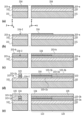
図1は、本開示の二重構造を含む光導波路部品の構成を示す図である。図1は、基板101の面(x-y面)に向かって2つの光導波路110、120を見た上面図、2本の光導波路の各コア104、103の中心を通る側面図(x-z面)、光導波路の長さ方向を垂直に切った断面の2つの端面図(y-z面)を含む。図1の光導波路部品100は、共通の基板101の上に形成された第1のコアサイズおよび対応するMFDを持つ第1の光導波路と、第2のコアサイズおよび対応するMFDを持つ第2の光導波路とが、光学的に接続された構造を備えている。第2の光導波路の第2のコアサイズは、第1の光導波路の第1のコアサイズよりも大きい。図1は2つの光導波路110、120が基板101上にモノリシック集積された光回路の一部だけを切り出して示しており、光導波路の数はこれに限られないし、また他の光導波路が光導波路部品100内に含まれていても良い。尚、図1の上面図(x-y面)では、最上部にあるクラッド105を取り除いて示している。
FIG. 1 is a diagram showing the configuration of an optical waveguide component including a double structure according to the present disclosure. FIG. 1 shows a top view of the two
2つの光導波路のより具体的な構成は、以下の通りである。第1の光導波路110では、コア104は第1の材料、クラッド103-1は第2の材料で形成し、第2の光導波路120では、コア103-2は第2の材料、クラッド105、102は第3の材料で形成する。本開示の光導波路部品100では、第1の材料、第2の材料および第3の材料の屈折率n1、n2、n3の関係が、第1の材料の屈折率n1が最も高く、第3の材料の屈折率n3が最も低いという関係を満たしていれば、各光導波路の材料の種類は問わない。要するに3つの材料の屈折率n1、n2、n3に、次式が成立していれば良い。
n1 > n2 > n3 式(1)A more specific configuration of the two optical waveguides is as follows. In the first
n 1 > n 2 > n 3 formula (1)
光導波路の長さ方向に垂直に切った断面(端面図)を見たとき、光学的に接続される2つの光導波路110、120は、第1の光導波路110のコア104が第2の光導波路のコア103に内包されていることがわかる。図1の上面図および側面図では、2つの光導波路の領域を区別して示すために、点線を用いて境界を示しているが、後述する作製プロセスを参照すれば明らかなように2つの光導波路の間に物理的な境界は存在しない。第2の材料について、第1の光導波路のクラッド103-1(103-1a、103-1b)および第2の光導波路のコア103-2(103-2a、103-2b)は2つの光導波路110、120を通して、一体とみなすことができる。光導波路の長さ方向に垂直な断面を見て、あたかも鉛筆とその芯のように、第2の光導波路のコア領域の内部に、第1の光導波路のコア領域が内包されている関係にある。さらに図1の光導波路部品100では、光導波路の長さ方向に垂直な断面で見たとき、第1の光導波路のコア領域は第2の光導波路のコア領域内に含まれ、2つのコアの中心高さが一致するように構成されている。このような光導波路の「二重構造」または「入れ子様構造」によって、図5に示した従来技術のモノリシック集積におけるコアの中心高さ位置のずれによる損失の問題を解消できる。
When looking at a cross section (end view) taken perpendicular to the length direction of the optical waveguide, the two
以下の実施形態の説明では具体例として、第1の材料がSi、第2の材料が相対的に屈折率の高いSiO2、第3の材料が相対的に屈折率の低いSiO2の場合で説明する。この材料例の場合、屈折率の大きさを、Si > 高屈折率SiO2 > 低屈折率SiO2の関係で表せる。2種類の光導波路の各部に使用できる材料はこれらだけに限られず、例えば第1の材料としてSi、SiN、SiONなどを使用することができる。また、第2の材料および第3の材料としてSiO2、SiOx、ポリマーなどを使用できる。以下、上述の具体的な材料を例に図1の光導波路部品の構造を説明する。In the following description of the embodiment, as a specific example, the first material is Si, the second material is SiO 2 with a relatively high refractive index, and the third material is SiO 2 with a relatively low refractive index. explain. In the case of this material example, the magnitude of the refractive index can be expressed by the relationship Si>high refractive index SiO2 >low refractive index SiO2 . The materials that can be used for each part of the two types of optical waveguides are not limited to these, and for example, Si, SiN, SiON, etc. can be used as the first material. Moreover, SiO 2 , SiOx, polymer, etc. can be used as the second material and the third material. Hereinafter, the structure of the optical waveguide component shown in FIG. 1 will be explained using the above-mentioned specific materials as an example.
再び図1に戻ると、光導波路部品100は基板101上に構成されている。基板101は、その直上にSiO2層を成膜可能な、表面が平滑な基板である。基板101の上には、屈折率の最も小さい第3の材料であるSiO2層102を備える。図1の上面図を参照すると、基板101の上に、第1の光導波路110および第2の光導波路120が構成されている。第1の光導波路110は、屈折率の最も大きいSiコア104を備え、上面図にあるようにSiコア104-2と、第2の光導波路120に向かって幅が狭まるテーパ導波路104-1とからなる。断面図を参照すれば、Siコア104は、下側のSiO2コア部103-1aの上に作製され、さらにSiコア104の上を覆うように上側のSiO2コア部103-1bが作製されている。Returning to FIG. 1 again, the
第2の光導波路120は、SiO2層102上のSiO2コア103を備え、側面図を参照すればSiO2コア103は上側のSiO2コア部103-2bと、下側のSiO2コア部103-2aの2つの部分から成る。以下の説明では、簡単のためSiO2コア103と記載する場合は、2つの光導波路に渡った4つのコア部103-1a、103-1b、103-2a、103-2bのSiO2領域の全体を指すものとする。SiO2コア103は、屈折率が中間の値を持つ第2の材料から構成されることになる。後述するように、上下のコア部103-2a、103-2bは別の工程により作製されるため、厳密に完全に同一の屈折率にするのが難しい場合もある。しかしながら、SiO2コア103は第2の光導波路120では、上下のコア部103-2a、103-2bが文字通り光導波路の「コア」として機能するよう、概ね同一の屈折率となるよう構成される。一方、第1の光導波路110では、上下のコア部103-1a、103-1bが実際には光導波路の「クラッド」として機能している点に留意されたい。The second
本開示の光導波路部品100では、高屈折率差導波路である第1の光導波路110の上層クラッド103-1b、下層クラッド103-1aにおける材料を、低屈折率差導波路である第2の光導波路120のコア103の材料と同一にしている点に注目すべきである。図4とともに後述する製造方法でも述べる通り、4つのコア部からなるSiO2コア103の内、下層のコア部103-1a、103-2aのSiO2領域(103-a)が1つの工程で作成される。また、4つのコア部からなるSiO2コア103の内、上層のコア部103-1b、103-2bのSiO2領域(103-b)も、1つの工程で作成される。本開示の光導波路部品100は、一般的な積層工程による光導波路部品の作製と同等の簡単なプロセスで、屈折率の異なるコアを有する2種類の光導波路を低損失に接続する構成を実現できる。図5の従来技術のSSC構造部で説明したような、SOI基板のBOX層を削り取るエッチング処理などは不要である。In the
2つの光導波路110、120の全体は、屈折率の最も小さい第3の材料によるSiO2層105の上側クラッドで覆われている。したがって、第1の光導波路110のSiコア104は、二重構造のクラッドによって囲まれている点にも留意されたい。The two
図1の光導波路部品の構成で屈折率の大きいものから順に並べれば、Siコア104 → SiO2コア103 → SiO2クラッド102、105の関係となる。すなわちSiO2コア部103-2a、103-2bの屈折率は、SiO2層102およびSiO2層105のクラッドの屈折率よりも大きい関係にある。ここでSiO2層102およびSiO2層105の屈折率は、同じである必要は無いことに留意されたい。すなわちSiO2層102、105の屈折率が、第2の光導波路のSiO2コア103-2よりも小さい限り、第2の光導波路120で光をコア内に閉じ込めて光導波路として機能できるからである。以下、図1の光導波路部品の各部およびコアの「二重構造」について、さらに詳細に説明する。
[第1の実施形態:光導波路の構成]
図1の光導波路部品100には、2種類の光導波路が存在している。すなわち1つは、SiO2コア部103-1aをアンダークラッド、Siコア104をコア、SiO2コア部103-1bをオーバークラッドとする第1の光導波路110である。もう1つは、SiO2層102をアンダークラッド、SiO2コア103をコア、SiO2層105をオーバークラッドとする第2の光導波路120である。If the configuration of the optical waveguide component in FIG. 1 is arranged in descending order of refractive index, the relationship will be
[First embodiment: Configuration of optical waveguide]
The
第1の光導波路110において、Siコア104は「クラッド」として機能するSiO2コア部103-1aとSiO2コア部103-1bの間に挟まれており、さらにSiコア104の幅はSiO2コア部103-1の幅よりも狭い構造となっている。したがって光導波路部品100は、平面光回路でありながら、第1の光導波路のSiコア104の断面領域が、第2の光導波路のSiO2コア103の断面領域内に完全に収まるようなコアの「二重構造」を持っている。また図1の左側の端面図から明らかなように、第1の光導波路110におけるSiコア104は、SiO2コア部103-1による内側クラッド、さらにSiO2層103、105による外側クラッドを備えた、クラッドの「二重構造」を持っているとも言える。In the first
したがって本発明は、基板101の上に、異なるモードフィールド径(MFD)を有する光導波路を形成した光導波路部品であって、第1の材料による第1のコア104、および、前記第1のコアの上下に形成された、第2の材料によるクラッド103-1a、103-1bを含む第1の光導波路110と、前記第1のコアに沿って、前記クラッドから延長して形成された前記第2の材料による第2のコア103、前記基板と前記第2のコアの間に構成された、第3の材料による下側クラッド102、および前記第2のコアの上に構成された上側クラッド105を含む第2の光導波路120とを備え、前記光導波路の長さ方向に垂直な断面において、前記第1のコア104の領域は、前記第2のコアの領域103に内包されており、前記第1の材料は最も屈折率が大きく、前記第3の材料は最も屈折が小さいことを特徴とする光導波路部品として実施できる。
Therefore, the present invention provides an optical waveguide component in which optical waveguides having different mode field diameters (MFD) are formed on a
光導波路部品100では、コア内を伝搬する光のMFDを徐々に拡大させるSSC領域130において、上述のコアの二重構造を備えている必要がある。すなわち、コア内を伝搬する光のMFDを徐々に拡大させるSSC領域130は、第1の光導波路内のコアの二重構造部分に形成することが望ましい。SSC機能のための構造は特定のものに限定されないが、図1のSSC領域130のように、Siコア104を一定幅のコア104-2から先細りのテーパ形状部104-1を経る構造によって実現できる。またSiコア104の高さが徐々に低くなる基板垂直方向(z軸方向)のテーパ形状を有しても良い。Siコア104が光の伝搬方向(x軸方向)に分断されたセグメント状の構造によって実現することもできる。すなわちSiコア104を、コアが形成されている領域(セグメント)と形成されていない領域が交互に繰り返されるようにセグメント化することで、光の閉じ込めを次第に弱くし、断熱遷移を生じさせる。さらに、テーパ形状およびセグメント形状の両方を組み合わせて、SSC領域を構成しても良い。
The
一方、第1の光導波路110においてSSC機能の無い、接続部の境界から離れた領域においては、必ずしも上述のコアの二重構造を備えている必要は無い。光導波路部品100で、第1の光導波路110および第2の光導波路120の接続部付近から遠ざかった図1に示さない領域では、図1の第1の光導波路110および第2の光導波路120は、それぞれの構造から別の構造へ遷移をしていっても良い。
On the other hand, in the region of the first
図2は、二重構造および別の導波路構造を含む光導波路部品の構成を示す図である。図2の(a)、(b)は、それぞれ図1の光導波路部品の変形例の構成を示し、基板面(x-y面)を見た上面図、光導波路を含む基板面に垂直な断面(x-z面)を見た側面図、光導波路の長さ方向に垂直な断面(y-z面)を見た端面図を含む。また各上面図は、最上部にあるクラッド105を取り除いて示している。
FIG. 2 is a diagram showing the configuration of an optical waveguide component including a double structure and another waveguide structure. 2(a) and 2(b) respectively show the configuration of a modified example of the optical waveguide component in FIG. It includes a side view as seen in a cross section (xz plane) and an end view as seen in a cross section (yz plane) perpendicular to the length direction of the optical waveguide. Moreover, each top view is shown with the
図2の(a)の光導波路部品100-1は、第1の光導波路110のオーバークラッドとして機能するコア部103-1bを、SSC領域130内のテーパ形状部104-1の上だけに限定して備えている。すなわち、第1の光導波路110の矩形のSiコア104-2の上は、オーバークラッドとして機能するSiO2層105で直接覆われている。図2の(a)の構造の場合、SSC領域130の外におけるSiコア104では、第2の材料のSiO2コア部103-1aのアンダークラッドおよび第3の材料のSiO2層105のオーバークラッドによって光が閉じ込められる。光導波路としての機能は、図1の第1の光導波路110の場合と何ら変わりがない。図2(a)の光導波路部品100-1のSiコア104の先では、シリコン細線導波路の光回路が構成されることになるため、第2の材料のコア103のためのパターンニングが無くなり、Siコア104の先では、シリコン細線導波路の光回路が構成されることになる。その光回路部においては、シリコン細線導波路コアの上で、平面光導波路コアの材料層を形成したりパターニングしたりする必要がないため、シリコン回路を劣化させる要因が減る。In the optical waveguide component 100-1 in FIG. 2(a), the core portion 103-1b, which functions as an overclad of the first
図2の(b)の光導波路部品100-2は、第1の光導波路110のオーバークラッドとして機能するコア部103-1bをSSC領域130内のテーパ形状部104-1の上だけに限定して備えている。図2の(b)の構成では、第1の光導波路110の矩形のSiコア104-2の上にはオーバークラッドが無く、Siコア104がむき出しになった構成である。この構造でも、SSC領域130外のSiコア104では、第2の材料のSiO2コア部103-1aによるアンダークラッドおよびSiコアとの屈折率差の大きい空気によって光が閉じ込められる。図2(b)の光導波路部品100-2のSiコア104の先にあるシリコン細線導波路において、より強く光を閉じ込め、コアをより細くし、曲げ半径をより小さくできるメリットがある。In the optical waveguide component 100-2 in FIG. 2B, the core portion 103-1b, which functions as an overclad of the first
上述のように、図1の第1の光導波路110の先において、図2の(a)、(b)の様に光導波路の形態を変えることもできるし、第2の光導波路120の先において光導波路の形態を変えることもできる。本開示の光導波路部品におけるコアサイズの異なる2つの光導波路のコアの二重構造は、SSC領域130において必要なものであって、図1の光導波路部品100は集積化した光回路の一部であることに留意されたい。
[各層の厚み、中心高さ合わせ構造]
ここで再び図1の光導波路部品100に戻ると、アンダークラッドのSiO2層102およびオーバークラッドのSiO2層105の厚さは、第2の光導波路120のSiO2コア103内を伝搬する光のモードフィールドが十分収まるものであれば良い。すなわちクラッド層102、105は、第2の光導波路120を伝搬する光のモードフィールドが、基板101やオーバークラッドSiO2層105直上の空気層にまで染み出さない程度の厚さであれば良い。一般的には、クラッドSiO2層102、105の厚さは数10μm程度であれば十分である。As mentioned above, the shape of the optical waveguide can be changed at the end of the first
[Thickness of each layer, center height alignment structure]
Returning again to the optical waveguide component 100 in FIG. It is sufficient as long as the mode field of . That is, the cladding layers 102 and 105 need only have a thickness that does not allow the mode field of light propagating through the second
基板に垂直な方向において、第1の光導波路110のSiコア104の中心高さと、第2の光導波路120のSiO2コア103の中心高さは、次の様に設定することで一致させることができる。すなわち、下側のSiO2層103-1a、103-2aの厚さを、SiO2コア103の全体の高さの1/2およびSiコア104の高さの1/2の間の差に設定すれば良い。このとき2つの光導波路のコア同士の中心高さを完全に一致させることが可能で、従来技術のSSC構造部における断熱結合の不完全さや、突合せ結合効率の悪化による接続性の問題を解消する。
[モード数の非限定、コアサイズ、シングルモードの場合のMFD]
図1の光導波路部品100において、第1の光導波路110および第2の光導波路120のいずれも、コア断面サイズに上限はなく、使用する光信号の波長に対して、複数のモードの光を伝搬させるマルチモードの光導波路とすることもできる。また、コア断面サイズを小さくすることで、最低次のモードのみを伝搬させるシングルモードの光導波路とすることもできる。In the direction perpendicular to the substrate, the center height of the
[MFD with unlimited number of modes, core size, and single mode]
In the
第1の光導波路110はSi層をコア104とし、図1のようにSiO2層103-1a、103-1bを、または図2の(b)のように空気をクラッドとし、コア-クラッド間の屈折率差が大きい。このため、コア断面サイズを数百nmまで小さくすることができる。一方、コアおよびクラッドの材料としてSiO2層を用いる第2の光導波路120は、第1の光導波路110に比べてコア-クラッド間の屈折率差が小さい。このため、第2の光導波路120のコア断面サイズは、数μm~10μm角程度までとなる。The first
第1の光導波路110、第2の光導波路120のいずれもシングルモードの光導波路である場合、コア断面サイズは第1の光導波路で数百nm程度、第2の光導波路120で数μm~10μm程度となる。このため、2つの光導波路のコア内を伝搬する光のMFDは著しく異なり、第2の光導波路120のMFDが第1の光導波路110のMFDに比べて大きな値となる。
[結合方式]
シングルモードとなる光導波路のコア同士を接続させる方式は、2種類に大別される。1つの接続方式は断熱結合であり、伝搬方向に対して、2つの光導波路の両コアが接するように配置し、一方の光導波路コアを、先細りのテーパ形状にするなどしてコア内を伝搬するモードの等価屈折率を徐々に減少させる。このような構成により、もはや閉じ込めきれなくなったモードの光エネルギーが、隣接する他方の光導波路コアへと断熱的に遷移する。もう1つの接続方式は突合せ結合であり、コアどうしの端面を突き合わせて配置し、2つの光導波路の両コアに存在するモードプロファイルの重なり積分でその結合効率が規定される。When both the first
[Join method]
Methods for connecting the cores of single-mode optical waveguides are roughly divided into two types. One connection method is adiabatic coupling, in which both cores of two optical waveguides are placed in contact with each other in the propagation direction, and one optical waveguide core is made into a tapered shape to prevent propagation within the core. Gradually decrease the equivalent refractive index of the mode. With this configuration, the optical energy of the mode that can no longer be confined is adiabatically transferred to the other adjacent optical waveguide core. Another connection method is butt coupling, in which the cores are arranged with their end surfaces butted against each other, and the coupling efficiency is defined by the overlapping integral of the mode profiles existing in both cores of the two optical waveguides.
本開示の光導波路部品100で、第1の光導波路110および第2の光導波路120のいずれもシングルモード光導波路である場合、2種類の光導波路を接続するSSC領域130において、断熱結合および突合せ結合の一方または両方の接続方式を利用する。
In the
第2の光導波路120は、第1の光導波路110に比べて大きなMFDを示す。第1の光導波路110および第2の光導波路120を低損失に接続するためには、2種類の光導波路の境界近傍でMFDを整合させることが望ましい。MFDの整合を実現するため、第1の光導波路110のMFDを、第2の光導波路120のMFDへ合わせるように徐々に拡大させる。このMFD拡大機能を実現する構造は問わないが、例えば、図1のSSC領域130のようにSiコアを先細りのテーパ形状104-1とする構造がある。Siコア104のMFDを徐々に拡大させるには、Siコア104内のモードの等価屈折率を徐々に減少させれば良い。SSC領域130のSiコアを、先細りのテーパ形状部分104-1とすることで、第2の光導波路120に近づくにつれ等価屈折率を減少させることができる。Siコア104-1が上下のSiO2コア部103-1a、103-1bに挟まれている領域において、テーパ形状のSiコアにより等価屈折率を減少させることで、Siコア内の光エネルギーの一部またはすべてを、第2の光導波路120のSiO2コア103へと断熱的に遷移させられる。The second
Siコア104内の光エネルギーの一部は、SiO2コア103との断熱結合をしないでSiコア104内を伝搬し、第1の光導波路と第2の光導波路の境界にまで到達することがある。このような場合、第1の光導波路110のSiコア104は境界において第2の光導波路120のSiO2コア103と突合せ結合される。Siコア104内で断熱結合をしなかった光エネルギーの一部分は、Siコア104とSiO2コア103の中心高さが一致するように光導波路部品100を作製することで効率的に結合できる。2つのコアの中心高さを一致させることにより、モードフィールドの重なり積分で規定される突合せ結合効率を高く保ち、2つの光導波路間で低損失に光エネルギーを結合させることができる。A part of the optical energy within the
以上詳細に述べたように、実施形態の光導波路部品100によれば、異なる材料の光導波路を共通の単一の基板上にモノリシック集積可能であり、モードフィールドの大きさが異なる2種類の光導波路を低損失に接続する構成を提供できる。上述の図1の実施形態では、2つの光導波路を低損失に結合して、連続した単一の光導波路を構成していたが、異なる材料の複数の光導波路同士を低損失に結合させることもできる。
[第2の実施形態:ピッチ変換]
図3は、第2の実施形態の光導波路部品の構成を示す図である。第2の実施形態の光導波路部品300では、複数の第1の光導波路と、同数の第2の光導波路とを低損失に結合する。複数の第1の光導波路の内の1つの第1の光導波路と、対応する第2の光導波路との間の構造は、図1に示した第1の実施形態の光導波路部品100と同様であり、説明を省略する。As described in detail above, according to the
[Second embodiment: Pitch conversion]
FIG. 3 is a diagram showing the configuration of an optical waveguide component according to the second embodiment. In the
第1の実施形態で説明した通り、第1の光導波路のSiコア104では、第2の光導波路と比較して極小断面内に光を閉じ込め可能である。したがって狭い領域に複数のSiコア104のための多くのコアパターンを作成したい場合、コア間ピッチを数μm程度にまで狭めることができる。一方、第1の光導波路より大きいコアサイズを持つ第2の光導波路は、できるだけコア幅を細くした場合でも、少なくとも数μm~10μm角程度のコア断面サイズが必要である。このため、複数の第2の光導波路のSiO2コア103を配列する場合に想定されるコア間ピッチは、数10μm~数100μmとなる。As described in the first embodiment, the
図3の光導波路部品300において、複数の第1の光導波路と同数の対応する第2の光導波路の接続を高密度で行う場合、複数のSiコア104と複数のSiO2コア103を、同一のコア間ピッチにて形成する必要がある。その際のコア間ピッチは任意であるが、高密度に配線する場合、第2の光導波路の最小コア間ピッチに合わせて、たとえば数10μmとすることが望ましい。In the
一方、第1の光導波路との接続部から離れた、例えば基板上の第2の光導波路の別の端面107では、接続部とは異なるコア間ピッチとする場合がある。光ファイバアレイに接続する場合であれば、光ファイバのコア間ピッチの規格である125μmや250μmに合わせ、第2の光導波路の端面107付近でのSiO2コア103のコア間ピッチが決定される。このような場合、第1の光導波路との接続部付近から、接続部から離れた別の端面107まで、第2の光導波路のSiO2コア103に対して、導波路間間隔を拡張する。導波路間間隔を拡張する領域108は、直線、曲線、または、直線および曲線の組み合わせを含むパターニングにより構成される。この導波路間間隔を拡張する領域108により、複数の第1の光導波路から第2の光導波路の基板の別の端面107まで、第2の光導波路は滑らかに延長され、光ファイバアレイ106まで光学的に接続することができる。On the other hand, for example, another
以上、本実施形態によれば、MFDが大きく異なる2種類の光導波路について、複数の光導波路の接続部が配列される場合にも、本開示の接続部の構成で両導波路を低損失に接続する光導波路部品を提供できる。
[第3の実施形態:製造方法]
図4は、本開示の光導波路部品の製造方法のプロセスを説明する図である。本実施形態は、第1の実施形態および第2の実施形態で示した光導波路部品の製造方法であり、作製される光導波路部品の構造については、第1の実施形態および第2の実施形態に記載の通りであるため、説明を省略する。図4の(a)~(e)は、図1の光導波路部品100が作製されるまでステップを順に示している。As described above, according to the present embodiment, even when connecting portions of a plurality of optical waveguides are arranged for two types of optical waveguides with significantly different MFDs, the configuration of the connecting portion of the present disclosure allows both waveguides to have low loss. We can provide optical waveguide components for connection.
[Third embodiment: manufacturing method]
FIG. 4 is a diagram illustrating the process of the method for manufacturing an optical waveguide component of the present disclosure. This embodiment is a method for manufacturing the optical waveguide component shown in the first embodiment and the second embodiment, and the structure of the optical waveguide component to be manufactured is the same as that in the first embodiment and the second embodiment. Since it is as described in , the explanation will be omitted. 4(a) to 4(e) sequentially show the steps until the
図4の(a)を参照すると、その上にSiO2層を成膜可能な程度に表面が平滑な基板101の上に、SiO2層102(第1の層)を形成する。基板101の具体例として、ガラス基板等が挙げられるが、特にSi基板が好適である。SiO2層102の形成方法については、形成した層の直上にさらに他の層を形成可能な程に、均一かつ平滑な層を形成できればその方法は問わない。一例を挙げれば、火炎堆積法などのSiO2層の成膜方法がある。SiO2層102の直上には、SiO2層102よりも高い屈折率を有するSiO2層203-a(第2の層)を形成する。SiO2層203-aの形成にあたっては、GeO2、ZrO2、HfO2、P2O5やB2O3などを添加することでその屈折率を制御しても良い。SiO2層203-aをCMP(Chemical Mechanical Polishing)などの手段により平坦化する工程を経たのち、SiO2層203-aの直上にSi層204(第3の層)を形成し、平坦化する。Referring to FIG. 4A, a SiO 2 layer 102 (first layer) is formed on a
ここで図1を再び参照すれば、上述のSiO2層203-aが、図1の2つの光導波路に渡った4つのコア部103-1a、103-1b、103-2a、103-2bのSiO2領域の内の、下側の103-1a、103-2aのための層となる。Referring again to FIG. 1, the above-mentioned SiO 2 layer 203-a forms the four core portions 103-1a, 103-1b, 103-2a, and 103-2b across the two optical waveguides in FIG. This becomes a layer for the lower portions 103-1a and 103-2a in the SiO 2 region.
Si層204の形成にあたっては、アモルファスシリコンのスパッタリングなどで製膜をしても良いし、別のSi基板を基板101の上面(SiO2層203-a上)に貼り合わせた後に、所望のSi膜厚を得ても良い。(a)の状態は、一般的なSOI基板において、表層のSi層の下に単層のSiO2層すなわちBOX(Buried OXide)層を形成する代わりに、屈折率の異なる2層のSiO2層、すなわちSiO2層102およびSiO2層203-aが形成されたものと言える。In forming the
次に図4の(b)を参照すると、Si層204を、光導波路コアとして光を伝搬させることができるように加工して、第1の光導波路のSiコア104を作製する。図4の(b)には示されていないが、Siコア104の形成と併せて、Siコア104の先のSiフォトニクスの光回路を形成しても良い。
Next, referring to FIG. 4B, the
さらに図4の(c)を参照すると、SiO2層203-aおよびSiコア104の直上に、SiO2層203-b(第4の層)を形成する。このSiO2層203-bは、SiO2層203-aと同程度の屈折率を有する。図1を再び参照すれば、上述のSiO2層203-bが、図1の2つの光導波路に渡った4つのコア部103-1a、103-1b、103-2a、103-2bのSiO2領域の内、上側の103-1b、103-2bのための層となる。Further referring to FIG. 4C, a SiO 2 layer 203-b (fourth layer) is formed directly above the SiO 2 layer 203-a and the
次に図4の(d)を参照すると、SiO2層203-aとSiO2層203-bを一括して加工して、第2の光導波路のコアとして光を伝搬させることができるSiO2コア103(コア部103-2a、103-2b)を得る。同時に第1の光導波路の「クラッド」としてコア部103-1a、103-1bも形成される。この段階で、すでに加工されているSiコア104の幅に比べて、一括加工されるSiO2コア103の幅が広いことが望ましい。これは、SiO2コア103の加工時に、既に加工されているSiコア104の側壁に影響を与えないためである。Next, referring to FIG. 4(d), the SiO 2 layer 203-a and the SiO 2 layer 203-b are collectively processed to form an SiO 2 layer that can be used as the core of the second optical waveguide to propagate light. Core 103 (core parts 103-2a, 103-2b) is obtained. At the same time, core portions 103-1a and 103-1b are also formed as the "cladding" of the first optical waveguide. At this stage, it is desirable that the width of the SiO 2 core 103 that is processed all at once is wider than the width of the
最後に図4の(e)を参照すると、SiO2コア103よりも低い屈折率を有するSiO2層105(第5の層)を形成することで、光導波路部品100を作製することができる。Finally, referring to FIG. 4(e), the
上述のように本発明は、異なるモードフィールド径(MFD)を有する第1の光導波路110および第2の光導波路120を含む光導波路部品100の製造方法であって、基板101上に、下側クラッドとなる第1の層102を形成するステップと、前記第1の層よりも高い屈折率を有する材料により、前記第2の光導波路の下側コアのための第2の層203-aを形成するステップと、前記第2の層よりもさらに高い屈折率を有する材料により、前記第1の光導波路のコアのための第3の層204を形成するステップと、前記第3の層を加工して、前記第1の光導波路のコア104を形成するステップと、前記第2の層と同程度の屈折率を有する材料により、前記第2の光導波路の上側コアのための第4の層203-bを形成するステップと、前記第2の層および前記第4の層を一括して加工して、前記第2の光導波路のコア103を形成するステップと、前記第2の層および前記第4の層よりも低い屈折率を有する材料により、上側クラッドとなる第5の層103を形成するステップとを備える光導波路部品の製造方法として実施できる。
As described above, the present invention provides a method for manufacturing an
上述のように、本実施形態によれば、第1の実施形態および第2の実施形態に示した光導波路部品の簡単な製造方法を提供することができる。 As described above, according to this embodiment, it is possible to provide a simple method for manufacturing the optical waveguide component shown in the first embodiment and the second embodiment.
以上詳細に説明したように、第1、第2の実施形態の光導波路部品および第3の実施形態の光導波路部品の製造方法によれば、一般的な積層工程による光導波路部品作製プロセスと同等の簡単なプロセスで、屈折率の異なるコアを有する2種類の光導波路を低損失に接続できる。特に、2つの光導波路のコア中心高さが互いに一致するような構造とすることで、より低損失に接続することができる。本発明により、MFDの大きく異なる光導波路同士を簡易に接続できる光導波路部品を提供することができる。 As explained in detail above, the method for manufacturing the optical waveguide components of the first and second embodiments and the optical waveguide component of the third embodiment is equivalent to the optical waveguide component manufacturing process using a general lamination process. With this simple process, two types of optical waveguides having cores with different refractive indexes can be connected with low loss. In particular, by configuring the two optical waveguides so that their core center heights match each other, it is possible to connect the two optical waveguides with lower loss. According to the present invention, it is possible to provide an optical waveguide component that can easily connect optical waveguides with significantly different MFDs.
本発明は、光通信を用いる装置に利用できる。 INDUSTRIAL APPLICATION This invention can be utilized for the apparatus which uses optical communication.
Claims (5)
複数の第1の光導波路と、
前記第1の光導波路とは異なるモードフィールド径(MFD)を持ち、前記第1の光導波路と光学的に結合した、対応する複数の第2の光導波路とを有する光導波路部品であって、
前記複数の第2の光導波路は、前記複数の第1の光導波路とは異なる間隔で配置されており、前記複数の第1の光導波路と前記複数の第2の光導波路の間に、導波路間間隔を拡張する領域を有し、
前記複数の第1の光導波路の各々は、
第1の材料による第1のコア、および、前記第1のコアの上下に形成された、第2の材料によるクラッドを含み、
前記複数の第2の光導波路の各々は、
前記第1のコアに沿って、前記クラッドから延長して形成された前記第2の材料による第2のコア、前記基板と前記第2のコアの間に形成された、第3の材料による下側クラッド、および、前記第2のコアの上に形成された上側クラッドを含み、
前記光導波路の長さ方向に垂直な断面において、前記第1のコアの領域は、前記第2のコアの領域に内包されており、
前記第1の材料は最も屈折率が大きく、前記第3の材料は最も屈折率が小さく、
前記第1のコアの先端部は、前記第1のコアが断続的に形成されたセグメント構造を有し、前記第1の光導波路を伝搬する光信号のMFDを変化させるスポットサイズ変換領域を構成しており、
前記第1の光導波路の前記第1のコアから延長して形成された第3のコア、および、前記第1の光導波路の前記第1のコアの下に形成された前記クラッドから延長して形成された下側クラッドのみを含む、前記スポットサイズ変換領域の外に形成された第3の光導波路をさらに備えた
ことを特徴とする光導波路部品。 on the board,
a plurality of first optical waveguides;
An optical waveguide component having a plurality of corresponding second optical waveguides having a mode field diameter (MFD) different from that of the first optical waveguide and optically coupled to the first optical waveguide,
The plurality of second optical waveguides are arranged at different intervals from the plurality of first optical waveguides, and there is a guide between the plurality of first optical waveguides and the plurality of second optical waveguides. It has a region that expands the inter-wavelength spacing,
Each of the plurality of first optical waveguides is
A first core made of a first material , and a cladding made of a second material formed above and below the first core ,
Each of the plurality of second optical waveguides is
a second core made of the second material extending from the cladding along the first core; a bottom made of a third material formed between the substrate and the second core; a side cladding and an upper cladding formed on the second core ;
In a cross section perpendicular to the length direction of the optical waveguide, the first core region is included in the second core region,
the first material has the highest refractive index, the third material has the lowest refractive index,
The tip of the first core has a segment structure in which the first core is intermittently formed, and constitutes a spot size conversion region that changes the MFD of the optical signal propagating in the first optical waveguide. and
a third core formed extending from the first core of the first optical waveguide; and a third core extending from the cladding formed below the first core of the first optical waveguide. further comprising a third optical waveguide formed outside the spot size conversion region, including only the formed lower cladding.
An optical waveguide component characterized by:
前記第3のコアの上が、前記第2の光導波路の前記上側クラッドから延長して形成された上側クラッドでさらに覆われていることを特徴とする請求項1に記載の光導波路部品。2. The optical waveguide component according to claim 1, wherein the third core is further covered with an upper cladding extending from the upper cladding of the second optical waveguide.
前記第1のコアの中心高さおよび前記第2のコアの中心高さが一致することを特徴とする請求項1または2に記載の光導波路部品。 The thickness of the cladding formed under the first core is set to a difference between 1/2 of the height of the second core and 1/2 of the height of the first core. and
The optical waveguide component according to claim 1 or 2, wherein the center height of the first core and the center height of the second core are the same.
前記母材の違いによって屈折率の違いが生じたもの、または、
前記母材への不純物の添加量の違いによって屈折率の違いが生じたもののいずれかであること特徴とする請求項1乃至4いずれかに記載の光導波路部品。 The first material, the second material, and the third material have a base material of Si, SiN, SiON, SiO x , or a polymer,
The refractive index differs due to the difference in the base material, or
5. The optical waveguide component according to claim 1, wherein the optical waveguide component has a difference in refractive index due to a difference in the amount of impurity added to the base material.
Applications Claiming Priority (1)
| Application Number | Priority Date | Filing Date | Title |
|---|---|---|---|
| PCT/JP2020/031934 WO2022044101A1 (en) | 2020-08-25 | 2020-08-25 | Optical waveguide component and method for manufacturing same |
Publications (2)
| Publication Number | Publication Date |
|---|---|
| JPWO2022044101A1 JPWO2022044101A1 (en) | 2022-03-03 |
| JP7401823B2 true JP7401823B2 (en) | 2023-12-20 |
Family
ID=80352802
Family Applications (1)
| Application Number | Title | Priority Date | Filing Date |
|---|---|---|---|
| JP2022544918A Active JP7401823B2 (en) | 2020-08-25 | 2020-08-25 | Optical waveguide components and their manufacturing method |
Country Status (3)
| Country | Link |
|---|---|
| US (1) | US20230280524A1 (en) |
| JP (1) | JP7401823B2 (en) |
| WO (1) | WO2022044101A1 (en) |
Citations (6)
| Publication number | Priority date | Publication date | Assignee | Title |
|---|---|---|---|---|
| JP2004258610A (en) | 2003-02-04 | 2004-09-16 | Tdk Corp | Spot-size converter element, its manufacture method and waveguide-embedding optical circuit using spot-size converter element |
| JP2005538426A (en) | 2002-08-20 | 2005-12-15 | エルエヌエル・テクノロジーズ・インコーポレイテッド | Embedded mode converter |
| US20090297093A1 (en) | 2008-05-28 | 2009-12-03 | Lightwire, Inc. | Low index, large mode field diameter optical coupler |
| WO2012114866A1 (en) | 2011-02-21 | 2012-08-30 | 日本電気株式会社 | Spot size converter and manufacturing method thereof |
| JP2016018191A (en) | 2014-07-11 | 2016-02-01 | 沖電気工業株式会社 | Spot size converter and manufacturing method thereof |
| US20190310423A1 (en) | 2018-04-04 | 2019-10-10 | Finisar Corporation | Adiabatically coupled photonic systems with fan-out interposer |
Family Cites Families (1)
| Publication number | Priority date | Publication date | Assignee | Title |
|---|---|---|---|---|
| JPH05249331A (en) * | 1992-01-09 | 1993-09-28 | Nippon Telegr & Teleph Corp <Ntt> | Waveguide type beam spot conversion element and production thereof |
-
2020
- 2020-08-25 JP JP2022544918A patent/JP7401823B2/en active Active
- 2020-08-25 US US18/005,711 patent/US20230280524A1/en active Pending
- 2020-08-25 WO PCT/JP2020/031934 patent/WO2022044101A1/en active Application Filing
Patent Citations (6)
| Publication number | Priority date | Publication date | Assignee | Title |
|---|---|---|---|---|
| JP2005538426A (en) | 2002-08-20 | 2005-12-15 | エルエヌエル・テクノロジーズ・インコーポレイテッド | Embedded mode converter |
| JP2004258610A (en) | 2003-02-04 | 2004-09-16 | Tdk Corp | Spot-size converter element, its manufacture method and waveguide-embedding optical circuit using spot-size converter element |
| US20090297093A1 (en) | 2008-05-28 | 2009-12-03 | Lightwire, Inc. | Low index, large mode field diameter optical coupler |
| WO2012114866A1 (en) | 2011-02-21 | 2012-08-30 | 日本電気株式会社 | Spot size converter and manufacturing method thereof |
| JP2016018191A (en) | 2014-07-11 | 2016-02-01 | 沖電気工業株式会社 | Spot size converter and manufacturing method thereof |
| US20190310423A1 (en) | 2018-04-04 | 2019-10-10 | Finisar Corporation | Adiabatically coupled photonic systems with fan-out interposer |
Also Published As
| Publication number | Publication date |
|---|---|
| JPWO2022044101A1 (en) | 2022-03-03 |
| US20230280524A1 (en) | 2023-09-07 |
| WO2022044101A1 (en) | 2022-03-03 |
Similar Documents
| Publication | Publication Date | Title |
|---|---|---|
| KR101121459B1 (en) | Method and apparatus for compactly coupling an optical fiber and a planar optical wave guide | |
| US9128240B2 (en) | Spot-size converter, manufacturing method thereof, and integrated optical circuit device | |
| WO2018113627A1 (en) | Optical edge coupler with controllable mode field for photonic chip | |
| US20190265415A1 (en) | Optical apparatus and methods of manufacture thereof | |
| US8000565B2 (en) | Buried dual taper waveguide for passive alignment and photonic integration | |
| JP6290742B2 (en) | Optical circuit component, and connection structure between optical circuit component and optical fiber | |
| US20060115215A1 (en) | Dual "cheese wedge" silicon taper waveguide | |
| CA2734614A1 (en) | Optical mode transformer, in particular for coupling an optical fiber and a high-index contrast waveguide | |
| JP2002122750A (en) | Structure for connecting optical waveguide | |
| CN210666088U (en) | Silicon optical mode spot mode converter | |
| JPH07110415A (en) | Optical waveguide, connecting device for optical waveguide and optical fiber | |
| CN114895402B (en) | Offset heat insulation guided wave system | |
| CN112470047B (en) | Silicon dioxide to silicon nitride PLC wave mode converter for hybrid device | |
| JP5438080B2 (en) | Spot size converter | |
| JP2004157530A (en) | Optical module | |
| JP7401823B2 (en) | Optical waveguide components and their manufacturing method | |
| WO2021178727A1 (en) | Evanescent coupler mode converters | |
| WO2022254701A1 (en) | Optical waveguide circuit and method for manufacturing same | |
| WO2024034131A1 (en) | Optical waveguide circuit and method for manufacturing optical waveguide circuit | |
| WO2023243014A1 (en) | Optical waveguide connection structure | |
| WO2023171581A1 (en) | Optical waveguide and method for manufacturing optical waveguide | |
| WO2023234111A1 (en) | Optical element and method for producing optical element | |
| JP7401824B2 (en) | Optical waveguide components and their manufacturing method | |
| RU2712985C1 (en) | Mode converter device | |
| WO2023223432A1 (en) | Mode field conversion optical circuit |
Legal Events
| Date | Code | Title | Description |
|---|---|---|---|
| A621 | Written request for application examination |
Free format text: JAPANESE INTERMEDIATE CODE: A621 Effective date: 20221125 |
|
| A131 | Notification of reasons for refusal |
Free format text: JAPANESE INTERMEDIATE CODE: A131 Effective date: 20230704 |
|
| A521 | Request for written amendment filed |
Free format text: JAPANESE INTERMEDIATE CODE: A523 Effective date: 20230815 |
|
| TRDD | Decision of grant or rejection written | ||
| A01 | Written decision to grant a patent or to grant a registration (utility model) |
Free format text: JAPANESE INTERMEDIATE CODE: A01 Effective date: 20231107 |
|
| A61 | First payment of annual fees (during grant procedure) |
Free format text: JAPANESE INTERMEDIATE CODE: A61 Effective date: 20231120 |
|
| R150 | Certificate of patent or registration of utility model |
Ref document number: 7401823 Country of ref document: JP Free format text: JAPANESE INTERMEDIATE CODE: R150 |