JP7381090B2 - Technique for measuring the non-uniformity of refractive index between plates of a light-guiding optical element (LOE) - Google Patents
Technique for measuring the non-uniformity of refractive index between plates of a light-guiding optical element (LOE) Download PDFInfo
- Publication number
- JP7381090B2 JP7381090B2 JP2020570496A JP2020570496A JP7381090B2 JP 7381090 B2 JP7381090 B2 JP 7381090B2 JP 2020570496 A JP2020570496 A JP 2020570496A JP 2020570496 A JP2020570496 A JP 2020570496A JP 7381090 B2 JP7381090 B2 JP 7381090B2
- Authority
- JP
- Japan
- Prior art keywords
- plates
- light
- reflected
- deviation
- interferogram
- Prior art date
- Legal status (The legal status is an assumption and is not a legal conclusion. Google has not performed a legal analysis and makes no representation as to the accuracy of the status listed.)
- Active
Links
- 238000000034 method Methods 0.000 title claims description 58
- 230000003287 optical effect Effects 0.000 title claims description 30
- 238000012545 processing Methods 0.000 claims description 21
- 238000003491 array Methods 0.000 claims description 7
- 238000004422 calculation algorithm Methods 0.000 claims description 5
- 238000000605 extraction Methods 0.000 claims description 5
- 238000013213 extrapolation Methods 0.000 claims description 4
- 238000001429 visible spectrum Methods 0.000 claims description 3
- 238000012360 testing method Methods 0.000 description 32
- 239000000758 substrate Substances 0.000 description 17
- 238000003860 storage Methods 0.000 description 7
- 238000004364 calculation method Methods 0.000 description 5
- 238000004519 manufacturing process Methods 0.000 description 5
- 238000000576 coating method Methods 0.000 description 4
- 238000010586 diagram Methods 0.000 description 4
- 239000004973 liquid crystal related substance Substances 0.000 description 4
- 238000005259 measurement Methods 0.000 description 4
- 238000000691 measurement method Methods 0.000 description 4
- 230000015654 memory Effects 0.000 description 4
- 230000006399 behavior Effects 0.000 description 3
- 239000011248 coating agent Substances 0.000 description 3
- 238000005516 engineering process Methods 0.000 description 3
- 210000000887 face Anatomy 0.000 description 3
- 230000006870 function Effects 0.000 description 3
- XUIMIQQOPSSXEZ-UHFFFAOYSA-N Silicon Chemical compound [Si] XUIMIQQOPSSXEZ-UHFFFAOYSA-N 0.000 description 2
- 230000005540 biological transmission Effects 0.000 description 2
- 238000004891 communication Methods 0.000 description 2
- 238000004590 computer program Methods 0.000 description 2
- 230000002950 deficient Effects 0.000 description 2
- 230000006866 deterioration Effects 0.000 description 2
- 238000011161 development Methods 0.000 description 2
- 230000001902 propagating effect Effects 0.000 description 2
- 210000001747 pupil Anatomy 0.000 description 2
- 229910052710 silicon Inorganic materials 0.000 description 2
- 239000010703 silicon Substances 0.000 description 2
- 108010076504 Protein Sorting Signals Proteins 0.000 description 1
- 238000004458 analytical method Methods 0.000 description 1
- 230000000712 assembly Effects 0.000 description 1
- 238000000429 assembly Methods 0.000 description 1
- 230000000052 comparative effect Effects 0.000 description 1
- 238000005520 cutting process Methods 0.000 description 1
- 230000001419 dependent effect Effects 0.000 description 1
- 238000013461 design Methods 0.000 description 1
- 230000001066 destructive effect Effects 0.000 description 1
- 238000011156 evaluation Methods 0.000 description 1
- 239000011521 glass Substances 0.000 description 1
- 230000005484 gravity Effects 0.000 description 1
- 238000000227 grinding Methods 0.000 description 1
- 210000003128 head Anatomy 0.000 description 1
- 229910052734 helium Inorganic materials 0.000 description 1
- 239000001307 helium Substances 0.000 description 1
- SWQJXJOGLNCZEY-UHFFFAOYSA-N helium atom Chemical compound [He] SWQJXJOGLNCZEY-UHFFFAOYSA-N 0.000 description 1
- 230000002452 interceptive effect Effects 0.000 description 1
- 239000000463 material Substances 0.000 description 1
- 230000001404 mediated effect Effects 0.000 description 1
- 229910052754 neon Inorganic materials 0.000 description 1
- GKAOGPIIYCISHV-UHFFFAOYSA-N neon atom Chemical compound [Ne] GKAOGPIIYCISHV-UHFFFAOYSA-N 0.000 description 1
- 230000010287 polarization Effects 0.000 description 1
- 238000005498 polishing Methods 0.000 description 1
- 238000000926 separation method Methods 0.000 description 1
- 238000010008 shearing Methods 0.000 description 1
- 230000009466 transformation Effects 0.000 description 1
Images


Classifications
-
- G—PHYSICS
- G01—MEASURING; TESTING
- G01N—INVESTIGATING OR ANALYSING MATERIALS BY DETERMINING THEIR CHEMICAL OR PHYSICAL PROPERTIES
- G01N21/00—Investigating or analysing materials by the use of optical means, i.e. using sub-millimetre waves, infrared, visible or ultraviolet light
- G01N21/17—Systems in which incident light is modified in accordance with the properties of the material investigated
- G01N21/41—Refractivity; Phase-affecting properties, e.g. optical path length
- G01N21/45—Refractivity; Phase-affecting properties, e.g. optical path length using interferometric methods; using Schlieren methods
-
- G—PHYSICS
- G01—MEASURING; TESTING
- G01M—TESTING STATIC OR DYNAMIC BALANCE OF MACHINES OR STRUCTURES; TESTING OF STRUCTURES OR APPARATUS, NOT OTHERWISE PROVIDED FOR
- G01M11/00—Testing of optical apparatus; Testing structures by optical methods not otherwise provided for
- G01M11/30—Testing of optical devices, constituted by fibre optics or optical waveguides
- G01M11/37—Testing of optical devices, constituted by fibre optics or optical waveguides in which light is projected perpendicularly to the axis of the fibre or waveguide for monitoring a section thereof
-
- G—PHYSICS
- G01—MEASURING; TESTING
- G01M—TESTING STATIC OR DYNAMIC BALANCE OF MACHINES OR STRUCTURES; TESTING OF STRUCTURES OR APPARATUS, NOT OTHERWISE PROVIDED FOR
- G01M11/00—Testing of optical apparatus; Testing structures by optical methods not otherwise provided for
- G01M11/30—Testing of optical devices, constituted by fibre optics or optical waveguides
- G01M11/35—Testing of optical devices, constituted by fibre optics or optical waveguides in which light is transversely coupled into or out of the fibre or waveguide, e.g. using integrating spheres
-
- G—PHYSICS
- G01—MEASURING; TESTING
- G01J—MEASUREMENT OF INTENSITY, VELOCITY, SPECTRAL CONTENT, POLARISATION, PHASE OR PULSE CHARACTERISTICS OF INFRARED, VISIBLE OR ULTRAVIOLET LIGHT; COLORIMETRY; RADIATION PYROMETRY
- G01J9/00—Measuring optical phase difference; Determining degree of coherence; Measuring optical wavelength
- G01J9/02—Measuring optical phase difference; Determining degree of coherence; Measuring optical wavelength by interferometric methods
- G01J9/0215—Measuring optical phase difference; Determining degree of coherence; Measuring optical wavelength by interferometric methods by shearing interferometric methods
-
- G—PHYSICS
- G01—MEASURING; TESTING
- G01M—TESTING STATIC OR DYNAMIC BALANCE OF MACHINES OR STRUCTURES; TESTING OF STRUCTURES OR APPARATUS, NOT OTHERWISE PROVIDED FOR
- G01M11/00—Testing of optical apparatus; Testing structures by optical methods not otherwise provided for
- G01M11/02—Testing optical properties
- G01M11/0228—Testing optical properties by measuring refractive power
-
- G—PHYSICS
- G01—MEASURING; TESTING
- G01J—MEASUREMENT OF INTENSITY, VELOCITY, SPECTRAL CONTENT, POLARISATION, PHASE OR PULSE CHARACTERISTICS OF INFRARED, VISIBLE OR ULTRAVIOLET LIGHT; COLORIMETRY; RADIATION PYROMETRY
- G01J9/00—Measuring optical phase difference; Determining degree of coherence; Measuring optical wavelength
- G01J9/02—Measuring optical phase difference; Determining degree of coherence; Measuring optical wavelength by interferometric methods
Description
本発明は、一般に光学試験に関し、とりわけ屈折率差の非接触式の測定技法に関する。 TECHNICAL FIELD This invention relates generally to optical testing, and more particularly to non-contact measurement techniques for refractive index differences.
導光光学素子(LOE)の生産における製作上の難題の1つは、屈折率の均一性を達成することである。不均一性は、画質の劣化をもたらす。光線がファセットに交差する際、とりわけ、ファセットへの法線に対する角度が大きい場合に、個別のプレートの屈折率が十分によく一致していなければ、角度の偏差が生じるであろう。 One of the fabrication challenges in the production of light guiding optical elements (LOEs) is achieving refractive index uniformity. Non-uniformity results in deterioration of image quality. When a light ray intersects a facet, angular deviations will occur if the refractive indices of the individual plates are not matched well enough, especially if the angle to the normal to the facet is large.
本実施形態の教示によると、屈折率の不均一性を計測するための方法が提供され、該方法は、導光体の前面上に投影される投影光を投影する工程を含み、前記導光体は、互いに対して平行な外面の第1のペアと、前面と背面を含む外面と、コーティングされたプレートの組とを含み、該コーティングされたプレートの組は、外面の第1のペアの間において互いに対して平行であり、かつ、外面の第1のペアに対して平行ではない角度にあり、および、プレートの各々は一致する屈折率を有し、および、プレート間における屈折率の不均一性を測定するために干渉パターンのインターフェログラム画像をキャプチャし、前記干渉パターンは屈折/反射光線と外部で反射された光との間におけるものであり、前記屈折/反射光線は投影光が導光体を横断し、内部で反射し、次に、前記前面を介して導光体から外に出た結果であり、および、前記外部で反射された光は、前記投影光が前記前面から反射した結果である。 According to the teachings of the present embodiments, a method is provided for measuring refractive index non-uniformity, the method comprising: projecting a projection light projected onto a front surface of a light guide; The body includes a first pair of exterior surfaces parallel to each other, an exterior surface including a front surface and a rear surface, and a set of coated plates, the set of coated plates extending from the first pair of exterior surfaces. the plates are at an angle parallel to each other and non-parallel to the first pair of outer surfaces, and each of the plates has a matching index of refraction, and an index of refraction difference between the plates; Capture an interferogram image of an interference pattern to measure the uniformity, the interference pattern being between the refracted/reflected ray and the externally reflected light, and the refracted/reflected ray being between the projected light. The light that traverses the light guide, is reflected internally, and then exits the light guide via the front surface, and the externally reflected light is the result of the projection light coming from the front surface. This is the result of reflection.
随意の実施形態において、前記投影は前面に対して斜角に行われる。別の随意の実施形態において、投影は前面に対して垂直である。別の随意の実施形態において、インターフェログラム画像は、プレートの屈折率の間の屈折率の不均一性に対応する。 In an optional embodiment, the projection is performed at an oblique angle to the front surface. In another optional embodiment, the projection is perpendicular to the front surface. In another optional embodiment, the interferogram image corresponds to refractive index non-uniformity between the refractive indices of the plates.
別の随意の実施形態において、干渉縞の1つ以上の部分と干渉縞の別の1つ以上の部分の間の偏差を決定する工程をさらに含み、部分の各々はプレートの1つ以上に対応し、前記偏差はプレートの屈折率の間の屈折率差(不均一性)に対応する。 In another optional embodiment, further comprising determining a deviation between one or more portions of the interference pattern and another one or more portions of the interference pattern, each of the portions corresponding to one or more of the plates. However, said deviation corresponds to the refractive index difference (non-uniformity) between the refractive indices of the plates.
本発明の実施形態の教示によると、屈折率の不均一性を決定するための方法が提供され、該方法は、1つ以上の干渉縞を含んだインターフェログラムを提供する工程を含み、前記インターフェログラムは、導光体の前面上に投影される投影光を投影することであって、前記導光体は、前面と背面を含む互いに対して平行な外面の第1のペアと、プレートの組とを含み、前記プレートの組は、外面の第1のペアの間において互いに対して平行であり、かつ、外面の第1のペアに対して平行ではない角度にあり、および、プレートの各々は同程度の屈折率を有する、ことと、プレート間における屈折率の不均一性を測定するために干渉パターンのインターフェログラム画像をキャプチャすることであって、前記干渉パターンは屈折/反射光線と外部で反射された光との間におけるものであり、屈折/反射光線は、投影光が導光体を横断し、内部反射し、次に、前面を介して外に出た結果であり、および、外部で反射された光は投射光が前面から反射した結果である、ことと、によって生成され、また前記方法は、干渉縞の1つ以上の部分と干渉縞の別の1つ以上の部分間の偏差を決定する工程を含み、前記部分の各々はプレートの1つ以上に対応し、前記偏差はプレートの屈折率間における屈折率不均一性に対応する。
According to the teachings of embodiments of the present invention, a method for determining refractive index non-uniformity is provided, the method comprising the step of providing an interferogram comprising one or more interference fringes; The interferogram is the projection of projected light onto the front surface of a light guide, the light guide having a first pair of outer surfaces parallel to each other, including a front surface and a back surface, and a plate. a set of plates, the set of plates being parallel to each other between a first pair of outer surfaces and at an angle non-parallel to the first pair of outer surfaces; each having a similar refractive index; and capturing an interferogram image of an interference pattern to measure the non-uniformity of the refractive index between the plates, the interference pattern comprising refracted/reflected rays. and externally reflected light, where the refracted/reflected ray is the result of the projected light traversing the light guide, being internally reflected, and then exiting through the front surface; and the externally reflected light is a result of the projection light being reflected from the front surface, and the method also includes combining one or more portions of the interference fringes with another one or more portions of the interference fringes. determining a deviation between portions, each of said portions corresponding to one or more of the plates, and said deviation corresponding to refractive index non-uniformity between the refractive indices of the plates.
随意の実施形態において、干渉縞の部分の各々はプレートのうちの1つに対応する。別の随意の実施形態において、偏差は隣接するプレートの間にある。別の随意の実施形態において、偏差は複数のプレートにわたる。別の随意の実施形態において、偏差はすべてのプレートにわたる。 In an optional embodiment, each portion of the interference pattern corresponds to one of the plates. In another optional embodiment, the deviation is between adjacent plates. In another optional embodiment, the deviation spans multiple plates. In another optional embodiment, the deviation spans all plates.
別の随意の実施形態において、偏差の決定はインターフェログラムにどれだけ多くの干渉縞の飛びがあるかを決定することを含む。 In another optional embodiment, determining the deviation includes determining how many fringe jumps there are in the interferogram.
別の随意の実施形態において、偏差に基づいて、合格/不合格メトリック(pass/fail metric)を計算する工程をさらに含む。 In another optional embodiment, the method further includes calculating a pass/fail metric based on the deviation.
別の随意の実施形態において、偏差は、以下のものから成る群から選ばれた少なくとも1つの技法を使用して決定される:インターフェログラムの軸を決定するためにインターフェログラムを分析すること、インターフェログラムを回転させる、および/または、変形させること、NがLOE内の面の数より著しく大きくなるように干渉縞に直交するN個の離散信号配列へインターフェログラムを分割すること、および、以下のものから成る群から選ばれた位相抽出アルゴリズムの使用によって信号配列n=1~Nの位相を計算すること:3または4バケット法(bucket method)、およびウェーブレット変換。 In another optional embodiment, the deviation is determined using at least one technique selected from the group consisting of: analyzing the interferogram to determine the axes of the interferogram; , rotating and/or distorting the interferogram; dividing the interferogram into N discrete signal arrays orthogonal to the interference fringes such that N is significantly larger than the number of planes in the LOE; and calculating the phase of the signal sequence n=1 to N by the use of a phase extraction algorithm selected from the group consisting of: a 3 or 4 bucket method, and a wavelet transform.
別の随意の実施形態において、合格/不合格メトリックはインターフェログラムの全体にわたって決定された偏差から導き出され、その後、他の合格/不合格メトリックが隣接するプレートの間の偏差から導き出される。 In another optional embodiment, a pass/fail metric is derived from the deviations determined across the interferogram, and then other pass/fail metrics are derived from the deviations between adjacent plates.
他の随意の実施形態において、偏差は、インターフェログラムを、干渉縞に直交するN個の離散信号配列へと分離すること、位相抽出アルゴリズムを使ってn=1からNまで信号配列の位相を計算すること、および、nの関数として位相をプロットし、位相プロットにおける、全体の最大値と最小値間の最大の位相差を決定すること、によって決定される。 In other optional embodiments, the deviation includes separating the interferogram into N discrete signal arrays orthogonal to the interference fringes, and using a phase extraction algorithm to extract the phase of the signal array from n=1 to N. and plotting the phase as a function of n and determining the maximum phase difference between the global maximum and minimum values in the phase plot.
別の随意の実施形態において、偏差は、干渉縞の1つの一部を使用して、干渉縞の1本の一部への最良適合の外挿を行って、および、外挿を干渉縞の別の一部と比較して、決定される。 In another optional embodiment, the deviation is determined by using a portion of one of the fringes to perform an extrapolation of the best fit to one portion of the fringe; Determined by comparison with another part.
他の随意の実施形態において、偏差は次のものによって決定される:理想的な干渉縞を生成するために干渉縞のうちの1つを外挿すること、理想的な干渉縞から干渉縞の実際の1つの逸脱を計算すること。 In other optional embodiments, the deviation is determined by: extrapolating one of the fringes to produce an ideal fringe; Calculating the actual deviation of one.
別の随意の実施形態において、投影光は焦点がわずかにずらされたコリメート光である。別の随意の実施形態において、投影光は単色光である。別の随意の実施形態において、投影光は可視スペクトル内にある。 In another optional embodiment, the projection light is collimated light that is slightly defocused. In another optional embodiment, the projection light is monochromatic light. In another optional embodiment, the projection light is within the visible spectrum.
本実施形態の教示によると、屈折率の不均一性を測定するためのシステムが提供され、該システムは、表示光源、コリメート光学系、導光体を含み、導光体は、互いに対して平行な外面の第1のペアと、前面と背面とを含む外面と、プレートの組とを含み、プレートの組は、互いに対して平行であり、前記外面の第1のペアの間にあり、および、前記外面の第1のペアに対して平行ではない角度にあり、および、プレートの各々は同程度の屈折率を有し、および、該システムはまた、プレート間における屈折率の不均一性を測定するための干渉パターンのインターフェログラム画像をキャプチャするために配置されたキャプチャデバイスを含み、前記干渉パターンは屈折/反射光線と外部で反射された光との間におけるものであり、前記屈折/反射光線は、投影光が導光体を横断し、内部で反射し、次に、前記前面を介して外に出た結果であり、および、前記外部で反射された光は、前記投影光が前記前面から反射した結果である。
According to the teachings of the present embodiments, a system is provided for measuring refractive index non-uniformity, the system including a viewing light source, collimating optics, and a light guide, the light guides being parallel to each other. a first pair of exterior surfaces, an exterior surface including a front surface and a rear surface, a set of plates parallel to each other and between the first pair of exterior surfaces; , at a non-parallel angle to the first pair of outer surfaces, and each of the plates has a similar index of refraction, and the system also accounts for non-uniformity in the index of refraction between the plates. a capture device arranged to capture an interferogram image of an interference pattern for measurement, the interference pattern being between a refracted/reflected beam and externally reflected light; The reflected ray is the result of the projection light traversing the light guide, being reflected internally and then exiting through the front surface, and the externally reflected light is the result of the projection light This is the result of reflection from the front surface.
随意の実施形態において、システムは1つ以上のプロセッサーを包含している処理システムをさらに含み、処理システムは、干渉縞の1つ以上の部分と干渉縞の別の1つ以上の部分の間の偏差を決定するように構成され、前記部分の各々はプレートの1つ以上に対応し、前記偏差はプレートの屈折率間における屈折率の不均一性に対応する。 In an optional embodiment, the system further includes a processing system including one or more processors, wherein the processing system is configured to perform processing between one or more portions of the interference pattern and another one or more portions of the interference pattern. The device is configured to determine a deviation, each of said portions corresponding to one or more of the plates, and said deviation corresponding to a refractive index non-uniformity between the refractive indices of the plates.
本実施形態の教示によると、屈折率の不均一性を決定するためのシステムが提供され、該システムは1つ以上のプロセッサーを包含している処理システムを含み、該処理システムは、インターフェログラムを処理するように構成され、該インターフェログラムは1つ以上の干渉縞を含み、該インターフェログラムは、導光体の前面上に投影光を投影することであって、該導光体が:前面と背面を含む互いに対して平行な外面の第1のペアと、プレートの組であって:互いに対して平行であり、前記外面の第1のペアの間にあり、および、前記外面の第1のペアに対して平行ではない角度にある、プレートの組と、を含み、および、プレートの各々は一致する屈折率を有する、ことと、プレート間における屈折率の不均一性を測定するために干渉パターンのインターフェログラム画像をキャプチャすることであって、該干渉パターンは屈折/反射光線と外部で反射された光との間におけるものであり、該屈折/反射光線は投影光が導光体を横断し、内部反射し、次に、前面を介して外に出た結果であり、および、該外部で反射された光は投影光が前面から反射した結果である、ことと、によって生成され、該システムはまた、干渉縞の1つ以上の部分と干渉縞の別の1つ以上の部分の間の偏差を決定するように構成され、該部分の各々はプレートの1つ以上に対応し、該偏差はプレートの屈折率間における屈折率の不均一性に対応する。 According to the teachings of the present embodiments, a system for determining refractive index non-uniformity is provided, the system including a processing system including one or more processors, the processing system including an interferogram. the interferogram includes one or more interference fringes, the interferogram is configured to project projection light onto a front surface of a light guide, the light guide a first pair of outer surfaces parallel to each other, including a front surface and a back surface, and a set of plates: parallel to each other and between the first pair of outer surfaces; a set of plates at an angle non-parallel to the first pair, each of the plates having a matching index of refraction; and measuring non-uniformity of the index of refraction between the plates. to capture an interferogram image of an interference pattern between the refracted/reflected ray and the externally reflected light, the refracted/reflected ray being guided by the projection light. is the result of traversing the light body, being internally reflected, and then exiting through the front surface, and the externally reflected light is the result of projection light reflecting from the front surface. generated, the system is also configured to determine a deviation between one or more portions of the interference pattern and another one or more portions of the interference pattern, each of the portions being applied to one or more of the plates. Correspondingly, the deviation corresponds to the non-uniformity of the refractive index between the refractive indices of the plates.
本実施形態の教示によると、屈折率の不均一性を測定するためのコンピューター可読コードを組み込まれた非一時的なコンピューター可読記憶媒体が提供され、前記コンピューター可読コードは、上記の方法のうちいずれも実行できるようにプログラムコードを含む。 According to the teachings of the present embodiments, a non-transitory computer-readable storage medium incorporating a computer-readable code for measuring refractive index non-uniformity is provided, wherein the computer-readable code is configured to perform any of the methods described above. Contains program code so that it can also be executed.
本実施形態の教示によると、屈折率の不均一性を決定するためのコンピューター可読コードを組み込まれた非一時的なコンピューター可読記憶媒体が提供され、該コンピューター可読コードは、上記の方法のうちいずれも実行できるようにプログラムコードを含む。 According to the teachings of the present embodiments, there is provided a non-transitory computer-readable storage medium incorporating computer-readable code for determining refractive index non-uniformity, the computer-readable code comprising any of the methods described above. Contains program code so that it can also be executed.
本実施形態の教示によると、ネットワークを介してクライアントコンピューターに接続されたサーバーにロード可能なコンピュータープログラムが提供され、結果としてコンピュータープログラムを実行するサーバーは上記の開示のいずれかによるシステム中で処理システムを構成する。 According to the teachings of the present embodiments, a computer program is provided that is loadable to a server connected to a client computer via a network, such that the server executing the computer program is a processing system in a system according to any of the above disclosures. Configure.
実施形態は、添付の図面を参照してほんの一例として本明細書に記載されている。
略語および定義
引用の便宜上、このセクションは、本明細書において用いられる略語、頭字語、および短い定義の簡潔なリストを含んでいる。このセクションによって本発明が制限されるとみなすべきではない。より完全な説明は、以下において、および適用可能な規格において見出されうる。
1D - 一次元
2D - 二次元
CCD - 電荷結合素子
CRT - 陰極線管
DMD - デジタルマイクロミラーデバイス
EMB - アイモーションボックス
FOV - 視野
HMD - ヘッドマウントディスプレイ
HUD - ヘッドアップディスプレイ
LCD - 液晶ディスプレイ
LCoS - シリコン基板上の反射型液晶
LED - 発光ダイオード
LOE - 導光光学素子
OLED - 有機発光ダイオードアレイ
OPL - 光路長
SLM - 空間光変調器
TIR - 内部全反射
Abbreviations and Definitions For convenience of citation, this section contains a concise list of abbreviations, acronyms, and short definitions used herein. This section should not be considered as limiting the invention. A more complete description can be found below and in applicable standards.
1D - 1D 2D - 2D CCD - Charge coupled device CRT - Cathode ray tube DMD - Digital micromirror device EMB - Eye motion box FOV - Field of view HMD - Head mounted display HUD - Head up display LCD - Liquid crystal display LCoS - On silicon substrate Reflective liquid crystal LED - Light emitting diode LOE - Light guiding optical element OLED - Organic light emitting diode array OPL - Optical path length SLM - Spatial light modulator TIR - Total internal reflection
本実施形態に記載のシステムの原理および操作は、図面および付随的な説明を参照して十分に理解され得る。本発明は、導光光学素子(LOE)のプレート間における屈折率の不均一性を測定するためのシステム、および方法である。革新的な測定技術は、干渉の観察のため、また、光ビームのコリメーションを試験するために通常用いられる、よく知られたシアリング干渉計測定の技法に基づく。本実施例の別の特色は、LOE内で隣接するプレート間の相違を特徴づけるために生成されたインターフェログラムの特性を分析するための革新的な方法である。 The principles and operation of the system described herein may be better understood with reference to the drawings and accompanying description. The present invention is a system and method for measuring refractive index non-uniformity between the plates of a light guiding optical element (LOE). The innovative measurement technique is based on the well-known shearing interferometer measurement technique, which is commonly used to observe interference and to test the collimation of light beams. Another feature of this embodiment is an innovative method for analyzing the properties of the interferograms generated to characterize differences between adjacent plates within the LOE.
LOEの生産における製作上の難題の1つは、屈折率の均一性を達成することである。不均一性は、画質の劣化をもたらす。光線がファセットに交差する際、とりわけ、ファセットへの法線に対する角度が大きい場合に、個別のプレートの屈折率が十分によく一致していなければ、角度の偏差が生じるであろう。 One of the fabrication challenges in LOE production is achieving refractive index uniformity. Non-uniformity results in deterioration of image quality. When a light ray intersects a facet, angular deviations will occur if the refractive indices of the individual plates are not matched well enough, especially if the angle to the normal to the facet is large.
基礎技術-図1から図7
図1は従来の先行技術の折り畳み式の光学構造を例証し、ここで、基板(2)は表示光源(4)からの光を受ける。表示光源はコリメート光学系(6)(例えばレンズ)によってコリメートされる。表示光源(4)からの光は、主な光線(11)が基板平面と平行になるように、第1の反射面(8)によって基板(2)中へと結合される。第2の反射面(12)は、基板からビューアーの目(14)へ光を結合する。この構造はコンパクトであるにもかかわらず、著しい欠点に苛まれている。具体的には、非常に制限されたFOVと目の可動域(EMB)しか達成することができない。
Basic technology - Figures 1 to 7
Figure 1 illustrates a conventional prior art foldable optical structure in which a substrate (2) receives light from a display light source (4). The display light source is collimated by collimating optics (6) (eg a lens). Light from the display light source (4) is coupled into the substrate (2) by a first reflective surface (8) such that the main ray (11) is parallel to the substrate plane. A second reflective surface (12) couples light from the substrate to the viewer's eye (14). Despite its compactness, this structure suffers from significant drawbacks. Specifically, only a very limited FOV and range of eye motion (EMB) can be achieved.
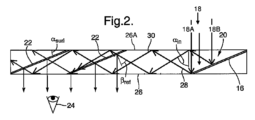
ここで、典型的な導光光学素子(LOE)の側面図である図2を参照する。上記の制限を緩和するために、選択反射面のアレイを、導光光学素子(LOE)内で使用し、製造することができる。第1の反射面(16)は、デバイスの後ろに位置決めされる光源(図示せず)から発せられるコリメートされた表示光線(入射光線ビーム)(18)により照射される。図面の簡潔さのために、1つの光線、すなわち、入射光線(18)(「ビーム」あるいは「入射光線」とも呼ばれる)だけが一般的に描かれている。ビーム(18A)と(18B)などの入射光の他の光線が入射光瞳の左と右の縁などの入射瞳の縁を指定するために使用されることもある。一般に、画像が光線によって本明細書に表される場合はいつでも、光線は画像のサンプルビームであり、これは、画像の点またはピクセルに各々対応するわずかに異なる角度にある複数のビームによって典型的に形成されることに留意されたい。特に画像の末端と呼ばれるところを除いて、例示されるビームは典型的に画像の重心である。 Reference is now made to FIG. 2, which is a side view of a typical light guiding optical element (LOE). To alleviate the above limitations, arrays of selectively reflective surfaces can be used and fabricated within light guiding optical elements (LOEs). The first reflective surface (16) is illuminated by a collimated display light beam (incident light beam) (18) originating from a light source (not shown) positioned behind the device. For simplicity of the drawing, only one ray, namely the incident ray (18) (also referred to as "beam" or "incident ray"), is generally drawn. Other rays of the incident light, such as beams (18A) and (18B), may also be used to specify the edges of the entrance pupil, such as the left and right edges of the entrance optical pupil. In general, whenever an image is represented herein by a ray, the ray is a sample beam of the image, typically by multiple beams at slightly different angles, each corresponding to a point or pixel in the image. Note that it is formed in The illustrated beam is typically the center of gravity of the image, except where specifically referred to as the edges of the image.
反射面(16)は、典型的には100%反射(完全なミラー)であり、光源からの入射光を反射し、入射光は内部全反射によって導光体(20)の内部で捕捉される。導光体(20)は「平面基板」、および「光送信基板」とも呼ばれる。導光体(20)は、第1の(後方の、主な)表面(26)と第2の(前方の、主な)表面(26A)として図面で示されている、互いに平行な少なくとも2つの(主)表面を含む。主表面(26、26A)に関して「第1の」および「第2の」という指定は参照の利便性のためのものであることに留意されたい。導光体へのカップリングイン(Coupling-in)は、前方、後方、側端などの、または他のあらゆる所望のカップリングイン幾何学の、様々な表面からでありえる。 The reflective surface (16) is typically 100% reflective (perfect mirror) and reflects the incident light from the light source, which is captured inside the light guide (20) by total internal reflection. . The light guide (20) is also called a "plane board" and a "light transmitting board." The light guide (20) has at least two parallel surfaces, shown in the drawings as a first (back, main) surface (26) and a second (front, main) surface (26A). Contains two (main) surfaces. Note that the designations "first" and "second" with respect to major surfaces (26, 26A) are for convenience of reference. Coupling-in to the light guide can be from various surfaces, such as the front, back, side edges, or any other desired coupling-in geometry.
入射光光線(18)は、基板の近位端(図の右側)で基板に入る。光は、導光体と1つ以上のファセット、通常少なくとも複数のファセット、および典型的にはいくつかの、3または4より多いファセットを通って、導光体の遠位端(図の左側)に向かって伝播する。光は、伝播の最初に反射された伝播方向(28)と別の伝播方向(30)の両方において導光体を通って伝播する。 The incident light ray (18) enters the substrate at its proximal end (right side of the figure). Light passes through the light guide and one or more facets, usually at least more than one facet, and typically several, more than three or four facets, to the distal end of the light guide (left side of the figure). propagate towards. Light propagates through the light guide both in the initially reflected propagation direction (28) and in another propagation direction (30).
捕捉された光は、基板(20)の内面から反射し、そして選択反射面のアレイ(22)を横断するように、導光体を介して、伝播する。選択反射面(22)は典型的には部分的に反射するカップリングアウト(coupling-out)・ファセットであり、それらの各々は、基板からビューアーの目(24)へと光の一部を結合する。 The captured light reflects from the inner surface of the substrate (20) and propagates through the light guide across the array of selectively reflective surfaces (22). The selectively reflective surfaces (22) are typically partially reflective coupling-out facets, each of which couples a portion of the light from the substrate to the viewer's eye (24). do.
選択反射面(22)などの内部の部分反射面は、本明細書の文脈では一般に「ファセット」と呼ばれる。現実用途の強化のために、ファセットは部分反射型であり、現実世界からの光が前面(26A)を介して入り、ファセットを含む基板を横断し、および、基板を出て背面(26)を介してビューアーの目(24)に至ることを可能にする。ファセットが部分反射型であることはまた、伝播光の一部が後に続くファセットに伝播し続けることを可能にする。内部の部分反射面(22)は一般に、導光体(20)の伸長の方向に対して斜角(つまり、平行でも垂直でもない)で導光体(20)を少なくとも部分的に横断する。部分反射は、限定されないが、ある割合の光の伝送、および/または偏光の使用を含む、様々な技術によって実行可能である。 Internal partially reflective surfaces, such as selectively reflective surfaces (22), are generally referred to as "facets" in the context of this specification. For enhanced real-world applications, the facets are partially reflective so that light from the real world enters through the front surface (26A), traverses the substrate containing the facets, and exits the substrate through the back surface (26). to the viewer's eyes (24). The partially reflective nature of the facets also allows some of the propagating light to continue propagating to subsequent facets. The internal partially reflective surface (22) generally at least partially traverses the light guide (20) at an oblique angle (ie, neither parallel nor perpendicular) to the direction of elongation of the light guide (20). Partial reflection can be performed by a variety of techniques including, but not limited to, transmission of a percentage of light and/or the use of polarization.
図3Aと図3Bは、選択反射面の所望の反射率挙動を例示する。図3Aでは、光線(32)はファセット(34)から部分的に反射され、基板(20)からカップルアウト(coupled out)される(38)。図3Bでは、光線(36)は顕著に反射されることなく、ファセット(34)を通って伝送される。 3A and 3B illustrate the desired reflectance behavior of a selectively reflective surface. In FIG. 3A, light ray (32) is partially reflected from facet (34) and coupled out (38) from substrate (20). In Figure 3B, the light ray (36) is transmitted through the facet (34) without being significantly reflected.
図4は、光を基板に結合させ、次にビューアーの目へと結合させる選択反射面のアレイの詳細な断面図である。ここで見られるように、光源(4)からの光線(18)は第1の反射表面(16)に衝突し、そして、反射光線(42)が内部全反射によって基板中へと結合される。捕捉された光線は、点(44)で他の2つの典型的な部分反射面(22)によって基板から徐々にカップルアウトされる。第1の反射面(16)の被膜特性は、他の反射面(22)、(46)の被膜特性に必ずしも類似しなければならないというわけではない。この被膜は、金属性、二色性、またはハイブリッドの金属-二色性の、完全反射型、または、ビームスプリッタであり得る。 FIG. 4 is a detailed cross-sectional view of an array of selectively reflective surfaces that couples light to the substrate and then to the viewer's eye. As seen here, the light beam (18) from the light source (4) impinges on the first reflective surface (16) and the reflected light beam (42) is coupled into the substrate by total internal reflection. The captured rays are gradually coupled out of the substrate by two other typical partially reflective surfaces (22) at point (44). The coating properties of the first reflective surface (16) do not necessarily have to be similar to the coating properties of the other reflective surfaces (22), (46). The coating can be metallic, dichroic, or hybrid metal-dichroic, fully reflective, or beam splitter.
図5は、標準的な眼鏡フレーム(107)に組み込まれたLOE(20a)/(20a’)および(20b)の一例を示している。表示光源(4)、折り畳み式の光学系、およびコリメート光学系(6)は、眼鏡フレームのアーム部分(112)の内部において、第2のLOE(20b)の縁部に位置決めされるLOE(20a)/(20a’)に隣接して、アセンブルされる。表示光源が小型のCRT、液晶ディスプレイ(LCD)、シリコン基板上の反射型液晶(LCoS)、デジタルマイクロミラーデバイス(DMD)、マイクロLEDアレイ、またはOLED、などの電子素子である場合は、表示光源の駆動電子機器(114)はアーム(112)の背面部分の内部にアセンブルされ得る。電源およびデータインターフェース(116)は、リード(118)、または無線または光の伝送を含む他の通信手段によってアーム(112)に接続可能である。代替的に、バッテリーおよび小型データリンク電子機器は、眼鏡フレームにおいて一体化され得る。本図は一例であり、表示光源が、LOE平面と平行に、またはLOEの前方部分において取り付けられる、アセンブリを含む、他の考えられ得るヘッドマウントディスプレイの配置も構築され得る。 Figure 5 shows an example of LOE (20a)/(20a') and (20b) incorporated into a standard eyeglass frame (107). The display light source (4), the folding optics and the collimating optics (6) are located at the edge of the second LOE (20b) within the arm portion (112) of the eyeglass frame. )/(20a'). If the display light source is an electronic device such as a small CRT, liquid crystal display (LCD), reflective liquid crystal on silicon substrate (LCoS), digital micromirror device (DMD), microLED array, or OLED, the display light source The drive electronics (114) may be assembled inside the back portion of the arm (112). A power and data interface (116) can be connected to the arm (112) by a lead (118) or other communication means including wireless or optical transmission. Alternatively, the battery and small data link electronics may be integrated in the eyeglass frame. This figure is an example, and other possible head-mounted display arrangements may also be constructed, including assemblies in which the display light source is mounted parallel to the LOE plane or in the anterior portion of the LOE.
この基礎技術のさらなる詳細は米国特許第7,643,214号において見ることができる。 Further details of this basic technology can be found in US Pat. No. 7,643,214.
図6は、部分反射面のアレイを製作する方法を例示する。複数の透明な平たいプレート((422R)、5つの典型的なプレート(S1)から(S5)として示される)の表面は、必要なコーティング(440)をほどこされ、次に、プレート(S1からS5)は、スタック形態(442)を成すように接合される。その後、セグメント(444)は、反射表面(446)の所望のアレイを生じるために、切断、研削、および研磨によってスタック形態からスライスされ、その後、それはLOEの全体を実現するために他の構成要素とアセンブルされ得る。コーティングされたプレート(S1からS5)の実際の寸法とLOEの必要な寸法に従って、個々のセグメント(444)から1つを超えるアレイ(446)が製作され得る。 FIG. 6 illustrates a method of fabricating an array of partially reflective surfaces. The surfaces of a plurality of transparent flat plates ((422R), shown as five typical plates (S1) to (S5)) are applied with the necessary coatings (440) and then the plates (S1 to S5 ) are joined to form a stacked configuration (442). The segment (444) is then sliced from the stacked form by cutting, grinding, and polishing to yield the desired array of reflective surfaces (446), after which it is assembled with other components to realize the entire LOE. can be assembled with. More than one array (446) may be fabricated from individual segments (444) according to the actual dimensions of the coated plates (S1 to S5) and the required dimensions of the LOE.
図7は選択反射面のアレイを製作するための方法のさらなる詳細である。スライスされた導光体(446)は、例えば、両側面に沿って、導光体の近位端となる破線(420A)に沿って、および、導光体の遠位端となる破線(420B)に沿って、垂直にカットされる。これにより、導光体(420)がもたらされる。随意に、導光体(424)と(426)は、導光体(420)の近位端および遠位端にそれぞれ貼り付けられ、そしてその組合せ((420)、(424)、および(426)の)は導光体(LOE)(429)を製造するために研磨される。あるいは、端のプレート(S1とS5)は間のプレート(S2、S3、S4)より厚くすることができ、結果として、スライスされた導光体(446)の構造は、導光体(424)と(426)を貼り付けられた領域が端のプレート(S1とS5)に由来しながら、導光体(429)に類似したものとなる。 FIG. 7 provides further details of the method for fabricating an array of selectively reflective surfaces. The sliced lightguide (446) is cut, for example, along both sides, along a dashed line (420A) that represents the proximal end of the lightguide, and along a dashed line (420B) that represents the distal end of the lightguide. ) is cut vertically. This results in a light guide (420). Optionally, lightguides (424) and (426) are affixed to the proximal and distal ends of lightguide (420), respectively, and the combination ((420), (424), and (426) ) is polished to produce a light guide (LOE) (429). Alternatively, the end plates (S1 and S5) can be thicker than the intervening plates (S2, S3, S4), so that the structure of the sliced lightguide (446) is similar to that of the lightguide (424). The area to which (426) is attached originates from the end plates (S1 and S5), but resembles the light guide (429).
一般に、もとの透明な平たいプレート(422R)の各々は、1組のコーティングされたプレート(422)のプレートを結果としてもたらす。プレート(422)の各々は3ペアの面を有し、面のペアの各々は、プレートの平行な外面である。1ペアの面(本図中の左および右の側面として示される)は、導光体(LOE)の長軸を形成するために、被覆され、隣接するプレートに接合される。その後、別のペアの面(本図中、最上部および底部に示される「端」)は、主要外面(前面(26A)と背面(26)を含む)を形成するようにそれぞれ研削され、および研磨される。コーティングされたプレートの組は、プレートが対面するところに作成されたファセットを含み、従って、プレートの組はファセットの組を含む。ファセットの組は、主要外面(26A、26)のペアの間において、互いに対して平行であり、および、主要外面(26A、26)に対して平行ではない角度にある。 Generally, each original transparent flat plate (422R) results in a set of coated plates (422). Each of the plates (422) has three pairs of faces, each pair of faces being parallel outer faces of the plate. A pair of faces (shown as left and right sides in this figure) are coated and bonded to adjacent plates to form the long axis of the light guide (LOE). Thereafter, another pair of surfaces (the "edges" shown at the top and bottom in this figure) are each ground to form the major outer surfaces (including the front surface (26A) and the back surface (26)), and Polished. The set of coated plates includes facets created where the plates face each other, and thus the set of plates includes a set of facets. The sets of facets are parallel to each other and at angles not parallel to the major exterior surfaces (26A, 26) between the pair of major exterior surfaces (26A, 26).
本図はオーバーラップしないファセットを有するLOEを示しているが、これに制限されず、二重オーバーラップ、および、三重オーバーラップなどのオーバーラップするファセット(図示せず、2018年1月8日に出願されたPCT/IL2018/050025を参照し、その全体は参照によって本明細書に組み入れられる)に、本発明の実施例を適用することもできる。 Although this figure shows a LOE with non-overlapping facets, it is not limited to this and includes overlapping facets such as double overlap and triple overlap (not shown, as of January 8, 2018). Embodiments of the present invention may also be applied to PCT/IL2018/050025, which is incorporated herein by reference in its entirety.
詳細な説明-第1の実施形態図8から図15
ここで、LOE導光体(20)に対する試験の典型的な部分の見取図である図8を参照する。この典型的な実施例は、図2に関連して上に記載されるようにLOEを使用する。作業において、入射光線(18)は近位端(54)においてLOE(20)に進入することができる。本試験構成において、当該技術分野において知られているように試験用光線を発生させるために、表示光源(804)はコリメート光学系(806)に光を出力するが、そのことは投影光(R)の試験光線として示されている。試験光線(投影光(R))はコリメートされ得るが、典型的には厳密にコリメートされるのではなく、試験用の投影光(R)を発生させるためにわずかに焦点をぼかされる。試験は、好ましくは単色光(すなわち、光の単一波長)を用いて行われるが、典型的に可視スペクトルにおけるどの波長でも行なうことができる。この実施例は制限するものではなく、例えば、赤外線などの他の波長も使用することができる。オリエンテーションについては、本図において、前面(26A)は入射光線(R)に向かっており、典型的には下記の図(図9から図10B)において示されるような角度にある。この場合、入射光線は、LOE(20)の前面(26A)に対して下向きの角度で、ページの外から到来している。投影光(R)は、図において示されるように、典型的には前面(26A)に対して斜角で、前面(26A)に向かって投影される。この典型的な実施例は制限するものではなく、投影光(R)は、代替的に、前面(26A)に対して垂直に前面(26A)に向かって投影されてもよい。
Detailed Description - First Embodiment Figures 8 to 15
Reference is now made to FIG. 8, which is a sketch of a typical portion of a test on a LOE lightguide (20). This exemplary embodiment uses LOE as described above in connection with FIG. In operation, an incident light beam (18) may enter the LOE (20) at the proximal end (54). In this test configuration, the display light source (804) outputs light to the collimating optics (806) to generate a test beam as is known in the art, which means that the projection light (R ) is shown as the test ray. The test light beam (projection light (R)) may be collimated, but is typically not strictly collimated, but slightly defocused to generate the test projection light (R). Testing is preferably performed using monochromatic light (ie, a single wavelength of light), but can typically be performed at any wavelength in the visible spectrum. This example is not limiting; other wavelengths can also be used, for example infrared. Regarding orientation, in this figure the front surface (26A) is towards the incident ray (R) and is typically at an angle as shown in the figures below (Figures 9-10B). In this case, the incident rays are coming from outside the page at a downward angle to the front surface (26A) of the LOE (20). Projection light (R) is projected toward the front surface (26A), typically at an oblique angle to the front surface (26A), as shown in the figure. This exemplary embodiment is not limiting, and the projection light (R) may alternatively be projected perpendicularly to the front surface (26A) towards the front surface (26A).
屈折/反射光線(R’)および外部で反射された光線(Re’)は、前面(26A)から離れてページの外へ、上向きの角度で伝播する。このことは、図9中の試験構成(900)(以下に記載される)を見ることによって一層よく理解され得る。 The refracted/reflected ray (R') and the externally reflected ray (Re') propagate at an upward angle away from the front surface (26A) and out of the page. This can be better understood by looking at the test configuration (900) in FIG. 9 (described below).
試験光線(R)は典型的な試験光線(R1)から(R7)としての示されており、それらは各々(R1’)から(R7’)として示される典型的な屈折/反射光線(R’)として、LOEを横断して外に出る。LOE導光体(20)は、主要な表面(前面(26A)および背面(26))の間に、ファセット(22)を含み、それらは二重線で示されている。屈折/反射光線(R1’)から(R7’)の経路は明確性のために単純化されていることに留意されたい。以下に記載されるように、ファセット(22)における屈折/反射光線(R’)の光路長の各々は、ファセットのいずれかの側にあるプレート間での不整合(不均一性)により変化するだろう。 The test rays (R) are shown as typical test rays (R1) to (R7), which are typical refracted/reflected rays (R') shown as (R1') to (R7'), respectively. ), cross the LOE and exit. The LOE lightguide (20) includes facets (22) between the major surfaces (front (26A) and back (26)), which are shown with double lines. Note that the path of the refracted/reflected rays (R1') to (R7') has been simplified for clarity. As described below, the optical path length of each refracted/reflected ray (R') at a facet (22) varies due to misalignment (non-uniformity) between the plates on either side of the facet. right.
試験光線(R)は外面(前面26A)によっても、外部で反射された光(Re’)として反射されるであろう。明確性のために、外部で反射された光(R7e’)の典型的な光線が1つだけ本図中に示される(明確性のために、明らかに、正確な反射角ではない)。
The test ray (R) will also be reflected by the outer surface (
本図において、第1の屈折率n1を有する典型的なプレート-1 (S1)、第2の屈折率n2を有するプレート-2 (S2)、第3の屈折率n3を有するプレート-3 (S3)、第4の屈折率n4を有するプレート-4 (S2)、第5の屈折率n5を有するプレート-5 (S2)、および、第6の屈折率n6を有するプレート-6 (S2)、を含む、プレート(422)が示される。また、典型的なファセットも示される:プレート-1( S1)とプレート-2(S2)の間のファセット(F12)、プレート-2(S2)とプレート-3(S3)の間のファセット(F23)、プレート-3(S3)とプレート-4(S4)の間のファセット(F34)、プレート-4(S4)とプレート-5(S5)の間のファセット(F45)、および、プレート-5(S5)とプレート-6(S6)の間のファセット(F56)。あるいは、プレートはファセット間にあると記載することができ、例えば、プレート-2(S2)はファセット(F12)とファセット(F23)の間にある。 In this figure, a typical plate-1 (S1) with a first refractive index n 1 , a plate-2 (S2) with a second refractive index n 2 , a plate-2 with a third refractive index n 3 3 (S3), a plate-4 (S2) having a fourth refractive index n 4 , a plate-5 (S2) having a fifth refractive index n 5 , and a plate-4 having a sixth refractive index n 6 . 6 (S2), a plate (422) is shown. Also shown are typical facets: facet between plate-1 (S1) and plate-2 (S2) (F12), facet between plate-2 (S2) and plate-3 (S3) (F23). ), facet (F34) between plate-3 (S3) and plate-4 (S4), facet (F45) between plate-4 (S4) and plate-5 (S5), and plate-5 ( S5) and the facet (F56) between plate-6 (S6). Alternatively, the plates can be described as being between facets, eg plate-2 (S2) is between facet (F12) and facet (F23).
理想的には、各々のプレートの屈折率は一致するべきであり、すなわち、屈折率は均一なはずである:n1=n2=n3=n4=n5=n6。しかしながら、実際には、典型的に1つ以上の屈折率の間にいくらかの偏差がある。典型的な場合では、第1の群(n1、n2、n4、n6)はすべて、異なる屈折率を有し、および、第2の群(n3、n5)は両方とも第1の群の屈折率とは異なる同一の屈折率を有する。この場合、試験光線(R1)は、屈折率n2を有するプレート-2(S2)を介してLOEの20%を横断し、屈折率n3を有するプレート-3 (S3)を介して80%(残りの幅)を横断するようにファセット(F23)で屈折し、屈折率n3を有するプレート-3 (S3)を介してLOEの80%を横断する屈折/反射光線(R1’)として、背面(26)から反射し、屈折率n2を有するプレート-2 (S2)を介してLOEの幅の残り20%を横断するように、ファセット(F23)で屈折し、および、前面(26A)を介してLOEから出るであろう。 Ideally, the refractive index of each plate should match, ie, the refractive index should be uniform: n 1 = n 2 = n 3 = n 4 = n 5 = n 6 . However, in reality there is typically some deviation between one or more refractive indices. In a typical case, the first groups (n 1 , n 2 , n 4 , n 6 ) all have different refractive indices, and the second groups (n 3 , n 5 ) both have different refractive indices. have the same refractive index different from that of the first group. In this case, the test ray (R1) traverses 20% of the LOE through plate-2 (S2) with refractive index n 2 and 80% through plate-3 (S3) with refractive index n 3 . As the refracted/reflected ray (R1') refracts at the facet (F23) to traverse (remaining width) and traverses 80% of the LOE via plate-3 (S3) with refractive index n 3 , reflected from the back surface (26) and refracted at the facet (F23) to traverse the remaining 20% of the width of the LOE via plate-2 (S2) with a refractive index n 2 ; and the front surface (26A). will exit the LOE via.
同様に、試験光線(R2)~(R7)は、それぞれ以下のような反射光線(R2’)~(R7’)としてLOEを横断するであろう(各々のプレートについて括弧中に対応する屈折率、1つの方向だけが記載される):
(R2)は100%がプレート-3(S3)(n3)を介する(R2’)として、
(R3)は80%がプレート-3(S3)(n3)を介し、20%がプレート-4(S4)(n4)を介する、(R3’)として、
(R4)は50%がプレート-3(S3)(n3)を介し、50%がプレート-4(S4)(n4)を介する(R4’)として、
(R5)は20%がプレート-3(S3)(n3)を介し、80%がプレート-4(S4)(n4)を介する(R5’)として、
(R6)は100%がプレート-4(S4)(n4)を介する(R6’)として、および
(R7)は100%がプレート-5(S5)(n5)を介する(R7’)として。
Similarly, test rays (R2) to (R7) will traverse the LOE as reflected rays (R2') to (R7'), respectively (with corresponding refractive index in parentheses for each plate). , only one direction is listed):
Assuming that (R2) is 100% mediated by plate-3 (S3) (n 3 ) (R2'),
(R3) is 80% via plate-3 (S3) (n 3 ) and 20% via plate-4 (S4) (n 4 ), as (R3'),
Assuming that (R4) is 50% via plate-3 (S3) (n 3 ) and 50% via plate-4 (S4) (n 4 ) (R4'),
Assuming that (R5) is 20% via plate-3 (S3) (n 3 ) and 80% via plate-4 (S4) (n 4 ) (R5'),
(R6) as (R6') with 100% via plate-4 (S4) (n 4 ), and (R7) as (R7') with 100% via plate-5 (S5) (n 5 ). .
n3=n5であるこの場合において、試験光線(R2)と(R7)(および対応する屈折/反射光線(R2’)と(R7’)は)の有効光路長は、およびそれ故に、前面(26A)から反射された光線の部分と背面(26)から反射された光線の部分との間の位相差は相似するはずである。しかしながら、試験光線(R2)から(R6)の光路長および結果として生じる位相差は、不均一な基板(プレート)の割合が変化するに従って変化するはずである。 In this case where n 3 = n 5 , the effective optical path length of the test rays (R2) and (R7) (and the corresponding refracted/reflected rays (R2') and (R7')) is, and therefore The phase difference between the portion of the ray reflected from (26A) and the portion of the ray reflected from the back surface (26) should be similar. However, the optical path length and the resulting phase difference of the test beams (R2) to (R6) should change as the proportion of non-uniform substrates (plates) changes.
ここで、典型的な試験構成の高水準の側面見取り図である図9を参照する。試験構成(900)は、試験のための典型的な構成を示す。図中の明確性のために、外部で反射された光(Re’)は二点鎖線を用いて示され、および屈折/反射光線(R’)は点線を用いて示される。表示光源(804)は試験光線(R)を発生させるためにコリメート光学系(806)に光を出力する。屈折/反射光線(R’)はLOE(20)から出力され、および、キャプチャデバイス(1002)によって受信される。外部で反射された光(Re’)はLOE(20)の外面から反射され、キャプチャデバイス(1002)によって受信される。キャプチャデバイス(1002)は、屈折/反射光線(R’)と外部で反射された光(Re’)との間で生じた干渉信号の画像を捕捉する。利便性上、屈折/反射光線R’から生じ、かつキャプチャデバイス(1002)によってキャプチャされるインターフェログラム画像は、この記載においてインターフェログラムと呼ばれ、以下に説明されるように、波動干渉によって形成されたパターンが特に写真またはダイヤグラムにおいて表現される。 Reference is now made to FIG. 9, which is a high level side view of a typical test configuration. Test configuration (900) shows a typical configuration for testing. For clarity in the figures, externally reflected light (Re') is shown using dash-dotted lines, and refracted/reflected rays (R') are shown using dotted lines. The display light source (804) outputs light to collimating optics (806) to generate a test beam (R). A refracted/reflected ray (R') is output from the LOE (20) and received by the capture device (1002). Externally reflected light (Re') is reflected from the outer surface of the LOE (20) and received by the capture device (1002). A capture device (1002) captures an image of the interference signal generated between the refracted/reflected light beam (R') and the externally reflected light (Re'). For convenience, the interferogram image resulting from the refracted/reflected ray R' and captured by the capture device (1002) is referred to in this description as an interferogram, and as explained below, the interferogram image is The formed pattern is particularly represented in a photograph or diagram.
干渉パターンはプレート(422)間における屈折率の不均一性を測定するために用いられる。干渉パターンは屈折/反射光線(R’)と外部で反射された光(Re’)との間のものである。屈折/反射光線(R’)は、投影光(R)が導光体(20)を横断し、内部反射し、次に、前面(26A)を介して外に出た結果である。外部で反射された光(Re’)は、投影光(R)が前面(26A)から反射される結果である。 The interference pattern is used to measure the refractive index non-uniformity between the plates (422). The interference pattern is between the refracted/reflected ray (R') and the externally reflected light (Re'). The refracted/reflected ray (R') is the result of the projection light (R) traversing the light guide (20), being internally reflected, and then exiting through the front surface (26A). The externally reflected light (Re') is the result of the projection light (R) being reflected from the front surface (26A).
特定の所望の試験のために便利かつ適切であるように、キャプチャデバイスは様々な実施例を含み得る。例えば、干渉信号(光線(R’)、(Re’))はスクリーン上に投影され、および、結果として生じるインターフェログラムの写真を撮るために手持ち式カメラが使用される。別の例において、CCD(電荷結合素子)は直接光線(R’、Re’)の干渉をキャプチャするように設置することができる。インターフェログラムは処理モジュール(1004)によって随意に記憶され、処理される。 The capture device may include a variety of embodiments as convenient and appropriate for the particular desired test. For example, the interference signals (rays (R'), (Re')) are projected onto a screen, and a handheld camera is used to take a picture of the resulting interferogram. In another example, a CCD (charge-coupled device) can be placed to capture the interference of the direct beam (R', Re'). The interferogram is optionally stored and processed by a processing module (1004).
ここで、干渉縞がどのように形成されるかを側面視で説明した図10Aを参照する。干渉縞は、参照光線(投影される試験光線(R))が第1のLOE(20)の前面(26A)から反射し(外部で反射された光(Re’))、対応する屈折/反射光線(R’)(それはLOE(20)内へと進み、背面(26)から反射する)と干渉し、その後、LOE(20)をスクリーン(キャプチャデバイス(1002))に対して、形成される。本図において、参照試験光線(R)の典型的な部分は第1の部分(Ra)と第2の部分(Rb)として示される。第1の部分(Ra)は、LOE(20)を横断し、反射し、屈折して、および反射光線(Ra’)として外に出る。第2の部分(Rb)は、外部で反射された光線(Rb’)としてLOE(20)の外部前面(26a)で反射される。(自動)コリメーター・システムから出る光線(試験光線R)の焦点が、わずかにぼかされる時、干渉縞が観察される。コリメーター(806)の焦点をぼかすことは、干渉縞の偏差の相対変化に影響しない。コリメーター(806)の焦点をより少ししかぼかさなかった場合、結果としてより遠く離れた相対的に少ない干渉縞をもたらすが、それに比較して、コリメーター(806)の焦点をより大幅にぼかすことは、結果として干渉縞を互いにより密にするだろう。コリメーターの焦点がぼかされなければ、結果として生成されるインターフェログラムは単一の干渉縞、すなわち、すべてが1つの明度になるだろう。一般に、コリメーター(806)は、干渉縞の飛びを識別するために十分な干渉縞を観察するために、十分に調節される(焦点をずらされる)が、干渉縞の数が増加して互いにより接近するほどには調節され(焦点をずらされ)過ぎることはなく、干渉縞の形状(それらの形態)において変化が認識可能になるだろう。一般的には、導光体(20)の外面(前面(26A)と背面(26))は、高い精度に機械加工され、および、干渉縞の一因とはならない。 Here, reference is made to FIG. 10A, which illustrates how interference fringes are formed in a side view. The interference fringes are generated when the reference beam (projected test beam (R)) is reflected from the front surface (26A) of the first LOE (20) (externally reflected light (Re')) and the corresponding refraction/reflection occurs. Interfering with the ray (R'), which travels into the LOE (20) and reflects from the back surface (26), the LOE (20) is then formed against the screen (capture device (1002)). . In this figure, typical parts of the reference test beam (R) are shown as a first part (Ra) and a second part (Rb). The first portion (Ra) traverses the LOE (20), is reflected, refracted, and exits as a reflected ray (Ra'). The second portion (Rb) is reflected at the external front surface (26a) of the LOE (20) as an externally reflected ray (Rb'). When the light beam (test beam R) emerging from the (automatic) collimator system is slightly defocused, interference fringes are observed. Defocusing the collimator (806) does not affect the relative change in fringe deviation. Defocusing the collimator (806) less results in relatively fewer interference fringes that are farther apart, compared to defocusing the collimator (806) more significantly. will result in the interference fringes being closer together. If the collimator were not defocused, the resulting interferogram would be a single interference pattern, ie, all of one brightness. Generally, the collimator (806) is sufficiently adjusted (defocused) to observe enough interference fringes to identify fringe jumps, but the number of interference fringes increases and The closer it gets, the less it will be adjusted (defocused) and a change in the shape of the interference fringes (their morphology) will become discernible. Typically, the outer surfaces of the light guide (20) (front (26A) and back (26)) are machined to high precision and do not contribute to interference fringes.
参照のために、図8の光線(R1)から(R7)は、図10Aにおいて描かれるようにページへ「積み重ね」られ、ここで、本図10A中のLOE(20)の姿は、図8のLOE(20)の左側からのものである。 For reference, rays (R1) to (R7) of FIG. 8 are "stacked" onto the page as depicted in FIG. 10A, where the appearance of LOE (20) in this FIG. This is from the left side of LOE (20).
ここで干渉の詳細な見取り図である図10Bを参照する。スクリーン(キャプチャ画像)上の信号の外観は、本図の光線のうち外部で反射された光線(Re’)(二点鎖線)と反射/屈折光線(R’)(破線)の間の光路長差の指標である。本図は、空気とS-TIM8ガラス(n= 1.5955)との間の界面における屈折の一例であり、従って、LOE(20)内部の屈折角は26.3度である。 Reference is now made to FIG. 10B, which is a detailed sketch of the interference. The appearance of the signal on the screen (captured image) is the optical path length between the externally reflected ray (Re') (dashed line) and the reflected/refracted ray (R') (dashed line) in this figure. It is an indicator of difference. This figure is an example of refraction at the interface between air and S-TIM8 glass (n=1.5955), so the refraction angle inside LOE (20) is 26.3 degrees.
ここで、LOEの様々な範囲についての全体的なパターンの発生の見取り図である図11を参照する。干渉縞パターンが、LOE(20)を通り抜けない光(外部で反射された光(Re’))とLOE(20)を通り抜ける光(屈折/反射光線(R’))との間の干渉を含むため、全体のパターンは、LOE(20)の様々な範囲(すなわち異なるプレート)を通り抜ける光線について比較情報を明らかにする。本図において、プレート(S11)、(S12)、(S13)はそれぞれの屈折率(n1、n2、n1)を有する。このことは、本図において描写されており、ここで、光線路(1101)と光線路(1102)は潜在的に異なる屈折率を有する異なるプレートを通ってLOE(20)を横断する。本図はこれらの光線(1101、1102)を示す。先の図10Bの方向付けにおいて、光線路(1101)と光線路(1102)はオーバーラップし、および、反射/屈折光線(R’)として示される。結果として生じるインターフェログラム(1200)は、外部で反射された光線(Re’)と反射/屈折(1101)/(1102)光線との間の光路差を、帯(B)として、または、黒い若しくは暗い領域(D)の間の「縞」として示す。典型的な3つの帯(B1)、(B2)、(B3)は、4つの典型的な暗い領域(D1)、(D2)、(D3)、(D4)の間に示される。ヘリウム~ネオンの赤いレーザ源が用いられる場合、帯Bは暗い領域(D)の間の赤色となるだろう。その代わりに、本図の黒い領域(D)と白色の縞(B)のように、グレイスケールまたは白黒の画像が用いられてもよい。 Reference is now made to FIG. 11, which is a sketch of the overall pattern development for various ranges of LOE. The interference fringe pattern includes interference between light that does not pass through the LOE (20) (externally reflected light (Re')) and light that passes through the LOE (20) (refracted/reflected rays (R')) Therefore, the overall pattern reveals comparative information about the rays passing through different regions (ie different plates) of the LOE (20). In this figure, plates (S11), (S12), and (S13) have respective refractive indices (n 1 , n 2 , n 1 ). This is depicted in this figure, where the optical path (1101) and the optical path (1102) traverse the LOE (20) through different plates with potentially different refractive indices. The figure shows these rays (1101, 1102). In the previous orientation of FIG. 10B, the rays (1101) and rays (1102) overlap and are shown as reflected/refracted rays (R'). The resulting interferogram (1200) shows the optical path difference between the externally reflected ray (Re') and the reflected/refracted (1101)/(1102) rays as a band (B) or as a black or as "stripes" between dark areas (D). Three typical bands (B1), (B2), (B3) are shown between four typical dark areas (D1), (D2), (D3), (D4). If a helium to neon red laser source is used, band B will be red between the dark regions (D). Alternatively, a gray scale or black and white image may be used, such as the black areas (D) and white stripes (B) in this figure.
干渉縞(帯B)は、インターフェログラムの暗い領域の中心から、可視光線領域を通って、再び次の暗い範囲の中心に延在する範囲である。例えば、縞(B1)は、暗い領域(D1)と暗い領域(D2)間の光の範囲である。光の範囲は、2つの別個の経路からの光線が一致し、および互いに同位相である時に生じる。すなわち、光線の光路長は波長の整数によって区切られ、および、強め合う干渉が生じる。従って、ある範囲で2つの別個の進路から光線が一致し、互いに位相が異なる場合、すなわち、(n+1/2)波長によって区切られて、弱め合う干渉が生じて、範囲は暗くなる。従って、結果として生じた干渉縞パターンはLOE中の相対的な光路長の直接の指標であり、それは次には屈折率の変化の指標である。 The interference fringes (band B) are the range extending from the center of the dark region of the interferogram through the visible light region and back to the center of the next dark region. For example, a stripe (B1) is a range of light between a dark area (D1) and a dark area (D2). A range of light occurs when the light rays from two separate paths coincide and are in phase with each other. That is, the optical path length of the light beam is bounded by an integer number of wavelengths, and constructive interference occurs. Thus, if in a range light rays from two separate paths coincide and are out of phase with each other, ie separated by (n+1/2) wavelengths, destructive interference will occur and the range will be darkened. The resulting fringe pattern is therefore a direct indicator of the relative optical path length during the LOE, which in turn is an indicator of the change in refractive index.
本図において、干渉縞は、全般において水平の帯であり、LOE(20)の長軸に沿ったアライメントに対応している。2つのスロープが示される:スロープ(1130)はLOE(20)のプレート(S11)と(S12)の領域に対応し、および、スロープ(1132)はLOE(20)のプレート(S12)とプレート(S13)の領域に対応する。インターフェログラム(1200)中のスロープは、光線路(反射/屈折光線(R’)、図8への参照において記載されたように)が、2枚のプレート間で徐々に分割される(本図中の(n1)と(n2)の比率を変化させながら)領域を表現する。(1211)とマークされた線は、(n1)の特性を決定する(プレート(S11)は屈折率(n1)を有し、ここで光線は100%プレート(S11)を介して、つまり100%(n1)の、LOEを横断する)。同様に、(1212)とマークされた線は、(n2)の特性を決定する(プレート(S12)は屈折率(n2)を有し、ここで、屈折/反射光線は100% プレート(S12)を介して、つまり100%(n2)の、LOEを横断する)。 In this figure, the interference fringes are generally horizontal bands, corresponding to alignment along the long axis of LOE (20). Two slopes are shown: slope (1130) corresponds to the area of plates (S11) and (S12) of LOE (20), and slope (1132) corresponds to the area of plates (S12) and (S12) of LOE (20). This corresponds to the area S13). The slope in the interferogram (1200) indicates that the optical path (reflected/refracted ray (R'), as described in reference to FIG. The area is expressed by changing the ratio of (n 1 ) and (n 2 ) in the figure. The line marked (1211) determines the properties of (n 1 ) (the plate (S11) has a refractive index (n 1 ), where the ray passes 100% through the plate (S11), i.e. 100% (n 1 ) across the LOE). Similarly, the line marked (1212) determines the properties of (n 2 ) (plate (S12) has a refractive index (n 2 ), where the refracted/reflected rays are 100% of the plate ( S12), i.e. 100% (n 2 ) of the LOE).
プレート(S11、S12、S13)の屈折率の間に違いがあるならば、光線(1101)/(1102)は異なる光路長(OPL)を有し、および、位相の変化は干渉縞パターン中の偏差に反映されるだろう。プレート(典型的には隣接した)の特性間におけるこの差異は「干渉縞の飛び」と呼ばれる。干渉縞飛びは、干渉縞の第1の水平の場所での1つの部分と干渉縞の別の水平の場所での別の部分の間の垂直の差によって、インターフェログラム(1200)において見ることができる。非限定的な一例は、干渉縞飛び(1114)を有する典型的な干渉縞(B2)に見ることができる。一般に、干渉縞(干渉縞の寸法、干渉縞の幅)はすべて、干渉縞の寸法(1116)によって示されるものと同じ寸法になるだろう。一般に、干渉縞寸法と干渉縞の飛びは、例えば、暗い領域(D)の中間点または干渉縞(B)の中間点からなど、干渉縞におけるどの点からでも測定することができる。この例では、干渉縞飛び(1114)は、線(1211)において第1の点(1111)を有する第1の部分から、線(1212)において第2の点(1112)を有する第2の部分まで測定される。この場合、プレート(S11)からプレート(S12)までの光路長の差は、ほぼ干渉縞の縞1つ分の差(1つの縞(1116)の干渉縞飛び(1114))をもたらしている。 If there is a difference between the refractive indices of the plates (S11, S12, S13), the rays (1101)/(1102) will have different optical path lengths (OPL) and the change in phase will be due to the difference in the fringe pattern. This will be reflected in the deviation. This difference between the properties of (typically adjacent) plates is called "fringe jump." Fringe jump can be seen in the interferogram (1200) by the vertical difference between one portion of the interference fringe at a first horizontal location and another portion of the interference fringe at another horizontal location. I can do it. A non-limiting example can be seen in a typical fringe (B2) with fringe skip (1114). Generally, the interference fringes (fringe size, fringe width) will all have the same dimensions as indicated by fringe size (1116). In general, fringe size and fringe jump can be measured from any point in the fringe, such as from the midpoint of the dark region (D) or the midpoint of the fringe (B). In this example, the fringe jump (1114) is from a first portion having a first point (1111) at line (1211) to a second portion having a second point (1112) at line (1212). measured up to. In this case, the difference in optical path length from the plate (S11) to the plate (S12) brings about a difference of one interference fringe (interference fringe jump (1114) of one fringe (1116)).
典型的な計算として、1x10⁻⁴の不均一性がある隣接するプレートについての干渉縞の差異はいくらだろうか。 As a typical calculation, what is the difference in the interference fringes for adjacent plates with a 1x10 -4 inhomogeneity?
材料の内部の屈折角は、以下の式で計算され: The internal refraction angle of the material is calculated by the following formula:
そのとき、これらの隣接するプレート中の進路間における光路長の差は次のとおりだろう: The difference in optical path length between paths in these adjacent plates would then be:
式中、dはスライス厚み(LOE(20)の幅)、mは結果として生じた干渉縞飛びの数、および、λは試験光線(R)の波長である。 where d is the slice thickness (width of LOE(20)), m is the resulting number of fringe jumps, and λ is the wavelength of the test beam (R).
パラメーターとしては、n1=1.5955 n2=1.5956 d=1.5mm Δn=1・10-4
λ=632.8・10-9
→m=0.40
The parameters are: n 1 = 1.5955 n 2 = 1.5956 d = 1.5 mm Δn = 1・10 −4
λ=632.8・10 -9
→m=0.40
従って、1x10⁻⁴のプレートにおける屈折率の不均一性は0.40縞の干渉縞飛びとして現われるだろう。 Therefore, the non-uniformity of the refractive index in a 1×10 −4 plate will appear as a 0.40-fringe fringe skip.
ここで、好適な干渉縞パターンの写真である図12を参照する。本図において、インターフェログラムは、最大限の干渉縞飛びが0.3縞未満であることを示す。これは、1x10⁻⁴未満の不均一性を示す。 Reference is now made to FIG. 12, which is a photograph of a preferred interference fringe pattern. In this figure, the interferogram shows a maximum fringe jump of less than 0.3 fringes. This shows a non-uniformity of less than 1×10 −4 .
ここで、不良な干渉縞パターンの写真である図13を参照する。この一例において、「不良な」干渉縞パターンは、被測定デバイス(LOE(20))の特定の用途のために許容される最大値よりも大きな不均一性を示す。本図のインターフェログラムの左側に、ほとんど縞まるまる1つ分の干渉縞飛びが見られる。これは、およそ2x10⁻⁴の不均一性に相当する。 Reference is now made to FIG. 13, which is a photograph of a defective interference fringe pattern. In this example, a "bad" fringe pattern exhibits non-uniformity greater than the maximum allowed for the particular application of the device under test (LOE (20)). On the left side of the interferogram in this figure, an interference fringe skip of almost one entire fringe can be seen. This corresponds to a non-uniformity of approximately 2×10 −4 .
ここで、非常に不良な干渉縞パターンの写真である図14を参照する。この著しい不均一性は、この試験のLOE(20)を使用して見られるパターンの中に、一見してわかる飛びをもたらす。 Reference is now made to FIG. 14, which is a photograph of a very poor interference fringe pattern. This significant non-uniformity results in apparent jumps in the pattern seen using the LOE(20) of this test.
本図に描かれた垂直線(1400)はファセットの境界を表示する。点(1402)によって表示された干渉縞分離は最大限の不均一性を表現する。本インターフェログラムにおいて、6枚のプレートの各々は屈折率の顕著な差異を有する。最悪の場合、干渉縞飛びは縞まるまる2本分である(水平線(1404)間の干渉縞飛び(1406))。これは、およそ5x10⁻⁴の不均一性に相当する。 The vertical lines (1400) drawn in this figure indicate the boundaries of the facets. The fringe separation represented by point (1402) represents maximum non-uniformity. In this interferogram, each of the six plates has a significant difference in refractive index. In the worst case, the interference fringe jump is two whole fringes (interference fringe jump (1406) between the horizontal lines (1404)). This corresponds to a non-uniformity of approximately 5×10 −4 .
干渉縞飛びの決定
干渉縞の1つ以上の部分と干渉縞の別の1つ以上の部分の間の偏差を決定する工程は、プレートの屈折率間の屈折率の不均一性に対応する。インターフェログラムにおける干渉縞飛びの量(数)、およびその結果である偏差(不均一性)の計算は、様々な方法を用いて計算することができる。画像処理の分野において知られているように、その解釈または算定を行なうことは、一般的には、人間にとって可能ではなく、量、精度、および/または算定の複雑さを扱うなどのタスクを遂行するためにプロセッサー(例えば、プロセッサー(602))を利用しなければならない。ソフトウェアをインターフェログラム解析のために使用することはこれらの工程を容易にする場合があり、LOE内の隣接するプレート間の相違を特徴づけるためにインターフェログラムを分析する方法を実施するために通常要求される。
Determining Fringe Jump Determining the deviation between one or more portions of the fringe and another one or more portions of the fringe corresponds to non-uniformities in the refractive index between the refractive indices of the plates. The amount (number) of interference fringe jumps in the interferogram and the resulting deviation (nonuniformity) can be calculated using various methods. As is known in the field of image processing, its interpretation or calculation is generally not possible for humans to perform tasks such as dealing with quantity, precision, and/or complexity of calculation. A processor (eg, processor (602)) must be utilized to do this. Using software for interferogram analysis may facilitate these steps and implement methods to analyze interferograms to characterize differences between adjacent plates within the LOE. Usually required.
本実施例は、導光光学素子(LOE)内のプレートの不均一性を決定するための非接触測定技法のための方法、不均一性を決定するためにインターフェログラムの定性的評価を行うための方法を含む。干渉縞の偏差はLOEについて不均一性の合格/不合格メトリックを計算するために用いられ得る。 This example describes a method for a non-contact measurement technique to determine plate non-uniformity within a light-guiding optical element (LOE), qualitative evaluation of interferograms to determine non-uniformity. including methods for. The fringe deviation can be used to calculate a non-uniformity pass/fail metric for the LOE.
生成されたインターフェログラムは入射試験光線の波干渉のパターンに起因する干渉縞、または「ウィグル(wiggles)」を示す。 The generated interferogram exhibits interference fringes, or "wiggles", due to the pattern of wave interference in the incident test beam.
干渉計測定の画像は、本明細書の文脈で「定量的ファセット・インデックス・デルタ(A quantitative Facet Index Delta)」(AFID)メトリックと呼ばれる合格/不合格メトリックを引き出すために分析することができる。メトリックは隣接するプレート間にある場合があり、典型的には全てのプレートにわたるデルタである。 Images of interferometric measurements can be analyzed to derive a pass/fail metric, referred to in the context of this specification as the "A quantitative Facet Index Delta" (AFID) metric. Metrics may be between adjacent plates and are typically deltas across all plates.
インターフェログラムを分析しおよび干渉縞間の干渉縞飛びの量を決定するための典型的な1つの実施例は、干渉縞の一部を外挿で求め、干渉縞への最良適合を行い、次に、この外挿をインターフェログラムの別の一部と比較することである。 One typical implementation for analyzing an interferogram and determining the amount of fringe jump between fringes is to extrapolate a portion of the fringes and make a best fit to the fringes; The next step is to compare this extrapolation to another part of the interferogram.
別の典型的な実施例は「理想的な」干渉縞を構築(生成)するために、干渉縞を外挿で求めることである。その後、「理想的な」干渉縞と比較して、実際の干渉縞におけるインターフェログラムからの逸脱(エラー、ジャンプ)を計算する。逸脱の測定は干渉縞の部分においてなされる場合がある。その後、逸脱の寸法はLOE(20)の不均一性を計算するために使用することができる。 Another typical example is to extrapolate the interference pattern in order to construct (generate) an "ideal" interference pattern. The deviations (errors, jumps) from the interferogram in the actual fringe are then calculated in comparison with the "ideal" fringe. Measurements of deviation may be made in portions of the interference pattern. The deviation dimensions can then be used to calculate the non-uniformity of the LOE (20).
一例として、画像(インターフェログラム)は、以下の工程のすべて、または、サブセットを含み得る手順で実行される:
1.インターフェログラムの軸、すなわち完全なLOEのための一律な行路差の方向を決定するために、インターフェログラムを分析する工程。
2.画像回転変換の工程(この工程は画像処理、または光学的方法によって行うことができる)。
3.インターフェログラムを、干渉縞に直交するN個の離散信号配列へと分割する工程。ここで、Nは、LOE中のファセットの数より顕著に大きく、例えば、一桁大きい。
4.以下のような既知の位相抽出アルゴリズムを使ってn=1からNの信号配列の位相を計算する工程:
a.3または4バケット法、
b.ウェーブレット変換、または、
c.他の既知の方法。
5.nの関数としての位相をプロットし、プロットされた位相における全体の最大値と最小値の間の最大の位相差を決定する、つまり、AFIDメトリックを計算する、工程。
As an example, an image (interferogram) is generated in a procedure that may include all or a subset of the following steps:
1. Analyzing the interferogram to determine the axis of the interferogram, ie, the direction of the uniform path difference for a complete LOE.
2. A step of image rotation transformation (this step can be done by image processing or by optical methods).
3. Splitting the interferogram into N discrete signal arrays orthogonal to the interference fringes. Here, N is significantly larger than the number of facets in the LOE, for example an order of magnitude larger.
4. Computing the phase of a signal array from n=1 to N using a known phase extraction algorithm as follows:
a. 3 or 4 bucket method,
b. wavelet transform, or
c. Other known methods.
5. Plotting the phase as a function of n and determining the maximum phase difference between the global maximum and minimum values in the plotted phase, i.e., calculating the AFID metric.
別の実施形態において、上記工程1から4に従ってAFIDメトリックを計算し、次に、LOE内の隣接したスラブ(slab)の各々のペアについてペアの幅を計算する。
In another embodiment, calculate the AFID metric according to
本実施形態はLOE導光体(20)に関して記載されるが、開示された技術は、複数のプレート構造および/または屈折の組合せを含むデバイスなどの他のデバイスを試験するために用いられ得ることは記載に基づいて予見される。 Although the present embodiments are described with respect to an LOE lightguide (20), the disclosed techniques can be used to test other devices, such as devices containing multiple plate structures and/or refractive combinations. is predicted based on the description.
図15は、本実施形態の処理モジュール(1004)を実装するように構成された、典型的なシステム(600)の高水準の部分的なブロック図である。システム(処理システム)(600)はプロセッサー(602)(1つ以上)、および4つの典型的なメモリーデバイス:ランダムアクセスメモリ(RAM)(604)、ブート用リードオンリーメモリー(ROM)(606)、大容量記憶デバイス(ハードディスク)(608)、およびフラッシュメモリー(610)、を含み、それらはすべて共通バス(612)を介して通信する。当該技術分野で知られるように、処理装置(processing)とメモリーは、ソフトウェアおよび/またはファームウェアを記憶するいかなるコンピューター可読媒体も含むことができ、および/または、限定されないが、フィールドプログラマブルロジックアレイ(field programmable logic array)(FPLA)構成要素、ハードワイヤード論理構成要素、フィールドプログラマブルゲートアレイ(FPGA)構成要素、および、特定用途向け集積回路(ASIC)構成要素を含むハードウェア構成要素を含み得る。プロセッサ(602)において、縮小命令セットコンピューター(RISC)構成および/または複合命令セットコンピューター(CISC)構成を含むが、これらに限定されない、どんな命令セットアーキテクチャが使用されてもよい。モジュール(処理モジュール)(614)は大容量記憶装置(608)上に示されるが、当業者にとって明白であるように、どのメモリーデバイス上に位置決めされてもよい。 FIG. 15 is a high-level partial block diagram of an exemplary system (600) configured to implement the processing module (1004) of the present embodiment. The processing system (600) includes one or more processors (602) and four typical memory devices: random access memory (RAM) (604), read-only memory (ROM) for booting (606), It includes a mass storage device (hard disk) (608), and flash memory (610), all of which communicate via a common bus (612). As is known in the art, processing and memory may include any computer readable medium that stores software and/or firmware and/or may include, but is not limited to, field programmable logic arrays. The hardware components may include programmable logic array (FPLA) components, hardwired logic components, field programmable gate array (FPGA) components, and application specific integrated circuit (ASIC) components. Any instruction set architecture may be used in the processor (602), including but not limited to reduced instruction set computer (RISC) and/or complex instruction set computer (CISC) configurations. The processing module (614) is shown on a mass storage device (608), but may be located on any memory device as will be apparent to those skilled in the art.
大容量記憶装置(608)は、測定技術方法論を実装するためのコンピューター可読コードを保持する非一時的なコンピューター可読記憶媒体の非限定的な例である。そのようなコンピューター可読記憶媒体の他の例は、そのようなコードを保持するCDなどリードオンリーメモリーを含む。 Mass storage device (608) is a non-limiting example of a non-transitory computer-readable storage medium that holds computer-readable code for implementing measurement technology methodologies. Other examples of such computer-readable storage media include read-only memories such as CDs that retain such codes.
システム(600)はメモリーデバイス上にオペレーティングシステムを有する場合があり、ROMは、システムのためのブートコードを含む場合があり、および、プロセッサーは、オペレーティングシステムをRAM(604)にロードするためにブートコードを実行し、オペレーティングシステムを実行してRAM(604)にコンピューター可読コードをコピーさせ、およびコードを実行させるように、構成される場合がある。 The system (600) may have an operating system on a memory device, a ROM may contain boot code for the system, and a processor boots to load the operating system into RAM (604). It may be configured to execute code, cause an operating system to copy computer readable code to RAM (604), and cause the code to execute.
ネットワーク接続(620)は、システム(600)への、および、システム(600)からの通信を提供する。典型的には、単一のネットワーク接続は、ローカルの、および/または遠隔ネットワーク上の他のデバイスへの仮想接続を含む1つ以上のリンクを供給する。あるいは、システム(600)に2つ以上のネットワーク接続(図示せず)を含めることができ、各々のネットワーク接続が他のデバイスおよび/またはネットワークへの1つ以上のリンクを提供し得る。 Network connection (620) provides communication to and from system (600). Typically, a single network connection provides one or more links, including virtual connections to other devices on local and/or remote networks. Alternatively, system (600) may include two or more network connections (not shown), each network connection may provide one or more links to other devices and/or networks.
システム(600)はネットワークを介してクライアントまたはサーバーへそれぞれ接続されたサーバーまたはクライアントとして実装され得る。 System (600) may be implemented as a server or client connected to a client or server, respectively, via a network.
応用によっては、モジュールおよび処理装置の様々な実装が可能であることに留意されたい。モジュールは、ソフトウェアの中で好ましく実装されるが、単一のプロセッサーまたは分散形プロセッサー上に、ハードウェアおよびファームウェア中に、1つ以上の位置において実装することができる。上記モジュールの機能を組み合わせてより少数のモジュールとして実装することができ、または、サブ機能に区切って、より多くのモジュールとして実装することができる。上記の記載に基づき、当業者は特定の応用のための実装を設計し得る。 Note that different implementations of modules and processing devices are possible depending on the application. Although modules are preferably implemented in software, they can be implemented in one or more locations in hardware and firmware, on a single processor or distributed processors. The functions of the modules described above can be combined and implemented as fewer modules, or divided into sub-functions and implemented as more modules. Based on the above description, one skilled in the art can design an implementation for a particular application.
上述の例、使用された符号、および例示的な計算は、この実施形態の説明を支援するものであることを留意されたい。不注意な誤字、数学的な誤差、および/または、単純化した計算を使用しても、本発明の有用性および基礎的な利点は損なわれない。 It should be noted that the examples described above, the symbols used, and the example calculations assist in explaining this embodiment. The use of inadvertent typographical errors, mathematical errors, and/or simplistic calculations does not impair the usefulness and fundamental advantages of the present invention.
添付された請求項が複数の従属関係なしに起草された点について、これは、単にそのような複数の従属関係を許容しない法的管轄区域において方式要件に対応するために行われた。 To the extent that the appended claims were drafted without multiple dependencies, this was done solely to accommodate formal requirements in jurisdictions that do not permit such multiple dependencies.
請求項を複合的に従属させるようにすることにより意味される特徴のあらゆる組み合わせが、明示的に想定され、本発明の一部として考慮されるべきであることを留意されたい。上の記載は、単に例として役立つように意図され、多くの他の実施形態は、添付された請求項に規定されるような本発明の範囲内で可能であることが理解されるだろう。 It is noted that all combinations of features meant by making the claims multiple dependent are expressly contemplated and should be considered as part of the invention. It will be appreciated that the above description is intended to serve as an example only and that many other embodiments are possible within the scope of the invention as defined in the appended claims.
Claims (20)
(a)導光体(20)の前面(26A)上へ投影光(R)を投影する工程であって、前記導光体(20)は、
(i)前記前面(26A)と背面(26)を含む互いに平行な外面の第1のペアと、
(ii)コーティングされたプレート(422)の組であって、前記プレート(422)の組は、
(A)互いに対して平行であり、
(B)前記外面の第1のペアの間にあり、および、
(C)前記外面の第1のペアに対して平行ではない角度にある、前記プレート(422)の組と、を含み、
(iii)前記プレート(422)の各々は同程度の屈折率(n)を有する、
工程と、
(b)前記プレート(422)間の屈折率の不均一性を測定するために干渉パターンのインターフェログラム画像(1200)をキャプチャする工程であって、前記干渉パターンは、屈折/反射光線(R’)と外部で反射される光(Re’)の間の干渉パターンであり、
(i)前記屈折/反射光線(R’)は、前記投影光(R)が前記導光体(20)を横断し、内部反射し、そして前記前面(26A)を介して外に出た結果であり、および、
(ii)前記外部で反射された光(Re’)は、前記投影光(R)が前記前面(26A)から反射した結果である、
工程と、
を含み、
干渉縞の1つ以上の部分と前記干渉縞の別の1つ以上の部分の間の偏差を決定する工程をさらに含み、前記部分の各々は前記プレートの1つ以上に対応し、前記偏差は前記プレートの前記屈折率間における屈折率差に対応することを特徴とする、方法。 A method for measuring refractive index nonuniformity, the method comprising:
(a) A step of projecting projection light (R) onto the front surface (26A) of the light guide (20), the light guide (20) comprising:
(i) a first pair of mutually parallel outer surfaces including said front surface (26A) and said rear surface (26);
(ii) a set of coated plates (422), said set of plates (422) comprising:
(A) are parallel to each other;
(B) between the first pair of outer surfaces; and
(C) the set of plates (422) being at an angle non-parallel to the first pair of exterior surfaces;
(iii) each of said plates (422) has a similar refractive index (n);
process and
(b) capturing an interferogram image (1200) of an interference pattern to measure refractive index non-uniformity between the plates (422), the interference pattern comprising refracted/reflected rays (R ') and the externally reflected light (Re'),
(i) the refracted/reflected ray (R') is the result of the projection light (R) traversing the light guide (20), being internally reflected, and exiting through the front surface (26A); and,
(ii) the externally reflected light (Re') is the result of the projection light (R) being reflected from the front surface (26A);
process and
including;
further comprising determining a deviation between one or more portions of the interference pattern and another one or more portions of the interference pattern, each of the portions corresponding to one or more of the plates, the deviation being A method , characterized in that it corresponds to a refractive index difference between the refractive indices of the plates .
(a)前記前面(26A)に対して斜角に行われる、および、
(b)前記前面(26A)に対して垂直に行われる、の群から選択されることを特徴とする、請求項1に記載の方法。 The projecting step includes:
(a) performed at an oblique angle to said front surface (26A); and
2. A method according to claim 1, characterized in that it is selected from the group of: (b) carried out perpendicular to the front surface (26A).
(a)インターフェログラムを提供する工程であって、前記インターフェログラムは1つ以上の干渉縞を含み、前記インターフェログラムは、
(i)導光体(20)の前面(26A)上へ投影光(R)を投影することであって、前記導光体(20)が、
(A)前記前面(26A)と背面(26)を含む互いに平行な外面の第1のペアと、
(B)プレート(422)の組であって、前記プレート(422)の組は、
(I)互いに平行であり、
(II)前記外面の第1のペアの間にあり、および、
(III)前記外面の第1のペアに対して平行ではない角度にある、
前記プレート(422)の組と、を含み、
(C)前記プレート(422)の各々は同程度の屈折率(n)を有する、
ことと、
(ii)前記プレート(422)間の屈折率の不均一性を測定するために干渉パターンのインターフェログラム画像(1200)をキャプチャすることであって、前記干渉パターンは、屈折/反射光線(R’)と外部で反射された光(Re’)の間の干渉パターンであり、
(A)前記屈折/反射光線(R’)は、前記投影光(R)が前記導光体(20)を横断し、内部反射し、そして前記前面(26A)を介して外に出た結果であり、および、
(B)前記外部で反射した光(Re’)は、前記投影光(R)が前記前面(26A)から反射した結果である、
ことと、によって生成される、工程と、
(b)前記干渉縞の1つ以上の部分と前記干渉縞の別の1つ以上の部分の間の偏差を決定する工程であって、前記部分の各々は前記プレートの1つ以上に対応し、前記偏差は前記プレートの前記屈折率間における屈折率の不均一性に対応する、工程と、
を含む、方法。 A method for determining refractive index nonuniformity, the method comprising:
(a) providing an interferogram, the interferogram comprising one or more interference fringes, the interferogram comprising:
(i) Projecting projection light (R) onto the front surface (26A) of the light guide (20), the light guide (20) comprising:
(A) a first pair of parallel outer surfaces including the front surface (26A) and the rear surface (26);
(B) a set of plates (422), the set of plates (422) comprising:
(I) parallel to each other;
(II) between the first pair of outer surfaces; and
(III) at an angle non-parallel to the first pair of outer surfaces;
the set of plates (422);
(C) each of said plates (422) has a similar refractive index (n);
And,
(ii) capturing an interferogram image (1200) of an interference pattern to measure refractive index non-uniformity between said plates (422), said interference pattern comprising refracted/reflected rays (R ) and the externally reflected light (Re'),
(A) The refracted/reflected ray (R') is the result of the projection light (R) traversing the light guide (20), being internally reflected, and exiting through the front surface (26A). and,
(B) The externally reflected light (Re') is the result of the projection light (R) being reflected from the front surface (26A);
and the process generated by,
(b) determining the deviation between one or more portions of the interference pattern and another one or more portions of the interference pattern, each of the portions corresponding to one or more of the plates; , the deviation corresponds to refractive index non-uniformity between the refractive indices of the plate;
including methods.
(a)前記インターフェログラムの軸を決定するために前記インターフェログラムを分析すること、
(b)前記インターフェログラムを回転させる、および/または変形させること、
(c)前記インターフェログラムを、前記干渉縞に直交するN個の離散信号配列へと、Nが導光光学素子(LOE)中のファセットの数より大きくなるように分割すること、および、
(d)
(i)3または4バケット法、および
(ii)ウェーブレット変換、
から成る群から選ばれる位相抽出アルゴリズムを使用することによってn=1からNの信号アレイの位相を計算すること、
からなる群から選択される少なくとも1つの手法によって計算されることを特徴とする、請求項4に記載の方法。 The deviation is
(a) analyzing the interferogram to determine axes of the interferogram;
(b) rotating and/or deforming the interferogram;
(c) dividing the interferogram into N discrete signal arrays orthogonal to the interference fringes, where N is greater than the number of facets in a light-guiding optical element (LOE); and
(d)
(i) 3 or 4 bucket method, and (ii) wavelet transform,
calculating the phase of the signal array from n=1 to N by using a phase extraction algorithm selected from the group consisting of;
5. The method according to claim 4 , characterized in that the method is calculated by at least one method selected from the group consisting of:
(a)前記インターフェログラムを、前記干渉縞に直交するN個の離散した信号配列へ分割すること、
(b)位相抽出アルゴリズムを使ってn=1からNまで前記信号配列の位相を計算すること、および、
(c)nの関数として前記位相をプロットし、前記位相のプロットにおける、全体の最大値と最小値間の最大の位相差を決定すること、
によって決定されることを特徴とする、請求項4に記載の方法。 The deviation is
(a) dividing the interferogram into N discrete signal arrays orthogonal to the interference fringes;
(b) calculating the phase of the signal array from n=1 to N using a phase extraction algorithm; and
(c) plotting the phase as a function of n and determining the maximum phase difference between the overall maximum and minimum values in the plot of phase;
5. The method according to claim 4 , characterized in that the method is determined by:
(a)前記干渉縞の1つの一部を使用して、
(b)前記干渉縞の1つの前記一部への最良適合の外挿を行って、および、
(c)前記外挿を前記干渉縞の別の一部と比較して、
決定されることを特徴とする、請求項4に記載の方法。 The deviation is
(a) using a portion of one of the interference fringes,
(b) performing an extrapolation of a best fit to said portion of one of said interference fringes; and
(c) comparing the extrapolation to another portion of the interference pattern;
5. The method according to claim 4 , characterized in that:
(a)理論上の干渉縞を生成するために前記干渉縞のうちの1つを外挿で求めること、
(b)前記干渉縞の実際の1つの、前記理論上の干渉縞からの逸脱を計算すること、
によって決定されることを特徴とする、請求項4に記載の方法。 The deviation is
(a) extrapolating one of said interference fringes to generate a theoretical interference fringe;
(b) calculating the deviation of the actual one of the interference fringes from the theoretical interference fringe;
5. The method according to claim 4 , characterized in that the method is determined by:
(a)表示光源(804)と、
(b)コリメート光学系(806)と、
(c)導光体(20)であって、
(i)前面(26A)と背面(26)を含む互いに平行な外面の第1のペアと、
(ii)プレート(422)の組であって、前記プレート(422)の組は、
(A)互いに平行であり、
(B)前記外面の第1のペアの間にあり、および、
(C)前記外面の第1のペアに対して平行ではない角度にある、前記プレート(422)の組と、を含む、導光体(20)を含み、および、
前記プレート(422)の各々は同程度の屈折率(n)を有し、また前記システムは、
(d)前記プレート(422)間の屈折率の不均一性を測定するために干渉パターン(1200)のインターフェログラム画像をキャプチャするために配置されたキャプチャデバイス(1002)であって、前記干渉パターンは、屈折/反射光線(R’)と外部で反射された光(Re’)の間の干渉パターンであり、
(i)前記屈折/反射光線(R’)は、投影光(R)が前記導光体(20)を横断し、内部反射し、そして前記前面(26A)を介して外に出た結果であり、および、
(ii)前記外部で反射された光(Re’)は、前記投影光(R)が前記前面(26A)から反射した結果である、
キャプチャデバイス(1002)と、
を含み、
1つ以上のプロセッサーを包含する処理システム(600)であって、前記処理システム(600)は、干渉縞の1つ以上の部分と前記干渉縞の別の1つ以上の部分の間の偏差を決定するように構成され、前記部分の各々は前記プレートの1つ以上に対応し、前記偏差は前記プレートの前記屈折率間における屈折率の不均一性に対応する、前記処理システム(600)を含む、システム。 A system for measuring refractive index nonuniformity, the system comprising:
(a) a display light source (804);
(b) a collimating optical system (806);
(c) a light guide (20),
(i) a first pair of mutually parallel outer surfaces including an anterior surface (26A) and a posterior surface (26);
(ii) a set of plates (422), the set of plates (422) comprising:
(A) parallel to each other;
(B) between the first pair of outer surfaces; and
(C) the set of plates (422) at an angle non-parallel to the first pair of outer surfaces;
Each of the plates (422) has a similar index of refraction (n), and the system comprises:
(d) a capture device (1002) arranged to capture an interferogram image of an interference pattern (1200) to measure refractive index non-uniformity between the plates (422), the The pattern is an interference pattern between the refracted/reflected ray (R') and the externally reflected light (Re');
(i) The refracted/reflected ray (R') is the result of the projection light (R) traversing the light guide (20), being internally reflected, and exiting through the front surface (26A). Yes, and
(ii) the externally reflected light (Re') is the result of the projection light (R) being reflected from the front surface (26A);
A capture device (1002),
including ;
A processing system (600) including one or more processors, the processing system (600) determining a deviation between one or more portions of an interference pattern and another one or more portions of the interference pattern. the processing system (600) configured to determine, each of the portions corresponding to one or more of the plates, and the deviation corresponding to a refractive index non-uniformity between the refractive indices of the plates; Including, system.
(a)インターフェログラムを処理するように構成され、前記インターフェログラムは1つ以上の干渉縞を含み、前記インターフェログラムは、
(i)導光体(20)の前面(26A)上へ投影光(R)を投影することであって、前記導光体(20)が、
(A)前記前面(26A)と背面(26)を含む互いに平行な外面の第1のペアと、
(B)プレート(422)の組であって、前記プレート(422)の組は、
(I)互いに平行であり、
(II)前記外面の第1のペアの間にあり、
(III)前記外面の第1のペアに対して平行ではない角度にある、前記プレート(422)の組と、を含み、
(C)前記プレート(422)の各々は同程度の屈折率(n)を有する、
ことと、
(ii)前記プレート(422)間の屈折率の不均一性を測定するために干渉パターンのインターフェログラム画像(1200)をキャプチャすることであって、前記干渉パターンは、屈折/反射光線(R’)と外部で反射された光(Re’)の間の干渉パターンであり、
(A)前記屈折/反射光線(R’)は、前記投影光(R)が前記導光体(20)を横断し、内部反射し、そして前記前面(26A)を介して外に出た結果であり、および、
(B)前記外部で反射された光(Re’)は、前記投影光(R)が前記前面(26A)から反射した結果である、こと、
とによって生成され、
(b)前記処理システムはまた、前記干渉縞の1つ以上の部分と前記干渉縞の別の1つ以上の部分の間の偏差を決定するように構成され、前記部分の各々は前記プレートの1つ以上に対応し、前記偏差は前記プレートの前記屈折率間における屈折率の不均一性に対応する、システム。 A system for determining refractive index nonuniformity, the system including a processing system (600) including one or more processors, the processing system comprising:
(a) configured to process an interferogram, the interferogram including one or more interference fringes, and the interferogram comprising:
(i) Projecting projection light (R) onto the front surface (26A) of the light guide (20), the light guide (20) comprising:
(A) a first pair of parallel outer surfaces including the front surface (26A) and the rear surface (26);
(B) a set of plates (422), the set of plates (422) comprising:
(I) parallel to each other;
(II) between the first pair of outer surfaces;
(III) the set of plates (422) being at an angle non-parallel to the first pair of exterior surfaces;
(C) each of said plates (422) has a similar refractive index (n);
And,
(ii) capturing an interferogram image (1200) of an interference pattern to measure refractive index non-uniformity between said plates (422), said interference pattern comprising refracted/reflected rays (R ) and the externally reflected light (Re'),
(A) The refracted/reflected ray (R') is the result of the projection light (R) traversing the light guide (20), being internally reflected, and exiting through the front surface (26A). and,
(B) the externally reflected light (Re') is a result of the projection light (R) being reflected from the front surface (26A);
generated by
(b) the processing system is also configured to determine a deviation between one or more portions of the interference pattern and another one or more portions of the interference pattern, each of the portions being of the plate; The system corresponds to one or more, wherein the deviation corresponds to a refractive index non-uniformity between the refractive indices of the plate.
Applications Claiming Priority (3)
| Application Number | Priority Date | Filing Date | Title |
|---|---|---|---|
| US201862687833P | 2018-06-21 | 2018-06-21 | |
| US62/687,833 | 2018-06-21 | ||
| PCT/IB2019/055207 WO2019244093A1 (en) | 2018-06-21 | 2019-06-20 | Measurement technique for refractive index inhomogeneity between plates of a lightguide optical element (loe) |
Publications (3)
| Publication Number | Publication Date |
|---|---|
| JP2021527811A JP2021527811A (en) | 2021-10-14 |
| JPWO2019244093A5 JPWO2019244093A5 (en) | 2023-07-19 |
| JP7381090B2 true JP7381090B2 (en) | 2023-11-15 |
Family
ID=68983565
Family Applications (1)
| Application Number | Title | Priority Date | Filing Date |
|---|---|---|---|
| JP2020570496A Active JP7381090B2 (en) | 2018-06-21 | 2019-06-20 | Technique for measuring the non-uniformity of refractive index between plates of a light-guiding optical element (LOE) |
Country Status (8)
| Country | Link |
|---|---|
| US (1) | US11454590B2 (en) |
| EP (1) | EP3807620B1 (en) |
| JP (1) | JP7381090B2 (en) |
| KR (1) | KR20210022708A (en) |
| CN (1) | CN112313499A (en) |
| IL (1) | IL279500B (en) |
| TW (1) | TWI819008B (en) |
| WO (1) | WO2019244093A1 (en) |
Families Citing this family (21)
| Publication number | Priority date | Publication date | Assignee | Title |
|---|---|---|---|---|
| IL237337B (en) | 2015-02-19 | 2020-03-31 | Amitai Yaakov | Compact head-mounted display system having uniform image |
| WO2018138714A1 (en) | 2017-01-28 | 2018-08-02 | Lumus Ltd. | Augmented reality imaging system |
| JP7228584B2 (en) | 2017-10-22 | 2023-02-24 | ラマス リミテッド | Head-mounted augmented reality device with optical bench |
| US11762169B2 (en) | 2017-12-03 | 2023-09-19 | Lumus Ltd. | Optical device alignment methods |
| US10551544B2 (en) | 2018-01-21 | 2020-02-04 | Lumus Ltd. | Light-guide optical element with multiple-axis internal aperture expansion |
| CN112005091B (en) | 2018-04-08 | 2023-08-11 | 鲁姆斯有限公司 | Apparatus and method for optically testing a sample of optical material, and controller operatively connected to the apparatus |
| EP4339656A2 (en) | 2018-05-14 | 2024-03-20 | Lumus Ltd. | Projector configuration with subdivided optical aperture for near-eye displays, and corresponding optical systems |
| JP7446620B2 (en) | 2018-05-17 | 2024-03-11 | ルムス エルティーディー. | Near eye display with overlapping projector assemblies |
| IL259518B2 (en) | 2018-05-22 | 2023-04-01 | Lumus Ltd | Optical system and method for improvement of light field uniformity |
| JP7417234B2 (en) | 2018-05-23 | 2024-01-18 | ルムス エルティーディー. | Optical system including a light guiding optical element with a partially reflective internal surface |
| JP7381090B2 (en) | 2018-06-21 | 2023-11-15 | ルムス エルティーディー. | Technique for measuring the non-uniformity of refractive index between plates of a light-guiding optical element (LOE) |
| US11409103B2 (en) | 2018-07-16 | 2022-08-09 | Lumus Ltd. | Light-guide optical element employing polarized internal reflectors |
| CN116184666A (en) | 2018-09-09 | 2023-05-30 | 鲁姆斯有限公司 | Optical system comprising a light-guiding optical element with two-dimensional expansion |
| TWM642752U (en) | 2018-11-08 | 2023-06-21 | 以色列商魯姆斯有限公司 | Light-guide display with reflector |
| US11947130B2 (en) | 2018-11-08 | 2024-04-02 | Lumus Ltd. | Optical devices and systems with dichroic beamsplitter color combiner |
| AU2020211092B2 (en) | 2019-01-24 | 2023-05-11 | Lumus Ltd. | Optical systems including LOE with three stage expansion |
| JP7398131B2 (en) | 2019-03-12 | 2023-12-14 | ルムス エルティーディー. | image projector |
| EP4041491B1 (en) | 2019-11-25 | 2023-07-26 | Lumus Ltd. | Method of polishing a surface of a waveguide |
| IL270991B (en) | 2019-11-27 | 2020-07-30 | Lumus Ltd | Lightguide optical element for polarization scrambling |
| BR112022009872A2 (en) | 2019-12-05 | 2022-08-09 | Lumus Ltd | OPTICAL DEVICE AND METHOD TO MANUFACTURE AN OPTICAL DEVICE |
| WO2024028746A1 (en) * | 2022-08-01 | 2024-02-08 | Lumus Ltd. | Novel techniques for examination of light optical elements |
Citations (3)
| Publication number | Priority date | Publication date | Assignee | Title |
|---|---|---|---|---|
| JP5722202B2 (en) | 2011-12-08 | 2015-05-20 | 住友建機株式会社 | Louver for construction machinery |
| JP2017529524A (en) | 2014-08-15 | 2017-10-05 | ザイゴ コーポレーションZygo Corporation | Optical evaluation of lenses and lens molds |
| JP2018503121A (en) | 2014-12-25 | 2018-02-01 | ラマス リミテッド | Method of creating substrate transmission type optical device |
Family Cites Families (123)
| Publication number | Priority date | Publication date | Assignee | Title |
|---|---|---|---|---|
| US2748659A (en) * | 1951-02-26 | 1956-06-05 | Jenaer Glaswerk Schott & Gen | Light source, searchlight or the like for polarized light |
| DE2448294A1 (en) * | 1974-10-10 | 1976-04-22 | Bbc Brown Boveri & Cie | Thin transparent layer thickness and index of refraction determination - using interference between lights reflected from two surfaces |
| US3969023A (en) | 1975-03-06 | 1976-07-13 | American Optical Corporation | Method and apparatus for detecting layers of stress in lenses |
| JPS5722202A (en) * | 1980-07-16 | 1982-02-05 | Olympus Optical Co Ltd | Optical path splitting prism and its production |
| US4720189A (en) | 1986-01-07 | 1988-01-19 | Northern Telecom Limited | Eye-position sensor |
| US4685803A (en) * | 1986-01-23 | 1987-08-11 | Zygo Corporation | Method and apparatus for the measurement of the refractive index of a gas |
| US4842408A (en) * | 1986-05-09 | 1989-06-27 | Canon Kabushiki Kaisha | Phase shift measuring apparatus utilizing optical meterodyne techniques |
| US5231466A (en) * | 1991-08-01 | 1993-07-27 | Dow Chemical Company | Capillary fluid stream concentration measuring apparatus and method |
| US5920392A (en) * | 1996-01-17 | 1999-07-06 | Excel Precision, Inc. | Environmental parameter measurement device and method for laser interferometry |
| US6680758B1 (en) | 1997-01-16 | 2004-01-20 | Reveo, Inc. | Flat panel display and a method of fabrication |
| JPH1184112A (en) * | 1997-09-12 | 1999-03-26 | Matsushita Electric Ind Co Ltd | Color synthesis prism and its production as well as projection type display device |
| KR100607739B1 (en) * | 1997-12-16 | 2006-08-01 | 고수다르스체니 노크니 첸트르 로시스코이 페데라치 | Polariser and liquid crystal display element |
| JP3913407B2 (en) | 1999-07-09 | 2007-05-09 | 株式会社リコー | Refractive index distribution measuring apparatus and method |
| WO2001095027A2 (en) | 2000-06-05 | 2001-12-13 | Lumus Ltd. | Substrate-guided optical beam expander |
| IL136849A (en) | 2000-06-18 | 2004-09-27 | Beamus Ltd | Optical dynamic devices particularly for beam steering and optical communication |
| IL138895A (en) | 2000-10-05 | 2005-08-31 | Elop Electrooptics Ind Ltd | Optical switching devices |
| US6741362B2 (en) * | 2001-05-07 | 2004-05-25 | Asml Holding N.V. | Method, system, and computer program product for determining refractive index distribution |
| US20020186179A1 (en) | 2001-06-07 | 2002-12-12 | Knowles Gary R. | Optical display device |
| US20070082459A1 (en) * | 2001-09-12 | 2007-04-12 | Faris Sadeg M | Probes, methods of making probes and applications of probes |
| IL148804A (en) | 2002-03-21 | 2007-02-11 | Yaacov Amitai | Optical device |
| US20070165192A1 (en) | 2006-01-13 | 2007-07-19 | Silicon Optix Inc. | Reduced field angle projection display system |
| JP4111074B2 (en) | 2002-08-20 | 2008-07-02 | セイコーエプソン株式会社 | projector |
| US7640306B2 (en) | 2002-11-18 | 2009-12-29 | Aol Llc | Reconfiguring an electronic message to effect an enhanced notification |
| US6879443B2 (en) | 2003-04-25 | 2005-04-12 | The Microoptical Corporation | Binocular viewing system |
| EP1484596A1 (en) | 2003-06-05 | 2004-12-08 | Fraunhofer-Gesellschaft zur Förderung der angewandten Forschung e.V. | Method and device for three-dimensional determination of the refractive index of transparents layers |
| JP3908211B2 (en) * | 2003-09-01 | 2007-04-25 | 株式会社オハラ | Linear expansion coefficient measuring apparatus and linear expansion coefficient measuring method |
| IL157836A (en) | 2003-09-10 | 2009-08-03 | Yaakov Amitai | Optical devices particularly for remote viewing applications |
| IL157837A (en) | 2003-09-10 | 2012-12-31 | Yaakov Amitai | Substrate-guided optical device particularly for three-dimensional displays |
| IL157838A (en) | 2003-09-10 | 2013-05-30 | Yaakov Amitai | High brightness optical device |
| JP2005308717A (en) | 2004-03-23 | 2005-11-04 | Shin Etsu Chem Co Ltd | Method and instrument for measuring noncircularity of core part in optical fiber base material |
| US7333199B2 (en) | 2004-05-10 | 2008-02-19 | Finisar Corporation | Aligning optical components with three degrees of translational freedom |
| IL162573A (en) | 2004-06-17 | 2013-05-30 | Lumus Ltd | Substrate-guided optical device with very wide aperture |
| IL163361A (en) | 2004-08-05 | 2011-06-30 | Lumus Ltd | Optical device for light coupling into a guiding substrate |
| US7751122B2 (en) | 2005-02-10 | 2010-07-06 | Lumus Ltd. | Substrate-guided optical device particularly for vision enhanced optical systems |
| US10073264B2 (en) | 2007-08-03 | 2018-09-11 | Lumus Ltd. | Substrate-guide optical device |
| IL166799A (en) | 2005-02-10 | 2014-09-30 | Lumus Ltd | Substrate-guided optical device utilizing beam splitters |
| US7724443B2 (en) * | 2005-02-10 | 2010-05-25 | Lumus Ltd. | Substrate-guided optical device utilizing thin transparent layer |
| EP1848966A1 (en) | 2005-02-17 | 2007-10-31 | Lumus Ltd | Personal navigation system |
| US8016428B2 (en) | 2005-06-20 | 2011-09-13 | Panasonic Corporation | 2-dimensional image display device or illumination device for obtaining uniform illumination and suppressing speckle noise |
| US20070155277A1 (en) | 2005-07-25 | 2007-07-05 | Avi Amitai | Mobile/portable and personal pre-recorded sound effects electronic amplifier device/gadget |
| JP2007066404A (en) * | 2005-08-30 | 2007-03-15 | Fujifilm Corp | Optical recording method, optical recording apparatus, optical recording medium, and optical recording and reproducing method |
| US10048499B2 (en) | 2005-11-08 | 2018-08-14 | Lumus Ltd. | Polarizing optical system |
| IL171820A (en) | 2005-11-08 | 2014-04-30 | Lumus Ltd | Polarizing optical device for light coupling |
| TWI297817B (en) | 2005-12-30 | 2008-06-11 | Ind Tech Res Inst | System and mehtod for recording and reproducing holographic storage which has tracking servo projection |
| IL173715A0 (en) | 2006-02-14 | 2007-03-08 | Lumus Ltd | Substrate-guided imaging lens |
| IL174170A (en) | 2006-03-08 | 2015-02-26 | Abraham Aharoni | Device and method for binocular alignment |
| IL177618A (en) | 2006-08-22 | 2015-02-26 | Lumus Ltd | Substrate- guided optical device |
| US8643948B2 (en) | 2007-04-22 | 2014-02-04 | Lumus Ltd. | Collimating optical device and system |
| IL183637A (en) | 2007-06-04 | 2013-06-27 | Zvi Lapidot | Distributed head-mounted display |
| US20110024890A1 (en) | 2007-06-29 | 2011-02-03 | Stats Chippac, Ltd. | Stackable Package By Using Internal Stacking Modules |
| JP2009128565A (en) | 2007-11-22 | 2009-06-11 | Toshiba Corp | Display device, display method and head-up display |
| ES2758826T3 (en) | 2008-09-16 | 2020-05-06 | Bae Systems Plc | Improvements in or related to waveguides |
| JP2012526291A (en) | 2009-05-05 | 2012-10-25 | レモプティックス ソシエテ アノニム | Passive alignment method and its application in microprojection equipment |
| JP2011013457A (en) * | 2009-07-02 | 2011-01-20 | Fujifilm Corp | Method for producing prism assembly |
| JP5333067B2 (en) | 2009-08-31 | 2013-11-06 | ソニー株式会社 | Image display device and head-mounted display |
| JP5499854B2 (en) | 2010-04-08 | 2014-05-21 | ソニー株式会社 | Optical position adjustment method for head mounted display |
| JP4912504B1 (en) * | 2010-09-16 | 2012-04-11 | キヤノン株式会社 | Refractive index measurement method and measurement apparatus |
| KR101232036B1 (en) | 2010-10-13 | 2013-02-12 | 한국과학기술원 | Contactless Power Transfer Apparatus and Inductive Power Supply Apparatus |
| US8687204B2 (en) * | 2011-03-24 | 2014-04-01 | Canon Kabushiki Kaisha | Method and apparatus for measuring refractive index based on a ratio between a number of second fringes divided by a difference of the number of second fringes minus a number of first fringes |
| EP2693027A4 (en) | 2011-03-31 | 2014-10-08 | Toyota Motor Co Ltd | Control device for internal combustion engine and vehicle equipped with same |
| US8866063B2 (en) * | 2011-03-31 | 2014-10-21 | The Regents Of The University Of California | Lens-free wide-field super-resolution imaging device |
| WO2013019776A2 (en) * | 2011-08-01 | 2013-02-07 | University Of Florida Research Foundation, Inc. | Simultaneous refractive index and thickness measurments with a monochromatic low-coherence interferometer |
| JP5904665B2 (en) * | 2012-04-27 | 2016-04-13 | 株式会社 エフケー光学研究所 | Phase measuring apparatus, phase measuring program and phase measuring method |
| IL219907A (en) | 2012-05-21 | 2017-08-31 | Lumus Ltd | Head-mounted display eyeball tracker integrated system |
| CN202864800U (en) | 2012-07-26 | 2013-04-10 | 诠钧实业有限公司 | Brake mechanism of winch |
| US9638920B2 (en) | 2013-04-15 | 2017-05-02 | Microsoft Technology Licensing, Llc | Torsional support for binocular display |
| CN103257382B (en) * | 2013-05-09 | 2015-08-26 | 杭州电子科技大学 | Based on scattering method and the poriness scattering material of refractive index difference in medium |
| JP6157240B2 (en) * | 2013-06-28 | 2017-07-05 | キヤノン株式会社 | Refractive index measuring method, refractive index measuring apparatus, and optical element manufacturing method |
| WO2015020648A1 (en) | 2013-08-07 | 2015-02-12 | Hitachi, Ltd. | Method and apparatus for dynamic monitoring condition control |
| US9470633B2 (en) | 2014-02-14 | 2016-10-18 | Google Inc. | Method, apparatus and system for transmittance measurement |
| IL232197B (en) | 2014-04-23 | 2018-04-30 | Lumus Ltd | Compact head-mounted display system |
| US9529198B2 (en) | 2014-08-29 | 2016-12-27 | Google Inc. | Opto-mechanical system for head-mounted device |
| IL235642B (en) | 2014-11-11 | 2021-08-31 | Lumus Ltd | Compact head-mounted display system protected by a hyperfine structure |
| CN105675511B (en) * | 2014-11-20 | 2019-04-23 | 中国建筑材料科学研究总院 | Transparent medium film layer uniformity On-line Measuring Method and its device |
| IL236490B (en) * | 2014-12-25 | 2021-10-31 | Lumus Ltd | Substrate-guided optical device |
| CN104596989B (en) * | 2015-01-23 | 2017-05-31 | 四川大学 | Method based on interference fringe picture treatment measurement refractive index of transparent medium distribution |
| IL237337B (en) | 2015-02-19 | 2020-03-31 | Amitai Yaakov | Compact head-mounted display system having uniform image |
| AU2016250919A1 (en) | 2015-04-22 | 2017-11-09 | Esight Corp. | Methods and devices for optical aberration correction |
| US9910276B2 (en) | 2015-06-30 | 2018-03-06 | Microsoft Technology Licensing, Llc | Diffractive optical elements with graded edges |
| CN113358045A (en) | 2015-11-04 | 2021-09-07 | 奇跃公司 | Light field display metrics |
| US9759923B2 (en) | 2015-11-19 | 2017-09-12 | Microsoft Technology Licensing, Llc | Low-stress waveguide mounting for head-mounted display device |
| US10198978B2 (en) | 2015-12-15 | 2019-02-05 | Facebook Technologies, Llc | Viewing optics test subsystem for head mounted displays |
| JP6726967B2 (en) | 2016-01-19 | 2020-07-22 | 三菱電機株式会社 | Brightness unevenness measuring device |
| WO2017149543A1 (en) * | 2016-03-03 | 2017-09-08 | Ci Systems (Israel) Ltd. | System and method for interferometric based spectrometry and compact spectrometer using same |
| EP3458898B1 (en) | 2016-05-18 | 2023-02-15 | Lumus Ltd. | Head-mounted imaging device |
| US20170353714A1 (en) | 2016-06-06 | 2017-12-07 | Navid Poulad | Self-calibrating display system |
| CN106054292A (en) | 2016-06-24 | 2016-10-26 | 中国科学院长春光学精密机械与物理研究所 | Thin film structure having selective absorption characteristics and preparation method thereof |
| CN106019602B (en) | 2016-08-03 | 2018-03-30 | 深圳酷酷科技有限公司 | Head-mounted display apparatus |
| US10133070B2 (en) | 2016-10-09 | 2018-11-20 | Lumus Ltd. | Aperture multiplier using a rectangular waveguide |
| JP6829482B2 (en) | 2016-11-08 | 2021-02-10 | ルムス エルティーディー. | Optical guide device with optical cutoff end and its manufacturing method |
| DE212017000261U1 (en) | 2016-12-02 | 2019-08-05 | Lumus Ltd. | Optical system with compact collimator image projector |
| CN115145023B (en) | 2016-12-31 | 2024-02-09 | 鲁姆斯有限公司 | Device for deriving gaze direction of human eyes |
| EP3566092B1 (en) | 2017-01-04 | 2022-10-05 | Lumus Ltd. | Optical system for near-eye displays |
| TWI754010B (en) | 2017-02-22 | 2022-02-01 | 以色列商魯姆斯有限公司 | Light guide optical assembly |
| KR20230025946A (en) | 2017-03-22 | 2023-02-23 | 루머스 리미티드 | Overlapping facets |
| IL251645B (en) | 2017-04-06 | 2018-08-30 | Lumus Ltd | Light-guide optical element and method of its manufacture |
| TWI770234B (en) | 2017-07-19 | 2022-07-11 | 以色列商魯姆斯有限公司 | Lcos illumination via loe |
| US11513352B2 (en) | 2017-09-29 | 2022-11-29 | Lumus Ltd. | Augmented reality display |
| CN207216158U (en) | 2017-10-16 | 2018-04-10 | 深圳市闻耀电子科技有限公司 | Interpupillary adjustment mechanism and VR all-in-ones |
| JP7228584B2 (en) | 2017-10-22 | 2023-02-24 | ラマス リミテッド | Head-mounted augmented reality device with optical bench |
| MX2020005226A (en) | 2017-11-21 | 2020-08-24 | Lumus Ltd | Optical aperture expansion arrangement for near-eye displays. |
| IL275013B (en) | 2017-12-03 | 2022-08-01 | Lumus Ltd | Optical device testing method and apparatus |
| US11762169B2 (en) | 2017-12-03 | 2023-09-19 | Lumus Ltd. | Optical device alignment methods |
| US20190170327A1 (en) | 2017-12-03 | 2019-06-06 | Lumus Ltd. | Optical illuminator device |
| EP3721620A4 (en) | 2017-12-10 | 2021-01-13 | Lumus Ltd. | Image projector |
| CN110915210B (en) | 2018-01-02 | 2021-10-15 | 鲁姆斯有限公司 | Augmented reality display with active alignment and corresponding method |
| US10506220B2 (en) | 2018-01-02 | 2019-12-10 | Lumus Ltd. | Augmented reality displays with active alignment and corresponding methods |
| US10551544B2 (en) | 2018-01-21 | 2020-02-04 | Lumus Ltd. | Light-guide optical element with multiple-axis internal aperture expansion |
| CN112005091B (en) | 2018-04-08 | 2023-08-11 | 鲁姆斯有限公司 | Apparatus and method for optically testing a sample of optical material, and controller operatively connected to the apparatus |
| EP4339656A2 (en) | 2018-05-14 | 2024-03-20 | Lumus Ltd. | Projector configuration with subdivided optical aperture for near-eye displays, and corresponding optical systems |
| JP7446620B2 (en) | 2018-05-17 | 2024-03-11 | ルムス エルティーディー. | Near eye display with overlapping projector assemblies |
| IL259518B2 (en) | 2018-05-22 | 2023-04-01 | Lumus Ltd | Optical system and method for improvement of light field uniformity |
| JP7417234B2 (en) | 2018-05-23 | 2024-01-18 | ルムス エルティーディー. | Optical system including a light guiding optical element with a partially reflective internal surface |
| JP3222489U (en) | 2018-05-27 | 2019-08-01 | ルムス エルティーディー. | Substrate guidance-based optical system with reduced effect of field curvature |
| JP7381090B2 (en) | 2018-06-21 | 2023-11-15 | ルムス エルティーディー. | Technique for measuring the non-uniformity of refractive index between plates of a light-guiding optical element (LOE) |
| US11415812B2 (en) | 2018-06-26 | 2022-08-16 | Lumus Ltd. | Compact collimating optical device and system |
| US11409103B2 (en) | 2018-07-16 | 2022-08-09 | Lumus Ltd. | Light-guide optical element employing polarized internal reflectors |
| TWI827663B (en) | 2018-09-06 | 2024-01-01 | 以色列商魯姆斯有限公司 | Near-eye display with laser diode illumination |
| CN116184666A (en) | 2018-09-09 | 2023-05-30 | 鲁姆斯有限公司 | Optical system comprising a light-guiding optical element with two-dimensional expansion |
| KR20200001026U (en) | 2018-11-11 | 2020-05-21 | 루머스 리미티드 | Near eye display with intermediate window |
| AU2020211092B2 (en) | 2019-01-24 | 2023-05-11 | Lumus Ltd. | Optical systems including LOE with three stage expansion |
| WO2020183887A1 (en) * | 2019-03-08 | 2020-09-17 | ソニー株式会社 | Composite diffractive element, tool, and image projection system |
| JP2022532688A (en) | 2019-05-06 | 2022-07-19 | ルーマス リミテッド | A transparent light guide for viewing scenes and near-eye displays |
-
2019
- 2019-06-20 JP JP2020570496A patent/JP7381090B2/en active Active
- 2019-06-20 KR KR1020217001997A patent/KR20210022708A/en active Search and Examination
- 2019-06-20 IL IL279500A patent/IL279500B/en unknown
- 2019-06-20 US US17/044,390 patent/US11454590B2/en active Active
- 2019-06-20 CN CN201980041785.8A patent/CN112313499A/en active Pending
- 2019-06-20 EP EP19821685.5A patent/EP3807620B1/en active Active
- 2019-06-20 WO PCT/IB2019/055207 patent/WO2019244093A1/en unknown
- 2019-06-20 TW TW108121582A patent/TWI819008B/en active
Patent Citations (3)
| Publication number | Priority date | Publication date | Assignee | Title |
|---|---|---|---|---|
| JP5722202B2 (en) | 2011-12-08 | 2015-05-20 | 住友建機株式会社 | Louver for construction machinery |
| JP2017529524A (en) | 2014-08-15 | 2017-10-05 | ザイゴ コーポレーションZygo Corporation | Optical evaluation of lenses and lens molds |
| JP2018503121A (en) | 2014-12-25 | 2018-02-01 | ラマス リミテッド | Method of creating substrate transmission type optical device |
Also Published As
| Publication number | Publication date |
|---|---|
| IL279500A (en) | 2021-01-31 |
| CN112313499A (en) | 2021-02-02 |
| EP3807620A4 (en) | 2021-08-25 |
| EP3807620B1 (en) | 2023-08-09 |
| WO2019244093A1 (en) | 2019-12-26 |
| JP2021527811A (en) | 2021-10-14 |
| IL279500B (en) | 2022-09-01 |
| US11454590B2 (en) | 2022-09-27 |
| EP3807620A1 (en) | 2021-04-21 |
| TWI819008B (en) | 2023-10-21 |
| TW202014694A (en) | 2020-04-16 |
| US20210116367A1 (en) | 2021-04-22 |
| KR20210022708A (en) | 2021-03-03 |
Similar Documents
| Publication | Publication Date | Title |
|---|---|---|
| JP7381090B2 (en) | Technique for measuring the non-uniformity of refractive index between plates of a light-guiding optical element (LOE) | |
| CN112285931B (en) | Compact head-mounted display system | |
| US11454809B2 (en) | Display waveguide assembly with color cross-coupling | |
| JP7232182B2 (en) | Method and system for high resolution digitized display | |
| US20160349508A1 (en) | Display apparatus | |
| Xu et al. | Methods of optimizing and evaluating geometrical lightguides with microstructure mirrors for augmented reality displays | |
| KR20160062030A (en) | Spectacle lens for a display device which can be placed on the head of a user and which generates an image, and display device with such a spectacle lens | |
| US20220334399A1 (en) | Apparatus and Methods for Eye Tracking Based on Eye Imaging Via a Light-Guide Optical Element | |
| US11941881B2 (en) | Method and system for pupil separation in a diffractive eyepiece waveguide display | |
| US10782125B2 (en) | Interference fringe projection optical system and shape measurement apparatus | |
| US20030151749A1 (en) | Interferometric optical surface comparison apparatus and method thereof | |
| Batshev et al. | Aberration analysis of AOTF-based stereoscopic spectral imager using optical design software | |
| CN107543605B (en) | Correct the brightness and color meter of the measurement error as caused by linearly polarized light | |
| US20230305305A1 (en) | Compensated diffractive waveguide for off-axis in-coupling and viewing | |
| CN112540459B (en) | Optimization adjustment method of double-prism dispersion device | |
| CN211602365U (en) | Optical inspection apparatus and optical device manufacturing apparatus | |
| US20220196897A1 (en) | Optical bandpass filter | |
| KR101395424B1 (en) | Apparatus for measuring three-dimension and Controlling method of the same | |
| CN116609036B (en) | Method and device for measuring uniformity of AR optical waveguide | |
| KR101464698B1 (en) | Easy Image Arrange Fizeau interferometer | |
| US20230341292A1 (en) | On-wafer test mechanism for waveguides | |
| US20210133512A1 (en) | Machine learning based regression of complex coefficients of a linear combination of spatial modes from multimode optical fiber | |
| WO2024028746A1 (en) | Novel techniques for examination of light optical elements | |
| CN116413862A (en) | Wavelength selection device, wavelength selection method and ROADM | |
| JPS59212726A (en) | Double beam interferometer |
Legal Events
| Date | Code | Title | Description |
|---|---|---|---|
| A621 | Written request for application examination |
Free format text: JAPANESE INTERMEDIATE CODE: A621 Effective date: 20220617 |
|
| RD02 | Notification of acceptance of power of attorney |
Free format text: JAPANESE INTERMEDIATE CODE: A7422 Effective date: 20230313 |
|
| RD04 | Notification of resignation of power of attorney |
Free format text: JAPANESE INTERMEDIATE CODE: A7424 Effective date: 20230313 |
|
| A977 | Report on retrieval |
Free format text: JAPANESE INTERMEDIATE CODE: A971007 Effective date: 20230315 |
|
| A131 | Notification of reasons for refusal |
Free format text: JAPANESE INTERMEDIATE CODE: A131 Effective date: 20230410 |
|
| A524 | Written submission of copy of amendment under article 19 pct |
Free format text: JAPANESE INTERMEDIATE CODE: A524 Effective date: 20230710 |
|
| A131 | Notification of reasons for refusal |
Free format text: JAPANESE INTERMEDIATE CODE: A131 Effective date: 20230718 |
|
| A521 | Request for written amendment filed |
Free format text: JAPANESE INTERMEDIATE CODE: A523 Effective date: 20231010 |
|
| TRDD | Decision of grant or rejection written | ||
| A01 | Written decision to grant a patent or to grant a registration (utility model) |
Free format text: JAPANESE INTERMEDIATE CODE: A01 Effective date: 20231018 |
|
| A61 | First payment of annual fees (during grant procedure) |
Free format text: JAPANESE INTERMEDIATE CODE: A61 Effective date: 20231026 |
|
| R150 | Certificate of patent or registration of utility model |
Ref document number: 7381090 Country of ref document: JP Free format text: JAPANESE INTERMEDIATE CODE: R150 |