JP7353765B2 - Photodetection device, photodetection system, and moving object - Google Patents
Photodetection device, photodetection system, and moving object Download PDFInfo
- Publication number
- JP7353765B2 JP7353765B2 JP2019022355A JP2019022355A JP7353765B2 JP 7353765 B2 JP7353765 B2 JP 7353765B2 JP 2019022355 A JP2019022355 A JP 2019022355A JP 2019022355 A JP2019022355 A JP 2019022355A JP 7353765 B2 JP7353765 B2 JP 7353765B2
- Authority
- JP
- Japan
- Prior art keywords
- avalanche
- avalanche diodes
- quench
- photoelectric conversion
- diodes
- Prior art date
- Legal status (The legal status is an assumption and is not a legal conclusion. Google has not performed a legal analysis and makes no representation as to the accuracy of the status listed.)
- Active
Links
Images


Landscapes
- Photometry And Measurement Of Optical Pulse Characteristics (AREA)
- Solid State Image Pick-Up Elements (AREA)
- Transforming Light Signals Into Electric Signals (AREA)
- Light Receiving Elements (AREA)
Description
本発明は、光検出装置、光検出システム及び移動体に関する。 The present invention relates to a photodetection device, a photodetection system, and a moving object.
従来、アバランシェ(電子なだれ)増倍を利用し、単一光子レベルの微弱光を検出可能な光検出装置が知られている。特許文献1には、アバランシェフォトダイオードを含む画素が二次元状にアレイ化された受光部を有する光電変換素子が開示されている。各画素からの出力電流は一括して収集され、フォトンカウンティングが行われる。これにより、特許文献1の光電変換素子は、微弱な入射光量の測定を行うことができる。特許文献1の光電変換素子においては、1つのアバランシェフォトダイオードに対して、1つのクエンチ素子が直列に接続されている。 2. Description of the Related Art Conventionally, photodetection devices that utilize avalanche (electron avalanche) multiplication and can detect weak light at the single photon level are known. Patent Document 1 discloses a photoelectric conversion element having a light receiving section in which pixels including avalanche photodiodes are arranged in a two-dimensional array. The output currents from each pixel are collectively collected and photon counting is performed. Thereby, the photoelectric conversion element of Patent Document 1 can measure a weak amount of incident light. In the photoelectric conversion element of Patent Document 1, one quench element is connected in series to one avalanche photodiode.
特許文献1に記載されているような構造において、一部のクエンチ素子の性能が他のクエンチ素子と大きく異なる場合、出力信号の精度が不十分になることがある。そこで、本発明は、出力信号の精度が向上された光検出装置を提供することを目的とする。 In a structure such as that described in Patent Document 1, if the performance of some quench elements is significantly different from that of other quench elements, the accuracy of the output signal may become insufficient. SUMMARY OF THE INVENTION Therefore, an object of the present invention is to provide a photodetection device with improved accuracy of output signals.
本発明の一観点によれば、複数のアバランシェダイオードと、前記複数のアバランシェダイオードにおけるアバランシェ増倍を抑制するクエンチ素子と、前記複数のアバランシェダイオードのそれぞれから出力される信号を加算して得られた信号を処理する画素信号処理部と、前記複数のアバランシェダイオードの各々に対応する複数のスイッチ素子と、を有し、1つの前記クエンチ素子が、前記複数のアバランシェダイオードに対して直列に接続されており、前記複数のアバランシェダイオード及び前記クエンチ素子は、同一の基板に形成されており、前記クエンチ素子は、前記基板に垂直な方向からの平面視において、前記複数のアバランシェダイオードのうちの2つのアバランシェダイオードの間に配されており、前記複数のスイッチ素子の各々は、対応するアバランシェダイオードと前記クエンチ素子との間に接続されており、前記複数のスイッチ素子が互いに異なるタイミングでオン状態になることにより、前記複数のアバランシェダイオードは、互いに異なるタイミングで前記画素信号処理部に信号を出力することを特徴とする光検出装置が提供される。
本発明の他の一観点によれば、複数のアバランシェダイオードと、前記複数のアバランシェダイオードにおけるアバランシェ増倍を抑制するクエンチ素子と、前記複数のアバランシェダイオードのそれぞれから出力される信号を加算して得られた信号を処理する画素信号処理部と、前記複数のアバランシェダイオードの各々に対応する複数のスイッチ素子と、を有し、1つの前記クエンチ素子が、前記複数のアバランシェダイオードに対して直列に接続されており、前記複数のアバランシェダイオード及び前記クエンチ素子は、同一の基板に形成されており、前記複数のアバランシェダイオードのうちの1つを含む第1の領域と、前記クエンチ素子を含む第2の領域とが、前記基板に複数の行及び複数の列をなす行列状に配列されており、前記複数のスイッチ素子の各々は、対応するアバランシェダイオードと前記クエンチ素子との間に接続されており、前記複数のスイッチ素子が互いに異なるタイミングでオン状態になることにより、前記複数のアバランシェダイオードは、互いに異なるタイミングで前記画素信号処理部に信号を出力することを特徴とする光検出装置が提供される。
本発明の他の一観点によれば、複数のアバランシェダイオードと、前記複数のアバランシェダイオードにおけるアバランシェ増倍を抑制するクエンチ素子と、前記複数のアバランシェダイオードのそれぞれから出力される信号を加算して得られた信号を処理する画素信号処理部と、を有し、1つの前記クエンチ素子が、前記複数のアバランシェダイオードに対して直列に接続されており、前記複数のアバランシェダイオード及び前記クエンチ素子は、同一の基板に形成されており、前記複数のアバランシェダイオードのうちの1つを含む第1の領域と、前記クエンチ素子を含む第2の領域とが、前記基板に複数の行及び複数の列をなす行列状に配列されており、前記第2の領域は、前記第1の領域に含まれるアバランシェダイオードの面積よりも小さい面積を有するアバランシェダイオードを更に含むことを特徴とする光検出装置が提供される。
本発明の他の一観点によれば、複数のアバランシェダイオードと、前記複数のアバランシェダイオードにおけるアバランシェ増倍を抑制するクエンチ素子と、前記複数のアバランシェダイオードのそれぞれから出力される信号を加算して得られた信号を処理する画素信号処理部と、を有し、1つの前記クエンチ素子が、前記複数のアバランシェダイオードに対して直列に接続されており、前記複数のアバランシェダイオード及び前記クエンチ素子は、同一の基板に形成されており、前記複数のアバランシェダイオードのうちの1つを含む第1の領域と、前記クエンチ素子を含む第2の領域とが、前記基板に複数の行及び複数の列をなす行列状に配列されており、前記第2の領域は、アバランシェダイオードを含まないことを特徴とする光検出装置が提供される。
本発明の他の一観点によれば、複数のアバランシェダイオードと、前記複数のアバランシェダイオードにおけるアバランシェ増倍を抑制するクエンチ素子と、前記複数のアバランシェダイオードのそれぞれから出力される信号を加算して得られた信号を処理する画素信号処理部と、前記複数のアバランシェダイオードの各々に対応する複数のスイッチ素子と、を有し、1つの前記クエンチ素子が、前記複数のアバランシェダイオードに対して直列に接続されており、前記複数のアバランシェダイオードは、第1の基板に形成されており、前記クエンチ素子は、前記第1の基板とは異なる第2の基板に形成されており、前記複数のスイッチ素子の各々は、対応するアバランシェダイオードと前記クエンチ素子との間に接続されており、前記複数のスイッチ素子が互いに異なるタイミングでオン状態になることにより、前記複数のアバランシェダイオードは、互いに異なるタイミングで前記画素信号処理部に信号を出力することを特徴とする光検出装置が提供される。
According to one aspect of the present invention, a plurality of avalanche diodes, a quench element that suppresses avalanche multiplication in the plurality of avalanche diodes, and a signal output from each of the plurality of avalanche diodes are added together. The pixel signal processing unit includes a pixel signal processing unit that processes a signal, and a plurality of switch elements corresponding to each of the plurality of avalanche diodes, and one of the quench elements is connected in series with the plurality of avalanche diodes. The plurality of avalanche diodes and the quench element are formed on the same substrate, and the quench element has two avalanche diodes of the plurality of avalanche diodes formed in a planar view from a direction perpendicular to the substrate. each of the plurality of switch elements is connected between a corresponding avalanche diode and the quench element, and the plurality of switch elements are turned on at mutually different timings. Accordingly, there is provided a photodetection device characterized in that the plurality of avalanche diodes output signals to the pixel signal processing section at mutually different timings .
According to another aspect of the present invention, the signal obtained by adding together a plurality of avalanche diodes, a quench element that suppresses avalanche multiplication in the plurality of avalanche diodes, and a signal output from each of the plurality of avalanche diodes is obtained. a pixel signal processing unit that processes a signal received by the user, and a plurality of switch elements corresponding to each of the plurality of avalanche diodes, one of the quench elements being connected in series with the plurality of avalanche diodes. The plurality of avalanche diodes and the quench element are formed on the same substrate, and the first region includes one of the plurality of avalanche diodes and the second region includes the quench element. regions are arranged on the substrate in a matrix with a plurality of rows and a plurality of columns, each of the plurality of switch elements is connected between a corresponding avalanche diode and the quench element, A photodetection device is provided, wherein the plurality of switch elements are turned on at different timings, so that the plurality of avalanche diodes output signals to the pixel signal processing section at different timings. .
According to another aspect of the present invention, the signal obtained by adding together a plurality of avalanche diodes, a quench element that suppresses avalanche multiplication in the plurality of avalanche diodes, and a signal output from each of the plurality of avalanche diodes is obtained. a pixel signal processing unit that processes the signal, one of the quench elements is connected in series to the plurality of avalanche diodes, and the plurality of avalanche diodes and the quench element are the same. a first region including one of the plurality of avalanche diodes and a second region including the quench element forming a plurality of rows and a plurality of columns on the substrate. Provided is a photodetecting device further comprising avalanche diodes arranged in a matrix, the second region having a smaller area than the avalanche diode included in the first region. .
According to another aspect of the present invention, the signal obtained by adding together a plurality of avalanche diodes, a quench element that suppresses avalanche multiplication in the plurality of avalanche diodes, and a signal output from each of the plurality of avalanche diodes is obtained. a pixel signal processing unit that processes the signal, one of the quench elements is connected in series to the plurality of avalanche diodes, and the plurality of avalanche diodes and the quench element are the same. a first region including one of the plurality of avalanche diodes and a second region including the quench element forming a plurality of rows and a plurality of columns on the substrate. There is provided a photodetecting device characterized in that the photodetecting device is arranged in a matrix, and the second region does not include an avalanche diode.
According to another aspect of the present invention, the signal obtained by adding together a plurality of avalanche diodes, a quench element that suppresses avalanche multiplication in the plurality of avalanche diodes, and a signal output from each of the plurality of avalanche diodes is obtained. a pixel signal processing unit that processes a signal received by the user, and a plurality of switch elements corresponding to each of the plurality of avalanche diodes, one of the quench elements being connected in series with the plurality of avalanche diodes. The plurality of avalanche diodes are formed on a first substrate, the quench element is formed on a second substrate different from the first substrate , and the plurality of switch elements are formed on a second substrate. Each of the avalanche diodes is connected between the corresponding avalanche diode and the quench element, and by turning on the plurality of switch elements at mutually different timings, the plurality of avalanche diodes are connected to the pixel at different timings. A photodetection device is provided that outputs a signal to a signal processing section .
出力信号の精度が向上された光検出装置を提供することができる。 A photodetection device with improved output signal accuracy can be provided.
以下に、本発明の好ましい実施形態を、添付の図面を参照しつつ説明する。複数の図面にわたって対応する要素には共通の符号を付し、その説明を省略又は簡略化することがある。 Preferred embodiments of the present invention will be described below with reference to the accompanying drawings. Corresponding elements across multiple drawings may be designated by common reference numerals, and their descriptions may be omitted or simplified.
[第1実施形態]
第1実施形態に係る光検出装置について、図1乃至図8を参照しつつ説明する。図1は、本実施形態に係る光検出装置1010の概略構成を示すブロック図である。光検出装置1010は、垂直走査回路部103、水平走査回路部104、列回路105、画素部106、信号線107、出力回路108及び制御パルス生成部109を有している。
[First embodiment]
A photodetection device according to a first embodiment will be described with reference to FIGS. 1 to 8. FIG. 1 is a block diagram showing a schematic configuration of a photodetecting
画素部106は、行列状に配された複数の画素100を有している。画素100は、光電変換素子101及び画素信号処理部102を含む。光電変換素子101は入射された光を光電変換して電気信号に変換する。画素信号処理部102は、変換された電気信号を列回路105に出力する。
The
なお、本明細書において、「光」とはあらゆる波長の電磁波を含み得る。すなわち、「光」は、可視光に限定されるものではなく、赤外線、紫外線、X線、ガンマ線等の不可視光を含み得る。 Note that in this specification, "light" may include electromagnetic waves of any wavelength. That is, "light" is not limited to visible light, but may include invisible light such as infrared rays, ultraviolet rays, X-rays, and gamma rays.
制御パルス生成部109は、垂直走査回路部103、水平走査回路部104及び列回路105を駆動する制御パルスを生成し、これらの各部に供給する。これにより、制御パルス生成部109は、各部の駆動タイミング等の制御を行う。
The control
垂直走査回路部103は、制御パルス生成部109から供給された制御パルスに基づいて、複数の画素100の各々に制御パルスを供給する。図1に示されているように、垂直走査回路部103は、画素部106の行ごとに設けられている駆動線を介して各画素100に対して行ごとに制御パルスを供給する。垂直走査回路部103にはシフトレジスタ、アドレスデコーダ等の論理回路が用いられ得る。
The vertical
画素部106の列ごとに設けられている信号線107は、垂直走査回路部103により選択された行の画素100から出力された信号を電位信号として画素100の後段の列回路105に伝送する。列回路105は、信号線107を介して入力された各画素100の信号に対して所定の処理を行う。所定の処理とは、例えば、入力された信号のノイズ除去、増幅、出力形式の変換等の処理である。これらの機能を実現するため、列回路105は、パラレル-シリアル変換回路等を有し得る。
A
水平走査回路部104は、制御パルス生成部109から供給された制御パルスに基づいて、所定の処理が行われた信号を出力回路108へ順次出力するための制御パルスを列回路105に供給する。出力回路108は、バッファアンプ、差動増幅器等を含み、列回路105から出力された信号を光検出装置1010の外部の記録部又は信号処理部に出力する。
The horizontal
図1において、画素部106内における画素100の配列は一次元状であってもよく、画素100が1つのみであってもよい。画素部106内における画素100がいくつかのブロックに分割されている場合には、垂直走査回路部103、水平走査回路部104及び列回路105は、各ブロックに対応して複数個配置されていてもよい。また、水平走査回路部104及び列回路105は、列ごとに配置されていてもよい。
In FIG. 1, the
画素信号処理部102が、すべての画素100に1つずつ設けられていることは必須ではない。例えば、複数の画素100によって1つの画素信号処理部102が共有されていてもよい。この場合、画素信号処理部102は、各光電変換素子101から出力された信号を順次処理することにより、各画素に対して信号処理の機能を提供する。
It is not essential that one pixel
また、画素信号処理部102は、光電変換素子101が設けられている半導体基板とは異なる半導体基板に設けられていてもよい。この場合、光電変換素子101の受光可能な面積の割合(開口率)を向上させることにより、感度を向上させることができる。この場合、光電変換素子101と画素信号処理部102とは、画素100ごとに設けられた接続配線を介して電気的に接続される。更に、垂直走査回路部103、水平走査回路部104、列回路105及び信号線107も画素信号処理部102と同様に、光電変換素子101が設けられている半導体基板とは異なる半導体基板に設けられていてもよい。
Further, the pixel
図2は、本実施形態に係る画素100の構成例を示す回路図である。画素100は光電変換素子101及び画素信号処理部102を有する。光電変換素子101は、4個の光電変換部201a、201b、201c、201dとクエンチ素子202とを有する。4個の光電変換部201a、201b、201c、201dは、互いに並列に接続されている。なお、1つの画素100に含まれる光電変換部の個数は4個に限定されるものではなく、複数であればよい。また、以下の説明において、4個の光電変換部201a、201b、201c、201dをまとめて光電変換部201と呼称することもある。
FIG. 2 is a circuit diagram showing a configuration example of the
光電変換部201a~201dは、光電変換により入射光に応じた電荷対を生成する。光電変換部201a~201dには、アバランシェダイオードが用いられる。光電変換部201a~201dのアノードには電位VLが供給される。光電変換部201a~201dのカソードはクエンチ素子202の一端に接続されている。クエンチ素子202の他端には、電位VLよりも高い電位VHが供給される。
The
ここで、光電変換部201a~201dのアノードとカソードには、光電変換部201a~201dに生じた電荷がアバランシェ増倍を起こしうるような逆バイアスの電位が供給される。このような逆バイアスの電位差を供給した状態で、入射光によって生じた電荷がアバランシェ増倍領域を通過すると、アバランシェ電流が発生する。
Here, a reverse bias potential that can cause avalanche multiplication of the charges generated in the
なお、逆バイアスの電位差が供給される場合において、アノードとカソードとの間の電位差がアバランシェダイオードの降伏電圧より大きいときには、アバランシェダイオードはガイガーモードで動作する。ガイガーモードにおいて単一光子レベルの微弱信号を高速検出するフォトダイオードはSPADと呼ばれる。 Note that when a reverse bias potential difference is supplied and the potential difference between the anode and the cathode is larger than the breakdown voltage of the avalanche diode, the avalanche diode operates in Geiger mode. A photodiode that detects weak signals at the single photon level at high speed in Geiger mode is called a SPAD.
また、光電変換部201a~201dのアノードとカソードとの間の電位差が、光電変換部201a~201dに生じた電荷がアバランシェ増倍を起こす電位差以上かつ降伏電圧以下である場合には、アバランシェダイオードは線形モードで動作する。線形モードにおいて光検出を行うアバランシェダイオードはアバランシェフォトダイオード(APD)と呼ばれる。本実施形態においては、光電変換部201a~201dは、SPADとAPDのどちらのアバランシェダイオードとして動作してもよい。
Furthermore, if the potential difference between the anode and cathode of the
クエンチ素子202は、光電変換部201a~201dで生じたアバランシェ電流の変化を電圧信号に置き換える機能を有する。更に、クエンチ素子202は、アバランシェ増倍による信号増幅時に負荷回路(クエンチ回路)として機能し、光電変換部201a~201dに供給する電圧を抑制することで、アバランシェ増倍を抑制する機能を有する(クエンチ動作)。クエンチ素子202を構成する回路素子の具体例としては、抵抗素子又は能動クエンチ回路が挙げられる。能動クエンチ回路は、アバランシェ電流の増加を検出してフィードバック制御を行うことによりアバランシェ増倍を能動的に抑制する。
The quench
画素信号処理部102は、波形整形部203、選択回路206及びカウンタ回路209を有する。波形整形部203は、光電変換素子101から単一光子レベルの信号電圧が入力されたときに、電圧変化を整形して、パルス信号を出力する。波形整形部203を構成する回路素子の具体例としては、インバータ回路が挙げられる。図2には、波形整形部203として、1つのインバータ回路が設けられている回路構成が示されているが、波形整形効果があればその他の回路を用いてもよい。例えば、波形整形部203は、複数のインバータ回路を直列接続した回路であってもよい。
The pixel
カウンタ回路209は、波形整形部203から出力されたパルス信号のパルスの個数をカウントする。カウンタ回路209は、例えば、N-bitカウンタ(N:正の整数)であり得る。この場合、カウンタ回路209はパルスの個数を最大で約2のN乗個までカウントすることが可能である。カウント数は、検出信号としてカウンタ回路209に保持される。また、カウンタ回路209には、図1に示されている垂直走査回路部103から駆動線207を介して制御パルスpRESが供給され得る。制御パルスpRESがカウンタ回路209に供給されると、保持されているカウント数がリセットされる。
The
選択回路206は、カウンタ回路209と信号線107との間の電気的な接続・非接続を切り替える。選択回路206には、図1に示されている垂直走査回路部103から駆動線208を介して制御パルスpSELが供給される。制御パルスpSELが選択回路206に供給されると、制御パルスpSELのレベルに応じてカウンタ回路209と信号線107との間の電気的な接続・非接続が切り替わる。選択回路206には、例えば、トランジスタ、画素100の外部に信号を出力するためのバッファ回路等が含まれ得る。カウンタ回路209と信号線107との間が電気的に接続されると、カウンタ回路209に保持されている検出信号のカウント値を示すデジタル信号が信号線107に伝達される。
The
なお、選択回路206に代えて、クエンチ素子202と光電変換部201a~201dとの間、光電変換素子101と画素信号処理部102との間等のノードにトランジスタ等のスイッチが設けられていてもよい。この場合も、スイッチの接続・非接続を切り替えることにより、選択回路206と同様の機能が実現され得る。同様に、クエンチ素子202又は光電変換素子101に供給される電位の供給の有無をトランジスタ等のスイッチを用いて切り替えることによっても、選択回路206と同様の機能が実現され得る。
Note that instead of the
画素部106の各画素100は、ローリングシャッタ動作又はグローバル電子シャッタ動作により駆動され得る。各画素100から取得された信号は、画素部106への入射光に基づく画像の生成に用いられ得る。
Each
ローリングシャッタ動作とは、カウンタ回路209におけるカウント値のリセットとカウンタ回路209からの信号の出力とを行ごとに異なるタイミングで順次行う動作である。グローバル電子シャッタ動作とは、すべての行のカウンタ回路209におけるカウントのリセットを同時に行い、その後、カウンタ回路209に保持された信号を行ごとに順次出力する動作である。
The rolling shutter operation is an operation in which a count value in the
なお、グローバル電子シャッタ動作を行う場合には、パルスのカウントを行う時間を各行で同一にするため、カウンタ回路209のカウントを実行するか否かを切り替える手段を更に追加することが好ましい。カウントを実行するか否かを切り替える手段は、例えば、トランジスタ等のスイッチであり得る。
Note that when a global electronic shutter operation is performed, it is preferable to further add means for switching whether or not the
また、カウンタ回路209に代えて時間・デジタル変換回路(Time to Digital Converter:以下、TDCと呼称する)及びメモリが設けられていてもよい。この場合、光検出装置1010は、パルスを検出したタイミングを取得することができる。
Further, instead of the
この変形例において、波形整形部203から出力されたパルス信号の発生タイミングは、TDCによってデジタル信号に変換される。TDCには、パルス信号のタイミングの測定に用いる参照信号として、垂直走査回路部103から駆動線を介して、制御パルスpREFが供給される。TDCは、制御パルスpREFを時刻の基準として、波形整形部203からのパルスの入力時刻に相当するデジタル信号を取得する。
In this modification, the generation timing of the pulse signal output from the
TDCの回路には、例えば、バッファ回路を直列接続したDelay Lineを用いて遅延回路を形成するDelay Line方式、Delay Lineをループ状に繋いだ回路を用いるLooped TDC方式等が用いられ得る。TDCの回路には、その他の方式を用いてもよいが、十分な時間分解能を確保するため、光電変換部201a~201dの時間分解能と同等以上の時間分解能を達成できる方式であることが好ましい。
For the TDC circuit, for example, a delay line method in which a delay circuit is formed using a delay line in which buffer circuits are connected in series, a looped TDC method in which a circuit in which delay lines are connected in a loop, etc. can be used. Although other methods may be used for the TDC circuit, in order to ensure sufficient time resolution, it is preferable to use a method that can achieve a time resolution equal to or higher than that of the
TDCにより取得されたデジタル信号は、1つ又は複数のメモリに保持される。メモリの個数が複数である場合には、選択回路206に複数の制御パルスpSELを供給することにより、複数のメモリのいずれかから信号線107に選択的に信号を出力させることが可能である。
The digital signals acquired by the TDC are held in one or more memories. When there are a plurality of memories, by supplying a plurality of control pulses pSEL to the
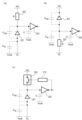
図3(a)、図3(b)及び図3(c)は、クエンチ素子202のいくつかの構成例を説明する回路図である。図3(a)は、光電変換部201のカソード側にクエンチ素子202として抵抗値Rを有する抵抗素子が配される構成例を示す回路図である。光電変換部201、クエンチ素子202及び波形整形部203の接続関係は図2と同様であるため説明を省略する。また、図3(a)には、光電変換部201のPN接合容量CPD、光電変換部201のウエル容量Cw及び配線及び拡散層の寄生容量Cが図示されている。図3(a)に示されているVsubは基板電位を示している。
3(a), FIG. 3(b), and FIG. 3(c) are circuit diagrams illustrating some configuration examples of the quench
光電変換部201のPN接合容量CPDは、アバランシェ増倍を生じさせるために強電界が誘起される検出領域の容量である。そのため、PN接合容量CPDは、検出領域の面積に比例する。
The PN junction capacitance CPD of the
図3(a)の構成において、アバランシェ電流により波形整形部203の入力電位が変化してから、クエンチ素子202による電圧降下によって光電変換部201のバイアスが初期状態に復帰するまでには一定の時間が必要である。光電変換素子101が一度電荷を検出してから、次に電荷を検出することが可能な状態に戻るまでの時間は、デッドタイム(Dead time)と呼ばれる。このデッドタイムが短いほど、単位時間にカウントできる電荷の個数が増加し、光検出装置1010のダイナミックレンジが大きくなる。
In the configuration of FIG. 3A, it takes a certain amount of time after the input potential of the
図3(a)の構成例における光電変換素子101のデッドタイムτdは、以下の式(1)により求められる。
![]()
![]()
図3(b)は、光電変換部201のアノード側にクエンチ素子202として抵抗値Rを有する抵抗素子が配される構成例を示す回路図である。本例においては、光電変換部201のカソードには電位VHが供給される。光電変換部201のアノードはクエンチ素子202の一端に接続されている。クエンチ素子202の他端には、電位VHよりも低い電位VLが供給される。
FIG. 3B is a circuit diagram showing a configuration example in which a resistance element having a resistance value R is arranged as the quench
図3(b)の構成例における光電変換素子101のデッドタイムτdは、以下の式(2)により求められる。
![]()
![]()
図3(c)は、光電変換部201のカソード側にクエンチ素子202としてスイッチが配される構成例を示す回路図である。クエンチ素子202は、クエンチ素子制御部210によりオン状態又はオフ状態に制御されるように構成されている。クエンチ素子制御部210は、波形整形部203から出力されたパルスを遅延させて出力する。これにより、クエンチ素子制御部210は、アバランシェ増倍が発生した直後にクエンチ素子202をオフ状態に制御するように構成されている。本構成例によれば、クエンチ動作が能動的に行われることにより、クエンチ素子202に受動素子を用いた場合と比べてデッドタイムを短縮することができる。
FIG. 3C is a circuit diagram showing a configuration example in which a switch is arranged as the quench
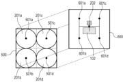
図4(a)及び図4(b)は、本実施形態に係る光電変換素子101の構成例を示す図である。図4(a)は、光電変換素子101及び画素信号処理部102が形成されている半導体基板に対して垂直な方向からの平面視による模式図である。図4(b)は、光電変換素子101の回路図である。
FIGS. 4A and 4B are diagrams showing an example of the configuration of the
図4(a)に示されるように、1つの画素100には4つの光電変換部201a、201b、201c、201dが設けられている。4つの光電変換部201a、201b、201c、201dは、2行及び2列をなす行列状に配されている。画素信号処理部102は、4つの光電変換部201a、201b、201c、201dの中心付近に配されている。クエンチ素子202は2つの光電変換部201a、201cの間に配されている。
As shown in FIG. 4A, one
このように、本実施形態では、4つの光電変換部201a、201b、201c、201dと、画素信号処理部102と、クエンチ素子202とが同一の半導体基板の同一の面に形成されている。これにより、これらを別の基板に形成する場合と比較して製造コストを低減させることができる。この面積低減効果は、クエンチ素子202が抵抗素子等の受動素子である場合よりも、図3(c)のような能動クエンチ回路である場合の方が大きい。一般的に、能動クエンチ回路の方が受動素子よりも素子面積が大きいためである。
In this manner, in this embodiment, the four
図4(b)に示されるように、1つのクエンチ素子202が、4つの光電変換部201a、201b、201c、201dに対して直列に接続されている。クエンチ素子202と光電変換部201a、201b、201c、201dとが接続されるノード221において、4つの光電変換部201a、201b、201c、201dのカソードから延びる配線は1つに束ねられている。
As shown in FIG. 4(b), one quench
図5(a)及び図5(b)は、本実施形態の比較例に係る光電変換素子101の構成例を示す図である。図5(a)は、光電変換素子101及び画素信号処理部102が形成されている半導体基板に対して垂直な方向からの平面視による模式図である。図5(b)は、光電変換素子101の回路図である。
FIGS. 5A and 5B are diagrams showing a configuration example of a
図5(a)及び図5(b)に示される比較例において図4(a)及び図4(b)と相違する点は、4つのクエンチ素子231a、231b、231c、231dが設けられている点である。4つのクエンチ素子231a、231b、231c、231dは、4つの光電変換部201a、201b、201c、201dにそれぞれ対応して設けられている。4つのクエンチ素子231a、231b、231c、231dは、それぞれ、4つの光電変換部201a、201b、201c、201dに対して直列に接続されている。
The comparative example shown in FIGS. 5(a) and 5(b) is different from FIGS. 4(a) and 4(b) in that four quench
図4(a)及び図4(b)に示されている本実施形態の構成では、4つの光電変換部201a、201b、201c、201dに直列接続されるクエンチ素子202が1つに共通化されている。これにより、図5(a)及び図5(b)に示される比較例において生じ得るクエンチ素子231a、231b、231c、231dの性能のばらつきに起因する出力信号の精度への影響を低下させることができる。この効果について、図6(a)、図6(b)、図7(a)、図7(b)、図8(a)及び図8(b)を参照してより詳細に説明する。
In the configuration of this embodiment shown in FIGS. 4(a) and 4(b), the quench
図6(a)及び図6(b)は、本実施形態の比較例における各ノードの電位を示すグラフである。各グラフの横軸は時間を、縦軸は電位をそれぞれ示している。なお、本明細書において、各グラフの軸の単位は任意であり、グラフ間でスケールは一致していない。図6(a)は、4つの光電変換部201a、201b、201c、201dのそれぞれに異なるタイミングで1個の光子が入射した際の、ノード232a、232b、232c、232dの電位の変化を示すグラフである。ノード232a、232b、232c、232dの各グラフは重ならないように縦方向にずらして図示されている。図6(a)は、各光電変換部に光子が入射したタイミングで、各ノードの電位が低下し、その後所定の時間(デッドタイム)が経過するとクエンチ動作により元の電位に戻ることを示している。
FIGS. 6A and 6B are graphs showing the potential of each node in a comparative example of this embodiment. The horizontal axis of each graph represents time, and the vertical axis represents potential. Note that in this specification, the units of the axes of each graph are arbitrary, and the scales of the graphs do not match. FIG. 6(a) is a graph showing changes in the potentials of
図6(b)は、図6(a)に示すタイミングで4つの光電変換部201a、201b、201c、201dに光子が入射した際の、ノード233の電位の変化を示すグラフである。4つの光電変換部201a、201b、201c、201dのそれぞれに1個ずつ光子が入射されているため、これらを加算平均した電位であるノード233の電位は4回降下している。
FIG. 6(b) is a graph showing changes in the potential of the
図6(b)の破線は、画素信号処理部102において、電位変化をカウントする際の論理判定閾値VTの電位レベルを示している。カウンタ回路209は、電位が論理判定閾値VTよりも高い状態から論理判定閾値VTをまたいで論理判定閾値VTよりも低い状態に変化した回数をカウントする。ノード233の電位が論理判定閾値VTを下回る回数は4回であるため、カウンタ回路209によりカウントされるカウント数は4である。このカウント数は入射された光子の個数の合計と一致しており、画素信号処理部102からは適切な値が出力される。
The broken line in FIG. 6B indicates the potential level of the logic determination threshold VT when counting potential changes in the pixel
しかしながら、クエンチ素子231a、231b、231c、231dのうちの、いずれか1つでも理想的な動作を行えない場合、ノード233における電位の波形は、図6(b)に示すものとは異なる波形となる。図7(a)及び図7(b)には、クエンチ素子231bの実効的な抵抗値が、他のクエンチ素子231a、231c、231dよりも大きい場合の各ノードの電位を示すグラフが示されている。図7(a)及び図7(b)において、4つの光電変換部201a、201b、201c、201dへの光子の入射タイミングは図6(a)及び図6(b)の場合と同様である。
However, if any one of the quench
図7(a)において、ノード232a、232c、232dの電位の変化は図6(a)に示されているものと同様である。しかしながら、ノード232bについては、電位が低下してから、元に戻るまでの時間が長くなっている。この理由は、クエンチ素子231bの実効的な抵抗値が大きいため回路の時定数が大きくなり、上述の式(1)又は式(2)に示されているデッドタイムτdが大きくなるためである。
In FIG. 7(a), changes in the potentials of
この場合において、ノード233の電位は、図7(b)に示されるものとなる。ノード233の電位が論理判定閾値VTをまたいで下回る回数は2回である。そのため、カウンタ回路209によりカウントされるカウント数は2である。このように、比較例では、ノード232bでの電位の低下が戻る時間が長くなっている影響により、光電変換部201c、201dに光子が入射した時刻における電位降下量はカウントされない。このように、比較例においては、カウント数が入射された光子の個数の合計と一致せず、画素信号処理部102から出力される値の精度が低下する場合がある。
In this case, the potential of the
図4(a)及び図4(b)に示されている本実施形態の構成では、4つの光電変換部201a、201b、201c、201dは、1つのクエンチ素子202に直列接続されている。この場合、クエンチ素子202が1つであるため、異なるクエンチ素子間の性能ばらつきに起因する精度劣化は生じない。この場合における各ノードの電位が図8(a)及び図8(b)に示されている。図8(a)及び図8(b)において、4つの光電変換部201a、201b、201c、201dへの光子の入射タイミングは図6(a)及び図6(b)の場合と同様である。
In the configuration of this embodiment shown in FIGS. 4A and 4B, four
図8(a)は、図4(a)のノード221における電位の変化を示すグラフである。4つの光電変換部201a、201b、201c、201dは、出力電位が配線上で加算平均された状態でクエンチ素子202に接続されている。そのため、電位が降下する回数は、光電変換部201a、201b、201c、201dに入射される光子の個数と一致する。
FIG. 8(a) is a graph showing changes in the potential at the
図8(b)は、図4(a)のノード222における電位の変化を示すグラフである。本構成では、ノード222は、ノード221と同電位であるため、図8(b)は、図8(a)と同様の波形である。そのため、ノード222の電位が論理判定閾値VTを下回る回数は4回であり、カウンタ回路209によりカウントされるカウント数は4である。このカウント数は入射された光子の個数の合計と一致しており、画素信号処理部102からは適切な値が出力される。
FIG. 8(b) is a graph showing changes in the potential at the
以上のように、本実施形態においては、4つの光電変換部201a、201b、201c、201dは1つのクエンチ素子202に直列接続されている。そのため、異なるクエンチ素子間の性能ばらつきに起因する精度劣化は生じない。したがって、本実施形態によれば、出力信号の精度が向上された光検出装置1010が提供される。
As described above, in this embodiment, the four
また、本実施形態では、4つの光電変換部201a、201b、201c、201dに対して、1つのクエンチ素子202を設ける構成であるため、光電変換部ごとにクエンチ素子を設ける構成に比べてクエンチ素子の素子数を少なくすることができる。そのため、クエンチ素子の配置に要する素子面積を低減することができ、その分の素子面積を光電変換部の面積に割り当てることにより、光検出装置1010の検出感度を向上させることができる。
Furthermore, in this embodiment, since one quench
[第2実施形態]
第1実施形態では、図4(a)に示されるように、4つの光電変換部201a、201b、201c、201dと、画素信号処理部102と、クエンチ素子202とが同一の半導体基板の同一の面に形成されている。これに対し、本実施形態では、4つの光電変換部201a、201b、201c、201dが第1の基板500に形成され、画素信号処理部102とクエンチ素子202とが第1の基板500とは異なる第2の基板600に形成される例を説明する。
[Second embodiment]
In the first embodiment, as shown in FIG. 4A, the four
図9は、本実施形態に係る画素100の構成例を示す模式図である。図9に示されるように、本実施形態の光検出装置1010は、第1の基板500と第2の基板600を有する。4つの光電変換部201a、201b、201c、201dは、第1の基板500上に形成される。画素信号処理部102及びクエンチ素子202は、第2の基板600に形成される。
FIG. 9 is a schematic diagram showing a configuration example of the
第1の基板500は、電極501a~501dを有し、第2の基板600は、電極601a~601dを有する。電極501a~501dと電極601a~601dとは、それぞれ相互に電気的に接続される。これにより、第1実施形態と同様の回路構成が実現される。
The
本実施形態においても、第1実施形態と同様に出力信号の精度が向上された光検出装置1010が提供される。更に、画素信号処理部102及びクエンチ素子202を光電変換部201a、201b、201c、201dを別の基板に形成することにより、光電変換部201a、201b、201c、201dの面積を大きくすることができる。これにより、受光面積が広くなるため、光検出装置1010の検出感度を向上させることができる。
In this embodiment as well, a
一方、本実施形態では、第1実施形態の場合と比べて、基板の枚数が増加する等の理由により製造コストが増加する。したがって、コスト低減が優先される場合には、第1実施形態の構成の方が望ましい場合もある。 On the other hand, in this embodiment, compared to the case of the first embodiment, manufacturing costs increase due to reasons such as an increase in the number of substrates. Therefore, if cost reduction is a priority, the configuration of the first embodiment may be more desirable.
[第3実施形態]
第1実施形態では、図4(a)に示されるように、4つの光電変換部201a、201b、201c、201dの面積が同一である。これに対し、本実施形態では、光電変換部201aの面積が、光電変換部201b、201c、201dよりも小さい例を説明する。
[Third embodiment]
In the first embodiment, as shown in FIG. 4(a), the four
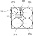
図10は、本実施形態に係る画素100の構成例を示す模式図である。本実施形態では、光電変換部201aの面積が、光電変換部201b、201c、201dよりも小さい。光電変換部201b、201c、201dのうちのいずれかが配されている領域を第1の領域、光電変換部201aが配されている領域を第2の領域700とすると、第1の領域と第2の領域700とは、行列状に配列されている。第2の領域700内には、光電変換部201aと、クエンチ素子202と、画素信号処理部102とが配置される。この構成により、第1実施形態の場合と比べて光電変換部201b、201c、201dの面積を大きくすることが可能となり、光検出装置1010の検出感度を向上させることができる。
FIG. 10 is a schematic diagram showing a configuration example of the
なお、光電変換部201aについては、第1実施形態の場合と比べて面積が小さくなり得る。しかしながら、光電変換部201a上に設けられるマイクロレンズ等の光学系の設計を最適化して、入射光を光電変換部201aの受光領域に集光させることで、面積の縮小に起因する感度低下を補償することができる。
Note that the area of the
[第4実施形態]
第1実施形態では、図4(a)に示されるように、4つの光電変換部201a、201b、201c、201dに対して1つのクエンチ素子202が接続されている。これに対し、本実施形態では、4つの光電変換部201a、201b、201c、201dに対して2つのクエンチ素子202a、202bが接続される例を説明する。
[Fourth embodiment]
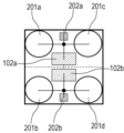
In the first embodiment, one quench
図11は、本実施形態に係る画素100の構成例を示す模式図である。本実施形態の画素100は、2つのクエンチ素子202a、202bと、2つの画素信号処理部102a、102bとを有する。2つの光電変換部201a、201cは、1つのクエンチ素子202a及び画素信号処理部102aに接続される。2つの光電変換部201b、201dは、1つのクエンチ素子202b及び画素信号処理部102bに接続される。このように、本実施形態では、1つのクエンチ素子と、2つの光電変換部と、1つの画素信号処理部とが組となって1つの領域に配されており、この領域が半導体基板上に複数個配列されている。
FIG. 11 is a schematic diagram showing a configuration example of the
第1実施形態では、4つの光電変換部で得られた信号を加算して検出する構成であるのに対し、本実施形態では、2つの光電変換部で得られた信号を加算して検出する構成である。これにより、本実施形態では1つの画素100から2つの信号が得られる。そのため、第1実施形態の構成に比べ、光検出装置1010により取得される画像の空間分解能が向上する。
In the first embodiment, the configuration is such that the signals obtained by four photoelectric conversion units are added together for detection, whereas in this embodiment, the signals obtained by two photoelectric conversion units are added together for detection. It is the composition. As a result, two signals are obtained from one
なお、本実施形態の光電変換部201a、201b、201c、201dは、第1実施形態のそれらと比べて面積が小さくなり得る。しかしながら、第3実施形態と同様に、マイクロレンズ等の光学系の設計を最適化して、入射光を受光領域に集光させることで、面積の縮小に起因する感度低下を補償することができる。
Note that the
[第5実施形態]
第1実施形態では、図4(a)に示されるように、2つの光電変換部201a、201cの間に1つのクエンチ素子202が配置されている。これに対し、本実施形態では、8つの光電変換部201a~201hの各々が配されている第1の領域の中央の第2の領域701に1つのクエンチ素子202が配置される例を説明する。
[Fifth embodiment]
In the first embodiment, as shown in FIG. 4(a), one quench
図12は、本実施形態に係る画素100の構成例を示す模式図である。本実施形態の画素100は、8つの光電変換部201a~201hを有する。8つの光電変換部201a~201hの各々が配されている第1の領域の中央は、光電変換部が設けられていない第2の領域701である。第1の領域及び第2の領域701は、3行及び3列をなす行列状に配されている。第2の領域701には、画素信号処理部102及びクエンチ素子202が配置されている。
FIG. 12 is a schematic diagram showing a configuration example of the
第1実施形態の構成において、光電変換部の面積が小さい場合には、画素100内に光電変換部、クエンチ素子202及び画素信号処理部102を1つの領域に収めて行列状に配列することが困難になる。本実施形態では、第2の領域701内に、光電変換部を配置せずに、クエンチ素子202と画素信号処理部102のみを配置する構成とすることで、レイアウト設計が容易になる。
In the configuration of the first embodiment, when the area of the photoelectric conversion section is small, the photoelectric conversion section, the quench
[第6実施形態]
図13(a)、図13(b)及び図13(c)は、光電変換部2070の断面構造を模式的に示す図である。図13(a)、図13(b)及び図13(c)に示すように、光電変換部2070は、半導体基板に形成されたN型半導体領域2001、P型半導体領域2002、N型半導体領域2003、及びN型半導体領域2012を含む。N型半導体領域2001とP型半導体領域2002とは、光を信号電荷に変換して蓄積するPD(フォトダイオード)を構成する。P型半導体領域2002と、N型半導体領域2003と、N型半導体領域2012と、はAD(アバランシェダイオード)を構成する。後述するが、光電変換部2070の動作期間は、信号電荷がPDに蓄積される蓄積期間と、PDに蓄積した信号電荷がADに転送される読出期間とに大別される。読出期間のうちの少なくとも一部の期間には、転送される信号電荷によりADにおいてアバランシェ増倍が生じる。
[Sixth embodiment]
13(a), FIG. 13(b), and FIG. 13(c) are diagrams schematically showing the cross-sectional structure of the
光電変換部2070は、N型半導体領域2001の下方に形成されるP型半導体領域2009と、N型半導体領域2001、2012の側方に形成されるP型半導体領域2010、2011とを更に含む。P型半導体領域2010、2011は、隣接する光電変換部2070同士を分離する。
これらの半導体領域の断面構造における配置は、図13(a)等に示される通りである。特に、N型半導体領域2001は、P型半導体領域2002、2009、2010によって囲まれている。また、N型半導体領域2001とN型半導体領域2003との間には、少なくとも部分的に、P型半導体領域2002が配される。N型半導体領域2012は、N型半導体領域2003よりも低い不純物濃度を有し、かつ、P型半導体領域2002とN型半導体領域2003との間に配されている。N型半導体領域2012の少なくとも一部はアバランシェ増倍部を形成する。なお、図13(a)、図13(b)及び図13(c)において、入射光は図中の上側から入射されるものとする。
The arrangement of these semiconductor regions in the cross-sectional structure is as shown in FIG. 13(a) and the like. In particular, N-
N型半導体領域2003には、電位制御部2005が接続されている。電位制御部2005は、N型半導体領域2003に電位Vnを印加している。P型半導体領域2011には、電位制御部2006が接続されている。電位制御部2006は、P型半導体領域2011に電位Vpを印加している。電位Vpは、P型半導体領域2011を介して、P型半導体領域2002、2009、2010にも供給され得る。図13(a)に示す状態では、N型半導体領域2001は電気的にフローティングとなっている。
A
半導体基板の内部のポテンシャル分布は、上述の各半導体領域の配置、各半導体領域の不純物濃度分布、電位制御部2005及び電位制御部2006に印加される電位によって決定される。したがって、電位制御部2005及び電位制御部2006に印加される電位を制御することにより、上述の蓄積期間状態と読出期間状態とを切り替えることができる。また、信号電荷転送時においてアバランシェ増倍を生じさせる等の所定のポテンシャルの状態を実現するために、上述の各半導体領域の配置、及び、各半導体領域の不純物濃度分布が、光検出装置の設計時に調整され得る。
The potential distribution inside the semiconductor substrate is determined by the arrangement of each semiconductor region described above, the impurity concentration distribution of each semiconductor region, and the potentials applied to the
図13(a)、図13(b)、図13(c)は、N型半導体領域2003に印加する電位Vnの値をVn0、Vn1、Vn2と変化させた例を示している。また、図14(a)、図14(b)、図14(c)は、図13(a)、図13(b)、図13(c)のそれぞれに対応するA-A’におけるポテンシャルを示す図である。この3つの例では、N型半導体領域2001とN型半導体領域2003との間に生じるポテンシャル障壁の高さが互いに異なる。これにより、N型半導体領域2001に信号電荷を蓄積する期間と、N型半導体領域2001からN型半導体領域2003に信号電荷を読み出す期間とが制御される。説明の単純化のために、図13(a)、図13(b)、図13(c)では、P型半導体領域2002に固定の電位Vpが印加されているものとしているが、P型半導体領域2002に印加される電位が互いに異なっていてもよい。なお、図13(a)、図13(b)及び図13(c)の破線は、空乏層の端部を示している。
13(a), FIG. 13(b), and FIG. 13(c) show examples in which the value of the potential Vn applied to the N-
図13(a)は、N型半導体領域2001に信号電荷が蓄積される状態の光電変換部2070を示す図であり、図14(a)は図13(a)のA-A’におけるポテンシャルを示す図である。電位制御部2005に印加される電位Vn0は、電位制御部2006に印加される電位Vpよりも高い。すなわち、PN接合には逆バイアスが印加されており、PN接合面の付近には空乏層が広がっている。図13(a)に示されるように、P型半導体領域2002の一部には中性領域が存在している。P型半導体領域2002の中性領域には、P型半導体領域の多数キャリアであるホールが多数存在している。そのため、P型半導体領域2002の中性領域の電位は、電位制御部2006の電位Vpとほぼ同じである。なお、P型半導体領域2011、2010、2009にも、それぞれ中性領域が存在しているものとする。
FIG. 13(a) is a diagram showing the
暗状態、すなわち信号電荷が無い場合において、図13(a)の状態では、N型半導体領域2001の全体に空乏層が広がっている。このとき、P型半導体領域2002の中性領域(及び周囲にある他のP型半導体領域の中性領域)とN型半導体領域2001との間には、いわゆる「空乏化電圧」と呼ばれる逆バイアス電圧が少なくとも生じている。換言すると、N型半導体領域2001に存在する信号電荷(電子)に対しては、PN接合間のビルトインポテンシャルに空乏化電圧を加えた電圧に相当するポテンシャル障壁がN型半導体領域2001の周囲に生じている。したがって、A-A’に沿ったポテンシャル分布において、図14(a)に示すように、N型半導体領域2001とN型半導体領域2003との間に、N型半導体領域2001の電子に対するポテンシャル障壁が生じている。なお上述のPDの空乏化電圧は、典型的には、CMOSセンサ、CCDセンサ等のイメージセンサにおけるPDの空乏化電圧と同レベルであり、すなわち1V~2V程度である。
In the dark state, that is, when there is no signal charge, the depletion layer spreads over the entire N-
図13(a)では、N型半導体領域2003に印加される電位Vn0は、電位制御部2006に印加される電位Vpよりも高い。したがって、P型半導体領域2002、2011と、N型半導体領域2003、2012との間のPN接合には、電位Vn0と電位Vpとの差分に相当する逆バイアスが印加される。また、当該逆バイアスに応じた空乏層が、P型半導体領域2002及びP型半導体領域2011に広がっている。この図13(a)の状態において、P型半導体領域2002とN型半導体領域2003、2012とで形成されるADのPN接合では基本的にはアバランシェ増倍が起こらないように電位Vn0が設定される。また、光入射により発生した信号電荷はN型半導体領域2001に蓄積される。
In FIG. 13A, the potential Vn0 applied to the N-
図13(b)は、N型半導体領域2003に印加される電位Vnが、Vn0から、Vn0よりも高いVn1に変化した状態を示す図である。Vn1はVn0より高い電位であり、一方で、Vpは固定である。そのため、P型半導体領域2002、2011と、N型半導体領域2003、2012との間のPN接合には、図13(a)の場合と比べて大きな逆バイアスが印加される。また、それに応じて、P型半導体領域2002の空乏層が図13(a)の場合に比べて広がる。その結果、電位VnがVn1の時に、N型半導体領域2001の周囲のP型半導体領域2002の空乏層と、N型半導体領域2003の周囲のP型半導体領域2002の空乏層とがつながる。換言すると、N型半導体領域2001からN型半導体領域2003まで、空乏層が連続的に延びた状態となる。
FIG. 13(b) is a diagram showing a state in which the potential Vn applied to the N-
P型半導体領域2002のうち、空乏化している部分のポテンシャルは、P型半導体領域2002の中性領域のポテンシャル(ほぼVpと同じ)よりも低い。これは、N型半導体領域2003に印加される電位Vnの影響を受けるためである。したがって、図13(b)のA-A’に沿ったポテンシャル分布においては、図14(b)が示す通り、N型半導体領域2001とN型半導体領域2003との間のポテンシャル障壁の高さが、図13(a)の場合に比べて低くなる。
The potential of the depleted portion of the P-
このとき、N型半導体領域2001の周囲のほとんどをP型半導体領域2002、2009、2010の中性領域が取り囲んでいる。そして、電位制御部2006の電位Vpは固定である。そのため、N型半導体領域2001の中心のポテンシャルはほとんど変化しない。したがって、上述の通り、N型半導体領域2001に対するポテンシャル障壁の高さを、局所的に下げることができる。
At this time, most of the periphery of the N-
図13(b)において、N型半導体領域2001に信号電荷が蓄積されている場合は、ポテンシャル障壁を超えて信号電荷がN型半導体領域2003に転送され始める。このとき、N型半導体領域2003とP型半導体領域2002との間には、アバランシェ増倍が起こる程度の逆バイアス電圧が生じている状態となっていることが好ましい。
In FIG. 13B, when signal charges are accumulated in the N-
連続的な空乏層が形成された後、N型半導体領域2003に印加される電位VnがVn1からVn1よりも高い電位Vn2へ変化する。これに応じて、ポテンシャル障壁が徐々に低下する。また、電位Vnの変化に応じて、P型半導体領域2002に生じる空乏層の幅も変化する。
After a continuous depletion layer is formed, the potential Vn applied to the N-
図13(c)は、N型半導体領域2001とN型半導体領域2003との間のポテンシャル障壁がほぼなくなった状態を示す図である。また、図14(c)は、図13(c)のA-A’のポテンシャルを示す図である。このとき、N型半導体領域2003には電位Vn2が印加されている。図14(c)の状態では、N型半導体領域2001に蓄積された信号電荷がN型半導体領域2003にすべて転送される。すなわち、完全空乏化転送が可能となる。
FIG. 13(c) is a diagram showing a state in which the potential barrier between the N-
このような完全空乏化転送に必要な電圧は、P型半導体領域2002の不純物濃度が低いほど低くなり、逆に、P型半導体領域2002の不純物濃度が高いほど高くなる。前述のように信号電荷が転送されている期間の少なくとも一部で、P型半導体領域2002とN型半導体領域2003との間にアバランシェ増倍が生じる逆バイアスが生じるように、P型半導体領域2002やN型半導体領域2012の不純物濃度が設定される。
The voltage required for such complete depletion transfer becomes lower as the impurity concentration of the P-
なお、暗状態において、電位Vnが図13(b)の状態から図13(c)の状態に変化するときに、N型半導体領域2001のポテンシャルが多少変化することが考えられる。しかしながら、N型半導体領域2001よりもP型半導体領域2002の方が、電位Vnの供給されるN型半導体領域2003に近いため、P型半導体領域2002の方が電位Vnの変化の影響をより強く受ける。したがって、P型半導体領域2002の空乏化した部分のポテンシャルの方がN型半導体領域2001のポテンシャルよりも変化しやすい。結果として、N型半導体領域2001とN型半導体領域2003との間のポテンシャルバリアを無くすことができる。
Note that in the dark state, when the potential Vn changes from the state shown in FIG. 13(b) to the state shown in FIG. 13(c), the potential of the N-
本実施形態では、図13(c)において、P型半導体領域2009及びP型半導体領域2010には中性領域が残った状態である。この構成によれば、N型半導体領域2001の周囲の大部分に電位Vpを供給できるため、図14(b)及び図14(c)の状態において、N型半導体領域2001のポテンシャルの変化を小さく抑えることができる。したがって、電位Vnの変化量がさほど大きくなくても、電荷の完全転送が可能である。ただし、電位VnがVn0からVn2に変化する過程で、P型半導体領域2009又はP型半導体領域2010の全体が空乏化することもあり得る。
In this embodiment, in FIG. 13C, neutral regions remain in the P-
以上に説明した通り、本実施形態の光電変換部2070は、電位Vnが制御されることにより、N型半導体領域2001とN型半導体領域2003との間のポテンシャル障壁の高さを制御することができる。したがって、本実施形態の光電変換部2070を備える光検出装置は、N型半導体領域2001に信号電荷を蓄積する動作と、N型半導体領域2001からN型半導体領域2003に信号電荷を読み出す動作と、を選択的に実施することができる。
As explained above, the
ここで、図13(b)において信号電荷が転送されたときに、アバランシェ増倍が生じることが好ましいと説明した。しかしながら、電位VnがVn0からVn2に変化する間に、アバランシェ増倍が起きる大きさの逆バイアスが印加されるタイミングと、空乏層がつながるタイミング(すなわち、ポテンシャル障壁が下がり始めるタイミング)とがずれていてもよい。アバランシェ増倍が起きる大きさの逆バイアスが印加されるタイミングとP型半導体領域2002において空乏層がつながるタイミングとは、どちらが先であってもよい。N型半導体領域2001における飽和電荷量は、アバランシェ増倍によって信号検出が開始できるようなバイアス電圧が印加されるときのポテンシャル障壁で決まる。
Here, it has been explained that avalanche multiplication preferably occurs when signal charges are transferred in FIG. 13(b). However, while the potential Vn changes from Vn0 to Vn2, the timing at which a reverse bias large enough to cause avalanche multiplication is applied is different from the timing at which the depletion layer connects (that is, the timing at which the potential barrier begins to fall). It's okay. The timing at which a reverse bias large enough to cause avalanche multiplication is applied and the timing at which the depletion layer is connected in the P-
上述の構成の光電変換部2070を備える光電変換素子101の構成例を説明する。図15(a)及び図15(b)は、本実施形態に係る光電変換素子101の構成例を示す図である。図15(a)及び図15(b)において、図4(a)及び図4(b)との差異点は、光電変換部201a、201b、201c、201dのそれぞれに対して、スイッチ素子241a、241b、241c、241dが追加されている点である。ここで、光電変換部201a、201b、201c、201dは、いずれも上述の光電変換部2070と同様の構成を有しているものとする。光電変換部201aは、スイッチ素子241aを間に介してクエンチ素子202との接続ノードであるノード221に接続されている。光電変換部201bは、スイッチ素子241bを間に介してノード221に接続されている。光電変換部201cは、スイッチ素子241cを間に介してノード221に接続されている。光電変換部201dは、スイッチ素子241dを間に介してノード221に接続されている。
A configuration example of the
図15(b)に示すように、初期状態において、スイッチ素子241a、241b、241c、241dは、全てオン状態であり、電位VH0が光電変換部201a、201b、201c、201dに供給されている。その後、例えば、スイッチ素子241aだけをオン状態とし、その他のスイッチ素子241b、241c、241dはオフ状態にすると、光電変換部201aだけに電位VH0が供給される状態となる。
As shown in FIG. 15(b), in the initial state, the
図16に示すタイミングチャートを用いて、光電変換素子101の駆動方法を説明する。図中の「カソード電位」は、電位制御部2005に印加される電位を示しており、図中の「241a」、「241b」、「241c」、「241d」は、対応するスイッチ素子のオン状態又はオフ状態を示している。
A method for driving the
上述の初期状態の後、スイッチ素子241a、241b、241c、241dはオフ状態になり、光電変換部201a、201b、201c、201dは電荷が蓄積される蓄積状態となる。時刻t1において、スイッチ素子241aのみがオン状態になる。この時点において、他のスイッチ素子241b、241c、241dはオフ状態のままに維持されている。時刻t2以前の時点において、光電変換部201aのカソード電位はVH0である。このとき、光電変換部201aには、アバランシェ増倍が起きるのに必要なバイアス電圧は印加されておらず、光電変換部201aは、ポテンシャル障壁が下がり始める前の状態である。したがって、光電変換部201aに蓄積された電荷は電位制御部2005から読み出されない。言い換えると、時刻t2以前の期間は蓄積期間251aである。このときの図13(a)のA-A’のポテンシャルが図14(a)である。図14(a)に示されるように、N型半導体領域2001に蓄積された電荷はP型半導体領域2002のポテンシャル障壁により、N型半導体領域2003に到達していない。
After the above-mentioned initial state, the
時刻t2において、光電変換部201aのカソード電位がVH0から遷移を開始する。カソード電位がVH1になった時点から、光電変換部201aには、アバランシェ増倍が起きるのに必要なバイアスが印加され始める。これにより、ポテンシャル障壁が下がり、蓄積電荷が徐々に読み出され始める。このときの図13(b)のA-A’のポテンシャルが図14(b)である。図14(b)に示されるように、P型半導体領域2002のポテンシャル障壁が下がることにより、N型半導体領域2001に蓄積された電荷のうちの一部がN型半導体領域2003に到達する。
At time t2, the cathode potential of the
時刻t2から時刻t3の期間にわたって光電変換部201aのカソード電位がVH0からVH2に徐々に遷移する。時刻t3付近において、光電変換部201aにはアバランシェ増倍が起きるのに十分なバイアスが印加され、蓄積された信号電荷はすべて転送され完全空乏化転送が実現する。このときの図13(c)のA-A’のポテンシャルが図14(c)である。図14(c)に示されるように、P型半導体領域2002のポテンシャル障壁が下がることにより、N型半導体領域2001に蓄積された電荷のすべてが、N型半導体領域2003に到達する。このようにして、光電変換部201aに蓄積された電荷が読み出される。言い換えると、時刻t2から時刻t3までの期間は読出期間252aである。
Over the period from time t2 to time t3, the cathode potential of the
その後、時刻t3において光電変換部201aのカソード電位がVH2からVH0に遷移する。これにより、光電変換部201aには、アバランシェ増倍が起きるのに必要なバイアスが印加されない状態となり、ポテンシャル障壁が時刻t2以前と同じ状態に戻る。言い換えると、時刻t3以降の期間は蓄積期間251aである。なお、読出期間252aの後には、光電変換部201aから転送された電荷のカウント数がリセットされる。
Thereafter, at time t3, the cathode potential of the
上述の光電変換部201aからの読み出しと同様の処理が光電変換部201b、201c、201dに対しても、順次行われる。これにより、光電変換部201a、201b、201c、201dに蓄積された電荷が、順次読み出される。
Processing similar to the above-described reading from the
上述の第1実施形態では、出力された信号が4つの光電変換部201a、201b、201c、201dのうちのいずれで発生した電荷によるものであるかを区別できない回路構成となっている。これに対し、本実施形態では、光電変換部201a、201b、201c、201dのそれぞれに対して個別に読み出しを行うよう制御することが可能である。したがって、本実施形態によれば、出力された信号が4つの光電変換部201a、201b、201c、201dのうちのいずれで発生した電荷によるものであるかを区別することが可能な光検出装置1010が提供される。なお、本実施形態において、信号電荷は正孔であってもよく、その場合、各半導体領域のN型とP型は反対になる。
In the first embodiment described above, the circuit configuration is such that it is not possible to distinguish which of the four
[第7実施形態]
本実施形態では、図17を参照しつつ、第1乃至第6実施形態の光検出装置1010を用いた光検出システムの一例を説明する。本実施形態の光検出システムは、不可視光である波長帯の光を検出する不可視光検出システムであり、PET(Positron Emission Tomography)等の医療診断システムに用いられる。なお、本実施形態の画素100は、図2のカウンタ回路209に代えてTDC204及びメモリ205を有する。
[Seventh embodiment]
In this embodiment, an example of a photodetection system using the
図17は、不可視光検出システムのブロック図である。不可視光検出システムは、複数の光検出装置1010A、1010B、波長変換部1201及びデータ処理部1207を有している。複数の光検出装置1010A、1010Bの各々は、カウンタ回路209に代えてTDC204及びメモリ205を有している点を除いては、第1乃至第6実施形態の光検出装置1010と同様である。
FIG. 17 is a block diagram of an invisible light detection system. The invisible light detection system includes a plurality of
照射物1200は、不可視光である波長帯(第1波長帯)の光を照射する。波長変換部1201は、照射物1200から照射された不可視光を受光し、可視光である波長帯(第2波長帯)の光を照射する。波長変換部1201から照射された可視光は光電変換部201に入射される。光電変換部201は、入射光を光電変換して電気信号に変換する。この電気信号は、クエンチ素子202、波形整形部203、TDC204を介して、デジタル信号としてメモリ205に保持される。複数の光検出装置1010A、1010Bは、1つの装置として構成されていてもよく、複数の装置として構成されていてもよい。
The
複数の光検出装置1010A、1010Bのメモリ205に保持された複数のデジタル信号は、データ処理部1207により読み出され、信号処理が行われる。データ処理部1207は、複数のデジタル信号から得られた複数の画像の合成処理を行う信号処理手段として機能する。
A plurality of digital signals held in the
次に、不可視光検出システムの具体的な例としてPET等の医療診断システムの構成について説明する。照射物1200である被験者は、生体内からガンマ線等の放射線対を放出する。波長変換部1201は、シンチレータを含み、シンチレータは、被験者から放出された放射線対が入射すると可視光を照射する。
Next, the configuration of a medical diagnostic system such as PET will be described as a specific example of an invisible light detection system. The subject, which is the
シンチレータから照射された可視光は、光検出装置1010A、1010Bに入射し、入射光に基づくデジタル信号がメモリ205に保持される。これにより、光検出装置1010A、1010Bは、被験者から放出された放射線対のそれぞれの到達時間を検出することができる。
The visible light emitted from the scintillator enters the
複数の光検出装置1010A、1010Bのメモリ205に保持された複数のデジタル信号は、データ処理部1207により読み出され、信号処理が行われる。データ処理部1207は、複数のデジタル信号から得られた複数の画像を用いて画像再構成等の合成処理を行い、被験者の生体内の画像を生成する。
A plurality of digital signals held in the
本実施形態によれば、検出性能が向上された光検出装置1010A、1010Bを用いることにより、より高精度な不可視光検出システム、医療診断システム等の光検出システムを提供することができる。
According to this embodiment, by using the
[第8実施形態]
本実施形態では、図18及び図19を参照しつつ、第1乃至第6実施形態の光検出装置1010を用いた光検出システムの他の一例を説明する。
[Eighth embodiment]
In this embodiment, another example of a photodetection system using the
まず、図18を参照して光検出システムの一例である距離検出システムについて説明する。なお、本実施形態の画素100は、図2のカウンタ回路209に代えてTDC204及びメモリ205を有する。
First, a distance detection system, which is an example of a light detection system, will be described with reference to FIG. Note that the
図18は、距離検出システムのブロック図である。距離検出システムは、光源制御部1301、発光部1302、光学部材1303、光検出装置1010及び距離算出部1309を有している。
FIG. 18 is a block diagram of the distance detection system. The distance detection system includes a light
光源制御部1301は発光部1302の駆動を制御する。発光部1302は、光源制御部1301からの信号に応じて、撮影方向に対して短パルス(列)の光を照射する発光装置である。
A light
発光部1302から照射された光は、被写体1304において反射される。反射光は、レンズなどの光学部材1303を通して、光検出装置1010の光電変換部201で受光される。光電変換部201は、入射光に基づく信号を出力し、当該信号は、波形整形部203を介してTDC204に入力される。
Light emitted from the
TDC204は、光源制御部1301から発光部1302からの光照射のタイミングを示す信号を取得する。TDC204は、光源制御部1301から取得した信号と、波形整形部203から入力された信号とを比較する。これにより、TDC204は、発光部1302がパルス光を発光してから被写体1304で反射された反射光を受光するまでの時間をデジタル信号として出力する。TDC204から出力されたデジタル信号は、メモリ205に保持される。この処理は複数回繰り返し行われ、メモリ205が複数回分のデジタル信号を保持することができる。
The
距離算出部1309は、メモリ205に保持された複数のデジタル信号に基づいて、光検出装置1010から被写体1304までの距離を算出する。この距離検出システムは例えば、車載用の距離検出装置に適用することができる。なお、距離算出部1309で行われる処理はデジタル信号の処理であることから、より一般的に信号処理手段と呼ばれることもある。
The
次に、図19(A)及び図19(B)を参照して、光検出装置1010を車載カメラとして用いた光検出システムについて説明する。図19(A)及び図19(B)は、本実施形態による光検出システム1000及び移動体の構成を示す図である。
Next, a light detection system using the
図19(A)は、車載カメラに関する光検出システム1000の一例を示したブロック図である。光検出システム1000は、第1実施形態に係る光検出装置1010を有する。光検出システム1000は、光検出装置1010により取得された複数のデジタル信号に対し、画像処理を行う画像処理部1030を有する。更に、光検出システム1000は、画像処理部1030により取得された複数の画像データから視差(視差画像の位相差)の算出を行う視差算出部1040を有する。
FIG. 19(A) is a block diagram showing an example of a
また、光検出システム1000は、算出された視差に基づいて対象物までの距離を算出する距離計測部1050と、算出された距離に基づいて衝突可能性があるか否かを判定する衝突判定部1060と、を有する。ここで、視差算出部1040及び距離計測部1050は、対象物までの距離情報を取得する距離情報取得手段の一例である。すなわち、距離情報とは、視差、デフォーカス量、対象物までの距離等に関する情報である。
The
衝突判定部1060はこれらの距離情報のいずれかを用いて、衝突可能性を判定してもよい。距離情報取得手段は、専用に設計されたハードウェアによって実現されてもよいし、ソフトウェアモジュールによって実現されてもよいし、これらの組合せによって実現されてもよい。また、FPGA(Field Programmable Gate Array)、ASIC(Application Specific Integrated Circuit)等によって実現されてもよい。更に、これらの組合せによって実現されてもよい。
光検出システム1000は車両情報取得装置1310と接続されており、車速、ヨーレート、舵角などの車両情報を取得することができる。また、光検出システム1000は、衝突判定部1060での判定結果に基づいて、車両に対して制動力を発生させる制御信号を出力する制御装置である制御ECU1410と接続されている。
The
また、光検出システム1000は、衝突判定部1060での判定結果に基づいて、ドライバーへ警報を発する警報装置1420とも接続されている。例えば、衝突判定部1060の判定結果として衝突可能性が高い場合、制御ECU1410はブレーキをかける、アクセルを戻す、エンジン出力を抑制するなどして衝突を回避、被害を軽減する車両制御を行う。警報装置1420は音等の警報を鳴らす、カーナビゲーションシステムなどの画面に警報情報を表示する、シートベルトやステアリングに振動を与えるなどしてユーザに警告を行う。
The
本実施形態では、車両の周囲、例えば前方又は後方を光検出システム1000で撮像する。図19(B)に、車両前方(撮像範囲1510)を撮像する場合の光検出システム1000を示した。車両情報取得装置1310は、所定の動作を行うように光検出システム1000又は光検出装置1010に指示を送る。このような構成により、測距の精度をより向上させることができる。
In this embodiment, the
上述の例では他の車両と衝突しない制御を説明したが、光検出システム1000は、他の車両に追従して自動運転する制御や、車線からはみ出さないように自動運転する制御などにも適用可能である。更に、光検出システム1000は、車両に限らず、例えば、船舶、航空機あるいは産業用ロボットなどの移動体(移動装置)に適用することができる。加えて、移動体に限らず、高度道路交通システム(ITS)等、広く物体認識を利用する機器に適用することができる。
In the above example, control to avoid collisions with other vehicles was explained, but the
本実施形態によれば、検出性能が向上された光検出装置1010を用いることにより、より高性能な光検出システム及び移動体を提供することができる。
According to this embodiment, by using the
[変形実施形態]
本発明は、上述の実施形態に限らず種々の変形が可能である。例えば、いずれかの実施形態の一部の構成を他の実施形態に追加した例や、他の実施形態の一部の構成と置換した例も、本発明の実施形態である。
[Modified embodiment]
The present invention is not limited to the above-described embodiments, and various modifications are possible. For example, an example in which a part of the configuration of one embodiment is added to another embodiment, or an example in which a part of the configuration in another embodiment is replaced is also an embodiment of the present invention.
また、第7及び第8実施形態に示したシステムは、本発明の光検出装置を適用しうるシステムの構成例を示したものであり、本発明の光検出装置を適用可能なシステムは17乃至図19に示した構成に限定されるものではない。 Further, the systems shown in the seventh and eighth embodiments are examples of system configurations to which the photodetection device of the present invention can be applied, and the systems to which the photodetection device of the present invention can be applied are 17 to 17. The configuration is not limited to that shown in FIG. 19.
本発明は、上述の実施形態の1以上の機能を実現するプログラムを、ネットワーク又は記憶媒体を介してシステム又は装置に供給し、そのシステム又は装置のコンピュータにおける1つ以上のプロセッサがプログラムを読み出し実行する処理でも実現可能である。また、1以上の機能を実現する回路(例えば、ASIC)によっても実現可能である。 The present invention provides a system or device with a program that implements one or more functions of the embodiments described above via a network or a storage medium, and one or more processors in a computer of the system or device reads and executes the program. This can also be achieved by processing. It can also be realized by a circuit (for example, an ASIC) that realizes one or more functions.
なお、上述の実施形態は、いずれも本発明を実施するにあたっての具体化の例を示したものに過ぎず、これらによって本発明の技術的範囲が限定的に解釈されてはならないものである。すなわち、本発明はその技術思想、又はその主要な特徴から逸脱することなく、様々な形で実施することができる。 Note that the above-described embodiments are merely examples of implementation of the present invention, and the technical scope of the present invention should not be interpreted to be limited by these embodiments. That is, the present invention can be implemented in various forms without departing from its technical idea or main features.
102 画素信号処理部
201 光電変換部
202 クエンチ素子
1010 光検出装置
102 Pixel
Claims (12)
前記複数のアバランシェダイオードにおけるアバランシェ増倍を抑制するクエンチ素子と、
前記複数のアバランシェダイオードのそれぞれから出力される信号を加算して得られた信号を処理する画素信号処理部と、
前記複数のアバランシェダイオードの各々に対応する複数のスイッチ素子と、
を有し、
1つの前記クエンチ素子が、前記複数のアバランシェダイオードに対して直列に接続されており、
前記複数のアバランシェダイオード及び前記クエンチ素子は、同一の基板に形成されており、
前記クエンチ素子は、前記基板に垂直な方向からの平面視において、前記複数のアバランシェダイオードのうちの2つのアバランシェダイオードの間に配されており、
前記複数のスイッチ素子の各々は、対応するアバランシェダイオードと前記クエンチ素子との間に接続されており、
前記複数のスイッチ素子が互いに異なるタイミングでオン状態になることにより、前記複数のアバランシェダイオードは、互いに異なるタイミングで前記画素信号処理部に信号を出力する
ことを特徴とする光検出装置。 multiple avalanche diodes;
a quench element that suppresses avalanche multiplication in the plurality of avalanche diodes;
a pixel signal processing unit that processes a signal obtained by adding signals output from each of the plurality of avalanche diodes;
a plurality of switch elements corresponding to each of the plurality of avalanche diodes;
has
one of the quench elements is connected in series with the plurality of avalanche diodes,
The plurality of avalanche diodes and the quench element are formed on the same substrate,
The quench element is arranged between two avalanche diodes of the plurality of avalanche diodes in a plan view from a direction perpendicular to the substrate ,
Each of the plurality of switch elements is connected between a corresponding avalanche diode and the quench element,
By turning on the plurality of switch elements at mutually different timings, the plurality of avalanche diodes output signals to the pixel signal processing section at mutually different timings.
A photodetection device characterized by:
ことを特徴とする請求項1に記載の光検出装置。 A plurality of regions including one quench element and two avalanche diodes connected in series to the one quench element are arranged on the substrate. The photodetection device described in .
前記複数のアバランシェダイオードにおけるアバランシェ増倍を抑制するクエンチ素子と、
前記複数のアバランシェダイオードのそれぞれから出力される信号を加算して得られた信号を処理する画素信号処理部と、
前記複数のアバランシェダイオードの各々に対応する複数のスイッチ素子と、
を有し、
1つの前記クエンチ素子が、前記複数のアバランシェダイオードに対して直列に接続されており、
前記複数のアバランシェダイオード及び前記クエンチ素子は、同一の基板に形成されており、
前記複数のアバランシェダイオードのうちの1つを含む第1の領域と、前記クエンチ素子を含む第2の領域とが、前記基板に複数の行及び複数の列をなす行列状に配列されており、
前記複数のスイッチ素子の各々は、対応するアバランシェダイオードと前記クエンチ素子との間に接続されており、
前記複数のスイッチ素子が互いに異なるタイミングでオン状態になることにより、前記複数のアバランシェダイオードは、互いに異なるタイミングで前記画素信号処理部に信号を出力する
ことを特徴とする光検出装置。 multiple avalanche diodes;
a quench element that suppresses avalanche multiplication in the plurality of avalanche diodes;
a pixel signal processing unit that processes a signal obtained by adding signals output from each of the plurality of avalanche diodes;
a plurality of switch elements corresponding to each of the plurality of avalanche diodes;
has
one of the quench elements is connected in series with the plurality of avalanche diodes,
The plurality of avalanche diodes and the quench element are formed on the same substrate,
A first region including one of the plurality of avalanche diodes and a second region including the quench element are arranged in a matrix with a plurality of rows and a plurality of columns on the substrate,
Each of the plurality of switch elements is connected between a corresponding avalanche diode and the quench element,
By turning on the plurality of switch elements at mutually different timings, the plurality of avalanche diodes output signals to the pixel signal processing section at mutually different timings.
A photodetection device characterized by:
前記複数のアバランシェダイオードにおけるアバランシェ増倍を抑制するクエンチ素子と、
前記複数のアバランシェダイオードのそれぞれから出力される信号を加算して得られた信号を処理する画素信号処理部と、
を有し、
1つの前記クエンチ素子が、前記複数のアバランシェダイオードに対して直列に接続されており、
前記複数のアバランシェダイオード及び前記クエンチ素子は、同一の基板に形成されており、
前記複数のアバランシェダイオードのうちの1つを含む第1の領域と、前記クエンチ素子を含む第2の領域とが、前記基板に複数の行及び複数の列をなす行列状に配列されており、
前記第2の領域は、前記第1の領域に含まれるアバランシェダイオードの面積よりも小さい面積を有するアバランシェダイオードを更に含む
ことを特徴とする光検出装置。 multiple avalanche diodes;
a quench element that suppresses avalanche multiplication in the plurality of avalanche diodes;
a pixel signal processing unit that processes a signal obtained by adding signals output from each of the plurality of avalanche diodes;
has
one of the quench elements is connected in series with the plurality of avalanche diodes,
The plurality of avalanche diodes and the quench element are formed on the same substrate,
A first region including one of the plurality of avalanche diodes and a second region including the quench element are arranged in a matrix with a plurality of rows and a plurality of columns on the substrate,
The photodetecting device, wherein the second region further includes an avalanche diode having a smaller area than an avalanche diode included in the first region.
前記複数のアバランシェダイオードにおけるアバランシェ増倍を抑制するクエンチ素子と、
前記複数のアバランシェダイオードのそれぞれから出力される信号を加算して得られた信号を処理する画素信号処理部と、
を有し、
1つの前記クエンチ素子が、前記複数のアバランシェダイオードに対して直列に接続されており、
前記複数のアバランシェダイオード及び前記クエンチ素子は、同一の基板に形成されており、
前記複数のアバランシェダイオードのうちの1つを含む第1の領域と、前記クエンチ素子を含む第2の領域とが、前記基板に複数の行及び複数の列をなす行列状に配列されており、
前記第2の領域は、アバランシェダイオードを含まない
ことを特徴とする光検出装置。 multiple avalanche diodes;
a quench element that suppresses avalanche multiplication in the plurality of avalanche diodes;
a pixel signal processing unit that processes a signal obtained by adding signals output from each of the plurality of avalanche diodes;
has
one of the quench elements is connected in series with the plurality of avalanche diodes,
The plurality of avalanche diodes and the quench element are formed on the same substrate,
A first region including one of the plurality of avalanche diodes and a second region including the quench element are arranged in a matrix with a plurality of rows and a plurality of columns on the substrate,
A photodetecting device, wherein the second region does not include an avalanche diode.
前記複数のアバランシェダイオードにおけるアバランシェ増倍を抑制するクエンチ素子と、
前記複数のアバランシェダイオードのそれぞれから出力される信号を加算して得られた信号を処理する画素信号処理部と、
前記複数のアバランシェダイオードの各々に対応する複数のスイッチ素子と、
を有し、
1つの前記クエンチ素子が、前記複数のアバランシェダイオードに対して直列に接続されており、
前記複数のアバランシェダイオードは、第1の基板に形成されており、
前記クエンチ素子は、前記第1の基板とは異なる第2の基板に形成されており、
前記複数のスイッチ素子の各々は、対応するアバランシェダイオードと前記クエンチ素子との間に接続されており、
前記複数のスイッチ素子が互いに異なるタイミングでオン状態になることにより、前記複数のアバランシェダイオードは、互いに異なるタイミングで前記画素信号処理部に信号を出力する
ことを特徴とする光検出装置。 multiple avalanche diodes;
a quench element that suppresses avalanche multiplication in the plurality of avalanche diodes;
a pixel signal processing unit that processes a signal obtained by adding signals output from each of the plurality of avalanche diodes;
a plurality of switch elements corresponding to each of the plurality of avalanche diodes;
has
one of the quench elements is connected in series with the plurality of avalanche diodes,
The plurality of avalanche diodes are formed on a first substrate,
The quench element is formed on a second substrate different from the first substrate,
Each of the plurality of switch elements is connected between a corresponding avalanche diode and the quench element,
By turning on the plurality of switch elements at mutually different timings, the plurality of avalanche diodes output signals to the pixel signal processing section at mutually different timings.
A photodetection device characterized by:
ことを特徴とする請求項1乃至6のいずれか1項に記載の光検出装置。 The photodetection device according to any one of claims 1 to 6, wherein the plurality of avalanche diodes are connected in parallel with each other.
ことを特徴とする請求項1乃至7のいずれか1項に記載の光検出装置。 The photodetection according to any one of claims 1 to 7, wherein the quench element includes an active quench circuit that suppresses the avalanche multiplication by changing the potential supplied to the avalanche diode. Device.
前記光検出装置から出力される信号を処理する信号処理手段と
を有することを特徴とする光検出システム。 A photodetection device according to any one of claims 1 to 8 ,
A photodetection system comprising: signal processing means for processing a signal output from the photodetection device.
前記波長変換部により変換された前記第2波長帯の光が入射されるよう構成された、請求項1乃至8のいずれか1項に記載の複数の光検出装置と、
前記複数の光検出装置により取得された複数の信号に基づく複数の画像の合成処理を行う信号処理手段と、
を有することを特徴とする光検出システム。 a wavelength conversion unit that converts light in a first wavelength band to light in a second wavelength band different from the first wavelength band;
A plurality of photodetecting devices according to any one of claims 1 to 8 , configured to receive light in the second wavelength band converted by the wavelength conversion unit;
a signal processing means that performs a process of synthesizing a plurality of images based on a plurality of signals acquired by the plurality of photodetecting devices;
A light detection system comprising:
前記光を検出するよう構成された、請求項1乃至8のいずれか1項に記載の光検出装置と、
前記光検出装置により検出された前記光に基づく信号を用いて距離算出を行う距離算出手段と、
を有することを特徴とする光検出システム。 A light emitting part that emits light;
The light detection device according to any one of claims 1 to 8 , configured to detect the light;
distance calculation means for calculating a distance using a signal based on the light detected by the light detection device;
A light detection system comprising:
請求項1乃至8のいずれか1項に記載の光検出装置と、
前記光検出装置からの信号に基づく視差画像から、対象物までの距離情報を取得する距離情報取得手段と、
前記距離情報に基づいて前記移動体を制御する制御手段と、
を有することを特徴とする移動体。 A mobile object,
A photodetection device according to any one of claims 1 to 8 ,
distance information acquisition means for acquiring distance information to a target object from a parallax image based on a signal from the photodetection device;
a control means for controlling the mobile body based on the distance information;
A mobile object characterized by having.
Priority Applications (1)
| Application Number | Priority Date | Filing Date | Title |
|---|---|---|---|
| US16/385,466 US10833207B2 (en) | 2018-04-24 | 2019-04-16 | Photo-detection device, photo-detection system, and mobile apparatus |
Applications Claiming Priority (2)
| Application Number | Priority Date | Filing Date | Title |
|---|---|---|---|
| JP2018082796 | 2018-04-24 | ||
| JP2018082796 | 2018-04-24 |
Publications (3)
| Publication Number | Publication Date |
|---|---|
| JP2019192903A JP2019192903A (en) | 2019-10-31 |
| JP2019192903A5 JP2019192903A5 (en) | 2022-02-10 |
| JP7353765B2 true JP7353765B2 (en) | 2023-10-02 |
Family
ID=68390943
Family Applications (1)
| Application Number | Title | Priority Date | Filing Date |
|---|---|---|---|
| JP2019022355A Active JP7353765B2 (en) | 2018-04-24 | 2019-02-12 | Photodetection device, photodetection system, and moving object |
Country Status (1)
| Country | Link |
|---|---|
| JP (1) | JP7353765B2 (en) |
Families Citing this family (5)
| Publication number | Priority date | Publication date | Assignee | Title |
|---|---|---|---|---|
| US11818488B2 (en) | 2020-01-30 | 2023-11-14 | Canon Kabushiki Kaisha | Photoelectric conversion device, photoelectric conversion system, and moving body |
| JP2022054553A (en) * | 2020-09-28 | 2022-04-07 | ソニーセミコンダクタソリューションズ株式会社 | Solid state imaging element and imaging device |
| CN112945379B (en) * | 2021-02-03 | 2024-03-12 | 中国科学院长春光学精密机械与物理研究所 | System for dead time setting and noise filtering of single photon detector |
| CN116960133A (en) * | 2022-04-15 | 2023-10-27 | 浙桂(杭州)半导体科技有限责任公司 | Avalanche diode sensor with high filling coefficient |
| CN116131833A (en) * | 2022-04-15 | 2023-05-16 | 浙桂(杭州)半导体科技有限责任公司 | Avalanche diode control circuit |
Citations (4)
| Publication number | Priority date | Publication date | Assignee | Title |
|---|---|---|---|---|
| JP2010536165A (en) | 2007-08-06 | 2010-11-25 | マックス プランク ゲゼルシャフト ツゥアー フェデルゥン デル ヴィッセンシャフテン エー フォー | Avalanche photodiode |
| WO2016166002A1 (en) | 2015-04-15 | 2016-10-20 | Ams Ag | Avalanche diode arrangement and method for providing a detection signal |
| WO2017004663A1 (en) | 2015-07-08 | 2017-01-12 | The Commonwealth Of Australia | Spad array structures and methods of operation |
| JP2018064086A (en) | 2016-10-13 | 2018-04-19 | キヤノン株式会社 | Photo-detection apparatus and photo-detection system |
-
2019
- 2019-02-12 JP JP2019022355A patent/JP7353765B2/en active Active
Patent Citations (4)
| Publication number | Priority date | Publication date | Assignee | Title |
|---|---|---|---|---|
| JP2010536165A (en) | 2007-08-06 | 2010-11-25 | マックス プランク ゲゼルシャフト ツゥアー フェデルゥン デル ヴィッセンシャフテン エー フォー | Avalanche photodiode |
| WO2016166002A1 (en) | 2015-04-15 | 2016-10-20 | Ams Ag | Avalanche diode arrangement and method for providing a detection signal |
| WO2017004663A1 (en) | 2015-07-08 | 2017-01-12 | The Commonwealth Of Australia | Spad array structures and methods of operation |
| JP2018064086A (en) | 2016-10-13 | 2018-04-19 | キヤノン株式会社 | Photo-detection apparatus and photo-detection system |
Also Published As
| Publication number | Publication date |
|---|---|
| JP2019192903A (en) | 2019-10-31 |
Similar Documents
| Publication | Publication Date | Title |
|---|---|---|
| JP7353765B2 (en) | Photodetection device, photodetection system, and moving object | |
| US11309440B2 (en) | Imaging device and imaging system | |
| JP7114647B2 (en) | Photodetector and photodetection system | |
| US10283651B2 (en) | Photodetection device and system having avalanche amplification | |
| JP7242234B2 (en) | Photodetector, photodetection system | |
| JP7114244B2 (en) | PHOTO DETECTION DEVICE, PHOTO DETECTION SYSTEM, AND MOVING OBJECT | |
| US10833207B2 (en) | Photo-detection device, photo-detection system, and mobile apparatus | |
| US20230258776A1 (en) | Photoelectric conversion device and photoelectric conversion system | |
| JP7129199B2 (en) | Photodetector, photodetector system, and moving object | |
| JP7379000B2 (en) | Photoelectric conversion devices, photoelectric conversion systems, and mobile objects | |
| CN110931517B (en) | Light detection device | |
| US20220181362A1 (en) | Light detection device and light detection system | |
| US11196948B2 (en) | Photo-detection device and imaging system | |
| JP2022092345A (en) | Photoelectric conversion device, imaging system, and mobile body | |
| JP7492338B2 (en) | Photoelectric conversion device, photoelectric conversion system and mobile body | |
| US11818488B2 (en) | Photoelectric conversion device, photoelectric conversion system, and moving body | |
| WO2024053400A1 (en) | Photoelectric conversion device | |
| JP2022112912A (en) | Photoelectric conversion device, photoelectric conversion system, and movable body | |
| JP2022064851A (en) | Photoelectric conversion device, optical detection system, and mobile body | |
| JP2022096472A (en) | Photoelectric conversion device and method for driving the same |
Legal Events
| Date | Code | Title | Description |
|---|---|---|---|
| A521 | Request for written amendment filed |
Free format text: JAPANESE INTERMEDIATE CODE: A523 Effective date: 20220202 |
|
| A621 | Written request for application examination |
Free format text: JAPANESE INTERMEDIATE CODE: A621 Effective date: 20220202 |
|
| RD01 | Notification of change of attorney |
Free format text: JAPANESE INTERMEDIATE CODE: A7421 Effective date: 20220630 |
|
| A977 | Report on retrieval |
Free format text: JAPANESE INTERMEDIATE CODE: A971007 Effective date: 20230222 |
|
| A131 | Notification of reasons for refusal |
Free format text: JAPANESE INTERMEDIATE CODE: A131 Effective date: 20230228 |
|
| A521 | Request for written amendment filed |
Free format text: JAPANESE INTERMEDIATE CODE: A523 Effective date: 20230425 |
|
| TRDD | Decision of grant or rejection written | ||
| A01 | Written decision to grant a patent or to grant a registration (utility model) |
Free format text: JAPANESE INTERMEDIATE CODE: A01 Effective date: 20230822 |
|
| A61 | First payment of annual fees (during grant procedure) |
Free format text: JAPANESE INTERMEDIATE CODE: A61 Effective date: 20230920 |
|
| R151 | Written notification of patent or utility model registration |
Ref document number: 7353765 Country of ref document: JP Free format text: JAPANESE INTERMEDIATE CODE: R151 |