JP7344968B2 - sensor device - Google Patents

sensor device Download PDF

Info

Publication number
JP7344968B2
JP7344968B2 JP2021541871A JP2021541871A JP7344968B2 JP 7344968 B2 JP7344968 B2 JP 7344968B2 JP 2021541871 A JP2021541871 A JP 2021541871A JP 2021541871 A JP2021541871 A JP 2021541871A JP 7344968 B2 JP7344968 B2 JP 7344968B2
Authority
JP
Japan
Prior art keywords
sensor
electrode
electrodes
shield
sensor device
Prior art date
Legal status (The legal status is an assumption and is not a legal conclusion. Google has not performed a legal analysis and makes no representation as to the accuracy of the status listed.)
Active
Application number
JP2021541871A
Other languages
Japanese (ja)
Other versions
JPWO2021038757A1 (en
Inventor
絵里子 林
信 高松
泰之 立川
貴 亀島
Current Assignee (The listed assignees may be inaccurate. Google has not performed a legal analysis and makes no representation or warranty as to the accuracy of the list.)
Fujikura Ltd
Original Assignee
Fujikura Ltd
Priority date (The priority date is an assumption and is not a legal conclusion. Google has not performed a legal analysis and makes no representation as to the accuracy of the date listed.)
Filing date
Publication date
Application filed by Fujikura Ltd filed Critical Fujikura Ltd
Publication of JPWO2021038757A1 publication Critical patent/JPWO2021038757A1/ja
Application granted granted Critical
Publication of JP7344968B2 publication Critical patent/JP7344968B2/en
Active legal-status Critical Current
Anticipated expiration legal-status Critical

Links

Images

Classifications

    • HELECTRICITY
    • H01ELECTRIC ELEMENTS
    • H01HELECTRIC SWITCHES; RELAYS; SELECTORS; EMERGENCY PROTECTIVE DEVICES
    • H01H36/00Switches actuated by change of magnetic field or of electric field, e.g. by change of relative position of magnet and switch, by shielding
    • H01H36/0006Permanent magnet actuating reed switches
    • H01H36/0033Mountings; Housings; Connections
    • GPHYSICS
    • G06COMPUTING; CALCULATING OR COUNTING
    • G06FELECTRIC DIGITAL DATA PROCESSING
    • G06F3/00Input arrangements for transferring data to be processed into a form capable of being handled by the computer; Output arrangements for transferring data from processing unit to output unit, e.g. interface arrangements
    • G06F3/01Input arrangements or combined input and output arrangements for interaction between user and computer
    • G06F3/03Arrangements for converting the position or the displacement of a member into a coded form
    • G06F3/033Pointing devices displaced or positioned by the user, e.g. mice, trackballs, pens or joysticks; Accessories therefor
    • G06F3/0354Pointing devices displaced or positioned by the user, e.g. mice, trackballs, pens or joysticks; Accessories therefor with detection of 2D relative movements between the device, or an operating part thereof, and a plane or surface, e.g. 2D mice, trackballs, pens or pucks
    • G06F3/03547Touch pads, in which fingers can move on a surface
    • GPHYSICS
    • G06COMPUTING; CALCULATING OR COUNTING
    • G06FELECTRIC DIGITAL DATA PROCESSING
    • G06F3/00Input arrangements for transferring data to be processed into a form capable of being handled by the computer; Output arrangements for transferring data from processing unit to output unit, e.g. interface arrangements
    • G06F3/01Input arrangements or combined input and output arrangements for interaction between user and computer
    • G06F3/02Input arrangements using manually operated switches, e.g. using keyboards or dials
    • G06F3/0202Constructional details or processes of manufacture of the input device
    • GPHYSICS
    • G06COMPUTING; CALCULATING OR COUNTING
    • G06FELECTRIC DIGITAL DATA PROCESSING
    • G06F3/00Input arrangements for transferring data to be processed into a form capable of being handled by the computer; Output arrangements for transferring data from processing unit to output unit, e.g. interface arrangements
    • G06F3/01Input arrangements or combined input and output arrangements for interaction between user and computer
    • G06F3/03Arrangements for converting the position or the displacement of a member into a coded form
    • G06F3/041Digitisers, e.g. for touch screens or touch pads, characterised by the transducing means
    • G06F3/0414Digitisers, e.g. for touch screens or touch pads, characterised by the transducing means using force sensing means to determine a position
    • G06F3/04146Digitisers, e.g. for touch screens or touch pads, characterised by the transducing means using force sensing means to determine a position using pressure sensitive conductive elements delivering a boolean signal and located between crossing sensing lines, e.g. located between X and Y sensing line layers
    • GPHYSICS
    • G06COMPUTING; CALCULATING OR COUNTING
    • G06FELECTRIC DIGITAL DATA PROCESSING
    • G06F3/00Input arrangements for transferring data to be processed into a form capable of being handled by the computer; Output arrangements for transferring data from processing unit to output unit, e.g. interface arrangements
    • G06F3/01Input arrangements or combined input and output arrangements for interaction between user and computer
    • G06F3/03Arrangements for converting the position or the displacement of a member into a coded form
    • G06F3/041Digitisers, e.g. for touch screens or touch pads, characterised by the transducing means
    • G06F3/044Digitisers, e.g. for touch screens or touch pads, characterised by the transducing means by capacitive means
    • HELECTRICITY
    • H03ELECTRONIC CIRCUITRY
    • H03KPULSE TECHNIQUE
    • H03K17/00Electronic switching or gating, i.e. not by contact-making and –breaking
    • H03K17/94Electronic switching or gating, i.e. not by contact-making and –breaking characterised by the way in which the control signals are generated
    • H03K17/945Proximity switches
    • H03K17/955Proximity switches using a capacitive detector
    • HELECTRICITY
    • H03ELECTRONIC CIRCUITRY
    • H03KPULSE TECHNIQUE
    • H03K17/00Electronic switching or gating, i.e. not by contact-making and –breaking
    • H03K17/94Electronic switching or gating, i.e. not by contact-making and –breaking characterised by the way in which the control signals are generated
    • H03K17/96Touch switches
    • H03K17/962Capacitive touch switches
    • H03K17/9622Capacitive touch switches using a plurality of detectors, e.g. keyboard
    • HELECTRICITY
    • H03ELECTRONIC CIRCUITRY
    • H03KPULSE TECHNIQUE
    • H03K17/00Electronic switching or gating, i.e. not by contact-making and –breaking
    • H03K17/94Electronic switching or gating, i.e. not by contact-making and –breaking characterised by the way in which the control signals are generated
    • H03K17/965Switches controlled by moving an element forming part of the switch
    • H03K17/975Switches controlled by moving an element forming part of the switch using a capacitive movable element
    • H03K17/98Switches controlled by moving an element forming part of the switch using a capacitive movable element having a plurality of control members, e.g. keyboard
    • GPHYSICS
    • G06COMPUTING; CALCULATING OR COUNTING
    • G06FELECTRIC DIGITAL DATA PROCESSING
    • G06F2203/00Indexing scheme relating to G06F3/00 - G06F3/048
    • G06F2203/041Indexing scheme relating to G06F3/041 - G06F3/045
    • G06F2203/04105Pressure sensors for measuring the pressure or force exerted on the touch surface without providing the touch position
    • GPHYSICS
    • G06COMPUTING; CALCULATING OR COUNTING
    • G06FELECTRIC DIGITAL DATA PROCESSING
    • G06F2203/00Indexing scheme relating to G06F3/00 - G06F3/048
    • G06F2203/041Indexing scheme relating to G06F3/041 - G06F3/045
    • G06F2203/04107Shielding in digitiser, i.e. guard or shielding arrangements, mostly for capacitive touchscreens, e.g. driven shields, driven grounds
    • HELECTRICITY
    • H03ELECTRONIC CIRCUITRY
    • H03KPULSE TECHNIQUE
    • H03K2217/00Indexing scheme related to electronic switching or gating, i.e. not by contact-making or -breaking covered by H03K17/00
    • H03K2217/94Indexing scheme related to electronic switching or gating, i.e. not by contact-making or -breaking covered by H03K17/00 characterised by the way in which the control signal is generated
    • H03K2217/96Touch switches
    • H03K2217/96054Double function: touch detection combined with detection of a movable element
    • HELECTRICITY
    • H03ELECTRONIC CIRCUITRY
    • H03KPULSE TECHNIQUE
    • H03K2217/00Indexing scheme related to electronic switching or gating, i.e. not by contact-making or -breaking covered by H03K17/00
    • H03K2217/94Indexing scheme related to electronic switching or gating, i.e. not by contact-making or -breaking covered by H03K17/00 characterised by the way in which the control signal is generated
    • H03K2217/96Touch switches
    • H03K2217/9607Capacitive touch switches
    • H03K2217/960755Constructional details of capacitive touch and proximity switches
    • H03K2217/960765Details of shielding arrangements
    • HELECTRICITY
    • H03ELECTRONIC CIRCUITRY
    • H03KPULSE TECHNIQUE
    • H03K2217/00Indexing scheme related to electronic switching or gating, i.e. not by contact-making or -breaking covered by H03K17/00
    • H03K2217/94Indexing scheme related to electronic switching or gating, i.e. not by contact-making or -breaking covered by H03K17/00 characterised by the way in which the control signal is generated
    • H03K2217/965Switches controlled by moving an element forming part of the switch
    • H03K2217/9651Switches controlled by moving an element forming part of the switch the moving element acting on a force, e.g. pressure sensitive element
    • HELECTRICITY
    • H03ELECTRONIC CIRCUITRY
    • H03KPULSE TECHNIQUE
    • H03K2217/00Indexing scheme related to electronic switching or gating, i.e. not by contact-making or -breaking covered by H03K17/00
    • H03K2217/94Indexing scheme related to electronic switching or gating, i.e. not by contact-making or -breaking covered by H03K17/00 characterised by the way in which the control signal is generated
    • H03K2217/965Switches controlled by moving an element forming part of the switch
    • H03K2217/9653Switches controlled by moving an element forming part of the switch with illumination

Landscapes

  • Engineering & Computer Science (AREA)
  • General Engineering & Computer Science (AREA)
  • Theoretical Computer Science (AREA)
  • Human Computer Interaction (AREA)
  • Physics & Mathematics (AREA)
  • General Physics & Mathematics (AREA)
  • Switches That Are Operated By Magnetic Or Electric Fields (AREA)

Description

本発明は、タッチセンサと感圧センサを備えたセンサ装置に関する。 The present invention relates to a sensor device including a touch sensor and a pressure sensor.

押圧変形に応じた静電容量の変化を検知する感圧センサを備えるタッチパネルにおいて、指などの操作子の接近による容量結合(静電結合)を遮る導電性蒸着膜(遮断体)をトッププレートの下面に設けることにより、感圧センサの誤検知を防止する技術が知られている(例えば特許文献1参照)。 In a touch panel equipped with a pressure-sensitive sensor that detects changes in capacitance in response to pressure deformation, a conductive vapor-deposited film (blocker) is placed on the top plate to block capacitive coupling (electrostatic coupling) caused by the approach of an operator such as a finger. A technique is known that prevents false detection by a pressure-sensitive sensor by providing it on the lower surface (for example, see Patent Document 1).

特許第5446626号公報Patent No. 5446626

この技術においては、タッチパネルや感圧センサとは独立して導電性蒸着膜を設けるため、センサ装置の部品点数が増加する。その結果、製品の総厚が厚くなり、製品のコストも増加するという不都合がある。 In this technique, since a conductive vapor deposition film is provided independently of the touch panel and the pressure-sensitive sensor, the number of parts of the sensor device increases. As a result, the total thickness of the product becomes thicker and the cost of the product also increases.

本発明が解決しようとする課題は、センサ装置の部品点数を増加させることなく、感圧センサの誤検知の発生の抑制を図ることのできるセンサ装置を提供することである。 The problem to be solved by the present invention is to provide a sensor device that can suppress the occurrence of false detection by a pressure-sensitive sensor without increasing the number of parts of the sensor device.

[1]本発明に係るセンサ装置は、絶縁性基材と、前記絶縁性基材の一方の主面に形成され、操作面側に配置される第1面に設けられたセンサ電極を備えたタッチセンサと、前記第1面に設けられた遮断体と、前記遮断体と対向配置され、前記第1面とは異なる第2面に設けられた検知電極と、を備え、前記第1面の方が前記第2面よりも前記操作面側に位置し、前記遮断体と前記検知電極とは、前記遮断体と前記検知電極とが接近することによる静電容量値の変化を検出する感圧センサを構成し、前記遮断体は、前記操作面への操作子の接近に伴う前記操作子と前記検知電極との容量結合を遮るセンサ装置である。 [1] The sensor device according to the present invention includes an insulating base material and a sensor electrode formed on one main surface of the insulating base material and provided on a first surface disposed on the operation surface side. a touch sensor, a blocking body provided on the first surface, and a detection electrode provided on a second surface opposite to the blocking body and different from the first surface; is located closer to the operating surface than the second surface, and the blocking body and the sensing electrode are pressure sensitive for detecting a change in capacitance value due to the proximity of the blocking body and the sensing electrode. A sensor is configured, and the blocking body is a sensor device that blocks capacitive coupling between the operating element and the sensing electrode as the operating element approaches the operating surface.

[2]上記発明において、前記タッチセンサは、前記第1面に設けられた第1シールド部をさらに備え、前記第1シールド部の少なくとも一部は、前記センサ電極の周囲の少なくとも一部に形成されており、前記遮断体は、前記第1シールド部に含まれていてもよい。 [2] In the above invention, the touch sensor further includes a first shield portion provided on the first surface, and at least a portion of the first shield portion is formed on at least a portion of the periphery of the sensor electrode. The blocking body may be included in the first shield part.

[3]上記発明において、前記センサ電極は、相互に隣り合うように配置された入力電極と受信電極から構成されていてもよい。 [3] In the above invention, the sensor electrode may be composed of an input electrode and a receiving electrode that are arranged adjacent to each other.

[4]上記発明において、前記遮断体は、前記入力電極に接続され、又は、前記入力電極に含まれていてもよい。 [4] In the above invention, the interrupter may be connected to the input electrode or included in the input electrode.

[5]上記発明において、前記遮断体は、前記センサ装置が外部の回路装置と接続された状態において、前記入力電極の電位と実質的に同一の電位を有するように構成されていてもよい。 [5] In the above invention, the interrupter may be configured to have substantially the same potential as the input electrode when the sensor device is connected to an external circuit device.

[6]上記発明において、前記センサ装置は、前記遮断体と前記検知電極との間の間隔を保持するスペーサをさらに備えており、前記遮断体と前記検知電極は、前記操作子の押圧に応じて相互に接近可能であってもよい。 [6] In the above invention, the sensor device further includes a spacer that maintains a distance between the blocking body and the sensing electrode, and the blocking body and the sensing electrode respond to the pressure of the operator. may be mutually accessible.

[7]上記発明において、前記スペーサは、前記遮断体と前記検知電極との間に配置された弾性体であってもよい。 [7] In the above invention, the spacer may be an elastic body disposed between the blocking body and the sensing electrode.

[8]上記発明において、前記スペーサは、前記遮断体と前記検知電極との間に介在する開口を有してもよい。 [8] In the above invention, the spacer may have an opening interposed between the blocking body and the sensing electrode.

[9]上記発明において、前記遮断体は、平面視において、前記検知電極を覆っていてもよい。 [9] In the above invention, the blocking body may cover the sensing electrode in plan view.

[10]上記発明において、前記検知電極は、導電性材料により塗りつぶされていてもよい。 [10] In the above invention, the sensing electrode may be filled with a conductive material.

[11]上記発明において、前記センサ装置は、前記検知電極の周囲の少なくとも一部に形成された第2シールド部をさらに備えていてもよい。 [11] In the above invention, the sensor device may further include a second shield portion formed at least partially around the sensing electrode.

[12]上記発明において、前記検知電極は、前記絶縁性基材のうち、前記センサ電極及び前記遮断体よりも外側であって所定領域を介在させた位置に形成され、前記所定領域が屈曲されることにより、前記検知電極は前記遮断体と対向配置されていてもよい。 [12] In the above invention, the sensing electrode is formed on the insulating base material at a position outside the sensor electrode and the blocking body with a predetermined region interposed therebetween, and the predetermined region is bent. Accordingly, the sensing electrode may be disposed to face the blocking body.

[13]上記発明において、前記タッチセンサは、複数の前記センサ電極を備え、前記センサ装置は、複数の前記検知電極を備えており、前記複数の検知電極は、平面視において、前記複数のセンサ電極の周囲に配置されていてもよい。 [13] In the above invention, the touch sensor includes a plurality of the sensor electrodes, the sensor device includes a plurality of the detection electrodes, and the plurality of detection electrodes are connected to the plurality of sensors in a plan view. They may be arranged around the electrode.

[14]上記発明において、前記複数の前記センサ電極は、平面視において、前記複数の検知電極を包含し且つ前記複数の検知電極に接触する仮想枠の内側に配置されていてもよい。 [14] In the above invention, the plurality of sensor electrodes may be arranged inside a virtual frame that includes the plurality of sensing electrodes and contacts the plurality of sensing electrodes in plan view.

[15]上記発明において、前記タッチセンサは、複数の前記センサ電極を備え、前記センサ装置は、複数の前記検知電極を備えており、前記複数の検知電極は、平面視において、前記複数のセンサ電極にそれぞれ対応するように配置されていてもよい。 [15] In the above invention, the touch sensor includes a plurality of the sensor electrodes, the sensor device includes a plurality of the detection electrodes, and the plurality of detection electrodes are connected to the plurality of sensors in a plan view. They may be arranged to correspond to the respective electrodes.

[16]上記発明において、前記検知電極は、平面視において、前記センサ電極の少なくとも一部を囲っていてもよい。 [16] In the above invention, the sensing electrode may surround at least a portion of the sensor electrode in plan view.

[17]上記発明において、前記センサ装置は、前記複数のセンサ電極にそれぞれ対応するように設けられた複数の前記遮断体を備えていてもよい。 [17] In the above invention, the sensor device may include a plurality of the blocking bodies provided to respectively correspond to the plurality of sensor electrodes.

[18]上記発明において、それぞれの前記センサ電極は、相互に隣り合うように配置された入力電極と受信電極から構成されており、前記検知電極は、前記入力電極に対向しており、前記遮断体は、前記入力電極に含まれていてもよい。 [18] In the above invention, each of the sensor electrodes is composed of an input electrode and a receiving electrode that are arranged adjacent to each other, and the sensing electrode faces the input electrode, and the sensing electrode A body may be included in the input electrode.

[19]上記発明において、前記タッチセンサは、線状に延在するスリットを有する第1シールド部を備えており、前記センサ装置は、前記検知電極に接続され、前記スリットを介して前記第1シールド部を通過する引出配線を備えていてもよい。 [19] In the above invention, the touch sensor includes a first shield portion having a linearly extending slit, and the sensor device is connected to the sensing electrode and is connected to the first shield portion through the slit. A lead wire passing through the shield portion may be provided.

本発明によれば、操作面への操作子の接近に伴う当該操作子と検知電極との容量結合を遮断体によって遮るので、感圧センサの誤検知の発生の抑制を図ることができる。また、本発明では、その遮断体を、感圧センサの一方の電極として利用しており、感圧センサやタッチセンサから独立した遮断体を新たに設ける必要がないので、センサ装置の部品点数が増加することもない。 According to the present invention, since the capacitive coupling between the operating element and the detection electrode caused by the approach of the operating element to the operating surface is interrupted by the interrupter, it is possible to suppress the occurrence of false detection by the pressure-sensitive sensor. In addition, in the present invention, the blocking body is used as one electrode of the pressure-sensitive sensor, and there is no need to newly provide a blocking body independent of the pressure-sensitive sensor or touch sensor, so the number of parts of the sensor device is reduced. It will not increase.

図1Aは、本発明の第1実施形態におけるセンサ装置を示す平面展開図である。FIG. 1A is a developed plan view showing a sensor device according to a first embodiment of the present invention. 図1Bは、図1AのIB-IB線に沿ったセンサ装置の断面図である。FIG. 1B is a cross-sectional view of the sensor device taken along line IB-IB in FIG. 1A. 図2Aは、本発明の第2実施形態におけるセンサ装置を示す平面展開図である。FIG. 2A is a developed plan view showing a sensor device according to a second embodiment of the present invention. 図2Bは、図2AのIIB-IIB線に沿ったセンサ装置の断面図である。FIG. 2B is a cross-sectional view of the sensor device taken along line IIB-IIB in FIG. 2A. 図3Aは、本発明の第3実施形態におけるセンサ装置を示す平面展開図である。FIG. 3A is a developed plan view showing a sensor device according to a third embodiment of the present invention. 図3Bは、図3AのIIIB-IIIB線に沿ったセンサ装置の断面図である。FIG. 3B is a cross-sectional view of the sensor device taken along line IIIB-IIIB in FIG. 3A. 図4は、本発明の第4実施形態におけるセンサ装置を示す平面展開図である。FIG. 4 is a developed plan view showing a sensor device according to a fourth embodiment of the present invention. 図5は、本発明の第5実施形態におけるセンサ装置を示す平面展開図である。FIG. 5 is a developed plan view showing a sensor device according to a fifth embodiment of the present invention. 図6Aは、本発明の第6実施形態におけるセンサ装置を示す平面展開図である。FIG. 6A is a developed plan view showing a sensor device according to a sixth embodiment of the present invention. 図6Bは、図6Aに示すセンサ装置の領域A,Cを折り曲げた状態を示す平面図である。FIG. 6B is a plan view showing a state in which regions A and C of the sensor device shown in FIG. 6A are folded. 図6Cは、図6BのVIC-VIC線に沿ったセンサ装置の断面図である。FIG. 6C is a cross-sectional view of the sensor device taken along line VIC-VIC in FIG. 6B. 図7Aは、本発明の第6実施形態におけるセンサ装置の第1変形例を示す平面展開図である。FIG. 7A is a developed plan view showing a first modification of the sensor device according to the sixth embodiment of the present invention. 図7Bは、図7AのVIIB-VIIB線に沿ったセンサ装置の断面図である。FIG. 7B is a cross-sectional view of the sensor device taken along line VIIB-VIIB in FIG. 7A. 図8Aは、本発明の第6実施形態におけるセンサ装置の第2変形例を示す平面展開図である。FIG. 8A is a developed plan view showing a second modification of the sensor device according to the sixth embodiment of the present invention. 図8Bは、図8AのVIIIB-VIIIB線に沿ったセンサ装置の断面図である。FIG. 8B is a cross-sectional view of the sensor device taken along line VIIIB-VIIIB in FIG. 8A. 図9は、本発明の第7実施形態におけるセンサ装置を示す平面展開図である。FIG. 9 is a developed plan view showing a sensor device according to a seventh embodiment of the present invention. 図10は、本発明の第8実施形態におけるセンサ装置を示す平面展開図である。FIG. 10 is a developed plan view showing a sensor device according to an eighth embodiment of the present invention.

<第1実施形態>
本実施形態のセンサ装置1Aは、車両に搭載されるカーナビゲーション、エアーコンディショナ、オーディオ装置等の電子機器の操作スイッチやタッチパネル式ディスプレイ等に適用可能である。なお、車載以外の用途にセンサ装置1Aを用いてもよい。
<First embodiment>
The sensor device 1A of this embodiment is applicable to operation switches, touch panel displays, etc. of electronic devices such as car navigation systems, air conditioners, and audio devices installed in a vehicle. Note that the sensor device 1A may be used for purposes other than being mounted on a vehicle.

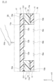
以下、図1A及び図1Bに基づいて、センサ装置1Aの構成を説明する。図1Aは本発明の第1実施形態のセンサ装置1Aの平面展開図であり、図1Bは図1Aに示す展開状態のものを組み立てたセンサ装置1AのIB-IB線に沿った断面図である。 Hereinafter, the configuration of the sensor device 1A will be explained based on FIGS. 1A and 1B. FIG. 1A is a plan development view of a sensor device 1A according to the first embodiment of the present invention, and FIG. 1B is a cross-sectional view taken along the line IB-IB of the sensor device 1A in which the sensor device 1A in the unfolded state shown in FIG. 1A is assembled. .

図1Aに示すように、センサ装置1Aは、絶縁性基材11と、センサ電極12(12a,12b,12c)と、第1シールド部13(131,132)と、検知電極14と、スペーサ15と、を備えている。 As shown in FIG. 1A, the sensor device 1A includes an insulating base material 11, sensor electrodes 12 (12a, 12b, 12c), a first shield part 13 (131, 132), a sensing electrode 14, and a spacer 15. It is equipped with.

同図に示す態様は一例であり、センサ電極12(12a,12b,12c)、第1シールド部13(131,132)、検知電極14の配置、数、形状は限定されない。例えば、同図では、検知電極14の数が2個の例を示しているが、検知電極14の数が1個でも3個以上でもよく、センサ電極12の数に合わせて検知電極14の数を3個としてもよい。或いは、絶縁性基材11の4隅に対応させて検知電極14を配置して、検知電極14の数を4個としてもよい。また、センサ装置1Aが、絶縁性基材11上に、センサ電極12及び検知電極14以外の電極パターン(例えば、スライダ電極やホイール電極等)を備えていてもよい。 The embodiment shown in the figure is an example, and the arrangement, number, and shape of the sensor electrodes 12 (12a, 12b, 12c), the first shield portion 13 (131, 132), and the detection electrode 14 are not limited. For example, although the figure shows an example in which the number of sensing electrodes 14 is two, the number of sensing electrodes 14 may be one, three or more, and the number of sensing electrodes 14 may be adjusted according to the number of sensor electrodes 12. may be three. Alternatively, the number of sensing electrodes 14 may be four by arranging the sensing electrodes 14 corresponding to the four corners of the insulating base material 11. Further, the sensor device 1A may include an electrode pattern (for example, a slider electrode, a wheel electrode, etc.) other than the sensor electrode 12 and the detection electrode 14 on the insulating base material 11.

本実施形態の絶縁性基材11は、図中X方向(図中横方向)に沿って領域A~Cを有している。図1Aに示すセンサ装置1Aにおいては、センサ電極12及び第1シールド部13は領域Bに形成され、検知電極14は領域A,Cのそれぞれに一つずつ形成されている。本実施形態の第1シールド部13は、センサ電極12の周囲に設けられるが、各センサ電極12a,12b,12cの間に延在させてもよい(図2Aを参照)。図1Aの平面展開図に示されるように、センサ電極12、第1シールド部13及び検知電極14は、絶縁性基材11の同一の主面11aに形成されている。 The insulating base material 11 of this embodiment has regions A to C along the X direction in the figure (horizontal direction in the figure). In the sensor device 1A shown in FIG. 1A, the sensor electrode 12 and the first shield part 13 are formed in region B, and one detection electrode 14 is formed in each of regions A and C. Although the first shield part 13 of this embodiment is provided around the sensor electrode 12, it may be extended between each of the sensor electrodes 12a, 12b, and 12c (see FIG. 2A). As shown in the plan development view of FIG. 1A, the sensor electrode 12, the first shield part 13, and the detection electrode 14 are formed on the same main surface 11a of the insulating base material 11.

なお、図1Aに示す例では、図中X方向がセンサ装置1Aの長手方向と一致しているセンサ装置1Aを例にして説明するが、図中Y方向がセンサ装置1Aの長手方向と一致するようにセンサ装置1Aを作製してもよい。また、センサ電極12及び第1シールド部13を絶縁性基材11の一方主面に形成し、検知電極14を絶縁性基材の他方主面に形成してもよい。 In addition, in the example shown in FIG. 1A, the explanation will be made using a sensor device 1A in which the X direction in the figure corresponds to the longitudinal direction of the sensor device 1A, but the Y direction in the figure corresponds to the longitudinal direction of the sensor device 1A. The sensor device 1A may be manufactured as follows. Moreover, the sensor electrode 12 and the first shield part 13 may be formed on one main surface of the insulating base material 11, and the sensing electrode 14 may be formed on the other main surface of the insulating base material.

本実施形態のセンサ装置1Aにおいて、センサ電極12と第1シールド部13とがタッチセンサTSを形成し、シールド電極131と検知電極14とが感圧センサを形成している。感圧センサを形成しているシールド電極131は、タッチセンサTSを形成している第1シールド部13の一部でもある。本実施形態では、タッチセンサTSにおける第1シールド部13の一部であるシールド電極131が、感圧センサの検知電極14と対をなす電極の機能を兼ねている。 In the sensor device 1A of this embodiment, the sensor electrode 12 and the first shield part 13 form a touch sensor TS, and the shield electrode 131 and the detection electrode 14 form a pressure-sensitive sensor. The shield electrode 131 forming the pressure sensitive sensor is also a part of the first shield part 13 forming the touch sensor TS. In this embodiment, the shield electrode 131, which is a part of the first shield part 13 in the touch sensor TS, also functions as an electrode that pairs with the detection electrode 14 of the pressure-sensitive sensor.

図1Aに示すセンサ装置1Aは、領域Aと領域Bとの間、つまり領域Aと領域Bとが連なる接続部分に所定領域Rを有している。同様に、センサ装置1Aは、領域Bと領域Cとの間、つまり領域Bと領域Cとが連なる接続部分に所定領域Rを有している。 A sensor device 1A shown in FIG. 1A has a predetermined region R between region A and region B, that is, at a connecting portion where region A and region B are continuous. Similarly, the sensor device 1A has a predetermined region R between region B and region C, that is, at a connecting portion where region B and region C are continuous.

この二つの所定領域Rは、それぞれ折り曲げ部Fを含んでいる。領域Aは、領域B側に折り曲げられる。本実施形態の折り曲げ部Fは、X軸に沿って異なる位置に設けられたY軸に沿った二本の折れ曲げ線L1,L2を含む。図中左側の領域Aについては、折り曲げ線L1及び/又はL2に沿って、または折り曲げ線L1又はL2の近傍で、Y軸に沿って(Y軸を中心に)折り曲げられる。絶縁性基材11は可撓性を備えた薄いシート状であるため、折り曲げられた折り曲げ部Fは曲面状となる。 These two predetermined regions R each include a bent portion F. Region A is bent toward region B. The bending portion F of this embodiment includes two bending lines L1 and L2 along the Y-axis provided at different positions along the X-axis. The region A on the left side of the figure is bent along the Y-axis (with the Y-axis as the center) along the bending line L1 and/or L2 or in the vicinity of the bending line L1 or L2. Since the insulating base material 11 is in the form of a thin sheet with flexibility, the bent portion F has a curved surface shape.

この折り曲げ動作により、折り曲げられた領域Aは領域Bと略面平行の位置関係となり、領域Aと領域Bが重なり、領域Aに形成された検知電極14とシールド電極131とが対向配置された状態となる。同様に、領域Cも、領域Cが領域Bに重なるように折り曲げられる。この折り曲げ動作により、折り曲げられた領域Cは領域Bと略面平行の位置関係となり、領域Cと領域Bが重なり、領域Cに形成された検知電極14とシールド電極131とが対向配置された状態となる。こうした折り曲げ動作により、センサ装置1Aが組み立てられる。組み立てられたセンサ装置1Aの断面を図1Bに示す。 Due to this bending operation, the bent area A becomes in a positional relationship that is substantially parallel to the plane of the area B, so that the area A and the area B overlap, and the sensing electrode 14 formed in the area A and the shield electrode 131 are placed facing each other. becomes. Similarly, region C is also folded so that region C overlaps region B. Due to this bending operation, the bent area C becomes in a positional relationship that is substantially parallel to the plane of the area B, so that the area C and the area B overlap, and the sensing electrode 14 and the shield electrode 131 formed in the area C are arranged to face each other. becomes. Through such a bending operation, the sensor device 1A is assembled. A cross section of the assembled sensor device 1A is shown in FIG. 1B.

図1Bに示すように、組み立てられたセンサ装置1Aにおいては、センサ電極12と第1シールド部13とは、第1面15aに設けられている(形成されている)。この第1面15aは、センサ装置1Aに対して入力操作等が行われる操作面側に配置されている。これに対し、検知電極14は、第2面15bに設けられている(形成されている)。この第2面15bは、第1面15aに対して、指などの操作子FINが接近又は接触する操作面側から-Z方向(図中上側を+Z方向と定義した場合における図中下側)の位置に配置されている。従って、第1面15aの方が第2面15bよりも操作面側に位置する。 As shown in FIG. 1B, in the assembled sensor device 1A, the sensor electrode 12 and the first shield portion 13 are provided (formed) on the first surface 15a. This first surface 15a is arranged on the operation surface side on which input operations and the like are performed on the sensor device 1A. On the other hand, the sensing electrode 14 is provided (formed) on the second surface 15b. This second surface 15b is located in the -Z direction (the lower side in the figure when the upper side in the figure is defined as the +Z direction) from the operation surface side where the operator FIN such as a finger approaches or contacts the first surface 15a. It is located at the position of Therefore, the first surface 15a is located closer to the operation surface than the second surface 15b.

ここで、操作面側とは、センサ装置1Aにおいて、指などの人体を含む操作子FINの接近又は接触による入力操作が行われる操作面に近い方(近い側)の位置を示す。第1面15aと第2面15bとは、図中Z方向で示すセンサ装置1Aの厚さ方向の位置(高さ)が異なる。第1面15aの位置の方が、第2面15bの位置よりも操作面に近い。 Here, in the sensor device 1A, the operation surface side refers to a position closer to the operation surface (closer side) where an input operation is performed by approaching or touching the operator FIN, which includes a human body such as a finger. The first surface 15a and the second surface 15b are different in position (height) in the thickness direction of the sensor device 1A shown in the Z direction in the figure. The position of the first surface 15a is closer to the operation surface than the position of the second surface 15b.

この第1面15a及び第2面15bは、センサ装置1A中のXY面に平行な仮想上の平面であり、本実施形態では、説明の便宜上、第1面15aと第2面15bの位置をスペーサ15の表裏面の位置を基準として設けた例を示す。しかしながら、第1面15aと第2面15bの位置を設定するための基準は、特にスペーサ15の表裏面に限定されない。例えば、絶縁性基材11の一方主面又は他方主面の位置を基準として、第1面15aと第2面15bの設定位置を定義してもよい。或いは、スペーサ15や絶縁性基材11に沿って設けられた他の部材の一方主面又は他方主面の位置を基準として、第1面15aと第2面15bの設定位置を定義してもよい。本実施形態における第1面15aと第2面15bは、センサ装置1Aを構成する何れかの部材のXY面に沿った面であり、Z座標値が異なる面である。 The first surface 15a and the second surface 15b are virtual planes parallel to the XY plane in the sensor device 1A, and in this embodiment, for convenience of explanation, the positions of the first surface 15a and the second surface 15b are An example is shown in which the positions of the front and back surfaces of the spacer 15 are provided as a reference. However, the reference for setting the positions of the first surface 15a and the second surface 15b is not particularly limited to the front and back surfaces of the spacer 15. For example, the set positions of the first surface 15a and the second surface 15b may be defined based on the position of one principal surface or the other principal surface of the insulating base material 11. Alternatively, the set positions of the first surface 15a and the second surface 15b may be defined based on the position of one principal surface or the other principal surface of the spacer 15 or other member provided along the insulating base material 11. good. The first surface 15a and the second surface 15b in this embodiment are surfaces along the XY plane of any member constituting the sensor device 1A, and have different Z coordinate values.

センサ装置1Aにおいて、第1面15aの方が第2面15bよりも操作面側に位置しているのであれば、第1面15aと第2面15bの形成方法は限定されない。例えば、図1Aのように、センサ電極12及び第1シールド部13を絶縁性基材11の一方の主面の領域Bに形成し、検知電極14を絶縁性基材11の一方の主面の領域A,Cに形成し、図1Bのように、センサ電極12及び第1シールド部13と検知電極14との間に絶縁性基材11が介在しないように折り曲げることで、第1面15aと第2面15bを形成してもよい。 In the sensor device 1A, the method of forming the first surface 15a and the second surface 15b is not limited as long as the first surface 15a is located closer to the operation surface than the second surface 15b. For example, as shown in FIG. 1A, the sensor electrode 12 and the first shield part 13 are formed in region B of one main surface of the insulating base material 11, and the sensing electrode 14 is formed in the region B of one main surface of the insulating base material 11. As shown in FIG. 1B, the first surface 15a and A second surface 15b may also be formed.

或いは、特に図示しないが、絶縁性基材11を逆側に折り曲げて、センサ電極12及び第1シールド部13の検知電極14側、及び、検知電極14のセンサ電極12及び第1シールド部13側に絶縁性基材11が介在するように第1面15aと第2面15bを形成してもよい。この場合においても、操作面を基準にすると、図中、Z軸方向に沿って、操作面、センサ電極12を含むタッチセンサTS(第1面15a)、検知電極14(第2面15b)の順で配置される。 Alternatively, although not particularly shown, the insulating base material 11 is bent to the opposite side, and the sensor electrode 12 and the first shield part 13 are placed on the sensing electrode 14 side, and the sensing electrode 14 is placed on the sensor electrode 12 and the first shield part 13 side. The first surface 15a and the second surface 15b may be formed such that the insulating base material 11 is interposed therebetween. In this case as well, based on the operation surface, the operation surface, the touch sensor TS including the sensor electrode 12 (first surface 15a), and the sensing electrode 14 (second surface 15b) are aligned along the Z-axis direction in the figure. arranged in order.

また、第1面15aと第2面15bとは、異なる絶縁性基材11の主面に形成してもよい。つまり、センサ電極12と第1シールド部13とが形成された絶縁性基材11と、検知電極14が形成された絶縁性基材11とが異なる基材であってもよい。 Further, the first surface 15a and the second surface 15b may be formed on different main surfaces of the insulating base material 11. That is, the insulating base material 11 on which the sensor electrode 12 and the first shield part 13 are formed and the insulating base material 11 on which the sensing electrode 14 is formed may be different base materials.

図1Aに示すセンサ装置1Aの折り曲げ部Fは、絶縁性基材11の図中Y軸方向に沿った領域を切り欠いて形成されている。つまり、折り曲げ部FのY軸方向に沿った長さ(図中Hと垂直方向の長さ)が、領域AのY軸方向に沿った長さよりも短くなるように形成されている。折り曲げ部FのY軸方向に沿った長さは、折り曲げ線に沿った長さである。 The bent portion F of the sensor device 1A shown in FIG. 1A is formed by cutting out a region of the insulating base material 11 along the Y-axis direction in the figure. That is, the length of the bent portion F along the Y-axis direction (the length in the direction perpendicular to H in the figure) is shorter than the length of the region A along the Y-axis direction. The length of the folded portion F along the Y-axis direction is the length along the fold line.

折り曲げ部FのY軸方向に沿った長さを、領域AのY軸方向の長さよりも短くすることにより、折り曲げ部Fで絶縁性基材11の可撓性が下がるので、絶縁性基材11を折り曲げやすくなり、折り曲げ作業(センサ装置1Aの組み立て作業)を簡易にできる。また、絶縁性基材11を折り曲げた後においては、折り曲げ部Fにかかる弾性力が低下するので、第1面15aと第2面15bの平行性を保ちやすくなる。図1Aに示す折り曲げ部Fの図中X軸方向に沿った長さHは、組み立て時における領域Bと領域Aの間の距離(領域Cと領域Bの間の距離)以上とすることが好ましい。 By making the length of the bent portion F along the Y-axis direction shorter than the length of the region A in the Y-axis direction, the flexibility of the insulating base material 11 at the bent portion F is reduced, so that the insulating base material 11 becomes easy to bend, and the bending work (assembling work of the sensor device 1A) can be simplified. Further, after the insulating base material 11 is bent, the elastic force applied to the bent portion F is reduced, so that it becomes easier to maintain parallelism between the first surface 15a and the second surface 15b. The length H of the folded portion F shown in FIG. 1A along the X-axis direction in the figure is preferably greater than or equal to the distance between region B and region A (distance between region C and region B) during assembly. .

図1Bに示すように、センサ装置1Aの表面(操作面/入力面)にはカバーパネル17を配置してもよい。カバーパネル17は、ポリカーボネート基材、アクリル基材、ガラス基材などの透明な材質で構成することが好ましい。 As shown in FIG. 1B, a cover panel 17 may be arranged on the surface (operation surface/input surface) of the sensor device 1A. The cover panel 17 is preferably made of a transparent material such as a polycarbonate base material, an acrylic base material, or a glass base material.

また、特に限定されないが、センサ装置1Aのカバーパネル17の配置位置とは反対側の位置(図中下側)には、ベース部材18を配置してもよい。ベース部材18は、センサ装置1Aと接触してセンサ装置1Aを支持してもよいし、センサ装置1Aと離間していてもよい。ベース部材18は、ポリエチレンテレフタレート(PET)、ポリイミド(PI)、液晶ポリマー(LCP)、ガラスエポキシ又はポリエチレンナフタレート(PEN)などのシート状の部材である。このベース部材18の絶縁性基材11側の面には発光体としてのLED16a,16b,16cを配置してもよい。 Further, although not particularly limited, the base member 18 may be arranged at a position opposite to the arrangement position of the cover panel 17 of the sensor device 1A (lower side in the figure). The base member 18 may be in contact with and support the sensor device 1A, or may be spaced apart from the sensor device 1A. The base member 18 is a sheet-like member made of polyethylene terephthalate (PET), polyimide (PI), liquid crystal polymer (LCP), glass epoxy, polyethylene naphthalate (PEN), or the like. LEDs 16a, 16b, and 16c as light emitters may be arranged on the surface of the base member 18 on the insulating base material 11 side.

図1Bに示すように、操作子FINがカバーパネル17に触れることにより信号(操作指令)が出力される。操作子FINの具体例としては、指やタッチペン等を例示することができる。カバーパネル17及びベース部材18は、接着剤や粘着テープを用いてセンサ装置1Aに接着することができる。特に限定されないが、接着剤や粘着テープの材料としては、アクリル樹脂系、ウレタン樹脂系、エポキシ樹脂系、シリコーン樹脂系等を用いることができる。なお、接着剤を、カバーパネル17、ベース部材18、或いはセンサ装置1Aに塗布して用いる場合には、接着剤を熱硬化、紫外線硬化、熱溶融させることで、これらを接着することができる。 As shown in FIG. 1B, when the operator FIN touches the cover panel 17, a signal (operation command) is output. Specific examples of the operator FIN include a finger, a touch pen, and the like. The cover panel 17 and the base member 18 can be adhered to the sensor device 1A using adhesive or adhesive tape. Although not particularly limited, acrylic resin, urethane resin, epoxy resin, silicone resin, etc. can be used as the material for the adhesive or adhesive tape. Note that when an adhesive is applied to the cover panel 17, the base member 18, or the sensor device 1A, these can be bonded by thermally curing, ultraviolet curing, or thermal melting the adhesive.

センサ電極12を含むタッチセンサTSの一態様として、タッチスイッチを例示することができる。また、センサ電極12を含むタッチセンサTSの別の態様として、タッチスイッチに代えて、タッチパネルを例示することができる。 A touch switch can be exemplified as one aspect of the touch sensor TS including the sensor electrode 12. Moreover, as another aspect of the touch sensor TS including the sensor electrode 12, a touch panel can be exemplified instead of a touch switch.

図1Bに示すように、絶縁性基材11の領域Bの主面11aが下側(カバーパネル17とは反対側の方向)に向くように配置され、屈曲された領域A及び領域Cの主面11aが上側(カバーパネル17側の方向)に向くように配置されている。領域Bの主面11aに形成されたセンサ電極12a,12b,12cは操作子FINとの間の静電容量の変化を検知する。センサ電極12a,12b,12cは、自己容量方式の一般的な静電容量センサの電極と同様の機能を備えている。 As shown in FIG. 1B, the main surface 11a of the region B of the insulating base material 11 is arranged so as to face downward (in the direction opposite to the cover panel 17), and the main surface 11a of the region A and the region C are bent. It is arranged so that the surface 11a faces upward (toward the cover panel 17 side). Sensor electrodes 12a, 12b, and 12c formed on the main surface 11a of region B detect changes in capacitance between them and the operator FIN. The sensor electrodes 12a, 12b, and 12c have the same function as the electrodes of a general self-capacitance type capacitance sensor.

以下、センサ装置1Aの構成部材について説明する。 Hereinafter, the constituent members of the sensor device 1A will be explained.

絶縁性基材11は、ポリエチレンテレフタレート(PET)、ポリイミド(PI)、液晶ポリマー(LCP)又はポリエチレンナフタレート(PEN)などのシート状の基材である。本実施形態では、透明性が高く、可撓性を備えたポリエチレンテレフタレート(PET)を用いている。絶縁性基材11の厚さはどのような厚さでもよいが、折り曲げ性を考慮すると10[μm]~200[μm]とすることができる。 The insulating base material 11 is a sheet-like base material such as polyethylene terephthalate (PET), polyimide (PI), liquid crystal polymer (LCP), or polyethylene naphthalate (PEN). In this embodiment, polyethylene terephthalate (PET), which has high transparency and flexibility, is used. The thickness of the insulating base material 11 may be any thickness, but considering bendability, it can be set to 10 [μm] to 200 [μm].

図1Aに示すように、本実施形態のセンサ電極12、第1シールド部13、及び検知電極14は、絶縁性基材11の同一の主面11aに形成されている。本実施形態のセンサ電極12、第1シールド部13と検知電極14とは、それぞれ、絶縁性基材11の異なる主面に形成されていてもよい。例えば、センサ電極12と第1シールド部13を絶縁性基材11の一方主面に形成し、検知電極14を絶縁性基材11の他方主面に形成してもよい。 As shown in FIG. 1A, the sensor electrode 12, the first shield part 13, and the detection electrode 14 of this embodiment are formed on the same main surface 11a of the insulating base material 11. The sensor electrode 12, the first shield part 13, and the detection electrode 14 of this embodiment may be formed on different main surfaces of the insulating base material 11, respectively. For example, the sensor electrode 12 and the first shield part 13 may be formed on one main surface of the insulating base material 11, and the sensing electrode 14 may be formed on the other main surface of the insulating base material 11.

センサ電極12、第1シールド部13、及び検知電極14は、銀、銅、カーボンなどの導電性材料により形成されている。これらセンサ電極12と、第1シールド部13と、検知電極14は、出願時に知られているスクリーン印刷やグラビアオフセット印刷などの印刷法や、サブトラクティブ法、アディテブ法(フルアディティブ法又はセミアディティブ法のいずれでもよい)などの手法を用いて形成することができる。本実施形態においては、センサ電極12と、第1シールド部13と、検知電極14は、絶縁性基材11の同一の主面11aに形成されているので、一回の製造工程により同時に形成することができる。 The sensor electrode 12, the first shield part 13, and the detection electrode 14 are made of a conductive material such as silver, copper, or carbon. These sensor electrodes 12, first shield part 13, and detection electrodes 14 can be fabricated using printing methods such as screen printing and gravure offset printing known at the time of filing, subtractive methods, additive methods (full additive methods or semi-additive methods). It can be formed using any of the following methods. In this embodiment, the sensor electrode 12, the first shield part 13, and the detection electrode 14 are formed on the same main surface 11a of the insulating base material 11, so they are formed simultaneously in one manufacturing process. be able to.

センサ電極12は、第1センサ電極12aと、第2センサ電極12bと、第3センサ電極12cを含んでいる。第1センサ電極12aと、第2センサ電極12bと、第3センサ電極12cは、それぞれ、自己容量方式の静電容量センサであり、静電容量の変化を検知する。第1センサ電極12aに接続する引出配線121aと、第2センサ電極12bに接続する引出配線121bと、第3センサ電極12cに接続する引出配線121cは、外部の回路装置に接続される。 The sensor electrode 12 includes a first sensor electrode 12a, a second sensor electrode 12b, and a third sensor electrode 12c. The first sensor electrode 12a, the second sensor electrode 12b, and the third sensor electrode 12c are each self-capacitance type capacitance sensors, and detect changes in capacitance. A lead wire 121a connected to the first sensor electrode 12a, a lead wire 121b connected to the second sensor electrode 12b, and a lead wire 121c connected to the third sensor electrode 12c are connected to an external circuit device.

本実施形態の第1シールド部13は、同じく、絶縁性基材11の一方の主面11a上であって、センサ電極12の周囲の少なくとも一部に形成されている。センサ電極12の周囲に設けられたシールド電極131の数は限定されない。センサ電極12の周囲に設けられたシールド電極131を、離散的に配置してもよいし、センサ電極12を取り囲むように配置してもよい。第1シールド部13は、グランドや定電位に接続される。 The first shield portion 13 of this embodiment is similarly formed on one main surface 11a of the insulating base material 11 and at least in part around the sensor electrode 12. The number of shield electrodes 131 provided around the sensor electrode 12 is not limited. The shield electrode 131 provided around the sensor electrode 12 may be arranged discretely or may be arranged so as to surround the sensor electrode 12. The first shield section 13 is connected to ground or a constant potential.

第1シールド部13は、シールド電極131と、シールド電極131と接続されたシールド配線132と、を含んでいる。シールド配線132は、外部に引き出されてグランドや定電位に接続される。図1Aに示す例において、シールド電極131及びシールド配線132は、センサ電極12を取り囲むように配置されている。第1シールド部13は、センサ電極12と操作子FINとの間の静電容量を正確に検知できるようにノイズを排除する。これにより、タッチセンサTSに接近した操作子FIN以外の導電体との容量結合による誤検知を防止できる。 The first shield section 13 includes a shield electrode 131 and a shield wiring 132 connected to the shield electrode 131. The shield wiring 132 is drawn out to the outside and connected to ground or a constant potential. In the example shown in FIG. 1A, the shield electrode 131 and the shield wiring 132 are arranged to surround the sensor electrode 12. The first shield part 13 eliminates noise so that the capacitance between the sensor electrode 12 and the operator FIN can be accurately detected. This can prevent false detection due to capacitive coupling with conductors other than the operator FIN that are close to the touch sensor TS.

本実施形態の第1シールド部13は、センサ電極12の周囲に設けられるが、第1シールド部13の態様は限定されない。例えば、第1シールド部13が、各第1~第3センサ電極12a、12b、12cの間を延在するシールド配線133,134(図2Aを参照)を含んでいてもよい。この場合に、このシールド配線133,134に対向配置された検知電極14を配置してもよく、シールド配線133,134は、感圧センサの検知電極14と対をなす電極の機能を兼ねたシールド電極として機能する。 Although the first shield part 13 of this embodiment is provided around the sensor electrode 12, the aspect of the first shield part 13 is not limited. For example, the first shield portion 13 may include shield wires 133 and 134 (see FIG. 2A) extending between each of the first to third sensor electrodes 12a, 12b, and 12c. In this case, the detection electrodes 14 may be arranged to face the shield wirings 133, 134, and the shield wirings 133, 134 may serve as shields that also function as electrodes that are paired with the detection electrodes 14 of the pressure-sensitive sensor. Functions as an electrode.

また、図1Aに示す例では、線状のシールド配線132を設けているが、シールド配線132の形状は線状に限定されない。シールド電極131以外の第1シールド部13は、その態様・形状にかかわらずシールド配線として機能する。例えば、図示しないが、第1シールド部13は、第1センサ電極12aと、第2センサ電極12bと、第3センサ電極12cのそれぞれの全周囲と、絶縁性基材11の余白を埋めるように二次元的に配置してもよい。この場合において、シールド電極131を除く箇所(領域)のすべてがシールド配線となる。 Further, in the example shown in FIG. 1A, a linear shield wiring 132 is provided, but the shape of the shield wiring 132 is not limited to a linear shape. The first shield portion 13 other than the shield electrode 131 functions as a shield wiring regardless of its aspect and shape. For example, although not shown, the first shield part 13 is configured to fill the entire circumference of each of the first sensor electrode 12a, the second sensor electrode 12b, and the third sensor electrode 12c, and the margin of the insulating base material 11. It may be arranged two-dimensionally. In this case, the entire area (area) except for the shield electrode 131 becomes the shield wiring.

第1シールド部13は、銀、銅、カーボンなどの導電性材料により形成してもよい。シールド電極131は、図1Aに示すように網目形状に形成することが好ましい。シールド配線132も網目形状に形成してもよい。シールド電極131を網目形状に形成することにより、センサ電極12に対する操作子FINの入力操作を精度高く検知できる。 The first shield portion 13 may be formed of a conductive material such as silver, copper, or carbon. The shield electrode 131 is preferably formed into a mesh shape as shown in FIG. 1A. The shield wiring 132 may also be formed in a mesh shape. By forming the shield electrode 131 into a mesh shape, the input operation of the operator FIN to the sensor electrode 12 can be detected with high accuracy.

ここで、センサ電極12は、第1シールド部13も含めた周囲に存在する誘電体との間で発生する静電容量変化を検知することにより操作子FINの接触を検知する。第1シールド部13に含まれるシールド電極131を網目形状ではなく、塗りつぶした(ベタ)パターンとすると、センサ電極12と第1シールド部13との容量結合が大きくなりすぎて、操作子FINの接近に伴う静電容量値の変化を高精度で検出しにくくなる。 Here, the sensor electrode 12 detects the contact of the operator FIN by detecting a change in capacitance that occurs between the sensor electrode 12 and the surrounding dielectric material including the first shield part 13. If the shield electrode 131 included in the first shield part 13 has a solid pattern instead of a mesh shape, the capacitive coupling between the sensor electrode 12 and the first shield part 13 will become too large, causing the operator FIN to approach This makes it difficult to detect changes in capacitance value with high accuracy.

これに対し、本実施形態では、シールド電極131を網目形状で形成することにより、センサ電極12とシールド電極131の容量結合が少なくなり、操作子FINの接近に伴う静電容量値の変化を高精度で検出することができる。さらに、シールド配線132も網目形状で形成することにより、センサ電極12とシールド配線132の容量結合が少なくなり、操作子FINの接近に伴う静電容量値の変化を更に高精度で検出することができる。 In contrast, in this embodiment, by forming the shield electrode 131 in a mesh shape, the capacitive coupling between the sensor electrode 12 and the shield electrode 131 is reduced, and the change in capacitance value due to the approach of the operator FIN is enhanced. Can be detected with precision. Furthermore, by forming the shield wiring 132 in a mesh shape, capacitive coupling between the sensor electrode 12 and the shield wiring 132 is reduced, and changes in capacitance value due to the approach of the operator FIN can be detected with higher accuracy. can.

第1シールド部13は、上述の通り、シールド電極131を含む。本実施形態のシールド電極131は、単にシールド機能を果たすだけではなく、検知電極14と対を形成して感圧センサ(後述する)を構成する機能を備える。第1シールド部13において、シールド電極131を設けることにより、検知電極14との間に別のセンサ(後述する感圧センサ)を形成することができる。 The first shield section 13 includes the shield electrode 131 as described above. The shield electrode 131 of this embodiment not only functions as a shield, but also has the function of forming a pair with the detection electrode 14 to form a pressure sensor (described later). By providing the shield electrode 131 in the first shield portion 13, another sensor (a pressure-sensitive sensor to be described later) can be formed between the shield electrode 131 and the detection electrode 14.

本実施形態の検知電極14は、センサ電極12と同じく、絶縁性基材11の主面11a上に形成されている。また、検知電極14は、第1シールド部13よりも外側に形成されている。外側の位置は、図中X方向であってもよいし、図中Y方向であってもよい。本実施形態では、検知電極14は、シールド電極131の外縁131Eから図中のX方向に沿って所定領域Rを介在させた位置に形成される。なお、シールド電極131の外側の外縁131Eは、第1シールド部13の図中X方向に沿って中央(本実施形態では第2センサ電極12bの形成位置)に対して外側に位置している。検知電極14に接続する引出配線141は外部の回路装置に接続され、検知電極14の出力信号は当該回路装置に出力される。 The sensing electrode 14 of this embodiment is formed on the main surface 11a of the insulating base material 11, like the sensor electrode 12. Further, the detection electrode 14 is formed outside the first shield part 13. The outer position may be in the X direction in the figure or in the Y direction in the figure. In this embodiment, the sensing electrode 14 is formed at a position with a predetermined region R interposed therebetween from the outer edge 131E of the shield electrode 131 along the X direction in the figure. Note that the outer edge 131E of the shield electrode 131 is located on the outer side of the center of the first shield portion 13 along the X direction in the figure (the position where the second sensor electrode 12b is formed in this embodiment). The lead wire 141 connected to the sensing electrode 14 is connected to an external circuit device, and the output signal of the sensing electrode 14 is output to the circuit device.

本実施形態の検知電極14を、センサ電極12及び第1シールド部13が形成された絶縁性基材11の一方主面とは異なる他の主面に形成してもよい。或いは、検知電極14を、センサ電極12及び第1シールド部13が形成された絶縁性基材11とは別の絶縁性基材11に形成してもよい。 The sensing electrode 14 of this embodiment may be formed on another main surface different from the one main surface of the insulating base material 11 on which the sensor electrode 12 and the first shield part 13 are formed. Alternatively, the sensing electrode 14 may be formed on an insulating base material 11 different from the insulating base material 11 on which the sensor electrode 12 and the first shield part 13 are formed.

本実施形態の検知電極14は、銀、カーボン、銅などの導電性材料により塗りつぶされて形成されている。いわゆるベタ電極として検知電極14が形成されている。なお、ベタパターンに代えて、検知電極14を網目形状に形成してもよい。対となるシールド電極131を網目形状とし、検知電極14を塗りつぶした状態(非網目形状)とすることにより、感圧センサの検知精度を向上させることができる。 The sensing electrode 14 of this embodiment is filled with a conductive material such as silver, carbon, or copper. The detection electrode 14 is formed as a so-called solid electrode. Note that instead of a solid pattern, the sensing electrode 14 may be formed in a mesh shape. The detection accuracy of the pressure-sensitive sensor can be improved by forming the pair of shield electrodes 131 into a mesh shape and by leaving the sensing electrode 14 filled in (non-mesh shape).

先述したように、センサ電極12は、第1シールド部13も含めた周囲に存在する誘電体との間で発生する静電容量変化を検知することにより、操作子FINの接触を検知するので、容量結合を小さくするために、検知電極14を網目形状に形成することも一案である。しかしながら、感圧センサの精度向上の観点から検討すると、シールド電極131と検知電極14との間の静電容量を大きな値として得ることにもメリットがある。そのため、検知電極14を導電性材料で塗りつぶした態様(いわゆるベタパターン)とすることで、静電容量を増加させて、感圧センサの検知感度を上げることができる。 As mentioned above, the sensor electrode 12 detects the contact of the operator FIN by detecting the capacitance change that occurs between the sensor electrode 12 and the surrounding dielectric material including the first shield part 13. In order to reduce capacitive coupling, one idea is to form the sensing electrode 14 into a mesh shape. However, when considered from the viewpoint of improving the accuracy of the pressure-sensitive sensor, there is also an advantage in obtaining a large capacitance between the shield electrode 131 and the sensing electrode 14. Therefore, by forming the sensing electrode 14 in a manner in which it is filled with a conductive material (so-called solid pattern), the capacitance can be increased and the detection sensitivity of the pressure-sensitive sensor can be increased.

続いて、本実施形態のセンサ装置1Aの機能を説明する。本実施形態のセンサ装置1Aは、センサ電極12により形成されるタッチセンサTSと、検知電極14とシールド電極131により形成される感圧センサと、を有する。 Next, the functions of the sensor device 1A of this embodiment will be explained. The sensor device 1A of the present embodiment includes a touch sensor TS formed by a sensor electrode 12 and a pressure sensor formed by a sensing electrode 14 and a shield electrode 131.

タッチセンサTSは、センサ電極12(12a,12b,12c)により形成される。上述のように、このタッチセンサTSは、自己容量方式の静電容量センサである。操作子FINがセンサ電極12に接触すると、センサ電極12とグランドとの間の一定の静電容量(寄生容量)に新たな静電容量が追加されるので、タッチセンサTSは、その静電容量変化を検出することで、操作子FINの接触を検知する。タッチセンサTSは、センサ電極12a,12b,12が検知した結果として静電容量の変化値(Diff値)を出力する。シールド電極131及びシールド配線132を含む第1シールド部13は、ノイズを排除してセンサ電極12の検知精度を向上させる。 The touch sensor TS is formed by sensor electrodes 12 (12a, 12b, 12c). As described above, this touch sensor TS is a self-capacitance type capacitance sensor. When the operator FIN contacts the sensor electrode 12, a new capacitance is added to the constant capacitance (parasitic capacitance) between the sensor electrode 12 and the ground, so the touch sensor TS By detecting the change, the contact of the operator FIN is detected. The touch sensor TS outputs a capacitance change value (Diff value) as a result of detection by the sensor electrodes 12a, 12b, and 12. The first shield part 13 including the shield electrode 131 and the shield wiring 132 eliminates noise and improves the detection accuracy of the sensor electrode 12.

感圧センサは、検知電極14とシールド電極131とにより形成される。感圧センサは、検知電極14とシールド電極131との間の静電容量変化を検知する。感圧センサは、検知電極14が検知した結果として静電容量の変化値(Diff値)を出力する。感圧センサが出力する静電容量の変化値は、入力操作をする操作子FINの押圧力に応じて、検知電極14とシールド電極131が相対的に接近することに伴って変化した静電容量の値である。感圧センサが検知した静電容量の変化値が所定値以上であれば、その入力操作が所定値以上の押圧力を伴うと判断できる。 The pressure sensor is formed by a detection electrode 14 and a shield electrode 131. The pressure sensor detects a change in capacitance between the detection electrode 14 and the shield electrode 131. The pressure-sensitive sensor outputs a capacitance change value (Diff value) as a result of detection by the detection electrode 14. The capacitance change value output by the pressure sensor is the capacitance that changes as the sensing electrode 14 and the shield electrode 131 relatively approach each other in accordance with the pressing force of the operator FIN for input operation. is the value of If the capacitance change value detected by the pressure sensor is greater than or equal to a predetermined value, it can be determined that the input operation involves a pressing force greater than or equal to the predetermined value.

本実施形態のセンサ装置1Aは、操作子FINにより操作されるセンサ電極12と第1シールド部13とにより構成されるタッチセンサTSだけではなく、第1シールド部13のシールド電極131を感圧センサの一部としても兼用し、シールド電極131と検知電極14とにより構成される感圧センサを備える。 The sensor device 1A of the present embodiment not only includes a touch sensor TS composed of a sensor electrode 12 and a first shield section 13 that are operated by an operator FIN, but also uses a shield electrode 131 of the first shield section 13 as a pressure-sensitive sensor. It also serves as a part of the sensor, and includes a pressure-sensitive sensor composed of a shield electrode 131 and a detection electrode 14.

これにより、ユーザ(操作者)がセンサ装置1Aの操作面に接触したか否か及び接触した操作面の平面位置の信号をタッチセンサTSから得るだけではなく、感圧センサから出力された信号によりユーザが意思を持って入力した信号であることを判断できる。例えば、感圧センサの出力値が所定値以上である場合には、タッチセンサTSの出力値がユーザの意思に基づく操作であると判断し、感圧センサの出力値が所定値未満である場合には、タッチセンサTSの出力値がユーザの意思に基づく操作ではなく、意図しない接触であると判断することができる。 As a result, not only the signals of whether the user (operator) has touched the operation surface of the sensor device 1A and the planar position of the touched operation surface can be obtained from the touch sensor TS, but also the signals output from the pressure sensor can be used. It can be determined that the signal was intentionally input by the user. For example, if the output value of the pressure sensor is greater than or equal to a predetermined value, the output value of the touch sensor TS is determined to be an operation based on the user's intention, and if the output value of the pressure sensor is less than the predetermined value. In this case, it can be determined that the output value of the touch sensor TS is not an operation based on the user's intention, but an unintended contact.

このように、本実施形態のセンサ装置1Aは、出力された全信号の中から、ユーザの意思に基づく操作により入力された信号を判断(抽出)できる。つまり、意図せずにタッチパネルに接触してしまったことによる信号を入力信号ではないと判断(排除)できる。この結果、本実施形態のセンサ装置1Aは、ユーザによって意図されていない入力による誤検知を防止できる。 In this way, the sensor device 1A of the present embodiment can determine (extract) a signal input by an operation based on the user's intention from among all the output signals. In other words, a signal caused by unintentionally touching the touch panel can be determined (excluded) as not being an input signal. As a result, the sensor device 1A of this embodiment can prevent false detections due to inputs not intended by the user.

本実施形態では、図1Bに示すように、第1シールド部13のシールド電極131と検知電極14とはXY面に沿って平行に配置され、XY平面における少なくとも一部の領域の位置が共通/重複している。シールド電極131のZ座標値(図中高さ/厚さ方向の位置)と検知電極14のZ座標値(図中高さ/厚さ方向の位置)とは異なる。第1シールド部13のシールド電極131と検知電極14とは対向するように配置されている。 In this embodiment, as shown in FIG. 1B, the shield electrode 131 of the first shield part 13 and the sensing electrode 14 are arranged in parallel along the XY plane, and the position of at least a part of the area in the XY plane is common/ Overlapping. The Z coordinate value of the shield electrode 131 (position in the height/thickness direction in the figure) and the Z coordinate value (position in the height/thickness direction in the figure) of the sensing electrode 14 are different. The shield electrode 131 of the first shield part 13 and the detection electrode 14 are arranged to face each other.

本実施形態において、第1シールド部13が、タッチセンサTSのシールド機能を果たすとともに、第1シールド部13の一部であるシールド電極131が、検知電極14と対をなして感圧センサ(圧力センサ)の電極としての機能を果たす。 In this embodiment, the first shield part 13 fulfills the shielding function of the touch sensor TS, and the shield electrode 131, which is a part of the first shield part 13, forms a pair with the detection electrode 14 and serves as a pressure sensitive sensor (pressure sensor). (sensor) functions as an electrode.

また、シールド電極131を含む第1シールド部13が設けられた第1面15aを、検知電極14が設けられた第2面15bよりもセンサ装置1Aの操作面であるカバーパネル17側に配置することにより、操作子FINと検知電極14との容量結合を遮断することができるので、シールド電極131が操作子FINの接近による感圧センサの誤検知を防止する遮断体として機能する。 Further, the first surface 15a on which the first shield part 13 including the shield electrode 131 is provided is arranged closer to the cover panel 17, which is the operation surface of the sensor device 1A, than the second surface 15b on which the detection electrode 14 is provided. As a result, the capacitive coupling between the operator FIN and the detection electrode 14 can be interrupted, so that the shield electrode 131 functions as a shield that prevents false detection by the pressure sensor due to the approach of the operator FIN.

このように、本実施形態では、遮断体を別部材として追加するのではなく、感圧センサ(圧力センサ)の一方の電極として機能するシールド電極131が、遮断体としての機能をも担う。このため、感圧センサ(圧力センサ)と独立した遮断体を設ける必要がない。シールド電極131が、感圧センサ(圧力センサ)の一方の電極としての機能と、遮断体としての機能との両方を果たすので、部品点数の増加を抑制することができる。このため、センサ装置1Aの総厚を薄くしたり、当該センサ装置1Aの高コスト化を抑制することができる。 In this manner, in this embodiment, the shield electrode 131, which functions as one electrode of the pressure sensor (pressure sensor), also functions as a barrier, rather than adding the barrier as a separate member. Therefore, there is no need to provide a blocking body independent of the pressure sensor (pressure sensor). Since the shield electrode 131 functions both as one electrode of the pressure sensor (pressure sensor) and as a blocker, an increase in the number of parts can be suppressed. Therefore, the total thickness of the sensor device 1A can be reduced and the cost of the sensor device 1A can be suppressed from increasing.

同図に示すように、シールド電極131と検知電極14との間にはスペーサ15が配置されている。感圧センサにおいて、シールド電極131とスペーサ15を介して対向配置される検知電極14は、Z軸方向の押圧によるスペーサ15の変形に応じた静電容量の変化を検知する。スペーサ15の第1面15a側の面は、シールド電極131と接しており、スペーサ15の反対側の第2面15b側の面は検知電極14に接している。 As shown in the figure, a spacer 15 is arranged between the shield electrode 131 and the detection electrode 14. In the pressure-sensitive sensor, the sensing electrode 14, which is placed opposite to the shield electrode 131 with the spacer 15 interposed therebetween, detects a change in capacitance in response to deformation of the spacer 15 due to pressure in the Z-axis direction. The surface of the spacer 15 on the first surface 15 a side is in contact with the shield electrode 131 , and the surface on the opposite side of the spacer 15 on the second surface 15 b side is in contact with the sensing electrode 14 .

スペーサ15は弾性を有する材料から構成された弾性体である。特に限定されないが、スペーサ15としては、ウレタン、シリコーンなどのクッションフォーム等から構成された弾性体を利用できる。本実施形態では、温度特性が良好な発泡シリコーンを、スペーサ15として用いている。なお、本実施形態では、センサ電極12の部分の透光性を確保する観点から、センサ電極12が形成される領域にはスペーサ15を配置していない。 The spacer 15 is an elastic body made of an elastic material. Although not particularly limited, as the spacer 15, an elastic body made of a cushion foam such as urethane or silicone can be used. In this embodiment, foamed silicone having good temperature characteristics is used as the spacer 15. In this embodiment, the spacer 15 is not disposed in the region where the sensor electrode 12 is formed, from the viewpoint of ensuring the translucency of the sensor electrode 12 portion.

また、シールド電極131は、検知電極14を覆うように形成する。シールド電極131のXY座標における領域(図1A及び図1B参照)に、検知電極14のXY座標における領域(図1A及び図1B参照)が属している。同図に示すように、シールド電極131は、検知電極14に接していない。また、第1シールド部13に含まれるシールド電極131の幅d131(X方向の幅)は、検知電極14の幅d14(X方向の幅)よりも太い(幅の長さの値が大きい)ことが好ましい(d131>d14)。図中Y方向においても同様に、シールド電極131の長さy131(Y方向の長さ)は、検知電極14の長さy14(Y方向の長さ)よりも長い(幅の長さの値が大きい)ことが好ましい(y131>y14)。 Further, the shield electrode 131 is formed to cover the sensing electrode 14. The region of the sensing electrode 14 in the XY coordinates (see FIGS. 1A and 1B) belongs to the region of the shield electrode 131 in the XY coordinates (see FIGS. 1A and 1B). As shown in the figure, the shield electrode 131 is not in contact with the sensing electrode 14. Further, the width d131 (width in the X direction) of the shield electrode 131 included in the first shield part 13 is thicker (the value of the length of the width is larger) than the width d14 (width in the X direction) of the sensing electrode 14. is preferable (d131>d14). Similarly, in the Y direction in the figure, the length y131 (length in the Y direction) of the shield electrode 131 is longer than the length y14 (length in the Y direction) of the sensing electrode 14 (the value of the width is (y131>y14) is preferable.

本実施形態では、シールド電極131のX方向の幅が検知電極14のX方向の幅よりも大きく、シールド電極131のY方向の幅が検知電極14のY方向の幅よりも大きくなるように、シールド電極131と検知電極14の形状、大きさ、位置(組み立て時の位置)を設定している。このため、平面視において、シールド電極131が存在するXY領域に、検知電極14が存在するXY領域が含まれ、シールド電極131が検知電極14を覆っている。 In this embodiment, the width of the shield electrode 131 in the X direction is larger than the width of the sensing electrode 14 in the X direction, and the width of the shield electrode 131 in the Y direction is larger than the width of the sensing electrode 14 in the Y direction. The shape, size, and position (position at the time of assembly) of the shield electrode 131 and the detection electrode 14 are set. Therefore, in plan view, the XY region where the shield electrode 131 exists includes the XY region where the sensing electrode 14 exists, and the shield electrode 131 covers the sensing electrode 14.

シールド電極131は、図中XY平面において検知電極14を覆うことで、平面視において、検知電極がシールド電極131から露出する部分がなくなり、操作子FINと検知電極14との静電結合をより確実に防止することができる。さらに、シールド電極131は、検知電極14を覆いつつ、シールド電極131を、検知電極14よりも大きくすることで、操作子FINが検知電極とは重ならない位置に接近した場合においても、斜め方向における操作子FINと検知電極14との静電結合も防止することが可能となる。 By covering the sensing electrode 14 in the XY plane in the figure, the shield electrode 131 eliminates the exposed part of the sensing electrode from the shield electrode 131 in plan view, making the electrostatic coupling between the operator FIN and the sensing electrode 14 more reliable. can be prevented. Furthermore, by making the shield electrode 131 larger than the detection electrode 14 while covering the detection electrode 14, even when the operator FIN approaches a position where it does not overlap with the detection electrode, the shield electrode 131 can be used in an oblique direction. It is also possible to prevent electrostatic coupling between the operator FIN and the detection electrode 14.

≪第2実施形態≫
第2実施形態のセンサ装置1Bは、(a)絶縁性基材11が領域Cに代えて領域Dを有している点、及び、(b)第2シールド体20を備えている点で、第1実施形態と相違する。なお、第2実施形態のセンサ装置1Bの基本的構成は、第1実施形態のセンサ装置1Aの基本的構成と共通する。以下に、第2実施形態におけるセンサ装置1Bについて第1実施形態との相違点についてのみ説明し、第1実施形態と同様の構成である部分については同一符号を付してその説明を省略する。
≪Second embodiment≫
The sensor device 1B of the second embodiment has the following points: (a) the insulating base material 11 has a region D instead of the region C; and (b) the second shield body 20 is provided. This is different from the first embodiment. Note that the basic configuration of the sensor device 1B of the second embodiment is the same as the basic configuration of the sensor device 1A of the first embodiment. Below, only the differences from the first embodiment regarding the sensor device 1B in the second embodiment will be explained, and the same reference numerals will be given to the parts having the same configuration as in the first embodiment, and the explanation thereof will be omitted.

図2A及び図2Bに基づいて第2実施形態のセンサ装置1Bについて説明する。図2Aは本発明の第2実施形態のセンサ装置1Bの平面展開図であり、図2Bは図2Aに示す展開状態のものを組み立てたセンサ装置1BのIIB-IIB線に沿った断面図である。 A sensor device 1B according to the second embodiment will be described based on FIGS. 2A and 2B. FIG. 2A is a plan development view of a sensor device 1B according to a second embodiment of the present invention, and FIG. 2B is a sectional view taken along the IIB-IIB line of the sensor device 1B assembled from the sensor device 1B in the unfolded state shown in FIG. 2A. .

図2Aに示すように、センサ装置1Bは、絶縁性基材11と、センサ電極12(12a,12b,12c)と、第1シールド部13(131,132,133,134)と、検知電極14と、第2シールド部20と、スペーサ15と、を備えている。 As shown in FIG. 2A, the sensor device 1B includes an insulating base material 11, sensor electrodes 12 (12a, 12b, 12c), a first shield part 13 (131, 132, 133, 134), and a sensing electrode 14. , a second shield portion 20 , and a spacer 15 .

本実施形態の第1シールド部13は、センサ電極12の周囲に設けられていると共に、各センサ電極12a,12b,12cの間に延在するシールド配線133,134(図2Aを参照)を含んでいる。特に図示しないが、このシールド配線133,134に対向して検知電極14を配置してもよい。この場合には、シールド配線133,134は、タッチセンサTSのシールド配線として機能、感圧センサの検知電極14と対をなす電極の機能、及び、検知電極の遮断体としての機能を兼ねる。 The first shield part 13 of this embodiment is provided around the sensor electrode 12 and includes shield wiring 133, 134 (see FIG. 2A) extending between each sensor electrode 12a, 12b, 12c. I'm here. Although not particularly illustrated, the detection electrode 14 may be placed opposite the shield wirings 133 and 134. In this case, the shield wirings 133 and 134 function as shield wiring of the touch sensor TS, function as an electrode paired with the sensing electrode 14 of the pressure-sensitive sensor, and function as a shield for the sensing electrode.

本実施形態の第2シールド部20は、検知電極14が設けられた面と同一の第2面15bに設けられており、検知電極14の周囲の少なくとも一部に設けられている。図2A及び図2Bに示す例においては、第2シールド部20は、検知電極14の周囲を取り囲むように配置されている。この第2シールド部20は、外部に引き出されてグランドや定電位に接続される。図2Aに示す例においては、第2シールド部20は、第1シールド部13のシールド電極131と接続されている。なお、第2シールド部20は、外部に引き出されてグランドや定電位に接続可能である限り、第1シールド部13と接続されていなくてもよい。 The second shield portion 20 of this embodiment is provided on the same second surface 15b as the surface on which the sensing electrode 14 is provided, and is provided at least in part around the sensing electrode 14. In the example shown in FIGS. 2A and 2B, the second shield part 20 is arranged to surround the detection electrode 14. This second shield section 20 is drawn out to the outside and connected to ground or a constant potential. In the example shown in FIG. 2A, the second shield part 20 is connected to the shield electrode 131 of the first shield part 13. Note that the second shield part 20 does not need to be connected to the first shield part 13 as long as it can be drawn out to the outside and connected to ground or a constant potential.

図2Bに示すように、組み立てられたセンサ装置1Bにおいては、センサ電極12と第1シールド部13とは、センサ装置1Bに対して入力操作等が行われる操作面側の第1面15aに設けられている(形成されている)。これに対し、検知電極14と第2シールド部20は、第1面15aに対して操作面側とは反対側に位置する第2面15bに設けられている(形成されている)。 As shown in FIG. 2B, in the assembled sensor device 1B, the sensor electrode 12 and the first shield portion 13 are provided on the first surface 15a on the operation surface side where input operations and the like are performed on the sensor device 1B. being formed (formed). On the other hand, the detection electrode 14 and the second shield part 20 are provided (formed) on the second surface 15b located on the opposite side of the operation surface with respect to the first surface 15a.

本実施形態の絶縁性基材11は、図中X方向(図中横方向)に沿って領域A,B,Dを有している。領域DのX方向に沿った長さは、領域BのX方向に沿った長さよりも短い。領域DのX方向に沿った長さdDは、領域BのX方向に沿った長さdBから領域AのX方向に沿った長さdAを差し引いた長さに基づいて設定する。折り返される領域Aの端部AEと領域Dの端部DEとの間を距離dADとすることができる。この場合には、dD+dAD+dA=dBとなるように領域Dの長さdDを設定する。 The insulating base material 11 of this embodiment has regions A, B, and D along the X direction in the figure (horizontal direction in the figure). The length of region D along the X direction is shorter than the length of region B along the X direction. The length dD of the region D along the X direction is set based on the length obtained by subtracting the length dA of the region A along the X direction from the length dB of the region B along the X direction. The distance dAD can be set between the end AE of the region A and the end DE of the region D to be folded back. In this case, the length dD of the area D is set so that dD+dAD+dA=dB.

図2Aに示すセンサ装置1Bにおいては、センサ電極12及び第1シールド部13は、領域Bに形成されている。一方、検知電極14及び第2シールド部20は領域A,Dのそれぞれに一つずつ形成されている。図2Aの平面展開図に示されるように、センサ電極12、第1シールド部13、検知電極14及び第2シールド部20は、絶縁性基材11の同一の主面11aに形成されている。 In the sensor device 1B shown in FIG. 2A, the sensor electrode 12 and the first shield part 13 are formed in the region B. On the other hand, one sensing electrode 14 and one second shield part 20 are formed in each of regions A and D. As shown in the plan development view of FIG. 2A, the sensor electrode 12, the first shield part 13, the detection electrode 14, and the second shield part 20 are formed on the same main surface 11a of the insulating base material 11.

同図に示すセンサ装置1Bは、領域Aと領域Bとの間、つまり領域Aと領域Bとが連なる接続部分に所定領域Rを有する。同様に、センサ装置1Bは、領域Bと領域Dとの間、つまり領域Bと領域Dとが連なる接続部分に所定領域Rを有する。 The sensor device 1B shown in the figure has a predetermined region R between region A and region B, that is, at a connecting portion where region A and region B are continuous. Similarly, the sensor device 1B has a predetermined region R between region B and region D, that is, at a connecting portion where region B and region D are continuous.

この二つの所定領域Rは、それぞれ折り曲げ部Fを含む。本実施形態の折り曲げ部Fは、絶縁性基材11の図中Y軸方向に沿った領域を切り欠いて形成されており、X軸に沿って異なる位置に2本の折れ曲げ線L1,L2を含む。折れ曲げ線L1,L2近傍で折り曲げられた領域Aは領域Bと略面平行の位置となり、領域Aに形成された検知電極14とシールド電極131とが向かい合う。折れ曲げ線L1,L2近傍で折り曲げられた領域Dは領域Bと略面平行の位置関係となり、領域Dに形成された検知電極14とシールド電極131とが向かい合う。こうした折り曲げ動作によりセンサ装置1Bを組み立てる。組み立てられたセンサ装置1Bの断面を図2Bに示す。 These two predetermined regions R each include a bent portion F. The bending portion F of this embodiment is formed by cutting out a region of the insulating base material 11 along the Y-axis direction in the figure, and has two bending lines L1 and L2 at different positions along the X-axis. including. The region A bent near the bending lines L1 and L2 is in a position substantially parallel to the surface of the region B, and the sensing electrode 14 formed in the region A and the shield electrode 131 face each other. The region D bent near the bending lines L1 and L2 has a positional relationship substantially parallel to the surface of the region B, and the sensing electrode 14 and the shield electrode 131 formed in the region D face each other. The sensor device 1B is assembled by such a bending operation. A cross section of the assembled sensor device 1B is shown in FIG. 2B.

本実施形態においても、センサ装置1Bの表面(操作面/入力面)にカバーパネル17を配置する。絶縁性基材11の領域Dの主面11aには発光体としてのLED16a,16b,16cを配置してもよい。図2Bに示すように、操作子FINがカバーパネル17に触れることにより信号(操作指令)を入力する。 Also in this embodiment, the cover panel 17 is arranged on the surface (operation surface/input surface) of the sensor device 1B. On the main surface 11a of the region D of the insulating base material 11, LEDs 16a, 16b, and 16c as light emitters may be arranged. As shown in FIG. 2B, a signal (operation command) is input by touching the cover panel 17 with the operator FIN.

センサ電極12a,12b,12cは操作子FINとの間の静電容量の変化を検知する。センサ電極12a,12b,12cは、自己容量方式の一般的な静電容量センサの電極と同様の機能を備える。 The sensor electrodes 12a, 12b, 12c detect changes in capacitance between them and the operator FIN. The sensor electrodes 12a, 12b, and 12c have the same function as the electrodes of a general self-capacitance type capacitance sensor.

センサ電極12a,12b,12cは、操作子FINとの間の静電容量変化を検知するタッチセンサTSを構成し、検知結果として静電容量の変化値(Diff値)を出力する。検知電極14とシールド電極131は、検知電極14とシールド電極131との間の静電容量変化を検知する感圧センサを構成し、検知結果として静電容量の変化値(Diff値)を出力する。 The sensor electrodes 12a, 12b, and 12c constitute a touch sensor TS that detects a change in capacitance with the operator FIN, and outputs a capacitance change value (Diff value) as a detection result. The sensing electrode 14 and the shield electrode 131 constitute a pressure-sensitive sensor that detects a change in capacitance between the sensing electrode 14 and the shield electrode 131, and outputs a capacitance change value (Diff value) as a detection result. .

図2A及び図2Bに示す第2実施形態のセンサ装置1Bは、上述の第1実施形態のセンサ装置1Aと同様に、操作子FINとセンサ電極12とにより構成されるタッチセンサTSだけではなく、シールド電極131と検知電極14とにより構成される感圧センサを備えることにより、誤検知が抑制されたセンサ装置1Bを提供することができる。 Similarly to the sensor device 1A of the first embodiment described above, the sensor device 1B of the second embodiment shown in FIGS. 2A and 2B includes not only the touch sensor TS configured by the operator FIN and the sensor electrode 12. By including the pressure-sensitive sensor configured by the shield electrode 131 and the detection electrode 14, it is possible to provide the sensor device 1B in which false detection is suppressed.

また、本実施形態では、上述の第1実施形態と同様に、シールド電極131が、感圧センサの一方の電極としての機能と、遮断体としての機能との両方を果たすので、センサ装置1Bの部品点数の増加を抑制することができる。このため、センサ装置1Bの総厚を薄くしたり、当該センサ装置1Bの高コスト化を抑制することができる。 Furthermore, in this embodiment, similarly to the first embodiment described above, the shield electrode 131 functions both as one electrode of the pressure-sensitive sensor and as a blocker, so that It is possible to suppress an increase in the number of parts. Therefore, the total thickness of the sensor device 1B can be reduced and the cost of the sensor device 1B can be suppressed from increasing.

さらに、図2A及び図2Bに示す第2実施形態のセンサ装置1Bは、第2シールド部20が、検知電極14と同一の第2面15bであって検知電極14の周囲の少なくとも一部に設けられていることにより、ノイズを排除して検知電極14とシールド電極131との間の静電容量を正確に検知できるようにすることができる。 Further, in the sensor device 1B of the second embodiment shown in FIGS. 2A and 2B, the second shield portion 20 is provided on the same second surface 15b as the sensing electrode 14 and at least partially around the sensing electrode 14. By doing so, it is possible to eliminate noise and accurately detect the capacitance between the sensing electrode 14 and the shield electrode 131.

≪第3実施形態≫
図3Aは本発明の第3実施形態におけるセンサ装置を示す平面展開図であり、図3Bは図3AのIIIB-IIIB線に沿ったセンサ装置の断面図である。
≪Third embodiment≫
FIG. 3A is a developed plan view showing a sensor device according to a third embodiment of the present invention, and FIG. 3B is a cross-sectional view of the sensor device taken along line IIIB-IIIB in FIG. 3A.

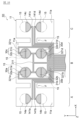
本実施形態では、(a)タッチセンサTSが相互容量方式の静電容量センサである点、(b)第1シールド部13が絶縁性基材11の領域Bの全面に設けられている点、及び、(c)2つの検知電極14a,14b(検知電極14c,14d)が絶縁性基材11の領域A(領域C)に2つずつ設けられている点で、第1実施形態と相違する。以下に、第3実施形態におけるセンサ装置1Cについて第1実施形態との相違点についてのみ説明し、第1実施形態と同様の構成である部分については同一符号を付してその説明を省略する。 In this embodiment, (a) the touch sensor TS is a mutual capacitance type capacitance sensor, (b) the first shield part 13 is provided on the entire surface of the region B of the insulating base material 11, and (c) is different from the first embodiment in that two sensing electrodes 14a, 14b (sensing electrodes 14c, 14d) are provided in each region A (region C) of the insulating base material 11. . Below, only the differences from the first embodiment regarding the sensor device 1C in the third embodiment will be explained, and the same reference numerals will be given to the parts having the same configuration as in the first embodiment, and the explanation thereof will be omitted.

本実施形態におけるセンサ装置1Cは、図3A及び図3Bに示すように、絶縁性基材11と、センサ電極30a~30cと、第1シールド部13と、検知電極14a~14dと、スペーサ15と、を備えている。 As shown in FIGS. 3A and 3B, the sensor device 1C in this embodiment includes an insulating base material 11, sensor electrodes 30a to 30c, a first shield part 13, sensing electrodes 14a to 14d, and a spacer 15. , is equipped with.

絶縁性基材11は、第1実施形態と同様に、図中X方向に沿って領域A~Cを有しており、領域Aと領域Bとの間に折り曲げ部Fを有していると共に、領域Bと領域Cとの間にも折り曲げ部Fを有している。そして、領域Aに2つの検知電極14a,14bが設けられ、領域Bにセンサ電極30a~30c及び第1シールド部13が設けられ、領域Cに2つの検知電極14c,14dが設けられている。図3Aに示すように、センサ電極30a~30c、第1シールド部13及び検知電極14a~14dは、絶縁性基材11の同一の主面11aに形成されている。 Similar to the first embodiment, the insulating base material 11 has regions A to C along the X direction in the figure, and has a bent portion F between region A and region B. , a bent portion F is also provided between region B and region C. Two sensing electrodes 14a and 14b are provided in region A, sensor electrodes 30a to 30c and the first shield portion 13 are provided in region B, and two sensing electrodes 14c and 14d are provided in region C. As shown in FIG. 3A, the sensor electrodes 30a to 30c, the first shield portion 13, and the detection electrodes 14a to 14d are formed on the same main surface 11a of the insulating base material 11.

3つのセンサ電極30a~30cは、図中X方向に沿って並べられている。そして、それぞれのセンサ電極30a~30cは、2つの電極から構成されている。具体的には、センサ電極30aは、入力電極(送信電極)(Tx)31aと受信電極(Rx)32aから構成されている。同様に、センサ電極30bも入力電極31bと受信電極32bから構成されており、センサ電極30cも入力電極31cと受信電極32cから構成されている。 The three sensor electrodes 30a to 30c are arranged along the X direction in the figure. Each of the sensor electrodes 30a to 30c is composed of two electrodes. Specifically, the sensor electrode 30a includes an input electrode (transmission electrode) (Tx) 31a and a reception electrode (Rx) 32a. Similarly, the sensor electrode 30b also includes an input electrode 31b and a receiving electrode 32b, and the sensor electrode 30c also includes an input electrode 31c and a receiving electrode 32c.

入力電極31a及び受信電極32aは、図中Y方向に沿って間隔を空けて相互に隣り合うように配置されている。本実施形態では、入力電極31a及び受信電極32aは、いずれも半円形状を有しており、センサ電極30aの全体の輪郭が略円形となるように、入力電極31a及び受信電極32aが配置されている。なお、入力電極31aと受信電極32aが間隔を空けて相互に隣り合うように配置されている限り、入力電極31a及び受信電極32aの形状は、特に上記に限定されない。例えば、入力電極31a及び受信電極32aの形状は、矩形状、或いは、櫛歯状であってもよい。 The input electrode 31a and the receiving electrode 32a are arranged adjacent to each other with an interval along the Y direction in the figure. In this embodiment, the input electrode 31a and the reception electrode 32a both have a semicircular shape, and are arranged so that the entire outline of the sensor electrode 30a is approximately circular. ing. Note that the shapes of the input electrode 31a and the reception electrode 32a are not particularly limited to the above, as long as the input electrode 31a and the reception electrode 32a are arranged adjacent to each other with an interval between them. For example, the shapes of the input electrode 31a and the receiving electrode 32a may be rectangular or comb-like.

センサ電極30bについても同様に、入力電極31b及び受信電極32bは、いずれも半円形状を有しており、センサ電極30bの全体の輪郭が略円形となるように配置されている。センサ電極30cについても同様に、入力電極31c及び受信電極32cは、いずれも半円形状を有しており、センサ電極30cの全体の輪郭が略円形となるように配置されている。 Similarly, for the sensor electrode 30b, the input electrode 31b and the reception electrode 32b both have a semicircular shape, and are arranged so that the overall outline of the sensor electrode 30b is approximately circular. Similarly, regarding the sensor electrode 30c, the input electrode 31c and the receiving electrode 32c both have a semicircular shape, and are arranged so that the overall outline of the sensor electrode 30c is approximately circular.

3つの入力電極31a~31cには、一本の引出配線311が分岐して接続されている。入力電極31a~31cは、この引出配線311を介して、外部の回路装置(不図示)に接続される。これに対し、3つの受信電極32a~32cには、3本の引出配線321a~321cがそれぞれ接続されている。この受信電極32a~32cは、引出配線321a~321cを介して、外部の回路装置に個別に接続される。 A single lead wire 311 is branched and connected to the three input electrodes 31a to 31c. The input electrodes 31a to 31c are connected to an external circuit device (not shown) via this lead wire 311. On the other hand, three lead wires 321a to 321c are connected to the three reception electrodes 32a to 32c, respectively. The receiving electrodes 32a to 32c are individually connected to external circuit devices via lead wires 321a to 321c.

本実施形態では、外部の回路装置から入力電極31aに電圧を印加することで、当該入力電極31aと受信電極32aとの間に電界を発生させる。そして、操作子FINが接近すると、上記の電界が変化すると共に電極31a,32a間の静電容量も変化するので、受信電極32aがその静電容量変化を検出することで、操作子FINの接触を検知する。なお、上述のように入力電極31aには外部の回路装置から電圧が印加されているので、操作子FINの接近によって当該入力電極31aの電位が変化することはない。 In this embodiment, an electric field is generated between the input electrode 31a and the receiving electrode 32a by applying a voltage to the input electrode 31a from an external circuit device. When the operator FIN approaches, the above electric field changes and the capacitance between the electrodes 31a and 32a also changes, so the receiving electrode 32a detects the change in capacitance, causing the contact of the operator FIN. Detect. Note that, as described above, since a voltage is applied to the input electrode 31a from an external circuit device, the potential of the input electrode 31a does not change due to the approach of the operator FIN.

センサ電極30bについても同様に、外部の回路装置から入力電極31bに電圧を印加して、当該入力電極31bと受信電極32bとの間に電界を発生させ、電極31b,32b間の静電容量変化を受信電極32bが検出することで、操作子FINの接触を検知する。センサ電極30cについても同様に、外部の回路装置から入力電極31cに電圧を印加して、当該入力電極31cと受信電極32cとの間に電界を発生させ、電極31c,32c間の静電容量変化を受信電極32cが検出することで、操作子FINの接触を検知する。 Similarly, regarding the sensor electrode 30b, a voltage is applied to the input electrode 31b from an external circuit device to generate an electric field between the input electrode 31b and the receiving electrode 32b, thereby changing the capacitance between the electrodes 31b and 32b. The receiving electrode 32b detects the contact of the operator FIN. Similarly, regarding the sensor electrode 30c, a voltage is applied to the input electrode 31c from an external circuit device to generate an electric field between the input electrode 31c and the receiving electrode 32c, thereby changing the capacitance between the electrodes 31c and 32c. The receiving electrode 32c detects the contact of the operator FIN.

本実施形態の第1シールド部13は、センサ電極30a~30cの周囲と引出配線311,321a~321cの周囲を除いて、絶縁性基材11の領域Bのほぼ全域に設けられている。この第1シールド部13は、図3Aに示すように網目形状を有しているが、特にこれに限定されず、第1シールド部13がベタパターンあってもよい。また、上述した第1実施形態のように、第1シールド部30の形状を、センサ電極30a~30cを取り囲むような枠形状としてもよい。 The first shield portion 13 of this embodiment is provided over almost the entire region B of the insulating base material 11, except for the surroundings of the sensor electrodes 30a to 30c and the lead wires 311, 321a to 321c. Although the first shield part 13 has a mesh shape as shown in FIG. 3A, the first shield part 13 is not particularly limited to this, and the first shield part 13 may have a solid pattern. Further, as in the first embodiment described above, the first shield portion 30 may have a frame shape that surrounds the sensor electrodes 30a to 30c.

本実施形態では、センサ電極30a~30cと引出配線311,321a~321cのレイアウトの関係上、第1シールド部13が4つの領域に分割されているが、個々の領域に引出配線135が個別に接続されており、この引出配線135を介して第1シールド部13がグランドや定電位に接続される。 In this embodiment, the first shield part 13 is divided into four regions due to the layout of the sensor electrodes 30a to 30c and the lead wires 311, 321a to 321c, but the lead wires 135 are individually arranged in each region. The first shield portion 13 is connected to the ground or a constant potential via this lead wire 135.

検知電極14a,14bは、絶縁性基材11の領域Aの図中Y方向の両端に配置されている。この2つの検知電極14a,14bには、一本の引出配線141が分岐して接続されている。検知電極14a,14bは、この引出配線141を介して、外部の回路装置に接続される。 The sensing electrodes 14a and 14b are arranged at both ends of the region A of the insulating base material 11 in the Y direction in the figure. A single lead wire 141 is branched and connected to these two sensing electrodes 14a and 14b. The detection electrodes 14a, 14b are connected to an external circuit device via this lead wire 141.

同様に、検知電極14c,14dも、絶縁性基材11の領域Cの図中Y方向の両端に配置されている。この2つの検知電極14c,14dには、一本の引出配線141が分岐して接続されている。検知電極14c,14dは、この引出配線141を介して、外部の回路装置に接続される。 Similarly, the detection electrodes 14c and 14d are also arranged at both ends of the region C of the insulating base material 11 in the Y direction in the figure. A single lead wire 141 is branched and connected to these two sensing electrodes 14c and 14d. The detection electrodes 14c and 14d are connected to an external circuit device via this lead wiring 141.

以上に説明したセンサ電極30a~30c、第1シールド部13、及び検知電極14a~14dは、第1実施形態で説明したセンサ電極12、第1シールド部13及び検知電極14と同様の材料及び製法により形成されている。 The sensor electrodes 30a to 30c, the first shield part 13, and the detection electrodes 14a to 14d described above are made of the same materials and manufactured by the same method as the sensor electrode 12, the first shield part 13, and the detection electrode 14 described in the first embodiment. It is formed by

第1実施形態と同様に、一方の折り曲げ部Fを折り曲げることで、スペーサ15を介して領域Aと領域Bが重なり、検知電極14a,14bが第1シールド部13の一部136(対向部分136)と対向する。同様に、他方の折り曲げ部Fを折り曲げることで、スペーサ15を介して領域Cと領域Bが重なり、検知電極14c,14dと第1シールド部13の一部136(対向部分136)と対向する。こうした折り曲げ動作により、センサ装置1Cが組み立てられる。組み立てられたセンサ装置1Cの断面を図3Bに示す。この状態において、センサ電極30a~30cと第1シールド部13とは、第1面15aに設けられているのに対し、検知電極14a~14dは、第2面15bに設けられている。 Similarly to the first embodiment, by bending one of the bent portions F, the regions A and B overlap with each other via the spacer 15, and the sensing electrodes 14a and 14b are connected to a portion 136 of the first shield portion 13 (opposing portion 136). ) to face. Similarly, by bending the other bent portion F, the regions C and B overlap with each other via the spacer 15, and face the sensing electrodes 14c, 14d and a portion 136 (opposing portion 136) of the first shield portion 13. Through such a bending operation, the sensor device 1C is assembled. A cross section of the assembled sensor device 1C is shown in FIG. 3B. In this state, the sensor electrodes 30a to 30c and the first shield portion 13 are provided on the first surface 15a, while the detection electrodes 14a to 14d are provided on the second surface 15b.

本実施形態では、センサ電極30a~30cと第1シールド部13がタッチセンサTSを形成している。具体的には、上述のように、センサ電極30a~30cは、静電容量変化を検知することにより、操作子FINの接触を検知する。この際、第1シールド部13は、センサ電極30a~30cと操作子FINとの間の静電容量を正確に検知できるようにノイズを排除する。 In this embodiment, the sensor electrodes 30a to 30c and the first shield portion 13 form a touch sensor TS. Specifically, as described above, the sensor electrodes 30a to 30c detect the contact of the operator FIN by detecting a change in capacitance. At this time, the first shield section 13 eliminates noise so that the capacitance between the sensor electrodes 30a to 30c and the operator FIN can be accurately detected.

また、本実施形態では、検知電極14a~14dと第1シールド部13の対向部分136が感圧センサを形成している。具体的には、操作子FINの押圧に伴って検知電極14aと対向部分136との間の間隔が狭まるので、検知電極14a~14dは、当該間隔の変化に応じた静電容量の変化を検知する。 Furthermore, in this embodiment, the sensing electrodes 14a to 14d and the opposing portion 136 of the first shield portion 13 form a pressure sensor. Specifically, as the distance between the sensing electrode 14a and the opposing portion 136 narrows as the operator FIN is pressed, the sensing electrodes 14a to 14d detect changes in capacitance in accordance with the change in the distance. do.

すなわち、本実施形態では、感圧センサを形成している対向部分136は、タッチセンサTSを形成している第1シールド部13の一部でもあり、タッチセンサTSにおける第1シールド部13の一部である対向部分136が、感圧センサの検知電極14a~14dと対をなす電極の機能を兼ねている。 That is, in this embodiment, the opposing portion 136 forming the pressure sensor is also a part of the first shield part 13 forming the touch sensor TS, and is a part of the first shield part 13 in the touch sensor TS. The opposing portion 136, which is a portion of the pressure-sensitive sensor, also functions as an electrode that pairs with the detection electrodes 14a to 14d of the pressure-sensitive sensor.

また、本実施形態では、第1シールド部13が設けられた第1面15aを、検知電極14a~14dが設けられた第2面15bよりもセンサ装置1Cの操作面側に配置することにより、操作子FINと検知電極14a~14dとの容量結合を遮断することができるので、第1シールド部13が操作子FINの接近による感圧センサの誤検知を防止する遮断体として機能する。 Furthermore, in this embodiment, by arranging the first surface 15a on which the first shield part 13 is provided closer to the operation surface of the sensor device 1C than the second surface 15b on which the sensing electrodes 14a to 14d are provided, Since the capacitive coupling between the operator FIN and the detection electrodes 14a to 14d can be interrupted, the first shield portion 13 functions as a shield that prevents false detection by the pressure sensor due to the approach of the operator FIN.

このように、本実施形態では、第1シールド部13が、感圧センサの一方の電極としての機能と、遮断体としての機能との両方を果たすので、部品点数の増加を抑制することができる。このため、センサ装置1Cの総厚を薄くしたり、当該センサ装置1Cの高コスト化を抑制することができる。 In this way, in the present embodiment, the first shield part 13 functions both as one electrode of the pressure-sensitive sensor and as a blocker, so it is possible to suppress an increase in the number of parts. . Therefore, it is possible to reduce the total thickness of the sensor device 1C and to suppress the increase in cost of the sensor device 1C.

≪第4実施形態≫
図4は本発明の第4実施形態におけるセンサ装置を示す平面展開図である。
≪Fourth embodiment≫
FIG. 4 is a developed plan view showing a sensor device according to a fourth embodiment of the present invention.

本実施形態では、遮断電極を備えている点で、第3実施形態と相違する。以下に、第4実施形態におけるセンサ装置1Dについて第3実施形態との相違点についてのみ説明し、第3実施形態と同様の構成である部分については同一符号を付してその説明を省略する。 This embodiment differs from the third embodiment in that it includes a cutoff electrode. Below, only the differences between the sensor device 1D in the fourth embodiment and the third embodiment will be explained, and the same reference numerals will be given to the parts having the same configuration as in the third embodiment, and the explanation thereof will be omitted.

本実施形態におけるセンサ装置1Dは、図4に示すように、絶縁性基材11、センサ電極30a~30c、第1シールド部13、検知電極14a~14d、及びスペーサ15に加えて、4つの遮断電極40a~40dを備えている。 As shown in FIG. 4, the sensor device 1D in this embodiment includes an insulating base material 11, sensor electrodes 30a to 30c, a first shield part 13, sensing electrodes 14a to 14d, and a spacer 15, as well as four interrupters. It includes electrodes 40a to 40d.

遮蔽電極40a~40dは、絶縁性基材11の領域Bに設けられている。この遮断電極40a~40dは、絶縁性基材11を折り曲げ部Fで折り曲げた状態において、検知電極14a~14dにそれぞれ対向するように、絶縁性基材11の主面11a上に配置されている。本実施形態では、遮蔽電極40a~40dが検知電極14a~14dよりも大きくなっており、絶縁性基材11を折り曲げ部Fで折り曲げた状態において、遮蔽電極40a~40dが検知電極14a~14dを覆っている。4つの遮断電極40a~40dは、センサ電極30a~30cの入力電極31a~31cを接続する引出配線311によって接続されており、当該入力電極31a~31cと同電位となっている。 Shield electrodes 40a to 40d are provided in region B of insulating base material 11. The cutoff electrodes 40a to 40d are arranged on the main surface 11a of the insulating base material 11 so as to face the detection electrodes 14a to 14d, respectively, when the insulating base material 11 is bent at the bending portion F. . In this embodiment, the shielding electrodes 40a to 40d are larger than the sensing electrodes 14a to 14d, and when the insulating base material 11 is bent at the bending part F, the shielding electrodes 40a to 40d are larger than the sensing electrodes 14a to 14d. covered. The four cutoff electrodes 40a to 40d are connected by a lead wire 311 that connects the input electrodes 31a to 31c of the sensor electrodes 30a to 30c, and have the same potential as the input electrodes 31a to 31c.

この遮断電極40a~40dは、第1実施形態で説明したセンサ電極12、第1シールド部13及び検知電極14と同様の材料及び製法により形成されている。なお、本実施形態の第1シールド部13は、センサ電極30a~30cの及び引出配線311,321a~321cに加えて、この遮断電極40a~40dの周囲にも形成されていない。 The cutoff electrodes 40a to 40d are formed using the same material and manufacturing method as the sensor electrode 12, first shield portion 13, and detection electrode 14 described in the first embodiment. Note that the first shield portion 13 of this embodiment is not formed around the cutoff electrodes 40a to 40d, in addition to the sensor electrodes 30a to 30c and the lead wires 311, 321a to 321c.

本実施形態では、センサ電極30a~30cと第1シールド部13がタッチセンサTSを形成している。また、本実施形態では、検知電極14a~14dと遮断電極40a~40dが感圧センサを形成している。 In this embodiment, the sensor electrodes 30a to 30c and the first shield portion 13 form a touch sensor TS. Further, in this embodiment, the detection electrodes 14a to 14d and the cutoff electrodes 40a to 40d form a pressure sensor.

そして、特に図示しないが、第3実施形態の図3Bと同様に、遮断電極40a~40dが設けられた第1面15aを、検知電極14a~14dが設けられた第2面15bよりもセンサ装置1Dの操作面側に配置すると共に、遮断電極40a~40dが入力電極31a~31cに接続されて当該入力電極31a~31cと同電位となっている。これにより、操作子FINと検知電極14a~14dとの容量結合を遮断することができるので、遮断電極40a~40dが操作子FINの接近による感圧センサの誤検知を防止する遮断体として機能する。 Although not particularly illustrated, similarly to FIG. 3B of the third embodiment, the first surface 15a provided with the cutoff electrodes 40a to 40d is placed closer to the sensor device than the second surface 15b provided with the detection electrodes 14a to 14d. The cutoff electrodes 40a to 40d are arranged on the operation surface side of the 1D, and are connected to the input electrodes 31a to 31c to have the same potential as the input electrodes 31a to 31c. As a result, the capacitive coupling between the operator FIN and the detection electrodes 14a to 14d can be interrupted, so the interrupting electrodes 40a to 40d function as an interrupter that prevents false detection by the pressure sensor due to the approach of the operator FIN. .

このように、本実施形態では、遮断電極40a~40dが、感圧センサの一方の電極としての機能と、遮断体としての機能との両方を果たすので、部品点数の増加を抑制することができる。このため、センサ装置1Dの総厚を薄くしたり、当該センサ装置1Dの高コスト化を抑制することができる。 In this way, in this embodiment, the cutoff electrodes 40a to 40d function both as one electrode of the pressure-sensitive sensor and as a cutoff body, so it is possible to suppress an increase in the number of parts. . Therefore, it is possible to reduce the total thickness of the sensor device 1D and to suppress the increase in cost of the sensor device 1D.

≪第5実施形態≫
図5は本発明の第5実施形態におけるセンサ装置を示す平面展開図である。
≪Fifth embodiment≫
FIG. 5 is a developed plan view showing a sensor device according to a fifth embodiment of the present invention.

本実施形態では、遮断電極が引出配線を介して入力電極に直接接続されていない点で、第4実施形態と相違する。以下に、第5実施形態におけるセンサ装置1Eについて第4実施形態との相違点についてのみ説明し、第4実施形態と同様の構成である部分については同一符号を付してその説明を省略する。 This embodiment differs from the fourth embodiment in that the cutoff electrode is not directly connected to the input electrode via the lead wire. Below, only the differences between the sensor device 1E in the fifth embodiment and the fourth embodiment will be explained, and the same reference numerals will be given to the parts having the same configuration as in the fourth embodiment, and the explanation thereof will be omitted.

本実施形態では、遮断電極40a~40dに、入力電極31a~31cを接続する引出配線311が接続されていない。遮断電極40a~40dには、引出配線311とは別の引出配線41が接続されており、この引出配線41を介して、外部の回路装置に接続される。この際、外部の回路装置によって、4つの遮断電極40a~40dに電圧が印加され、当該遮断電極40a~40dがセンサ電極30a~30cの入力電極31a~31cの電位と実質的に同一の電位を有する(すなわち、遮断電極40a~40dが入力電極31a~31cと同電位となる)ように構成されている。 In this embodiment, the extraction wiring 311 that connects the input electrodes 31a to 31c is not connected to the cutoff electrodes 40a to 40d. A lead wire 41 different from the lead wire 311 is connected to the cutoff electrodes 40a to 40d, and connected to an external circuit device via the lead wire 41. At this time, a voltage is applied to the four cutoff electrodes 40a to 40d by an external circuit device, and the cutoff electrodes 40a to 40d have substantially the same potential as the potential of the input electrodes 31a to 31c of the sensor electrodes 30a to 30c. (that is, the cutoff electrodes 40a to 40d have the same potential as the input electrodes 31a to 31c).

上述の第4実施形態と同様に、本実施形態では、遮断電極40a~40dが設けられた第1面15aを、検知電極14a~14dが設けられた第2面15bよりもセンサ装置1Dの操作面側に配置すると共に、遮断電極40a~40dの電位が入力電極31a~31cの電位と実質的に同一となるように構成されている。これにより、操作子FINと検知電極14a~14dとの容量結合を遮断することができるので、遮断電極40a~40dが操作子FINの接近による感圧センサの誤検知を防止する遮断体として機能する。 Similar to the fourth embodiment described above, in this embodiment, the first surface 15a on which the cutoff electrodes 40a to 40d are provided is easier to operate the sensor device 1D than the second surface 15b on which the detection electrodes 14a to 14d are provided. The cutoff electrodes 40a to 40d are arranged on the surface side, and the potentials of the cutoff electrodes 40a to 40d are substantially the same as the potentials of the input electrodes 31a to 31c. As a result, the capacitive coupling between the operator FIN and the detection electrodes 14a to 14d can be interrupted, so the interrupting electrodes 40a to 40d function as an interrupter that prevents false detection by the pressure sensor due to the approach of the operator FIN. .

このように、本実施形態では、遮断電極40a~40dが、感圧センサの一方の電極としての機能と、遮断体としての機能との両方を果たすので、部品点数の増加を抑制することができる。このため、センサ装置1Eの総厚を薄くしたり、当該センサ装置1Eの高コスト化を抑制することができる。 In this way, in this embodiment, the cutoff electrodes 40a to 40d function both as one electrode of the pressure-sensitive sensor and as a cutoff body, so it is possible to suppress an increase in the number of parts. . Therefore, the total thickness of the sensor device 1E can be reduced, and the cost increase of the sensor device 1E can be suppressed.

≪第6実施形態≫
図6Aは本発明の第6実施形態におけるセンサ装置を示す平面展開図であり、図6Bは図6Aに示すセンサ装置の領域A,Cを折り曲げた状態を示す平面図であり、図6Cは図6BのVIC-VIC線に沿ったセンサ装置の断面図である。
≪Sixth embodiment≫
FIG. 6A is a plan view showing a sensor device according to a sixth embodiment of the present invention, FIG. 6B is a plan view showing a state in which regions A and C of the sensor device shown in FIG. 6A are bent, and FIG. FIG. 6B is a cross-sectional view of the sensor device along the line VIC-VIC of FIG.

本実施形態では、(a)4つのセンサ電極12a~12dがマトリクス状に配置されている点、(b)第1シールド部13が絶縁性基材11の領域Bの全面に設けられている点、(c)2つの検知電極14a,14b(検知電極14c,14d)が絶縁性基材11の領域A(領域C)に2つずつ設けられている点、及び、(d)第2シールド部20が絶縁性基材11の領域A(領域C)に設けられている点で、第1実施形態と相違する。以下に、第6実施形態におけるセンサ装置1Fについて第1実施形態との相違点についてのみ説明し、第1実施形態と同様の構成である部分については同一符号を付してその説明を省略する。 In this embodiment, (a) four sensor electrodes 12a to 12d are arranged in a matrix, and (b) the first shield part 13 is provided over the entire area B of the insulating base material 11. , (c) two sensing electrodes 14a, 14b (sensing electrodes 14c, 14d) are provided in each region A (region C) of the insulating base material 11, and (d) the second shield portion. 20 is provided in region A (region C) of the insulating base material 11, which is different from the first embodiment. Below, only the differences between the sensor device 1F in the sixth embodiment and the first embodiment will be explained, and the same reference numerals will be given to the parts having the same configuration as in the first embodiment, and the explanation thereof will be omitted.

本実施形態のセンサ電極12a~12dは、第1実施形態のセンサ電極12a~12cと同様に、自己容量方式の静電容量センサである。図6Aに示すように、4つのセンサ電極12a~12dは、絶縁性基材11の主面11a上に設けられており、2行2列に配列されている。センサ電極12a~12dには、4本の引出配線121a~121dがそれぞれ接続されており、このセンサ電極12a~12dは、引出配線121a~121dを介して、外部の回路装置に個別に接続される。 The sensor electrodes 12a to 12d of this embodiment are self-capacitance type capacitance sensors like the sensor electrodes 12a to 12c of the first embodiment. As shown in FIG. 6A, four sensor electrodes 12a to 12d are provided on the main surface 11a of the insulating base material 11 and arranged in two rows and two columns. Four lead wires 121a to 121d are connected to the sensor electrodes 12a to 12d, respectively, and the sensor electrodes 12a to 12d are individually connected to external circuit devices via the lead wires 121a to 121d. .

検知電極14a,14bは、絶縁性基材11の領域Aの図中Y方向の両端に配置されている。この2つの検知電極14a,14bには、一本の引出配線141が分岐して接続されている。検知電極14a,14bは、この引出配線141を介して、外部の回路装置に接続される。 The sensing electrodes 14a and 14b are arranged at both ends of the region A of the insulating base material 11 in the Y direction in the figure. A single lead wire 141 is branched and connected to these two sensing electrodes 14a and 14b. The detection electrodes 14a, 14b are connected to an external circuit device via this lead wire 141.

同様に、検知電極14c,14dも、絶縁性基材11の領域Cの図中Y方向の両端に配置されている。この2つの検知電極14c,14dには、一本の引出配線141が分岐して接続されている。検知電極14c,14dは、この引出配線141を介して、外部の回路装置に接続される。 Similarly, the detection electrodes 14c and 14d are also arranged at both ends of the region C of the insulating base material 11 in the Y direction in the figure. A single lead wire 141 is branched and connected to these two sensing electrodes 14c and 14d. The detection electrodes 14c and 14d are connected to an external circuit device via this lead wiring 141.

本実施形態の第1シールド部13は、センサ電極12a~12dの周囲と引出配線121a~121d,141の周囲を除いて、絶縁性基材11の領域Bのほぼ全域に設けられている。この第1シールド部13は、図6Aに示すように網目形状を有しているが、特にこれに限定されず、第1シールド部13がベタパターンであってもよい。また、上述した第1実施形態のように、第1シールド部30の形状を、センサ電極12a~12dを取り囲むような枠形状としてもよい。 The first shield portion 13 of this embodiment is provided over almost the entire region B of the insulating base material 11, except for the surroundings of the sensor electrodes 12a to 12d and the lead wires 121a to 121d and 141. Although the first shield portion 13 has a mesh shape as shown in FIG. 6A, the present invention is not particularly limited to this, and the first shield portion 13 may have a solid pattern. Further, as in the first embodiment described above, the first shield portion 30 may have a frame shape that surrounds the sensor electrodes 12a to 12d.

本実施形態では、第1シールド部13が2本のスリット137を有している。このスリット137は線状に延在しており、第1シールド部13を3つの領域13a~13cに分割している。そして、検出電極14a,14bに接続された引出配線141は、一方のスリット137を介して第1シールド部13を通過しており、当該引出配線141は第1シールド13の2つの領域13a,13bの間に挟まれている。同様に、検出電極14c,14dに接続された引出配線141は、他方のスリット137を介して第1シールド部13を通過しており、当該引出配線141は第1シールド13の2つの領域13b,13cの間に挟まれている。 In this embodiment, the first shield portion 13 has two slits 137. This slit 137 extends linearly and divides the first shield portion 13 into three regions 13a to 13c. The lead wire 141 connected to the detection electrodes 14a and 14b passes through the first shield part 13 through one slit 137, and the lead wire 141 is connected to the two regions 13a and 13b of the first shield 13. sandwiched between. Similarly, the lead wire 141 connected to the detection electrodes 14c and 14d passes through the first shield part 13 through the other slit 137, and the lead wire 141 is connected to the two regions 13b and 13b of the first shield 13, respectively. It is sandwiched between 13c.

第2シールド部20は、絶縁性基材11の領域A,Cの主面11a上にそれぞれ設けられており、検知電極14a~14dの周囲を取り囲んでいる。この第2シールド部20は、第1シールド部13に接続されており、第1シールド部13を介してグランドや定電位に接続される。 The second shield portions 20 are provided on the main surfaces 11a of the regions A and C of the insulating base material 11, respectively, and surround the detection electrodes 14a to 14d. The second shield section 20 is connected to the first shield section 13 and connected to ground or a constant potential via the first shield section 13.

以上に説明したセンサ電極12a~12d、第1シールド部13、及び検知電極14a~14dは、第1実施形態で説明したセンサ電極12、第1シールド部13及び検知電極14と同様の材料及び製法により形成されている。 The sensor electrodes 12a to 12d, the first shield part 13, and the detection electrodes 14a to 14d described above are made of the same materials and manufactured using the same materials and manufacturing methods as the sensor electrodes 12, the first shield part 13, and the detection electrode 14 described in the first embodiment. It is formed by

図6Bに示すように、一方の折り曲げ部Fを折り曲げることで、スペーサ15を介して領域Aと領域Bが重なり、検知電極14a,14bが第1シールド部13の一部136(対向部分136)と対向する。同様に、他方の折り曲げ部Fを折り曲げることで、スペーサ15を介して領域Cと領域Bが重なり、検知電極14c,14dと第1シールド部13の一部136(対向部分136)と対向する。こうした折り曲げ動作により、センサ装置1Fが組み立てられる。組み立てられたセンサ装置1Fの断面を図6Cに示す。この状態において、センサ電極12a~12dと第1シールド部13とは、第1面15aに設けられているのに対し、検知電極14a~14dと第2シールド部20とは、第2面15bに設けられている。 As shown in FIG. 6B, by bending one of the bent portions F, the regions A and B overlap with each other via the spacer 15, and the sensing electrodes 14a and 14b are connected to a portion 136 of the first shield portion 13 (opposing portion 136). to face. Similarly, by bending the other bent portion F, the regions C and B overlap with each other via the spacer 15, and face the sensing electrodes 14c, 14d and a portion 136 (opposing portion 136) of the first shield portion 13. Through such a bending operation, the sensor device 1F is assembled. A cross section of the assembled sensor device 1F is shown in FIG. 6C. In this state, the sensor electrodes 12a to 12d and the first shield part 13 are provided on the first surface 15a, while the detection electrodes 14a to 14d and the second shield part 20 are provided on the second surface 15b. It is provided.

なお、折り曲げ部Fで絶縁性基材11を折り曲げた状態において、検知電極14a,14bは、第1シールド部13の領域13b,13aにそれぞれ対向しているため、当該領域13b,13aの間を通過する一方の引出配線141が検知電極14a,14bと重なることはない。同様に、折り曲げ部Fで絶縁性基材11を折り曲げた状態において、検知電極14c,14dは、第1シールド部13の領域13b,13cに対向しているため、当該領域13b,13cの間を通過する他方の引出配線141が検知電極14c,14dと重なることもない。 Note that when the insulating base material 11 is bent at the bending part F, the detection electrodes 14a and 14b face the regions 13b and 13a of the first shield part 13, respectively. One of the lead wires 141 passing through does not overlap the detection electrodes 14a, 14b. Similarly, when the insulating base material 11 is bent at the bending part F, the detection electrodes 14c and 14d face the regions 13b and 13c of the first shield part 13, so that the sensing electrodes 14c and 14d are arranged between the regions 13b and 13c. The other lead wire 141 passing therethrough does not overlap the detection electrodes 14c, 14d.

なお、スペーサ15の形状は、絶縁性基材11の領域A又は領域Cに対応した矩形板状の形状に限定されない。 Note that the shape of the spacer 15 is not limited to the rectangular plate shape corresponding to the region A or the region C of the insulating base material 11.

図7Aは本発明の第6実施形態におけるセンサ装置の第1変形例を示す平面展開図であり、図7Bは図7AのVIIB-VIIB線に沿ったセンサ装置の断面図である。 FIG. 7A is a plan development view showing a first modification of the sensor device according to the sixth embodiment of the present invention, and FIG. 7B is a sectional view of the sensor device taken along line VIIB-VIIB in FIG. 7A.

例えば、図7A及び図7Bに示すように、スペーサ15Aの形状を、開口151を有する略U字形状としてもよい。この場合には、開口151が検知電極14a,14bと第1シールド13の間に介在するように、一方のスペーサ15Aを絶縁性基材11の領域Aと領域Bとの間に挟む。同様に、開口151が検知電極14c,14dと第1シールド13の間に介在するように、他方のスペーサ15Aを絶縁性基材11の領域Cと領域Bとの間に挟む。 For example, as shown in FIGS. 7A and 7B, the spacer 15A may have a substantially U-shape having an opening 151. In this case, one spacer 15A is sandwiched between region A and region B of the insulating base material 11 so that the opening 151 is interposed between the sensing electrodes 14a, 14b and the first shield 13. Similarly, the other spacer 15A is sandwiched between region C and region B of the insulating base material 11 so that the opening 151 is interposed between the sensing electrodes 14c, 14d and the first shield 13.

図8Aは本発明の第6実施形態におけるセンサ装置の第2変形例を示す平面展開図であり、図8Bは図8AのVIIIB-VIIIB線に沿ったセンサ装置の断面図である。 FIG. 8A is a plan development view showing a second modification of the sensor device according to the sixth embodiment of the present invention, and FIG. 8B is a sectional view of the sensor device taken along line VIIIB-VIIIB in FIG. 8A.

或いは、図8A及び図8Bに示すように、スペーサ15Bの形状を、開口152を有する矩形枠形状としてもよい。この場合にも、開口152が検知電極14a,14bと第1シールド13の間に介在するように、一方のスペーサ15Bを絶縁性基材11の領域Aと領域Bとの間に挟む。同様に、開口152が検知電極14c,14dと第1シールド13の間に介在するように、他方のスペーサ15Bを絶縁性基材11の領域Cと領域Bとの間に挟む。 Alternatively, as shown in FIGS. 8A and 8B, the spacer 15B may have a rectangular frame shape with an opening 152. Also in this case, one spacer 15B is sandwiched between region A and region B of the insulating base material 11 so that the opening 152 is interposed between the sensing electrodes 14a, 14b and the first shield 13. Similarly, the other spacer 15B is sandwiched between region C and region B of the insulating base material 11 so that the opening 152 is interposed between the sensing electrodes 14c, 14d and the first shield 13.

なお、上記のスペーサ15A,15Bは、弾性体である必要はなく、比較的高いヤング率を有する絶縁性材料(例えば樹脂材料)で構成することができる。 Note that the spacers 15A and 15B do not need to be elastic bodies, and can be made of an insulating material (for example, a resin material) having a relatively high Young's modulus.

なお、図8Bに示すように、クッション部材51がスペーサ15Bの開口152と重なるように、当該クッション部材51をセンサ装置1Fの下側に配置し、当該クッション部材51を介して支持部材50(例えば製品の筐体)によってセンサ装置1Fを支持してもよい。この場合には、操作子FINによりセンサ装置1Eが押圧されると、図中の矢印で示すように、クッション部材51によって絶縁性基材11の領域A,Cが撓むことで、検知電極14a~14dと第1シールド部13とが相互に接近する。 Note that, as shown in FIG. 8B, the cushion member 51 is arranged below the sensor device 1F so that the cushion member 51 overlaps the opening 152 of the spacer 15B, and the support member 50 (e.g. The sensor device 1F may be supported by a product casing. In this case, when the sensor device 1E is pressed by the operator FIN, the regions A and C of the insulating base material 11 are bent by the cushion member 51, as shown by the arrow in the figure, so that the sensing electrode 14a 14d and the first shield portion 13 approach each other.

図6A~図6Cに戻り、本実施形態では、センサ電極12a~12dと第1シールド部13がタッチセンサTSを形成している。具体的には、センサ電極12a~12dは、静電容量変化を検知することにより、操作子FINの接触を検知する。この際、第1シールド部13は、センサ電極12a~12dと操作子FINとの間の静電容量を正確に検知できるようにノイズを排除する。 Returning to FIGS. 6A to 6C, in this embodiment, the sensor electrodes 12a to 12d and the first shield portion 13 form the touch sensor TS. Specifically, the sensor electrodes 12a to 12d detect the contact of the operator FIN by detecting a change in capacitance. At this time, the first shield section 13 eliminates noise so that the capacitance between the sensor electrodes 12a to 12d and the operator FIN can be accurately detected.

また、本実施形態では、検知電極14a~14dと第1シールド部13の対向部分136が感圧センサを形成している。具体的には、操作子FINの押圧に伴って検知電極14aと対向部分136との間の間隔が狭まるので、検知電極14a~14dは、当該間隔の変化に応じた静電容量の変化を検知する。この際、第2シールド部20は、検知電極14a~14dと第1シールド部13との間の静電容量を正確に検知できるようにノイズを排除する。 Furthermore, in this embodiment, the sensing electrodes 14a to 14d and the opposing portion 136 of the first shield portion 13 form a pressure sensor. Specifically, as the distance between the sensing electrode 14a and the opposing portion 136 narrows as the operator FIN is pressed, the sensing electrodes 14a to 14d detect changes in capacitance in accordance with the change in the distance. do. At this time, the second shield section 20 eliminates noise so that the capacitance between the detection electrodes 14a to 14d and the first shield section 13 can be accurately detected.

本実施形態では、図6Bに示すように、平面視において、4つの検知電極14a~14dは、4つのセンサ電極12a~12dの周囲に配置されている。より具体的には、4つのセンサ電極12a~12dは、全ての検知電極14a~14dを包含し且つ全ての検知電極14a~14dに接触する仮想枠VFの内側に配置されている。これにより、いずれのセンサ電極12a~12dが押圧された場合であっても、感圧センサにより圧力を確実に検知することができる。 In this embodiment, as shown in FIG. 6B, the four sensing electrodes 14a to 14d are arranged around the four sensor electrodes 12a to 12d in plan view. More specifically, the four sensor electrodes 12a-12d are arranged inside a virtual frame VF that includes and contacts all the sensing electrodes 14a-14d. Thereby, no matter which of the sensor electrodes 12a to 12d is pressed, the pressure can be reliably detected by the pressure sensor.

また、本実施形態では、検知電極14a~14dの引出配線141も、第1シールド部13で挟まれているので、感圧センサの検知精度の向上を更に図ることができる。 Furthermore, in this embodiment, the lead wires 141 of the detection electrodes 14a to 14d are also sandwiched between the first shield parts 13, so that the detection accuracy of the pressure sensor can be further improved.

本実施形態では、感圧センサを形成している対向部分136は、タッチセンサTSを形成している第1シールド部13の一部でもあり、タッチセンサTSにおける第1シールド部13の一部である対向部分136が、感圧センサの検知電極14a~14dと対をなす電極の機能を兼ねている。 In this embodiment, the opposing portion 136 forming the pressure sensor is also a part of the first shield part 13 forming the touch sensor TS, and is a part of the first shield part 13 in the touch sensor TS. A certain opposing portion 136 also functions as an electrode that pairs with the detection electrodes 14a to 14d of the pressure-sensitive sensor.

また、本実施形態では、第1シールド部13が設けられた第1面15aを、検知電極14a~14dが設けられた第2面15bよりもセンサ装置1Eの操作面側に配置することにより、操作子FINと検知電極14a~14dとの容量結合を遮断することができるので、第1シールド部13が操作子FINの接近による感圧センサの誤検知を防止する遮断体として機能する。 Furthermore, in the present embodiment, by arranging the first surface 15a on which the first shield portion 13 is provided closer to the operation surface of the sensor device 1E than the second surface 15b on which the sensing electrodes 14a to 14d are provided, Since the capacitive coupling between the operator FIN and the detection electrodes 14a to 14d can be interrupted, the first shield portion 13 functions as a shield that prevents false detection by the pressure sensor due to the approach of the operator FIN.

このように、本実施形態では、第1シールド部13が、感圧センサの一方の電極としての機能と、遮断体としての機能との両方を果たすので、部品点数の増加を抑制することができる。このため、センサ装置1Fの総厚を薄くしたり、当該センサ装置1Fの高コスト化を抑制することができる。 In this way, in the present embodiment, the first shield part 13 functions both as one electrode of the pressure-sensitive sensor and as a blocker, so it is possible to suppress an increase in the number of parts. . Therefore, it is possible to reduce the total thickness of the sensor device 1F and to suppress an increase in the cost of the sensor device 1F.

≪第7実施形態≫
図9は、本発明の第7実施形態におけるセンサ装置を示す平面展開図である。
≪Seventh embodiment≫
FIG. 9 is a developed plan view showing a sensor device according to a seventh embodiment of the present invention.

本実施形態では、複数の検知電極が複数のセンサ電極にそれぞれ対応するように配置されている点で第1実施形態と相違する。以下に、第7実施形態におけるセンサ装置1Gについて第1実施形態との相違点についてのみ説明し、第1実施形態と同様の構成である部分については同一符号を付してその説明を省略する。 This embodiment differs from the first embodiment in that a plurality of sensing electrodes are arranged to correspond to a plurality of sensor electrodes, respectively. Below, only the differences between the sensor device 1G in the seventh embodiment and the first embodiment will be explained, and the same reference numerals will be given to the parts having the same configuration as in the first embodiment, and the explanation thereof will be omitted.

本実施形態におけるセンサ装置1Gは、図9に示すように、絶縁性基材11と、センサ電極12a~12dと、第1シールド部13と、検知電極14a~14dと、スペーサ15と、を備えている。 As shown in FIG. 9, the sensor device 1G in this embodiment includes an insulating base material 11, sensor electrodes 12a to 12d, a first shield part 13, detection electrodes 14a to 14d, and a spacer 15. ing.

絶縁性基材11は、第1実施形態と同様に、図中X方向に沿って領域A~Cを有しており、領域Aと領域Bとの間に折り曲げ部Fを有していると共に、領域Bと領域Cとの間にも折り曲げ部Fを有している。そして、領域Aに2つの検知電極14a,14bが設けられ、領域Bにセンサ電極12a~12d及び第1シールド部13が設けられ、領域Cに2つの検知電極14c,14dが設けられている。図9に示すように、センサ電極12a~12d、第1シールド部13及び検知電極14a~14dは、絶縁性基材11の同一の主面11aに形成されている。 Similar to the first embodiment, the insulating base material 11 has regions A to C along the X direction in the figure, and has a bent portion F between region A and region B. , a bent portion F is also provided between region B and region C. Two sensing electrodes 14a and 14b are provided in region A, sensor electrodes 12a to 12d and the first shield portion 13 are provided in region B, and two sensing electrodes 14c and 14d are provided in region C. As shown in FIG. 9, the sensor electrodes 12a to 12d, the first shield portion 13, and the detection electrodes 14a to 14d are formed on the same main surface 11a of the insulating base material 11.

本実施形態のセンサ電極12a~12dは、第1実施形態のセンサ電極12a~12cと同様に、自己容量方式の静電容量センサである。図9に示すように、4つのセンサ電極12a~12dは、絶縁性基材11の主面11a上で2行2列に配列されている。センサ電極12a~12dには、4本の引出配線121a~121dがそれぞれ接続されており、このセンサ電極12a~12dは、引出配線121a~121dを介して、外部の回路装置に個別に接続される。 The sensor electrodes 12a to 12d of this embodiment are self-capacitance type capacitance sensors like the sensor electrodes 12a to 12c of the first embodiment. As shown in FIG. 9, the four sensor electrodes 12a to 12d are arranged in two rows and two columns on the main surface 11a of the insulating base material 11. Four lead wires 121a to 121d are connected to the sensor electrodes 12a to 12d, respectively, and the sensor electrodes 12a to 12d are individually connected to external circuit devices via the lead wires 121a to 121d. .

本実施形態の第1シールド部13は、センサ電極12a~12dの周囲と引出配線121a~121dの周囲を除いて、絶縁性基材11の領域Bのほぼ全域に設けられている。この第1シールド部13は、図9に示すように網目形状を有しているが、特にこれに限定されず、第1シールド部13がベタパターンあってもよい。この第1シールド部20には引出配線135が接続されており、この引出配線135を介して第1シールド部13がグランドや定電位に接続される。 The first shield portion 13 of this embodiment is provided over almost the entire region B of the insulating base material 11, except for the surroundings of the sensor electrodes 12a to 12d and the lead wires 121a to 121d. Although the first shield portion 13 has a mesh shape as shown in FIG. 9, it is not limited to this in particular, and the first shield portion 13 may have a solid pattern. A lead wire 135 is connected to the first shield portion 20, and the first shield portion 13 is connected to ground or a constant potential via the lead wire 135.

特に図示しないが、第1シールド部30の形状を、センサ電極12a~12dを個別に取り囲むような4つの枠形状としてもよい。なお、この場合には、検出電極14a~14dにそれぞれ対向するように、4つの枠状の第1シールド部を配置する。 Although not particularly illustrated, the first shield portion 30 may have four frame shapes that individually surround the sensor electrodes 12a to 12d. In this case, four frame-shaped first shield parts are arranged so as to face the detection electrodes 14a to 14d, respectively.

検知電極14a,14bは、絶縁性基材11の領域Aの図中Y方向の両端に配置されている。それぞれの検知電極14a,14bは、開口142を持つ矩形枠状の形状を有している。検知電極14aの開口142は、センサ電極12aの外形を包含する大きさを有しており、検知電極14bの開口142も、センサ電極12bの外形を包含する大きさを有している。そして、折り曲げ部Fで絶縁性基材11を折り曲げた状態において、検知電極14aの開口142がセンサ電極12aに対向していると共に、センサ電極12bの開口142がセンサ電極12bに対向している。 The sensing electrodes 14a and 14b are arranged at both ends of the region A of the insulating base material 11 in the Y direction in the figure. Each of the sensing electrodes 14a, 14b has a rectangular frame shape with an opening 142. The opening 142 of the sensing electrode 14a has a size that includes the outer shape of the sensor electrode 12a, and the opening 142 of the sensing electrode 14b also has a size that includes the outer shape of the sensor electrode 12b. When the insulating base material 11 is bent at the bending portion F, the opening 142 of the sensing electrode 14a faces the sensor electrode 12a, and the opening 142 of the sensor electrode 12b faces the sensor electrode 12b.

この2つの検知電極14a,14bには、2本の引出配線141a,141bがそれぞれ接続されている。検知電極14a,14bは、この引出配線141a,141bを介して、外部の回路装置に個別的に接続される。 Two lead wires 141a, 141b are connected to these two sensing electrodes 14a, 14b, respectively. The detection electrodes 14a, 14b are individually connected to an external circuit device via the lead wires 141a, 141b.

同様に、検知電極14c,14dも、絶縁性基材11の領域Cの図中Y方向の両端に配置されている。それぞれの検知電極14c,14dは、開口142を持つ矩形枠状の形状を有している。検知電極14cの開口142は、センサ電極12cの外形を包含する大きさを有しており、検知電極14dの開口142も、センサ電極12dの外形を包含する大きさを有している。そして、折り曲げ部Fで絶縁性基材11を折り曲げた状態において、検知電極14cの開口142がセンサ電極12cに対向していると共に、センサ電極12dの開口142がセンサ電極12dに対向している。 Similarly, the detection electrodes 14c and 14d are also arranged at both ends of the region C of the insulating base material 11 in the Y direction in the figure. Each of the sensing electrodes 14c and 14d has a rectangular frame shape with an opening 142. The opening 142 of the sensing electrode 14c has a size that includes the outer shape of the sensor electrode 12c, and the opening 142 of the sensing electrode 14d also has a size that includes the outer shape of the sensor electrode 12d. When the insulating base material 11 is bent at the bending portion F, the opening 142 of the sensing electrode 14c faces the sensor electrode 12c, and the opening 142 of the sensor electrode 12d faces the sensor electrode 12d.

この2つの検知電極14c,14dには、2本の引出配線141c,141dがそれぞれ接続されている。検知電極14c,14dは、この引出配線141c,141dを介して、外部の回路装置に個別的に接続される。 Two lead wires 141c and 141d are connected to these two sensing electrodes 14c and 14d, respectively. The detection electrodes 14c, 14d are individually connected to external circuit devices via the lead wires 141c, 141d.

以上に説明したセンサ電極12a~12d、第1シールド部13、及び検知電極14a~14dは、第1実施形態で説明したセンサ電極12、第1シールド部13及び検知電極14と同様の材料及び製法により形成されている。 The sensor electrodes 12a to 12d, the first shield part 13, and the detection electrodes 14a to 14d described above are made of the same materials and manufactured using the same materials and manufacturing methods as the sensor electrodes 12, the first shield part 13, and the detection electrode 14 described in the first embodiment. It is formed by

第1実施形態と同様に、一方の折り曲げ部Fを折り曲げることで、スペーサ15を介して領域Aと領域Bが重なり、検知電極14a,14bが第1シールド部13の一部136(対向部分136)と対向する。同様に、他方の折り曲げ部Fを折り曲げることで、スペーサ15を介して領域Cと領域Bが重なり、検知電極14c,14dと第1シールド部13の一部136(対向部分136)と対向する。こうした折り曲げ動作により、センサ装置1Fが組み立てられる。特に図示しないが、第1実施形態の図1Bと同様に、この状態において、センサ電極12a~12dと第1シールド部13とは、第1面15aに設けられているのに対し、検知電極14a~14dは、第2面15bに設けられている。 Similarly to the first embodiment, by bending one of the bent portions F, the regions A and B overlap with each other via the spacer 15, and the sensing electrodes 14a and 14b are connected to a portion 136 of the first shield portion 13 (opposing portion 136). ) to face. Similarly, by bending the other bent portion F, the regions C and B overlap with each other via the spacer 15, and face the sensing electrodes 14c, 14d and a portion 136 (opposing portion 136) of the first shield portion 13. Through such a bending operation, the sensor device 1F is assembled. Although not particularly illustrated, similarly to FIG. 1B of the first embodiment, in this state, the sensor electrodes 12a to 12d and the first shield portion 13 are provided on the first surface 15a, while the sensing electrode 14a is provided on the first surface 15a. 14d are provided on the second surface 15b.

なお、本実施形態では、平板状のスペーサ15が、検知電極14a~14dに対応する部分のみに設けられており、領域A(領域C)の全域に設けられていない。しかしながら、スペーサ15の配置は特にこれに限定されず、スペーサ15を領域A(領域C)の全域に設けてもよい。スペーサ15の形状も特に上記に限定されず、スペーサ15の形状を検知電極14a~14dに対応した枠形状としてもよい。 In this embodiment, the flat spacer 15 is provided only in the portions corresponding to the sensing electrodes 14a to 14d, and is not provided in the entire region A (region C). However, the arrangement of the spacers 15 is not particularly limited to this, and the spacers 15 may be provided throughout the region A (region C). The shape of the spacer 15 is not particularly limited to the above, and the spacer 15 may have a frame shape corresponding to the sensing electrodes 14a to 14d.

本実施形態では、センサ電極30a~30dと第1シールド部13がタッチセンサTSを形成している。また、本実施形態では、検知電極14a~14dと第1シールド部13の対向部分136が感圧センサを形成している。 In this embodiment, the sensor electrodes 30a to 30d and the first shield portion 13 form a touch sensor TS. Furthermore, in this embodiment, the sensing electrodes 14a to 14d and the opposing portion 136 of the first shield portion 13 form a pressure sensor.

そして、第1シールド部13が設けられた第1面15aを、検知電極14a~14dが設けられた第2面15bよりもセンサ装置1Fの操作面側に配置することで、操作子FINと検知電極14a~14dとの容量結合を第1シールド部13により遮断することができるので、当該第1シールド部13が操作子FINの接近による感圧センサの誤検知を防止する遮断体として機能する。 By arranging the first surface 15a provided with the first shield portion 13 closer to the operation surface of the sensor device 1F than the second surface 15b provided with the detection electrodes 14a to 14d, the operation element FIN and the detection Since the capacitive coupling with the electrodes 14a to 14d can be cut off by the first shield part 13, the first shield part 13 functions as a cutoff body that prevents false detection of the pressure sensor due to the approach of the operator FIN.

このように、本実施形態では、第1シールド部13が、感圧センサの一方の電極としての機能と、遮断体としての機能との両方を果たすので、センサ装置1Gの部品点数の増加を抑制することができる。このため、センサ装置1Gの総厚を薄くしたり、当該センサ装置1Fの高コスト化を抑制することができる。 In this way, in this embodiment, the first shield part 13 functions both as one electrode of the pressure-sensitive sensor and as a blocker, thereby suppressing an increase in the number of parts of the sensor device 1G. can do. Therefore, the total thickness of the sensor device 1G can be reduced, and the cost increase of the sensor device 1F can be suppressed.

また、本実施形態では、4つの検知電極14a~14dが4つのセンサ電極12a~12dにそれぞれ対応するように配置されているので、個々のセンサ電極12a~12d毎に押圧力を検出することができる。 Furthermore, in this embodiment, since the four sensing electrodes 14a to 14d are arranged to correspond to the four sensor electrodes 12a to 12d, respectively, it is possible to detect the pressing force for each sensor electrode 12a to 12d. can.

≪第8実施形態≫
図10は、本発明の第8実施形態におけるセンサ装置を示す平面展開図である。
≪Eighth embodiment≫
FIG. 10 is a developed plan view showing a sensor device according to an eighth embodiment of the present invention.

本実施形態では、(a)タッチセンサTSが相互容量方式の静電容量センサである点、(b)第1シールド部13が設けられていない点、及び、(c)検知電極14a~14dの形状が半円形状である点で、第7実施形態と相違する。以下に、第8実施形態におけるセンサ装置1Hについて第7実施形態との相違点についてのみ説明し、第7実施形態と同様の構成である部分については同一符号を付してその説明を省略する。 In this embodiment, (a) the touch sensor TS is a mutual capacitance type capacitance sensor, (b) the first shield part 13 is not provided, and (c) the detection electrodes 14a to 14d are This embodiment differs from the seventh embodiment in that it has a semicircular shape. Below, only the differences between the sensor device 1H in the eighth embodiment and the seventh embodiment will be explained, and the same reference numerals will be given to the parts having the same configuration as in the seventh embodiment, and the explanation thereof will be omitted.

4つのセンサ電極30a~30dは、第3実施形態で説明したセンサ電極30a~30cと同様に、相互に隣り合うように配置された入力電極31a~31d及び受信電極32a~32dからそれぞれ構成されている。そして、4つの入力電極31a~31dには、一本の引出配線311が分岐して接続されている。入力電極31a~31dは、この引出配線311を介して、外部の回路装置(不図示)に接続される。これに対し、4つの受信電極32a~32dには、4本の引出配線321a~321dがそれぞれ接続されている。この受信電極32a~32dは、引出配線321a~321dを介して、外部の回路装置に個別に接続される。 The four sensor electrodes 30a to 30d are each composed of input electrodes 31a to 31d and reception electrodes 32a to 32d arranged adjacent to each other, similarly to the sensor electrodes 30a to 30c described in the third embodiment. There is. A single lead wire 311 is branched and connected to the four input electrodes 31a to 31d. The input electrodes 31a to 31d are connected to an external circuit device (not shown) via this lead wire 311. On the other hand, four lead wires 321a to 321d are connected to the four reception electrodes 32a to 32d, respectively. The receiving electrodes 32a to 32d are individually connected to external circuit devices via lead wires 321a to 321d.

本実施形態の検知電極14a~14dは、入力電極31a~31dに対応した半円形状をそれぞれ有している。折り曲げ部Fで絶縁性基材11を折り曲げた状態において、検知電極14a~14dが入力電極31a~31bにそれぞれ対向している。この状態において、特に図示しないが、第1実施形態の図1Bと同様に、センサ電極30a~30dは、第1面15aに設けられているのに対し、検知電極14a~14dは、第2面15bに設けられている。なお、検知電極14a~14dが入力電極31a~31dに覆われるように、検知電極14a~14dを入力電極31a~31dよりも小さくしてもよい。 The sensing electrodes 14a to 14d of this embodiment each have a semicircular shape corresponding to the input electrodes 31a to 31d. When the insulating base material 11 is bent at the bending portion F, the detection electrodes 14a to 14d are opposed to the input electrodes 31a to 31b, respectively. In this state, although not particularly illustrated, similar to FIG. 1B of the first embodiment, the sensor electrodes 30a to 30d are provided on the first surface 15a, while the sensing electrodes 14a to 14d are provided on the second surface. 15b. Note that the sensing electrodes 14a to 14d may be made smaller than the input electrodes 31a to 31d so that the sensing electrodes 14a to 14d are covered by the input electrodes 31a to 31d.

本実施形態では、センサ電極30a~30cがタッチセンサTSを形成している。また、本実施形態では、検知電極14a~14dと入力電極31a~31dが感圧センサを形成している。 In this embodiment, the sensor electrodes 30a to 30c form a touch sensor TS. Further, in this embodiment, the detection electrodes 14a to 14d and the input electrodes 31a to 31d form a pressure sensor.

そして、入力電極31a~31dが設けられた第1面15aを、検知電極14a~14dが設けられた第2面15bよりもセンサ装置1Fの操作面側に配置すると共に、入力電極31a~31dには外部の回路装置から電圧が印加される。このため、操作子FINと検知電極14a~14dとの容量結合を入力電極31a~31dにより遮断することができるので、当該入力電極31a~31dが操作子FINの接近による感圧センサの誤検知を防止する遮断体として機能する。 The first surface 15a provided with the input electrodes 31a to 31d is arranged closer to the operation surface of the sensor device 1F than the second surface 15b provided with the detection electrodes 14a to 14d, and the input electrodes 31a to 31d are A voltage is applied from an external circuit device. Therefore, the capacitive coupling between the operator FIN and the detection electrodes 14a to 14d can be cut off by the input electrodes 31a to 31d, so that the input electrodes 31a to 31d prevent false detection by the pressure sensor due to the approach of the operator FIN. Functions as a blocker to prevent

このように、本実施形態では、入力電極31a~31dが、感圧センサの一方の電極としての機能と、遮断体としての機能との両方を果たすので、センサ装置1Hの部品点数の増加を抑制することができる。このため、センサ装置1Hの総厚を薄くしたり、当該センサ装置1Hの高コスト化を抑制することができる。 In this way, in this embodiment, the input electrodes 31a to 31d function both as one electrode of the pressure-sensitive sensor and as a blocker, thereby suppressing an increase in the number of parts of the sensor device 1H. can do. Therefore, the total thickness of the sensor device 1H can be reduced, and the cost increase of the sensor device 1H can be suppressed.

また、本実施形態では、4つの検知電極14a~14dが4つのセンサ電極30a~30dにそれぞれ対応するように配置されているので、個々のセンサ電極30a~30d毎に押圧力を検出することができる。 Furthermore, in this embodiment, since the four sensing electrodes 14a to 14d are arranged to correspond to the four sensor electrodes 30a to 30d, it is possible to detect the pressing force for each sensor electrode 30a to 30d. can.

以上説明した実施形態は、本発明の理解を容易にするために記載されたものであって、本発明を限定するために記載されたものではない。従って、上記の実施形態に開示された各要素は、本発明の技術的範囲に属する全ての設計変更や均等物をも含む趣旨である。 The embodiments described above are described to facilitate understanding of the present invention, and are not described to limit the present invention. Therefore, each element disclosed in the above embodiments is intended to include all design changes and equivalents that fall within the technical scope of the present invention.

例えば、第1~第7実施形態において、絶縁性基材11の領域Bにおいて第1シールド部13が、前記センサ電極の周囲に加えて、前記センサ電極の周囲以外の部分に設けられていてもよい。一例を挙げれば、センサ装置が、絶縁性基材11の領域B上に、センサ電極以外の電極パターン(例えば、スライダ電極やホイール電極等)を備えている場合に、第1シールド部13が、センサ電極の周囲に加えて、電極パターンを介して当該センサ電極から離れた位置にも設けられていてもよい。 For example, in the first to seventh embodiments, in region B of the insulating base material 11, the first shield portion 13 may be provided not only around the sensor electrode but also at a portion other than around the sensor electrode. good. For example, when the sensor device includes an electrode pattern other than the sensor electrode (for example, a slider electrode, a wheel electrode, etc.) on the region B of the insulating base material 11, the first shield part 13 In addition to being provided around the sensor electrode, it may also be provided at a position away from the sensor electrode via the electrode pattern.

また、第8実施形態で説明したセンサ装置1Hが、第1シールド部13を備えていてもよい。また、第1、第3~第5、第7及び第8形態で説明したセンサ装置1A,1C~1E,1G,1Hが第2シールド部20を備えていてよい。 Further, the sensor device 1H described in the eighth embodiment may include the first shield portion 13. Furthermore, the sensor devices 1A, 1C to 1E, 1G, and 1H described in the first, third to fifth, seventh, and eighth embodiments may include the second shield portion 20.

また、第1~第5、第7及び第8実施形態で説明したセンサ装置1A~1E,1G,1Hが、図7A及び図7Bに示すスペーサ15A、或いは、図8A及び図8Bに示すスペーサ15Bを備えてもよい。 In addition, the sensor devices 1A to 1E, 1G, and 1H described in the first to fifth, seventh, and eighth embodiments may be configured using the spacer 15A shown in FIGS. 7A and 7B, or the spacer 15B shown in FIGS. 8A and 8B. may be provided.

1A~1H…センサ装置
11…絶縁性基材
12,12a~12d…センサ電極
121a~121d…引出配線
13…第1シールド部
13a~13c…領域
131,133,134…シールド電極
132…シールド配線
135…引出配線
136…対向部分
137…スリット
14,14a~14d…検知電極
141,141a~141d…引出配線
142…開口
15,15A,15B…スペーサ
151,152…開口
15a…第1面
15b…第2面
16,16a~16c…LED
17…カバーパネル
18…ベース基材
20…第2シールド部
30a~30c…センサ電極
31a~31d…入力電極
311…引出配線
31a~31d…受信電極
321a~321d…引出配線
40a~40d…遮断電極
41…引出配線
50…支持部材
51…クッション部材
R…所定領域
F…折り曲げ部
L1,L2…折り曲げ線
FIN…操作子
VF…仮想枠
1A to 1H...Sensor device 11...Insulating base material 12, 12a to 12d...Sensor electrode 121a to 121d...Outgoing wiring 13...First shield part 13a to 13c...Region 131, 133, 134... Shield electrode 132... Shield wiring 135 ...Outgoing wiring 136...Opposing portion 137...Slit 14, 14a to 14d...Detecting electrode 141, 141a to 141d...Outgoing wiring 142...Opening 15, 15A, 15B...Spacer 151, 152...Opening 15a...First surface 15b...Second Surface 16, 16a to 16c...LED
17...Cover panel 18...Base material 20...Second shield part 30a-30c...Sensor electrode 31a-31d...Input electrode 311...Outgoing wiring 31a-31d...Receiving electrode 321a-321d...Outgoing wiring 40a-40d...Blocking electrode 41 ...Output wiring 50...Support member 51...Cushion member R...Predetermined area F...Bending portion L1, L2...Bending line FIN...Operator VF...Virtual frame

Claims (12)

絶縁性基材と、
前記絶縁性基材の一方の主面に形成され、操作面側に配置される第1面に設けられたセンサ電極を備えたタッチセンサと、
前記第1面に設けられた遮断体と、
前記遮断体と対向配置され、前記第1面とは異なる第2面に設けられた検知電極と、を備え、
前記第1面の方が前記第2面よりも前記操作面側に位置し、
前記遮断体と前記検知電極とは、前記遮断体と前記検知電極とが接近することによる静電容量値の変化を検出する感圧センサを構成し、
前記遮断体は、前記操作面への操作子の接近に伴う前記操作子と前記検知電極との容量結合を遮り、
前記タッチセンサは、前記第1面に設けられた第1シールド部をさらに備え、
前記第1シールド部の少なくとも一部は、前記センサ電極の周囲の少なくとも一部に形成されており、
前記第1シールド部は、前記センサ電極を取り囲むように配置されており、
前記遮断体は、前記第1シールド部に含まれているセンサ装置。
an insulating base material,
a touch sensor formed on one main surface of the insulating base material and including a sensor electrode provided on a first surface disposed on the operation surface side;
a blocking body provided on the first surface;
a detection electrode arranged opposite to the blocking body and provided on a second surface different from the first surface,
The first surface is located closer to the operation surface than the second surface,
The blocking body and the sensing electrode constitute a pressure-sensitive sensor that detects a change in capacitance value due to the proximity of the blocking body and the sensing electrode,
The blocking body blocks capacitive coupling between the operating element and the sensing electrode as the operating element approaches the operating surface,
The touch sensor further includes a first shield portion provided on the first surface,
At least a portion of the first shield portion is formed at least a portion of the periphery of the sensor electrode,
The first shield portion is arranged to surround the sensor electrode,
The sensor device includes the blocking body in the first shield part.
請求項1に記載のセンサ装置であって、
前記センサ装置は、前記遮断体と前記検知電極との間の間隔を保持するスペーサをさらに備えており、
前記遮断体と前記検知電極は、前記操作子の押圧に応じて相互に接近可能であるセンサ装置。
The sensor device according to claim 1,
The sensor device further includes a spacer that maintains a distance between the blocking body and the sensing electrode,
In the sensor device, the blocking body and the sensing electrode can approach each other in response to a press of the operator.
請求項2に記載のセンサ装置であって、
前記スペーサは、前記遮断体と前記検知電極との間に配置された弾性体であるセンサ装置。
The sensor device according to claim 2,
In the sensor device, the spacer is an elastic body disposed between the blocking body and the sensing electrode.
請求項2に記載のセンサ装置であって、
前記スペーサは、前記遮断体と前記検知電極との間に介在する開口を有するセンサ装置。
The sensor device according to claim 2,
In the sensor device, the spacer has an opening interposed between the blocking body and the sensing electrode.
請求項1~4のいずれか一項に記載のセンサ装置であって、
前記遮断体は、平面視において、前記検知電極を覆っているセンサ装置。
The sensor device according to any one of claims 1 to 4,
In the sensor device, the blocking body covers the sensing electrode in plan view.
請求項1~5のいずれか一項に記載のセンサ装置であって、
前記検知電極は、導電性材料により塗りつぶされているセンサ装置。
The sensor device according to any one of claims 1 to 5,
In the sensor device, the sensing electrode is filled with a conductive material.
絶縁性基材と、
前記絶縁性基材の一方の主面に形成され、操作面側に配置される第1面に設けられたセンサ電極を備えたタッチセンサと、
前記第1面に設けられた遮断体と、
前記遮断体と対向配置され、前記第1面とは異なる第2面に設けられた検知電極と、を備え、
前記第1面の方が前記第2面よりも前記操作面側に位置し、
前記遮断体と前記検知電極とは、前記遮断体と前記検知電極とが接近することによる静電容量値の変化を検出する感圧センサを構成し、
前記遮断体は、前記操作面への操作子の接近に伴う前記操作子と前記検知電極との容量結合を遮り、
前記タッチセンサは、前記第1面に設けられた第1シールド部をさらに備え、
前記第1シールド部の少なくとも一部は、前記センサ電極の周囲の少なくとも一部に形成されており、
前記遮断体は、前記第1シールド部に含まれており、
前記センサ装置は、前記検知電極の周囲の少なくとも一部に形成された第2シールド部をさらに備えたセンサ装置。
an insulating base material,
a touch sensor formed on one main surface of the insulating base material and including a sensor electrode provided on a first surface disposed on the operation surface side;
a blocking body provided on the first surface;
a detection electrode arranged opposite to the blocking body and provided on a second surface different from the first surface,
The first surface is located closer to the operation surface than the second surface,
The blocking body and the sensing electrode constitute a pressure-sensitive sensor that detects a change in capacitance value due to the proximity of the blocking body and the sensing electrode,
The blocking body blocks capacitive coupling between the operating element and the sensing electrode as the operating element approaches the operating surface,
The touch sensor further includes a first shield portion provided on the first surface,
At least a portion of the first shield portion is formed at least a portion of the periphery of the sensor electrode,
The blocking body is included in the first shield part,
The sensor device further includes a second shield portion formed at least partially around the detection electrode.
請求項1~7のいずれか一項に記載のセンサ装置であって、
前記検知電極は、前記絶縁性基材のうち、前記センサ電極及び前記遮断体よりも外側であって所定領域を介在させた位置に形成され、
前記所定領域が屈曲されることにより、前記検知電極は前記遮断体と対向配置されるセンサ装置。
The sensor device according to any one of claims 1 to 7,
The sensing electrode is formed in the insulating base material at a position outside the sensor electrode and the blocking body with a predetermined region interposed therebetween,
A sensor device in which the predetermined region is bent so that the detection electrode is disposed to face the blocking body.
請求項1~8のいずれか一項に記載のセンサ装置であって、
前記タッチセンサは、複数の前記センサ電極を備え、
前記センサ装置は、複数の前記検知電極を備えており、
前記複数の検知電極は、平面視において、前記複数のセンサ電極の周囲に配置されているセンサ装置。
The sensor device according to any one of claims 1 to 8,
The touch sensor includes a plurality of the sensor electrodes,
The sensor device includes a plurality of the sensing electrodes,
The plurality of sensing electrodes are arranged around the plurality of sensor electrodes in a plan view of the sensor device.
請求項9に記載のセンサ装置であって、
前記複数の前記センサ電極は、平面視において、前記複数の検知電極を包含し且つ前記複数の検知電極に接触する仮想枠の内側に配置されているセンサ装置。
The sensor device according to claim 9,
In the sensor device, the plurality of sensor electrodes are arranged inside a virtual frame that includes the plurality of sensing electrodes and contacts the plurality of sensing electrodes in plan view.
絶縁性基材と、
前記絶縁性基材の一方の主面に形成され、操作面側に配置される第1面に設けられたセンサ電極を備えたタッチセンサと、
前記第1面に設けられた遮断体と、
前記遮断体と対向配置され、前記第1面とは異なる第2面に設けられた検知電極と、を備え、
前記第1面の方が前記第2面よりも前記操作面側に位置し、
前記遮断体と前記検知電極とは、前記遮断体と前記検知電極とが接近することによる静電容量値の変化を検出する感圧センサを構成し、
前記遮断体は、前記操作面への操作子の接近に伴う前記操作子と前記検知電極との容量結合を遮り、
前記タッチセンサは、前記第1面に設けられた第1シールド部をさらに備え、
前記第1シールド部の少なくとも一部は、前記センサ電極の周囲の少なくとも一部に形成されており、
前記遮断体は、前記第1シールド部に含まれており、
前記タッチセンサは、複数の前記センサ電極を備え、
前記センサ装置は、複数の前記検知電極を備えており、
前記複数の検知電極は、平面視において、前記複数のセンサ電極にそれぞれ対応するように配置されているセンサ装置。
an insulating base material,
a touch sensor formed on one main surface of the insulating base material and including a sensor electrode provided on a first surface disposed on the operation surface side;
a blocking body provided on the first surface;
a detection electrode arranged opposite to the blocking body and provided on a second surface different from the first surface,
The first surface is located closer to the operation surface than the second surface,
The blocking body and the sensing electrode constitute a pressure-sensitive sensor that detects a change in capacitance value due to the proximity of the blocking body and the sensing electrode,
The blocking body blocks capacitive coupling between the operating element and the sensing electrode as the operating element approaches the operating surface,
The touch sensor further includes a first shield portion provided on the first surface,
At least a portion of the first shield portion is formed at least a portion of the periphery of the sensor electrode,
The blocking body is included in the first shield part,
The touch sensor includes a plurality of the sensor electrodes,
The sensor device includes a plurality of the sensing electrodes,
In the sensor device, the plurality of sensing electrodes are arranged so as to correspond to the plurality of sensor electrodes, respectively, in a plan view.
絶縁性基材と、
前記絶縁性基材の一方の主面に形成され、操作面側に配置される第1面に設けられたセンサ電極を備えたタッチセンサと、
前記第1面に設けられた遮断体と、
前記遮断体と対向配置され、前記第1面とは異なる第2面に設けられた検知電極と、を備え、
前記第1面の方が前記第2面よりも前記操作面側に位置し、
前記遮断体と前記検知電極とは、前記遮断体と前記検知電極とが接近することによる静電容量値の変化を検出する感圧センサを構成し、
前記遮断体は、前記操作面への操作子の接近に伴う前記操作子と前記検知電極との容量結合を遮り、
前記タッチセンサは、前記第1面に設けられた第1シールド部をさらに備え、
前記第1シールド部の少なくとも一部は、前記センサ電極の周囲の少なくとも一部に形成されており、
前記遮断体は、前記第1シールド部に含まれており、
前記タッチセンサは、線状に延在するスリットを有する第1シールド部を備えており、
前記センサ装置は、前記検知電極に接続され、前記スリットを介して前記第1シールド部を通過する引出配線を備えたセンサ装置。
an insulating base material,
a touch sensor formed on one main surface of the insulating base material and including a sensor electrode provided on a first surface disposed on the operation surface side;
a blocking body provided on the first surface;
a detection electrode arranged opposite to the blocking body and provided on a second surface different from the first surface,
The first surface is located closer to the operation surface than the second surface,
The blocking body and the sensing electrode constitute a pressure-sensitive sensor that detects a change in capacitance value due to the proximity of the blocking body and the sensing electrode,
The blocking body blocks capacitive coupling between the operating element and the sensing electrode as the operating element approaches the operating surface,
The touch sensor further includes a first shield portion provided on the first surface,
At least a portion of the first shield portion is formed at least a portion of the periphery of the sensor electrode,
The blocking body is included in the first shield part,
The touch sensor includes a first shield portion having a linearly extending slit,
The sensor device includes a lead wire connected to the detection electrode and passing through the first shield part through the slit.
JP2021541871A 2019-08-28 2019-08-28 sensor device Active JP7344968B2 (en)

Applications Claiming Priority (1)

Application Number Priority Date Filing Date Title
PCT/JP2019/033725 WO2021038757A1 (en) 2019-08-28 2019-08-28 Sensor device

Publications (2)

Publication Number Publication Date
JPWO2021038757A1 JPWO2021038757A1 (en) 2021-03-04
JP7344968B2 true JP7344968B2 (en) 2023-09-14

Family

ID=74685315

Family Applications (1)

Application Number Title Priority Date Filing Date
JP2021541871A Active JP7344968B2 (en) 2019-08-28 2019-08-28 sensor device

Country Status (4)

Country Link
US (1) US20220276732A1 (en)
EP (1) EP4024426A4 (en)
JP (1) JP7344968B2 (en)
WO (1) WO2021038757A1 (en)

Citations (4)

* Cited by examiner, † Cited by third party
Publication number Priority date Publication date Assignee Title
JP2005537610A (en) 2001-11-20 2005-12-08 タッチセンサー テクノロジーズ,エルエルシー Integrated touch sensor and light emitting device
JP2007520120A (en) 2004-01-12 2007-07-19 エーゲーオー エレクトロ・ゲレーテバウ ゲーエムベーハー Operating device having a capacitive sensor element and electrical appliance having such an operating device
JP2010217967A (en) 2009-03-13 2010-09-30 Alps Electric Co Ltd Input device
WO2019230634A1 (en) 2018-05-29 2019-12-05 信越ポリマー株式会社 Pressure-sensitive touch sensor and pressure-sensitive touch sensor module

Family Cites Families (7)

* Cited by examiner, † Cited by third party
Publication number Priority date Publication date Assignee Title
US20060012944A1 (en) * 2002-10-31 2006-01-19 Mamigonians Hrand M Mechanically operable electrical device
JP5493739B2 (en) * 2009-03-19 2014-05-14 ソニー株式会社 Sensor device and information processing device
US8730199B2 (en) * 2009-09-04 2014-05-20 Atmel Corporation Capacitive control panel
JP5446626B2 (en) 2009-09-07 2014-03-19 ソニー株式会社 Sensor device and information processing device
JP5347913B2 (en) * 2009-11-06 2013-11-20 ソニー株式会社 SENSOR DEVICE, ELECTRONIC DEVICE, AND METHOD FOR MANUFACTURING SENSOR DEVICE
GB2528855A (en) * 2014-07-31 2016-02-10 Touchnetix Ltd Displacement sensing apparatus and methods
FR3060733B1 (en) * 2016-12-16 2019-01-25 Fogale Nanotech APPARATUS AND METHOD FOR DETECTING THE APPROACH AND / OR CONTACT AND SUPPORT OF AN OBJECT IN RELATION TO A DETECTION SURFACE

Patent Citations (4)

* Cited by examiner, † Cited by third party
Publication number Priority date Publication date Assignee Title
JP2005537610A (en) 2001-11-20 2005-12-08 タッチセンサー テクノロジーズ,エルエルシー Integrated touch sensor and light emitting device
JP2007520120A (en) 2004-01-12 2007-07-19 エーゲーオー エレクトロ・ゲレーテバウ ゲーエムベーハー Operating device having a capacitive sensor element and electrical appliance having such an operating device
JP2010217967A (en) 2009-03-13 2010-09-30 Alps Electric Co Ltd Input device
WO2019230634A1 (en) 2018-05-29 2019-12-05 信越ポリマー株式会社 Pressure-sensitive touch sensor and pressure-sensitive touch sensor module

Also Published As

Publication number Publication date
JPWO2021038757A1 (en) 2021-03-04
US20220276732A1 (en) 2022-09-01
EP4024426A4 (en) 2023-05-24
EP4024426A1 (en) 2022-07-06
WO2021038757A1 (en) 2021-03-04

Similar Documents

Publication Publication Date Title
US10007380B2 (en) Touch input device with edge support member
JP7198469B2 (en) smartphone
KR101598412B1 (en) Electrode sheet and touch input device
EP3089008B1 (en) Touch input device
JP3144241U (en) Condenser touch pad
JP5472858B2 (en) Touch switch
US20140293163A1 (en) Touch panel
US10359890B2 (en) Touch screen, touch panel, and display apparatus
EP2602698A1 (en) Touch panel
JP2016212766A (en) Touch screen, touch panel, display device, and electronic apparatus
KR20130045801A (en) Touch panel and manufacturing method thereof
JP5750466B2 (en) Capacitive input device
JP7026525B2 (en) Sensor device
JP7344968B2 (en) sensor device
JP3144563U (en) Capacitive touchpad
JP2019087060A (en) Touch panel
EP2972709B1 (en) Capacitive sensor electrode
KR20160098988A (en) Touch input device
KR101865301B1 (en) Touch input device
JP5908637B2 (en) Capacitive input device
CN110506251B (en) touch sensor
JP6578860B2 (en) Capacitive touch device
KR20140081241A (en) Touch panel
JP2014170341A (en) Capacitance type input device
KR20090007552U (en) Improved condenser contact controlling inductor

Legal Events

Date Code Title Description
A621 Written request for application examination

Free format text: JAPANESE INTERMEDIATE CODE: A621

Effective date: 20220216

A131 Notification of reasons for refusal

Free format text: JAPANESE INTERMEDIATE CODE: A131

Effective date: 20221129

A601 Written request for extension of time

Free format text: JAPANESE INTERMEDIATE CODE: A601

Effective date: 20230126

A521 Request for written amendment filed

Free format text: JAPANESE INTERMEDIATE CODE: A523

Effective date: 20230213

A131 Notification of reasons for refusal

Free format text: JAPANESE INTERMEDIATE CODE: A131

Effective date: 20230425

A521 Request for written amendment filed

Free format text: JAPANESE INTERMEDIATE CODE: A523

Effective date: 20230620

TRDD Decision of grant or rejection written
A01 Written decision to grant a patent or to grant a registration (utility model)

Free format text: JAPANESE INTERMEDIATE CODE: A01

Effective date: 20230808

A61 First payment of annual fees (during grant procedure)

Free format text: JAPANESE INTERMEDIATE CODE: A61

Effective date: 20230904

R151 Written notification of patent or utility model registration

Ref document number: 7344968

Country of ref document: JP

Free format text: JAPANESE INTERMEDIATE CODE: R151