JP7344290B2 - Elastic wave device and method for manufacturing the elastic wave device - Google Patents
Elastic wave device and method for manufacturing the elastic wave device Download PDFInfo
- Publication number
- JP7344290B2 JP7344290B2 JP2021527770A JP2021527770A JP7344290B2 JP 7344290 B2 JP7344290 B2 JP 7344290B2 JP 2021527770 A JP2021527770 A JP 2021527770A JP 2021527770 A JP2021527770 A JP 2021527770A JP 7344290 B2 JP7344290 B2 JP 7344290B2
- Authority
- JP
- Japan
- Prior art keywords
- cover
- substrate
- chip
- conductor
- layer
- Prior art date
- Legal status (The legal status is an assumption and is not a legal conclusion. Google has not performed a legal analysis and makes no representation as to the accuracy of the status listed.)
- Active
Links
Images


Classifications
-
- H—ELECTRICITY
- H03—ELECTRONIC CIRCUITRY
- H03H—IMPEDANCE NETWORKS, e.g. RESONANT CIRCUITS; RESONATORS
- H03H9/00—Networks comprising electromechanical or electro-acoustic devices; Electromechanical resonators
- H03H9/02—Details
- H03H9/05—Holders; Supports
- H03H9/10—Mounting in enclosures
- H03H9/1064—Mounting in enclosures for surface acoustic wave [SAW] devices
- H03H9/1092—Mounting in enclosures for surface acoustic wave [SAW] devices the enclosure being defined by a cover cap mounted on an element forming part of the surface acoustic wave [SAW] device on the side of the IDT's
-
- H—ELECTRICITY
- H03—ELECTRONIC CIRCUITRY
- H03H—IMPEDANCE NETWORKS, e.g. RESONANT CIRCUITS; RESONATORS
- H03H9/00—Networks comprising electromechanical or electro-acoustic devices; Electromechanical resonators
- H03H9/25—Constructional features of resonators using surface acoustic waves
-
- H—ELECTRICITY
- H03—ELECTRONIC CIRCUITRY
- H03H—IMPEDANCE NETWORKS, e.g. RESONANT CIRCUITS; RESONATORS
- H03H3/00—Apparatus or processes specially adapted for the manufacture of impedance networks, resonating circuits, resonators
- H03H3/007—Apparatus or processes specially adapted for the manufacture of impedance networks, resonating circuits, resonators for the manufacture of electromechanical resonators or networks
- H03H3/08—Apparatus or processes specially adapted for the manufacture of impedance networks, resonating circuits, resonators for the manufacture of electromechanical resonators or networks for the manufacture of resonators or networks using surface acoustic waves
-
- H—ELECTRICITY
- H03—ELECTRONIC CIRCUITRY
- H03H—IMPEDANCE NETWORKS, e.g. RESONANT CIRCUITS; RESONATORS
- H03H9/00—Networks comprising electromechanical or electro-acoustic devices; Electromechanical resonators
- H03H9/02—Details
- H03H9/05—Holders; Supports
- H03H9/058—Holders; Supports for surface acoustic wave devices
- H03H9/059—Holders; Supports for surface acoustic wave devices consisting of mounting pads or bumps
Description
本開示は、弾性波装置及びその製造方法に関する。弾性波は、例えば、弾性表面波(SAW:Surface Acoustic Wave)である。 The present disclosure relates to an elastic wave device and a method for manufacturing the same. The elastic wave is, for example, a surface acoustic wave (SAW).
いわゆるWLP(Wafer Level Package)型の弾性波チップが知られている(例えば特許文献1~3)。WLP型の弾性波チップは、例えば、圧電基板と、当該圧電基板の上面上に位置する励振電極と、励振電極の上から圧電基板の上面を覆うカバーと、カバーの上面に位置しており、励振電極と電気的に接続されている端子とを有している。
So-called WLP (Wafer Level Package) type acoustic wave chips are known (for example,
上記のようなWLP型の弾性波チップは、カバー等によってパッケージングがなされたものであるが、さらにパッケージングがなされた弾性波装置とされることがある(例えば特許文献1~3)。具体的には、以下のとおりである。なお、以下の説明において、主面は、例えば、板状の部材の最も広い面を指す。すなわち、主面は、板状の部材の表面または裏面を指す。以下、同様である。
The above-mentioned WLP type acoustic wave chip is packaged with a cover or the like, but it is sometimes used as an acoustic wave device that is further packaged (for example,
弾性波チップは、まず、リジッド式のインターポーザ(回路基板)に実装される。具体的には、弾性波チップは、カバーの上面とインターポーザの一方主面とが対向するように配置され、カバーの上面に位置する端子とインターポーザの一方主面に位置するパッドとがはんだによって接合される。なお、インターポーザは、一方主面のパッドと電気的に接続されている外部端子を他方主面に有している。次に、インターポーザの一方主面(別の観点では弾性波チップの周囲)に未硬化状態の樹脂が配置され、この樹脂が硬化される。これにより、WLP型の弾性波チップを更にパッケージングした弾性波装置が作製される。 The acoustic wave chip is first mounted on a rigid interposer (circuit board). Specifically, the acoustic wave chip is arranged such that the top surface of the cover and one main surface of the interposer face each other, and the terminals located on the top surface of the cover and the pads located on one main surface of the interposer are joined by solder. be done. Note that the interposer has an external terminal on the other main surface that is electrically connected to a pad on one main surface. Next, an uncured resin is placed on one main surface of the interposer (from another perspective, around the acoustic wave chip), and this resin is cured. As a result, an acoustic wave device in which a WLP type acoustic wave chip is further packaged is manufactured.
本開示の一態様に係る弾性波装置は、基板と、励振電極と、絶縁性のカバーと、包囲部と、配線層と、接続導体とを有している。前記基板は、当該基板の法線方向の一方側に面している第1主面に圧電性の所定領域を有している。前記励振電極は、前記所定領域に位置している。前記カバーは、前記一方側から前記励振電極及び前記第1主面を覆っている。前記包囲部は、前記基板の側面及び前記カバーの側面を覆っている。前記配線層は、前記一方側に露出している外部端子を有しており、前記一方側から前記カバー及び前記包囲部に重なっている。前記接続導体は、前記励振電極と前記外部端子とを電気的に接続している。また、接続導体は、前記カバーの前記一方側の面よりも前記基板側の位置から前記外部端子に至っている第1部分を含んでおり、当該第1部分の融点が450℃以上である。 An acoustic wave device according to one aspect of the present disclosure includes a substrate, an excitation electrode, an insulating cover, an encircling portion, a wiring layer, and a connection conductor. The substrate has a piezoelectric predetermined region on a first main surface facing one side in the normal direction of the substrate. The excitation electrode is located in the predetermined area. The cover covers the excitation electrode and the first main surface from the one side. The surrounding portion covers a side surface of the substrate and a side surface of the cover. The wiring layer has an external terminal exposed on the one side, and overlaps the cover and the surrounding portion from the one side. The connection conductor electrically connects the excitation electrode and the external terminal. Further, the connecting conductor includes a first portion extending from a position closer to the substrate than the one surface of the cover to the external terminal, and the first portion has a melting point of 450° C. or higher.
本開示の一態様に係る弾性波装置の製造方法において、前記弾性波装置は、チップ、包囲部及び配線層を有している。前記チップは、基板と、励振電極と、絶縁性のカバーとを有している。前記基板は、当該基板の法線方向の一方側に面している第1主面に圧電性の所定領域を有している。前記励振電極は、前記所定領域に位置している。前記カバーは、前記一方側から前記励振電極及び前記第1主面を覆っている。前記包囲部は、前記基板の側面及び前記カバーの側面を覆っているとともに、絶縁性を有している。前記配線層は、前記励振電極に電気的に接続されている外部端子を有している。当該外部端子は、前記一方側に露出している。前記配線層は、前記一方側から前記カバー及び前記包囲部に重なっている。前記製造方法は、前記チップを作製するチップ作製ステップと、前記チップ作製ステップの後、未硬化状態の絶縁性材料を前記チップの周囲に配置して前記絶縁性材料を硬化させ、前記包囲部を作製する包囲部作製ステップと、前記包囲部作製ステップの後、前記カバー及び前記包囲部の前記一方側に前記配線層を設ける配線層配置ステップと、を有している。 In the method for manufacturing an acoustic wave device according to one aspect of the present disclosure, the elastic wave device includes a chip, a surrounding portion, and a wiring layer. The chip includes a substrate, an excitation electrode, and an insulating cover. The substrate has a piezoelectric predetermined region on a first main surface facing one side in the normal direction of the substrate. The excitation electrode is located in the predetermined area. The cover covers the excitation electrode and the first main surface from the one side. The surrounding portion covers a side surface of the substrate and a side surface of the cover, and has insulation properties. The wiring layer has an external terminal electrically connected to the excitation electrode. The external terminal is exposed on the one side. The wiring layer overlaps the cover and the surrounding portion from the one side. The manufacturing method includes a chip manufacturing step of manufacturing the chip, and, after the chip manufacturing step, disposing an uncured insulating material around the chip to harden the insulating material, and curing the surrounding portion. and a wiring layer arrangement step of providing the wiring layer on the one side of the cover and the surrounding part after the surrounding part manufacturing step.
以下、本開示に係る実施形態について、図面を参照して説明する。なお、以下の説明で用いられる図は模式的なものであり、図面上の寸法比率等は現実のものとは必ずしも一致していない。 Embodiments according to the present disclosure will be described below with reference to the drawings. Note that the drawings used in the following explanation are schematic, and the dimensional ratios, etc. in the drawings do not necessarily match the actual ones.
本開示に係るSAW装置は、いずれの方向が上方または下方とされてもよいものであるが、以下では、便宜的に、D1軸、D2軸およびD3軸からなる直交座標系を定義するとともに、D3軸の正側を上方として、上面または下面等の用語を用いることがある。なお、D1軸は、後述する圧電体の上面に沿って伝搬するSAWの伝搬方向に平行になるように定義され、D2軸は、圧電体の上面に平行かつD1軸に直交するように定義され、D3軸は、圧電体の上面に直交するように定義されている。また、特に断りが無い限り、平面視又は平面透視は、D3方向に見ることを指すものとする。 Although the SAW device according to the present disclosure may be directed either upward or downward, hereinafter, for convenience, an orthogonal coordinate system consisting of the D1 axis, D2 axis, and D3 axis is defined, and Terms such as upper surface or lower surface may be used with the positive side of the D3 axis being the upper side. Note that the D1 axis is defined to be parallel to the propagation direction of a SAW that propagates along the top surface of the piezoelectric body, which will be described later, and the D2 axis is defined to be parallel to the top surface of the piezoelectric body and orthogonal to the D1 axis. , D3 axes are defined to be orthogonal to the top surface of the piezoelectric body. Furthermore, unless otherwise specified, plan view or plan perspective refers to viewing in the D3 direction.
<SAW装置>
(全体構成)
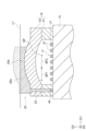
図1は、実施形態に係るSAW装置1(弾性波装置の一例)の断面図である。<SAW device>
(overall structure)
FIG. 1 is a cross-sectional view of a SAW device 1 (an example of an elastic wave device) according to an embodiment.
SAW装置1は、例えば、概略、D3方向を厚さ方向とする薄型の直方体状に形成されている。図1は、例えば、その直方体の4つの側面(D3方向に平行な面)のうちのいずれかに平行な断面を示している。SAW装置1の大きさは適宜に設定されてよい。一例を挙げると、平面視における1辺の長さは1mm以上5mm以下であり、厚さは、0.3mm以上1mm以下である。
The
SAW装置1は、例えば、不図示の回路基板等に表面実装される電子部品として構成されている。具体的には、例えば、SAW装置1は、+D3側に面する上面1aから露出している複数の外部端子5を有している。SAW装置1は、例えば、不図示の回路基板に対して上面1aを対向させて配置され、回路基板に設けられたパッドと外部端子5とがはんだ等からなるバンプを介して接合されることにより回路基板に実装される。そして、SAW装置1は、例えば、複数の外部端子5のいずれかを介して電気信号が入力され、入力された電気信号に所定の処理を施して複数の外部端子5の他のいずれかから出力する。
The
図2は、SAW装置1が含むSAWチップ3(以下、単に「チップ3」ということがある。)の断面図であり、図1の一部に相当している。
FIG. 2 is a cross-sectional view of the SAW chip 3 (hereinafter sometimes simply referred to as "
図1および図2に示すように、SAW装置1は、例えば、チップ3と、チップ3をパッケージングしているパッケージ7とを有している。チップ3は、例えば、信号の処理を直接に及び/又は中心的に担う。パッケージ7は、チップ3の保護、及び/又はチップ3と外部(上述した不図示の回路基板)との電気的な仲介に寄与する。
As shown in FIGS. 1 and 2, the
パッケージ7は、チップ3の表面の大部分を覆っている包囲部9と、チップ3及び包囲部9に対して+D3側に重なっている配線層11とを有している。包囲部9は、例えば、主としてチップ3の保護に寄与している。配線層11は、上述した外部端子5を含んでおり、例えば、チップ3と外部との電気的な仲介を担う。もちろん、配線層11は、チップ3の保護に寄与してもよい。
The
図示の例では、SAW装置1は、1つのチップ3のみを有している。特に図示しないが、SAW装置1は、パッケージ7によって共にパッケージングされた複数のSAWチップ3を有していてもよいし、1以上のSAWチップ3と、別の種類のチップ(例えばIC(Integrated Circuit))とを有していてもよい。複数のチップは、例えば、配線層11(D1-D2平面)に沿って並べられる。
In the illustrated example, the
(チップの全体構成)
チップ3は、例えば、基本的に、パッケージ7によってパッケージされなくとも、不図示の回路基板等に対して表面実装可能なWLP型のSAWチップと同様の構成とされてよい。ただし、チップ3は、パッケージ7によってパッケージされることから、単体で実装されるWLP型のSAWチップと異なる構成(構造、寸法及び/又は材料)を有していてもよい。例えば、強度確保のための部材が薄くされたり、外部との接合のための導体が小さくされたりしてもよい。(Overall configuration of chip)
For example, the
チップ3は、例えば、概略、D3方向を厚さ方向とする薄型の直方体状に形成されている。図1及び図2は、例えば、その直方体の4つの側面(D3方向に平行な面)のいずれかに平行な断面を示している。チップ3は、例えば、+D3側に面する上面19aから露出している複数のチップ端子13を有している。チップ3は、例えば、複数のチップ端子13のいずれかを介して電気信号が入力され、入力された電気信号に所定の処理を施して複数のチップ端子13の他のいずれかから出力する。
The
チップ3は、基板15と、基板15の第1主面15aに位置している励振電極17と、励振電極17の上から第1主面15aを覆っているカバー19とを有している。励振電極17によって基板15に電圧が印加されることによって第1主面15aが振動し、ひいては、SAWが励振される。このSAWを利用して、例えば、チップ3に入力された信号に対する処理がなされる。カバー19は、例えば、励振電極17上に空間SPを構成することによって、第1主面15aの振動を容易化することに寄与している。
The
また、チップ3は、例えば、第1主面15a上に位置している第1導体層21、カバー19をD3方向に貫通している複数の第1貫通導体23、カバー19の上面19a上に位置している第2導体層25を有している。第1導体層21は、例えば、励振電極17を含んでいる。第2導体層25は、例えば、チップ端子13を含んでいる。複数の第1貫通導体23は、例えば、第1導体層21と第2導体層25との導通に寄与している。特に図示しないが、チップ3は、この他、カバー19内に位置し(カバー19に埋設され)、第1主面15aに平行な導体層を有していてもよい。
The
チップ3は、上記の他、不図示の種々の構成を備えていて構わない。例えば、チップ3は、第1導体層21の大部分(例えば励振電極17)を覆う絶縁性の保護膜(例えばSiO2膜)を有していてもよい。保護膜は、比較的薄い、単に第1導体層21を腐食等から保護する目的のものであってもよいし、比較的厚い、チップ3の温度補償に寄与するものであってもよい。また、例えば、基板15の-D3側の面(第2主面15b)を覆う裏面電極が設けられていてもよいし、当該裏面電極を覆う絶縁膜が設けられていてもよい。また、例えば、基板15の側面(D3軸に沿う面)及び/又はカバー19の側面(D3軸に沿う面)を覆う絶縁膜が設けられていてもよい。また、例えば、第2導体層25の一部の領域を覆う絶縁膜が設けられていてもよい。The
(基板)
基板15の形状は適宜に設定されてよい。例えば、基板15の形状は、概略、D3方向を厚さ方向とする薄型の直方体状である。図1及び図2は、例えば、その直方体の4つの側面(D3方向に平行な面)のいずれかに平行な断面を示している。基板15は、少なくとも第1主面15aのうちの励振電極17が配置されている所定領域15aaにおいて圧電性を有している。(substrate)
The shape of the
所定領域15aaに圧電性を有している基板15としては、例えば、基板全体が圧電体によって構成されているもの(すなわち圧電基板)を挙げることができる。また、例えば、いわゆる貼り合わせ基板を挙げることができる。貼り合わせ基板は、第1主面15aを有する圧電体からなる基板(圧電基板)と、この圧電基板の第1主面15aとは反対側の面に、接着剤を介して、又は接着剤を介さずに直接に貼り合わされた支持基板とを有している。また、所定領域15aaに圧電性を有している基板15としては、例えば、支持基板と、支持基板の+D3側の主面の一部領域又は主面の全面に、圧電体からなる膜(圧電膜)又は圧電膜を含む多層膜が形成されたものを挙げることができる。
As the
基板15のうちの少なくとも所定領域15aaを構成している圧電体は、例えば、圧電性を有する単結晶によって構成されている。このような単結晶を構成する材料としては、例えば、タンタル酸リチウム(LiTaO3)、ニオブ酸リチウム(LiNbO3)及び水晶(SiO2)を挙げることができる。カット角、平面形状および各種の寸法は適宜に設定されてよい。The piezoelectric material forming at least the predetermined region 15aa of the
基板15は、図示の例とは異なり、第1主面15aに段差を有していてもよい。例えば、上記のように支持基板の主面上に圧電膜が形成される態様において、第1主面15aのうちの圧電膜によって構成される領域は、第1主面15aのうちの支持基板の主面によって構成される領域よりも高くなっていてよい。また、基板15は、図示の例とは異なり、側面に突部を有していたり、-D3側ほど基板15が広くなる、又は狭くなる向きで側面が傾斜していたりしてよい。
Unlike the illustrated example, the
(励振電極及びその周辺の導体)
図3は、励振電極17を説明するための模式的な平面図である。この図は、励振電極17の上から基板15の所定領域15aaの一部を見た平面図となっている。(Excitation electrode and surrounding conductor)
FIG. 3 is a schematic plan view for explaining the
図示の例では、励振電極17は、いわゆるIDT(interdigitated transducer)電極によって構成されている。また、図示の例では、励振電極17は、1対の反射器29と組み合わされることにより、いわゆる1ポートSAW共振子27を構成している。SAW共振子27は、例えば、模式的に示された2つのチップ端子13の一方から所定の周波数の電気信号が入力されると共振を生じ、その共振を生じた信号を2つのチップ端子13の他方から出力する。図3では、励振電極17に接続される配線31も図示されている。
In the illustrated example, the
励振電極17、反射器29及び配線31は、第1主面15a上の既述の第1導体層21を構成している。第1導体層21の材料については後述する。励振電極17及び反射器29等の厚さは、SAWチップ3に要求される電気特性等に応じて適宜に設定されてよい。特に図示しないが、励振電極17及び/又は反射器29の上面または下面には、SAWの反射係数を向上させるために、絶縁体または金属からなる付加膜が設けられていてもよい。
The
励振電極17は、1対の櫛歯電極33を有している。なお、図3では、視認性をよくする便宜上、1対の櫛歯電極33の一方及び当該一方に接続されている配線31にハッチングを付している。各櫛歯電極33は、例えば、バスバー35と、バスバー35から互いに並列に延びる複数の電極指37と、複数の電極指37の間においてバスバー35から突出する複数のダミー電極39とを有している。そして、1対の櫛歯電極33は、複数の電極指37が互いに噛み合うように(交差するように)配置されている。図1及び図2の断面図においては、励振電極17のうち電極指37が模式的に示されている。
The
1対の櫛歯電極33に電圧が印加されると、電極指37によって所定領域15aaに電圧が印加され、D1軸方向に伝搬する所定のモードのSAWが励起される。励起されたSAWは、電極指37によって機械的に反射される。その結果、電極指37のピッチを半波長とする定在波が形成される。反射器29は、この定在波を構成するSAWの漏れを低減する。定在波は、当該定在波と同一周波数の電気信号に変換され、電極指37によって取り出される。このようにしてSAW共振子27は共振子として機能する。その共振周波数は、電極指ピッチを半波長として所定領域15aaを伝搬するSAWの周波数と概ね同一の周波数である。
When a voltage is applied to the pair of comb-
図3は、励振電極17の構成の一例を模式的に示しているに過ぎず、励振電極17の具体的な構成は適宜に設定及び/又は変形されてよい。例えば、電極指37の数及び各種の寸法等は適宜に設定されてよい。電極指37のピッチは、一定であってもよいし、微小な量で変動してもよいし、特異なピッチ(例えば狭ピッチ部)が一部に存在してもよい。複数の電極指37を接続しているバスバー(符号省略)は、図示の例のようにD1方向に平行であってもよいし、図示の例とは異なり、D1方向に傾斜していてもよい。励振電極17は、ダミー電極39を有していなくてもよい。隣り合う2本の電極指の先端同士のD2方向における距離(いわゆる交差幅)は、図示の例のように一定であってもよいし、図示の例とは異なり、D1方向の位置によって異なっていてもよい(いわゆるアポダイズが施されていてもよい。)。少数の電極指37が実質的に間引かれた部分が存在してもよい。
FIG. 3 only schematically shows an example of the configuration of the
後述するように、チップ3は、互いに接続された複数のSAW共振子27によって構成されたラダー型フィルタを有していてもよい。また、励振電極17は、SAW共振子27を構成するのではなく、1対の反射器29の間にD1軸方向に複数で配列されることによって、多重モード型(本開示においてはダブルモード型を含むものとする。)共振子フィルタを構成してもよい。
As will be described later, the
(カバー)
図1及び図2に戻って、カバー19の外形(空間SP等を無視した形状)は適宜に設定されてよい。例えば、カバー19の外形は、概略、D3方向を厚さ方向とする薄型の直方体状である。図1及び図2は、例えば、その直方体の4つの側面(D3方向に平行な面)のいずれかに平行な断面を示している。また、カバー19は、例えば、平面視において基板15の第1主面15aよりも一回り小さく、カバー19の全周に亘って第1主面15aの外縁部を露出させている。(cover)
Returning to FIGS. 1 and 2, the outer shape of the cover 19 (the shape ignoring the space SP, etc.) may be set as appropriate. For example, the outer shape of the
カバー19は、例えば、平面視において枠状の枠部41と、枠部41の開口を塞ぐ蓋部43とを有している。枠部41の開口が蓋部43によって塞がれることにより、密閉された空間SPが構成されている。空間SP内は、例えば、真空状態(厳密には減圧された状態)とされていてもよいし、適宜な気体(例えば窒素)が封入されていてもよい。気体が封入されている場合、その気圧は、大気圧に対して、低くてもよいし、同程度であってもよいし、高くてもよい。
The
枠部41は、例えば、概ね一定の厚さの層に空間SPとなる開口が1以上形成されることにより構成されている。枠部41のD3方向の厚さ(空間SPの高さ)は、例えば、5μm以上30μm以下である。蓋部43は、例えば、枠部41上に積層される、概ね一定の厚さの層により構成されている。蓋部43の厚さ(D3方向)は、例えば、5μm以上30μm以下である。枠部41の厚さと蓋部43の厚さとは、互いに同一であってもよいし、互いに異なっていてもよい。平面視における枠部41の厚さ(D1方向又はD3方向。壁の厚さ)は、任意に設定されてよい。
The
枠部41および蓋部43は、同一の材料により形成されていてもよいし、互いに異なる材料により形成されていてもよい。図1及び図2では、説明の便宜上、枠部41と蓋部43との境界線を明示しているが、現実の製品においては、枠部41と蓋部43とは、同一材料により一体的に形成されていてもよい。また、枠部41および蓋部43それぞれは、複数層から構成されていてもよい。
The
カバー19(枠部41および蓋部43)は、基本的に絶縁材料によって構成されている。絶縁材料は、例えば、感光性の樹脂である。感光性の樹脂は、例えば、アクリル基やメタクリル基などのラジカル重合により硬化する樹脂である。このような樹脂としては、ウレタンアクリレート系、ポリエステルアクリレート系、エポキシアクリレート系のものを挙げることができる。
The cover 19 (
(チップにおける種々の導体)
第1導体層21は、例えば、既述のように、励振電極17、反射器29及び配線31を有している。また、第1導体層21は、例えば、励振電極17と配線31を介して接続されている内部端子45を有している。内部端子45は、例えば、第1貫通導体23と直接的に接続される部分である。この他、第1導体層21は、例えば、インダクタ及び/又はキャパシタ等の電子素子を構成するパターンを有していてもよい。(Various conductors in chips)
The
第1導体層21が含む種々の部位は、材料及び厚さが互いに同一であってもよいし、材料及び/又は厚さが互いに異なっていてもよい。また、第1導体層21の種々の部位は、1層の金属層から構成されていてもよいし、互いに異なる材料からなる複数の金属層から構成されていてもよい。例えば、励振電極17、反射器29及び配線31は、互いに同一の材料及び同一の厚さの第1層によって構成され、内部端子45は、前記の第1層と、その上に重なる第1層とは異なる材料からなる第2層とによって構成されてよい。第1層及び第2層もそれぞれ2以上の金属層から構成されても構わない。第1層の全部、第1層の厚みの8割以上又は第1層の厚みの5割以上を占める材料としては、例えば、Al又はAlを主成分とする合金を挙げることができる。そのような合金としては、例えば、Al-Cu合金を挙げることができる。主成分は、例えば、50質量%以上又は80質量%以上を占める成分である(以下、同様。)。
The various parts included in the
内部端子45の数は、励振電極17によって構成される回路の構成等に応じて適宜に設定されてよい。内部端子45の形状及び寸法も適宜に設定されてよい。例えば、内部端子45の平面形状は円形とされてよい。また、内部端子45と配線31との境界は明瞭でなくてよい。内部端子45の位置も適宜に設定されてよい。例えば、内部端子45は、基板15の第1主面15aの外周縁に隣接する位置(例えば外周縁との最短距離が内部端子45の径以下の位置)に設けられていてもよいし、前記の位置よりも離れた位置に設けられていてもよい。
The number of
第1貫通導体23は、例えば、カバー19の厚みの少なくとも一部を貫通する柱状に形成されており、内部端子45及び第2導体層25の少なくとも一方に直接に接続されて、両者の電気的な接続に寄与している。図示の例では、第1貫通導体23は、カバー19の実質的に全厚み(枠部41及び蓋部43)を貫通して、内部端子45と第2導体層25との双方に直接に接続されている。図示の例以外の態様としては、特に図示しないが、例えば、枠部41を貫通して内部端子45に接続される第1貫通導体23と、蓋部43を貫通して第2導体層25に接続される第1貫通導体23とが設けられ、両者が枠部41と蓋部43との間の導体層によって接続される態様を挙げることができる。
The first penetrating
第1貫通導体23の具体的な形状及び寸法は適宜に設定されてよい。例えば、第1貫通導体23の第1主面15aに平行な断面の形状は円形又は楕円形とされてよい。また、例えば、第1貫通導体23は、貫通方向において径が一定であってもよいし、一定でなくてもよい。後者としては、例えば、テーパ形状、逆テーパ形状、及び/又は枠部41を貫通する部分と蓋部43を貫通する部分とで径が異なる形状を挙げることができる。また、複数の第1貫通導体23の形状、寸法及び/又は材料は、互いに同一であってもよいし、互いに異なっていてもよい。
The specific shape and dimensions of the first through
第1貫通導体23の材料は、適宜な金属とされてよい。また、第1貫通導体23は、その全体が同一の材料によって構成されていてもよいし、一部同士が互いに異なる材料によって構成されていてもよい。後者としては、例えば、第1貫通導体23が、カバー19の孔の内面に成膜されている下地層と、下地層の内側に電気めっき等によって形成された本体部とを有している構成を挙げることができる。なお、この場合、本体部のみを第1貫通導体23として捉えても構わない。第1貫通導体23の材料は、第1導体層21の材料と同一であってもよいし、異なっていてもよい。後者の場合の材料としては、例えば、音響的な観点も踏まえて選択された第1導体層21の要部(例えば励振電極17)の材料よりも導電性が高い(電気抵抗率が低い)材料を挙げることができる。例えば、上記のように第1導体層21の材料がAl又はAlを主成分とする合金の場合において、第1貫通導体23の材料は、Cu又はCuを主成分とする合金とされてよい。
The material of the first through
第2導体層25は、例えば、既述のように、チップ端子13を有している。また、第2導体層25は、例えば、第1貫通導体23とチップ端子13とを接続する配線(符号省略)、及び適宜な導体パターン47を有している。
The
チップ端子13は、例えば、第1貫通導体23及び内部端子45を介して励振電極17と電気的に接続されている。チップ端子13の数は、チップ3における回路の構成等に応じて適宜に設定されてよい。チップ端子13の数は、内部端子45の数と同一であってもよいし、異なっていてもよい。チップ端子13の形状及び寸法も適宜に設定されてよい。例えば、チップ端子13の平面形状は円形とされてよい。また、チップ端子13と第2導体層25が含む配線との境界は明瞭でなくてよい。
The
チップ端子13のカバー19の上面19a内における位置は適宜に設定されてよい。例えば、チップ端子13は、平面透視において、内部端子45及び/又は第1貫通導体23の全部に重なっていてもよいし、内部端子45及び/又は第1貫通導体23の一部又は全部に重なっていなくてもよい。また、例えば、チップ端子13は、平面透視において、一部又は全部が空間SPの一部に重なっていてもよいし、全部が空間SPに重なっていなくてもよい。
The position of the
チップ端子13と内部端子45との具体的な接続態様は適宜に設定されてよい。例えば、チップ端子13は、直下に位置する第1貫通導体23に直接に接続されることによって直下の内部端子45に電気的に接続されてよい。また、チップ端子13は、第2導体層25が含む不図示の配線等によって直下にない第1貫通導体23と電気的に接続されることによって、直下にない内部端子45と電気的に接続されていてもよい。また、チップ端子13は、カバー19内に埋設されている不図示の導体層を介して、直下にない内部端子45と電気的に接続されていてもよい。
The specific manner of connection between the
導体パターン47としては、例えば、蓋部43を補強することに寄与する補強層を挙げることができる。補強層の平面視における形状及び寸法は適宜に設定されてよい。例えば、補強層は、平面透視において、空間SPの全体を覆っていてもよいし、空間SPの一部を覆っていてもよいし、空間SPの内外に跨っていてもよい。また、補強層は、例えば、電気的に浮遊状態(電位が付与されない状態)とされてもよいし、基準電位が付与されてもよい。また、補強層は、第1貫通導体23と接続されていてもよいし、接続されていなくてもよい。前者の場合においては、補強層は、第1貫通導体23を介して第1主面15aに支持される。
As the
また、導体パターン47としては、例えば、インダクタ及び/又はキャパシタ等の電子素子を構成するパターンを挙げることができる。このような電子素子は、例えば、第1貫通導体23を介して内部端子45と接続されたり、及び/又は第2導体層25が含む不図示の配線を介してチップ端子13と接続されたりしてよい。ひいては、電子素子は、励振電極17と電気的に接続されてよい。
Moreover, as the
第2導体層25が含む種々の部位は、材料及び厚さが互いに同一であってもよいし、材料及び/又は厚さが互いに異なっていてもよい。また、第2導体層25の種々の部位は、1層の金属層から構成されていてもよいし、互いに異なる材料からなる複数の金属層から構成されていてもよい。例えば、第2導体層25は、特に図示しないが、カバー19の上面19a上(第1貫通導体23の直上は除く)に位置する下地層と、当該下地層上に電気めっき等によって形成された本体部とを含んでよい。第2導体層25(全部又は本体部)の材料は、例えば、第1貫通導体23と同様に、第1導体層21の要部(例えば励振電極17)の材料よりも導電性が高い(電気抵抗率が低い)材料とされてよく、具体的には、Cu又はCuを主成分とする合金とされてよい。
The various parts included in the
第2導体層25の材料は、第1貫通導体23の材料と同一であってもよいし、異なっていてもよい。前者としては、例えば、カバー19の第1貫通導体23が配置される孔の内面から上面19aに亘って広がる下地層と、下地層上に析出された金属材料(本体部)とによって第1貫通導体23及び第2導体層25が共に形成されている態様を挙げることができる。
第2導体層25は厚さ方向(D3方向)において拡幅部を備えない。言い換えると、第2導体層25の幅が、厚さ方向の中央付近で最大値となるような幅変化がない。これにより、平面視で隣り合う第2導体層25間の短絡を抑制することができる。また、包囲部9との接合性も高まり、剥離を低減し信頼性を高めることができる。さらに、厚さ方向における幅変化による電気特性の変動を抑制することができる。
また、第2導体層25の厚さは、枠部や蓋部、後述の第1および第2絶縁層の厚さよりも薄い。これにより、チップと配線層との距離を近付けることができる。The material of the
The
Further, the thickness of the
(包囲部)
図1に示す包囲部9は、例えば、チップ3の第2導体層25の上面を除いて、チップ3の全体を覆っている。具体的には、包囲部9は、チップ3の全て(ここでは4つ)の側面の全体を覆っている。すなわち、包囲部9は、基板15の全ての側面を覆っているとともに、カバー19の全ての側面を覆っている。また、包囲部9は、例えば、チップ3の下面(-D3側の面。基板15の第2主面15b)の全体を覆っている。また、包囲部9は、例えば、カバー19の上面19aのうち第2導体層25の非配置領域を覆っている。また、包囲部9は、基板15の第1主面15aのうちカバー19よりも外縁側の部分を覆っている。(Encircling part)
The surrounding
既述のように、1つのSAW装置1は、配線層11に沿って配列された複数のチップ(例えばチップ3)を有していても構わない。この場合、包囲部9は、複数のチップが外部に露出しないように複数のチップ全体を覆う。ただし、包囲部9は、互いに隣り合うチップ3同士の間に隙間なく充填されていてもよいし、チップ3同士の間に、真空状態とされた、又は気体が封入された空間を構成していてもよい。
As described above, one
包囲部9は、基板15の側面及び第2主面15b並びにカバー19の側面等の各種の面に対して直接に密着して当該各種の面を覆っていてもよいし、各種の面に密着する他の部材(層)に密着して間接的に各種の面を覆っていてもよい。例えば、上述のように、チップ3は、第2主面15bに重なる裏面電極及び当該裏面電極を覆う絶縁層が設けられてよく、包囲部9は、この絶縁層に密着することによって第2主面15bを覆っていてもよい。なお、同様に、本開示において、他の部材及び面について、覆う(又は重なる等)という場合、直接的に覆う態様だけでなく、間接的に覆う態様を含むものとする。
The surrounding
包囲部9は、SAW装置1の外形を配線層11とで構成しており、SAW装置1の外形のうちの-D3側の大部分を構成している。SAW装置1の外形となる包囲部9の外形は適宜に設定されてよい。図示の例では、SAW装置1全体の説明から理解されるように、包囲部9の外形は、概略、D3方向を厚さ方向とする薄型の直方体状である。ただし、図示の例とは異なり、例えば、包囲部9は、側面に突部を有していたり、-D3側ほどSAW装置1が広くなる、又は狭くなるように側面が傾斜していたりしてもよい。また、例えば、包囲部9の側面は、基板15及び/又はカバー19の側面と平行であってもよいし(図示の例)、平行でなくてもよい。
The surrounding
包囲部9の各種の寸法は適宜に設定されてよい。例えば、基板15及びカバー19の側面を覆う部分の厚さ(D1方向又はD2方向)及び包囲部9の第2主面15bを覆う部分の厚さ(D3方向)は、同等であってもよいし、互いに大きく異なっていてもよい。また、基板15及びカバー19の4つの側面を覆う部分の厚さは、側面同士で同等であってもよいし、異なっていてもよい。
Various dimensions of the surrounding
包囲部9は、例えば、その全体が同一の材料によって一体的に形成されている。包囲部9の材料は、例えば、絶縁材料とされている。絶縁材料は、有機材料であってもよいし、無機材料であってもよい。例えば、包囲部9は、その全部又は母材が樹脂によって構成されている。樹脂は、例えば、熱硬化性樹脂とされてよい。熱硬化性樹脂としては、例えば、エポキシ樹脂及びフェノール樹脂を挙げることができる。樹脂には、絶縁性粒子からなるフィラーが混入されていてもよい。絶縁性粒子は、例えば、樹脂よりも熱膨張係数が低い材料によって構成されてよい。絶縁性粒子の材料は、例えば、シリカ、アルミナ、フェノール、ポリエチレン、グラスファイバー、グラファイトである。
For example, the entire surrounding
(配線層)
図1に示す配線層11は、カバー19の上面19a、第2導体層25の上面、及び包囲部9の上面を覆っている。平面視において、配線層11は、例えば、上記の3種の面の全部を過不足なく覆う形状及び大きさとされている。換言すれば、平面視において、配線層11の外縁は、包囲部9の外縁に一致している。ただし、図示の例とは異なり、配線層11は、上記の3種の面の一部を露出させていてもよい。例えば、配線層11の外縁の一部又は全部は、包囲部9の外縁よりも内側に位置していてもよい。また、逆に、配線層11の外縁の一部又は全部は、包囲部9の外縁よりも外側に位置していてもよい。(wiring layer)
The
配線層11は、例えば、絶縁基材49と、絶縁基材49に配置された種々の導体とを有している。種々の導体は、例えば、既述の外部端子5を含んでいるとともに、外部端子5とチップ端子13とを接続する第2貫通導体51を含んでいる。この他、特に図示しないが、配線層11の導体は、例えば、絶縁基材49内に位置するD1-D2平面に平行な導体層及び/又は絶縁基材49の上面に重なる導体層を有していてもよい。
The
配線層11等の厚さは適宜に設定されてよい。例えば、比較的薄い場合の例を挙げると、カバー19の上面19aから配線層11の上面(図示の例では外部端子5の上面)若しくは絶縁基材49の上面までの距離は、カバー19の厚さ(枠部41及び蓋部43の合計厚さ。本段落において、以下、同様。)に対して、2倍以下、1.5倍以下又は1倍以下とされてよい。又は、配線層11の厚さ(図示の例では絶縁基材49の下面から外部端子5の上面までの距離)又は絶縁基材49の厚さが、カバー19の厚さの2倍以下、1.5倍以下又は1倍以下とされてもよい。なお、平面視における位置によって上記のようなD3方向の距離又は厚さが異なる場合は、例えば、最大値が比較対象として利用されてよい。
The thickness of the
(絶縁基材)
絶縁基材49は、複数の層によって構成されていてもよいし(図示の例)、1層によって構成されていてもよい。絶縁基材49が複数の層を有している場合、その層の間には不図示の導体層が設けられてよい。絶縁基材49が有している複数の層は、互いに同一の材料によって構成されていてもよいし、互いに異なる材料から構成されていてもよい。絶縁基材49の厚さ及び絶縁基材49を構成する複数の層それぞれの厚さは、チップ3の保護及び/又は絶縁等の観点から適宜に設定されてよい。絶縁基材49の材料は、樹脂等の有機材料であってもよいし、SiO2等の無機材料であってもよいし、無機材料からなるフィラーが混入された樹脂のように、有機材料と無機材料とが混合されたものであってもよい。(Insulating base material)
The insulating
図示の例では、絶縁基材49は、チップ3及び包囲部9の上面に重なる第1絶縁層53と、第1絶縁層53に重なる第2絶縁層55とを有している。第1絶縁層53及び第2絶縁層55は、互いに異なる材料によって構成されてよい。例えば、第1絶縁層53の材料は、エポキシ系の樹脂とされ、第2絶縁層55の材料は、ポリイミド系の樹脂とされてよい。この場合、例えば、第1絶縁層53の加工が容易である一方で、第2絶縁層55によって絶縁基材49の耐熱性を向上させることができる。
In the illustrated example, the insulating
なお、第1絶縁層53,第2絶縁層55の厚さは、第2導体層25の厚さよりも厚い。すなわち、第2導体層25を薄くして、厚さ方向における距離を短くして電気的なロスを小さくすることができる。
Note that the first insulating
(外部端子)
外部端子5は、+D3側に露出する上面を有している。このような外部端子5は、絶縁基材49の上面に形成された導体層によって構成されていてもよいし、絶縁基材49の内部に形成され、絶縁基材49に形成された穴から+D3側に露出する導体層及び/又は貫通導体によって構成されていてもよい。図示の例では、外部端子5は、第1絶縁層53の上面に形成された導体層によって構成されており、第2絶縁層55に形成された孔(符号省略)から+D3側に露出している。より詳細には、外部端子5の-D3側の一部(後述する第3導体層57の外周部)は、第2絶縁層55に覆われている。(external terminal)
The
外部端子5は、その全体が単一の材料によって構成されていてもよいし、互いに異なる材料からなる複数の部位の組み合わせによって構成されていてもよい。図示の例では、外部端子5は、第1絶縁層53の上面に重なる第3導体層57と、第3導体層57に重なる第4導体層59とを有している。第3導体層57及び第4導体層59は、例えば、互いに異なる材料によって構成されている。
The entire
第3導体層57は、1層の金属層によって構成されていてもよいし、複数層の金属層によって構成されていてもよい。後者としては、例えば、特に図示しないが、第1絶縁層53の上面上(第2貫通導体51の直上は除く)に位置する下地層と、当該下地層上に電気めっき等によって形成された本体部とを有するものを挙げることができる。第3導体層57(全部又は本体部)の材料は、例えば、第2導体層25と同様に、第1導体層21の要部(例えば励振電極17)の材料よりも導電性が高い(電気抵抗率が低い)材料とされてよく、具体的には、Cu又はCuを主成分とする合金とされてよい。
The
第4導体層59は、1層の金属層によって構成されていてもよいし、複数層の金属層によって構成されていてもよい。第4導体層59の材料には、例えば、いわゆるバリアメタルに利用される材料が用いられてよい。例えば、Cr、Au、Ti及び/又はNiが用いられてよい。このような材料が用いられることにより、例えば、接合強度の向上及び/又は意図されていない金属間化合物の生成の低減が図られる。
The
平面視における外部端子5の位置は適宜に設定されてよい。例えば、外部端子5は、平面透視において、チップ3内に収まっていてもよいし、一部又は全部がチップ3の外部に位置していてもよい。換言すれば、外部端子5は、平面透視において、包囲部9に重なっていなくてもよいし、一部又は全部が包囲部9に重なっていてもよい。また、例えば、複数の外部端子5は、上面1aの外周縁に沿って配列されているものを含んでよい。この場合において、外部端子5と上面1aの外周縁との最短距離は、例えば、外部端子5の径以下とされてよい。また、このような位置よりも外周縁から離れた外部端子5が設けられても構わない。また、例えば、外部端子5は、平面透視において、第2貫通導体51及び/又はチップ端子13の全部に重なっていてもよいし、これらの一部又は全部に重なっていなくてもよい。また、例えば、外部端子5は、平面透視において、一部又は全部が空間SPの一部に重なっていてもよいし、全部が空間SPに重なっていなくてもよい。
The position of the
外部端子5の数は、SAW装置1が有している回路構成に応じて適宜に設定されてよい。外部端子5の数は、チップ端子13の数と同一であってもよいし、異なっていてもよい。外部端子5の平面形状及び寸法も適宜に設定されてよい。例えば、チップ端子13の平面形状は円形とされてよい。
The number of
(第2貫通導体)
第2貫通導体51は、例えば、絶縁基材49の厚みの少なくとも一部を貫通する柱状に形成されており、チップ端子13及び外部端子5の少なくとも一方に直接に接続されて、両者の電気的な接続に寄与している。図示の例では、第2貫通導体51は、第1絶縁層53を貫通して、チップ端子13と外部端子5との双方に直接に接続されている。図示の例以外の態様については、後に例示する(図10(b))。(Second through conductor)
The second penetrating
第2貫通導体51の具体的な形状及び寸法は適宜に設定されてよい。例えば、第2貫通導体51の上面1aに平行な断面の形状は円形又は楕円形とされてよい。また、例えば、第2貫通導体51は、貫通方向において径が一定であってもよいし、一定でなくてもよい。後者としては、例えば、テーパ形状、逆テーパ形状、及び/又は複数の絶縁層を貫通する複数の部位同士で径が異なる形状を挙げることができる。また、複数の第2貫通導体51の形状、寸法及び/又は材料は、互いに同一であってもよいし、互いに異なっていてもよい。
The specific shape and dimensions of the second through
第2貫通導体51の材料は、適宜な金属とされてよい。また、第2貫通導体51は、その全体が同一の材料によって構成されていてもよいし、一部同士が互いに異なる材料によって構成されていてもよい。後者としては、例えば、第2貫通導体51が、第1絶縁層53の孔の内面に成膜されている下地層と、下地層の内側に電気めっき等によって形成された本体部とを有している構成を挙げることができる。なお、この場合、本体部のみを第2貫通導体51として捉えても構わない。第2貫通導体51の材料は、第2導体層25及び/又は第3導体層57の材料と同一であってもよいし、異なっていてもよい。また、第2貫通導体51の材料は、例えば、第3導体層57等と同様に、第1導体層21の要部(例えば励振電極17)の材料よりも導電性が高い(電気抵抗率が低い)材料とされてよく、具体的には、Cu又はCuを主成分とする合金とされてよい。
The material of the second through
(カバー上面から外部端子までの導体の材料)
これまでの説明から理解されるように、チップ端子13と、配線層11の導体(より詳細には第2貫通導体51)とは、直接的に接続されている。従って、両者の間には、はんだ等の低融点金属からなる接合部材は介在していない。なお、直接的な接続は、両者が接合されている状態であってもよいし、単に当接しているだけの状態であってもよい。低融点金属は、例えば、融点が450℃未満の金属である。JIS(日本工業規格) Z 3001-3では、はんだは、融点が450℃未満の材料として定義されている。(Material of the conductor from the top of the cover to the external terminal)
As understood from the above description, the
上記について別の表現をする。励振電極17と外部端子5とを接続している導体(例えば、配線31、内部端子45、第1貫通導体23、チップ端子13及び第2貫通導体51)を接続導体61と呼称するものとする。接続導体61のうち、カバー19の上面19aよりも基板15側の位置から外部端子5に至る部分(例えば第1貫通導体23の少なくとも+D3側の部分、チップ端子13及び第2貫通導体51)を第1部分61aと呼称するものとする。このとき、第1部分61aは、融点が450℃以上の材料によって構成されている。すなわち、融点が450℃以上の材料がカバー19の上面19aよりも下方から外部端子5まで連続している。
Let me express the above in another way. The conductor connecting the
ここで、材料の融点を確認するためには、例えば分解したり、樹脂包埋後に断面出しを行なったりすることで、当該部分を露出させて組成分析を行ない、相図から判定することができる。また、分解後に加熱することで目視により確認することができる。さらに、当該部分を取り出し、融点測定装置で分析してもよい。 Here, in order to confirm the melting point of a material, for example, by disassembling it or taking a cross section after embedding it in resin, the relevant part can be exposed and analyzed for its composition, and it can be determined from the phase diagram. . In addition, it can be visually confirmed by heating after decomposition. Furthermore, the portion may be taken out and analyzed using a melting point measuring device.
第1部分61aは、その全体(既述のように下地層は無視されても構わない。)が同一の材料によって形成されていてもよいし、互いに異なる材料によって形成されていてもよい。いずれにせよ、その材料は、例えば、既述のように、音響的な観点も踏まえて選択された励振電極17の材料よりも導電性が高い(電気抵抗率が低い)材料とされてよく、具体的には、Cu又はCuを主成分とする合金とされてよい。
The
(第2導体層の厚さの詳細)
図4は、チップ3の一部を模式的に示す断面図である。(Details of thickness of second conductor layer)
FIG. 4 is a cross-sectional view schematically showing a part of the
蓋部43は、例えば、少なくとも空間SP上において空間SPとは反対側(+D3側)へ撓んでいる(湾曲している)。別の観点では、空間SPは、基板15からの高さが互いに異なる部分を有している。また、蓋部43の湾曲に伴い、蓋部43上に位置している第2導体層25の下面は、+D3側へ湾曲している。一方、第2導体層25の上面は、直線LPで示されているように、平面状となっている。別の観点では、第2導体層25は、互いに厚さが異なる領域を有している。ここでいう平面状は、例えば、第2導体層25の下面の湾曲に比較しての相対的なものであってよく、厳密に平面でなくてもよい。
For example, the
なお、図4では、蓋部43の湾曲、第2導体層25の湾曲及び第2導体層25の厚さの相違等が誇張されて示されている。また、図4では、第2導体層25の厚さが一定であると仮定した場合の第2導体層25の上面側部分が点線で示されている。
In addition, in FIG. 4, the curvature of the
上記の蓋部43の湾曲等について、別の表現をする。空間SPは、基板15の法線方向(D3方向)に見たときに、空間SP1の一部である第1空間部SP1と、他の一部である第2空間部SP2とを有している。第2空間部SP2の基板15からカバー19(蓋部43)までの高さ(D3方向)は、第1空間部SP1のものよりも高い。一方、第2導体層25は、D3方向に透視したときに、第1空間部SP1に重なっている第1領域部25aと、第2空間部SP2に重なっている第2領域部25bとを有している。第2領域部25bは、第1領域部25aよりも薄い。
The above-mentioned curvature of the
第1領域部25aと第2領域部25bとの厚さの差は、適宜に設定されてよい。例えば、第2導体層25において、最も厚い部分の厚さと最も薄い部分との厚さの差は、最も厚い部分の厚さの1/10以上、1/5以上又は1/3以上であり、また、2/3以下又は1/3以下であり、前記の下限と上限とは、矛盾しない限り、適宜に組み合わされてよい。
The difference in thickness between the
(寸法の一例)
以下に、各種の部材の寸法の一例を挙げる。ここで例示する寸法は、あくまで一例であって、実際の寸法は、以下に示す範囲よりも大きく、又は小さくされても構わない。(Example of dimensions)
Examples of dimensions of various members are listed below. The dimensions illustrated here are just examples, and the actual dimensions may be larger or smaller than the range shown below.
枠部41のD3方向の厚み(別の観点では空間SPの最小高さ)及び蓋部43の厚み(D3方向)それぞれは、既述のように、5μm以上30μm以下とされてよく、また、20μm以下とされてよい。枠部41の平面視における厚さ(D1方向又はD2方向等)は、最も薄い部分において、5μm以上30μm以下とされてよく、また、20μm以下とされてよい。第2導体層25の厚さ、別の観点では、カバー19から配線層11(第1絶縁層53)までの距離は、最小値及び/又は最大値が、10μm以上20μm以下とされてよい。絶縁基材49又は第1絶縁層53の厚さは、10μm以上30μm以下とされてよい。第2貫通導体51の径(円形でない場合は最大径)は、15μm以上20μm以下とされてよい。カバー19の上面19aから絶縁基材49の上面までの距離は、20μm以上とされてよく、また、50μm以下又は40μm以下とされてよい。
The thickness of the
(SAW装置の製造方法)
図5は、SAW装置1の製造方法の手順の一例を示すフローチャートである。図6(a)~図6(e)は、図5を補足する断面図である。製造工程は、図6(a)から図6(e)へ順に進む。(Manufacturing method of SAW device)
FIG. 5 is a flowchart showing an example of a procedure for manufacturing the
ステップST1では、チップ3を作製する。チップ3の作製方法は、例えば、一部(後述するステップST1a)を除いて、概略、公知のSAWチップの作製方法と同様とされてよい。
In step ST1, a
例えば、特に図示しないが、まず、基板15が多数個取りされるウェハを準備する。このウェハに対して金属材料の成膜及びパターニングによって第1導体層21を形成する。その上に熱硬化性樹脂からなる樹脂層の形成及びパターニングによって枠部41を形成する。その上に熱硬化性樹脂からなるフィルムを重ねてパターニングすることによって蓋部43を形成する。その後、下地層の形成、電気めっきによる金属材料の析出及びパターニングによって、第1貫通導体23及び第2導体層25を形成する。その後、ウェハがダイシングされることによって、個片化されたチップ3が作製される。
For example, although not particularly shown, a wafer from which a large number of
蓋部43(及び枠部41)は、適宜な時期において加熱されることによって硬化される。このとき、空間SP内の気体が膨張し、ひいては、図4に示したように蓋部43が上方に湾曲することがある。一方、第2導体層25は、例えば、一定の厚さでカバー19上に形成される。その結果、図4において点線で示すように、第2導体層25も上方へ湾曲する。そこで、ステップST1内のステップST1aでは、図4において線L1で示すように、第2導体層25の上面を平坦化する。平坦化は、例えば、研磨によってなされてよい。より詳細には、例えば、半導体製造装置においてウェハの研磨に用いられるCMP(Chemical Mechanical Polishing)装置によって、ダイシング前のチップ3の上面が研磨されてよい。第2導体層25は、研磨されることによって設計値に近くなるように、研磨前においては比較的厚く形成されてよい。
The lid portion 43 (and frame portion 41) is heated and hardened at an appropriate time. At this time, the gas in the space SP expands, and as a result, the
ステップST2では、包囲部9を作製する。
In step ST2, the surrounding
具体的には、まず、図6(a)に示すように、支持体71を準備する。支持体71は、例えば、平坦な上面を有する部材であり、例えば、基板状である。支持体71は、例えば、特に図示しないが、樹脂シートに粘着剤が塗布されて構成され、不図示の支持具に支持される。あるいは、支持体71は、不図示の支持具の平坦な上面に接着材若しくは粘着材が塗布されて形成されていてもよい。
Specifically, first, as shown in FIG. 6(a), a
次に、支持体71上に複数のチップ3を配置する。チップ3は、例えば、カバー19側を支持体71側(下側)にして配置される。図6(a)では不図示であるが、第2導体層25の上面(+D3側の面)は、支持体71に密着している。
Next, a plurality of
次に、図6(b)に示すように、包囲部9となる未硬化状態の材料73を支持体71上に供給して硬化させる。これにより、側面が形成される前の状態の包囲部9が作製される。別の観点では、複数のチップ3と材料73とを含むウェハ75が構成される。
Next, as shown in FIG. 6(b), an
材料73の供給方法は適宜なものとされてよい。例えば、ディスペンサやスクリーン印刷によって液状の材料73が供給されてもよいし、加熱により液状の材料73になるシート状成形体が配置されてもよい。また、材料73の供給は、真空印刷のように、真空状態(厳密には減圧された状態)で行われてよい。この場合、例えば、気泡が形成される蓋然性が低減される。また、例えば、第2導体層25の非配置領域における支持体71とカバー19との隙間に材料73が流れ込みやすくなる。
The
材料73の硬化は、例えば、加圧を行いつつ材料73を加熱することによってなされる。その具体的方法は適宜なものとされてよい。例えば、支持体71を支持する不図示の支持具のヒータによって加熱したり、及び/又は上方からヒータを有する型によって材料73を押圧したりしてよい。
The
その後、図6(c)に示すように、支持体71がウェハ75から除去される。支持体71の除去は、剥離によるものであってもよいし、支持体71を溶融させたり、薬液に溶かしたりすることによって除去するものであってもよい。また、支持体71が除去された面は、適宜に洗浄及び/又は研削若しくは研磨が行われてもよい。
Thereafter, the
ステップST3では、配線層11を設ける。具体的には、図6(d)に示すように、ウェハ75の、支持体71が除去された面に、配線層11が設けられる。配線層11の形成には、例えば、半導体装置における再配線と同様に、アディティブ法又はセミアディティブ法等の公知の方法が用いられてよい。また、配線層11は、フレキシブル基板がウェハ75に貼り合わされることによって設けられてもよい。例えば、フレキシブル基板の主面に位置するパッドをチップ端子13に当接させた状態で、フレキシブル基板をウェハ75に向けて加圧しつつ加熱し、フレキシブル基板の主面の絶縁体(接着層)とカバー19の上面19aとを接着させてよい。
In step ST3, a
ステップST4では、図6(e)に示すように、ウェハ75をダイシングして個片化する。これにより、個片化されたSAW装置1が作製される。ダイシングは、公知の方法によって行われてよく、例えば、ダイシングブレードによって行われてもよいし、レーザによって行われてもよい。配線層11及び包囲部9は、厳密には、このステップで側面が形成されて完成する。
In step ST4, as shown in FIG. 6(e), the
以上のとおり、本実施形態では、弾性波装置(SAW装置1)は、基板15と、励振電極17と、カバー19と、包囲部9と、配線層11と、接続導体61とを有している。基板15は、当該基板15の法線方向(D3方向)の一方側(+D3側)に面している第1主面15aに圧電性の所定領域15aaを有している。励振電極17は、所定領域15aaに位置している。カバー19は、+D3側から励振電極17及び第1主面15aを覆っている。包囲部9は、基板15の側面及びカバー19の側面を覆っており、絶縁性を有している。配線層11は、+D3側に露出している外部端子5を含んでおり、+D3側からカバー19及び包囲部9に重なっている。接続導体61は、励振電極17と外部端子5とを接続している。接続導体61は、カバー19の+D側の面(上面19a)よりも基板15側(-D3側)の位置から外部端子5に至る第1部分61a(第1貫通導体23、チップ端子13及び第2貫通導体51)を含んでいる。第1部分61aの融点は450℃以上である。
As described above, in this embodiment, the acoustic wave device (SAW device 1) includes the
従って、例えば、チップ3をリジッド式の回路基板に実装した後、チップ3を樹脂封止したSAW装置と比較すると、チップ3と回路基板(本実施形態では配線層11)との間に実装のためのはんだ(低融点金属)が設けられなくてよい。その結果、例えば、温度変化に起因する応力が低減され、チップ3と配線層11との接続の信頼性が向上する。また、例えば、はんだがチップ3と配線層11との間に介在している態様に比較して、信号の損失を低減することができる。また、例えば、はんだの厚みが不要であることから低背化に有利である。はんだとの接合性を向上させるために、チップ端子13に広い面積を確保したり、チップ端子13にバリアメタルを設けたりする必要性が低減され、小型化及び簡素化に有利である。
Therefore, for example, compared to a SAW device in which the
別の観点では、本実施形態では、弾性波装置(SAW装置1)の製造方法は、チップ作製ステップ(ST1)と、包囲部作製ステップ(ST2)と、配線層配置ステップ(ST3)とを有している。SAW装置1は、チップ3と、包囲部9と、配線層11とを有している。チップ3は、基板15と、励振電極17と、カバー19とを有している。基板15は、当該基板15の法線方向(D3方向)の一方側(+D3側)に面している第1主面15aに圧電性の所定領域15aaを有している。励振電極17は、所定領域15aaに位置している。カバー19は、+D3側から励振電極17及び第1主面15aを覆っている。包囲部9は、基板15の側面及びカバー19の側面を覆っているとともに、絶縁性を有している。配線層11は、外部端子5を有している。外部端子5は、励振電極17に電気的に接続されており、+D3側に露出している。また、配線層11は、+D3側からカバー19及び包囲部9に重なっている。チップ作製ステップでは、チップ3を作製する。包囲部作製ステップでは、チップ作製ステップの後、未硬化状態の絶縁性材料73をチップ3の周囲に配置して材料73を硬化させ、包囲部9を作製する。配線層配置ステップでは、包囲部作製ステップの後、カバー19及び包囲部9の+D3側に配線層11を設ける。
From another point of view, in this embodiment, the method for manufacturing an acoustic wave device (SAW device 1) includes a chip manufacturing step (ST1), a surrounding part manufacturing step (ST2), and a wiring layer arrangement step (ST3). are doing. The
従って、例えば、本実施形態に係るSAW装置1を実現でき、上述した種々の効果を奏することができる。
Therefore, for example, the
また、例えば、チップ3をリジッド式の回路基板に実装した後、チップ3を樹脂封止する場合においては、チップ3の実装において第1貫通導体23に荷重が加えられる。この荷重は、カバー19に伝わり、空間SPの密閉性に影響を及ぼす。第1貫通導体23の径及びカバー19の厚さは、このような事情を考慮して設定される。本実施形態では、配線層11が設けられる前に包囲部9によってカバー19が包囲され、チップ3が補強されるとともに、カバー19の密閉性が向上する。従って、例えば、第1貫通導体23の径を小さくしたり、蓋部43の厚さ(D3方向)及び枠部41の平面視における厚さ(D1方向又はD2方向等)を薄くしたりすることが容易化される。包囲部9の形成にトランスファモールドを用いず、真空印刷を用いた場合においては、カバー19に付与される圧力が低減されるから、蓋部43の厚さ及び枠部41の平面視における厚さをより薄くすることがさらに容易化される。第1貫通導体23の径を小さくすることができると、例えば、内部端子45の径も小さくすることができる。その結果、第1主面15a上における導体の配置に係る設計の自由度が向上する。
Further, for example, when the
また、例えば、チップ3を回路基板に実装した後に樹脂封止する態様では、回路基板は予め用意されたリジッド式のものに限定される。本実施形態では、配線層11を設ける前にチップ3が包囲部9によって封止されるから、配線層11を設けるプロセスの自由度が向上する。例えば、既に言及したように、半導体装置における再配線と同様のプロセスが行われてもよいし、フレキシブル基板を貼り合わせるプロセスが行われてもよい。なお、本開示に係る製造方法(包囲部作製ステップの後に配線層配置ステップを行うという特徴)に着目した場合においては、チップ3をはんだによってリジッド式の回路基板に載置して実装することによって配線層11が設けられても構わない。
Further, for example, in a mode in which the
上記のようなプロセスの多様化の結果、例えば、設計の自由度が向上する。例えば、チップ3をリジッド式の回路基板に実装しない場合においては、チップ端子13の位置は、チップ3を安定して回路基板上で支持できる位置でなくてよい。その結果、例えば、複数のチップ端子13(ひいては第1貫通導体23及び内部端子45)の位置は、対称性が高くなくてもよいし(非対称であってよいし)、チップ3の4隅に位置するチップ端子13が設けられなくてもよい。また、チップ端子13の位置の自由度の向上、及び既述のチップ端子13の小型化は、導体パターン47の設計の自由度の向上を招く。ひいては、導体パターン47によって電子素子(インダクタ及び/又はキャパシタ)を形成することも容易化される。従って、例えば、微細なパターンによる電子素子を導体パターン47によって実現しつつ、それ以外の電子素子を配線層11内の導体によって実現してもよい。
As a result of the above-mentioned process diversification, the degree of freedom in design increases, for example. For example, when the
本実施形態では、カバー19が励振電極17上に位置する空間SPを介して励振電極17を覆っている。
In this embodiment, the
空間SPが構成されている態様では、カバー19が空間SPを介さずに励振電極17を覆っている態様(当該態様も本開示に係る技術に含まれてよい。)に比較して、蓋部43が変形しやすい。ひいては、蓋部43を厚くする必要性が高くなる。従って、別の観点では、上述した本実施形態における蓋部43を薄くしやすい効果が有効に奏されることになる。
In the embodiment in which the space SP is configured, the
また、本実施形態では、SAW装置1は、カバー19の上面19aに重なっている第2導体層25を更に有している。空間SPは、D3方向に見たときの空間SPの一部である第1空間部SP1と、D3方向に見たときの空間SPの他の一部であり、基板15からカバー19までの高さが第1空間部SP1のものよりも高い第2空間部SP2と、を有している。第2導体層25は、D3方向に透視したときに第1空間部SP1に重なっている第1領域部25aと、D3方向に透視したときに第2空間部SP2に重なっており、第1領域部25aよりも薄い第2領域部25bと、を有している。
Furthermore, in this embodiment, the
この場合、例えば、第2導体層25の全体の厚さが第2領域部25bの厚さである場合(このような場合も本開示に係る技術に含まれてよい。)に比較して、第2導体層25の質量及び/又は体積を第1領域部25aにおいて確保することができる。その結果、例えば、補強層としての効果を向上させたり、配線の抵抗値を下げて損失を低減したりすることができる。すなわち、空間SPの高低を利用して強度を向上させたり、電気的な特性を向上させたりすることができる。
In this case, for example, compared to a case where the entire thickness of the
また、本実施形態では、第1部分61a(第1貫通導体23、チップ端子13及び第2貫通導体51)が同一の金属材料によって構成されている。
Furthermore, in this embodiment, the
この場合、例えば、チップ端子13と第2貫通導体51との接合強度が向上する。また、温度変化に起因して第1部分61a内で応力が生じる蓋然性も低減される。また、金属材料が銅又は銅を主成分とする合金である場合においては、第1部分61aの導電性が高くなるから、信号の損失が低減される。
In this case, for example, the bonding strength between the
また、本実施形態では、包囲部9は、基板15の-D3側に面している第2主面15bも覆っている。
Further, in this embodiment, the surrounding
この場合、例えば、基板15の保護が強化される。また、例えば、温度が上昇してカバー19及び絶縁基材49がD1-D2平面において膨張して基板15に応力を加えたときに、包囲部9の-D3側の部分のD1-D2平面における膨張によって上記応力の一部を打ち消すことが可能になる。ひいては、意図されていない応力に起因してSAWの伝搬特性が変化する蓋然性が低減される。
In this case, for example, protection of the
また、本実施形態では、包囲部9は、配線層11とカバー19との間に位置している部分を有している。
Further, in the present embodiment, the surrounding
この場合、例えば、蓋部43が補強され、また、空間SP内の密閉性が向上する。カバー19と基板15との間に空間(気体が存在しているか、真空状態)が構成されている態様(当該態様も本開示に係る技術に含まれてよい。)に比較して、配線層11の撓み変形が抑制される。
In this case, for example, the
<分波器>
図7は、SAW装置1の一例またはSAW装置1の利用例としての分波器101(例えばデュプレクサ)の構成を模式的に示す回路図である。この図の紙面左上に示された符号から理解されるように、この図では、櫛歯電極33が二叉のフォーク形状によって模式的に示され、反射器29は両端が屈曲した1本の線で表わされている。<Branch filter>
FIG. 7 is a circuit diagram schematically showing the configuration of a duplexer 101 (for example, a duplexer) as an example of the
分波器101は、例えば、送信端子105からの送信信号をフィルタリングしてアンテナ端子103へ出力する送信フィルタ109と、アンテナ端子103からの受信信号をフィルタリングして1対の受信端子107に出力する受信フィルタ111とを有している。
The
送信フィルタ109は、例えば、いわゆるラダー型のSAWフィルタによって構成されている。すなわち、送信フィルタ109は、送信端子105とアンテナ端子103との間で、互いに直列に接続されている複数の直列共振子27S(1つとすることも可能である)と、その直列のラインと基準電位部115とを接続している1以上の並列共振子27Pとを含んでいる。直列共振子27Sおよび並列共振子27Pそれぞれは、例えば、図3を参照して説明したSAW共振子27と同様の構成である。
The
受信フィルタ111は、例えば、SAW共振子27と、このSAW共振子27に直列に接続されている多重モード型のSAWフィルタ113とを含んで構成されている。SAWフィルタ113は、弾性波の伝搬方向に配列された複数(図示の例では3つ)の励振電極17と、その両側に配置された1対の反射器29とを有している。
The
1つのSAW装置1は、例えば、分波器101の全体を構成してよい。この場合、アンテナ端子103、送信端子105、受信端子107及び基準電位部115は、例えば、外部端子5によって構成される。送信フィルタ109及び受信フィルタ111は、例えば、共に1つのチップ3に設けられてよい。既述のように、1つのSAW装置1は、複数のSAWチップ3を含んでいてよい。従って、1つのSAW装置1において、送信フィルタ109及び受信フィルタ111は、別個の2つのチップ3に設けられてもよいし、3以上のチップ3に分散されてもよい。1つのSAW装置1は、分波器101の一部を構成するだけであってもよい。この場合の分波器101の一部は、例えば、送信フィルタ109、受信フィルタ111又はこれらの各部である。
One
図7は、あくまで分波器101の構成の一例であり、例えば、受信フィルタ111が送信フィルタ109と同様にラダー型フィルタによって構成されるなどしてもよい。分波器101(マルチプレクサ)は、デュプレクサに限定されず、3以上のフィルタを含んだもの(例えば、トリプレクサまたはクワッドプレクサ)であってもよい。
FIG. 7 is just an example of the configuration of the
<通信装置>
図8は、SAW装置1の利用例としての通信装置151の要部を示すブロック図である。通信装置151は、電波を利用した無線通信を行うものであり、分波器101を含んでいる。<Communication device>
FIG. 8 is a block diagram showing main parts of a
通信装置151において、送信すべき情報を含む送信情報信号TISは、RF-IC(Radio Frequency Integrated Circuit)153によって変調および周波数の引き上げ(搬送波周波数を有する高周波信号への変換)がなされて送信信号TSとされる。送信信号TSは、バンドパスフィルタ155によって送信用の通過帯以外の不要成分が除去され、増幅器157によって増幅されて分波器101(送信端子105)に入力される。そして、分波器101(送信フィルタ109)は、入力された送信信号TSから送信用の通過帯以外の不要成分を除去し、その除去後の送信信号TSをアンテナ端子103からアンテナ159に出力する。アンテナ159は、入力された電気信号(送信信号TS)を無線信号(電波)に変換して送信する。
In the
また、通信装置151において、アンテナ159によって受信された無線信号(電波)は、アンテナ159によって電気信号(受信信号RS)に変換されて分波器101(アンテナ端子103)に入力される。分波器101(受信フィルタ111)は、入力された受信信号RSから受信用の通過帯以外の不要成分を除去して受信端子107から増幅器161へ出力する。出力された受信信号RSは、増幅器161によって増幅され、バンドパスフィルタ163によって受信用の通過帯以外の不要成分が除去される。そして、受信信号RSは、RF-IC153によって周波数の引き下げおよび復調がなされて受信情報信号RISとされる。
Furthermore, in the
なお、送信情報信号TISおよび受信情報信号RISは、適宜な情報を含む低周波信号(ベースバンド信号)でよく、例えば、アナログの音声信号もしくはデジタル化された音声信号である。無線信号の通過帯は、適宜に設定されてよく、公知の各種の規格に従ってよい。変調方式は、位相変調、振幅変調、周波数変調もしくはこれらのいずれか2つ以上の組み合わせのいずれであってもよい。回路方式は、ダイレクトコンバージョン方式を例示したが、それ以外の適宜なものとされてよく、例えば、ダブルスーパーヘテロダイン方式であってもよい。また、図8は、要部のみを模式的に示すものであり、適宜な位置にローパスフィルタやアイソレータ等が追加されてもよいし、また、増幅器等の位置が変更されてもよい。 Note that the transmission information signal TIS and the reception information signal RIS may be low frequency signals (baseband signals) containing appropriate information, such as analog audio signals or digitized audio signals. The passband of the wireless signal may be set as appropriate and may comply with various known standards. The modulation method may be phase modulation, amplitude modulation, frequency modulation, or a combination of two or more of these. Although the direct conversion system is exemplified as the circuit system, any other appropriate circuit system may be used, for example, a double superheterodyne system may be used. Further, FIG. 8 schematically shows only the main parts, and a low-pass filter, an isolator, etc. may be added at an appropriate position, or the position of an amplifier, etc. may be changed.
<変形例>
以下、SAW装置の変形例について説明する。以下の説明では、基本的に、実施形態との相違点についてのみ述べる。特に言及がない事項については、実施形態と同様とされたり、実施形態から類推されたりしてよい。実施形態の部材に対応する変形例の部材については、実施形態の部材との相違点が存在しても、便宜上、同一の符号を用いることがある。図9(a)~図10(b)は、変形例に係るSAW装置の全部又は一部を模式的に示す断面図である。これらの図において、実施形態との相違部分の説明に関して図示の必要性が低い部分は、図示が省略されている。<Modified example>
Modifications of the SAW device will be described below. In the following description, basically only the differences from the embodiment will be described. Items that are not specifically mentioned may be the same as the embodiments or may be inferred from the embodiments. For the members of the modified example corresponding to the members of the embodiment, the same reference numerals may be used for convenience even if there are differences from the members of the embodiment. FIGS. 9(a) to 10(b) are cross-sectional views schematically showing all or part of a SAW device according to a modified example. In these figures, illustrations of parts that are less necessary for explanation of differences from the embodiments are omitted.
(第1変形例)
図9(a)は、第1変形例に係るチップ203を示している。チップ203は、実施形態のチップ3と同様に、包囲部9及び配線層11と共にSAW装置を構成するものである。チップ203は、第1貫通導体23(ここでは不図示)に加えて、又は代えて、カバー19の側面に位置する導体層224を有している。導体層224は、例えば、第1導体層21と第2導体層25とを接続することに寄与する。(First modification)
FIG. 9A shows a
実施形態に係るSAW装置では、既述のように、第1貫通導体23の強度を確保する必要性が低減されることなどから、第1貫通導体23の径を小さくしたり、内部端子45の位置の自由度を向上させたりすることができる。同様の理由により、本変形例のように、第1貫通導体23に代えて、導体層224によって第1導体層21と第2導体層25とを接続することができる。この場合、例えば、小型化が更に容易になり、また、設計の自由度が更に向上する。
In the SAW device according to the embodiment, as described above, the need to ensure the strength of the first through
(第2変形例)
図9(b)は、第2変形例に係るSAW装置301を示している。この変形例では、包囲部209は、基板15の第2主面15bを覆っていない。このようなSAW装置301の製造方法は、例えば、以下のとおりである。(Second modification)
FIG. 9(b) shows a
図6(a)では、カバー19側を下側にして(フェースダウンで)チップ3を支持体71上に配置した。一方、SAW装置301の製造方法においては、カバー19側を上側にして(フェースアップで)チップ3を支持体71上に配置する。換言すれば、第2主面15b(又は第2主面15bを覆う不図示の層)を支持体71に密着させる。
In FIG. 6A, the
次に、図6(b)から類推されるように、包囲部209となる未硬化の材料73を支持体71上に供給して硬化させる。このとき、材料73は、例えば、その上面がチップ端子13の上面よりも高くされる。そして、チップ端子13の上面が露出するまで硬化後の材料73を研磨する。又は、未硬化の材料73の上面がチップ端子13の上面付近に位置するように未硬化の材料73の供給が制御されてもよい。
Next, as can be inferred from FIG. 6(b), an
その後は、実施形態と同様のステップが実行されてよい。 After that, steps similar to those in the embodiment may be performed.
(第3変形例)
図10(a)は、第3変形例に係るSAW装置401の一部を示している。この変形例においては、配線層411は、絶縁基材49を有していない。そして、外部端子5がチップ端子13及び包囲部9の上面に直接に設けられている。(Third modification)
FIG. 10(a) shows a part of a
(第4変形例)
図10(b)は、第4変形例に係るSAW装置501の一部を示している。この変形例においては、配線層511は、絶縁基材49内に位置している導体層552を有している。別の観点では、配線層511は、チップ端子13と外部端子5との間に介在する層状の配線(導体層552)を有している。具体的には、配線層511は、チップ端子13の真上で第1絶縁層53を貫通している第2貫通導体51Aと、第1絶縁層53と第2絶縁層55とに位置している導体層552と、外部端子5の直下で第2絶縁層55を貫通している第2貫通導体51Bとを有している。そして、チップ端子13と外部端子5とは、第2貫通導体51A、導体層552及び第2貫通導体51Bによって接続されている。(Fourth modification)
FIG. 10(b) shows a part of a
本開示に係る技術は、以上の実施形態に限定されず、種々の態様で実施されてよい。 The technology according to the present disclosure is not limited to the above embodiments, and may be implemented in various ways.
上述した実施形態及び変形例は、適宜に組み合わされてよい。例えば、第1変形例に係る導体層224は、第2~第4変形例に組み合わされてもよいし、第2変形例に係る包囲部209は、第3及び第4変形例に組み合わされてもよい。
The embodiments and modifications described above may be combined as appropriate. For example, the
弾性波は、SAWに限定されない。換言すれば、弾性波装置は、SAW装置に限定されない。例えば、弾性波装置は、バルク波(BAW:BAW: Bulk Acoustic Wave)を利用するBAW装置であってもよいし、弾性境界波(SAWの一種と捉えられてもよい)を利用する弾性境界波装置であってもよいし、圧電膜の両面を自由境界とする圧電薄膜共振器(FBAR:Film Bulk Acoustic Resonator)であってもよい。弾性波装置が圧電薄膜共振器であってよいことからも理解されるように、励振電極は、IDT電極に限定されない。 Elastic waves are not limited to SAWs. In other words, elastic wave devices are not limited to SAW devices. For example, the elastic wave device may be a BAW device that uses bulk acoustic waves (BAW), or a boundary acoustic wave device that uses boundary acoustic waves (which may be considered as a type of SAW). It may be a device or a piezoelectric thin film resonator (FBAR: Film Bulk Acoustic Resonator) having free boundaries on both sides of a piezoelectric film. As can be understood from the fact that the acoustic wave device may be a piezoelectric thin film resonator, the excitation electrode is not limited to an IDT electrode.
包囲部は、カバーの基板とは反対側の面(上面19a)を覆っていなくてもよい。この場合、例えば、配線層がカバーの上面に直接に重なってよい。包囲部は、カバーの側面及び基板の側面の全てを覆っていなくてもよい。包囲部は、その全体が同一の材料によって一体的に形成されていなくてもよい。例えば、包囲部の上方側と下方側とで材料が異なっていてもよい。ただし、この場合において、同一の材料によって一体的に形成されている部分のみ(上方側部分及び下方側部分の一方のみ)を包囲部として捉えてもよい。
The surrounding portion does not need to cover the surface of the cover opposite to the substrate (
配線層において、絶縁基材を構成する絶縁層の数は任意である。同様に、絶縁層を貫通する貫通導体の数及び絶縁層間に位置する導体層の数も任意である。例えば、実施形態でも言及したように、絶縁層は1層であってもよい。また、実施形態及び変形例では、2層の絶縁層を示したが、3層以上の絶縁層が設けられてもよい。配線層の導体は、インダクタ及び/又はキャパシタ等の適宜な電子素子を構成してよい。 In the wiring layer, the number of insulating layers constituting the insulating base material is arbitrary. Similarly, the number of through conductors penetrating the insulating layers and the number of conductor layers located between the insulating layers are also arbitrary. For example, as mentioned in the embodiment, there may be one insulating layer. Further, in the embodiment and the modified example, two insulating layers are shown, but three or more insulating layers may be provided. The conductors of the wiring layer may constitute appropriate electronic elements such as inductors and/or capacitors.
チップは、カバーの上面に導体層(第2導体層25)を有していなくてもよい。この場合において、チップ端子は、例えば、カバーを貫通する貫通導体(第1貫通導体23)の上面によって構成されてよい。また、そのような貫通導体も設けず、実施形態で第1貫通導体23が配置されていたカバー19の孔から内部端子45を+D3側へ露出させたチップが用いられてもよい。チップのカバーは、2層によって構成されるものに限定されず、3層以上によって構成されるものであってもよい。また、枠部及び蓋部は、製造工程において、同一の材料によって一体的に構成されているものであってもよい。
The chip does not need to have a conductor layer (second conductor layer 25) on the top surface of the cover. In this case, the chip terminal may be constituted by, for example, the upper surface of the through conductor (first through conductor 23) that penetrates the cover. Alternatively, a chip may be used in which such a through conductor is not provided and the
また、第1貫通導体23は第2貫通導体51よりも径が小さくてもよい。その場合には、第1貫通導体23をインダクタ成分として用いることができるので、励振電極17に近い側で必要なインダクタを形成することができる。また、基板15の第1主面15aの面積を小さくできるので、小型化できるとともに、限られた面積内で励振電極17の配置可能な領域を広くすることができる。
Furthermore, the first through
1…SAW装置(弾性波装置)、3…SAWチップ(チップ)、9…包囲部、11…配線層、15…基板、15a…第1主面、15aa…所定領域、17…励振電極、19…カバー、61…接続導体、61a…第1部分。
DESCRIPTION OF
Claims (8)
前記所定領域に位置している励振電極と、
前記一方側から前記励振電極及び前記第1主面を覆っているカバーと、
前記カバーの前記一方側の面に重なっている導体層と、
前記基板の側面及び前記カバーの側面を覆っている絶縁性の包囲部と、
前記一方側に露出している外部端子を有しており、前記一方側から前記カバー及び前記包囲部に重なっている配線層と、
前記励振電極と前記外部端子とを電気的に接続している接続導体であって、前記カバーの前記一方側の面よりも前記基板側の位置から前記外部端子に至っている第1部分を含んでおり、当該第1部分の融点が450℃以上である接続導体と、
を有しており、
前記カバーが前記励振電極上に位置する空間を介して前記励振電極を覆っており、
前記空間が、
前記法線方向に見たときの前記空間の一部である第1空間部と、
前記法線方向に見たときの前記空間の他の一部であり、前記基板から前記カバーまでの高さが前記第1空間部のものよりも高い第2空間部と、を有しており、
前記導体層が、
前記法線方向に透視したときに前記第1空間部に重なっている第1領域部と、
前記法線方向に透視したときに前記第2空間部に重なっており、前記第1領域部よりも薄い第2領域部と、を有している
弾性波装置。 a substrate, the substrate having a predetermined piezoelectric region on a first main surface facing one side in the normal direction of the substrate;
an excitation electrode located in the predetermined area;
a cover covering the excitation electrode and the first main surface from the one side;
a conductor layer overlapping the one surface of the cover;
an insulating surrounding part that covers a side surface of the substrate and a side surface of the cover;
a wiring layer having an external terminal exposed on the one side and overlapping the cover and the surrounding portion from the one side;
A connection conductor that electrically connects the excitation electrode and the external terminal, and includes a first portion that extends from a position closer to the substrate than the one surface of the cover to the external terminal. a connecting conductor, the first portion of which has a melting point of 450° C. or higher;
It has
The cover covers the excitation electrode via a space located above the excitation electrode,
The space is
a first space portion that is a part of the space when viewed in the normal direction;
a second space, which is another part of the space when viewed in the normal direction, and has a height from the substrate to the cover that is higher than that of the first space; ,
The conductor layer is
a first region overlapping the first space when viewed in the normal direction;
a second region that overlaps the second space when viewed in the normal direction and is thinner than the first region.
Elastic wave device.
請求項1に記載の弾性波装置。 The acoustic wave device according to claim 1 , wherein the surrounding portion has a portion located between the wiring layer and the cover.
前記所定領域に位置している励振電極と、
前記一方側から前記励振電極及び前記第1主面を覆っているカバーと、
前記カバーの前記一方側の面である第1面に密着している導体層と、
前記基板の側面及び前記カバーの側面を覆っている絶縁性の包囲部と、
前記一方側に露出している外部端子を有しており、前記一方側から前記カバー及び前記包囲部に重なっている配線層と、
前記励振電極と前記外部端子とを電気的に接続している接続導体であって、前記カバーの前記第1面よりも前記基板側の位置から前記外部端子に至っている第1部分を含んでおり、当該第1部分の融点が450℃以上である接続導体と、
を有しており、
前記配線層は、前記カバー及び前記包囲部に重なっている絶縁基材を有しており、
前記絶縁基材は、前記導体層の前記一方側の面である第2面に密着しており、
前記包囲部は、前記第1面のうちの前記導体層の非配置領域と前記絶縁基材との間に位置している部分を有している
弾性波装置。 a substrate, the substrate having a predetermined piezoelectric region on a first main surface facing one side in the normal direction of the substrate;
an excitation electrode located in the predetermined area;
a cover covering the excitation electrode and the first main surface from the one side;
a conductor layer that is in close contact with a first surface that is the one side surface of the cover;
an insulating surrounding part that covers a side surface of the substrate and a side surface of the cover;
a wiring layer having an external terminal exposed on the one side and overlapping the cover and the surrounding portion from the one side;
A connecting conductor electrically connects the excitation electrode and the external terminal, and includes a first portion extending from a position closer to the substrate than the first surface of the cover to the external terminal. , a connecting conductor whose first portion has a melting point of 450° C. or higher;
It has
The wiring layer has an insulating base material that overlaps the cover and the surrounding portion,
The insulating base material is in close contact with the second surface, which is the one side surface of the conductor layer,
The surrounding portion has a portion of the first surface located between a region where the conductor layer is not placed and the insulating base material.
Elastic wave device.
請求項1~3のいずれか1項に記載の弾性波装置。 The elastic wave device according to any one of claims 1 to 3, wherein the first portions are made of the same metal material.
請求項4に記載の弾性波装置。 The acoustic wave device according to claim 4, wherein the metal material is copper or an alloy containing copper as a main component.
請求項1~5のいずれか1項に記載の弾性波装置。 The acoustic wave device according to any one of claims 1 to 5, wherein the surrounding portion also covers a second main surface of the substrate facing the other side in the normal direction.
請求項1~6のいずれか1項に記載の弾性波装置。 The acoustic wave device according to any one of claims 1 to 6 , wherein the connection conductor includes a conductor layer overlapping a side surface of the cover.
前記チップが、
基板であって、当該基板の法線方向の一方側に面している第1主面に圧電性の所定領域を有している基板と、
前記所定領域に位置している励振電極と、
前記一方側から前記励振電極及び前記第1主面を覆っているカバーと、を有しており、
前記包囲部が、前記基板の側面及び前記カバーの側面を覆っているとともに、絶縁性を有しており、
前記配線層が、前記励振電極に電気的に接続されている、前記一方側に露出する外部端子を有しており、前記一方側から前記カバー及び前記包囲部に重なっている、弾性波装置の製造方法であって、
前記チップを作製するチップ作製ステップと、
前記チップ作製ステップの後、未硬化状態の絶縁性材料を前記チップの周囲に配置して前記絶縁性材料を硬化させ、前記包囲部を作製する包囲部作製ステップと、
前記包囲部作製ステップの後、前記カバー及び前記包囲部の前記一方側に前記配線層を設ける配線層配置ステップと、
を有しており、
前記チップ作製ステップでは、前記カバーの前記一方側の面である第1面に導体層を設けてパターニングし、
前記包囲部作製ステップでは、支持体に前記導体層の前記一方側の面である第2面を密着させ、その後、未硬化状態の前記絶縁性材料を配置し、このとき、前記第1面のうちの前記導体層の非配置領域と前記支持体との間にも前記絶縁性材料を浸入させ、前記絶縁性材料の硬化後に前記支持体を除去する
弾性波装置の製造方法。 It has a chip, a surrounding part and a wiring layer,
The chip is
a substrate, the substrate having a predetermined piezoelectric region on a first main surface facing one side in the normal direction of the substrate;
an excitation electrode located in the predetermined area;
a cover that covers the excitation electrode and the first main surface from the one side,
The surrounding portion covers a side surface of the substrate and a side surface of the cover and has insulating properties,
In the acoustic wave device, the wiring layer has an external terminal electrically connected to the excitation electrode and exposed on the one side, and overlaps the cover and the surrounding part from the one side. A manufacturing method,
a chip manufacturing step of manufacturing the chip;
After the chip manufacturing step, an enclosing part producing step of disposing an uncured insulating material around the chip and curing the insulating material to produce the enclosing part;
After the enclosing part manufacturing step, a wiring layer arrangement step of providing the wiring layer on the one side of the cover and the enclosing part;
It has
In the chip manufacturing step, a conductor layer is provided and patterned on the first surface, which is the one side surface of the cover,
In the enclosing part manufacturing step, the second surface of the one side of the conductor layer is brought into close contact with the support, and then the uncured insulating material is placed, and at this time, the second surface of the first surface is placed in close contact with the support. The insulating material is also infiltrated between the non-arranged area of the conductor layer and the support, and the support is removed after the insulating material is cured.
A method for manufacturing an elastic wave device.
Applications Claiming Priority (3)
| Application Number | Priority Date | Filing Date | Title |
|---|---|---|---|
| JP2019121208 | 2019-06-28 | ||
| JP2019121208 | 2019-06-28 | ||
| PCT/JP2020/025204 WO2020262607A1 (en) | 2019-06-28 | 2020-06-26 | Elastic wave device and method for manufacturing elastic wave device |
Publications (2)
| Publication Number | Publication Date |
|---|---|
| JPWO2020262607A1 JPWO2020262607A1 (en) | 2020-12-30 |
| JP7344290B2 true JP7344290B2 (en) | 2023-09-13 |
Family
ID=74061269
Family Applications (1)
| Application Number | Title | Priority Date | Filing Date |
|---|---|---|---|
| JP2021527770A Active JP7344290B2 (en) | 2019-06-28 | 2020-06-26 | Elastic wave device and method for manufacturing the elastic wave device |
Country Status (4)
| Country | Link |
|---|---|
| US (1) | US20220329228A1 (en) |
| JP (1) | JP7344290B2 (en) |
| CN (1) | CN114128144A (en) |
| WO (1) | WO2020262607A1 (en) |
Citations (4)
| Publication number | Priority date | Publication date | Assignee | Title |
|---|---|---|---|---|
| JP2006196565A (en) | 2005-01-12 | 2006-07-27 | Sumitomo Metal Electronics Devices Inc | Package for housing light-emitting device |
| WO2013027760A1 (en) | 2011-08-22 | 2013-02-28 | 京セラ株式会社 | Acoustic wave device and electronic component |
| JP2014212466A (en) | 2013-04-19 | 2014-11-13 | パナソニック株式会社 | Acoustic wave device and manufacturing method of the same |
| JP2019106698A (en) | 2017-12-12 | 2019-06-27 | 株式会社村田製作所 | Electronic component module |
Family Cites Families (2)
| Publication number | Priority date | Publication date | Assignee | Title |
|---|---|---|---|---|
| JP6026829B2 (en) * | 2012-09-11 | 2016-11-16 | スカイワークスフィルターソリューションズジャパン株式会社 | Surface acoustic wave device |
| JP6185125B2 (en) * | 2016-08-29 | 2017-08-23 | スカイワークスフィルターソリューションズジャパン株式会社 | Manufacturing method of surface acoustic wave device |
-
2020
- 2020-06-26 CN CN202080044422.2A patent/CN114128144A/en active Pending
- 2020-06-26 WO PCT/JP2020/025204 patent/WO2020262607A1/en active Application Filing
- 2020-06-26 US US17/621,634 patent/US20220329228A1/en active Pending
- 2020-06-26 JP JP2021527770A patent/JP7344290B2/en active Active
Patent Citations (4)
| Publication number | Priority date | Publication date | Assignee | Title |
|---|---|---|---|---|
| JP2006196565A (en) | 2005-01-12 | 2006-07-27 | Sumitomo Metal Electronics Devices Inc | Package for housing light-emitting device |
| WO2013027760A1 (en) | 2011-08-22 | 2013-02-28 | 京セラ株式会社 | Acoustic wave device and electronic component |
| JP2014212466A (en) | 2013-04-19 | 2014-11-13 | パナソニック株式会社 | Acoustic wave device and manufacturing method of the same |
| JP2019106698A (en) | 2017-12-12 | 2019-06-27 | 株式会社村田製作所 | Electronic component module |
Also Published As
| Publication number | Publication date |
|---|---|
| CN114128144A (en) | 2022-03-01 |
| US20220329228A1 (en) | 2022-10-13 |
| WO2020262607A1 (en) | 2020-12-30 |
| JPWO2020262607A1 (en) | 2020-12-30 |
Similar Documents
| Publication | Publication Date | Title |
|---|---|---|
| JP6823711B2 (en) | Elastic wave device, duplexer and communication device | |
| JP5865944B2 (en) | Method for manufacturing acoustic wave device | |
| US8436514B2 (en) | Acoustic wave device comprising an inter-digital transducer electrode | |
| US8072118B2 (en) | Surface acoustic wave device | |
| JP4375399B2 (en) | Piezoelectric filter | |
| JP6854905B2 (en) | Elastic wave devices and communication devices | |
| JP2004129222A (en) | Piezoelectric component and manufacturing method thereof | |
| US9407235B2 (en) | Acoustic wave device | |
| JP2004129224A (en) | Piezoelectric component and manufacturing method thereof | |
| US20230223916A1 (en) | Acoustic wave device | |
| JP7344290B2 (en) | Elastic wave device and method for manufacturing the elastic wave device | |
| JP7072394B2 (en) | Elastic wave device, duplexer and communication device | |
| JP7170845B2 (en) | Electronic parts and manufacturing methods thereof | |
| US11973486B2 (en) | Electronic component and method for manufacturing the same | |
| JP6793009B2 (en) | Elastic wave device and multi-chamfered substrate | |
| JP4684343B2 (en) | Surface acoustic wave device | |
| JP6766250B2 (en) | Elastic wave device, duplexer and communication device |
Legal Events
| Date | Code | Title | Description |
|---|---|---|---|
| A621 | Written request for application examination |
Free format text: JAPANESE INTERMEDIATE CODE: A621 Effective date: 20211207 |
|
| A131 | Notification of reasons for refusal |
Free format text: JAPANESE INTERMEDIATE CODE: A131 Effective date: 20230307 |
|
| A521 | Request for written amendment filed |
Free format text: JAPANESE INTERMEDIATE CODE: A523 Effective date: 20230502 |
|
| TRDD | Decision of grant or rejection written | ||
| A01 | Written decision to grant a patent or to grant a registration (utility model) |
Free format text: JAPANESE INTERMEDIATE CODE: A01 Effective date: 20230815 |
|
| A61 | First payment of annual fees (during grant procedure) |
Free format text: JAPANESE INTERMEDIATE CODE: A61 Effective date: 20230901 |
|
| R150 | Certificate of patent or registration of utility model |
Ref document number: 7344290 Country of ref document: JP Free format text: JAPANESE INTERMEDIATE CODE: R150 |