JP7341907B2 - Image display elements and devices - Google Patents
Image display elements and devices Download PDFInfo
- Publication number
- JP7341907B2 JP7341907B2 JP2020002825A JP2020002825A JP7341907B2 JP 7341907 B2 JP7341907 B2 JP 7341907B2 JP 2020002825 A JP2020002825 A JP 2020002825A JP 2020002825 A JP2020002825 A JP 2020002825A JP 7341907 B2 JP7341907 B2 JP 7341907B2
- Authority
- JP
- Japan
- Prior art keywords
- diffraction grating
- incident
- light guide
- guide plate
- light
- Prior art date
- Legal status (The legal status is an assumption and is not a legal conclusion. Google has not performed a legal analysis and makes no representation as to the accuracy of the status listed.)
- Active
Links
Images


Classifications
-
- G—PHYSICS
- G02—OPTICS
- G02B—OPTICAL ELEMENTS, SYSTEMS OR APPARATUS
- G02B6/00—Light guides; Structural details of arrangements comprising light guides and other optical elements, e.g. couplings
- G02B6/0001—Light guides; Structural details of arrangements comprising light guides and other optical elements, e.g. couplings specially adapted for lighting devices or systems
- G02B6/0011—Light guides; Structural details of arrangements comprising light guides and other optical elements, e.g. couplings specially adapted for lighting devices or systems the light guides being planar or of plate-like form
- G02B6/0033—Means for improving the coupling-out of light from the light guide
- G02B6/0035—Means for improving the coupling-out of light from the light guide provided on the surface of the light guide or in the bulk of it
- G02B6/0036—2-D arrangement of prisms, protrusions, indentations or roughened surfaces
-
- G—PHYSICS
- G02—OPTICS
- G02B—OPTICAL ELEMENTS, SYSTEMS OR APPARATUS
- G02B5/00—Optical elements other than lenses
- G02B5/18—Diffraction gratings
- G02B5/1809—Diffraction gratings with pitch less than or comparable to the wavelength
-
- G—PHYSICS
- G02—OPTICS
- G02B—OPTICAL ELEMENTS, SYSTEMS OR APPARATUS
- G02B27/00—Optical systems or apparatus not provided for by any of the groups G02B1/00 - G02B26/00, G02B30/00
- G02B27/01—Head-up displays
- G02B27/017—Head mounted
-
- G—PHYSICS
- G02—OPTICS
- G02B—OPTICAL ELEMENTS, SYSTEMS OR APPARATUS
- G02B27/00—Optical systems or apparatus not provided for by any of the groups G02B1/00 - G02B26/00, G02B30/00
- G02B27/01—Head-up displays
- G02B27/017—Head mounted
- G02B27/0172—Head mounted characterised by optical features
-
- G—PHYSICS
- G02—OPTICS
- G02B—OPTICAL ELEMENTS, SYSTEMS OR APPARATUS
- G02B27/00—Optical systems or apparatus not provided for by any of the groups G02B1/00 - G02B26/00, G02B30/00
- G02B27/42—Diffraction optics, i.e. systems including a diffractive element being designed for providing a diffractive effect
- G02B27/4205—Diffraction optics, i.e. systems including a diffractive element being designed for providing a diffractive effect having a diffractive optical element [DOE] contributing to image formation, e.g. whereby modulation transfer function MTF or optical aberrations are relevant
-
- G—PHYSICS
- G02—OPTICS
- G02B—OPTICAL ELEMENTS, SYSTEMS OR APPARATUS
- G02B6/00—Light guides; Structural details of arrangements comprising light guides and other optical elements, e.g. couplings
- G02B6/0001—Light guides; Structural details of arrangements comprising light guides and other optical elements, e.g. couplings specially adapted for lighting devices or systems
- G02B6/0011—Light guides; Structural details of arrangements comprising light guides and other optical elements, e.g. couplings specially adapted for lighting devices or systems the light guides being planar or of plate-like form
- G02B6/0065—Manufacturing aspects; Material aspects
-
- H—ELECTRICITY
- H04—ELECTRIC COMMUNICATION TECHNIQUE
- H04N—PICTORIAL COMMUNICATION, e.g. TELEVISION
- H04N5/00—Details of television systems
- H04N5/64—Constructional details of receivers, e.g. cabinets or dust covers
-
- G—PHYSICS
- G02—OPTICS
- G02B—OPTICAL ELEMENTS, SYSTEMS OR APPARATUS
- G02B6/00—Light guides; Structural details of arrangements comprising light guides and other optical elements, e.g. couplings
- G02B6/0001—Light guides; Structural details of arrangements comprising light guides and other optical elements, e.g. couplings specially adapted for lighting devices or systems
- G02B6/0011—Light guides; Structural details of arrangements comprising light guides and other optical elements, e.g. couplings specially adapted for lighting devices or systems the light guides being planar or of plate-like form
- G02B6/0013—Means for improving the coupling-in of light from the light source into the light guide
- G02B6/0015—Means for improving the coupling-in of light from the light source into the light guide provided on the surface of the light guide or in the bulk of it
- G02B6/0016—Grooves, prisms, gratings, scattering particles or rough surfaces
Landscapes
- Physics & Mathematics (AREA)
- General Physics & Mathematics (AREA)
- Optics & Photonics (AREA)
- Engineering & Computer Science (AREA)
- Manufacturing & Machinery (AREA)
- Multimedia (AREA)
- Signal Processing (AREA)
- Diffracting Gratings Or Hologram Optical Elements (AREA)
Description
本発明は、導光板と回折素子とを組み合わせた小型・軽量で拡張現実の表示が可能な画像表示素子および装置に関するものである。 The present invention relates to a small, lightweight image display element and apparatus that are capable of displaying augmented reality by combining a light guide plate and a diffraction element.
拡張現実の画像表示装置では、ユーザは投影されるイメージだけでなく、周囲を見ることも同時にできる。投影されたイメージは、ユーザによって知覚される現実世界に重なり得る。これらのディスプレイの他の用途として、ビデオゲーム、および、眼鏡のようなウェアラブルデバイスなどが挙げられる。ユーザは半透明な導光板とプロジェクタが一体となった眼鏡もしくはゴーグル状の画像表示装置を装着することで、現実世界に重ねてプロジェクタから供給される画像を視認することが可能である。 Augmented reality image display devices allow the user to see not only the projected image but also the surroundings at the same time. The projected image may overlap the real world as perceived by the user. Other uses for these displays include video games and wearable devices such as eyeglasses. By wearing glasses or a goggle-like image display device in which a translucent light guide plate and a projector are integrated, the user can visually recognize the image supplied from the projector superimposed on the real world.
こうした画像表示装置の1つに「特許文献1」~「特許文献3」に記載されているものがある。これらの特許文献の中では導光板はガラス製の基板に形成された複数の凹凸形状の回折格子から構成されている。プロジェクタから出射した光線は、入射用の回折格子によって、導光板へと結合され全反射しながら導光板内部を伝搬する。光線はさらに別の回折格子によって複製された複数の光線に変換されながら,導光板内を全反射伝搬し,最終的に導光板から出射する。出射した光線の一部はユーザの瞳を介して網膜に結像され,現実世界の画像に重なった拡張現実画像として認識される。
One of such image display devices is described in "
こうした凹凸型の回折格子を用いた導光板では,プロジェクタから出射した光線の波数ベクトルKは,導光板の中で屈折してスネル法則により波数ベクトルがK0となる。さらに入射用の回折格子によって導光板内部を全反射伝搬が可能な波数ベクトルK1に変換される。導光板に設けられた別の1つまたは複数の回折格子により回折作用を受け,K2,K3,・・・のように回折を繰り返すごとに波数ベクトルが変化する。 In a light guide plate using such a concave-convex diffraction grating, the wave number vector K of the light beam emitted from the projector is refracted within the light guide plate, and the wave number vector becomes K0 according to Snell's law. Furthermore, it is converted into a wave number vector K1 that can be propagated by total reflection inside the light guide plate by an incident diffraction grating. It is subjected to a diffraction effect by another one or more diffraction gratings provided on the light guide plate, and the wave number vector changes each time diffraction is repeated like K2, K3, . . . .
最終的に導光板を出射した光線の波数ベクトルをK’とすると,|K’|=|K|であり,プロジェクタが導光板を介して,目と反対側にある場合には,K’=Kとなる。一方,プロジェクタが導光板を介して,目と反対側にある場合には,波数ベクトルに関して導光板は反射ミラーと同じ作用となり,導光板の法線ベクトルをz方向にとり,波数ベクトルのx,y,z成分を比較すると,Kx’=Kx,Ky’=Ky,Kz’=-Kzと表すことができる。 Letting K' be the wave number vector of the light ray that finally exits the light guide plate, |K'| = |K|, and if the projector is on the opposite side of the eye through the light guide plate, K' = It becomes K. On the other hand, when the projector is on the opposite side of the eye through the light guide plate, the light guide plate has the same effect as a reflecting mirror with respect to the wave number vector, and the normal vector of the light guide plate is set in the z direction, and the x and y of the wave number vector are , z components, it can be expressed as Kx'=Kx, Ky'=Ky, and Kz'=-Kz.
導光板の機能は,プロジェクタから出射した光線を複数に複製しながら導波し,出射した複数の光線は元の画像と等価な画像情報としてユーザに認識されるようにするものである。このとき,複製された光線群はプロジェクタから出射した映像情報をもつ光線と等価な波数ベクトルをもちながら,空間的な広がりもっている。複製された光線群のうち一部は瞳に入り,外界の情報と共に網膜に結像されることにより視認され,ユーザに外界の情報に加えた拡張現実の情報を提供することができる。 The function of the light guide plate is to guide the light rays emitted from the projector while duplicating them into a plurality of light beams, so that the plurality of light rays emitted are recognized by the user as image information equivalent to the original image. At this time, the replicated group of light rays has a wave number vector equivalent to the light ray with image information emitted from the projector, and has a spatial extent. A portion of the replicated group of light rays enters the pupil and is imaged on the retina together with information from the outside world to be visually recognized, making it possible to provide the user with augmented reality information in addition to information from the outside world.
映像情報をもつ光線はその波長によって波数ベクトルの大きさが異なる。凹凸型の回折格子は一定の波数ベクトルを有するため,入射する光線の波長によって,回折された波数ベクトルK1が異なり,異なる角度で導光板内を伝搬する。導光板を構成するガラス基板の屈折率は波長に対して概略一定であり,全反射しながら導光する条件の範囲は,入射する光線の波長によって異なる。このため,広い視野角の画像をユーザに認識させるためには,波長ごとに異なる導光板を複数枚かさねる必要がある。一般的に導光板の数はR,G,Bそれぞれに対応した枚数,もしくは±1枚とした2枚から4枚程度が適当であると考えられる。 A light beam carrying image information has a wave number vector size that differs depending on its wavelength. Since the concavo-convex diffraction grating has a constant wave number vector, the diffracted wave number vector K1 varies depending on the wavelength of the incident light beam, and the diffraction grating propagates in the light guide plate at different angles. The refractive index of the glass substrate constituting the light guide plate is approximately constant with respect to the wavelength, and the range of conditions for guiding light while undergoing total reflection varies depending on the wavelength of the incident light beam. Therefore, in order for the user to see an image with a wide viewing angle, it is necessary to stack a plurality of light guide plates with different wavelengths. Generally, it is considered appropriate that the number of light guide plates is approximately 2 to 4 corresponding to each of R, G, and B, or ±1.
「特許文献1」に記載されている画像表示装置は二次元内で入力光を拡大するための画像表示装置であって,3つの直線状回折格子を備える。1つは入射用の回折格子であり,他の2つの出射用の回折格子は,代表的には導光板の表面と裏面に互いに重なって配置され,複製用と出射用の回折格子の機能を果たす。また,「特許文献1」には,円柱状のフォトニック結晶の周期構造により,出射用の回折格子を1面に形成する例が記載されている。
The image display device described in "
「特許文献2」に記載されている画像表示装置は、「特許文献1」におけるフォトニック結晶により投影された像が視野中央部で輝度が高い問題を解決するため,光学的な構造の形状を複数の直線状の側面で構成する技術が開示されている。
The image display device described in "
「特許文献3」,「特許文献4」に記載されている画像表示装置では,入射回折格子,偏向用回折格子,および出射回折格子を兼ねる3つの回折格子が,導光板内で領域が重なることなく配置されている。「特許文献3」では入射回折格子の回折効率を高くするために,オーバハングされた三角形状の回折格子が開示されている。
In the image display device described in "
「特許文献5」と「特許文献6」には,導光板に形成される回折格子として,入射用と出射用の2つの反射型体積ホログラムを用いる技術が開示されている。これらにおいて,反射型体積ホログラムは,複数の波長に対応した回折格子を空間内に多重に形成されたものであり,「特許文献1」~「特許文献3」の凹凸型回折格子と異なり,複数の波長の光線を同じ角度で回折する。したがって,1枚の導光板でRGB画像をユーザに認識させることができる。一方,上の凹凸型回折格子では光線を導光板内で2次元方向に複製するため広い視野角を実現しうるのに対して,反射型体積ホログラムは1次元複製の機能のみ提供されるため,視野角が相対的に狭いという特徴がある。
"
以下,導光板として凹凸型回折格子を有する導光板について説明を進める。また,理解の容易のため,目のレンズ作用による画像の反転と網膜に投影されたイメージを脳で処理してさらに反転させて認知する効果を割愛し,導光板に対して目と同じ側に配置した映像光源から前方のスクリーンに投影した投影像について,ピクセル位置と輝度の関係を議論する。実際に視認される像は,これに対して上下反転したものとなる。 Hereinafter, a light guide plate having a concavo-convex diffraction grating as a light guide plate will be explained. In addition, for ease of understanding, we omit the inversion of images due to the eye's lens action and the effect of the brain processing the image projected on the retina and further inverting it for perception. We will discuss the relationship between pixel position and brightness for the projected image projected onto the screen in front of the placed video light source. The image that is actually visually recognized is an image that is upside down.
「特許文献1」では導光板の基板材料に関し,その図15Aにあるように,ガラス材料を用いる技術を開示している。回折格子に関しては,その0017項にあるように,導波路(=ガラスプレート)表面をエッチングによって加工して形成する技術を開示している。また、「特許文献1」ではその0039項にあるように、フォトニック結晶を用いて2つの出射回折格子を1面に形成する技術が開示されている。「特許文献1」のフォトニック結晶と同様の円柱構造を射出形成法で形成しようとした場合には,後述するように,円柱の屈折率は導波路(もしくは基板)と等しくなる。この場合,円柱の直径と高さの比であるアスペクト比が2程度以上に大きくないと,投影像の輝度が不十分となる。
Regarding the substrate material of the light guide plate, "
「特許文献2」に記載の投影像中央部が高輝度になることを改善したフォトニック結晶は,円柱状ではなく直線状のフォトニック結晶により投影された像が視野中央部で輝度が高い問題を解決するため,光学的な構造を複数の直線状の側面で構成するものである。「特許文献2」ではその1ページ34行にあるように,中央部のストライプ状の高輝度部分を改善するものである。なお,「特許文献2」で引用するWO2016/020643号公報は,「特許文献1」と同じものである。「特許文献2」では課題とする中央部のストライプ状の高輝度部分を明示的に図等で開示してはいない。
The photonic crystal that improves the high brightness at the center of the projected image described in "
「特許文献3」のFIG.5Cに開示されている入射回折格子の断面形状は,オーバハングした三角形状の断面をもち,図中上方向(空気側)から入射した映像光線をハッチングされた導光板の内部に効率よくカップリングすることが可能である。
The cross-sectional shape of the incident diffraction grating disclosed in FIG. 5C of "
一般に画像表示素子においては、映像情報を有する光線は,導光板内に設けられた入射回折格子により導光板内を全反射導光が可能な波数を有するようにカップリングされ,導光板内を伝播する。出射回折格子と交差した光線の一部は回折され,元の映像光線と等価な波数をもって導光板から出射される。ユーザに提供される映像情報は,元の映像情報のピクセル位置に応じた進行角情報,すなわち波数を有している。1つのピクセルの映像情報が導光板から出射してユーザの瞳に達するためには,進行角,導光板とユーザの瞳の間の距離,およびユーザの瞳の大きさによって定まめられる導光板内の特定の位置から出射する必要がある。前述のように,導光板内では,光線が複製され空間的に広がって出射するため,ユーザに視認される光線は,空間的広がりが大きいほど少なくなり,視認される輝度が小さくなる。一方,元の映像情報のピクセル位置によって,ユーザに視認される出射位置が変化することから,導光板を用いた画像表示装置では,ピクセル位置によって輝度が変化することが不可避となっている。 Generally, in an image display element, a light beam carrying image information is coupled by an incident diffraction grating provided in the light guide plate so as to have a wave number that allows for total internal reflection, and propagates within the light guide plate. do. A portion of the light beam that intersects the exit diffraction grating is diffracted and exits from the light guide plate with a wave number equivalent to that of the original image light beam. The video information provided to the user has advancing angle information, that is, a wave number, depending on the pixel position of the original video information. In order for the video information of one pixel to exit the light guide plate and reach the user's pupil, the inside of the light guide plate is determined by the advancing angle, the distance between the light guide plate and the user's pupil, and the size of the user's pupil. must be emitted from a specific position. As described above, within the light guide plate, the light rays are duplicated and emitted after being spatially spread, so the larger the spatial spread, the fewer the light rays that are visible to the user, and the lower the visible brightness. On the other hand, since the emission position visible to the user changes depending on the pixel position of the original video information, in an image display device using a light guide plate, it is inevitable that the brightness changes depending on the pixel position.
上記先行技術では,導光板の作成にガラス基板を直接エッチングする方法,もしくは高アスペクト比のパターン形成に適したナノインプリント法等を利用することが適していた。「特許文献1」とそれに基づく「特許文献2」のフォトニック結晶の構造をプラスチックの射出成型で得る場合,フォトニック結晶では底面の直径等の代表的な長さとその高さの比であるアスペクト比を2程度以上にすることが必要となる。
In the above-mentioned prior art, it is appropriate to use a method of directly etching a glass substrate or a nanoimprint method suitable for forming a pattern with a high aspect ratio to create a light guide plate. When the photonic crystal structures of "
ここで、「特許文献1」等が開示するように導光板にガラスを用いる場合、加工のコストとユーザの装着時の重量に課題がある。そこで、導光板にプラスチックを用いることで、この課題を解決することができる。なお、本明細書等では「樹脂」と「プラスチック」の語は同義で用いる。プラスチックは高分子化合物からなる材料を意味し、ガラスを含まず、レジン、ポリカーボネート、アクリル樹脂、光硬化樹脂を含む概念である。
Here, when using glass for the light guide plate as disclosed in "
導光板にプラスチックを用いる場合、光ディスク媒体の製法として実績のある射出成型技術等で回折格子を形成することができる。射出成型技術等で形成される表面凹凸パターンのアスペクト比は1を超えることがないため,2以上のアスペクト比では、パターン転写の精度が低下し適用することが困難である。これは,溶融したポリカーボネート樹脂,アクリル樹脂,ポリオレフィン樹脂等は粘性が高く,ナノメータ周期で構成された高アスペクト比の凹凸に精度よく樹脂が入らないという本質的な製造方法の原理に起因した問題である。また,「特許文献3」の入射回折格子は,オーバハングされた三角形状の回折格子を利用するため,射出成型技術等では母型(スタンパ)と導光板が剥離できないため適用することができない。
When plastic is used for the light guide plate, the diffraction grating can be formed by injection molding technology, etc., which has been proven as a manufacturing method for optical disk media. Since the aspect ratio of a surface unevenness pattern formed by injection molding technology or the like does not exceed 1, an aspect ratio of 2 or more lowers the precision of pattern transfer and is difficult to apply. This is a problem caused by the fundamental principle of the manufacturing method, as molten polycarbonate resin, acrylic resin, polyolefin resin, etc. have high viscosity, and the resin cannot accurately fit into the high aspect ratio unevenness made up of nanometer periods. be. Furthermore, since the incident diffraction grating of "
従来のガラス製の導光板に比較してプラスチック製の導光板は機械強度(ヤング率)が小さいため,環境温度や気圧による変形が大きくなる。詳細については後述するが,導光板を挟んで映像源とユーザが反対側に位置するような透過型の光学構成にすることが有効である。そこで、透過型の光学構成でもユーザが視認する画像情報の輝度の低下を避けることができる構成が望ましい。 Compared to conventional glass light guide plates, plastic light guide plates have lower mechanical strength (Young's modulus), so they are more susceptible to deformation due to environmental temperature and atmospheric pressure. Although details will be described later, it is effective to use a transmissive optical configuration in which the image source and the user are located on opposite sides of the light guide plate. Therefore, even with a transmissive optical configuration, it is desirable to have a configuration that can avoid a decrease in the brightness of image information visually recognized by the user.
このように、プラスチック製の導光板を画像表示素子に適用するためには、製造方法や画像情報の輝度を考慮した構成が必要である。そこで本発明の課題は、導光板にプラスチックを用いつつ、ユーザが視認する画像情報の輝度を向上させることにある。 In this way, in order to apply a plastic light guide plate to an image display element, a configuration that takes into consideration the manufacturing method and the brightness of image information is required. Therefore, an object of the present invention is to improve the brightness of image information visually recognized by a user while using plastic for the light guide plate.
本発明の好ましい一側面は、プラスチック基板と、プラスチック基板表面に一体形成され、入射した映像光を回折する入射回折格子と、プラスチック基板表面に一体形成され、映像光を出射する出射回折格子と、出射回折格子の上に形成された、厚さ10nm以上1000nm以下、屈折率1.64以上2.42以下のコーティング層と、を備える画像表示素子である。 A preferred aspect of the present invention includes: a plastic substrate; an input diffraction grating that is integrally formed on the surface of the plastic substrate and diffracts incident image light; and an output diffraction grating that is integrally formed on the surface of the plastic substrate and outputs the image light. The image display element includes a coating layer formed on an output diffraction grating and having a thickness of 10 nm or more and 1000 nm or less and a refractive index of 1.64 or more and 2.42 or less.
本発明の好ましい一側面は、プラスチック基板と、プラスチック基板表面に一体形成され、入射した映像光を回折する入射回折格子と、プラスチック基板表面に一体形成され、映像光を出射する出射回折格子と、入射回折格子の凹凸パターンの周期高さをHとしたとき、2種の誘電体材料を交互にN(Nは自然数)周期積層し、それらの膜厚をd1、d2としたとき、d1+d2が概略Hに等しく、かつ(d1+d2)×Nが1000nm以下のコーティング層と、を備える画像表示素子である。 A preferred aspect of the present invention includes: a plastic substrate; an input diffraction grating that is integrally formed on the surface of the plastic substrate and diffracts incident image light; and an output diffraction grating that is integrally formed on the surface of the plastic substrate and outputs the image light. When the periodic height of the concavo-convex pattern of the incident diffraction grating is H, two types of dielectric materials are alternately laminated with N (N is a natural number) periods, and their film thicknesses are d1 and d2, d1 + d2 is approximately The present invention is an image display element including a coating layer in which H is equal to H and (d1+d2)×N is 1000 nm or less.
本発明の好ましい他の一側面は、上記の画像表示素子を搭載した画像表示装置であって、入射回折格子と出射回折格子が、プラスチック基板の第1の面に形成され、プラスチック基板の第1の面と反対側の第2の面側から映像光を入射し、プラスチック基板の第1の面側から映像光を視認できるように構成した、画像表示装置。 Another preferable aspect of the present invention is an image display device equipped with the above-described image display element, in which an entrance diffraction grating and an exit diffraction grating are formed on a first surface of a plastic substrate. An image display device configured to allow image light to enter from a second surface side opposite to the surface of the plastic substrate, and to make the image light visible from a first surface side of a plastic substrate.
本発明によれば、導光板にプラスチックを用いつつ、ユーザが視認する画像情報の輝度を向上させることができる。 According to the present invention, it is possible to improve the brightness of image information visually recognized by a user while using plastic for the light guide plate.
以下、図面を参照して本発明の実施の形態を説明する。ただし、本発明は以下に示す実施の形態の記載内容に限定して解釈されるものではない。本発明の思想ないし趣旨から逸脱しない範囲で、その具体的構成を変更し得ることは当業者であれば容易に理解される。 Embodiments of the present invention will be described below with reference to the drawings. However, the present invention should not be construed as being limited to the contents described in the embodiments shown below. Those skilled in the art will readily understand that the specific configuration can be changed without departing from the spirit or spirit of the present invention.
以下に説明する発明の構成において、同一部分又は同様な機能を有する部分には同一の符号を異なる図面間で共通して用い、重複する説明は省略することがある。 In the configuration of the invention described below, the same parts or parts having similar functions may be designated by the same reference numerals in different drawings, and overlapping explanations may be omitted.
同一あるいは同様な機能を有する要素が複数ある場合には、同一の符号に異なる添字を付して説明する場合がある。ただし、複数の要素を区別する必要がない場合には、添字を省略して説明する場合がある。 When there are multiple elements having the same or similar functions, the same reference numerals may be given different subscripts for explanation. However, if there is no need to distinguish between multiple elements, the subscript may be omitted in the explanation.
本明細書等における「第1」、「第2」、「第3」などの表記は、構成要素を識別するために付するものであり、必ずしも、数、順序、もしくはその内容を限定するものではない。また、構成要素の識別のための番号は文脈毎に用いられ、一つの文脈で用いた番号が、他の文脈で必ずしも同一の構成を示すとは限らない。また、ある番号で識別された構成要素が、他の番号で識別された構成要素の機能を兼ねることを妨げるものではない。 In this specification, etc., expressions such as "first," "second," and "third" are used to identify constituent elements, and do not necessarily limit the number, order, or content thereof. isn't it. Further, numbers for identifying components are used for each context, and a number used in one context does not necessarily indicate the same configuration in another context. Furthermore, this does not preclude a component identified by a certain number from serving the function of a component identified by another number.
図面等において示す各構成の位置、大きさ、形状、範囲などは、発明の理解を容易にするため、実際の位置、大きさ、形状、範囲などを表していない場合がある。このため、本発明は、必ずしも、図面等に開示された位置、大きさ、形状、範囲などに限定されない。 The position, size, shape, range, etc. of each component shown in the drawings etc. may not represent the actual position, size, shape, range, etc. in order to facilitate understanding of the invention. Therefore, the present invention is not necessarily limited to the position, size, shape, range, etc. disclosed in the drawings or the like.
本明細書で引用した刊行物、特許および特許出願は、そのまま本明細書の説明の一部を構成する。 The publications, patents, and patent applications cited herein are incorporated in their entirety.
本明細書において単数形で表される構成要素は、特段文脈で明らかに示されない限り、複数形を含むものとする。 Elements expressed in the singular herein shall include the plural unless the context clearly dictates otherwise.
本実施例では,出射回折格子の上にスパッタリング法等により薄膜コーティング層を形成し,ユーザ目の方向への回折効率を向上させる。これによりプラスチック製の導光板を適用しつつ、画像情報の輝度の向上を図る。プラスチック製導光板の表面に形成した凹凸パターンによる回折効率の上限は,光源の波長とパターン高さおよびプラスチック材料の屈折率によって主として定まり,後述するように,最大で約4%程度である。出射回折格子の上に誘電体材料で薄膜コーティング層を形成することにより,これを2倍程度に向上することが可能である。詳細については以下の実施例で述べる。 In this embodiment, a thin coating layer is formed on the output diffraction grating by sputtering or the like to improve the diffraction efficiency toward the user's eyes. With this, it is possible to improve the brightness of image information while using a plastic light guide plate. The upper limit of the diffraction efficiency due to the uneven pattern formed on the surface of the plastic light guide plate is determined mainly by the wavelength of the light source, the height of the pattern, and the refractive index of the plastic material, and is about 4% at maximum, as described later. By forming a thin film coating layer of dielectric material on the output diffraction grating, it is possible to improve this by about twice. Details will be described in the Examples below.
図1Aおよび図1Bは,薄膜コーティングによる透過型の出射回折格子の回折効率の向上を説明する摸式図である。図1Aはプラスチック製の導光板の断面の摸式図である。導光板100はプラスチック材料により形成され,表面に出射回折格子102が凹凸パターンとして形成されている。射出成型法等のプラスチック成型技術を利用すると,これらは一体成型として同じ材料により形成される。ただし,射出成型法等のプラスチック成型技術では,出射回折格子の凹凸パターンのアスペクト比(高さ/幅)は概略1以下にすることが好ましい。入射光に対する出射回折格子の位相変調量は,凸部のプラスチック材料の屈折率と凹部の空気の屈折率の差に支配される。
FIGS. 1A and 1B are schematic diagrams illustrating improvement in diffraction efficiency of a transmission-type output diffraction grating by thin film coating. FIG. 1A is a schematic diagram of a cross section of a plastic light guide plate. The
図1Bはスパッタリング法等により,出射回折格子102の表面に誘電体膜でコーティング層103を形成した場合の摸式図である。表面には元の回折格子パターンの凹凸を反映して,誘電体材料の凹凸パターンが形成される。このとき,用いる誘電体材料の屈折率をプラスチック材料の屈折率よりも高くすることによって,位相変調量は誘電体材料と空気の屈折率差を反映するように大きくなる。これにより,凹凸パターンのアスペクト比が1以下であっても,大きな回折効率を得ることが可能となる。詳細にはFDTD(Finite Differential Time Domain)法等により電磁場解析を実施して所定の回折効率が得られるように,誘電体材料の膜厚を定める必要がある。後述するように,形成する誘電体材料の膜厚は10nmから200nm程度で回折効率を増大する効果を得ることができる。
FIG. 1B is a schematic diagram in which a
射出成型法等の実績のあるプラスチック成型技術では、導光板の表面に転写される凹凸パターンのアスペクト比が小さい方が形成が容易である。凹凸パターンのアスペクト比を小さくする手法として、出射回折格子102として2次元のメッシュ状のパターンの回折格子を採用することが望ましい。これにより,導光板の表面に転写される凹凸パターンのアスペクト比が容易に1以下となり,射出成型法等の実績のあるプラスチック成型技術を用いた導光板を容易に提供することができる。
With proven plastic molding techniques such as injection molding, it is easier to form the concavo-convex pattern to be transferred onto the surface of the light guide plate if its aspect ratio is small. As a method for reducing the aspect ratio of the concavo-convex pattern, it is desirable to employ a two-dimensional mesh-like pattern diffraction grating as the
フォトニック結晶や回折格子は,表面凹凸により入射光に対して空間的に位相変調を及ぼすものである。位相変調の大きさは,表面構造と空気の屈折率の差および表面凹凸の高さに比例して大きくなる。 Photonic crystals and diffraction gratings spatially modulate the phase of incident light due to surface irregularities. The magnitude of phase modulation increases in proportion to the difference in refractive index between the surface structure and air and the height of surface irregularities.
図2は出射回折格子102の波数を摸式的に示すものである。Y軸に対して±60度の方位角をもつ波数K1,K2をもつ回折格子の位相関数はそれぞれ図2(a),図2(b)に示され,それぞれは正弦波状の位相分布をもつ。位相変調量は1に規格化している。これらを合成すると図2(c)が得られ,特許文献1等に記載のフォトニック結晶は,これをピラー等に近似して高屈折率の材料で導光板の表面に形成したものと言える。図に見られるようにK1+K2の位相変調量の最大値は2となり,孤立した円柱等でこれを近似すると,図2(a),図2(b)の単一の正弦波回折格子に比較して2倍の高さ(アスペクト比)が必要となることが判る。
FIG. 2 schematically shows the wave numbers of the
図3は出射回折格子102をメッシュ状の出射回折格子とした実施例の斜視図である。図2(c)に比較して,正弦波構造ではないため,フーリエ変換すると高次の波数成分をもつが,導光板として利用する場合,周期を適切に選択するとことにより2次以上の波数成分は,入射光に対して回折不能(波数が虚数)となるようにできる。その上で,メッシュ状の回折格子は±60度の矩形回折格子を重ね合わせたものであり,円柱等に比較して,基本波K1,K2の方向以外の波数成分をもたないため回折効率が高くできる。
FIG. 3 is a perspective view of an embodiment in which the
これらにより,アスペクト比を小さくした2次元の出射回折格子が提供でき,射出成型法等のプラスチック成型技術で実現でき,安全で軽量で画像輝度の高い導光板を提供できるようになった。 As a result, it is now possible to provide a two-dimensional output diffraction grating with a small aspect ratio, which can be realized using plastic molding technology such as injection molding, and it has become possible to provide a light guide plate that is safe, lightweight, and has high image brightness.
後に説明するように、本実施例の入射回折格子に関しては,「特許文献3」の透過型回折格子でなく,反射型回折格子とすることにより,屈折に対して偏向作用の大きな反射を利用することにより,低アスペクト比化を図ることが望ましい。
As will be explained later, the incident diffraction grating of this example is not the transmission type diffraction grating of "
本明細書では,光軸方向をZ軸にとり,導光板の表面にXY面をとる座標系で説明を進める。また,ユーザの瞳を円形に近似すると,ピクセル位置に応じてユーザに視認される導光板内の出射位置も円形となる。以下,これを出射円と呼ぶことにする。 In this specification, the explanation will be based on a coordinate system in which the optical axis direction is the Z axis and the surface of the light guide plate is the XY plane. Further, if the user's pupil is approximated as a circle, the emission position within the light guide plate that is visually recognized by the user will also be circular according to the pixel position. Hereinafter, this will be referred to as the exit circle.
図4は出射円を説明するための摸式図である。ここでは画像を形成するための光源であるプロジェクタ300とユーザの瞳400が、導光板100に対して反対側に配置される場合を示している。入射回折格子101の波数ベクトルがy方向を向くとして,図4中の矢印はx-z面内の光線を表す。ここでは入射回折格子101がx方向の波数ベクトル成分を持たないとする。
FIG. 4 is a schematic diagram for explaining the exit circle. Here, a case is shown in which a
ユーザに視認される映像光線のうち,視野の中央に対応する、表示像の中央の光線301は図に示すように,x-z面内を直進してユーザの瞳400に届けられる。導光板100の作用であるy方向への回折は明示的には表現されていないが,入射回折格子101と出射回折格子102で少なくとも各1回は回折されている。
Among the image light rays visually recognized by the user, a
一方,ユーザに視認される映像光線のうち,視野周辺に対応する、表示像の周辺の光線302はx方向の回折がない場合には図中,右側の方向に進行する。一方で,ユーザがこの光線を投影像として認識するためには,図中,視認される光線304として示した経路を通って,同じ角度の光線がユーザの瞳400に届く必要がある。出射円303は,出射回折格子102上にあって,視認される光線の方向にユーザの瞳400を平行移動した仮想的な円である。出射回折格子102上の出射円303から出射した光線304のみがユーザに投影像として認識され,それ以外の光線は認識されない。このように,出射回折格子102にはx方向の回折作用が必要である。
On the other hand, among the image light rays visually recognized by the user,
図5は後述するシミュレーション方法を用いて計算した導光板内部を伝播する光線の強度分布である。ここでは,導光板の回折格子を含む面内x-y面で強度分布を示していることに注意されたい。図中,入射回折格子101は上側に配置され,その下にユーザの目に相当する瞳が配置される。
FIG. 5 shows the intensity distribution of light rays propagating inside the light guide plate calculated using a simulation method described later. Note that here, the intensity distribution is shown in the in-plane xy plane that includes the diffraction grating of the light guide plate. In the figure, the
図5(a)はピクセル位置が,投影される像の中央の場合で、像中央への光の強度分布を示す。図中の出射円は瞳に到達する光線が出射回折格子102上で最後に回折した領域を示す。入射回折格子101からy方向に向かう直線上の輝度の高い領域は,入射回折格子101で回折され導光板内部を伝搬する主たる光線群(以下,主光線群)を示している。図に見られるように,主光線群の伝搬によって強度が次第に減衰する特性をもつ。主光線群の周辺に広がる輝度の低い光線群は,出射回折格子102により回折されx-y面内で進行方向が偏向された光線群である。この条件では,投影される光線がz軸方向にあることから,x-y面内で出射円と瞳は一致していることが判る。したがって,瞳に到達して画像として認識されるのは,強度の強い主光線群の一部である。
FIG. 5A shows the case where the pixel position is at the center of the projected image, and shows the intensity distribution of light toward the center of the image. The exit circle in the figure indicates the area where the light beam reaching the pupil is finally diffracted on the
図5(b)は投影像の右上コーナのピクセル位置の場合で、像周辺への光の強度分布を示す。図に見られるように,主光線群は入射回折格子101から右下方向に向って進行する。瞳の位置は一定であるが,出射円は瞳に向って右上に進行する光線群の出射位置であるから,x-y面内で瞳に対して左下にシフトする。この場合,出射円が主光線群から離れた位置にあるため,瞳に至って画像として認識される光線群は上の場合に比較して輝度が低くなる。以上が,導光板100を用いて像を投影する場合の輝度ムラが発生する理由の主因である。
FIG. 5B shows the intensity distribution of light around the image in the case of a pixel position in the upper right corner of the projected image. As seen in the figure, the chief ray group travels from the
格子ピッチをPとすると回折格子の波数ベクトルの大きさは、K=2π/Pで表される。光軸方向をz軸に取る座標系で表すと、入射回折格子101の波数ベクトルはK1=(0,-K,0)である。出射回折格子102は、なす角が120度の2つの波数ベクトルを持ち、それらはK2=(+K/√3,K/2,0)、K3=(-K/√3,K/2,0)である。導光板100に入射する光線の波数ベクトルをki=(ki
x,ki
y,ki
z)とし、出射する光線の波数ベクトルをko=(ko
x,ko
y,ko
z)とし、kiにK1、K2、K3を順次作用させると、以下のようにko=kiとなり、入射光線と同じ波数ベクトルの光線、すなわち同じ映像情報を有する光線が出射されることがわかる。
When the grating pitch is P, the size of the wave number vector of the diffraction grating is expressed as K=2π/P. When expressed in a coordinate system with the optical axis direction as the z-axis, the wave number vector of the
ko=ki
ko
x=ki
x+0+(K/√3)-(K/√3)=ki
x
ko
y=ki
y+K-(K/2)-(K/2)=ki
y
ko
z=ki
z
k o = k i
k o x = k i x +0 + (K/√3) - (K/√3) = k i x
k o y = k i y + K - (K/2) - (K/2) = k i y
k o z = k i z
次に,実施例の画像表示素子の解析のためのシミュレーション方法について簡単に述べる。1962年にG. H. Spencerらにより提唱された光線追跡法[G. H. Spencer and M. B. T. K. Murty, “General Ray-Tracing Procedure”, J. Opt. Soc. Am. 52, p.672 (1962).]は,光の粒子性に着目して経路を追跡することで,ある点において観測される像などを計算する手法であり,コンピュータグラフィックス分野を中心に精力的に改良が続けられている。光線追跡法に基づくモンテカルロ光線追跡法[I. Powell “Ray Tracing through sysytems containing holographic optical elements”, Appl. Opt. 31, pp.2259-2264 (1992).]は,回折や反射等による経路の分離を確率的に扱うことで,演算量の指数関数的な増大を防ぐ手法であり,回折と全反射伝搬を繰り返す導光板のシミュレーションに適している。モンテカルロ光線追跡法では反射や屈折を忠実に再現することができるが,回折に関しては適したモデルの開発が必須である。 Next, a simulation method for analyzing the image display device of the example will be briefly described. The ray-tracing method proposed by G. H. Spencer and others in 1962 [G. H. Spencer and M. B. T. K. Murty, “General Ray-Tracing Procedure”, J. Opt. Soc. Am. 52, p.672 (1962).] It is a method of calculating the image observed at a certain point by tracing the path by focusing on particle properties, and is being actively improved mainly in the field of computer graphics. The Monte Carlo ray tracing method based on the ray tracing method [I. Powell “Ray Tracing through systems containing holographic optical elements”, Appl. Opt. 31, pp. 2259-2264 (1992).] This method prevents an exponential increase in the amount of calculations by treating the data probabilistically, and is suitable for simulating light guide plates that undergo repeated diffraction and total internal reflection propagation. Although Monte Carlo ray tracing can faithfully reproduce reflection and refraction, it is essential to develop an appropriate model for diffraction.
ヘッドマウントディスプレイ向けの導光板では,可視光全域に亘る波長範囲(約400-700nm)と,投影イメージの視野角(約40°)に対応した入射角範囲に対応する回折モデルが必須となり,市販シミュレータでは演算量が膨大になる。ここでは,視認される光線が全光線の一部であることに鑑みて,予め視認されない領域に導波する光線の計算を停止するアルゴリズムにより,演算量を1/1000以下に削減したアルゴリズムを用いる。回折格子による回折効率の角度および波長依存性は,予めFDTD法による計算結果をテーブル化して参照する方式としている。 For light guide plates for head-mounted displays, a diffraction model that supports the entire visible light wavelength range (approximately 400-700 nm) and an incident angle range that corresponds to the viewing angle of the projected image (approximately 40°) is required. A simulator requires a huge amount of calculations. Considering that the visible light rays are a part of the total light rays, we use an algorithm that reduces the amount of calculation to less than 1/1000 by stopping calculations for light rays that are guided to areas that are not visible in advance. . The angle and wavelength dependence of the diffraction efficiency of the diffraction grating is determined by referring to a table of calculation results obtained by the FDTD method in advance.
以下、実施例の画像表示素子について詳細に説明する。 Hereinafter, the image display device of the example will be described in detail.
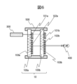
<1.画像表示素子の全体構成>
図6は、実施例の画像表示素子の構成を示している。ここでは画像表示素子10は2枚の導光板100a,100bから構成されており,それぞれ入射回折格子101,出射回折格子102が形成される。
<1. Overall configuration of image display element>
FIG. 6 shows the configuration of the image display element of the example. Here, the
入射回折格子101は,直線状の表面凹凸型の回折格子である。入射回折格子101としては、回折効率が高いブレーズ型回折格子(blazed grating)を例示しているが、種類は特に限定するものではない。
The
出射回折格子102は,それぞれパターン周期が入射回折格子101と同じである。出射回折格子102の表面には,それぞれコーティング層103が形成される。導光板100a、100bはそれぞれ異なるパターン周期P1,P2をもち,対応する波長範囲が異なっている。P1<P2とした場合,導光板100aはカラー画像の波長範囲のうち短波長側の表示に主に機能し,導光板100bは長波長側の表示に主に機能する。P1は例えば360nmであり、P2は例えば460nmである。導光板100の数は任意であり、取り扱う光の波長に応じて一つあるいは3以上の複数でもよい。各導光板のパターン周期は、取り扱う波長に応じて変えることが望ましい。
The pattern period of the
後述の理由により、入射回折格子101は導光板100の映像光の入射面と反対側の面に配置されている。本実施例において,出射回折格子102は入射回折格子101と同じ面に形成される。同一面に両方の回折格子を形成する場合、回折格子パターンを形成するためのスタンパは一枚でよいので、コスト面では有利である。一方、発明者らが出射回折格子の回折効率の検討を行ったところ、導光板100内で導光させるための反射回折を考慮すると、1次反射回折光をユーザに視認させる方が、視認輝度を高くすることができることがわかっている。図6のように入射回折格子101と出射回折格子102をともに映像光の入射面と反対側の面に配置すると、ユーザは1次透過回折光を視認することになり、輝度を向上させる構成が重要になる。なお、入射回折格子101と出射回折格子102をそれぞれ反対側の面に形成することも可能である。
For reasons described later, the
出射回折格子102の形状は、入射回折格子101と同様の直線ストライプ形状でもよいし、図3に示したメッシュ形状でもよい。メッシュ形状にすると、さらに回折効率が高くできる等の効果があるが、他の回折格子の形状を排除するものではない。
The shape of the
本実施例では、出射回折格子102は基本的に導光板100の一つの面にのみ形成されている。すなわち、図6の例では、導光板100の出射回折格子102と反対側の面は、パターンがなく基本的に平坦である。出射回折格子102と反対側の面は、実質的に回折が起こらず光線は理想的には全反射する。導光板100の両面に一つの出射回折格子を分散して配置すると、導光板の熱膨張等で両方の回折格子の位置ずれが生じる可能性がある。
In this embodiment, the
こうした構成によって,プロジェクタ300から出射した映像構成はユーザの瞳400により視認が可能である。プロジェクタ300からの光は、画像表示素子10に対してユーザの瞳400と反対側から入射する。ただし、プロジェクタ300が物理的にユーザの瞳400と反対側に配置される必要はなく、任意の位置に配置したプロジェクタ300からの光線を、ミラー等で導光板100の任意の面から入射させるようにすればよい。
With this configuration, the image configuration emitted from the
図7は1枚の導光板100に形成された入射回折格子101と出射回折格子102の波数ベクトルの関係の一例を示している。前述のように,導光板100が画像表示素子として機能するためには,図において波数K1,K2,K3の大きさが等しく,K1+K2+K3=0となる関係を満たすようにすればよい。
FIG. 7 shows an example of the relationship between the wave number vectors of the
<2.出射回折格子の構成>
図8により、まず,出射回折格子102の具体例について述べる。図8(a)と図8(b)により、同じアスペクト比0.8の場合のフォトニック結晶とメッシュ型回折格子の投影像の比較をした。図8(a)は「特許文献1」に記載のピラー型のフォトニック結晶の斜視図とその投影像のシミュレーション結果である。図8(b)は本実施例のメッシュ型回折格子の斜視図とその投影像のシミュレーション結果である。形状以外の条件は同じである。図に見られるように,アスペクト比1以下の場合,フォトニック結晶では,投影像の中央部の輝度が高く視認性が悪いことがわかる。それに比較して,本実施例のメッシュ型回折格子は低アスペクト比のパターンで良好な投影像を得ることができる。
<2. Configuration of output diffraction grating>
First, a specific example of the
メッシュ型回折格子において、パターンのデューティと回折効率およびアスペクト比の関係をシミュレーションした。回折格子のパターンのピッチをp,パターンの幅をwとすると、デューティはw/pで表される。シミュレーションでは,パターンピッチp=460nm,パターン高さ=70nm,光線の波長=550nm,導光板の厚さ=1.0mm,導光板の屈折率=1.58とした。投影像の視野角は40度である。 We simulated the relationship between pattern duty, diffraction efficiency, and aspect ratio in a mesh-type diffraction grating. When the pitch of the diffraction grating pattern is p and the width of the pattern is w, the duty is expressed as w/p. In the simulation, the pattern pitch p = 460 nm, the pattern height = 70 nm, the wavelength of the light beam = 550 nm, the thickness of the light guide plate = 1.0 mm, and the refractive index of the light guide plate = 1.58. The viewing angle of the projected image is 40 degrees.
シミュレーション結果によると、1次回折効率η1はw/p=0.5で最大値約4.2%となり,w/pが0または1に近づくにつれて低下する特性となっていることが判った。0.6%程度の回折効率を得る場合、本実施例のメッシュ型回折格子のw/pは0.15以上0.85以下の範囲に定める必要がある。また効率が良いのはw/pが0.3以上0.7以下の範囲、効率が最も良いのはw/pが0.4以上0.6以下の範囲であった。 According to the simulation results, it was found that the first-order diffraction efficiency η1 has a maximum value of about 4.2% when w/p=0.5, and has a characteristic that it decreases as w/p approaches 0 or 1. In order to obtain a diffraction efficiency of about 0.6%, the w/p of the mesh type diffraction grating of this example needs to be set in the range of 0.15 or more and 0.85 or less. Furthermore, the best efficiency was found to be in the range of w/p of 0.3 to 0.7, and the best efficiency was found to be in the range of w/p of 0.4 to 0.6.
パターンのアスペクト比に関しては、パターン高さ=70nmで固定としているため、w/pが1または0に近づくと、アスペクト比が増加する。パターンのアスペクト比を1以下にすることを射出成型法等の適応の基準とすると,本実施例のメッシュ型回折格子のw/pは0.15から0.85の範囲に定める必要がある。また、アスペクト比最小で最も製造が容易となるのは、w/p=0.5である。 Regarding the aspect ratio of the pattern, since the pattern height is fixed at 70 nm, as w/p approaches 1 or 0, the aspect ratio increases. Assuming that the aspect ratio of the pattern is 1 or less as a criterion for application of injection molding, etc., the w/p of the mesh type diffraction grating of this embodiment needs to be set in the range of 0.15 to 0.85. Furthermore, the aspect ratio that is the smallest and the easiest to manufacture is w/p=0.5.
以上から、原理的にはw/p=0.5、すなわちw=p-wのとき、メッシュ型回折格子の回折効率が最大かつ、パターンのアスペクト比最小ということがいえる。 From the above, it can be said that in principle, when w/p=0.5, that is, w=pw, the diffraction efficiency of the mesh type diffraction grating is maximum and the aspect ratio of the pattern is minimum.
図9により次に,入射回折格子101の具体例について述べる。
Next, a specific example of the
<3.入射回折格子の構成>
図9(a)は「特許文献3」と同じ透過型の回折格子のシミュレーション結果である。透過型回折格子は,入射した光が透過回折して,導光板(基板)100内部を伝搬する。入射回折格子101の位置は,導光板100の光源に近い面に形成される。
<3. Configuration of input diffraction grating>
FIG. 9(a) is a simulation result of the same transmission type diffraction grating as in "
映像光線1000は左から入射する構成であり,図の右半分が基板(Sub)を表している。透過型の回折格子では,ブレーズ面による屈折と周期構造による回折が位相同調する条件で最大の回折効率が得られる。図に示すように,これを実現するには凹凸パターンの高さが大きい必要があり,パターンの角度は70度から80度,パターンの高さを周期で割ったアスペクト比は10以上が必要である。射出成型等の一般のプラスチック成型法では,アスペクト比が1を超えると転写性の悪化等の問題が生じて,量産時の歩留りが低下する。ここに示した透過型の回折格子は本実施例の入射回折格子としては適していないことが判る。
The
図9(b)は反射型の回折格子のシミュレーション結果である。反射型の回折格子では、入射した光が反射回折して,すなわち,光源側に反射して導光板(基板)100の内部を伝播する。入射回折格子101の位置は,導光板100の光源から遠い面に形成される。
FIG. 9(b) shows simulation results for a reflective diffraction grating. In the reflection type diffraction grating, the incident light is reflected and diffracted, that is, reflected toward the light source side and propagated inside the light guide plate (substrate) 100. The position of the
映像光線1000は同様に左から入射する構成であり,図の左半分が基板(Sub)を表している。反射型の回折格子では,ブレーズ面による反射と周期構造による回折が位相同調する条件で最大の回折効率が得られる。図に見られるように,透過型に比較して,低いアスペクト比の凹凸パターンでこの条件が満たされることが判る。このときの凹凸パターンの高さは約250nmであり,アスペクト比は約0.57である。前述の試作素子では,パターン高さが374nmの三角形状の凹凸パターンを良好に転写可能であった。プラスチック形成を採用した本実施例の導光板に好適な入射回折格子は、反射型の入射回折格子であると言える。
The
<4.導光板の傾きの影響の検討>
図10Aおよび図10Bは、2枚の導光板100の相対傾きの影響を示す摸式図である。図10Aおよび図10Bにおいて,導光板100はそれぞれ対応波長が異なる導光板100aと100bで構成される。また,300は映像投影用のプロジェクタ,400はユーザの瞳,500は投影される映像光線を表している。
<4. Examination of the influence of the tilt of the light guide plate>
FIGS. 10A and 10B are schematic diagrams showing the influence of the relative inclination of the two
この例では、図9で説明した知見に基づいて、入射回折格子は反射型の回折格子を採用した。そのため、入射回折格子101は,導光板100のプロジェクタ300から遠い面(図中では右面)に形成される。出射回折格子102は,プロセスの都合上,入射回折格子101とおなじ面に形成する方が精度を高くできるので,同じくプロジェクタ300から遠い面に形成される。
In this example, a reflective diffraction grating was used as the incident diffraction grating based on the knowledge explained with reference to FIG. Therefore, the
図10Aはプロジェクタ300とユーザの瞳400が導光板100に対して同じ側に配置される場合である。図に示すように,導光板100は最終的に映像光線500を反射してユーザの瞳400に届ける。このため,導光板100aに比較して導光板100bが傾いていると、投影される光線の波長によって,視認される画素位置がシフトして,画質が低下する。視力1.0のユーザの光線角度の分解能力は1/60度であるから,これを基準とすると2枚の導光板の相対傾きは1/60度よりも十分に小さくする必要があり,従来のガラス製に比較して機械強度(ヤング率)の小さなプラスチック導光板ではヘッドマウントディスプレイとしての実装が難しい。この場合,出射回折格子の反射回折効率が高いほど,輝度の高い映像情報をユーザに提供することができる。
FIG. 10A shows a case where the
図10Bはプロジェクタ300とユーザの瞳400が導光板100に対して反対側に配置される場合である。図に示すように,導光板100は最終的に映像光線500を透過してユーザの瞳400に届ける。入射光と出射光の角度は基本的に同じため,導光板100aと100bの相対傾きがあっても原理的に波長による投影像のシフトは発生しない。したがって,本実施例のプラスチック製導光板をヘッドマウントディスプレイに実装する場合には,プロジェクタ光源を導光板100に対してユーザの瞳400と反対側(透過型の光学構成)にすることが望ましい。
FIG. 10B shows a case where the
実際には,導光板内部を全反射導光する光線角度条件が影響を受けるため,導光板100aと100bの相対傾きは3度程度以下に抑えることが望ましいことを付記しておく。この場合,出射回折格子102の透過回折効率が高いほど,輝度の高い映像情報をユーザに提供することができる。
It should be noted that in reality, it is desirable to suppress the relative inclination of the
<5.視認輝度向上の検討と出射回折格子の改善>
導光板100を伝搬中の光が出射回折格子102で回折して,導光板100から出射する際の回折効率をFDTD法で計算した。波長550nm,導光板の屈折率1.58,回折格子のパターン周期460nm,凸部の幅150nm,凸部の高さ70nmとして,投影像の中央画素に相当する光が入射回折でカップリングして導光板内部を全反射伝搬している条件において,反射回折効率が3.5%,透過回折効率が2.8%となった。凹凸パターンのアスペクト比は0.47である。図10Bと同様に出射回折格子102が,入射回折格子101と同じ面に形成されている場合,ユーザに視認される光線は出射回折格子102で透過回折したものである。したがって,図10Bに示した透過型の光学構成では,図10Aの反射型の光学構成に比較して,ユーザに視認される投影像の輝度が低下してしまう。
<5. Consideration of improving visible brightness and improvement of output diffraction grating>
The diffraction efficiency when light propagating through the
図11は、出射回折格子102上の薄膜コーティングをスパッタリング法で形成し、ZnS-SiO2(20%)薄膜(屈折率2.33)として,当該誘電体薄膜の膜厚を横軸に示し、透過回折効率および,導光板の透過率を縦軸に示したものである。
In FIG. 11, a thin film coating on the
ここでは,導光板100を伝搬中の光が出射回折格子102で回折して,導光板100から出射する際の透過回折効率をFDTD法で計算した。波長550nm,導光板100の屈折率1.58,出射回折格子102のパターン周期460nm,凸部の幅150nm,凸部の高さ70nmとして,投影像の中央画素に相当する光が入射回折格子101でカップリングして導光板100内部を全反射伝搬している条件においての透過回折効率の計算をした。
Here, the transmission diffraction efficiency when light propagating through the
図11(a)に見られるように,出射回折格子102の上に誘電体薄膜を形成することによって,透過回折効率が向上し,輝度の高い映像情報を提供することが可能となる。視認輝度を重要視した場合、誘電体膜の膜厚を70nmとすると,透過回折効率が7.3%となり,コーティングを施さない場合の2.8%に比較して2.5倍以上の効率向上を図ることが可能である。誘電体膜の膜厚を170nmとすると,透過回折効率が9.3%となり,コーティングを施さない場合の2.8%に比較して3倍以上の効率向上を図ることが可能である。
As shown in FIG. 11(a), by forming a dielectric thin film on the
また,回折効率の向上は,反射回折効率にも表れ,約20nm以上の膜厚を形成した場合,コーティングを施さない場合の反射回折効率を上回ることができる。このため,出射回折格子102を入射回折格子101と同じ面に形成しても、大きな輝度を得ることができる。
Furthermore, the improvement in diffraction efficiency is also reflected in the reflection diffraction efficiency, and when a film thickness of approximately 20 nm or more is formed, the reflection diffraction efficiency can be exceeded when no coating is applied. Therefore, even if the
図11(b)は導光板の透過率の計算結果であり,ユーザが外界を視認する場合の明るさに対応している。例えば,ZnS-SiO2(20%)薄膜の場合,その厚さ70nmとした場合,導光板の透過率は,誘電体薄膜を形成しない場合の約91%に比較して約72%に低下する。これは,例えばユーザが屋外で本実施例のヘッドマウントディスプレイを使用するときに,強い外光の像を約8割(=72%/91%)に減光すると共に,投影像の輝度を約2.5倍(7.3%/2.8%)に向上させることによって投影像の視認性を高める効果がある。また、誘電体膜の膜厚を170nmとすると,さらに投影像の明るさが外界に比較して明るく見える。図11(b)によると、膜厚が70nm以上、170nm以下の範囲では、透過率は68~80%になり、回折効率向上の効果を考慮すると、外界に対する投影像の相対的な輝度を向上することが可能である。 FIG. 11(b) shows the calculation result of the transmittance of the light guide plate, which corresponds to the brightness when the user visually recognizes the outside world. For example, in the case of a ZnS-SiO 2 (20%) thin film, when the thickness is 70 nm, the transmittance of the light guide plate decreases to about 72% compared to about 91% when no dielectric thin film is formed. . For example, when a user uses the head mounted display of this embodiment outdoors, this reduces the brightness of the projected image by about 80% (=72%/91%) and reduces the brightness of the projected image. By increasing the visibility by 2.5 times (7.3%/2.8%), there is an effect of increasing the visibility of the projected image. Furthermore, when the thickness of the dielectric film is 170 nm, the brightness of the projected image appears even brighter compared to the outside world. According to Figure 11(b), when the film thickness is in the range of 70 nm or more and 170 nm or less, the transmittance is 68-80%, and considering the effect of improving diffraction efficiency, the relative brightness of the projected image with respect to the outside world is improved. It is possible to do so.
一般に,スパッタリング法等により形成された誘電体薄膜は,装置,ターゲット,真空度,RF(高周波)電力等の成膜条件により,密度や内部応力が変化する。本実施例では,発明者らが成膜した誘電体薄膜について,分光光度計による反射率と透過率の測定結果を用いて屈折率を同定したものである。他の成膜方法や装置で誘電体薄膜を形成する場合には,屈折率が±5%程度は異なる場合があるので付記しておく。 Generally, the density and internal stress of dielectric thin films formed by sputtering and the like vary depending on film forming conditions such as equipment, target, degree of vacuum, and RF (radio frequency) power. In this example, the refractive index of the dielectric thin film formed by the inventors was identified using the results of measuring reflectance and transmittance using a spectrophotometer. It should be noted that if the dielectric thin film is formed using other film forming methods or devices, the refractive index may differ by about ±5%.
本実施例に好適な薄膜材料としては,ここに示したZnS-SiO2(20%)のほかにZnS,AlN,SiNx,SiO,AlON,Al2O3,等の誘電体材料を用いることができる。 In addition to the ZnS-SiO 2 (20%) shown here, dielectric materials such as ZnS, AlN, SiNx, SiO, AlON, Al 2 O 3 can be used as thin film materials suitable for this example. can.
本実施例によれば、表面凹凸型の回折格子を有する導光板(画像表示素子)において,出射回折格子の表面にスパッタリング法等により誘電体材料等のコーティング層を形成することで,出射光の回折効率を4%以上に増加させることが可能となる。メッシュ型の出射回折格子を用いれば,射出成型法等により導光板のプラスチック化を実現し,安全で軽量で輝度の高い導光板を実現することができる。 According to this embodiment, in a light guide plate (image display element) having a diffraction grating with an uneven surface, a coating layer of a dielectric material or the like is formed on the surface of the output diffraction grating by sputtering or the like, so that the output light can be It becomes possible to increase the diffraction efficiency to 4% or more. If a mesh-type output diffraction grating is used, the light guide plate can be made of plastic using injection molding, etc., and a light guide plate that is safe, lightweight, and has high brightness can be realized.
本実施例においては,ユーザの視認する画像の輝度分布の平滑化に着目して導光板の表示性能を改善する実施例について示す。 In this example, an example will be described in which the display performance of the light guide plate is improved by focusing on smoothing the brightness distribution of the image visually recognized by the user.
<2-1.輝度分布の平滑化の検討>
導光板100を伝搬中の光が出射回折格子102で回折して,導光板100から出射する際の透過回折効率をFDTD法で計算し,透過回折効率の入射角依存をテーブル化した。これを用いて光線追跡を行い,ユーザが視認する像を求めた。ここでは,波長635nm,導光板の屈折率1.58,回折格子のパターン周期460nm,凸部の幅150nm,凸部の高さ90nmとした。また,導光板100の厚さを1mmとし,入射回折格子101に入射する映像光線の直径は4mm,入射回折格子101と出射回折格子102の間の距離を5mm,導光板100からユーザの瞳400までの距離を25mm,ユーザの瞳400の直径を3mmとした。
<2-1. Consideration of smoothing luminance distribution>
The transmission diffraction efficiency when the light propagating through the
図12は,計算に用いた物体モデルの一例である。プラスチック製の導光板100の表面には凹凸パターンの出射回折格子102が形成され,その上に,一定の膜厚で誘電体薄膜のコーティング層103を形成したとしている。実際には,凹凸パターンには傾斜角がともない台形に近い断面形状となるが,ここでは計算モデルの簡素化のため,理想的な矩形回折格子を断面形状として仮定している。誘電体材料としては,ZnS-SiO2(20%)の結果である。図中黒色で示した部分1200は空気層を示している。
FIG. 12 is an example of an object model used for calculation. An
図13は,計算した視認像の一例である。表示ピクセルを1280x720ピクセルとして,ここでは,横方向をX方向,縦方向をY方向としている。入射回折格子の波数ベクトルはY方向である。表示像のY方向のピクセル位置により,映像光線の入射角および導光板内の伝搬角が変化する。 FIG. 13 is an example of the calculated visible image. The display pixels are 1280x720 pixels, and here, the horizontal direction is the X direction and the vertical direction is the Y direction. The wave number vector of the incident grating is in the Y direction. The incident angle of the image light beam and the propagation angle within the light guide plate change depending on the pixel position in the Y direction of the displayed image.
図14A~図14Cは,Y方向のピクセル位置に対する計算結果を示している。コーティング層103の材料は,ZnS-SiO2(20%)とした。
14A to 14C show calculation results for pixel positions in the Y direction. The material of the
図14Aは,導光板100内部を伝搬する光線の角度,すなわち出射回折格子102への入射角を示している。ピクセル位置が大きくなると入射角が小さくなることが判る。
FIG. 14A shows the angle of the light beam propagating inside the
図14Bは,透過回折効率の計算結果である。ここでは,コーティング層103の膜厚を0,25,35nmの3種類の場合について示している。図にみられるように,コーティング層103を形成しない場合(厚さ0nm)では,ピクセル位置の増加に従って,透過回折効率が増加していることが判る。一方で,誘電体薄膜を形成した場合,例えば,35nm形成すると,ピクセル位置の増加に従って,透過回折効率を減少させることができることが判る。また、25nm形成すると,ピクセル位置の増加に対して透過回折効率が比較的変化しないことが判る。
FIG. 14B shows the calculation results of transmission diffraction efficiency. Here, three types of thicknesses of the
図14Cは,ユーザが視認する輝度の計算結果である。図にみられるように,誘電体薄膜を形成しない場合(厚さ0nm)では,ピクセル位置の増加に従って,輝度の増加が顕著である。また、誘電体膜厚35nmの場合,中央部での輝度は高いが、ピクセル位置の増加に従って,輝度の減少が顕著である。一方で,誘電体膜厚25nmの場合,ピクセル位置によらず,平坦な輝度分布の像を提供することが可能になる。よって、誘電体膜厚25nm以上、35nm未満で輝度向上と平坦な輝度分布の両立が図れることになる。 FIG. 14C shows the calculation result of the luminance visually recognized by the user. As seen in the figure, when no dielectric thin film is formed (thickness: 0 nm), the brightness increases significantly as the pixel position increases. Furthermore, in the case of a dielectric film thickness of 35 nm, the brightness at the center is high, but as the pixel position increases, the brightness decreases significantly. On the other hand, when the dielectric film thickness is 25 nm, it becomes possible to provide an image with a flat luminance distribution regardless of the pixel position. Therefore, with a dielectric film thickness of 25 nm or more and less than 35 nm, it is possible to achieve both improved brightness and a flat brightness distribution.
本実施例によれば,出射回折格子の表面に誘電体薄膜を形成することにより,ユーザが視認する像の輝度分布を制御することができる。上記の例では、誘電体膜厚25nmの場合、輝度分布を平坦に近づけることが可能である。 According to this embodiment, by forming a dielectric thin film on the surface of the output diffraction grating, it is possible to control the brightness distribution of the image visually recognized by the user. In the above example, when the dielectric film thickness is 25 nm, it is possible to make the luminance distribution close to flat.
<2-2.膜材料と屈折率の検討>
本実施例に好適な薄膜材料としては,ZnS,AlN,SiNx,SiO,AlON,Al2O3,等の誘電体材料を用いることができるほか,ZnS-SiO2(20%)のように2種以上の誘電体の混合材料を用いることもできる。
<2-2. Consideration of film material and refractive index>
As the thin film material suitable for this example, dielectric materials such as ZnS, AlN, SiNx, SiO, AlON, Al 2 O 3 can be used, as well as dielectric materials such as ZnS-SiO 2 (20%). Mixed materials of more than one dielectric material may also be used.
図15Aは,本実施例に好適な誘電体材料の屈折率の範囲を示すシミュレーション結果である。上に示した各種の誘電体材料で形成するコーティング層103の膜厚は,ZnS-SiO2(20%)の膜厚35nm(=0.128λ,λ=635nm)と比較するため,屈折率で規格化し,同じ0.128λとした。
FIG. 15A is a simulation result showing the range of refractive index of the dielectric material suitable for this example. The film thickness of the
図において縦軸は投影像の中央の輝度向上に関与する透過回折効率を、コーティング層103がない場合を1として規格化したものである。図に見られるように,出射回折格子102の上に形成するコーティング層103の屈折率が大きくなるに従って,透過回折効率が増加し,視認される像の輝度が向上する効果があることが判る。
In the figure, the vertical axis represents the transmission diffraction efficiency, which is involved in improving the brightness at the center of the projected image, which is normalized to 1 when there is no
図15Bは,図15Aの一部を拡大したものである。本実施例の誘電体膜の効果により回折効率が1.2倍あれば,同じ明るさの像をユーザに視認させる場合、誘電体膜がない場合に比較して光源の消費電力が20%低減可能となる。この条件を本実施例による効果が顕在化する条件とすると,誘電体材料の屈折率が1.64以上であればよいことが判る。 FIG. 15B is a partially enlarged view of FIG. 15A. If the diffraction efficiency is 1.2 times higher due to the effect of the dielectric film in this example, the power consumption of the light source will be reduced by 20% compared to the case without the dielectric film when making an image of the same brightness visible to the user. It becomes possible. If this condition is used as a condition for the effect of this example to become apparent, it is understood that the refractive index of the dielectric material should be 1.64 or more.
本実施例に好適な薄膜材料としては,ZnS,AlN,SiNx,SiO,AlON,Al2O3,等の誘電体材料を用いることができるほか,ZnS-SiO2(20%)のように2種以上の誘電体の混合材料を用いることもできる。公知な誘電体材料としてはダイアモンドが最も高い屈折率(2.42)であり,図15Aに示したように,本実施例に好適な誘電体薄膜の屈折率の上限は2.42である。 As the thin film material suitable for this example, dielectric materials such as ZnS, AlN, SiNx, SiO, AlON, Al 2 O 3 can be used, as well as dielectric materials such as ZnS-SiO 2 (20%). Mixed materials of more than one dielectric material may also be used. Diamond has the highest refractive index (2.42) among known dielectric materials, and as shown in FIG. 15A, the upper limit of the refractive index of the dielectric thin film suitable for this example is 2.42.
図16Aは,本実施例に好適な誘電体材料の膜厚範囲を示すシミュレーション結果である。誘電体材料としては,ZnS(屈折率2.355)とした。図において縦軸は投影像の中央の輝度向上に関与する透過回折効率を規格化したものである。図に見られるように,出射回折格子の上に形成する誘電体膜の膜厚が厚くなるに従って,透過回折効率が増加し,視認される像の輝度が向上する効果があることが判る。膜厚が約70nm以上であれば、膜がない場合の約3倍以上の回折効率が得られている。 FIG. 16A is a simulation result showing the film thickness range of the dielectric material suitable for this example. ZnS (refractive index 2.355) was used as the dielectric material. In the figure, the vertical axis is the normalized transmission diffraction efficiency that is involved in improving the brightness at the center of the projected image. As seen in the figure, it can be seen that as the thickness of the dielectric film formed on the output diffraction grating increases, the transmission diffraction efficiency increases, which has the effect of improving the brightness of the visually recognized image. When the film thickness is about 70 nm or more, the diffraction efficiency is about three times or more than when there is no film.
図16Bは,平坦な基板上の形成した誘電体薄膜,いわゆる光学薄膜コーティングの反射率の膜厚依存性である。ここでは上と同様に基板の屈折率を1.58とし,誘電体材料としてZnSを選び,その膜厚と反射率の関係を計算した。図に見られるように,膜厚に対して,周期的に反射率が変化することが判る。こうした誘電体薄膜の膜厚依存性は周知である。一方,図16Aに示したように,回折格子上の誘電体薄膜では,周期性のほかに膜厚の増加に対する回折効率の単調増加成分が含まれる特性となることが特徴である。こうした知見は,ヘッドマウントディスプレイを扱う公知技術に開示されていない点であり,発明者らが見出した特性である。 FIG. 16B shows the film thickness dependence of the reflectance of a dielectric thin film formed on a flat substrate, a so-called optical thin film coating. Here, as above, the refractive index of the substrate was set to 1.58, ZnS was selected as the dielectric material, and the relationship between its film thickness and reflectance was calculated. As seen in the figure, it can be seen that the reflectance changes periodically with the film thickness. Such thickness dependence of dielectric thin films is well known. On the other hand, as shown in FIG. 16A, the dielectric thin film on the diffraction grating is characterized by a characteristic that includes, in addition to periodicity, a monotonically increasing component of diffraction efficiency as the film thickness increases. This knowledge is not disclosed in the known technology dealing with head-mounted displays, and is a characteristic discovered by the inventors.
図16Cは,図16Aを拡大したものである。本実施例の効果により回折効率が1.2倍以上となる条件を本実施例による効果が顕在化する条件とすると,誘電体材料の膜厚は10nm以上であればよいことが判る。ただし,本実施例においては,図12に示したように,回折格子上に形成した誘電体薄膜が,元の回折格子の凹凸形状に沿って形成されることが必要であり,膜厚が凹凸パターンの高さ(略100nm)の10倍(略1000nm)を超えると,誘電体薄膜表面の凹凸形状が次第に失われ平坦に近づくことが,スパッタリング法や真空蒸着法などの成膜プロセスに依存して定まっていることも公知である。したがって,本実施例の効果が現れる膜厚の上限は略1000nmである。 FIG. 16C is an enlarged version of FIG. 16A. If the conditions under which the effect of this example makes the diffraction efficiency 1.2 times or more are the conditions under which the effect of this example becomes apparent, it can be seen that the film thickness of the dielectric material only needs to be 10 nm or more. However, in this example, as shown in FIG. 12, the dielectric thin film formed on the diffraction grating needs to be formed along the uneven shape of the original diffraction grating, and the film thickness is uneven. If the height exceeds 10 times (approximately 1000 nm) the height of the pattern (approximately 100 nm), the uneven shape of the dielectric thin film surface gradually disappears and becomes flat, depending on the film formation process such as sputtering or vacuum evaporation. It is also known that it is fixed. Therefore, the upper limit of the film thickness at which the effect of this embodiment appears is approximately 1000 nm.
実施例3では入射回折格子101に好適な誘電体薄膜について検討する。以下で説明する入射回折格子101は反射型回折格子であり、該反射型回折格子の上に多層コーティング層を備える。多層コーティング層は、第1の誘電体薄膜と第2の誘電体薄膜を交互に形成した周期構造を有することで、優れた波長依存性を得ることができる。
In Example 3, a dielectric thin film suitable for the
図17は導光板ごとの表示像の範囲のシミュレーション結果である。ここでは,図6に示したように2枚の導光板100a(短波長用),100b(長波長用)で構成された導光板の場合について示す。入出射回折格子のピッチは導光板100a(短波長用)が360nm,導光板100b(長波長用)が460nm,表示像の対角視野角は35度,アスペクト比は16:9である。図17に画面イメージを示すように,各導光板の画像の表示範囲(図中の白い部分で示される)が異なることが判る。
FIG. 17 shows the simulation results of the display image range for each light guide plate. Here, as shown in FIG. 6, a case will be described in which the light guide plate is composed of two
こうした構成では,表示像の色を一般的にR(赤)G(緑)B(青)とすると,導光板100aはB像(青色表示像)とG像(緑色表示像)の一部の表示に寄与し,導光板100bはG像(緑色表示像)の一部とR像(赤色表示像)の表示に寄与している。図6における導光板100aに設けられた入射回折格子101aは,B波長(青色波長)を大きな回折効率で反射回折し,G波長(緑色波長)をそれよりも小さな回折効率で反射回折し,R波長(赤色波長)をほぼ透過することが望ましいことが判る。これは回折効率に強い波長依存性が求められることを意味する。
In such a configuration, if the colors of the displayed images are generally R (red), G (green), and B (blue), the
一般に,このような短波長の光線を反射し,長波長の光線を透過する光学素子として,ダイクロイック・フィルムが知られており,透明基板上に形成された誘電体多層薄膜で実現できる。ところが,図16Aに示したように,表面凹凸回折格子の上に形成する誘電体薄膜は,一般の光学薄膜と異なる膜厚依存性を示す。ここでは,入射回折格子の上に形成するのに好適な誘電体薄膜の条件について示す。導光板100a(短波長用)の主たる性能示数は反射1次回折効率と透過率である。
Generally, a dichroic film is known as an optical element that reflects such short-wavelength light and transmits long-wavelength light, and can be realized by a dielectric multilayer thin film formed on a transparent substrate. However, as shown in FIG. 16A, the dielectric thin film formed on the surface uneven diffraction grating exhibits thickness dependence that is different from that of general optical thin films. Here, conditions for a dielectric thin film suitable for forming on the incident diffraction grating will be described. The main performance indicators of the
図18は、本実施例の画像表示素子の別の構成を示している。ここでは画像表示素子10は2枚の導光板100a,100bから構成されており,それぞれ入射回折格子101a,101b,出射回折格子102a,102bが形成される。入射回折格子101a,101bは,直線状あるいは格子状の表面凹凸型の回折格子である。出射回折格子102a,102bは,それぞれパターン周期が入射回折格子101a,101bと同じである。
FIG. 18 shows another configuration of the image display element of this example. Here, the
出射回折格子102a,102bの表面には,それぞれコーティング層103a,103bが形成される。導光板100a,100bはそれぞれ異なるパターン周期P1,P2をもち,対応する波長範囲が異なっており,P1<P2とした場合,導光板100aはカラー画像の波長範囲のうち短波長側の表示に主に機能し,導光板100bは長波長側の表示に主に機能する。図18において,図6との構成上の差異は,入射回折格子101a,101bの上にも,誘電体膜でコーティング層104a,104bを形成している点にある。
図19は、反射型の入射回折格子101の断面形状を示す摸式図である。図9に示したように本実施例の導光板には反射型の入射回折格子が適している。ここでは,断面形状を高さ5レベルとした階段状の凹凸型回折格子を例示している。図中,凹凸形状の最も高さが低い点をz=0とし,x方向は回折格子の周期方向としている。回折格子のピッチはP,光線の波長はλである。
FIG. 19 is a schematic diagram showing the cross-sectional shape of the reflection type
紙面下側から入射した入射光1901は,紙面右下方向に反射1次回折され回折光1902となる。図中に示すように,ピッチPだけ離れて入射した入射光1901は回折方向にそれぞれ1λの光路差をもつ。これらの回折光は全て位相差が1λ(=2π)であるので,強め合いにより特定の方向(周期Pが波長λに対応する方向)に回折する。これは,広く知られた回折の基本原理である。本実施例の入射回折格子101に好適な誘電体コーティングを考察するため,この基本原理を回折格子の高さz方向に拡張する。
図20は、本実施例に好適な誘電体コーティングを考察するための摸式図である。上述のように,回折光1902に対して,入射回折格子101のピッチPは選択するべき波長λに対応して定めた。図中の破線は高さ変調された回折格子の形状を周期的に拡張したものである。x方向に1周期Pだけシフトした点の高さはHだけ異なる。ここでは,Hを入射回折格子101の周期高さと定義する。破線状の形状の仮想回折格子からも同様に同じ角度の回折光が発生し,回折光に対して,回折格子の周期高さHは波長λに対応する。
FIG. 20 is a schematic diagram for considering a dielectric coating suitable for this example. As described above, the pitch P of the
実際の回折格子の最大高さをhとすると,この例ではH=5h/4である。本実施例の入射回折格子101に好適な誘電体コーティングは,少なくとも屈折率の高い材料(屈折率n1,膜厚d1)と屈折率の低い材料(屈折率n2,膜厚d2)の2種を用い,これを回折格子の上に交互に積層する。このとき,回折格子の表面よりも,z方向上側に,回折格子の表面凹凸形状を反映した誘電体層が形成される。本実施例に好適な条件は,d1+d2≒Hである。このとき,誘電体層は図20中の破線に沿って境界が形成され,これらから発生する回折光1902は,位相差が2πで強めあうことができる。これが,本実施例の入射回折格子上に形成する誘電体コーティングの基本概念である。
If the actual maximum height of the diffraction grating is h, then in this example H=5h/4. The dielectric coating suitable for the
図21は、回折格子の周期高さHと1周期の高さ形状の関係をまとめたものである。ここに示すように,高さ5,4,3,2レベルの階段状回折格子,およびブレーズ型回折格子,一般形状の回折格子において,周期高さHは図に示す値として定義される。図に示すような等幅の階段状回折格子の場合,高さがNレベル,最大高さがhとすると,
H=(N/N-1)h
となる。
FIG. 21 summarizes the relationship between the periodic height H of the diffraction grating and the height shape of one period. As shown here, in stepped diffraction gratings with heights of 5, 4, 3, and 2 levels, blazed diffraction gratings, and diffraction gratings with general shapes, the periodic height H is defined as the value shown in the figure. In the case of a stepped diffraction grating with equal width as shown in the figure, if the height is N level and the maximum height is h, then
H=(N/N-1)h
becomes.
ブレーズ型回折格子では,図示するように,主たるブレーズ面の傾きから高さを1周期に拡張したものが周期高さHである。いわゆるブレーズ角はθBである。このとき,
H={(p1+p2)/p1}h
となる。
In a blazed diffraction grating, as shown in the figure, the periodic height H is the height expanded to one period from the inclination of the main blazed surface. The so-called blaze angle is θ B. At this time,
H={(p 1 +p 2 )/p 1 }h
becomes.
一般形状の回折格子でも同様に,平均傾きからブレーズ角θBを定めることにより,回折格子周期をPとすると
H=P・tanθB
となる。
Similarly, for a general-shaped diffraction grating, by determining the blaze angle θ B from the average inclination, if the diffraction grating period is P, then H=P・tanθ B
becomes.
図22Aは、本実施例の入射回折格子101の断面形状を示すシミュレーションモデルである。射出成型法等により,プラスチック基板上に表面凹凸として高さ3レベルの回折格子を形成した場合を示している。図中の補助線は,上に示した高さ方向の等位相線610を表しており,回折格子の周期性から,図中X方向に一周期右にシフトすることにより,等位相線610と凹凸パターンのZ方向の距離はH,2H,3H,のように周期高さHずつ等間隔に大きくなる。本モデルにおいて,回折格子の高さhは100nm,周期は360nmである。入射回折格子101を構成するプラスチック基板の屈折率は、基板をポリカーボネートとして,1.58,周期高さHは150nmである。図中黒い部分は空気層(Air)である。
FIG. 22A is a simulation model showing the cross-sectional shape of the
図22Bは、本実施例の入射回折格子101の断面形状を示すシミュレーションモデルである。ここでは,入射回折格子101の上に高屈折率の第1の誘電体膜221(屈折率n1,厚さd1)と低屈折率の第2の誘電体膜222(屈折率n2,厚さd2)を交互に221-1、222-1、221-2、222-2、221-3のように順次形成して,5層の誘電体薄膜を積層した場合を示している。ここでは,n1>n2,d1+d2=Hである。こうした条件により,誘電体層によりz方向に形成された回折格子群は,等位相面610a,610b,610c等の上に整列して形成することができる。前述のように,これらの回折格子群から発生する回折光は位相整合し,大きな回折効率を得ることができる。シミュレーションでは,第1の誘電体膜221としてZnS-SiO2(20%)を選択しn1=2.33,d1=55nm,第2の誘電体膜222としてSiO2を選択しn2=1.47,d2=95nmとした。回折格子のピッチは選択する波長(ここでは青色光)に対応して定める。
FIG. 22B is a simulation model showing the cross-sectional shape of the
図23Aは、リファレンスとして,高さ3レベルの入射回折格子101の上にAl膜231を100nm積層した場合のシミュレーションモデルである。
FIG. 23A is a simulation model in which a 100 nm
図23Bは、リファレンスとして,ブレーズ型の入射回折格子101の上にAl膜231を100nm積層した場合のシミュレーションモデルである。
FIG. 23B is a simulation model in which a 100 nm
図24Aは、図22Bに示した本実施例の高さ3レベルの回折格子上に5層の誘電体薄膜を形成した入射回折格子の反射1次回折効率と透過率のシミュレーション結果である。ここでは,表示像の中央に相当する入射角0度の場合を計算している。図に見られるように,反射1次回折効率はB(青,460nm)波長帯からG(緑,530nm)波長帯で大きく,R(赤,640nm)波長帯でゼロであり,最大はB波長帯で約80%となる。また,透過率はB波長帯で20%程度,R波長帯で80%以上と,図18で説明した短波長用の導光板100aに好適な波長依存性を提供できることが判る。
FIG. 24A is a simulation result of the reflection first-order diffraction efficiency and transmittance of the incident diffraction grating in which five dielectric thin films are formed on the three-level diffraction grating of the present example shown in FIG. 22B. Here, the case where the incident angle is 0 degrees corresponding to the center of the displayed image is calculated. As seen in the figure, the reflection first-order diffraction efficiency is large from the B (blue, 460 nm) wavelength band to the G (green, 530 nm) wavelength band, and is zero in the R (red, 640 nm) wavelength band, and the maximum is at the B wavelength. It is about 80% in the belt. Further, the transmittance is about 20% in the B wavelength band and 80% or more in the R wavelength band, which indicates that suitable wavelength dependence can be provided for the
図24Bは、図23Aに示した高さ3レベルの回折格子上にAl薄膜を形成した入射回折格子のシミュレーション結果である。B波長帯の回折効率は約50%,透過率は全波長域でほぼゼロである。 FIG. 24B is a simulation result of an incident diffraction grating in which an Al thin film is formed on the diffraction grating with three height levels shown in FIG. 23A. The diffraction efficiency in the B wavelength band is about 50%, and the transmittance is almost zero in the entire wavelength range.
図24Cは、図23Bに示したブレーズ型回折格子上にAl薄膜を形成した入射回折格子のシミュレーション結果である。B波長帯の回折効率は約50%,透過率は全波長域でほぼゼロである。 FIG. 24C is a simulation result of an incident diffraction grating in which an Al thin film is formed on the blazed diffraction grating shown in FIG. 23B. The diffraction efficiency in the B wavelength band is about 50%, and the transmittance is almost zero in the entire wavelength range.
以上のように,本実施例により,誘電体膜を積層した入射回折格子では,Al反射膜を形成したブレーズ型回折格子よりも大きな回折効率と,長波長帯での大きな透過率を両立可能であることが判った。これは,導光板の入射回折格子として好適な性能特性である。 As described above, according to this example, the incident diffraction grating with laminated dielectric films can achieve both higher diffraction efficiency and higher transmittance in the long wavelength band than the blazed diffraction grating with an Al reflective film. I found out something. This is a suitable performance characteristic as an incident diffraction grating for a light guide plate.
図25は、図22Bの誘電体薄膜に対して,合計厚さ(d1+d2)が周期高さHからずれた場合のシミュレーション結果である。ここでは,第2の誘電体膜222の膜厚d2を変化させて,B波長帯の反射1次回折効率を計算した結果を示している。軸は(d1+d2)/Hであり,この値が1の場合が位相整合の条件である。前述のように,入射回折格子にAl反射膜を形成した場合の回折効率は約50%であった。これよりも大きな回折効率が得られる条件を本実施例の効果が顕在化する条件として定義すると,(d1+d2)/Hの範囲がおおよそ0.7~1.3の範囲になることが判る。すなわち、0.7H<d1+d2<1.3Hである。
FIG. 25 shows simulation results when the total thickness (d1+d2) deviates from the periodic height H for the dielectric thin film shown in FIG. 22B. Here, the results of calculating the reflection first-order diffraction efficiency in the B wavelength band are shown while changing the film thickness d2 of the
前述のように,本実施例の多層誘電体コーティングにおいて回折格子の周期高さHが光線の位相2π(360度)に相当する。したがって,ここに示した条件範囲は位相差が±110に相当し,波動の重ね合わせ条件に照らしてもリーズナブルな結果になっていると言える。 As described above, in the multilayer dielectric coating of this embodiment, the periodic height H of the diffraction grating corresponds to the phase 2π (360 degrees) of the light beam. Therefore, the condition range shown here corresponds to a phase difference of ±110, which can be said to be a reasonable result even in light of the wave superposition conditions.
以上では、短波長用の導光板100aについて説明したが、長波長用の導光板100bに対しても、回折格子のピッチを選択する波長(例えば赤色光)に対応して定めることで、同様の効果を得ることができる。
Although the
図26は本実施例の誘電体薄膜を13層積層した場合の膜形状を示す摸式図である。前述のように,真空蒸着法やスパッタリング法などにより,プラスチック形成の入射回折格子101の上に第1の誘電体膜221と第2の誘電体膜222を順次積層する場合,プラスチック基板の表面に形成された凹凸パターンから構成される回折格子において,その側壁にも一定量の誘電体材料が積層される。これにより,紙面下側の層と紙面上側の層では徐々に誘電体膜の形状が変化する。このため,本実施例の誘電体膜ではその総厚に上限がある。この上限の値は,凹凸パターンの高さに対して10倍程度であり,前述のように,約1000nmである。また、膜厚の最小値に関して誘電体膜を3層、周期高さH=5nm、d1=2nm、d2=3nmとすると、7nmとなるため、前述と同様に約10nmを最小値としてよい。
FIG. 26 is a schematic diagram showing the film shape when 13 dielectric thin films of this example are laminated. As mentioned above, when the
図27は、コーティング層104を入射回折格子101に設け、出射回折格子102には設けていない画像表示素子の例を示す図である。入射回折格子101において、誘電体膜の効果を得ることができる。
FIG. 27 is a diagram showing an example of an image display element in which a coating layer 104 is provided on the
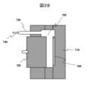
図28はプラスチック成型技術で,図1に示した導光板の両面に回折格子を一体成型する方法の摸式図である。ナノインプリント法やエッチング等の従来用いられている導光板の作成は半導体加工技術に基づく,表面加工技術である。一方,射出成型法等のプラスチック成型技術は,金型の内部に樹脂を導入して固めることによる立体成型技術であるため,導光板の両面に回折格子を形成することが容易である。 FIG. 28 is a schematic diagram of a method of integrally molding diffraction gratings on both sides of the light guide plate shown in FIG. 1 using plastic molding technology. Conventionally used techniques for producing light guide plates, such as nanoimprinting and etching, are surface processing techniques based on semiconductor processing techniques. On the other hand, plastic molding techniques such as injection molding are three-dimensional molding techniques that involve introducing resin into a mold and solidifying it, making it easy to form diffraction gratings on both sides of the light guide plate.
図中,形成すべき回折格子の表面形状を凹凸反転した形で表面にもつスタンパ700を金型の固定部710に固定する。このような金型を用いて,樹脂流路730から溶融した樹脂740を注入するとともに,金型可動部720を図中の右方向に移動させることにより,圧力を印加することで,樹脂740をキャビティ750の形状に沿った形状にするとともに,冷却過程を経て所望の導光板を作成することが可能である。本方法は一般的なものであって,回折格子が凹凸形状として形成された導光板をプラスチックで作成することができる。
In the figure, a
図29は、本実施例の画像表示装置の構成を示す摸式図である。
この画像表示装置では、プラスチックを導光板100の材料として使用する。図9で説明したように、回折効率の高い入射回折格子では、アスペクト比の高いパターンは作りにくいので、アスペクト比の低くできる反射型の回折格子を入射回折格子101として用いている。反射型の入射回折格子は、導光板100内部に光を反射するので、入射回折格子101は、導光板100の映像光線の入射面(第1面)の反対側の面(第2面)に配置される。
FIG. 29 is a schematic diagram showing the configuration of the image display device of this example.
In this image display device, plastic is used as the material for the
導光板100を複数用いる場合、図10A,図10Bで説明したように、視認される画素位置のずれを小さくするためには、図29のように、光線の入射面(第1面)と反対側(第2面)に光が射出する透過型の光学構成が望ましい。
When using a plurality of
先に述べたように、導光板100としては,1次反射回折が支配的な光をユーザが視認する構成により、低いアスペクト比で視認輝度を高くすることができるので、回折効率を重視した場合、出射回折格子は1次反射回折光が第2面に射出するように、第1面に配置するのがよい。しかし、基板の両面に回折格子を作るのはプロセスが煩雑なので、本実施例では出射回折格子102も同じ面(第2面)に作って、1次透過回折光を第2面に射出する構成にしている。
As mentioned above, the
この場合、視認輝度の点では不利なので、輝度を向上させるための構成が重要である。本実施例では、回折格子に誘電体膜を形成することにより、回折効率を向上させることにした。具体的構成としては、入射回折格子101と出射回折格子102のすくなくとも一つに膜があれば最終的に輝度の向上が期待できる。本実施例では、図6と同様に出射回折格子102にコーティング層103を形成している。また、図27のように入射回折格子101にコーティング層104を形成することも可能である。あるいは、図18のように入射回折格子101と出射回折格子102の両方にコーティング層103,104を形成することも可能である。以上の画像表示素子の構成では、入射回折格子では反射回折効率が、出射回折格子では透過回折効率の向上が必要になる。
In this case, there is a disadvantage in terms of visible brightness, so a configuration for improving brightness is important. In this example, it was decided to improve the diffraction efficiency by forming a dielectric film on the diffraction grating. As a specific configuration, if at least one of the
入射回折格子101の構成例としては、図22Bで説明した多層誘電体膜が波長選択性に優れ有効である。また、出射回折格子102の構成例としては、図3に示した格子状の回折格子は低アスペクト比で高い回折効率を得られる。
As an example of the structure of the
もっとも、画像表示素子の構成は上記に限られず、入射回折格子と出射回折格子の構成も種々の形態が考えられる。その場合でも、入射回折格子と出射回折格子のそれぞれで必要とされる反射回折効率と透過回折効率に応じて、形成する膜の特性をコントロールすることで、回折効率を向上させ輝度を向上することができる。 However, the configuration of the image display element is not limited to the above, and various configurations of the input diffraction grating and the output diffraction grating can be considered. Even in that case, it is possible to improve diffraction efficiency and brightness by controlling the characteristics of the formed film according to the reflection diffraction efficiency and transmission diffraction efficiency required for the input and output diffraction gratings, respectively. I can do it.
図中のプロジェクタ300から出射した画像情報をもつ光は,導光板100a,100bの作用によりユーザの瞳400に届けられ,拡張現実を実現する。各導光板100a,100bでは,形成される回折格子のピッチと深さは,各色に応じて最適化されたものである。
Light carrying image information emitted from the
図中,本実施例の画像表示装置は画像表示素子10,プロジェクタ300,および表示画像制御部2901からなる。また,画像形成の方法としては,例えば、反射型または透過型の空間光変調器と光源とレンズから構成された画像形成装置,有機および無機EL(Electro Luminescence)素子アレイとレンズによる画像形成装置、発光ダイオードアレイとレンズによる画像形成装置,光源と半導体MEMSミラーアレイとレンズを組み合わせた画像形成装置等,広く公知の画像形成装置を用いることができる。
In the figure, the image display device of this embodiment includes an
また,LEDやレーザ光源と光ファイバの先端をMEMS技術やPZT等により共振運動させたものを用いることもできる。これらの中で,最も一般的なものは、反射型または透過型の空間光変調器と光源とレンズから構成された画像形成装置である。ここで、空間光変調装置として、LCOS(Liquid Crystal On Silicon)等の透過型あるいは反射型の液晶表示装置、デジタルマイクロミラーデバイス(DMD)を挙げることができ、光源としては白色光源をRGB分離して用いることも,各色対応のLEDやレーザを用いることもできる。 Furthermore, it is also possible to use an LED or laser light source and the tip of an optical fiber which are made to resonate in resonance using MEMS technology, PZT, or the like. Among these, the most common is an image forming apparatus composed of a reflective or transmissive spatial light modulator, a light source, and a lens. Here, examples of spatial light modulators include transmissive or reflective liquid crystal display devices such as LCOS (Liquid Crystal On Silicon), and digital micromirror devices (DMD), and as light sources, white light sources are separated into RGB. It is also possible to use LEDs and lasers corresponding to each color.
更には、反射型空間光変調装置は、液晶表示装置、及び、光源からの光の一部を反射して液晶表示装置へと導き、且つ、液晶表示装置によって反射された光の一部を通過させてレンズを用いたコリメート光学系へと導く偏光ビームスプリッターから成る構成とすることができる。光源を構成する発光素子として、赤色発光素子、緑色発光素子、青色発光素子、白色発光素子を挙げることができる。画素の数は、画像表示装置に要求される仕様に基づき決定すればよく、画素の数の具体的な値として、上で示した1280x720のほかに,320×240、432×240、640×480、1024×768、1920×1080を例示することができる。 Furthermore, the reflective spatial light modulator reflects a portion of the light from the liquid crystal display device and the light source and guides it to the liquid crystal display device, and also transmits a portion of the light reflected by the liquid crystal display device. It can be configured to include a polarizing beam splitter that guides the beam to a collimating optical system using a lens. Examples of the light emitting elements constituting the light source include red light emitting elements, green light emitting elements, blue light emitting elements, and white light emitting elements. The number of pixels may be determined based on the specifications required for the image display device, and specific values for the number of pixels include 1280x720 shown above, 320x240, 432x240, 640x480. , 1024×768, and 1920×1080.
本実施例の画像表示装置では,プロジェクタ300から出射した映像情報を含む光線が,導光板100a,100bの各入射回折格子に照射されるように,位置決めして,画像表示素子10と一体化されて形成される。
In the image display device of this embodiment, the light beam containing image information emitted from the
また,図示しない表示画像制御部は,プロジェクタ300の動作を制御して,ユーザの瞳400に適宜,画像情報を提供する機能を果たす。
Further, a display image control unit (not shown) functions to control the operation of the
以上説明した実施例では、表面凹凸型の回折格子を有する導光板(画像表示素子)において,例えば出射回折格子としてメッシュ型の回折格子を用い,射出成型法等により導波路と同じ屈折率の材料で一体成型することにより,導光板のプラスチック化を実現し,安全で軽量な導光板を実現することができる。すなわち、メッシュ型回折格子を用いることにより,アスペクト比1以下の表面凹凸で良好な性能を有する導光板を射出成型法で作成可能となり,導光板のプラスチック化による安全性の向上と軽量化を実現することができた。 In the embodiments described above, in a light guide plate (image display element) having a surface uneven diffraction grating, a mesh type diffraction grating is used as an output diffraction grating, and a material having the same refractive index as the waveguide is formed by injection molding or the like. By integrally molding the light guide plate with plastic, it is possible to create a safe and lightweight light guide plate. In other words, by using a mesh diffraction grating, it is possible to create a light guide plate with good performance with surface irregularities with an aspect ratio of 1 or less using injection molding, and by making the light guide plate plastic, it is possible to improve safety and reduce weight. We were able to.
本実施例では,ユーザに画像情報を提供する場合について示したが,本実施例の画像表示装置は,このほかにユーザや外界の情報を取得するためのタッチセンサ,温度センサ,加速度センサ等の各種センサや,ユーザの目の動きを計測するためのアイ・トラッキング機構を備えることが可能である。 In this example, a case has been described in which image information is provided to the user, but the image display device of this example also has a touch sensor, a temperature sensor, an acceleration sensor, etc. for acquiring information about the user and the outside world. It is possible to include various sensors and an eye tracking mechanism for measuring the user's eye movements.
100:導光板
101:入射回折格子
102:出射回折格子
300:プロジェクタ
100: Light guide plate 101: Input diffraction grating 102: Output diffraction grating 300: Projector
Claims (4)
前記プラスチック基板表面に一体形成され、入射した映像光を回折する入射回折格子と、
前記プラスチック基板表面に一体形成され、前記映像光を出射する出射回折格子と、
前記入射回折格子の凹凸パターンの周期高さをHとしたとき、膜厚d1の第1の誘電体材料と膜厚d2の第2の誘電体材料は交互にN(Nは自然数)周期積層された積層膜を有し、0.7H<d1+d2<1.3Hであり、かつ(d1+d2)×Nが1000nm以下の多層コーティング層と、を備え、
前記多層コーティング層は前記入射回折格子上に設けられ、
前記積層膜の前記プラスチック基板から遠い方の表面は,前記凹凸パターンの形状が反映されていることを特徴とする画像表示素子。 a plastic substrate,
an incident diffraction grating that is integrally formed on the surface of the plastic substrate and diffracts incident image light;
an output diffraction grating that is integrally formed on the surface of the plastic substrate and that outputs the image light;
When the periodic height of the concavo-convex pattern of the incident diffraction grating is H, the first dielectric material having a thickness d1 and the second dielectric material having a thickness d2 are alternately laminated with N (N is a natural number) periods. 0.7H<d1+d2<1.3H, and a multilayer coating layer in which (d1+d2)×N is 1000 nm or less,
the multilayer coating layer is provided on the incident diffraction grating;
An image display element characterized in that the surface of the laminated film farther from the plastic substrate reflects the shape of the concavo-convex pattern.
前記プラスチック基板表面に一体形成され、入射した映像光を回折する入射回折格子と、
前記プラスチック基板表面に一体形成され、前記映像光を出射する出射回折格子と、
前記入射回折格子の凹凸パターンの周期高さをHとしたとき、膜厚d1の第1の誘電体材料と膜厚d2の第2の誘電体材料は交互にN(Nは自然数)周期積層され、d1+d2がほぼHに等しく、かつ(d1+d2)×Nが1000nm以下の多層コーティング層と、を備え、
前記多層コーティング層は前記入射回折格子上に設けられ、
前記第1の誘電体材料の屈折率をn1,厚さd1とし、前記第2の誘電体材料の屈折率をn2,厚さd2としたとき、
n1>n2、かつ、0.7H<d1+d2<1.3Hであり、
前記Hは、
前記入射回折格子が階段状回折格子であって、その高さがM(Mは2以上の自然数)レベル、最大高さがhの場合、
H=(M/M-1)h
前記入射回折格子がブレーズ型回折格子であって、そのブレーズ角がθB、回折格子周期がpの場合、
H=p・tanθB
前記入射回折格子が一般形状の回折格子であって、その平均傾きから得たブレーズ角がθ、回折格子周期がPの場合、
H=P・tanθ
であることを特徴とする画像表示素子。 a plastic substrate,
an incident diffraction grating that is integrally formed on the surface of the plastic substrate and diffracts incident image light;
an output diffraction grating that is integrally formed on the surface of the plastic substrate and that outputs the image light;
When the periodic height of the concavo-convex pattern of the incident diffraction grating is H, the first dielectric material having a thickness d1 and the second dielectric material having a thickness d2 are alternately laminated with N (N is a natural number) periods. , a multilayer coating layer in which d1+d2 is approximately equal to H and (d1+d2)×N is 1000 nm or less,
the multilayer coating layer is provided on the incident diffraction grating;
When the refractive index of the first dielectric material is n1 and the thickness d1, and the refractive index of the second dielectric material is n2 and the thickness d2,
n1>n2 and 0.7H<d1+d2<1.3H,
The above H is
When the incident diffraction grating is a stepped diffraction grating, the height is M levels (M is a natural number of 2 or more) , and the maximum height is h,
H=( M / M -1)h
When the incident diffraction grating is a blazed diffraction grating, the blaze angle is θ B and the grating period is p,
H=p・tanθ B
When the incident diffraction grating is a general-shaped diffraction grating, the blaze angle obtained from its average slope is θ, and the diffraction grating period is P,
H=P・tanθ
An image display element characterized by:
プラスチック基板と、
前記プラスチック基板表面に一体形成され、入射した映像光を回折する入射回折格子と、
前記プラスチック基板表面に一体形成され、前記映像光を出射する出射回折格子と、
前記出射回折格子上に形成された10nm以上1000nm以下、屈折率が1.4以上2.42以下のコーティング層とを有し、
前記入射回折格子と前記出射回折格子が、前記プラスチック基板の第1の面に形成され、
前記プロジェクタは前記第1の面と反対側の第2の面側に設けられ、
前記プラスチック基板の前記第1の面側から映像光を視認できるように構成され、
前記入射回折格子は反射型回折格子であり、該反射型回折格子の上に多層コーティング層を備え、
前記多層コーティング層は、第1の誘電体薄膜と第2の誘電体薄膜を交互に形成した周期構造を有し、
前記第1の誘電体薄膜の屈折率をn1,厚さd1とし、前記第2の誘電体薄膜の屈折率をn2,厚さd2としたとき、
n1>n2、かつ、0.7H<d1+d2<1.3Hであり、
前記Hは、
前記入射回折格子が階段状回折格子であって、その高さがM(Mは2以上の自然数)レベル、最大高さがhの場合、
H=(M/M-1)h
前記入射回折格子がブレーズ型回折格子であって、そのブレーズ角がθB、回折格子周期がpの場合、
H=p・tanθB
前記入射回折格子が一般形状の回折格子であって、その平均傾きから得たブレーズ角がθ、回折格子周期がPの場合、
H=P・tanθ
であることを特徴とする画像表示装置。 A projector that is a light source for forming image light,
a plastic substrate,
an incident diffraction grating that is integrally formed on the surface of the plastic substrate and diffracts incident image light;
an output diffraction grating that is integrally formed on the surface of the plastic substrate and that outputs the image light;
a coating layer formed on the exit diffraction grating with a thickness of 10 nm or more and 1000 nm or less and a refractive index of 1.4 or more and 2.42 or less,
the entrance diffraction grating and the exit diffraction grating are formed on a first surface of the plastic substrate;
The projector is provided on a second surface opposite to the first surface,
configured such that image light can be visually recognized from the first surface side of the plastic substrate,
the incident diffraction grating is a reflection grating, and comprises a multilayer coating layer on the reflection grating;
The multilayer coating layer has a periodic structure in which first dielectric thin films and second dielectric thin films are alternately formed,
When the refractive index of the first dielectric thin film is n1 and the thickness d1, and the refractive index of the second dielectric thin film is n2 and the thickness d2,
n1>n2 and 0.7H<d1+d2<1.3H,
The above H is
When the incident diffraction grating is a stepped diffraction grating, the height is M levels (M is a natural number of 2 or more) , and the maximum height is h,
H=( M / M -1)h
When the incident diffraction grating is a blazed diffraction grating, the blaze angle is θ B and the grating period is p,
H=p・tanθ B
When the incident diffraction grating is a general-shaped diffraction grating, the blaze angle obtained from its average slope is θ, and the diffraction grating period is P,
H=P・tanθ
An image display device characterized by:
プラスチック基板と、
前記プラスチック基板表面に一体形成され、入射した映像光を回折する入射回折格子と、
前記プラスチック基板表面に一体形成され、前記映像光を出射する出射回折格子と、
前記入射回折格子と前記出射回折格子が、前記プラスチック基板の第1の面に形成され、
前記プロジェクタは前記第1の面と反対側の第2の面側に設けられ、
前記プラスチック基板の前記第1の面側から映像光を視認できるように構成され、
前記入射回折格子の凹凸パターンの周期高さをHとしたとき、膜厚d1の第1の誘電体材料と膜厚d2の第2の誘電体材料は交互にN(Nは自然数)周期積層された積層膜を有し、0.7H<d1+d2<1.3Hであり、かつ(d1+d2)×Nが1000nm以下の多層コーティング層と、を備え、
前記多層コーティング層は前記入射回折格子上に設けられ、
前記積層膜の前記プラスチック基板から遠い方の表面は,前記凹凸パターンの形状が反映されていることを特徴とする画像表示装置。 A projector that is a light source for forming image light,
a plastic substrate,
an incident diffraction grating that is integrally formed on the surface of the plastic substrate and diffracts incident image light;
an output diffraction grating that is integrally formed on the surface of the plastic substrate and that outputs the image light;
the entrance diffraction grating and the exit diffraction grating are formed on a first surface of the plastic substrate;
The projector is provided on a second surface opposite to the first surface,
configured such that image light can be visually recognized from the first surface side of the plastic substrate,
When the periodic height of the concavo-convex pattern of the incident diffraction grating is H, the first dielectric material having a thickness d1 and the second dielectric material having a thickness d2 are alternately laminated with N (N is a natural number) periods. 0.7H<d1+d2<1.3H, and a multilayer coating layer in which (d1+d2)×N is 1000 nm or less,
the multilayer coating layer is provided on the incident diffraction grating;
An image display device characterized in that the surface of the laminated film farther from the plastic substrate reflects the shape of the uneven pattern.
Priority Applications (5)
| Application Number | Priority Date | Filing Date | Title |
|---|---|---|---|
| JP2020002825A JP7341907B2 (en) | 2020-01-10 | 2020-01-10 | Image display elements and devices |
| CN202080089119.4A CN114846386B (en) | 2020-01-10 | 2020-10-08 | Image display element and image display device |
| PCT/JP2020/038161 WO2021140717A1 (en) | 2020-01-10 | 2020-10-08 | Image display element and device |
| US17/782,692 US20230010994A1 (en) | 2020-01-10 | 2020-10-08 | Image display element and device |
| TW109136214A TWI753617B (en) | 2020-01-10 | 2020-10-20 | Image Display Components and Devices |
Applications Claiming Priority (1)
| Application Number | Priority Date | Filing Date | Title |
|---|---|---|---|
| JP2020002825A JP7341907B2 (en) | 2020-01-10 | 2020-01-10 | Image display elements and devices |
Publications (3)
| Publication Number | Publication Date |
|---|---|
| JP2021110838A JP2021110838A (en) | 2021-08-02 |
| JP2021110838A5 JP2021110838A5 (en) | 2022-05-09 |
| JP7341907B2 true JP7341907B2 (en) | 2023-09-11 |
Family
ID=76788158
Family Applications (1)
| Application Number | Title | Priority Date | Filing Date |
|---|---|---|---|
| JP2020002825A Active JP7341907B2 (en) | 2020-01-10 | 2020-01-10 | Image display elements and devices |
Country Status (5)
| Country | Link |
|---|---|
| US (1) | US20230010994A1 (en) |
| JP (1) | JP7341907B2 (en) |
| CN (1) | CN114846386B (en) |
| TW (1) | TWI753617B (en) |
| WO (1) | WO2021140717A1 (en) |
Citations (8)
| Publication number | Priority date | Publication date | Assignee | Title |
|---|---|---|---|---|
| US20050112510A1 (en) | 2003-09-10 | 2005-05-26 | Asml Netherlands B.V. | Optical element, lithographic apparatus, method for manufacturing and/or protecting an optical element, device manufacturing method and device manufactured thereby |
| JP2007515689A (en) | 2003-12-23 | 2007-06-14 | オリバ ジョビン イボン エス. アー. エス. | Two-dimensional grating network with alternating multi-layer stacks, its production and spectroscope equipped with these networks |
| US20100277803A1 (en) | 2006-12-14 | 2010-11-04 | Nokia Corporation | Display Device Having Two Operating Modes |
| US20130100362A1 (en) | 2011-10-24 | 2013-04-25 | Google Inc. | Near-to-eye display with diffraction grating that bends and focuses light |
| US20150293357A1 (en) | 2012-10-18 | 2015-10-15 | Lg Electronics Inc. | Optical device |
| JP2017156388A (en) | 2016-02-29 | 2017-09-07 | セイコーエプソン株式会社 | Luminous flux diameter expansion element and image display device |
| US20170307886A1 (en) | 2016-04-25 | 2017-10-26 | Petri Antero Stenberg | Refractive coating for diffractive optical elements |
| WO2020008949A1 (en) | 2018-07-02 | 2020-01-09 | 株式会社日立エルジーデータストレージ | Optical guide plate, optical guide plate module, image display device, and method for manufacturing optical guide plate |
Family Cites Families (17)
| Publication number | Priority date | Publication date | Assignee | Title |
|---|---|---|---|---|
| JPH0588151A (en) * | 1991-09-27 | 1993-04-09 | Matsushita Electric Ind Co Ltd | Liquid crystal panel and production thereof and liquid crystal projection type television |
| JPH0815514A (en) * | 1994-06-24 | 1996-01-19 | Canon Inc | Reflection type diffraction grating |
| JPH10133008A (en) * | 1996-11-01 | 1998-05-22 | Japan Aviation Electron Ind Ltd | Multilayered diffraction grating and its production |
| JP2005115152A (en) * | 2003-10-09 | 2005-04-28 | Sankyo Seiki Mfg Co Ltd | Lens and optical head device |
| CN101995594A (en) * | 2005-08-29 | 2011-03-30 | 松下电器产业株式会社 | Diffractive optical element and method for manufacturing the same, and imaging apparatus using the diffractive optical element |
| US20090225424A1 (en) * | 2005-09-30 | 2009-09-10 | Fabian Zimmer | Micro-optical diffraction grid and process for producing the same |
| JP4630393B2 (en) * | 2008-12-26 | 2011-02-09 | パナソニック株式会社 | Diffraction lens and imaging apparatus using the same |
| CN102236118B (en) * | 2010-05-07 | 2013-10-16 | 同济大学 | Blazed grating with planar structure |
| FI125270B (en) * | 2012-09-20 | 2015-08-14 | Teknologian Tutkimuskeskus Vtt Oy | Optical device with diffractive grating |
| EP3063570B1 (en) * | 2013-10-29 | 2021-03-17 | CSEM Centre Suisse D'electronique Et De Microtechnique SA | Optical grating coupling structure |
| JP2016048315A (en) * | 2014-08-27 | 2016-04-07 | Hoya株式会社 | Chromogenic structure and exterior parts |
| EP3745167A1 (en) * | 2015-04-07 | 2020-12-02 | Magic Leap, Inc. | Diffraction grating and method of manufacture |
| WO2016162606A1 (en) * | 2015-04-08 | 2016-10-13 | Dispelix Oy | Optical see-through display element and device utilizing such element |
| US10025093B2 (en) * | 2016-04-13 | 2018-07-17 | Microsoft Technology Licensing, Llc | Waveguide-based displays with exit pupil expander |
| JP6410906B1 (en) * | 2017-09-26 | 2018-10-24 | デクセリアルズ株式会社 | Polarizing element and optical device |
| TWI767081B (en) * | 2017-10-30 | 2022-06-11 | 美商菲絲博克科技有限公司 | Method and system for fabricating slanted surface-relief structure using chemically assisted reactive ion beam etching |
| US10845596B2 (en) * | 2018-01-23 | 2020-11-24 | Facebook Technologies, Llc | Slanted surface relief grating for rainbow reduction in waveguide display |
-
2020
- 2020-01-10 JP JP2020002825A patent/JP7341907B2/en active Active
- 2020-10-08 WO PCT/JP2020/038161 patent/WO2021140717A1/en active Application Filing
- 2020-10-08 US US17/782,692 patent/US20230010994A1/en active Pending
- 2020-10-08 CN CN202080089119.4A patent/CN114846386B/en active Active
- 2020-10-20 TW TW109136214A patent/TWI753617B/en active
Patent Citations (8)
| Publication number | Priority date | Publication date | Assignee | Title |
|---|---|---|---|---|
| US20050112510A1 (en) | 2003-09-10 | 2005-05-26 | Asml Netherlands B.V. | Optical element, lithographic apparatus, method for manufacturing and/or protecting an optical element, device manufacturing method and device manufactured thereby |
| JP2007515689A (en) | 2003-12-23 | 2007-06-14 | オリバ ジョビン イボン エス. アー. エス. | Two-dimensional grating network with alternating multi-layer stacks, its production and spectroscope equipped with these networks |
| US20100277803A1 (en) | 2006-12-14 | 2010-11-04 | Nokia Corporation | Display Device Having Two Operating Modes |
| US20130100362A1 (en) | 2011-10-24 | 2013-04-25 | Google Inc. | Near-to-eye display with diffraction grating that bends and focuses light |
| US20150293357A1 (en) | 2012-10-18 | 2015-10-15 | Lg Electronics Inc. | Optical device |
| JP2017156388A (en) | 2016-02-29 | 2017-09-07 | セイコーエプソン株式会社 | Luminous flux diameter expansion element and image display device |
| US20170307886A1 (en) | 2016-04-25 | 2017-10-26 | Petri Antero Stenberg | Refractive coating for diffractive optical elements |
| WO2020008949A1 (en) | 2018-07-02 | 2020-01-09 | 株式会社日立エルジーデータストレージ | Optical guide plate, optical guide plate module, image display device, and method for manufacturing optical guide plate |
Also Published As
| Publication number | Publication date |
|---|---|
| TW202127072A (en) | 2021-07-16 |
| JP2021110838A (en) | 2021-08-02 |
| CN114846386A (en) | 2022-08-02 |
| WO2021140717A1 (en) | 2021-07-15 |
| TWI753617B (en) | 2022-01-21 |
| CN114846386B (en) | 2024-04-02 |
| US20230010994A1 (en) | 2023-01-12 |
Similar Documents
| Publication | Publication Date | Title |
|---|---|---|
| US20200012031A1 (en) | Image display device | |
| WO2020255482A1 (en) | Light guide plate, production method for same, light guide plate module, and image display device | |
| JP4655771B2 (en) | Optical device and virtual image display device | |
| US11561393B2 (en) | Light guide plate and image display device | |
| WO2020008949A1 (en) | Optical guide plate, optical guide plate module, image display device, and method for manufacturing optical guide plate | |
| JP7341906B2 (en) | Image display element, image display device, and image display method | |
| JP7341907B2 (en) | Image display elements and devices | |
| JP7465826B2 (en) | Light guide plate, light guide plate module and image display device | |
| TW202117374A (en) | Holographic waveguide |
Legal Events
| Date | Code | Title | Description |
|---|---|---|---|
| A521 | Request for written amendment filed |
Free format text: JAPANESE INTERMEDIATE CODE: A523 Effective date: 20220425 |
|
| A621 | Written request for application examination |
Free format text: JAPANESE INTERMEDIATE CODE: A621 Effective date: 20220425 |
|
| A131 | Notification of reasons for refusal |
Free format text: JAPANESE INTERMEDIATE CODE: A131 Effective date: 20230509 |
|
| A521 | Request for written amendment filed |
Free format text: JAPANESE INTERMEDIATE CODE: A523 Effective date: 20230616 |
|
| TRDD | Decision of grant or rejection written | ||
| A01 | Written decision to grant a patent or to grant a registration (utility model) |
Free format text: JAPANESE INTERMEDIATE CODE: A01 Effective date: 20230829 |
|
| A61 | First payment of annual fees (during grant procedure) |
Free format text: JAPANESE INTERMEDIATE CODE: A61 Effective date: 20230830 |
|
| R150 | Certificate of patent or registration of utility model |
Ref document number: 7341907 Country of ref document: JP Free format text: JAPANESE INTERMEDIATE CODE: R150 |