JP7337148B2 - Pressure sensing device and stylus - Google Patents
Pressure sensing device and stylus Download PDFInfo
- Publication number
- JP7337148B2 JP7337148B2 JP2021511106A JP2021511106A JP7337148B2 JP 7337148 B2 JP7337148 B2 JP 7337148B2 JP 2021511106 A JP2021511106 A JP 2021511106A JP 2021511106 A JP2021511106 A JP 2021511106A JP 7337148 B2 JP7337148 B2 JP 7337148B2
- Authority
- JP
- Japan
- Prior art keywords
- strain
- sensitive material
- plate
- sensing device
- pressure sensing
- Prior art date
- Legal status (The legal status is an assumption and is not a legal conclusion. Google has not performed a legal analysis and makes no representation as to the accuracy of the status listed.)
- Active
Links
Images


Classifications
-
- G—PHYSICS
- G01—MEASURING; TESTING
- G01L—MEASURING FORCE, STRESS, TORQUE, WORK, MECHANICAL POWER, MECHANICAL EFFICIENCY, OR FLUID PRESSURE
- G01L5/00—Apparatus for, or methods of, measuring force, work, mechanical power, or torque, specially adapted for specific purposes
- G01L5/16—Apparatus for, or methods of, measuring force, work, mechanical power, or torque, specially adapted for specific purposes for measuring several components of force
- G01L5/161—Apparatus for, or methods of, measuring force, work, mechanical power, or torque, specially adapted for specific purposes for measuring several components of force using variations in ohmic resistance
- G01L5/1627—Apparatus for, or methods of, measuring force, work, mechanical power, or torque, specially adapted for specific purposes for measuring several components of force using variations in ohmic resistance of strain gauges
-
- G—PHYSICS
- G06—COMPUTING; CALCULATING OR COUNTING
- G06F—ELECTRIC DIGITAL DATA PROCESSING
- G06F3/00—Input arrangements for transferring data to be processed into a form capable of being handled by the computer; Output arrangements for transferring data from processing unit to output unit, e.g. interface arrangements
- G06F3/01—Input arrangements or combined input and output arrangements for interaction between user and computer
- G06F3/03—Arrangements for converting the position or the displacement of a member into a coded form
- G06F3/033—Pointing devices displaced or positioned by the user, e.g. mice, trackballs, pens or joysticks; Accessories therefor
- G06F3/0354—Pointing devices displaced or positioned by the user, e.g. mice, trackballs, pens or joysticks; Accessories therefor with detection of 2D relative movements between the device, or an operating part thereof, and a plane or surface, e.g. 2D mice, trackballs, pens or pucks
- G06F3/03545—Pens or stylus
-
- G—PHYSICS
- G01—MEASURING; TESTING
- G01L—MEASURING FORCE, STRESS, TORQUE, WORK, MECHANICAL POWER, MECHANICAL EFFICIENCY, OR FLUID PRESSURE
- G01L1/00—Measuring force or stress, in general
- G01L1/20—Measuring force or stress, in general by measuring variations in ohmic resistance of solid materials or of electrically-conductive fluids; by making use of electrokinetic cells, i.e. liquid-containing cells wherein an electrical potential is produced or varied upon the application of stress
- G01L1/22—Measuring force or stress, in general by measuring variations in ohmic resistance of solid materials or of electrically-conductive fluids; by making use of electrokinetic cells, i.e. liquid-containing cells wherein an electrical potential is produced or varied upon the application of stress using resistance strain gauges
- G01L1/225—Measuring circuits therefor
-
- G—PHYSICS
- G06—COMPUTING; CALCULATING OR COUNTING
- G06F—ELECTRIC DIGITAL DATA PROCESSING
- G06F3/00—Input arrangements for transferring data to be processed into a form capable of being handled by the computer; Output arrangements for transferring data from processing unit to output unit, e.g. interface arrangements
- G06F3/01—Input arrangements or combined input and output arrangements for interaction between user and computer
- G06F3/03—Arrangements for converting the position or the displacement of a member into a coded form
- G06F3/033—Pointing devices displaced or positioned by the user, e.g. mice, trackballs, pens or joysticks; Accessories therefor
- G06F3/038—Control and interface arrangements therefor, e.g. drivers or device-embedded control circuitry
- G06F3/0383—Signal control means within the pointing device
-
- G—PHYSICS
- G06—COMPUTING; CALCULATING OR COUNTING
- G06F—ELECTRIC DIGITAL DATA PROCESSING
- G06F3/00—Input arrangements for transferring data to be processed into a form capable of being handled by the computer; Output arrangements for transferring data from processing unit to output unit, e.g. interface arrangements
- G06F3/01—Input arrangements or combined input and output arrangements for interaction between user and computer
- G06F3/03—Arrangements for converting the position or the displacement of a member into a coded form
- G06F3/041—Digitisers, e.g. for touch screens or touch pads, characterised by the transducing means
- G06F3/046—Digitisers, e.g. for touch screens or touch pads, characterised by the transducing means by electromagnetic means
Description
この発明は、受けた力に応じて生じるひずみなどの変位を検出することに基づいて、前記受けた力を検出する圧力センシングデバイスに関する。また、この発明は、圧力センシングデバイスを用いて、例えば芯体に対して印加される力を検出するスタイラスに関する。 TECHNICAL FIELD The present invention relates to a pressure sensing device that detects a received force based on detecting displacement such as strain that occurs in response to the received force. The invention also relates to a stylus that uses a pressure sensing device to detect force applied to, for example, a core.
スタイラス(電子ペン)においては、位置検出センサの入力面に対する接触や、接触時の圧力(筆圧)筆圧を検出するための筆圧検出部を有するものが多く、ひずみゲージを用いることも提案されている(特許文献1及び特許文献2参照)。ひずみゲージは、ひずみ受感材の電気抵抗が、当該ひずみ受感材のひずみ(弾性ひずみだけでなく塑性ひずみを含む)によって変化する現象を利用したものである。
Many styluses (electronic pens) have a writing pressure detection unit for detecting contact with the input surface of the position detection sensor and the pressure (writing pressure) at the time of contact, and the use of a strain gauge is also proposed. (See
ひずみゲージを用いた圧力検出部材としては、印加された力(圧力)の互いに直交する3軸方向(X軸方向、Y軸方向、Z軸方向)の力成分を検出する、いわゆる3軸圧力検出部材も提案されている(特許文献3及び特許文献4参照)。この3軸圧力検出部材を、スタイラスに用いた場合、スタイラスの軸心方向の圧力(筆圧)のみならず、スタイラスが所定の角度傾いた状態においても、スタイラスのペン先に印加される力を検出することができて、スタイラスの傾き角やスタイラスのペン先の摩擦力なども検出することができて便利である。
As a pressure detection member using a strain gauge, a so-called three-axis pressure detection that detects force components in mutually orthogonal three-axis directions (X-axis direction, Y-axis direction, Z-axis direction) of applied force (pressure) A member has also been proposed (see
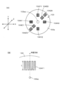
図8は、3軸圧力検出部材の一例を示すものである。この例の圧力検出部材は、起歪部101と、この起歪部101に一体に結合された力受付部102と、起歪部101に取り付けられる圧力センシングデバイス103とからなる。圧力センシングデバイス103は、ひずみゲージからなり、この例では、起歪部101の平面に対して直交する方向をZ軸方向、起歪部101の平面に平行な方向であって、互いに直交する方向をX軸方向及びY軸方向として、力受付部102に印加された力のX,Y,Zの各軸方向の力成分を検出する。
FIG. 8 shows an example of a triaxial pressure detection member. The pressure detecting member of this example comprises a strain-generating
図8(A)は、この例の圧力検出部材の斜視図である。図8(B)は、この例の圧力検出部材の縦断面図(Z軸方向を含む方向の断面図)である。なお、図8(B)では、便宜上、力受付部102は起歪部101の近傍のみ示している。
FIG. 8A is a perspective view of the pressure detection member of this example. FIG. 8B is a longitudinal sectional view (sectional view in a direction including the Z-axis direction) of the pressure detection member of this example. In addition, in FIG. 8B, for the sake of convenience, the
力受付部102は、起歪部101との結合側とは反対側の先端部に印加される力を受け付けて、起歪部101に伝達する機能を備えるもので、この例では、棒状部材とされる。
The force-receiving
起歪部101は、図8(B)に示すように、円筒状のダイヤフラム保持部101bの一方の開口部側に、薄い円板状のダイヤフラム101aが設けられた構造を備えている。そして、起歪部101は、円板状のダイヤフラム101aの中央部において棒状の力受付部102と結合されている。
As shown in FIG. 8B, the
ダイヤフラム101aの、力受付部102との結合側と反対側の面には、圧力センシングデバイス103が接着材により貼り付けられて取り付けられている。
A
この例の圧力センシングデバイス103は、例えば円板形状の絶縁性フィルムシートからなるフレキシブル基板103a上に、受けたひずみ変位に応じて抵抗値を変えるひずみ受感材が、複数個配設されたものからなる。
The
図9(A)に示す例では、ひずみ受感材としては、8個のひずみ受感材104X1,104X2,104Y1,104Y2,104Z1,104Z2,104Z3,104Z4がフレキシブル基板上に配設されている。この例では、ひずみ受感材104X1,104X2,104Y1,104Y2,104Z1,104Z2,104Z3,104Z4の抵抗値は、ひずみが印加されていないときには、互いに等しくなるようにされている。 In the example shown in FIG. 9A, eight strain sensitive materials 104X1, 104X2, 104Y1, 104Y2, 104Z1, 104Z2, 104Z3, and 104Z4 are arranged on a flexible substrate. In this example, the resistance values of the strain sensitive materials 104X1, 104X2, 104Y1, 104Y2, 104Z1, 104Z2, 104Z3 and 104Z4 are made equal to each other when no strain is applied.
ひずみ受感材104X1と104X2とは、力受付部102の軸心方向に直交する方向であるX軸方向のひずみを検知するためのもので、フレキシブル基板103aの中心位置103ac(力の印加位置)を通るX軸方向の直線上において、中心位置103acを挟む両側において、当該中心位置103acから等距離の位置にそれぞれ設けられている。なお、以下の説明で、複数個のひずみ受感材のそれぞれを区別する必要がないときには、ひずみ受感材104と記述することとする。
The strain sensing members 104X1 and 104X2 are for detecting strain in the X-axis direction, which is the direction orthogonal to the axial direction of the
ひずみ受感材104Y1と104Y2とは、力受付部102の軸心方向に直交すると共にX軸方向と直交する方向であるY軸方向のひずみを検知するためのもので、中心位置103acを通るY軸方向の直線上において、中心位置103acを挟む両側において、当該中心位置103acから等距離の位置にそれぞれ設けられている。
The strain sensing members 104Y1 and 104Y2 are for detecting strain in the Y-axis direction, which is perpendicular to the axial direction of the
そして、ひずみ受感材104Z1,104Z2,104Z3,104Z4は、力受付部102の軸心方向であるZ軸方向のひずみを検知するためのものである。図9(A)の例では、中心位置103acを通る直線であって、X軸方向及びY軸方向に対して他のひずみ受感材104X1,104X2,104Y1,104Y2と重ならないように所定角度傾いた直線上において、中心位置103acを挟む両側において、2個ずつのひずみ受感材104Z1,104Z3と、ひずみ受感材104Z2,104Z4とが点対称の位置に設けられている。
The strain sensitive members 104Z1, 104Z2, 104Z3, and 104Z4 are for detecting strain in the Z-axis direction, which is the axial direction of the
従来、複数個のひずみ受感材104のそれぞれは、材料として例えばCu-Ni合金が、温度定数が直線的で安定しているので、ブリッジ回路でひずみ受感材の抵抗値の互いの温度変換分を打ち消せるため温度変化に対して安定であるという点で良く用いられている。なお、ひずみ受感材104としては、半導体の炭素、ケイ素、マグネシウム、Cr薄膜やCr-N薄膜(特許文献5(特許第6084393号公報参照)等も知られている。 Conventionally, each of the plurality of strain sensitive materials 104 is made of, for example, a Cu—Ni alloy as a material, and has a linear and stable temperature constant. It is often used because it is stable against temperature changes because it can cancel the minute. As the strain sensitive material 104, semiconductor carbon, silicon, magnesium, Cr thin films, Cr—N thin films (see Patent Document 5 (Japanese Patent No. 6084393)), etc. are also known.
ひずみ受感材104が、例えばCu-Ni合金からなる場合には、その金属細線や金属箔を、図9(B)の拡大図に示すように、半径方向(ひずみの発生方向)に設定された長さLでジグザグ状に折り曲げて半径方向に直交する方向(円周方向)に配設したものとして構成されている。図9(B)では、ひずみ受感材104Y1の例を示しているが、他のひずみ受感材104X1,104X2,104Y2,104Z1,104Z2,104Z3,104Z4も同様である。
When the strain sensitive material 104 is made of, for example, a Cu—Ni alloy, the fine metal wire or metal foil is set in the radial direction (the direction in which strain occurs) as shown in the enlarged view of FIG. 9(B). It is configured such that it is bent in a zigzag shape with a length L and arranged in a direction perpendicular to the radial direction (circumferential direction). FIG. 9B shows an example of the strain sensitive material 104Y1, but the other strain sensitive materials 104X1, 104X2,
ところで、最近のスタイラスは細型化の要請が大きくなっており、このため、上述した筆圧や傾きを検出する目的で用いられる圧力センシングデバイスについても、更なる小型化の要請が大きくなっている。しかしながら、図8及び図9を用いて説明した圧力センシングデバイス103の構造では、その外周部に引き回し配線エリアや接続端子が配設されており、外周部に配設された引き回し配線エリアや接続端子が小型化を阻害している。
By the way, recent styluses are increasingly required to be slimmer, and for this reason, pressure sensing devices used for the purpose of detecting pen pressure and inclination described above are also being required to be further miniaturized. However, in the structure of the
この発明は、以上の問題点を解決することができるようにした圧力センシングデバイス及び当該圧力センシングデバイスを搭載するスタイラスを提供することを目的とする。 SUMMARY OF THE INVENTION An object of the present invention is to provide a pressure sensing device and a stylus equipped with the pressure sensing device that can solve the above problems.
上記の課題を解決するために、
ペン形状を有し、筐体の一方の端部から突出した先端部と、所定の回路を備えたスタイラスに収納されて、前記先端部に印加された力をセンスするとともに前記スタイラスに収納されて前記所定の回路と電気的に接続される圧力センシングデバイスであって、
板状部材と、前記板状部材に配置された複数のひずみ受感材と、前記所定の回路と電気的に接続するための接続用電極とを備えており、
前記板状部材は、前記先端部に印加された力が伝達される面部を備えており、
前記複数のひずみ受感材は、少なくとも前記板状部材の前記面部に伝達される力の印加部の中心から第1の距離離れて配置された第1のひずみ受感材と、前記中心から前記第1の距離よりも大きな第2の距離離れて配置された第2のひずみ受感材とから構成されており、前記第1のひずみ受感材と前記第2のひずみ受感材とを互いに接続する導電パターンとともに、前記板状部材の少なくとも一方の面部において成膜されて形成されて、前記板状部材の前記面部に伝達された力に応じて前記板状部材に生じるひずみが感知されるように構成されており、
前記接続用電極は、前記複数のひずみ受感材と電気的に接続されているとともに前記スタイラスに収納された前記所定の回路との電気的な接続は圧着にて行われるように構成されていることを特徴とする圧力センシングデバイスを提供する。In order to solve the above problems,
It has a pen shape and is housed in a stylus having a tip protruding from one end of a housing and a predetermined circuit to sense a force applied to the tip and is housed in the stylus. A pressure sensing device electrically connected to the predetermined circuit,
A plate-shaped member, a plurality of strain sensitive materials arranged on the plate-shaped member, and a connection electrode for electrically connecting to the predetermined circuit,
The plate-shaped member has a surface portion to which the force applied to the tip portion is transmitted,
The plurality of strain sensitive materials include a first strain sensitive material arranged at least a first distance away from the center of the force applying portion that is transmitted to the surface portion of the plate-shaped member; and a second strain sensitive material spaced apart by a second distance greater than the first distance, wherein the first strain sensitive material and the second strain sensitive material are separated from each other. A film is formed on at least one surface portion of the plate-like member together with the conductive pattern to be connected, and strain generated in the plate-like member according to the force transmitted to the surface portion of the plate-like member is sensed. is configured as
The connection electrodes are electrically connected to the plurality of strain sensitive materials and are configured to be electrically connected to the predetermined circuit housed in the stylus by crimping. To provide a pressure sensing device characterized by:
また、
ペン形状を有し、筐体の一方の端部から突出した先端部と、前記先端部に印加された力をセンスする圧力センシングデバイスと、前記圧力センシングデバイスに電気的に接続された所定の回路を備えたスタイラスであって、
前記圧力センシングデバイスは、板状部材と、前記板状部材に配置された複数のひずみ受感材と、前記所定の回路と電気的に接続するための接続用電極を備えており、
前記板状部材は、前記先端部に印加された力が伝達される面部を備えており、
前記複数のひずみ受感材は、少なくとも前記板状部材の前記面部に伝達される力の印加部の中心から第1の距離離れて配置された第1のひずみ受感材と、前記中心から前記第1の距離よりも大きな第2の距離離れて配置された第2のひずみ受感材とから構成されており、前記第1のひずみ受感材と前記第2のひずみ受感材とを互いに接続する導電パターンとともに、前記板状部材の少なくとも一方の面部において成膜されて形成されて、前記板状部材の前記面部に伝達された力に応じて前記板状部材に生じるひずみが感知されるように構成されており、
前記接続用電極は、前記複数のひずみ受感材と電気的に接続されているとともに前記スタイラスに収納された前記所定の回路との電気的な接続が前記スタイラスの軸心方向に沿って圧着にて行われるように構成されていることを特徴とするスタイラスを提供する。Also,
A pen-shaped tip protruding from one end of a housing, a pressure sensing device for sensing force applied to the tip, and a predetermined circuit electrically connected to the pressure sensing device. A stylus comprising
The pressure sensing device includes a plate-shaped member, a plurality of strain sensitive materials arranged on the plate-shaped member, and a connection electrode for electrically connecting to the predetermined circuit,
The plate-shaped member has a surface portion to which the force applied to the tip portion is transmitted,
The plurality of strain sensitive materials include a first strain sensitive material arranged at least a first distance away from the center of the force applying portion that is transmitted to the surface portion of the plate-shaped member; and a second strain sensitive material spaced apart by a second distance greater than the first distance, wherein the first strain sensitive material and the second strain sensitive material are separated from each other. A film is formed on at least one surface portion of the plate-like member together with the conductive pattern to be connected, and strain generated in the plate-like member according to the force transmitted to the surface portion of the plate-like member is sensed. is configured as
The connection electrodes are electrically connected to the plurality of strain sensitive materials and electrically connected to the predetermined circuit housed in the stylus by crimping along the axial direction of the stylus. To provide a stylus characterized in that it is configured to:
上記の構成の圧力センシングデバイスにおいては、ひずみ受感材は、板状部材の面部に伝達される力の印加部を中心から第1の距離離れて配置された第1のひずみ受感材と、前記中心から前記第1の距離よりも大きな第2の距離離れて配置された第2のひずみ受感材とから構成されている。そして、ひずみ受感材は、第1のひずみ受感材と第2のひずみ受感材とを互いに接続する導電パターンとともに、板状部材の面部において成膜されて形成されている。 In the pressure sensing device having the above configuration, the strain sensitive material includes a first strain sensitive material arranged at a first distance from the center of the force application portion to be transmitted to the surface portion of the plate-shaped member; and a second strain sensitive material positioned a second distance from said center that is greater than said first distance. The strain sensitive material is formed by depositing a film on the surface portion of the plate-like member together with the conductive pattern that connects the first strain sensitive material and the second strain sensitive material.
そして、接続用電極は、複数のひずみ受感材と電気的に接続されているとともにスタイラスに収納された所定の回路との電気的な接続がスタイラスの軸心方向に沿って圧着にて行われるように構成されている。したがって、接続用電極とスタイラスに収納された所定の回路との接続が容易となる。 The connection electrodes are electrically connected to the plurality of strain sensitive materials and electrically connected to a predetermined circuit housed in the stylus by crimping along the axial direction of the stylus. is configured as Therefore, connection between the connection electrode and a predetermined circuit housed in the stylus is facilitated.
以下、この発明による圧力センシングデバイスの実施形態及びスタイラスの実施形態を、図を参照しながら説明する。以下に説明する実施形態のスタイラスは電磁誘導方式のもので、位置検出装置の位置検出用センサとの間で電磁誘導方式で信号の授受を行なうことで、位置検出装置はスタイラスによる指示位置を検出する。 Embodiments of a pressure sensing device and a stylus according to the present invention will be described below with reference to the drawings. The stylus used in the embodiments described below is of the electromagnetic induction type, and the position detection device detects the position indicated by the stylus by transmitting and receiving signals with the position detection sensor of the position detection device by the electromagnetic induction method. do.
<スタイラスの実施形態の説明>
図1は、この発明の実施形態の圧力センシングデバイス1を、筆圧検出や傾き検出用等として備える実施形態のスタイラス2の構造例を示す図であり、図1(A)は、スタイラス2の外観を示す図、図1(B)は、スタイラス2のペン先側の部分の断面図である。<Description of Embodiment of Stylus>
FIGS. 1A and 1B are diagrams showing a structural example of a
図1(A)に示すように、この実施形態のスタイラス2は、細長形状の筒状の筐体201の軸心方向の一方の開口側がペン先側とされ、他方の開口側が後端側とされる。筐体201の軸心方向の後端側は、後端キャップ部材202により閉塞されている。筐体201は、この例では、SUSで構成されている。筐体201は、樹脂で構成されてもよい。
As shown in FIG. 1A, in the
この実施形態のスタイラス2の筒状の筐体201のペン先側には、図1(B)に示すように、位置検出センサと電磁誘導結合するための共振回路を構成するコイル21が巻回される磁性体コア、この例ではフェライトコア22が配設されると共に、圧力センシングデバイス1が、筐体201の中空部201a内に固定されて配設される。
As shown in FIG. 1B, a
この実施形態のスタイラスでは、筐体201のペン先側の開口には、ペン先側部材203が取り付けられる。この例では、ペン先側部材203は、円筒形状の筒状体のコイルケース203Aと、先細形状の筒状体からなるフロントキャップ203Bとで構成されている。コイルケース203Aは、非磁性材料、この例では、樹脂で構成されている。また、フロントキャップ203Bも、この例では、樹脂で構成されている。そして、コイルケース203Aとフロントキャップ203Bとが、図1(B)に示すように互いに軸心方向に螺合されることで、コイル21が巻回されたフェライトコア22の収納空間が形成される。
In the stylus of this embodiment, a pen
このペン先側部材203は、コイルケース203Aが、筐体201に螺合されることで筐体201に取り付けられる。図1(B)に示すように、コイル21が巻回されたフェライトコア22は、その軸心方向の両端に第1の緩衝部材23及び第2の緩衝部材24が取り付けられて、ペン先側部材203の収納空間に収納される。第1の緩衝部材23及び第2の緩衝部材24は、弾性部材、例えば弾性ゴムで構成されている。
The pen
フェライトコア22には、棒状の芯体31が挿通される軸心方向の貫通孔22aが、その中心位置に形成されている。芯体31は、硬質材料、この例では、SUSで構成されており、その軸心方向の一端31a側が、フロントキャップ203Bの開口203Baから突出するようにされ、その突出する一端31aには、この例では、樹脂で構成されるペン先部材204が圧入嵌合されて取り付けられている。
The
芯体31のペン先部材204が取り付けられた一端31a側とは反対側の他端31b側は、後述するようにして圧力センシングデバイス1と結合されている。したがって、この例では、芯体31は、ペン先部材204に印加される力を受け付ける力受付部を構成し、受け付けた力を圧力センシングデバイス1に伝達する機能を備える。
The
この実施形態の圧力センシングデバイス1は、後述する図2及び図3に示すように、円板状の板状部材10の一方の面部10aに、複数個のひずみ受感材11がジグザグ状に配設されると共に、それら複数個のひずみ受感材11と導電パターン12とからなる回路(ブリッジ回路)が配設されたものである。
In the
圧力センシングデバイス1は、図1(B)に示すように、その一方の面部10aの面方向が筐体201の軸心方向に直交する方向に向く状態で、筐体201の中空部201a内に取り付けられて、筐体201に対して軸心方向に移動不可及び圧力センシングデバイス1の周方向に移動不可の状態で固定される。
As shown in FIG. 1B, the
図1(B)の例では、筐体201の中空部201aには、圧力センシングデバイス1の板状部材10の径よりも内側に更に張り出すリング状突部201bが形成されている。そして、圧力センシングデバイス1が、後端側から筐体201の中空部201a内に挿入され、このリング状突部201bに対して、圧力センシングデバイス1の板状部材10の面部10aとは反対側の面部10bの周縁部が当接するようにされる。
In the example of FIG. 1B, a
そして、図1(B)に示すように、圧力センシングデバイス1の板状部材10の一方の面部10a側の周縁部に対してリング状のワッシャー部材32が配設された後、筒状のセンサホルダー33が、筐体201の中空部201aの内壁面に形成されたねじ部201cにねじ込まれる。筒状のセンサホルダー33の外周側面部には、筐体201のねじ部201cと螺合するねじ部33aが形成されている。
Then, as shown in FIG. 1B, after a ring-shaped
センサホルダー33の筐体201に対する当該ねじ込みにより、圧力センシングデバイス1の板状部材10の周縁部が、筐体201のリング状突部201bと、センサホルダー33の先端のリング状端面との間で、ワッシャー部材32を介して挟持されて、圧力センシングデバイス1は、筐体201の中空部201a内において軸心方向に移動不可で、且つ、周方向にも回動不能の状態で固定される。
By screwing the
そして、図1(B)に示すように、芯体31の他端31b側が、圧力センシングデバイス1の板状部材10の面部10bの中央部に当接されている状態で、結合用ネジ34が、板状部材10の一方の面部10aからねじ込まれることで、板状部材10の面部10bの中央部に、芯体31が結合される。
Then, as shown in FIG. 1B, the
この場合に、図1(B)に示すように、結合用ネジ34のネジ頭34aと、板状部材10の一方の面部10aとの間には、ワッシャー部材35と、当該面部10aに形成されている圧力センシングデバイス1の回路部の端子との電気的な接続のためのフレキシブル基板36が挟持される状態とされている。すなわち、フレキシブル基板36は、結合用ネジ34による圧力センシングデバイス1の板状部材10と芯体31との結合時に、ワッシャー部材35により板状部材10の面部10aに形成されている回路部の端子と圧着されて、電気的な接続がなされている。なお、圧力センシングデバイス1の板状部材10の中心部には、図2及び図3に示すように、結合用ネジ34の径と同径の貫通孔10cが形成されている。
In this case, as shown in FIG. 1B, between the
フレキシブル基板36の圧力センシングデバイス1との結合側とは反対側は、図1(B)に示すように、筐体201の中空部201a内に設けられている基板ホルダー25に保持されているプリント基板26の導電パターンに半田付け等により電気的に接続されている。なお、図示は省略するが、フェライトコア22に巻回されているコイル21の両端は、プリント基板26上に設けられているキャパシタの両端に電気的に接続され、このコイル21とキャパシタとにより、位置検出センサと電磁誘導結合するための共振回路が構成されている。
The side of the
この実施形態のスタイラス2は、以上のように構成されているので、位置検出装置の位置検出センサの入力面に対してスタイラス2のペン先部材204が接触して、当該ペン先部材204を通じて芯体31に印加される力に応じて、圧力センシングデバイス1の板状部材10がひずみ変形をする。
Since the
圧力センシングデバイス1の一方の面部10aに配設されたひずみ受感材では、そのひずみ変形に応じて抵抗値変化を生じるので、当該面部10aに形成されている回路部(ブリッジ回路)の端子には、印加された力に応じた出力電圧が得られる。
The strain-sensitive material provided on one
プリント基板26には、この実施形態では、芯体31の軸心方向に印加される力成分を、ペン先部材204に印加される筆圧として検出すると共に、芯体31の軸心方向に直交する方向に印加される力成分から、位置検出センサの入力面に対するスタイラス2の傾き角を検出するペン状態検出回路が設けられている。そして、ペン状態検出回路は、フレキシブル基板36を通じて送られてくる圧力センシングデバイス1の出力電圧に基づいて、前記筆圧及び前記傾きを検出する。なお、ペン状態検出回路は、圧力センシングデバイス1の出力電圧に基づいて、スタイラス2のペン先部材204と、位置検出センサの入力面との間の摩擦力をも検出するように構成することもできる。
In this embodiment, the printed
<圧力センシングデバイスの実施形態の説明>
図2及び図3は、この発明の実施形態の圧力センシングデバイス1の構成例を説明するための図である。この例の圧力センシングデバイス1は、前述したように、弾性を有する絶縁性部材からなる板状部材10の一方の面部10aに、複数個のひずみ受感材11が配設されて形成されている。図2は、この実施形態の圧力センシングデバイス1の板状部材10の一方の面部10aに配設される複数のひずみ受感材11の配設位置と、印加された力に応じて板状部材10に発生するひずみとの関係を示している。図3(A)に示すように、板状部材10の一方の面部10aには、複数のひずみ受感材11と共に、それらを電気的に接続するための導電パターン12も形成されるが、図2(A)では、その導電パターン12は省略してある。<Description of Embodiment of Pressure Sensing Device>
2 and 3 are diagrams for explaining a configuration example of the
図2(A)及び図3(A)は、圧力センシングデバイス1を、その板状部材10の一方の面部10aに対して直交する方向であって、当該一方の面部10a側から見た図を示している。また、図3(B)は、圧力センシングデバイス1を、板状部材10の面部に平行な方向から見た側面図である。この図3(B)に示すように、この例では、板状部材10は、一定の厚さdを有する円板で構成されている。
2(A) and 3(A) are views of the
この実施形態の圧力センシングデバイス1では、板状部材10は、弾性を有する材料からなる板例えば金属板、この例では、SUSで構成されている。この例では、板状部材10の一方の面部10a側に絶縁層(図示は省略)が設けられて絶縁性部材とされる。そして、板状部材10の一方の面部10a側の絶縁層上に、ひずみ受感材11及び導電パターン12が成膜されて形成されることで、この実施形態ではブリッジ回路が形成されて、圧力センシングデバイス1が形成される。この実施形態の圧力センシングデバイス1では、従来のようにフレキシブル基板にひずみ受感材を配設したものを、ダイヤフラムを構成する起歪体に接着材により接着する構成ではないので、従来のような接着材の影響によるひずみ受感特性の経時変化(クリープ)やばらつきなどの不具合を回避することができる。
In the
この例では、以上のように、圧力センシングデバイス1の板状部材10は、その周縁部10Eが筐体201のリング状突部とセンサホルダー33との間で挟持されて軸心方向及び周方向に移動不可の状態で固定されると共に、その中心部において芯体31が結合用ネジ34によりネジ止めされて結合されるので、図1(B)に示すように、結合用ネジ34の頭部34aの周縁の位置と、センサホルダー33の内径の位置との間の幅Wのリング状領域RGが、芯体31のペン先部材204に印加される力に応じて弾性ひずみを生じることが可能である領域となる。
In this example, as described above, the plate-shaped
すなわち、結合用ネジ34の頭部34aの半径をri、センサホルダー33の内径(リング状ワッシャー部材32の内径と同じ)をroとすると、図2(A)に示すように、圧力センシングデバイス1の板状部材10において、その中心位置Ocを中心とする半径rが、ri<r<roの範囲であるリング状領域RGが、芯体31を通じて伝達される力に対応して弾性ひずみが発生する領域となる。
2A, the
図2(A)及び図3(A)に示すように、この実施形態の圧力センシングデバイス1においては、板状部材10の一方の面部10aの、幅Wのリング状領域RGに、ひずみ受感材11が複数個設けられる。
As shown in FIGS. 2A and 3A, in the
ところで、この例の圧力センシングデバイス1の板状部材10は、一定の厚さdを有する円板形状であって、その周縁部10Eで固定されると共に、その中心位置Oc(図2(A)参照)に、芯体31を通じて力が印加される。
By the way, the plate-
ここで、板状部材10の幅Wのリング状領域RGの幅方向(板状部材10の半径方向)を、板状部材10の中心位置Ocを中心とした半径ri~半径r1の範囲の内側リング状領域RG1と、半径r1~半径r2の範囲の中間リング状領域RG0と、半径r2~半径r0の範囲の外側リング状領域RG2とに3分割する。内側リング状領域RG1は、第1のリング状領域の例を構成し、外側リング状領域RG2は、第2のリング状領域の例を構成する。
Here, the width direction of the ring-shaped region RG having the width W of the plate-shaped member 10 (the radial direction of the plate-shaped member 10) is set inside the range of the radius ri to the radius r1 around the center position Oc of the plate-shaped
このように板状部材10の半径方向を領域分割すると、リング状領域RGの内側リング状領域RG1と外側リング状領域RG2とでは、芯体31のペン先部材204に力が印加されたときには、互いに逆向きの大きなひずみが生じる。そして、中間リング状領域RG0は、印加された力に応じて発生するひずみが逆向きに変化する遷移領域であるため、発生するひずみは小さくなり、半径方向のその中央部では殆どひずみが生じない。
When the radial direction of the plate-shaped
すなわち、圧力センシングデバイス1の板状部材10が、力受付部31を介して面部10aに直交する方向の力(Z軸方向の力)を受けると、板状部材10は、図2(B)に示すように、下に突となるように弾性変形する。この場合に、Z軸方向の力以外の力が零であるときには、板状部材10においては、中心位置Ocから放射方向における同じ半径位置においては、全周に亘って等しいひずみを生じる。そして、そのひずみは、印加された力の大きさに応じたものとなると共に、図2(B)に示すように、内側リング状領域RG1では、伸長ひずみとなり、また、外側リング状領域RG2では、収縮ひずみとなって、互いに逆方向のひずみが生じる。そして、中間リング状領域RG0では、ひずみは比較的小さいものとなる。
That is, when the plate-
したがって、内側リング状領域RG1と外側リング状領域RG2とのひずみの大きい位置に合わせてひずみ受感材11をそれぞれ設けて、内側リング状領域RG1での伸長ひずみと、外側リング状領域RG2での収縮ひずみとをそれぞれ検知することで、Z軸方向の力を検出することができる。すなわち、内側リング状領域RG1に設けたひずみ受感材11と外側リング状領域RG2に設けたひずみ受感材と、互いに逆方向(増加方向と減少方向)に抵抗値が変化するので、その抵抗値の変化分に基づいて、圧力センシングデバイス1に印加されるZ軸方向の力を検出することができる。
Therefore, the strain-
また、力受付部の例としての芯体31を介して圧力センシングデバイス1の板状部材10の面部10aに平行する方向の力(X軸方向またはY軸方向の力)を受けると、板状部材10は、図2(C)に示すように、板状部材10の中心位置Ocを中心として非対称に波打つようなひずみ変形をする。そして、そのひずみ変形の度合は、印加された力の大きさに応じたものとなると共に、図2(C)に示すように、板状部材10では、中心位置Ocを中心として互いに逆向きのひずみが生じる。
Further, when a force in a direction parallel to the
すなわち、図2(C)に示すように、力受付部の例としての芯体31に印加される力の方向から見て、中心位置Ocよりも手前側においては、内側リング状領域RG1では収縮ひずみが生じ、また、外側リング状領域RG2では伸長ひずみが生じる。また、力受付部の例としての芯体31に印加される力の方向から見て、中心位置Ocよりも後ろ側においては、内側リング状領域RG1では伸長ひずみが生じ、また、外側の外側リング状領域RG2では収縮ひずみが生じる。そして、中間リング状領域RG0では、ひずみは比較的小さいものとなる。
That is, as shown in FIG. 2C, when viewed from the direction of the force applied to the
したがって、内側リング状領域RG1に配設されたひずみ受感材11のひずみに応じた抵抗値の変化と、外側リング状領域RG2に配設されたひずみ受感材11のひずみに応じた抵抗値の変化とから、X軸方向又はY軸方向の力成分を検出することができる。そして、この場合に、中心位置Ocよりも手前側の内側リング状領域RG1及び外側リング状領域RG2と、後ろ側の内側リング状領域RG1及び外側リング状領域RG2とでは、発生するひずみの態様が逆向きであることから、中心位置Ocよりも手前側と後ろ側とのそれぞれにおいてひずみ受感材11で検出したひずみ検出出力の差分を取ることで、X軸方向又はY軸方向の力成分の検出出力として、2倍の大きさの検出出力が得られる。
Therefore, the change in the resistance value according to the strain of the strain
この実施形態の圧力センシングデバイス1の板状部材10では、以上のようなひずみ発生態様となることを踏まえて、圧力センシングデバイス1の板状部材10上に、以下に説明するように、ひずみ受感材11を配設することで、3軸圧力センシングデバイスを構成するようにする。
In the plate-shaped
この実施形態においては、圧力センシングデバイス1の板状部材10の面部10aに直交する方向に印加される力をZ軸方向の力として受けて、その大きさを検出する。また、この実施形態においては、圧力センシングデバイス1の板状部材10の面部10aに面方向に平行な方向に印加される力であって、互いに直交する方向の力を、X軸方向及びY軸方向の力として受けて、その大きさを検出する。
In this embodiment, the force applied in the direction orthogonal to the
そこで、この実施形態の圧力センシングデバイス1においては、3軸圧力センシングデバイスとするために、図2(A)及び図3(A)において点線で分割して示すように、円板からなる板状部材10の一方の面部10aは、円周方向が4分割されて、それぞれ90度角範囲の4個の扇形領域SX1,SY1,SX2,SY2に領域分割される。この場合に、図2(A)に示すように、この例では、扇形領域SX1とSX2とは、中心位置Ocを中心としてX軸方向に対向し、扇形領域SY1とSY2は、中心位置Ocを中心としてY軸方向に対向するように構成される。
Therefore, in the
そして、この実施形態では、各扇形領域SX1,SY1,SX2,SY2のそれぞれにおいて、力受付部の例としての芯体31を介して板状部材10に印加される力に応じて内側リング状領域RG1及び外側リング状領域RG2で互いに逆向きに生じるひずみ(伸長ひずみと収縮ひずみ)を検知するようにひずみ受感材11を配設する。
Further, in this embodiment, in each of the fan-shaped regions SX1, SY1, SX2, and SY2, the inner ring-shaped region is deformed according to the force applied to the plate-shaped
すなわち、この実施形態では、板状部材10の一方の面部10aの各扇形領域SX1,SY1,SX2,SY2のそれぞれにおけるリング状領域RGの内側リング状領域RG1と外側リング状領域RG2とのそれぞれにひずみ受感材11を設ける。
That is, in this embodiment, in each of the inner ring-shaped region RG1 and the outer ring-shaped region RG2 of the ring-shaped region RG in each of the fan-shaped regions SX1, SY1, SX2, and SY2 of the one
そして、この実施形態では、各扇形領域SX1,SY1,SX2,SY2のそれぞれにおいて、ひずみ検出回路を構成するブリッジ回路を構成することができるように、内側リング状領域RG1と外側リング状領域RG2とのそれぞれの周方向に、2個ずつのひずみ受感材11を設ける。
In this embodiment, the inner ring-shaped region RG1 and the outer ring-shaped region RG2 are formed in each of the fan-shaped regions SX1, SY1, SX2, and SY2 so that a bridge circuit constituting a strain detection circuit can be configured. Two strain
ここで、ひずみ受感材11としては、この実施形態では、ひずみ変形に応じて抵抗値を変える導電性材であって、図9(B)に示したものと同様に、線状の導電部材を円周方向にジグザグに複数折り返して形成し、ひずみの発生方向である板状部材10の半径方向(力の印加点から見た放射方向)の長さがL0としたジグザグ状パターンとしたものを用いる。ひずみ受感材を構成する導電部材としては、例えばCu-Ni合金とされている。
Here, in this embodiment, the strain
図2(A)及び図3(A)では、板状部材10の一方の面部10aの各扇形領域SX1,SY1,SX2,SY2のそれぞれに設けるひずみ受感材11を区別することができるように、参照符号11に括弧を付随させ、その括弧内に別の参照符号を付している。以下の説明において、ひずみ受感材11を区別する必要がないときには、そのままの参照符号を用いてひずみ受感材11と記載し、区別する必要があるときには、括弧内の参照符号を用いて説明することとする。
In FIGS. 2A and 3A, the strain
図2(A)及び図3(A)においては、それぞれジグザグパターンとした示したひずみ受感材11が、各扇形領域SX1,SY1,SX2,SY2のそれぞれに配設されている。扇形領域SX1においては、内側リング状領域RG1には、その周方向に沿ってジグザグパターンとして形成された導電性材からなる2個のひずみ受感材X1,X2が設けられる。また、外側リング状領域RG2には、その周方向に沿ってジグザグパターンとして形成された導電性材からなる2個のひずみ受感材X3,X4が設けられる。また、扇形領域SX2においては、内側リング状領域RG1には、その周方向に沿ってジグザグパターンとして形成された導電性材からなる2個のひずみ受感材X5,X6が設けられる。また、外側リング状領域RG2には、その周方向に沿ってジグザグパターンとして形成された導電性材からなる2個のひずみ受感材X7,X8が設けられる。
In FIGS. 2A and 3A, the strain
また、扇形領域SY1においては、内側リング状領域RG1には、その周方向に沿ってジグザグパターンとして形成された導電性材からなる2個のひずみ受感材Y1,Y2が設けられる。また、外側リング状領域RG2には、その周方向に沿ってジグザグパターンとして形成された導電性材からなる2個のひずみ受感材Y3,Y4が設けられる。また、扇形領域SY2においては、内側リング状領域RG1には、その周方向に沿ってジグザグパターンとして形成された導電性材からなる2個のひずみ受感材Y5,Y6が設けられる。また、外側リング状領域RG2には、その周方向に沿ってジグザグパターンとして形成された導電性材からなる2個のひずみ受感材Y7,Y8が設けられる。 In the fan-shaped region SY1, the inner ring-shaped region RG1 is provided with two strain sensitive materials Y1 and Y2 made of a conductive material and formed in a zigzag pattern along the circumferential direction. Also, the outer ring-shaped region RG2 is provided with two strain sensitive members Y3 and Y4 made of a conductive material and formed in a zigzag pattern along the circumferential direction. In the fan-shaped region SY2, the inner ring-shaped region RG1 is provided with two strain sensitive materials Y5 and Y6 made of a conductive material and formed in a zigzag pattern along the circumferential direction. Also, the outer ring-shaped region RG2 is provided with two strain sensitive members Y7 and Y8 made of a conductive material and formed in a zigzag pattern along the circumferential direction.
すなわち、この実施形態では、ひずみ受感材11は、図2(A)及び図3(A)に示すように、線状の導電部材を板状部材10の半径方向に直交する方向(円周方向)にジグザグ状に複数折り曲げて配設し、板状部材10の半径方向(ひずみの発生方向)の長さを設定された長さL0としたジグザグ状パターンとして配設したものとして構成されており、その円周方向の長さは、それぞれが配設される扇形領域SX1,SY1,SX2,SY2のそれぞれの角範囲分に収められる長さとされている。
That is, in this embodiment, as shown in FIGS. direction), and arranged in a zigzag pattern with the length in the radial direction (strain generation direction) of the plate-shaped
この実施形態では、複数個のひずみ受感材11のそれぞれは弧形状を有するものとして、円周方向に沿うようにして、板状部材10の面部10a上に配設する。この場合に、この実施形態では、ひずみ受感材11は、板状部材10が印加された力に応じて内側リング状領域RG1と外側リング状領域RG2とのそれぞれにおいて、発生するひずみが大きい部位に、その長さL0の部分を合わせて配設するようにする。
In this embodiment, each of the plurality of strain
このようにひずみ受感材11を配設することで、圧力センシングデバイス1では、ひずみを十分な感度で、かつ、検出出力電圧の大きさを保持して検出することができる。すなわち、線状の導電性材をジグザグに円周方向に形成して、板状部材10の半径の方向の長さがL0としたジグザグ状パターンからなるひずみ受感材11は当該ひずみ受感材11の前記長さLの部分においてひずみが検知され、その長さLの部分におけるひずみ検知が、ひずみ受感材11の円周方向の長さ分に亘って行われることになる。
By arranging the strain
そして、この実施形態では、板状部材10の一方の面部10aにおいて、内側リング状領域RG1に配設されるひずみ受感材X1、X2,X5、X6及びひずみ受感材Y1,Y2,Y5,Y6は、当該内側リング状領域RG1において印加された力に応じて発生するひずみが大きく発生する位置、この例では、内側リング状領域RG1の幅方向(半径方向)の中央位置又はその近傍に配設される。すなわち、ひずみ受感材X1、X2,X5、X6及びひずみ受感材Y1,Y2,Y5,Y6のそれぞれを構成するジグザグパターンの導電性材の長さL0の部分の中央位置を、内側リング状領域RG1において、発生するひずみが大きい幅方向(半径方向)の中央位置又はその近傍にピンポイントに合わせて配設される。
In this embodiment, on one
以上のようにして、ひずみ受感材X1、X2,X5、X6及びひずみ受感材Y1,Y2,Y5,Y6は、板状部材10の一方の面部10aにおいて、中心位置Ocから同一の半径位置において、周方向に沿って、ひずみ発生位置に合わせて配設される。
As described above, the strain sensitive materials X1, X2, X5, X6 and the strain sensitive materials Y1, Y2, Y5, Y6 are arranged at the same radial position from the center position Oc on one
同様に、外側リング状領域RG2に配設されるひずみ受感材X3、X4,X7、X8及びひずみ受感材Y3,Y4,Y7,Y8は、当該外側リング状領域RG2において印加された力に応じたひずみが大きく発生する位置、この例では、外側リング状領域RG2の幅方向(半径方向)の中央位置又はその近傍に配設される。したがって、ひずみ受感材X3、X4,X7、X8及びひずみ受感材Y3,Y4,Y7,Y8は、板状部材10の一方の面部10aの外側リング状領域RG2において、中心位置Ocから同一の半径位置において、周方向に沿って、ひずみ発生位置に合わせて配設される。
Similarly, the strain sensitive materials X3, X4, X7, X8 and the strain sensitive materials Y3, Y4, Y7, Y8 disposed in the outer ring-shaped region RG2 are sensitive to the force applied in the outer ring-shaped region RG2. In this example, it is disposed at or near the central position in the width direction (radial direction) of the outer ring-shaped region RG2 where a large amount of corresponding strain is generated. Therefore, the strain sensitive materials X3, X4, X7, X8 and the strain sensitive materials Y3, Y4, Y7, Y8 are arranged in the outer ring-shaped region RG2 of one
そして、内側リング状領域RG1に配設されるひずみ受感材X1、X2,X5、X6及びひずみ受感材Y1,Y2,Y5,Y6と、外側リング状領域RG2に配設されるひずみ受感材X3、X4,X7、X8及びひずみ受感材Y3,Y4,Y7,Y8とは、図2(A)及び図3(A)に示すように、板状部材10の中心位置Ocを中心とした放射方向、すなわち、ひずみの発生方向に整列するように配設される。
Strain sensing materials X1, X2, X5 and X6 and strain sensing materials Y1, Y2, Y5 and Y6 arranged in the inner ring-shaped region RG1, and strain sensing members arranged in the outer ring-shaped region RG2 The materials X3, X4, X7, and X8 and the strain sensitive materials Y3, Y4, Y7, and Y8 are arranged around the center position Oc of the
さらに、この実施形態においては、内側リング状領域RG1に配設されるひずみ受感材X1、X2,X5、X6及びひずみ受感材Y1,Y2,Y5,Y6と、外側リング状領域RG2に配設されるひずみ受感材X3、X4,X7、X8及びひずみ受感材Y3,Y4,Y7,Y8との内、少なくとも中心位置Ocから放射方向(半径方向)に並ぶ2個ずつのひずみ受感材11は、ひずみが発生していないときの抵抗値が等しくなるようにする。
Furthermore, in this embodiment, strain sensitive materials X1, X2, X5 and X6 and strain sensitive materials Y1, Y2, Y5 and Y6 are provided in the inner ring-shaped region RG1, and strain sensitive materials Y1, Y2, Y5 and Y6 are provided in the outer ring-shaped region RG2. At least two of each of the strain sensitive materials X3, X4, X7, X8 and the strain sensitive materials Y3, Y4, Y7, Y8 arranged in the radial direction (radial direction) from the center position Oc The
この実施形態では、板状部材10の中心位置Ocとした放射方向の全てで、ひずみの受感感度が等しくなるようにするために、内側リング状領域RG1に周方向に配設されるひずみ受感材X1、X2,X5、X6及びひずみ受感材Y1,Y2,Y5,Y6は、ひずみが発生していないときの抵抗値が、全て同一の値となるようにしている。したがって、この例では、ひずみ受感材X1~X8及びひずみ受感材Y1~Y8の全てを、ひずみが発生していないときの抵抗値が等しくなるように形成している。
In this embodiment, in order to make the sensitivity to strain equal in all radial directions with respect to the center position Oc of the plate-shaped
この場合に、ひずみ受感材11の抵抗値は、導電性材の幅と、長さと、厚さ及び導電性材の材料により決まるので、導電性材の幅と、長さと、厚さとを等しくすることで、ひずみが発生していないときの抵抗値が等しくなるようにしている。しかし、ひずみ受感材X1~X8及びひずみ受感材Y1~Y8の導電性材の幅と、長さと、厚さとをそれぞれ調整することで、ひずみが発生していないときの抵抗値が等しくなるようにしてもよい。
In this case, the resistance value of the strain
この実施形態の圧力センシングデバイス1は、板状部材10の一方の面部10aに、予め、ひずみ受感材11のそれぞれが形成されると共に、導電パターン12が形成されることで、所定の回路、この例ではブリッジ回路が形成される。そして、板状部材10の一方の面部10aには、形成されたブリッジ回路と、外部のプリント基板26に形成されている回路部分との接続用電極が形成される。この実施形態では、この接続用電極のそれぞれは、図3(A)を用いて後述するように、板状部材10において、力が印加されても、発生するひずみが小さい中間リング状領域RG0に位置するように形成される。
In the
この実施形態の圧力センシングデバイス1は、芯体31を、その板状部材10の中央部においてネジ止めして力受付部として結合すると共に、その板状部材10の周縁部10Eでスタイラス2の筐体201の中空部201a内において軸心方向に移動不可の状態で固定することで、スタイラス2の筐体201に取り付けることができるので、スタイラス2に対する取付が簡単であるという特徴を備える。
In the
この実施形態の圧力センシングデバイス1においては、前述したように、板状部材10の一方の面部10aの各扇形領域SX1,SY1,SX2,SY2のそれぞれに配設される4個のひずみ受感材により、ひずみ検出回路を構成するブリッジ回路が構成される。導電パターン12は、図3(A)に示すように配設されることで、各扇形領域SX1,SY1,SX2,SY2のそれぞれにおいて、ブリッジ回路が形成される。なお、図3(A)においては、ハッチングを付して示したひずみ受感材11と区別するために、導電パターン12は、白抜きの線路パターンとして示している。
In the
各扇形領域SX1,SY1,SX2,SY2のそれぞれに配設される4個のひずみ受感材11で構成されるブリッジ回路は、同様の構成を有する。図4は、扇形領域SX1において、4個のひずみ受感材X1~X4が導電パターン12により電気的に接続されて形成されるブリッジ回路の構成を、その代表例として示す図である。図4に示すように、ブリッジ回路のそれぞれは、スタイラス2の筐体201の中空部201a内においてプリント基板26の導電パターンと電気的に接続するための4個の接続用電極tV、tG、tO(+)、tO(-)を有する。接続用電極tVは電源電圧Vccが供給される電極、接続用電極tGは接地される電極、接続用電極tO(+)はブリッジ回路の第1の出力端子、接続用電極tO(-)はブリッジ回路の第2の出力電極である。
A bridge circuit composed of four strain
図4に示すように、扇形領域SX1のブリッジ回路は、電源電圧Vccが供給される電極tVと、接地される電極tGとの間に、ひずみ受感材X1とひずみ受感材X3との直列回路と、ひずみ受感材X2とひずみ受感材X4との直列回路とが並列に接続される。そして、ひずみ受感材X1とひずみ受感材X3との接続点から第1の出力電極tO(-)が、また、ひずみ受感材X2とひずみ受感材X4との接続点から第2の出力電極tO(+)が、それぞれ導出される。 As shown in FIG. 4, the bridge circuit of the fan-shaped region SX1 includes a strain sensitive material X1 and a strain sensitive material X3 connected in series between an electrode tV to which a power supply voltage Vcc is supplied and an electrode tG to be grounded. The circuit and the series circuit of the strain sensitive material X2 and the strain sensitive material X4 are connected in parallel. Then, the first output electrode tO(−) is connected from the connection point between the strain sensitive material X1 and the strain sensitive material X3, and the second output electrode tO(−) is connected from the connection point between the strain sensitive material X2 and the strain sensitive material X4. Output electrodes tO(+) are derived respectively.
このブリッジ回路の4個の接続用電極tV、tG、tO(+)、tO(-)は、図3(A)に示すように、板状部材10の一方の面部10a上において、導電パターン12の一部として、発生するひずみが小さい領域である中間リング状領域RG0に形成されている。したがって、圧力センシングデバイス1に対して芯体31を通じて力が印加されて、当該圧力センシングデバイス1の板状部材10にひずみ変形が生じても、接続用電極tV、tG、tO(+)、tO(-)が形成されている中間リング状領域RG0で発生するひずみは小さいので、接続用電極tV、tG、tO(+)、tO(-)と外部回路との電気的な接続部分に電気的な不良が生じ難くなっている
この図4の回路において、ひずみ受感材X1~X4の抵抗値は全て等しいとすると、ひずみが生じていない場合には、出力電極tO(-)及び出力電極tO(+)の出力電圧は等しく、その差の出力電圧はゼロである。The four connection electrodes tV, tG, tO(+), and tO(-) of the bridge circuit are formed on one
そして、圧力センシングデバイス1に力が印加されたときには、ひずみ受感材X1が存在する内側リング状領域RG1と、ひずみ受感材X3が存在する外側リング状領域RG2とでは、印加された力に応じて互いに逆向きのひずみを受けるので、ひずみ受感材X1とひずみ受感材X3とでは逆方向に抵抗値が変化する。そして、出力電極tO(-)には、ひずみ受感材X1の抵抗値とひずみ受感材X3の抵抗値との差分に応じた電圧が得られると共に、出力電極tO(+)には、ひずみ受感材X2の抵抗値とひずみ受感材X4の抵抗値との差分に応じた、出力電極tO(-)とは逆向きの電圧が得られる。したがって、出力電極tO(-)に得られる電圧と、出力電極tO(+)に得られる出力電圧との差分の電圧として、圧力センシングデバイス1に印加された力のX軸方向の力成分に応じた出力電圧EX1が得られる。
Then, when a force is applied to the
前述もしたように、他の扇形領域SX2,SY1,SY2においても、同様によりブリッジ回路が形成されて、圧力センシングデバイス1に印加された力に応じた出力電圧が得られる。すなわち、扇形領域SX2の場合には、図4において、括弧内に示すように、扇形領域SX1のひずみ受感材X1に代えてひずみ受感材X5が、ひずみ受感材X2に代えてひずみ受感材X6が、ひずみ受感材X3に代えてひずみ受感材X7が、ひずみ受感材X4に代えてひずみ受感材X8が、接続されることで、出力電極tO(-)に得られる電圧と、出力電極tO(+)に得られる出力電圧との差分の電圧として、圧力センシングデバイス1に印加された力のX軸方向の力成分に応じた出力電圧EX2が得られる。
As described above, a bridge circuit is formed in the other fan-shaped regions SX2, SY1, and SY2 as well, and an output voltage corresponding to the force applied to the
また、扇形領域SY1の場合には、図4における、ひずみ受感材X1に代えてひずみ受感材Y1が、ひずみ受感材X2に代えてひずみ受感材Y2が、ひずみ受感材X3に代えてひずみ受感材Y3が、ひずみ受感材X4に代えてひずみ受感材Y4が、接続されることで、出力電極tO(-)に得られる電圧と、出力電極tO(+)に得られる出力電圧との差分の電圧として、圧力センシングデバイス1に印加された力のY軸方向の力成分に応じた出力電圧EY1が得られる。
In the case of the fan-shaped region SY1, the strain sensitive material Y1 replaces the strain sensitive material X1, the strain sensitive material Y2 replaces the strain sensitive material X2, and the strain sensitive material X3 in FIG. By connecting the strain sensitive material Y3 in place of the strain sensitive material Y3 and the strain sensitive material Y4 in place of the strain sensitive material X4, the voltage obtained at the output electrode tO(−) and the voltage obtained at the output electrode tO(+) An output voltage EY1 corresponding to the force component in the Y-axis direction of the force applied to the
さらに、扇形領域SY2の場合には、図4における、ひずみ受感材X1に代えてひずみ受感材Y5が、ひずみ受感材X2に代えてひずみ受感材Y6が、ひずみ受感材X3に代えてひずみ受感材Y7が、ひずみ受感材X4に代えてひずみ受感材Y8が、接続されることで、出力電極tO(-)に得られる電圧と、出力電極tO(+)に得られる出力電圧との差分の電圧として、圧力センシングデバイス1に印加された力のY軸方向の力成分に応じた出力電圧EY2が得られる。
Further, in the case of the fan-shaped region SY2, the strain sensitive material Y5 replaces the strain sensitive material X1 in FIG. By connecting the strain sensitive material Y7 in place of the strain sensitive material Y7 and the strain sensitive material Y8 in place of the strain sensitive material X4, the voltage obtained at the output electrode tO(−) and the voltage obtained at the output electrode tO(+) An output voltage EY2 corresponding to the force component in the Y-axis direction of the force applied to the
そして、以上のようにして、扇形領域SX1,SX2,SY1,SY2に形成されている4個のブリッジ回路のそれぞれの出力電圧EX1,EX2,EY1,EY2を用いることで、圧力検出部材2の力受付部の例としての芯体31に印加された力のZ軸方向の力成分についての出力電圧EZ、X軸方向の力成分についての出力電圧EX及びY軸方向の力成分についての出力電圧EYが、次のような演算式より得られる。
By using the output voltages EX1, EX2, EY1, and EY2 of the four bridge circuits formed in the fan-shaped regions SX1, SX2, SY1, and SY2 as described above, the force of the
すなわち、Z軸方向の力成分については、図2(B)に示したように、板状部材10の中心位置Ocを中心とする放射方向に同様のひずみ変形が生じるので、圧力検出部材2の検出出力電圧EZは、
EZ=EX1+EX2+EY1+EY2
として算出される。That is, with respect to the force component in the Z-axis direction, as shown in FIG. The detection output voltage EZ is
EZ=EX1+EX2+EY1+EY2
calculated as
また、X軸方向の力成分については、図2(C)に示したように、板状部材10の中心位置Ocの手前側と、後ろ側とで、逆向きのひずみが生じるので、圧力検出部材2の検出出力電圧EXは、
EX=EX1-EX2
として算出される。As for the force component in the X-axis direction, as shown in FIG. The detected output voltage EX of the
EX=EX1-EX2
calculated as
また、Y軸方向の力成分についても、同様に、図2(C)に示したように、板状部材10の中心位置Ocの手前側と、後ろ側とで、逆向きのひずみが生じるので、圧力検出部材2の検出出力電圧EYは、
EY=EY1-EY2
として算出される。As for the force component in the Y-axis direction, similarly, as shown in FIG. , the detection output voltage EY of the
EY = EY1 - EY2
calculated as
前述したように、この実施形態においては、圧力センシングデバイス1の板状部材10の一方の面部10aにおいては、ひずみ受感材11及び導電パターン12が形成されると共に、接続用電極tV、tG、tO(+)、tO(-)も形成される。
As described above, in this embodiment, on one
図5は、圧力センシングデバイス1の板状部材10の一方の面部10a上におけるひずみ受感材11、導電パターン12及び接続用電極tV、tG、tO(+)、tO(-)の積層構成を説明するための図である。
FIG. 5 shows the laminated structure of the strain
図5(A)は、通常の一般的な方法で、接続用電極tV、tG、tO(+)、tO(-)を形成する場合を説明するための図である。まず、板状部材10の一方の面部10a上のほぼ全面に絶縁膜13が形成される。次に、絶縁膜13の上の上述した所定の位置に、ひずみ受感材11が成膜される。そして、導電パターン12の層がひずみ受感材11と一部重なることで電気的に接続されて積層される。そして、ひずみ受感材11及び導電パターン12の層が、接続用電極tV、tG、tO(+)、tO(-)の部分を除いて、絶縁材であるフォトレジスト層14により覆われて、板状部材10の一方の面部10a上にブリッジ回路が形成される。
FIG. 5A is a diagram for explaining the case of forming connection electrodes tV, tG, tO(+), and tO(−) by a general method. First, the insulating
この図5(A)の構成では、フォトレジスト層14が除かれて導電パターン12の層が外部に露出している部分が、接続用電極tV、tG、tO(+)、tO(-)となる。したがって、図5(A)の構成では、接続用電極tV、tG、tO(+)、tO(-)の部分は、フォトレジスト層14の凹部として形成されていることになる。
In the structure of FIG. 5A, the portion where the layer of the
上述したように、この実施形態では、スタイラス2のプリント基板26に形成されている回路と圧力センシングデバイス1とはフレキシブル基板36を介して接続されるが、図1(B)に示したように、フレキシブル基板36の端部が、圧力センシングデバイス1の板状部材10の一方の面部10aに圧着されることで、圧力センシングデバイス1の一方の面部10aの接続用電極tV、tG、tO(+)、tO(-)が、フレキシブル基板36の導電パターンと電気的に接続される。この例では、特に、例えばACF(Anisotropic Conductive Film)圧着されることで、圧力センシングデバイス1の一方の面部10aの接続用電極tV、tG、tO(+)、tO(-)が、フレキシブル基板36の導電パターンと電気的に接続される。
As described above, in this embodiment, the circuit formed on the printed
この場合に、図5(A)の構成のように、接続用電極tV、tG、tO(+)、tO(-)の部分が、フォトレジスト層14の凹部として形成されている場合には、フレキシブル基板36の導電パターンとの電気的な接続が不完全となる恐れがある。
In this case, as in the configuration of FIG. The electrical connection with the conductive pattern of the
そこで、この実施形態では、図5(B)に示すように、フォトレジスト層14の凹部の導電パターン12の層(導電部材の層)と電気的に接続する導電パターン15の層(導電部材の層)を、更に形成するようにする。
Therefore, in this embodiment, as shown in FIG. 5B, a layer of conductive patterns 15 (a layer of a conductive member) electrically connected to a layer of conductive patterns 12 (a layer of a conductive member) in the concave portion of the
このように、導電パターンの層を、導電パターン12の層と、導電パターン15の層との2層として、接続用電極を形成すれば、図5(C)に示すように、導電パターン37が形成されているフレキシブル基板36を、板状部材10の一方の面部10aに対して圧着したときに、導電パターン15と導電パターン37とが確実に接触するようになり、電気的な接続における問題が改善される。
In this way, if the connection electrodes are formed with two conductive pattern layers, the
図6に、圧力センシングデバイス1の板状部材10の一方の面部10a上において、フォトレジスト層14の上に形成される導電パターン15の例を示す。図6では、図2(A)、図3(A)に示した内側リング状領域RG1及び外側リング状領域RG2に配設されたひずみ受感材11(X1、X2,X3、X4及びX5、X6、X7,X8、またはY1,Y2,Y3,Y4及びY5,Y6、Y7,Y8)は破線のハッチングで示されている。すなわち、図6の例においては、板状部材10の一方の面部10aにおいては、4個のブリッジ回路の、中間リング状領域RG0に形成されている接続用電極tV、tG、tO(+)、tO(-)のそれぞれから端子導電パターン15のそれぞれが延長されて、ACF圧着用の端子15aが形成される。4個のブリッジ回路の接続用電極tV、tG、tO(+)、tO(-)のそれぞれから、同様に端子導電パターンがそれぞれ延長されて、図6に示すように、16個のACF圧着用の端子15aが、板状部材10の一方の面部10aの中央部近傍に形成される。
FIG. 6 shows an example of the
したがって、図6において、この16個のACF圧着用の端子15aでACF圧着接続するように、フレキシブル基板36を、板状部材10の一方の面部10aに重ねてACF圧着を実行することで、圧力センシングデバイス1とプリント基板26の回路との接続がなされる。
Therefore, in FIG. 6, the
なお、2個のひずみ受感材11の間を電気的に接続するときに、その2個のひずみ受感材11の間に他のひずみ受感材が存在する場合には、ジャンパ接続が必要になるが、この例の2層の導電パターン12の層と導電パターン15の層とを用いることで、ジャンパ接続が容易にできる。
When electrically connecting two strain
例えば、図5(D)に示すように、絶縁膜13上に、3個のひずみ受感材111,112,113が形成されている場合において、ひずみ受感材112を挟んだ位置に形成されているひずみ受感材111とひずみ受感材113とを、ひずみ受感材112をジャンプして電気的に接続する場合には以下のように構成する。すなわち、ひずみ受感材111に対して導電パターン121の層からなる電極を形成すると共に、ひずみ受感材113に対して導電パターン123の層からなる電極を形成し、また、導電パターン121の層からなる電極と導電パターン123の層からなる電極との間のひずみ受感材112上には、絶縁層であるフォトレジスト層14を形成しておく。そして、ひずみ受感材111と電気的に接続されて形成されている導電パターン121の層からなる電極と、ひずみ受感材113に電気的に接続されて形成されている導電パターン123の層からなる電極との間を、電気的にジャンパ接続するように導電パターン15の層を形成する。こうして、ひずみ受感材111とひずみ受感材113とを、2層の導電パターンを用いることで、ひずみ受感材112をジャンプして電気的に接続することができる。 For example , as shown in FIG . When the strain sensitive material 11.sub.1 and the strain sensitive material 11.sub.3 formed at the position are electrically connected by jumping the strain sensitive material 11.sub.2 , the structure is as follows. That is, an electrode consisting of a layer of the
なお、上述の実施形態では、圧力センシングデバイス1とフレキシブル基板36との間はACF圧着するようにしたが、圧力センシングデバイス1とフレキシブル基板36との間の圧着接続の方法としては、上述のようなACF圧着に限られるものではないことは言うまでもない。
In the above-described embodiment, the
[スタイラス2及び位置検出装置の電子回路構成]
以上のように構成されるスタイラス2の電子回路の構成例と、当該スタイラス2と電磁誘導結合する位置検出装置3の電子回路の構成例を、図7を参照して説明する。[Electronic circuit configuration of
An example of the configuration of the electronic circuit of the
図7に示すように、この例のスタイラス2は、フェライトコア22に巻回されているコイル21と、プリント基板26に配設されているキャパシタ211とにより構成される共振回路RAを備えている。
As shown in FIG. 7, the
一方、位置検出装置3は、X軸方向ループコイル群311と、Y軸方向ループコイル群312とが積層されて構成された位置検出センサ310を備えている。位置検出装置3は、スタイラス2による指示位置の検出を、コイル21とキャパシタ211とからなる共振回路RAと電磁誘導結合して、スタイラス2からの信号を受信する位置検出センサ310上の位置を検出することで行う。
On the other hand, the
また、この例のスタイラス2は、上述した圧力センシングデバイス1の検出出力に基づいてペン先部材204に印加される筆圧や、スタイラス2の傾きや、摩擦力などのペン状態情報を検出し、位置検出装置3に伝送する機能を有する。この例では、スタイラス2のペン状態情報は、スタイラス2から位置検出装置3にディジタル信号として伝送するようにする。このため、図7に示すように、スタイラス2は、IC回路で構成される信号制御回路221とペン状態情報検出回路222とを備えている。
In addition, the
圧力センシングデバイス1の4個のブリッジ回路の接続用電極の内の出力電極tO(+)及び出力電極tO(-)は、ペン状態情報検出回路222に接続される。図7では、便宜上、圧力センシングデバイス1とペン状態情報検出回路222とでは、1組の出力電極tO(+)及び出力電極tO(-)が接続されている状態として示しているが、実際上は、4個のブリッジ回路のそれぞれの出力電極tO(+)及び出力電極tO(-)が接続されている。
The output electrode tO(+) and the output electrode tO(−) among the connection electrodes of the four bridge circuits of the
ペン状態情報検出回路222は、圧力センシングデバイス1の4個のブリッジ回路からの出力に基づいて、上述したようにして、スタイラス2のペン先部材204に印加される筆圧、スタイラス2の傾きなどのペン状態情報を検出する。そして、ペン状態情報検出回路222は、検出したペン状態情報を、信号制御回路221に供給する。
Based on the outputs from the four bridge circuits of the
そして、この実施形態のスタイラス2では、共振回路RAに並列に、スイッチ回路212が接続されている。このスイッチ回路212は、信号制御回路221によりオン・オフ制御されるように構成されている。信号制御回路221は、ペン状態情報検出回路222から受けたペン状態情報をディジタル信号に変換し、このディジタル信号によりスイッチ回路212をオン・オフ制御する。このスイッチ回路212のオン・オフ制御により、共振回路RAからの信号はASK(Amplitude Shift Keying)変調されて、位置検出装置3の位置検出センサ310に供給される。
In the
この例では、スタイラス2の信号制御回路221とペン状態情報検出回路222と圧力センシングデバイス1用の電源電圧は、位置検出装置3から電磁誘導結合により送られてくるエネルギーを用いる。すなわち、図7の例の位置検出装置3においては、位置検出センサ310の2つのループコイル群311,312の周囲に、この例のスタイラス2に電源を供給するための励磁コイル314が設けられている。なお、スタイラス2にバッテリーを搭載するようにして、そのバッテリーから電源電圧を、スタイラス2の信号制御回路221とペン状態情報検出回路222と圧力センシングデバイス1に供給するように構成しても勿論よい。
In this example, the power supply voltage for the
そして、スタイラス2においては、コイル21とキャパシタ211にて構成される共振回路RAにて位置検出センサ310の励磁コイル314から電磁誘導により受信した交流信号を、ダイオード213及びキャパシタ214からなる整流回路(電源供給回路)215にて整流して電源電圧Vccを得る。そして、この整流回路215に得られる電源電圧Vccが、信号制御回路221、ペン状態情報検出回路222及び圧力センシングデバイス1の4個のブリッジ回路のそれぞれの電極tVに供給される。
In the
なお、図7では、便宜上、電源電圧Vccは、圧力センシングデバイス1の1個の電極tVに接続されている状態として示しているが、実際上は、4個のブリッジ回路のそれぞれの電極tVに接続されている。4個のブリッジ回路の接地される電極tGについても同様である。
In FIG. 7, the power supply voltage Vcc is shown as being connected to one electrode tV of the
信号制御回路221は、共振回路RAとはキャパシタ216を介して接続されており、共振回路RAの動作状況をモニターしている。共振回路RAの動作状況をモニターすることで、位置検出装置3の励磁コイル314との電磁結合状況、あるいは、この例では説明を省略するが、2つのループコイル群311,312を使用して位置検出装置3から送信された制御データなどの信号を信号制御回路221で検出し、所望の動作制御を行うことができるようになっている。
The
この図7の例の位置検出装置3においては、励磁コイル314は、ドライブ回路302に接続されている。ドライブ回路302は、所定の周波数foで発振する発振回路301に接続されている。
In the
ドライブ回路302は、マイクロコンピュータで構成される処理制御部308により制御される。処理制御部308は、ドライブ回路302を制御して、発振回路301からの周波数foの発振信号の、励磁コイル314への供給を制御して、励磁コイル314からのスタイラス2への信号送信を制御する。
The
そして、位置検出装置3には、位置検出センサ310の2つのループコイル群311,312のうちの一のループコイルを順次選択する選択回路313が設けられている。この選択回路313は、処理制御部308により選択制御されて一つのループコイルを選択する。この選択回路313により選択されたループコイルに発生する誘導電圧は、受信アンプ303にて増幅され、バンドパスフィルタ304に供給され、周波数foの成分のみが抽出される。バンドパスフィルタ304は、その抽出した成分を検波回路305に供給する。
The
検波回路305は、周波数foの成分を検出し、その検出した周波数foの成分に応じた直流信号をサンプルホールド回路306に供給し、更にA/D変換回路307へ送出する。A/D変換回路307は、サンプルホールド回路306のアナログ出力をディジタル信号に変換し、処理制御部308に出力する。
The
そして、処理制御部308は、A/D変換回路307からのディジタル信号が所定のスレッショールド値を超えた値であるか否かを判定して、選択回路313で選択されているループコイルがスタイラス2で位置指示された位置のループコイルであるか否かを判定する。
Then, the
処理制御部308は、また、スタイラス2による指示位置の検出とは別に、スタイラス2からの信号の断続を、ディジタル信号として検出して、筆圧やスタイラス2の傾きなどのペン状態を検出する。
In addition to detecting the position pointed by the
なお、以上の説明では、筆圧や傾きなどのペン状態の情報は、位置検出センサ310との電磁結合によりスタイラス2から位置検出装置3に送信するようにしたが、別途、例えばブルートゥース(登録商標)規格の近距離無線通信手段をスタイラス2及び位置検出装置3に設けて、その無線通信により、スタイラス2から位置検出装置3に送信するようにしてもよい。
In the above description, pen state information such as writing pressure and tilt is transmitted from the
[実施形態の効果]
以上説明したように、上述の実施形態の圧力センシングデバイス1によれば、板状部材10の一方の面部10aに形成するブリッジ回路の接続用電極tV、tG、tO(+)、tO(-)を、印加される力に応じたひずみが小さい領域、例えば中間リング状領域RG0に設けるようにしたので、当該接続用電極tV、tG、tO(+)、tO(-)と、それに接続される導体との電気的な接続を良好に保つことができるという効果がある。[Effects of Embodiment]
As described above, according to the
そして、上述の実施形態の圧力センシングデバイス1によれば、円板状の板状部材10の中心位置から放射方向(半径方向)に異なる位置の領域である内側リング状領域RG1と、外側リング状領域RG2とのそれぞれに、ひずみ受感材11を配置することで、圧力センシングデバイス1に印加される力を検出することができる。
According to the
そして、この実施形態の圧力センシングデバイス1では、上述したように、円板状の板状部材10を円周方向に分割した扇形領域のそれぞれにおいて、印加される力に応じて当該扇形領域に生じるひずみを検知するブリッジ回路を構成することができ、その複数のブリッジ回路の出力を用いて、印加された力のX軸方向の成分、Y軸方向の成分、Z軸方向の成分を、高感度で検出することができる。
In the
<変形例>
上述の実施形態のスタイラス2においては、実施形態の圧力センシングデバイス1の板状部材10の中心部においてネジ止めして、力受付部を構成する芯体31と結合するようにした。しかし、圧力センシングデバイス1と力受付部を構成する芯体31との結合方法は、ネジ止めに限られるものではない。<Modification>
In the
例えば、圧力センシングデバイス1の板状部材10と芯体31とを、例えばSUSにより一体に形成するようにしてもよいし、圧力センシングデバイス1の板状部材10と芯体31とを、溶接するようにしたり、接着材により接合したりするようにしてもよい。
For example, the plate-
このようにネジ止めしない場合には、圧力センシングデバイス1の板状部材10には、結合用ネジ34用の貫通孔10cを設ける必要がないと共に、圧力センシングデバイス1の板状部材10の一方の面部10a側における、結合用ネジ34のネジ頭の存在スペースを考慮する必要がなくなる。
When the
また、圧力センシングデバイス1の板状部材10の一方の面部10a側の中央部に、ICやアンプなどの受動部品等の電子部品を配設することができる。その場合には、ブリッジ回路の接続用電極tV、tG、tO(+)、tO(-)または接続用電極tVB、tGB、tO(+)、tO(-)と接続される導電パターン15の外部接続用の端子15aを、電子部品の端子の接続用のパッドとして使用することが可能である。
In addition, electronic components such as passive components such as ICs and amplifiers can be arranged in the central portion of the plate-
また、圧力センシングデバイス1の一方の面部10a上の導電パターン15の外部接続用の端子15aに対して、ペン状態情報検出回路222を構成するICが半田付け等により電気的に接続され、フレキシブル基板やリード線を用いて他の電子回路と接続するようにしてもよい。
An IC constituting the pen state
上述の実施形態では、圧力センシングデバイスに印加される力のZ軸方向の力成分、X軸方向の力成分及びY軸方向の力成分の3軸方向の力成分に応じたひずみ検出出力を得るようにしたので、板状部材10の一方の面部10aを、4個の扇形領域SX1,SX2,SY1,SY2に分けて、それぞれの領域にジグザクパターンとして形成されたひずみ受感材11を設けるようにしたが、このような構成に限られる訳ではない。
In the above-described embodiment, a strain detection output is obtained according to three axial force components of the force applied to the pressure sensing device, namely, the force component in the Z-axis direction, the force component in the X-axis direction, and the force component in the Y-axis direction. Therefore, one
例えば、圧力センシングデバイス1に印加される力のZ軸方向の力成分と、X軸方向の力成分及びY軸方向の力成分の一方との2軸方向の力成分に応じたひずみ検出出力を得るようにする場合には、板状部材10の一方の面部10aをX軸方向に2分割、あるいはY軸方向に2分割することで形成される2個の半円形領域のそれぞれにおいて、内側リング状領域RG1にジグザクパターンとして形成された2個のひずみ受感材11を、外側リング状領域RG2にジグザクパターンとして形成された2個のひずみ受感材11を、それぞれ配設すればよい。
For example, the strain detection output corresponding to the force component in the Z-axis direction and one of the force component in the X-axis direction and the force component in the Y-axis direction of the force applied to the
ただし、圧力センシングデバイス1に印加される力のX軸方向の力成分とY軸方向の力成分との2軸方向の力成分に応じたひずみ検出出力を得るようにする場合には、上述した圧力センシングデバイス1と同様にする必要がある。
However, in the case of obtaining a strain detection output corresponding to the force component in the two axial directions of the force component in the X-axis direction and the force component in the Y-axis direction of the force applied to the
また、圧力センシングデバイス1に印加される力のZ軸方向の力成分のみを検出する場合において、板状部材10の一方の面部10a上にブリッジ回路を構成する場合には、上述の2軸方向を検出する場合と同様に、2個の半円形領域のそれぞれにおいて、内側リング状領域RG1にジグザクパターンとして形成された2個のひずみ受感材11を、外側リング状領域RG2にジグザクパターンとして形成された2個のひずみ受感材11を、それぞれ配設すればよい。
Further, in the case of detecting only the force component in the Z-axis direction of the force applied to the
なお、板状部材10の一方の面部10aにおいて、力の印加部である中心位置Ocを中心とした円周方向をN分割(Nは2以上の整数)したそれぞれのエリアに、ブリッジ回路を形成するようにしてもよい。
A bridge circuit is formed in each area obtained by dividing the circumferential direction of one
なお、圧力センシングデバイス1に印加される力のZ軸方向の力成分のみを検出する場合においては、内側リング状領域RG1にリング状の1個のジグザクパターンとして形成されたひずみ受感材11を配設すると共に、外側リング状領域RG2にリング状の1個のジグザクパターンとして形成されたひずみ受感材11を、それぞれ配設するようにしてもよい。その場合において、当該2個のリング状のひずみ受感材11の抵抗値は、互いに等しくなるように形成すると共に、外部に同じ抵抗値のリファレンスの抵抗器を設けて、それらにより、ブリッジ回路を構成することで、圧力センシングデバイス1に印加される力のZ軸方向の力成分を検出することが可能である。
In the case of detecting only the force component in the Z-axis direction of the force applied to the
なお、圧力センシングデバイス1に印加される力のX軸方向の力成分のみを検出する場合には、板状部材10の一方の面部10aを、X軸方向に2分割した2個の半円領域のそれぞれにおいて、内側リング状領域RG1にジグザクパターンとして形成されたひずみ受感材11を配設すると共に、外側リング状領域RG2にジグザクパターンとして形成されたひずみ受感材11を、それぞれ配設すればよい。
When detecting only the force component in the X-axis direction of the force applied to the
同様に、圧力センシングデバイス1に印加される力のY軸方向の力成分のみを検出する場合には、板状部材10の一方の面部10aを、X軸方向に2分割した2個の半円領域のそれぞれにおいて、内側リング状領域RG1にひずみ受感材11を配設すると共に、外側リング状領域RG2にひずみ受感材11を、それぞれ配設すればよい。
Similarly, in the case of detecting only the force component in the Y-axis direction of the force applied to the
また、ひずみ受感材11の板状部材10の円周方向は、板状部材10の内側リング状領域RG1及び外側リング状領域RG2において、円周方向に正確に沿わせて配設する必要はなく、円周方向に対して交差する方向に配設するようにしてもよい。
Moreover, the circumferential direction of the plate-shaped
換言すれば、ひずみ受感材11の板状部材10の円周方向は、圧力センシングデバイス1における力の印加部である中心位置Ocを中心とした放射方向に直交する方向に沿わせなくてもよく、力の印加部を中心として放射状の方向に生じる歪の方向に対して、例えば時計回り方向を+方向としたとき、+方向側または-方向側に90度の角度まで変位していてもよい。
In other words, the circumferential direction of the plate-
なお、上述の実施形態では、圧力センシングデバイスの一方の面部にのみひずみ受感材を配設するようにしたが、一方の面部と他方の面部との両方にひずみ受感材を配設するようにしてもよい。その場合に、例えば、一方の面部には、Z軸方向のひずみを検出するためのひずみ受感材を配設し、他方の面部には、X軸方向及びY軸方向のひずみを検出するためのひずみ受感材を配設するようにしてもよい。 In the above-described embodiment, the strain sensitive material is arranged only on one surface of the pressure sensing device. can be In that case, for example, a strain-sensitive material for detecting strain in the Z-axis direction is arranged on one surface portion, and a strain-sensitive material for detecting strain in the X-axis direction and the Y-axis direction is disposed on the other surface portion. strain sensitive material may be provided.
なお、上述の実施形態では、圧力センシングデバイス1の板状部材10は、SUSで構成したが、板状部材10は、SUSに限らず、その他の弾性材料を用いることができることは言うまでもない。
Although the plate-
また、ひずみ受感材11を構成する導電性材は、CuやCu-Ni合金に限られるものではないことは言うまでもない。
It goes without saying that the conductive material forming the strain
上述の実施形態では、各分割領域SX1,SX2,SY1,SY2のそれぞれに配設された4個のひずみ受感材は、ひずみが発生していないときの抵抗値が全て同一の値となるとして説明したが、ひずみ受感材の抵抗値が同一の値である必要はない。原理的には、ブリッジ回路における平衡条件、例えば、図4においてひずみ受感材X1、X2、X3、X4でブリッジ回路が構成されており、ひずみが発生していないときの抵抗値をそれぞれRX1、RX2、RX3、RX4とすると、RX1・RX2=RX3・RX4の平衡条件を満たすそれぞれの抵抗値を設定すると、ひずみが生じていない場合、出力電極tO(-)及び出力電極tO(+)の出力電圧は等しくなり、その差の出力電圧はゼロとなる。 In the above-described embodiment, it is assumed that the four strain-sensitive materials arranged in each of the divided regions SX1, SX2, SY1, and SY2 have the same resistance value when strain is not generated. As explained, the resistance values of the strain sensitive materials need not be the same value. In principle, the bridge circuit is composed of the strain sensitive materials X1, X2, X3, and X4 in the equilibrium condition in the bridge circuit, for example, in FIG. Assuming that RX2, RX3, and RX4 are set to the respective resistance values that satisfy the equilibrium condition of RX1/RX2=RX3/RX4, the output of the output electrode tO(-) and the output electrode tO(+) is The voltages will be equal and the difference output voltage will be zero.
また、圧力センシングデバイスの板状部材10の一方の面部10a上に、ひずみ受感材と共に形成する回路は、ブリッジ回路の全部ではなく、一部であってもよい。また、ひずみ受感材と共に形成する回路は、ブリッジ回路に限らず、ひずみ受感材を用いて印加された力に応じたひずみを感知するための回路であれば、どのような回路であってもよい。
Moreover, the circuit formed on one
また、圧力センシングデバイスの板状部材10は、円板ではなく、多角形の板状部材であってもよく、その場合のリング状領域も、多角形状であってもよい。
Also, the plate-
また、圧力センシングデバイスの板状部材10は、一定の厚さとしたが、力の印加部を中心とした放射方向において厚さが変化しているものであってもよい。例えば、上述の実施形態の圧力センシングデバイス1の場合において、内側リング状領域RG1及び外側リング状領域RG2において、ひずみ受感材を配設する部分近傍は、ひずみ変形がし易いように厚さを他の部分よりも薄く構成してもよい。
Moreover, although the
また、芯体31は、上述の実施形態では、SUSで構成したが、これに限られるものではなく、硬質材料であればよく、例えば樹脂であってもよい。また、上述の実施形態のスタイラスでは、圧力センシングデバイス1の板状部材10と結合する力受付部としては、芯体31としたが、芯体31に対して軸心方向に力伝達部材を結合したものを力受付部として構成し、力伝達部材と圧力センシングデバイス1の板状部材10と結合するように構成してもよい。
Further, although the
また、上述の実施形態では、圧力センシングデバイス1の板状部材10の一方の面部10aは、ペン先側とは反対側の面部としたが、板状部材10の一方の面部10aを、ペン先側の面部として、この面部10aで力受付部と結合するようにしてもよい。
In the above-described embodiment, one
なお、上述の実施形態のスタイラスは、電磁誘導方式のものとしたが、この発明によるスタイラスは、ペン先部に印加される力を、圧力センシングデバイスでひずみ受感材を用いて検出するものであれば、静電結合方式の他、いずれの方式のものであってもよい。 Although the stylus of the above-described embodiment is of the electromagnetic induction type, the stylus according to the present invention detects the force applied to the pen tip using a strain sensitive material with a pressure sensing device. If so, it may be of any type other than the capacitive coupling type.
上述の実施形態では、圧力センシングデバイス1においては、板状部材10の一方の面部10aにのみ、ひずみ受感材11を配設するようにしたが、板状部材10の他方の面部10bにもひずみ受感材を配設するようにしてもよい。例えば、板状部材10の一方の面部10aには、Z軸方向の力を検出するためのひずみ受感材を設け、他方の面部10b側には、X軸方向及びY軸方向の力を検出するためのひずみ受感材を設けるようにしてもよい。
In the above-described embodiment, in the
その場合には、他方の面部10bに配設するひずみ受感材は、上述の実施形態の圧力センシングデバイスと同様にして、円周方向を4分割して、各分割領域SX1,SX2,SY1,SY2のそれぞれに4個のひずみ受感材を配設すると共に、一方の面部10aには、2個の半円形領域の内側リング状領域RG1に2個のひずみ受感材11を、外側リング状領域RG2に2個のひずみ受感材11を、それぞれ配設したり、内側リング状領域RG1にリング状の1個のひずみ受感材11を配設したりすると共に、外側リング状領域RG2にリング状の1個のひずみ受感材11を、それぞれ配設するようにしてもよい。
In that case, the strain sensitive material disposed on the
また、上述の実施形態では、圧力センシングデバイスは、板状部材に直接的にひずみ受感材及び導電パターンを形成するようにしたが、板状部材の形状に合わせたフレキシブル基板に、上述のようにして、ひずみ受感材と導電パターンを形成して、そのフレキシブル基板を、板状体の面部に接着するようにしてもよいことは言うまでもない。 Further, in the above-described embodiments, the pressure sensing device has the strain sensing material and the conductive pattern formed directly on the plate-like member. It goes without saying that the flexible substrate may be adhered to the surface of the plate after forming the strain sensitive material and the conductive pattern.
なお、上述の実施形態のように、ひずみ受感材を板状部材の一面上に成膜して形成されるひずみゲージだけではなく、例えば樹脂フィルムなどのゲージベース部材にひずみ受感材を成膜し、板状部材などの起歪体に接着材を介して被着するひずみゲージもある。 In addition to the strain gauge formed by forming a film of the strain sensitive material on one surface of the plate-like member as in the above embodiment, the strain sensitive material is formed on the gauge base member such as a resin film, for example. There is also a strain gauge that is filmed and attached to a strain-generating body such as a plate-shaped member via an adhesive.
このように、ひずみ受感材を樹脂フィルムなどのゲージベース部材に成膜したものを、接着材により起歪体に接着するタイプのひずみゲージにおいては、ゲージベース部材や接着材の影響によるひずみ受感特性の経時変化(クリープ)は、前述したジグザグ状パターンの折り返し部分(折り返しタブ)により補償するようにしている。なお、クリープとは、時間の経過により変位量が変化する現象をいう。 In this way, in a strain gauge of the type in which a film of a strain sensing material is formed on a gauge base member such as a resin film and adhered to the strain generating body by an adhesive, strain reception due to the influence of the gauge base member and the adhesive is difficult. The time-dependent change (creep) of the sensitivity characteristics is compensated for by the folded portions (folded tabs) of the zigzag pattern described above. Creep is a phenomenon in which the amount of displacement changes over time.
起歪体及びひずみゲージは、その硬度(ヤング率)に応じたクリープ特性を有する。ひずみゲージのクリープは、ゲージベース材料(材質、厚さ)と接着材とに起因して発生する。 Strain bodies and strain gauges have creep characteristics according to their hardness (Young's modulus). Strain gauge creep occurs due to the gauge base material (material, thickness) and the adhesive.
例えば、起歪体に印可されていた荷重が取り去られたときに、例えば硬度が大きい金属からなる起歪体は、その硬度に応じたクリープ特性により、ひずみを元に戻すように変化する。一方、ひずみゲージは、起歪体よりも柔らかい樹脂フィルムの硬度に応じたクリープ特性により、起歪体よりもゆっくりと変化して元に戻ろうとする。そのため、起歪体の変位がゼロに戻っても、未だ、ひずみゲージの出力がゼロに戻っていないというような現象を生じる。 For example, when the load applied to the strain-generating body is removed, the strain-generating body made of, for example, a metal with high hardness changes so as to restore the strain due to its creep characteristics according to its hardness. On the other hand, the strain gauge tends to change and return to its original state more slowly than the strain-generating body due to the creep characteristic corresponding to the hardness of the resin film which is softer than the strain-generating body. Therefore, a phenomenon occurs in which the output of the strain gauge has not yet returned to zero even when the displacement of the strain-generating body returns to zero.
そこで、一般に、この種のひずみゲージを用いる場合には、ジグザグパターンのひずみゲージの折り返し部分を調整することで、当該折り返し部分の存在により、ひずみゲージ自身のゆっくりとした変化を抑え、ひずみゲージが、起歪体が元に戻るのに追従した変化をして元に戻るようにして、クリープを補償するようにしている。 Therefore, in general, when using this type of strain gauge, by adjusting the folded portion of the strain gauge in a zigzag pattern, the presence of the folded portion suppresses the slow change of the strain gauge itself, and the strain gauge , to compensate for the creep by making a change following the return of the strain-generating body to the original state.
すなわち、図10(A)は、ジグザグパターンの一例のひずみゲージ1000を示すもので、例えば樹脂フィルムからなるゲージベース部材1001の一面1001a上に、ひずみ受感材1002が成膜されたものである。ひずみ受感材1002は、直線状部分1002aと、その直線状部分1002aの両端の折り返し部分1002b,1002cとを備える。図示は省略するが、ゲージベース部材1001の一面側1001aとは反対側の面には接着材が設けられる。
That is, FIG. 10A shows an example of a zigzag
図10(B)は、ジグザグパターンのひずみ受感材1002の折り返し部分1002bの一つを示すものである。この図10(B)においては、折り返し部分1002bは網点を付して示してある。この折り返し部分1002bの長さや面積を選定することで、ひずみゲージ自身のゆっくりとした変化を抑え、ひずみゲージが、起歪体が元に戻るのに追従した変化をするようにして、クリープ補償を行うように構成する。
FIG. 10B shows one of the folded
なお、以上の説明は、起歪体に印可されていた荷重が消滅した際のクリープ現象を例にとって説明したが、同様に、荷重が印可されたときにもクリープ現象が発生し、同様にして、ジグザグパターンの折り返し部分によりクリープが補償される。 In the above explanation, the creep phenomenon occurs when the load applied to the strain generating body disappears. Similarly, the creep phenomenon occurs when the load is applied. , creep is compensated by the folds of the zigzag pattern.
しかし、この折り返し部分によるクリープ補償は、ひずみ受感材の膜厚が、所定の厚さ、例えば1μmよりも大きいよりも厚い場合には有効であり、1μm以下の膜厚の薄膜として形成されるひずみ受感材により形成されるひずみゲージにおいては、上述のようなクリープ補償が効果が得られないことが判明した。 However, creep compensation by this folded portion is effective when the film thickness of the strain sensitive material is thicker than a predetermined thickness, for example, greater than 1 μm, and is formed as a thin film with a film thickness of 1 μm or less. It has been found that the above-described creep compensation is ineffective in strain gauges formed from strain sensitive materials.
これを改善したひずみゲージの例を図11を参照して説明する。すなわち、図11(A)は、この例のひずみゲージ1010の断面図である。また、図11(B)は、この例のひずみゲージ1010のひずみ受感材1012の一部を、ゲージベース部材1011の、ひずみ受感材1012が形成されている面1011aに直交する方向から見たときの図である。なお、図11(A)は、図11(B)のA-A線で切断したときの断面図に相当する。
An example of a strain gauge in which this is improved will be described with reference to FIG. That is, FIG. 11A is a cross-sectional view of the
この例のひずみゲージ1010においては、樹脂からなるゲージベース部材1011の一面1011a上に、ひずみ受感材1012の薄膜が、例えば蒸着されて形成される。この例においては、ひずみ受感材1012の膜厚は、例えば数100ナノメートル程度とされている。この例においても、薄膜のひずみ受感材1012は、直線状部分1012aと、その両端の折り返し部分1012b,1012cとを備える。図示は省略するが、ゲージベース部材1011の一面側1011aとは反対側の面には接着材が設けられる。
In the
そして、この例のひずみゲージ1010においては、ひずみ受感材1012の折り返し部分1012b及び1012cの上には、この例では、ゲージベース部材1011の硬度と同等、あるいは硬度が大きい導電材料からなる付加導体層1013a及び1013bが形成される。この付加導体層1013a及び1013bは、厚さが1μm以上、好ましくは、5μm以上となるように形成される。
In the
付加導体層1013a及び1013bは、例えば金やニッケル等の金属導体層を、ひずみ受感材1012の折り返し部分1012b及び1012cの上に蒸着するなどにより形成してもよいし、金メッキ、ニッケルメッキなどの金属メッキ層として、付加導体層1013a及び1013bを形成するようにしてもよい。また、付加導体層1013a及び1013bは、半田などで構成してもよい。
The
上述のような構成の、この例のひずみゲージ1010によれば、ひずみ受感材1012が膜厚が1μm以下の薄膜により形成されていても、その折り返し部分1012b及び1012cの厚さは、付加導体層1013a及び1013bにより、膜厚が1μm以上の厚さとなる。このため、この例のひずみゲージ1010によれば、ひずみ受感材1012の折り返し部分1012b及び1012cにおいて、クリープ補償を行うことができる。
According to the
1…圧力センシングデバイス、2…スタイラス、10…板状部材、11…ひずみ受感材、12,15…導電パターン、21…コイル、22…フェライトコア、31…芯体、201…スタイラスの筐体、RG…リング状領域、RG1…内側リング状領域、RG2…外側リング状領域、RG0…中間リング状領域、SX1,SX2,SY1,SY2…扇形領域、tV,tG,tO(+),tO(-),…接続用電極
DESCRIPTION OF
Claims (13)
板状部材と、前記板状部材に配置された複数のひずみ受感材と、前記所定の回路と電気的に接続するための接続用電極とを備えており、
前記板状部材は、前記先端部に印加された力が伝達される面部を備えており、
前記複数のひずみ受感材は、少なくとも前記板状部材の前記面部に伝達される力の印加部の中心から第1の距離離れて配置された第1のひずみ受感材と、前記中心から前記第1の距離よりも大きな第2の距離離れて配置された第2のひずみ受感材とから構成されており、前記第1のひずみ受感材と前記第2のひずみ受感材とを互いに接続する導電パターンとともに、前記板状部材の少なくとも一方の面部において成膜されて形成されて、前記板状部材の前記面部に伝達された力に応じて前記板状部材に生じるひずみが感知されるように構成されており、
前記接続用電極は、前記複数のひずみ受感材と電気的に接続されているとともに前記スタイラスに収納された前記所定の回路との電気的な接続は圧着にて行われるように構成されている、
ことを特徴とする圧力センシングデバイス。It has a pen shape and is housed in a stylus having a tip protruding from one end of a housing and a predetermined circuit to sense a force applied to the tip and is housed in the stylus. A pressure sensing device electrically connected to the predetermined circuit,
A plate-shaped member, a plurality of strain sensitive materials arranged on the plate-shaped member, and a connection electrode for electrically connecting to the predetermined circuit,
The plate-shaped member has a surface portion to which the force applied to the tip portion is transmitted,
The plurality of strain sensitive materials include a first strain sensitive material arranged at least a first distance away from the center of the force applying portion that is transmitted to the surface portion of the plate-shaped member; and a second strain sensitive material spaced apart by a second distance greater than the first distance, wherein the first strain sensitive material and the second strain sensitive material are separated from each other. A film is formed on at least one surface portion of the plate-like member together with the conductive pattern to be connected, and strain generated in the plate-like member according to the force transmitted to the surface portion of the plate-like member is sensed. is configured as
The connection electrodes are electrically connected to the plurality of strain sensitive materials and are configured to be electrically connected to the predetermined circuit housed in the stylus by crimping. ,
A pressure sensing device characterized by:
ことを特徴とする請求項1に記載の圧力センシングデバイス。The connection electrode is arranged at a position where the strain is less than the strain generated at each position of the surface portion of the plate member on which the first strain sensitive material and the second strain sensitive material are arranged. The pressure sensing device of claim 1, wherein the pressure sensing device is:
ことを特徴とする請求項1に記載の圧力センシングデバイス。2. The plate-shaped member according to claim 1, wherein the first strain-sensitive material, the second strain-sensitive material, and the conductive pattern are formed on a metal substrate with an insulating layer interposed therebetween. pressure sensing device.
前記板状部材の前記面部に伝達される力の印加部の中心から前記第2の距離離れて配置された前記第2のひずみ受感材は、前記第2の距離離れて形成される円周方向に沿って配置されている
ことを特徴とする請求項1に記載の圧力センシングデバイス。The first strain sensitive material arranged at the first distance from the center of the force applying portion to be transmitted to the surface portion of the plate-like member has a circumference formed at the first distance. arranged along the direction of
The second strain sensitive material arranged at the second distance from the center of the force applying portion to be transmitted to the surface portion of the plate-like member has a circumference formed at the second distance. The pressure sensing device of claim 1, wherein the pressure sensing device is arranged along a direction.
ことを特徴とする請求項1に記載の圧力センシングデバイス。Each of the first strain-sensitive material and the second strain-sensitive material has a resistance value that changes according to the sensed strain, and constitutes a bridge circuit on the surface portion of the plate-shaped member. The pressure sensing device of claim 1, characterized by:
ことを特徴とする請求項4に記載の圧力センシングデバイス。The first strain sensitive material and the third strain sensitive material are arranged along the circumferential direction separated by the first distance, and are transmitted to the surface portion of the plate member. The second strain-sensitive material and the fourth strain-sensitive material are arranged along the circumferential direction formed at the second distance from the center of the force application portion, and the first strain A bridge circuit is configured by electrically connecting the sensing material, the second strain sensing material, the third strain sensing material, and the fourth strain sensing material. Item 5. The pressure sensing device according to item 4.
ことを特徴とする請求項5に記載の圧力センシングデバイス。6. The bridge circuit is formed in each area obtained by dividing the plate-like member in the circumferential direction around the applying portion by N (where N is an integer equal to or greater than 2). A pressure sensing device as described.
前記第1のひずみ受感材と前記第2のひずみ受感材は前記伸長ひずみと前記収縮ひずみが生じる位置に対応して配置されている
ことを特徴とする請求項1に記載の圧力センシングデバイス。The plate-like member is configured to undergo elongation strain and contraction strain in response to the application of force transmitted to the surface portion of the plate-like member,
2. The pressure sensing device according to claim 1, wherein the first strain-sensitive material and the second strain-sensitive material are arranged corresponding to positions at which the elongation strain and the contraction strain occur. .
ことを特徴とする請求項1に記載の圧力センシングデバイス。3. The first strain-sensitive material and the second strain-sensitive material are arranged so as to be aligned in a radial direction about the applying portion of the plate member. 1. The pressure sensing device according to 1.
前記圧力センシングデバイスは、板状部材と、前記板状部材に配置された複数のひずみ受感材と、前記所定の回路と電気的に接続するための接続用電極を備えており、
前記板状部材は、前記先端部に印加された力が伝達される面部を備えており、
前記複数のひずみ受感材は、少なくとも前記板状部材の前記面部に伝達される力の印加部の中心から第1の距離離れて配置された第1のひずみ受感材と、前記中心から前記第1の距離よりも大きな第2の距離離れて配置された第2のひずみ受感材とから構成されており、前記第1のひずみ受感材と前記第2のひずみ受感材とを互いに接続する導電パターンとともに、前記板状部材の少なくとも一方の面部において成膜されて形成されて、前記板状部材の前記面部に伝達された力に応じて前記板状部材に生じるひずみが感知されるように構成されており、
前記接続用電極は、前記複数のひずみ受感材と電気的に接続されているとともに前記スタイラスに収納された前記所定の回路との電気的な接続が前記スタイラスの軸心方向に沿って圧着にて行われるように構成されている
ことを特徴とするスタイラス。A pen-shaped tip protruding from one end of a housing, a pressure sensing device for sensing force applied to the tip, and a predetermined circuit electrically connected to the pressure sensing device. A stylus comprising
The pressure sensing device includes a plate-shaped member, a plurality of strain sensitive materials arranged on the plate-shaped member, and a connection electrode for electrically connecting to the predetermined circuit,
The plate-shaped member has a surface portion to which the force applied to the tip portion is transmitted,
The plurality of strain sensitive materials include a first strain sensitive material arranged at least a first distance away from the center of the force applying portion that is transmitted to the surface portion of the plate-shaped member; and a second strain sensitive material spaced apart by a second distance greater than the first distance, wherein the first strain sensitive material and the second strain sensitive material are separated from each other. A film is formed on at least one surface portion of the plate-like member together with the conductive pattern to be connected, and strain generated in the plate-like member according to the force transmitted to the surface portion of the plate-like member is sensed. is configured as
The connection electrodes are electrically connected to the plurality of strain sensitive materials and electrically connected to the predetermined circuit housed in the stylus by crimping along the axial direction of the stylus. A stylus configured to:
ことを特徴とする請求項10に記載のスタイラス。The connection electrode is arranged at a position where the strain is less than the strain generated at each position of the surface portion of the plate member on which the first strain sensitive material and the second strain sensitive material are arranged. 11. The stylus of claim 10, wherein:
ことを特徴とする請求項10に記載のスタイラス。11. The plate-shaped member according to claim 10, wherein the first strain-sensitive material and the second strain-sensitive material and the conductive pattern are formed on a metal substrate via an insulating layer. stylus.
ことを特徴とする請求項10に記載のスタイラス。The first strain sensitive material arranged at the first distance from the center of the force applying portion to be transmitted to the surface portion of the plate-like member has a circumference formed at the first distance. The second strain sensitive material is arranged along the direction and is arranged at the second distance from the center of the force applying portion that is transmitted to the surface portion of the plate-shaped member. 11. The stylus of claim 10, wherein the stylus is arranged along a circumference formed at a distance of .
Applications Claiming Priority (3)
| Application Number | Priority Date | Filing Date | Title |
|---|---|---|---|
| JP2019071570 | 2019-04-03 | ||
| JP2019071570 | 2019-04-03 | ||
| PCT/JP2019/049997 WO2020202662A1 (en) | 2019-04-03 | 2019-12-20 | Pressure-sensing device and stylus |
Publications (2)
| Publication Number | Publication Date |
|---|---|
| JPWO2020202662A1 JPWO2020202662A1 (en) | 2020-10-08 |
| JP7337148B2 true JP7337148B2 (en) | 2023-09-01 |
Family
ID=72668506
Family Applications (1)
| Application Number | Title | Priority Date | Filing Date |
|---|---|---|---|
| JP2021511106A Active JP7337148B2 (en) | 2019-04-03 | 2019-12-20 | Pressure sensing device and stylus |
Country Status (4)
| Country | Link |
|---|---|
| US (1) | US20220018725A1 (en) |
| JP (1) | JP7337148B2 (en) |
| CN (1) | CN113661383B (en) |
| WO (1) | WO2020202662A1 (en) |
Families Citing this family (2)
| Publication number | Priority date | Publication date | Assignee | Title |
|---|---|---|---|---|
| WO2020202662A1 (en) * | 2019-04-03 | 2020-10-08 | 株式会社ワコム | Pressure-sensing device and stylus |
| CN112882587A (en) * | 2021-02-22 | 2021-06-01 | 维沃移动通信有限公司 | Writing instrument |
Citations (5)
| Publication number | Priority date | Publication date | Assignee | Title |
|---|---|---|---|---|
| JP2002286538A (en) | 2001-03-22 | 2002-10-03 | Mitsuba Corp | Load cell |
| JP2005140727A (en) | 2003-11-10 | 2005-06-02 | Nitta Ind Corp | Strain gauge type sensor and strain gauge type sensor unit using the same |
| US20160188013A1 (en) | 2014-09-30 | 2016-06-30 | Apple Inc. | Force-sensing stylus for use with electronic devices |
| US20170108950A1 (en) | 2015-10-19 | 2017-04-20 | Microsoft Technology Licensing, Llc | Handheld Input Apparatus |
| JP2019016313A (en) | 2017-07-11 | 2019-01-31 | 株式会社ワコム | Electronic pen |
Family Cites Families (14)
| Publication number | Priority date | Publication date | Assignee | Title |
|---|---|---|---|---|
| US3915015A (en) * | 1974-03-18 | 1975-10-28 | Stanford Research Inst | Strain gauge transducer system |
| US4111052A (en) * | 1977-08-29 | 1978-09-05 | Burroughs Corporation | Pressure-sensitive writing stylus |
| EP0649549B1 (en) * | 1992-07-08 | 1997-02-12 | Smart Pen, Inc. | Apparatus and method of imaging written information |
| US5981883A (en) * | 1992-07-08 | 1999-11-09 | Lci Technology Group, N.V. | Systems for imaging written information |
| JP3584779B2 (en) * | 1998-09-30 | 2004-11-04 | ブラザー工業株式会社 | Pointing device and electronic equipment |
| JP5892595B2 (en) * | 2012-02-06 | 2016-03-23 | 株式会社ワコム | Position indicator |
| JP2013242819A (en) * | 2012-05-23 | 2013-12-05 | Hitachi Consumer Electronics Co Ltd | Pen type input device |
| JP6691106B2 (en) * | 2015-04-17 | 2020-04-28 | 株式会社ワコム | Electronic pen |
| EP3605281B1 (en) * | 2017-03-24 | 2023-05-31 | Wacom Co., Ltd. | Electronic pen |
| JP2019016038A (en) * | 2017-07-04 | 2019-01-31 | 株式会社ワコム | Force receiving member, force detection sensor, and electronic pen |
| CN110709682A (en) * | 2017-07-06 | 2020-01-17 | 美蓓亚三美株式会社 | Strain gauge and multi-axis force sensor |
| WO2019008839A1 (en) * | 2017-07-06 | 2019-01-10 | 株式会社ワコム | Electronic pen |
| WO2019012790A1 (en) * | 2017-07-13 | 2019-01-17 | 株式会社ワコム | Electric pen and position detection system |
| WO2020202662A1 (en) * | 2019-04-03 | 2020-10-08 | 株式会社ワコム | Pressure-sensing device and stylus |
-
2019
- 2019-12-20 WO PCT/JP2019/049997 patent/WO2020202662A1/en active Application Filing
- 2019-12-20 CN CN201980095127.7A patent/CN113661383B/en active Active
- 2019-12-20 JP JP2021511106A patent/JP7337148B2/en active Active
-
2021
- 2021-09-29 US US17/489,563 patent/US20220018725A1/en active Pending
Patent Citations (5)
| Publication number | Priority date | Publication date | Assignee | Title |
|---|---|---|---|---|
| JP2002286538A (en) | 2001-03-22 | 2002-10-03 | Mitsuba Corp | Load cell |
| JP2005140727A (en) | 2003-11-10 | 2005-06-02 | Nitta Ind Corp | Strain gauge type sensor and strain gauge type sensor unit using the same |
| US20160188013A1 (en) | 2014-09-30 | 2016-06-30 | Apple Inc. | Force-sensing stylus for use with electronic devices |
| US20170108950A1 (en) | 2015-10-19 | 2017-04-20 | Microsoft Technology Licensing, Llc | Handheld Input Apparatus |
| JP2019016313A (en) | 2017-07-11 | 2019-01-31 | 株式会社ワコム | Electronic pen |
Also Published As
| Publication number | Publication date |
|---|---|
| CN113661383A (en) | 2021-11-16 |
| WO2020202662A1 (en) | 2020-10-08 |
| CN113661383B (en) | 2024-04-09 |
| JPWO2020202662A1 (en) | 2020-10-08 |
| US20220018725A1 (en) | 2022-01-20 |
Similar Documents
| Publication | Publication Date | Title |
|---|---|---|
| US8519281B2 (en) | Input device | |
| JP2717774B2 (en) | Pressure sensitive element and stylus pen with pressure sensitive function | |
| US7194905B2 (en) | Acceleration sensor | |
| JP6249514B2 (en) | Writing pressure detection module and electronic pen | |
| JP7337148B2 (en) | Pressure sensing device and stylus | |
| US11079863B2 (en) | Electronic pen | |
| JP5647715B1 (en) | Position indicator | |
| JPWO2015098486A1 (en) | Position indication module and stylus pen | |
| IL224165A (en) | Position indicator | |
| US20060053888A1 (en) | Acceleration sensor | |
| WO2015115262A1 (en) | Position command device and position detection apparatus | |
| US11237652B2 (en) | Electronic pen | |
| JP2016535339A (en) | Active pen with pressure sensor at tip | |
| JP4756097B1 (en) | Input device | |
| JP2019016313A (en) | Electronic pen | |
| JP7283948B2 (en) | stylus | |
| US20220155169A1 (en) | Capacitive Pressure Sensor, Manufacturing Method Thereof, and Capacitive Pressure Sensor Device | |
| WO2020202821A1 (en) | Force sensor | |
| JP2019016038A (en) | Force receiving member, force detection sensor, and electronic pen | |
| CN112236656B (en) | Pressure detecting element | |
| JP7349801B2 (en) | Pressure detection member, stylus, and method for manufacturing pressure detection member | |
| JP7180962B2 (en) | Electronic pen and position detection system | |
| JP6836641B2 (en) | Strain gauge and 3-axis force sensor | |
| JP2000267802A (en) | Thick film circuit board for pointing stick | |
| JP2016063078A (en) | Variable capacity element, pressure detection element, pen pressure sensor and position indicator |
Legal Events
| Date | Code | Title | Description |
|---|---|---|---|
| A521 | Request for written amendment filed |
Free format text: JAPANESE INTERMEDIATE CODE: A523 Effective date: 20210810 |
|
| A621 | Written request for application examination |
Free format text: JAPANESE INTERMEDIATE CODE: A621 Effective date: 20221215 |
|
| TRDD | Decision of grant or rejection written | ||
| A01 | Written decision to grant a patent or to grant a registration (utility model) |
Free format text: JAPANESE INTERMEDIATE CODE: A01 Effective date: 20230816 |
|
| A61 | First payment of annual fees (during grant procedure) |
Free format text: JAPANESE INTERMEDIATE CODE: A61 Effective date: 20230822 |
|
| R150 | Certificate of patent or registration of utility model |
Ref document number: 7337148 Country of ref document: JP Free format text: JAPANESE INTERMEDIATE CODE: R150 |