JP7323547B2 - Hybrid polymer waveguide and method of making the same - Google Patents
Hybrid polymer waveguide and method of making the same Download PDFInfo
- Publication number
- JP7323547B2 JP7323547B2 JP2020551858A JP2020551858A JP7323547B2 JP 7323547 B2 JP7323547 B2 JP 7323547B2 JP 2020551858 A JP2020551858 A JP 2020551858A JP 2020551858 A JP2020551858 A JP 2020551858A JP 7323547 B2 JP7323547 B2 JP 7323547B2
- Authority
- JP
- Japan
- Prior art keywords
- waveguide
- polymeric material
- layer
- core layer
- light
- Prior art date
- Legal status (The legal status is an assumption and is not a legal conclusion. Google has not performed a legal analysis and makes no representation as to the accuracy of the status listed.)
- Active
Links
- 229920000642 polymer Polymers 0.000 title claims description 17
- 238000004519 manufacturing process Methods 0.000 title description 4
- 239000000463 material Substances 0.000 claims description 305
- 239000010410 layer Substances 0.000 claims description 273
- 230000003287 optical effect Effects 0.000 claims description 209
- 239000012792 core layer Substances 0.000 claims description 190
- 238000000034 method Methods 0.000 claims description 84
- 125000006850 spacer group Chemical group 0.000 claims description 23
- 230000008569 process Effects 0.000 claims description 20
- 239000000835 fiber Substances 0.000 claims description 13
- 238000000151 deposition Methods 0.000 claims description 11
- 229920005989 resin Polymers 0.000 claims description 11
- 239000011347 resin Substances 0.000 claims description 11
- 230000003190 augmentative effect Effects 0.000 claims description 10
- 239000007788 liquid Substances 0.000 claims description 8
- 230000033001 locomotion Effects 0.000 description 41
- 230000004308 accommodation Effects 0.000 description 33
- 238000012545 processing Methods 0.000 description 26
- 238000010168 coupling process Methods 0.000 description 24
- 238000005859 coupling reaction Methods 0.000 description 24
- 210000001747 pupil Anatomy 0.000 description 15
- 210000001525 retina Anatomy 0.000 description 15
- 239000003086 colorant Substances 0.000 description 11
- 238000004891 communication Methods 0.000 description 8
- 241000153282 Theope Species 0.000 description 6
- 230000008859 change Effects 0.000 description 6
- 230000008447 perception Effects 0.000 description 6
- 230000001902 propagating effect Effects 0.000 description 6
- 239000007787 solid Substances 0.000 description 6
- 230000000007 visual effect Effects 0.000 description 6
- 238000005516 engineering process Methods 0.000 description 5
- GWEVSGVZZGPLCZ-UHFFFAOYSA-N Titan oxide Chemical compound O=[Ti]=O GWEVSGVZZGPLCZ-UHFFFAOYSA-N 0.000 description 4
- MCMNRKCIXSYSNV-UHFFFAOYSA-N Zirconium dioxide Chemical compound O=[Zr]=O MCMNRKCIXSYSNV-UHFFFAOYSA-N 0.000 description 4
- 210000004556 brain Anatomy 0.000 description 4
- 238000005253 cladding Methods 0.000 description 4
- 238000000605 extraction Methods 0.000 description 4
- 230000006870 function Effects 0.000 description 4
- 230000004044 response Effects 0.000 description 4
- 230000002207 retinal effect Effects 0.000 description 4
- 238000001429 visible spectrum Methods 0.000 description 4
- 230000015572 biosynthetic process Effects 0.000 description 3
- 230000008878 coupling Effects 0.000 description 3
- 230000004438 eyesight Effects 0.000 description 3
- 230000009969 flowable effect Effects 0.000 description 3
- 238000002347 injection Methods 0.000 description 3
- 239000007924 injection Substances 0.000 description 3
- 229910010272 inorganic material Inorganic materials 0.000 description 3
- 239000011147 inorganic material Substances 0.000 description 3
- 230000002350 accommodative effect Effects 0.000 description 2
- 230000009471 action Effects 0.000 description 2
- 238000013459 approach Methods 0.000 description 2
- 238000003491 array Methods 0.000 description 2
- 230000003247 decreasing effect Effects 0.000 description 2
- 210000000613 ear canal Anatomy 0.000 description 2
- 230000007613 environmental effect Effects 0.000 description 2
- 230000004418 eye rotation Effects 0.000 description 2
- 230000001976 improved effect Effects 0.000 description 2
- 238000007373 indentation Methods 0.000 description 2
- 239000004973 liquid crystal related substance Substances 0.000 description 2
- 238000005259 measurement Methods 0.000 description 2
- 239000011368 organic material Substances 0.000 description 2
- 229920000620 organic polymer Polymers 0.000 description 2
- 238000000059 patterning Methods 0.000 description 2
- 230000002093 peripheral effect Effects 0.000 description 2
- 230000035790 physiological processes and functions Effects 0.000 description 2
- 230000011514 reflex Effects 0.000 description 2
- 238000000926 separation method Methods 0.000 description 2
- 238000004088 simulation Methods 0.000 description 2
- 238000001228 spectrum Methods 0.000 description 2
- 230000008093 supporting effect Effects 0.000 description 2
- 239000012780 transparent material Substances 0.000 description 2
- 230000016776 visual perception Effects 0.000 description 2
- OXBLVCZKDOZZOJ-UHFFFAOYSA-N 2,3-Dihydrothiophene Chemical compound C1CC=CS1 OXBLVCZKDOZZOJ-UHFFFAOYSA-N 0.000 description 1
- ZCYVEMRRCGMTRW-UHFFFAOYSA-N 7553-56-2 Chemical compound [I] ZCYVEMRRCGMTRW-UHFFFAOYSA-N 0.000 description 1
- 241000256837 Apidae Species 0.000 description 1
- 241000473391 Archosargus rhomboidalis Species 0.000 description 1
- 241001465754 Metazoa Species 0.000 description 1
- 239000004642 Polyimide Substances 0.000 description 1
- 239000004983 Polymer Dispersed Liquid Crystal Substances 0.000 description 1
- XUIMIQQOPSSXEZ-UHFFFAOYSA-N Silicon Chemical compound [Si] XUIMIQQOPSSXEZ-UHFFFAOYSA-N 0.000 description 1
- 239000011149 active material Substances 0.000 description 1
- 230000004075 alteration Effects 0.000 description 1
- 230000000712 assembly Effects 0.000 description 1
- 238000000429 assembly Methods 0.000 description 1
- 230000008901 benefit Effects 0.000 description 1
- 238000004364 calculation method Methods 0.000 description 1
- 230000001886 ciliary effect Effects 0.000 description 1
- 230000008602 contraction Effects 0.000 description 1
- 210000004087 cornea Anatomy 0.000 description 1
- 238000013500 data storage Methods 0.000 description 1
- 230000007423 decrease Effects 0.000 description 1
- 238000011161 development Methods 0.000 description 1
- 238000009792 diffusion process Methods 0.000 description 1
- 239000006185 dispersion Substances 0.000 description 1
- 238000005530 etching Methods 0.000 description 1
- 229910052736 halogen Inorganic materials 0.000 description 1
- 150000002367 halogens Chemical class 0.000 description 1
- 210000003128 head Anatomy 0.000 description 1
- BHEPBYXIRTUNPN-UHFFFAOYSA-N hydridophosphorus(.) (triplet) Chemical compound [PH] BHEPBYXIRTUNPN-UHFFFAOYSA-N 0.000 description 1
- 238000003384 imaging method Methods 0.000 description 1
- 229910052740 iodine Inorganic materials 0.000 description 1
- 239000011630 iodine Substances 0.000 description 1
- 210000003041 ligament Anatomy 0.000 description 1
- 238000002156 mixing Methods 0.000 description 1
- 239000000203 mixture Substances 0.000 description 1
- 238000012986 modification Methods 0.000 description 1
- 230000004048 modification Effects 0.000 description 1
- 210000003205 muscle Anatomy 0.000 description 1
- 239000002105 nanoparticle Substances 0.000 description 1
- 230000006855 networking Effects 0.000 description 1
- 238000010397 one-hybrid screening Methods 0.000 description 1
- 239000013307 optical fiber Substances 0.000 description 1
- 229920001721 polyimide Polymers 0.000 description 1
- 239000002861 polymer material Substances 0.000 description 1
- 230000001737 promoting effect Effects 0.000 description 1
- 239000002096 quantum dot Substances 0.000 description 1
- 229910052710 silicon Inorganic materials 0.000 description 1
- 239000010703 silicon Substances 0.000 description 1
- 230000003068 static effect Effects 0.000 description 1
- 230000000638 stimulation Effects 0.000 description 1
- 238000003860 storage Methods 0.000 description 1
- 239000000758 substrate Substances 0.000 description 1
- 210000001519 tissue Anatomy 0.000 description 1
- 230000001052 transient effect Effects 0.000 description 1
- 238000010396 two-hybrid screening Methods 0.000 description 1
- 238000007740 vapor deposition Methods 0.000 description 1
- 238000012800 visualization Methods 0.000 description 1
Images


Classifications
-
- G—PHYSICS
- G02—OPTICS
- G02B—OPTICAL ELEMENTS, SYSTEMS OR APPARATUS
- G02B1/00—Optical elements characterised by the material of which they are made; Optical coatings for optical elements
- G02B1/04—Optical elements characterised by the material of which they are made; Optical coatings for optical elements made of organic materials, e.g. plastics
- G02B1/045—Light guides
- G02B1/046—Light guides characterised by the core material
-
- G—PHYSICS
- G02—OPTICS
- G02B—OPTICAL ELEMENTS, SYSTEMS OR APPARATUS
- G02B1/00—Optical elements characterised by the material of which they are made; Optical coatings for optical elements
- G02B1/04—Optical elements characterised by the material of which they are made; Optical coatings for optical elements made of organic materials, e.g. plastics
- G02B1/045—Light guides
- G02B1/048—Light guides characterised by the cladding material
-
- G—PHYSICS
- G02—OPTICS
- G02B—OPTICAL ELEMENTS, SYSTEMS OR APPARATUS
- G02B27/00—Optical systems or apparatus not provided for by any of the groups G02B1/00 - G02B26/00, G02B30/00
- G02B27/0081—Optical systems or apparatus not provided for by any of the groups G02B1/00 - G02B26/00, G02B30/00 with means for altering, e.g. enlarging, the entrance or exit pupil
-
- G—PHYSICS
- G02—OPTICS
- G02B—OPTICAL ELEMENTS, SYSTEMS OR APPARATUS
- G02B27/00—Optical systems or apparatus not provided for by any of the groups G02B1/00 - G02B26/00, G02B30/00
- G02B27/01—Head-up displays
- G02B27/0101—Head-up displays characterised by optical features
-
- G—PHYSICS
- G02—OPTICS
- G02B—OPTICAL ELEMENTS, SYSTEMS OR APPARATUS
- G02B27/00—Optical systems or apparatus not provided for by any of the groups G02B1/00 - G02B26/00, G02B30/00
- G02B27/01—Head-up displays
- G02B27/017—Head mounted
- G02B27/0172—Head mounted characterised by optical features
-
- G—PHYSICS
- G02—OPTICS
- G02B—OPTICAL ELEMENTS, SYSTEMS OR APPARATUS
- G02B5/00—Optical elements other than lenses
- G02B5/18—Diffraction gratings
- G02B5/1814—Diffraction gratings structurally combined with one or more further optical elements, e.g. lenses, mirrors, prisms or other diffraction gratings
- G02B5/1819—Plural gratings positioned on the same surface, e.g. array of gratings
-
- G—PHYSICS
- G02—OPTICS
- G02B—OPTICAL ELEMENTS, SYSTEMS OR APPARATUS
- G02B5/00—Optical elements other than lenses
- G02B5/18—Diffraction gratings
- G02B5/1842—Gratings for image generation
-
- G—PHYSICS
- G02—OPTICS
- G02B—OPTICAL ELEMENTS, SYSTEMS OR APPARATUS
- G02B6/00—Light guides; Structural details of arrangements comprising light guides and other optical elements, e.g. couplings
-
- G—PHYSICS
- G02—OPTICS
- G02B—OPTICAL ELEMENTS, SYSTEMS OR APPARATUS
- G02B6/00—Light guides; Structural details of arrangements comprising light guides and other optical elements, e.g. couplings
- G02B6/0001—Light guides; Structural details of arrangements comprising light guides and other optical elements, e.g. couplings specially adapted for lighting devices or systems
- G02B6/0011—Light guides; Structural details of arrangements comprising light guides and other optical elements, e.g. couplings specially adapted for lighting devices or systems the light guides being planar or of plate-like form
- G02B6/0075—Arrangements of multiple light guides
- G02B6/0078—Side-by-side arrangements, e.g. for large area displays
- G02B6/008—Side-by-side arrangements, e.g. for large area displays of the partially overlapping type
-
- G—PHYSICS
- G02—OPTICS
- G02B—OPTICAL ELEMENTS, SYSTEMS OR APPARATUS
- G02B27/00—Optical systems or apparatus not provided for by any of the groups G02B1/00 - G02B26/00, G02B30/00
- G02B27/01—Head-up displays
- G02B27/0101—Head-up displays characterised by optical features
- G02B2027/0123—Head-up displays characterised by optical features comprising devices increasing the field of view
- G02B2027/0125—Field-of-view increase by wavefront division
-
- G—PHYSICS
- G02—OPTICS
- G02B—OPTICAL ELEMENTS, SYSTEMS OR APPARATUS
- G02B27/00—Optical systems or apparatus not provided for by any of the groups G02B1/00 - G02B26/00, G02B30/00
- G02B27/01—Head-up displays
- G02B27/017—Head mounted
- G02B27/0172—Head mounted characterised by optical features
- G02B2027/0174—Head mounted characterised by optical features holographic
-
- G—PHYSICS
- G02—OPTICS
- G02B—OPTICAL ELEMENTS, SYSTEMS OR APPARATUS
- G02B27/00—Optical systems or apparatus not provided for by any of the groups G02B1/00 - G02B26/00, G02B30/00
- G02B27/01—Head-up displays
- G02B27/017—Head mounted
- G02B2027/0178—Eyeglass type
Landscapes
- Physics & Mathematics (AREA)
- General Physics & Mathematics (AREA)
- Optics & Photonics (AREA)
- Diffracting Gratings Or Hologram Optical Elements (AREA)
Description
(関連出願の相互参照)
本願は、「HYBRID POLYMER WAVEGUIDE AND METHODS FOR MAKING THE SAME」と題され、2018年4月2日に出願された、米国特許仮出願第62/651507号の優先権を主張する。上記に記載される出願は、参照することによってその全体として本明細書に組み込まれる。
(Cross reference to related applications)
This application claims priority to U.S. Provisional Patent Application No. 62/651,507, filed April 2, 2018, entitled "HYBRID POLYMER WAVEGUIDE AND METHODS FOR MAKING THE SAME." The applications listed above are incorporated herein by reference in their entirety.
本願は、以下の特許出願、すなわち、2014年11月27日に出願され、米国公開第2015/0205126号として2015年7月23日に公開された、米国出願第14/555,585号、2015年4月18日に出願され、米国公開第2015/0302652号として2015年10月22日に公開された、米国出願第14/690,401号、2014年3月14日に出願された、米国出願第14/212,961号(2016年8月16日に発行された、現米国特許第9,417,452号)、2014年7月14日に出願され、米国公開第2015/0309263号として2015年10月29日に公開された、米国出願第14/331,218号のそれぞれの全体を参照することによって組み込む。 This application is the subject of the following patent applications: U.S. Application No. 14/555,585, 2015, filed November 27, 2014 and published on July 23, 2015 as U.S. Publication No. 2015/0205126. U.S. Application No. 14/690,401, filed Apr. 18, 2015 and published Oct. 22, 2015 as U.S. Publication No. 2015/0302652; Application No. 14/212,961 (currently U.S. Patent No. 9,417,452, issued Aug. 16, 2016), filed Jul. 14, 2014, as U.S. Publication No. 2015/0309263 US Application No. 14/331,218, published Oct. 29, 2015, each incorporated by reference in its entirety.
本開示は、ディスプレイシステムに関し、より具体的には、拡張現実ディスプレイシステムに関する。 TECHNICAL FIELD The present disclosure relates to display systems and, more particularly, to augmented reality display systems.
現代のコンピューティングおよびディスプレイ技術は、いわゆる「仮想現実」または「拡張現実」体験のためのシステムの開発を促進しており、デジタル的に再現された画像またはその一部が、現実であるように見える、またはそのように知覚され得る様式でユーザに提示される。仮想現実、すなわち、「VR」シナリオは、典型的には、他の実際の実世界の視覚的入力に対する透過性を伴わずに、デジタルまたは仮想画像情報の提示を伴い、拡張現実、すなわち、「AR」シナリオは、典型的には、ユーザの周囲の実際の世界の可視化に対する拡張としてのデジタルまたは仮想画像情報の提示を伴う。複合現実、すなわち、「MR」シナリオは、あるタイプのARシナリオであり、典型的には、自然世界の中に統合され、それに応答する、仮想オブジェクトを伴う。例えば、MRシナリオでは、AR画像コンテンツが、実世界内のオブジェクトによって遮断される、または別様にそれと相互作用するものとして知覚され得る。 Modern computing and display technologies are spurring the development of systems for so-called "virtual reality" or "augmented reality" experiences, in which digitally reproduced images, or portions thereof, appear as if they were real. Presented to the user in a manner that can be seen or perceived as such. Virtual Reality, or "VR" scenarios typically involve the presentation of digital or virtual image information without transparency to other real-world visual inputs, augmented reality, or "VR" AR" scenarios typically involve the presentation of digital or virtual image information as an extension to the visualization of the real world around the user. Mixed reality, or “MR” scenarios, are a type of AR scenario, typically involving virtual objects integrated into and responsive to the natural world. For example, in MR scenarios, AR image content may be perceived as occluded by or otherwise interacting with objects in the real world.
図1を参照すると、拡張現実場面10が、描写され、AR技術のユーザには、人々、木々、背景における建物、コンクリートプラットフォーム30を特徴とする、実世界公園状設定20が見える。これらのアイテムに加え、AR技術のユーザはまた、実世界プラットフォーム30上に立っているロボット像40と、マルハナバチの擬人化のように見える、飛んでいる漫画のようなアバタキャラクタ50等の「仮想コンテンツ」が「見える」と知覚するが、これらの要素40、50が実世界内に存在しない。ヒトの視知覚系が複雑であるため、他の仮想または実世界画像要素間における仮想画像要素の快適で、自然のような感覚で、かつ豊かな提示を促進する、AR技術の生産は、困難である。
Referring to FIG. 1, an augmented
本明細書に開示されるシステムおよび方法は、ARおよびVR技術に関連する種々の課題に対処する。 The systems and methods disclosed herein address various challenges associated with AR and VR technology.
いくつかの実施形態では、光学デバイスが、提供される。光学デバイスは、導波管を備える。導波管は、他方の主要表面の反対側に主要表面を有する、光学的透過型コア層と、主要表面上の光学的透過型補助層であって、ナノフォトニック構造を有する、補助層とを備える。補助層は、コア層よりも薄く、コア層を形成する材料と異なる材料から形成される。 In some embodiments, an optical device is provided. An optical device comprises a waveguide. The waveguide comprises an optically transmissive core layer having a major surface opposite the other major surface and an optically transmissive auxiliary layer on the major surface, the auxiliary layer having a nanophotonic structure. Prepare. The auxiliary layer is thinner than the core layer and is made of a material different from the material forming the core layer.
いくつかの他の実施形態では、光学システムが、提供される。光学システムは、スタックされる離間された導波管のセットを備える。導波管のうちの少なくとも1つは、他方の主要表面の反対側に主要表面を有する、光学的透過型コア層と、主要表面上の光学的透過型補助層とを備える。補助層は、ナノフォトニック構造を備える。補助層は、コア層よりも薄く、コア層を形成する材料と異なる材料から形成される。 In some other embodiments, an optical system is provided. The optical system comprises a set of spaced apart waveguides that are stacked. At least one of the waveguides comprises an optically transmissive core layer having a major surface opposite the other major surface and an optically transmissive auxiliary layer on the major surface. The auxiliary layer comprises a nanophotonic structure. The auxiliary layer is thinner than the core layer and made of a material different from the material forming the core layer.
さらに他の実施形態では、光学デバイスを作製するための方法が、提供される。本方法は、導波管を形成するステップを含む。導波管を形成するステップは、上側および下側インプリント金型を提供するステップを含み、インプリント金型は、相互に面する。第1のポリマー材料が、インプリント金型の間に提供される。第2のポリマー材料が、第1のポリマー材料にわたって、インプリント金型の間に提供される。第2のポリマー材料は、液体状態である。第2のポリマー材料は、上側インプリント金型と接触させられる。第1のポリマー材料および第2のポリマー材料は、硬質化プロセスに暴露される。第1のポリマー材料は、第1の層を形成し、第2のポリマー材料は、第2の層を形成する。上側インプリント金型は、次いで、除去される。 In still other embodiments, methods are provided for making optical devices. The method includes forming a waveguide. Forming the waveguide includes providing upper and lower imprint dies, the imprint dies facing each other. A first polymeric material is provided between the imprint molds. A second polymeric material is provided between the imprint molds over the first polymeric material. The second polymeric material is in a liquid state. A second polymeric material is brought into contact with the upper imprint mold. The first polymeric material and the second polymeric material are exposed to a hardening process. A first polymeric material forms a first layer and a second polymeric material forms a second layer. The upper imprint mold is then removed.
加えて、実施形態の種々の実施例が、下記に提供される。 In addition, various examples of embodiments are provided below.
(実施例1)光学デバイスであって、
導波管であって、該導波管は、
他方の主要表面の反対側に主要表面を有する、光学的透過型コア層と、
主要表面上の光学的透過型補助層であって、ナノフォトニック構造を有する、補助層とを備え、
補助層は、コア層よりも薄く、コア層を形成する材料と異なる材料から形成される、
導波管を備える、
光学デバイス。
(Example 1) An optical device comprising:
A waveguide, the waveguide comprising:
an optically transmissive core layer having a major surface opposite the other major surface;
an optically transmissive auxiliary layer on the major surface, the auxiliary layer having a nanophotonic structure;
The auxiliary layer is thinner than the core layer and is made of a material different from the material forming the core layer.
comprising a waveguide;
optical device.
(実施例2)ナノフォトニック構造は、光学格子を備える、実施例1に記載の光学デバイス。 Example 2 The optical device of Example 1, wherein the nanophotonic structure comprises an optical grating.
(実施例3)コア層および補助層はそれぞれ、ポリマーまたは樹脂から形成される、実施例1-2のいずれかに記載の光学デバイス。 Example 3 The optical device of any of Examples 1-2, wherein the core layer and auxiliary layer are each formed from a polymer or resin.
(実施例4)補助層を形成する材料は、コア層を形成する材料の屈折率と約0.05以上異なる屈折率を有する、実施例1-3のいずれかに記載の光学デバイス。 Example 4 The optical device of any of Examples 1-3, wherein the material forming the auxiliary layer has a refractive index that differs from that of the material forming the core layer by about 0.05 or more.
(実施例5)コア層は、100~5,000μmの厚さを有し、補助層は、0.01~5μmの厚さを有する、実施例1-4のいずれかに記載の光学デバイス。 Example 5 The optical device of any of Examples 1-4, wherein the core layer has a thickness of 100-5,000 μm and the auxiliary layer has a thickness of 0.01-5 μm.
(実施例6)コア層よりも薄く、他方の主要表面に直接隣接する、付加的補助層をさらに備える、実施例1-5のいずれかに記載の光学デバイス。 Example 6. The optical device of any of Examples 1-5, further comprising an additional auxiliary layer that is thinner than the core layer and directly adjacent to the other major surface.
(実施例7)付加的補助層は、光学格子を備える、実施例6に記載の光学デバイス。 Example 7 The optical device of Example 6, wherein the additional auxiliary layer comprises an optical grating.
(実施例8)コア層から見て補助層の反対側に配置される付加的コア層をさらに備える、実施例1-7のいずれかに記載の導波管。 Example 8 The waveguide of any of Examples 1-7, further comprising an additional core layer positioned on the opposite side of the auxiliary layer from the core layer.
(実施例9)コア層よりも薄い補助層と交互になる複数のコア層をさらに備え、補助層は、コア層と異なる材料から形成される、実施例1-8のいずれかに記載の光学デバイス。 Example 9. The optic of any of Examples 1-8, further comprising a plurality of core layers alternating with auxiliary layers that are thinner than the core layers, the auxiliary layers being formed from a different material than the core layers. device.
(実施例10)コア層は、同一の材料から形成される、実施例9に記載の光学デバイス。 Example 10 The optical device of Example 9, wherein the core layers are formed from the same material.
(実施例11)補助層は、同一の材料から形成される、実施例9-10のいずれかに記載の光学デバイス。 Example 11 The optical device of any of Examples 9-10, wherein the auxiliary layers are formed from the same material.
(実施例12)補助層のうちの1つ以上のものは、1つ以上の他の補助層と異なる光学格子を備える、実施例9-11のいずれかに記載の光学デバイス。 Example 12 The optical device of any of Examples 9-11, wherein one or more of the auxiliary layers comprise an optical grating different from one or more other auxiliary layers.
(実施例13)光学システムであって、
スタックされる離間された導波管のセットを備え、導波管のうちの少なくとも1つは、
他方の主要表面の反対側に主要表面を有する、光学的透過型コア層と、
主要表面上の光学的透過型補助層であって、ナノフォトニック構造を有する、補助層とを備え、
補助層は、コア層よりも薄く、コア層を形成する材料と異なる材料から形成される、
光学システム。
(Example 13) An optical system comprising:
a set of spaced apart waveguides that are stacked, at least one of the waveguides comprising:
an optically transmissive core layer having a major surface opposite the other major surface;
an optically transmissive auxiliary layer on the major surface, the auxiliary layer having a nanophotonic structure;
The auxiliary layer is thinner than the core layer and is made of a material different from the material forming the core layer.
optical system.
(実施例14)各導波管は、空隙によって分離される、実施例13に記載の光学システム。 Example 14 The optical system of Example 13, wherein each waveguide is separated by an air gap.
(実施例15)各導波管は、導波管の間に配置される1つ以上のスペーサによって離間される、実施例13-14のいずれかに記載の光学システム。 Example 15 The optical system of any of Examples 13-14, wherein each waveguide is spaced apart by one or more spacers disposed between the waveguides.
(実施例16)導波管はそれぞれ、コア層と、補助層とを備え、1つ以上のスペーサは、コア層または補助層のうちの1つと一体的である、実施例13-15のいずれかに記載の光学システム。 Example 16. Any of Examples 13-15, wherein the waveguides each comprise a core layer and an auxiliary layer, and the one or more spacers are integral with one of the core layer or the auxiliary layer. 12. The optical system according to claim 1.
(実施例17)導波管はそれぞれ、コア層と、補助層とを備え、各導波管のコア層は、スタックされる離間された導波管のセットのうちの他の導波管のコア層と異なる材料から形成される、実施例13-16のいずれかに記載の光学システム。 Example 17 The waveguides each comprise a core layer and an auxiliary layer, the core layer of each waveguide being associated with the other waveguides of the set of stacked spaced apart waveguides. The optical system of any of Examples 13-16, formed from a different material than the core layer.
(実施例18)光学システムは、拡張現実システムであり、
画像情報を含有する変調光を導波管に提供するように構成される、空間光変調器をさらに備え、
各導波管は、複数のナノフォトニック構造を備え、ナノフォトニック構造は、
変調光を導波管の中に指向するように構成される、内部結合回折光学要素と、
導波管から内部結合された変調光を抽出するように構成される、外部結合回折光学要素と、
を備える、実施例13-17のいずれかに記載の光学システム。
Example 18 The optical system is an augmented reality system,
further comprising a spatial light modulator configured to provide modulated light containing image information to the waveguide;
Each waveguide comprises a plurality of nanophotonic structures, the nanophotonic structures comprising:
an internally coupled diffractive optical element configured to direct modulated light into the waveguide;
an out-coupled diffractive optical element configured to extract the in-coupled modulated light from the waveguide;
The optical system of any of Examples 13-17, comprising:
(実施例19)空間光変調器は、内部結合回折光学要素上に画像を投影するように構成される、光投影システムの一部である、実施例18に記載の光学システム。 Example 19. The optical system of Example 18, wherein the spatial light modulator is part of an optical projection system configured to project an image onto an internally coupled diffractive optical element.
(実施例20)空間光変調器は、走査ファイバディスプレイのために光を変調させる、実施例18-19のいずれかに記載の光学システム。 Example 20 The optical system of any of Examples 18-19, wherein the spatial light modulator modulates light for a scanning fiber display.
(実施例21)スタックされる離間された導波管の複数のセットをさらに備え、各導波管は、
他方の主要表面の反対側に主要表面を有する、光学的透過型コア層と、
主要表面上の光学的透過型補助層であって、ナノフォトニック構造を有する、補助層とを備え、
補助層は、コア層よりも薄く、コア層を形成する材料と異なる材料から形成される、
実施例13-20のいずれかに記載の光学システム。
Example 21 Further comprising a plurality of sets of stacked spaced apart waveguides, each waveguide comprising:
an optically transmissive core layer having a major surface opposite the other major surface;
an optically transmissive auxiliary layer on the major surface, the auxiliary layer having a nanophotonic structure;
The auxiliary layer is thinner than the core layer and is made of a material different from the material forming the core layer.
The optical system of any of Examples 13-20.
(実施例22)光学デバイスを作製するための方法であって、
導波管を形成するステップであって、該導波管を形成するステップは、
上側および下側インプリント金型を提供するステップであって、インプリント金型は、相互に面する、ステップと、
インプリント金型の間に第1のポリマー材料を提供するステップと、
第1のポリマー材料にわたって、インプリント金型の間に第2のポリマー材料を提供するステップであって、第2のポリマー材料は、液体状態である、ステップと、
第2のポリマー材料を上側インプリント金型と接触させるステップと、
第1のポリマー材料および第2のポリマー材料を硬質化プロセスに暴露するステップであって、第1のポリマー材料は、第1の層を形成し、第2のポリマー材料は、第2の層を形成する、ステップと、
上側インプリント金型を除去するステップと、
を含む、ステップを含む、
方法。
Example 22 A method for making an optical device comprising:
forming a waveguide, the step of forming the waveguide comprising:
providing upper and lower imprint dies, the imprint dies facing each other;
providing a first polymeric material between the imprint molds;
providing a second polymeric material between the imprint molds over the first polymeric material, wherein the second polymeric material is in a liquid state;
contacting a second polymeric material with the upper imprint mold;
exposing the first polymeric material and the second polymeric material to a hardening process, the first polymeric material forming the first layer and the second polymeric material forming the second layer; forming a step;
removing the upper imprint mold;
including, including steps,
Method.
(実施例23)上側インプリント金型は、突出部およびくぼみのパターンを備え、第2のポリマー材料を上側インプリント金型と接触させるステップは、突出部およびくぼみの対応するパターンを第2のポリマー材料の中に転写する、実施例22に記載の方法。 Example 23 The upper imprint mold comprises a pattern of protrusions and indentations, and the step of contacting a second polymeric material with the upper imprint mold transforms the corresponding pattern of protrusions and indentations into the second imprint mold. The method of Example 22, transferring into a polymeric material.
(実施例24)下側インプリント金型は、突出部およびくぼみのパターンを備え、第1の層は、突出部およびくぼみの合致するパターンを備える、実施例22-23のいずれかに記載の方法。 Example 24. Any of Examples 22-23, wherein the lower imprint mold comprises a pattern of protrusions and depressions and the first layer comprises a matching pattern of protrusions and depressions. Method.
(実施例25)第1のポリマー材料は、液体状態である、実施例22-24のいずれかに記載の方法。 Example 25 The method of any of Examples 22-24, wherein the first polymeric material is in a liquid state.
(実施例26)第1のポリマー材料を提供するステップは、
下側インプリント金型と付加的インプリント金型との間に第1のポリマー材料を提供するステップと、
下側インプリント金型と付加的インプリント金型との間で第1のポリマー材料を圧縮するステップと、
下側インプリント金型と付加的インプリント金型との間で第1のポリマー材料を硬質化するステップと、
を含み、
上側および下側インプリント金型を提供するステップは、
付加的インプリント金型を除去するステップと、
第1のポリマー材料にわたって上側インプリント金型を配置するステップと、
を含む、実施例22-25のいずれかに記載の方法。
Example 26 The step of providing a first polymeric material comprises:
providing a first polymeric material between the lower imprint mold and the additional imprint mold;
compressing the first polymeric material between the lower imprint mold and the additional imprint mold;
stiffening the first polymeric material between the lower imprint mold and the additional imprint mold;
including
Providing upper and lower imprint molds comprises:
removing the additional imprint mold;
placing an upper imprint mold over the first polymeric material;
The method of any of Examples 22-25, comprising
(実施例27)第1および第2のポリマー材料を硬質化プロセスに暴露するステップは、第1および第2のポリマー材料を紫外線光に暴露するステップを含む、実施例22-26のいずれかに記載の方法。 Example 27 Any of Examples 22-26, wherein exposing the first and second polymeric materials to a curing process comprises exposing the first and second polymeric materials to ultraviolet light. described method.
(実施例28)第2のポリマー材料の第2の層上に第3のポリマー材料を堆積させるステップと、
第3のポリマー材料を第3のポリマー材料金型と接触させるステップと、
第3のポリマー材料を硬質化し、第3のポリマー材料の第3の層を形成するステップと、
第3のポリマー材料金型を除去するステップと、
をさらに含む、実施例22-27のいずれかに記載の方法。
Example 28 Depositing a third polymeric material on a second layer of a second polymeric material;
contacting a third polymeric material with a third polymeric material mold;
stiffening the third polymeric material to form a third layer of the third polymeric material;
removing the third polymeric material mold;
The method of any of Examples 22-27, further comprising
(実施例29)第3の層上に第4のポリマー材料を堆積させるステップと、
第4のポリマー材料を第4のポリマー材料金型と接触させるステップと、
第4のポリマー材料を硬質化し、第4のポリマー材料から形成される第4の層を形成するステップと、
第4のポリマー材料金型を除去するステップと、
をさらに含む、実施例28に記載の方法。
Example 29 Depositing a fourth polymeric material on the third layer;
contacting a fourth polymeric material with a fourth polymeric material mold;
stiffening the fourth polymeric material to form a fourth layer formed from the fourth polymeric material;
removing the fourth polymeric material mold;
The method of Example 28, further comprising:
(実施例30)第4の層上に第5のポリマー材料を堆積させるステップと、
第5のポリマー材料を第5のポリマー材料金型と接触させるステップと、
第5のポリマー材料を硬質化し、第5のポリマー材料から形成される第5の層を形成するステップと、
第5のポリマー材料金型を除去するステップと、
をさらに含む、実施例29に記載の方法。
Example 30 Depositing a fifth polymeric material on the fourth layer;
contacting a fifth polymeric material with a fifth polymeric material mold;
hardening the fifth polymeric material to form a fifth layer formed from the fifth polymeric material;
removing the fifth polymeric material mold;
The method of Example 29, further comprising:
(実施例31)第1、第3、および第5のポリマー材料は、同一の材料である、実施例30に記載の方法。 Example 31 The method of Example 30, wherein the first, third, and fifth polymeric materials are the same material.
(実施例32)第2および第4のポリマー材料は、同一の材料である、実施例29-31のいずれかに記載の方法。 Example 32 The method of any of Examples 29-31, wherein the second and fourth polymeric materials are the same material.
(実施例33)第1、第3、および第5の層は、回折光学要素を形成する突出部およびくぼみのパターンを備える、実施例30-32のいずれかに記載の方法。 Example 33 The method of any of Examples 30-32, wherein the first, third and fifth layers comprise a pattern of protrusions and depressions forming diffractive optical elements.
(実施例34)
ポリマー材料の交互層を備える、導波管を形成するステップであって、交互層のうちの1つおきの層は、突出部およびくぼみのパターンを備える、ステップと、
付加的導波管を導波管に添着するステップであって、付加的導波管および導波管は、間隙によって分離される、ステップと、
をさらに含む、実施例22-33のいずれかに記載の方法。
(Example 34)
forming a waveguide comprising alternating layers of polymeric material, wherein every other layer of the alternating layers comprises a pattern of protrusions and depressions;
affixing an additional waveguide to the waveguide, wherein the additional waveguide and the waveguide are separated by a gap;
The method of any of Examples 22-33, further comprising
導波管が、頭部搭載型拡張現実ディスプレイシステムを含む、ディスプレイデバイス内等で光を指向するために、利用されてもよい。例えば、導波管は、眼鏡の中に組み込まれてもよく、視認者には、導波管を通して周囲環境が見え得る。加えて、導波管は、画像情報を含有する光を受光し、その光を視認者の眼の中に指向することによって、画像を表示してもよい。受光された光は、回折光学要素等のナノフォトニック構造を使用して、導波管の中に内部結合されてもよい。内部結合された光は、続いて、同様に回折光学要素等のナノフォトニック構造を使用して、導波管から外に外部結合されてもよい。ナノフォトニック構造は、導波管内のくぼみおよび突出部の形態をとり得る。 Waveguides may be utilized to direct light within display devices and the like, including head-mounted augmented reality display systems. For example, waveguides may be incorporated into eyeglasses, and a viewer may see the surrounding environment through the waveguides. Additionally, the waveguide may display an image by receiving light containing image information and directing the light into the viewer's eye. The received light may be incoupled into the waveguide using nanophotonic structures such as diffractive optical elements. The incoupled light may subsequently be outcoupled out of the waveguide, also using nanophotonic structures such as diffractive optical elements. Nanophotonic structures can take the form of depressions and protrusions within waveguides.
しかしながら、ナノフォトニック構造を形成し、その機能性を支持するための要件が、光を伝搬するための所望の性質を有する導波管を形成する要件と緊張状態にあり得ることが見出されている。例えば、光が導波管から外に外部結合される界面において高屈折率を伴う材料が、広い視野を伴うディスプレイを提供するため、かつ高コンパクト性および高度に効率的な光外部結合および内部結合を伴う導波管を提供するために有益である。加えて、導波管は、好ましくは、その内側で伝搬する光に関して光学損失を限定するように、高度に透明かつ均質であり、好ましくは、また、大量規模で、すなわち、導波管のために好適な厚さおよび面積に形成されることもできる。望ましくないことに、高透明度および均質性を伴い、大量規模で形成可能である材料は、所望の高屈折率を有していない場合があり、逆に、高屈折率を伴う材料は、導波管を形成するように使用するために、所望の高透明度および均質性、および大量規模で形成される容易性を有していない場合があることが見出されている。 However, it has been found that the requirements for forming nanophotonic structures and supporting their functionality can be in tension with the requirements for forming waveguides with desired properties for propagating light. ing. For example, materials with a high index of refraction at the interface where light is outcoupled out of the waveguide provide displays with a wide field of view and are highly compact and highly efficient light outcoupling and incoupling. It is useful to provide a waveguide with In addition, the waveguide is preferably highly transparent and homogeneous so as to limit optical losses for light propagating inside it, and preferably also on a large scale, i.e. for waveguides. It can also be formed to a thickness and area suitable for Undesirably, materials that can be formed on a large scale with high transparency and homogeneity may not have the desired high index of refraction; It has been found that it may not have the desired high clarity and homogeneity and ease of being formed on a large scale for use to form tubes.
有利なこととして、いくつかの実施形態では、ハイブリッド導波管が、異なる材料の複数の層を具備する。例えば、ハイブリッド導波管は、コア層と、補助層とを含んでもよい。好ましくは、コア層は、高度に透明な材料から形成され、補助層は、ナノフォトニック構造が提供される、材料のより薄い層から形成される。いくつかの実施形態では、コア層を形成する材料は、例えば、コア層の厚さを横断して可視光スペクトル内で85%を上回る、90%を上回る、または96%を上回る透明度中継透過率を有する、高度に透明なポリマーである。材料は、表面上に流動され、続いて、例えば、硬化によって硬質化され得る、流動性材料(例えば、流動性ポリマー)であり得る。補助層は、コア層よりも薄くあり得、好ましくは、コア層と異なる材料から形成される。例えば、コア層は、約100μm~1,000μmの厚さを有してもよく、補助層は、約50nm~約5,000nmを含む、約5nm~約5,000nm(0.01μm~約5μm)の厚さを有してもよい。いくつかの実施形態では、補助層は、ポリマー(例えば、有機ポリマー)、無機材料、ハイブリッド有機/無機材料、またはそれらの組み合わせから形成される。いくつかの実施形態では、所与の厚さに関して、補助層は、コア層よりも低い透明度を可視スペクトル内で有する、および/またはコア層よりも低い均質性(組成および/または透明度等の光学的性質において)を有し得る。しかしながら、このより低い透明度は、コア層と比較して、補助層の相対的薄さによって改善され得る。 Advantageously, in some embodiments the hybrid waveguide comprises multiple layers of different materials. For example, a hybrid waveguide may include a core layer and an auxiliary layer. Preferably, the core layer is formed from a highly transparent material and the auxiliary layer is formed from a thinner layer of material in which the nanophotonic structure is provided. In some embodiments, the material forming the core layer has, for example, greater than 85%, greater than 90%, or greater than 96% transparency in the visible light spectrum across the thickness of the core layer. It is a highly transparent polymer with The material can be a flowable material (eg, a flowable polymer) that can be flowed onto a surface and subsequently hardened, eg, by curing. The auxiliary layer can be thinner than the core layer and is preferably made of a different material than the core layer. For example, the core layer may have a thickness of about 100 μm to 1,000 μm, and the auxiliary layer may have a thickness of about 5 nm to about 5,000 nm (0.01 μm to about 5 μm), including about 50 nm to about 5,000 nm. ) thickness. In some embodiments, the auxiliary layer is formed from polymers (eg, organic polymers), inorganic materials, hybrid organic/inorganic materials, or combinations thereof. In some embodiments, for a given thickness, the auxiliary layer has less transparency in the visible spectrum than the core layer and/or has less homogeneity (optical properties such as composition and/or transparency) than the core layer. in the nature of the product). However, this lower transparency can be improved by the relative thinness of the auxiliary layer compared to the core layer.
好ましくは、ハイブリッド導波管は、有利なこととして、導波管内のコア層を利用してディスプレイデバイスのための広い視野を提供し得る、高屈折率を伴う材料から形成される。いくつかの実施形態では、コア層および補助層を形成する材料は、約1.65以上、約1.70以上、または約1.80以上の屈折率を有してもよい。加えて、補助層は、コア層と異なる屈折率を伴う材料から形成されてもよい。ナノフォトニック構造と別の材料との間の界面における屈折率の差異は、光を再指向するナノフォトニック構造の能力を促進し得ることを理解されたい。いくつかの実施形態では、ナノフォトニック構造は、別の材料で充填されたくぼみを備える。例えば、他の材料は、続いて、形成されたコア層であってもよい。いくつかの実施形態では、補助層を形成する材料は、約0.05以上、約0.1以上、または約0.2以上、ナノフォトニック構造のくぼみを充填する材料の屈折率と異なる、屈折率を有する。いくつかの実施形態では、ナノフォトニック構造のくぼみを充填する材料は、補助層内にナノフォトニック構造を形成した後に形成される、コア層の材料であってもよい。いくつかの実施形態では、補助層を形成する材料は、約0.05以上、約0.1以上、または約0.2以上、ナノフォトニック構造のくぼみを充填するコア層を形成する材料の屈折率と異なる、屈折率を有する。いくつかの実施形態では、補助層を形成する材料の屈折率は、くぼみを充填するコア層のものよりも高くあり得、約1.65以上、約1.70以上、または約1.80以上であり得る。いくつかの他の実施形態では、補助層を形成する材料の屈折率は、くぼみを充填するコア層のものよりも低くあり得る。 Preferably, the hybrid waveguide is formed from a material with a high refractive index that can advantageously utilize a core layer within the waveguide to provide a wide field of view for the display device. In some embodiments, the materials forming the core layer and auxiliary layers may have a refractive index of about 1.65 or greater, about 1.70 or greater, or about 1.80 or greater. Additionally, the auxiliary layer may be formed from a material with a different refractive index than the core layer. It should be appreciated that refractive index differences at the interface between the nanophotonic structure and another material can facilitate the ability of the nanophotonic structure to redirect light. In some embodiments, the nanophotonic structure comprises cavities that are filled with another material. For example, other materials may be subsequently formed core layers. In some embodiments, the material forming the auxiliary layer differs from the refractive index of the material filling the cavities of the nanophotonic structure by about 0.05 or more, about 0.1 or more, or about 0.2 or more. It has a refractive index. In some embodiments, the material that fills the recesses of the nanophotonic structure can be the material of the core layer, which is formed after forming the nanophotonic structure in the auxiliary layer. In some embodiments, the material forming the auxiliary layer is about 0.05 or greater, about 0.1 or greater, or about 0.2 or greater than the material forming the core layer filling the cavities of the nanophotonic structure. It has an index of refraction that is different from the index of refraction. In some embodiments, the refractive index of the material forming the auxiliary layer can be higher than that of the core layer filling the recess, about 1.65 or higher, about 1.70 or higher, or about 1.80 or higher. can be In some other embodiments, the refractive index of the material forming the auxiliary layer can be lower than that of the core layer filling the recess.
ナノフォトニック構造は、補助層内に介在するくぼみまたは開放容積を伴う材料の反復線の形態をとってもよい。いくつかの実施形態では、ナノフォトニック構造は、可視スペクトル内の光の波長未満である臨界寸法(例えば、材料の線の幅)を有する。ナノフォトニック構造は、回折格子等の回折光学要素を含む、表面レリーフ特徴であってもよい。いくつかの実施形態では、ナノフォトニック構造は、メタ表面であってもよい。ナノフォトニック構造は、補助層を通して部分的または完全に延在する特徴を含んでもよい。いくつかの実施形態では、ナノフォトニック構造のうちの1つ以上のものは、直近のコア層の中に延在してもよい。コア層は、付加的可撓性を提供し、例えば、所望の光学機能性に応じて、所望のサイズの特徴を形成してもよい。例えば、補助層内の材料の線の間のくぼみは、コア層の中に延在し、それらの特徴が補助層のみを使用して形成される場合に可能であろうものよりも大きいアスペクト比を伴う特徴をナノフォトニック構造内に形成してもよい。 The nanophotonic structures may take the form of repeating lines of material with intervening depressions or open volumes within the sublayer. In some embodiments, the nanophotonic structure has a critical dimension (eg, line width of the material) that is less than the wavelength of light in the visible spectrum. Nanophotonic structures may be surface relief features, including diffractive optical elements such as diffraction gratings. In some embodiments, the nanophotonic structure may be a metasurface. The nanophotonic structure may include features that extend partially or completely through the helplayer. In some embodiments, one or more of the nanophotonic structures may extend into the immediate core layer. The core layer may provide additional flexibility and form features of desired size depending, for example, on the desired optical functionality. For example, the depressions between lines of material in the auxiliary layer extend into the core layer and have a larger aspect ratio than would be possible if those features were formed using only the auxiliary layer. may be formed in the nanophotonic structure.
有利なこととして、本明細書に開示されるような異なる材料の層の使用は、層の機能性が、その層を形成する材料とより良好に合致されることを可能にする。例えば、コア層は、均質で高度に透明な材料から形成されてもよい。加えて、コア層を形成する材料は、所望の均質性および透明度を維持しながら厚い層を形成するように、容易に処理され得る。いくつかの実施形態では、そのような材料は、比較的に軟質または柔軟であり得る。他方では、補助層は、開示されるような光再指向能力を伴う回折光学要素の形成を可能にするように、コア層を伴う十分に大きい屈折率差を有する材料から形成されてもよい。本明細書に議論されるように、補助層を形成する材料の屈折率は、好ましくは、コア層のものと異なる。加えて、補助層材料は、機械的に硬質および/または頑丈(例えば、コア層よりも機械的に硬質または頑丈)であり得る。いくつかの実施形態では、比較的に厚いコア層が、光学損失を殆ど伴わずに光伝搬を提供するために利用されもよい一方で、高屈折率を有する、比較的に薄い補助層が、フォトニック構造を形成するために、また、コア層を機械的に保護および/または補強するために、利用される。 Advantageously, the use of layers of different materials as disclosed herein allows the functionality of the layers to be better matched to the materials forming the layers. For example, the core layer may be formed from a homogeneous, highly transparent material. Additionally, the material forming the core layer can be easily processed to form thick layers while maintaining the desired homogeneity and transparency. In some embodiments, such materials may be relatively soft or flexible. On the other hand, the auxiliary layer may be formed from a material with a sufficiently large refractive index difference with the core layer to allow formation of a diffractive optical element with light redirecting capabilities as disclosed. As discussed herein, the refractive index of the material forming the auxiliary layer is preferably different from that of the core layer. Additionally, the auxiliary layer material can be mechanically hard and/or tough (eg, mechanically harder or tougher than the core layer). In some embodiments, a relatively thick core layer may be utilized to provide light propagation with little optical loss, while a relatively thin auxiliary layer with a high refractive index It is used to form photonic structures and to mechanically protect and/or reinforce the core layer.
別個かつ補助の層の提供は、有利なこととして、付加的機能性が達成されることを可能にする。例えば、いくつかの実施形態では、導波管は、複数のコアおよび/または補助層を備えてもよい。例えば、コア層は、その両側に、例えば、上部主要表面および底部主要表面上に、補助層を具備してもよい、または2つのコア層が、補助層の両側に1つずつ、提供されてもよい。さらに他の実施形態では、補助層が、コア層と交互に提供されてもよい。複数の補助層を提供する能力は、有利なこととして、付加的光学機能性を提供することができる。例えば、異なる補助層が、異なる光学機能性を提供するように構成され得る、異なるナノフォトニック構造を有してもよい。いくつかの実施形態では、異なるナノフォトニック構造は、ナノフォトニック構造の全ての集約機能性が、単一の構造に対して改良されるように、他のナノフォトニック構造の欠点に対処するように構成される。例えば、光学格子等のいくつかのナノフォトニック構造が、光のより狭い波長帯域および/または入射角で動作してもよい。それぞれ、若干異なる波長帯域および/または入射角で動作するように構成される、複数のナノフォトニック構造を利用することによって、導波管によって作用される光の集約波長帯域および/または入射角が、増加され得る。 The provision of separate and auxiliary layers advantageously allows additional functionality to be achieved. For example, in some embodiments, a waveguide may comprise multiple cores and/or auxiliary layers. For example, the core layer may comprise auxiliary layers on both sides thereof, e.g., on the top and bottom major surfaces, or two core layers are provided, one on each side of the auxiliary layer. good too. In still other embodiments, auxiliary layers may be provided alternating with core layers. The ability to provide multiple auxiliary layers can advantageously provide additional optical functionality. For example, different auxiliary layers may have different nanophotonic structures that can be configured to provide different optical functionality. In some embodiments, different nanophotonic structures address shortcomings of other nanophotonic structures such that the aggregate functionality of all of the nanophotonic structures is improved over a single structure. configured as For example, some nanophotonic structures, such as optical gratings, may operate with narrower wavelength bands of light and/or angles of incidence. By utilizing multiple nanophotonic structures, each configured to operate at a slightly different wavelength band and/or angle of incidence, the aggregate wavelength band and/or angle of incidence of the light acted upon by the waveguide is , can be increased.
ここで、同様の参照番号が、全体を通して同様の部分を指す、図が参照されるであろう。別様に示されない限り、図面は、概略であって、必ずしも正確な縮尺で描かれていない。
(例示的ディスプレイシステム)
Reference will now be made to the figures, wherein like reference numerals refer to like parts throughout. Unless otherwise indicated, the drawings are schematic and not necessarily drawn to scale.
(exemplary display system)
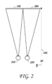
図2は、ユーザのための3次元画像をシミュレートするための従来のディスプレイシステムを図示する。ユーザの眼は、離間されており、空間内の実オブジェクトを見ているとき、各眼は、オブジェクトの若干異なるビューを有し、オブジェクトの画像を各眼の網膜上の異なる場所に形成し得ることを理解されたい。これは、両眼視差と称され得、ヒト視覚系によって、深度の知覚を提供するために利用され得る。従来のディスプレイシステムは、仮想オブジェクトが所望の深度における実オブジェクトであるように各眼によって見えるであろう仮想オブジェクトのビューに対応する、眼210、220毎に1つの同一仮想オブジェクトの若干異なるビューを伴う2つの明確に異なる画像190、200を提示することによって、両眼視差をシミュレートする。これらの画像は、ユーザの視覚系が深度の知覚を導出するために解釈し得る、両眼キューを提供する。
FIG. 2 illustrates a conventional display system for simulating a 3D image for a user. When the user's eyes are spaced apart and looking at a real object in space, each eye may have a slightly different view of the object and form an image of the object at a different location on each eye's retina. Please understand. This may be referred to as binocular disparity and may be exploited by the human visual system to provide depth perception. Conventional display systems present slightly different views of the same virtual object, one for each
図2を継続して参照すると、画像190、200は、z-軸上で距離230だけ眼210、220から離間される。z-軸は、その眼が視認者の直前の光学無限遠におけるオブジェクトを固視している状態の視認者の光学軸と平行である。画像190、200は、平坦であって、眼210、220から固定距離にある。それぞれ、眼210、220に提示される画像内の仮想オブジェクトの若干異なるビューに基づいて、眼は、必然的に、オブジェクトの画像が眼のそれぞれの網膜上の対応する点に来て、単一両眼視を維持するように回転し得る。本回転は、眼210、220のそれぞれの視線を仮想オブジェクトが存在するように知覚される空間内の点上に収束させ得る。結果として、3次元画像の提供は、従来、ユーザの眼210、220の輻輳・開散運動を操作し得、ヒト視覚系が深度の知覚を提供するように解釈する、両眼キューを提供することを伴う。
With continued reference to FIG. 2, the
しかしながら、深度の現実的かつ快適な知覚の生成は、困難である。眼からの異なる距離におけるオブジェクトからの光が、異なる発散量を伴う波面を有することを理解されたい。図3A-3Cは、距離と光線の発散との間の関係を図示する。オブジェクトと眼210との間の距離は、減少距離R1、R2、およびR3の順序で表される。図3A-3Cに示されるように、光線は、オブジェクトまでの距離が減少するにつれてより発散する。逆に言えば、距離が、増加するにつれて、光線は、よりコリメートされる。換言すると、点(オブジェクトまたはオブジェクトの一部)によって生成されるライトフィールドは、点がユーザの眼から離れている距離の関数である、球状波面曲率を有すると言え得る。曲率は、オブジェクトと眼210の間との距離の減少とともに増加する。単眼210のみが、例証を明確にするために、図3A-3Cおよび本明細書の他の図に図示されるが、眼210に関する議論は、視認者の両眼210および220に適用され得る。
However, producing a realistic and comfortable perception of depth is difficult. It should be appreciated that light from objects at different distances from the eye will have wavefronts with different amounts of divergence. 3A-3C illustrate the relationship between distance and ray divergence. The distance between the object and the
図3A-3Cを継続して参照すると、視認者の眼が固視しているオブジェクトからの光が、異なる波面発散度を有し得る。異なる波面発散量に起因して、光は、眼の水晶体によって異なるように集束され得、これは、ひいては、水晶体に、異なる形状をとり、合焦画像を眼の網膜上に形成することを要求し得る。合焦画像が、網膜上に形成されない場合、結果として生じる網膜ぼけは、合焦画像が網膜上に形成されるまで、眼の水晶体の形状に変化を生じさせる、遠近調節のためのキューとして作用する。例えば、遠近調節のためのキューは、眼の水晶体を囲繞する毛様筋の弛緩または収縮を誘起し、それによって、水晶体を保持する提靭帯に印加される力を変調させ、したがって、固視されているオブジェクトの網膜ぼけが排除される、または最小限にされるまで、眼の水晶体の形状を変化させ、それによって、固視されているオブジェクトの合焦画像を眼の網膜(例えば、中心窩)上に形成し得る。眼の水晶体が形状を変化させるプロセスは、遠近調節と称され得、固視されているオブジェクトの合焦画像を眼の網膜(例えば、中心窩)上に形成するために要求される眼の水晶体の形状は、遠近調節状態と称され得る。 With continued reference to FIGS. 3A-3C, light from an object to which the viewer's eye is fixating may have different wavefront divergence. Due to different amounts of wavefront divergence, light may be focused differently by the lens of the eye, which in turn requires the lens to take on different shapes and form a focused image on the retina of the eye. can. If a focused image is not formed on the retina, the resulting retinal blur acts as a cue for accommodation, causing a change in the shape of the eye's lens until a focused image is formed on the retina. do. For example, cues for accommodation induce relaxation or contraction of the ciliary muscle that surrounds the lens of the eye, thereby modulating the force applied to the suspensory ligaments that hold the lens in place, thus causing fixation. The shape of the lens of the eye is changed until the retinal blur of the object being fixated is eliminated or minimized, thereby shifting the focused image of the object being fixated to the retina of the eye (e.g., the fovea). ). The process by which the eye's lens changes shape may be referred to as accommodation, and is required to form a focused image of the object being fixated on the eye's retina (e.g., the fovea). The shape of may be referred to as the accommodation state.
ここで図4Aを参照すると、ヒト視覚系の遠近調節-輻輳・開散運動応答の表現が、図示される。オブジェクトを固視するための眼の移動は、眼にオブジェクトからの光を受光させ、光は、画像を眼の網膜のそれぞれの上に形成する。網膜上に形成される画像内の網膜ぼけの存在は、遠近調節のためのキューを提供し得、網膜上の画像の相対的場所は、輻輳・開散運動のキューを提供し得る。遠近調節のためのキューは、遠近調節を生じさせ、眼の水晶体に、オブジェクトの合焦画像を眼の網膜(例えば、中心窩)上に形成する特定の遠近調節状態をとらせる。一方で、輻輳・開散運動のためのキューは、各眼の各網膜上に形成される画像が、単一両眼視を維持する対応する網膜点にあるように、輻輳・開散運動移動(眼の回転)を生じさせる。これらの位置では、眼は、特定の輻輳・開散運動状態をとっていると言え得る。図4Aを継続して参照すると、遠近調節は、眼が特定の遠近調節状態を達成するプロセスであると理解され得、輻輳・開散運動は、眼が特定の輻輳・開散運動状態を達成するプロセスであると理解され得る。図4Aに示されるように、眼の遠近調節および輻輳・開散運動状態は、ユーザが別のオブジェクトを固視する場合、変化し得る。例えば、遠近調節された状態は、ユーザがz-軸上の異なる深度における新しいオブジェクトを固視する場合、変化し得る。 Referring now to FIG. 4A, a representation of the accommodation-convergence-divergence motor response of the human visual system is illustrated. Movement of the eye to fixate on the object causes the eye to receive light from the object, which light forms an image on each of the retinas of the eye. The presence of retinal blur in the image formed on the retina can provide cues for accommodation, and the relative location of the image on the retina can provide cues for convergence-divergence movement. A cue for accommodation causes accommodation, causing the eye's lens to assume a particular accommodation state that forms a focused image of the object on the eye's retina (eg, the fovea). On the other hand, the cues for convergence-divergence movement are such that the image formed on each retina of each eye is at the corresponding retinal point that maintains single-binocular vision. (eye rotation). At these positions, the eye can be said to be in a particular state of convergence-divergence movement. With continued reference to FIG. 4A, accommodation can be understood as the process by which the eye achieves a particular state of accommodation, and convergence-divergence movement is the process by which the eye achieves a particular state of convergence-divergence movement. can be understood to be the process of As shown in FIG. 4A, the accommodation and convergence-divergence motion states of the eye may change when the user fixes his gaze on another object. For example, the accommodated state may change if the user fixes to a new object at different depths on the z-axis.
理論によって限定されるわけではないが、オブジェクトの視認者は、輻輳・開散運動と遠近調節の組み合わせに起因して、オブジェクトを「3次元」として知覚し得ると考えられる。上記のように、相互に対する2つの眼の輻輳・開散運動移動(例えば、瞳孔が相互に向かって、またはそこから離れるように移動し、眼の視線を収束させ、オブジェクトを固視するような眼の回転)は、眼の水晶体の遠近調節と密接に関連付けられる。通常条件下、眼の水晶体の形状を変化させ、焦点を1つのオブジェクトから異なる距離における別のオブジェクトに変化させることは、自動的に、「遠近調節-輻輳・開散運動反射」として知られる関係下、輻輳・開散運動の合致する変化を自動的に同一距離に生じさせるであろう。同様に、輻輳・開散運動における変化は、通常条件下で、水晶体形状における合致する変化を誘起するであろう。 Without being limited by theory, it is believed that a viewer of an object may perceive the object as "three-dimensional" due to a combination of convergence-divergence motion and accommodation. As described above, the convergence-divergence movement of the two eyes relative to each other (e.g., the pupils moving toward or away from each other, converging the eye's line of sight, and fixating on an object). eye rotation) is closely related to accommodation of the eye's lens. Under normal conditions, changing the shape of the eye's lens and changing focus from one object to another at different distances automatically creates a relationship known as the accommodation-convergence-divergence motor reflex. Underneath, it will automatically produce a matching change of convergence-divergence movement at the same distance. Similarly, changes in convergence-divergence motion will induce congruent changes in lens shape under normal conditions.
ここで図4Bを参照すると、眼の異なる遠近調節および輻輳・開散運動状態の実施例が、図示される。一対の眼222aが、光学無限遠におけるオブジェクトを固視する一方、一対の眼222bは、光学無限遠未満におけるオブジェクト221を固視する。着目すべきこととして、各対の眼の輻輳・開散運動状態は、異なり、一対の眼222aが、まっすぐ指向される一方、一対の眼222は、オブジェクト221上に収束する。各対の眼222aおよび222bを形成する眼の遠近調節状態もまた、水晶体210a、220aの異なる形状によって表されるように異なる。 Referring now to FIG. 4B, examples of different accommodation and convergence-divergence motion states of the eye are illustrated. A pair of eyes 222a fixates on an object at optical infinity, while a pair of eyes 222b fixes on an object 221 below optical infinity. It should be noted that the convergence-divergence motion state of each pair of eyes is different, the pair of eyes 222 a is directed straight while the pair of eyes 222 converges on the object 221 . The accommodation states of the eyes forming each pair of eyes 222a and 222b are also different as represented by the different shapes of the lenses 210a, 220a.
望ましくないことに、従来の「3-D」ディスプレイシステムの多くのユーザは、これらのディスプレイにおける遠近調節と輻輳・開散運動状態との間の不一致に起因して、そのような従来のシステムを不快であると見出す、または奥行感を全く知覚しない場合がある。上記のように、多くの立体視または「3-D」ディスプレイシステムは、若干異なる画像を各眼に提供することによって、場面を表示する。そのようなシステムは、それらが、とりわけ、単に、場面の異なる提示を提供し、眼の輻輳・開散運動状態に変化を生じさせるが、それらの眼の遠近調節状態における対応する変化を伴わないため、多くの視認者にとって不快である。むしろ、画像は、眼が全ての画像情報を単一遠近調節状態において視認するように、ディスプレイによって眼から固定距離に示される。そのような配列は、遠近調節状態における合致する変化を伴わずに輻輳・開散運動状態に変化を生じさせることによって、「遠近調節-輻輳・開散運動反射」に逆らう。本不一致は、視認者の不快感を生じさせると考えられる。遠近調節と輻輳・開散運動との間のより良好な合致を提供する、ディスプレイシステムは、3次元画像のより現実的かつ快適なシミュレーションを形成し得る。 Undesirably, many users of conventional "3-D" display systems prefer such conventional systems due to the mismatch between accommodation and convergence-divergence motion states in these displays. You may find it uncomfortable or not perceive depth at all. As noted above, many stereoscopic or "3-D" display systems display a scene by presenting a slightly different image to each eye. Such systems, among other things, simply provide different presentations of scenes and produce changes in the convergence-divergence movement state of the eyes, but without a corresponding change in their accommodation state. Therefore, it is uncomfortable for many viewers. Rather, the image is presented by the display at a fixed distance from the eye such that the eye sees all image information in a single accommodation state. Such an arrangement counteracts the "accommodation-convergence-divergence movement reflex" by producing changes in the convergence-divergence movement state without a congruent change in accommodation state. This discrepancy is believed to cause viewer discomfort. A display system that provides a better match between accommodation and convergence-divergence movements can produce a more realistic and comfortable simulation of three-dimensional images.
理論によって限定されるわけではないが、ヒトの眼は、典型的には、有限数の深度平面を解釈し、深度知覚を提供し得ると考えられる。その結果、知覚された深度の高度に真実味のあるシミュレーションが、眼にこれらの限定数の深度平面のそれぞれに対応する画像の異なる提示を提供することによって達成され得る。いくつかの実施形態では、異なる提示は、輻輳・開散運動のためのキューおよび遠近調節のための合致するキューの両方を提供し、それによって、生理学的に正しい遠近調節-輻輳・開散運動合致を提供し得る。 Without being limited by theory, it is believed that the human eye can typically interpret a finite number of depth planes to provide depth perception. As a result, a highly believable simulation of perceived depth can be achieved by presenting the eye with different presentations of images corresponding to each of these limited number of depth planes. In some embodiments, the different presentations provide both cues for convergence-divergence movements and matching cues for accommodation, thereby providing physiologically correct accommodation-convergence-divergence movements. can provide a match.
図4Bを継続して参照すると、眼210、220からの空間内の異なる距離に対応する、2つの深度平面240が、図示される。所与の深度平面240に関して、輻輳・開散運動キューが、眼210、220毎に適切に異なる視点の画像を表示することによって提供されてもよい。加えて、所与の深度平面240に関して、各眼210、220に提供される画像を形成する光は、その深度平面240の距離におけるある点によって生成されたライトフィールドに対応する波面発散を有してもよい。
With continued reference to FIG. 4B, two
図示される実施形態では、点221を含有する、深度平面240のz-軸に沿った距離は、1mである。本明細書で使用されるように、z-軸に沿った距離または深度は、ユーザの眼の射出瞳に位置するゼロ点を用いて測定されてもよい。したがって、1mの深度に位置する深度平面240は、眼が光学無限遠に向かって指向された状態でそれらの眼の光学軸上のユーザの眼の射出瞳から1m離れた距離に対応する。近似値として、z-軸に沿った深度または距離は、ユーザの眼の正面のディスプレイから(例えば、導波管の表面から)測定され、デバイスとユーザの眼の射出瞳との間の距離に関する値が加えられてもよい。その値は、瞳距離と呼ばれ得、ユーザの眼の射出瞳と眼の正面のユーザによって装着されるディスプレイとの間の距離に対応する。実践では、瞳距離に関する値は、概して、全ての視認者に使用される、正規化された値であってもよい。例えば、瞳距離は、20mmであると仮定され得、1mの深度における深度平面は、ディスプレイの正面の980mmの距離にあり得る。
In the illustrated embodiment, the distance along the z-axis of
ここで図4Cおよび4Dを参照すると、合致遠近調節-輻輳・開散運動距離および不一致遠近調節-輻輳・開散運動距離の実施例が、それぞれ、図示される。図4Cに図示されるように、ディスプレイシステムは、仮想オブジェクトの画像を各眼210、220に提供してもよい。画像は、眼210、220に、眼が深度平面240上の点15上に収束する、輻輳・開散運動状態をとらせ得る。加えて、画像は、その深度平面240における実オブジェクトに対応する波面曲率を有する、光によって形成され得る。結果として、眼210、220は、画像がそれらの眼の網膜上で合焦する、遠近調節状態をとる。したがって、ユーザは、仮想オブジェクトを深度平面240上の点15にあるものとして知覚し得る。
4C and 4D, examples of congruent accommodation-convergence-divergence movement distance and discordance accommodation-convergence-divergence movement distance, respectively, are illustrated. The display system may provide an image of the virtual object to each
眼210、220の遠近調節および輻輳・開散運動状態はそれぞれ、z-軸上の特定の距離と関連付けられることを理解されたい。例えば、眼210、220からの特定の距離におけるオブジェクトは、それらの眼に、オブジェクトの距離に基づいて、特定の遠近調節状態をとらせる。特定の遠近調節状態と関連付けられる距離は、遠近調節距離Adと称され得る。同様に、特定の輻輳・開散運動状態または相互に対する位置における眼と関連付けられた特定の輻輳・開散運動距離Vdが、存在する。遠近調節距離および輻輳・開散運動距離が合致する場合、遠近調節と輻輳・開散運動との間の関係は、生理学的に正しいと言える。これは、視認者にとって最も快適なシナリオであると見なされる。
It should be appreciated that the accommodation and convergence-divergence motion states of the
しかしながら、立体視ディスプレイでは、遠近調節距離および輻輳・開散運動距離は、常に合致するわけではない場合がある。例えば、図4Dに図示されるように、眼210、220に表示される画像は、深度平面240に対応する波面発散を伴って表示され得、眼210、220は、その深度平面上の点15a、15bが合焦する、特定の遠近調節状態をとり得る。しかしながら、眼210、220に表示される画像は、眼210、220を深度平面240上に位置しない点15上に収束させる、輻輳・開散運動のためのキューを提供し得る。結果として、遠近調節距離は、いくつかの実施形態では、眼210、220の射出瞳から深度平面240への距離に対応する一方、輻輳・開散運動距離は、眼210、220の射出瞳から点15までのより大きい距離に対応する。遠近調節距離は、輻輳・開散運動距離と異なる。その結果、遠近調節-輻輳・開散運動の不一致が存在する。そのような不一致は、望ましくないと見なされ、不快感をユーザに生じさせ得る。不一致は、距離(例えば、Vd-Ad)に対応し、ジオプタを使用して特性評価され得ることを理解されたい。
However, in stereoscopic displays, the accommodation distance and the convergence-divergence motion distance may not always match. For example, as illustrated in FIG. 4D, an image displayed on the
いくつかの実施形態では、眼210、220の射出瞳以外の参照点も、同一参照点が遠近調節距離および輻輳・開散運動距離のために利用される限り、遠近調節-輻輳・開散運動の不一致を決定するための距離を決定するために利用され得ることを理解されたい。例えば、距離は、角膜から深度平面まで、網膜から深度平面まで、接眼レンズ(例えば、ディスプレイデバイスの導波管)から深度平面まで、眼の回転中心から等、測定され得る。
In some embodiments, reference points other than the exit pupil of the
理論によって限定されるわけではないが、ユーザは、不一致自体が有意な不快感を生じさせることなく、依然として、最大約0.25ジオプタ、最大約0.33ジオプタ、および最大約0.5ジオプタの遠近調節-輻輳・開散運動の不一致を生理学的に正しいと知覚し得ると考えられる。いくつかの実施形態では、本明細書に開示されるディスプレイシステム(例えば、ディスプレイシステム250、図6)は、約0.5ジオプタまたはそれ未満の遠近調節-輻輳・開散運動の不一致を有する、画像を視認者に提示する。いくつかの他の実施形態では、ディスプレイシステムによって提供される画像の遠近調節-輻輳・開散運動の不一致は、約0.33ジオプタまたはそれ未満である。さらに他の実施形態では、ディスプレイシステムによって提供される画像の遠近調節-輻輳・開散運動の不一致は、約0.1ジオプタまたはそれ未満を含む、約0.25ジオプタまたはそれ未満である。 Without wishing to be limited by theory, users can still achieve up to about 0.25 diopters, up to about 0.33 diopters, and up to about 0.5 diopters without the discrepancy itself causing significant discomfort. It is thought that accommodative-convergence-divergence discrepancies can be perceived as physiologically correct. In some embodiments, a display system disclosed herein (eg, display system 250, FIG. 6) has an accommodation-convergence-divergence mismatch of about 0.5 diopters or less, Present the image to the viewer. In some other embodiments, the accommodation-convergence-divergence motion mismatch of images provided by the display system is about 0.33 diopters or less. In still other embodiments, the accommodation-convergence-divergence motion mismatch of images provided by the display system is about 0.25 diopters or less, including about 0.1 diopters or less.
図5は、波面発散を修正することによって、3次元画像をシミュレートするためのアプローチの側面を図示する。ディスプレイシステムは、画像情報でエンコードされる光770を受光し、その光をユーザの眼210に出力するように構成される、導波管270を含む。導波管270は、所望の深度平面240上のある点によって生成されるライトフィールドの波面発散に対応する、定義された波面発散量を伴って光650を出力してもよい。いくつかの実施形態では、同一量の波面発散が、その深度平面上に提示される全てのオブジェクトのために提供される。加えて、ユーザの他方の眼は、類似導波管からの画像情報を提供され得ることが図示されるであろう。
FIG. 5 illustrates aspects of an approach for simulating three-dimensional images by correcting for wavefront divergence. The display system includes a
いくつかの実施形態では、単一の導波管が、単一または限定数の深度平面に対応する設定された波面発散量を伴う光を出力するように構成されてもよい、および/または導波管は、限定された範囲の波長の光を出力するように構成されてもよい。その結果、いくつかの実施形態では、複数またはスタックの導波管が、異なる深度平面のための異なる波面発散量を提供する、および/または異なる範囲の波長の光を出力するために利用されてもよい。本明細書で使用されるように、深度平面は、平坦または湾曲表面の輪郭に追従し得ることを理解されたい。いくつかの実施形態では、有利なこととして、簡略化するために、深度平面は、平坦表面の輪郭に追従し得る。 In some embodiments, a single waveguide may be configured and/or guided to output light with a set amount of wavefront divergence corresponding to a single or limited number of depth planes. A wave tube may be configured to output a limited range of wavelengths of light. As a result, in some embodiments, multiple or stacks of waveguides are utilized to provide different amounts of wavefront divergence for different depth planes and/or output different ranges of wavelengths of light. good too. As used herein, it should be appreciated that a depth plane can follow the contour of a flat or curved surface. In some embodiments, the depth plane may advantageously follow the contour of the planar surface for simplicity.
図6は、画像情報をユーザに出力するための導波管スタックの実施例を図示する。ディスプレイシステム250は、複数の導波管270、280、290、300、310を使用して3次元知覚を眼/脳に提供するために利用され得る、導波管のスタックまたはスタックされた導波管アセンブリ260を含む。ディスプレイシステム250は、いくつかの実施形態では、ライトフィールドディスプレイと見なされ得ることを理解されたい。加えて、導波管アセンブリ260はまた、接眼レンズとも称され得る。
FIG. 6 illustrates an example waveguide stack for outputting image information to a user. Display system 250 may be utilized to provide three-dimensional perception to the eye/brain using
いくつかの実施形態では、ディスプレイシステム250は、輻輳・開散運動するための実質的に連続的なキューおよび遠近調節のための複数の離散キューを提供するように構成されてもよい。輻輳・開散運動のためのキューは、異なる画像をユーザの眼のそれぞれに表示することによって提供されてもよく、遠近調節のためのキューは、選択可能な離散量の波面発散を伴う画像を形成する光を出力することによって提供されてもよい。換言すると、ディスプレイシステム250は、可変レベルの波面発散を伴う光を出力するように構成されてもよい。いくつかの実施形態では、波面発散の各離散レベルが、特定の深度平面に対応し、導波管270、280、290、300、310のうちの特定のものによって提供されてもよい。
In some embodiments, display system 250 may be configured to provide substantially continuous cues for convergence-divergence movements and multiple discrete cues for accommodation. Cues for convergence-divergence movements may be provided by displaying a different image to each of the user's eyes, and cues for accommodation may present images with selectable discrete amounts of wavefront divergence. It may be provided by outputting light forming. In other words, display system 250 may be configured to output light with varying levels of wavefront divergence. In some embodiments, each discrete level of wavefront divergence corresponds to a particular depth plane and may be provided by a particular one of
図6を継続して参照すると、導波管アセンブリ260はまた、複数の特徴320、330、340、350を導波管の間に含んでもよい。いくつかの実施形態では、特徴320、330、340、350は、1つ以上のレンズであってもよい。導波管270、280、290、300、310、および/または複数のレンズ320、330、340、350は、種々のレベルの波面曲率または光線発散を用いて画像情報を眼に送信するように構成されてもよい。各導波管レベルは、特定の深度平面と関連付けられてもよく、その深度平面に対応する画像情報を出力するように構成されてもよい。画像投入デバイス360、370、380、390、400は、導波管のための光源として機能してもよく、それぞれ、本明細書に説明されるように、眼210に向かって出力するために、各個別の導波管を横断して入射光を分散させるように構成され得る、導波管270、280、290、300、310の中に画像情報を投入するために利用されてもよい。光は、画像投入デバイス360、370、380、390、400の出力表面410、420、430、440、450から出射し、導波管270、280、290、300、310の対応する入力表面460、470、480、490、500の中に投入される。いくつかの実施形態では、入力表面460、470、480、490、500はそれぞれ、対応する導波管の縁であってもよい、または対応する導波管の主要表面の一部(すなわち、世界510または視認者の眼210に直接面する導波管表面のうちの1つ)であってもよい。導波管の主要表面は、その間に導波管の厚さが延在する、導波管の表面に対応することを理解されたい。いくつかの実施形態では、光の単一ビーム(例えば、コリメートされたビーム)が、各導波管の中に投入され、特定の導波管と関連付けられた深度平面に対応する特定の角度(および発散量)において眼210に向かって指向される、クローン化されるコリメートビームの場全体を出力してもよい。いくつかの実施形態では、画像投入デバイス360、370、380、390、400のうちの単一のものが、複数(例えば、3つ)の導波管270、280、290、300、310と関連付けられ、その中に光を投入してもよい。
With continued reference to FIG. 6, waveguide assembly 260 may also include a plurality of features 320, 330, 340, 350 between the waveguides. In some embodiments, features 320, 330, 340, 350 may be one or more lenses.
いくつかの実施形態では、画像投入デバイス360、370、380、390、400は、それぞれ、対応する導波管270、280、290、300、310の中への投入のための画像情報をそれぞれ生成する、離散ディスプレイである。いくつかの他の実施形態では、画像投入デバイス360、370、380、390、400は、例えば、1つ以上の光学導管(光ファイバケーブル等)を介して、画像情報を画像投入デバイス360、370、380、390、400のそれぞれに送り得る、単一の多重化されたディスプレイの出力端である。画像投入デバイス360、370、380、390、400によって提供される画像情報は、異なる波長または色(例えば、本明細書に議論されるように、異なる原色)の光を含み得ることを理解されたい。
In some embodiments, image injection devices 360, 370, 380, 390, 400 each generate image information for injection into
いくつかの実施形態では、導波管270、280、290、300、310の中に投入される光は、発光ダイオード(LED)等の光エミッタを含み得る、光モジュール530を備える、光プロジェクタシステム520によって提供される。光モジュール530からの光は、ビームスプリッタ550を介して、光変調器540、例えば、空間光変調器に指向され、それによって修正されてもよい。光変調器540は、導波管270、280、290、300、310の中に投入される光の知覚される強度を変化させ、光を画像情報でエンコードするように構成されてもよい。空間光変調器の実施例は、シリコン上液晶(LCOS)ディスプレイを含む、液晶ディスプレイ(LCD)を含む。画像投入デバイス360、370、380、390、400は、図式的に図示され、いくつかの実施形態では、これらの画像投入デバイスは、光を導波管270、280、290、300、310の関連付けられるものの中に出力するように構成される、共通投影システム内の異なる光経路および場所を表し得ることを理解されたい。いくつかの実施形態では、導波管アセンブリ260の導波管は、導波管の中に投入される光をユーザの眼に中継しながら、理想的レンズとして機能し得る。本概念では、オブジェクトは、空間光変調器540であってもよく、画像は、深度平面上の画像であってもよい。
In some embodiments, the light injected into
いくつかの実施形態では、ディスプレイシステム250は、光を種々のパターン(例えば、ラスタ走査、螺旋走査、リサジューパターン等)で1つ以上の導波管270、280、290、300、310の中に、最終的には、視認者の眼210に投影するように構成される、1つ以上の走査ファイバを備える、走査ファイバディスプレイであってもよい。いくつかの実施形態では、図示される画像投入デバイス360、370、380、390、400は、光を1つまたは複数の導波管270、280、290、300、310の中に投入するように構成される、単一走査ファイバまたは走査ファイバの束を図式的に表し得る。いくつかの他の実施形態では、図示される画像投入デバイス360、370、380、390、400は、それぞれ、光を導波管270、280、290、300、310のうちの関連付けられるものの中に投入するように構成される、複数の走査ファイバまたは走査ファイバの複数の束を図式的に表し得る。1つ以上の光ファイバは、光を光モジュール530から1つ以上の導波管270、280、290、300、310に透過させるように構成され得ることを理解されたい。1つ以上の介在光学構造が、走査ファイバまたは複数のファイバと、1つ以上の導波管270、280、290、300、310との間に提供され、例えば、走査ファイバから出射する光を1つ以上の導波管270、280、290、300、310の中に再指向し得ることを理解されたい。
In some embodiments, display system 250 directs light into one or
コントローラ560は、画像投入デバイス360、370、380、390、400、光源530、および光モジュール540の動作を含む、スタックされた導波管アセンブリ260のうちの1つ以上のものの動作を制御する。いくつかの実施形態では、コントローラ560は、ローカルデータ処理モジュール140の一部である。コントローラ560は、例えば、本明細書に開示される種々のスキームのいずれかに従って、導波管270、280、290、300、310への画像情報のタイミングおよび提供を調整する、プログラミング(例えば、非一過性媒体内の命令)を含む。いくつかの実施形態では、コントローラは、単一の一体型デバイスまたは有線または無線通信チャネルによって接続される分散型システムであってもよい。コントローラ560は、いくつかの実施形態では、処理モジュール140または150(図9D)の一部であってもよい。 Controller 560 controls operation of one or more of stacked waveguide assemblies 260 , including operation of image input devices 360 , 370 , 380 , 390 , 400 , light source 530 , and light module 540 . In some embodiments, controller 560 is part of local data processing module 140 . Controller 560 may be programmed (e.g., non instructions in transient media). In some embodiments, the controller may be a single integrated device or a distributed system connected by wired or wireless communication channels. Controller 560 may be part of processing module 140 or 150 (FIG. 9D) in some embodiments.
図6を継続して参照すると、導波管270、280、290、300、310は、全内部反射(TIR)によって各個別の導波管内で光を伝搬するように構成されてもよい。導波管270、280、290、300、310はそれぞれ、主要上部表面および主要底部表面およびそれらの主要上部表面と主要底部表面との間に延在する縁を伴う、平面である、または別の形状(例えば、湾曲)を有してもよい。図示される構成では、導波管270、280、290、300、310はそれぞれ、各個別の導波管内で伝搬する光を導波管から外に再指向させ、画像情報を眼210に出力することによって、光を導波管から抽出するように構成される、外部結合光学要素570、580、590、600、610を含んでもよい。抽出された光はまた、外部結合光と称され得、外部結合光学要素はまた、光抽出光学要素と称され得る。抽出された光のビームは、導波管によって、導波管内で伝搬する光が光抽出光学要素に衝打する場所において出力され得る。外部結合光学要素570、580、590、600、610は、例えば、本明細書にさらに議論されるような回折光学特徴を含む、格子であってもよい。説明を容易にし、図面を明確にするために、導波管270、280、290、300、310の底部主要表面に配置されて図示されるが、いくつかの実施形態では、外部結合光学要素570、580、590、600、610は、本明細書にさらに議論されるように、上部および/または底部主要表面に配置されてもよい、および/または導波管270、280、290、300、310の容積内に直接配置されてもよい。いくつかの実施形態では、外部結合光学要素570、580、590、600、610は、透明基板に取り付けられ、導波管270、280、290、300、310を形成する、材料の層内に形成されてもよい。いくつかの他の実施形態では、導波管270、280、290、300、310は、モノリシック材料部品であってもよく、外部結合光学要素570、580、590、600、610は、その材料部品の表面上および/または内部に形成されてもよい。
With continued reference to FIG. 6,
図6を継続して参照すると、本明細書に議論されるように、各導波管270、280、290、300、310は、光を出力し、特定の深度平面に対応する画像を形成するように構成される。例えば、眼の最近傍の導波管270は、眼210にコリメートされた光(そのような導波管270の中に投入された)を送達するように構成されてもよい。コリメートされた光は、光学無限遠焦点面を表し得る。次の上方の導波管280は、眼210に到達し得る前に、第1のレンズ350(例えば、負のレンズ)を通して通過する、コリメートされた光を送出するように構成されてもよい。そのような第1のレンズ350は、眼/脳が、その次の上方の導波管280から生じる光を光学無限遠から眼210に向かって内向きにより近い第1の焦点面から生じるものとして解釈するように、若干の凸面波面曲率を生成するように構成されてもよい。同様に、第3の上方の導波管290は、眼210に到達する前に、その出力光を第1のレンズ350および第2のレンズ340の両方を通して通過させる。第1のレンズ350および第2のレンズ340の組み合わせられた屈折力は、眼/脳が、第3の上方の導波管290から生じる光が次の上方の導波管280からの光であった光学無限遠から人物に向かって内向きにさらに近い第2の焦点面から生じるものとして解釈するように、別の漸増量の波面曲率を生成するように構成されてもよい。
With continued reference to FIG. 6, each
他の導波管層300、310およびレンズ330、320も同様に構成され、スタック内の最高導波管310が、人物に最も近い焦点面を表す集約焦点力のために、その出力をそれと眼との間のレンズの全てを通して送出する。スタックされた導波管アセンブリ260の他側の世界510から生じる光を視認/解釈するとき、レンズ320、330、340、350のスタックを補償するために、補償レンズ層620が、スタックの上部に配置され、下方のレンズスタック320、330、340、350の集約力を補償してもよい。そのような構成は、利用可能な導波管/レンズ対と同じ数の知覚される焦点面を提供する。導波管の外部結合光学要素およびレンズの集束側面は両方とも、静的であってもよい(すなわち、動的ではないまたは電気活性ではない)。いくつかの代替実施形態では、いずれか一方または両方とも、電気活性特徴を使用して動的であってもよい。 The other waveguide layers 300, 310 and lenses 330, 320 are similarly configured, with the highest waveguide 310 in the stack directing its output between it and the eye due to the aggregate focal power representing the focal plane closest to the person. through all of the lenses between To compensate the stack of lenses 320, 330, 340, 350 when viewing/interpreting light originating from the world 510 on the other side of the stacked waveguide assembly 260, a compensating lens layer 620 is placed on top of the stack. may be arranged to compensate for the collective power of the lens stacks 320, 330, 340, 350 below. Such a configuration provides as many perceived focal planes as there are waveguide/lens pairs available. Both the out-coupling optical element of the waveguide and the focusing side of the lens may be static (ie, not dynamic or electroactive). In some alternative embodiments, either or both may be dynamic using electro-active features.
いくつかの実施形態では、導波管270、280、290、300、310のうちの2つ以上のものは、同一の関連付けられる深度平面を有してもよい。例えば、複数の導波管270、280、290、300、310が、同一深度平面に設定される画像を出力するように構成されてもよい、または導波管270、280、290、300、310の複数のサブセットが、深度平面毎に1つのセットを用いて、同一の複数の深度平面に設定される画像を出力するように構成されてもよい。これは、それらの深度平面において拡張された視野を提供するようにタイル化された画像を形成するための利点を提供し得る。
In some embodiments, two or more of
図6を継続して参照すると、外部結合光学要素570、580、590、600、610は、導波管と関連付けられた特定の深度平面のために、光をそれらの個別の導波管から外に再指向し、かつ本光を適切な量の発散またはコリメーションを伴って出力するように構成されてもよい。その結果、異なる関連付けられた深度平面を有する導波管が、関連付けられた深度平面に応じて、異なる量の発散を伴う光を出力する、外部結合光学要素570、580、590、600、610の異なる構成を有してもよい。いくつかの実施形態では、光抽出光学要素570、580、590、600、610は、光を具体的角度で出力するように構成され得る、立体または表面特徴であってもよい。例えば、光抽出光学要素570、580、590、600、610は、立体ホログラム、表面ホログラム、および/または回折格子であってもよい。いくつかの実施形態では、特徴320、330、340、350は、レンズではなくてもよい。むしろ、それらは、単に、スペーサ(例えば、クラッディング層および/または空隙を形成するための構造)であってもよい。
With continued reference to FIG. 6, the out-coupling
いくつかの実施形態では、外部結合光学要素570、580、590、600、610は、回折パターンを形成する回折特徴または「回折光学要素」(本明細書では、「DOE」とも称される)である。好ましくは、DOEは、ビームの光の一部のみが、DOEの各交差部で眼210に向かって偏向される一方、残りが、TIRを介して、導波管を通して移動し続けるように、十分に低回折効率を有する。画像情報を搬送する光は、したがって、複数の場所において導波管から出射する、いくつかの関連出射ビームに分割され、その結果、導波管内でバウンスする本特定のコリメートされたビームに関して、眼210に向かって非常に均一なパターンの出射放出となる。
In some embodiments, the out-coupling
いくつかの実施形態では、1つ以上のDOEは、能動的に回折する「オン」状態と有意に回折しない「オフ」状態との間で切替可能であってもよい。例えば、切替可能なDOEは、ポリマー分散液晶の層を備えてもよく、その中で微小液滴は、ホスト媒体内に回折パターンを備え、微小液滴の屈折率は、ホスト材料の屈折率に実質的に合致するように切り替えられてもよい(その場合、パターンは、入射光を著しく回折させない)、または微小液滴は、ホスト媒体のものに合致しない屈折率に切り替えられてもよい(その場合、パターンは、入射光を能動的に回折させる)。 In some embodiments, one or more of the DOEs may be switchable between an actively diffracting "on" state and a non-significantly diffracting "off" state. For example, a switchable DOE may comprise a layer of polymer-dispersed liquid crystal, in which the microdroplets comprise a diffraction pattern in the host medium, and the refractive index of the microdroplets matches the refractive index of the host material. It may be switched to substantially match (where the pattern does not significantly diffract incident light) or the microdroplet may be switched to a refractive index that does not match that of the host medium (which pattern actively diffracts incident light).
いくつかの実施形態では、カメラアセンブリ630(例えば、可視光および赤外線光カメラを含む、デジタルカメラ)が、眼210および/または眼210の周囲の組織の画像を捕捉し、例えば、ユーザ入力を検出する、および/またはユーザの生理学的状態を監視するために提供されてもよい。本明細書で使用されるように、カメラは、任意の画像捕捉デバイスであってもよい。いくつかの実施形態では、カメラアセンブリ630は、画像捕捉デバイスと、光(例えば、赤外線光)を眼に投影し、次いで、その光が眼によって反射され、画像捕捉デバイスによって検出され得る、光源とを含んでもよい。いくつかの実施形態では、カメラアセンブリ630は、フレーム80(図9D)に取り付けられてもよく、カメラアセンブリ630からの画像情報を処理し得る、処理モジュール140および/または150と電気通信してもよい。いくつかの実施形態では、1つのカメラアセンブリ630が、眼毎に利用され、各眼を別個に監視してもよい。
In some embodiments, camera assembly 630 (e.g., a digital camera, including visible light and infrared light cameras) captures images of
ここで図7を参照すると、導波管によって出力される出射ビームの実施例が、示される。1つの導波管が図示されるが、導波管アセンブリ260(図6)内の他の導波管も同様に機能し得、導波管アセンブリ260は、複数の導波管を含むことを理解されたい。光640が、導波管270の入力表面460において導波管270の中に投入され、TIRによって導波管270内を伝搬する。光640がDOE570上に衝突する点では、光の一部は、導波管から出射ビーム650として出射する。出射ビーム650は、略平行として図示されるが、本明細書に議論されるように、それらはまた、導波管270と関連付けられた深度平面に応じて、ある角度において眼210に伝搬する(例えば、発散出射ビームを形成する)ように再指向されてもよい。略平行出射ビームは、眼210からの遠距離(例えば、光学無限遠)における深度平面上に設定されるように現れる画像を形成するように光を外部結合する、外部結合光学要素を伴う導波管を示し得ることを理解されたい。他の導波管または他の外部結合光学要素のセットは、より発散する、出射ビームパターンを出力してもよく、これは、眼210がより近い距離に遠近調節し、網膜に合焦させることを要求し、光学無限遠より眼210に近い距離からの光として脳によって解釈されるであろう。
Referring now to FIG. 7, an example of an output beam output by a waveguide is shown. Although one waveguide is shown, other waveguides in waveguide assembly 260 (FIG. 6) may function similarly, and waveguide assembly 260 includes multiple waveguides. be understood.
いくつかの実施形態では、フルカラー画像が、原色、例えば、3つ以上の原色のそれぞれにおいて画像をオーバーレイすることによって、各深度平面において形成されてもよい。図8は、各深度平面が、複数の異なる原色を使用して形成される画像を含む、スタックされた導波管アセンブリの実施例を図示する。図示される実施形態は、深度平面240a-240fを示すが、より多いまたはより少ない深度もまた、検討される。各深度平面は、第1の色Gの第1の画像、第2の色Rの第2の画像、および第3の色Bの第3の画像を含む、それと関連付けられる3つ以上の原色画像を有してもよい。異なる深度平面が、文字G、R、およびBに続くジオプタ(dpt)に関する異なる数字によって図に示される。単なる実施例として、これらの文字のそれぞれに続く数字は、ジオプタ(1/m)、すなわち、視認者からの深度平面の逆距離を示し、図中の各ボックスは、個々の原色画像を表す。いくつかの実施形態では、異なる波長の光の眼の集束における差異を考慮するために、異なる原色に関する深度平面の正確な設置が、変動し得る。例えば、所与の深度平面に関する異なる原色画像が、ユーザからの異なる距離に対応する深度平面上に設置されてもよい。そのような配列は、視力およびユーザ快適性を増加させ得る、および/または色収差を減少させ得る。 In some embodiments, a full-color image may be formed at each depth plane by overlaying images in each of the primary colors, eg, three or more primary colors. FIG. 8 illustrates an example of a stacked waveguide assembly in which each depth plane contains images formed using multiple different primary colors. Although the illustrated embodiment shows depth planes 240a-240f, greater or lesser depths are also contemplated. Each depth plane has three or more primary color images associated with it, including a first image of a first color G, a second image of a second color R, and a third image of a third color B may have Different depth planes are indicated in the figure by different numbers in diopters (dpt) following the letters G, R, and B. FIG. By way of example only, the numbers following each of these letters indicate diopters (1/m), the inverse distance of the depth plane from the viewer, and each box in the figure represents an individual primary color image. In some embodiments, the exact placement of depth planes for different primary colors may vary to account for differences in the eye's focusing of different wavelengths of light. For example, different primary color images for a given depth plane may be placed on depth planes corresponding to different distances from the user. Such an arrangement may increase vision and user comfort, and/or reduce chromatic aberration.
いくつかの実施形態では、各原色の光が、単一の専用導波管によって出力されてもよく、その結果、各深度平面が、それと関連付けられる複数の導波管を有してもよい。そのような実施形態では、文字G、R、またはBを含む、図中の各ボックスが、個々の導波管を表すと理解され得、3つの導波管が、3つの原色画像が深度平面毎に提供される、深度平面毎に提供されてもよい。各深度平面と関連付けられる導波管は、本図面では、説明を容易にするために相互に隣接して示されるが、物理的デバイスでは、導波管は全て、レベル毎に1つの導波管を伴うスタックで配列され得ることを理解されたい。いくつかの他の実施形態では、複数の原色が、例えば、単一の導波管のみが深度平面毎に提供され得るように、同一導波管によって出力されてもよい。 In some embodiments, each primary color of light may be output by a single dedicated waveguide, such that each depth plane may have multiple waveguides associated with it. In such an embodiment, each box in the figure containing the letter G, R, or B may be understood to represent an individual waveguide, three waveguides and three primary color images in the depth plane It may also be provided per depth plane, provided per depth plane. The waveguides associated with each depth plane are shown adjacent to each other in this figure for ease of illustration, but in the physical device the waveguides are all one waveguide per level. can be arranged in a stack with . In some other embodiments, multiple primary colors may be output by the same waveguide, eg, only a single waveguide may be provided per depth plane.
図8を継続して参照すると、いくつかの実施形態では、Gは、緑色であって、Rは、赤色であって、Bは、青色である。いくつかの他の実施形態では、マゼンタ色およびシアン色を含む、光の他の波長と関連付けられる他の色も、赤色、緑色、または青色のうちの1つ以上のものに加えて使用されてもよい、またはそれらに取って代わってもよい。 With continued reference to FIG. 8, in some embodiments, G is green, R is red, and B is blue. In some other embodiments, other colors associated with other wavelengths of light, including magenta and cyan, are also used in addition to one or more of red, green, or blue. may be used or may replace them.
本開示の全体を通した所与の光の色の言及は、視認者によってその所与の色であるものとして知覚される、光の波長の範囲内の1つ以上の波長の光を包含すると理解されるであろうことを理解されたい。例えば、赤色光は、約620~780nmの範囲内の1つ以上の波長の光を含んでもよく、緑色光は、約492~577nmの範囲内の1つ以上の波長の光を含んでもよく、青色光は、約435~493nmの範囲内の1つ以上の波長の光を含んでもよい。 References to a given color of light throughout this disclosure are meant to encompass one or more wavelengths of light within the range of wavelengths of light that are perceived by a viewer to be that given color. It should be understood that it will be understood. For example, red light may include light of one or more wavelengths within the range of about 620-780 nm, green light may include light of one or more wavelengths within the range of about 492-577 nm, Blue light may include light of one or more wavelengths within the range of approximately 435-493 nm.
いくつかの実施形態では、光源530(図6)は、視認者の視覚的知覚範囲外の1つ以上の波長、例えば、赤外線および/または紫外線波長の光を放出するように構成されてもよい。加えて、ディスプレイ250の導波管の内部結合、外部結合、および他の光再指向構造は、例えば、結像および/またはユーザ刺激用途のために、本光をディスプレイからユーザの眼210に向かって指向および放出するように構成されてもよい。
In some embodiments, the light source 530 (FIG. 6) may be configured to emit light at one or more wavelengths outside the visual perception range of the viewer, e.g., infrared and/or ultraviolet wavelengths. . Additionally, waveguide incoupling, outcoupling, and other light redirecting structures of display 250 direct this light from the display toward user's
ここで図9Aを参照すると、いくつかの実施形態では、導波管に衝突する光は、その光を導波管の中に内部結合するために再指向される必要があり得る。内部結合光学要素が、光をその対応する導波管の中に再指向および内部結合するために使用されてもよい。図9Aは、それぞれ、内部結合光学要素を含む、複数またはセット660のスタックされた導波管の実施例の断面側面図を図示する。導波管はそれぞれ、1つ以上の異なる波長または1つ以上の異なる波長範囲の光を出力するように構成されてもよい。スタック660は、スタック260(図6)に対応し得、スタック660の図示される導波管は、画像投入デバイス360、370、380、390、400のうちの1つ以上のものからの光が、光が内部結合のために再指向されることを要求する位置から導波管の中に投入されることを除いて、複数の導波管270、280、290、300、310の一部に対応し得ることを理解されたい。
Referring now to FIG. 9A, in some embodiments, light impinging on the waveguide may need to be redirected to incoupling the light into the waveguide. Incoupling optical elements may be used to redirect and incouple light into its corresponding waveguide. FIG. 9A illustrates a cross-sectional side view of an example of a plurality or set 660 of stacked waveguides, each including an incoupling optical element. Each waveguide may be configured to output light of one or more different wavelengths or one or more different wavelength ranges.
スタックされた導波管の図示されるセット660は、導波管670、680、および690を含む。各導波管は、関連付けられる内部結合光学要素(導波管上の光入力面積とも称され得る)を含み、例えば、内部結合光学要素700は、導波管670の主要表面(例えば、上側主要表面)上に配置され、内部結合光学要素710は、導波管680の主要表面(例えば、上側主要表面)上に配置され、内部結合光学要素720は、導波管690の主要表面(例えば、上側主要表面)上に配置される。いくつかの実施形態では、内部結合光学要素700、710、720のうちの1つ以上のものは、個別の導波管670、680、690の底部主要表面上に配置されてもよい(特に、1つ以上の内部結合光学要素が、反射性偏向光学要素である場合)。図示されるように、内部結合光学要素700、710、720は、特に、それらの内部結合光学要素が、透過性偏向光学要素である場合に、それらの個別の導波管670、680、690の上側主要表面(または次の下側導波管の上部)上に配置されてもよい。いくつかの実施形態では、内部結合光学要素700、710、720は、個別の導波管670、680、690の本体内に配置されてもよい。いくつかの実施形態では、本明細書に議論されるように、内部結合光学要素700、710、720は、他の光の波長を透過させながら、1つ以上の光の波長を選択的に再指向するように、波長選択的である。それらの個別の導波管670、680、690の片側または角に図示されるが、内部結合光学要素700、710、720は、いくつかの実施形態では、それらの個別の導波管670、680、690の他の面積内に配置され得ることを理解されたい。
The illustrated set 660 of stacked waveguides includes
図示されるように、内部結合光学要素700、710、720は、相互から側方にオフセットされてもよい。いくつかの実施形態では、各内部結合光学要素は、光が別の内部結合光学要素を通して通過することなく、その光を受光するようにオフセットされてもよい。例えば、各内部結合光学要素700、710、720は、図6に示されるように、光を異なる画像投入デバイス360、370、380、390、および400から受光するように構成されてもよく、光を内部結合光学要素700、710、720の他のものから実質的に受光しないように、他の内部結合光学要素700、710、720から分離されてもよい(例えば、側方に離間される)。
As shown, the incoupling
各導波管はまた、関連付けられる光分散要素を含み、例えば、光分散要素730は、導波管670の主要表面(例えば、上部主要表面)上に配置され、光分散要素740は、導波管680の主要表面(例えば、上部主要表面)上に配置され、光分散要素750は、導波管690の主要表面(例えば、上部主要表面)上に配置される。いくつかの他の実施形態では、光分散要素730、740、750は、それぞれ、関連付けられる導波管670、680、690の底部主要表面上に配置されてもよい。いくつかの他の実施形態では、光分散要素730、740、750は、それぞれ、関連付けられる導波管670、680、690の上部および底部両方の主要表面上に配置されてもよい、または光分散要素730、740、750は、それぞれ、異なる関連付けられる導波管670、680、690内の上部主要表面および底部主要表面のうちの異なるものの上に配置されてもよい。
Each waveguide also includes an associated light dispersive element, eg, light
導波管670、680、690は、例えば、材料のガス、液体、および/または固体層によって離間および分離されてもよい。例えば、図示されるように、層760aは、導波管670および680を分離してもよく、層760bは、導波管680および690を分離してもよい。いくつかの実施形態では、層760aおよび760bは、低屈折率材料(すなわち、導波管670、680、690のうちの直接隣接するものを形成する材料より低い屈折率を有する材料)から形成される。好ましくは、層760a、760bを形成する材料の屈折率は、導波管670、680、690を形成する材料の屈折率に対して0.05以上または0.10以下である。有利なこととして、より低い屈折率層760a、760bは、導波管670、680、690を通して光の全内部反射(TIR)(例えば、各導波管の上部主要表面および底部主要表面間のTIR)を促進する、クラッディング層として機能してもよい。いくつかの実施形態では、層760a、760bは、空気から形成される。図示されないが、導波管の図示されるセット660の上部および底部は、直近のクラッディング層を含み得ることを理解されたい。
好ましくは、製造および他の考慮点を容易にするために、導波管670、680、690を形成する材料は、類似または同一であって、層760a、760bを形成する材料は、類似または同一である。いくつかの実施形態では、導波管670、680、690を形成する材料は、1つ以上の導波管間で異なり得る、および/または層760a、760bを形成する材料は、依然として、上記の種々の屈折率関係を保持しながら、異なり得る。
Preferably, for ease of manufacture and other considerations, the
図9Aを継続して参照すると、光線770、780、790が、導波管のセット660に入射する。光線770、780、790は、1つ以上の画像投入デバイス360、370、380、390、400(図6)によって、導波管670、680、690の中に投入されてもよいことを理解されたい。
With continued reference to FIG. 9A,
いくつかの実施形態では、光線770、780、790は、異なる色に対応し得る、異なる性質、例えば、異なる波長または異なる波長範囲を有する。内部結合光学要素700、710、720はそれぞれ、光が、TIRによって、導波管670、680、690のうちの個別のものを通して伝搬するように、入射光を偏向させる。いくつかの実施形態では、内部結合光学要素700、710、720はそれぞれ、他の波長を下層導波管および関連付けられる内部結合光学要素に透過させながら、1つ以上の特定の光の波長を選択的に偏向させる。
In some embodiments,
例えば、内部結合光学要素700は、それぞれ、異なる第2および第3の波長または波長範囲を有する、光線780および790を透過させながら、第1の波長または波長範囲を有する、光線770を偏向させるように構成されてもよい。透過された光線780は、第2の波長または波長範囲の光を偏向させるように構成される、内部結合光学要素710に衝突し、それによって偏向される。光線790は、第3の波長または波長範囲の光を選択的に偏向させるように構成される、内部結合光学要素720によって偏向される。
For example, the incoupling
図9Aを継続して参照すると、偏向された光線770、780、790は、対応する導波管670、680、690を通して伝搬するように偏向される。すなわち、各導波管の内部結合光学要素700、710、720は、光をその対応する導波管670、680、690の中に偏向させ、光を対応する導波管の中に内部結合する。光線770、780、790は、光をTIRによって個別の導波管670、680、690を通して伝搬させる角度で偏向される。光線770、780、790は、導波管の対応する光分散要素730、740、750に衝突するまで、TIRによって個別の導波管670、680、690を通して伝搬する。
With continued reference to FIG. 9A, the deflected
ここで図9Bを参照すると、図9Aの複数のスタックされた導波管の実施例の斜視図が、図示される。上記のように、内部結合された光線770、780、790は、それぞれ、内部結合光学要素700、710、720によって偏向され、次いで、それぞれ、導波管670、680、690内でTIRによって伝搬する。光線770、780、790は、次いで、それぞれ、光分散要素730、740、750に衝突する。光分散要素730、740、750は、それぞれ、外部結合光学要素800、810、820に向かって伝搬するように、光線770、780、790を偏向させる。
Referring now to FIG. 9B, a perspective view of the multiple stacked waveguide embodiment of FIG. 9A is illustrated. As described above, the incoupled rays 770, 780, 790 are deflected by the incoupling
いくつかの実施形態では、光分散要素730、740、750は、直交瞳エクスパンダ(OPE)である。いくつかの実施形態では、OPEは、光を外部結合光学要素800、810、820に偏向または分散し、いくつかの実施形態では、また、外部結合光学要素に伝搬するにつれて、本光のビームまたはスポットサイズを増加させ得る。いくつかの実施形態では、光分散要素730、740、750は、省略されてもよく、内部結合光学要素700、710、720は、光を外部結合光学要素800、810、820に直接偏向させるように構成されてもよい。例えば、図9Aを参照すると、光分散要素730、740、750は、それぞれ、外部結合光学要素800、810、820と置換されてもよい。いくつかの実施形態では、外部結合光学要素800、810、820は、視認者の眼210(図7)内で光を指向する、射出瞳(EP)または射出瞳エクスパンダ(EPE)である。OPEは、少なくとも1つの軸においてアイボックスの寸法を増加させるように構成され得、EPEは、OPEの軸と交差する、例えば、直交する軸においてアイボックスを増加させ得ることを理解されたい。例えば、各OPEは、光の残りの部分が導波管を辿って伝搬し続けることを可能にしながら、OPEに衝打する光の一部を同一導波管のEPEに再指向するように構成されてもよい。再び、OPEへの衝突に応じて、残りの光の別の部分が、EPEに再指向され、その部分の残りの部分が、導波管等を辿ってさらに伝搬し続ける。同様に、EPEへの衝打に応じて、衝突光の一部が、ユーザに向かって導波管から外に指向され、その光の残りの部分が、EPに再び衝打するまで、導波管を通して伝搬し続け、その時点で、衝突光の別の部分が、導波管から外に指向される等となる。その結果、内部結合された光の単一ビームが、その光の一部がOPEまたはEPEによって再指向される度に、「複製」され、それによって、図6に示されるように、クローン化された光のビーム野を形成し得る。いくつかの実施形態では、OPEおよび/またはEPEは、光のビームのサイズを修正するように構成されてもよい。
In some embodiments, light
故に、図9Aおよび9Bを参照すると、いくつかの実施形態では、導波管のセット660は、原色毎に、導波管670、680、690と、内部結合光学要素700、710、720と、光分散要素(例えば、OPE)730、740、750と、外部結合光学要素(例えば、EP)800、810、820とを含む。導波管670、680、690は、各1つの間に空隙/クラッディング層を伴ってスタックされてもよい。内部結合光学要素700、710、720は、(異なる波長の光を受光する異なる内部結合光学要素を用いて)入射光をその導波管の中に再指向または偏向させる。光は、次いで、個別の導波管670、680、690内にTIRをもたらすであろう角度で伝搬する。示される実施例では、光線770(例えば、青色光)は、前述に説明された様式において、第1の内部結合光学要素700によって偏光され、次いで、導波管を辿ってバウンスし続け、光分散要素(例えば、OPE)730、次いで、外部結合光学要素(例えば、EP)800と相互作用する。光線780および790(例えば、それぞれ、緑色および赤色光)は、導波管670を通して通過し、光線780は、内部結合光学要素710上に衝突し、それによって偏向される。光線780は、次いで、TIRを介して、導波管680を辿ってバウンスし、その光分散要素(例えば、OPE)740、次いで、外部結合光学要素(例えば、EP)810に進む。最後に、光線790(例えば、赤色光)は、導波管690を通して通過し、導波管690の光内部結合光学要素720に衝突する。光内部結合光学要素720は、光線が、TIRによって、光分散要素(例えば、OPE)750、次いで、TIRによって、外部結合光学要素(例えば、EP)820に伝搬するように、光線790を偏向させる。外部結合光学要素820は、次いで、最後に、光線790を視認者に外部結合し、視認者はまた、他の導波管670、680から外部結合された光も受光する。
9A and 9B, in some embodiments, the set of
図9Cは、図9Aおよび9Bの複数のスタックされた導波管の実施例の上下平面図を図示する。図示されるように、導波管670、680、690は、各導波管の関連付けられる光分散要素730、740、750および関連付けられる外部結合光学要素800、810、820とともに、垂直に整合されてもよい。しかしながら、本明細書に議論されるように、内部結合光学要素700、710、720は、垂直に整合されない。むしろ、内部結合光学要素は、好ましくは、非重複する(例えば、上下図に見られるように、側方に離間される)。本明細書にさらに議論されるように、本非重複空間配列は、1対1ベースで異なるリソースから異なる導波管の中への光の投入を促進し、それによって、具体的光源が具体的導波管に一意に結合されることを可能にする。いくつかの実施形態では、非重複の空間的に分離される内部結合光学要素を含む、配列は、偏移瞳システムと称され得、これらの配列内の内部結合光学要素は、サブ瞳に対応し得る。
FIG. 9C illustrates a top-down plan view of the multiple stacked waveguide embodiment of FIGS. 9A and 9B. As shown, the
図9Dは、本明細書に開示される種々の導波管および関連システムが統合され得る、ウェアラブルディスプレイシステム60の実施例を図示する。いくつかの実施形態では、ディスプレイシステム60は、図6のシステム250であって、図6は、そのシステム60のいくつかの部分をより詳細に図式的に示す。例えば、図6の導波管アセンブリ260は、ディスプレイ70の一部であってもよい。 FIG. 9D illustrates an example wearable display system 60 into which the various waveguides and related systems disclosed herein can be integrated. In some embodiments, display system 60 is system 250 of FIG. 6, which schematically illustrates some portions of system 60 in greater detail. For example, waveguide assembly 260 of FIG. 6 may be part of display 70 .
図9Dを継続して参照すると、ディスプレイシステム60は、ディスプレイ70と、そのディスプレイ70の機能をサポートするための種々の機械的および電子的モジュールおよびシステムとを含む。ディスプレイ70は、ディスプレイシステムユーザまたは視認者90によって装着可能であり、ユーザ90の眼の正面にディスプレイ70を位置付けるように構成される、フレーム80に結合されてもよい。ディスプレイ70は、いくつかの実施形態では、接眼レンズと見なされ得る。いくつかの実施形態では、スピーカ100が、フレーム80に結合され、ユーザ90の外耳道に隣接して位置付けられるように構成される(いくつかの実施形態では、示されていない別のスピーカが、随意に、ユーザの他方の外耳道に隣接して位置付けられ、ステレオ/成形可能音制御を提供してもよい)。ディスプレイシステム60はまた、1つ以上のマイクロホン110または他のデバイスを含み、音を検出してもよい。いくつかの実施形態では、マイクロホンは、ユーザが入力またはコマンド(例えば、音声メニューコマンドの選択、自然言語質問等)をシステム60に提供することを可能にするように構成される、および/または他の人物(例えば、類似ディスプレイシステムの他のユーザ)とのオーディオ通信を可能にしてもよい。マイクロホンはさらに、オーディオデータ(例えば、ユーザおよび/または環境からの音)を収集するように、周辺センサとして構成されてもよい。いくつかの実施形態では、ディスプレイシステム60はさらに、オブジェクト、刺激、人々、動物、場所、またはユーザの周囲の世界の他の側面を検出するように構成される、1つ以上の外向きに指向される環境センサ112を含んでもよい。例えば、環境センサ112は、例えば、ユーザ90の通常の視野の少なくとも一部に類似する画像を捕捉するように、外向きに面して位置し得る、1つ以上のカメラを含んでもよい。いくつかの実施形態では、ディスプレイシステムはまた、フレーム80と別個であって、ユーザ90の身体に(例えば、ユーザ90の頭部、胴体、四肢等の上)に取り付けられ得る、周辺センサ120aを含んでもよい。周辺センサ120aは、いくつかの実施形態では、ユーザ90の生理学的状態を特性評価するデータを入手するように構成されてもよい。例えば、センサ120aは、電極であってもよい。 With continued reference to FIG. 9D, display system 60 includes display 70 and various mechanical and electronic modules and systems for supporting the functionality of display 70 . The display 70 may be coupled to a frame 80 that is wearable by a display system user or viewer 90 and configured to position the display 70 in front of the user's 90 eyes. Display 70 may be considered an eyepiece in some embodiments. In some embodiments, speaker 100 is coupled to frame 80 and configured to be positioned adjacent to the ear canal of user 90 (in some embodiments, another speaker, not shown, is optional). Alternatively, it may be positioned adjacent to the user's other ear canal and provide stereo/shapeable sound control). Display system 60 may also include one or more microphones 110 or other devices to detect sound. In some embodiments, the microphone is configured to allow a user to provide input or commands (e.g., selection of voice menu commands, natural language questions, etc.) to system 60 and/or other may enable audio communication with other persons (eg, other users of similar display systems). Microphones may also be configured as ambient sensors to collect audio data (eg, sounds from the user and/or the environment). In some embodiments, display system 60 is further configured to detect objects, stimuli, people, animals, places, or other aspects of the world around the user. may include an environmental sensor 112 that is For example, environmental sensors 112 may include one or more cameras that may be positioned facing outward to capture images that resemble, for example, at least a portion of the normal field of view of user 90 . In some embodiments, the display system also includes peripheral sensors 120a that are separate from the frame 80 and can be attached to the user's 90 body (eg, on the user's 90 head, torso, limbs, etc.). may contain. Peripheral sensors 120a may be configured to obtain data characterizing the physiological state of user 90 in some embodiments. For example, sensor 120a may be an electrode.
図9Dを継続して参照すると、ディスプレイ70は、有線導線または無線コネクティビティ等の通信リンク130によって、フレーム80に固定して取り付けられる、ユーザによって装着されるヘルメットまたは帽子に固定して取り付けられる、ヘッドホンに内蔵される、または別様にユーザ90に除去可能に取り付けられる(例えば、リュック式構成において、ベルト結合式構成において)等、種々の構成で搭載され得る、ローカルデータ処理モジュール140に動作可能に結合される。同様に、センサ120aは、通信リンク120b、例えば、有線導線または無線コネクティビティによって、ローカルプロセッサおよびデータモジュール140に動作可能に結合されてもよい。ローカル処理およびデータモジュール140は、ハードウェアプロセッサおよび不揮発性メモリ(例えば、フラッシュメモリまたはハードディスクドライブ)等のデジタルメモリを備えてもよく、その両方とも、データの処理、キャッシュ、および記憶を補助するために利用され得る。随意に、ローカルプロセッサおよびデータモジュール140は、1つ以上の中央処理ユニット(CPU)、グラフィック処理ユニット(GPU)、専用処理ハードウェア等を含んでもよい。データは、a)画像捕捉デバイス(カメラ等)、マイクロホン、慣性測定ユニット、加速度計、コンパス、GPSユニット、無線デバイス、ジャイロスコープ、および/または本明細書に開示される他のセンサ等の(例えば、フレーム80に動作可能に結合される、または別様にユーザ90に取り付けられ得る)センサから捕捉されるデータ、および/またはb)可能性として、処理または読出後のディスプレイ70への通過のために、遠隔処理モジュール150および/または遠隔データリポジトリ160(仮想コンテンツに関連するデータを含む)を使用して入手および/または処理されるデータを含んでもよい。ローカル処理およびデータモジュール140は、これらの遠隔モジュール150、160が、相互に動作可能に結合され、ローカル処理およびデータモジュール140へのリソースとして利用可能であるように、有線または無線通信リンク等を介して、通信リンク170、180によって遠隔処理モジュール150および遠隔データリポジトリ160に動作可能に結合されてもよい。いくつかの実施形態では、ローカル処理およびデータモジュール140は、画像捕捉デバイス、マイクロホン、慣性測定ユニット、加速度計、コンパス、GPSユニット、無線デバイス、および/またはジャイロスコープのうちの1つ以上のものを含んでもよい。いくつかの他の実施形態では、これらのセンサのうちの1つ以上のものは、フレーム80に取り付けられてもよい、または有線または無線通信経路によってローカル処理およびデータモジュール140と通信する独立型構造であってもよい。 With continued reference to FIG. 9D, the display 70 is fixedly attached to the frame 80 by a communication link 130 such as a wired lead or wireless connectivity, fixedly attached to a helmet or cap worn by the user, headphones. or otherwise removably attached to the user 90 (e.g., in a rucksack configuration, in a belt-tie configuration), or otherwise mounted in a local data processing module 140. Combined. Similarly, sensor 120a may be operably coupled to local processor and data module 140 by communication link 120b, eg, hardwired leads or wireless connectivity. The local processing and data module 140 may comprise a hardware processor and digital memory such as non-volatile memory (eg, flash memory or hard disk drive), both of which aid in data processing, caching, and storage. can be used for Optionally, local processor and data module 140 may include one or more central processing units (CPUs), graphics processing units (GPUs), dedicated processing hardware, and the like. Data may be collected from a) image capture devices (such as cameras), microphones, inertial measurement units, accelerometers, compasses, GPS units, wireless devices, gyroscopes, and/or other sensors disclosed herein (e.g. , operably coupled to the frame 80 or otherwise attached to the user 90), and/or b) possibly for passage to the display 70 after processing or readout. may include data obtained and/or processed using remote processing module 150 and/or remote data repository 160 (including data related to virtual content). The local processing and data module 140 is communicated via a wired or wireless communication link or the like such that these remote modules 150, 160 are operably coupled to each other and available as resources to the local processing and data module 140. , may be operably coupled to remote processing module 150 and remote data repository 160 by communication links 170 , 180 . In some embodiments, the local processing and data module 140 uses one or more of image capture devices, microphones, inertial measurement units, accelerometers, compasses, GPS units, wireless devices, and/or gyroscopes. may contain. In some other embodiments, one or more of these sensors may be attached to frame 80 or stand-alone structures that communicate with local processing and data module 140 by wired or wireless communication paths. may be
図9Dを継続して参照すると、いくつかの実施形態では、遠隔処理モジュール150は、例えば、1つ以上の中央処理ユニット(CPU)、グラフィック処理ユニット(GPU)、専用処理ハードウェア等を含む、データおよび/または画像情報を分析および処理するように構成される、1つ以上のプロセッサを備えてもよい。いくつかの実施形態では、遠隔データリポジトリ160は、インターネットまたは「クラウド」リソース構成における他のネットワーキング構成を通して利用可能であり得る、デジタルデータ記憶設備を備えてもよい。いくつかの実施形態では、遠隔データリポジトリ160は、情報、例えば、拡張現実コンテンツをローカル処理およびデータモジュール140および/または遠隔処理モジュール150に生成するための情報を提供する、1つ以上の遠隔サーバを含んでもよい。いくつかの実施形態では、全てのデータが、記憶され、全ての算出が、ローカル処理およびデータモジュール内で実施され、遠隔モジュールからの完全に自律的な使用を可能にする。随意に、CPU、GPU等を含む、外部システム(例えば、1つ以上のプロセッサ、1つ以上のコンピュータのシステム)が、処理(例えば、画像情報を生成する、データを処理する)の少なくとも一部を実施し、例えば、無線または有線接続を介して、情報をモジュール140、150、160に提供し、そこから受信してもよい。
(例示的ハイブリッド導波管構造)
With continued reference to FIG. 9D, in some embodiments, remote processing module 150 includes, for example, one or more central processing units (CPUs), graphics processing units (GPUs), dedicated processing hardware, etc. It may comprise one or more processors configured to analyze and process the data and/or image information. In some embodiments, remote data repository 160 may comprise digital data storage facilities that may be available through the Internet or other networking configurations in a “cloud” resource configuration. In some embodiments, remote data repository 160 is one or more remote servers that provide information, e.g., information for generating augmented reality content to local processing and data module 140 and/or remote processing module 150. may include In some embodiments, all data is stored and all calculations are performed within the local processing and data modules, allowing fully autonomous use from remote modules. Optionally, an external system (e.g., one or more processors, one or more computer systems), including a CPU, GPU, etc., performs at least part of the processing (e.g., generating image information, processing data). may be implemented to provide information to and receive information from modules 140, 150, 160, for example, via wireless or wired connections.
(exemplary hybrid waveguide structure)
ここで図10を参照すると、コア層および補助層を伴うハイブリッド導波管の実施例が、図示される。ハイブリッド導波管1000は、比較的に薄い補助層1020が配置される、比較的に厚いコア層1010を含み、すなわち、コア層1010は、重なる補助層1020よりも厚い。いくつかの実施形態では、コア層1010は、約100μm~約1,000μm、約300μm~約800μm、約300μm~約500μm、および約310μm~約450μmを含む、約50μm~約1,000μmの厚さを有してもよい。いくつかの環境では、補助層は、約50nm~約5,000nm、約10nm~約3,000nm、約20nm~約1,000nm、約30nm~約400nm、および約50nm~約300nmを含む、約5nm~約5,000nm(約0.01μm~約5μm)の厚さを有してもよい。好ましくは、コア層は、全内部反射によってハイブリッド導波管1000を横断して光の伝搬を促進するために十分に厚く、補助層は、その中で回折光学要素の形成を可能にするために十分に厚い。例えば、補助層は、好ましくは、その中に形成される最も高い回折光学要素と少なくとも同程度に厚い。いくつかの実施形態では、コア層1010は、補助層1020に直接接触する。
Referring now to FIG. 10, an example of a hybrid waveguide with core and auxiliary layers is illustrated.
コア層1010および補助層1020は、異なる材料から形成されてもよい。好ましくは、コア層1010を形成する材料は、可視スペクトル内の光の波長、例えば、390~700nmに対して高度に透過的である。例えば、コア層1010は、好ましくは、その厚さを横断して、可視光スペクトル内の光の85%を上回る、90%を上回る、または96%を上回るものを透過させる。いくつかの実施形態では、単位体積あたりの補助層1020に関する透明度の要件は、コア層1010よりも薄い補助層1020に起因して、コア層1010のものと比較して緩和され得る。例えば、補助層1020は、コア層1010よりも可視スペクトル内で低い透明度を提供する材料から形成されてもよい、すなわち、同一の材料厚さに関して、補助層1020は、コア層1010よりも少ない光を透過させてもよい。しかしながら、補助層1020を形成する材料は、特に、コア層1010の材料が、補助層1020内に形成されるナノフォトニック構造のくぼみの中に延在する場合に、コア層1010を形成する材料と異なる屈折率を有してもよい。いくつかの実施形態では、補助層1020を形成する材料は、約0.05以上、約0.1以上、または約0.2以上、コア層1010を形成する材料の屈折率と異なる屈折率を有する。
いくつかの実施形態では、コア層1010は、高度に透明なポリマー材料、例えば、有機ポリマー材料から形成されてもよく、補助層1020は、異なるポリマー材料(例えば、異なる有機または無機ポリマー材料)またはハイブリッド有機/無機材料から形成されてもよい。いくつかの実施形態では、コア層1010に使用され得る、高屈折率材料(例えば、1.65よりも高い屈折率を有する)の実施例は、ポリイミドベースの高屈折率樹脂、ハロゲン含有(例えば、臭素またはヨウ素含有)ポリマー、リン含有ポリマー、チオレンベースのポリマー、および高屈折率樹脂材料を含む。高屈折率樹脂材料の実施例は、名称#565および#566の下で販売されている高屈折率樹脂等のNTT-AT(Kawasaki-shi, Kanagawa, Japan)から市販されているもの、および名称APS-1000、APS2004、APS-4001の下で、かつAPS3000シリーズの一部として販売されている高屈折率樹脂等のAkron Polymer System(Akron, Ohio, USA)から市販されている高屈折率樹脂材料を含む。
In some embodiments,
いくつかの実施形態における補助層1020のための材料等の低屈折率材料(例えば、1.65よりも低い屈折率を有する)の実施例は、有機ポリマー材料、低屈折率樹脂、ゾル・ゲルベースのハイブリッドポリマー(例えば、TiO2、ZrO2、およびITOゾル・ゲル材料)、ナノ粒子(TiO2、ZrO2等)でドープされたポリマー、および活性材料(例えば、量子ドットでドープされたポリマー)を含む。低屈折率有機ポリマー材料の実施例は、名称CPS 1040 UV、CPS1040 UV-A、CPS1030、CPS 1020UV、CPS 1040UV-VIS、CPS 1030 UV-VIS、およびCPS 1020 UV-VISの下で販売されているポリマー材料等のSigma-Aldrich(St. Louis, Missouri, USA)から市販されているものを含む。低屈折率樹脂の実施例は、Miwon(Nagase Group, Osaka, Japan)から市販されているものを含む。
Examples of low refractive index materials (e.g., having a refractive index lower than 1.65), such as materials for the
図10を継続して参照すると、1つ以上のナノフォトニック構造1022、1024が、補助層1020内に提供されてもよい。ナノフォトニック構造1022、1024は、材料の線と、介在するくぼみまたは開放容積とを備える。図示されるように、ナノフォトニック構造1022、1024は、補助層1020を通して部分的または完全に延在する特徴を含んでもよい。いくつかの実施形態では、ナノフォトニック構造1024は、下層のコア層1010の中に延在し、それによって、補助層1020の厚さのみを使用して可能であるものよりも高いアスペクト比を有する、特徴を形成してもよい。ここで図11を参照すると、コア層および複数の補助層を伴うハイブリッド導波管の実施例が、図示される。図示されるハイブリッド導波管1002は、付加的補助層1030が補助層1020から見てコア層1010の反対側に提供されることを除いて、図10のハイブリッド導波管1000に類似する。図示されるように、コア層1010の両方の対向する主要表面が、補助層1020、1030のうちの1つに直接接触してもよい。
With continued reference to FIG. 10 , one or more
付加的補助層1030は、補助層1020に類似し得、例えば、好ましくは、コア層1010と異なる材料から形成され、好ましくは、そのコア層1010よりも高い屈折率を有する。いくつかの実施形態では、補助層1030は、補助層1020と同一の材料から形成されてもよい。いくつかの他の実施形態では、補助層1020および1030は、異なる材料から形成されてもよい。
The additional
1つ以上のナノフォトニック構造が、補助層1030内に提供されてもよい。図示される実施例では、単一のナノフォトニック構造1032が、示される。ナノフォトニック構造1032は、ナノフォトニック構造1022、1024に類似し得、材料の局所的体積および介在するくぼみまたは開放容積の形態をとってもよい。開口部は、図示されるように、補助層1030を通して部分的に延在してもよい。いくつかの他の実施形態では、ナノフォトニック構造1032を画定する開口部は、完全に補助層1030を通して、随意に、下層のコア層1010の中に延在してもよい。有利なこととして、コア層1010の対向表面上にナノフォトニック構造を提供することは、コア層1010の所与の面積を横断してナノフォトニック構造の数を効果的に増加させ、それによって、例えば、その面積を横断して導波管1004の中に外部結合または内部結合される光の量を増加させることができる。
One or more nanophotonic structures may be provided within the
ここで図12を参照すると、複数のコア層および補助層を伴うハイブリッド導波管の実施例が、図示される。図示されるハイブリッド導波管1004は、付加的コア層1040がコア層1010から見て補助層1020の反対側に提供されることを除いて、図10のハイブリッド導波管1000に類似する。補助層1020の対向する主要表面はそれぞれ、コア層1010、1040のうちの対応するものに直接接触してもよい。図10に関して上記に議論されるように、補助層1020は、1つ以上のナノフォトニック構造1020、1024を含んでもよい。付加的コア層1040は、導波管1000に対して導波管1004の全体的厚さを増加させ、それによって、導波管の長さを横断して光の側方伝搬を促進し得ることを理解されたい。加えて、導波管1004を通して側方に伝搬する光は、ナノフォトニック構造に2回衝打し得(例えば、コア層1040の主要表面から反射した後に1回、およびコア層1010の主要表面から反射した後に1回)、これは、例えば、導波管1004から光を外部結合するために、ナノフォトニック構造の効率を増加させ得る。
Referring now to FIG. 12, an example of a hybrid waveguide with multiple core layers and auxiliary layers is illustrated. The illustrated
図示されるように、ナノフォトニック構造1022は、補助層1020内に複数のくぼみを含んでもよく、それらのくぼみは、重なる付加的コア層1040の材料によって充填されてもよい。補助層1020および付加的コア層1040の屈折率は、好ましくは、ナノフォトニック構造1022の光学機能性を支援するために異なるように選択される。本明細書に議論されるように、補助層1020および付加的コア層1040の屈折率は、いくつかの実施形態では、約0.05以上、約0.1以上、または約0.2以上異なる。加えて、ナノフォトニック構造1024が、コア層1010の中に延在し、付加的コア層1040の材料によって充填される、くぼみを有する、実施形態では、付加的コア層1040の材料はまた、コア層1010のものと異なる屈折率を有してもよい。例えば、付加的コア層1040およびコア層1010の屈折率は、そのような実施形態では、約0.05以上、約0.1以上、または約0.2以上異なり得る。
As shown, the
ここで図13を参照すると、複数のコア層および複数の補助層を伴うハイブリッド導波管の実施例が、図示される。図示されるハイブリッド導波管1004は、補助層1020が、第4の補助層1070によってオーバーレイされる、第3のコア層1060によってオーバーレイされる、第3の補助層1050によってオーバーレイされる、付加的コア層1040によってオーバーレイされることを除いて、図11のハイブリッド導波管1002に類似する。
Referring now to FIG. 13, an example of a hybrid waveguide with multiple core layers and multiple auxiliary layers is illustrated. The
補助層1030、1020、1050、1070はそれぞれ、1つ以上のナノフォトニック構造を備えてもよい。例えば、補助層1050は、ナノフォトニック構造1052、1054を備えてもよく、補助層1070は、ナノフォトニック構造1072を備えてもよい。いくつかの実施形態では、ナノフォトニック構造は、多層構造であってもよい。例えば、ナノフォトニック構造1054は、基準層1054aと、上側層1054bと、下側層1054cとを有する、多層構造である。図示されるように、所与のコア層の材料は、直近の補助および/またはコア層内のナノフォトニック構造を画定する開口部の中に延在してもよい。
Each of the
種々のナノフォトニック構造1022、1032、1052、1072、1024、1054を形成する特徴のサイズ、形状、および/または周期性は、異なり得ることを理解されたい。例えば、特徴によって作製される物理的寸法およびパターンは、所与の光の波長または色のための所望の光再指向機能性を達成するように選択されてもよい。ハイブリッド導波管1006が、異なるレベルにおける複数のナノフォトニック構造を含む、いくつかの実施形態では、各レベルにおけるナノフォトニック構造は、異なる方向に向かって異なる波長の光、異なる入射角、および/または出力光を再指向するように選択されてもよい。総体として、異なるナノフォトニック構造は、単一またはそれよりも多い限定数のナノフォトニック構造を伴う導波管よりも広い範囲の波長、入射角、および/または出力方向にわたって、より広い帯域の応答を提供し得る。
It should be appreciated that the size, shape, and/or periodicity of the features forming the various
図14は、ハイブリッド導波管のスタックの実施例を図示する。ハイブリッド導波管1000aは、ハイブリッド導波管1000cにわたってスタックされる、ハイブリッド導波管1000bにわたってスタックされる。ハイブリッド導波管1000a、1000b、1000cはそれぞれ、ハイブリッド導波管1000、1002、1004、1006のうちの1つに対応し得る(それぞれ、図10-13)。いくつかの実施形態では、種々のハイブリッド導波管1000a、1000b、1000cは、相互に類似し得る、または異なる構造を有し得る。例えば、図示されるように、ハイブリッド導波管1000a、1000b、1000cはそれぞれ、ハイブリッド導波管1006(図13)に類似し得る。
FIG. 14 illustrates an example of a stack of hybrid waveguides.
いくつかの実施形態では、種々のハイブリッド導波管1000a、1000b、1000cの補助層内のナノフォトニック構造は、異なり得る。例えば、ハイブリッド導波管1000a、1000b、1000cのそれぞれ内のナノフォトニック構造は、1つの色の光(1つの波長または波長の範囲に対応する)を再指向するように構成されてもよい一方で、ハイブリッド導波管1000a、1000b、1000cのうちの他のもののナノフォトニック構造は、他の異なる色の光を再指向するように構成されてもよい。いくつかの実施形態では、ハイブリッド導波管1000a、1000b、1000cは、それぞれ、赤色、青色、および緑色に対応する波長を伴う光を再指向するように構成されてもよい。
In some embodiments, the nanophotonic structures within the sublayers of various
ハイブリッド導波管のスタックおよび整合を促進するために、スペーサが、導波管の間に提供されてもよい。随意に、ハイブリッド導波管の間の各界面において、スペーサは、1つのハイブリッド導波管の一部として提供されてもよく、スペーサがその中にフィットし得る、合致する開口部が、その界面における他方のハイブリッド導波管内に提供されてもよい。例えば、図14を継続して参照すると、ハイブリッド導波管1000cは、複数のスペーサ1074cを含んでもよく、直接重なり、界面接触するハイブリッド導波管1000bは、スペーサ1074cが1対1ベースで収容され得る、複数の開口部1034bを含んでもよい。いくつかの実施形態では、スペーサおよび開口部は、補助層内に形成されてもよい。例えば、スペーサ1074cは、補助層1071c内に形成されてもよく、開口部1034bは、補助層1031b内に形成されてもよい。同様に、スペーサ1074bは、補助層1071b内に形成されてもよく、開口部1034aは、補助層1031a内に形成されてもよい。いくつかの実施形態では、スペーサは、2つのハイブリッド導波管を離間し、ハイブリッド導波管1000a、1000b、1000cのうちの個々のものの間に間隙(例えば、空隙)を形成するために十分に高い。間隙は、ナノフォトニック構造による光の再指向および各ハイブリッド導波管を通した光の伝搬を促進し得る、低屈折率を提供することを理解されたい。
Spacers may be provided between the waveguides to facilitate stacking and alignment of the hybrid waveguides. Optionally, at each interface between hybrid waveguides, spacers may be provided as part of one hybrid waveguide, with matching openings in which the spacers may fit, at that interface. may be provided within the other hybrid waveguide in the . For example, with continued reference to FIG. 14,
概して、図10-14を参照すると、コアおよび補助層1010、1040、1060、および1030、1020、1050、1070のための種々の材料は、概して、それぞれ、コア層1010および補助層1020に関して上記に説明される通りであるが、具体的材料は、同一であり得る、または異なり得ることを理解されたい。例えば、いくつかの実施形態では、外側補助層1030、1070を形成する材料が、硬度および機械的安定性に関して選択されてもよい一方で、これらの性質は、それらの層1020、1050が、あまり硬質および/または機械的に安定性ではない材料から形成され得るように、補助層1020、1050に関して緩和されてもよい。図示される層はそれぞれ、直近の層に直接接触してもよい。我々の再指向光を旋回させるナノフォトニック構造の能力をサポートするために、補助層を形成する材料は、好ましくは、直接隣接するコア層(例えば、コア層からの材料が、ナノフォトニック構造内の開口部の中に直接延在する、コア層)を形成する材料の屈折率と異なる、屈折率を有する。好ましくは、屈折率は、約0.05以上、約0.1以上、または約0.2以上異なる。
10-14, various materials for the core and
ハイブリッド導波管1000、1002、1004、1006、またはそれらの組み合わせのうちのいずれかは、導波管スタック260(図6)または660(図9A-9C)の導波管のうちの1つとして、例えば、導波管270、280、290、300、または310(図6)、または670、680、または690(図9A-9C)のうちの1つとして、利用されてもよい。加えて、いくつかの実施形態では、ナノフォトニック構造1022、1032、1052、1072、1024、1054のうちのいくつかは、内部結合光学要素700、710、720(図9A-9C)に対応し得、ナノフォトニック構造1022、1032、1052、1072、1024、1054のうちの他のものは、光分散要素730、740、750および/または外部結合光学要素800、810、820(図9A-9C)に対応し得る。例えば、ナノフォトニック構造1024、1054は、内部結合光学要素700、710、720に対応し得、ナノフォトニック構造1022、1032、1052、1072は、光分散要素730、740、750および/または外部結合光学要素800、810、820に対応し得る。
(ハイブリッド導波管を作製する例示的方法)
Any of
(Exemplary method of making a hybrid waveguide)
いくつかの実施形態では、コアおよび補助層は、蒸着を伴わずに流動性材料を使用して形成されてもよい。加えて、パターン(例えば、ナノフォトニック構造を画定するパターン)が、別個のパターン化およびエッチングプロセスを伴わずに、コアおよび/または補助層の形成の間に形成されてもよい。例えば、ナノフォトニック構造は、インプリンティング、続いて、インプリントされた材料の硬質化または硬化によって形成されてもよい。 In some embodiments, the core and auxiliary layers may be formed using flowable materials without vapor deposition. Additionally, patterns (eg, patterns defining nanophotonic structures) may be formed during formation of the core and/or auxiliary layers without separate patterning and etching processes. For example, nanophotonic structures may be formed by imprinting followed by hardening or hardening of the imprinted material.
図15a-15eは、コア層および補助層を伴うハイブリッド導波管を形成する方法を図示する。図15aを参照すると、一対の金型1200、1202が、提供される。金型1202は、形成されるべき補助層内に画定されるべき所望のナノフォトニック構造パターンのネガであり得る、隆起特徴1232のパターンを備える。補助層を形成するための材料1230の塊が、金型1202上に堆積される。
Figures 15a-15e illustrate a method of forming a hybrid waveguide with a core layer and an auxiliary layer. Referring to Figure 15a, a pair of
図15bを参照すると、金型1200、1202は、材料1230を圧縮し、それによって、補助層1030を形成するように、ともにまとめられる。圧縮された材料1230は、その材料を硬質化し、固体補助層1030を形成するように、硬化プロセス(例えば、紫外線光への暴露)を受けてもよい。図示されるように、ネガパターン1232は、ナノフォトニック構造1032を画定する。付加的ネガパターンが、所望に応じて付加的ナノフォトニック構造を形成するように、金型1202上に提供され得ることを理解されたい。
Referring to FIG. 15 b ,
図15cを参照すると、金型1200、1202は、相互に対して離れて移動され、コア層を形成するための材料1210の塊が、補助層1030上に堆積される。図15dを参照すると、金型1200、1202は、材料1210の塊を圧縮し、それによって、コア層1010を形成するように、より接近して移動される。圧縮された材料1210は、その材料を硬質化し、固体コア層1030を形成する、硬化プロセス(例えば、紫外線光への暴露)を受けてもよい。図15eを参照すると、金型1200、1202は、相互に対して離れて移動され、コア層1010および補助層1030は、金型から解放され、それによって、ハイブリッド導波管1000を形成する。
Referring to FIG. 15c, the
図16a-16dは、コア層および補助層を伴うハイブリッド導波管を形成する別の方法を図示する。図15a-15eの方法と異なり、コア層および補助層を形成する材料は、別個ではなく、ともに硬化される。 Figures 16a-16d illustrate another method of forming a hybrid waveguide with a core layer and an auxiliary layer. Unlike the method of Figures 15a-15e, the materials forming the core and auxiliary layers are cured together rather than separately.
図16aを参照すると、一対の金型1200、1202が、提供され、金型1202は、形成されるべき補助層内にナノフォトニック構造パターンを形成するための隆起特徴1232のパターンを備える。補助層を形成するための材料1230の塊が、続いて、金型1202上に堆積される。図16bを参照すると、コア層を形成するための材料1210の塊が、補助層を形成するための材料1230の塊上に堆積される。好ましくは、塊1230、1210を形成する材料は、それらの材料の混合を防ぐように非混合性である。図16cを参照すると、金型1200、1202は、材料1210、1230の塊を同時に圧縮し、それによって、同時にコア層1010および補助層1030を形成するように、ともにより接近して移動される。圧縮された材料1210、1230は、それらの材料を硬質化し、それぞれ、固体コア層1010および固体補助層1030を形成する、硬化プロセス(例えば、紫外線光への暴露による)を受けてもよい。図16dを参照すると、金型1200、1202は、除去され、コア層1010および補助層1030は、ハイブリッド導波管1000を形成するように金型から解放される。
Referring to Figure 16a, a pair of
図17a-17gは、コア層および複数の補助層を伴うハイブリッド導波管を形成する方法を図示する。図17a-17dは、図15a-15dに関して上記に説明されるように進行する。図17eを参照すると、金型1200、1202は、相互に対して離れて移動され、金型1200は、別の金型1204と置換される。金型1204は、付加的補助層内にナノフォトニック構造を画定するための突出部1222のパターンを含む。付加的補助層を形成するための材料1220の付加的塊が、コア層1010上に堆積される。図17fを参照すると、金型1204、1202は、材料1220の塊を圧縮し、補助層1220を形成するように、ともにより接近して移動される。特徴1222のパターンが、補助層1020内に所望のナノフォトニック構造1022をインプリントすることを理解されたい。圧縮された材料1220は、その材料を硬質化し、補助層1020を形成するように、硬化プロセスを受けてもよい。図17gを参照すると、金型1204、1202は、離れて移動され、コア層1010と、補助層1030、1020とを備える、ハイブリッド導波管が、金型から解放される。
Figures 17a-17g illustrate a method of forming a hybrid waveguide with a core layer and multiple auxiliary layers. Figures 17a-17d proceed as described above with respect to Figures 15a-15d. Referring to FIG. 17e,
図18a-18dは、パターン化されたコア層および補助層を伴うハイブリッド導波管を形成する方法を図示する。いくつかの実施形態では、コア層と接触している金型は、コア層内にナノフォトニック構造を画定するためのパターン化された表面1222’を備えることを理解されたい。図18a-18dに図示される方法は、金型1200が、コア層内に特徴をパターン化するための突出部1222’のパターンを有する金型1204’と置換されることを除いて、図16a-16dに関して上記に説明されるものと同一の様式で進む。その結果、金型1202、1204’が、材料1230、1210の塊を圧縮するようにともにまとめられるとき、金型1204は、コア層1010’の中にナノフォトニック構造1022’をインプリントする。材料1230、1210の塊は、コア層1010’および補助層1030を形成するように硬化される。金型1202、1204’は、続いて、離れて移動され、ハイブリッド導波管が、解放される。ハイブリッド導波管は、補助層1030と、ナノフォトニック構造1022’を有するコア層1010’とを備える。
Figures 18a-18d illustrate a method of forming a hybrid waveguide with patterned core and auxiliary layers. It should be appreciated that in some embodiments, the mold in contact with the core layer comprises a patterned surface 1222' for defining nanophotonic structures within the core layer. The method illustrated in FIGS. 18a-18d is similar to that shown in FIG. 16a, except that
いくつかの他の実施形態では、補助層1030を形成するための材料1230の塊は、金型1200(図示せず)等の平坦な金型を使用して圧縮され、補助層1030上に材料1210の塊を堆積させる前に硬化されてもよい。重なる金型は、続いて、材料1210の塊の中にナノフォトニック構造1022’をプリントするように金型1204’と置換されてもよい。
In some other embodiments, a mass of
図19a-19dは、一体型スペーサを伴うハイブリッド導波管を形成する方法を図示する。図19a-19dに図示される方法は、金型1202’が、金型1202に取って代わり、形成されるべき補助層1031内に開放容積1034を画定するための垂直に突出する特徴を含むことを除いて、図17a-17dに関して本明細書に議論されるものに類似する。開放容積は、別の導波管からの垂直に延在するスペーサを収容するように定寸され、成形され、位置することを理解されたい。図19eを参照すると、金型1200、1202’は、分離され、金型1200は、重なる補助層内にスペーサを画定するための開口部1274のパターンを含み得る、別の金型1206と置換される。重なる補助層を形成するための材料1220の付加的塊が、コア層1210上に堆積される。図17fを参照すると、金型1206、1202は、ともにより接近して移動され、材料1220の塊を圧縮し、補助層1021を形成する。続いて、結果として生じる構造が、補助層1021を硬質化するように硬化される。図19gを参照すると、金型1206、1202は、離れて移動され、コア層1210と、補助層1071、1031とを備える、ハイブリッド導波管が、金型から解放され、それによって、スペーサ1074と、他の導波管からのスペーサを受容するための開口部1034とを有する、ハイブリッド導波管を形成する。
Figures 19a-19d illustrate a method of forming a hybrid waveguide with an integral spacer. The method illustrated in FIGS. 19a-19d is that a
概して、図15a-19gを参照すると、他の補助またはコア層を形成する、材料上に堆積される堆積材料は、好ましくは、堆積材料が、接触を維持し、可能性として、材料の下層にわたって拡散することを可能にするために十分な湿潤性を有することを理解されたい。加えて、材料の付加的層が、材料の塊を堆積させ、その材料を圧縮し、その材料を硬化することによって、図示される材料の層上に形成され得ることを理解されたい。加えて、ナノフォトニック構造が、それらの層を硬化する前に、層の中にナノフォトニック構造をインプリントするように、適切なモードを使用してこれらの付加的層内に形成されてもよい。 Referring generally to FIGS. 15a-19g, the deposited material deposited on the material forming other auxiliary or core layers is preferably such that the deposited material maintains contact and, possibly, over an underlying layer of the material. It should be understood that it has sufficient wettability to allow diffusion. Additionally, it should be understood that additional layers of material may be formed on the illustrated layers of material by depositing a mass of material, compressing the material, and curing the material. Additionally, nanophotonic structures are formed in these additional layers using appropriate modes to imprint the nanophotonic structures into the layers prior to curing those layers. good too.
前述の明細書では、本発明は、その具体的実施形態を参照して説明された。しかしながら、種々の修正および変更が、本発明のより広義の精神および範囲から逸脱することなくそこに行われ得ることが明白となるであろう。明細書および図面は、故に、限定的意味ではなく、例証と見なされるべきである。 In the foregoing specification, the invention has been described with reference to specific embodiments thereof. It will, however, be evident that various modifications and changes may be made therein without departing from the broader spirit and scope of the invention. The specification and drawings are, accordingly, to be regarded in an illustrative rather than a restrictive sense.
実際、本開示のシステムおよび方法は、それぞれ、いくつかの革新的側面を有し、そのうちのいかなるものも、本明細書に開示される望ましい属性に単独で関与しない、またはそのために要求されないことを理解されたい。上記に説明される種々の特徴およびプロセスは、相互に独立して使用され得る、または種々の方法で組み合わせられ得る。全ての可能性として考えられる組み合わせおよび副次的組み合わせが、本開示の範囲内に該当することが意図される。 Indeed, the systems and methods of the present disclosure each possess several innovative aspects, none of which are solely responsible or required for the desirable attributes disclosed herein. be understood. The various features and processes described above can be used independently of each other or combined in various ways. All possible combinations and subcombinations are intended to fall within the scope of this disclosure.
別個の実施形態の文脈において本明細書に説明されるある特徴はまた、単一の実施形態における組み合わせにおいて実装されてもよい。逆に、単一の実施形態の文脈において説明される種々の特徴もまた、複数の実施形態において別個に、または任意の好適な副次的組み合わせにおいて実装されてもよい。さらに、特徴がある組み合わせにおいて作用するものとして上記に説明され、さらに、そのようなものとして最初に請求され得るが、請求される組み合わせからの1つ以上の特徴は、ある場合には、組み合わせから削除されてもよく、請求される組み合わせは、副次的組み合わせまたは副次的組み合わせの変形例を対象とし得る。いかなる単一の特徴または特徴のグループも、あらゆる実施形態に必要または必須ではない。 Certain features that are described in this specification in the context of separate embodiments can also be implemented in combination in a single embodiment. Conversely, various features that are described in the context of a single embodiment can also be implemented in multiple embodiments separately or in any suitable subcombination. Further, although features are described above as acting in some combination and may also be originally claimed as such, one or more features from the claimed combination may in some cases be May be deleted and claimed combinations may cover subcombinations or variations of subcombinations. No single feature or group of features is required or essential in every embodiment.
とりわけ、「~できる(can)」、「~し得る(could)」、「~し得る(might)」、「~し得る(may)」、「例えば、(e.g.)」、および同等物等の本明細書で使用される条件文は、別様に具体的に記述されない限り、または使用されるような文脈内で別様に理解されない限り、概して、ある実施形態が、ある特徴、要素、および/またはステップを含む一方、他の実施形態がそれらを含まないことを伝えることを意図していることを理解されたい。したがって、そのような条件文は、概して、特徴、要素、および/またはステップが、1つ以上の実施形態に対していかようにも要求されること、または1つ以上の実施形態が、著者の入力またはプロンプトの有無を問わず、これらの特徴、要素、および/またはステップが任意の特定の実施形態において含まれる、または実施されるべきかどうかを決定するための論理を必然的に含むことを含意することを意図していない。用語「~を備える(comprising)」、「~を含む(including)」、「~を有する(having)」、および同等物は、同義語であり、非限定的方式で包括的に使用され、付加的要素、特徴、行為、動作等を除外しない。また、用語「または」は、例えば、要素のリストを接続するために使用されると、用語「または」が、リスト内の要素のうちの1つ、いくつか、または全てを意味するように、その包括的意味で使用される(かつその排他的意味で使用されない)。加えて、本願および添付される請求項で使用されるような冠詞「a」、「an」、および「the」は、別様に規定されない限り、「1つ以上の」または「少なくとも1つ」を意味すると解釈されるものである。同様に、動作は、特定の順序で図面に描写され得るが、これは、望ましい結果を達成するために、そのような動作が、示される特定の順序で、または連続的順序で実施される必要がない、または全ての図示される動作が実施される必要はないことを認識されたい。さらに、図面は、フローチャートの形態で1つ以上の例示的プロセスを図式的に描写し得る。しかしながら、描写されない他の動作も、図式的に図示される例示的方法およびプロセス内に組み込まれ得る。例えば、1つ以上の付加的動作が、図示される動作のいずれかの前に、その後に、それと同時に、またはその間に実施され得る。加えて、動作は、他の実施形態において再配列される、または再順序付けられ得る。ある状況では、マルチタスクおよび並列処理が、有利であり得る。さらに、上記に説明される実施形態における種々のシステムコンポーネントの分離は、全ての実施形態におけるそのような分離を要求するものとして理解されるべきではなく、説明されるプログラムコンポーネントおよびシステムは、概して、単一のソフトウェア製品においてともに統合される、または複数のソフトウェア製品にパッケージ化され得ることを理解されたい。加えて、他の実装も、以下の請求項の範囲内である。ある場合には、請求項に列挙されるアクションは、異なる順序で実施され、依然として、望ましい結果を達成することができる。 In particular, "can", "could", "might", "may", "e.g.", and equivalents Conditional statements used herein, such as things, unless specifically stated otherwise or understood otherwise within the context in which they are used, generally mean that an embodiment refers to a feature, It should be understood that the inclusion of elements and/or steps is intended to convey that other embodiments do not. Thus, such conditional statements generally state that features, elements, and/or steps are claimed in any way in one or more embodiments or that one or more embodiments necessarily include logic, with or without input or prompting, to determine whether these features, elements, and/or steps should be included or performed in any particular embodiment. not intended to be implied. The terms “comprising,” “including,” “having,” and equivalents are synonymous and are used generically in a non-limiting manner, Do not exclude subjective elements, features, acts, actions, etc. Also, the term "or", e.g., when used to connect a list of elements, such that the term "or" means one, some, or all of the elements in the list; used in its inclusive sense (and not in its exclusive sense). Additionally, as used in this application and the appended claims, the articles "a," "an," and "the" refer to "one or more" or "at least one," unless specified otherwise. is interpreted to mean Similarly, although operations may be depicted in the figures in a particular order, it is not necessary that such operations be performed in the specific order shown or in a sequential order to achieve desirable results. It should be appreciated that there need not be, or all illustrated acts must be performed. Further, the drawings may graphically depict one or more exemplary processes in the form of flow charts. However, other acts not depicted may be incorporated within the illustrative methods and processes illustrated schematically. For example, one or more additional acts may be performed before, after, concurrently with, or between any of the illustrated acts. Additionally, the operations may be rearranged or reordered in other embodiments. In some situations, multitasking and parallel processing can be advantageous. Furthermore, the separation of various system components in the above-described embodiments should not be understood as requiring such separation in all embodiments, and the described program components and systems generally It should be understood that they may be integrated together in a single software product or packaged in multiple software products. Additionally, other implementations are within the scope of the following claims. In some cases, the actions recited in the claims can be performed in a different order and still achieve desirable results.
故に、請求項は、本明細書に示される実施形態に限定されることを意図しておらず、本明細書に開示される本開示、原理、および新規の特徴と一貫する最も広い範囲を与えられるべきである。
本明細書は、例えば、以下の項目も提供する。
(項目1)
光学デバイスであって、前記光学デバイスは、
導波管を備え、前記導波管は、
他方の主要表面の反対側に主要表面を有する光学的透過型コア層と、
前記主要表面上の光学的透過型補助層であって、前記補助層は、ナノフォトニック構造を有する、補助層と
を備え、
前記補助層は、前記コア層よりも薄く、前記コア層を形成する材料と異なる材料から形成される、光学デバイス。
(項目2)
前記ナノフォトニック構造は、光学格子を備える、項目1に記載の光学デバイス。
(項目3)
前記コア層および前記補助層はそれぞれ、ポリマーまたは樹脂から形成される、項目1に記載の光学デバイス。
(項目4)
前記補助層を形成する材料は、前記コア層を形成する材料の屈折率と約0.05以上異なる屈折率を有する、項目1に記載の光学デバイス。
(項目5)
前記コア層は、100~5,000μmの厚さを有し、前記補助層は、0.01~5μmの厚さを有する、項目1に記載の光学デバイス。
(項目6)
前記コア層よりも薄く、前記他方の主要表面に直接隣接する付加的補助層をさらに備える、項目1に記載の光学デバイス。
(項目7)
前記付加的補助層は、光学格子を備える、項目6に記載の光学デバイス。
(項目8)
前記コア層から見て前記補助層の反対側に配置される付加的コア層をさらに備える、項目1に記載の導波管。
(項目9)
前記コア層よりも薄い補助層と交互になる複数のコア層をさらに備え、前記補助層は、前記コア層と異なる材料から形成される、項目1に記載の光学デバイス。
(項目10)
前記コア層は、同一の材料から形成される、項目9に記載の光学デバイス。
(項目11)
前記補助層は、同一の材料から形成される、項目10に記載の光学デバイス。
(項目12)
前記補助層のうちの1つ以上のものは、1つ以上の他の補助層と異なる光学格子を備える、項目9に記載の光学デバイス。
(項目13)
光学システムであって、前記光学システムは、
スタックされる離間された導波管のセットを備え、前記導波管のうちの少なくとも1つは、
他方の主要表面の反対側に主要表面を有する光学的透過型コア層と、
前記主要表面上の光学的透過型補助層であって、前記補助層は、ナノフォトニック構造を有する、補助層と
を備え、
前記補助層は、前記コア層よりも薄く、前記コア層を形成する材料と異なる材料から形成される、光学システム。
(項目14)
各導波管は、空隙によって分離される、項目13に記載の光学システム。
(項目15)
各導波管は、前記導波管の間に配置される1つ以上のスペーサによって離間される、項目13に記載の光学システム。
(項目16)
前記導波管はそれぞれ、コア層と、補助層とを備え、前記1つ以上のスペーサは、前記コア層または補助層のうちの1つと一体的である、項目15に記載の光学システム。
(項目17)
前記導波管はそれぞれ、コア層と、補助層とを備え、各導波管のコア層は、前記スタックされる離間された導波管のセットのうちの他の導波管のコア層と異なる材料から形成される、項目13に記載の光学システム。
(項目18)
前記光学システムは、拡張現実システムであり、
画像情報を含有する変調光を前記導波管に提供するように構成される空間光変調器をさらに備え、
各導波管は、複数のナノフォトニック構造を備え、前記ナノフォトニック構造は、
前記変調光を前記導波管の中に指向するように構成される内部結合回折光学要素と、
前記導波管から内部結合された変調光を抽出するように構成される外部結合回折光学要素と
を備える、項目13に記載の光学システム。
(項目19)
前記空間光変調器は、前記内部結合回折光学要素上に画像を投影するように構成される光投影システムの一部である、項目18に記載の光学システム。
(項目20)
前記空間光変調器は、走査ファイバディスプレイのために光を変調させる、項目18に記載の光学システム。
(項目21)
スタックされる離間された導波管の複数のセットをさらに備え、各導波管は、
他方の主要表面の反対側に主要表面を有する光学的透過型コア層と、
前記主要表面上の光学的透過型補助層であって、前記補助層は、ナノフォトニック構造を有する、補助層と
を備え、
前記補助層は、前記コア層よりも薄く、前記コア層を形成する材料と異なる材料から形成される、項目13に記載の光学システム。
(項目22)
光学デバイスを作製するための方法であって、前記方法は、
導波管を形成することを含み、前記導波管を形成することは、
上側および下側インプリント金型を提供することであって、前記インプリント金型は、相互に面する、ことと、
前記インプリント金型の間に第1のポリマー材料を提供することと、
前記第1のポリマー材料にわたって、前記インプリント金型の間に第2のポリマー材料を提供することであって、前記第2のポリマー材料は、液体状態である、ことと、
前記第2のポリマー材料を前記上側インプリント金型と接触させることと、
前記第1のポリマー材料および前記第2のポリマー材料を硬質化プロセスに暴露することであって、前記第1のポリマー材料は、第1の層を形成し、前記第2のポリマー材料は、第2の層を形成する、ことと、
前記上側インプリント金型を除去することと
を含む、方法。
(項目23)
前記上側インプリント金型は、突出部およびくぼみのパターンを備え、前記第2のポリマー材料を前記上側インプリント金型と接触させることは、突出部およびくぼみの対応するパターンを前記第2のポリマー材料の中に転写する、項目22に記載の方法。
(項目24)
前記下側インプリント金型は、突出部およびくぼみのパターンを備え、前記第1の層は、突出部およびくぼみの合致するパターンを備える、項目22に記載の方法。
(項目25)
前記第1のポリマー材料は、液体状態である、項目22に記載の方法。
(項目26)
前記第1のポリマー材料を提供することは、
前記下側インプリント金型と付加的インプリント金型との間に前記第1のポリマー材料を提供することと、
前記下側インプリント金型と前記付加的インプリント金型との間で前記第1のポリマー材料を圧縮することと、
前記下側インプリント金型と前記付加的インプリント金型との間で前記第1のポリマー材料を硬質化することと
を含み、
上側および下側インプリント金型を提供することは、
前記付加的インプリント金型を除去することと、
前記第1のポリマー材料にわたって前記上側インプリント金型を配置することと
を含む、項目22に記載の方法。
(項目27)
前記第1および第2のポリマー材料を硬質化プロセスに暴露することは、前記第1および第2のポリマー材料を紫外線光に暴露することを含む、項目22に記載の方法。
(項目28)
前記第2のポリマー材料の第2の層上に第3のポリマー材料を堆積させることと、
前記第3のポリマー材料を第3のポリマー材料金型と接触させることと、
前記第3のポリマー材料を硬質化し、前記第3のポリマー材料の第3の層を形成することと、
前記第3のポリマー材料金型を除去することと
をさらに含む、項目22に記載の方法。
(項目29)
前記第3の層上に第4のポリマー材料を堆積させることと、
前記第4のポリマー材料を第4のポリマー材料金型と接触させることと、
前記第4のポリマー材料を硬質化し、前記第4のポリマー材料から形成される第4の層を形成することと、
前記第4のポリマー材料金型を除去することと
をさらに含む、項目28に記載の方法。
(項目30)
前記第4の層上に第5のポリマー材料を堆積させることと、
前記第5のポリマー材料を第5のポリマー材料金型と接触させることと、
前記第5のポリマー材料を硬質化し、前記第5のポリマー材料から形成される第5の層を形成することと、
前記第5のポリマー材料金型を除去することと
をさらに含む、項目29に記載の方法。
(項目31)
前記第1、第3、および第5のポリマー材料は、同一の材料である、項目30に記載の方法。
(項目32)
前記第2および第4のポリマー材料は、同一の材料である、項目31に記載の方法。
(項目33)
前記第1、第3、および第5の層は、回折光学要素を形成する突出部およびくぼみのパターンを備える、項目31に記載の方法。
(項目34)
ポリマー材料の交互層を備える導波管を形成することであって、前記交互層のうちの1つおきの層は、突出部およびくぼみのパターンを備える、ことと、
前記付加的導波管を前記導波管に添着することであって、前記付加的導波管および前記導波管は、間隙によって分離される、ことと
をさらに含む、項目22に記載の方法。
Accordingly, the claims are not intended to be limited to the embodiments shown herein, but are entitled to the broadest scope consistent with the disclosure, principles, and novel features disclosed herein. should be
This specification also provides the following items, for example.
(Item 1)
An optical device, said optical device comprising:
a waveguide, said waveguide comprising:
an optically transmissive core layer having a major surface opposite the other major surface;
an optically transmissive auxiliary layer on the major surface, the auxiliary layer having a nanophotonic structure;
with
The optical device according to claim 1, wherein the auxiliary layer is thinner than the core layer and made of a material different from the material forming the core layer.
(Item 2)
2. The optical device of item 1, wherein the nanophotonic structure comprises an optical grating.
(Item 3)
2. The optical device of item 1, wherein the core layer and the auxiliary layer are each formed from a polymer or resin.
(Item 4)
The optical device according to item 1, wherein the material forming the auxiliary layer has a refractive index different from that of the material forming the core layer by about 0.05 or more.
(Item 5)
The optical device according to item 1, wherein the core layer has a thickness of 100-5,000 μm and the auxiliary layer has a thickness of 0.01-5 μm.
(Item 6)
The optical device of item 1, further comprising an additional auxiliary layer that is thinner than the core layer and directly adjacent to the other major surface.
(Item 7)
7. Optical device according to item 6, wherein the additional auxiliary layer comprises an optical grating.
(Item 8)
A waveguide according to item 1, further comprising an additional core layer arranged on the opposite side of the auxiliary layer from the core layer.
(Item 9)
2. The optical device of item 1, further comprising a plurality of core layers alternating with auxiliary layers thinner than the core layers, the auxiliary layers being formed from a different material than the core layers.
(Item 10)
10. Optical device according to item 9, wherein the core layers are formed from the same material.
(Item 11)
11. Optical device according to
(Item 12)
10. Optical device according to item 9, wherein one or more of the auxiliary layers comprise an optical grating different from one or more other auxiliary layers.
(Item 13)
An optical system, said optical system comprising:
a set of spaced apart waveguides that are stacked, at least one of said waveguides comprising:
an optically transmissive core layer having a major surface opposite the other major surface;
an optically transmissive auxiliary layer on the major surface, the auxiliary layer having a nanophotonic structure;
with
The optical system according to claim 1, wherein the auxiliary layer is thinner than the core layer and is made of a material different from that forming the core layer.
(Item 14)
14. The optical system of item 13, wherein each waveguide is separated by an air gap.
(Item 15)
14. The optical system of item 13, wherein each waveguide is spaced apart by one or more spacers disposed between said waveguides.
(Item 16)
16. The optical system of
(Item 17)
Each of the waveguides comprises a core layer and an auxiliary layer, the core layer of each waveguide being associated with the core layer of the other waveguides of the stacked set of spaced apart waveguides. 14. Optical system according to item 13, formed from different materials.
(Item 18)
the optical system is an augmented reality system;
further comprising a spatial light modulator configured to provide modulated light containing image information to the waveguide;
Each waveguide comprises a plurality of nanophotonic structures, said nanophotonic structures comprising:
an internally coupled diffractive optical element configured to direct the modulated light into the waveguide;
an out-coupled diffractive optical element configured to extract in-coupled modulated light from the waveguide;
14. The optical system of item 13, comprising:
(Item 19)
19. The optical system of item 18, wherein the spatial light modulator is part of an optical projection system configured to project an image onto the incoupling diffractive optical element.
(Item 20)
19. The optical system of item 18, wherein the spatial light modulator modulates light for a scanning fiber display.
(Item 21)
further comprising a plurality of sets of stacked spaced apart waveguides, each waveguide comprising:
an optically transmissive core layer having a major surface opposite the other major surface;
an optically transmissive auxiliary layer on the major surface, the auxiliary layer having a nanophotonic structure;
with
14. Optical system according to item 13, wherein the auxiliary layer is thinner than the core layer and is made of a different material than the material forming the core layer.
(Item 22)
A method for making an optical device, the method comprising:
forming a waveguide, wherein forming the waveguide includes:
providing upper and lower imprint dies, said imprint dies facing each other;
providing a first polymeric material between the imprint molds;
providing a second polymeric material between the imprint mold over the first polymeric material, wherein the second polymeric material is in a liquid state;
contacting the second polymeric material with the upper imprint mold;
exposing the first polymeric material and the second polymeric material to a hardening process, wherein the first polymeric material forms a first layer and the second polymeric material forms a second layer; forming two layers;
removing the upper imprint mold;
A method, including
(Item 23)
The upper imprint mold includes a pattern of protrusions and depressions, and contacting the second polymeric material with the upper imprint mold creates a corresponding pattern of protrusions and depressions on the second polymer. 23. The method of item 22, transferring into a material.
(Item 24)
23. The method of item 22, wherein the lower imprint mold comprises a pattern of protrusions and depressions and the first layer comprises a matching pattern of protrusions and depressions.
(Item 25)
23. The method of item 22, wherein the first polymeric material is in a liquid state.
(Item 26)
Providing the first polymeric material comprises:
providing the first polymeric material between the lower imprint mold and an additional imprint mold;
compressing the first polymeric material between the lower imprint mold and the additional imprint mold;
stiffening the first polymeric material between the lower imprint mold and the additional imprint mold;
including
Providing upper and lower imprint molds
removing the additional imprint mold;
positioning the upper imprint mold over the first polymeric material;
23. The method of item 22, comprising
(Item 27)
23. The method of item 22, wherein exposing the first and second polymeric materials to a hardening process comprises exposing the first and second polymeric materials to ultraviolet light.
(Item 28)
depositing a third polymeric material on the second layer of the second polymeric material;
contacting the third polymeric material with a third polymeric material mold;
stiffening the third polymeric material to form a third layer of the third polymeric material;
removing the third polymeric material mold;
23. The method of item 22, further comprising:
(Item 29)
depositing a fourth polymeric material on the third layer;
contacting the fourth polymeric material with a fourth polymeric material mold;
stiffening the fourth polymeric material to form a fourth layer formed from the fourth polymeric material;
removing the fourth polymeric material mold;
29. The method of item 28, further comprising:
(Item 30)
depositing a fifth polymeric material on the fourth layer;
contacting the fifth polymeric material with a fifth polymeric material mold;
stiffening the fifth polymeric material to form a fifth layer formed from the fifth polymeric material;
removing the fifth polymeric material mold;
30. The method of item 29, further comprising:
(Item 31)
31. The method of
(Item 32)
32. The method of item 31, wherein the second and fourth polymeric materials are the same material.
(Item 33)
32. The method of item 31, wherein the first, third and fifth layers comprise a pattern of protrusions and depressions forming diffractive optical elements.
(Item 34)
forming a waveguide comprising alternating layers of polymeric material, wherein every other one of said alternating layers comprises a pattern of protrusions and depressions;
affixing the additional waveguide to the waveguide, wherein the additional waveguide and the waveguide are separated by a gap;
23. The method of item 22, further comprising:
Claims (36)
導波管を備え、前記導波管は、
他方の主要表面の反対側に主要表面を有する光学的透過型コア層であって、前記コア層は、第1の屈折率を有する第1の材料から形成される、コア層と、
前記主要表面上の光学的透過型補助層であって、前記補助層は、複数のナノフォトニック構造を備え、前記補助層は、第2の屈折率を有する第2の材料から形成される、補助層と
を備え、
前記第2の材料は、前記第1の材料と異なり、
前記第1の屈折率は、前記第2の屈折率と異なり、
前記第1の屈折率および前記第2の屈折率は両方とも、少なくとも1.65であり、
前記補助層は、前記コア層よりも薄い、光学デバイス。 An optical device, said optical device comprising:
a waveguide, said waveguide comprising:
an optically transmissive core layer having a major surface opposite the other major surface , said core layer being formed from a first material having a first refractive index;
an optically transmissive auxiliary layer on the major surface, the auxiliary layer comprising a plurality of nanophotonic structures , the auxiliary layer being formed from a second material having a second refractive index; with an auxiliary layer and
The second material is different from the first material,
the first refractive index is different from the second refractive index,
both the first refractive index and the second refractive index are at least 1.65;
The optical device, wherein the auxiliary layer is thinner than the core layer.
スタックされる離間された導波管のセットを備え、前記導波管のうちの少なくとも1つは、
他方の主要表面の反対側に主要表面を有する光学的透過型コア層であって、前記コア層は、第1の屈折率を有する第1の材料から形成される、コア層と、
前記主要表面上の光学的透過型補助層であって、前記補助層は、複数のナノフォトニック構造を備え、前記補助層は、第2の屈折率を有する第2の材料から形成される、補助層と
を備え、
前記第2の材料は、前記第1の材料と異なり、
前記第1の屈折率は、前記第2の屈折率と異なり、
前記第1の屈折率および前記第2の屈折率は両方とも、少なくとも1.65であり、
前記補助層は、前記コア層よりも薄い、光学システム。 An optical system, said optical system comprising:
a set of spaced apart waveguides that are stacked, at least one of said waveguides comprising:
an optically transmissive core layer having a major surface opposite the other major surface , said core layer being formed from a first material having a first refractive index;
an optically transmissive auxiliary layer on the major surface, the auxiliary layer comprising a plurality of nanophotonic structures , the auxiliary layer being formed from a second material having a second refractive index; with an auxiliary layer and
The second material is different from the first material,
the first refractive index is different from the second refractive index,
both the first refractive index and the second refractive index are at least 1.65;
The optical system, wherein the auxiliary layer is thinner than the core layer.
スタックされる離間された導波管のセットを備え、前記導波管のうちの少なくとも1つは、
他方の主要表面の反対側に主要表面を有する光学的透過型コア層と、
前記主要表面上の光学的透過型補助層であって、前記補助層は、ナノフォトニック構造を備える、補助層と
を備え、
前記補助層は、前記コア層よりも薄く、前記コア層を形成する材料と異なる材料から形成され、
前記導波管はそれぞれ、コア層と、補助層とを備え、各導波管のコア層は、前記スタックされる離間された導波管のセットのうちの他の導波管のコア層と異なる材料から形成される、光学システム。 An optical system, said optical system comprising:
a set of spaced apart waveguides that are stacked, at least one of said waveguides comprising:
an optically transmissive core layer having a major surface opposite the other major surface;
an optically transmissive auxiliary layer on the major surface, the auxiliary layer comprising a nanophotonic structure; and
with
The auxiliary layer is thinner than the core layer and made of a material different from the material forming the core layer,
Each of the waveguides comprises a core layer and an auxiliary layer, the core layer of each waveguide being associated with the core layer of the other waveguides of the stacked set of spaced apart waveguides. An optical system made from different materials.
画像情報を含有する変調光を前記導波管に提供するように構成される空間光変調器をさらに備え、
各導波管は、複数のナノフォトニック構造を備え、前記ナノフォトニック構造は、
前記変調光を前記導波管の中に指向するように構成される内部結合回折光学要素と、
前記導波管から内部結合された変調光を抽出するように構成される外部結合回折光学要素と
を備える、請求項13に記載の光学システム。 the optical system is an augmented reality system;
further comprising a spatial light modulator configured to provide modulated light containing image information to the waveguide;
Each waveguide comprises a plurality of nanophotonic structures, said nanophotonic structures comprising:
an internally coupled diffractive optical element configured to direct the modulated light into the waveguide;
14. The optical system of claim 13, comprising an out-coupled diffractive optical element configured to extract in-coupled modulated light from the waveguide.
他方の主要表面の反対側に主要表面を有する光学的透過型コア層と、
前記主要表面上の光学的透過型補助層であって、前記補助層は、ナノフォトニック構造を備える、補助層と
を備え、
前記補助層は、前記コア層よりも薄く、前記コア層を形成する材料と異なる材料から形成される、請求項13に記載の光学システム。 further comprising a plurality of sets of stacked spaced apart waveguides, each waveguide comprising:
an optically transmissive core layer having a major surface opposite the other major surface;
an optically transmissive auxiliary layer on the major surface, the auxiliary layer comprising a nanophotonic structure;
14. The optical system of claim 13, wherein the auxiliary layer is thinner than the core layer and formed from a different material than the material forming the core layer.
導波管を形成することを含み、前記導波管を形成することは、
上側および下側インプリント金型を提供することであって、前記インプリント金型は、相互に面する、ことと、
前記インプリント金型の間に第1のポリマー材料を提供することと、
前記第1のポリマー材料にわたって、前記インプリント金型の間に第2のポリマー材料を提供することであって、前記第2のポリマー材料は、液体状態である、ことと、
前記第2のポリマー材料を前記上側インプリント金型と接触させることと、
前記第1のポリマー材料および前記第2のポリマー材料を硬質化プロセスに暴露することであって、前記第1のポリマー材料は、第1の層を形成し、前記第2のポリマー材料は、第2の層を形成する、ことと、
前記上側インプリント金型を除去することと
を含む、方法。 A method for making an optical device, the method comprising:
forming a waveguide, wherein forming the waveguide includes:
providing upper and lower imprint dies, said imprint dies facing each other;
providing a first polymeric material between the imprint molds;
providing a second polymeric material between the imprint mold over the first polymeric material, wherein the second polymeric material is in a liquid state;
contacting the second polymeric material with the upper imprint mold;
exposing the first polymeric material and the second polymeric material to a hardening process, wherein the first polymeric material forms a first layer and the second polymeric material forms a second layer; forming two layers;
removing the upper imprint mold.
前記インプリント金型の間に液体状態で前記第1のポリマー材料を提供することを含む、請求項22に記載の方法。 providing the first polymeric material between the imprint molds;
23. The method of claim 22, comprising providing the first polymeric material in a liquid state between the imprint molds .
前記下側インプリント金型と付加的インプリント金型との間に前記第1のポリマー材料を提供することと、
前記下側インプリント金型と前記付加的インプリント金型との間で前記第1のポリマー材料を圧縮することと、
前記下側インプリント金型と前記付加的インプリント金型との間で前記第1のポリマー材料を硬質化することと
を含み、
上側および下側インプリント金型を提供することは、
前記付加的インプリント金型を除去することと、
前記第1のポリマー材料にわたって前記上側インプリント金型を配置することと
を含む、請求項22に記載の方法。 Providing the first polymeric material comprises:
providing the first polymeric material between the lower imprint mold and an additional imprint mold;
compressing the first polymeric material between the lower imprint mold and the additional imprint mold;
stiffening the first polymeric material between the lower imprint mold and the additional imprint mold;
Providing upper and lower imprint molds
removing the additional imprint mold;
23. The method of claim 22, comprising placing the upper imprint mold over the first polymeric material.
前記第3のポリマー材料を第3のポリマー材料金型と接触させることと、
前記第3のポリマー材料を硬質化し、前記第3のポリマー材料の第3の層を形成することと、
前記第3のポリマー材料金型を除去することと
をさらに含む、請求項22に記載の方法。 depositing a third polymeric material on the second layer of the second polymeric material;
contacting the third polymeric material with a third polymeric material mold;
stiffening the third polymeric material to form a third layer of the third polymeric material;
23. The method of claim 22, further comprising: removing the third polymeric material mold.
前記第4のポリマー材料を第4のポリマー材料金型と接触させることと、
前記第4のポリマー材料を硬質化し、前記第4のポリマー材料から形成される第4の層を形成することと、
前記第4のポリマー材料金型を除去することと
をさらに含む、請求項28に記載の方法。 depositing a fourth polymeric material on the third layer;
contacting the fourth polymeric material with a fourth polymeric material mold;
stiffening the fourth polymeric material to form a fourth layer formed from the fourth polymeric material;
29. The method of Claim 28, further comprising: removing the fourth polymeric material mold.
前記第5のポリマー材料を第5のポリマー材料金型と接触させることと、
前記第5のポリマー材料を硬質化し、前記第5のポリマー材料から形成される第5の層を形成することと、
前記第5のポリマー材料金型を除去することと
をさらに含む、請求項29に記載の方法。 depositing a fifth polymeric material on the fourth layer;
contacting the fifth polymeric material with a fifth polymeric material mold;
stiffening the fifth polymeric material to form a fifth layer formed from the fifth polymeric material;
30. The method of claim 29, further comprising: removing the fifth polymeric material mold.
前記付加的導波管を前記導波管に添着することであって、前記付加的導波管および前記導波管は、間隙によって分離される、ことと
をさらに含む、請求項22に記載の方法。 forming additional waveguides comprising alternating layers of polymeric material, wherein every other layer of said alternating layers comprises a pattern of protrusions and depressions;
23. The method of claim 22, further comprising: affixing the additional waveguide to the waveguide, wherein the additional waveguide and the waveguide are separated by a gap. Method.
Priority Applications (1)
| Application Number | Priority Date | Filing Date | Title |
|---|---|---|---|
| JP2023098443A JP2023112025A (en) | 2018-04-02 | 2023-06-15 | Hybrid polymer waveguide and methods for making the same |
Applications Claiming Priority (3)
| Application Number | Priority Date | Filing Date | Title |
|---|---|---|---|
| US201862651507P | 2018-04-02 | 2018-04-02 | |
| US62/651,507 | 2018-04-02 | ||
| PCT/US2019/025224 WO2019195186A1 (en) | 2018-04-02 | 2019-04-01 | Hybrid polymer waveguide and methods for making the same |
Related Child Applications (1)
| Application Number | Title | Priority Date | Filing Date |
|---|---|---|---|
| JP2023098443A Division JP2023112025A (en) | 2018-04-02 | 2023-06-15 | Hybrid polymer waveguide and methods for making the same |
Publications (2)
| Publication Number | Publication Date |
|---|---|
| JP2021519445A JP2021519445A (en) | 2021-08-10 |
| JP7323547B2 true JP7323547B2 (en) | 2023-08-08 |
Family
ID=68101110
Family Applications (2)
| Application Number | Title | Priority Date | Filing Date |
|---|---|---|---|
| JP2020551858A Active JP7323547B2 (en) | 2018-04-02 | 2019-04-01 | Hybrid polymer waveguide and method of making the same |
| JP2023098443A Pending JP2023112025A (en) | 2018-04-02 | 2023-06-15 | Hybrid polymer waveguide and methods for making the same |
Family Applications After (1)
| Application Number | Title | Priority Date | Filing Date |
|---|---|---|---|
| JP2023098443A Pending JP2023112025A (en) | 2018-04-02 | 2023-06-15 | Hybrid polymer waveguide and methods for making the same |
Country Status (5)
| Country | Link |
|---|---|
| US (2) | US11460609B2 (en) |
| EP (1) | EP3776029A4 (en) |
| JP (2) | JP7323547B2 (en) |
| CN (1) | CN112041716A (en) |
| WO (1) | WO2019195186A1 (en) |
Families Citing this family (7)
| Publication number | Priority date | Publication date | Assignee | Title |
|---|---|---|---|---|
| CN110352370B (en) | 2017-03-07 | 2021-04-20 | 苹果公司 | Head-mounted display system |
| WO2019195193A1 (en) | 2018-04-02 | 2019-10-10 | Magic Leap, Inc. | Waveguides having integrated spacers, waveguides having edge absorbers, and methods for making the same |
| CN112041716A (en) | 2018-04-02 | 2020-12-04 | 奇跃公司 | Hybrid polymer waveguide and method for manufacturing hybrid polymer waveguide |
| WO2020263866A1 (en) | 2019-06-24 | 2020-12-30 | Magic Leap, Inc. | Waveguides having integral spacers and related systems and methods |
| WO2021174062A1 (en) | 2020-02-28 | 2021-09-02 | Magic Leap, Inc. | Method of fabricating molds for forming eyepieces with integrated spacers |
| CN115356803B (en) * | 2022-10-19 | 2023-03-10 | 北京驭光科技发展有限公司 | Diffractive optical waveguide, design method thereof and near-eye display device |
| WO2024086365A1 (en) * | 2022-10-21 | 2024-04-25 | Magic Leap, Inc. | Method and system for hybrid surface relief waveguide structures for augmented reality devices |
Citations (5)
| Publication number | Priority date | Publication date | Assignee | Title |
|---|---|---|---|---|
| JP2007017521A (en) | 2005-07-05 | 2007-01-25 | Lintec Corp | Resin sheet for manufacturing planar optical waveguide |
| WO2016141372A1 (en) | 2015-03-05 | 2016-09-09 | Magic Leap, Inc. | Improved manufacturing for virtual and augmented reality systems and components |
| JP2017502348A (en) | 2013-12-19 | 2017-01-19 | ビ−エイイ− システムズ パブリック リミテッド カンパニ−BAE SYSTEMS plc | Improvements in and related to waveguides |
| US20180029319A1 (en) | 2016-07-28 | 2018-02-01 | Microsoft Technology Licensing, Llc | Multiphase optical grating |
| JP2018506068A (en) | 2015-01-26 | 2018-03-01 | マジック リープ, インコーポレイテッドMagic Leap,Inc. | Virtual and augmented reality systems and methods with improved grating structures |
Family Cites Families (35)
| Publication number | Priority date | Publication date | Assignee | Title |
|---|---|---|---|---|
| JPS61155829A (en) | 1984-12-28 | 1986-07-15 | Yokogawa Electric Corp | Pressure gauge |
| US6222525B1 (en) | 1992-03-05 | 2001-04-24 | Brad A. Armstrong | Image controllers with sheet connected sensors |
| US5670988A (en) | 1995-09-05 | 1997-09-23 | Interlink Electronics, Inc. | Trigger operated electronic device |
| US6542684B2 (en) * | 2001-05-01 | 2003-04-01 | Corning Incorporated | Optimized multi-layer optical waveguiding system |
| US7162133B2 (en) * | 2004-08-20 | 2007-01-09 | Agency For Science Technology And Research | Method to trim and smooth high index contrast waveguide structures |
| US11428937B2 (en) | 2005-10-07 | 2022-08-30 | Percept Technologies | Enhanced optical and perceptual digital eyewear |
| US8696113B2 (en) | 2005-10-07 | 2014-04-15 | Percept Technologies Inc. | Enhanced optical and perceptual digital eyewear |
| US20070081123A1 (en) | 2005-10-07 | 2007-04-12 | Lewis Scott W | Digital eyewear |
| US20080031584A1 (en) | 2006-08-02 | 2008-02-07 | National Semiconductor Corporation | Apparatus and method for a singulation of polymer waveguides using photolithography |
| JP4450058B2 (en) | 2007-11-29 | 2010-04-14 | ソニー株式会社 | Image display device |
| FR2932575B1 (en) * | 2008-06-12 | 2011-02-18 | Commissariat Energie Atomique | DEVICE FOR COUPLING BETWEEN AN OPTICAL FIBER AND A NANOPHOTONIC COMPONENT |
| US9304319B2 (en) | 2010-11-18 | 2016-04-05 | Microsoft Technology Licensing, Llc | Automatic focus improvement for augmented reality displays |
| EP2656135B1 (en) | 2010-12-24 | 2022-05-04 | Magic Leap, Inc. | Freeform waveguide prism |
| US10156722B2 (en) | 2010-12-24 | 2018-12-18 | Magic Leap, Inc. | Methods and systems for displaying stereoscopy with a freeform optical system with addressable focus for virtual and augmented reality |
| JP6316186B2 (en) | 2011-05-06 | 2018-04-25 | マジック リープ, インコーポレイテッドMagic Leap,Inc. | Wide-area simultaneous remote digital presentation world |
| WO2013049861A1 (en) | 2011-09-29 | 2013-04-04 | Magic Leap, Inc. | Tactile glove for human-computer interaction |
| US8411536B1 (en) * | 2011-09-29 | 2013-04-02 | Seagate Technology Llc | Light delivery guide |
| KR101917630B1 (en) | 2011-10-28 | 2018-11-13 | 매직 립, 인코포레이티드 | System and method for augmented and virtual reality |
| KR102306729B1 (en) | 2012-04-05 | 2021-09-28 | 매직 립, 인코포레이티드 | Wide-field of view (fov) imaging devices with active foveation capability |
| US9671566B2 (en) | 2012-06-11 | 2017-06-06 | Magic Leap, Inc. | Planar waveguide apparatus with diffraction element(s) and system employing same |
| US9494734B1 (en) * | 2012-07-27 | 2016-11-15 | Faquir Chand Jain | Article and method for implementing electronic devices on a substrate using quantum dot layers |
| CN104813218A (en) | 2012-09-11 | 2015-07-29 | 奇跃公司 | Ergonomic head mounted display device and optical system |
| US9933684B2 (en) * | 2012-11-16 | 2018-04-03 | Rockwell Collins, Inc. | Transparent waveguide display providing upper and lower fields of view having a specific light output aperture configuration |
| NZ735751A (en) | 2013-03-15 | 2019-10-25 | Magic Leap Inc | Display system and method |
| US9874749B2 (en) | 2013-11-27 | 2018-01-23 | Magic Leap, Inc. | Virtual and augmented reality systems and methods |
| WO2015057994A1 (en) | 2013-10-16 | 2015-04-23 | Kaji Masamune | Virtual or augmented reality headsets having adjustable interpupillary distance |
| CA2931776A1 (en) | 2013-11-27 | 2015-06-04 | Magic Leap, Inc. | Virtual and augmented reality systems and methods |
| US9857591B2 (en) | 2014-05-30 | 2018-01-02 | Magic Leap, Inc. | Methods and system for creating focal planes in virtual and augmented reality |
| US10677969B2 (en) * | 2013-11-27 | 2020-06-09 | Magic Leap, Inc. | Manufacturing for virtual and augmented reality systems and components |
| US10203762B2 (en) | 2014-03-11 | 2019-02-12 | Magic Leap, Inc. | Methods and systems for creating virtual and augmented reality |
| CN107087431B (en) | 2014-05-09 | 2021-02-05 | 谷歌有限责任公司 | System and method for discriminating eye signals and continuous biometric identification |
| WO2016113534A1 (en) * | 2015-01-12 | 2016-07-21 | Milan Momcilo Popovich | Environmentally isolated waveguide display |
| WO2016130638A1 (en) * | 2015-02-10 | 2016-08-18 | University Of Utah Research Foundation | Methods of detecting analytes and diagnosing tuberculosis |
| KR20230159898A (en) | 2016-05-06 | 2023-11-22 | 매직 립, 인코포레이티드 | Metasurfaces with asymmetric gratings for redirecting light and methods for fabricating |
| CN112041716A (en) | 2018-04-02 | 2020-12-04 | 奇跃公司 | Hybrid polymer waveguide and method for manufacturing hybrid polymer waveguide |
-
2019
- 2019-04-01 CN CN201980029278.2A patent/CN112041716A/en active Pending
- 2019-04-01 WO PCT/US2019/025224 patent/WO2019195186A1/en unknown
- 2019-04-01 EP EP19781544.2A patent/EP3776029A4/en active Pending
- 2019-04-01 US US17/044,798 patent/US11460609B2/en active Active
- 2019-04-01 JP JP2020551858A patent/JP7323547B2/en active Active
-
2022
- 2022-09-02 US US17/902,729 patent/US20220413185A1/en active Pending
-
2023
- 2023-06-15 JP JP2023098443A patent/JP2023112025A/en active Pending
Patent Citations (5)
| Publication number | Priority date | Publication date | Assignee | Title |
|---|---|---|---|---|
| JP2007017521A (en) | 2005-07-05 | 2007-01-25 | Lintec Corp | Resin sheet for manufacturing planar optical waveguide |
| JP2017502348A (en) | 2013-12-19 | 2017-01-19 | ビ−エイイ− システムズ パブリック リミテッド カンパニ−BAE SYSTEMS plc | Improvements in and related to waveguides |
| JP2018506068A (en) | 2015-01-26 | 2018-03-01 | マジック リープ, インコーポレイテッドMagic Leap,Inc. | Virtual and augmented reality systems and methods with improved grating structures |
| WO2016141372A1 (en) | 2015-03-05 | 2016-09-09 | Magic Leap, Inc. | Improved manufacturing for virtual and augmented reality systems and components |
| US20180029319A1 (en) | 2016-07-28 | 2018-02-01 | Microsoft Technology Licensing, Llc | Multiphase optical grating |
Also Published As
| Publication number | Publication date |
|---|---|
| EP3776029A1 (en) | 2021-02-17 |
| WO2019195186A1 (en) | 2019-10-10 |
| US20210157032A1 (en) | 2021-05-27 |
| JP2021519445A (en) | 2021-08-10 |
| US20220413185A1 (en) | 2022-12-29 |
| US11460609B2 (en) | 2022-10-04 |
| CN112041716A (en) | 2020-12-04 |
| EP3776029A4 (en) | 2022-06-29 |
| JP2023112025A (en) | 2023-08-10 |
Similar Documents
| Publication | Publication Date | Title |
|---|---|---|
| JP7323547B2 (en) | Hybrid polymer waveguide and method of making the same | |
| KR102550742B1 (en) | Patterning of liquid crystals using soft-imprint replication of surface alignment patterns | |
| AU2018212570B2 (en) | Antireflection coatings for metasurfaces | |
| JP7422204B2 (en) | thin beam splitter | |
| US20240159956A1 (en) | Waveguides having integrated spacers, waveguides having edge absorbers, and methods for making the same | |
| JP7349445B2 (en) | Waveguides with integrated optical elements and methods for making the same | |
| JP2023112063A (en) | Display device having diffraction gratings with reduced polarization sensitivity | |
| JP7467619B2 (en) | Metasurfaces with light redirecting structures including multiple materials and methods for fabricating same |
Legal Events
| Date | Code | Title | Description |
|---|---|---|---|
| A621 | Written request for application examination |
Free format text: JAPANESE INTERMEDIATE CODE: A621 Effective date: 20220329 |
|
| A977 | Report on retrieval |
Free format text: JAPANESE INTERMEDIATE CODE: A971007 Effective date: 20230206 |
|
| A131 | Notification of reasons for refusal |
Free format text: JAPANESE INTERMEDIATE CODE: A131 Effective date: 20230316 |
|
| A521 | Request for written amendment filed |
Free format text: JAPANESE INTERMEDIATE CODE: A523 Effective date: 20230615 |
|
| TRDD | Decision of grant or rejection written | ||
| A01 | Written decision to grant a patent or to grant a registration (utility model) |
Free format text: JAPANESE INTERMEDIATE CODE: A01 Effective date: 20230726 |
|
| A61 | First payment of annual fees (during grant procedure) |
Free format text: JAPANESE INTERMEDIATE CODE: A61 Effective date: 20230727 |
|
| R150 | Certificate of patent or registration of utility model |
Ref document number: 7323547 Country of ref document: JP Free format text: JAPANESE INTERMEDIATE CODE: R150 |