JP7301520B2 - image forming device - Google Patents
image forming device Download PDFInfo
- Publication number
- JP7301520B2 JP7301520B2 JP2018208313A JP2018208313A JP7301520B2 JP 7301520 B2 JP7301520 B2 JP 7301520B2 JP 2018208313 A JP2018208313 A JP 2018208313A JP 2018208313 A JP2018208313 A JP 2018208313A JP 7301520 B2 JP7301520 B2 JP 7301520B2
- Authority
- JP
- Japan
- Prior art keywords
- power supply
- board
- image forming
- substrate
- forming apparatus
- Prior art date
- Legal status (The legal status is an assumption and is not a legal conclusion. Google has not performed a legal analysis and makes no representation as to the accuracy of the status listed.)
- Active
Links
Images


Classifications
-
- Y—GENERAL TAGGING OF NEW TECHNOLOGICAL DEVELOPMENTS; GENERAL TAGGING OF CROSS-SECTIONAL TECHNOLOGIES SPANNING OVER SEVERAL SECTIONS OF THE IPC; TECHNICAL SUBJECTS COVERED BY FORMER USPC CROSS-REFERENCE ART COLLECTIONS [XRACs] AND DIGESTS
- Y02—TECHNOLOGIES OR APPLICATIONS FOR MITIGATION OR ADAPTATION AGAINST CLIMATE CHANGE
- Y02D—CLIMATE CHANGE MITIGATION TECHNOLOGIES IN INFORMATION AND COMMUNICATION TECHNOLOGIES [ICT], I.E. INFORMATION AND COMMUNICATION TECHNOLOGIES AIMING AT THE REDUCTION OF THEIR OWN ENERGY USE
- Y02D10/00—Energy efficient computing, e.g. low power processors, power management or thermal management
Landscapes
- Accessory Devices And Overall Control Thereof (AREA)
- Control Or Security For Electrophotography (AREA)
Description
本発明は、複写機、プリンタ等の画像形成装置において、異常が発生したときに異常の原因となった故障箇所を特定する技術に関する。 The present invention relates to a technique for identifying a failure location that caused an abnormality when an abnormality occurs in an image forming apparatus such as a copier or a printer.
画像形成装置は、複数の構成部品が協働して動作することでシートへ画像を形成する。各構成部品の動作は、個々に制御される。動作制御が正常に終了しない場合、画像形成装置は、エラーコードの表示や、ネットワークを介したコールセンタへのエラーコードの送信により、異常の発生を報知する。画像形成装置のサービスマンは、エラーコードに基づいて故障箇所の構成部品の交換等の画像形成装置の修理を行う。このように、画像形成装置の動作を正常状態に復帰させるサービスサポートが運用されている。特許文献1は、エラーコードに対応するサービスマニュアルを印刷することで、発生した異常への対処方法を明確に且つ確実にサービスマンに提供する画像形成装置を提供する。 An image forming apparatus forms an image on a sheet by cooperative operation of a plurality of components. Operation of each component is individually controlled. If the operation control does not end normally, the image forming apparatus notifies the occurrence of the abnormality by displaying an error code or transmitting the error code to the call center via the network. A service person of the image forming apparatus repairs the image forming apparatus, such as replacing a component at the failure location, based on the error code. In this way, service support is operated to restore the operation of the image forming apparatus to a normal state. Japanese Patent Application Laid-Open No. 2002-200002 provides an image forming apparatus that clearly and reliably provides a service person with a method of coping with an abnormality that has occurred by printing a service manual corresponding to an error code.
サービスマニュアルには、異常に関連する構成部品(ユニット)の情報や、それらのユニットを交換する手順等が明示される。サービスマンは、例えばサービスマニュアルに従って関連するユニットを一つずつ交換し、その都度エラーの発生を確認しながら修復作業を進めることになる。そのために、故障したユニットが、サービスマニュアルが示す手順上最後の交換部品であった場合や、交換対象のユニットが多数ある場合に、作業時間が長くなる。 In the service manual, information on component parts (units) related to the abnormality, procedures for replacing those units, etc. are specified. The serviceman replaces the related units one by one, for example, according to the service manual, and proceeds with the repair work while confirming the occurrence of the error each time. Therefore, if the failed unit is the last replacement part according to the procedure indicated in the service manual, or if there are many units to be replaced, the work takes a long time.
本発明は、上記課題に鑑みてなされたものであり、異常発生時に異常の原因となった部品を迅速に特定することができる画像形成装置を提供することを目的とする。 SUMMARY OF THE INVENTION It is an object of the present invention to provide an image forming apparatus capable of quickly identifying a component causing an abnormality when an abnormality occurs.
本発明の画像形成装置は、第1電源電圧及び第2電源電圧を出力する電源基板と、前記電源基板から出力される前記第1電源電圧により動作する第1制御手段を有する第1基板と、前記電源基板から出力される前記第2電源電圧により動作する第2制御手段を有し、かつ前記第2電源電圧から第3電源電圧を生成する第2基板と、前記第2基板から出力される前記第3電源電圧により動作する第3基板と、を備え、前記第2基板の前記第2制御手段は、前記第3基板と通信を正常に行えるか否かを判定し、正常に行えない場合に前記第3電源電圧と所定の閾値とを比較した結果に応じて前記第2基板が異常であるか否かを判定することを特徴とする。 An image forming apparatus according to the present invention comprises: a first substrate having a power supply board that outputs a first power supply voltage and a second power supply voltage; a first control means that operates according to the first power supply voltage outputted from the power supply board; a second substrate having second control means operated by the second power supply voltage output from the power supply substrate and generating a third power supply voltage from the second power supply voltage; and a third substrate operated by the third power supply voltage, wherein the second control means of the second substrate determines whether or not communication with the third substrate can be performed normally , and determines whether communication can be performed normally with the third substrate. and determining whether or not the second substrate is abnormal according to a result of comparing the third power supply voltage and a predetermined threshold value.
本発明によれば、異常の原因となった部品を迅速に特定することができる。 According to the present invention, it is possible to quickly identify the component that caused the abnormality.
本発明の画像形成装置について、図面を参照しながら説明する。 An image forming apparatus of the present invention will be described with reference to the drawings.
(画像形成装置)
図1は、本実施形態の画像形成装置の構成図である。画像形成装置1は、画像読取部2、画像形成部3、及び操作部1000を備えている。画像読取部2は、原稿Dから原稿画像を読み取る。画像形成部3は、シートSに画像を形成する。操作部1000は、キーボタンやタッチパネル等の入力装置と、ディスプレイ等の出力装置とを備えるユーザインタフェースである。画像形成装置1は、画像読取部2で読み取った原稿画像を画像形成部3によりシートSに形成する複写機能を備える。
(Image forming device)
FIG. 1 is a configuration diagram of an image forming apparatus according to this embodiment. The image forming apparatus 1 includes an
画像読取部2は、上部に透明ガラス板からなる原稿台4、及び原稿圧着板5が設けられる。原稿台4は、原稿Dが、画像面を下向きにして所定の位置に載置される。原稿圧着板5は、原稿台4に載置された原稿Dを押圧固定する。原稿台4の下側には、原稿Dを照明するランプ6と、画像処理ユニット7と、照明した原稿Dの光像を画像処理ユニット7に導くための反射ミラー8、9、10からなる光学系と、が設けられている。ランプ6及び反射ミラー8、9、10は所定の速度で移動して原稿Dを走査する。画像処理ユニット7は、受光する原稿Dの光像に基づいて原稿画像を表す画像データを生成する。
The
画像形成部3は、画像形成を行うために、感光ドラム11、一次帯電ローラ12、ロータリ現像ユニット13、中間転写ベルト14、転写ローラ15、クリーナ16、レーザユニット17、及び定着器19等の構成部品を備えている。感光ドラム11は、ドラム形状の感光体であり、一次帯電ローラ12により表面が一様に帯電される。レーザユニット17は、画像読取部2から画像データを取得し、この画像データに応じて発光制御されたレーザ光を表面が帯電された感光ドラム11に照射する。これにより感光ドラムの表面に画像データに応じた静電潜像が形成される。
The
ロータリ現像ユニット13は、感光ドラム11の表面に形成された静電潜像にマゼンタ(M)、シアン(C)、イエロー(Y)、ブラック(K)の各色のトナーを付着させて、感光ドラム11の表面にトナー像を形成する。ロータリ現像ユニット13は、回転現像方式の現像器である。ロータリ現像ユニット13は、現像器13K、現像器13Y、現像器13M、及び現像器13Cを有し、モータ(ロータリモータ)により回転される。現像器13Kは、ブラックのトナーによる現像を行う。現像器13Yは、イエローのトナーによる現像を行う。現像器13Mは、マゼンタのトナーによる現像を行う。現像器13Cは、シアンのトナーによる現像を行う。
感光ドラム11上にモノクロのトナー像を形成する場合、ロータリ現像ユニット13は、感光ドラム11と近接する現像位置に現像器13Kを回転移動させて現像を行う。フルカラーのトナー像を形成する場合、ロータリ現像ユニット13は、回転して、現像位置に各現像器13Y、13M、13C、13Kを順に配置させ、順次各色のトナーによる現像を行う。
The rotary developing
When forming a monochrome toner image on the
ロータリ現像ユニット13によって感光ドラム11に形成されたトナー像は、転写体である中間転写ベルト14に転写される。転写後に感光ドラム11に残留するトナーは、クリーナ16により除去される。フルカラーのトナー像を形成する場合、トナー像は、一色ずつ感光ドラム11から中間転写ベルト14に転写される。つまりイエロー、マゼンタ、シアン、ブラックの順に、一色ずつ中間転写ベルト14にトナー像が転写される。クリーナ16は、転写の度に感光ドラム11に残留するトナーを除去する。このように、一色ずつ順にトナー像が転写されることで、中間転写ベルト14にフルカラーのトナー像が形成される。
A toner image formed on the
中間転写ベルト14に転写されたトナー像は、転写ローラ15によりシートSに転写される。シートSは、用紙カセット18又は手差しトレイ50から転写ローラ15へ給送される。画像形成装置1は、シートSを搬送経路に給送するためのローラ等の給送機構を備える。
The toner image transferred to the
定着器19は、シートSの搬送方向で転写ローラ15の下流側に設けられる。定着器19は、シートSに、転写されたトナー像を定着させる。トナー像が定着されたシートSは、定着器19から排出ローラ対21を介して画像形成装置1の機外に排出される。
The
画像形成装置1は、内部の感光ドラム11やロータリ現像ユニット13等の構成部品にアクセスするために、開閉可能な前ドア22を備える。画像形成装置1内の上記の各構成部品の修理や点検、消耗品の交換の際には、前ドア22が開放される。画像形成装置1は、前ドア22の開閉を検知するための前ドア開閉センサ801を備える。
The image forming apparatus 1 includes a
画像形成装置1は、各用紙カセット18の開閉を検知するための用紙カセット開閉センサ205及び用紙カセット18内のシートSのサイズを検知する不図示の用紙サイズ検知センサを備える。用紙カセット18が閉じられると、用紙カセット開閉センサ205がこれを検知する。用紙サイズ検知センサは、用紙カセット18が閉じられたことを用紙カセット開閉センサ205が検知すると、この検知結果に基づいて自動的にシートSのサイズを検知する。
The image forming apparatus 1 includes a paper cassette open/
画像形成装置1は、手差しトレイ50上のシートSの有無を検知する手差し用紙センサ204を備える。手差し用紙センサ204が手差しトレイ50にシートSが載置されたことを検知すると、画像形成装置1は、載置されたシートSのサイズ設定をユーザに促す画面を操作部1000に表示する。ユーザが画面の指示に従ってシートサイズを設定することで、画像形成装置1は、手差しトレイ50上のシートSのサイズを認識することができる。
なお、画像形成装置1の構成は、上述した構成に限らず、例えば、複数の色成分に対応して、複数の感光ドラムが転写ベルトの移動方向に沿って設けられる周知の構成の画像形成装置であってもよい。
The image forming apparatus 1 includes a manual
The configuration of the image forming apparatus 1 is not limited to the configuration described above. For example, an image forming apparatus having a known configuration in which a plurality of photosensitive drums are provided along the moving direction of the transfer belt corresponding to a plurality of color components. may be
(制御系統)
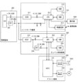
図2は、画像形成装置1の制御系統の説明図である。制御系統は、電源基板200、コントローラ基板210、エンジン制御基板220、及びドライバ基板230の4種類の基板を備える。
(control system)
FIG. 2 is an explanatory diagram of a control system of the image forming apparatus 1. As shown in FIG. The control system includes four types of boards: a
電源基板200は、所定の電圧値(本実施形態では+12[V])の2種類の電源電圧(本実施形態では+12V_CONT電源電圧、+12V_ENG電源電圧)を生成して出力する。+12V_CON電源電圧は、12[V]の電源から直接出力される。+12V_ENG電源電圧は、12[V]の電源からFET(Field Effect Transistor)201を介して出力される。+12V_CONT電源電圧は、コントローラ基板210等へ供給される。+12V_ENG電源電圧は、コントローラ基板210及びエンジン制御基板220等へ供給される。FET201は、保護素子として機能し、エンジン制御基板220側で異常が発生したときに、+12V_ENG電源の電源系統を介して、該異常が電源基板200に影響することを防止する。
The
コントローラ基板210は、CPU(Central Processing Unit)212、ROM(Read Only Memory)214、及びRAM(Random Access Memory)215を備える。また、コントローラ基板210は、DCDCコンバータ211及びNW通信部213を備える。DCDCコンバータ211は、電源基板200から供給される+12V_CON電源電圧を所定の電圧値(本実施形態では+3.3[V])の電圧(+3.3V_CON電圧)に変圧する。DCDCコンバータ211で生成された+3.3_CON電圧は、CPU212の動作に用いられる。CPU212は、ROM214に格納されたコンピュータプログラムを実行することで、エンジン制御基板220の動作を制御する。その際、RAM225は、ワークメモリとして用いられ、一時的又は恒久的に保存することが必要な書き換え可能なデータを格納する。NW通信部213は、LAN(Local Area Network)等の通信回線を介したコールセンタ等の外部装置との通信を制御する通信インタフェースである。CPU212は、NW通信部213を介して外部装置との間で通信を行う。CPU212は、操作部1000に接続され、操作部1000にメッセージ等を表示させる。また、CPU212は、操作部1000から指示等の入力を受け付ける。また、RAM215は、エンジン制御基板220が検知した異常を表す情報を記憶する。
The
エンジン制御基板220は、DCDCコンバータ221、CPU222、ROM223、RAM225、及びFET224を備える。DCDCコンバータ221は、電源基板200から供給される+12V_ENG電源電圧を所定の電圧値(本実施形態では+3.3[V])の電圧(+3.3V_ENG電圧)に変圧する。DCDCコンバータ221で生成された+3.3V_ENG電圧は、CPU222及びドライバ基板230の動作に用いられる。ドライバ基板230に供給される+3.3V_ENG電圧は、FET224を介して、+3.3V_DRV電圧として出力される。FET224は、保護素子として機能し、ドライバ基板230側で異常が発生したときに、+3.3V_ENG電源の電源系統を介して、該異常が電源基板200に影響することを防止する。CPU222は、+3.3V_ENG電圧により動作する。CPU222は、ROM223に格納されたコンピュータプログラム及びコントローラ基板210のCPU212の指示に応じてドライバ基板230の動作を制御する。その際、RAM225は、ワークメモリとして用いられ、一時的又は恒久的に保存することが必要な書き換え可能なデータを格納する。また、RAM225は、ドライバ基板230で発生した異常を表す情報を記憶する。
The
ドライバ基板230は、ASIC(Application Specific Integrated Circuit)231、センサ検知部232、及びモータ駆動部233を備える。センサ検知部232には、センサ2321が接続される。モータ駆動部233には、モータ2331が接続される。ASIC231は、エンジン制御基板220から供給される+3.3V_DRV電圧により動作する。ASIC231は、エンジン制御基板220のCPU222により、負荷(モータ2331)を駆動するタイミングを制御される。モータ駆動部233は、ASIC231の制御によりモータ2331を駆動する。モータ2331は、図1に示すロータリ現像ユニット13の回転、或いはシート搬送に用いられる。センサ検知部232は、センサ2321の検知結果を取得する。センサ2321は、図1に示すシートサイズの検知、或いはシートの有無の検知に用いられる。センサ検知部232は、取得したセンサ2321の検知結果をASIC231へ送信する。
The
+12V_ENG電源電圧は、電源基板200からエンジン制御基板220へ正常に供給されているか否かを判定できるように、コントローラ基板210のCPU212の定格範囲に収まるように分圧される。分圧された+12V_ENG電源電圧は、+12V_ENG電源検知信号としてコントローラ基板210のCPU212のアナログポートに入力される。CPU212は、+12V_ENG電源検知信号により、+12V_ENG電源電圧が電源基板200からエンジン制御基板220へ正常に供給されているか否かを判定する。本実施形態では、分圧後の電圧値を+3.3[V]とする。
The +12V_ENG power supply voltage is divided so that it falls within the rated range of the
+3.3V_DRV電圧も同様に、エンジン制御基板220からドライバ基板230へ正常に供給されているか否かを判定できるように、+3.3V_DRV電源検知信号としてエンジン制御基板220のCPU222のアナログポートに入力される。CPU222は、+3.3V_DRV電源検知信号により、+3.3V_DRV電圧がエンジン制御基板220からドライバ基板230へ正常に供給されているか否かを判定する。
Similarly, the +3.3V_DRV voltage is input to the analog port of the
なお、+12V_ENG電源電圧及び+3.3V_DRV電圧が正常に供給されているか否かを判定するための構成は、これに限らない。例えば、+12V_ENG電源電圧(+3.3V_DRV電圧)をトランジスタ等の検知回路によりデジタル値に変換して、CPU212(CPU222)のデジタルポートに入力するようにしてもよい。 Note that the configuration for determining whether the +12V_ENG power supply voltage and the +3.3V_DRV voltage are normally supplied is not limited to this. For example, the +12V_ENG power supply voltage (+3.3V_DRV voltage) may be converted into a digital value by a detection circuit such as a transistor and input to the digital port of the CPU 212 (CPU 222).
エンジン制御基板220のCPU222とドライバ基板230のASIC231とは、所定の通信路を介して通信する。CPU222は、ASIC231と通信することで、負荷(モータ2331)の駆動タイミングの制御を行う。また、CPU222は、ASIC231からセンサ2321の検知結果等の信号を取得する。
The
エンジン制御基板220のCPU222とコントローラ基板210のCPU212とは、所定の通信路を介して通信する。コントローラ基板210のCPU212は、操作部1000や通信回線を介して画像形成の開始指示を取得すると、エンジン制御基板220のCPU222に画像形成の開始指示があったことを通知する。エンジン制御基板220のCPU222は、コントローラ基板210のCPU212から画像形成の開始指示を取得して、ドライバ基板230の動作を制御して画像形成処理を行う。
The
エンジン制御基板220のCPU222は、ドライバ基板230で検知された異常をRAM225に保存する。また、エンジン制御基板220のCPU222は、コントローラ基板210のCPU212に異常の発生を通知する。コントローラ基板210のCPU212は、異常の発生が通知されると、操作部1000等によりユーザやサービスマンに異常の発生を報知する。また、CPU212は、NW通信部213により通信回線を介してコールセンタへ異常の発生を報知する。このように、画像形成装置1の設置場所にいるユーザやサービスマンの他に、コールセンタにいるサービスマンに対して、異常の発生が報知される。
The
(故障箇所の特定処理)
図3は、このような制御系統でコントローラ基板210のCPU212とエンジン制御基板220のCPU222との間で通信異常が発生した場合における、コントローラ基板210のCPU212が実行する故障箇所の特定処理を表すフローチャートである。この処理では、+12V_ENG電源電圧の異常の有無が判定され、異常が発生している場合に故障箇所が特定される。この処理は、画像形成装置1の起動時から繰り返し実行される。
(Specifying process of fault location)
FIG. 3 is a flow chart showing a process for identifying a failure location executed by the
CPU212は、エンジン制御基板220のCPU222との間で通信を開始する(S301)。例えば、CPU212は、エンジン制御基板220のCPU222に対して通信の開始を指示する。CPU212は、エンジン制御基板220のCPU222から通信開始の指示に対する応答の有無を判定する(S302)。応答がある場合(S302:Y)、CPU212は、電源基板200から+12V_ENG電源電圧が正常に出力され、画像形成装置1が正常に動作していると判定して処理を終了する。
The
応答が無い場合(S302:N)、CPU212は、エンジン制御基板220に供給される+12V_ENG電源電圧の電圧値が所定の閾値以上であるか否かを判定する(S303)。具体的には、CPU212は、+12V_ENG電源電圧から変換された+12V_ENG電源検知信号の値(+3.3[V])を閾値と比較する。本実施形態では、閾値は、例えば+2.0[V]である。
When there is no response (S302: N), the
+12V_ENG電源電圧の電圧値が閾値以上である場合(S303:Y)、CPU212は、+12V_ENG電源電圧が正常であると判定する。この場合、CPU212は、電源系統以外の構成部品に異常が発生していると判定して、電源異常以外の異常の診断を行う(S306)。電源異常以外の異常の診断の詳細は省略する。
When the voltage value of the +12V_ENG power supply voltage is equal to or higher than the threshold (S303: Y), the
+12V_ENG電源電圧の電圧値が閾値未満である場合(S303:N)、CPU212は、+12V_ENG電源電圧が異常、つまり電源基板200が故障していると判定する(S304)。
When the voltage value of the +12V_ENG power supply voltage is less than the threshold (S303: N), the
CPU212は、S304及びS306のいずれかの処理により判定した故障箇所を、操作部1000を用いて報知する(S305)。図4は、操作部1000に表示される故障箇所の報知例を示す図である。図4は、電源基板200が故障した場合を例示し、電源基板200の交換を促す表示を示している。また、CPU212は、NW通信部213により通信回線を介してサポートセンサへ故障箇所を報知する。故障箇所の報知により、故障箇所の特定処理が終了する。
The
図5は、エンジン制御基板220のCPU222とドライバ基板230のASIC231との間で通信異常が発生した場合における、エンジン制御基板220のCPU222が実行する故障箇所の特定処理を表すフローチャートである。この処理では、+3.3V_DRV電圧の異常の有無が判定され、異常が発生している場合に故障箇所が特定される。この処理は、図4の処理により電源基板200から+12V_ENG電源電圧が正常に出力され、画像形成装置1が正常に動作していると判定された場合に行われる。
FIG. 5 is a flow chart showing a process of specifying a failure location executed by the
CPU222は、ドライバ基板230のASIC231との間で通信を開始する(S401)。例えば、CPU222は、ドライバ基板230のASIC231に対して通信の開始を指示する。CPU222は、ドライバ基板230のASIC231から通信開始の指示に対する応答の有無を判定する(S402)。応答がある場合(S402:Y)、CPU222は、エンジン制御基板220から+3.3V_DRV電圧が正常に出力され、画像形成装置1が正常に動作していると判定して処理を終了する。
The
応答が無い場合(S402:N)、CPU222は、ドライバ基板230に供給される+3.3V_DRV電圧の電圧値が所定の閾値以上であるか否かを判定する(S403)。具体的には、CPU222は、+3.3V_DRV電圧から変換された+3.3V_DRV電源検知信号の値(+3.3[V])を閾値と比較する。本実施形態では、閾値は、例えば+2.0[V]である。
When there is no response (S402: N), the
+3.3V_DRV電圧の電圧値が閾値以上である場合(S403:Y)、CPU222は、+3.3V_DRV電圧が正常であると判定する。この場合、CPU222は、電源系統以外の構成部品に異常が発生していると判定して、電源異常以外の異常の診断を行う(S406)。電源異常以外の異常の診断の詳細は省略する。
When the voltage value of the +3.3V_DRV voltage is equal to or greater than the threshold (S403: Y), the
+3.3V_DRV電圧の電圧値が閾値未満である場合(S403:N)、CPU222は、DCDCコンバータ221からFET224を介してドライバ基板230へ供給される+3.3V_DRV電圧が異常であると判定する。つまりCPU222は、エンジン制御基板220が故障していると判定する(S404)。CPU222は、S404及びS406のいずれかの処理により判定した故障箇所を、診断結果としてコントローラ基板210のCPU212へ送信する(S405)。
When the voltage value of the +3.3V_DRV voltage is less than the threshold (S403: N), the
図6は、コントローラ基板210のCPU212による、エンジン制御基板220のCPU222からの診断結果の取得処理を表すフローチャートである。この処理は、図5のS405の処理に応じた処理である。
FIG. 6 is a flow chart showing a process of acquiring diagnostic results from the
CPU212は、図5のS405の処理によりエンジン制御基板220のCPU222から送信される診断結果を取得したか否かを判定する(S501)。診断結果を取得した場合(S501:Y)、CPU212は、取得した診断結果が表す故障箇所を、操作部1000を用いて報知する(S502)。また、CPU212は、NW通信部213により通信回線を介してサポートセンサへ故障箇所を報知する。
The
以上のような本実施形態の画像形成装置1は、内部の基板間の通信に異常が発生したときに、異常の原因が電源系統であるか否かを判定する。電源系統である場合には、画像形成装置1は異常が発生している具体的な電源系統上の基板を特定する。これにより、サービスマンによる基板の交換作業にかかわるトータルの作業時間を低減することができる。 The image forming apparatus 1 of the present embodiment as described above determines whether or not the cause of the abnormality is the power supply system when an abnormality occurs in communication between internal boards. If it is the power supply system, the image forming apparatus 1 identifies a specific board on the power supply system in which the abnormality has occurred. As a result, it is possible to reduce the total work time involved in the board replacement work by service personnel.
Claims (11)
前記電源基板から出力される前記第1電源電圧により動作する第1制御手段を有する第1基板と、
前記電源基板から出力される前記第2電源電圧により動作する第2制御手段を有し、かつ前記第2電源電圧から第3電源電圧を生成する第2基板と、
前記第2基板から出力される前記第3電源電圧により動作する第3基板と、を備え、
前記第2基板の前記第2制御手段は、前記第3基板と通信を正常に行えるか否かを判定し、正常に行えない場合に前記第3電源電圧と所定の閾値とを比較した結果に応じて前記第2基板が異常であるか否かを判定することを特徴とする、
画像形成装置。 a power supply board that outputs a first power supply voltage and a second power supply voltage;
a first substrate having first control means operated by the first power supply voltage output from the power substrate;
a second substrate having second control means operated by the second power supply voltage output from the power supply substrate and generating a third power supply voltage from the second power supply voltage;
a third substrate operated by the third power supply voltage output from the second substrate;
The second control means of the second board determines whether or not communication with the third board can be performed normally, and if communication cannot be performed normally, the result of comparing the third power supply voltage and a predetermined threshold is determined. characterized by determining whether the second substrate is abnormal according to
Image forming device.
請求項1記載の画像形成装置。 The second control means for the second substrate determines that the second substrate is abnormal when the third power supply voltage is less than the predetermined threshold,
The image forming apparatus according to claim 1.
前記第2基板は、前記第3電源電圧を、第2保護素子を介して出力することを特徴とする、
請求項1又は2記載の画像形成装置。 The power supply substrate outputs the second power supply voltage through a first protection element,
The second substrate outputs the third power supply voltage via a second protection element,
3. The image forming apparatus according to claim 1.
請求項3記載の画像形成装置。 The first protection element and the second protection element are FETs,
4. The image forming apparatus according to claim 3.
前記第2基板の前記第2制御手段は、前記第1基板の前記第1制御手段が前記第2基板の前記第2制御手段と通信を正常に行えると判定した場合に、前記第3基板と通信を正常に行えるか否かを判定することを特徴とする、
請求項1乃至4の何れか1項記載の画像形成装置。 The first control means of the first board determines whether or not communication with the second control means of the second board can be performed normally,
The second control means of the second board communicates with the third board when it is determined that the first control means of the first board can normally communicate with the second control means of the second board. Characterized by determining whether communication can be performed normally,
The image forming apparatus according to any one of claims 1 to 4.
請求項5記載の画像形成装置。 When the first control means of the first substrate cannot communicate normally with the second control means of the second substrate, the above-described Characterized by determining whether the power supply board is abnormal,
6. The image forming apparatus according to claim 5.
請求項6記載の画像形成装置。 It further comprises a notification means for notifying the abnormality of the power supply board determined by the first control means and the abnormality of the second board determined by the second control means,
7. The image forming apparatus according to claim 6.
請求項7記載の画像形成装置。 The notification means notifies the abnormality of the power supply substrate and the abnormality of the second substrate by displaying on a predetermined display,
The image forming apparatus according to claim 7.
請求項7記載の画像形成装置。 The notification means notifies an external device of the abnormality of the power supply board and the abnormality of the second board via a communication line,
The image forming apparatus according to claim 7.
請求項1乃至9の何れか1項記載の画像形成装置。 The first control means determines whether or not communication with the second board can be performed normally, and if the communication with the second board cannot be performed normally, the second power supply voltage and the second predetermined voltage Determining whether the power supply board is abnormal according to the result of comparing with the threshold,
The image forming apparatus according to any one of claims 1 to 9.
請求項10記載の画像形成装置。 The first control means determines that the power supply substrate is abnormal when the second power supply voltage is less than the second predetermined threshold,
The image forming apparatus according to claim 10.
Priority Applications (1)
| Application Number | Priority Date | Filing Date | Title |
|---|---|---|---|
| JP2018208313A JP7301520B2 (en) | 2018-11-05 | 2018-11-05 | image forming device |
Applications Claiming Priority (1)
| Application Number | Priority Date | Filing Date | Title |
|---|---|---|---|
| JP2018208313A JP7301520B2 (en) | 2018-11-05 | 2018-11-05 | image forming device |
Publications (3)
| Publication Number | Publication Date |
|---|---|
| JP2020076803A JP2020076803A (en) | 2020-05-21 |
| JP2020076803A5 JP2020076803A5 (en) | 2021-11-25 |
| JP7301520B2 true JP7301520B2 (en) | 2023-07-03 |
Family
ID=70723983
Family Applications (1)
| Application Number | Title | Priority Date | Filing Date |
|---|---|---|---|
| JP2018208313A Active JP7301520B2 (en) | 2018-11-05 | 2018-11-05 | image forming device |
Country Status (1)
| Country | Link |
|---|---|
| JP (1) | JP7301520B2 (en) |
Citations (3)
| Publication number | Priority date | Publication date | Assignee | Title |
|---|---|---|---|---|
| JP2005266314A (en) | 2004-03-18 | 2005-09-29 | Fuji Xerox Co Ltd | Multifunction machine and control method therefor |
| JP2007060817A (en) | 2005-08-25 | 2007-03-08 | Fuji Xerox Co Ltd | Power supply unit |
| JP2011209538A (en) | 2010-03-30 | 2011-10-20 | Kyocera Mita Corp | Image forming device |
Family Cites Families (1)
| Publication number | Priority date | Publication date | Assignee | Title |
|---|---|---|---|---|
| JPH1117863A (en) * | 1997-06-20 | 1999-01-22 | Canon Inc | Picture forming device |
-
2018
- 2018-11-05 JP JP2018208313A patent/JP7301520B2/en active Active
Patent Citations (3)
| Publication number | Priority date | Publication date | Assignee | Title |
|---|---|---|---|---|
| JP2005266314A (en) | 2004-03-18 | 2005-09-29 | Fuji Xerox Co Ltd | Multifunction machine and control method therefor |
| JP2007060817A (en) | 2005-08-25 | 2007-03-08 | Fuji Xerox Co Ltd | Power supply unit |
| JP2011209538A (en) | 2010-03-30 | 2011-10-20 | Kyocera Mita Corp | Image forming device |
Also Published As
| Publication number | Publication date |
|---|---|
| JP2020076803A (en) | 2020-05-21 |
Similar Documents
| Publication | Publication Date | Title |
|---|---|---|
| JP7229727B2 (en) | image forming device | |
| JP2007172127A (en) | Simulation system, simulation device, image forming device, simulation method, program and storage medium | |
| US11245797B2 (en) | Image forming apparatus, malfunction diagnosis method of image forming apparatus, and storage medium | |
| US11184487B2 (en) | Image forming apparatus | |
| JP2023165809A (en) | Image forming apparatus and method for controlling the same | |
| US20170017449A1 (en) | Image forming apparatus, server, and non-transitory computer readable medium | |
| JP7301520B2 (en) | image forming device | |
| US11102358B2 (en) | Image forming apparatus determining failure when reactivated before preparing a printing operation | |
| US10996604B2 (en) | Image forming apparatus configured to diagnose failure | |
| JP6558295B2 (en) | Image forming apparatus | |
| US20200120217A1 (en) | Image forming apparatus, abnormal member detection method and non-transitory computer-readable recording medium encoded with abnormal member detection program | |
| JP7475837B2 (en) | Image forming device | |
| US10795300B2 (en) | Image forming apparatus | |
| JP2007140044A (en) | Image forming apparatus | |
| JP2021020347A (en) | Image formation apparatus | |
| JP2021009225A (en) | Image forming apparatus | |
| JP2020076840A (en) | Image formation device, and fault site identifying method | |
| US11316985B2 (en) | Image forming apparatus for determining whether a door sensor or an interrupt voltage switch has failed | |
| JP2021081584A (en) | Image forming apparatus and method for controlling the same | |
| JP2006259353A (en) | Image forming apparatus | |
| JPS5866967A (en) | Trouble diagnosing device for copying machine | |
| JPH1026913A (en) | Image forming device | |
| JP2020173376A (en) | Image forming apparatus | |
| JP2010145935A (en) | Image forming apparatus, driving method of transfer material, and computer program | |
| KR20000019775A (en) | Method for cleaning image forming apparatus |
Legal Events
| Date | Code | Title | Description |
|---|---|---|---|
| A521 | Request for written amendment filed |
Free format text: JAPANESE INTERMEDIATE CODE: A523 Effective date: 20211015 |
|
| A621 | Written request for application examination |
Free format text: JAPANESE INTERMEDIATE CODE: A621 Effective date: 20211015 |
|
| A977 | Report on retrieval |
Free format text: JAPANESE INTERMEDIATE CODE: A971007 Effective date: 20220810 |
|
| A131 | Notification of reasons for refusal |
Free format text: JAPANESE INTERMEDIATE CODE: A131 Effective date: 20220906 |
|
| A521 | Request for written amendment filed |
Free format text: JAPANESE INTERMEDIATE CODE: A523 Effective date: 20221102 |
|
| A131 | Notification of reasons for refusal |
Free format text: JAPANESE INTERMEDIATE CODE: A131 Effective date: 20230124 |
|
| A521 | Request for written amendment filed |
Free format text: JAPANESE INTERMEDIATE CODE: A523 Effective date: 20230315 |
|
| TRDD | Decision of grant or rejection written | ||
| A01 | Written decision to grant a patent or to grant a registration (utility model) |
Free format text: JAPANESE INTERMEDIATE CODE: A01 Effective date: 20230523 |
|
| A61 | First payment of annual fees (during grant procedure) |
Free format text: JAPANESE INTERMEDIATE CODE: A61 Effective date: 20230621 |
|
| R151 | Written notification of patent or utility model registration |
Ref document number: 7301520 Country of ref document: JP Free format text: JAPANESE INTERMEDIATE CODE: R151 |