JP7272430B2 - Battery packs and electrical equipment - Google Patents

Battery packs and electrical equipment Download PDF

Info

Publication number
JP7272430B2
JP7272430B2 JP2021522222A JP2021522222A JP7272430B2 JP 7272430 B2 JP7272430 B2 JP 7272430B2 JP 2021522222 A JP2021522222 A JP 2021522222A JP 2021522222 A JP2021522222 A JP 2021522222A JP 7272430 B2 JP7272430 B2 JP 7272430B2
Authority
JP
Japan
Prior art keywords
circuit board
terminal
battery pack
battery
wireless communication
Prior art date
Legal status (The legal status is an assumption and is not a legal conclusion. Google has not performed a legal analysis and makes no representation as to the accuracy of the status listed.)
Active
Application number
JP2021522222A
Other languages
Japanese (ja)
Other versions
JPWO2020241327A1 (en
JPWO2020241327A5 (en
Inventor
聡明 増森
聡史 山口
浩之 塙
Current Assignee (The listed assignees may be inaccurate. Google has not performed a legal analysis and makes no representation or warranty as to the accuracy of the list.)
Koki Holdings Co Ltd
Original Assignee
Koki Holdings Co Ltd
Priority date (The priority date is an assumption and is not a legal conclusion. Google has not performed a legal analysis and makes no representation as to the accuracy of the date listed.)
Filing date
Publication date
Application filed by Koki Holdings Co Ltd filed Critical Koki Holdings Co Ltd
Publication of JPWO2020241327A1 publication Critical patent/JPWO2020241327A1/ja
Publication of JPWO2020241327A5 publication Critical patent/JPWO2020241327A5/ja
Application granted granted Critical
Publication of JP7272430B2 publication Critical patent/JP7272430B2/en
Active legal-status Critical Current
Anticipated expiration legal-status Critical

Links

Images

Classifications

    • BPERFORMING OPERATIONS; TRANSPORTING
    • B25HAND TOOLS; PORTABLE POWER-DRIVEN TOOLS; MANIPULATORS
    • B25FCOMBINATION OR MULTI-PURPOSE TOOLS NOT OTHERWISE PROVIDED FOR; DETAILS OR COMPONENTS OF PORTABLE POWER-DRIVEN TOOLS NOT PARTICULARLY RELATED TO THE OPERATIONS PERFORMED AND NOT OTHERWISE PROVIDED FOR
    • B25F5/00Details or components of portable power-driven tools not particularly related to the operations performed and not otherwise provided for
    • YGENERAL TAGGING OF NEW TECHNOLOGICAL DEVELOPMENTS; GENERAL TAGGING OF CROSS-SECTIONAL TECHNOLOGIES SPANNING OVER SEVERAL SECTIONS OF THE IPC; TECHNICAL SUBJECTS COVERED BY FORMER USPC CROSS-REFERENCE ART COLLECTIONS [XRACs] AND DIGESTS
    • Y02TECHNOLOGIES OR APPLICATIONS FOR MITIGATION OR ADAPTATION AGAINST CLIMATE CHANGE
    • Y02EREDUCTION OF GREENHOUSE GAS [GHG] EMISSIONS, RELATED TO ENERGY GENERATION, TRANSMISSION OR DISTRIBUTION
    • Y02E60/00Enabling technologies; Technologies with a potential or indirect contribution to GHG emissions mitigation
    • Y02E60/10Energy storage using batteries

Landscapes

  • Engineering & Computer Science (AREA)
  • Mechanical Engineering (AREA)
  • Battery Mounting, Suspending (AREA)

Description

本発明は無線通信機能付きの電池パックに関するものである。 The present invention relates to a battery pack with wireless communication function.

特許文献1では、電気機器の利便性を高めるために、電気機器の使用履歴情報を、通信部を有するアダプタを介して外部機器へ送信することが開示されている。 Patent Literature 1 discloses transmitting usage history information of an electrical device to an external device via an adapter having a communication unit in order to improve convenience of the electrical device.

特開2019-25611号公報JP 2019-25611 A

さらに電気機器の利便性を高めるため、発明者らは電池パックに無線通信機構を搭載することを考えた。電池パックの内部に無線通信機能を実装する場合、一番問題となるのはアンテナの設置位置である。使用する無線周波数の特性から、金属端子の付近や、基板の配線パターン部分を可能な限り避けた位置にアンテナを配置する必要がある。また、基板に搭載された電子素子やモジュール等の発熱を抑えるために、基板における主要なパワーラインから可能な限り遠ざけることが好ましい。 Furthermore, in order to improve the convenience of electrical equipment, the inventors considered mounting a wireless communication mechanism on the battery pack. When implementing a wireless communication function inside a battery pack, the biggest problem is the installation position of the antenna. Due to the characteristics of the radio frequency used, it is necessary to place the antenna in the vicinity of metal terminals and in a position that avoids the wiring pattern portion of the board as much as possible. Also, in order to suppress heat generation by electronic elements, modules, etc. mounted on the board, it is preferable to keep them as far away from the main power lines on the board as possible.

本発明は上記背景に鑑みてなされたものであって、本発明の目的は、無線通信部を最適な位置に搭載した電池パックを提供することにある。本発明の他の目的は、無線通信部の防塵、防水を効果的に達成できる電池パックを提供することにある。本発明のさらに他の目的は、無線通信部を搭載した基板の組み立て効率を向上させた電池パックを提供することにある。 The present invention has been made in view of the above background, and an object of the present invention is to provide a battery pack in which a wireless communication section is mounted at an optimum position. Another object of the present invention is to provide a battery pack that can effectively achieve dustproof and waterproof protection of the wireless communication unit. Still another object of the present invention is to provide a battery pack in which the efficiency of assembling a board on which a wireless communication section is mounted is improved.

本願において開示される発明のうち代表的な特徴を説明すれば次のとおりである。
本発明の一つの特徴によれば、複数の電池セルと、電池セルに接続される正極端子及び負極端子を含む接続端子群と、電池セルの制御回路を搭載する回路基板と、を有する電池パックであって、、正極端子は回路基板の左右方向の一方側に配置され、負極端子は回路基板の左右方向の他方側に配置され、回路基板の接続端子群を基準にした前後方向の一方側に制御回路を搭載する。また、回路基板の接続端子群を基準にした前後方向の他方側に外部機器との無線通信を行うための無線通信部を搭載する。回路基板の接続端子群の前後方向の他方側の領域を左右方向に3分割した際、左右両側の領域内に電池セルの正極端子及び負極端子が接続される接続タブをそれぞれ配置し、中央の領域内に無線通信部を搭載する。また、回路基板は、電池セルを覆うように設けられ、上面視において略四角形であり、正極端子及び負極端子は左右方向に離間して回路基板に固定される。無線通信部は回路基板の前後方向の他方の端部に配置される
The typical features of the invention disclosed in the present application are as follows.
According to one aspect of the present invention, a battery pack includes a plurality of battery cells, a connection terminal group including a positive terminal and a negative terminal connected to the battery cells, and a circuit board on which a control circuit for the battery cells is mounted. The positive terminal is arranged on one side of the circuit board in the horizontal direction, and the negative terminal is arranged on the other side of the circuit board in the horizontal direction. Equipped with a control circuit. Also, a wireless communication unit for performing wireless communication with an external device is mounted on the other side in the front-rear direction with reference to the connection terminal group of the circuit board. When the area on the other side of the connection terminal group in the front-rear direction of the circuit board is divided in the left-right direction into three areas, the connection tabs to which the positive terminal and the negative terminal of the battery cell are connected are arranged in the left and right areas, respectively. A wireless communication unit is installed within the area. Moreover, the circuit board is provided so as to cover the battery cells, and has a substantially rectangular shape when viewed from above, and the positive terminal and the negative terminal are fixed to the circuit board while being spaced apart in the left-right direction. The wireless communication unit is arranged at the other end of the circuit board in the front-rear direction .

本発明の他の特徴によれば、複数の電池セルの軸線がそれぞれ平行となるように、隣接するセルの向きを交互に横方向に並べて保持する非導電性のセパレータを有し、回路基板はセパレータの上側に配置され、回路基板の前側の角部に直列接続される電池セルの一つの接続タブが配線され、無線通信部は、接続タブとは離れた位置に配置される。また、複数の電池セルが複数本ずつ直列接続されて構成される第1セルユニットと、複数の電池セルが複数本ずつ直列接続されて構成される第2セルユニットを有し、回路基板の前側の2つの角部にはそれぞれ、第1セルユニットの接続タブと第2セルユニットの接続タブが配置され、回路基板の後側の2つの角部にはそれぞれ、第1セルユニットの接続タブと第2セルユニットの接続タブが配置され、無線通信部は、回路基板の前側に配置された2つの接続タブの間に配置される。さらに、無線通信部は、無線通信回路を内蔵するマイコンと、マイコンに接続されるアンテナ部を含んで構成され、アンテナ部は、マイコンよりも装着方向の前側に配置される。 According to another aspect of the invention, the circuit board has non-conductive separators for holding adjacent cells in alternating lateral orientations such that the axes of the plurality of battery cells are parallel to each other; A connection tab of one of the series-connected battery cells is arranged on the upper side of the separator and is wired to the front corner of the circuit board, and the wireless communication section is arranged at a position separated from the connection tab. The front side of the circuit board has a first cell unit configured by connecting a plurality of battery cells in series and a second cell unit configured by connecting a plurality of battery cells in series. The connection tabs of the first cell unit and the connection tabs of the second cell unit are respectively arranged at the two corners of the circuit board, and the connection tabs of the first cell unit and the connection tabs of the first cell unit are arranged at the two corners of the rear side of the circuit board. A connection tab of the second cell unit is arranged, and the wireless communication part is arranged between two connection tabs arranged on the front side of the circuit board. Further, the radio communication section includes a microcomputer containing a radio communication circuit and an antenna section connected to the microcomputer, and the antenna section is arranged in front of the microcomputer in the mounting direction.

本発明のさらに他の特徴によれば、アンテナ部とマイコンは共通のベース部材にあらかじめ搭載され、マイコンの端子群が回路基板にハンダ付けされることによってベース部材が回路基板に固定される。また、マイコンは回路基板の左右中心線を通る位置に配置される。制御回路には、電池保護用のICが含まれる。 According to still another feature of the present invention, the antenna section and the microcomputer are preliminarily mounted on a common base member, and the base member is fixed to the circuit board by soldering terminals of the microcomputer to the circuit board. Also, the microcomputer is arranged at a position passing through the left-right center line of the circuit board. The control circuit includes an IC for battery protection.

本発明のさらに他の特徴によれば、複数の電池セルと、電池セルに接続される正極端子及び負極端子を含む接続端子群と、電池セルの制御回路を搭載する回路基板と、を有する電池パックであって、正極端子は回路基板の左右方向の一方側に配置され、負極端子は回路基板の左右方向の他方側に配置され、回路基板の接続端子群を基準にした前後方向に見て前側の端部であって、左右中心線を通る位置に、外部機器との無線通信を行うためのマイコンと、マイコンと接続されるアンテナ部を搭載し、回路基板の接続端子群の前側領域を左右方向に3分割した際に、左右両側の領域内に電池セルからの接続タブをそれぞれ配置し、中央の領域内にマイコンを搭載した。アンテナ部は、マイコンよりも前後方向の前側に配置される。 According to still another feature of the present invention, a battery includes a plurality of battery cells, a connection terminal group including a positive electrode terminal and a negative electrode terminal connected to the battery cells, and a circuit board on which a control circuit for the battery cells is mounted. In the pack, the positive terminal is arranged on one side of the circuit board in the left-right direction, and the negative terminal is arranged on the other side of the circuit board in the left-right direction. A microcomputer for wireless communication with external devices and an antenna connected to the microcomputer are mounted at the front end, passing through the left-right center line. When it is divided into three parts in the horizontal direction, connection tabs from the battery cells are arranged in the left and right regions, respectively, and a microcomputer is mounted in the central region. The antenna section is arranged in front of the microcomputer in the front-rear direction.

本発明によれば、電池パックの回路基板上の特定の位置に無線通信部を搭載したので、金属端子の付近、基板裏を可能な限り避けた配置を実現でき、電波の特性からもアンテナ効率の低下を抑えることが可能となった。また、基板における主要なパワーラインから可能な限り遠ざけることができたので、無線通信部への熱の影響を抑えることが可能となった。さらに、従来の回路基板自体の形状を変更することなく無線通信機能を搭載可能にしたので、無線通信機能を搭載することによる電池パックの製造コストの上昇を抑えることができ、従来の組み立て手順とほぼ同様に製造可能である。 According to the present invention, since the wireless communication section is mounted at a specific position on the circuit board of the battery pack, it is possible to avoid the vicinity of the metal terminals and the back of the board as much as possible. It became possible to suppress the decrease in In addition, since it was possible to keep it as far away from the main power lines on the board as possible, it was possible to suppress the influence of heat on the wireless communication section. Furthermore, since the wireless communication function can be mounted without changing the shape of the conventional circuit board itself, it is possible to suppress the increase in the manufacturing cost of the battery pack due to the mounting of the wireless communication function. It can be manufactured in almost the same way.

本発明の実施例にかかる電池パック100を用いた管理システムの全体概略図である。1 is an overall schematic diagram of a management system using a battery pack 100 according to an embodiment of the present invention; FIG. 本発明の実施例に係る電池パック100の斜視図である。1 is a perspective view of a battery pack 100 according to an embodiment of the invention; FIG. 本発明に係る電池パック100が装着される電動工具本体1の斜視図である。1 is a perspective view of a power tool main body 1 to which a battery pack 100 according to the present invention is attached; FIG. 図3の電池パック100の展開斜視図である。FIG. 4 is an exploded perspective view of the battery pack 100 of FIG. 3; (A)は電池パック100の正極端子(162と172)、負極端子(167と177)の形状を示す部分斜視図と高電圧出力時の接続回路を示す図であり、(B)は高電圧電気機器のターミナル部50と、電池パック100側の端子との接続状況を示すための部分斜視図である。(A) is a partial perspective view showing the shapes of the positive terminals (162 and 172) and the negative terminals (167 and 177) of the battery pack 100, and a diagram showing a connection circuit when a high voltage is output; FIG. 3 is a partial perspective view showing a state of connection between a terminal portion 50 of an electrical device and a terminal on the battery pack 100 side; (A)は電池パック100の正極端子(162と172)、負極端子(167と177)の形状を示す部分斜視図と低電圧出力時の接続回路を示す図であり、(B)は低電圧電気機器のターミナル部80と、電池パック100側の端子との接続状況を示すための部分斜視図である。(A) is a partial perspective view showing the shapes of positive terminals (162 and 172) and negative terminals (167 and 177) of the battery pack 100, and a diagram showing a connection circuit when outputting a low voltage; FIG. 3 is a partial perspective view showing a state of connection between a terminal portion 80 of an electrical device and a terminal on the battery pack 100 side; 図4のセパレータ245を用いた電池セルのスタック状況および配線方法を説明するための展開斜視図である。FIG. 5 is an exploded perspective view for explaining a stacking state and a wiring method of battery cells using the separator 245 of FIG. 4; 電池パック100の基本的な内部回路を示すブロック図である。2 is a block diagram showing a basic internal circuit of battery pack 100. FIG. 電圧自動切替式の電池パック100を接続する高電圧用の電気機器の回路図である。1 is a circuit diagram of a high-voltage electrical device to which an automatic voltage switching type battery pack 100 is connected; FIG. 図5の部品を組み立てた後のセパレータ245の側面図であり、(A)は右側面であり、(B)は左側面図である。FIG. 6 is a side view of the separator 245 after assembling the parts of FIG. 5, where (A) is the right side and (B) is the left side view; セパレータ245に回路基板150を固定した状態を示す斜視図である(左前上方より見た斜視図)。FIG. 11 is a perspective view showing a state in which the circuit board 150 is fixed to the separator 245 (perspective view seen from the upper front left); セパレータ245に回路基板150を固定した状態を示す斜視図である(右後上方より見た斜視図)。FIG. 11 is a perspective view showing a state in which the circuit board 150 is fixed to the separator 245 (perspective view seen from the upper rear right). 図16は電池パック100の 引出し板261、266、271、276と正極端子(162、172)及び負極端子(167、177)への接続方法を説明するための図である。FIG. 16 is a diagram for explaining how to connect the drawer plates 261, 266, 271, 276 of the battery pack 100 to the positive terminals (162, 172) and the negative terminals (167, 177). 本発明に係る電池パック100の回路基板150の上面図である。4 is a top view of the circuit board 150 of the battery pack 100 according to the present invention; FIG. 図14の回路基板150のうち、無線通信用のモジュールを取り外した状態を示す上面図である。15 is a top view showing a state in which a wireless communication module is removed from the circuit board 150 of FIG. 14; FIG. 図14の電池パック100の回路基板150のA-A断面図である。FIG. 15 is a cross-sectional view of the circuit board 150 of the battery pack 100 of FIG. 14 taken along the line AA. 図14の電池パック100の回路基板150の正面図である。FIG. 15 is a front view of a circuit board 150 of the battery pack 100 of FIG. 14; 本発明に係る電池パック100の回路基板150へのシリコン塗布状況を示す図である。FIG. 4 is a diagram showing the state of silicon application to the circuit board 150 of the battery pack 100 according to the present invention; 図18の型枠281の斜視図である。Fig. 19 is a perspective view of the mold 281 of Fig. 18; 図18とは別の方法による回路基板150へのシリコン塗布状況を示す図である。FIG. 19 is a diagram showing a state of applying silicon to the circuit board 150 by a method different from that of FIG. 18;

以下、本発明の実施例を図面に基づいて説明する。以下の図において、同一の部分には同一の符号を付し、繰り返しの説明は省略する。本明細書においては、電気機器の一例として電池パックにて動作する電動工具を用いて説明するものとする。 Embodiments of the present invention will be described below with reference to the drawings. In the following figures, the same parts are denoted by the same reference numerals, and repeated descriptions are omitted. In this specification, an electric power tool operated by a battery pack is used as an example of an electric device.

図1は本発明の実施例にかかる電池パック100を用いた管理システムの全体概略図である。電動工具本体1は、電池パック100-1を電源として使用可能な携帯型の電気機器であって、従来から広く用いられるインパクト工具である。本実施例の電池パック100は、内部にマイコンが搭載され、そのマイコンとの近接無線通信を可能とするブルートゥース(Bluetooth:Bluetooth SIG, Inc. USAの登録商標)が搭載される。このように電池パック100の内部に無線通信装置が搭載されるため、外部機器たる端末装置301との電池パック100-1~3の間での双方向に無線通信が可能となる。端末装置301は、電動工具本体1に装着されている状態の電池パック100-1との通信も可能であるし、電動工具本体1等の電気機器から取り外した状態の電池パック100-2、100-3とも通信が可能である。 FIG. 1 is an overall schematic diagram of a management system using a battery pack 100 according to an embodiment of the present invention. The power tool main body 1 is a portable electric device that can use the battery pack 100-1 as a power source, and is an impact tool that has been widely used in the past. The battery pack 100 of this embodiment incorporates a microcomputer and Bluetooth (registered trademark of Bluetooth SIG, Inc. USA) that enables close proximity wireless communication with the microcomputer. Since the wireless communication device is mounted inside the battery pack 100 in this manner, bi-directional wireless communication between the battery packs 100-1 to 100-3 with the terminal device 301, which is an external device, becomes possible. The terminal device 301 can also communicate with the battery pack 100-1 attached to the power tool main body 1, and can communicate with the battery packs 100-2 and 100 removed from the electric device such as the power tool main body 1. -3 can also communicate.

電池パック100-1~nは、定格電圧3.6Vのリチウムイオン電池セルを複数本直列接続して、例えば18V又は36Vの直流電流を選択的に出力可能としたものである。電池パック100が装着される側の電動工具(図示せず)には、ブルートゥース(登録商標)が設けられている機種も存在する。その場合は、端末装置301が電動工具と接続することによって、端末装置301が電池パック100の情報を間接的に取得することも可能な場合もある。しかしながら、本実施例では電池パック100と端末装置301が直接通信を行うことによって、どんな電動工具に装着されている電池パック100であっても、また、電動工具から取り外された状態の電池パック100であっても、端末装置301は電池パック100の情報を読み取ることが可能である。 Each of the battery packs 100-1 to 100-n is configured by connecting a plurality of lithium ion battery cells with a rated voltage of 3.6V in series so as to selectively output a DC current of 18V or 36V, for example. Some electric tools (not shown) to which the battery pack 100 is attached are equipped with Bluetooth (registered trademark). In that case, it may be possible for the terminal device 301 to indirectly acquire the information of the battery pack 100 by connecting the terminal device 301 to the power tool. However, in this embodiment, the battery pack 100 and the terminal device 301 directly communicate with each other, so that the battery pack 100 attached to any power tool can be used even when the battery pack 100 is removed from the power tool. However, the terminal device 301 can read the information of the battery pack 100 .

電池パック100-1~3は、ここでは同一型式、同一容量の電池パックとしているが、同一の電池パック100だけに限られず、異なる形式の様々な電圧、容量の電池パックでも良い。但し、それぞれの電池パック100内には電池の管理を行うプロセッサと無線通信装置を有することが重要である。端末装置301は、例えば電話会社が販売するスマートフォンを用いることができる。端末装置301は、電話通信網361を用いて電話会社の基地局360に接続可能であり、インターネット等のネットワーク350を用いて、電池パック100の製造メーカーや、サポート会社300のサーバ装置に接続可能である。よって、端末装置301は電池パック100-1~3から受信した情報をサポート会社300のサーバ装置に送信することが可能であり、また、端末装置301から何らかの情報を受信して表示画面302に表示することができる。さらには、無線通信装置を用いて特定の電池パック(例えば100-2)と無線通信を行い、電池パック100-2のマイコンに情報を書き込むことが可能である。 Although the battery packs 100-1 to 100-3 have the same model and the same capacity here, they are not limited to the same battery pack 100, and may be different types of battery packs with various voltages and capacities. However, it is important that each battery pack 100 has a processor for battery management and a wireless communication device. For the terminal device 301, for example, a smart phone sold by a telephone company can be used. The terminal device 301 can be connected to a base station 360 of a telephone company using a telephone communication network 361, and can be connected to a server device of a manufacturer of the battery pack 100 and a support company 300 using a network 350 such as the Internet. is. Therefore, the terminal device 301 can transmit the information received from the battery packs 100-1 to 100-3 to the server device of the support company 300, and receive some information from the terminal device 301 and display it on the display screen 302. can do. Furthermore, it is possible to perform wireless communication with a specific battery pack (for example, 100-2) using a wireless communication device and write information to the microcomputer of battery pack 100-2.

電池パック100(例えば100-1)は端末装置301とペアリングを行う。「ペアリング」とは、無線通信を用いて端末装置301と、電池パック100側の関連づけ登録を行う作業であり、これらの登録作業(ペアリング)を行うことにより、端末装置301は、ペアリングされた電池パック100から必要な情報を取得することができる。このペアリング相手の関係は、端末装置:電池パックの数=1:1でも良いが、図のように1:n(nは自然数)であっても良い。nがいくつまでペアリングできるかは、使用する無線通信規格に依存する。また、所有するすべての無線接続可能な電池パックと同時にペアリングさせても良いが、必ずしも全数を同時に行う必要は無く、状態を確認したい対象の電池パック100だけを選択してペアリングさせるようにしても良い。 The battery pack 100 (eg 100-1) performs pairing with the terminal device 301. FIG. “Pairing” is a task of performing association registration between the terminal device 301 and the battery pack 100 side using wireless communication. Necessary information can be acquired from the battery pack 100 that has been stored. This pairing partner relationship may be terminal device:number of battery packs=1:1, or may be 1:n (n is a natural number) as shown in the figure. How many n can be paired depends on the wireless communication standard used. In addition, it is possible to perform pairing simultaneously with all of the owned battery packs that can be wirelessly connected, but it is not necessary to perform all of them at the same time. can be

端末装置301は、電池パック100から無線通信によって受信した情報を処理し、電池パック100の状態、特に充電回数、過充電回数、過放電回数、装着した電動工具の種類や、使用時の電圧記録の各種使用状況を取得し、電池パック100の現在の状態を把握する。把握された情報は電話通信網361、ネットワーク350を介してサポート会社300にそのデータが送信される。端末装置301には、電池パック100との無線通信を可能とするために、専用のソフトウェア、いわゆるアプリケーションソフトをインストールしておく。なお、端末装置301は、いわゆるスマートフォンだけに限定されず、電池パック100側の無線通信装置と双方向または片方向の無線通信が可能であれば、タブレット型のPC(Personal Computer)や、汎用のPC等であっても良い。 The terminal device 301 processes information received from the battery pack 100 by wireless communication, and records the state of the battery pack 100, especially the number of times of charging, the number of overcharging, the number of overdischarging, the type of electric tool attached, and the voltage record during use. , and grasps the current state of the battery pack 100 . The grasped information is transmitted to the support company 300 via the telephone communication network 361 and network 350 . Dedicated software, so-called application software, is installed in the terminal device 301 in order to enable wireless communication with the battery pack 100 . Note that the terminal device 301 is not limited to a so-called smartphone, and may be a tablet PC (Personal Computer) or a general-purpose computer as long as it is capable of two-way or one-way wireless communication with a wireless communication device on the battery pack 100 side. A PC or the like may be used.

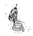
図2は本発明の実施例に係る電池パック100の斜視図である。この電池パック100は、3.6Vのリチウムイオン電池のセルが5本直列接続されたセルユニットが2組収容され、2組のセルユニットの接続方法の変更により、18V出力(低電圧出力)と36V出力(高電圧出力)の双方を切り換えることができる「電圧可変電池パック」である。 FIG. 2 is a perspective view of a battery pack 100 according to an embodiment of the invention. This battery pack 100 accommodates two sets of cell units in which five 3.6V lithium-ion battery cells are connected in series. It is a "voltage variable battery pack" that can switch both 36V output (high voltage output).

電池パック100の筐体は、上下方向に分割可能な下ケース101と上ケース110により形成される。上ケース110は、電動工具本体1の電池パック装着部2c(図3で後述)に取り付けるために2本のレール138a、138bが形成された装着機構が形成される。レール138a、138bは、電池パック100の装着方向と平行な方向に延びるように、且つ、上ケース110の左右側面に突出するように形成される。レール138a、138bは、電動工具本体1の電池パック装着部2cに形成されたレール溝(図示せず)と対応した形状に形成され、レール138a、138bが電気機器本体側のレール溝と嵌合した状態で、ラッチ141の爪となる係止部142にて係止することにより電池パック100が電動工具本体1に固定される。電池パック100を電動工具本体1から取り外すときは、左右両側にあるラッチ141を押すことにより、係止部142が内側に移動して係止状態が解除されるので、その状態で電池パック100を装着方向と反対側に移動させる。 The housing of the battery pack 100 is formed by a lower case 101 and an upper case 110 that can be separated vertically. The upper case 110 is formed with a mounting mechanism having two rails 138a and 138b for mounting on a battery pack mounting portion 2c (described later in FIG. 3) of the power tool body 1. As shown in FIG. Rails 138 a and 138 b are formed to extend in a direction parallel to the mounting direction of battery pack 100 and to protrude from left and right side surfaces of upper case 110 . The rails 138a and 138b are formed in a shape corresponding to rail grooves (not shown) formed in the battery pack mounting portion 2c of the power tool main body 1, and the rails 138a and 138b are fitted to the rail grooves on the electric device main body side. In this state, the battery pack 100 is fixed to the electric power tool main body 1 by engaging with the engaging portion 142 which is the pawl of the latch 141 . When removing the battery pack 100 from the electric power tool main body 1, by pressing the latches 141 on the left and right sides, the locking portions 142 move inward and the locked state is released, so the battery pack 100 can be removed in that state. Move it in the direction opposite to the mounting direction.

上ケース110の下段面111と上段面115は階段状に高さが異なるように形成され、それらの接続部分から後方側に延びる複数のスロット121~128が形成される。スロット121~128は電池パック装着方向に所定の長さを有するように切り欠かれた部分であって、この切り欠かれた部分の内部には、電動工具本体1又は外部の充電装置(図示せず)の機器側端子と嵌合可能な複数の接続端子(接続端子群)が配設される。スロット121~128は、電池パック100の右側のレール138aに近い側のスロット121が充電用正極端子(C+端子)の挿入口となり、スロット122が放電用正極端子(+端子)の挿入口となる。また、左側のレール138bに近い側のスロット127が負極端子(-端子)の挿入口となる。正極端子と負極端子の間には、電池パック100と電動工具本体1や外部の充電装置(図示せず)への信号伝達用の複数の信号端子が配置され、ここでは信号端子用の4つのスロット123~126が電力端子群の間に設けられる。スロット123は予備の端子挿入口であり、本実施例では端子は設けられない。スロット124は電池パック100の識別情報となる信号を電動工具本体又は充電装置に出力するためのT端子用の挿入口である。スロット125は外部の充電装置(図示せず)からの制御信号が入力されるためのV端子用の挿入口である。スロット126はセルに接触して設けられた図示しないサーミスタ(感温素子)による電池の温度情報を出力するためのLS端子用の挿入口である。負極端子(-端子)の挿入口となるスロット127の左側には、さらに電池パック100内に含まれる電池保護回路(図示せず)による異常停止信号を出力するLD端子用のスロット128が設けられる。 The lower surface 111 and the upper surface 115 of the upper case 110 are formed to have different heights, and a plurality of slots 121 to 128 are formed extending rearward from their connecting portion. The slots 121 to 128 are notched portions having a predetermined length in the battery pack mounting direction. A plurality of connection terminals (connection terminal group) that can be fitted with the device-side terminals of (1) are arranged. Of the slots 121 to 128, the slot 121 on the side closer to the right rail 138a of the battery pack 100 serves as an insertion port for the charging positive terminal (C+ terminal), and the slot 122 serves as an insertion port for the discharging positive terminal (+ terminal). . Also, the slot 127 on the side closer to the left rail 138b serves as an insertion port for the negative terminal (-terminal). A plurality of signal terminals for transmitting signals to the battery pack 100, the power tool main body 1, and an external charging device (not shown) are arranged between the positive terminal and the negative terminal. Slots 123-126 are provided between power terminals. The slot 123 is a spare terminal insertion opening, and no terminal is provided in this embodiment. The slot 124 is an insertion opening for a T-terminal for outputting a signal that serves as identification information of the battery pack 100 to the power tool main body or charging device. A slot 125 is an insertion port for a V terminal for receiving a control signal from an external charging device (not shown). The slot 126 is an insertion port for an LS terminal for outputting battery temperature information from a thermistor (temperature sensing element) (not shown) provided in contact with the cell. A slot 128 for an LD terminal is provided on the left side of the slot 127, which serves as an insertion port for the negative terminal (- terminal), for outputting an abnormal stop signal by a battery protection circuit (not shown) included in the battery pack 100. .

上段面115の後方側には、隆起するように形成された隆起部132が形成される。隆起部132の中央付近に窪み状のストッパ部131が形成される。ストッパ部131は、電池パック100を、電池パック装着部2c(図3にて後述)に装着した際に突き当て面となる。電池パック100が電動工具本体1の所定の位置に装着されると電動工具本体1に配設された複数の端子(機器側端子)と電池パック100に配設された複数の接続端子が接触して導通状態となる。下段面111の前方左側角部には、従来の18V用電池パックを36V用の電動工具本体に装着できないようにするための、識別用の切り欠き部111aが形成される。 A protruding portion 132 is formed on the rear side of the upper step surface 115 so as to protrude. A depressed stopper portion 131 is formed near the center of the raised portion 132 . Stopper portion 131 serves as an abutting surface when battery pack 100 is attached to battery pack attachment portion 2c (described later in FIG. 3). When the battery pack 100 is attached to the power tool main body 1 at a predetermined position, the plurality of terminals (equipment-side terminals) provided on the power tool main body 1 and the plurality of connection terminals provided on the battery pack 100 come into contact with each other. becomes conductive. A notch 111a for identification is formed in the front left corner of the lower surface 111 so that the conventional 18V battery pack cannot be attached to the 36V power tool main body.

図3は本発明に係る電池パック100が装着される電動工具本体1の斜視図である。ここで示す電動工具本体1はインパクトドライバであって、ハウジング2の胴体部分から下方に延びるハンドル部2bが設けられ、ハンドル部2bの下側に電池パック装着部10が形成される。ハンドル部2bにはトリガスイッチ4が設けられる。ハウジング2の前方側には出力軸たるアンビル(図示せず)が設けられ、アンビルの先端には先端工具9を装着するための先端工具保持部8が設けられる。ここでは先端工具9としてプラスのドライバービットが装着されている。電動工具だけに限られずに、電池パックを用いた電気機器全般では、装着される電池パックの形状に対応させた電池パック装着部10が形成され、電池パック装着部10に適合しない電池パックを装着できないように構成する。電池パック装着部10には、左右両側の内壁部分に前後方向に平行に延びるレール溝11a、11bが形成され、それらの間にターミナル部20が設けられる。ターミナル部20は、合成樹脂等の不導体材料の一体成形により製造され、そこに金属製の複数の端子、例えば正極入力端子22、負極入力端子27、LD端子(異常信号端子)28が鋳込まれる。ターミナル部20は、装着方向(前後方向)の突き当て面となる垂直面20aと、水平面20bが形成され、水平面20bは電池パック100の装着時に、上段面115(図2参照)と隣接、対向する面となる。水平面20bの前方側には、電池パック100の隆起部132(図2参照)と当接する湾曲部12が形成され、湾曲部12の左右中央付近には突起部14が形成される。突起部14は左右方向に2分割で形成される電動工具本体1のハウジングのネジ止め用のボスを兼ねると共に、電池パック100の装着方向への相対移動を制限するストッパの役目も果たす。 FIG. 3 is a perspective view of the power tool main body 1 to which the battery pack 100 according to the present invention is attached. The power tool main body 1 shown here is an impact driver, and is provided with a handle portion 2b extending downward from the body portion of the housing 2, and a battery pack mounting portion 10 is formed below the handle portion 2b. A trigger switch 4 is provided on the handle portion 2b. An anvil (not shown) serving as an output shaft is provided on the front side of the housing 2, and a tip tool holder 8 for attaching a tip tool 9 is provided at the tip of the anvil. Here, a Phillips screwdriver bit is attached as the tip tool 9 . Not only electric tools but also electric devices using battery packs in general have a battery pack mounting portion 10 corresponding to the shape of the battery pack to be mounted, and a battery pack that does not conform to the battery pack mounting portion 10 is mounted. configure it so that it cannot Rail grooves 11a and 11b extending in parallel in the front-rear direction are formed in the inner wall portions on both left and right sides of battery pack mounting portion 10, and terminal portion 20 is provided between them. The terminal portion 20 is manufactured by integrally molding a non-conductive material such as synthetic resin, and a plurality of metal terminals such as a positive input terminal 22, a negative input terminal 27, and an LD terminal (abnormal signal terminal) 28 are cast into it. be The terminal portion 20 has a vertical surface 20a that serves as an abutting surface in the mounting direction (front-rear direction) and a horizontal surface 20b. It becomes the side to do. A curved portion 12 is formed on the front side of the horizontal surface 20b to abut on the raised portion 132 (see FIG. 2) of the battery pack 100, and a projection portion 14 is formed near the left-right center of the curved portion 12. As shown in FIG. The projecting portion 14 doubles as a boss for screwing the housing of the power tool main body 1, which is divided into two parts in the left-right direction, and also serves as a stopper that restricts the relative movement of the battery pack 100 in the mounting direction.

図4は図3の電池パック100の展開斜視図である。電池パック100の筐体は、上下方向に分離可能な上ケース110と下ケース101によって形成され、下ケース101の内部空間には、10本の電池セルが収容される。複数の電池セル(図示せず)は、5本ずつ2段にスタックさせた状態で、合成樹脂等の不導体で構成されたセパレータ245にて固定される。セパレータ245は電池セルの両端部となる左右両側だけが開口するようにして複数の電池セルを保持する。 4 is an exploded perspective view of the battery pack 100 of FIG. 3. FIG. The housing of the battery pack 100 is formed by a vertically separable upper case 110 and a lower case 101, and the inner space of the lower case 101 accommodates ten battery cells. A plurality of battery cells (not shown) are stacked in two tiers of five each and fixed by separators 245 made of a non-conductor such as synthetic resin. The separators 245 hold a plurality of battery cells so that only the left and right sides, which are both ends of the battery cells, are open.

セパレータ245の上側には、リチウムイオン電池セルを覆うように回路基板150が固定される。回路基板150は複数の接続端子(161、162、164~168、171、172、177)を半田付けによって固定すると共に、これら接続端子と図示しない回路パターンとの電気的な接続を行う。回路基板150にはさらに、電池保護ICやPTCサーミスタ、抵抗、コンデンサ、ヒューズ、発光ダイオード等の様々な電子素子(ここでは図示していない)を搭載する。さらに、点線152で占める領域には、無線通信装置を形成する通信モジュールとアンテナ(ともに後述)が搭載される。回路基板150の材質は、素材に対して絶縁性のある樹脂を含浸した基板上に、銅箔など導電体によってパターン配線を印刷したプリント基板と呼ばれるものであり、単層基板、両面基板、多層基板を用いることができる。本実施例では、両面基板を用いて回路基板150の上面(表面であって図4から見える上側の面)と下面(裏面)に配線パターンが形成される。回路基板150の前後方向の中央よりもやや前側には、接続端子群160が設けられ、そこに複数の接続端子(161、162、164~168、171、172、177)が横方向に並べて固定される。 A circuit board 150 is fixed on the upper side of the separator 245 so as to cover the lithium ion battery cells. The circuit board 150 fixes a plurality of connection terminals (161, 162, 164 to 168, 171, 172, 177) by soldering, and electrically connects these connection terminals to a circuit pattern (not shown). Various electronic elements (not shown here) such as a battery protection IC, a PTC thermistor, a resistor, a capacitor, a fuse, and a light-emitting diode are also mounted on the circuit board 150 . Furthermore, in the area occupied by the dotted line 152, a communication module and an antenna (both described later) forming a wireless communication device are mounted. The material of the circuit board 150 is called a printed board, in which pattern wiring is printed with a conductive material such as copper foil on a board impregnated with an insulating resin. A substrate can be used. In this embodiment, a double-sided board is used to form wiring patterns on the upper surface (the upper surface seen from FIG. 4) and the lower surface (rear surface) of the circuit board 150 . A connection terminal group 160 is provided slightly in front of the center of the circuit board 150 in the front-rear direction, and a plurality of connection terminals (161, 162, 164 to 168, 171, 172, 177) are horizontally arranged and fixed there. be done.

正極端子(161、162、171、172)と負極端子(167、177)は、左右方向に大きく離れた箇所に配置され、それらの間には3つの信号端子(T端子164、V端子165、LS端子166)が設けられる。本実施例では電力端子用の部品として、水平方向に延びる腕部が上側の左右に1組、下側の左右に1組の合計2組設けられたものを用いる。負極端子対(167、177)の左側にはLD端子168が設けられる。すべての信号端子(164~166、168)は、回路基板150の形成された複数の取付孔151a、151bにそれぞれの脚部を表面から裏面にまで貫通させて、裏面側で半田付けにより固定される。以上のように、回路基板150上に図示しない電子素子が搭載され、複数の接続端子が半田付けにより固定されたあとに、回路基板150の表面に防水塵のために樹脂(図示せず)を塗布する。 The positive terminals (161, 162, 171, 172) and the negative terminals (167, 177) are arranged at locations far apart in the horizontal direction, and three signal terminals (T terminal 164, V terminal 165, LS terminal 166) is provided. In this embodiment, two sets of horizontally extending arms, one set on the left and right sides on the upper side and one set on the left and right sides on the lower side, are used as the parts for the power terminals. An LD terminal 168 is provided on the left side of the negative terminal pair (167, 177). All the signal terminals (164 to 166, 168) are fixed by soldering on the back side, with their leg portions penetrating from the front surface to the back surface through a plurality of mounting holes 151a, 151b formed in the circuit board 150. be. As described above, after the electronic elements (not shown) are mounted on the circuit board 150 and the plurality of connection terminals are fixed by soldering, a resin (not shown) is applied to the surface of the circuit board 150 to prevent dust. apply.

下ケース101は、上面が開口された略直方体の形状である。前面壁のほぼ中央には、スリット104が設けられる。上ケース110のスリット134は、充電装置にて充電を行う際に電池パック100の内部空間に充電装置側から送出される冷却風を流入させるための流入口として用いられ、下ケース101のスリット104は冷却風の排出口として用いられる。 The lower case 101 has a substantially rectangular parallelepiped shape with an open upper surface. A slit 104 is provided approximately in the center of the front wall. The slit 134 of the upper case 110 is used as an inlet for introducing cooling air sent from the charging device into the internal space of the battery pack 100 when the battery pack 100 is charged by the charging device. is used as a cooling air outlet.

電池セル側からの出力の回路基板150との接続は、上方向に板状に延びる接続用の引出しタブ261a、266a、271a、276aを介して行われる。また直列接続された電池セルの中間接続点からのリード線の端部294b、296b~299bが上方向に延びるように配置され、回路基板上に半田付けされる。さらに、直列接続された電池セルの中間接続点からの中間引出しタブ262a、263aが回路基板150に接続されるべく、上方向に延びるように配置される。セパレータ245の上側には、回路基板150を固定する為のネジボス247a、247bが形成される。 The output from the battery cell side is connected to the circuit board 150 via connection drawer tabs 261a, 266a, 271a, and 276a extending upward in a plate shape. Lead wire ends 294b, 296b to 299b from intermediate connection points of the battery cells connected in series are arranged to extend upward and are soldered onto the circuit board. Furthermore, intermediate pull-out tabs 262 a and 263 a from intermediate connection points of the battery cells connected in series are arranged to extend upward so as to be connected to the circuit board 150 . Screw bosses 247 a and 247 b for fixing the circuit board 150 are formed on the upper side of the separator 245 .

次に図5を用いて、2組の電力端子の形状を説明する。図5は電池パック100の回路基板150の部分図であり、回路基板150に固定された正極端子対(上側正極端子162と下側正極端子172)と、負極端子対(上側負極端子167と下側負極端子177)だけを図示したものである。図5(A)は本実施例の電池パック100の正極端子(162と172)、負極端子(167と177)の形状を示す部分斜視図と高電圧出力時の接続回路を示す図である。図5(B)は高電圧用電気機器のターミナル部50と、電池パック100側の端子との接続状況を示すための部分斜視図である。図5(A)に示すように、電池パック100のスロット122(図2参照)には、上側正極端子162と下側正極端子172が並んで配置される。上側正極端子162と下側正極端子172は金属板のプレス加工によって形成され、脚部を回路基板150に半田付け等により強固に固定したものである。上側正極端子162と下側正極端子172は距離を隔てて配置され、電気的に非導通状態にある。同様にしてスロット127(図2参照)には、上側負極端子167と下側負極端子177が並んで配置される。上側正極端子162と上側負極端子167は同じ金属部品であり、下側正極端子172と下側負極端子177は同じ金属部品である。 Next, the shapes of the two sets of power terminals will be described with reference to FIG. FIG. 5 is a partial view of the circuit board 150 of the battery pack 100. A positive terminal pair (upper positive terminal 162 and lower positive terminal 172) and a negative terminal pair (upper negative terminal 167 and lower positive terminal 167) fixed to the circuit board 150 are shown in FIG. Only the side negative terminal 177) is illustrated. FIG. 5A is a partial perspective view showing the shapes of the positive terminals (162 and 172) and the negative terminals (167 and 177) of the battery pack 100 of this embodiment, and a diagram showing a connection circuit during high voltage output. FIG. 5B is a partial perspective view showing the state of connection between the terminal portion 50 of the high-voltage electrical equipment and the terminals on the battery pack 100 side. As shown in FIG. 5A, in slot 122 (see FIG. 2) of battery pack 100, upper positive terminal 162 and lower positive terminal 172 are arranged side by side. The upper positive electrode terminal 162 and the lower positive electrode terminal 172 are formed by pressing a metal plate, and their legs are firmly fixed to the circuit board 150 by soldering or the like. The upper positive terminal 162 and the lower positive terminal 172 are spaced apart and electrically non-conductive. Similarly, an upper negative terminal 167 and a lower negative terminal 177 are arranged side by side in the slot 127 (see FIG. 2). The upper positive terminal 162 and the upper negative terminal 167 are the same metal parts, and the lower positive terminal 172 and the lower negative terminal 177 are the same metal parts.

電池パック100の内部には、5本のリチウムイオン電池セルが直列に接続された上側セルユニット(第一セルユニット)146と下側セルユニット(第二セルユニット)147が収容され、上側セルユニット146の正極が第一正極端子に相当する上側正極端子162に接続され、上側セルユニット146の負極が第一負極端子に相当する下側負極端子177に接続される。同様にして、下側セルユニット147の正極が第二正極端子に相当する下側正極端子172に接続され、下側セルユニット147の負極が第二負極端子に相当する上側負極端子167に接続される。このような電池パック100の形態において、電動工具本体1側の正極用入力端子を上側正極端子162に接続し、負極用入力端子を上側負極端子167に接続するとともに、点線59で示すように下側正極端子172と下側負極端子177を電気的に接続すれば、上側セルユニット146と下側セルユニット147の直列接続の出力、即ち定格36Vが電池パック100から電動工具本体1の負荷装置70に出力されることになる。 Inside the battery pack 100, an upper cell unit (first cell unit) 146 and a lower cell unit (second cell unit) 147 in which five lithium ion battery cells are connected in series are housed. The positive terminal of 146 is connected to the upper positive terminal 162 corresponding to the first positive terminal, and the negative terminal of the upper cell unit 146 is connected to the lower negative terminal 177 corresponding to the first negative terminal. Similarly, the positive electrode of the lower cell unit 147 is connected to the lower positive terminal 172 corresponding to the second positive terminal, and the negative electrode of the lower cell unit 147 is connected to the upper negative terminal 167 corresponding to the second negative terminal. be. In such a form of the battery pack 100 , the positive input terminal of the power tool main body 1 is connected to the upper positive terminal 162 , the negative input terminal is connected to the upper negative terminal 167 , and the lower terminal is connected as indicated by the dotted line 59 . If the side positive terminal 172 and the lower side negative terminal 177 are electrically connected, the output of the series connection of the upper cell unit 146 and the lower cell unit 147, that is, the rated voltage of 36 V is transferred from the battery pack 100 to the load device 70 of the power tool body 1. will be output to

出力用の正極端子は、電気的に独立した上側正極端子162と下側正極端子172が、回路基板150の取り付け位置で見て前後方向に並ぶように配置される。これらは互いに近接して配置される複数の端子(162、172)であって、電圧の切替え用に使用される切替端子群として機能する。上側正極端子162と下側正極端子172は、それぞれが前方側に延在する腕部組(腕部162aと162b、腕部172aと172b)を有する。ここでは腕部162a、162bと腕部172a、172bが上下方向に離れた位置であって、その嵌合部の前後方向位置がほぼ同一となるような形状とされる。これら正極端子対(162、172)は、単一のスロット122内に配置される。負極端子対も、正極端子対の形状と同じであって、上側負極端子167と下側負極端子177により構成され、これら負極端子対(167、177)が単一のスロット127の内部に配置される。これらは互いに近接して配置される複数の端子(167、177)であって、電圧の切替え用に使用される切替端子群として機能する。スロット127の内部では、上側に上側負極端子167の腕部組が配置され、上側負極端子167の腕部組の下側に下側負極端子177の腕部組が配置される。尚、図5では図示していないが、放電用の正極端子対(上側正極端子162と下側正極端子172)の右側には、充電用の正極端子対(上側正極端子161と下側正極端子171:図4参照)が配置される。充電用の正極端子対(161、171)の形状は、上側正極端子162と下側正極端子172と同じである。 The output positive terminals are arranged such that the electrically independent upper positive terminal 162 and lower positive terminal 172 are aligned in the front-rear direction when viewed from the mounting position of the circuit board 150 . These are a plurality of terminals (162, 172) placed close to each other, functioning as a group of switching terminals used for switching voltages. The upper positive terminal 162 and the lower positive terminal 172 each have an arm assembly (arms 162a and 162b, arms 172a and 172b) extending forward. Here, the arms 162a, 162b and the arms 172a, 172b are separated in the vertical direction, and the fitting portions are shaped so that the longitudinal positions thereof are substantially the same. These positive terminal pairs ( 162 , 172 ) are located within a single slot 122 . The negative terminal pair also has the same shape as the positive terminal pair, and is composed of an upper negative terminal 167 and a lower negative terminal 177 , which negative terminal pairs ( 167 , 177 ) are located inside a single slot 127 . be. These are a plurality of terminals (167, 177) arranged close to each other and function as a group of switching terminals used for switching voltages. Inside the slot 127 , the arm group of the upper negative terminal 167 is arranged on the upper side, and the arm group of the lower negative terminal 177 is arranged on the lower side of the arm group of the upper negative terminal 167 . Although not shown in FIG. 5, a pair of positive terminals for charging (upper positive terminal 161 and lower positive terminal 172) is provided on the right side of the positive terminal pair for discharging (upper positive terminal 162 and lower positive terminal 172). 171: see FIG. 4) are arranged. The shape of the positive terminal pair (161, 171) for charging is the same as that of the upper positive terminal 162 and the lower positive terminal 172. As shown in FIG.

図5(B)は定格36Vの電動工具本体1のターミナル部50と、電池パック100側の接続端子(162、167、172,177)との接続関係を示す図である。ターミナル部50は、電動工具本体1の電池パック装着部2cに設けられる。ターミナル部50には、電池パック100のスロット121~128(図2参照)に対応する機器側端子(52、59a、54~56、57、59b、58)が設けられ、合成樹脂製の基台51に鋳込まれるようにして固定される。基台51の上側の接続端子部と、下側の板状の端子部であって同じ参照符号の部分は電気的に導通されている金属板により構成される。ここではスロット123(図2参照)に対応する位置には機器側端子は設けられない。電力用の入力端子として、受電用の正極入力端子52と、負極入力端子57が小さいサイズで、短絡用端子59a、59bの上側に設けられる。正極入力端子52と短絡用端子59aは導通していない。また、負極入力端子57と短絡用端子59bは導通していない。 FIG. 5B is a view showing the connection relationship between the terminal portion 50 of the power tool main body 1 rated at 36V and the connection terminals (162, 167, 172, 177) on the battery pack 100 side. The terminal portion 50 is provided on the battery pack mounting portion 2c of the power tool main body 1. As shown in FIG. The terminal portion 50 is provided with device-side terminals (52, 59a, 54-56, 57, 59b, 58) corresponding to the slots 121-128 (see FIG. 2) of the battery pack 100, and a synthetic resin base. It is fixed by being cast into 51 . The connection terminal portion on the upper side of the base 51 and the plate-shaped terminal portion on the lower side having the same reference numerals are formed of electrically conductive metal plates. Here, no device-side terminals are provided at positions corresponding to the slots 123 (see FIG. 2). As input terminals for electric power, a positive input terminal 52 and a negative input terminal 57 for power reception are small in size and provided above the short-circuiting terminals 59a and 59b. The positive input terminal 52 and the short-circuiting terminal 59a are not electrically connected. Also, the negative input terminal 57 and the short-circuiting terminal 59b are not electrically connected.

電池パック100の装着時において、正極入力端子52は上側正極端子162だけに嵌合し、負極入力端子57は上側負極端子167だけに嵌合する。また、電動工具本体1のターミナル部50には、下側正極端子172と下側負極端子177を短絡させる小さい端子59a、59bが設けられる。小さい端子59a、59bは短絡回路59の両側端部であり、基台51の内部で接続されている。 When battery pack 100 is attached, positive input terminal 52 fits only upper positive terminal 162 , and negative input terminal 57 fits only upper negative terminal 167 . The terminal portion 50 of the power tool body 1 is provided with small terminals 59 a and 59 b for short-circuiting the lower positive terminal 172 and the lower negative terminal 177 . Small terminals 59 a and 59 b are opposite ends of short circuit 59 and are connected inside base 51 .

正極入力端子52は、上側正極端子162と嵌合する部分であって平板状に形成された端子部と、電動工具本体1側の回路基板側との結線を行うものであって基台51の上方に突出する端子部により構成される。正極入力端子52は合成樹脂製の基台51に鋳込まれる。負極入力端子57も正極入力端子52と同様であって、端子の高さが、他の端子部(54~56、58)に比べて半分よりやや小さい程度の大きさとされる。他の端子部(54~56、58)は信号伝達用の端子である。ターミナル部50の合成樹脂製の基台51の前側と後側には、ハウジングによって挟持されるための凹部51aと51bが設けられる。 The positive input terminal 52 is a portion to be fitted with the upper positive terminal 162 , and connects a terminal portion formed in a flat plate shape to the circuit board side of the power tool main body 1 side. It is composed of a terminal portion protruding upward. The positive input terminal 52 is cast into the base 51 made of synthetic resin. The negative input terminal 57 is similar to the positive input terminal 52, and the height of the terminal is slightly less than half the height of the other terminal portions (54 to 56, 58). Other terminal portions (54 to 56, 58) are terminals for signal transmission. Recesses 51a and 51b are provided on the front and rear sides of a synthetic resin base 51 of the terminal portion 50 so as to be sandwiched by the housing.

図5(B)において、電池パック100を装着する際には、電池パック100を電動工具本体1に対して差し込み方向に沿って相対移動させると、正極入力端子52と短絡用端子59bが同一のスロット122(図2参照)を通って内部まで挿入され、上側正極端子162と下側正極端子172にそれぞれ嵌合される。このとき、正極入力端子52が上側正極端子162の嵌合部間を押し広げるようにして上側正極端子162の腕部162aと162bの間に圧入され、短絡用端子59bが下側正極端子172の腕部172aと172bの間を押し広げるようにして圧入される。同様にして、負極入力端子57と短絡用端子59bが同一のスロット127(図2参照)を通って内部まで挿入され、それぞれ上側負極端子167と下側負極端子177に嵌合される。この際、負極入力端子57が嵌合部間を押し広げるようにして上側負極端子167の腕部167aと167bの間に圧入される。さらに、短絡用端子59bが下側負極端子177の腕部177aと177bの間を押し広げるようにして圧入される。このように図5(B)の接続形態の実現によって、上側セルユニット146と下側セルユニット147の直列接続の出力、即ち定格36Vが電池パック100から出力されることになる。 In FIG. 5B, when the battery pack 100 is attached, when the battery pack 100 is moved relative to the power tool main body 1 along the insertion direction, the positive input terminal 52 and the short-circuiting terminal 59b are aligned. It is inserted into the inside through the slot 122 (see FIG. 2) and fitted to the upper positive terminal 162 and the lower positive terminal 172, respectively. At this time, the positive input terminal 52 is press-fitted between the arm portions 162 a and 162 b of the upper positive terminal 162 so as to expand the fitting portion of the upper positive terminal 162 , and the short-circuiting terminal 59 b is connected to the lower positive terminal 172 . It is press-fitted so as to expand between the arms 172a and 172b. Similarly, the negative input terminal 57 and the short-circuiting terminal 59b are inserted through the same slot 127 (see FIG. 2) and fitted to the upper negative terminal 167 and the lower negative terminal 177, respectively. At this time, the negative input terminal 57 is press-fitted between the arms 167a and 167b of the upper negative terminal 167 so as to widen the space between the fitting portions. Further, the short-circuiting terminal 59b is press-fitted so as to widen the space between the arms 177a and 177b of the lower negative terminal 177. As shown in FIG. By realizing the connection form of FIG. 5B in this way, the output of the series connection of the upper cell unit 146 and the lower cell unit 147, that is, the rated voltage of 36 V is output from the battery pack 100. FIG.

図6(A)及び(B)は、18V用の電動工具本体1(図3参照)に本実施例の電池パック100を装着した際の接続状態を示す図である。電池パック100が電動工具本体1に取り付けられるときは、正極入力端子82の端子部は、上側正極端子162と下側正極端子172の開口端部の双方を押し広げるように嵌合圧入されて、正極入力端子82の端子部の上側一部の領域が上側正極端子162と接触し、下側一部の領域が下側正極端子172と接触する。このように正極入力端子82の端子部を上側正極端子162の腕部162a、162bと下側正極端子172の腕部172a、172bに同時に嵌合させることによって、2つの正極端子(162と172)が短絡状態となる。同様にして負極入力端子87の端子部は、上側負極端子167と下側負極端子177の開口端部の双方を押し広げるように嵌合圧入されて、負極入力端子87の端子部の上側一部の領域が上側負極端子167と接触し、下側一部の領域が下側負極端子177と接触する。このように負極入力端子87の端子部を上側負極端子167の腕部167a、167bと下側負極端子177の腕部177a、177bに同時に嵌合させることによって、2つの負極端子(167と177)が短絡状態となり、電動工具本体1には上側セルユニット146と下側セルユニット147の並列接続の出力、即ち定格18Vが出力される。 6A and 6B are diagrams showing the connection state when the battery pack 100 of this embodiment is attached to the 18V power tool body 1 (see FIG. 3). When the battery pack 100 is attached to the power tool main body 1, the terminal portion of the positive input terminal 82 is fitted and press-fitted so as to expand both the open end portions of the upper positive terminal 162 and the lower positive terminal 172. An upper portion of the terminal portion of the positive input terminal 82 contacts the upper positive terminal 162 , and a lower portion of the terminal portion contacts the lower positive terminal 172 . By simultaneously fitting the terminal portion of the positive input terminal 82 to the arm portions 162a and 162b of the upper positive terminal 162 and the arm portions 172a and 172b of the lower positive terminal 172, two positive terminals (162 and 172) are connected. is short-circuited. Similarly, the terminal portion of the negative input terminal 87 is fitted and press-fitted so as to expand both the open end portions of the upper negative terminal 167 and the lower negative electrode terminal 177, and the upper portion of the terminal portion of the negative input terminal 87 is pressed. , contacts the upper negative terminal 167 , and a part of the lower region contacts the lower negative terminal 177 . By simultaneously fitting the terminal portion of the negative input terminal 87 to the arm portions 167a and 167b of the upper negative terminal 167 and the arm portions 177a and 177b of the lower negative terminal 177, the two negative terminals (167 and 177) are connected. is short-circuited, and the output of the parallel connection of the upper cell unit 146 and the lower cell unit 147, that is, the rated voltage of 18 V is output to the power tool main body 1 .

以上のように本実施例の電池パック100は、18V用の電動工具本体1(図3参照)か36V用の電動工具本体(図示せず)のいずれかに装着することにより、電池パック100の出力が自動的に切り替わる。この電圧切り替えは電池パック100側にて行うのではなくて、電動工具本体1側のターミナル部の形状によって自動的に行われるので、電圧設定ミスが生ずる虞が全くない。また、電池パック100側には、機械的なスイッチのような専用の電圧切替機構を設ける必要が無いので、構造が単純で故障の虞が低く、長寿命の電池パックを実現できる。 As described above, the battery pack 100 of this embodiment can be installed in either the 18V power tool main body 1 (see FIG. 3) or the 36V power tool main body (not shown). The output switches automatically. This voltage switching is not performed on the battery pack 100 side, but is performed automatically by the shape of the terminal portion on the power tool main body 1 side, so there is absolutely no risk of voltage setting errors. Moreover, since there is no need to provide a dedicated voltage switching mechanism such as a mechanical switch on the battery pack 100 side, a battery pack with a simple structure, low risk of failure, and long life can be realized.

電池パック100を外部充電装置(図示せず)を用いて充電する場合は、従来の18V用電池パックと同じ充電装置にて充電が可能である。電池パック100のスロット121には、上側正極端子162と下側正極端子172と同等の形状の充電用の正極端子が設けられるので、放電用の正極端子(162、172)の代わりに、充電用の正極端子(図示せず)を外部充電装置(図示せず)の正極端子に接続するようにすれば良い。 When the battery pack 100 is charged using an external charging device (not shown), it can be charged with the same charging device as a conventional 18V battery pack. The slot 121 of the battery pack 100 is provided with a positive electrode terminal for charging that has the same shape as the upper positive terminal 162 and the lower positive terminal 172. The positive terminal (not shown) of the external charging device (not shown) may be connected to the positive terminal of the external charging device (not shown).

次に図7の展開斜視図を用いてセパレータ245(図4参照)を用いた電池セルのスタック状況および配線方法を説明する。セパレータ245(図4参照)は10本の電池セル146a~146e、147a~147eを5本ずつ、上下2段にスタックしたものである。図7では電池セル146a~146e、147a~147eがセパレータ245から引き出された状態を示しているが、組立時にはセパレータ245の円筒状の空間246内に挿入され、セパレータの左右両側に露出した端子間に、接続板262~265、272~275にて相互に接続され、引出し板261、266、271、276が電池セルに接続される。その後に、絶縁のために絶縁シート278a、278bが接続板262~265、272~275や引出し板261、266、271、276の上に貼り付けられる。 Next, the state of stacking the battery cells using the separator 245 (see FIG. 4) and the wiring method will be described with reference to the exploded perspective view of FIG. The separator 245 (see FIG. 4) is made by stacking ten battery cells 146a to 146e and 147a to 147e five by five in two tiers. 7 shows the state in which the battery cells 146a to 146e and 147a to 147e are pulled out from the separator 245. During assembly, the battery cells are inserted into the cylindrical space 246 of the separator 245, and between the terminals exposed on the left and right sides of the separator. 262 to 265 and 272 to 275, and the drawer plates 261, 266, 271 and 276 are connected to the battery cells. After that, insulating sheets 278a, 278b are pasted on the connection plates 262-265, 272-275 and the drawer plates 261, 266, 271, 276 for insulation.

各電池セルの軸線はそれぞれ平行になるように積み重ねられ、隣接するセルの向きを交互に逆になるように配置して、隣接する電池セルの正極端子と負極端子を金属製の接続板262~265、272~275を用いて接続される。電池セルの両側端子と接続板262~265、272~275は、複数箇所のスポット溶接によって固定される。ここでは上段に設置された5本の直列接続された電池セルが上側セルユニット146(図9にて詳述)を形成し、下側に設置された5本の直列接続された電池セルが下側セルユニット147(図9にて詳述)を形成する。 The axes of the respective battery cells are stacked in parallel, the directions of adjacent cells are alternately reversed, and the positive and negative terminals of adjacent battery cells are connected to metal connection plates 262 to 262 . 265, 272-275. The terminals on both sides of the battery cells and the connection plates 262 to 265 and 272 to 275 are fixed by spot welding at a plurality of locations. Here, five series-connected battery cells installed on the upper side form an upper cell unit 146 (detailed in FIG. 9), and five series-connected battery cells installed on the lower side form a lower cell unit. A side cell unit 147 (detailed in FIG. 9) is formed.

電池セル146a~146e、147a~147eは、18650サイズと呼ばれる直径18mm、長さ65mmの複数回充放電可能なリチウムイオン電池セル(図示せず)が用いられるが、電池セルのサイズや本数は任意である。電池セルの長さ方向の両端には2つの電極が設けられている。2つの電極のうち、一方は正極であり他方は負極である。 The battery cells 146a to 146e and 147a to 147e use 18650 size lithium-ion battery cells (not shown) that can be charged and discharged multiple times and have a diameter of 18 mm and a length of 65 mm, but the size and number of the battery cells are arbitrary. is. Two electrodes are provided at both ends of the battery cell in the length direction. Of the two electrodes, one is the positive electrode and the other is the negative electrode.

上側セルユニット146の正極は、引出しタブ261aが形成された引出し板261を用いて回路基板150に接続され、上側セルユニット146の負極は、引出しタブ266aが形成された引出し板266を用いて回路基板150に接続される。同様にして下側セルユニット147の正極は、引出しタブ271aが形成された引出し板271を用いて回路基板150に接続され、下側セルユニット147の負極は、引出しタブ276aが形成された引出し板276を用いて回路基板150に接続される。セパレータ245の上面には、金属の薄板を折り曲げた形状の引出し板261、266、271、276のタブを保持するためのタブホルダ250~252、255~257が形成される。タブホルダ250~252、255~257は、L字状に折り曲げられた引出しタブ261a、262a、263a、266a、271a、276aを保持するために形成されるタブ保持部であり、セパレータ245の成形時に座面、背面、両側側面を有する凹部として一体成形され、この凹部に引出しタブ261a、262a、263a、266a、271a、276aがそれぞれ嵌め込まれる。セパレータ245の上部には回路基板150をネジ止めするための2つのネジボス247a、247bが形成される。引出し板261、271と接続板263、265、273、275の右側は絶縁シート278aにて覆われ、引出し板266、276と接続板262、264、272、274の左側は絶縁シート278bにて覆われる。絶縁シート278aは電気を通さない材質であって、その内側部分はシール材が塗布されている。 The positive electrode of the upper cell unit 146 is connected to the circuit board 150 using a drawer plate 261 having a drawer tab 261a formed thereon, and the negative electrode of the upper cell unit 146 is connected to the circuit using a drawer plate 266 having a drawer tab 266a formed thereon. It is connected to the substrate 150 . Similarly, the positive electrode of the lower cell unit 147 is connected to the circuit board 150 using a drawer plate 271 having a drawer tab 271a formed thereon, and the negative electrode of the lower cell unit 147 is connected to the drawer plate 276a having a drawer tab 276a formed thereon. 276 to the circuit board 150 . Tab holders 250 to 252 and 255 to 257 for holding the tabs of the drawer plates 261, 266, 271 and 276 are formed on the upper surface of the separator 245. The tab holders 250 to 252 and 255 to 257 are formed by bending thin metal plates. The tab holders 250 to 252 and 255 to 257 are tab holders formed to hold the L-shaped drawer tabs 261a, 262a, 263a, 266a, 271a and 276a. It is integrally molded as a recess having a face, a back and side surfaces, into which the drawer tabs 261a, 262a, 263a, 266a, 271a and 276a are fitted respectively. Two screw bosses 247 a and 247 b for screwing the circuit board 150 are formed on the separator 245 . The right side of the drawer plates 261, 271 and connection plates 263, 265, 273, 275 is covered with an insulating sheet 278a, and the left side of the drawer plates 266, 276 and the connection plates 262, 264, 272, 274 is covered with an insulating sheet 278b. will be The insulating sheet 278a is made of a material that does not conduct electricity, and the inner portion thereof is coated with a sealing material.

図8は電池パック100が装着される電動工具本体(高電圧用電気機器)1の回路図であり、電動工具本体1内に短絡回路(短絡経路)59を組み込んだ構成である。右側が電池パック100であり、ここでは説明を容易にするため必要な構成だけを抜き出して図示している。定格36Vの電動工具本体1に、電池パック100から36Vの電圧を取り出すのは、電動工具本体1側のターミナル部50に、太線で示す短絡回路59を設ける。短絡回路59は金属板でできた短絡子で構成でき、図5で示したように正極入力端子52や負極入力端子57等の他の機器側端子と共に、合成樹脂製の基台51にU字状に折り曲げた金属板を鋳込むことで構成できる。U字状に折り曲げた金属板の一方側の端部が短絡用端子59aとなり、他方側の端部が短絡用端子59bとなる。このような形状のターミナル部50に電池パック100を装着するだけで、正極入力端子52と負極入力端子57に定格36Vの直流電力が供給される。電動工具本体1には、モータ3の回転制御を行うためのマイコン60が含まれる。マイコン60の駆動用の電圧(5V又は3.3V)は、短絡用端子59aと負極入力端子57の両端電圧を入力とする電源装置61により供給される。このように電動工具本体1に短絡回路59を有するターミナル部50を設けることによって、2つの正極端子(162、172)と2つの負極端子(167、177)を有する本実施例の電池パック100を装着するだけで、上側セルユニット146と下側セルユニット147の直列接続回路を確立することができる。 FIG. 8 is a circuit diagram of the power tool main body (high-voltage electric device) 1 to which the battery pack 100 is attached, and has a configuration in which a short circuit (short circuit path) 59 is incorporated in the power tool main body 1 . The right side is the battery pack 100, and only the necessary configuration is extracted and illustrated here for the sake of easy explanation. The voltage of 36 V is extracted from the battery pack 100 to the power tool main body 1 rated at 36 V by providing a short circuit 59 indicated by a thick line in the terminal portion 50 on the power tool main body 1 side. The short circuit 59 can be composed of a short circuit made of a metal plate, and as shown in FIG. It can be constructed by casting a metal plate bent into a shape. One end of the U-shaped bent metal plate serves as a short-circuit terminal 59a, and the other end serves as a short-circuit terminal 59b. By simply attaching the battery pack 100 to the terminal portion 50 having such a shape, the positive input terminal 52 and the negative input terminal 57 are supplied with a DC power rated at 36V. The power tool main body 1 includes a microcomputer 60 for controlling the rotation of the motor 3 . A voltage (5 V or 3.3 V) for driving the microcomputer 60 is supplied by a power supply device 61 that receives the voltage across the short-circuiting terminal 59a and the negative input terminal 57 as input. By providing the terminal portion 50 having the short circuit 59 in the power tool body 1 in this way, the battery pack 100 of this embodiment having two positive terminals (162, 172) and two negative terminals (167, 177) can be obtained. A series connection circuit of the upper cell unit 146 and the lower cell unit 147 can be established only by attaching them.

図9は本実施例の電池パック100の内部回路を示すブロック図である。ここでは上側セルユニット146及び下側セルユニット147に対する、マイコン154と保護IC180、190の接続状況を説明するための基本的な構成部分だけを図示しており、その他の関連する回路、特に、本体機器側の信号端子とのやりとりを行うための回路等の図示を省略している。電池パック100は、図4にて示したように上側正極端子(上+)162と、下側正極端子(下+)172と、上側負極端子(上-)167と、下側負極端子(下+)177を有して構成される。電池パック100にはこれら以外に、その他の信号端子群(T端子、V端子、LS端子、LD端子)が設けられるが、ここではそれらの図示を省略している。上側正極端子162と下側負極端子177には、上側セルユニット146の出力が接続される。即ち、上側セルユニット146の正極(+出力)が上側正極端子162に接続され、上側セルユニット146の負極(-出力)が下側負極端子177に接続される。同様にして、下側セルユニット147の正極(+出力)が下側正極端子172に接続され、下側セルユニット147の負極(-出力)が上側負極端子167に接続される。 FIG. 9 is a block diagram showing the internal circuitry of the battery pack 100 of this embodiment. Here, only the basic components for explaining the connection status of the microcomputer 154 and the protection ICs 180 and 190 to the upper cell unit 146 and the lower cell unit 147 are illustrated, and other related circuits, particularly the main body, are illustrated. Illustrations of circuits and the like for communicating with signal terminals on the device side are omitted. As shown in FIG. 4, the battery pack 100 has an upper positive terminal (upper +) 162, a lower positive terminal (lower +) 172, an upper negative terminal (up-) 167, and a lower negative terminal (lower +) 177. In addition to these, the battery pack 100 is provided with other signal terminal groups (T terminal, V terminal, LS terminal, and LD terminal), but illustration thereof is omitted here. The output of the upper cell unit 146 is connected to the upper positive terminal 162 and the lower negative terminal 177 . That is, the positive electrode (+ output) of the upper cell unit 146 is connected to the upper positive electrode terminal 162 and the negative electrode (- output) of the upper cell unit 146 is connected to the lower negative electrode terminal 177 . Similarly, the positive (+ output) of lower cell unit 147 is connected to lower positive terminal 172 and the negative (- output) of lower cell unit 147 is connected to upper negative terminal 167 .

上側セルユニット146と下側セルユニット147にはそれぞれ、電池セルの電圧を監視するための保護IC180、190が接続され、これら保護IC180、190にはマイコン154が接続される。保護IC180は、上側セルユニット146の各電池セルの両端電圧を入力することにより、過充電保護機能、過放電保護機能の他、セルバランス機能、カスケード接続機能、断線検出機能を実行するもので、“リチウムイオン電池用保護IC”として市販されている集積回路である。また、保護IC180は、上側セルユニット146の電池セルの電圧が所定値未満に低下して過放電状態になった場合は、過放電を示す信号(ハイ信号)183をマイコン154に出力し、上側セルユニット146の電池セルの電圧が充電時に所定値以上に到達して過充電状態でなった場合は、過充電を示す信号(ハイ信号)184をマイコン154に出力する。 Protection ICs 180 and 190 for monitoring the voltage of the battery cells are connected to the upper cell unit 146 and the lower cell unit 147, respectively. The protection IC 180 receives the voltage across each battery cell of the upper cell unit 146 to perform overcharge protection, overdischarge protection, cell balancing, cascade connection, and disconnection detection. It is an integrated circuit marketed as a “Protection IC for Lithium Ion Battery”. In addition, when the voltage of the battery cell of the upper cell unit 146 drops below a predetermined value and becomes over-discharged, the protection IC 180 outputs a signal (high signal) 183 indicating over-discharge to the microcomputer 154, When the voltage of the battery cell of the cell unit 146 reaches a predetermined value or more during charging and the battery is overcharged, a signal (high signal) 184 indicating overcharge is output to the microcomputer 154 .

下側セルユニット147には保護IC190が接続される。ここでは、下側セルユニット147の回路中、即ち下側正極端子172と上側負極端子167の間の回路中に、マイコン(Micro Controller Unit)154が接続される。マイコン154には、保護IC180からの出力(過放電信号183、過充電信号184)と、保護IC190からの出力(過放電信号191、過充電信号192)が入力される。マイコン154には、例えばアナログ・フロント・エンド(AFE)と呼ばれる電圧検出回路を含み、電流検出回路193の出力電圧から下側セルユニット147に流れる電流値を測定する。マイコン154の駆動用の電源は、下側セルユニット147に接続される電源回路185によって生成され、電源電圧(VDD1)がマイコン154に供給される。下側セルユニット147のグランド側には電流値を測定するためのシャント抵抗194が設けられる。 A protection IC 190 is connected to the lower cell unit 147 . Here, a microcomputer (Micro Controller Unit) 154 is connected in the circuit of the lower cell unit 147 , that is, in the circuit between the lower positive terminal 172 and the upper negative terminal 167 . The output from the protection IC 180 (overdischarge signal 183 and overcharge signal 184) and the output from the protection IC 190 (overdischarge signal 191 and overcharge signal 192) are input to the microcomputer 154 . The microcomputer 154 includes a voltage detection circuit called an analog front end (AFE), for example, and measures the current value flowing through the lower cell unit 147 from the output voltage of the current detection circuit 193 . A power supply for driving the microcomputer 154 is generated by a power supply circuit 185 connected to the lower cell unit 147 , and a power supply voltage (VDD1) is supplied to the microcomputer 154 . A shunt resistor 194 for measuring the current value is provided on the ground side of the lower cell unit 147 .

マイコン154は、電流値やセル温度の監視を行うと共に、上側セルユニット146と下側セルユニット147の状態を監視して双方の動作状況を統合して制御する。また、電動工具本体1の緊急的な停止が必要となった場合には、図示しないLD端子を介して放電禁止信号を電気機器本体側に送出する。保護IC190は下側セルユニット147内の電池セルの電圧を監視し、電圧が所定の下限値まで低下した状態(過放電状態)を検出した場合に過放電信号191をマイコン154に送出する。マイコン154には、図示しないマイクロプロセッサとともに、タイマー回路や記憶装置が含まれる。マイコン154は監視された電池電圧、温度、充電回数のカウント値を記憶装置に格納する。 The microcomputer 154 monitors the current value and cell temperature, monitors the states of the upper cell unit 146 and the lower cell unit 147, and controls the operating conditions of both in an integrated manner. Further, when it becomes necessary to urgently stop the power tool main body 1, a discharge prohibition signal is sent to the electric device main body through an LD terminal (not shown). The protection IC 190 monitors the voltage of the battery cells in the lower cell unit 147 and sends an over-discharge signal 191 to the microcomputer 154 when the voltage drops to a predetermined lower limit (over-discharge state). The microcomputer 154 includes a microprocessor (not shown), a timer circuit, and a storage device. The microcomputer 154 stores the monitored battery voltage, temperature, and count value of the number of times of charging in a storage device.

マイコン154には無線通信回路155が接続される。無線通信回路155にはアンテナ156が接続される。ここでは市販されている無線通信モジュール153を用いて、それを回路基板150に搭載する。無線通信モジュール153は、無線通信回路155とアンテナ156を共通のベース(図示せず)にまとめて搭載したものである。ここで、無線通信モジュール153又はアンテナ156が本発明における無線通信部に該当する。 A wireless communication circuit 155 is connected to the microcomputer 154 . An antenna 156 is connected to the wireless communication circuit 155 . Here, a commercially available wireless communication module 153 is used and mounted on the circuit board 150 . The wireless communication module 153 has a wireless communication circuit 155 and an antenna 156 mounted together on a common base (not shown). Here, the wireless communication module 153 or the antenna 156 corresponds to the wireless communication section in the present invention.

電池パック100が図示しない外部の充電装置に装着されて、充電が行われている際に、保護IC190は電池セルの電圧が所定の上限値を越えたことを検出した場合に、過充電状態を示す過充電信号192をマイコン154に送出する。マイコン154はその情報を記憶装置に格納するとともに、図示しないLS端子を介して図示しない充電装置に充電停止信号を送出する。 When the battery pack 100 is attached to an external charging device (not shown) and is being charged, the protection IC 190 detects that the voltage of the battery cell has exceeded a predetermined upper limit value. An overcharge signal 192 shown is sent to the microcomputer 154 . The microcomputer 154 stores the information in a storage device and sends a charging stop signal to a charging device (not shown) through an LS terminal (not shown).

電源回路185は、下側セルユニット147の電力によってマイコン154の動作用の電源を生成するものである。下段側にマイコン154用の電源回路185を設け、マイコン154を下側セルユニット147の回路中に設けた。このマイコン154の配置により、出力電圧を定格18Vと36Vの切替式としてもマイコン154を安定して稼働させることができる。マイコン154は、自身にかかる電源電圧(VDD1)の保持と、解除を切り替えることができ、通常動作状態(ノーマルモード)と動作停止状態(いわゆるスリープモード)を有する。 The power supply circuit 185 generates power for operating the microcomputer 154 from the power of the lower cell unit 147 . A power supply circuit 185 for the microcomputer 154 is provided on the lower side, and the microcomputer 154 is provided in the circuit of the lower cell unit 147 . Due to this layout of the microcomputer 154, the microcomputer 154 can be stably operated even if the output voltage is switched between the rated 18V and 36V. The microcomputer 154 can switch between holding and releasing the power supply voltage (VDD1) applied to itself, and has a normal operation state (normal mode) and an operation stop state (so-called sleep mode).

マイコン154には、上側正極端子162に接続される上側電圧検出回路182の出力が入力される。この出力は、電池パック100が電動工具本体1や外部充電装置(図示せず)に装着されていない場合は、上側セルユニット146の電位を示す。一方、低電圧(18V)用の電動工具本体1に装着された場合、上側正極端子162と下側正極端子172が接続されるため、上側セルユニット146と下側セルユニット147の各々の正極が同電位となり、各々の負極が同電位となる。このことからマイコン154は、上側正極端子162の電位と、下側正極端子172の電位を比較することによって、電池パック100が非装着の状態であるか、低電圧機器本体に装着されているか、高電圧機器に装着されているかを判別できる。尚、下側正極端子172の電位検出のためには、下側セルユニット147内の電池セルのうち最上位の電池セル147aの正極電位をマイコン154が取得できるように構成すると良い。図5では図示していないが、電池パック100からの電力供給を止めなければならない状況、例えば、放電時の過大電流、放電時のセル電圧の低下(過放電)、セル温度の異常上昇(過温度)等が生じた際には、マイコン154を介して電動工具本体側にLD信号を伝達することで、電動工具本体1の動作を素早く停止できる。 The output of the upper voltage detection circuit 182 connected to the upper positive terminal 162 is input to the microcomputer 154 . This output indicates the potential of the upper cell unit 146 when the battery pack 100 is not attached to the power tool main body 1 or an external charging device (not shown). On the other hand, when attached to the power tool body 1 for low voltage (18V), the upper positive electrode terminal 162 and the lower positive electrode terminal 172 are connected, so that the positive electrodes of the upper cell unit 146 and the lower cell unit 147 are connected. It becomes the same electric potential, and each negative electrode becomes the same electric potential. Accordingly, the microcomputer 154 compares the potential of the upper positive terminal 162 and the potential of the lower positive terminal 172 to determine whether the battery pack 100 is in the non-attached state or attached to the low-voltage device main body. It can be determined whether it is attached to a high-voltage device. In order to detect the potential of the lower positive electrode terminal 172 , it is preferable to configure the microcomputer 154 to acquire the positive electrode potential of the battery cell 147 a at the highest level among the battery cells in the lower cell unit 147 . Although not shown in FIG. 5, situations in which the power supply from the battery pack 100 must be stopped, such as excessive current during discharge, drop in cell voltage during discharge (overdischarge), and abnormal rise in cell temperature (overdischarge). temperature), the operation of the power tool body 1 can be quickly stopped by transmitting the LD signal to the power tool body side via the microcomputer 154 .

図10は図5に示した部品を組み立てた後のセパレータ245の側面図であり、(A)は右側面であり、(B)は左側面図である。ここでは説明上の容易さから、接続端子群は、放電用の正極端子(162、177)と、負極端子(167、177)の2組だけを図示し、その他の接続端子(161、164~166,168、171)の図示を省略している。また、回路基板150の上の樹脂層は形成される前の状況を示している。上側セルユニット146は上段側に配置された電池セル146a~146eにより構成され、正極側の引出し板261から上方に延びる引出しタブ261aと、負極側の引出し板266から上方に延びる引出しタブ266aにて回路基板150に接続される。回路基板150にはスリット状の貫通孔(図示せず)が開けられ、その貫通孔を下側から上側まで貫通させて、引出しタブ261a、266aの上部が回路基板150の表面から上側に露出する。その部分を半田付けすることにより、回路基板150と引出しタブ261a、266aとの電気的な接続が行われる。同様にして、下側セルユニット147は下段側に配置された電池セル147a~147eにより構成され、両端に設けられた引出し板271、276から上方に延びる接続用の引出しタブ271a、276aにて回路基板150に接続される。回路基板150にはスリット状の貫通孔(図示せず)が開けられ、その貫通孔を下側から上側まで貫通させて、引出しタブ271a、276aの上部が回路基板150の表面から上側に露出する。その部分を半田付けすることにより、回路基板150と引出しタブ271a、276aとの電気的な接続が行われる。 10 is a side view of the separator 245 after assembling the parts shown in FIG. 5, (A) is a right side view and (B) is a left side view. Here, for ease of explanation, only two groups of connection terminals, positive terminals (162, 177) for discharge and negative terminals (167, 177) are shown, and other connection terminals (161, 164 to 166, 168, 171) are omitted. Also, the state before the resin layer on the circuit board 150 is formed is shown. The upper cell unit 146 is composed of battery cells 146a to 146e arranged on the upper side, with a drawer tab 261a extending upward from a drawer plate 261 on the positive electrode side and a drawer tab 266a extending upward from a drawer plate 266 on the negative electrode side. It is connected to the circuit board 150 . A slit-like through hole (not shown) is formed in the circuit board 150, and the through hole penetrates from the bottom to the top, and the upper portions of the pull-out tabs 261a and 266a are exposed upward from the surface of the circuit board 150. . By soldering the portion, electrical connection between the circuit board 150 and the lead-out tabs 261a, 266a is established. Similarly, the lower cell unit 147 is composed of the battery cells 147a to 147e arranged on the lower side, and is connected to the circuit by the connecting drawer tabs 271a and 276a extending upward from the drawer plates 271 and 276 provided at both ends. It is connected to the substrate 150 . A slit-shaped through-hole (not shown) is formed in the circuit board 150, and the through-hole penetrates from the bottom to the top so that the upper portions of the pull-out tabs 271a and 276a are exposed upward from the surface of the circuit board 150. . By soldering the portion, electrical connection between the circuit board 150 and the lead-out tabs 271a and 276a is established.

図10(A)に示す接続板263には上方に延びる中間引出しタブ263aが設けられ、図10(B)に示す接続板262には上方に延びる中間引出しタブ262aが設けられる。中間引出し262a、263aは、上段側に配置される接続板262、263から上側に板状部材を延ばして、回路基板150に沿って内側に折り曲げ、再度上側に折り曲げることによって中間引出しタブ262a、263aを形成した金属の薄板の折曲体である。回路基板150にはスリット状の貫通孔(図示せず)が開けられ、その貫通孔を下側から上側まで貫通させて、中間引出しタブ262a、263aの上部が回路基板150の表面から上側に露出する。中間引出しタブ262a、263aは回路基板150に半田付けすることにより固定される。中間引出しタブ262a、263aの幅(前後方向の距離)は、図10(A)の引出しタブ261aや図10の引出しタブ266aの幅(前後方向長さ)よりも小さく形成される。これは引出しタブ261a、266a、271a、276aは電力の出力用の端子であって高電圧、大電流が流れる端子であるのに対して、中間引出しタブ262a、263aは中間電位の測定用に接続される端子であり、わずかな電流しか流れないためである。上段側に設けられるその他の接続板264と接続板265にも中間引出しタブを形成することも可能である。しかしながら、ここでは配線パターンの形成の関係から、接続端子264a、265aを設けて図示しないリード線にて回路基板150と接続することにした。下段側に設けられる接続板272~275については、引出しタブによる回路基板150との接続が困難であるため、接続端子272a~275aを設けてリード線296~299にて回路基板150と接続するようにした。 A connection plate 263 shown in FIG. 10A is provided with an intermediate drawer tab 263a extending upward, and a connection plate 262 shown in FIG. 10B is provided with an intermediate drawer tab 262a extending upward. Intermediate drawers 262a and 263a are formed by extending plate-shaped members upward from connection plates 262 and 263 arranged on the upper side, bending them inward along circuit board 150, and bending them upward again to form intermediate drawer tabs 262a and 263a. It is a bent body of a thin metal plate that forms a . A slit-shaped through hole (not shown) is formed in the circuit board 150, and the upper part of the intermediate drawer tabs 262a and 263a is exposed upward from the surface of the circuit board 150 by penetrating the through hole from the bottom to the top. do. Intermediate drawer tabs 262a, 263a are fixed to circuit board 150 by soldering. The width (length in the front-rear direction) of the intermediate drawer tabs 262a and 263a is smaller than the width (the length in the front-rear direction) of the drawer tab 261a in FIG. 10A and the drawer tab 266a in FIG. The pull-out tabs 261a, 266a, 271a, and 276a are terminals for outputting electric power and are terminals through which high voltage and large current flow, while the intermediate pull-out tabs 262a and 263a are connected for measuring intermediate potential. This is because it is a terminal that is connected to the terminal and only a small amount of current flows through it. It is also possible to form intermediate pull-out tabs on other connection plates 264 and 265 provided on the upper side. However, here, connection terminals 264a and 265a are provided and connected to the circuit board 150 by lead wires (not shown) because of the formation of the wiring pattern. Since it is difficult to connect the connecting plates 272 to 275 provided on the lower side to the circuit board 150 by means of the lead-out tabs, connection terminals 272a to 275a are provided and connected to the circuit board 150 by lead wires 296 to 299. made it

図11はセパレータ245に回路基板150を固定した状態を示す斜視図であって、左前上方より見た状態を示す。回路基板150にはスリット状の貫通孔159a~159dからタブ261a、266a、271a、276aの上部が回路基板150の表面から上側に露出する。それらのタブの露出部分を半田付けすることにより、回路基板150と引出しタブ261a、266a、271a、276aとの電気的な接続が行われる。以上のようにして上側セルユニット146の電池セル146a~146eは回路基板150に直接接続され、下側セルユニット147の電池セル147a~147eは回路基板150に直接接続される。また、接続板262~264及び接続板272~274の電位を測定するためのリード線296~299(但し図11では297、299は見えない)が接続される。図4に示したリード線の端部294b、296b、297b、298b、299bは回路基板150に半田付けされる。回路基板150に近接している接続板262、263(図12参照)は、L字状に折り曲げられ、垂直板部分が上方に延びる中間引出しタブ262a、263aを用いて回路基板150に直接接続される。 FIG. 11 is a perspective view showing a state in which the circuit board 150 is fixed to the separator 245, viewed from the upper left front. The upper portions of the tabs 261a, 266a, 271a and 276a are exposed upward from the surface of the circuit board 150 through the slit-shaped through holes 159a to 159d. Electrical connections between the circuit board 150 and the lead tabs 261a, 266a, 271a, 276a are made by soldering the exposed portions of those tabs. Battery cells 146 a to 146 e of upper cell unit 146 are directly connected to circuit board 150 as described above, and battery cells 147 a to 147 e of lower cell unit 147 are directly connected to circuit board 150 . Lead wires 296 to 299 (however, 297 and 299 are not visible in FIG. 11) are connected to measure the potentials of the connection plates 262 to 264 and the connection plates 272 to 274, respectively. The ends 294b, 296b, 297b, 298b, 299b of the leads shown in FIG. The connection plates 262, 263 (see FIG. 12) adjacent to the circuit board 150 are bent into an L shape and the vertical plate portions are directly connected to the circuit board 150 using upwardly extending intermediate pull-out tabs 262a, 263a. be.

上側セルユニット146の出力(+出力、-出力)用の引出しタブ261a、266aは正面視又は後面視で略L字形状となるような形状とされ、その長手方向は略長方形の回路基板150の長辺と平行になるように配置される。引出しタブ261a、266aは、引出し板261、266の電池セルの端子に固定された面を上側に延ばして内側に折り曲げ、セパレータの上面を水平方向内側に少し延ばして、適当な箇所で上方向にL字状に折り曲げることにより、折り曲げた鉛直壁部分を引出しタブ261a、266aとした、金属の薄板の折曲体である。しかしながら、下段に配置した電池セルからは、上段に電池セル用の電極が位置するため、同様の引き出し方法は採用できない。そこで、本実施例では下側セルの端子面271b(図13(A)も参照)からの引出し板271を前方側に延ばしてから左側に直角に折り曲げて側面部271cを形成し、側面部271cを上側に延ばす。つまり、引出し板271をセパレータ245の上面視で短辺側となる側面を這わせて上方向に延ばし、セパレータ245の前側側面から後方側に折り曲げて水平面部271dを形成し、水平面部271dを上側に直角にタブ状に延ばして引出しタブ271aを形成した。引出しタブ271aは回路基板150に形成されたスリット状の貫通孔159cを裏面から表面まで貫通させ、半田付けされる。引出しタブ271a、276aの長手方向は略長方形の短辺と平行になるように配置される。このように形成することによって、下段側の電池セルからの引出し板271を、上段側の電池セルの引出し板に干渉することなく配置することができる。 The pull-out tabs 261a and 266a for the output (+output, -output) of the upper cell unit 146 are shaped so as to have a substantially L shape when viewed from the front or rear, and the longitudinal direction of the tabs is the substantially rectangular shape of the circuit board 150. It is arranged parallel to the long side. The pull-out tabs 261a and 266a are formed by extending the surfaces of the pull-out plates 261 and 266 fixed to the battery cell terminals upward and bending them inward, extending the upper surface of the separator slightly inward in the horizontal direction, and then upward at appropriate points. It is a bent body of a thin metal plate that is bent into an L shape so that the bent vertical wall portions are used as pull-out tabs 261a and 266a. However, from the battery cells arranged in the lower stage, since the electrodes for the battery cells are located in the upper stage, the same extraction method cannot be adopted. Therefore, in this embodiment, the drawer plate 271 from the terminal surface 271b (see also FIG. 13A) of the lower cell is extended forward and then bent to the left at a right angle to form the side portion 271c. extend upward. That is, the drawer plate 271 is extended upward along the short side of the separator 245 when viewed from above, and is bent rearward from the front side surface of the separator 245 to form a horizontal surface portion 271d. was extended in a tab shape at right angles to the drawer tab 271a. The lead-out tab 271a is passed through a slit-like through hole 159c formed in the circuit board 150 from the rear surface to the front surface and is soldered. The longitudinal direction of the drawer tabs 271a and 276a is arranged parallel to the short sides of the substantially rectangular shape. By forming in this way, the drawer plate 271 from the lower battery cell can be arranged without interfering with the drawer plate of the upper battery cell.

下段のマイナス端子からの引出し板276も同様の方法で引き出され(後述の図12参照)、引出しタブ276aまで引き出される。このように、セパレータを左右両側側面だけでなく、前側側面及び後側側面を利用して上方向に引き出すことによって、下段に配置された電池セルからの出力を、上段の電池セルの上側部分、即ちセパレータの上面部にまで効率良く引き出すことができる。引出し板271にはさらに、接続経路の幅を大きく絞った部分、即ちヒューズ部271eを形成した。ヒューズ部271eは、引出し板271の右側から切り抜き部271fを形成し、左側から切り抜き部271gを形成して残りの部分の幅(左右方向幅)を十分狭くしたもので、この部分によって引出し板271に電力ヒューズとしての機能を持たせた。同様のヒューズ機能は、上側セルユニット146のプラス端子からの引出し板261(図12参照)の引出しタブ261aの近傍にも同様に設けられる。隣接する電池セルの電極間を接続するための長円状の接続板262、264、273、274は、ステンレス等の金属の薄板にて形成され、電池セルに対してスポット溶接をすることで固定される。 The pull-out plate 276 from the lower negative terminal is also pulled out in a similar manner (see FIG. 12, which will be described later), and is pulled out to the pull-out tab 276a. In this way, by pulling out the separator upward using not only the left and right side surfaces, but also the front and rear side surfaces, the output from the battery cells arranged in the lower stage can be transferred to the upper part of the upper battery cell That is, it can be efficiently pulled out to the upper surface of the separator. The lead-out plate 271 is further formed with a portion where the width of the connection path is greatly reduced, that is, a fuse portion 271e. The fuse portion 271e is formed by forming a cutout portion 271f from the right side of the drawer plate 271 and forming a cutout portion 271g from the left side of the drawer plate 271 so that the width of the remaining portion (horizontal direction width) is sufficiently narrowed. function as a power fuse. A similar fuse function is similarly provided in the vicinity of the pull-out tab 261a of the pull-out plate 261 (see FIG. 12) from the positive terminal of the upper cell unit 146. FIG. The oval connection plates 262, 264, 273, and 274 for connecting the electrodes of adjacent battery cells are formed of thin metal plates such as stainless steel, and are fixed to the battery cells by spot welding. be done.

上側セルユニット146は、プラス出力用として引出しタブ261aが設けられ、マイナス出力用として引出しタブ266aが設けられる。また、下側セルユニット147は、プラス出力用として引出しタブ271aが設けられ、マイナス出力用として引出しタブ276aが設けられる。本実施例では引出しタブ261a、266a、271a、276aの設置位置も工夫した。回路基板150の左右中心線又は正極端子対(162、172)と負極端子対(167、177)の中心線を点線で示す左右中心線A1とする。また、上側正極端子162と下側正極端子172の脚部間の中心位置と、上側負極端子167と下側負極端子177の脚部間の中心位置の2つの中心位置を結んだ線を点線で示す仮想線A2とする。これら左右中心線A1と前後方向の脚部中心線A2を引いた際に、上側正極端子162の脚部がある領域内に上側セルユニット146の正極の引出しタブ261aが存在し、下側正極端子172の脚部がある領域内に下側セルユニット147の正極の引出し板271aが存在するようにした。このように引出しタブ261a、271aを配置することによって引出しタブ261aと上側正極端子162、引出し板271aと下側正極端子172を回路基板150上に配置する配線パターンにて効率良く接続できる。同様にして、上側負極端子167の脚部がある領域内に下側セルユニット147の負極の引出しタブ276aが存在し、下側負極端子177の脚部がある領域内に上側セルユニット146の負極の引出しタブ266aが存在するようにした。このように引出しタブ276a、266aを配置することによって上側負極端子167、下側負極端子177と回路基板150上に配置する配線パターンにて効率良く接続できる。 The upper cell unit 146 is provided with a pullout tab 261a for positive output and a pullout tab 266a for negative output. In addition, the lower cell unit 147 is provided with a pull-out tab 271a for plus output and a pull-out tab 276a for minus output. In this embodiment, the installation positions of the drawer tabs 261a, 266a, 271a, and 276a are also devised. The left-right center line of the circuit board 150 or the center line of the positive terminal pair (162, 172) and the negative terminal pair (167, 177) is defined as a left-right center line A1 indicated by a dotted line. A dotted line is a line connecting two center positions, that is, a center position between the legs of the upper positive terminal 162 and the lower positive terminal 172 and a center position between the legs of the upper negative terminal 167 and the lower negative terminal 177. A virtual line A2 is shown. When the left-right center line A1 and the leg center line A2 in the front-rear direction are drawn, the pull-out tab 261a for the positive electrode of the upper cell unit 146 exists in the region where the leg of the upper positive electrode terminal 162 is located, and the lower positive electrode terminal is located. A lead plate 271a of the positive electrode of the lower cell unit 147 was arranged to exist in the area where the leg portion of the cell unit 172 is located. By arranging the pull-out tabs 261 a and 271 a in this manner, the pull-out tab 261 a and the upper positive terminal 162 and the pull-out plate 271 a and the lower positive terminal 172 can be efficiently connected by the wiring pattern arranged on the circuit board 150 . Similarly, the pull-out tab 276a for the negative electrode of the lower cell unit 147 exists in the region where the leg of the upper negative electrode terminal 167 exists, and the negative electrode of the upper cell unit 146 exists in the region where the leg of the lower negative electrode terminal 177 exists. of drawer tabs 266a. By arranging the pull-out tabs 276 a , 266 a in this way, the upper negative terminal 167 and the lower negative terminal 177 can be efficiently connected by the wiring pattern arranged on the circuit board 150 .

図12は、セパレータ245に回路基板150を固定した状態を示す斜視図であって、右後上方より見た状態を示す。回路基板150の前後方向にみて中央付近の左右縁部には、回路基板150のセパレータ245に対する位置決めのための凹部150c、150dが形成され、それらにセパレータ245に形成された凸部245c、245dが係合する。また、セパレータ245の前方側には、回路基板150の前端を保持する突当て部245eが形成され、回路基板150の前縁部に当接する。尚、引出し板261には電池セルの電極と平行に延在する端子面261bと、端子面261bからセパレータ245の上側に直角方向に折り曲げられた水平面部261cが形成され、水平面部261cを上側に直角にタブ状に延ばして引出しタブ261aを形成した。ヒューズ部261dは水平面の一部を前方側から大きく切り抜いた切り抜き部261eを形成することによって、ヒューズ部261dの幅(前後方向の距離)を小さくしたものである。引出し板261だけでなく、その他の引出し板266、271、276や、接続板262~265、272~275はステンレス等の薄板をプレス加工することにより形成される。従って、上側セルユニット146と下側セルユニット147に別体式のヒューズ素子を付加する必要が無い。 FIG. 12 is a perspective view showing a state in which the circuit board 150 is fixed to the separator 245, and shows the state viewed from the rear right upper side. Concave portions 150c and 150d for positioning the circuit board 150 with respect to the separator 245 are formed on the left and right edges near the center of the circuit board 150 as viewed in the front-rear direction, and convex portions 245c and 245d formed on the separator 245 are formed on the recesses 150c and 150d. engage. Abutting portion 245 e for holding the front end of circuit board 150 is formed on the front side of separator 245 and contacts the front edge of circuit board 150 . The lead-out plate 261 has a terminal surface 261b extending parallel to the electrodes of the battery cells, and a horizontal surface portion 261c bent perpendicularly from the terminal surface 261b to the upper side of the separator 245. The horizontal surface portion 261c faces upward. A drawer tab 261a was formed by extending in a tab shape at right angles. The width of the fuse portion 261d (distance in the front-rear direction) is reduced by forming a cut-out portion 261e by largely cutting out a portion of the horizontal surface from the front side. Not only the drawer plate 261, but also the other drawer plates 266, 271, 276 and the connection plates 262 to 265, 272 to 275 are formed by pressing thin plates of stainless steel or the like. Therefore, there is no need to add separate fuse elements to the upper cell unit 146 and the lower cell unit 147 .

図13は電池パック100の 引出し板261、266、271、276と正極端子(162、172)及び負極端子(167、177)への接続方法を説明するための図である。(A)が前方側から見た図であり、(B)が後方側から見た図である。接続端子群のうち、放電用の正極端子(162、172)と負極端子(167、177)以外の接続端子の図示は省略している。上側セルユニット146の+出力となる引出しタブ261aは上側正極端子162の後方側の領域丸2にて回路基板150に接続される。点線で示すように引出しタブ261aと上側正極端子162は直線的に短い距離にて接続できる。上側セルユニット146の-出力となる引出しタブ266aは下側負極端子177の前方側の領域丸3にて回路基板150に接続される。点線で示すように引出しタブ266aと下側負極端子177は直線的に短い距離にて接続できる。下側セルユニット147の+出力となる引出しタブ271aは下側正極端子172の前方側の領域丸1にて回路基板150に接続される。従って点線で示すように引出しタブ271aと下側正極端子172は直線的に短い距離にて接続できる。下側セルユニット147の-出力となる引出しタブ276aは上側負極端子167の後方側の領域丸4にて回路基板150に接続される。従って点線で示すように引出しタブ276aと上側負極端子167は直線的に短い距離にて接続できる。以上のように、回路基板150上に示した4本の点線のように電力用の配線は接続端子(162、167、172、177)へ直線的に接続できるので、それらの配線パターンが交差すること無く太い配線パターンとして回路基板上に効率良く配置できる。 FIG. 13 is a diagram for explaining how to connect the drawer plates 261, 266, 271, 276 of the battery pack 100 to the positive terminals (162, 172) and the negative terminals (167, 177). (A) is a view seen from the front side, and (B) is a view seen from the rear side. Of the connection terminal group, illustration of connection terminals other than positive terminals (162, 172) and negative terminals (167, 177) for discharge is omitted. A lead-out tab 261 a serving as a + output of the upper cell unit 146 is connected to the circuit board 150 at a region round 2 on the rear side of the upper positive electrode terminal 162 . As indicated by the dotted line, the lead-out tab 261a and the upper positive electrode terminal 162 can be linearly connected at a short distance. A pull-out tab 266a serving as the -output of the upper cell unit 146 is connected to the circuit board 150 at the region circle 3 on the front side of the lower negative electrode terminal 177. FIG. As indicated by the dotted line, the pull-out tab 266a and the lower negative terminal 177 can be linearly connected at a short distance. A pull-out tab 271a serving as a positive output of the lower cell unit 147 is connected to the circuit board 150 at the region circle 1 on the front side of the lower positive electrode terminal 172 . Therefore, as indicated by the dotted line, the pull-out tab 271a and the lower positive electrode terminal 172 can be linearly connected at a short distance. A pull-out tab 276a serving as a negative output of the lower cell unit 147 is connected to the circuit board 150 at a region round 4 on the rear side of the upper negative terminal 167. As shown in FIG. Therefore, as indicated by the dotted line, the pull-out tab 276a and the upper negative terminal 167 can be linearly connected at a short distance. As described above, since the power wiring can be connected linearly to the connection terminals (162, 167, 172, 177) as indicated by the four dotted lines on the circuit board 150, the wiring patterns intersect each other. It can be efficiently arranged on a circuit board as a thick wiring pattern without any problems.

このように本実施例の電池パック100においては、電池セルから正極端子(162、172)及び負極端子(167、177)への出力端子群への接続を回路基板150上の配線パターンにおいて実現した。そのため、無線通信回路や無線アンテナの設置は配線パターンから離れた位置に設けるのが好ましい。そうすると、設置箇所の後方は、上面視で長方形の回路基板150の前側の短辺付近であって左右中央付近か、回路基板150の後側の短辺付近であって左右中央付近の2カ所しか候補がない。しかしながら、本実施例では点線152で示す後辺付近の左右中央付近は、電池電圧チェック用のLEDが4つ設けられ、その隣に電圧チェックボタン用のスイッチ290が設けられるので、そこに無線通信回路を搭載することは難しい。そこで、本実施例では点線152に示す位置に、無線通信回路とアンテナ部を搭載するようにした。この位置に搭載することによって回路基板150の裏面であって、金属部分が多い接続端子群から可能な限り遠い位置であって、主要なパワーライン(電力用の配線)から可能な限り通り領域に無線通信回路を搭載することができた。なお、回路基板150の端部にアンテナ部を配置することで、無線通信時のアンテナ効率の低下を抑制する効果がある。 In this way, in the battery pack 100 of this embodiment, the wiring pattern on the circuit board 150 realizes the connection from the battery cells to the positive terminals (162, 172) and the negative terminals (167, 177) to the output terminal group. . Therefore, it is preferable to install the wireless communication circuit and the wireless antenna at a position away from the wiring pattern. Then, the rear of the installation location is only two places near the front short side of the rectangular circuit board 150 in top view and near the center of the left and right, or near the short side of the rear side of the circuit board 150 and near the center of the left and right. No candidates. However, in this embodiment, four battery voltage check LEDs are provided in the vicinity of the left and right center of the rear side indicated by the dotted line 152, and a voltage check button switch 290 is provided next to them. Mounting the circuit is difficult. Therefore, in this embodiment, the wireless communication circuit and the antenna section are mounted at the position indicated by the dotted line 152 . By mounting at this position, it is located on the back side of the circuit board 150, at a position as far as possible from the connection terminal group with many metal parts, and in an area as far as possible from the main power line (wiring for electric power). A wireless communication circuit could be installed. By arranging the antenna section at the end of the circuit board 150, there is an effect of suppressing a decrease in antenna efficiency during wireless communication.

図14は本発明に係る電池パック100の回路基板150の上面図である。ここでは上面視で四角形の領域に無線通信モジュール153を配置した。無線通信モジュール153は樹脂製の基台上に、アンテナ156を配線パターンによって形成したもので、アンテナ156の一方側端部にはマイコン154が設けられ、アンテナ156の他方側端部にはコンデンサ157が設けられる。コンデンサ157はアンテナ156の先端に設けられ、アンテナ156を回路基板150の配線パターンに半田付けするためにも用いられる。マイコン154は、ブルートゥース(登録商標)の通信回路を組み込んだ汎用マイコンであって、ここでは電池の充放電制御用の保護IC180、190と接続されることにより、保護IC180、190からの情報を集約して、装着される電気機器本体、充電器へLD信号やLS信号を送信する制御を行う共に、上側セルユニット146、下側セルユニット147の状態を監視し、図示しない記憶装置(不揮発性メモリ)内に電池セルの状態を定期的に記憶する。さらにマイコン154は、外部からのペアリング要求に応じて、ブルートゥース(登録商標)による通信を可能とし、ここでは外部の端末装置301(図1参照)との通信を行う。 FIG. 14 is a top view of circuit board 150 of battery pack 100 according to the present invention. Here, the wireless communication module 153 is arranged in a rectangular area when viewed from above. The wireless communication module 153 has an antenna 156 formed by a wiring pattern on a base made of resin. is provided. A capacitor 157 is provided at the tip of the antenna 156 and is also used for soldering the antenna 156 to the wiring pattern of the circuit board 150 . The microcomputer 154 is a general-purpose microcomputer incorporating a Bluetooth (registered trademark) communication circuit. Here, information from the protection ICs 180 and 190 is aggregated by being connected to the protection ICs 180 and 190 for battery charge/discharge control. Then, it controls the transmission of LD and LS signals to the main body of the electrical equipment and the charger to be attached, monitors the states of the upper cell unit 146 and the lower cell unit 147, and controls the storage device (non-volatile memory ) periodically stores the state of the battery cells. Furthermore, the microcomputer 154 enables communication by Bluetooth (registered trademark) in response to a pairing request from the outside, and here communicates with an external terminal device 301 (see FIG. 1).

本実施例の回路基板150には18V直流又は36V直流による大電流が流れる正極、負極の金属端子261a、266a、271a、276aが対角に配置される。また、図13にて示したように金属端子261a、266a、271a、276aから、接続端子群160への配線が回路基板150に形成された回路パターンによって行われる(尚、これらをリード線を用いた配線でも良い)。このように、無線通信モジュール153の近傍には、高電圧・高電流が流れる部分があり、さらには、大きな金属端子が存在するため、無線通信の妨げとなる。そこで、本実施例ではこれらの影響を低減させてアンテナ156からの放射効率を良くするために、無線通信モジュール153を、電池パック100の装着方向を基準にして回路基板150の前側縁部のほぼ中央に配置した。しかも、アンテナ156がマイコン154よりも前側に位置するようにして、接続端子群160とも極力離すように配置した。このように配置すれば、アンテナ156の周囲、特に前側、上側、下側を金属製部分にて覆わずにすむので、アンテナ156から良好に電波が放射される。 Positive and negative metal terminals 261a, 266a, 271a, and 276a through which a large current of 18 V DC or 36 V DC flows are diagonally arranged on the circuit board 150 of this embodiment. Also, as shown in FIG. 13, wiring from the metal terminals 261a, 266a, 271a, 276a to the connection terminal group 160 is performed by a circuit pattern formed on the circuit board 150 (lead wires are used for these wirings). wiring may be used). As described above, in the vicinity of the wireless communication module 153, there is a portion where high voltage and high current flow, and furthermore, there is a large metal terminal, which interferes with wireless communication. Therefore, in the present embodiment, in order to reduce these effects and improve the radiation efficiency from the antenna 156, the wireless communication module 153 is positioned approximately at the front edge of the circuit board 150 with respect to the mounting direction of the battery pack 100. placed in the center. Moreover, the antenna 156 is located in front of the microcomputer 154 and is arranged so as to be separated from the connection terminal group 160 as much as possible. By arranging in this way, it is not necessary to cover the periphery of the antenna 156, particularly the front, upper and lower sides thereof with metal parts, so that radio waves can be radiated from the antenna 156 satisfactorily.

回路基板150の中央付近、例えば矢印150bに示す位置付近に無線通信モジュール153を配置することを想定すると、前側に金属製の接続端子群、右側や左側には電池セルからの延びる金属端子(中間引出しタブ262a、263a、引出しタブ261a、276a)があり、後方には保護IC180、190等があり、金属製の部品にて周囲が囲まれることになる。しかも、装着される電気機器が図3に示すようなインパクト工具の場合は、矢印150bの上側には電動工具本体側の制御回路基板(図示せず)が搭載されることになり、電波の放射環境としては好ましくない。 Assuming that the wireless communication module 153 is arranged near the center of the circuit board 150, for example, near the position indicated by the arrow 150b, there are a group of metal connection terminals on the front side, and metal terminals extending from the battery cells on the right and left sides (middle terminals). There are pull-out tabs 262a, 263a and pull-out tabs 261a, 276a), and protection ICs 180, 190, etc. are located behind, and are surrounded by metal parts. Moreover, when the electrical device to be mounted is an impact tool as shown in FIG. 3, a control circuit board (not shown) of the power tool main body side is mounted above the arrow 150b, thereby emitting radio waves. Not good for the environment.

回路基板150の後方縁部で左右中央付近に無線通信モジュール153を配置することも想定される。しかしながら、後方の取付孔151bの近傍には、電圧チェック用のスイッチユニット(図13の290参照)と、5つのLED158が搭載される。従って、その位置に無線通信モジュール153を搭載することはできない。以上の観点を総合して本実施例では、回路基板150の接続端子群160の前側領域を左右方向に3等分した際に、左右両側の領域内に電池セルからの接続タブをそれぞれ配置し、中央の領域内に無線通信モジュール153を搭載するようにした。 It is also envisioned that the wireless communication module 153 is placed near the left-right center at the rear edge of the circuit board 150 . However, a voltage check switch unit (see 290 in FIG. 13) and five LEDs 158 are mounted in the vicinity of the rear attachment hole 151b. Therefore, the wireless communication module 153 cannot be mounted at that position. In view of the above points of view, in this embodiment, when the front area of the connection terminal group 160 of the circuit board 150 is divided into three equal parts in the left and right direction, the connection tabs from the battery cells are arranged in the left and right areas, respectively. , the wireless communication module 153 is mounted in the central area.

図15は図14の回路基板150のうち、無線通信用のモジュールを取り外した状態を示す上面図である。図14との違いは、無線通信モジュール153部分を取り外した状態し、回路基板150に形成された半田付け用のパッド(ランド)群195を示している。ここでは図示していないが無線通信モジュール153の背面図も、接続パッド群195に対応する形状であり、これらをリフロー行程によって半田付けを行う。 FIG. 15 is a top view of the circuit board 150 of FIG. 14 with the wireless communication module removed. The difference from FIG. 14 is that the wireless communication module 153 portion is removed and a pad (land) group 195 for soldering formed on the circuit board 150 is shown. Although not shown here, the rear view of the wireless communication module 153 also has a shape corresponding to the connection pad group 195, and these are soldered by a reflow process.

図16は図14の回路基板150のA-A断面図である。ここでは無線通信モジュール153の大きさと保護IC190だけを図示しており、それ以外の金属端子や搭載素子の図示は省略している。マイコン154は金属製のカバーによって覆われており、そのカバー比べるとアンテナ156の配線は十分小さい。従って、アンテナ156からの電波の放射を考えると、マイコン154よりも前側にアンテナ156が位置するようにした方が良い。また、保護IC190を含む電池セルの制御回路は、接続端子群160よりも後方側に配置した。 FIG. 16 is a cross-sectional view of the circuit board 150 of FIG. 14 taken along line AA. Here, only the size of the wireless communication module 153 and the protection IC 190 are shown, and other metal terminals and mounted elements are omitted. The microcomputer 154 is covered with a metal cover, and the wiring of the antenna 156 is sufficiently smaller than the cover. Therefore, considering the radiation of radio waves from the antenna 156, it is better to position the antenna 156 on the front side of the microcomputer 154. FIG. Also, the battery cell control circuit including the protection IC 190 is arranged on the rear side of the connection terminal group 160 .

図17は図14の電池パック100の回路基板150の正面図である。この図も無線通信モジュール153(マイコン154、アンテナ156、コンデンサ157)の大きさと保護IC180だけを図示している。この図からアンテナ156は回路基板150にほぼ密着するように配置されることが理解できるであろう。 17 is a front view of the circuit board 150 of the battery pack 100 of FIG. 14. FIG. This figure also shows only the size of the wireless communication module 153 (microcomputer 154, antenna 156, capacitor 157) and the protection IC 180. FIG. It can be seen from this figure that the antenna 156 is positioned substantially in close contact with the circuit board 150 .

図18は本発明に係る電池パック100の回路基板150へのシリコン塗布状況を示す図である。回路基板150に搭載されるすべての電子素子を半田付けし、さらには接続端子群まで半田付けが完了したら、防塵及び防水のために回路基板150の上面のほぼすべてにシリコン樹脂層を形成する。シリコン樹脂層の形成は種々考えられるが、例えば塗布により形成できる。この際、アンテナとマイコンが1モジュール化されている部分のすべてに、防水塵の目的によりシリコンを塗布すると、アンテナの上にもシリコン樹脂層が形成されるので、シリコン自体が電波放射の遮蔽物になりえる可能性がある。そこで、本実施例では可能な限りアンテナ部へのシリコン樹脂の塗布を避けるようにした。しかしながら、量産工程において、シリコン塗布に細かい制約を求めることは生産効率を大きく落とす要因になり得ると同時に、不良率の増加や完成品の性能個体差を大きくしてしまう。そこで本実施例では、ゴムの型枠281による防水壁を形成し、防水壁となる型枠281の内側部分にはシリコン樹脂を塗布しないようにした。型枠281はゴムの一体成形であり、マイコン154の外枠部分にはめ込むようにして位置づけする。電池パック100の上ケース110と下ケース101とを一体とした状態において、型枠281の上面は、上ケース110のセルユニット側の面と接触し、型枠281と上ケース110との間に隙間がなくなるように構成される。これにより、アンテナ部にシリコン樹脂を塗布しなくても、アンテナ部に水や塵が入り込むことがなくなる。 FIG. 18 is a diagram showing the state of silicon application to the circuit board 150 of the battery pack 100 according to the present invention. After all the electronic elements mounted on the circuit board 150 have been soldered and the connection terminals have been soldered, almost all of the top surface of the circuit board 150 is covered with a silicone resin layer for dust and water resistance. Various methods of forming the silicon resin layer are conceivable, and for example, it can be formed by coating. At this time, if silicon is applied to all parts where the antenna and the microcomputer are integrated into a single module for the purpose of dustproofing, a silicon resin layer is also formed on the antenna, so the silicon itself is a shield against radio wave radiation. can become Therefore, in this embodiment, application of silicon resin to the antenna portion is avoided as much as possible. However, in the mass-production process, requiring detailed restrictions on silicon coating can cause a significant reduction in production efficiency, and at the same time, increases the defect rate and increases individual differences in the performance of finished products. Therefore, in this embodiment, a waterproof wall is formed by a rubber formwork 281, and silicone resin is not applied to the inner portion of the formwork 281 that serves as the waterproof wall. The formwork 281 is integrally formed of rubber and positioned so as to fit into the outer frame portion of the microcomputer 154 . When the upper case 110 and the lower case 101 of the battery pack 100 are integrated, the upper surface of the formwork 281 is in contact with the surface of the upper case 110 on the cell unit side, and there is a gap between the formwork 281 and the upper case 110 . It is configured so that there are no gaps. As a result, even if the antenna is not coated with silicone resin, it is possible to prevent water and dust from entering the antenna.

シリコン樹脂は、波線のハッチングで示すように回路基板150の上面すべてに塗布される。接続端子群160は、ハンダ付けされる脚部分の周囲にだけ樹脂を塗布する。接続端子群160の後方側は、樹脂を塗布する必要が無い左右の両サイド285a、285bを除いてすべての部分に樹脂を塗布する。尚、図18では見えないが回路基板150の裏面もほぼ全面をシリコン樹脂にて覆うようにすると好ましい。 The silicon resin is applied to the entire upper surface of the circuit board 150 as indicated by hatching with wavy lines. The connection terminal group 160 is coated with resin only around the legs to be soldered. On the rear side of the connection terminal group 160, resin is applied to all portions except for both left and right sides 285a and 285b, which do not need to be coated with resin. Although not visible in FIG. 18, it is preferable to cover substantially the entire back surface of the circuit board 150 with silicon resin.

図19は図18の型枠281の斜視図である。型枠281はゴムの一体成形によって製造されたもので、アンテナ部(アンテナ線156とコンデンサ157)とマイコン154の外枠部分にはめ込むものである。型枠281と電池パック100の上ケース110とを接触させるのではなく、型枠281の上側にはゴムシート282をさらに設けても良い。これにより、アンテナ部にシリコン樹脂を塗布しなくても、アンテナ部に水や塵が入り込むことがなくなる。ゴムシート282は、接着によって型枠281の上面に固定すれば良い。 19 is a perspective view of the mold 281 of FIG. 18. FIG. The formwork 281 is manufactured by integral molding of rubber, and is fitted to the antenna section (antenna wire 156 and capacitor 157) and the outer frame section of the microcomputer 154. As shown in FIG. Instead of bringing mold 281 and upper case 110 of battery pack 100 into contact with each other, rubber sheet 282 may be further provided above mold 281 . As a result, even if the antenna is not coated with silicone resin, it is possible to prevent water and dust from entering the antenna. The rubber sheet 282 may be fixed to the upper surface of the mold 281 by adhesion.

図20は図18とは別の方法による回路基板150へのシリコン塗布状況を示す図である。ここでは型枠281によってマイコン154の前後左右方向を制限するのでなくて、シート状のゴム283にてマイコン154の前後左右だけでなく上面を覆うようにした。但し、アンテナ156まで覆ってしまうと電波の放射効率の低下を招く恐れがあるので、アンテナ156の周囲だけはゴムシート283の前側縁部に凹状の切り欠き283aを設けるようにした。この際、切り欠き283aの縁部をマイコン154を覆うシールドの側面に密着させるように貼り付けることで防水性が担保される。ゴムシート283の周囲、特に右側、左側、後側にはシリコン樹脂が塗布されるが、ゴムシート283の外縁に隙間無く接するように塗布するのが難しい場合は、図20のように外縁部分283bの上側に樹脂がつくようにゴムシート283にも重ねて樹脂を塗布する。 FIG. 20 shows how silicon is applied to the circuit board 150 by a method different from that shown in FIG. Here, instead of restricting the front, rear, left, and right directions of the microcomputer 154 by the formwork 281, the sheet-like rubber 283 covers not only the front, rear, left, and right, but also the upper surface of the microcomputer 154.例文帳に追加However, if the antenna 156 is also covered, the radio wave radiation efficiency may be lowered. At this time, the edge of the notch 283a is adhered to the side surface of the shield covering the microcomputer 154 so as to ensure waterproofness. Silicone resin is applied around the rubber sheet 283, especially on the right, left and rear sides. Resin is also applied to the rubber sheet 283 so that the resin adheres to the upper side of the rubber sheet 283 .

図18~図20で示した実施例によれば、無線通信モジュール153以外の回路基板150をほぼすべてシリコンにて覆うことにより樹脂層を形成したので、回路基板150に搭載される電子素子の防水性、防塵性を大幅に向上させることができた。また、無線通信モジュール153については、特にアンテナ部分を樹脂で覆わないようにしたので、電波の放射性能を低下させる虞をなくすことができた。尚、樹脂層の材質はシリコンだけに限られず、加工性や防水、防塵性が優れているそのほかの樹脂であっても良い。 According to the embodiment shown in FIGS. 18 to 20, almost all of the circuit board 150 other than the wireless communication module 153 is covered with silicon to form a resin layer. performance and dust resistance have been greatly improved. In addition, since the antenna portion of the wireless communication module 153 is not covered with resin, the radio wave radiation performance can be prevented from deteriorating. The material of the resin layer is not limited to silicon, and other resins having excellent workability, waterproofness, and dustproofness may be used.

以上、本発明を実施例に基づいて説明したが、本発明は上述の実施例に限定されるものではなく、その趣旨を逸脱しない範囲内で種々の変更が可能である。例えば上述の実施例では電圧可変電池パックにブルートゥース(登録商標)を搭載するようにしたが、電圧可変電池パックだけでなく、電圧固定電池パックにおいても本発明を用いて無線通信装置を搭載するようにしても良い。 Although the present invention has been described above based on the embodiments, the present invention is not limited to the above-described embodiments, and various modifications can be made without departing from the scope of the invention. For example, in the above-described embodiment, the variable voltage battery pack is equipped with Bluetooth (registered trademark). You can do it.

1…電動工具本体、2…ハウジング、2a…胴体部、2b…ハンドル部、2c…電池パック装着部、3…モータ、4…トリガスイッチ、5…正逆切替レバー、8…先端工具保持部、9…先端工具、10…電池パック装着部、11a,11b…レール溝、12…湾曲部、14…突起部、20…ターミナル部、20a…垂直面、20b…水平面、22…正極入力端子、27…負極入力端子、50…ターミナル部、51…基台、51a,51b…凹部、52…正極入力端子、52c…配線部、54c…配線部、57…負極入力端子、59…短絡回路、59a,59b…短絡用端子、60…マイコン、61…電源装置、70…負荷装置、80…ターミナル部、81…基台、82…正極入力端子、84~86…信号端子、87…負極入力端子、88…信号端子、100…電池パック、101…下ケース、104…スリット、110…上ケース、111…下段面、111a…切り欠き部、115…上段面、121~128…スロット、131…ストッパ部、132…隆起部、134…スリット、138a,138b…レール、141…ラッチ、142…係止部、146…上側セルユニット(第一セルユニット)、145a~145e…電池セル、147…下側セルユニット(第二セルユニット)、147a~147e…電池セル、150…回路基板、150b…矢印、150c…凹部、151a,151b…(回路基板の)取付孔、152…(無線通信装置の)搭載領域、153…無線通信モジュール、154…マイコン、155…無線通信回路、156…アンテナ、157…コンデンサ、158…LED、159a~159d…貫通穴、160…接続端子群、161,162…上側正極端子、162a,162b…腕部、164…T端子、165…V端子、166…LS端子、167…上側負極端子、167a,167b…腕部、168…LD端子、171,172…下側正極端子、172a,172b…腕部、177…下側負極端子、177a,177b…腕部、180…保護IC、182…上側電圧検出回路、183…過放電信号、184…過充電信号、185…電源回路、190…保護IC、191…過放電信号、192…過充電信号、193…電流検出回路、194…シャント抵抗、195…パッド群、245…セパレータ、245c…凸部、245e…突当て部、246…空間、247a…ネジボス、250…タブホルダ、261…引出し板、261a…引出しタブ、261b…端子面、261c…水平面部、261d…ヒューズ部、261e…切り抜き部262、263,264,265…接続板、262a,263a…タブ、264a…接続端子、266…引出し板、266a…タブ、271…引出し板、271a…引出しタブ、271b…端子面、271c…側面部、271d…水平面部、271e…ヒューズ部、271f…切り抜き部、272…接続板、272a…接続端子、276…引出し板、276a…引出しタブ、278a,278b…絶縁シート、281…型枠、282…ゴムシート、283…ゴムシート、283a…切り欠き、283b…外縁部分、285a,285b(回路基板の)両サイド、290…スイッチ、294b…(リード線の)端部、296~299…リード線、296b,297b,298b,299b…(リード線の)端部、296…リード線、300…サポート会社、301…端末装置、302…表示画面、350…ネットワーク、360…基地局、361…電話通信網 DESCRIPTION OF SYMBOLS 1... Electric tool main body 2... Housing 2a... Body part 2b... Handle part 2c... Battery pack mounting part 3... Motor 4... Trigger switch 5... Forward/reverse switching lever 8... Tip tool holding part 9 tip tool 10 battery pack mounting portion 11a, 11b rail groove 12 curved portion 14 protrusion 20 terminal portion 20a vertical surface 20b horizontal surface 22 positive electrode input terminal 27 Negative input terminal 50 Terminal portion 51 Base 51a, 51b Recess 52 Positive input terminal 52c Wiring portion 54c Wiring portion 57 Negative input terminal 59 Short circuit 59a, 59b Short-circuit terminal 60 Microcomputer 61 Power supply device 70 Load device 80 Terminal unit 81 Base 82 Positive input terminal 84 to 86 Signal terminal 87 Negative input terminal 88 Signal terminal 100 Battery pack 101 Lower case 104 Slit 110 Upper case 111 Lower surface 111a Notch 115 Upper surface 121 to 128 Slot 131 Stopper, DESCRIPTION OF SYMBOLS 132... Protruding part 134... Slit 138a, 138b... Rail 141... Latch 142... Locking part 146... Upper cell unit (first cell unit) 145a to 145e... Battery cell 147... Lower cell unit (second cell unit) 147a to 147e battery cell 150 circuit board 150b arrow 150c recess 151a, 151b mounting hole (circuit board) 152 mounting area (wireless communication device) 153... Wireless communication module 154... Microcomputer 155... Wireless communication circuit 156... Antenna 157... Capacitor 158... LED 159a to 159d... Through hole 160... Connection terminal group 161, 162... Upper positive terminal 162a , 162b arm 164 T terminal 165 V terminal 166 LS terminal 167 upper negative terminal 167a, 167b arm 168 LD terminal 171, 172 lower positive terminal 172a, 172b arm 177 lower negative terminal 177a, 177b arm 180 protection IC 182 upper voltage detection circuit 183 overdischarge signal 184 overcharge signal 185 power supply circuit 190 Protection IC 191 Overdischarge signal 192 Overcharge signal 193 Current detection circuit 194 Shunt resistor 195 Pad group 245 Separator 245c Protrusion 245e Abutment 246 Space 247a... screw boss, 250... tab holder, 261... drawer plate, 261a... drawer tab, 261b... terminal surface, 261c... horizontal surface portion, 261d... fuse portion, 261e... cutout portion 262, 263, 264, 265... connection plate, 262a, 263a... tab 264a... connection terminal 266... drawer plate 266a... tab 271... drawer plate 271a... drawer tab 271b... terminal surface 271c... side surface portion 271d... horizontal surface portion 271e... fuse portion 271f... Cut-out part 272... Connection plate 272a... Connection terminal 276... Drawer plate 276a... Drawer tab 278a, 278b... Insulating sheet 281... Formwork 282... Rubber sheet 283... Rubber sheet 283a... Notch, 283b... outer edge portion, 285a, 285b (circuit board) both sides, 290... switch, 294b... end (of lead wire), 296 to 299... lead wire, 296b, 297b, 298b, 299b... (of lead wire) End 296 Lead wire 300 Support company 301 Terminal device 302 Display screen 350 Network 360 Base station 361 Telephone communication network

Claims (13)

複数の電池セルと、
前記電池セルに接続される正極端子及び負極端子を含む接続端子群と、
前記電池セルの制御回路を搭載する回路基板と、を有する電池パックであって、
前記正極端子は前記回路基板の左右方向の一方側に配置され、前記負極端子は前記回路基板の左右方向の他方側に配置され、
前記回路基板の前記接続端子群を基準にした前後方向の一方側に前記制御回路を搭載し、
前記回路基板の前記接続端子群を基準にした前後方向の他方側に外部機器との無線通信を行うための無線通信部を搭載し、
前記回路基板の前記接続端子群の前記前後方向の他方側の領域を左右方向に3分割した際、左右両側の領域内に電池セルの前記正極端子及び前記負極端子が接続される接続タブをそれぞれ配置し、中央の領域内に前記無線通信部を搭載したことを特徴とする電池パック。
a plurality of battery cells;
a connection terminal group including a positive terminal and a negative terminal connected to the battery cell;
A battery pack comprising a circuit board on which a control circuit for the battery cell is mounted,
The positive terminal is arranged on one side of the circuit board in the left-right direction, and the negative terminal is arranged on the other side of the circuit board in the left-right direction,
The control circuit is mounted on one side of the circuit board in the front-rear direction with respect to the connection terminal group,
A wireless communication unit for performing wireless communication with an external device is mounted on the other side of the circuit board in the front-rear direction with respect to the connection terminal group,
When the area on the other side of the connection terminal group in the front-rear direction of the circuit board is divided into three in the left-right direction, connection tabs to which the positive terminal and the negative terminal of the battery cell are connected are provided in the left and right areas, respectively. and the wireless communication unit is mounted in a central region.
前記回路基板は、前記電池セルを覆うように設けられたことを特徴とする請求項1に記載の電池パック。 2. The battery pack according to claim 1, wherein the circuit board is provided so as to cover the battery cells. 前記無線通信部は前記回路基板の前後方向の前記他方側の端部に配置されることを特徴とする請求項1または2に記載の電池パック。 3. The battery pack according to claim 1, wherein the wireless communication unit is arranged at the other end of the circuit board in the front-rear direction. 前記回路基板は上面視において略四角形であり、前記正極端子及び前記負極端子は左右方向に離間して前記回路基板に固定されることを特徴とする請求項1からのいずれか一項に記載の電池パック。 4. The circuit board according to any one of claims 1 to 3 , wherein the circuit board has a substantially rectangular shape when viewed from above, and the positive terminal and the negative terminal are spaced apart in the left-right direction and fixed to the circuit board. battery pack. 複数の前記電池セルの軸線がそれぞれ平行となるように、隣接するセルの向きを交互に横方向に並べて保持する非導電性のセパレータを有し、
前記回路基板は前記セパレータの上側に配置され、
前記回路基板の前側の角部に直列接続される前記電池セルの一つの接続タブが配線され、
前記無線通信部は、前記接続タブとは離れた位置に配置されることを特徴とする請求項に記載の電池パック。
A non-conductive separator that holds adjacent cells alternately arranged in a horizontal direction so that the axes of the plurality of battery cells are parallel to each other,
The circuit board is arranged above the separator,
A connection tab of one of the battery cells connected in series to the front corner of the circuit board is wired;
5. The battery pack according to claim 4 , wherein the wireless communication unit is arranged at a position separated from the connection tab.
複数の前記電池セルが複数本ずつ直列接続されて構成される第1セルユニットと、複数の前記電池セルが複数本ずつ直列接続されて構成される第2セルユニットを有し、
前記回路基板の前側の2つの角部にはそれぞれ、第1セルユニットの接続タブと第2セルユニットの接続タブが配置され、
前記回路基板の後側の2つの角部にはそれぞれ、第1セルユニットの接続タブと第2セルユニットの接続タブが配置され、
前記無線通信部は、前記回路基板の前側に配置された2つの接続タブの間に配置されることを特徴とする請求項に記載の電池パック。
A first cell unit configured by connecting a plurality of the battery cells in series, and a second cell unit configured by connecting a plurality of the battery cells in series,
Connection tabs for the first cell unit and connection tabs for the second cell unit are arranged at two corners on the front side of the circuit board, respectively;
Connection tabs for the first cell unit and connection tabs for the second cell unit are arranged at two corners on the rear side of the circuit board, respectively;
5. The battery pack according to claim 4 , wherein the wireless communication unit is arranged between two connection tabs arranged on the front side of the circuit board.
前記無線通信部は、無線通信回路を内蔵するマイコンと、前記マイコンに接続されるアンテナ部を含んで構成され、
前記アンテナ部は、前記回路基板の前記接続端子群を基準にした前後方向において、前記マイコンよりも前側に配置されることを特徴とする請求項またはに記載の電池パック。
The wireless communication unit includes a microcomputer containing a wireless communication circuit and an antenna unit connected to the microcomputer,
7. The battery pack according to claim 5 , wherein the antenna section is arranged on the front side of the microcomputer in the front-rear direction with respect to the connection terminal group of the circuit board .
前記アンテナ部と前記マイコンは共通のベース部材にあらかじめ搭載され、前記マイコンの端子群が前記回路基板にハンダ付けされることによって前記ベース部材が前記回路基板に固定されることを特徴とする請求項7に記載の電池パック。 3. The antenna unit and the microcomputer are preliminarily mounted on a common base member, and the base member is fixed to the circuit board by soldering terminals of the microcomputer to the circuit board. 8. The battery pack according to 7. 前記マイコンは前記回路基板の左右中心線を通る位置に配置されることを特徴とする請求項に記載の電池パック。 9. The battery pack according to claim 8 , wherein the microcomputer is arranged at a position passing through the left-right center line of the circuit board. 前記制御回路は、電池保護用のICを含んで構成されることを特徴とする請求項1からのいずれか一項に記載の電池パック。 The battery pack according to any one of claims 1 to 9 , wherein the control circuit includes a battery protection IC. 複数の電池セルと、
前記電池セルに接続される正極端子及び負極端子を含む接続端子群と、
前記電池セルの制御回路を搭載する回路基板と、を有する電池パックであって、
前記正極端子は前記回路基板の左右方向の一方側に配置され、前記負極端子は前記回路基板の左右方向の他方側に配置され、
前記回路基板の前記接続端子群を基準にした前後方向に見て前側の端部であって、左右中心線を通る位置に、外部機器との無線通信を行うためのマイコンと、前記マイコンと接続されるアンテナ部を搭載し、
前記回路基板の前記接続端子群の前側領域を左右方向に3分割した際に、左右両側の領域内に電池セルからの接続タブをそれぞれ配置し、中央の領域内にマイコンを搭載したことを特徴とする電池パック。
a plurality of battery cells;
a connection terminal group including a positive terminal and a negative terminal connected to the battery cell;
A battery pack comprising a circuit board on which a control circuit for the battery cell is mounted,
The positive terminal is arranged on one side of the circuit board in the left-right direction, and the negative terminal is arranged on the other side of the circuit board in the left-right direction,
A microcomputer for performing wireless communication with an external device is connected to a microcomputer for wireless communication with an external device at a position passing through the left-right center line at an end on the front side when viewed in the front-rear direction with respect to the connection terminal group of the circuit board. Equipped with an antenna part that is
When the front area of the connection terminal group of the circuit board is divided in the left and right direction into three areas, the connection tabs from the battery cells are arranged in the left and right areas, respectively, and the microcomputer is mounted in the central area. battery pack.
記アンテナ部は、前記マイコンよりも前記前後方向の前側に配置されることを特徴とする請求項11に記載の電池パック。 12. The battery pack according to claim 11 , wherein the antenna section is arranged in front of the microcomputer in the front-rear direction. 請求項1から12のいずれか一項に記載の前記電池パックと、前記電池パックを装着及び取り外し可能な装着機構と、前記電池パックからの電力によって稼働する負荷機構を有することを特徴とする電気機器。 13. An electrical system comprising: the battery pack according to any one of claims 1 to 12 ; an attachment mechanism capable of attaching and detaching the battery pack; and a load mechanism operated by electric power from the battery pack. device.
JP2021522222A 2019-05-30 2020-05-15 Battery packs and electrical equipment Active JP7272430B2 (en)

Applications Claiming Priority (3)

Application Number Priority Date Filing Date Title
JP2019101594 2019-05-30
PCT/JP2020/019539 WO2020241327A1 (en) 2019-05-30 2020-05-15 Battery pack, and electrical appliance

Publications (3)

Publication Number Publication Date
JPWO2020241327A1 JPWO2020241327A1 (en) 2020-12-03
JPWO2020241327A5 JPWO2020241327A5 (en) 2022-02-18
JP7272430B2 true JP7272430B2 (en) 2023-05-12

Family

ID=73553446

Family Applications (1)

Application Number Title Priority Date Filing Date
JP2021522222A Active JP7272430B2 (en) 2019-05-30 2020-05-15 Battery packs and electrical equipment

Country Status (2)

Country Link
JP (1) JP7272430B2 (en)
WO (1) WO2020241327A1 (en)

Families Citing this family (1)

* Cited by examiner, † Cited by third party
Publication number Priority date Publication date Assignee Title
CN115332734A (en) * 2022-09-13 2022-11-11 四川启睿克科技有限公司 Integrated chip and battery integration method

Citations (2)

* Cited by examiner, † Cited by third party
Publication number Priority date Publication date Assignee Title
WO2015061370A1 (en) 2013-10-21 2015-04-30 Milwaukee Electric Tool Corporation Adapter for power tool devices
WO2017013883A1 (en) 2015-07-22 2017-01-26 ソニー株式会社 Battery module, electric tool and electronic device

Family Cites Families (4)

* Cited by examiner, † Cited by third party
Publication number Priority date Publication date Assignee Title
JP5282347B2 (en) * 2005-09-27 2013-09-04 株式会社デンソーウェーブ Information reading system
JP6266915B2 (en) * 2013-08-02 2018-01-24 株式会社マキタ Dust collector
JP2016119143A (en) * 2014-12-18 2016-06-30 株式会社マキタ Battery pack for power tool
JP6926770B2 (en) * 2017-07-21 2021-08-25 工機ホールディングス株式会社 Battery packs and electrical equipment using battery packs

Patent Citations (2)

* Cited by examiner, † Cited by third party
Publication number Priority date Publication date Assignee Title
WO2015061370A1 (en) 2013-10-21 2015-04-30 Milwaukee Electric Tool Corporation Adapter for power tool devices
WO2017013883A1 (en) 2015-07-22 2017-01-26 ソニー株式会社 Battery module, electric tool and electronic device

Also Published As

Publication number Publication date
JPWO2020241327A1 (en) 2020-12-03
WO2020241327A1 (en) 2020-12-03

Similar Documents

Publication Publication Date Title
JP7276440B2 (en) Battery packs and electrical equipment
EP1839349B1 (en) Sensing board assembly for secondary battery module
US8815439B2 (en) Secondary battery pack
KR101913786B1 (en) Battery Module for Direct Connection Structure Between Terminal Plate and Battery Management System
EP2107624A1 (en) Battery pack
US20130011700A1 (en) Battery Pack
JP2012146669A (en) Separable connecting member for manufacturing secondary battery module and method of improving performance of battery module by leveling voltage
EP2264812A2 (en) Battery Pack
KR101884722B1 (en) Battery Module Comprising Wire-Fixing Ribs
US10541452B2 (en) Battery pack including circuit board having protruding surface
KR20170101604A (en) Battery pack
CN211238309U (en) Battery module
JP7272430B2 (en) Battery packs and electrical equipment
US20090051318A1 (en) Pass Around Electrical Contacts
KR20200056715A (en) Battery module and battery pack including the same
JP4292451B2 (en) Battery pack
CN206893745U (en) Battery module with power balance structure
KR101223733B1 (en) Electrode connector and battery module using the same
KR101985836B1 (en) Battery pack
CN116762222A (en) Power supply device and method for manufacturing the same
KR20140131222A (en) Battery pack
KR100442656B1 (en) Method for manufacturing package type battery
JP2000082448A (en) Pack battery
JP2004134197A (en) Electrode tab and battery pack
JP2006190520A (en) Battery pack and cover for connecting battery pack

Legal Events

Date Code Title Description
A521 Request for written amendment filed

Free format text: JAPANESE INTERMEDIATE CODE: A523

Effective date: 20211126

A621 Written request for application examination

Free format text: JAPANESE INTERMEDIATE CODE: A621

Effective date: 20211126

A131 Notification of reasons for refusal

Free format text: JAPANESE INTERMEDIATE CODE: A131

Effective date: 20230110

A521 Request for written amendment filed

Free format text: JAPANESE INTERMEDIATE CODE: A523

Effective date: 20230309

TRDD Decision of grant or rejection written
A01 Written decision to grant a patent or to grant a registration (utility model)

Free format text: JAPANESE INTERMEDIATE CODE: A01

Effective date: 20230328

A61 First payment of annual fees (during grant procedure)

Free format text: JAPANESE INTERMEDIATE CODE: A61

Effective date: 20230410

R150 Certificate of patent or registration of utility model

Ref document number: 7272430

Country of ref document: JP

Free format text: JAPANESE INTERMEDIATE CODE: R150