JP7262930B2 - Molding apparatus for molding composition on substrate using mold, molding method, and article manufacturing method - Google Patents
Molding apparatus for molding composition on substrate using mold, molding method, and article manufacturing method Download PDFInfo
- Publication number
- JP7262930B2 JP7262930B2 JP2018085318A JP2018085318A JP7262930B2 JP 7262930 B2 JP7262930 B2 JP 7262930B2 JP 2018085318 A JP2018085318 A JP 2018085318A JP 2018085318 A JP2018085318 A JP 2018085318A JP 7262930 B2 JP7262930 B2 JP 7262930B2
- Authority
- JP
- Japan
- Prior art keywords
- substrate
- molding
- mold
- composition
- supply
- Prior art date
- Legal status (The legal status is an assumption and is not a legal conclusion. Google has not performed a legal analysis and makes no representation as to the accuracy of the status listed.)
- Active
Links
Images


Classifications
-
- B—PERFORMING OPERATIONS; TRANSPORTING
- B29—WORKING OF PLASTICS; WORKING OF SUBSTANCES IN A PLASTIC STATE IN GENERAL
- B29C—SHAPING OR JOINING OF PLASTICS; SHAPING OF MATERIAL IN A PLASTIC STATE, NOT OTHERWISE PROVIDED FOR; AFTER-TREATMENT OF THE SHAPED PRODUCTS, e.g. REPAIRING
- B29C59/00—Surface shaping of articles, e.g. embossing; Apparatus therefor
- B29C59/02—Surface shaping of articles, e.g. embossing; Apparatus therefor by mechanical means, e.g. pressing
-
- B—PERFORMING OPERATIONS; TRANSPORTING
- B29—WORKING OF PLASTICS; WORKING OF SUBSTANCES IN A PLASTIC STATE IN GENERAL
- B29C—SHAPING OR JOINING OF PLASTICS; SHAPING OF MATERIAL IN A PLASTIC STATE, NOT OTHERWISE PROVIDED FOR; AFTER-TREATMENT OF THE SHAPED PRODUCTS, e.g. REPAIRING
- B29C59/00—Surface shaping of articles, e.g. embossing; Apparatus therefor
- B29C59/002—Component parts, details or accessories; Auxiliary operations
-
- G—PHYSICS
- G03—PHOTOGRAPHY; CINEMATOGRAPHY; ANALOGOUS TECHNIQUES USING WAVES OTHER THAN OPTICAL WAVES; ELECTROGRAPHY; HOLOGRAPHY
- G03F—PHOTOMECHANICAL PRODUCTION OF TEXTURED OR PATTERNED SURFACES, e.g. FOR PRINTING, FOR PROCESSING OF SEMICONDUCTOR DEVICES; MATERIALS THEREFOR; ORIGINALS THEREFOR; APPARATUS SPECIALLY ADAPTED THEREFOR
- G03F7/00—Photomechanical, e.g. photolithographic, production of textured or patterned surfaces, e.g. printing surfaces; Materials therefor, e.g. comprising photoresists; Apparatus specially adapted therefor
- G03F7/0002—Lithographic processes using patterning methods other than those involving the exposure to radiation, e.g. by stamping
-
- H—ELECTRICITY
- H01—ELECTRIC ELEMENTS
- H01L—SEMICONDUCTOR DEVICES NOT COVERED BY CLASS H10
- H01L21/00—Processes or apparatus adapted for the manufacture or treatment of semiconductor or solid state devices or of parts thereof
- H01L21/02—Manufacture or treatment of semiconductor devices or of parts thereof
- H01L21/027—Making masks on semiconductor bodies for further photolithographic processing not provided for in group H01L21/18 or H01L21/34
- H01L21/0271—Making masks on semiconductor bodies for further photolithographic processing not provided for in group H01L21/18 or H01L21/34 comprising organic layers
- H01L21/0273—Making masks on semiconductor bodies for further photolithographic processing not provided for in group H01L21/18 or H01L21/34 comprising organic layers characterised by the treatment of photoresist layers
- H01L21/0274—Photolithographic processes
Description
本発明は、型を用いて基板上の組成物を成形する成形装置、成形方法、および物品の製造方法に関する。 The present invention relates to a molding apparatus for molding a composition on a substrate using a mold, a molding method, and an article manufacturing method.
半導体デバイスやMEMSなどの微細化の要求が進み、従来のフォトリソグラフィー技術に加え、基板上のインプリント材を型で成形し、インプリント材の組成物を基板上に成形する微細加工技術が注目を集めている。この技術は、インプリント技術とも呼ばれ、基板上に数ナノメートルオーダーの微細な構造体を成形することができる。 As the demand for miniaturization of semiconductor devices and MEMS advances, in addition to conventional photolithography technology, attention is paid to microfabrication technology that molds imprint material on a substrate and molds the composition of the imprint material on the substrate. are collecting. This technique is also called an imprint technique, and can form a fine structure on the order of several nanometers on a substrate.
例えば、インプリント技術の1つとして、光硬化法がある。この光硬化法を採用したインプリント装置では、まず、基板上のインプリント領域であるショット領域に光硬化性のインプリント材を塗布する。次に、型(原版)のパターン部とショット領域の位置合せを行いながら、型と基板に塗布されたインプリント材とを接触(押印)させ、インプリント材を型に充填させる。そして、光を照射して前記インプリント材を硬化させたうえで型とインプリント材とを引き離すことにより、インプリント材の組成物が基板上に成形される。 For example, one imprint technique is a photo-curing method. An imprinting apparatus employing this photo-curing method first applies a photo-curing imprinting material to a shot region, which is an imprinting region on a substrate. Next, while aligning the pattern portion of the mold (original) and the shot area, the mold and the imprint material applied to the substrate are brought into contact (imprinted) to fill the mold with the imprint material. Then, the composition of the imprinting material is molded on the substrate by separating the imprinting material from the mold after curing the imprinting material by irradiating light.
インプリント装置では、型と基板に塗布されたインプリント材とを接触させる際に、型と基板との間に気体が残存し、成形された組成物に不良が発生しうる。 In the imprint apparatus, when the mold and the imprint material applied to the substrate are brought into contact with each other, gas may remain between the mold and the substrate, causing defects in the molded composition.
不良の発生を抑制するためには、残留した気体が外へ拡散するのを待ったり、インプリント材中に溶解するのを待ったりして、充填に要する時間を長く設定する必要がある。このように、充填時間が長くなることによる装置スループットの低下は、インプリント技術の課題の一つである。 In order to suppress the occurrence of defects, it is necessary to wait for the remaining gas to diffuse to the outside or to wait for the remaining gas to dissolve in the imprint material, thereby setting a longer time required for filling. Thus, the reduction in device throughput due to the longer filling time is one of the problems in imprint technology.
特許文献1では、基板の周辺部をインプリントする際に、型と基板との間に供給されたヘリウムが基板ステージの位置決めに用いられているレーザー干渉計の測長光路に漏えいすることにより発生する測長誤差を低減することを課題としている。そこで、レーザー干渉計の測長光路にヘリウムが漏えいすることを抑制するために、基板の周辺に基板表面とほぼ同じ高さの面を持つ補助部材を設けることが提案されている。
In
しかし、特許文献1のように基板の周辺に補助部材を設けると、基板と補助部材との間に空間(狭い隙間)が生じうる。基板の周辺部をインプリントする際に型と基板との間にヘリウム等の気体を供給しても、その空間にはヘリウム等の気体を満たすことが困難であり、その空間には空気が残存してしまう。そして、その空間に十分なヘリウム等の気体が満たされていない状態で基板の周辺部をインプリントすると不良の発生が増加する。
However, when the auxiliary member is provided around the substrate as in
そこで、本発明は、基板の周辺部における不良の発生を低減できる成形装置、成形方法、および物品の製造方法を提供することを目的とする。 SUMMARY OF THE INVENTION Accordingly, it is an object of the present invention to provide a molding apparatus, a molding method, and an article manufacturing method that can reduce the occurrence of defects in the peripheral portion of a substrate.
上記課題を解決する本発明の一側面としての成形装置は、型を用いて基板上の組成物を成形する成形装置であって、前記型を保持する型保持部と、前記基板を保持して移動する移動部と、前記基板に対して上方から前記基板と前記型の間に所定の気体を供給する第1の供給口と、前記基板の側面と前記移動部の上面を含む複数の面で囲まれた空間に前記所定の気体を供給する第2の供給口と、前記第1の供給口と前記第2の供給口からの前記所定の気体の供給を制御する制御部と、を有し、前記第1の供給口は、前記型保持部の周辺に配置されていて、前記第2の供給口は、前記空間を挟んで前記基板の側面に対面する位置、または前記空間の下側に配置されていて、前記制御部は、前記基板上の成形領域に前記組成物が供給された前記基板を前記移動部が保持して移動する時に、前記第1の供給口と前記第2の供給口の両方から前記所定の気体を供給する制御を行う。 A molding apparatus as one aspect of the present invention that solves the above problems is a molding apparatus that uses a mold to mold a composition on a substrate, and includes a mold holding part that holds the mold, and a mold holding part that holds the substrate. a plurality of surfaces including a moving portion that moves, a first supply port that supplies a predetermined gas from above to the substrate between the substrate and the mold, a side surface of the substrate, and an upper surface of the moving portion; a second supply port for supplying the predetermined gas to the enclosed space; and a controller for controlling supply of the predetermined gas from the first supply port and the second supply port. , the first supply port is arranged around the mold holding part, and the second supply port is arranged at a position facing the side surface of the substrate across the space, or at the lower side of the space. and the control unit controls the first supply port and the second supply port when the moving unit holds and moves the substrate supplied with the composition to the molding area on the substrate. Control is performed to supply the predetermined gas from both ports.
本発明によれば、基板の周辺部における不良の発生を低減できる成形装置、成形方法、および物品の製造方法を提供することができる。 According to the present invention, it is possible to provide a molding apparatus, a molding method, and an article manufacturing method that can reduce the occurrence of defects in the peripheral portion of a substrate.
以下に、本発明の好ましい実施形態について図面を参照して詳細に説明する。以下の実施例では、型を用いて基板上の組成物を成形する成形装置としてインプリント装置を用いた例について説明する。各図において、同一の部材については、同一の参照番号を付し、重複する説明は省略する。 Preferred embodiments of the present invention will be described in detail below with reference to the drawings. In the following examples, an imprinting apparatus is used as a molding apparatus for molding a composition on a substrate using a mold. In each figure, the same members are denoted by the same reference numerals, and overlapping descriptions are omitted.
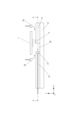
図1はインプリント装置を示した図である。インプリント装置1(成形装置)は、基板10上に供給されたインプリント材(組成物)と型7(原版、テンプレート)とを接触させる。そして、インプリント材9に硬化用のエネルギーを与えることにより、型7の凹凸パターンが転写された硬化物の組成物を成形する。
FIG. 1 is a diagram showing an imprint apparatus. The imprinting apparatus 1 (molding apparatus) brings the imprinting material (composition) supplied onto the
ここで、インプリント材には、硬化用のエネルギーが与えられることにより硬化する硬化性組成物(未硬化状態のインプリント材と呼ぶこともある)が用いられる。硬化用のエネルギーとしては、電磁波、熱等が用いられる。電磁波としては、例えば、その波長が150nm以上1mm以下の範囲から選択される、赤外線、可視光線、紫外線などの光である。 The imprint material used here is a curable composition (also referred to as an uncured imprint material) that cures when energy for curing is applied. Electromagnetic waves, heat, and the like are used as curing energy. The electromagnetic wave is, for example, light such as infrared rays, visible rays, and ultraviolet rays whose wavelengths are selected from the range of 150 nm or more and 1 mm or less.
硬化性組成物は、光の照射により、あるいは、加熱により硬化する組成物である。このうち、光により硬化する光硬化性組成物は、重合性化合物と光重合開始剤とを少なくとも含有し、必要に応じて非重合性化合物または溶剤を含有してもよい。非重合性化合物は、増感剤、水素供与体、内添型離型剤、界面活性剤、酸化防止剤、ポリマー成分などの群から選択される少なくとも一種である。 A curable composition is a composition that is cured by irradiation with light or by heating. Among these, the photocurable composition that is cured by light contains at least a polymerizable compound and a photopolymerization initiator, and may contain a non-polymerizable compound or a solvent if necessary. The non-polymerizable compound is at least one selected from the group consisting of sensitizers, hydrogen donors, internal release agents, surfactants, antioxidants, polymer components and the like.
インプリント材は、スピンコーターやスリットコーターにより基板上に膜状に付与される。或いは液体噴射ヘッドにより、液滴状、或いは複数の液滴が繋がってできた島状又は膜状となって基板上に付与されてもよい。インプリント材の粘度(25℃における粘度)は、例えば、1mPa・s以上100mPa・s以下である。 The imprint material is applied in the form of a film on the substrate by a spin coater or a slit coater. Alternatively, it may be applied onto the substrate in the form of droplets, or in the form of islands or films formed by connecting a plurality of droplets, by a liquid jet head. The viscosity of the imprint material (viscosity at 25° C.) is, for example, 1 mPa·s or more and 100 mPa·s or less.
本実施例では、インプリント装置1は、光の照射によりインプリント材を硬化させる光硬化法を採用するものとして説明する。また、以下では、基板上のインプリント材に対して光を照射する、後述の照射光学系の光軸に平行な方向をZ軸方向とし、Z軸方向に垂直な平面内で互いに直交する2方向をX軸方向及びY軸方向とする。
In this embodiment, the
図1を用いて、インプリント装置1の各部について説明する。型保持部3は、真空吸着力や静電気力によって型7を引き付けて保持する型チャック11と、型チャック11を保持して型7(型チャック11)を移動させる型移動機構12とを含む。型チャック11及び型移動機構12は、照射部2からの光が基板10の上のインプリント材9に照射されるように、中心部(内側)に開口を有する。型移動機構12は、基板10の上のインプリント材への型7の押し付け(押印)、又は、基板10の上のインプリント材9からの型7の引き離し(離型)を選択的に行うように、型7をZ軸方向に移動させる。型移動機構12に適用可能なアクチュエータは、例えば、リニアモータやエアシリンダを含む。型移動機構12は、型7を高精度に位置決めするために、粗動駆動系や微動駆動系などの複数の駆動系から構成されていても良い。また、型移動機構12は、Z軸方向だけではなく、X軸方向やY軸方向に型7を移動可能に構成されていても良い。更に、型移動機構12は、型7のθ(Z軸周りの回転)方向の位置や型7の傾きを調整するためのチルト機能を有するように構成されていても良い。
Each part of the
型7は、矩形の外周形状を有し、基板に対向する面(パターン面)に3次元状に形成されたパターン(回路パターンなどの基板10に転写すべき凹凸パターン)を備えたパターン部7aを有する。型7は、光を透過させることが可能な材料、例えば、石英で構成される。また、型7は、光8が照射される面に、平面形状が円形で、かつ、ある程度の深さのキャビティを有する場合もある。
The
照射部2は、光源(不図示)と照射光学系(不図示)を有し、照射光学系は後述の光学素子を組み合わせたものを備える。照射部2は、インプリント処理(成形処理)において、型7を介して、基板10の上のインプリント材に光8(例えば、紫外線)を照射する。照射部2は、光源と、光源からの光をインプリント処理に適切な光8の状態(光の強度分布、照明領域など)に調整するための光学素子(レンズ、ミラー、遮光板など)とを含む。本実施例では、光硬化法を採用しているため、インプリント装置1が照射部2を有している。但し、熱硬化法を採用する場合には、インプリント装置1は、照射部2に代えて、インプリント材(熱硬化性インプリント材)を硬化させるための熱源を有することになる。
The irradiation unit 2 has a light source (not shown) and an irradiation optical system (not shown), and the irradiation optical system is provided with a combination of optical elements to be described later. The irradiation unit 2 irradiates the imprint material on the
基板チャック14は、真空吸着力や静電気力によって基板10を引き付けて保持する。補助部材15は、基板チャック14に保持された基板10を取り囲むようにして、基板チャック14の周囲に配置されている。また、補助部材15の上面と基板チャック14に保持された基板10の上面とがほぼ同じ高さになるように、補助部材15が配置されている。基板チャック14はステージ駆動機構16上に搭載される。ここで、基板チャック14、ステージ駆動機構16を合わせて基板ステージ4(移動部)とする。基板ステージ4は、XY面内で移動可能である。型7のパターン部7aを基板10の上のインプリント材に押し付ける際に基板ステージ4の位置を調整することで型7の位置と基板10の位置とを互いに整合させる。基板ステージ4に適用可能なアクチュエータは、例えば、リニアモータやエアシリンダを含む。また、基板ステージ4は、X軸方向やY軸方向だけではなく、Z軸方向に基板10を移動可能に構成されていても良い。なお、インプリント装置1における型7の押印及び離型は、型7をZ軸方向に移動させることで実現する。ただし、基板10をZ軸方向に移動させることで実現させても良い。また、型7と基板10の双方を相対的にZ軸方向に移動させることで、型7の押印及び離型を実現しても良い。また、基板ステージ4は、基板10のθ(Z軸周りの回転)方向の位置や基板10の傾きを調整するためのチルト機能を有するように構成されていても良い。
The
また、基板ステージ4は、その側面に、X、Y、Z、ωx、ωy、ωzの各方向に対応した複数の参照ミラー17を備える。これに対して、インプリント装置1は、これらの参照ミラー17にそれぞれヘリウムネオンなどのビームを照射することで基板ステージ4の位置を測定する複数のレーザー干渉計18を備える。なお、図1では、参照ミラー17とレーザー干渉計18との1つの組のみを図示している。レーザー干渉計18は、基板ステージ4の位置を実時間で計測し、後述する制御部6は、このときの計測値に基づいて基板10(基板ステージ4)の位置決め制御を実行する。また、基板ステージ4の位置を計測するためにエンコーダを用いてもよい。
The substrate stage 4 also has a plurality of reference mirrors 17 on its side surfaces corresponding to the X, Y, Z, ωx, ωy, and ωz directions. On the other hand, the
補助部材15は、参照ミラー17とレーザー干渉計18との光路に後述の第1気体30が侵入しないようにさせる機能を有する。また、補助部材15があることにより、基板10の周辺に配置されるショット領域をインプイリントする際に、後述の第1気体供給部26から供給される気体の濃度を高く保つことができるという効果もある。ここで、補助部材15の上の空間と基板10の上の空間とで気体の濃度に1%以上の差が生じない限度で、補助部材15の上面の高さと基板チャック14に保持された基板10の上面の高さに差が生じていてもよい。例えば、補助部材15の上面と基板チャック14に保持された基板10の上面との高さの差は1mm以下であればよい。より好ましくは、補助部材15の上面と基板チャック14に保持された基板10の上面との高さの差は0.1mm以下であればよい。
The
基板10は、ガラス、セラミックス、金属、インプリント材等が用いられ、必要に応じて、その表面に基板とは別の材料からなる部材が形成されていてもよい。基板としては、具体的に、シリコンウエハ、化合物半導体ウエハ、石英を材料に含むガラスウエハなどである。また、基板は、インプリント処理によりマスターマスクからレプリカマスクを製造するためのガラス基板であっても良い。
Glass, ceramics, metal, imprint material, or the like is used for the
塗布部5(組成物供給部)は型保持部3の近傍に設置され、基板10上に存在する、少なくとも1つのショット領域(成形領域)にインプリント材9を塗布する。塗布部5は、塗布方式としてインクジェット方式を採用し、未硬化状態のインプリント材9を収容する容器19と、吐出部20とを含む。容器19は、その内部をインプリント材9の硬化反応を起こさないような、例えば若干の酸素を含む雰囲気としつつ、インプリント材9を管理可能とするものが望ましい。また、容器19の材質は、インプリント材9にパーティクルや化学的な不純物を混入させないようなものとすることが望ましい。吐出部20は、例えば複数の吐出口を含むピエゾタイプの吐出機構(インクジェットヘッド)を有する。インプリント材9の塗布量(吐出量)は、0.1~10pL/滴の範囲で調整可能であり、通常、約1pL/滴で使用する場合が多い。なお、インプリント材9の全塗布量は、パターン部7aの密度、および所望の残膜厚により決定される。塗布部5は、後述する制御部6からの動作指令に基づいて、インプリント材9を液滴としてショット上に分散させて塗布させ、塗布位置や塗布量などを制御する。
The application unit 5 (composition supply unit) is installed near the
アライメント計測部21は、基板10上に形成されているアライメントマークを計測する。また、インプリント装置1は、基板ステージ4を載置し基準平面を形成する定盤22と、型保持部3を固定するブリッジ定盤23と、定盤22から延設され、床面からの振動を除去する除振器24を介してブリッジ定盤23を支持する支柱25とを備える。さらに、インプリント装置1は、共に不図示であるが、型7を装置外部と型保持部3との間で搬入出させる型搬送部や、基板10を装置外部と基板ステージ4との間で搬入出させる基板搬送部などを含み得る。
The
制御部6は、CPUやメモリなどを含む、少なくとも1つのコンピュータで構成される。また、制御部6は、インプリント装置1の各構成要素に回線を介して接続され、メモリに格納されたプログラムに従って、インプリント装置1の各構成要素の動作及び調整などを制御する。また、制御部6は、インプリント装置1の他の部分と一体で(共通の筐体内に)構成してもよいし、インプリント装置1の他の部分とは別体で(別の筐体内に)構成してもよい。
The control unit 6 is composed of at least one computer including a CPU, memory, and the like. Also, the control unit 6 is connected to each component of the
ここで、インプリント装置1によるインプリント方法(インプリント処理)について説明する。まず、制御部6は、基板搬送部により基板ステージ4に基板10を載置および固定させる。次に、制御部6は、ステージ駆動機構16を駆動させて基板10の位置を適宜変更させつつ、アライメント計測部21により基板10上のアライメントマークを順次計測させ、基板10の位置を高精度に検出する。そして、制御部6は、その検出結果から各転写座標を演算し、この演算結果に基づいて所定のショットごとに逐次パターンを成形させる(ステップ・アンド・リピート)。ある1つのショット領域に対するパターン成形の流れとして、制御部6は、まず、ステージ駆動機構16により、吐出部20の吐出口の下に基板10上の塗布位置(ショット領域上の特定の位置)を位置決めさせる。その後、塗布部5は、基板10上のショット領域にインプリント材9を塗布する(塗布工程)。次に、制御部6は、ステージ駆動機構16により、パターン部7a直下の押し付け位置にショット領域が位置するように基板10を移動させ、位置決めさせる。次に、制御部6は、パターン部7aとショット領域上の基板側パターンとの位置合わせや倍率補正機構によるパターン部7aの倍率補正などを実施する。その後、型移動機構12を駆動させ、ショット領域上のインプリント材9にパターン部7aを押し付ける(押印工程)。この押し付けにより、インプリント材9は、パターン部7aの凹凸パターンに充填される。なお、制御部6は、押し付け完了の判断を型保持部3の内部に設置された不図示の荷重センサにより行う。この状態で、照射部2は、硬化工程として型7の背面(上面)から光8を所定時間照射し、型7を透過した光8によりインプリント材9を硬化させる。そして、インプリント材9が硬化した後、制御部6は、型移動機構12を再駆動させ、パターン部7aを基板10から引き離す(離型工程)。これにより、基板10上のショット領域の表面には、パターン部7aの凹凸パターンに倣った3次元形状のインプリント材パターン(層)が成形される。このような一連のインプリント動作を基板ステージ4の駆動によりショット領域を変更しつつ複数回実施することで、インプリント装置1は、1枚の基板10上に複数のインプリント材パターンを成形することができる。
Here, an imprinting method (imprinting process) by the
また、型7を基板10上のインプリント材9に押し付けて、パターン部7aにインプリント材9を充填させる際に、型7と基板10との間に存在する空気が、パターン部7aに入り込み、硬化後、成形されたパターンに不良の発生が生じ得る。そこで、型7と基板10との間の空間に、少なくともインプリント材9に対して高可溶性又は高拡散性のいずれか一方の性質を有する気体を供給させるとよい。
Further, when the
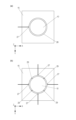
また、インプリント装置1は、気体を供給する第1気体供給部26、第2気体供給部27(いずれも図1では不図示)を備える。ここで、図2を用いて、第1気体供給部26、第2気体供給部27について説明する。図2は、第1気体供給部26、及び第2気体供給部27を示す図である。第1気体供給部26は、気体供給源(不図示)から配管を介して高可溶性又は高拡散性のいずれか一方の性質を有する気体(以下、第1気体30とする)を供給する。また、第1気体供給部26は、型7の周辺に配置された供給口から、型7と基板10との間の空間に、第1気体30を供給する。供給する第1気体30は、型7、インプリント材9、及び基板10の少なくとも1つに対して溶解又は拡散する性質を有する。例えば、第1気体30には、ヘリウムや二酸化炭素が含まれ得るが、これらに限られない。
The
第1気体供給部26は、型7の周辺に第1気体30を供給する。これにより型7の周辺において第1気体30の濃度が上昇し、第1気体30が持つ拡散効果により、型7と基板10との間の空間において第1気体30の濃度が上昇する。また、基板ステージ4のXY平面内に沿った移動を利用して、いわゆるコアンダ効果により、短時間で型7と基板10との間の空間における第1気体30の濃度を上昇させることができる。
The first
ここで、基板チャック14に保持された基板10と補助部材15との間隔は、基板10を基板チャック上に搬送する際の誤差を考慮して、約0.5mm~2.0mmとなるように補助部材15が配置される。より好ましくは、基板10と補助部材15との間隔が、約1.0mm~1.1mmとなるように補助部材15が配置されるとよい。これにより、基板10、基板チャック14(基板ステージ4)、補助部材15に囲まれた空間28が存在する。空間28には、空気等の高可溶性又は高拡散性のいずれの性質も有しない気体(以下、第2気体とする)が存在している。そのため、第1気体30が持つ拡散効果では第1気体30が空間28に第1気体30が十分に供給されず、空間28において第1気体30の濃度は十分に上がらない。また、基板ステージ4の移動によっても、空間28において第1気体30の濃度は十分に上がらない。また、空間28に第2気体が存在している状態で、基板10の周辺にあるショット領域上のインプリント材9に対してインプリント処理を行うと、空間28から第2気体が型7と基板10の間に入り、第2気体が気泡として残留して不良の発生が生じ得る。
Here, the distance between the
そこで、本実施例に係るインプリト装置1は、補助部材15に配置され、第1気体30を空間28に供給する第2気体供給部27を有する。第2気体供給部27は、第1気体供給部26と同様に、気体供給源(不図示)から配管を介して第1気体30を供給する。第2気体供給部27は、基板10の側面に対向する、補助部材15の側面から空間28に第1気体30を供給する供給口を有する。第2気体供給部27が空間28に第1気体30を供給することにより、空間28において第1気体30の濃度を上げることができる。これにより、周辺のショット領域において不良の発生を低減することができる。また、第2気体供給部27の供給口には、第1気体30の供給により異物の巻き上げや局所的な圧力の上昇を低減するために、多孔質やメッシュ形状の部材が備えられるとよい。
Therefore, the
図3は、図2のA-A’で示す面を上から見た、第2気体供給部27を示す断面図である。図3(a)に示す第2気体供給部27は、補助部材15の側面の1箇所に供給口を有する。図3(b)に示す第2気体供給部27は、補助部材15の側面に複数の供給口を有する。これにより、図3(a)に示す第2気体供給部27よりも、図3(b)に示す第2気体供給部27の方が、短時間で空間28における第1気体30の濃度を上げることができる。また、図3(b)に示す第2気体供給部27は、インプリント処理を行うショット領域の位置に応じて、第2気体供給部27の供給口を切り替えて第1気体30を供給してもよい。これにより、第2気体供給部27から供給する第1気体30を削減することができる。また、図3(b)に示すように、空間28を仕切る仕切り部材29を設けてもよい。仕切り部材29は、空間28を第2気体供給部27の複数の供給口に対応した数の空間に分けるように配置する。これにより、さらに短時間に空間28における第1気体30の濃度を上げることができる。
FIG. 3 is a cross-sectional view showing the second
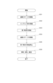
次に、インプリント処理における第1気体30の供給方法について、図4、及び図5を用いて説明する。図4は、基板ステージ4、第1気体供給部26、及び第2気体供給部27の動作を示す図である。また、図5は、基板ステージ4、第1気体供給部26、及び第2気体供給部27の動作を示すフローチャートである。まず、S501において、制御部6は、基板10のショット領域が吐出部20(塗布部5)と対向する位置に、基板ステージ4を移動させる。そして、S502において、制御部6は、塗布部5に吐出部20から基板10のショット領域にインプリント材9を供給させる(図4(a))。そして、S503において、制御部6は、第1気体供給部26により第1気体30を供給させる(図4(b))。また、制御部6は、第2気体供給部27により第1気体30を供給させる(図4(b))。このとき、制御部6は、第2気体供給部27により、インプリント材9が供給されたショット領域の近傍の供給口から第1気体30を供給させる。そして、S504において、制御部6は、インプリント材9が供給されたショット領域が型7(型保持部3)と対向する位置に、基板ステージ4を移動させる(図4(c))。このとき、第1気体30は基板10と型7の間の空間及び、空間28に供給された状態であり、それぞれの空間において、第1気体30の濃度は十分に上昇している状態である。そして、S505において、制御部6は、第1気体供給部26、及び第2気体供給部27に第1気体30の供給を停止させる。そして、S506において、インプリント材9を供給したショット領域に対して、押印、硬化、離型が行われる。ここで、基板10の複数のショット領域をインプリント処理する場合は、所定の回数だけS501からS506を繰り返す。また、周辺にあるショット領域以外のショット領域に対してインプリント処理を行う場合には、供給する第1気体30の量を削減するために第2気体供給部27から第1気体30の供給を行わなくてもよい。
Next, a method of supplying the
以上により、本実施例に係るインプリト装置によれば、基板の周辺部における不良の発生を低減できる。 As described above, according to the imprint apparatus according to the present embodiment, it is possible to reduce the occurrence of defects in the peripheral portion of the substrate.
次に実施例2に係るインプリント装置について説明する。なお、ここで言及しない事項は、実施例1に従い得る。 Next, an imprint apparatus according to a second embodiment will be described. Matters not mentioned here can follow the first embodiment.
図6は、実施例2に係る第1気体供給部26、及び第2気体供給部27を示す図である。第1気体供給部26は、実施例1と同様に、型7の周辺に配置され、型7と基板10との間の空間に、第1気体30を供給する。第2気体供給部27は、実施例1とは異なり、基板ステージ4(基板チャック14)に配置される。また、第2気体供給部27の供給口は、基板10の側面と補助部材15の間の基板ステージ4(基板チャック14)の上面に配置される。第2気体供給部27が空間28に第1気体30を供給することにより、空間28において第1気体30の濃度を上げることができる。これにより、周辺にあるショット領域における不良の発生を低減することができる。また、第2気体供給部27の供給口には、第1気体30の供給により異物の巻き上げや局所的な圧力の上昇を低減するために、多孔質やメッシュ形状の部材が備えられるとよい。また、実施例1と同様に、第2気体供給部27の供給口は複数、配置しても良く、空間28を仕切る仕切り部材29を配置してもよい。
FIG. 6 is a diagram showing the first
また、第2気体供給部27の供給口の直径を約1mm~2mmとすると、基板チャック14に保持された基板10と補助部材15との間隔は、約3.0mm~4.0mmとなるように補助部材15が配置されるとよい。より好ましくは、基板10と補助部材15との間隔が、約1.1mm~2.1mmとなるように補助部材15が配置されているとよい。
When the diameter of the supply port of the second
以上により、本実施例に係るインプリト装置によれば、基板の周辺部における不良の発生を低減できる。 As described above, according to the imprint apparatus according to the present embodiment, it is possible to reduce the occurrence of defects in the peripheral portion of the substrate.
次に実施例3に係るインプリント装置について説明する。なお、ここで言及しない事項は、実施例1、及び2に従い得る。 Next, an imprint apparatus according to a third embodiment will be described. Matters not mentioned here can follow Examples 1 and 2.
図7は、実施例3に係る第1気体供給部26、及び第2気体供給部27を示す図である。第1気体供給部26は、実施例1と同様に、型7の周辺に配置され、型7と基板10との間の空間に、第1気体30を供給する。第2気体供給部27は、実施例2と同様に、基板ステージ4(基板チャック14)に配置される。また、第2気体供給部27の供給口は、基板10の側面と補助部材15の間の基板ステージ4(基板チャック14)の上面に配置される。第2気体供給部27が空間28に第1気体30を供給することにより、空間28において第1気体30の濃度を上げることができる。さらに、第2気体供給部27の供給口の上を覆うように、補助部材15に遮蔽部材31が配置される。遮蔽部材31は、第2気体供給部27により供給される第1気体の気流を遮蔽して、第1気体の気流により巻き上げられた異物が補助部材15の上面より上の空間に飛散して、基板10や型7などに付着することを抑制することができる。また、遮蔽部材31を配置することにより第2気体供給部27から供給された第1気体30の濃度が短時間で上昇するという効果も得られる。これにより、周辺にあるショット領域における不良の発生を低減することができる。また、第2気体供給部27の供給口には、第1気体30の供給により異物の巻き上げや局所的な圧力の上昇を低減するために、多孔質やメッシュ形状の部材が備えられるとよい。
FIG. 7 is a diagram showing the first
また、実施例2と同様に、基板チャック14に保持された基板10と補助部材15との間隔が、約3.0mm~4.0mmとなるように補助部材15が配置されるとよい。また、基板チャック14に保持された基板10と遮蔽部材31との間隔が、約1.0mm~1.1mmとなるように遮蔽部材31が配置されるとよい。
Further, as in the second embodiment, the
また、本実施例では、第2気体供給部27の供給口は、実施例2と同様に基板ステージ4に配置されるが、実施例1のように第2気体供給部27の供給口が補助部材15に配置される形態において、本実施例の遮蔽部材31を配置してもよい。
In this embodiment, the supply port of the second
以上により、本実施例に係るインプリト装置によれば、基板の周辺部における不良の発生を低減できる。 As described above, according to the imprint apparatus according to the present embodiment, it is possible to reduce the occurrence of defects in the peripheral portion of the substrate.
(物品の製造方法)
インプリント装置を用いて成形した硬化物のパターンは、各種物品の少なくとも一部に恒久的に、或いは各種物品を製造する際に一時的に、用いられる。物品とは、電気回路素子、光学素子、MEMS、記録素子、センサ、或いは、型等である。電気回路素子としては、DRAM、SRAM、フラッシュメモリ、MRAMのような、揮発性或いは不揮発性の半導体メモリや、LSI、CCD、イメージセンサ、FPGAのような半導体素子等が挙げられる。型としては、インプリント用のモールド等が挙げられる。
(Product manufacturing method)
A pattern of a cured product formed using an imprint apparatus is used permanently on at least a part of various articles, or temporarily used when manufacturing various articles. Articles are electric circuit elements, optical elements, MEMS, recording elements, sensors, molds, or the like. Examples of electric circuit elements include volatile or nonvolatile semiconductor memories such as DRAM, SRAM, flash memory, and MRAM, and semiconductor elements such as LSI, CCD, image sensors, and FPGA. Examples of the mold include imprint molds and the like.
硬化物のパターンは、上記物品の少なくとも一部の構成部材として、そのまま用いられるか、或いは、レジストマスクとして一時的に用いられる。基板の加工工程においてエッチング又はイオン注入等が行われた後、レジストマスクは除去される。 The pattern of the cured product is used as it is or temporarily used as a resist mask as at least a part of the article. After etching, ion implantation, or the like in the substrate processing step, the resist mask is removed.
次に、物品の具体的な製造方法について説明する。図8(a)に示すように、絶縁体等の被加工材2zが表面に成形されたシリコンウエハ等の基板1zを用意し、続いて、インクジェット法等により、被加工材2zの表面にインプリント材3zを付与する。ここでは、複数の液滴状になったインプリント材3zが基板上に付与された様子を示している。 Next, a specific manufacturing method for the article will be described. As shown in FIG. 8A, a substrate 1z such as a silicon wafer having a surface to be processed 2z such as an insulator formed thereon is prepared. A printing material 3z is applied. Here, a state is shown in which a plurality of droplet-like imprint materials 3z are applied onto the substrate.
図8(b)に示すように、インプリント用の型4zを、その凹凸パターンが成形された側を基板上のインプリント材3zに向け、対向させる。図8(c)に示すように、インプリント材3zが付与された基板1zと型4zとを接触させ、圧力を加える。インプリント材3zは型4zと被加工材2zとの隙間に充填される。この状態で硬化用のエネルギーとして光を型4zを透して照射すると、インプリント材3zは硬化する。 As shown in FIG. 8(b), the imprint mold 4z is opposed to the imprint material 3z on the substrate with the side on which the uneven pattern is formed. As shown in FIG. 8(c), the substrate 1z provided with the imprint material 3z and the mold 4z are brought into contact with each other and pressure is applied. The imprint material 3z is filled in the gap between the mold 4z and the workpiece 2z. In this state, when light is irradiated through the mold 4z as energy for curing, the imprint material 3z is cured.
図8(d)に示すように、インプリント材3zを硬化させた後、型4zと基板1zを引き離すと、基板1z上にインプリント材3zの硬化物のパターンが成形される。この硬化物のパターンは、型の凹部が硬化物の凸部に、型の凹部が硬化物の凸部に対応した形状になっており、即ち、インプリント材3zに型4zの凹凸パターンが転写されたことになる。 As shown in FIG. 8D, after the imprint material 3z is cured, the mold 4z and the substrate 1z are separated to form a pattern of the cured imprint material 3z on the substrate 1z. The pattern of this cured product has a shape in which the concave portions of the mold correspond to the convex portions of the cured product, and the concave portions of the mold correspond to the convex portions of the cured product. It will be done.
図8(e)に示すように、硬化物のパターンを耐エッチングマスクとしてエッチングを行うと、被加工材2zの表面のうち、硬化物が無いか或いは薄く残存した部分が除去され、溝5zとなる。図8(f)に示すように、硬化物のパターンを除去すると、被加工材2zの表面に溝5zが成形された物品を得ることができる。ここでは硬化物のパターンを除去したが、加工後も除去せずに、例えば、半導体素子等に含まれる層間絶縁用の膜、つまり、物品の構成部材として利用してもよい。
As shown in FIG. 8(e), when etching is performed using the pattern of the cured product as an anti-etching mask, the portion of the surface of the workpiece 2z where the cured product is absent or remains thinly is removed, forming the
なお、型4zとして、凹凸パターンを設けた回路パターン転写用の型を用いた例について述べたが、凹凸パターンがない平面部を有する型(ブランクテンプレート)であってもよい。ブランクテンプレートは、平面部によって基板上の組成物を平坦化するように成形する平坦化処理(成形処理)を行う平坦化装置(成形装置)に用いられる。平坦化処理は、基板上に供給された組成物にブランクテンプレートの平坦部を接触させた状態で、光の照射によって、或いは、加熱によって組成物を硬化させる工程を含む。 As the mold 4z, an example of using a mold for transferring a circuit pattern provided with an uneven pattern has been described, but a mold (blank template) having a flat portion without an uneven pattern may also be used. The blank template is used in a flattening apparatus (molding apparatus) that performs a flattening process (molding process) to flatten the composition on the substrate using a flat portion. The planarization process includes a step of curing the composition by light irradiation or heating while the flat portion of the blank template is in contact with the composition supplied on the substrate.
以上、本発明の好ましい実施形態について説明したが、本発明はこれらの実施形態に限定されないことはいうまでもなく、その要旨の範囲内で種々の変形および変更が可能である。 Although the preferred embodiments of the present invention have been described above, it goes without saying that the present invention is not limited to these embodiments, and various modifications and changes can be made within the scope of the gist thereof.
成形装置の一例として、基板の上のインプリント材を型により成形(成型)して、基板にパターン成形を行うインプリント装置について説明したが、インプリント装置に限定されるものではない。成形装置の一例として、型として凹凸パターンがない平面部を有する型(ブランクテンプレート)を用いて、基板上の組成物を平坦化するように成形する平坦化処理(成形処理)を行う平坦化装置であっても良い。 As an example of a molding apparatus, an imprinting apparatus that molds (molds) an imprinting material on a substrate to form a pattern on the substrate has been described, but the imprinting apparatus is not limited to the imprinting apparatus. As an example of a molding apparatus, a flattening apparatus that performs a flattening process (molding process) for flattening a composition on a substrate using a mold (blank template) having a flat portion without an uneven pattern. can be
また、実施例1乃至3は、単独で実施するだけでなく、実施例1乃至3のいずれかを組合せて実施することができる。 In addition, Examples 1 to 3 can be implemented not only independently, but also in combination with any of Examples 1 to 3.
Claims (20)
前記型を保持する型保持部と、
前記基板を保持して移動する移動部と、
前記基板に対して上方から前記基板と前記型の間に所定の気体を供給する第1の供給口と、
前記基板の側面と前記移動部の上面を含む複数の面で囲まれた空間に前記所定の気体を供給する第2の供給口と、
前記第1の供給口と前記第2の供給口からの前記所定の気体の供給を制御する制御部と、を有し、
前記第1の供給口は、前記型保持部の周辺に配置されていて、
前記第2の供給口は、前記空間を挟んで前記基板の側面に対面する位置、または前記空間の下側に配置されていて、
前記制御部は、前記基板上の成形領域に前記組成物が供給された前記基板を前記移動部が保持して移動する時に、前記第1の供給口と前記第2の供給口の両方から前記所定の気体を供給する制御を行うことを特徴とする成形装置。 A molding apparatus for molding a composition on a substrate using a mold,
a mold holding part that holds the mold;
a moving part that holds and moves the substrate;
a first supply port that supplies a predetermined gas between the substrate and the mold from above the substrate;
a second supply port that supplies the predetermined gas to a space surrounded by a plurality of surfaces including the side surface of the substrate and the upper surface of the moving part;
a controller for controlling supply of the predetermined gas from the first supply port and the second supply port;
The first supply port is arranged around the mold holding part,
The second supply port is arranged at a position facing the side surface of the substrate across the space or below the space,
When the moving part holds and moves the substrate to which the composition has been supplied to the molding region on the substrate, the control unit controls the composition from both the first supply port and the second supply port. A molding apparatus characterized by performing control to supply a predetermined gas.
前記複数の空間のそれぞれに少なくとも1つの前記第2の供給口が配置されていることを特徴とする、請求項8に記載の成形装置。 the moving part has a partition member that partitions a plurality of spaces between the substrate held by the moving part and the auxiliary member;
9. The molding apparatus according to claim 8, wherein at least one said second supply port is arranged in each of said plurality of spaces.
前記制御部は、前記移動部が前記成形領域を前記組成物供給部と対向する位置から前記型保持部に対向する位置に移動させている間に、前記第2の供給口は前記所定の気体を供給するよう制御することを特徴とする、請求項11又は12に記載の成形装置。 having a composition supply unit that supplies the composition to a molding region on the substrate;
While the moving part moves the molding area from a position facing the composition supply part to a position facing the mold holding part, the control part is configured to cause the second supply port to move the predetermined gas. 13. The molding apparatus according to claim 11 or 12, characterized in that it is controlled to supply .
前記基板の周辺部以外の成形領域に前記組成物が供給された場合、前記移動部が前記基板を移動させている間に前記第2の供給口から前記所定の気体を供給しないよう制御することを特徴とする1~15のうちいずれか1項に記載の成形装置。 When the composition is supplied to the molding region in the peripheral portion of the substrate, the control unit supplies a predetermined gas from the second supply port while the substrate is held and moved by the moving unit. to supply
When the composition is supplied to a molding region other than the peripheral portion of the substrate, controlling so that the predetermined gas is not supplied from the second supply port while the moving unit is moving the substrate. 16. The molding apparatus according to any one of 1 to 15, characterized by:
前記基板を保持して移動する移動部と、
前記移動部に保持され、前記基板の側面と前記移動部の上面を含む複数の面で囲まれた空間に所定の気体を供給する供給口を含み、該供給口から前記所定の気体を供給する気体供給部と、
前記気体供給部を制御する制御部と、を備え、
前記移動部は、前記供給口の上を覆う遮蔽部材を有しており、
前記制御部は、前記基板上の周辺の成形領域に前記組成物が供給された前記基板を前記移動部が移動させている間に、前記供給口から前記所定の気体を供給することを特徴とする成形装置。 A molding apparatus for molding a composition on a substrate using a mold,
a moving part that holds and moves the substrate;
A supply port that is held by the moving part and that supplies a predetermined gas to a space surrounded by a plurality of surfaces including a side surface of the substrate and an upper surface of the moving part, and supplies the predetermined gas from the supply port. a gas supply;
A control unit that controls the gas supply unit,
The moving part has a shielding member covering the supply port,
The control unit supplies the predetermined gas from the supply port while the moving unit is moving the substrate supplied with the composition to a molding region on the periphery of the substrate. molding equipment.
組成物供給部により前記基板上の周辺の成形領域に組成物を供給する第1供給工程と、
前記基板を保持して移動する移動部により前記成形領域を前記組成物供給部と対向する位置から前記型を保持する型保持部に対向する位置に移動させる移動工程と、
前記型保持部の周辺に配置され前記基板に対して上方から前記基板と前記型の間に所定の気体を供給する第1の供給口と、前記基板の側面と前記移動部の上面を含む複数の面で囲まれた空間を挟んで前記基板の側面に対面する位置、または前記空間の下側に配置され前記空間に前記所定の気体を供給する第2の供給口の両方から、前記移動工程において前記基板を移動させている間に前記所定の気体を供給する第2供給工程と、
前記基板上の周辺の成形領域に前記型を用いて前記組成物を成形する成形工程と、を有することを特徴とする成形方法。 A molding method for molding a composition on a substrate using a mold,
a first supply step of supplying a composition to a peripheral molding region on the substrate by a composition supply unit;
a moving step of moving the molding region from a position facing the composition supply section to a position facing a mold holding section holding the mold by a moving section that holds and moves the substrate;
a plurality of first supply ports arranged around the mold holding part for supplying a predetermined gas between the substrate and the mold from above; from both the position facing the side surface of the substrate across the space surrounded by the plane of a second supply step of supplying the predetermined gas while moving the substrate in
and a molding step of molding the composition in a peripheral molding region on the substrate using the mold.
組成物供給部により前記基板上の周辺の成形領域に前記組成物を供給する第1供給工程と、
前記基板を保持して移動する移動部により前記成形領域を前記組成物供給部と対向する位置から前記型を保持する型保持部に対向する位置に移動させる移動工程と、
前記基板上の周辺の成形領域に前記組成物が供給された場合に前記移動工程において前記基板を移動させている間に、前記基板の側面と前記移動部の上面を含む複数の面で囲まれた空間に所定の気体を供給する、上を遮蔽部材で覆われた供給口から、前記所定の気体を供給する第2供給工程と、
前記基板上の周辺の成形領域に前記型を用いて前記組成物を成形する成形工程と、を有することを特徴とする成形方法。 A molding method for molding a composition on a substrate using a mold,
a first supply step of supplying the composition to a peripheral molding region on the substrate by a composition supply unit;
a moving step of moving the molding region from a position facing the composition supply section to a position facing a mold holding section holding the mold by a moving section that holds and moves the substrate;
While the substrate is being moved in the moving step when the composition is supplied to the peripheral molding region on the substrate, a plurality of surfaces including the side surface of the substrate and the top surface of the moving portion may be formed. a second supply step of supplying a predetermined gas to the space, which is supplied from a supply port covered with a shielding member;
and a molding step of molding the composition in a peripheral molding region on the substrate using the mold.
前記組成物が成形された前記基板を処理する処理工程と、
前記処理工程において処理された前記基板から物品を製造する製造工程と、を有することを特徴とする物品の製造方法。 A molding method according to claim 18 or 19;
a processing step of processing the substrate on which the composition has been molded;
and a manufacturing step of manufacturing an article from the substrate processed in the processing step.
Priority Applications (3)
| Application Number | Priority Date | Filing Date | Title |
|---|---|---|---|
| JP2018085318A JP7262930B2 (en) | 2018-04-26 | 2018-04-26 | Molding apparatus for molding composition on substrate using mold, molding method, and article manufacturing method |
| KR1020190044217A KR102401007B1 (en) | 2018-04-26 | 2019-04-16 | Molding apparatus that molds composition on substrate by using mold, molding method, and manufacturing method of article |
| US16/389,811 US11693308B2 (en) | 2018-04-26 | 2019-04-19 | Molding apparatus that molds composition on substrate by using mold, molding method, and manufacturing method of article |
Applications Claiming Priority (1)
| Application Number | Priority Date | Filing Date | Title |
|---|---|---|---|
| JP2018085318A JP7262930B2 (en) | 2018-04-26 | 2018-04-26 | Molding apparatus for molding composition on substrate using mold, molding method, and article manufacturing method |
Publications (3)
| Publication Number | Publication Date |
|---|---|
| JP2019192821A JP2019192821A (en) | 2019-10-31 |
| JP2019192821A5 JP2019192821A5 (en) | 2021-05-20 |
| JP7262930B2 true JP7262930B2 (en) | 2023-04-24 |
Family
ID=68292122
Family Applications (1)
| Application Number | Title | Priority Date | Filing Date |
|---|---|---|---|
| JP2018085318A Active JP7262930B2 (en) | 2018-04-26 | 2018-04-26 | Molding apparatus for molding composition on substrate using mold, molding method, and article manufacturing method |
Country Status (3)
| Country | Link |
|---|---|
| US (1) | US11693308B2 (en) |
| JP (1) | JP7262930B2 (en) |
| KR (1) | KR102401007B1 (en) |
Citations (8)
| Publication number | Priority date | Publication date | Assignee | Title |
|---|---|---|---|---|
| JP2012039057A (en) | 2010-07-13 | 2012-02-23 | Canon Inc | Imprint apparatus and method of manufacturing article |
| JP2015138842A (en) | 2014-01-21 | 2015-07-30 | キヤノン株式会社 | Imprint device and method of manufacturing article |
| JP2016092198A (en) | 2014-11-04 | 2016-05-23 | キヤノン株式会社 | Imprint device and method and product manufacturing method |
| JP2016219679A (en) | 2015-05-25 | 2016-12-22 | 株式会社東芝 | Substrate flattening method and method for calculating dropping amount |
| JP2017103399A (en) | 2015-12-03 | 2017-06-08 | キヤノン株式会社 | Imprint apparatus and article manufacturing method |
| JP2017199876A (en) | 2016-04-28 | 2017-11-02 | キヤノン株式会社 | Imprint method and manufacturing method of article |
| JP2017208424A (en) | 2016-05-17 | 2017-11-24 | キヤノン株式会社 | Imprint device and manufacturing method of article |
| JP2018029101A (en) | 2016-08-16 | 2018-02-22 | キヤノン株式会社 | Imprint device and article manufacturing method |
Family Cites Families (9)
| Publication number | Priority date | Publication date | Assignee | Title |
|---|---|---|---|---|
| US7377764B2 (en) * | 2005-06-13 | 2008-05-27 | Asml Netherlands B.V. | Imprint lithography |
| JP4892026B2 (en) * | 2009-03-19 | 2012-03-07 | 株式会社東芝 | Pattern formation method |
| JP5828626B2 (en) | 2010-10-04 | 2015-12-09 | キヤノン株式会社 | Imprint method |
| JP5647029B2 (en) | 2011-02-18 | 2014-12-24 | キヤノン株式会社 | Imprint apparatus and article manufacturing method |
| KR101249933B1 (en) * | 2011-08-02 | 2013-04-03 | (재)한국나노기술원 | Micro-Nano Hybrid Patterned Stamp Using Micro Patterned Stamp for Imprint Lithography and Method of Manufacturing for the Same |
| JP5787691B2 (en) * | 2011-09-21 | 2015-09-30 | キヤノン株式会社 | Imprint apparatus and article manufacturing method using the same |
| JP6021606B2 (en) * | 2011-11-28 | 2016-11-09 | キヤノン株式会社 | Imprint apparatus, article manufacturing method using the same, and imprint method |
| JP2013251462A (en) * | 2012-06-01 | 2013-12-12 | Canon Inc | Imprint device and manufacturing method of goods |
| JP5776631B2 (en) * | 2012-06-04 | 2015-09-09 | ウシオ電機株式会社 | Template cleaning method, pattern forming method, optical cleaning apparatus, and nanoimprint apparatus |
-
2018
- 2018-04-26 JP JP2018085318A patent/JP7262930B2/en active Active
-
2019
- 2019-04-16 KR KR1020190044217A patent/KR102401007B1/en active IP Right Grant
- 2019-04-19 US US16/389,811 patent/US11693308B2/en active Active
Patent Citations (8)
| Publication number | Priority date | Publication date | Assignee | Title |
|---|---|---|---|---|
| JP2012039057A (en) | 2010-07-13 | 2012-02-23 | Canon Inc | Imprint apparatus and method of manufacturing article |
| JP2015138842A (en) | 2014-01-21 | 2015-07-30 | キヤノン株式会社 | Imprint device and method of manufacturing article |
| JP2016092198A (en) | 2014-11-04 | 2016-05-23 | キヤノン株式会社 | Imprint device and method and product manufacturing method |
| JP2016219679A (en) | 2015-05-25 | 2016-12-22 | 株式会社東芝 | Substrate flattening method and method for calculating dropping amount |
| JP2017103399A (en) | 2015-12-03 | 2017-06-08 | キヤノン株式会社 | Imprint apparatus and article manufacturing method |
| JP2017199876A (en) | 2016-04-28 | 2017-11-02 | キヤノン株式会社 | Imprint method and manufacturing method of article |
| JP2017208424A (en) | 2016-05-17 | 2017-11-24 | キヤノン株式会社 | Imprint device and manufacturing method of article |
| JP2018029101A (en) | 2016-08-16 | 2018-02-22 | キヤノン株式会社 | Imprint device and article manufacturing method |
Also Published As
| Publication number | Publication date |
|---|---|
| US11693308B2 (en) | 2023-07-04 |
| JP2019192821A (en) | 2019-10-31 |
| US20190332007A1 (en) | 2019-10-31 |
| KR20190124643A (en) | 2019-11-05 |
| KR102401007B1 (en) | 2022-05-24 |
Similar Documents
| Publication | Publication Date | Title |
|---|---|---|
| KR101698253B1 (en) | Imprint apparatus and imprint method, and article manufacturing method | |
| JP6300459B2 (en) | Imprint apparatus, imprint method, and article manufacturing method using the same | |
| KR102011558B1 (en) | Imprint apparatus, imprint method, and method of manufacturing article | |
| US11556054B2 (en) | Forming apparatus, determination method, and article manufacturing method | |
| JP2018093122A (en) | Imprint device, and article manufacturing method | |
| JP2019145786A (en) | Imprint apparatus, planarization layer forming apparatus, forming apparatus, control method, and article manufacturing method | |
| JP6395352B2 (en) | Imprint apparatus, imprint method, and article manufacturing method using the same | |
| JP7171394B2 (en) | Molding Apparatus, Molding Method, and Article Manufacturing Method | |
| JP7262930B2 (en) | Molding apparatus for molding composition on substrate using mold, molding method, and article manufacturing method | |
| JP6304921B2 (en) | Imprint method, imprint apparatus, and article manufacturing method using the same | |
| JP7112249B2 (en) | DATA GENERATION METHOD, PATTERN FORMATION METHOD, IMPRINT APPARATUS, AND ARTICLE MANUFACTURING METHOD | |
| JP7064310B2 (en) | Imprinting equipment and article manufacturing method | |
| KR20210065854A (en) | Imprinting apparatus, imprinting method, method for producing article, substrate, and mold | |
| JP2021034562A (en) | Imprinting device, imprinting method, and article manufacturing method | |
| US20230063974A1 (en) | Molding apparatus, molding method, and method for manufacturing a product | |
| JP7267783B2 (en) | Flattening apparatus, flattening method and article manufacturing method | |
| JP7325232B2 (en) | Film forming apparatus and article manufacturing method | |
| US20210311386A1 (en) | Imprint apparatus, imprint method, and article manufacturing method | |
| JP2023179278A (en) | Molding device, imprint device, and manufacturing method of article | |
| JP2023180038A (en) | Film formation method, film formation device and article manufacturing method | |
| JP2022187398A (en) | Imprint device, imprint method, computer program, and method for manufacturing article | |
| JP2023056322A (en) | Substrate conveying method, substrate conveying device, and method for manufacturing article | |
| KR20220056795A (en) | Molding method, molding apparatus, molding system, and article manufacturing method | |
| JP2022002243A (en) | Molding device, molding method, and article manufacturing method | |
| JP2023109248A (en) | Imprint device, imprint method, and manufacturing method of article |
Legal Events
| Date | Code | Title | Description |
|---|---|---|---|
| A521 | Request for written amendment filed |
Free format text: JAPANESE INTERMEDIATE CODE: A523 Effective date: 20210408 |
|
| A621 | Written request for application examination |
Free format text: JAPANESE INTERMEDIATE CODE: A621 Effective date: 20210408 |
|
| A977 | Report on retrieval |
Free format text: JAPANESE INTERMEDIATE CODE: A971007 Effective date: 20220126 |
|
| A131 | Notification of reasons for refusal |
Free format text: JAPANESE INTERMEDIATE CODE: A131 Effective date: 20220201 |
|
| A521 | Request for written amendment filed |
Free format text: JAPANESE INTERMEDIATE CODE: A523 Effective date: 20220330 |
|
| A131 | Notification of reasons for refusal |
Free format text: JAPANESE INTERMEDIATE CODE: A131 Effective date: 20220712 |
|
| A521 | Request for written amendment filed |
Free format text: JAPANESE INTERMEDIATE CODE: A523 Effective date: 20220809 |
|
| A131 | Notification of reasons for refusal |
Free format text: JAPANESE INTERMEDIATE CODE: A131 Effective date: 20221025 |
|
| A521 | Request for written amendment filed |
Free format text: JAPANESE INTERMEDIATE CODE: A523 Effective date: 20221214 |
|
| TRDD | Decision of grant or rejection written | ||
| A01 | Written decision to grant a patent or to grant a registration (utility model) |
Free format text: JAPANESE INTERMEDIATE CODE: A01 Effective date: 20230314 |
|
| A61 | First payment of annual fees (during grant procedure) |
Free format text: JAPANESE INTERMEDIATE CODE: A61 Effective date: 20230412 |
|
| R151 | Written notification of patent or utility model registration |
Ref document number: 7262930 Country of ref document: JP Free format text: JAPANESE INTERMEDIATE CODE: R151 |