JP7257883B2 - Plasma processing method and plasma processing apparatus - Google Patents
Plasma processing method and plasma processing apparatus Download PDFInfo
- Publication number
- JP7257883B2 JP7257883B2 JP2019097691A JP2019097691A JP7257883B2 JP 7257883 B2 JP7257883 B2 JP 7257883B2 JP 2019097691 A JP2019097691 A JP 2019097691A JP 2019097691 A JP2019097691 A JP 2019097691A JP 7257883 B2 JP7257883 B2 JP 7257883B2
- Authority
- JP
- Japan
- Prior art keywords
- layer
- plasma processing
- film
- recess
- substrate
- Prior art date
- Legal status (The legal status is an assumption and is not a legal conclusion. Google has not performed a legal analysis and makes no representation as to the accuracy of the status listed.)
- Active
Links
Images


Landscapes
- Drying Of Semiconductors (AREA)
- Plasma Technology (AREA)
- Chemical Vapour Deposition (AREA)
- Formation Of Insulating Films (AREA)
Description
以下の開示は、プラズマ処理方法およびプラズマ処理装置に関する。 The following disclosure relates to plasma processing methods and plasma processing apparatuses.
半導体装置のパターン形成にALD(Atomic Layer Deposition)を含む様々な技術が利用されている。たとえば、被処理基板に形成される開口部の位置に応じて成膜が選択的に促進されるようにALDを利用した手法が提案されている(特許文献1)。また、SAM(Self-assembled monolayer: 自己組織化単分子膜)を選択的に形成し、その後、気相エッチングを行う手法が提案されている(特許文献2)。また、イオン注入を用いて3Dナノ構造体に対する選択的な成膜を実現する手法が提案されている(非特許文献1)。 Various techniques including ALD (Atomic Layer Deposition) are used for patterning semiconductor devices. For example, a method using ALD has been proposed so that film formation is selectively promoted according to the position of an opening formed in a substrate to be processed (Patent Document 1). Also, a method of selectively forming a SAM (Self-assembled monolayer) and then performing vapor phase etching has been proposed (Patent Document 2). In addition, a method of selectively forming a film on a 3D nanostructure using ion implantation has been proposed (Non-Patent Document 1).
半導体装置の製造においては、成膜およびエッチングの処理が実行される。この過程で、既に形成されたパターンが後の工程においてダメージを受ける可能性がある。 2. Description of the Related Art In the manufacture of semiconductor devices, film formation and etching processes are performed. In this process, already formed patterns may be damaged in subsequent processes.
本開示は、プラズマ処理においてパターンに与えるダメージを低減することができる技術を提供する。 The present disclosure provides a technique capable of reducing damage to patterns in plasma processing.
本開示の一態様によるプラズマ処理装置が実行するプラズマ処理方法は、開口部形成工程と、第1膜形成工程と、第2膜形成工程と、エッチング工程と、を含む。プラズマ処理装置は、開口部形成工程において、下地層と下地層上に形成される第1層とを含む処理対象基板に対してエッチングを施すことにより、第1層に開口部を形成する。プラズマ処理装置は、開口部が所定条件を満足したと判定した場合、第1膜形成工程において、化学気相成長(Chemical Vapor Deposition: CVD)により、開口部の底面にインヒビターを形成することで所定のガス種が吸着しない第1の膜を形成する。プラズマ処理装置は、第1の膜の形成後、第2膜形成工程において、所定のガス種を前駆体ガスとする原子層堆積(Atomic Layer Deposition: ALD)により開口部の側壁に第2の膜を形成する。プラズマ処理装置はさらに、エッチング工程において開口部にエッチングを施す。 A plasma processing method performed by a plasma processing apparatus according to an aspect of the present disclosure includes an opening forming process, a first film forming process, a second film forming process, and an etching process. In the opening forming step, the plasma processing apparatus forms the opening in the first layer by etching the substrate to be processed including the underlying layer and the first layer formed on the underlying layer. When it is determined that the opening satisfies the predetermined condition, the plasma processing apparatus forms an inhibitor on the bottom surface of the opening by chemical vapor deposition (CVD) in the first film forming step. to form a first film that does not adsorb the gas species. After forming the first film, the plasma processing apparatus forms a second film on the side wall of the opening by atomic layer deposition (ALD) using a predetermined gas species as a precursor gas in the second film forming step. to form The plasma processing apparatus further etches the opening in the etching process.
本開示によれば、プラズマ処理においてパターンに与えるダメージを低減することができる。 According to the present disclosure, it is possible to reduce damage to the pattern in plasma processing.
以下に、開示する実施形態について、図面に基づいて詳細に説明する。なお、本実施形態は限定的なものではない。また、各実施形態は、処理内容を矛盾させない範囲で適宜組み合わせることが可能である。 The disclosed embodiments will be described in detail below with reference to the drawings. In addition, this embodiment is not limited. Further, each embodiment can be appropriately combined within a range that does not contradict the processing contents.
<インキュベーションのメカニズム>
実施形態に係るプラズマ処理装置およびプラズマ処理方法について説明する前に、まず、インキュベーションのメカニズムについて説明する。
<Mechanism of Incubation>
Before describing the plasma processing apparatus and plasma processing method according to the embodiment, first, the mechanism of incubation will be described.
化学気相成長(CVD)等の成膜処理においては、ガスの供給が始まると直ちに成膜が開始するわけではなく、実際に成膜が始まるまでに何も成膜されない時間が存在する場合があることが知られている。実際の成膜開始までに生じる遅延をインキュベーション、遅延時間をインキュベーションタイムと呼ぶ。インキュベーションが生じる原因には様々な理由があると考えられている。ALDの場合、たとえば、処理対象基板の表面上に成膜を阻害する因子(以下、インヒビターとも呼ぶ)が存在する場合にインキュベーションが発生する。 In film formation processes such as chemical vapor deposition (CVD), film formation does not start immediately after gas supply starts, and there may be times when no film is formed before film formation actually begins. It is known that The delay that occurs before the actual start of film formation is called incubation, and the delay time is called incubation time. It is believed that there are various reasons for the occurrence of incubation. In the case of ALD, for example, incubation occurs when factors that inhibit film formation (hereinafter also referred to as inhibitors) are present on the surface of the substrate to be processed.
図2Aは、インキュベーションタイムの一例について説明するための図である。図2Aの例ではまず、SiO2の処理対象基板に対して、C4F6ガスを用いたCVDを10秒間行って処理対象基板上にフルオロカーボン(Fluorocarbon、以下FCと略称)のポリマー層を形成した。その後、前駆体ガスとしてシリコンを含有するガスXを用い、反応ガスとしてCO2ガスを用いたALDサイクルを複数回実行した(パターン1)。また、比較例として、CVDを行わず、ALDサイクルのみ複数回実行する実験を行った(パターン2)。図2Aの縦軸は処理対象基板上に形成された被膜の厚みを示し、横軸は実施したALDサイクルの回数を示す。
FIG. 2A is a diagram for explaining an example of incubation time. In the example of FIG. 2A, first, a SiO2 substrate to be processed was subjected to CVD using C4F6 gas for 10 seconds to form a fluorocarbon (hereinafter abbreviated as FC) polymer layer on the substrate to be processed. Thereafter, ALD cycles were performed multiple times using gas X containing silicon as the precursor gas and
図2Aの実線で示すように、パターン1の場合は、ALDサイクルを開始してからも約15サイクルまではほとんど成膜が行われず、約15サイクルを超えてから成膜が開始している。これに対し、図2Aの点線で示すように、パターン2の場合は、ALDサイクルを開始して1サイクル目から成膜が進んでいる。つまり、パターン1のようにCVDの後にALDサイクルを実行した場合、最初の15サイクルに相当する期間がインキュベーションタイムとなっている。
As shown by the solid line in FIG. 2A, in the case of
図2Bは、インキュベーションのメカニズムの一例について説明するための図である。図2Bを参照して、パターン1の場合にインキュベーションが生じるメカニズムについて説明する。図2Bの上段の図は、インキュベーションが生じている領域における処理対象基板の状態を示し、下段の図は、成膜が生じている領域における処理対象基板の状態を示す。上段左に示すように、処理対象基板(SiO2)上にフルオロカーボンのポリマー層(FC polymer)が形成されている場合、前駆体ガスX(Gas-X)はポリマー層に化学吸着することができず、吸着しないままパージされる。上段右に示すように、その後に導入される反応ガス(CO2ガス)は、ポリマー層上に結合可能な構成元素が存在しないため、膜を形成しない。かかる場合、ALDサイクルを実行しても成膜することはできないが、CO2ガスから生成されるプラズマによってポリマー層は徐々に消費される。ALDサイクルを繰り返すことで、最終的にはポリマー層を処理対象基板上から除去することができる。
FIG. 2B is a diagram for explaining an example of an incubation mechanism. The mechanism by which incubation occurs in
ポリマー層が処理対象基板上から除去されると、図2Bの下段左に示すように、表面に露出したSiO2に前駆体ガスXが吸着できるようになる。そして、下段右に示すように、処理対象基板上に吸着した前駆体ガスXの構成元素と、次に導入される反応ガスCO2ガスの構成元素とが結合して処理対象基板上での成膜が開始する。 When the polymer layer is removed from the substrate to be processed, the precursor gas X can be adsorbed on the SiO2 exposed on the surface, as shown in the bottom left of FIG. 2B. Then, as shown in the lower right, the constituent elements of the precursor gas X adsorbed on the substrate to be processed and the constituent elements of the reaction gas CO2 gas to be introduced next combine to form a film on the substrate to be processed. starts.
このように、処理対象基板上に前駆体ガスの吸着を阻害する因子が存在する場合、インキュベーションタイムが発生する。 In this way, when there is a factor that inhibits adsorption of the precursor gas on the substrate to be processed, an incubation time occurs.
<パターンを有する基板への応用>
次に、パターンを有する処理対象基板Sの加工においてインキュベーション効果を利用する例について説明する。図3A乃至図3Cは、インキュベーション効果を利用した処理対象基板Sの加工の例(1~3)について説明するための図である。図4A乃至図4Dは、図3A乃至図3Cに示す処理対象基板S上の分子の状態例(1~4)について説明するための図である。図3A乃至図3Cおよび図4A乃至図4Dに示す処理対象基板S上には、頂部T1、側壁T2、底部T3を有するパターンが形成されている。
<Application to a substrate having a pattern>
Next, an example of utilizing the incubation effect in processing the substrate S to be processed having a pattern will be described. 3A to 3C are diagrams for explaining examples (1 to 3) of processing the substrate S to be processed using the incubation effect. 4A to 4D are diagrams for explaining state examples (1 to 4) of molecules on the substrate S to be processed shown in FIGS. 3A to 3C. A pattern having a top portion T1, sidewalls T2, and a bottom portion T3 is formed on the substrate S to be processed shown in FIGS. 3A to 3C and FIGS. 4A to 4D.
ここで、図4Aに示す処理対象基板Sの表面にはヒドロキシ基(OH基)が存在する。表面にOH基が存在する処理対象基板Sに対して、CVDによりフルオロカーボン(FC)のポリマー膜Pを形成する(図3A)。ポリマー膜Pは上述のようにALDサイクルのインヒビターとして機能する。ここではCVDを用いることで、ポリマー膜Pを頂部T1および底部T3に形成し、側壁T2には形成しないよう制御する。ポリマー膜Pが成膜された頂部T1および底部T3においてはOH基がポリマー膜Pに覆われ、表面に露出しなくなる(図4B)。 Here, hydroxy groups (OH groups) are present on the surface of the substrate S to be processed shown in FIG. 4A. A fluorocarbon (FC) polymer film P is formed by CVD on a substrate S to be processed having OH groups on its surface (FIG. 3A). The polymer film P functions as an inhibitor of ALD cycles as described above. Here, by using CVD, the polymer film P is controlled so as to be formed on the top portion T1 and the bottom portion T3 and not formed on the side wall T2. In the top portion T1 and the bottom portion T3 on which the polymer film P is formed, the OH groups are covered with the polymer film P and are not exposed to the surface (FIG. 4B).
次に、前駆体ガスXに処理対象基板Sを晒す(図3B)。前駆体ガスXはシリコン(Si)を含有するガスとする。OH基が表面に存在する側壁T2では、OH基に前駆体ガスXのSiが吸着する(図4C)。他方、OH基が表面に存在しない頂部T1および底部T3にはSiが吸着しない。 Next, the substrate S to be processed is exposed to the precursor gas X (FIG. 3B). The precursor gas X is assumed to be a gas containing silicon (Si). On the side wall T2 where OH groups exist on the surface, Si of the precursor gas X is adsorbed on the OH groups (FIG. 4C). On the other hand, Si does not adsorb to the top portion T1 and the bottom portion T3 where no OH group exists on the surface.
次に、ALDの反応ガスに処理対象基板Sを晒す(図3C)。反応ガスはたとえば、酸素含有ガス、窒素含有ガスである。ここでは一例として、反応ガスはCO2ガスであるものとして説明する。反応ガスは側壁T2に吸着したSiと結合して(Siを酸化させて)側壁T2上に膜を形成する(図4D)。他方、頂部T1および底部T3においては、反応ガスとSiとの結合が発生しない。逆に反応ガスがプラズマ化することにより、ポリマー膜Pがエッチングされて薄くなる。このように、CVDによってインヒビターを形成する位置を制御することで、後から実行されるALDサイクルにより形成される膜の位置や膜厚分布を制御することができる。なお、ここではCVDはプラズマCVDとして説明するが、プラズマを用いないCVDによりポリマー膜Pを形成してもよい。 Next, the substrate S to be processed is exposed to the reaction gas of ALD (FIG. 3C). The reactive gas is, for example, an oxygen-containing gas or a nitrogen-containing gas. Here, as an example, the reaction gas is assumed to be CO2 gas. The reactive gas combines with Si adsorbed on the side wall T2 (oxidizes Si) to form a film on the side wall T2 (FIG. 4D). On the other hand, no bonding occurs between the reaction gas and Si at the top T1 and the bottom T3. Conversely, when the reaction gas becomes plasma, the polymer film P is etched and becomes thinner. By controlling the position where the inhibitor is formed by CVD in this way, the position and film thickness distribution of the film formed by the ALD cycle to be executed later can be controlled. Here, CVD is explained as plasma CVD, but the polymer film P may be formed by CVD that does not use plasma.
<実施形態に係るプラズマ処理装置の一例>
本実施形態に係るプラズマ処理方法およびプラズマ処理装置は、上記インキュベーションタイムとインヒビターの吸着位置に基づく成膜制御を利用して、プラズマ処理におけるパターンのダメージを低減する。
<Example of Plasma Processing Apparatus According to Embodiment>
The plasma processing method and plasma processing apparatus according to the present embodiment use film formation control based on the incubation time and the adsorption position of the inhibitor to reduce pattern damage during plasma processing.
図1は、一実施形態にかかるプラズマ処理装置100の概略構成を示す断面図である。プラズマ処理装置100は、金属製(例えばアルミニウム製)の筒状(例えば円筒状)に形成された処理室(チャンバ)102を備える。
FIG. 1 is a cross-sectional view showing a schematic configuration of a
処理室102の底部には、ウエハWを載置するための載置台110が設けられている。載置台110は、アルミニウムなどで略柱状(例えば円柱状)に成形されている。なお、図示はしないが、載置台110にはウエハWを静電気力により吸着保持する静電チャック、ヒータや冷媒流路などの温度調整機構等、必要に応じて様々な機能を設けることができる。エッチング装置の場合、載置台110にはイオンをウエハWに引き込むためのバイアス高周波が印加される。
A mounting table 110 for mounting the wafer W is provided at the bottom of the
処理室102の天井部には、例えば石英ガラスやセラミックなどで構成された板状誘電体104が載置台110に対向するように設けられている。具体的には板状誘電体104は例えば円板状に形成され、処理室102の天井部に形成された開口を塞ぐように気密に取り付けられている。
A plate-shaped
処理室102には、ウエハWを処理するための処理ガスなどを供給するガス供給部120が設けられている。処理室102の側壁部にはガス導入口121が形成されており、ガス導入口121にはガス供給配管123を介してガス供給源122が接続されている。ガス供給配管123の途中には処理ガスの流量を制御する流量制御器例えばマスフローコントローラ124、開閉バルブ126が介在している。このようなガス供給部120によれば、ガス供給源122からの処理ガスは、マスフローコントローラ(MFC)124により所定の流量に制御されて、ガス導入口121から処理室102内に供給される。
The
図1では説明を簡単にするため、ガス供給部120を一系統のガスラインで表現しているが、ガス供給部120は単一のガス種の処理ガスを供給する場合に限られるものではなく、複数のガス種を処理ガスとして供給するものであってもよい。この場合には、複数のガス供給源を設けて複数系統のガスラインで構成し、各ガスラインにマスフローコントローラを設けてもよい。また、図1ではガス供給部120を処理室102の側壁部からガスを供給するように構成した場合を例に挙げているが、必ずしもこれに限られるものではない。例えば処理室102の天井部からガスを供給するように構成してもよい。この場合には、例えば板状誘電体104の例えば中央部にガス導入口を形成し、そこからガスを供給するようにしてもよい。
In FIG. 1, the
このようなガス供給部120により処理室102内に供給する処理ガスとしては、例えば酸化膜のエッチングでは、ClやFなどを含むハロゲン系ガスが用いられる。具体的にはSiO2膜などのシリコン酸化膜をエッチングする場合には、CxFy、CHF3ガスなどのフルオロカーボンガスが処理ガスとして用いられる。
As the processing gas supplied into the
処理室102の底部には、処理室102内の雰囲気を排出する排気部130が排気管132を介して接続されている。排気部130は例えば真空ポンプにより構成され、処理室102内を所定の圧力まで減圧し得るようになっている。処理室102の側壁部にはウエハ搬出入口134が形成され、ウエハ搬出入口134にはゲートバルブ136が設けられている。例えばウエハWを搬入する際には、ゲートバルブ136を開いて図示しない搬送アームなどの搬送機構によってウエハWを処理室102内の載置台110上に載置し、ゲートバルブ136を閉じてウエハWの処理を行う。
An
処理室102の天井部には、板状誘電体104の上側面(外側面)に平面状の高周波アンテナ140と、高周波アンテナ140を覆うシールド部材160が配設されている。本実施形態における高周波アンテナ140は、大別すると板状誘電体104の中央部に配置された内側アンテナ素子142Aと、その外周を囲むように配置された外側アンテナ素子142Bとで構成される。各アンテナ素子142A,142Bはそれぞれ、例えば銅、アルミニウム、ステンレスなどの導体で構成された渦巻きコイル状に形成される。
A planar high-
本実施形態におけるシールド部材160は、内側アンテナ素子142Aを囲むように各アンテナ素子142A,142Bの間に設けられた筒状の内側シールド壁162Aと、外側アンテナ素子142Bを囲むように設けられた筒状の外側シールド壁162Bとを備える。これにより、板状誘電体104の上側面は、内側シールド壁162Aの内側の中央部(中央ゾーン)と、各シールド壁162A,162Bの間の周縁部(周縁ゾーン)に分けられる。
The
内側アンテナ素子142A上には、内側シールド壁162Aの開口を塞ぐように円板状の内側シールド板164Aが設けられている。外側アンテナ素子142B上には、各シールド壁162A,162Bの間の開口を塞ぐようにドーナツ板状の外側シールド板164Bが設けられている。
A disk-shaped
なお、シールド部材160の形状は、円筒状に限られるものではない。シールド部材160の形状を例えば角筒状など他の形状にしてもよいが、処理室102の形状に合わせることが好ましい。ここでは、例えば処理室102を略円筒状としているので、それに合わせてシールド部材160も略円筒状に形成している。
Note that the shape of the
各アンテナ素子142A,142Bにはそれぞれ、高周波電源150A,150Bが別々に接続されている。これにより、各アンテナ素子142A,142Bには同じ周波数または異なる周波数の高周波を印加できる。例えば内側アンテナ素子142Aに高周波電源150Aから所定の周波数(例えば40MHz)の高周波を所定のパワーで供給すると、処理室102内に誘導磁界が形成される。形成された誘導磁界によって、処理室102内に導入された処理ガスが励起され、ウエハW上の中央部にドーナツ型のプラズマが生成される。
High-
また、外側アンテナ素子142Bに高周波電源150Bから所定の周波数(例えば60MHz)の高周波を所定のパワーで供給すると、処理室102内に誘導磁界が形成される。形成された誘導磁界によって、処理室102内に導入された処理ガスが励起され、ウエハW上の周縁部に別のドーナツ型のプラズマが生成される。
Further, when a high frequency of a predetermined frequency (for example, 60 MHz) is supplied to the
これらのプラズマによって、アッシング処理、エッチング処理、成膜処理などウエハに対する所定のプラズマ処理が実行される。各高周波電源150A,150Bから出力される高周波は、上述した周波数に限られるものではない。例えば13.56MHz,27MHz,40MHz,60MHzなど様々な周波数の高周波を供給できる。但し、高周波電源150A,150Bから出力される高周波に応じて各アンテナ素子142A,142Bの電気的長さを調整する必要がある。
Predetermined plasma processing such as ashing processing, etching processing, and film forming processing is performed on the wafer by these plasmas. The high frequencies output from the high
プラズマ処理装置100には、制御部(全体制御装置)200が接続されており、この制御部200によってプラズマ処理装置100の各部が制御されるようになっている。また、制御部200には、オペレータがプラズマ処理装置100を管理するためにコマンドの入力操作等を行うキーボードや、プラズマ処理装置100の稼働状況を可視化して表示するディスプレイ等からなる操作部210が接続されている。
A control unit (overall control unit) 200 is connected to the
さらに、制御部200には、プラズマ処理装置100で実行される各種処理を制御部200の制御にて実現するためのプログラムやプログラムを実行するために必要なレシピデータなどが記憶された記憶部220が接続されている。
Further, in the
記憶部220には、例えばウエハWのプロセス処理を実行させるための複数のプロセス処理レシピの他、処理室102内のクリーニング処理などの処理を行うためのレシピなどが記憶されている。これらのレシピは、プラズマ処理装置100の各部を制御する制御パラメータ、設定パラメータなどの複数のパラメータ値をまとめたものである。例えばプロセス処理レシピは、例えば処理ガスの流量比、処理室102内の圧力、各アンテナ素子142A,142Bに印加する高周波の周波数やパワーなどのパラメータ値を有する。
The
なお、これらのレシピはハードディスクや半導体メモリに記憶されていてもよく、またCD-ROM、DVD等の可搬性のコンピュータにより読み取り可能な記憶媒体に収容された状態で記憶部220の所定位置にセットするようになっていてもよい。
Note that these recipes may be stored in a hard disk or semiconductor memory, or stored in a portable computer-readable storage medium such as a CD-ROM or DVD and set in a predetermined position in the
制御部200は、操作部210からの指示等に基づいて所望のプロセス処理レシピを記憶部220から読み出して各部を制御することで、プラズマ処理装置100での所望の処理を実行する。また、操作部210からの操作によりレシピを編集できるようになっている。
The
なお、ここでは一例としてICP(Inductively Coupled Plasma)装置を示すが、プラズマ処理装置100は、CCP装置であってもよい。また、処理室102の天井部に設けられる高周波アンテナ140の他に、載置台110を構成する下部電極に高周波電力を供給し、プラズマを生成してもよい。
Although an ICP (Inductively Coupled Plasma) apparatus is shown here as an example, the
<一実施形態に係るプラズマ処理の流れの一例>
図5は、一実施形態に係るプラズマ処理の流れの一例を示すフローチャートである。まず、処理対象基板であるウエハWを準備し、処理室102内の載置台110上に載置する(ステップS51)。そして、プラズマ処理装置100は、制御部200の制御下で、ウエハWに所定の開口部等を形成するためエッチング等の処理を実行する(ステップS52)。次に、プラズマ処理装置100は、形成したパターンたとえば開口部が所定条件を満足するか否かを判定する(ステップS53)。所定条件を満足しないと判定した場合(ステップS53、No)、プラズマ処理装置100はステップS52に戻り処理を継続する。他方、所定条件を満足すると判定した場合(ステップS53、Yes)、プラズマ処理装置100は、ウエハW上にCVDを用いてインヒビター層を形成する(ステップS54)。インヒビター層は、第1の膜の一例である。次に、プラズマ処理装置100は、ALDサイクルを実行する(ステップS55)。なお、ステップS55においては、複数回数のALDサイクルを実行する。ALDサイクルによって形成される膜は、第2の膜の一例である。次に、プラズマ処理装置100は、ALDサイクル実行後のウエハWが所定条件を満足するか否かを判定する(ステップS56)。所定条件を満足しないと判定した場合(ステップS56、No)、プラズマ処理装置100はステップS54に戻り処理を継続する。他方、所定条件を満足すると判定した場合(ステップS56、Yes)、プラズマ処理装置100は、さらにエッチングを実行する(ステップS57)。これで実施形態に係るプラズマ処理は終了する。
<Example of flow of plasma processing according to one embodiment>
FIG. 5 is a flow chart showing an example of the flow of plasma processing according to one embodiment. First, a wafer W, which is a substrate to be processed, is prepared and mounted on the mounting table 110 in the processing chamber 102 (step S51). Then, under the control of the
<プラズマ処理により形成されるパターンの一例>
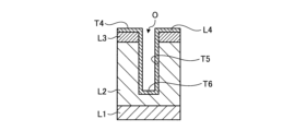
図6Aは、一実施形態に係るプラズマ処理が適用される処理対象基板の一例を示す図である。図6Aの処理対象基板Sは、下地層L1と、第1層L2と、第2層L3と、を有する。処理対象基板Sには開口部Oが形成されている。下地層L1の上に、CVD等の成膜方法を用いて第1層L2を形成した後、第1層L2をエッチングする際のマスクとなる第2層L3を形成する。次に、第2層L3の上からエッチングを行い開口部Oを形成する。開口部Oは側壁T5と底部T6とを有する。かかる処理により、図6Aの処理対象基板Sが形成される。図6Aの状態においては、開口部Oの底面(底部T6の面)は、第1層L2内に位置する。
<Example of pattern formed by plasma treatment>
FIG. 6A is a diagram showing an example of a substrate to be processed to which plasma processing according to one embodiment is applied. The substrate to be processed S in FIG. 6A has an underlying layer L1, a first layer L2, and a second layer L3. An opening O is formed in the substrate S to be processed. After forming the first layer L2 on the underlying layer L1 using a film forming method such as CVD, the second layer L3 is formed as a mask when etching the first layer L2. Next, an opening O is formed by etching from above the second layer L3. Opening O has sidewalls T5 and bottom T6. Through such processing, the substrate to be processed S shown in FIG. 6A is formed. In the state of FIG. 6A, the bottom surface of the opening O (the surface of the bottom T6) is located within the first layer L2.
ここで、第1層L2を下地層L1近傍までエッチングする必要があるとする。また、開口部Oの側壁T5へのダメージを与えずにエッチングを実行することが好ましいとする。また、下地層L1にはダメージを加えずに第1層L2のエッチングを実行することが好ましいとする。 Here, it is assumed that it is necessary to etch the first layer L2 to the vicinity of the underlying layer L1. It is also assumed that it is preferable to perform the etching without damaging the side walls T5 of the opening O. FIG. It is also assumed that it is preferable to etch the first layer L2 without damaging the underlying layer L1.
また、下地層L1と第1層L2とは異なる材料で形成されているとする。たとえば、下地層L1は二酸化シリコン(SiO2)で形成され、第1層L2はシリコン(Si)または窒化シリコン(SiN)等で形成されているとする。また、第2層L3はSiO2等で形成されているとする。 It is also assumed that the base layer L1 and the first layer L2 are made of different materials. For example, assume that the base layer L1 is made of silicon dioxide (SiO2), and the first layer L2 is made of silicon (Si), silicon nitride (SiN), or the like. It is also assumed that the second layer L3 is made of SiO2 or the like.
このとき、開口部Oの側壁T5に与えるダメージを抑制するためには、側壁T5上に保護層を形成することが考えられる。たとえば、図6Bに示すように、処理対象基板Sに対してALDを実行してSiO2の保護層L4を形成することができる。図6Bは、図6Aに示す処理対象基板Sに形成される保護層の例を示す図である。 At this time, in order to suppress the damage to the sidewall T5 of the opening O, it is conceivable to form a protective layer on the sidewall T5. For example, as shown in FIG. 6B, ALD can be performed on the substrate S to be processed to form a protective layer L4 of SiO2. FIG. 6B is a diagram showing an example of a protective layer formed on the substrate S to be processed shown in FIG. 6A.
しかし、図6Bに示すような保護層L4を形成した場合、以下のような問題が生じる。まず、保護層L4の材料はSiO2であるのに対して、第1層L2の材料はSiまたはSiNである。すると、底部T6をさらにエッチングするためには、まず、保護層L4の材料であるSiO2に適した条件でエッチングを行うことで保護層L4を除去した上で、第1層L2をエッチングすることになる。保護層L4を除去するための工程をブレークスルー工程とも呼ぶ。ブレークスルー工程(例えば、300mmウェハWに対して、CF4、200sccm、30mTorr、アンテナ300W、13MHz、100W)を実行する場合、底部T6の面から下地層L1の上面までの距離が短いと、保護層L4を除去するためのエッチングの影響で下地層L1がダメージを受ける可能性がある。また、保護層L4と第1層L2のエッチングの選択比の制御が困難な場合には、保護層L4をエッチングする際に下地層L1が一緒にエッチングされてしまう可能性がある。この場合、図6Cに示すように、下地層L1がダメージを受ける可能性がある。図6Cは、図6Bに示す処理対象基板Sの開口部Oにエッチングを施した場合について説明するための図である。 However, when the protective layer L4 as shown in FIG. 6B is formed, the following problems arise. First, the material of the protective layer L4 is SiO2, while the material of the first layer L2 is Si or SiN. Then, in order to further etch the bottom portion T6, first, the protective layer L4 is removed by etching under conditions suitable for SiO2, which is the material of the protective layer L4, and then the first layer L2 is etched. Become. A process for removing the protective layer L4 is also called a breakthrough process. When performing a breakthrough process (for example, CF4, 200 sccm, 30 mTorr, antenna 300 W, 13 MHz, 100 W for a 300 mm wafer W), if the distance from the surface of the bottom T6 to the upper surface of the underlying layer L1 is short, the protective layer Underlying layer L1 may be damaged by the etching for removing L4. Moreover, if it is difficult to control the etching selectivity between the protective layer L4 and the first layer L2, the base layer L1 may be etched together when the protective layer L4 is etched. In this case, as shown in FIG. 6C, the underlying layer L1 may be damaged. FIG. 6C is a diagram for explaining the case where the opening O of the substrate S to be processed shown in FIG. 6B is etched.
これに対して、図5に示す一実施形態に係るプラズマ処理においては、プラズマ処理装置100は、開口部Oが所定の条件を満足した、と判定した場合(図5、ステップS53、Yes)には、その時点でまずエッチングを停止する。そして、プラズマ処理装置100は、インヒビター層を形成した(図5、ステップS54)上で保護層を形成するためのALDサイクル(図5、ステップS55)を実行する。インヒビター層はたとえば、図2において説明したように、後続のALDサイクルにおけるインキュベーションタイムを発生させる層である。たとえば、インヒビター層とは、後続のALDサイクルにおいて前駆体ガスの吸着を阻害する材料で形成される層である。インヒビター層とは、たとえば、疎水性の表面を有する層である。またたとえば、インヒビター層とはフッ素(F)を含む層である。またたとえば、インヒビター層とは、フルオロカーボンを含むガスにより形成される層である。またたとえば、インヒビター層とは、水素を含まないガスにより形成される層である。
On the other hand, in the plasma processing according to the embodiment shown in FIG. 5, when the
図7Aは、図6Aに示す処理対象基板Sに対してインヒビター層L5を形成した場合の一例を示す図である。図6Aに示す開口部Oが形成された処理対象基板Sについて、開口部Oが所定の条件を満足した、と判定された場合に、インヒビター層L5の形成処理が実行される。ここで、開口部Oが満足すべき所定の条件とは、たとえば、開口部Oの深さが所定深さに達したことや、開口部Oの底部T6の面から下地層L1の上面までの距離が所定距離に達したこと、等である。所定の条件が満足されたか否かは、たとえば、処理開始から所定時間が経過したか否かに基づいて判定することができる。ここでは、開口部Oの底部T6の面から下地層L1の上面までの距離が所定距離に達した場合に、プラズマ処理装置100は、開口部Oは所定の条件を満足した、と判定する。所定距離は、その距離以下でブレークスルー工程を入れると下地層L1にダメージが入る可能性があると判断される距離である。たとえば所定距離は、20ナノメートル(nm)である。
FIG. 7A is a diagram showing an example of forming an inhibitor layer L5 on the substrate S to be processed shown in FIG. 6A. For the processing target substrate S having the opening O shown in FIG. 6A, when it is determined that the opening O satisfies a predetermined condition, the formation process of the inhibitor layer L5 is performed. Here, the predetermined condition to be satisfied by the opening O is, for example, that the depth of the opening O has reached a predetermined depth, or that the depth from the bottom T6 of the opening O to the upper surface of the underlying layer L1 For example, the distance has reached a predetermined distance. Whether or not a predetermined condition is satisfied can be determined, for example, based on whether or not a predetermined period of time has elapsed since the start of processing. Here, when the distance from the surface of the bottom T6 of the opening O to the upper surface of the underlying layer L1 reaches a predetermined distance, the
インヒビター層L5の形成は、たとえばCVDにより処理対象基板Sが有するパターンの所定部分にフルオロカーボンを堆積させて行う。たとえば、異方性CVDを使用することで概ね一方向にFCが堆積し、一方向と異なる方向にはFCが堆積しない。たとえば、処理対象基板Sの上表面に対して直交する方向にFCが堆積する一方、上表面と水平方向にはFCが堆積しない。図7Aの例では、頂部T4および底部T6にはインヒビター層L5が形成されているが、側壁T5上にはインヒビター層L5は形成されていない。 The inhibitor layer L5 is formed by depositing fluorocarbon on a predetermined portion of the pattern of the substrate S to be processed, for example, by CVD. For example, the use of anisotropic CVD results in FC deposition generally in one direction and no FC deposition in a direction other than one direction. For example, while FC is deposited in a direction orthogonal to the upper surface of the substrate S to be processed, FC is not deposited in a direction horizontal to the upper surface. In the example of FIG. 7A, the inhibitor layer L5 is formed on the top T4 and the bottom T6, but the inhibitor layer L5 is not formed on the sidewall T5.
次に、プラズマ処理装置100はALDサイクルを実行する(図5、ステップS55)。すなわち、プラズマ処理装置100は、インヒビター層L5が形成された処理対象基板Sを前駆体ガスXに晒して、インヒビター層L5が形成されていない部分に前駆体ガスXを吸着させる。たとえば、図7Aの例であれば、インヒビター層L5が形成されていない側壁T5上に前駆体ガスXが吸着する。さらに、プラズマ処理装置100は、処理対象基板Sを反応ガスに晒す。すると、側壁T5上に吸着した前駆体ガスXの原子と反応ガスの原子とが結合し、保護層L6が形成される。図7Bは、図7Aに示す処理対象基板Sのインヒビター層L5を利用して保護層L6を形成した場合の一例を示す図である。保護層L6は、インヒビター層L5が形成されなかった位置に形成される。図7Bの例では、開口部Oの側壁T5上に保護層L6が形成される。なお、図7Bの例は、インヒビター層L5が除去されてなくなるまでALDサイクルを繰り返し実行した後の状態である。
Next, the
次に、プラズマ処理装置100は、ALDの結果所定条件を満足した、と判定した場合(図5、ステップS56、Yes)、保護層L6が形成された処理対象基板Sの開口部Oをエッチングする(図5、ステップS57)。
Next, when the
図7Bに示す例の場合、図6Bに示す例と異なり、開口部Oの底部T6には保護層L6が形成されていない。このため、ステップS56の判定後に直ちに第1層L2を直接エッチングすることができる。このため、ブレークスルー工程を介在させることなく、第1層L2のエッチングに適した条件でエッチングを実行することができる。また、下地層L1と第1層L2との間で選択比が取れるようにエッチング条件を設定することができる。 In the example shown in FIG. 7B, unlike the example shown in FIG. 6B, the protective layer L6 is not formed on the bottom T6 of the opening O. As shown in FIG. Therefore, the first layer L2 can be directly etched immediately after the determination in step S56. Therefore, etching can be performed under conditions suitable for etching the first layer L2 without intervening a breakthrough step. Also, the etching conditions can be set so as to obtain a selectivity between the base layer L1 and the first layer L2.
図7Cは、図7Bに示す処理対象基板Sの開口部Oにエッチングを施した場合について説明するための図である。図7Bの処理対象基板Sに対してエッチングを行うことで、図7Cに示すように下地層L1近傍まで第1層L2をエッチングしても、下地層L1へのダメージを抑制することができる。また、エッチングの間、側壁T5は保護層L6によって保護されるため、側壁T5へのダメージ(ボーイング)もなくすことができる。 FIG. 7C is a diagram for explaining the case where the opening O of the substrate S to be processed shown in FIG. 7B is etched. By etching the substrate S to be processed in FIG. 7B, damage to the underlying layer L1 can be suppressed even if the first layer L2 is etched to the vicinity of the underlying layer L1 as shown in FIG. 7C. Moreover, since the side wall T5 is protected by the protective layer L6 during etching, damage (bowing) to the side wall T5 can also be eliminated.
<インヒビター層の形成位置>
図7A乃至図7Cに示す例では、インヒビター層L5を頂部T4および底部T6に形成するものとした。インヒビター層を形成する位置および膜厚分布は、プラズマCVDの条件(たとえば等方性か異方性か等)を変更することにより変更することができる。このため、上記実施形態のようにインヒビター層L5を頂部T4および底部T6に形成する場合は、プラズマCVDの条件を以下の条件等から適宜選択してインヒビター層L5を形成する。
<Position of formation of inhibitor layer>
In the example shown in FIGS. 7A to 7C, the inhibitor layer L5 is formed on the top portion T4 and the bottom portion T6. The position where the inhibitor layer is formed and the film thickness distribution can be changed by changing the plasma CVD conditions (for example, isotropic or anisotropic). Therefore, when the inhibitor layer L5 is formed on the top portion T4 and the bottom portion T6 as in the above embodiment, the plasma CVD conditions are appropriately selected from the following conditions and the like to form the inhibitor layer L5.
(ガス種)
たとえば、CVDにおいて用いるガス種を変更することにより、インヒビター層の形成位置および膜厚分布を調整することができる。インヒビター層をCVDで形成するガスとしては、C4F6ガスまたはC4F8ガスを用いることができる。C4F6ガスの付着係数はC4F8ガスの付着係数よりも大きい。よって、C4F6を用いると、インヒビター層はウエハWの表面側(低アスペクト領域)により多く形成される。一方、C4F8を用いるとインヒビター層は底部側(高アスペクト領域)により多く形成される。ここでは、低アスペクト領域とは、ウエハWの表面に相対的に近い領域を、高アスペクト領域とは、ウエハWの表面から相対的に遠い領域を指すものとする。このようにガス種によって付着係数が異なるので、ガス種を変更することによってインヒビター層の形成される位置を制御することができる。
(Gas type)
For example, by changing the type of gas used in CVD, the formation position and film thickness distribution of the inhibitor layer can be adjusted. As a gas for forming the inhibitor layer by CVD, C4F6 gas or C4F8 gas can be used. The sticking coefficient of C4F6 gas is higher than that of C4F8 gas. Therefore, when C4F6 is used, more of the inhibitor layer is formed on the surface side of the wafer W (low aspect region). On the other hand, when C4F8 is used, more of the inhibitor layer is formed on the bottom side (high aspect area). Here, the low-aspect region refers to a region relatively close to the surface of the wafer W, and the high-aspect region refers to a region relatively far from the wafer W surface. Since the adhesion coefficient differs depending on the gas species, the position where the inhibitor layer is formed can be controlled by changing the gas species.
(バイアス電力)
また、載置台110に印加されるバイアス高周波電源の電力を変更することにより、インヒビター層の形成位置および膜厚分布を調整することができる。たとえば、当該電力をオン・オフしてもよい。また、当該電力の値を高い値と低い値との間で変化させてもよい。当該電力の値を高くするとインヒビター層はウエハWの水平面(たとえば図6Aの頂部T4と底部T6)に厚く形成される。他方、インヒビター層はウエハWの垂直面(たとえば図6Aの側壁T5)に薄く形成される。当該電力の値を小さくすると、インヒビター層は上部側すなわちウエハW表面に相対的に近い位置により多く形成される。
(Bias power)
Further, by changing the power of the bias high-frequency power supply applied to the mounting table 110, the formation position and film thickness distribution of the inhibitor layer can be adjusted. For example, the power may be turned on and off. Also, the value of the power may be varied between a high value and a low value. When the power value is increased, the inhibitor layer is formed thicker on the horizontal surfaces of the wafer W (for example, the top portion T4 and the bottom portion T6 in FIG. 6A). On the other hand, the inhibitor layer is thinly formed on the vertical surface of the wafer W (eg sidewall T5 in FIG. 6A). When the value of the electric power is decreased, more of the inhibitor layer is formed on the upper side, that is, the position relatively close to the wafer W surface.
(ウエハの温度)
また、インヒビター層形成時のウエハWの温度を変更することで、インヒビター層の形成位置および膜厚分布を調整できる。ウエハWの温度が相対的に高くなると、インヒビター層は底部側(高アスペクト領域)により多く成膜される。ウエハWの温度が相対的に低くなると、インヒビター層はウエハWの表面側(低アスペクト領域)により多く形成される。
(wafer temperature)
Further, by changing the temperature of the wafer W during the formation of the inhibitor layer, the formation position and film thickness distribution of the inhibitor layer can be adjusted. When the temperature of the wafer W becomes relatively high, more of the inhibitor layer is formed on the bottom side (high aspect area). When the temperature of wafer W becomes relatively low, more of the inhibitor layer is formed on the surface side of wafer W (low aspect region).
(圧力)
また、インヒビター層形成時の処理室102内の圧力を変更することで、インヒビター層の形成位置および膜厚分布を調整できる。処理室102内の圧力を相対的に高くすると生成されるプラズマは等方的となる。等方的なプラズマによりウエハWの表面側(低アスペクト領域)により厚いインヒビター層が形成される。他方、処理室102内の圧力が相対的に低くなると生成されるプラズマは異方的となる。異方的なプラズマにより底部側(高アスペクト領域)により厚いインヒビター層が形成される。
(pressure)
Further, by changing the pressure in the
(プラズマ生成用の高周波電力)
また、プラズマCVDの際に用いるプラズマ励起用の高周波電力の値を変更することで、インヒビター層の形成位置および膜厚分布を調整できる。プラズマ励起用の高周波電力の値を変更することによって、プラズマの解離状態を変更することができる。従って、当該電力を変更することによって、プラズマCVDにおいて生成されるラジカル種またはラジカル比率が変更され、インヒビター層が成膜される際の付着係数が変更される。付着係数が大きくなるように高周波電力の値を変更すれば、インヒビター層はウエハWの表面側(低アスペクト領域)により多く形成される。また、付着係数が小さくなるように高周波電力の値を変更すれば、インヒビター層はウエハWの底部側(高アスペクト領域)により多く形成される。
(High frequency power for plasma generation)
Further, by changing the value of the high-frequency power for plasma excitation used in plasma CVD, the formation position and film thickness distribution of the inhibitor layer can be adjusted. By changing the value of the high frequency power for plasma excitation, the dissociation state of the plasma can be changed. Therefore, by changing the power, the radical species or the ratio of radicals generated in plasma CVD is changed, and the sticking coefficient when the inhibitor layer is formed is changed. If the value of the high-frequency power is changed so as to increase the sticking coefficient, more of the inhibitor layer is formed on the surface side of the wafer W (low aspect region). Also, if the value of the high-frequency power is changed so that the sticking coefficient becomes small, more of the inhibitor layer is formed on the bottom side of the wafer W (high-aspect region).
(イオンレスでのインヒビター層形成)
図7Aのインヒビター層L5は、頂部T4および底部T6に形成されている。しかし、パターンのアスペクト比が増加するとともにパターンの開口寸法が小さくなると、CVDによって底部T6にインヒビター層L5を形成する際に開口閉塞が生じる可能性がある。インヒビター層L5を形成するための処理ガスを底部T6まで送り込むためには、CVDの際のイオンエネルギーが高くなるよう処理条件を設定することが考えられる。しかし、イオンエネルギーを高く設定すると、インヒビター層L5を形成する際に、下地層L1にもダメージが生じる可能性がある。
(Inhibitor layer formation without ions)
Inhibitor layer L5 in FIG. 7A is formed on top T4 and bottom T6. However, as the aspect ratio of the pattern increases and the opening dimension of the pattern decreases, there is a possibility that opening blockage will occur when the inhibitor layer L5 is formed on the bottom T6 by CVD. In order to send the processing gas for forming the inhibitor layer L5 to the bottom T6, it is conceivable to set the processing conditions so that the ion energy during CVD becomes high. However, if the ion energy is set high, the underlying layer L1 may also be damaged when the inhibitor layer L5 is formed.
そこで、高アスペクト比のパターンの底部にインヒビター層を形成する場合には、イオンレスの処理またはイオンエネルギーを低く設定した処理条件での処理が好ましい。たとえば、毛管凝縮(capillary condensation)を利用した処理を採用することができる。毛管凝縮とは、毛管すなわち細孔内の飽和蒸気圧が平面の飽和蒸気圧よりも低くなる現象をいう。言い換えると、気体が臨界点以下で毛管と接したときに液体となって凝縮する現象である。毛管凝縮式により、毛管の半径が小さいほど毛管内の蒸気圧も小さくなり凝縮が生じやすくなることが知られている。これを、半導体パターンに当てはめると、パターンのアスペクト比が高くなるほど(毛管の半径が小さくなるほど)、当該パターン内の蒸気圧も小さくなり凝縮が生じやすくなると言える。この現象を利用して処理対象基板のパターンのうち開口が小さいパターンに優先的に処理ガスの液化および/または固体化を生じさせることができる。かかる手法は特に高アスペクト比のパターン底部にインヒビター層を形成するときに効果的である。 Therefore, in the case of forming an inhibitor layer on the bottom of a pattern with a high aspect ratio, ionless processing or processing under processing conditions in which ion energy is set low is preferable. For example, a process utilizing capillary condensation can be employed. Capillary condensation is a phenomenon in which the saturated vapor pressure in capillaries, ie pores, is lower than the saturated vapor pressure in the plane. In other words, it is a phenomenon in which gas becomes liquid and condenses when it comes into contact with the capillary below the critical point. According to the capillary condensation method, it is known that the smaller the radius of the capillary, the smaller the vapor pressure in the capillary and the more likely condensation occurs. If this is applied to a semiconductor pattern, it can be said that the higher the aspect ratio of the pattern (the smaller the radius of the capillary), the lower the vapor pressure in the pattern and the more likely condensation occurs. By utilizing this phenomenon, it is possible to preferentially liquefy and/or solidify the processing gas in patterns with small openings among the patterns of the substrate to be processed. Such a technique is particularly effective when forming an inhibitor layer on the bottom of a pattern with a high aspect ratio.
図8は、毛管凝縮を利用したインヒビター層の形成手法の一例について説明するための図である。図8の実験結果は以下の処理条件1で実験を行って得た。実験にはウエハ上にシリコン窒化膜が形成されたサンプルを用いた。シリコン窒化膜には予めアスペクト比3~5の凹部および平面部を形成した。実験には、処理室上方にプラズマ生成用の高周波HFを供給し、載置台にバイアス引き込み用の高周波LFを供給する誘導結合型プラズマ処理装置を用いた。
<処理条件1>
チャンバ内圧力:50mT(6.65Pa)
ガス種/流量:C4F6、300sccm
ステージ温度:-50℃
高周波HFのパワー:300W
高周波LFのパワー:0W
FIG. 8 is a diagram for explaining an example of a technique for forming an inhibitor layer using capillary condensation. The experimental results shown in FIG. 8 were obtained by conducting an experiment under
<
Chamber pressure: 50 mT (6.65 Pa)
Gas type/flow rate: C4F6, 300 sccm
Stage temperature: -50°C
High frequency HF power: 300W
High frequency LF power: 0W
図8中、(a)~(d)は各々、処理時間を2秒、4秒、7秒および10秒に設定して得られたパターンを示す。図8中、凹部A~G,平面部Hは深さが略同一である。凹部A,C,Eの開口寸法は略同一、凹部B,Dの開口寸法も略同一である。また、凹部Fは、凹部A~Eよりも開口寸法が小さい。凹部Gは、凹部Aよりも開口寸法が大きく、凹部Bよりも開口寸法が小さい。このため、各凹部のアスペクト比は、凹部B,D、凹部G、凹部A,C,E、凹部Fの順に高くなっている。 In FIG. 8, (a) to (d) show patterns obtained by setting the processing time to 2 seconds, 4 seconds, 7 seconds and 10 seconds, respectively. In FIG. 8, the concave portions A to G and the plane portion H have substantially the same depth. The opening dimensions of the recesses A, C and E are substantially the same, and the opening dimensions of the recesses B and D are also substantially the same. Further, the recess F has a smaller opening size than the recesses A to E. The recess G has a larger opening dimension than the recess A and a smaller opening dimension than the recess B. Therefore, the aspect ratio of each recess increases in the order of recesses B, D, recess G, recesses A, C, E, and recess F. FIG.
図8中、(a)において、凹部A,C,Eよりもアスペクト比が高い凹部Fは、凹部A,C,Eよりも早くCF膜で充填されている。また、CF膜は流動性有機膜として凹部F内に充填されるため、凹部Fの開口は閉塞されていない。 In FIG. 8A, the concave portion F having a higher aspect ratio than the concave portions A, C, and E is filled with the CF film earlier than the concave portions A, C, and E. In FIG. Further, since the CF film is filled in the concave portion F as a fluid organic film, the opening of the concave portion F is not blocked.
また、図8の(b)では、凹部B,DにはCF膜が堆積しておらず、凹部A,C,EにCF膜が充填し、凹部GにもCF膜が充填している。なお、(b)の状態では、平面部HにはCF膜はほとんど形成されていない。 Further, in FIG. 8B, the CF film is not deposited in the recesses B and D, the recesses A, C and E are filled with the CF film, and the recess G is also filled with the CF film. In the state of (b), almost no CF film is formed on the plane portion H. FIG.
図8の(c)では、平面部HにおいてもCF膜の堆積が認められる。図8の(d)では、凹部A~GはCF膜により概ね充填され、平面部Hもさらに多くのCF膜が堆積している。図8から分かるように、毛管凝縮を利用した手法では、高アスペクト比のパターンにおいて低アスペクト比のパターンよりも早くCF膜が充填される。言い換えれば、アスペクト比が高い凹部ほど成膜速度が速くなる。また、凹部の底面からCF膜が成長するように充填されている。このため、毛管凝縮を利用して処理時間を調整することで、下地層にダメージを与えずにCF膜を形成することができる。 In (c) of FIG. 8, the deposition of the CF film is recognized even on the plane portion H. As shown in FIG. In (d) of FIG. 8, the concave portions A to G are mostly filled with the CF film, and the planar portion H is also deposited with a larger amount of the CF film. As can be seen from FIG. 8, the capillary condensation approach fills the CF film faster in high aspect ratio patterns than in low aspect ratio patterns. In other words, the higher the aspect ratio of the recess, the faster the deposition rate. Also, the recess is filled so that the CF film grows from the bottom surface of the recess. Therefore, by adjusting the processing time using capillary condensation, the CF film can be formed without damaging the underlying layer.
図9Aは、毛管凝縮を利用してインヒビター層L5が形成された処理対象基板Sの一例を示す図である。図9Bは、図9Aに示す処理対象基板Sにアッシングを行った状態の一例を示す図である。図9Cは、図9Bに示す処理対象基板Sに保護層L6を形成した状態の一例を示す図である。 FIG. 9A is a diagram showing an example of the substrate S to be processed on which the inhibitor layer L5 is formed using capillary condensation. FIG. 9B is a diagram showing an example of a state where the substrate S to be processed shown in FIG. 9A is ashed. FIG. 9C is a diagram showing an example of a state in which a protective layer L6 is formed on the substrate S to be processed shown in FIG. 9B.
まず、処理対象基板Sに対して、毛管凝縮を利用してインヒビター層L5を形成する。インヒビター層L5は極低温かつイオンレスで形成されるため、下地層L1および第1層L2へのダメージが抑制できる。その後、アッシングを行ってインヒビター層L5の膜厚を調整する。アッシングは省略してもよい。その後、ALDにより保護層L6を形成する。このように、毛管凝縮を利用してインヒビター層L5を形成すれば、開口閉塞や下地層へのダメージを防止することができる。 First, the inhibitor layer L5 is formed on the substrate S to be processed using capillary condensation. Since the inhibitor layer L5 is formed at an extremely low temperature and without ions, damage to the base layer L1 and the first layer L2 can be suppressed. Thereafter, ashing is performed to adjust the film thickness of the inhibitor layer L5. Ashing may be omitted. After that, a protective layer L6 is formed by ALD. By forming the inhibitor layer L5 by utilizing capillary condensation in this way, it is possible to prevent opening clogging and damage to the underlying layer.
<毛管凝縮を利用した処理の温度依存性および圧力依存性>
なお、毛管凝縮を利用してインヒビター層をパターン底部から積み上げるように形成する場合、形成されるインヒビター層は温度依存性および圧力依存性を有する。このため、処理時の温度および圧力を制御して処理を実行する。たとえば、載置台110の温度を極低温領域たとえば-70℃~-20℃程度に制御して処理を実行する。また、処理室102内の圧力をたとえば50mT以上に設定する。また、Ei<10eV以下の低イオン量となるように処理条件を調整する。たとえば、載置台110の温度を-20℃以下、処理室102内の圧力を50mT以上に設定することが好ましい。
<Temperature Dependence and Pressure Dependence of Treatment Using Capillary Condensation>
When the inhibitor layer is formed so as to build up from the bottom of the pattern using capillary condensation, the formed inhibitor layer has temperature dependency and pressure dependency. For this reason, the temperature and pressure during processing are controlled to perform the processing. For example, the temperature of the mounting table 110 is controlled to an extremely low temperature range, for example, about -70°C to -20°C, and the process is executed. Also, the pressure inside the
例として、C4F6ガス流量を300sccm、処理室102内の圧力を100mTに設定して、載置台110の温度を変化させながらインヒビター層を形成した。この場合、-10℃、-20℃では、等方向に膜が形成されて開口が狭まりボイドが発生した。ボイドとは、開口が塞がることで凹部の内部に形成される空洞である。他方、-30℃、-50℃では、パターン底部から積み上げるようにインヒビター層が形成され、ボイドの発生は観察されなかった。
As an example, the C4F6 gas flow rate was set to 300 sccm, the pressure inside the
他方、C4F6ガス流量を300sccm、処理室102内の圧力を50mTとした場合、-10℃ではボイドが発生して等方向に成膜された。他方、-20℃、-30℃、-50℃では、パターン底部から積み上げるようにインヒビター層が形成された。
On the other hand, when the C4F6 gas flow rate was 300 sccm and the pressure in the
なお、C4F6ガス流量を125sccm、処理室102内の圧力を50mTとした場合には、-10℃および-20℃でボイドが発生して等方向に成膜され、-30℃ではパターン底部から積み上げるようにインヒビター層が形成されている。
When the C4F6 gas flow rate is 125 sccm and the pressure in the
また、IPA(イソプロピルアルコール:C3H8O)ガスを75sccm、処理室102内の圧力を50mTとした場合、-10℃および-30℃の場合にボイドが発生して等方向の成膜が行われ、-40℃および-50℃の場合にはボトムアップで流動性の膜が形成された。
Further, when the IPA (isopropyl alcohol: C3H8O) gas is 75 sccm and the pressure in the
このように、ボトムアップでパターン底部にインヒビター層を形成するための処理条件は、ガス種、圧力およびガス流量によって変化する。ただし、少なくともC4F6ガスの流量を300sccmとした場合は、載置台110の温度を-20℃以下の極低温に維持し、処理室102内を50mT以上の圧力に維持することで、ボトムアップ成膜が実現できる。
Thus, the processing conditions for bottom-up formation of the inhibitor layer on the bottom of the pattern vary depending on the gas species, pressure and gas flow rate. However, when the flow rate of the C4F6 gas is at least 300 sccm, the temperature of the mounting table 110 is maintained at an extremely low temperature of −20° C. or lower, and the pressure in the
また、ガス種については、C4F6ガスの蒸気圧曲線が示す温度以上の温度で蒸気圧になるガスを用いる。たとえば、C4F8、C4F6、IPA(イソプロピルアルコール)は、C4F8ガスの蒸気圧曲線が示す温度と同じまたはそれ以上の温度で蒸気圧となる。かかるガスを用いてウエハW上に成膜する。なお、成膜時にはプラズマを生成しても生成しなくてもよい。なお、上記ガスは炭素含有ガスであってもよい。 As for the gas type, a gas whose vapor pressure is equal to or higher than the temperature indicated by the vapor pressure curve of C4F6 gas is used. For example, C4F8, C4F6, and IPA (isopropyl alcohol) have vapor pressures at or above the temperature indicated by the vapor pressure curve for C4F8 gas. A film is formed on the wafer W using such gas. Note that plasma may or may not be generated during film formation. Note that the gas may be a carbon-containing gas.
このように、処理条件や使用するガス種を変更することによって、所望の位置に所望の膜厚分布のインヒビター層を形成してプラズマ処理を実行することができる。また、下地層へのダメージを抑制しつつパターンを形成することができる。 In this way, by changing the processing conditions and the type of gas used, it is possible to form an inhibitor layer having a desired film thickness distribution at a desired position and perform plasma processing. Moreover, the pattern can be formed while suppressing damage to the underlying layer.
<実施形態の効果>
上記のように、実施形態に係るプラズマ処理方法は、開口部形成工程(ステップS52)と、第1膜形成工程(ステップS54)と、第2膜形成工程(ステップS55)と、エッチング工程(ステップS57)と、を含む。プラズマ処理装置100は、開口部形成工程において、下地層L1と下地層L1上に形成される第1層L2とを含む処理対象基板Sに対してエッチングを施すことにより、第1層S2に開口部Oを形成する。さらに、プラズマ処理装置100は、開口部Oが所定条件を満足したと判定した場合、第1膜形成工程を実行する。第1膜形成工程においては、プラズマ処理装置100は、化学気相成長により、開口部Oの底面T6にインヒビターを形成することで所定のガス種が吸着しない第1の膜(インヒビター層L5)を形成する。プラズマ処理装置100は、第1の膜の形成後、第2膜形成工程において、所定のガス種を前駆体ガスとする原子層堆積により開口部Oの側壁T5に第2の膜(保護層L4)を形成する。そして、プラズマ処理装置100は、エッチング工程において、開口部Oにエッチングを施す。このため、開口部Oの側壁T5は第2の膜によって保護されエッチングによるダメージを受けない。また、開口部Oの底部T6において、ブレークスルー工程が不要となるため、プラズマ処理装置100は、下地層L1にダメージを与えることなく高精度に開口をエッチングすることができる。このように、実施形態に係るプラズマ処理方法は、プラズマ処理においてパターンに与えるダメージを低減することができる。
<Effects of Embodiment>
As described above, the plasma processing method according to the embodiment includes the opening forming step (step S52), the first film forming step (step S54), the second film forming step (step S55), and the etching step (step S57) and. In the opening forming step, the
また、上記実施形態のプラズマ処理方法は、開口部Oの底面T6と下地層L1の表面との間の距離が所定距離以下か否かを判定する判定工程(図5、ステップS53)をさらに含む。そして、プラズマ処理方法は、第1膜形成工程(図5、ステップS54)および第2膜形成工程(図5、ステップS55)は、距離が所定距離以下であると判定した場合(図5、ステップS53、Yes)に実行する。 Moreover, the plasma processing method of the above embodiment further includes a determination step (FIG. 5, step S53) of determining whether or not the distance between the bottom surface T6 of the opening O and the surface of the underlying layer L1 is equal to or less than a predetermined distance. . In the plasma processing method, the first film forming step (FIG. 5, step S54) and the second film forming step (FIG. 5, step S55) are performed when it is determined that the distance is equal to or less than the predetermined distance (FIG. 5, step S53, Yes).
また、上記実施形態のプラズマ処理方法の判定工程における所定距離は例えば、20ナノメートルである。第1膜形成工程および第2膜形成工程の実行タイミングを、底部T6と下地層L1の表面との距離が20ナノメートル以下となったときとすることで、プラズマ処理装置100は、ダメージから保護したい位置に保護層を形成することができる。また、プラズマ処理装置100は、底部T6と下地層L1とが近くなってから第1層L2のエッチング条件を適切に設定することができる。
Moreover, the predetermined distance in the determination step of the plasma processing method of the above embodiment is, for example, 20 nanometers. By setting the execution timing of the first film forming step and the second film forming step to when the distance between the bottom portion T6 and the surface of the underlying layer L1 becomes 20 nm or less, the
また、上記実施形態のプラズマ処理方法の第2膜形成工程において、ALDサイクルは所定回数繰り返し実行する。このため本実施形態によれば、所望の厚みの第2の膜を成膜して後続のエッチングによるダメージを低減することができる。 In addition, in the second film formation step of the plasma processing method of the above embodiment, the ALD cycle is repeatedly performed a predetermined number of times. Therefore, according to this embodiment, it is possible to form the second film with a desired thickness and reduce damage caused by subsequent etching.
また、上記実施形態のプラズマ処理方法の各工程は、同一チャンバ内で実行する。このため本実施形態によれば、工程ごとに処理対象基板をチャンバから移動させて処理を行う等の手間を省くことができる。 Further, each step of the plasma processing method of the above embodiment is performed in the same chamber. Therefore, according to this embodiment, it is possible to save the trouble of moving the substrate to be processed from the chamber for each process.
また、上記実施形態のプラズマ処理方法において、各工程は、下地層L1と第1層L2とが異なる材料で構成される処理対象基板Sに対して実行する。このため本実施形態によれば、通常ブレークスルー工程が必要となる処理対象基板Sについても、ブレークスルー工程の手間を省くとともに、処理対象基板Sへのダメージを低減することができる。 Further, in the plasma processing method of the above embodiment, each step is performed on the substrate S to be processed in which the base layer L1 and the first layer L2 are made of different materials. Therefore, according to the present embodiment, even for the substrate S to be processed, which normally requires a breakthrough step, it is possible to save the trouble of the breakthrough step and reduce the damage to the substrate S to be processed.
また、上記実施形態のプラズマ処理方法の第2膜形成工程において、第2の膜L6を第1層L2とは異なる材料で形成する。このため本実施形態によれば、第1層L2のエッチング時に、第2の膜L6により保護される部分にダメージを与えないよう選択比を設定して処理を実行することができる。 Further, in the second film forming step of the plasma processing method of the above embodiment, the second film L6 is formed of a material different from that of the first layer L2. For this reason, according to the present embodiment, when etching the first layer L2, it is possible to set the selectivity so as not to damage the portion protected by the second film L6.
また、上記実施形態のプラズマ処理方法において、各工程は、下地層L1がSiO2、第1層L2がSiNまたはSiで形成される前記処理対象基板Sに対して実行し、第2膜形成工程は、第2の膜L6をSiO2膜で形成する。また、上記実施形態のプラズマ処理方法において、各工程は、下地層L1がSi、第1層L2がSiO2で形成される処理対象基板Sに対して実行し、第2膜形成工程は、第2の膜L6をSiNで形成する。このため本実施形態によれば、広く利用されている半導体装置材料を対象として、パターンに与えるダメージを低減することができる。 Further, in the plasma processing method of the above embodiment, each step is performed on the substrate S to be processed in which the underlying layer L1 is formed of SiO2 and the first layer L2 is formed of SiN or Si, and the second film forming step is , the second film L6 is formed of an SiO2 film. Further, in the plasma processing method of the above embodiment, each step is performed on the substrate S to be processed in which the base layer L1 is Si and the first layer L2 is SiO2, and the second film forming step is performed on the second film forming step. is formed of SiN. Therefore, according to the present embodiment, it is possible to reduce the damage to the pattern of widely used semiconductor device materials.
<変形例>
ところで、上記実施形態では、処理対象基板Sが備える開口部Oの底部T6の面と下地層L1の表面までの距離が20ナノメートル以下になると、インヒビター層L5の形成を開始するものとした。これに限らず、たとえば下地層L1にダメージが発生したと判定した場合に、インヒビター層L5の形成を開始するように、プラズマ処理装置100を形成することができる。
<Modification>
By the way, in the above embodiment, the formation of the inhibitor layer L5 is started when the distance between the surface of the bottom T6 of the opening O provided in the substrate S to be processed and the surface of the underlying layer L1 becomes 20 nanometers or less. For example, the
図10Aは、変形例にかかるプラズマ処理が適用される処理対象基板の一例を示す図である。図10Aの処理対象基板S1は、図6Aの処理対象基板Sと同様に、下地層L1、第1層L2、第2層L3を有する。ただし、処理対象基板S1においては、第1層L2に形成された開口部O1の底面T9は、下地層L1に達している。また、下地層L1に形成された開口部O1の底面T9はエッチングにより酸化したダメージ層L7となっている。 FIG. 10A is a diagram illustrating an example of a substrate to be processed to which plasma processing according to a modification is applied; The processing target substrate S1 in FIG. 10A has a foundation layer L1, a first layer L2, and a second layer L3, like the processing target substrate S in FIG. 6A. However, in the processing target substrate S1, the bottom surface T9 of the opening O1 formed in the first layer L2 reaches the underlying layer L1. Further, the bottom surface T9 of the opening O1 formed in the underlying layer L1 is a damage layer L7 oxidized by etching.
変形例に係るプラズマ処理の流れは、図5に示す実施形態に係るプラズマ処理の流れと同様である。ただし、変形例においては、ステップS53における所定条件は、下地層L1内に位置する開口部O1の底部T9にダメージ層(酸化層)L7が形成されたこと、である。なお、ダメージ層L7が形成されたか否かの判定は、たとえば、プラズマの発光具合やエッチングの処理時間に基づいて行うことができる。たとえば、エッチングにより開口部O1の底部T9が下地層L1に達する時間を、ステップS52において実行するエッチングの処理時間としてプラズマ処理装置100の記憶部220に設定する。そして、プラズマ処理装置100は、エッチングの処理時間が終了した場合に、ステップS53の所定条件が満足されたと判定する。
The flow of plasma processing according to the modification is the same as the flow of plasma processing according to the embodiment shown in FIG. However, in the modified example, the predetermined condition in step S53 is that a damaged layer (oxidized layer) L7 is formed at the bottom T9 of the opening O1 located in the base layer L1. Whether or not the damaged layer L7 has been formed can be determined based on, for example, the degree of plasma emission and the etching processing time. For example, the time for the bottom T9 of the opening O1 to reach the base layer L1 by etching is set in the
変形例に係るプラズマ処理においては、開口部O1を形成するためのエッチング(ステップS52)の結果、下地層L1内に位置する開口部O1の底部T9にダメージ層L7が形成されたと判定された場合(ステップ53、Yes)に、インヒビター層L5を形成する。インヒビター層L5の形成とその後のALDの処理の流れは、実施形態にかかるプラズマ処理と同様である。変形例の場合もインヒビター層L5は、処理対象基板S1の頂部T7と底部T9にCVDによって形成される。その後、インヒビター層L5が形成されていない側壁T8上に保護層L6が形成される(図10B参照)。図10Bは、図10Aに示す処理対象基板Sに対して変形例に係るプラズマ処理により保護層を形成した場合の一例を示す図である。そして、保護層L6の上からダメージ層L7を除去するための処理が実行される。たとえば、化学的酸化物除去(Chemical Oxide Removal: COR)等のエッチングを用いてダメージ層L7を除去する。CORにおいては、HFガス、NF3ガス、NH3ガス等を使用することができる。また、フッ酸などを用いて湿式除去することができる。これによってダメージ層L7除去によりさらにダメージが拡大することを抑制する(図10C参照)。図10Cは、図10Bに示す処理対象基板から変形例にかかるプラズマ処理によりダメージ層を除去した場合の一例を示す図である。 In the plasma processing according to the modification, when it is determined that the damaged layer L7 is formed at the bottom T9 of the opening O1 located in the underlying layer L1 as a result of the etching (step S52) for forming the opening O1. In (step 53, Yes), an inhibitor layer L5 is formed. The flow of the formation of the inhibitor layer L5 and the subsequent ALD processing are the same as those of the plasma processing according to the embodiment. In the case of the modification, the inhibitor layer L5 is also formed by CVD on the top portion T7 and the bottom portion T9 of the substrate S1 to be processed. After that, a protective layer L6 is formed on the sidewall T8 where the inhibitor layer L5 is not formed (see FIG. 10B). FIG. 10B is a diagram showing an example of a case where a protective layer is formed on the processing target substrate S shown in FIG. 10A by plasma processing according to the modification. Then, a process is performed to remove the damaged layer L7 from above the protective layer L6. For example, an etch such as Chemical Oxide Removal (COR) is used to remove the damaged layer L7. HF gas, NF3 gas, NH3 gas, etc. can be used in COR. In addition, wet removal can be performed using hydrofluoric acid or the like. This suppresses the further expansion of the damage due to the removal of the damaged layer L7 (see FIG. 10C). FIG. 10C is a diagram showing an example of a case where a damaged layer is removed from the substrate to be processed shown in FIG. 10B by plasma processing according to the modification.
なお、図5に示すフローは一例であって、実施形態に係るプラズマ処理は他の工程を含んでもよい。また、ステップS53およびS56における所定条件の内容に応じて、図示したものとは異なる処理工程や処理順序を採用してもよい。 Note that the flow shown in FIG. 5 is an example, and the plasma processing according to the embodiment may include other steps. Also, depending on the contents of the predetermined conditions in steps S53 and S56, processing steps and processing order different from those illustrated may be adopted.
<変形例の効果>
上記変形例に係るプラズマ処理方法は、開口部形成工程(ステップS52)と、第1膜形成工程(ステップS54)と、第2膜形成工程(ステップS55)と、エッチング工程(ステップS57)と、を含む。プラズマ処理装置100は、開口部形成工程において、下地層L1と下地層L1上に形成される第1層L2とを含む処理対象基板S1に対してエッチングを施すことにより、第1層S2に開口部O1を形成する。さらに、プラズマ処理装置100は、第1膜形成工程において、開口部O1が所定条件を満足したと判定した場合、化学気相成長により、所定のガス種が吸着しない第1の膜(インヒビター層L5)を形成する。プラズマ処理装置100は、第1の膜を、開口部O1の底面T9にインヒビターを形成することで形成する。プラズマ処理装置100は、第1の膜の形成後、第2膜形成工程において、所定のガス種を前駆体ガスとする原子層堆積により開口部O1の側壁T8に第2の膜(保護層L6)を形成する。そして、プラズマ処理装置100は、エッチング工程において、開口部O1にエッチングを施す。プラズマ処理装置100は、エッチング工程が終了すると(ダメージ層L7が形成されたものとして)第1膜形成工程および第2膜形成工程を実行する。そして、プラズマ処理装置100は、エッチング工程においてダメージ層L7を除去する。このため本変形例によれば、処理過程において不所望のダメージ層L7が形成された場合であっても、他の部分にダメージを与えることなく、当該ダメージ層L7を除去することができる。
<Effect of modification>
The plasma processing method according to the modification includes an opening forming step (step S52), a first film forming step (step S54), a second film forming step (step S55), an etching step (step S57), including. In the opening forming step, the
なお、上記説明においては、下地層L1、第1層L2、第2の膜L6それぞれの材料の組み合わせ例の一つとして、下地層SiO2,第1層SiNまたはSi,第2の膜SiO2という組み合わせを提示した。また、他の組み合わせ例として、下地層Si、第1層SiO2、第2の膜SiNという組み合わせを提示した。ただし、この組み合わせに限らず、他の材料で構成される処理対象基板に本実施形態および変形例のプラズマ処理を適用することができる。 In the above description, the combination of the underlying layer SiO2, the first layer SiN or Si, and the second film SiO2 is one example of the combination of materials for the underlying layer L1, the first layer L2, and the second film L6. presented. Further, as another combination example, a combination of the underlying layer Si, the first layer SiO2, and the second film SiN was presented. However, the plasma processing of the present embodiment and modifications can be applied to substrates to be processed made of other materials without being limited to this combination.
今回開示された実施形態は全ての点で例示であって制限的なものではないと考えられるべきである。上記の実施形態は、添付の請求の範囲およびその趣旨を逸脱することなく、様々な形態で省略、置換、変更されてもよい。 It should be considered that the embodiments disclosed this time are illustrative in all respects and not restrictive. The above-described embodiments may be omitted, substituted or modified in various ways without departing from the scope and spirit of the appended claims.
100 プラズマ処理装置
102 処理室
110 載置台
L1 下地層
L2 第1層
L3 第2層
L4 保護層
L5 インヒビター層(第1の膜)
L6 保護層(第2の膜)
L7 ダメージ層
O,O1 開口部
S,S1 処理対象基板
T4,T7 頂部
T5,T8 側壁
T6,T9 底部
W ウエハ
100
L6 protective layer (second film)
L7 damaged layers O, O1 openings S, S1 substrates to be processed T4, T7 tops T5, T8 sidewalls T6, T9 bottoms W wafer
Claims (17)
(b)前記凹部が所定条件を満足したと判定した場合、前記凹部の底面に所定のガス種が吸着しない第1の膜を形成する工程と、
(c)前記工程(b)の後、前記所定のガス種を用いて前記凹部の側壁に第2の膜を形成する工程と、
(d)前記凹部を介して前記基板にエッチングを施す工程と、
を含むプラズマ処理方法。 (a) forming recesses in the first layer by etching a substrate including an underlying layer and a first layer formed on the underlying layer;
(b) forming a first film that does not adsorb a predetermined gas species on the bottom surface of the recess when it is determined that the recess satisfies a predetermined condition;
(c) after the step (b) , forming a second film on the side wall of the recess using the predetermined gas species;
(d) etching the substrate through the recess ;
A plasma processing method comprising:
(c1)前記基板を前記所定のガス種を含む前駆体ガスに晒し、前記前駆体ガスを前記凹部の側壁に吸着させる工程と、(c1) exposing the substrate to a precursor gas containing the predetermined gas species to cause the precursor gas to be adsorbed on the side wall of the recess;
(c2)前記基板を反応ガスから生成されたプラズマに晒し、前記前駆体ガス及び前記反応ガスから前記第2の膜を形成する工程と、(c2) exposing the substrate to a plasma generated from a reactive gas to form the second film from the precursor gas and the reactive gas;
を含む、請求項1または2に記載のプラズマ処理方法。 The plasma processing method according to claim 1 or 2, comprising:
前記工程(b)および(c)は、前記距離が前記所定距離以下であると判定した場合に実行する、請求項1から4のいずれか1項に記載のプラズマ処理方法。 (e) further comprising determining whether the distance between the bottom surface of the recess and the surface of the underlying layer is equal to or less than a predetermined distance;
5. The plasma processing method according to claim 1, wherein said steps (b) and (c) are performed when said distance is equal to or less than said predetermined distance.
前記工程(d)は、前記ダメージ層を除去する、請求項1から6のいずれか1項に記載のプラズマ処理方法。 The steps (b) and (c) are performed when it is determined that a damaged layer has been formed,
7. The plasma processing method according to claim 1, wherein said step (d) removes said damaged layer.
前記工程(c)は、前記第2の膜をSiO2膜で形成する、請求項1から10のいずれか1項に記載のプラズマ処理方法。 Each step is performed on the substrate in which the base layer is SiO2 and the first layer is SiN or Si,
11. The plasma processing method according to claim 1, wherein said step (c) forms said second film with a SiO2 film.
前記工程(c)は、前記第2の膜をSiNで形成する、請求項1から10のいずれか1項に記載のプラズマ処理方法。 Each step is performed on the substrate in which the base layer is Si and the first layer is SiO,
11. The plasma processing method according to claim 1, wherein said step (c) forms said second film of SiN.
前記所定のガス種はシリコンを含み、 the predetermined gas species includes silicon;
前記反応ガスは酸素又は窒素を含む、請求項3に記載のプラズマ処理方法。 4. The plasma processing method of claim 3, wherein the reactive gas contains oxygen or nitrogen.
(b)毛管凝縮を利用して前記凹部の底面にインヒビターにより所定のガス種が吸着しない第1の膜を形成する工程と、(b) using capillary condensation to form a first film on the bottom surface of the recess with an inhibitor that does not adsorb a predetermined gas species;
(c)前記工程(b)の後、前記所定のガス種を用いて前記凹部の側壁に第2の膜を形成する工程と、(c) after the step (b), forming a second film on the side wall of the recess using the predetermined gas species;
(d)前記凹部を介して前記基板をエッチングする工程と、(d) etching the substrate through the recess;
を含む、プラズマ処理方法。A plasma processing method, comprising:
前記プログラムの実行を制御する制御部と、
を備えるプラズマ処理装置であって、
前記制御部は、前記プログラムを実行することにより、
(a)下地層と下地層上に形成される第1層とを含む基板に対してエッチングを施すことにより、前記第1層に凹部を形成する工程と、
(b)前記凹部が所定条件を満足したと判定した場合、化学気相成長により、前記凹部の底面にインヒビターにより所定のガス種が吸着しない第1の膜を形成する工程と、
(c)前記工程(b)の後、前記所定のガス種を用いて前記凹部の側壁に第2の膜を形成する工程と、
(d)前記凹部を介して前記基板にエッチングを施す工程と
を実行させる、プラズマ処理装置。 a storage unit that stores a predetermined program;
a control unit that controls execution of the program;
A plasma processing apparatus comprising
By executing the program, the control unit
(a) forming recesses in the first layer by etching a substrate including an underlying layer and a first layer formed on the underlying layer;
(b) forming a first film on the bottom surface of the recess by chemical vapor deposition that does not adsorb a predetermined gas species by means of an inhibitor when it is determined that the recess satisfies a predetermined condition;
(c) after the step (b) , forming a second film on the side wall of the recess using the predetermined gas species;
(d) a plasma processing apparatus for performing the step of etching the substrate through the recess .
前記チャンバ内に配置される載置台と、 a mounting table arranged in the chamber;
制御部と control unit and
を備え、with
前記制御部は、 The control unit
(a)下地層と、前記下地層上の第1層とを含む基板を前記載置台上に配置する工程と、(a) disposing a substrate including an underlying layer and a first layer on the underlying layer on the mounting table;
(b)前記第1層をエッチングして、前記第1層に凹部を形成する工程と、(b) etching the first layer to form a recess in the first layer;
(c)前記凹部が所定の条件を満たすかどうかを判定する工程と、(c) determining whether the recess satisfies a predetermined condition;
(d)前記凹部が前記所定の条件を満たすと判定した場合に、インヒビターにより前記凹部の底部に所定のガス種が吸着しない第1の膜を形成する工程と、(d) forming a first film that does not adsorb a predetermined gas species on the bottom of the recess with an inhibitor when it is determined that the recess satisfies the predetermined condition;
(e)前記凹部の前記底部に、前記第1の膜に所定のガス種を吸着させることなく、前記所定のガス種によって前記凹部の側壁に、前記第1の膜と異なる第2の膜を形成する工程と、(e) forming a second film different from the first film on the side wall of the recess by using the predetermined gas species on the bottom of the recess without allowing the first film to adsorb the predetermined gas species; forming;
(f)前記凹部を介して前記第1層をエッチングする工程と、(f) etching the first layer through the recess;
を含む処理を実行するように構成されている、プラズマ処理装置。 A plasma processing apparatus configured to perform a process comprising:
Priority Applications (5)
| Application Number | Priority Date | Filing Date | Title |
|---|---|---|---|
| CN201910660252.XA CN110783187B (en) | 2018-07-25 | 2019-07-22 | Plasma processing method and plasma processing apparatus |
| TW108125906A TWI841579B (en) | 2018-07-25 | 2019-07-23 | Plasma processing method and plasma processing apparatus |
| US16/521,080 US11239090B2 (en) | 2018-07-25 | 2019-07-24 | Plasma processing method and plasma processing apparatus |
| KR1020190089863A KR20200011898A (en) | 2018-07-25 | 2019-07-24 | Plasma processing method and plasma processing apparatus |
| US17/560,228 US20220115241A1 (en) | 2018-07-25 | 2021-12-22 | Plasma processing method and plasma processing apparatus |
Applications Claiming Priority (2)
| Application Number | Priority Date | Filing Date | Title |
|---|---|---|---|
| JP2018139450 | 2018-07-25 | ||
| JP2018139450 | 2018-07-25 |
Publications (3)
| Publication Number | Publication Date |
|---|---|
| JP2020025078A JP2020025078A (en) | 2020-02-13 |
| JP2020025078A5 JP2020025078A5 (en) | 2022-05-31 |
| JP7257883B2 true JP7257883B2 (en) | 2023-04-14 |
Family
ID=69619505
Family Applications (1)
| Application Number | Title | Priority Date | Filing Date |
|---|---|---|---|
| JP2019097691A Active JP7257883B2 (en) | 2018-07-25 | 2019-05-24 | Plasma processing method and plasma processing apparatus |
Country Status (1)
| Country | Link |
|---|---|
| JP (1) | JP7257883B2 (en) |
Families Citing this family (1)
| Publication number | Priority date | Publication date | Assignee | Title |
|---|---|---|---|---|
| JP2023118554A (en) * | 2022-02-15 | 2023-08-25 | 東京エレクトロン株式会社 | Method for forming silicon nitride film and film forming apparatus |
Citations (8)
| Publication number | Priority date | Publication date | Assignee | Title |
|---|---|---|---|---|
| JP2005213632A (en) | 2004-02-02 | 2005-08-11 | Nec Electronics Corp | Deposition method |
| JP2008198659A (en) | 2007-02-08 | 2008-08-28 | Tokyo Electron Ltd | Plasma etching method |
| JP2008305921A (en) | 2007-06-06 | 2008-12-18 | Panasonic Corp | Semiconductor device and manufacturing method therefor |
| JP2011054742A (en) | 2009-09-01 | 2011-03-17 | Tokyo Electron Ltd | Film formation apparatus, and film formation method |
| JP2014017438A (en) | 2012-07-11 | 2014-01-30 | Tokyo Electron Ltd | Pattern formation method and substrate processing system |
| JP2016181630A (en) | 2015-03-24 | 2016-10-13 | 株式会社東芝 | Pattern forming method |
| JP2017005013A (en) | 2015-06-05 | 2017-01-05 | 東京エレクトロン株式会社 | Semiconductor device manufacturing method |
| JP2018037453A (en) | 2016-08-29 | 2018-03-08 | 東京エレクトロン株式会社 | Method for processing workpiece |
Family Cites Families (1)
| Publication number | Priority date | Publication date | Assignee | Title |
|---|---|---|---|---|
| JPH1041389A (en) * | 1996-07-24 | 1998-02-13 | Sony Corp | Manufacture of semiconductor device |
-
2019
- 2019-05-24 JP JP2019097691A patent/JP7257883B2/en active Active
Patent Citations (8)
| Publication number | Priority date | Publication date | Assignee | Title |
|---|---|---|---|---|
| JP2005213632A (en) | 2004-02-02 | 2005-08-11 | Nec Electronics Corp | Deposition method |
| JP2008198659A (en) | 2007-02-08 | 2008-08-28 | Tokyo Electron Ltd | Plasma etching method |
| JP2008305921A (en) | 2007-06-06 | 2008-12-18 | Panasonic Corp | Semiconductor device and manufacturing method therefor |
| JP2011054742A (en) | 2009-09-01 | 2011-03-17 | Tokyo Electron Ltd | Film formation apparatus, and film formation method |
| JP2014017438A (en) | 2012-07-11 | 2014-01-30 | Tokyo Electron Ltd | Pattern formation method and substrate processing system |
| JP2016181630A (en) | 2015-03-24 | 2016-10-13 | 株式会社東芝 | Pattern forming method |
| JP2017005013A (en) | 2015-06-05 | 2017-01-05 | 東京エレクトロン株式会社 | Semiconductor device manufacturing method |
| JP2018037453A (en) | 2016-08-29 | 2018-03-08 | 東京エレクトロン株式会社 | Method for processing workpiece |
Also Published As
| Publication number | Publication date |
|---|---|
| JP2020025078A (en) | 2020-02-13 |
| TW202011481A (en) | 2020-03-16 |
Similar Documents
| Publication | Publication Date | Title |
|---|---|---|
| CN112593212B (en) | Method for forming topologically selective silicon oxide film by cyclic plasma enhanced deposition process | |
| US11380551B2 (en) | Method of processing target object | |
| JP6373150B2 (en) | Substrate processing system and substrate processing method | |
| US20220115241A1 (en) | Plasma processing method and plasma processing apparatus | |
| JP2017208469A (en) | Oxide film removing method and removing device, and contact forming method and contact forming system | |
| TWI766866B (en) | Etching method | |
| JP7401593B2 (en) | Systems and methods for forming voids | |
| JP5064319B2 (en) | Plasma etching method, control program, and computer storage medium | |
| JP2018148193A (en) | Oxide film removing method and apparatus, and contact forming method and system | |
| WO2007052534A1 (en) | Etching method and etching apparatus | |
| JP7323330B2 (en) | Substrate processing method and substrate processing apparatus | |
| US20210327719A1 (en) | Method for processing workpiece | |
| JP2022138115A (en) | Etching method | |
| JP7257883B2 (en) | Plasma processing method and plasma processing apparatus | |
| JP2023159347A (en) | Substrate processing method and substrate processing apparatus | |
| JP7071850B2 (en) | Etching method | |
| JP3950446B2 (en) | Anisotropic etching method | |
| JP7278456B2 (en) | Plasma processing equipment | |
| US11201063B2 (en) | Substrate processing method and substrate processing apparatus |
Legal Events
| Date | Code | Title | Description |
|---|---|---|---|
| A521 | Request for written amendment filed |
Free format text: JAPANESE INTERMEDIATE CODE: A523 Effective date: 20220523 |
|
| A621 | Written request for application examination |
Free format text: JAPANESE INTERMEDIATE CODE: A621 Effective date: 20220523 |
|
| TRDD | Decision of grant or rejection written | ||
| A01 | Written decision to grant a patent or to grant a registration (utility model) |
Free format text: JAPANESE INTERMEDIATE CODE: A01 Effective date: 20230307 |
|
| A977 | Report on retrieval |
Free format text: JAPANESE INTERMEDIATE CODE: A971007 Effective date: 20230309 |
|
| A61 | First payment of annual fees (during grant procedure) |
Free format text: JAPANESE INTERMEDIATE CODE: A61 Effective date: 20230404 |
|
| R150 | Certificate of patent or registration of utility model |
Ref document number: 7257883 Country of ref document: JP Free format text: JAPANESE INTERMEDIATE CODE: R150 |