JP7242527B2 - Photodetector and manufacturing method thereof - Google Patents
Photodetector and manufacturing method thereof Download PDFInfo
- Publication number
- JP7242527B2 JP7242527B2 JP2019527577A JP2019527577A JP7242527B2 JP 7242527 B2 JP7242527 B2 JP 7242527B2 JP 2019527577 A JP2019527577 A JP 2019527577A JP 2019527577 A JP2019527577 A JP 2019527577A JP 7242527 B2 JP7242527 B2 JP 7242527B2
- Authority
- JP
- Japan
- Prior art keywords
- semiconductor layer
- type
- conductivity type
- substrate
- view
- Prior art date
- Legal status (The legal status is an assumption and is not a legal conclusion. Google has not performed a legal analysis and makes no representation as to the accuracy of the status listed.)
- Active
Links
- 238000004519 manufacturing process Methods 0.000 title claims description 72
- 239000004065 semiconductor Substances 0.000 claims description 551
- 239000000758 substrate Substances 0.000 claims description 213
- 230000005684 electric field Effects 0.000 claims description 75
- 239000012535 impurity Substances 0.000 claims description 53
- 230000002093 peripheral effect Effects 0.000 claims description 36
- 150000002500 ions Chemical class 0.000 claims description 30
- 238000002955 isolation Methods 0.000 claims description 25
- 238000009792 diffusion process Methods 0.000 claims description 23
- 239000011159 matrix material Substances 0.000 claims description 20
- 238000000926 separation method Methods 0.000 claims description 17
- 238000005468 ion implantation Methods 0.000 claims description 15
- 238000000034 method Methods 0.000 claims description 14
- 238000009825 accumulation Methods 0.000 claims description 2
- 238000001514 detection method Methods 0.000 claims description 2
- 239000010408 film Substances 0.000 description 93
- 238000005516 engineering process Methods 0.000 description 47
- 239000002184 metal Substances 0.000 description 21
- 229910052751 metal Inorganic materials 0.000 description 21
- 238000010586 diagram Methods 0.000 description 18
- OAICVXFJPJFONN-UHFFFAOYSA-N Phosphorus Chemical compound [P] OAICVXFJPJFONN-UHFFFAOYSA-N 0.000 description 5
- 238000005286 illumination Methods 0.000 description 5
- 229910052698 phosphorus Inorganic materials 0.000 description 5
- 239000011574 phosphorus Substances 0.000 description 5
- 230000015556 catabolic process Effects 0.000 description 4
- 239000010949 copper Substances 0.000 description 4
- 230000000694 effects Effects 0.000 description 4
- 230000003287 optical effect Effects 0.000 description 4
- 230000035945 sensitivity Effects 0.000 description 4
- 239000007790 solid phase Substances 0.000 description 4
- ZOXJGFHDIHLPTG-UHFFFAOYSA-N Boron Chemical compound [B] ZOXJGFHDIHLPTG-UHFFFAOYSA-N 0.000 description 3
- 238000000098 azimuthal photoelectron diffraction Methods 0.000 description 3
- 229910052796 boron Inorganic materials 0.000 description 3
- 238000006243 chemical reaction Methods 0.000 description 3
- RYGMFSIKBFXOCR-UHFFFAOYSA-N Copper Chemical compound [Cu] RYGMFSIKBFXOCR-UHFFFAOYSA-N 0.000 description 2
- 229910052782 aluminium Inorganic materials 0.000 description 2
- XAGFODPZIPBFFR-UHFFFAOYSA-N aluminium Chemical compound [Al] XAGFODPZIPBFFR-UHFFFAOYSA-N 0.000 description 2
- PNEYBMLMFCGWSK-UHFFFAOYSA-N aluminium oxide Inorganic materials [O-2].[O-2].[O-2].[Al+3].[Al+3] PNEYBMLMFCGWSK-UHFFFAOYSA-N 0.000 description 2
- 230000015572 biosynthetic process Effects 0.000 description 2
- 229910052802 copper Inorganic materials 0.000 description 2
- 229910052593 corundum Inorganic materials 0.000 description 2
- CJNBYAVZURUTKZ-UHFFFAOYSA-N hafnium(IV) oxide Inorganic materials O=[Hf]=O CJNBYAVZURUTKZ-UHFFFAOYSA-N 0.000 description 2
- 238000002513 implantation Methods 0.000 description 2
- 239000007769 metal material Substances 0.000 description 2
- WFKWXMTUELFFGS-UHFFFAOYSA-N tungsten Chemical compound [W] WFKWXMTUELFFGS-UHFFFAOYSA-N 0.000 description 2
- 229910052721 tungsten Inorganic materials 0.000 description 2
- 239000010937 tungsten Substances 0.000 description 2
- 229910001845 yogo sapphire Inorganic materials 0.000 description 2
- 240000007594 Oryza sativa Species 0.000 description 1
- 235000007164 Oryza sativa Nutrition 0.000 description 1
- 238000003491 array Methods 0.000 description 1
- 239000000969 carrier Substances 0.000 description 1
- 238000009826 distribution Methods 0.000 description 1
- 239000012528 membrane Substances 0.000 description 1
- 238000012986 modification Methods 0.000 description 1
- 230000004048 modification Effects 0.000 description 1
- 235000009566 rice Nutrition 0.000 description 1
- 238000004904 shortening Methods 0.000 description 1
- 238000003860 storage Methods 0.000 description 1
- 230000001629 suppression Effects 0.000 description 1
- 239000010409 thin film Substances 0.000 description 1
Images


Classifications
-
- H—ELECTRICITY
- H01—ELECTRIC ELEMENTS
- H01L—SEMICONDUCTOR DEVICES NOT COVERED BY CLASS H10
- H01L27/00—Devices consisting of a plurality of semiconductor or other solid-state components formed in or on a common substrate
- H01L27/14—Devices consisting of a plurality of semiconductor or other solid-state components formed in or on a common substrate including semiconductor components sensitive to infrared radiation, light, electromagnetic radiation of shorter wavelength or corpuscular radiation and specially adapted either for the conversion of the energy of such radiation into electrical energy or for the control of electrical energy by such radiation
- H01L27/144—Devices controlled by radiation
- H01L27/146—Imager structures
- H01L27/14643—Photodiode arrays; MOS imagers
-
- H—ELECTRICITY
- H01—ELECTRIC ELEMENTS
- H01L—SEMICONDUCTOR DEVICES NOT COVERED BY CLASS H10
- H01L27/00—Devices consisting of a plurality of semiconductor or other solid-state components formed in or on a common substrate
- H01L27/14—Devices consisting of a plurality of semiconductor or other solid-state components formed in or on a common substrate including semiconductor components sensitive to infrared radiation, light, electromagnetic radiation of shorter wavelength or corpuscular radiation and specially adapted either for the conversion of the energy of such radiation into electrical energy or for the control of electrical energy by such radiation
- H01L27/144—Devices controlled by radiation
- H01L27/146—Imager structures
- H01L27/14601—Structural or functional details thereof
- H01L27/14603—Special geometry or disposition of pixel-elements, address-lines or gate-electrodes
-
- H—ELECTRICITY
- H01—ELECTRIC ELEMENTS
- H01L—SEMICONDUCTOR DEVICES NOT COVERED BY CLASS H10
- H01L27/00—Devices consisting of a plurality of semiconductor or other solid-state components formed in or on a common substrate
- H01L27/14—Devices consisting of a plurality of semiconductor or other solid-state components formed in or on a common substrate including semiconductor components sensitive to infrared radiation, light, electromagnetic radiation of shorter wavelength or corpuscular radiation and specially adapted either for the conversion of the energy of such radiation into electrical energy or for the control of electrical energy by such radiation
- H01L27/144—Devices controlled by radiation
- H01L27/146—Imager structures
- H01L27/14601—Structural or functional details thereof
- H01L27/1462—Coatings
- H01L27/14623—Optical shielding
-
- H—ELECTRICITY
- H01—ELECTRIC ELEMENTS
- H01L—SEMICONDUCTOR DEVICES NOT COVERED BY CLASS H10
- H01L27/00—Devices consisting of a plurality of semiconductor or other solid-state components formed in or on a common substrate
- H01L27/14—Devices consisting of a plurality of semiconductor or other solid-state components formed in or on a common substrate including semiconductor components sensitive to infrared radiation, light, electromagnetic radiation of shorter wavelength or corpuscular radiation and specially adapted either for the conversion of the energy of such radiation into electrical energy or for the control of electrical energy by such radiation
- H01L27/144—Devices controlled by radiation
- H01L27/146—Imager structures
- H01L27/14601—Structural or functional details thereof
- H01L27/14625—Optical elements or arrangements associated with the device
- H01L27/14627—Microlenses
-
- H—ELECTRICITY
- H01—ELECTRIC ELEMENTS
- H01L—SEMICONDUCTOR DEVICES NOT COVERED BY CLASS H10
- H01L27/00—Devices consisting of a plurality of semiconductor or other solid-state components formed in or on a common substrate
- H01L27/14—Devices consisting of a plurality of semiconductor or other solid-state components formed in or on a common substrate including semiconductor components sensitive to infrared radiation, light, electromagnetic radiation of shorter wavelength or corpuscular radiation and specially adapted either for the conversion of the energy of such radiation into electrical energy or for the control of electrical energy by such radiation
- H01L27/144—Devices controlled by radiation
- H01L27/146—Imager structures
- H01L27/14601—Structural or functional details thereof
- H01L27/1463—Pixel isolation structures
-
- H—ELECTRICITY
- H01—ELECTRIC ELEMENTS
- H01L—SEMICONDUCTOR DEVICES NOT COVERED BY CLASS H10
- H01L27/00—Devices consisting of a plurality of semiconductor or other solid-state components formed in or on a common substrate
- H01L27/14—Devices consisting of a plurality of semiconductor or other solid-state components formed in or on a common substrate including semiconductor components sensitive to infrared radiation, light, electromagnetic radiation of shorter wavelength or corpuscular radiation and specially adapted either for the conversion of the energy of such radiation into electrical energy or for the control of electrical energy by such radiation
- H01L27/144—Devices controlled by radiation
- H01L27/146—Imager structures
- H01L27/14601—Structural or functional details thereof
- H01L27/1464—Back illuminated imager structures
-
- H—ELECTRICITY
- H01—ELECTRIC ELEMENTS
- H01L—SEMICONDUCTOR DEVICES NOT COVERED BY CLASS H10
- H01L27/00—Devices consisting of a plurality of semiconductor or other solid-state components formed in or on a common substrate
- H01L27/14—Devices consisting of a plurality of semiconductor or other solid-state components formed in or on a common substrate including semiconductor components sensitive to infrared radiation, light, electromagnetic radiation of shorter wavelength or corpuscular radiation and specially adapted either for the conversion of the energy of such radiation into electrical energy or for the control of electrical energy by such radiation
- H01L27/144—Devices controlled by radiation
- H01L27/146—Imager structures
- H01L27/14683—Processes or apparatus peculiar to the manufacture or treatment of these devices or parts thereof
- H01L27/14689—MOS based technologies
-
- H—ELECTRICITY
- H01—ELECTRIC ELEMENTS
- H01L—SEMICONDUCTOR DEVICES NOT COVERED BY CLASS H10
- H01L31/00—Semiconductor devices sensitive to infrared radiation, light, electromagnetic radiation of shorter wavelength or corpuscular radiation and specially adapted either for the conversion of the energy of such radiation into electrical energy or for the control of electrical energy by such radiation; Processes or apparatus specially adapted for the manufacture or treatment thereof or of parts thereof; Details thereof
- H01L31/08—Semiconductor devices sensitive to infrared radiation, light, electromagnetic radiation of shorter wavelength or corpuscular radiation and specially adapted either for the conversion of the energy of such radiation into electrical energy or for the control of electrical energy by such radiation; Processes or apparatus specially adapted for the manufacture or treatment thereof or of parts thereof; Details thereof in which radiation controls flow of current through the device, e.g. photoresistors
- H01L31/10—Semiconductor devices sensitive to infrared radiation, light, electromagnetic radiation of shorter wavelength or corpuscular radiation and specially adapted either for the conversion of the energy of such radiation into electrical energy or for the control of electrical energy by such radiation; Processes or apparatus specially adapted for the manufacture or treatment thereof or of parts thereof; Details thereof in which radiation controls flow of current through the device, e.g. photoresistors characterised by potential barriers, e.g. phototransistors
-
- H—ELECTRICITY
- H04—ELECTRIC COMMUNICATION TECHNIQUE
- H04N—PICTORIAL COMMUNICATION, e.g. TELEVISION
- H04N25/00—Circuitry of solid-state image sensors [SSIS]; Control thereof
- H04N25/70—SSIS architectures; Circuits associated therewith
- H04N25/71—Charge-coupled device [CCD] sensors; Charge-transfer registers specially adapted for CCD sensors
- H04N25/75—Circuitry for providing, modifying or processing image signals from the pixel array
-
- H—ELECTRICITY
- H04—ELECTRIC COMMUNICATION TECHNIQUE
- H04N—PICTORIAL COMMUNICATION, e.g. TELEVISION
- H04N25/00—Circuitry of solid-state image sensors [SSIS]; Control thereof
- H04N25/70—SSIS architectures; Circuits associated therewith
- H04N25/76—Addressed sensors, e.g. MOS or CMOS sensors
- H04N25/77—Pixel circuitry, e.g. memories, A/D converters, pixel amplifiers, shared circuits or shared components
-
- H—ELECTRICITY
- H04—ELECTRIC COMMUNICATION TECHNIQUE
- H04N—PICTORIAL COMMUNICATION, e.g. TELEVISION
- H04N25/00—Circuitry of solid-state image sensors [SSIS]; Control thereof
- H04N25/70—SSIS architectures; Circuits associated therewith
- H04N25/79—Arrangements of circuitry being divided between different or multiple substrates, chips or circuit boards, e.g. stacked image sensors
Landscapes
- Engineering & Computer Science (AREA)
- Power Engineering (AREA)
- Physics & Mathematics (AREA)
- Microelectronics & Electronic Packaging (AREA)
- Computer Hardware Design (AREA)
- Condensed Matter Physics & Semiconductors (AREA)
- General Physics & Mathematics (AREA)
- Electromagnetism (AREA)
- Multimedia (AREA)
- Signal Processing (AREA)
- Solid State Image Pick-Up Elements (AREA)
- Light Receiving Elements (AREA)
- Manufacturing & Machinery (AREA)
Description
本技術は、光検出素子およびその製造方法に関し、特に、画素サイズを小さくすることができるようにした光検出素子およびその製造方法に関する。 TECHNICAL FIELD The present technology relates to a photodetector and its manufacturing method, and more particularly to a photodetector capable of reducing the pixel size and its manufacturing method.
PN接合に逆バイアス電圧を印加したときに生じる電子雪崩を利用した高速かつ高感度のフォトダイオードであるアバランシェフォトダイオード(以下、APDと称する。)は、一般に、高電界領域が平面方向に形成され、高電界領域の横方向にガードリングが設けられる(例えば、特許文献1、2参照)。 Avalanche photodiodes (hereafter referred to as APDs), which are high-speed and high-sensitivity photodiodes that utilize an electron avalanche generated when a reverse bias voltage is applied to a PN junction, generally have a high electric field region formed in the plane direction. , a guard ring is provided laterally in the high electric field region (see, for example, Patent Documents 1 and 2).
しかしながら、平面方向に高電界領域を形成した構造では、画素サイズを小さくすることに限界がある。 However, in the structure in which the high electric field region is formed in the plane direction, there is a limit to reducing the pixel size.
本技術は、このような状況に鑑みてなされたものであり、画素サイズを小さくすることができるようにするものである。 The present technology has been made in view of such circumstances, and enables the pixel size to be reduced.
本技術の第1の側面の光検出素子は、マトリクス状に配置された複数の画素を備え、前記画素は、画素境界近傍の外周部に形成された第1導電型の第1半導体層と、平面視において前記第1半導体層の内側に前記第1半導体層と接触して形成された、前記第1導電型と反対の第2導電型の第2半導体層と、平面視において前記第2半導体層の内側に前記第2半導体層と接触して形成された、前記第2半導体層よりも不純物濃度が低い前記第2導電型の第3半導体層とを備え、逆バイアス電圧が印加されたときに前記第1半導体層と前記第2半導体層とで形成される高電界領域が、断面視で基板の深さ方向に縦長に形成されるように構成された光検出素子である。
本技術の第1の側面においては、マトリクス状に配置された複数の画素が設けられ、前記画素には、画素境界近傍の外周部に形成された第1導電型の第1半導体層と、平面視において前記第1半導体層の内側に前記第1半導体層と接触して形成された、前記第1導電型と反対の第2導電型の第2半導体層と、平面視において前記第2半導体層の内側に前記第2半導体層と接触して形成された、前記第2半導体層よりも不純物濃度が低い前記第2導電型の第3半導体層とが設けられ、逆バイアス電圧が印加されたときに前記第1半導体層と前記第2半導体層とで形成される高電界領域が、断面視で基板の深さ方向に縦長に形成されるように構成される。
A photodetector according to a first aspect of the present technology includes a plurality of pixels arranged in a matrix, the pixels each including a first conductivity type first semiconductor layer formed in an outer peripheral portion near a pixel boundary; a second semiconductor layer of a second conductivity type opposite to the first conductivity type formed inside the first semiconductor layer in plan view and in contact with the first semiconductor layer; and the second semiconductor in plan view. a third semiconductor layer of the second conductivity type formed inside the layer in contact with the second semiconductor layer and having an impurity concentration lower than that of the second semiconductor layer, when a reverse bias voltage is applied; In the photodetector, a high electric field region formed by the first semiconductor layer and the second semiconductor layer is formed vertically in the depth direction of the substrate in a cross-sectional view .
In a first aspect of the present technology, a plurality of pixels arranged in a matrix are provided, and the pixels include a first conductivity type first semiconductor layer formed in an outer peripheral portion near a pixel boundary, and a planar surface. a second semiconductor layer of a second conductivity type opposite to the first conductivity type formed inside the first semiconductor layer in view and in contact with the first semiconductor layer in view; and the second semiconductor layer in plan view. and a third semiconductor layer of the second conductivity type formed in contact with the second semiconductor layer and having an impurity concentration lower than that of the second semiconductor layer, and when a reverse bias voltage is applied A high electric field region formed by the first semiconductor layer and the second semiconductor layer is formed vertically in the depth direction of the substrate in a cross-sectional view .
本技術の第2の側面の光検出素子は、マトリクス状に配置された複数の画素を備え、前記画素は、画素境界近傍の外周部に形成された第1導電型の第1半導体層と、平面視において前記第1半導体層の内側に形成された、前記第1導電型と反対の第2導電型の第2半導体層とを備え、前記第2半導体層は、基板の表面に向かって不純物濃度が濃くなる電位勾配を有し、逆バイアス電圧が印加されたときに前記第1半導体層と前記第2半導体層とで形成される高電界領域が、断面視で前記基板の深さ方向に縦長に形成されるように構成された光検出素子である。
本技術の第2の側面においては、マトリクス状に配置された複数の画素が設けられ、前記画素には、画素境界近傍の外周部に形成された第1導電型の第1半導体層と、平面視において前記第1半導体層の内側に前記第1半導体層と接触して形成された、前記第1導電型と反対の第2導電型の第2半導体層とが設けられ、前記第2半導体層には、基板の表面に向かって不純物濃度が濃くなる電位勾配が形成され、逆バイアス電圧が印加されたときに前記第1半導体層と前記第2半導体層とで形成される高電界領域が、断面視で前記基板の深さ方向に縦長に形成されるように構成される。
A photodetector according to a second aspect of the present technology includes a plurality of pixels arranged in a matrix, the pixels each including a first conductivity type first semiconductor layer formed in an outer peripheral portion near a pixel boundary; a second semiconductor layer of a second conductivity type opposite to the first conductivity type formed inside the first semiconductor layer in a plan view, wherein the second semiconductor layer is doped with impurities toward the surface of the substrate; A high electric field region having a potential gradient of increasing concentration and formed by the first semiconductor layer and the second semiconductor layer when a reverse bias voltage is applied extends in the depth direction of the substrate in a cross-sectional view. It is a photodetector configured to be formed vertically .
In a second aspect of the present technology, a plurality of pixels arranged in a matrix are provided, and the pixels include a first conductivity type first semiconductor layer formed in an outer peripheral portion near a pixel boundary, a planar a second semiconductor layer of a second conductivity type opposite to the first conductivity type formed in contact with the first semiconductor layer inside the first semiconductor layer in view; a high electric field region formed by the first semiconductor layer and the second semiconductor layer when a reverse bias voltage is applied and a potential gradient is formed in which the impurity concentration increases toward the surface of the substrate; It is configured to be vertically long in the depth direction of the substrate when viewed in cross section .
本技術の第3の側面の光検出素子の製造方法は、マトリクス状に配置される画素の境界近傍の外周部に、第1導電型の第1半導体層を形成し、平面視において前記第1半導体層の内側に、前記第1導電型と反対の第2導電型の第2半導体層を形成し、前記第2導電型のイオンを含んだ第1酸化膜を埋め込み、熱拡散によって前記第2半導体層を形成した後、前記第1酸化膜を除去して、その除去された部分に、前記第1導電型のイオンを含んだ第2酸化膜を埋め込み、熱拡散によって前記第1半導体層を形成することによって、前記外周部の前記第1半導体層と、その内側の前記第2半導体層とが形成され、逆バイアス電圧が印加されたときに前記第1半導体層と前記第2半導体層とで形成される高電界領域が、基板の深さ方向に形成されるように構成される。
本技術の第3の側面においては、マトリクス状に配置される画素の境界近傍の外周部に、第1導電型の第1半導体層が形成され、平面視において前記第1半導体層の内側に、前記第1導電型と反対の第2導電型の第2半導体層が形成され、前記第2導電型のイオンを含んだ第1酸化膜を埋め込み、熱拡散によって前記第2半導体層を形成した後、前記第1酸化膜を除去して、その除去された部分に、前記第1導電型のイオンを含んだ第2酸化膜を埋め込み、熱拡散によって前記第1半導体層を形成することによって、前記外周部の前記第1半導体層と、その内側の前記第2半導体層とが形成され、逆バイアス電圧が印加されたときに前記第1半導体層と前記第2半導体層とで形成される高電界領域が、基板の深さ方向に形成されるように構成される。
A method for manufacturing a photodetector according to a third aspect of the present technology includes forming a first semiconductor layer of a first conductivity type in an outer peripheral portion near a boundary of pixels arranged in a matrix, and forming the first semiconductor layer in a plan view. forming a second semiconductor layer having a second conductivity type opposite to the first conductivity type inside the semiconductor layer; After forming the semiconductor layer, the first oxide film is removed, and the removed portion is filled with the second oxide film containing the ions of the first conductivity type, and the first semiconductor layer is formed by thermal diffusion. By forming the first semiconductor layer on the outer peripheral portion and the second semiconductor layer on the inner side thereof, the first semiconductor layer and the second semiconductor layer are formed when a reverse bias voltage is applied. is formed in the depth direction of the substrate.
In a third aspect of the present technology, a first semiconductor layer of a first conductivity type is formed in an outer peripheral portion near a boundary of pixels arranged in a matrix, and inside the first semiconductor layer in plan view, After forming a second semiconductor layer of a second conductivity type opposite to the first conductivity type, embedding a first oxide film containing ions of the second conductivity type, and forming the second semiconductor layer by thermal diffusion. and removing the first oxide film, filling the removed portion with a second oxide film containing ions of the first conductivity type, and forming the first semiconductor layer by thermal diffusion. The first semiconductor layer on the outer periphery and the second semiconductor layer on the inner side are formed, and a high electric field formed by the first semiconductor layer and the second semiconductor layer when a reverse bias voltage is applied. A region is configured to be formed in the depth direction of the substrate.
本技術の第4の側面の光検出素子の製造方法は、マトリクス状に配置される画素の境界近傍の外周部に、第1導電型の第1半導体層を形成し、平面視において前記第1半導体層の内側に、前記第1導電型と反対の第2導電型の第2半導体層を形成し、前記第1導電型のイオンを含んだ第1酸化膜を埋め込み、前記第2導電型のイオンを含んだ第2酸化膜を前記第1酸化膜とは別の領域に埋め込み、熱拡散によって前記第1半導体層と前記第2半導体層を形成することによって、前記外周部の前記第1半導体層と、その内側の前記第2半導体層とが形成され、逆バイアス電圧が印加されたときに前記第1半導体層と前記第2半導体層とで形成される高電界領域が、基板の深さ方向に形成されるように構成される。In a method for manufacturing a photodetector according to a fourth aspect of the present technology, a first semiconductor layer of a first conductivity type is formed in an outer peripheral portion near a boundary of pixels arranged in a matrix, and the first semiconductor layer is formed in a plane view. forming a second semiconductor layer of a second conductivity type opposite to the first conductivity type inside the semiconductor layer; embedding a first oxide film containing ions of the first conductivity type; By embedding a second oxide film containing ions in a region different from the first oxide film and forming the first semiconductor layer and the second semiconductor layer by thermal diffusion, the first semiconductor in the outer peripheral portion a layer and the second semiconductor layer inside thereof are formed, and a high electric field region formed by the first semiconductor layer and the second semiconductor layer when a reverse bias voltage is applied extends to the depth of the substrate. It is configured to be formed in a direction.
本技術の第4の側面においては、マトリクス状に配置される画素の境界近傍の外周部に、第1導電型の第1半導体層が形成され、平面視において前記第1半導体層の内側に、前記第1導電型と反対の第2導電型の第2半導体層が形成され、前記第1導電型のイオンを含んだ第1酸化膜を埋め込み、前記第2導電型のイオンを含んだ第2酸化膜を前記第1酸化膜とは別の領域に埋め込み、熱拡散によって前記第1半導体層と前記第2半導体層を形成することによって、前記外周部の前記第1半導体層と、その内側の前記第2半導体層とが形成され、逆バイアス電圧が印加されたときに前記第1半導体層と前記第2半導体層とで形成される高電界領域が、基板の深さ方向に形成されるように構成される。In a fourth aspect of the present technology, a first semiconductor layer of a first conductivity type is formed in an outer peripheral portion near a boundary of pixels arranged in a matrix, and inside the first semiconductor layer in plan view, A second semiconductor layer of a second conductivity type opposite to the first conductivity type is formed, a first oxide film containing ions of the first conductivity type is embedded, and a second semiconductor layer containing ions of the second conductivity type is embedded. By burying an oxide film in a region different from the first oxide film and forming the first semiconductor layer and the second semiconductor layer by thermal diffusion, the first semiconductor layer in the outer peripheral portion and the inner portion thereof are formed. The second semiconductor layer is formed, and a high electric field region formed by the first semiconductor layer and the second semiconductor layer is formed in the depth direction of the substrate when a reverse bias voltage is applied. configured to
本技術の第5の側面の光検出素子の製造方法は、マトリクス状に配置される画素の境界近傍の外周部に、第1導電型の第1半導体層を形成し、平面視において前記第1半導体層の内側に、前記第1導電型と反対の第2導電型の第2半導体層を形成し、基板の前記画素の境界に、前記基板の所定の深さまで掘り込んだトレンチを形成し、前記トレンチの側面から前記第1導電型のイオン注入と前記第2導電型のイオン注入を行うことで、前記外周部の前記第1半導体層と、その内側の前記第2半導体層とが形成され、逆バイアス電圧が印加されたときに前記第1半導体層と前記第2半導体層とで形成される高電界領域が、前記基板の深さ方向に形成されるように構成される。A method for manufacturing a photodetector according to a fifth aspect of the present technology includes forming a first semiconductor layer of a first conductivity type in an outer peripheral portion near a boundary of pixels arranged in a matrix, and forming the first semiconductor layer in a plan view. forming a second semiconductor layer of a second conductivity type opposite to the first conductivity type inside the semiconductor layer, forming a trench at a boundary of the pixel of the substrate, the trench being dug to a predetermined depth in the substrate; By performing the first conductivity type ion implantation and the second conductivity type ion implantation from the side surface of the trench, the first semiconductor layer in the outer peripheral portion and the second semiconductor layer inside thereof are formed. and a high electric field region formed by the first semiconductor layer and the second semiconductor layer is formed in the depth direction of the substrate when a reverse bias voltage is applied.
本技術の第5の側面においては、マトリクス状に配置される画素の境界近傍の外周部に、第1導電型の第1半導体層が形成され、平面視において前記第1半導体層の内側に、前記第1導電型と反対の第2導電型の第2半導体層が形成され、基板の前記画素の境界に、前記基板の所定の深さまで掘り込んだトレンチを形成し、前記トレンチの側面から前記第1導電型のイオン注入と前記第2導電型のイオン注入を行うことで、前記外周部の前記第1半導体層と、その内側の前記第2半導体層とが形成され、逆バイアス電圧が印加されたときに前記第1半導体層と前記第2半導体層とで形成される高電界領域が、前記基板の深さ方向に形成されるように構成される。In a fifth aspect of the present technology, a first semiconductor layer of a first conductivity type is formed in an outer peripheral portion near a boundary of pixels arranged in a matrix, and inside the first semiconductor layer in plan view, A second semiconductor layer of a second conductivity type opposite to the first conductivity type is formed, a trench is formed in the substrate at a boundary between the pixels, and the substrate is dug to a predetermined depth. By performing ion implantation of the first conductivity type and ion implantation of the second conductivity type, the first semiconductor layer in the outer peripheral portion and the second semiconductor layer inside thereof are formed, and a reverse bias voltage is applied. A high electric field region formed by the first semiconductor layer and the second semiconductor layer is formed in the depth direction of the substrate.
光検出素子は、独立した装置であっても良いし、他の装置に組み込まれるモジュールであっても良い。 The photodetector may be an independent device or a module incorporated into another device.
本技術の第1ないし第5の側面によれば、画素サイズを小さくすることができる。 According to the first to fifth aspects of the present technology, it is possible to reduce the pixel size.
なお、ここに記載された効果は必ずしも限定されるものではなく、本開示中に記載されたいずれかの効果であってもよい。 Note that the effects described here are not necessarily limited, and may be any of the effects described in the present disclosure.
以下、本技術を実施するための形態(以下、実施の形態という)について説明する。なお、説明は以下の順序で行う。
1.第1実施の形態(光検出素子の基本構成例)
2.第2実施の形態(分離部を備える構成例)
3.第3実施の形態(分離部を備える裏面照射型の構成例)
4.第4実施の形態(内側に低濃度N型半導体層を備える構成例)
5.第5実施の形態(基板表面にSTIを備える構成例)
6.第6実施の形態(アノードおよびカソードを対角に離した構成例)
7.第7実施の形態(STIとアノードおよびカソードを対角に配置した構成例)
8.第8実施の形態(隣接縦方向に低濃度N型半導体層を備える構成例)
9.第9実施の形態(隣接縦方向に低濃度P型半導体層を備える構成例)
10.第10実施の形態(N型半導体層が電位勾配を有する構成例)
11.第11実施の形態(深さ方向の一部に高電界領域を備える構成例)
12.第12実施の形態(画素毎にOCLを備える構成例)
13.第13実施の形態(1画素に複数のOCLを備える構成例)
14.第14実施の形態(複数画素に1個のOCLを備える構成例)
15.第15実施の形態(隣接画素の信号を共有する構成例)
16.第16実施の形態(信号をゲート制御する構成例)
17.第1の製造方法(イオン注入で形成する製造方法)
18.第2の製造方法(イオン注入と固相拡散で形成する製造方法)
19.第3の製造方法(高濃度基板と固相拡散で形成する製造方法)
20.第4の製造方法(2回の固相拡散で形成する製造方法)
21.第5の製造方法(1回の固相拡散で形成する製造方法)
22.第6の製造方法(表面からトレンチ形成し、イオン注入する製造方法)
23.第7の製造方法(裏面からトレンチ形成し、イオン注入する製造方法)
24.まとめHereinafter, a form (hereinafter referred to as an embodiment) for implementing the present technology will be described. The description will be given in the following order.
1. First Embodiment (Example of Basic Configuration of Photodetector)
2. Second Embodiment (Example of Configuration with Separation Unit)
3. Third embodiment (configuration example of a backside illumination type having a separation unit)
4. Fourth Embodiment (Configuration example with a low-concentration N-type semiconductor layer inside)
5. Fifth embodiment (configuration example with STI on substrate surface)
6. Sixth Embodiment (Configuration example in which the anode and cathode are separated diagonally)
7. Seventh Embodiment (Structure Example in which STI, Anode, and Cathode Are Arranged Diagonally)
8. Eighth embodiment (configuration example with low-concentration N-type semiconductor layers in adjacent vertical direction)
9. Ninth Embodiment (Example of configuration with low-concentration P-type semiconductor layers in adjacent vertical direction)
10. Tenth embodiment (configuration example in which the N-type semiconductor layer has a potential gradient)
11. Eleventh Embodiment (Configuration Example with a High Electric Field Region Partially in the Depth Direction)
12. Twelfth Embodiment (Configuration Example with OCL for Each Pixel)
13. Thirteenth Embodiment (Example of configuration in which one pixel includes a plurality of OCLs)
14. 14th Embodiment (Configuration example with one OCL for a plurality of pixels)
15. Fifteenth Embodiment (Example of Configuration Sharing Signals of Adjacent Pixels)
16. 16th Embodiment (Configuration Example for Gate Controlling Signals)
17. First manufacturing method (manufacturing method formed by ion implantation)
18. Second manufacturing method (manufacturing method formed by ion implantation and solid phase diffusion)
19. Third manufacturing method (manufacturing method formed by high-concentration substrate and solid-phase diffusion)
20. Fourth manufacturing method (manufacturing method formed by solid-phase diffusion twice)
21. Fifth manufacturing method (manufacturing method formed by one-time solid-phase diffusion)
22. Sixth manufacturing method (manufacturing method in which trenches are formed from the surface and ions are implanted)
23. Seventh manufacturing method (manufacturing method in which trenches are formed from the back surface and ions are implanted)
24. summary
<1.第1実施の形態>
図1は、本技術を適用した光検出素子としてのフォトダイオードアレイの第1実施の形態の構成例を示している。<1. First Embodiment>
FIG. 1 shows a configuration example of a first embodiment of a photodiode array as a photodetector to which the present technology is applied.
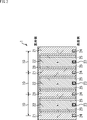
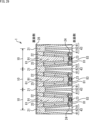
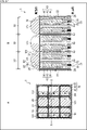
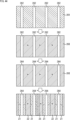
図1のAは、フォトダイオードアレイ1の半導体基板(半導体層)の平面図であり、図1のBは、フォトダイオードアレイ1の半導体基板の断面図である。図1のAは、半導体基板の表面側に相当する図1のBの断面図における下面の平面図であり、図1のBは、図1のAのX-X線における断面図である。 1A is a plan view of the semiconductor substrate (semiconductor layer) of the photodiode array 1, and FIG. 1B is a cross-sectional view of the semiconductor substrate of the photodiode array 1. FIG. 1A is a plan view of the lower surface of the cross-sectional view of FIG. 1B corresponding to the front surface side of the semiconductor substrate, and FIG. 1B is a cross-sectional view taken along line XX of FIG. 1A.
図1のフォトダイオードアレイ1は、画素10が3x3のマトリクス状に配置されて構成され、各画素10には、アバランシェフォトダイオード(以下、APDと称する。)が形成されている。図1のAにおいて破線は、各画素10の境界を示している。
The photodiode array 1 of FIG. 1 is configured by arranging
なお、図1のフォトダイオードアレイ1は、3x3の9個の画素で構成されているが、行方向および列方向の配列数並びに画素の総数は、これに限定されず任意である。 Although the photodiode array 1 in FIG. 1 is composed of 3×3=9 pixels, the number of arrays in the row direction and the column direction and the total number of pixels are not limited to this, and are arbitrary.
フォトダイオードアレイ1の各画素10は、第1導電型の第1半導体層21と、第2導電型の第2半導体層22を備える。
Each
より具体的には、図1のBに示されるように、各画素10において、画素境界を含む境界近傍の外周部に、第1導電型の第1半導体層21が形成され、第1導電型の第1半導体層21の内側に、第1導電型と反対の導電型である第2導電型の第2半導体層22が形成されている。
More specifically, as shown in FIG. 1B, in each
第1導電型としては、P型およびN型のどちらも取ることができ、例えば、第1導電型をP型とすると、第2導電型はN型となり、第1導電型をN型とすると、第2導電型はP型となる。 The first conductivity type can be either P-type or N-type. For example, if the first conductivity type is P-type, the second conductivity type is N-type, and if the first conductivity type is N-type, , the second conductivity type is P-type.
以下では、第1導電型をP型とし、第2導電型をN型とした場合について説明し、理解を容易にするため、第1半導体層21をP+型第1半導体層21、第2半導体層22をN+型第2半導体層22、のように、導電型と不純物濃度を付加して記述する。後述するその他の半導体層についても同様とする。
In the following, a case where the first conductivity type is the P type and the second conductivity type is the N type will be described. The
なお、不純物濃度については、P型の場合、“P++”、“P+”、“P”、“P-”のように記述し、“P++”の不純物濃度が最も高く、“P++”、“P+”、“P”、“P-”の順で不純物濃度が低いことを表す。N型の場合についても同様に、“N++”、“N+”、“N”、“N-”のように記述し、“N++”の不純物濃度が最も高く、“N++”、“N+”、“N”、“N-”の順で不純物濃度が低いことを表す。 Regarding the impurity concentration, in the case of P type, it is described as "P++", "P+", "P", "P-". ”, “P”, and “P-” indicate the lowest impurity concentration. Similarly, the N-type is described as "N++", "N+", "N", "N-", where "N++" has the highest impurity concentration, and "N++", "N+", " The impurity concentration is lower in the order of "N" and "N-".
図1のBの断面図の下面に相当する半導体基板の表面の、画素10の中央部には、逆バイアス電圧を印加する際のカソードとなるコンタクト23(以下、カソードコンタクト23という。)が、高濃度のN型の拡散層(N++)で形成されている。また、基板の表面の、画素10の境界部には、逆バイアス電圧を印加する際のアノードとなるコンタクト24(以下、アノードコンタクト24という。)が、高濃度のP型の拡散層(P++)で形成されている。
At the center of the
図1のAに示されるように、アノードコンタクト24は、画素10の境界部に沿って格子状に形成されており、画素単位には分離されていないのに対して、カソードコンタクト23が、画素10の中央部に画素単位に形成されている。光電変換された光信号は、カソードコンタクト23から出力される。
As shown in FIG. 1A, the
フォトダイオードアレイ1を構成する各画素10のアノードおよびカソードに、ブレークダウン電圧よりも高い逆バイアス電圧を印加すると、アバランシェ増倍が起こる領域である高電界領域25が、図1のBに示されるように、半導体基板の深さ方向に形成される。N+型第2半導体層22は、断面視において、P+型第1半導体層21内に縦長に形成されているので、高電界領域25が、長方形の長辺側に形成される。画素内に入射されたフォトンは、N+型第2半導体層22で光電変換されて正孔(キャリア)となり、正孔は、横方向に移動して高電界領域25で増倍される。
FIG. 1B shows a high
高電界領域25が、半導体基板の深さ方向に縦長に形成されるので、画素の平面サイズが小さくなった場合でも、基板深さ方向に、十分な高電界領域を確保することができる。また、高電界領域25が縦方向に形成されることで、ガードリングを横方向に形成しなくても、エッジのブレークダウンを回避することが可能となる。したがって、図1のフォトダイオードアレイ1の構造によれば、ガードリングが不要で、十分な高電界領域を確保しつつ、画素サイズを小さくすることができる。
Since the high
また、N+型第2半導体層22が縦長に形成されているので、フォトンの到達から増倍されるまでの距離は、長方形のN+型第2半導体層22の短辺に平行な方向の移動となり、短くなる。これにより、ジッター特性を改善することができる。
In addition, since the N + -type
なお、図1のフォトダイオードアレイ1において、光が入射される面は、半導体基板の表面または裏面のどちらにすることもできるが、光の入射面を、半導体基板の裏面側とする裏面照射型の場合には、図2に示されるように、裏面界面における暗電流の発生を抑制するための固定電荷膜28を裏面側界面に形成することが好ましい。この固定電荷膜28は、例えば、HfO2、Al2O3等の膜で形成することができる。
In the photodiode array 1 of FIG. 1, the surface on which light is incident can be either the front surface or the back surface of the semiconductor substrate. In this case, as shown in FIG. 2, it is preferable to form a fixed
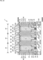
<2.第2実施の形態>
図3は、本技術を適用した光検出素子としてのフォトダイオードアレイの第2実施の形態の構成例を示している。<2. Second Embodiment>
FIG. 3 shows a configuration example of a second embodiment of a photodiode array as a photodetector to which the present technology is applied.
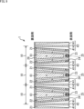
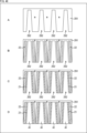
図3のAは、フォトダイオードアレイ1の半導体基板の平面図であり、図3のBは、フォトダイオードアレイ1の半導体基板の断面図である。図3の平面図および断面図における半導体基板の表裏の関係は、第1実施の形態と同様とする。 3A is a plan view of the semiconductor substrate of the photodiode array 1, and FIG. 3B is a cross-sectional view of the semiconductor substrate of the photodiode array 1. FIG. The relationship between the front and back surfaces of the semiconductor substrate in the plan view and cross-sectional view of FIG. 3 is the same as in the first embodiment.
図3においては、図1に示した第1実施の形態と対応する部分については同一の符号を付してあり、その部分の説明は適宜省略して、第2実施の形態が第1実施の形態と異なる部分について説明する。 In FIG. 3, parts corresponding to those of the first embodiment shown in FIG. The part different from the form will be explained.
第2実施の形態では、図1に示した第1実施の形態と比較すると、図3のAおよびBに示されるように、画素10の境界に、シリコン酸化膜(SiO2)などの絶縁膜41と、タングステン(W)、アルミニウム(Al)又は銅(Cu)などの金属膜42とからなる分離部43が新たに形成されている。分離部43は、隣接する画素間を絶縁分離する。高電界領域25は、分離部43に隣接して形成される。
In comparison with the first embodiment shown in FIG. 1, in the second embodiment, as shown in FIGS. and a
分離部43を半導体基板に形成することで、絶縁膜41と半導体基板との界面に発生する暗電流が懸念されるが、分離部43をP+型第1半導体層21内に形成することで、界面に起因する暗電流を抑制することができる。また、分離部43を画素境界に設けたことにより、クロストークの発生も抑制することができる。
By forming the
したがって、画素境界に分離部43を設けたことにより、微細画素で問題となるクロストークと界面の暗電流に起因するダークカウントレート(以下、DCRと称する。)を低減することができる。
Therefore, by providing the separating
分離部43は、金属膜42を省略して、絶縁膜41のみで形成してもよいが、絶縁膜41の内部に金属膜42を設けることで、遮光性を向上させることができる。また、金属膜42にアノードと同電位の電圧を印加すると、P+型第1半導体層21との界面で発生する暗電流をさらに抑制することができる。
The
なお、図3のフォトダイオードアレイ1においても、光が入射される面は、半導体基板の表面または裏面のどちらでもよい。裏面照射型の場合には、図2と同じように、固定電荷膜28を半導体基板の裏面側界面に形成することが好ましい。
In the photodiode array 1 of FIG. 3 as well, the surface on which light is incident may be either the front surface or the rear surface of the semiconductor substrate. In the case of the backside irradiation type, it is preferable to form the fixed
また、分離部43の断面形状は、図4のように、裏面側と表面側の平面領域面積が異なるテーパ形状となっていてもよい。
Moreover, the cross-sectional shape of the separating
図4は、絶縁膜41および金属膜42を埋め込むためのトレンチを、表面側から形成した場合の分離部43の形成例を示しており、この場合、分離部43の断面形状は、裏面側から表面側に行くほど平面領域面積が大きくなる下広がりのテーパ形状となる。反対に、図示は省略するが、絶縁膜41および金属膜42を埋め込むためのトレンチを、裏面側から形成した場合には、分離部43の断面形状は、裏面側から表面側に行くほど平面領域面積が小さくなる下すぼみのテーパ形状となる。
FIG. 4 shows an example of formation of the
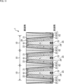
<3.第3実施の形態>
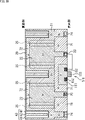
図5は、本技術を適用した光検出素子としてのフォトダイオードアレイの第3実施の形態の構成例を示している。<3. Third Embodiment>
FIG. 5 shows a configuration example of a third embodiment of a photodiode array as a photodetector to which the present technology is applied.
図5のAは、フォトダイオードアレイ1の半導体基板の平面図であり、図5のBは、フォトダイオードアレイ1の半導体基板の断面図である。図5の平面図および断面図における半導体基板の表裏の関係は、第1実施の形態と同様とする。 5A is a plan view of the semiconductor substrate of the photodiode array 1, and FIG. 5B is a cross-sectional view of the semiconductor substrate of the photodiode array 1. FIG. The relationship between the front and back surfaces of the semiconductor substrate in the plan view and cross-sectional view of FIG. 5 is the same as in the first embodiment.
図5においては、図3に示した第2実施の形態と対応する部分については同一の符号を付してあり、その部分の説明は適宜省略して、第3実施の形態が第2実施の形態と異なる部分について説明する。 In FIG. 5, parts corresponding to those of the second embodiment shown in FIG. The part different from the form will be explained.
図5に示されるフォトダイオードアレイ1は、図3に示した第2実施の形態に係るフォトダイオードアレイ1を、裏面照射型に特化した構造であり、図3の構成に対して、固定電荷膜29が、新たに追加されている。
The photodiode array 1 shown in FIG. 5 has a structure in which the photodiode array 1 according to the second embodiment shown in FIG. A
固定電荷膜29は、半導体基板の裏面側界面に形成され、裏面側界面で発生する暗電流を抑制することができる。分離部43がある部分では、固定電荷膜29は、P+型第1半導体層21と絶縁膜41との間に形成されており、分離部43とP+型第1半導体層21との界面で発生する暗電流を抑制する。
The fixed
分離部43の断面形状は、第2実施の形態と同様にテーパ形状となっていてもよい。分離部43の断面形状をテーパ形状とする場合には、絶縁膜41および金属膜42を埋め込むためのトレンチを、裏面側から形成するため、図6のように、下すぼみのテーパ形状となる。
The cross-sectional shape of the
<4.第4実施の形態>
図7は、本技術を適用した光検出素子としてのフォトダイオードアレイの第4実施の形態の構成例を示している。<4. Fourth Embodiment>
FIG. 7 shows a configuration example of a fourth embodiment of a photodiode array as a photodetector to which the present technology is applied.
図7のAは、フォトダイオードアレイ1の半導体基板の平面図であり、図7のBは、フォトダイオードアレイ1の半導体基板の断面図である。図7のAの平面図は、図7のBのY-Y線における平面図である。 7A is a plan view of the semiconductor substrate of the photodiode array 1, and FIG. 7B is a cross-sectional view of the semiconductor substrate of the photodiode array 1. FIG. A plan view of FIG. 7A is a plan view taken along line Y-Y of FIG. 7B.
図7のBに示される断面図では、半導体基板の裏面界面に、暗電流抑制のための固定電荷膜28が形成されており、図7は、裏面照射型の構成例を示している。
In the cross-sectional view shown in FIG. 7B, a fixed
図2に示した第1実施の形態の裏面照射型の構成では、カソードコンタクト23に接続されるN+型第2半導体層22が、領域内で均一かつ高濃度なN型不純物領域で形成されていた。
In the back-illuminated structure of the first embodiment shown in FIG. 2, the N + -type
これに対して、図7に示される第4実施の形態では、カソードコンタクト23に接続されるN+型第2半導体層22の内側に、それよりも低濃度のN型(N-)の第3半導体層61(以下、N-型第3半導体層61という。)が形成されている。N-型第3半導体層61は、図7のAに示されるように、平面視において、高濃度なN+型第2半導体層22の内側で、画素10の中央部に形成されている。
On the other hand, in the fourth embodiment shown in FIG. 7, an N-type (N−)
図7の第4実施の形態のその他の構成は、図2に示した第1実施の形態の裏面照射型の構成と同様であるので、説明を省略する。 Other configurations of the fourth embodiment shown in FIG. 7 are the same as those of the back-illuminated type configuration of the first embodiment shown in FIG. 2, so description thereof will be omitted.
第4実施の形態のように、平面視において画素中央部に低濃度のN-型第3半導体層61を配置し、その外側、換言すれば、PN接合が配置される方向に、高濃度なN+型第2半導体層22を配置することにより、平面方向に形成される電位勾配(ポテンシャル勾配)によって、入射光の光電変換によって発生した電荷を、高濃度なN+型第2半導体層22に効率的に取り込むことができる。
As in the fourth embodiment, the low-concentration N− type
なお、このように、カソードコンタクト23に接続されるN型不純物領域を、高濃度なN+型第2半導体層22と、その内側のN-型第3半導体層61とで構成する構造は、上述した第2および第3実施の形態にも適用することができる。
The structure in which the N-type impurity region connected to the
図8は、図3に示した分離部43を有する第2実施の形態のフォトダイオードアレイ1に、第4実施の形態の特徴的構成を追加した構成例を示す断面図である。
FIG. 8 is a cross-sectional view showing a configuration example in which the characteristic configuration of the fourth embodiment is added to the photodiode array 1 of the second embodiment having the
図8では、図3に示したフォトダイオードアレイ1のN+型第2半導体層22の内側に、N-型第3半導体層61が追加されている。
In FIG. 8, an N− type
図9は、図4に示したテーパ形状の分離部43を有する第2実施の形態のフォトダイオードアレイ1に、第4実施の形態の特徴的構成を追加した構成例を示す断面図である。
FIG. 9 is a cross-sectional view showing a configuration example in which the characteristic configuration of the fourth embodiment is added to the photodiode array 1 of the second embodiment having the tapered
図9では、図3に示したフォトダイオードアレイ1のN+型第2半導体層22の内側に、N-型第3半導体層61が追加されている。なお、図8および図9は、裏面照射型の例であり、裏面側界面に固定電荷膜28も形成されている。
In FIG. 9, an N− type
図10は、図5に示した固定電荷膜29を有する第3実施の形態のフォトダイオードアレイ1に、第4実施の形態の特徴的構成を追加した構成例を示す断面図である。
FIG. 10 is a cross-sectional view showing a configuration example in which the characteristic configuration of the fourth embodiment is added to the photodiode array 1 of the third embodiment having the fixed
図10では、図5に示したフォトダイオードアレイ1のN+型第2半導体層22の内側に、N-型第3半導体層61が追加されている。
In FIG. 10, an N− type
図11は、図6に示したテーパ形状の分離部43を有する第3実施の形態のフォトダイオードアレイ1に、第4実施の形態の特徴的構成を追加した構成例を示す断面図である。
FIG. 11 is a cross-sectional view showing a configuration example in which the characteristic configuration of the fourth embodiment is added to the photodiode array 1 of the third embodiment having the tapered
図11では、図6に示したフォトダイオードアレイ1のN+型第2半導体層22の内側に、N-型第3半導体層61が追加されている。
In FIG. 11, an N− type
図8乃至図11のいずれの構成においても、平面方向に形成される電位勾配により、入射光の光電変換によって発生した電荷を、高濃度なN+型第2半導体層22に効率的に取り込むことができる。
8 to 11, electric charges generated by photoelectric conversion of incident light can be efficiently taken into the high-concentration N + -type
なお、図8乃至図11は、いずれも、裏面照射型の例であるが、表面照射型に適用することも勿論可能である。 Although FIGS. 8 to 11 are all examples of the back irradiation type, they can of course be applied to the front irradiation type.
<5.第5実施の形態>
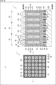
図12は、本技術を適用した光検出素子としてのフォトダイオードアレイの第5実施の形態の構成例を示している。<5. Fifth Embodiment>
FIG. 12 shows a configuration example of a fifth embodiment of a photodiode array as a photodetector to which the present technology is applied.
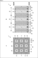
図12のAは、フォトダイオードアレイ1の半導体基板の平面図であり、図12のBは、フォトダイオードアレイ1の半導体基板の断面図である。図12の平面図および断面図における半導体基板の表裏の関係は、第1実施の形態と同様とする。 12A is a plan view of the semiconductor substrate of the photodiode array 1, and FIG. 12B is a cross-sectional view of the semiconductor substrate of the photodiode array 1. FIG. The relationship between the front and back surfaces of the semiconductor substrate in the plan view and cross-sectional view of FIG. 12 is the same as in the first embodiment.
図12においては、上述した第1乃至第4実施の形態と対応する部分については同一の符号を付してあり、その部分の説明は適宜省略して、異なる部分について説明する。 In FIG. 12, the same reference numerals are given to the parts corresponding to those of the above-described first to fourth embodiments, and the description of those parts will be omitted as appropriate, and the different parts will be described.
図12のBの断面図を、図8に示した第4実施の形態の断面図と比較すると、第5実施の形態では、半導体基板の表面側に、STI(Shallow Trench Isolation)63が新たに追加されている。STI63は、P+型第1半導体層21に接続されるアノードコンタクト24と、N+型第2半導体層22に接続されるカソードコンタクト23とを電気的に分離する。また、STI63は、高電界領域25を形成するP+型第1半導体層21とN+型第2半導体層22の界面が、半導体基板の表面に接することを回避する。これにより、半導体基板の表面で発生する暗電流が増倍されることを抑制することができる。
Comparing the cross-sectional view of B in FIG. 12 with the cross-sectional view of the fourth embodiment shown in FIG. Added. The
なお、図12に示した構成例では、基板表面のカソードコンタクト23とSTI63の間に、N+型第2半導体層22が配置されているが、基板表面のカソードコンタクト23とアノードコンタクト24の間を、すべてSTI63で形成して、N+型第2半導体層22が基板表面に露出されない構成としてもよい。
In the configuration example shown in FIG. 12, the N + -type
<6.第6実施の形態>
図13は、本技術を適用した光検出素子としてのフォトダイオードアレイの第6実施の形態の構成例を示している。<6. Sixth Embodiment>
FIG. 13 shows a configuration example of a sixth embodiment of a photodiode array as a photodetector to which the present technology is applied.
図13のAは、フォトダイオードアレイ1の半導体基板の平面図であり、図13のBは、フォトダイオードアレイ1の半導体基板の断面図である。図13のAは、半導体基板の表面側に相当する図13のBの断面図における下面の平面図であり、図13のBは、図13のAのZ-Z線における断面図である。 13A is a plan view of the semiconductor substrate of the photodiode array 1, and FIG. 13B is a cross-sectional view of the semiconductor substrate of the photodiode array 1. FIG. 13A is a plan view of the lower surface of the cross-sectional view of FIG. 13B corresponding to the front surface side of the semiconductor substrate, and FIG. 13B is a cross-sectional view taken along line ZZ of FIG. 13A.
図13においては、上述した第1乃至第5実施の形態と対応する部分については同一の符号を付してあり、その部分の説明は適宜省略して、異なる部分について説明する。 In FIG. 13, portions corresponding to those of the first to fifth embodiments described above are denoted by the same reference numerals, and descriptions of those portions are omitted as appropriate, and different portions are described.
図13のBの断面図を、図8に示した第4実施の形態の断面図と比較すると、図8では、アノードコンタクト24が、画素境界に形成された両側の分離部43それぞれに隣接して形成されているのに対して、図13では、アノードコンタクト24が、両側の分離部43の一方のみに隣接して形成されている。そして、カソードコンタクト23が、画素10の中央部ではなく、アノードコンタクト24が形成されていない方の分離部43側にシフトして配置されている。
Comparing the cross-sectional view of FIG. 13B with the cross-sectional view of the fourth embodiment shown in FIG. 8, in FIG. 13, the
図13のAの平面図で見ると、アノードコンタクト24は、矩形の画素10の1つの角(図13のAにおいて左上)の分離部43に接して配置されており、カソードコンタクト23は、N+型第2半導体層22の中央部(画素中央部)より、アノードコンタクト24が配置されている角と対角にある角に近い位置にシフトして配置されている。
13A, the
このように、第6実施の形態では、カソードコンタクト23とアノードコンタクト24を、矩形の画素10の平面領域内の対角方向に配置することで、画素内の可能な範囲でカソードコンタクト23とアノードコンタクト24の距離を離すことができる。これにより、半導体基板の表面側において、N型とP型の高濃度層であるカソードコンタクト23とアノードコンタクト24が接近することによって、高電界領域25よりも電界が高くなることを回避することができ、意図しないブレークダウンを抑制することができる。
As described above, in the sixth embodiment, by arranging the
<7.第7実施の形態>
図14は、本技術を適用した光検出素子としてのフォトダイオードアレイの第7実施の形態の構成例を示している。<7. Seventh Embodiment>
FIG. 14 shows a configuration example of a seventh embodiment of a photodiode array as a photodetector to which the present technology is applied.
図14のAは、フォトダイオードアレイ1の半導体基板の平面図であり、図14のBは、フォトダイオードアレイ1の半導体基板の断面図である。図14のAは、半導体基板の表面側に相当する図14のBの断面図における下面の平面図であり、図14のBは、図14のAのZ-Z線における断面図である。 14A is a plan view of the semiconductor substrate of the photodiode array 1, and FIG. 14B is a cross-sectional view of the semiconductor substrate of the photodiode array 1. FIG. 14A is a plan view of the lower surface of the cross-sectional view of FIG. 14B corresponding to the front surface side of the semiconductor substrate, and FIG. 14B is a cross-sectional view taken along line ZZ of FIG. 14A.
図14においては、上述した第1乃至第6実施の形態と対応する部分については同一の符号を付してあり、その部分の説明は適宜省略して、異なる部分について説明する。 In FIG. 14, the same reference numerals are given to the parts corresponding to those of the first to sixth embodiments described above, and the description of those parts will be omitted as appropriate, and the different parts will be described.
図14の第7実施の形態は、図12の第5実施の形態と、図13の第6実施の形態の両方の特徴的構成を備える形態である。 The seventh embodiment shown in FIG. 14 has the characteristic configuration of both the fifth embodiment shown in FIG. 12 and the sixth embodiment shown in FIG.
即ち、図14の第7実施の形態では、図12の第5実施の形態と同様に、STI63が設けられている。STI63は、半導体基板の表面側に、P+型第1半導体層21に接続されるアノードコンタクト24と、N+型第2半導体層22に接続されるカソードコンタクト23とを電気的に分離する。また、図14の第7実施の形態では、図13の第6実施の形態と同様に、カソードコンタクト23とアノードコンタクト24が、矩形の画素10の平面領域内の対角方向に配置されている。
That is, in the seventh embodiment shown in FIG. 14, an
これにより、半導体基板の表面で発生する暗電流が増倍されることを抑制することができる。また、半導体基板の表面側において、カソードコンタクト23とアノードコンタクト24が接近することによって、高電界領域25よりも電界が高くなることを回避することができ、意図しないブレークダウンを抑制することができる。
Thereby, it is possible to suppress the dark current generated on the surface of the semiconductor substrate from being multiplied. Further, on the surface side of the semiconductor substrate, the
<8.第8実施の形態>
図15は、本技術を適用した光検出素子としてのフォトダイオードアレイの第8実施の形態の構成例を示している。<8. Eighth Embodiment>
FIG. 15 shows a configuration example of an eighth embodiment of a photodiode array as a photodetector to which the present technology is applied.
図15のAは、フォトダイオードアレイ1の半導体基板の平面図であり、図15のBは、フォトダイオードアレイ1の半導体基板の断面図である。図15のAは、半導体基板の表面側に相当する図15のBの断面図における下面の平面図であり、図15のBは、図15のAのX-X線における断面図である。 15A is a plan view of the semiconductor substrate of the photodiode array 1, and FIG. 15B is a cross-sectional view of the semiconductor substrate of the photodiode array 1. FIG. 15A is a plan view of the lower surface of the cross-sectional view of FIG. 15B corresponding to the front surface side of the semiconductor substrate, and FIG. 15B is a cross-sectional view taken along line XX of FIG. 15A.
図15のBに示される断面図では、半導体基板の裏面側界面に、暗電流抑制のための固定電荷膜28が形成されており、図15は、裏面照射型の構成例を示している。
In the cross-sectional view shown in FIG. 15B, a fixed
図15に示される第8実施の形態では、図2に示した第1実施の形態の構成と比較して、N+型第2半導体層22と半導体基板の表面との間に、N+型第2半導体層22よりも不純物濃度の低いN型の第4半導体層71(以下、N-型第4半導体層71という。)が形成されている。また、N+型第2半導体層22と半導体基板の裏面との間に、N+型第2半導体層22よりも不純物濃度の低いN型の第5半導体層72(以下、N-型第5半導体層72という。)が形成されている。N-型第4半導体層71とN-型第5半導体層72の不純物濃度は、N+型第2半導体層22よりも低ければよく、同じ濃度である必要はない。
In the eighth embodiment shown in FIG. 15, compared with the configuration of the first embodiment shown in FIG. 2, an N + -type
N-型第4半導体層71は、平面方向においては、図15のAに示されるように、N+型第2半導体層22とP+型第1半導体層21の間に、同心矩形状に形成されている。N-型第5半導体層72は、接するN+型第2半導体層22と同じ平面領域に形成されている。
The N− type
図15の第8実施の形態のその他の構成は、図2に示した第1実施の形態の裏面照射型の構成と同様であるので、説明を省略する。 Other configurations of the eighth embodiment shown in FIG. 15 are the same as those of the back-illuminated type configuration of the first embodiment shown in FIG.
N+型第2半導体層22と半導体基板の表面との間に、N+型第2半導体層22よりも不純物濃度が低いN-型第4半導体層71を形成することにより、高電界領域25を形成するP+型第1半導体層21とN+型第2半導体層22の界面が、半導体基板の表面に接することを回避する。これにより、半導体基板の表面で発生する暗電流が増倍されることを抑制することができる。
A high
N+型第2半導体層22と半導体基板の裏面との間に、N+型第2半導体層22よりも不純物濃度が低いN-型第5半導体層72を形成することにより、高電界領域25を形成するP+型第1半導体層21とN+型第2半導体層22の界面が、半導体基板の裏面に接することを回避する。これにより、半導体基板の裏面で発生する暗電流が増倍されることを抑制することができる。
A high
なお、このように、N+型第2半導体層22の基板深さ方向に隣接してN-型第4半導体層71およびN-型第5半導体層72を配置する構造は、上述したその他の実施の形態にも適用することができる。
The structure in which the N − -type
図16は、図3に示した分離部43を有する第2実施の形態のフォトダイオードアレイ1に、第8実施の形態の特徴的構成を追加した構成例を示す断面図である。
FIG. 16 is a cross-sectional view showing a configuration example in which the characteristic configuration of the eighth embodiment is added to the photodiode array 1 of the second embodiment having the
図16では、図3に示したフォトダイオードアレイ1の高電界領域25を形成するN+型第2半導体層22の基板深さ方向の長さが短くなり、N+型第2半導体層22の基板表面側と裏面側に隣接して、N-型第4半導体層71およびN-型第5半導体層72が追加されている。
In FIG. 16, the length in the substrate depth direction of the N + -type
図17は、図5に示した固定電荷膜29を有する第3実施の形態のフォトダイオードアレイ1に、第8実施の形態の特徴的構成を追加した構成例を示す断面図である。
FIG. 17 is a cross-sectional view showing a configuration example in which the characteristic configuration of the eighth embodiment is added to the photodiode array 1 of the third embodiment having the fixed
図17では、図5に示したフォトダイオードアレイ1の高電界領域25を形成するN+型第2半導体層22の基板深さ方向の長さが短くなり、N+型第2半導体層22の基板表面側と裏面側に隣接して、N-型第4半導体層71およびN-型第5半導体層72が追加されている。
In FIG. 17, the length in the substrate depth direction of the N + -type
図18は、図9に示した、テーパ形状の分離部43と、画素中央部に低濃度のN-型第3半導体層61を有する第4実施の形態のフォトダイオードアレイ1に、第8実施の形態の特徴的構成を追加した構成例を示す断面図である。
FIG. 18 shows the photodiode array 1 of the fourth embodiment, which has the tapered
図18では、図9に示したフォトダイオードアレイ1の高電界領域25を形成するN+型第2半導体層22の基板深さ方向の長さが短くなり、N+型第2半導体層22の基板表面側と裏面側に隣接して、N-型第4半導体層71およびN-型第5半導体層72が追加されている。
In FIG. 18, the length in the substrate depth direction of the N + -type
図19は、図11に示したテーパ形状の分離部43と、画素中央部に低濃度のN-型第3半導体層61を有する第4実施の形態のフォトダイオードアレイ1に、第8実施の形態の特徴的構成を追加した構成例を示す断面図である。
FIG. 19 shows the photodiode array 1 of the fourth embodiment, which has the tapered
図19では、図11に示したフォトダイオードアレイ1の高電界領域25を形成するN+型第2半導体層22の基板深さ方向の長さが短くなり、N+型第2半導体層22の基板表面側と裏面側に隣接して、N-型第4半導体層71およびN-型第5半導体層72が追加されている。
In FIG. 19, the length in the substrate depth direction of the N + -type
図16乃至図19のいずれの構成においても、N-型第4半導体層71およびN-型第5半導体層72を設けることにより、半導体基板の表面および裏面で発生する暗電流が増倍されることを抑制することができる。
16 to 19, dark current generated on the front and back surfaces of the semiconductor substrate is multiplied by providing the N-type
<9.第9実施の形態>
図20は、本技術を適用した光検出素子としてのフォトダイオードアレイの第9実施の形態の構成例を示している。<9. Ninth Embodiment>
FIG. 20 shows a configuration example of a ninth embodiment of a photodiode array as a photodetector to which the present technology is applied.
第9実施の形態については、図15乃至図19で示した第8実施の形態と比較して、説明する。 The ninth embodiment will be described in comparison with the eighth embodiment shown in FIGS. 15 to 19. FIG.
図20に示される第9実施の形態に係るフォトダイオードアレイ1では、図15に示した第8実施の形態においてN+型第2半導体層22の基板表面側と基板裏面側に隣接して形成されていたN-型第4半導体層71およびN-型第5半導体層72の領域に、P+型第1半導体層21よりも不純物濃度の低いP型の第6半導体層81(以下、P-型第6半導体層81という。)および第7半導体層82(以下、P-型第7半導体層82という。)が形成されている。
In the photodiode array 1 according to the ninth embodiment shown in FIG. 20, the N + -type
なお、P-型第6半導体層81とN+型第2半導体層22との間に、低濃度のN型(N-型)の第8半導体層83(以下、N-型第8半導体層83という。)が薄い膜厚で挿入されているが、このN-型第8半導体層83は、P-型第6半導体層81に置き換えてもよい。
A low-concentration N-type (N-type) eighth semiconductor layer 83 (hereinafter referred to as N-type eighth semiconductor layer 83 ) is inserted with a thin film thickness, the N − -type
また、P-型第7半導体層82の平面方向内側に、低濃度のN型(N-型)の第9半導体層84(以下、N-型第9半導体層84という。)が形成されているが、このN-型第9半導体層84は、P-型第7半導体層82に置き換えてもよい。
A low-concentration N-type (N-type) ninth semiconductor layer 84 (hereinafter referred to as N-type ninth semiconductor layer 84) is formed inside the P-type
図21に示される第9実施の形態に係るフォトダイオードアレイ1は、図16に示した第8実施の形態の構成例に対応する。図16のN+型第2半導体層22の基板表面側と裏面側に隣接して形成されていたN-型第4半導体層71およびN-型第5半導体層72が、図21では、P-型第6半導体層81およびP-型第7半導体層82と、N-型第8半導体層83およびN-型第9半導体層84に置き換えられている。
The photodiode array 1 according to the ninth embodiment shown in FIG. 21 corresponds to the configuration example of the eighth embodiment shown in FIG. The N− type
図22に示される第9実施の形態に係るフォトダイオードアレイ1は、図17に示した第8実施の形態の構成例に対応する。図17のN+型第2半導体層22の基板表面側と裏面側に隣接して形成されていたN-型第4半導体層71およびN-型第5半導体層72が、図22では、P-型第6半導体層81およびP-型第7半導体層82と、N-型第8半導体層83およびN-型第9半導体層84に置き換えられている。
The photodiode array 1 according to the ninth embodiment shown in FIG. 22 corresponds to the configuration example of the eighth embodiment shown in FIG. The N− type
図23に示される第9実施の形態に係るフォトダイオードアレイ1は、図18に示した第8実施の形態の構成例に対応する。図18のN+型第2半導体層22の基板表面側と裏面側に隣接して形成されていたN-型第4半導体層71およびN-型第5半導体層72が、図23では、P-型第6半導体層81およびP-型第7半導体層82と、N-型第8半導体層83およびN-型第9半導体層84に置き換えられている。なお、図23において、N-型第9半導体層84は、同型および同濃度のN-型第3半導体層61として図示されている。
The photodiode array 1 according to the ninth embodiment shown in FIG. 23 corresponds to the configuration example of the eighth embodiment shown in FIG. The N− type
図24に示される第9実施の形態に係るフォトダイオードアレイ1は、図19に示した第8実施の形態の構成例に対応する。図19のN+型第2半導体層22の基板表面側に隣接して形成されていたN-型第4半導体層71が、図24では、P-型第6半導体層81に置き換えられている。
The photodiode array 1 according to the ninth embodiment shown in FIG. 24 corresponds to the configuration example of the eighth embodiment shown in FIG. The N− type
なお、図21乃至図23において、N-型第8半導体層83および-型第9半導体層84をそれぞれ、P-型第6半導体層81およびP-型第7半導体層82に置き換えてもよい点は、図20と同様である。
21 to 23, the N-type
図21乃至図24の第9実施の形態によれば、N+型第2半導体層22と半導体基板の表面との間に、N+型第2半導体層22よりも不純物濃度が低いP-型第6半導体層81を形成することにより、高電界領域25を形成するP+型第1半導体層21とN+型第2半導体層22の界面が、半導体基板の表面に接することを回避する。これにより、半導体基板の表面で発生する暗電流が増倍されることを抑制することができる。
According to the ninth embodiment shown in FIGS. 21 to 24, a P − -type sixth semiconductor layer having a lower impurity concentration than the N + -type
N+型第2半導体層22と半導体基板の裏面との間に、N+型第2半導体層22よりも不純物濃度が低いP-型第7半導体層82を形成することにより、高電界領域25を形成するP+型第1半導体層21とN+型第2半導体層22の界面が、半導体基板の裏面に接することを回避する。これにより、半導体基板の裏面で発生する暗電流が増倍されることを抑制することができる。
A high
<10.第10実施の形態>
図25は、本技術を適用した光検出素子としてのフォトダイオードアレイの第10実施の形態の構成例を示している。<10. Tenth Embodiment>
FIG. 25 shows a configuration example of a tenth embodiment of a photodiode array as a photodetector to which the present technology is applied.
図25のAは、フォトダイオードアレイ1の半導体基板の平面図であり、図25のBは、フォトダイオードアレイ1の半導体基板の断面図である。図25のAは、半導体基板の表面側に相当する図25のBの断面図における下面の平面図であり、図25のBは、図25のAのX-X線における断面図である。 25A is a plan view of the semiconductor substrate of the photodiode array 1, and FIG. 25B is a cross-sectional view of the semiconductor substrate of the photodiode array 1. FIG. 25A is a plan view of the lower surface of the cross-sectional view of FIG. 25B corresponding to the front surface side of the semiconductor substrate, and FIG. 25B is a cross-sectional view taken along line XX of FIG. 25A.
図25に示される第10実施の形態は、図21に示した第9実施の形態と比較して、N+型第2半導体層22の領域内の濃度分布が異なる。
The tenth embodiment shown in FIG. 25 differs from the ninth embodiment shown in FIG. 21 in the concentration distribution within the region of the N + -type
具体的には、図21に示した第9実施の形態では、N+型第2半導体層22の領域内の不純物濃度が、均一に形成されていた。
Specifically, in the ninth embodiment shown in FIG. 21, the impurity concentration in the region of the N + -type
これに対して、図25の第10実施の形態では、基板深さ方向に対しては、基板裏面から基板表面に向かって不純物濃度が濃くなり、基板表面において、カソードコンタクト23の不純物濃度となる。また、基板深さ方向に直交する平面方向に対しては、画素中央部から、画素境界に向かって不純物濃度が濃くなり、P+型第1半導体層21とN+型第2半導体層22との界面においては、高電界領域25を形成するのに十分な高濃度となっている。
On the other hand, in the tenth embodiment shown in FIG. 25, in the substrate depth direction, the impurity concentration increases from the substrate back surface toward the substrate surface, and reaches the impurity concentration of the
平面方向に電位勾配を形成することにより、図7等で示した第4実施の形態と同様に、入射光の光電変換によって発生した電荷を、高電界領域25に効率的に取り込むことができる。
By forming a potential gradient in the plane direction, electric charges generated by photoelectric conversion of incident light can be efficiently taken into the high
また、基板深さ方向に電位勾配を形成することにより、高電界領域25で増倍された電荷を、カソードコンタクト23に効率的に収集することができる。
Further, by forming a potential gradient in the depth direction of the substrate, charges multiplied in the high
<11.第11実施の形態>
図26は、本技術を適用した光検出素子としてのフォトダイオードアレイの第11実施の形態の構成例を示している。<11. Eleventh Embodiment>
FIG. 26 shows a configuration example of an eleventh embodiment of a photodiode array as a photodetector to which the present technology is applied.
第11実施の形態については、図20乃至図24で示した第9実施の形態と比較して、説明する。 The eleventh embodiment will be described in comparison with the ninth embodiment shown in FIGS.
図26に示される第11実施の形態に係るフォトダイオードアレイ1では、図20に示した第9実施の形態において、N+型第2半導体層22の基板裏面側に隣接して形成されていたP-型第7半導体層82およびN-型第9半導体層84が、低濃度のN型(N-型)の第10半導体層91(以下、N-型第10半導体層91という。)に置き換えられている。N-型第10半導体層91は、図20のP-型第7半導体層82およびN-型第9半導体層84よりも、基板深さ方向の厚みが厚く形成されており、その分、高電界領域25の基板深さ方向の領域長さが短く形成されている。
In the photodiode array 1 according to the eleventh embodiment shown in FIG. 26, in the ninth embodiment shown in FIG. The − type
このように、高電界領域25の基板深さ方向の領域長さを短く形成し、基板表面および基板裏面から離すことにより、高電界領域25を形成するP+型第1半導体層21とN+型第2半導体層22の界面が、半導体基板の表面および裏面に接することを回避する。これにより、半導体基板の表面および裏面で発生する暗電流が増倍されることを抑制することができる。
In this way, the length of the high
図27に示される第11実施の形態に係るフォトダイオードアレイ1は、図21に示した第9実施の形態の構成例に対応する。図21においてN+型第2半導体層22の基板裏面側に隣接して形成されていたP-型第7半導体層82およびN-型第9半導体層84が、図27では、N-型第10半導体層91に置き換えられている。また、画素10の境界に形成されている分離部43が、基板表面側から、高電界領域25の基板深さ方向の領域長さに対応して形成されている。
The photodiode array 1 according to the eleventh embodiment shown in FIG. 27 corresponds to the configuration example of the ninth embodiment shown in FIG. The P − -type
図28に示される第11実施の形態に係るフォトダイオードアレイ1は、図22に示した第9実施の形態の構成例に対応する。図22において画素10の境界に形成されている分離部43が、図28では、基板裏面側から、高電界領域25の基板深さ方向の領域長さに対応して形成されている。
The photodiode array 1 according to the eleventh embodiment shown in FIG. 28 corresponds to the configuration example of the ninth embodiment shown in FIG. In FIG. 28, the separating
図29に示される第11実施の形態に係るフォトダイオードアレイ1は、図23に示した第9実施の形態の構成例に対応する。図23においてN+型第2半導体層22の基板裏面側に隣接して形成されていたN-型第3半導体層61およびP-型第7半導体層82が、図29では、N-型第10半導体層91に置き換えられている。また、画素10の境界に形成されている分離部43が、基板表面側から、高電界領域25の基板深さ方向の領域長さに対応して形成されている。
The photodiode array 1 according to the eleventh embodiment shown in FIG. 29 corresponds to the configuration example of the ninth embodiment shown in FIG. The N− type
図30に示される第11実施の形態に係るフォトダイオードアレイ1は、図24に示した第9実施の形態の構成例に対応する。図23においてN+型第2半導体層22の基板裏面側に隣接して形成されていたN-型第5半導体層72が、図30では、P-型第7半導体層82に置き換えられている。また、画素10の境界に形成されている分離部43が、基板裏面側から、高電界領域25の基板深さ方向の領域長さに対応して形成されている。
The photodiode array 1 according to the eleventh embodiment shown in FIG. 30 corresponds to the configuration example of the ninth embodiment shown in FIG. The N − -type
図26乃至図30の第11実施の形態によれば、高電界領域25の基板深さ方向の領域長さを短く形成し、基板表面および基板裏面から離すことにより、高電界領域25を形成するP+型第1半導体層21とN+型第2半導体層22の界面が、半導体基板の表面および裏面に接することを回避する。これにより、半導体基板の表面および裏面で発生する暗電流が増倍されることを抑制することができる。高電界領域25の領域面積が小さくなるほど、DCRが改善することができるので、DCRを向上させることができる。
According to the eleventh embodiment shown in FIGS. 26 to 30, the high
<12.第12実施の形態>
図31乃至図38で説明する第12乃至第15実施の形態は、光の入射面側にOCL(On Chip Lenz)を追加した構成例を示している。図31乃至図38において、半導体基板内の構成については、図21に示した第9実施の形態の構成を採用した例で説明するが、その他の実施の形態の構成も採用可能である。<12. 12th Embodiment>
The twelfth to fifteenth embodiments described with reference to FIGS. 31 to 38 show configuration examples in which an OCL (On Chip Lenz) is added to the light incident surface side. 31 to 38, the internal configuration of the semiconductor substrate will be described using an example employing the configuration of the ninth embodiment shown in FIG. 21, but configurations of other embodiments can also be employed.
図31は、本技術を適用した光検出素子としてのフォトダイオードアレイの第12実施の形態の構成例を示している。 FIG. 31 shows a configuration example of a twelfth embodiment of a photodiode array as a photodetector to which the present technology is applied.
図31のAは、フォトダイオードアレイ1の半導体基板の表面側の平面図であり、図31のBは、図31のAのX-X線における断面図である。 31A is a plan view of the photodiode array 1 on the front side of the semiconductor substrate, and FIG. 31B is a cross-sectional view taken along line X-X of FIG. 31A.
図31の第12実施の形態では、配線層102が形成された半導体基板の表面側に、OCL101が、1画素単位に形成されている。したがって、図31のフォトダイオードアレイ1は、光の入射面が半導体基板の表面である表面照射型の例である。なお、図31のAの平面図では、配線層102の図示は省略されている。
In the twelfth embodiment shown in FIG. 31, the
このように、光の入射面側に、OCL101を形成することで、入射光を、高電界領域25に効率的に取り込むことができ、感度を向上させることができる。
By forming the
図32は、裏面照射型とした場合の第12実施の形態に係るフォトダイオードアレイ1の構成例を示している。 FIG. 32 shows a configuration example of the photodiode array 1 according to the twelfth embodiment in the case of a back-illuminated type.
第12実施の形態において、光の入射面を半導体基板の裏面とした場合、裏面の固定電荷膜28の上面に、OCL101が、1画素単位に形成される。半導体基板裏面の画素境界には、タングステン(W)、アルミニウム(Al)又は銅(Cu)などの金属材料を用いた画素間遮光膜103も設けられている。
In the twelfth embodiment, when the light incident surface is the back surface of the semiconductor substrate, the
光の入射面が半導体基板の裏面である裏面照射型とした場合には、光路上に配線層102が存在しないので、配線層102による光のケラレを抑制することができ、さらに感度を向上させることができる。
In the case of a back-illuminated type in which the light incident surface is the back surface of the semiconductor substrate, since the
<13.第13実施の形態>
図33は、本技術を適用した光検出素子としてのフォトダイオードアレイの第13実施の形態の構成例を示している。<13. 13th Embodiment>
FIG. 33 shows a configuration example of a thirteenth embodiment of a photodiode array as a photodetector to which the present technology is applied.
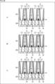
図33のAは、フォトダイオードアレイ1の半導体基板の表面側の平面図にOCLを重ねた図であり、図33のBは、図33のAのX-X線における断面図である。 FIG. 33A is a plan view of the front surface of the semiconductor substrate of the photodiode array 1 with an OCL superimposed thereon, and FIG. 33B is a cross-sectional view taken along line XX of FIG. 33A.
図33の第13実施の形態は、光の入射面が半導体基板の裏面である裏面照射型の例であり、図32に示した裏面照射型の第12実施の形態とは、OCLの構成が異なる。 The thirteenth embodiment shown in FIG. 33 is an example of a back-illuminated type in which the light incident surface is the back surface of the semiconductor substrate. different.
具体的には、図32の第12実施の形態では、1画素に対して1個のOCL101が形成されていたのに対して、図33の第13実施の形態では、1画素に対して2x2(2行2列)の4個のOCL111が形成されている。
Specifically, in the twelfth embodiment shown in FIG. 32, one
このように、1画素に対して複数のOCL111を形成する構成とすることで、入射光を、画素境界の近傍に形成される高電界領域25に集めることができる。すなわち、入射光を高電界領域25に効率的に取り込むことができるので、感度を向上させることができる。
In this way, by forming a plurality of
なお、図33は、1画素に対して4個のOCL111を配置した例であるが、1画素に対して配置するOCL111の個数および配列はこれに限られず、任意である。
Although FIG. 33 shows an example in which four
<14.第14実施の形態>
図34は、本技術を適用した光検出素子としてのフォトダイオードアレイの第14実施の形態の構成例を示している。<14. Fourteenth Embodiment>
FIG. 34 shows a configuration example of a fourteenth embodiment of a photodiode array as a photodetector to which the present technology is applied.
図34のAは、フォトダイオードアレイ1の半導体基板の表面側の平面図にOCLを重ねた図であり、図34のBは、図34のAのX-X線における断面図である。 FIG. 34A is a plan view of the front surface of the semiconductor substrate of the photodiode array 1 with OCL superimposed thereon, and FIG. 34B is a cross-sectional view taken along line XX of FIG. 34A.
図34の第14実施の形態は、光の入射面が半導体基板の裏面である裏面照射型の例であり、図32に示した裏面照射型の第12実施の形態とは、OCLの構成が異なる。 The fourteenth embodiment shown in FIG. 34 is an example of a back-illuminated type in which the light incident surface is the back surface of the semiconductor substrate. different.
具体的には、図32の第12実施の形態では、1画素に対して1個のOCL101が形成されていたのに対して、図34の第14実施の形態では、2x2の4画素に対して1個のOCL121が形成されている。
Specifically, in the twelfth embodiment shown in FIG. 32, one
このように、複数画素に対して1個のOCL121を形成する構成とすることで、高電界領域25の面積を増やすことができ、光の利用効率を向上させることができる。
Thus, by forming one
なお、フォトダイオードアレイ1を、複数画素に対して1個のOCL121を形成する構成とした場合、図35に示されるように、1個のOCL121の下方の分離部43には、金属膜42を埋め込まないことが好ましい。図34と図35は、1個のOCL121の下方の分離部43に金属膜42を有するか否かのみが異なる。2x2の4画素に対して1個のOCL121が形成される配置の場合、図34のAに示されるように、OCL121の外周を囲む2x2の矩形の分離部43には、金属膜42が埋め込まれているが、OCL121下方となる2x2の矩形の内側の分離部43には、金属膜42が省略されている。これにより、OCL121で集光された光のケラレを抑制することができる。
When the photodiode array 1 is configured such that one
図34および図35は、2x2の4画素に対して1個のOCL121を配置した例であるが、1個のOCL121を配置する画素10の個数および配列はこれに限られず、任意である。
34 and 35 are examples in which one
例えば、図36は、1x2(1行2列)の2画素に対して1個のOCL121を配置した例を示している。この場合、1個のOCL121の平面形状が略長方形となる。
For example, FIG. 36 shows an example in which one
図36においても、1個のOCL121の外周を囲む1x2画素の矩形の分離部43には、金属膜42が埋め込まれているが、OCL121下方となる1x2画素の矩形の内側の分離部43には、金属膜42が省略されている。これにより、OCL121で集光された光のケラレを抑制することができる。
36, the
また、複数画素に対して1個のOCL121を配置する場合の画素10の平面形状も、正方形以外の形状、例えば、長方形や円形でもよい。
Also, the planar shape of the
図37は、画素10の平面形状が長方形であり、長方形の画素10の2画素に対して1個のOCL121を配置した例を示している。この場合、1個のOCL121の平面形状が略正方形となる。
FIG. 37 shows an example in which the planar shape of the
図37においても、1個のOCL121の外周を囲む1x2画素の矩形の分離部43には、金属膜42が埋め込まれているが、OCL121下方となる1x2画素の矩形の内側の分離部43には、金属膜42が省略されている。これにより、OCL121で集光された光のケラレを抑制することができる。
37, the
<15.第15実施の形態>
図38は、本技術を適用した光検出素子としてのフォトダイオードアレイの第15実施の形態の構成例を示している。<15. 15th Embodiment>
FIG. 38 shows a configuration example of a fifteenth embodiment of a photodiode array as a photodetector to which the present technology is applied.
図38のAは、フォトダイオードアレイ1の半導体基板の表面側の平面図にOCLを重ねた図であり、図38のBは、図38のAのX-X線における断面図である。 FIG. 38A is a plan view of the front surface of the semiconductor substrate of the photodiode array 1 with the OCL superimposed thereon, and FIG. 38B is a cross-sectional view taken along line XX of FIG. 38A.
図38の第14実施の形態は、1画素毎に1個のOCL101が形成された裏面照射型のフォトダイオードアレイ1である図32の第12実施の形態と、半導体基板の表面側に形成された配線層102内の構成が異なる。
The fourteenth embodiment shown in FIG. 38 is a back-illuminated photodiode array 1 in which one
具体的には、図38の配線層102では、2x2の4画素で光電変換された光信号が、1画素の信号として出力されるように、2x2の4画素単位で、カソードコンタクト23どうしが接続されるとともに、アノードコンタクト24どうしが接続されている。
Specifically, in the
このように、隣接する複数画素で1つの信号出力とすることで、高感度化を図ることができる。 By outputting one signal from a plurality of adjacent pixels in this way, it is possible to achieve high sensitivity.
<16.第16実施の形態>
図39は、本技術を適用した光検出素子としてのフォトダイオードアレイの第16実施の形態の構成例を示している。<16. Sixteenth Embodiment>
FIG. 39 shows a configuration example of a sixteenth embodiment of a photodiode array as a photodetector to which the present technology is applied.
図39に示される第16実施の形態は、図17に示した第8実施の形態の構成に、読み出し回路領域を、半導体基板の表面側に追加した構成である。 The sixteenth embodiment shown in FIG. 39 has a configuration in which a readout circuit region is added to the configuration of the eighth embodiment shown in FIG. 17 on the surface side of the semiconductor substrate.
具体的には、図39の第16実施の形態では、図17に示した第8実施の形態おけるN-型第4半導体層71が拡張されており、そのN-型第4半導体層71内に、N-型第4半導体層71と反対の導電型(P型)の低い不純物濃度で、ウェル151(以下、P-型ウェル151という。)が形成されている。P-型ウェル151には、2個のソース・ドレイン領域152とゲート電極153とからなるトランジスタTr1が形成されている。2個のソース・ドレイン領域152の一方は、図中、右側のカソードコンタクト23と接続されている。図中、左側のカソードコンタクト23は、不図示のP-型ウェル151のトランジスタTr1と接続されている。
Specifically, in the sixteenth embodiment shown in FIG. 39, the N− type
このように、複数のトランジスタからなる読み出し回路領域と高電界領域25を、基板深さ方向に縦積みすることにより、読み出し回路領域と高電界領域25を平面方向に並べた構成と比較して、面積利用効率を高め、画素サイズを小さくすることができる。
In this way, by vertically stacking the readout circuit region and the high
読み出し回路領域は、複数画素で共有されてもよい。 A readout circuit region may be shared by a plurality of pixels.
図40は、読み出し回路領域が複数画素で共有される場合の構成例を示している。 FIG. 40 shows a configuration example in which a readout circuit region is shared by a plurality of pixels.
図40のAは、読み出し回路領域が複数画素で共有される場合のフォトダイオードアレイ1の半導体基板の断面図であり、図40のBは、読み出し回路領域が複数画素で共有される場合のフォトダイオードアレイ1の平面図である。図40のAの断面図は、図40のBの1点鎖線で示される部分に相当する。 FIG. 40A is a cross-sectional view of the semiconductor substrate of the photodiode array 1 when the readout circuit region is shared by a plurality of pixels, and FIG. 1 is a plan view of a diode array 1; FIG. The cross-sectional view of A in FIG. 40 corresponds to the portion indicated by the dashed line in FIG. 40B.
図40のAに示されるように、図39におけるトランジスタTr1の2個のソース・ドレイン領域152の一方が、N+型第2半導体層22に置き換えられ、N+型第2半導体層22の上面に暗電流抑制のためのピニング層171が形成されている。ピニング層171は、N+型第2半導体層22と反対の導電型であるP型の半導体層で形成される。トランジスタTr1のゲート電極153に供給される電圧を制御することによって、N+型第2半導体層22に対する信号の蓄積と読み出しが切り替えられる。
As shown in A of FIG. 40, one of the two source/
図40のBに示されるように、トランジスタTr1は、2x2(2行2列)の4画素の中央部に配置され、4画素で共有される。また、4x2(4行2列)の8画素の四隅に、アノードコンタクト24が配置され、4x2の8画素の中央部に、P-型ウェル151の電圧を制御するコンタクト172が配置される。コンタクト172には、例えば、0V等の所定の電圧が供給される。4x2の8画素の外周部には、信号読み出し用のトランジスタTr1以外の複数の制御用トランジスタTr2が配置される。
As shown in FIG. 40B, the transistor Tr1 is arranged in the center of four pixels of 2×2 (2 rows and 2 columns) and shared by the four pixels. Also, the
このように、読み出し回路領域と高電界領域25を基板深さ方向に縦積みする構成において、読み出し回路領域を複数画素で共有することで、さらに面積利用効率を高め、画素サイズを小さくすることができる。
In this way, in the configuration in which the readout circuit region and the high
<17.第1の製造方法>
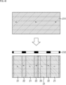
次に、図41を参照して、フォトダイオードアレイ1の半導体基板に、P+型第1半導体層21およびN+型第2半導体層22を形成する第1の製造方法について説明する。この第1の製造方法は、例えば、図1および図2に示した第1実施の形態に適用することができる。<17. First Manufacturing Method>
Next, referring to FIG. 41, a first manufacturing method for forming the P + -type
初めに、リン(P)等のN型不純物のイオン注入を半導体基板の深さ方向に複数回行うことにより、N+型のウェル211(以下、N+型ウェル211という。)が形成される。 First, an N+ type well 211 (hereinafter referred to as an N+ type well 211) is formed by ion-implanting an N-type impurity such as phosphorus (P) a plurality of times in the depth direction of the semiconductor substrate.
次に、P+型第1半導体層21の形成領域に合わせてパターニングされたマスク212を用いて、ボロン(B)等のP型不純物のイオン注入を半導体基板の深さ方向に複数回行うことにより、P+型第1半導体層21が形成される。P+型第1半導体層21が形成される領域は、例えば、図1のAの平面図のように、画素10の境界およびその近傍の外周部に相当する。形成されたP+型第1半導体層21以外のN+型ウェル211の領域が、N+型第2半導体層22となる。以上により、半導体基板の深さ方向に高電界領域25を形成することができる。
Next, using a
半導体基板の深さ方向にイオン注入を複数回行うことにより、N+型ウェル211およびP+型第1半導体層21を形成する方法では、図41において濃淡で示されるように、N+型ウェル211およびP+型第1半導体層21の各領域において深さ方向に濃度差が発生するが、N+型ウェル211の不純物濃度は、例えば1015乃至1017/cm3程度に制御されることが好ましい。また、P+型第1半導体層21の不純物濃度としては、N+型ウェル211の不純物濃度よりも高い濃度が好ましい。In the method of forming the N+ type well 211 and the P+ type
その後、裏面側界面の全領域にP型不純物がイオン注入されることにより、裏面側界面の全領域にP+型第1半導体層21が形成される。なお、P型不純物のイオン注入は、裏面側界面の全領域ではなく、マスクを用いて、N+型第2半導体層22の領域のみでもよい。あるいはまた、図2に示したように、裏面側界面に暗電流抑制のための固定電荷膜28を形成する場合には、固定電荷膜28に正孔が蓄積されるため、裏面側界面の全領域をP+型第1半導体層21とせずに、固定電荷膜28を追加形成してもよい。
After that, a P+ type
次に、半導体基板の表面側界面に、カソードコンタクト23およびアノードコンタクト24が形成される。
Next, a
以上のようにして、P+型第1半導体層21およびN+型第2半導体層22を形成することができる。
As described above, the P + -type
<18.第2の製造方法>
次に、図42を参照して、フォトダイオードアレイ1の半導体基板に、P+型第1半導体層21およびN+型第2半導体層22を形成する第2の製造方法について説明する。この第2の製造方法は、図3の第2実施の形態のように、画素10の境界に、分離部43を設ける場合に適用できる。<18. Second Manufacturing Method>
Next, a second manufacturing method for forming the P + -type
初めに、リン(P)等のN型不純物のイオン注入を半導体基板の深さ方向に複数回行うことにより、N+型のウェル221(以下、N+型ウェル221という。)が形成される。 First, an N+ type well 221 (hereinafter referred to as an N+ type well 221) is formed by ion-implanting an N-type impurity such as phosphorus (P) a plurality of times in the depth direction of the semiconductor substrate.
次に、N+型ウェル221内の画素10の境界およびその近傍の外周部に相当する領域の基板深さ方向に、P型のイオンを含む酸化膜222が埋め込まれ、熱拡散によってP+型第1半導体層21が形成される。形成されたP+型第1半導体層21以外のN+型ウェル221の領域が、N+型第2半導体層22となる。以上により、半導体基板の深さ方向に高電界領域25を形成することができる。
Next, an
N+型ウェル221の不純物濃度は、例えば1015乃至1017/cm3程度に制御されることが好ましい。また、P+型第1半導体層21の不純物濃度としては、N+型ウェル221の不純物濃度よりも高い濃度が好ましい。熱拡散によって形成されたP+型第1半導体層21は、基板深さ方向に直交する横方向に、キャリア移動に影響のない範囲内で濃度差が発生してもよい。The impurity concentration of the N+ type well 221 is preferably controlled to, for example, approximately 10 15 to 10 17 /cm 3 . Moreover, the impurity concentration of the P + -type
その後の工程は、図41を参照して説明した第1の製造方法と同様である。 Subsequent steps are the same as those of the first manufacturing method described with reference to FIG.
すなわち、裏面側界面の全領域、または、N+型第2半導体層22の領域のみに、P型不純物がイオン注入され、裏面側界面の全領域にP+型第1半導体層21が形成される。あるいはまた、裏面側界面の全領域をP+型第1半導体層21とする工程は省略されて、裏面界面に固定電荷膜28が形成される。そして、半導体基板の表面側界面に、カソードコンタクト23およびアノードコンタクト24が形成される。
That is, a P-type impurity is ion-implanted into the entire region of the back-side interface or only the region of the N+-type
酸化膜222は、分離部43を構成する絶縁膜41としてそのまま残される。分離部43として絶縁膜41の内側に金属膜42を設ける場合には、さらに、絶縁膜41としての酸化膜222の一部を開口して、金属材料が埋め込まれる。
The
<19.第3の製造方法>
次に、図43を参照して、フォトダイオードアレイ1の半導体基板に、P+型第1半導体層21およびN+型第2半導体層22を形成する第3の製造方法について説明する。この第3の製造方法も、画素10の境界に、分離部43を設ける場合の製造方法である。<19. Third Manufacturing Method>
Next, a third manufacturing method for forming the P + -type
図42で説明した第2の製造方法では、最初に、リン(P)等のN型不純物のイオン注入を半導体基板の深さ方向に複数回行うことにより、N+型ウェル221を形成した。第3の製造方法では、半導体基板にN+型ウェル221を形成する代わりに、高濃度のN型(N+)の半導体基板231が用いられる。それ以外の方法は、図41で説明した第2の製造方法と同様である。
In the second manufacturing method described with reference to FIG. 42, first, an N+ type well 221 is formed by ion-implanting an N-type impurity such as phosphorus (P) a plurality of times in the depth direction of the semiconductor substrate. In the third manufacturing method, a high-concentration N-type (N+)
N+型の半導体基板231の不純物濃度は、例えば1015乃至1017/cm3程度に制御されることが好ましく、P+型第1半導体層21の不純物濃度としては、N+型の半導体基板231の不純物濃度よりも高い濃度が好ましい。熱拡散によって形成されたP+型第1半導体層21は、基板深さ方向に直交する横方向に、キャリア移動に影響のない範囲内で濃度差が発生する。The impurity concentration of the N+
その後の工程は、図41で説明した第1の製造方法と同様である。 Subsequent steps are the same as those of the first manufacturing method described with reference to FIG.
<20.第4の製造方法>
次に、図44を参照して、フォトダイオードアレイ1の半導体基板に、P+型第1半導体層21およびN+型第2半導体層22を形成する第4の製造方法について説明する。この第4の製造方法も、画素10の境界に、分離部43を設ける場合の製造方法である。<20. Fourth Manufacturing Method>
Next, a fourth manufacturing method for forming the P + -type
初めに、半導体基板261に対して、画素10の境界およびその近傍の外周部に相当する領域の基板深さ方向に、N型のイオンを含む第1酸化膜262が埋め込まれ、熱拡散によってN+型の半導体層263が形成される。
First, a
次に、形成されたN型のイオンを含む第1酸化膜262が除去され、その除去された部分に、P型のイオンを含む第2酸化膜264が埋め込まれ、熱拡散によってP+型の半導体層21が形成される。形成されたP+型第1半導体層21以外のN+型の半導体層263の領域が、N+型第2半導体層22となる。以上により、半導体基板の深さ方向に高電界領域25を形成することができる。
Next, the formed
N+型第2半導体層22の不純物濃度は、例えば1015乃至1017/cm3程度に制御されることが好ましく、P+型第1半導体層21の不純物濃度としては、N+型第2半導体層22の不純物濃度よりも高い濃度が好ましい。熱拡散によって形成されたP+型第1半導体層21およびN+型第2半導体層22は、基板深さ方向に直交する横方向に、キャリア移動に影響のない範囲内で濃度差が発生してもよい。The impurity concentration of the N + -type
その後の工程は、図41で説明した第1の製造方法と同様である。 Subsequent steps are the same as those of the first manufacturing method described with reference to FIG.
<21.第5の製造方法>
次に、図45を参照して、フォトダイオードアレイ1の半導体基板に、P+型第1半導体層21およびN+型第2半導体層22を形成する第5の製造方法について説明する。この第5の製造方法も、画素10の境界に、分離部43を設ける場合の製造方法である。<21. Fifth Manufacturing Method>
Next, a fifth manufacturing method for forming the P + -type
初めに、半導体基板261に対して、画素10の境界およびその近傍の外周部に相当する領域の基板深さ方向に、N型のイオンを含む第1酸化膜262が埋め込まれる。
First, a
次に、半導体基板261に対して、画素10の境界およびその近傍の外周部に相当する領域の基板深さ方向に、P型のイオンを含む第2酸化膜264が埋め込まれる。P型のイオンを含む第2酸化膜264が埋め込まれる領域は、N型のイオンを含む第1酸化膜262を埋め込んだ領域と異なる領域であり、N型のイオンを含む第1酸化膜262が埋め込まれた領域と、P型のイオンを含む第2酸化膜264が埋め込まれた領域のそれぞれが、分離部43の絶縁膜41の領域に対応する。
Next, a
次に、熱拡散を行うことにより、P+型の半導体層21とN+型第2半導体層22が形成される。以上により、半導体基板の深さ方向に高電界領域25を形成することができる。
Next, a P+
N+型第2半導体層22の不純物濃度は、好ましくは例えば1015乃至1017/cm3程度に制御され、P+型第1半導体層21の不純物濃度としては、N+型第2半導体層22の不純物濃度よりも高い濃度が好ましい。熱拡散によって形成されたP+型第1半導体層21およびN+型第2半導体層22は、基板深さ方向に直交する横方向に、キャリア移動に影響のない範囲内で濃度差が発生してもよい。The impurity concentration of the N + -type
その後の工程は、図41で説明した第1の製造方法と同様である。 Subsequent steps are the same as those of the first manufacturing method described with reference to FIG.
<22.第6の製造方法>
次に、図46を参照して、フォトダイオードアレイ1の半導体基板に、P+型第1半導体層21およびN+型第2半導体層22を形成する第6の製造方法について説明する。この第6の製造方法は、図9に示した第4実施の形態のように、テーパ形状の分離部43を基板表面側から掘り込んで形成する場合の製造方法である。<22. Sixth Manufacturing Method>
Next, a sixth manufacturing method for forming the P + -type
初めに、図46のAに示されるように、低濃度のN型(N-)の半導体基板281の表面側から所定の深さで掘り込むことにより、トレンチ282が形成される。トレンチ282は、表面側の開口面積が広く、底部となる裏面側の開口面積が狭いテーパ形状で作製される。
First, as shown in FIG. 46A, a
次に、図46のBに示されるように、トレンチ282の側面から、リン(P)等のN型不純物のイオン注入を行うことにより、N+型第2半導体層22が、トレンチ282の側面に沿って形成される。
Next, as shown in FIG. 46B, N-type impurity ions such as phosphorus (P) are implanted from the side surfaces of the
次に、図46のCに示されるように、トレンチ282の側面から、N+型第2半導体層22よりも浅い基板内に、ボロン(B)等のP型不純物のイオン注入を行うことにより、P+型第1半導体層21が形成される。イオン注入には、例えば、プラズマドーピングによって浅く打ち込むことで、電界をより付けやすくすることができる。
Next, as shown in FIG. 46C, P-type impurity ions such as boron (B) are implanted from the side surface of the
次に、図46のDに示されるように、トレンチ282の内部に、酸化膜41を埋め込むことにより、分離部43が形成される。分離部43として金属膜42も設ける場合には、酸化膜41を埋め込んだ後に、酸化膜41の一部を開口して、金属膜42が埋め込まれる。
Next, as shown in FIG. 46D, an
その後の工程は、図41で説明した第1の製造方法と同様である。 Subsequent steps are the same as those of the first manufacturing method described with reference to FIG.
<23.第7の製造方法>
次に、図47および図48を参照して、フォトダイオードアレイ1の半導体基板に、P+型第1半導体層21およびN+型第2半導体層22を形成する第7の製造方法について説明する。この第7の製造方法は、図24に示した第9実施の形態のように、テーパ形状の分離部43を基板裏面側から掘り込んで形成する場合の製造方法である。<23. Seventh Manufacturing Method>
Next, a seventh manufacturing method for forming the P + -type
テーパ形状の分離部43を基板裏面側から掘り込んで形成する場合、例えば、図47のAに示されるように、低濃度のN型(N-)の半導体基板301の表面側に、カソードコンタクト23、アノードコンタクト24、アノードコンタクト24の周囲のP-型第6半導体層81などが、最初に形成される。その後、カソードコンタクト23およびアノードコンタクト24等が形成された基板表面上に、配線層302が形成される。
When forming the tapered
配線層302を形成した後、図47のBに示されるように、半導体基板301の上下が反転され、半導体基板301の裏面側から、所定の深さでトレンチ311が形成される。
After the
次に、図47のCに示されるように、トレンチ311の側面から、リン(P)等のN型不純物のイオン注入を行うことにより、N+型第2半導体層22が形成される。
Next, as shown in FIG. 47C, N+ type
次に、図48のAに示されるように、トレンチ311の側面から、N+型第2半導体層22よりも浅い基板内に、ボロン(B)等のP型不純物のイオン注入を行うことにより、P+型第1半導体層21が形成される。イオン注入には、例えば、プラズマドーピングによって浅く打ち込むことで、電界をより付けやすくすることができる。
Next, as shown in FIG. 48A, by ion-implanting a P-type impurity such as boron (B) from the side surface of the
次に、図48のBに示されるように、トレンチ311の側面および底面と、トレンチ311が形成されていない半導体基板301の裏面界面に、固定電荷膜29が形成される。この固定電荷膜29は、例えば、HfO2、Al2O3等の膜とされる。
Next, as shown in FIG. 48B, a fixed
次に、図48のCに示されるように、トレンチ311の内部に、酸化膜41が埋め込まれ、分離部43が形成される。分離部43として金属膜42も設ける場合には、酸化膜41を埋め込んだ後に、酸化膜41の一部を開口して、金属膜42が埋め込まれる。
Next, as shown in FIG. 48C, the
以上のようにして、基板裏面側から形成したテーパ形状の分離部43を有するフォトダイオードアレイ1を製造することができる。
As described above, the photodiode array 1 having the tapered separating
<24.まとめ>
以上説明したように、第1乃至第16実施の形態に係るフォトダイオードアレイ1は、マトリクス状に配置された複数の画素10を備え、画素境界近傍の外周部に形成された第1導電型(例えば、P型)の第1半導体層(P+型第1半導体層21)と、平面視において第1半導体層の内側に形成された、第1導電型と反対の第2導電型(例えば、N型)の第2半導体層(N+型第2半導体層22)とを備え、逆バイアス電圧が印加されたときに第1半導体層と第2半導体層とで形成される高電界領域25が基板の深さ方向に形成されるように構成される。<24. Summary>
As described above, the photodiode array 1 according to the first to sixteenth embodiments includes a plurality of
基板深さ方向(縦方向)に高電界領域25を形成するため、ガードリングを設けずに、平面方向に小面積で高電界領域25を形成することができるので、画素サイズを小さくすることができる。
Since the high
さらに、フォトダイオードアレイ1において、画素境界に分離部43を形成した場合には、電気的及び光学的なクロストークを低減することができる。
Furthermore, in the photodiode array 1, if the separating
高電界領域25が基板の深さ方向に形成される第1導電型(例えば、P型)の第1半導体層(P+型第1半導体層21)と、第2導電型(例えば、N型)の第2半導体層(N+型第2半導体層22)は、上述した第1乃至第7の製造方法のいずれかを用いて形成することができる。
A first conductivity type (for example, P type) first semiconductor layer (P+ type first semiconductor layer 21) in which a high
基板深さ方向(縦方向)に高電界領域25を形成可能なAPDをマトリクス状に配置したフォトダイオードアレイ1は、例えば、フォトンカウンタや、TOF(Time of Flight)センサの受光素子に用いることができる。
A photodiode array 1 in which APDs capable of forming a high
本技術の実施の形態は、上述した実施の形態に限定されるものではなく、本技術の要旨を逸脱しない範囲において種々の変更が可能である。 Embodiments of the present technology are not limited to the above-described embodiments, and various modifications are possible without departing from the gist of the present technology.
例えば、上述した複数の実施の形態の全てまたは一部を組み合わせた形態を採用することができる。 For example, a form obtained by combining all or part of the multiple embodiments described above can be adopted.
なお、本明細書に記載された効果はあくまで例示であって限定されるものではなく、本明細書に記載されたもの以外の効果があってもよい。 Note that the effects described in this specification are merely examples and are not limited, and there may be effects other than those described in this specification.
なお、本技術は以下のような構成も取ることができる。
(1)
マトリクス状に配置された複数の画素を備え、
前記画素は、
画素境界近傍の外周部に形成された第1導電型の第1半導体層と、
平面視において前記第1半導体層の内側に形成された、前記第1導電型と反対の第2導電型の第2半導体層と
を備え、
逆バイアス電圧が印加されたときに前記第1半導体層と前記第2半導体層とで形成される高電界領域が、基板の深さ方向に形成されるように構成された
光検出素子。
(2)
画素境界に、隣接する画素間を絶縁分離する分離部をさらに備え、
前記高電界領域は、前記分離部に隣接して形成されるように構成された
前記(1)に記載の光検出素子。
(3)
平面視において前記第2半導体層の内側に、前記第2半導体層よりも不純物濃度が低い前記第2導電型の第3半導体層をさらに備える
前記(1)または(2)に記載の光検出素子。
(4)
前記第2半導体層は、前記基板の表面に向かって不純物濃度が濃くなる電位勾配を有する
前記(1)乃至(3)のいずれかに記載の光検出素子。
(5)
前記第2半導体層の前記基板の深さ方向に隣接して、不純物濃度が低い前記第1導電型または前記第2導電型の第4半導体層をさらに備える
前記(1)乃至(4)のいずれかに記載の光検出素子。
(6)
前記第4半導体層は、前記第2半導体層に対して前記基板の表面側に隣接し、前記第2導電型である
前記(5)に記載の光検出素子。
(7)
前記第4半導体層は、前記第2半導体層に対して前記基板の裏面側に隣接し、前記第2導電型である
前記(5)または(6)に記載の光検出素子。
(8)
前記第4半導体層は、前記第2半導体層に対して前記基板の表面側に隣接し、前記第1導電型である
前記(5)に記載の光検出素子。
(9)
前記第4半導体層は、前記第2半導体層に対して前記基板の裏面側に隣接し、前記第1導電型である
前記(5)または(8)に記載の光検出素子。
(10)
前記基板の表面に形成された前記第1導電型のウェル内に、読み出し回路をさらに備える
前記(1)乃至(9)のいずれかに記載の光検出素子。
(11)
前記読み出し回路は、複数の画素で共有される
前記(10)に記載の光検出素子。
(12)
前記第2半導体層に隣接し、かつ、前記基板の表面に、前記第1導電型の第5半導体層をさらに備える
前記(10)または(11)に記載の光検出素子。
(13)
前記読み出し回路は、ゲート電極を制御することによって、信号の蓄積と読み出しを切り替える
前記(10)乃至(12)のいずれかに記載の光検出素子。
(14)
マトリクス状に配置される画素の境界近傍の外周部に、第1導電型の第1半導体層を形成し、
平面視において前記第1半導体層の内側に、前記第1導電型と反対の第2導電型の第2半導体層を形成し、
逆バイアス電圧が印加されたときに前記第1半導体層と前記第2半導体層とで形成される高電界領域が、基板の深さ方向に形成されるように構成された
光検出素子の製造方法。
(15)
前記第2導電型のウェル内の前記画素の境界近傍の外周部に、第1導電型のイオン注入を行うことによって、前記外周部の前記第1半導体層と、その内側の前記第2半導体層とを形成する
前記(14)に記載の光検出素子の製造方法。
(16)
前記第2導電型のウェルは、前記基板にイオン注入を行うことによって形成される
前記(15)に記載の光検出素子の製造方法。
(17)
前記第2導電型のウェルとして、前記第2導電型の前記基板が用いられる
前記(15)に記載の光検出素子の製造方法。
(18)
前記第2導電型のイオンを含んだ第1酸化膜を埋め込み、熱拡散によって前記第2半導体層を形成した後、前記第1酸化膜を除去して、その除去された部分に、前記第1導電型のイオンを含んだ第2酸化膜を埋め込み、熱拡散によって前記第1半導体層を形成することによって、前記外周部の前記第1半導体層と、その内側の前記第2半導体層とを形成する
前記(15)に記載の光検出素子の製造方法。
(19)
前記第1導電型のイオンを含んだ第1酸化膜を埋め込み、前記第2導電型のイオンを含んだ第2酸化膜を前記第1酸化膜とは別の領域に埋め込み、熱拡散によって前記第1半導体層と前記第2半導体層を形成することによって、前記外周部の前記第1半導体層と、その内側の前記第2半導体層とを形成する
前記(15)に記載の光検出素子の製造方法。
(20)
前記基板の前記画素の境界に、前記基板の所定の深さまで掘り込んだトレンチを形成し、前記トレンチの側面から前記第1導電型のイオン注入と前記第2導電型のイオン注入を行うことで、前記外周部の前記第1半導体層と、その内側の前記第2半導体層とを形成する
前記(15)に記載の光検出素子の製造方法。Note that the present technology can also take the following configuration.
(1)
Equipped with a plurality of pixels arranged in a matrix,
The pixels are
a first conductivity type first semiconductor layer formed in an outer peripheral portion near a pixel boundary;
a second semiconductor layer of a second conductivity type opposite to the first conductivity type formed inside the first semiconductor layer in plan view,
A photodetector element configured such that a high electric field region formed by the first semiconductor layer and the second semiconductor layer is formed in the depth direction of the substrate when a reverse bias voltage is applied.
(2)
further comprising a separation section for insulating and separating adjacent pixels at a pixel boundary;
The photodetector according to (1), wherein the high electric field region is formed adjacent to the isolation section.
(3)
The photodetector according to (1) or (2), further comprising a third semiconductor layer of the second conductivity type having an impurity concentration lower than that of the second semiconductor layer inside the second semiconductor layer in plan view. .
(4)
The photodetector according to any one of (1) to (3), wherein the second semiconductor layer has a potential gradient in which the impurity concentration increases toward the surface of the substrate.
(5)
Any one of (1) to (4) above, further comprising a fourth semiconductor layer of the first conductivity type or the second conductivity type with a low impurity concentration adjacent to the second semiconductor layer in the depth direction of the substrate. The photodetector according to 1.
(6)
The photodetector according to (5), wherein the fourth semiconductor layer is adjacent to the second semiconductor layer on the surface side of the substrate and is of the second conductivity type.
(7)
The photodetector according to (5) or (6), wherein the fourth semiconductor layer is adjacent to the second semiconductor layer on the back surface side of the substrate and is of the second conductivity type.
(8)
The photodetector according to (5), wherein the fourth semiconductor layer is adjacent to the second semiconductor layer on the surface side of the substrate and is of the first conductivity type.
(9)
The photodetector according to (5) or (8), wherein the fourth semiconductor layer is adjacent to the second semiconductor layer on the back surface side of the substrate and is of the first conductivity type.
(10)
The photodetector according to any one of (1) to (9), further comprising a readout circuit in the first conductivity type well formed on the surface of the substrate.
(11)
The photodetector according to (10), wherein the readout circuit is shared by a plurality of pixels.
(12)
The photodetector according to (10) or (11), further comprising a fifth semiconductor layer of the first conductivity type adjacent to the second semiconductor layer and on the surface of the substrate.
(13)
The photodetector according to any one of (10) to (12), wherein the readout circuit switches between signal accumulation and readout by controlling a gate electrode.
(14)
forming a first semiconductor layer of a first conductivity type on an outer peripheral portion near a boundary of pixels arranged in a matrix;
forming a second semiconductor layer of a second conductivity type opposite to the first conductivity type inside the first semiconductor layer in plan view;
A method for manufacturing a photodetector, wherein a high electric field region formed by the first semiconductor layer and the second semiconductor layer is formed in the depth direction of the substrate when a reverse bias voltage is applied. .
(15)
By performing ion implantation of the first conductivity type in the outer peripheral portion near the boundary of the pixel in the well of the second conductivity type, the first semiconductor layer in the outer peripheral portion and the second semiconductor layer inside thereof are formed. The method for manufacturing the photodetector element according to (14) above.
(16)
The method of manufacturing a photodetector element according to (15), wherein the well of the second conductivity type is formed by implanting ions into the substrate.
(17)
The method for manufacturing a photodetector element according to (15), wherein the substrate of the second conductivity type is used as the well of the second conductivity type.
(18)
After embedding the first oxide film containing ions of the second conductivity type and forming the second semiconductor layer by thermal diffusion, the first oxide film is removed, and the first oxide film is formed in the removed portion. By embedding a second oxide film containing ions of a conductive type and forming the first semiconductor layer by thermal diffusion, the first semiconductor layer on the outer peripheral portion and the second semiconductor layer on the inside thereof are formed. The method for manufacturing the photodetector according to (15) above.
(19)
A first oxide film containing ions of the first conductivity type is buried, a second oxide film containing ions of the second conductivity type is buried in a region different from the first oxide film, and the second oxide film is buried by thermal diffusion. Manufacture of the photodetector according to (15) above, wherein the first semiconductor layer in the outer peripheral portion and the second semiconductor layer inside thereof are formed by forming one semiconductor layer and the second semiconductor layer. Method.
(20)
forming a trench at a boundary of the pixel on the substrate by digging the substrate to a predetermined depth, and performing ion implantation of the first conductivity type and ion implantation of the second conductivity type from the side surface of the trench; and forming the first semiconductor layer on the outer peripheral portion and the second semiconductor layer on the inner side thereof.
1 フォトダイオードアレイ, 10 画素, 21 第1半導体層(P+型第1半導体層), 22 第2半導体層(N+型第2半導体層), 23 コンタクト(カソードコンタクト), 24 コンタクト(アノードコンタクト), 25 高電界領域, 28,29 固定電荷膜, 41 酸化膜, 42 金属膜, 43 分離部, 61 第3半導体層(N-型第3半導体層), 71 第4半導体層(N-型第4半導体層), 72 第5半導体層(N-型第5半導体層), 81 第6半導体層(P-型第6半導体層), 82 第7半導体層(P-型第7半導体層), 83 第8半導体層(N-型第9半導体層), 91 第10半導体層(N-型第10半導体層), 151 ウェル(P-型ウェル), 153 ゲート電極, 171 ピニング層, 172 コンタクト, 211 ウェル(N+型ウェル), 221 ウェル(N+型ウェル), 222 酸化膜, 231,261 半導体基板, 262 第1酸化膜, 263 半導体層, 264 第2酸化膜, 281 半導体基板, 282,311 トレンチ
1 photodiode array, 10 pixels, 21 first semiconductor layer (P+ type first semiconductor layer), 22 second semiconductor layer (N+ type second semiconductor layer), 23 contact (cathode contact), 24 contact (anode contact), 25 high
Claims (15)
前記画素は、
画素境界近傍の外周部に形成された第1導電型の第1半導体層と、
平面視において前記第1半導体層の内側に前記第1半導体層と接触して形成された、前記第1導電型と反対の第2導電型の第2半導体層と、
平面視において前記第2半導体層の内側に前記第2半導体層と接触して形成された、前記第2半導体層よりも不純物濃度が低い前記第2導電型の第3半導体層と
を備え、
逆バイアス電圧が印加されたときに前記第1半導体層と前記第2半導体層とで形成される高電界領域が、断面視で基板の深さ方向に縦長に形成されるように構成された
光検出素子。 Equipped with a plurality of pixels arranged in a matrix,
The pixels are
a first conductivity type first semiconductor layer formed in an outer peripheral portion near a pixel boundary;
a second semiconductor layer of a second conductivity type opposite to the first conductivity type formed inside the first semiconductor layer in plan view and in contact with the first semiconductor layer;
a third semiconductor layer of the second conductivity type formed in contact with the second semiconductor layer inside the second semiconductor layer in plan view and having an impurity concentration lower than that of the second semiconductor layer;
Light configured such that a high electric field region formed by the first semiconductor layer and the second semiconductor layer is formed vertically in the depth direction of the substrate in a cross-sectional view when a reverse bias voltage is applied. detection element.
前記画素は、
画素境界近傍の外周部に形成された第1導電型の第1半導体層と、
平面視において前記第1半導体層の内側に前記第1半導体層と接触して形成された、前記第1導電型と反対の第2導電型の第2半導体層と
を備え、
前記第2半導体層は、基板の表面に向かって不純物濃度が濃くなる電位勾配を有し、
逆バイアス電圧が印加されたときに前記第1半導体層と前記第2半導体層とで形成される高電界領域が、断面視で前記基板の深さ方向に縦長に形成されるように構成された
光検出素子。 Equipped with a plurality of pixels arranged in a matrix,
The pixels are
a first conductivity type first semiconductor layer formed in an outer peripheral portion near a pixel boundary;
a second semiconductor layer of a second conductivity type opposite to the first conductivity type formed in contact with the first semiconductor layer inside the first semiconductor layer in plan view,
the second semiconductor layer has a potential gradient in which the impurity concentration increases toward the surface of the substrate;
A high electric field region formed by the first semiconductor layer and the second semiconductor layer when a reverse bias voltage is applied is configured to be vertically long in a depth direction of the substrate in a cross-sectional view. Photodetector.
前記高電界領域は、前記分離部に隣接して形成されるように構成された
請求項1または2に記載の光検出素子。 further comprising a separation section for insulating and separating adjacent pixels at a pixel boundary;
3. The photodetector element according to claim 1, wherein the high electric field region is formed adjacent to the isolation section.
請求項1または2に記載の光検出素子。 3. The photodetector according to claim 1, further comprising a fourth semiconductor layer of the first conductivity type or the second conductivity type having a low impurity concentration adjacent to the second semiconductor layer in the depth direction of the substrate. element.
請求項4に記載の光検出素子。 5. The photodetector according to claim 4, wherein the fourth semiconductor layer is adjacent to the second semiconductor layer on the surface side of the substrate and is of either the first conductivity type or the second conductivity type.
請求項4に記載の光検出素子。 5. The photodetector according to claim 4, wherein the fourth semiconductor layer is adjacent to the second semiconductor layer on the back side of the substrate and is of either the first conductivity type or the second conductivity type.
請求項3に記載の光検出素子。 4. The photodetector according to claim 3 , wherein the separating portion has a tapered shape when viewed in cross section .
請求項1乃至7のいずれかに記載の光検出素子。 8. The photodetector according to any one of claims 1 to 7, wherein the distance in the planar direction of the high electric field regions facing each other in the pixel is different between the front surface side and the rear surface side of the substrate .
請求項1または2に記載の光検出素子。 3. The photodetector according to claim 1, further comprising a readout circuit in the well of the first conductivity type formed on the surface of the substrate.
請求項9に記載の光検出素子。 10. The photodetector according to claim 9, wherein the readout circuit is shared by a plurality of pixels.
請求項9に記載の光検出素子。 10. The photodetector according to claim 9, further comprising a fifth semiconductor layer of the first conductivity type adjacent to the second semiconductor layer and on the surface of the substrate.
請求項11に記載の光検出素子。 12. The photodetector according to claim 11, wherein the readout circuit switches between signal accumulation and readout by controlling a gate electrode.
平面視において前記第1半導体層の内側に、前記第1導電型と反対の第2導電型の第2半導体層を形成し、
前記第2導電型のイオンを含んだ第1酸化膜を埋め込み、熱拡散によって前記第2半導体層を形成した後、前記第1酸化膜を除去して、その除去された部分に、前記第1導電型のイオンを含んだ第2酸化膜を埋め込み、熱拡散によって前記第1半導体層を形成することによって、前記外周部の前記第1半導体層と、その内側の前記第2半導体層とが形成され、
逆バイアス電圧が印加されたときに前記第1半導体層と前記第2半導体層とで形成される高電界領域が、基板の深さ方向に形成されるように構成された
光検出素子の製造方法。 forming a first semiconductor layer of a first conductivity type on an outer peripheral portion near a boundary of pixels arranged in a matrix;
forming a second semiconductor layer of a second conductivity type opposite to the first conductivity type inside the first semiconductor layer in plan view;
After embedding the first oxide film containing ions of the second conductivity type and forming the second semiconductor layer by thermal diffusion, the first oxide film is removed, and the first oxide film is formed in the removed portion. By embedding a second oxide film containing ions of a conductive type and forming the first semiconductor layer by thermal diffusion, the first semiconductor layer on the outer peripheral portion and the second semiconductor layer on the inside thereof are formed. is,
A method for manufacturing a photodetector, wherein a high electric field region formed by the first semiconductor layer and the second semiconductor layer is formed in the depth direction of the substrate when a reverse bias voltage is applied. .
平面視において前記第1半導体層の内側に、前記第1導電型と反対の第2導電型の第2半導体層を形成し、
前記第1導電型のイオンを含んだ第1酸化膜を埋め込み、前記第2導電型のイオンを含んだ第2酸化膜を前記第1酸化膜とは別の領域に埋め込み、熱拡散によって前記第1半導体層と前記第2半導体層を形成することによって、前記外周部の前記第1半導体層と、その内側の前記第2半導体層とが形成され、
逆バイアス電圧が印加されたときに前記第1半導体層と前記第2半導体層とで形成される高電界領域が、基板の深さ方向に形成されるように構成された
光検出素子の製造方法。 forming a first semiconductor layer of a first conductivity type on an outer peripheral portion near a boundary of pixels arranged in a matrix;
forming a second semiconductor layer of a second conductivity type opposite to the first conductivity type inside the first semiconductor layer in plan view;
A first oxide film containing ions of the first conductivity type is buried, a second oxide film containing ions of the second conductivity type is buried in a region different from the first oxide film, and the second oxide film is buried by thermal diffusion. By forming one semiconductor layer and the second semiconductor layer, the first semiconductor layer in the outer peripheral portion and the second semiconductor layer inside thereof are formed,
A method for manufacturing a photodetector, wherein a high electric field region formed by the first semiconductor layer and the second semiconductor layer is formed in the depth direction of the substrate when a reverse bias voltage is applied. .
平面視において前記第1半導体層の内側に、前記第1導電型と反対の第2導電型の第2半導体層を形成し、
基板の前記画素の境界に、前記基板の所定の深さまで掘り込んだトレンチを形成し、前記トレンチの側面から前記第1導電型のイオン注入と前記第2導電型のイオン注入を行うことで、前記外周部の前記第1半導体層と、その内側の前記第2半導体層とが形成され、
逆バイアス電圧が印加されたときに前記第1半導体層と前記第2半導体層とで形成される高電界領域が、前記基板の深さ方向に形成されるように構成された
光検出素子の製造方法。 forming a first semiconductor layer of a first conductivity type on an outer peripheral portion near a boundary of pixels arranged in a matrix;
forming a second semiconductor layer of a second conductivity type opposite to the first conductivity type inside the first semiconductor layer in plan view;
By forming a trench that is dug to a predetermined depth in the substrate at the boundary of the pixel on the substrate, and performing the ion implantation of the first conductivity type and the ion implantation of the second conductivity type from the side surface of the trench, The first semiconductor layer in the outer peripheral portion and the second semiconductor layer inside thereof are formed,
Manufacture of a photodetector configured such that a high electric field region formed by the first semiconductor layer and the second semiconductor layer is formed in the depth direction of the substrate when a reverse bias voltage is applied. Method.
Applications Claiming Priority (3)
| Application Number | Priority Date | Filing Date | Title |
|---|---|---|---|
| JP2017219685 | 2017-11-15 | ||
| JP2017219685 | 2017-11-15 | ||
| PCT/JP2018/040660 WO2019098035A1 (en) | 2017-11-15 | 2018-11-01 | Photodetection element and method for manufacturing same |
Publications (2)
| Publication Number | Publication Date |
|---|---|
| JPWO2019098035A1 JPWO2019098035A1 (en) | 2020-10-01 |
| JP7242527B2 true JP7242527B2 (en) | 2023-03-20 |
Family
ID=66540222
Family Applications (1)
| Application Number | Title | Priority Date | Filing Date |
|---|---|---|---|
| JP2019527577A Active JP7242527B2 (en) | 2017-11-15 | 2018-11-01 | Photodetector and manufacturing method thereof |
Country Status (7)
| Country | Link |
|---|---|
| US (2) | US11264420B2 (en) |
| EP (1) | EP3553824B1 (en) |
| JP (1) | JP7242527B2 (en) |
| KR (2) | KR102615816B1 (en) |
| CN (1) | CN110050348B (en) |
| DE (1) | DE112018005850T5 (en) |
| WO (1) | WO2019098035A1 (en) |
Families Citing this family (11)
| Publication number | Priority date | Publication date | Assignee | Title |
|---|---|---|---|---|
| EP3553824B1 (en) | 2017-11-15 | 2022-07-20 | Sony Semiconductor Solutions Corporation | Photodetection element and method for manufacturing same |
| TW202125795A (en) * | 2019-11-19 | 2021-07-01 | 日商索尼半導體解決方案公司 | Solid-state imaging device and electronic apparatus |
| JP2021114538A (en) * | 2020-01-20 | 2021-08-05 | ソニーセミコンダクタソリューションズ株式会社 | Imaging element and imaging device |
| US11508867B2 (en) * | 2020-01-28 | 2022-11-22 | Adaps Photonics Inc. | Single photon avalanche diode device |
| TW202137523A (en) * | 2020-03-16 | 2021-10-01 | 日商索尼半導體解決方案公司 | Light-receiving element and ranging system |
| US11621287B2 (en) * | 2020-04-16 | 2023-04-04 | Vanguard International Semiconductor Corporation | Optical sensor device with reduced thickness and method for forming the same |
| CN112086524A (en) * | 2020-08-28 | 2020-12-15 | 北京智创芯源科技有限公司 | Infrared detection device and preparation method |
| CN116457630A (en) * | 2020-12-02 | 2023-07-18 | 索尼半导体解决方案公司 | Light receiving element, photodetector, and ranging system |
| US20230049751A1 (en) * | 2021-08-13 | 2023-02-16 | Texas Instruments Incorporated | Photodiode integrated with circuit |
| CN114335230B (en) * | 2021-12-29 | 2024-03-15 | 上海集成电路研发中心有限公司 | Avalanche photodiode and manufacturing method thereof |
| JP2023120672A (en) * | 2022-02-18 | 2023-08-30 | ソニーセミコンダクタソリューションズ株式会社 | Optical detection device and electronic apparatus |
Citations (6)
| Publication number | Priority date | Publication date | Assignee | Title |
|---|---|---|---|---|
| WO2006068184A1 (en) | 2004-12-24 | 2006-06-29 | Hamamatsu Photonics K.K. | Photodiode array |
| US20100177223A1 (en) | 2009-01-05 | 2010-07-15 | Sony Corporation | Solid-state imaging device and camera |
| US20110241149A1 (en) | 2010-03-30 | 2011-10-06 | Stmicroelectronics S.R.L. | Geiger-mode avalanche photodiode with high signal-to-noise ratio, and corresponding manufacturing process |
| WO2012032353A2 (en) | 2010-09-08 | 2012-03-15 | The University Court Of The University Of Edinburgh | Single photon avalanche diode for cmos circuits |
| JP2015041746A (en) | 2013-08-23 | 2015-03-02 | 株式会社豊田中央研究所 | Single-photon avalanche diode |
| WO2017047422A1 (en) | 2015-09-17 | 2017-03-23 | ソニーセミコンダクタソリューションズ株式会社 | Solid-state imaging element, electronic device and method for manufacturing solid-state imaging element |
Family Cites Families (18)
| Publication number | Priority date | Publication date | Assignee | Title |
|---|---|---|---|---|
| US6359293B1 (en) * | 1999-08-17 | 2002-03-19 | Agere Systems Guardian Corp. | Integrated optoelectronic device with an avalanche photodetector and method of making the same using commercial CMOS processes |
| JP4595464B2 (en) * | 2004-09-22 | 2010-12-08 | ソニー株式会社 | Manufacturing method of CMOS solid-state imaging device |
| JP4691990B2 (en) * | 2005-01-05 | 2011-06-01 | ソニー株式会社 | Solid-state imaging device and manufacturing method thereof |
| CN101484999B (en) | 2006-07-03 | 2011-09-14 | 浜松光子学株式会社 | Photodiode array |
| IT1392366B1 (en) * | 2008-12-17 | 2012-02-28 | St Microelectronics Rousset | OPERATING PHOTODIODO IN GEIGER MODE WITH INTEGRATED AND CONTROLLABLE SUPPRESSION RESISTOR, PHOTODIUM RING AND RELATIVE PROCESS OF PROCESSING |
| IT1393781B1 (en) * | 2009-04-23 | 2012-05-08 | St Microelectronics Rousset | OPERATING PHOTODIODO IN GEIGER MODE WITH INTEGRATED AND CONTROLLABLE JFET EFFECT SUPPRESSION RESISTOR, PHOTODIUM RING AND ITS PROCESS OF PROCESSING |
| IT1399075B1 (en) * | 2010-03-23 | 2013-04-05 | St Microelectronics Srl | METHOD OF DETECTION OF POSITIONS OF PHOTONS THAT MIX ON A GEIGER-MODE AVALANCHE PHOTODIODO, RELATED AVAILABLE GEIGER-MODE PHOTODIODS AND MANUFACTURING PROCESS |
| JP2012049289A (en) * | 2010-08-26 | 2012-03-08 | Sony Corp | Solid state image sensor and method of manufacturing the same, and electronic apparatus |
| JP5935237B2 (en) * | 2011-03-24 | 2016-06-15 | ソニー株式会社 | Solid-state imaging device and electronic apparatus |
| TW201405792A (en) * | 2012-07-30 | 2014-02-01 | Sony Corp | Solid-state imaging device, method of manufacturing solid-state imaging device and electronic apparatus |
| JP2014127519A (en) * | 2012-12-25 | 2014-07-07 | Sony Corp | Solid-state imaging element and electronic device |
| JP2015153772A (en) * | 2014-02-10 | 2015-08-24 | 株式会社東芝 | solid-state imaging device |
| JP2016015430A (en) * | 2014-07-03 | 2016-01-28 | ソニー株式会社 | Solid-state image sensor and electronic apparatus |
| JP2016162917A (en) * | 2015-03-03 | 2016-09-05 | ソニー株式会社 | Solid-state imaging device and electronic apparatus |
| US10438987B2 (en) * | 2016-09-23 | 2019-10-08 | Apple Inc. | Stacked backside illuminated SPAD array |
| EP3309847A1 (en) * | 2016-10-13 | 2018-04-18 | Canon Kabushiki Kaisha | Photo-detection apparatus and photo-detection system |
| US10312275B2 (en) * | 2017-04-25 | 2019-06-04 | Semiconductor Components Industries, Llc | Single-photon avalanche diode image sensor with photon counting and time-of-flight detection capabilities |
| EP3553824B1 (en) | 2017-11-15 | 2022-07-20 | Sony Semiconductor Solutions Corporation | Photodetection element and method for manufacturing same |
-
2018
- 2018-11-01 EP EP18878386.4A patent/EP3553824B1/en active Active
- 2018-11-01 WO PCT/JP2018/040660 patent/WO2019098035A1/en unknown
- 2018-11-01 CN CN201880004653.3A patent/CN110050348B/en active Active
- 2018-11-01 JP JP2019527577A patent/JP7242527B2/en active Active
- 2018-11-01 DE DE112018005850.6T patent/DE112018005850T5/en active Pending
- 2018-11-01 KR KR1020197015124A patent/KR102615816B1/en active Application Filing
- 2018-11-01 US US16/463,760 patent/US11264420B2/en active Active
- 2018-11-01 KR KR1020237042986A patent/KR20230170996A/en not_active Application Discontinuation
-
2022
- 2022-01-19 US US17/579,391 patent/US11791359B2/en active Active
Patent Citations (11)
| Publication number | Priority date | Publication date | Assignee | Title |
|---|---|---|---|---|
| WO2006068184A1 (en) | 2004-12-24 | 2006-06-29 | Hamamatsu Photonics K.K. | Photodiode array |
| JP2006179828A (en) | 2004-12-24 | 2006-07-06 | Hamamatsu Photonics Kk | Photodiode array |
| US20090121306A1 (en) | 2004-12-24 | 2009-05-14 | Yoshitaka Ishikawa | Photodiode Array |
| US20100177223A1 (en) | 2009-01-05 | 2010-07-15 | Sony Corporation | Solid-state imaging device and camera |
| JP2010157665A (en) | 2009-01-05 | 2010-07-15 | Sony Corp | Solid-state imaging element, and camera |
| US20110241149A1 (en) | 2010-03-30 | 2011-10-06 | Stmicroelectronics S.R.L. | Geiger-mode avalanche photodiode with high signal-to-noise ratio, and corresponding manufacturing process |
| WO2012032353A2 (en) | 2010-09-08 | 2012-03-15 | The University Court Of The University Of Edinburgh | Single photon avalanche diode for cmos circuits |
| US20130193546A1 (en) | 2010-09-08 | 2013-08-01 | The University Court Of The University Of Edinburg | Single photon avalanche diode for cmos circuits |
| JP2015041746A (en) | 2013-08-23 | 2015-03-02 | 株式会社豊田中央研究所 | Single-photon avalanche diode |
| WO2017047422A1 (en) | 2015-09-17 | 2017-03-23 | ソニーセミコンダクタソリューションズ株式会社 | Solid-state imaging element, electronic device and method for manufacturing solid-state imaging element |
| US20180182789A1 (en) | 2015-09-17 | 2018-06-28 | Sony Semiconductor Solutions Corporation | Solid-state image sensing device, electronic device, and method for manufacturing solid-state image sensing device |
Also Published As
| Publication number | Publication date |
|---|---|
| KR102615816B1 (en) | 2023-12-21 |
| US20220149090A1 (en) | 2022-05-12 |
| JPWO2019098035A1 (en) | 2020-10-01 |
| EP3553824A1 (en) | 2019-10-16 |
| WO2019098035A1 (en) | 2019-05-23 |
| CN110050348B (en) | 2024-05-14 |
| KR20200083373A (en) | 2020-07-08 |
| KR20230170996A (en) | 2023-12-19 |
| EP3553824A4 (en) | 2020-04-08 |
| US11791359B2 (en) | 2023-10-17 |
| US11264420B2 (en) | 2022-03-01 |
| US20210183917A1 (en) | 2021-06-17 |
| DE112018005850T5 (en) | 2020-08-13 |
| CN110050348A (en) | 2019-07-23 |
| EP3553824B1 (en) | 2022-07-20 |
Similar Documents
| Publication | Publication Date | Title |
|---|---|---|
| JP7242527B2 (en) | Photodetector and manufacturing method thereof | |
| US7928478B2 (en) | Image sensor with improved color crosstalk | |
| US20160218138A1 (en) | Solid-state image pickup device and method for manufacturing a solid-state image pickup device | |
| US9806121B2 (en) | Solid-state imaging device | |
| EP1883969B1 (en) | Isolation process and structure for cmos imagers | |
| US20170200758A1 (en) | Cmos image sensor and fabrication method thereof | |
| TWI718760B (en) | Cmos image sensor and method of forming image sensor | |
| US20230197762A1 (en) | Complementary metal-oxide-semiconductor image sensor and method of making | |
| KR20170068842A (en) | Image sensor and method of manufacturing the same | |
| WO2023190406A1 (en) | Semiconductor device and solid-state imaging device | |
| JP7199013B2 (en) | photodetector | |
| KR100819743B1 (en) | 3d structure poly-crystal compound semiconductor solid-state image sensor and a method for manufacturing the same | |
| KR20170100225A (en) | Isolation structure and image sensor having the same | |
| CN116799017A (en) | Pixel unit with high light overflow preventing structure and image sensor | |
| CN116130499A (en) | Light sensing unit and light sensing device | |
| JP2020161775A (en) | Photodetector | |
| JP2013191595A (en) | Solid state imaging device |
Legal Events
| Date | Code | Title | Description |
|---|---|---|---|
| A621 | Written request for application examination |
Free format text: JAPANESE INTERMEDIATE CODE: A621 Effective date: 20210913 |
|
| A131 | Notification of reasons for refusal |
Free format text: JAPANESE INTERMEDIATE CODE: A131 Effective date: 20220712 |
|
| A521 | Request for written amendment filed |
Free format text: JAPANESE INTERMEDIATE CODE: A523 Effective date: 20220822 |
|
| A131 | Notification of reasons for refusal |
Free format text: JAPANESE INTERMEDIATE CODE: A131 Effective date: 20221004 |
|
| A521 | Request for written amendment filed |
Free format text: JAPANESE INTERMEDIATE CODE: A523 Effective date: 20221124 |
|
| TRDD | Decision of grant or rejection written | ||
| A01 | Written decision to grant a patent or to grant a registration (utility model) |
Free format text: JAPANESE INTERMEDIATE CODE: A01 Effective date: 20230207 |
|
| A61 | First payment of annual fees (during grant procedure) |
Free format text: JAPANESE INTERMEDIATE CODE: A61 Effective date: 20230308 |
|
| R150 | Certificate of patent or registration of utility model |
Ref document number: 7242527 Country of ref document: JP Free format text: JAPANESE INTERMEDIATE CODE: R150 |