JP7165719B2 - Microreplicated polished surface with improved flatness - Google Patents
Microreplicated polished surface with improved flatness Download PDFInfo
- Publication number
- JP7165719B2 JP7165719B2 JP2020505906A JP2020505906A JP7165719B2 JP 7165719 B2 JP7165719 B2 JP 7165719B2 JP 2020505906 A JP2020505906 A JP 2020505906A JP 2020505906 A JP2020505906 A JP 2020505906A JP 7165719 B2 JP7165719 B2 JP 7165719B2
- Authority
- JP
- Japan
- Prior art keywords
- offset
- polishing
- article
- polishing pad
- channel
- Prior art date
- Legal status (The legal status is an assumption and is not a legal conclusion. Google has not performed a legal analysis and makes no representation as to the accuracy of the status listed.)
- Active
Links
Images


Classifications
-
- B—PERFORMING OPERATIONS; TRANSPORTING
- B24—GRINDING; POLISHING
- B24B—MACHINES, DEVICES, OR PROCESSES FOR GRINDING OR POLISHING; DRESSING OR CONDITIONING OF ABRADING SURFACES; FEEDING OF GRINDING, POLISHING, OR LAPPING AGENTS
- B24B37/00—Lapping machines or devices; Accessories
- B24B37/11—Lapping tools
- B24B37/20—Lapping pads for working plane surfaces
- B24B37/26—Lapping pads for working plane surfaces characterised by the shape of the lapping pad surface, e.g. grooved
-
- B—PERFORMING OPERATIONS; TRANSPORTING
- B24—GRINDING; POLISHING
- B24B—MACHINES, DEVICES, OR PROCESSES FOR GRINDING OR POLISHING; DRESSING OR CONDITIONING OF ABRADING SURFACES; FEEDING OF GRINDING, POLISHING, OR LAPPING AGENTS
- B24B37/00—Lapping machines or devices; Accessories
- B24B37/11—Lapping tools
- B24B37/12—Lapping plates for working plane surfaces
- B24B37/16—Lapping plates for working plane surfaces characterised by the shape of the lapping plate surface, e.g. grooved
-
- B—PERFORMING OPERATIONS; TRANSPORTING
- B24—GRINDING; POLISHING
- B24B—MACHINES, DEVICES, OR PROCESSES FOR GRINDING OR POLISHING; DRESSING OR CONDITIONING OF ABRADING SURFACES; FEEDING OF GRINDING, POLISHING, OR LAPPING AGENTS
- B24B37/00—Lapping machines or devices; Accessories
- B24B37/11—Lapping tools
- B24B37/20—Lapping pads for working plane surfaces
- B24B37/22—Lapping pads for working plane surfaces characterised by a multi-layered structure
-
- B—PERFORMING OPERATIONS; TRANSPORTING
- B24—GRINDING; POLISHING
- B24B—MACHINES, DEVICES, OR PROCESSES FOR GRINDING OR POLISHING; DRESSING OR CONDITIONING OF ABRADING SURFACES; FEEDING OF GRINDING, POLISHING, OR LAPPING AGENTS
- B24B37/00—Lapping machines or devices; Accessories
- B24B37/11—Lapping tools
- B24B37/20—Lapping pads for working plane surfaces
- B24B37/24—Lapping pads for working plane surfaces characterised by the composition or properties of the pad materials
-
- B—PERFORMING OPERATIONS; TRANSPORTING
- B24—GRINDING; POLISHING
- B24D—TOOLS FOR GRINDING, BUFFING OR SHARPENING
- B24D11/00—Constructional features of flexible abrasive materials; Special features in the manufacture of such materials
-
- B—PERFORMING OPERATIONS; TRANSPORTING
- B24—GRINDING; POLISHING
- B24D—TOOLS FOR GRINDING, BUFFING OR SHARPENING
- B24D2203/00—Tool surfaces formed with a pattern
-
- B—PERFORMING OPERATIONS; TRANSPORTING
- B24—GRINDING; POLISHING
- B24D—TOOLS FOR GRINDING, BUFFING OR SHARPENING
- B24D3/00—Physical features of abrasive bodies, or sheets, e.g. abrasive surfaces of special nature; Abrasive bodies or sheets characterised by their constituents
- B24D3/02—Physical features of abrasive bodies, or sheets, e.g. abrasive surfaces of special nature; Abrasive bodies or sheets characterised by their constituents the constituent being used as bonding agent
- B24D3/20—Physical features of abrasive bodies, or sheets, e.g. abrasive surfaces of special nature; Abrasive bodies or sheets characterised by their constituents the constituent being used as bonding agent and being essentially organic
- B24D3/28—Resins or natural or synthetic macromolecular compounds
-
- B—PERFORMING OPERATIONS; TRANSPORTING
- B29—WORKING OF PLASTICS; WORKING OF SUBSTANCES IN A PLASTIC STATE IN GENERAL
- B29L—INDEXING SCHEME ASSOCIATED WITH SUBCLASS B29C, RELATING TO PARTICULAR ARTICLES
- B29L2031/00—Other particular articles
- B29L2031/736—Grinding or polishing equipment
-
- H—ELECTRICITY
- H01—ELECTRIC ELEMENTS
- H01L—SEMICONDUCTOR DEVICES NOT COVERED BY CLASS H10
- H01L21/00—Processes or apparatus adapted for the manufacture or treatment of semiconductor or solid state devices or of parts thereof
- H01L21/02—Manufacture or treatment of semiconductor devices or of parts thereof
- H01L21/04—Manufacture or treatment of semiconductor devices or of parts thereof the devices having at least one potential-jump barrier or surface barrier, e.g. PN junction, depletion layer or carrier concentration layer
- H01L21/18—Manufacture or treatment of semiconductor devices or of parts thereof the devices having at least one potential-jump barrier or surface barrier, e.g. PN junction, depletion layer or carrier concentration layer the devices having semiconductor bodies comprising elements of Group IV of the Periodic System or AIIIBV compounds with or without impurities, e.g. doping materials
- H01L21/30—Treatment of semiconductor bodies using processes or apparatus not provided for in groups H01L21/20 - H01L21/26
- H01L21/302—Treatment of semiconductor bodies using processes or apparatus not provided for in groups H01L21/20 - H01L21/26 to change their surface-physical characteristics or shape, e.g. etching, polishing, cutting
- H01L21/304—Mechanical treatment, e.g. grinding, polishing, cutting
-
- H—ELECTRICITY
- H01—ELECTRIC ELEMENTS
- H01L—SEMICONDUCTOR DEVICES NOT COVERED BY CLASS H10
- H01L21/00—Processes or apparatus adapted for the manufacture or treatment of semiconductor or solid state devices or of parts thereof
- H01L21/02—Manufacture or treatment of semiconductor devices or of parts thereof
- H01L21/04—Manufacture or treatment of semiconductor devices or of parts thereof the devices having at least one potential-jump barrier or surface barrier, e.g. PN junction, depletion layer or carrier concentration layer
- H01L21/18—Manufacture or treatment of semiconductor devices or of parts thereof the devices having at least one potential-jump barrier or surface barrier, e.g. PN junction, depletion layer or carrier concentration layer the devices having semiconductor bodies comprising elements of Group IV of the Periodic System or AIIIBV compounds with or without impurities, e.g. doping materials
- H01L21/30—Treatment of semiconductor bodies using processes or apparatus not provided for in groups H01L21/20 - H01L21/26
- H01L21/302—Treatment of semiconductor bodies using processes or apparatus not provided for in groups H01L21/20 - H01L21/26 to change their surface-physical characteristics or shape, e.g. etching, polishing, cutting
- H01L21/306—Chemical or electrical treatment, e.g. electrolytic etching
- H01L21/30625—With simultaneous mechanical treatment, e.g. mechanico-chemical polishing
Description
化学機械研磨(CMP)は、表面のトポグラフィを平滑化するためのプロセスである。研磨パッドを高速で回転させ、研磨パッドの表面に物品を押し付ける。研磨パッドと物品との間の接触面に研磨スラリーを添加する。研磨スラリーは物品に接触し、物品から材料を除去する。 Chemical-mechanical polishing (CMP) is a process for smoothing surface topography. The polishing pad is rotated at high speed to press the article against the surface of the polishing pad. A polishing slurry is added to the interface between the polishing pad and the article. The abrasive slurry contacts the article and removes material from the article.
CMPは、集積回路の製造に使用することができる。例えば、集積回路の製造中、酸化物層は、リソグラフィによって形成された溝を有してもよく、酸化物層上に銅層を堆積させて溝を充填してもよい。CMPプロセスは、集積回路の表面上の余分な銅を除去して、酸化物層を露出させ、溝内に単離した銅ワイヤを残すことができる。半導体製造が、より複雑な集積回路内でのより小型の及びより高密度の要素に移るにつれて、小さな公差でより多くの平坦化工程を行う必要があり得る。 CMP can be used in the manufacture of integrated circuits. For example, during the manufacture of an integrated circuit, an oxide layer may have trenches lithographically formed, and a copper layer may be deposited over the oxide layer to fill the trenches. A CMP process can remove excess copper on the surface of the integrated circuit, exposing the oxide layer and leaving isolated copper wires in the trenches. As semiconductor manufacturing moves to smaller and higher density components in more complex integrated circuits, it may be necessary to perform more planarization steps with tighter tolerances.
本開示の実施形態によれば、物品は研磨層を含む。研磨層は、複数のチャネルによって分離された複数の隆起したセルを含む。複数の隆起したセルのそれぞれは、微細構造化作業表面と、実質的に垂直なチャネル表面と、作業表面の縁部とチャネル表面の上縁部との間のオフセット表面と、を含む。微細構造化作業表面は、複数の微細構造を含む。複数の微細構造の上部は上面を画定し、複数の微細構造の基部はベース面を画定する。実質的に垂直なチャネル表面は、複数のチャネルのうちの1つのチャネルの壁を画定し、チャネル表面はチャネル面を画定する。 According to embodiments of the present disclosure, an article includes an abrasive layer. The polishing layer includes a plurality of raised cells separated by a plurality of channels. Each of the plurality of raised cells includes a microstructured working surface, a substantially vertical channel surface, and an offset surface between an edge of the working surface and an upper edge of the channel surface. A microstructured work surface includes a plurality of microstructures. A top portion of the plurality of microstructures defines a top surface and a base portion of the plurality of microstructures defines a base surface. A substantially vertical channel surface defines a channel wall of one of the plurality of channels, and the channel surface defines a channel face.
いくつかの実施例では、システムは、基材を保持するように構成されたキャリヤアセンブリと、上述の物品を含む研磨パッドと、研磨パッドに連結されたプラテンと、流体成分及び研磨成分を含む研磨溶液と、を含む。システムは、研磨パッドを基材に対して移動させるように構成されている。 In some embodiments, a system includes a carrier assembly configured to hold a substrate, a polishing pad including an article as described above, a platen coupled to the polishing pad, and a polishing apparatus including a fluid component and a polishing component. and a solution. The system is configured to move the polishing pad relative to the substrate.
いくつかの実施例では、方法は、主表面を有する基材と、上記物品を含む研磨パッドと、流体成分及び研磨成分を含む研磨溶液と、準備することを含む。いくつかの実施形態において、本方法は、研磨パッドと基材とを相対運動させながら、基材の表面を研磨パッド及び研磨溶液と接触させることを更に含む。 In some examples, a method includes providing a substrate having a major surface, a polishing pad including the article, and a polishing solution including a fluid component and a polishing component. In some embodiments, the method further comprises contacting the surface of the substrate with the polishing pad and the polishing solution while the polishing pad and substrate are in relative motion.
本発明の1つ以上の実施形態の詳細を、添付の図面及び以下の明細書に示す。本発明のその他の特徴、目的、及び利点は、明細書及び図面、並びに特許請求の範囲から明らかであろう。 The details of one or more embodiments of the invention are set forth in the accompanying drawings and the description below. Other features, objects, and advantages of the invention will be apparent from the specification and drawings, and from the claims.
図中の同様の記号は、同様の要素を示している。点線は任意選択的な又は機能的な構成要素を示し、破線は表示されていない構成要素を示す。 Similar symbols in the figures indicate similar elements. Dotted lines indicate optional or functional components and dashed lines indicate non-displayed components.
化学機械研磨(CMP)プロセスは、研磨スラリーを物品の表面に接触させることによって、物品から材料を除去することができる。CMP研磨パッドは、CMP研磨パッド上に微細構造化表面を形成する微細複製技術を用いて作製することができる。微細複製は、製造工具内でポリマーを注型成形又は成形することによってトポグラフィ特徴部が作製される作製技術を含んでもよい。これらの微細複製技術は、ポリマーを変位させることによって微細構造を形成することができる。例えば、エンボス加工では、ポリマー溶解物をネガ型上に押し出してもよい。ポリマー溶解物に圧力を加えて、ポリマー溶解物を微細構造に対応するネガ型のトポグラフィ特徴部へと押し進めることができる。例えば、細孔又は空洞を形成するように構成された微細複製工具は、材料を変位させて細孔又は空洞を形成してもよい。ポリマー溶解物を冷却して、微細構造を有する固体ポリマーフィルムを形成してもよい。生産工具からポリマーを取り外す際、一連のトポグラフィ的特徴部がポリマー表面に存在する。 A chemical-mechanical polishing (CMP) process can remove material from an article by contacting the surface of the article with an abrasive slurry. CMP polishing pads can be made using microreplication techniques that form a microstructured surface on the CMP polishing pad. Microreplication may include fabrication techniques in which topographic features are created by casting or molding a polymer within a manufacturing tool. These microreplication techniques can create microstructures by displacing polymers. For example, embossing may involve extruding a polymer melt onto a negative mold. Pressure can be applied to the polymer melt to force the polymer melt into negative tone topographic features corresponding to the microstructure. For example, a microreplicated tool configured to form pores or cavities may displace material to form the pores or cavities. The polymer melt may be cooled to form a solid polymer film having a microstructure. Upon removal of the polymer from the production tool, a series of topographical features are present on the polymer surface.
ポリマーが微細複製プロセス中に変位すると、変位したポリマーは、研磨パッド上に不均一な活性研磨表面を作り出す隆起又は沈下構造を形成し得る。例えば、上記のエンボス加工例では、溝を形成するように構成された微細複製工具の突起部は、溝を形成するために使用される工具の隆起部に沿ってポリマーフィルムの縁部及び角部にポリマーが凝集するようにポリマーを十分に変位させることができる。研磨又は予備研磨の間、これらの隆起した縁部及び角部が、研磨表面の残りの部分よりも前に、又はより大きく摩耗されることによって、除去速度を低下させる基材の不均一な研磨を引き起こす場合がある。 When the polymer is displaced during the microreplication process, the displaced polymer can form raised or depressed structures on the polishing pad that create an uneven active polishing surface. For example, in the embossing example above, the protrusions of the microreplication tool configured to form the grooves are aligned with the edges and corners of the polymer film along the ridges of the tool used to form the grooves. The polymer can be sufficiently displaced so that it agglomerates. Non-uniform polishing of the substrate during polishing or pre-polishing, where these raised edges and corners are worn away before or to a greater extent than the rest of the polishing surface, thereby reducing removal rate may cause
いかなる特定の理論にも限定されないが、ポリマーの凝集の1つの要因は、微細複製工具のサグによって生じる歪みに起因し得ることが理論化されている。例えば、円筒形ロールは、以下の式に示されるように、微細複製工具の曲率によって生成されるサグを有し得る。 Without being limited to any particular theory, it is theorized that one factor in polymer agglomeration may be due to distortion caused by microreplication tool sag. For example, a cylindrical roll may have sag produced by the curvature of the microreplication tool, as shown in the equation below.

上記の式において、SAGは工具のサグを表し、Rは工具の半径を表し、Dはダウンツール寸法におけるセル長を表す。150mmの曲率半径を有する42mmのレンズの場合、SAGは約15ミクロンであり得る。欠陥へのポリマー凝集のもう1つの要因は、冷却時のポリマーの膨張及び/又は収縮に起因し得る。 In the above equation, SAG represents tool sag, R represents tool radius, and D represents cell length in down tool dimensions. For a 42 mm lens with a radius of curvature of 150 mm, the SAG may be approximately 15 microns. Another factor in polymer agglomeration into defects can be due to expansion and/or contraction of the polymer upon cooling.
ポリマーの変位の別の要因は、2つ以上の層間の熱膨張係数(CTE)の不整合に起因し得る。例えば、研磨パッドは、研磨層と、研磨層とは異なるCTEを有するサブパッド又は接着層などの1つ以上の二次層と、を有してもよい。作製中、研磨パッドの研磨層は、微細構造が複製された後に冷却されるホットポリマー溶解物であってもよい。冷却中、研磨層は、二次層とは異なる速度で収縮して、ポリマーの変位を引き起こし得る。ポリマーは、CTEの不整合の方向に応じて正の変位若しくは山部、又は負の変位若しくは谷部を形成することによって変位され得る。このポリマー変位は、押出成形などのポリマーを直接変位させる微細複製方法だけでなく、圧縮成形などのポリマーを直接変位させない微細複製方法にも適用することができる。 Another source of polymer displacement can be attributed to the coefficient of thermal expansion (CTE) mismatch between two or more layers. For example, a polishing pad may have a polishing layer and one or more secondary layers, such as subpads or adhesive layers, that have a different CTE than the polishing layer. During fabrication, the polishing layer of the polishing pad may be a hot polymer melt that is cooled after the microstructure is replicated. During cooling, the abrasive layer may contract at a different rate than the secondary layer, causing displacement of the polymer. The polymer can be displaced by forming positive displacements or peaks, or negative displacements or valleys, depending on the direction of the CTE mismatch. This polymer displacement can be applied not only to microreplication methods that directly displace the polymer, such as extrusion, but also to microreplication methods that do not directly displace the polymer, such as compression molding.
図8Aは、セルの縁部に沿った過剰なポリマーの凝集によって引き起こされる欠陥を有する例示的な調整セルを示す走査電子顕微鏡写真である。例示的な調整セルは、隆起した突起と沈下した細孔とを含む微細構造を有する。調整中、研磨パッドの研磨表面は、粗さ又は突起高さなどの特定の研磨特性のため、隆起した突起の表面を露出させるように研削されてもよい。セルの角部における過剰なポリマー欠陥は、欠陥付近の微細構造を隆起又は沈下させる結果、調整表面の調整期間の延長及び非平坦性をもたらす。図8Bは、隆起した欠陥を含むセルの高さマップであり、図8Cは、図8Bのセルの高さマップの断面図である。図8Bに見られるように、研磨パッド上のセルの縁部は、セルの2つの側面上で隆起している。これらの隆起した縁部は、研磨パッドを作製するために使用される微細複製工具の後縁部に対応する場合があり、材料が欠陥を形成する可能性が最も高い部分である。図8Cに見られるように、縁部における研磨パッドの高さは、研磨パッドの残りの部分よりもかなり高いため、他の突起が調整される前に縁部の突起間のランド部に到達し得る。 FIG. 8A is a scanning electron micrograph showing an exemplary conditioned cell with defects caused by excessive polymer agglomeration along the edges of the cell. An exemplary conditioning cell has a microstructure that includes raised protrusions and depressed pores. During conditioning, the polishing surface of the polishing pad may be ground to expose a surface of raised protrusions for specific polishing characteristics such as roughness or protrusion height. Excessive polymer defects at the cell corners cause the microstructures near the defects to bulge or sink, resulting in extended conditioning periods and unevenness of the conditioning surface. FIG. 8B is a height map of a cell containing raised defects, and FIG. 8C is a cross-sectional view of the height map of the cell of FIG. 8B. As seen in FIG. 8B, the edges of the cells on the polishing pad are raised on two sides of the cells. These raised edges may correspond to the trailing edge of the microreplication tool used to make the polishing pad and are where the material is most likely to form defects. As can be seen in FIG. 8C, the height of the polishing pad at the edge is much higher than the rest of the polishing pad, so that the lands between the edge protrusions are reached before the other protrusions are adjusted. obtain.
本開示は、研磨パッドの活性研磨表面上の平坦性を向上させるように構成された特徴部を有する研磨パッドに関する。研磨パッドは、チャネルによって分離された複数の研磨セルを含んでもよい。研磨セルは、作業表面と、作業表面に隣接するオフセット体積と、を有してもよい。このオフセット体積は、研磨パッドの微細複製中又は微細複製後に変位したポリマーの膨張又は収縮体積として作用し得る。結果として得られる研磨パッドは、調整及び試運転時間を低減するより均一なパッド厚を有し、これにより、スラリー消費を更に低減し、パッド寿命を延ばすことができる。上述の研磨パッドを製造するように構成された複製工具は、精密な設計を有し、研磨パッドを製造するための活性作業表面の一貫した複製を作製することができる。 The present disclosure relates to polishing pads having features configured to improve flatness on the active polishing surface of the polishing pad. The polishing pad may include multiple polishing cells separated by channels. A polishing cell may have a work surface and an offset volume adjacent to the work surface. This offset volume can act as an expanded or contracted volume of the displaced polymer during or after microreplication of the polishing pad. The resulting polishing pad has a more uniform pad thickness that reduces conditioning and commissioning time, which can further reduce slurry consumption and extend pad life. A replication tool configured to manufacture the polishing pads described above has a precision design and is capable of producing consistent replications of the active work surface for manufacturing the polishing pads.
CMPプロセスは、本明細書で論じる物品及び技術を使用して、基材から材料を除去することができる。図1は、本明細書で論じるいくつかの実施形態による物品及び方法を利用するための例示的な研磨システム10を概略的に示す。システム10は、プラテン12、駆動アセンブリ14、キャリヤアセンブリ16、基材20、研磨溶液30、及び研磨パッド40を含んでもよい。プラテン12は、研磨パッド40を収容及び/又は固定するように構成されてもよい。駆動アセンブリ14は、プラテン12に連結され、プラテン12及びそれに対応して研磨パッド40を回転させるように構成されてもよい。キャリヤアセンブリ16は、基材20に連結されてもよく、基材20を回転させ、研磨パッド40の面にわたって基材20を移動させ、基材20の研磨表面18において基材20を研磨パッド40に押圧するように構成されてもよい。研磨溶液30及び研磨パッド40は、単独で又は組み合わせて、研磨表面18において基材20の材料を除去することができる。
A CMP process can remove material from a substrate using the articles and techniques discussed herein. FIG. 1 schematically illustrates an
円形の片面研磨システム10について上述したが、他の研磨システムを使用してもよい。例えば、両面研磨機の場合のように、2つ以上の研磨パッドが、基材と接触してもよい。他の例示的なシステムとしては、振動研磨機や両面研磨機などが挙げられるが、これらに限定されない。
Although a circular single-
基材は、研磨及び/又は平坦化が所望される任意の基材であってよい。例えば、基材は、金属、金属合金、金属酸化物、セラミック、ポリマーなどであってもよい。いくつかの実施形態では、本開示の方法は、超硬基材、例えば、サファイア、ケイ素、炭化ケイ素、石英、又はケイ酸塩ガラスを研磨するのに特に有用であり得る。基材は、1つ以上の研磨される表面を含んでいてもよい。 The substrate can be any substrate for which polishing and/or planarization is desired. For example, substrates can be metals, metal alloys, metal oxides, ceramics, polymers, and the like. In some embodiments, the methods of the present disclosure can be particularly useful for polishing superhard substrates such as sapphire, silicon, silicon carbide, quartz, or silicate glass. A substrate may include one or more surfaces to be polished.
研磨パッド40は、材料変位欠陥が低減された均一な研磨表面を提供する複数のセル及びチャネルで構成された研磨層を含んでもよい。図2は、本明細書で論じるいくつかの実施形態による、研磨パッド40の研磨層46の斜視上面図である。研磨層46は、複数のチャネル42によって分離された複数の隆起したセル50を含んでもよい。複数のセル50の各セルは、微細構造化作業表面44を含み得る。作業表面44は、研磨される基材表面に隣接し、研磨される基材表面と少なくとも一部接触する研磨層46の表面を意味する。サイズにより明示的に示されていないが、各微細構造化作業表面44は、図5A~5Dに更に示されるように、作業表面44から延在する複数の微細構造を含んでもよい。
複数のセル50は、基材から材料を除去し、研磨パッド40の全寿命にわたってパッド40を研磨するための実質的に一貫した作業表面44を提供するように構成されてもよい。実質的に均一な作業表面は、研磨パッド40上の均一な圧力が、研磨中に基材に大きな局所圧力変化を起こさないように、実質的に均一面を有する研磨表面であってもよい。図3A及び3Bにより詳細に説明されるように、複数のセル50は、セルの研磨寿命を通じて各自のセルの作業表面44の下方に製造欠陥を含むオフセット体積を提供することによって、製造欠陥のマイナスの表面効果を低減するように構成することができる。複数のセル50は、研磨層46の表面の一部又は全部にわたって分散されてもよい。複数のセル50のセル間の空間は、複数のチャネル42のチャネルを形成してもよい。
複数のセル50は、様々な形状及びサイズを有してもよい。複数のセル50は、突起摩耗、圧力プロファイル、担持面積、チャネル体積、表面積、チャネル面積、光学スラリー流、セル高さなどの様々な要因に関して構成される形状及びサイズを有してもよい。複数のセルの形状としては、矩形及び三角形などの多角形、円形及び楕円形などの円形、並びに反復パターンによって形成され得る他の形状を挙げることができるが、これらに限定されない。いくつかの実施例では、セル50は、セル高さ、セル幅、及びセル長さを有してもよい。いくつかの実施例では、セル長さ又は直径は100μm~1cmの範囲であってもよく、セル幅又は直径は100μm~1cmの範囲であってもよい。いくつかの実施例では、セル高さが研磨パッド40の寿命を通じて各セルの微細構造化作業表面44に適応するように選択されることにより、各セルは、微細構造を含み、研磨パッド40に所望量の摩耗を提供するのに十分な厚さとなり得る。いくつかの実施例では、セル高さが、複数のチャネルのうちの1つ以上のチャネル壁を収容するように構成されることにより、複数のチャネルの各チャネルは、所望の速度で研磨スラリーを収容及び移送するのに十分な高さを有し得る。いくつかの実施例では、セル高さが、研磨中に複数のセル50が十分に移動することを可能にするように構成されることにより、研磨力は、移動し得ないセルよりも接触面積全体にわたってより正規化された力分布を有することができる。例えば、セル高さが大きいほど、研磨パッドはより高い可撓性及び歪みを有することができ、より均一な研磨表面をもたらし得る。いくつかの実施例では、セル高さは、10μm~1mmの範囲であってもよい。
The plurality of
複数のチャネル42は、研磨中に研磨スラリーを収容及び移送するように構成されてもよい。複数のチャネル42は、流量、使用済み研磨剤の除去、材料の除去など、研磨流体の所望の流体流特性に応じて、蛇行経路に沿って研磨流体をガイドするように構成された形状及びパターンを有してもよい。例えば、研磨流体を節約するために、研磨パッド40からの研磨流体の流量を低減することが望ましい場合がある。複数のチャネルは、研磨流体の保持時間が増加するように、研磨流体用の蛇行経路を形成するように構成されてもよい。他の実施例では、研磨パッド40の研磨表面からの使用済み研磨流体及び/又は除去された研磨パッド又は基材材料の流量を増加させることが望ましい場合がある。複数のチャネルは、研磨溶液の流速を低減するように、及び/又は研磨溶液を作業表面44に逆流させるように構成されてもよい。複数のチャネル42は、研磨溶液の分布及び研磨層の柔軟性を向上させると共に、研磨パッドからの削り屑の除去を容易にし得る。
A plurality of
複数のチャネル42は、チャネル幅及びチャネル高さの変動を含む、様々なサイズを有してもよい。複数のチャネル42の高さ及び幅は、研磨パッドの速度、研磨溶液の粘度、研磨溶液の研磨剤サイズ、及び研磨表面の接触や研磨溶液の移動などに影響を及ぼす他の要因に基づいて選択することができる。例えば、複数のチャネル42の幅は、特定の研磨パッドの速度及び研磨溶液の粘度に関して、研磨溶液が研磨表面まで適切に移動し得るように選択されてもよい。いくつかの実施例では、チャネル幅は、約100μm~約20mmの範囲であってもよい。いくつかの実施例では、チャネル高さは、約50μm~約15mmの範囲、又はセルの高さまでの範囲であってもよい。
The plurality of
複数のセル50及び複数のチャネル42は、上主表面44上にパターンを形成してもよい。パターンは、研磨パッドの速度、研磨器の種類(回転又は線状など)、並びに研磨中の研磨表面の接触及び/又は研磨溶液の移動に影響を及ぼす他の要因を含む様々な要因に基づいて選択されてもよい。いくつかの実施例では、複数のセル50は、上主表面44にわたって均一に分布されて対称パターンを形成してもよく、いくつかの実施例では、複数のセル50は、非対称パターンを有してもパターンを有さなくてもよい。いくつかの実施例では、複数のセル50及び複数のチャネル42のパターンは、複数のチャネル42内の流体保持時間が増加するようにチャネルの経路を形成するように構成される。いくつかの実施例では、パターンは、図2の例に示されるように、ヘリンボーンパターンである。
A plurality of
図3A~図3Dは、複数のチャネルの様々なパターンを有する研磨層の図である。図3Aは、ヘリンボーンパターンで配置された複数の直線的な不連続チャネル42Aを有する研磨層46Aの図である。ヘリンボーンパターンは、ハードストップ及び方向変化を含む蛇行経路を有する。図3Bは、クロスハッチパターンで配置された複数の直線状の連続チャネル42Bを有する研磨層46Bの図である。クロスハッチパターンは、図3Aのヘリンボーンパターンのような蛇行経路を有さなくてもよく、微細複製工具を使用してより簡単に作製することができる。図3Cは、クロスハッチパターンで配置された複数の湾曲した連続チャネル42Cを有する研磨層46Cの図である。複数の湾曲した連続チャネル42Cは、連続的な正弦波微細複製工具からの微細複製を可能にしつつ、より蛇行した経路を作り出すことができる。図3Dは、クロスハッチパターンで配置された複数の直線的な不連続チャネルを有する研磨層の図である。
3A-3D are diagrams of polishing layers having various patterns of channels. FIG. 3A is an illustration of a
図2を再び参照すると、研磨パッド40は、様々な形状及びサイズを有してもよい。研磨パッド40は、プラテン12の形状又は駆動アセンブリ14の移動など、システム10の特徴と適合する形状及びサイズを有してもよい。いくつかの実施例では、研磨パッド40は、円形の研磨形態などの円形状であっても、シート又はベルト研磨形態などの矩形状であってもよい。いくつかの実施例では、研磨パッド40は、25~100cmの範囲の直径、又は500~7500cm2の範囲の表面積を有してもよい。
Referring again to FIG. 2, polishing
研磨パッド40は、特定の基材を研磨するための任意の好適な厚さを有してもよい。研磨パッド40の厚さは、研磨層46の剛性に影響を及ぼし得、次いで、研磨される基材20の研磨結果、特に平面性及び/又は平坦性に影響を及ぼし得る。いくつかの実施形態では、研磨パッド層の厚さは、0.125mm~10mmの範囲である。いくつかの実施形態では、研磨パッド構成の形状は、多層研磨パッド構成が取り付けられるプラテン12の形状に適合し得る。例えば、研磨パッド構成は、多層研磨パッド構成を取り付けるプラテンの直径に対応する直径を有する円形又は環形の形状で構成されてもよい。いくつかの実施形態では、研磨パッド構成は、±10%の公差内のプラテン12の形状に適合してもよい。
研磨パッド40は、例えば、成形、押出成形、エンボス加工、及びこれらの組み合わせを含む形成中に材料を変位させる様々な方法に従って形成することができる。例示的な実施形態では、研磨層46及び任意のその他の研磨パッド層をポリマー材料で形成してよい。例えば、研磨パッド40の研磨層46層は、熱可塑性材料、例えば、ポリプロピレン、ポリエチレン、ポリカーボネート、ポリウレタン、ポリテトラフルオロエチレン、ポリエチレンテレフタラート、ポリエチレンオキシド、ポリスルホン、ポリエーテルケトン、ポリエーテルエーテルケトン、ポリイミド、ポリフェニレンスルフィド、ポリスチレン、ポリオキシメチレンプラスチック等、熱硬化性樹脂、例えば、ポリウレタン、エポキシ樹脂、フェノキシ樹脂、フェノール樹脂、メラミン樹脂、ポリイミド及び尿素ホルムアルデヒド樹脂、放射線硬化樹脂又はこれらの組み合わせから形成されてよい。いくつかの実施形態では、研磨パッド層のいずれかは、例えば、銅、スズ、亜鉛、銀、ビスマス、アンチモン、又はこれらの合金などの軟質金属材料から形成されてもよい。研磨パッド層は、1つの材料層のみから本質的になっていてもよいし、多層構造を有してもよい。
いくつかの実施形態において、研磨パッド40は、1つ以上の追加の層を含んでいてもよい。例えば、研磨パッドは、感圧接着剤、ホットメルト接着剤、又はエポキシなどの接着剤層を含んでいてもよい。「サブパッド」、例えば熱可塑性層、例えばポリカーボネート層は、パッドにより大きな剛性を付与でき、グローバル平坦性のために使用できる。サブパッドはまた、圧縮可能な材料の層、例えば発泡材料層を含んでいてもよい。熱可塑性層及び圧縮可能材料層の両方の組み合わせを含むサブパッドも使用することができる。
In some embodiments, polishing
先の実施形態は、面状である研磨層46を有する研磨パッドに関して説明してきたが、任意の数の非面状配向が、所定の開示の範囲から逸脱することなく採用されてもよいことを理解されたい。例えば、研磨層46は、連続ベルトの形態であってもよい。このような非面状研磨パッドは、研磨される基材と接触するように研磨パッドを回転させることができる適切なキャリヤアセンブリ(例えば、プラテン12又は車軸)に連結することができる。
While the previous embodiments have been described with respect to polishing pads having polishing layers 46 that are planar, it should be appreciated that any number of non-planar orientations may be employed without departing from the scope of the disclosure given. be understood. For example,
研磨層46は、ポリマーシートから形成されてもよい。研磨層46の形成中に、材料は、複数のチャネル42、及び複数のセル50の微細構造化作業表面44を含む複数のセル50を作製するために、又は熱膨張若しくは収縮によって変位されてもよい。上述したように、この材料は、縁部などのセル50の一部に集合又は沈降して、作業表面44に欠陥を生じさせる場合がある。研磨表面におけるこれらの欠陥を低減するために、微細複製工具は、研磨表面の下のセル50の縁部に沿った欠陥を収容又は最小化するようにセル50を設計することによって、これらの欠陥を補償することができる。セル50は、変位した材料がオフセット体積に集合し得るようにオフセット体積を形成するように構成されて、研磨上の材料の表面接触作用を低減又は排除することができる。図3A及び3Bは、本明細書で論じるいくつかの実施形態による、セル50の斜視図である。これらの実施例では、セル50は、製造中の材料の変位及び/又は膨張を補償する特徴部を含んでもよい。
図4Aは、セル50のセル設計の斜視図である。図4Aの実施例では、セル50は、微細複製工具が製造するように設計された理想的なセル設計であってもよい。以下の図4Bに示すように、変位した材料は、セル50の表面が、図4Aの設計により、粗面化される、変更される、又は別の方法で一貫性でなくなる、及び/又は面外となるように、セル50の縁部に集まることができる。セル50は、図2の研磨層46の複数のセル50からのセルであってもよい。セル50は、微細構造化作業表面44、実質的に垂直なチャネル表面52、及び作業表面44の縁部とチャネル表面52の上縁部との間のオフセット表面54を含み得る。
FIG. 4A is a perspective view of the cell design of
作業表面44は、図1の基材20などの基材に接触し、微細構造及び/又は研磨溶液中の研磨剤を使用して基材を研磨するように構成されてもよい。いくつかの実施例では、作業表面44は、作業表面44全体にわたって接触力が比較的一定となるように、実質的に面状であってもよい。作業表面44は、以下の図6A~図5Dに示されるように、突起及び細孔などの微細構造を含んでもよい。図4Aの例では、作業表面44は長さ60及び幅64を有する矩形であるが、他の実施例では、作業表面44は、円形、三角形、又は研磨に有用な任意の他の形状を有してもよい。傾斜したオフセット表面54を有する実施例では、作業表面44が減少するにつれて、長さ60及び幅64が増加し得る。
セル50は、チャネル表面52によって横方向に結合されてもよい。チャネル表面52は、図2の複数のチャネル42のうちのチャネルの壁として機能するように構成されてもよい。チャネル表面52は、複数のチャネル42のうちの1つのチャネルの壁を画定してもよい。図4Aの例では、チャネル表面52は、セル50の矩形形状を形成する4つの別個の表面を含むが、他の実施例では、チャネル表面52は、円形、三角形、又は任意の他の有用な形状などの他の形状を形成してもよい。いくつかの実施例では、チャネル表面52は、作業表面44と同じ形状を境界とする。いくつかの実施例では、チャネル表面52は、作業表面44の面に対して実質的に垂直であってもよい。各チャネル表面52は、チャネル面を画定し得る。オフセット表面54は、以下の図4Cでより詳細に説明するように、作業表面44の面からオフセット表面68の最大設計深さまでの深さを表すオフセット深さ68を有し得る。
オフセット表面54は、作業表面44の縁部とチャネル表面52の上縁部との間のセル50の表面によって画定されてもよい。オフセット表面54は、下記図5A~5Gに示されるように、様々な表面配向を含んでもよい。作業表面44の縁部は、オフセット長さ62及びオフセット幅66によって、チャネル表面52の隣接面からオフセットされてもよい。傾斜したオフセット表面54を有する実施例では、作業表面44が減少するにつれて、オフセット長さ62及びオフセット幅66の大きさは研磨中に減少し得る。いくつかの実施例では、オフセット幅66及び/又はオフセット長さ62は、約10μm~1mmであってもよい。いくつかの実施例では、オフセット幅66及び/又はオフセット長さ62は、作業表面44の幅60及び/又は長さ64の約1%~約50%であってもよい。
Offset
オフセット表面54は、研磨層46のセル50の製造中に変位した材料に適応するオフセット体積を形成するように構成されてもよい。図4Bは、オフセット体積56を有するセル50の斜視図である。オフセット体積56は、作業表面44に隣接する体積を表し得る。変位した材料58は、オフセット体積56内及びオフセット表面54の上方の点線によって示される、セル50の製造中に変位した材料を表し得る。オフセット体積56は、研磨層46のセル50の製造中に変位した材料58に適応するように構成されてもよい。変位した材料58は、実際にはオフセット表面54から分離して示されているが、変位した材料58の表面が、オフセット表面54の一部を形成してもよい。
Offset
オフセット体積56は、作業表面44の面、チャネル表面52の面、及びオフセット表面54の面によって画定されてもよい。いくつかの実施例では、オフセット体積56は、作業表面44の共平面からオフセットされた体積であってもよい。例えば、オフセット体積56は、例えば、材料除去により変位した材料の膨張用の空の体積であってもよい、又はCTEの不整合により変位した材料の収縮用の固体材料であってもよい。いくつかの実施例では、作業表面44の面は、作業表面44の予想される最小高さを表してもよく、この最小高さは、作業表面44が摩耗し得る最大深さと相関させることができる。例えば、作業表面44は、セル50のオフセット表面54の最大予想欠陥高さの実質的に上方にあるように構成されてもよく、最大予想欠陥高さを越えると、作業表面44が摩耗する際に、オフセット表面の欠陥が研磨に干渉し得る。作業表面44が摩耗し得る最大深さは、閾値深さと相関する深さであってもよく、閾値を超える深さの研磨結果は許容不能とみなされる。例えば、作業表面44の面上又はその上方の欠陥は、かかる欠陥が少量である限り、研磨にほぼ影響を及ぼさない軽微な研磨効果を引き起こす場合がある。いくつかの実施例では、作業表面44の面は、予想侵入高さを表し得る。例えば、研磨パッド40の調整中に、作業表面44が摩耗して、特定のテクスチャ又は作業表面特性のセットを達成し得る。欠陥高さが実質的に大きい(5μm超など)実施例では、作業表面44の面は、欠陥が侵入後に作業表面44の実質的に下方に留まるように、侵入高さを考慮することができる。欠陥高さが実質的に小さい(5μm未満など)実施例では、作業表面44の面は欠陥の閾値内にあり、そのため、侵入中に欠陥が除去され、侵入後に作業表面44の非平坦性をもたらし得ない。
Offset
変位した材料58は、セル50の縁部に蓄積された変位材料の量を表し得る。図4Bの例に見られるように、変位した材料58の高さは、作業表面44の高さよりも小さい、又は作業表面44の意図される最終加工厚さよりも小さいため、研磨中に作業表面44は、変位した材料58の上方又は実質的に上方の面(例えば、基材に接触する変位した材料58の10%未満)を形成する。変位した材料58は、典型的には、微細複製工具の構成により、セル50の縁部に配置されてもよいが、変位した材料は、オフセット体積56の任意の部分に延在して、任意のトポグラフィ構造をとることもできる。変位した材料
作業表面44と変位した材料58との間の深さの関係を図4Cに示すことができる。図4Cは、オフセット体積を有する例示的なセルのプロファイルを示す図である。上面83、チャネル面55、及びオフセット表面54は、オフセット体積56を画定し得る。作業表面44は、微細構造化作業表面44を形成する複数の微細構造82を含んでもよい。複数の微細構造82の上部は上面83を画定し、複数の微細構造82の基部はベース面85を画定する。ベース面85は、上面83からのベース面深さ87を有してもよい。研磨中、作業表面44の面の高さは、上面83からベース面85まで低減されてもよい。ベース面深さ87は、作業表面44が摩耗し得る深さを表してもよい。例えば、ベース面深さ87は、複数の微細構造82の平均高さであってもよい。研磨の不整合を低減するために、変位した材料58は、ベース面85の下方に限定されてもよい。
The depth relationship between the
オフセット表面54は、作業表面44の面からオフセット表面68の最大設計深さまでの深さを表すオフセット深さ68を有し得る。いくつかの実施例では、オフセット深さは、作業表面44からの実際の最大距離であってもよい。最大設計深さは、オフセット表面54の最大設計深さ68を表す、作業表面44に平行なオフセット表面53を形成し得る。
Offset
オフセット表面54は、変位した材料58の非平面部分を含み得る。非平面部分は、設計されたオフセット表面54の実質的に面外の部分を含んでもよい。変位した材料58の山部は、作業表面44に平行な変位面57を画定し得る。変位面57は、上面82の下方に変位深さ59を形成してもよい。いくつかの実施例では、変位面57は、変位した材料58が研磨とほぼ干渉しないように、ベース面85の下方にある。いくつかの実施例では、変位した材料58は、変位した材料58の体積の90%超がオフセット表面53とベース面85との間にある場合、ベース面85の実質的に下方にあってもよい。いくつかの実施例では、変位した材料は、変位した材料58のベース面85上の表面積が作業表面44の表面積の5%未満である場合、変位した材料は、ベース面85の実質的に下方にあってもよい。
Offset
いくつかの実施形態では、変位した材料58は、研磨層46と第2の層とのCTEの不整合に起因して、隆起した又は凹んだ特徴部であってもよい。例えば、研磨パッド40は、研磨層とは異なる熱膨張係数を有する第2の層を研磨層の下方に含んでもよい。第2の層よりも研磨層46の熱膨張係数が高い場合、変位した材料58は、チャネル表面52に沿って、かつオフセット表面54の下方に隆起した特徴部を含んでもよい。第2の層よりも研磨層46の熱膨張係数が低い場合、変位した材料58は、チャネル表面52に沿って、かつオフセット表面54の下方に凹んだ特徴部を含んでもよい。
In some embodiments, the displaced
図4A~4Cでは、変位した材料58を作業表面44の下方に制限するように構成されたオフセット表面54に関して説明されているが、いくつかの実施例では、オフセット表面54は、変位した材料58が作業表面44と実質的に同一面上にあるように構成されてもよい。例えば、変位した材料58は、特定のオフセット体積56を充填することが予想され得る。オフセット表面54は、変位面57が、公差内に収まる上面83の上方の変位深さ59又は変位高さを有するように構成されてもよい。公差は、研磨パッド40の調整中に作業表面44が低減される調整深さと相関され得る。変位した材料58を公差内に収めることができるオフセット表面54の構成に関しては、例えば、図5F及び5Gを参照されたい。いくつかの実施例では、変位深さ59は5μm未満であってもよい。いくつかの実施例では、変位深さ59は、ベース面深さ87又は複数の微細構造82の平均高さより大きくてもよい。
Although FIGS. 4A-4C are described with offset
オフセット表面54は、様々な表面配向を有してもよい。上述したように、オフセット表面54のトポロジーは、製造中に材料が変位するにつれて、設計された形状から変化し得る。オフセット表面54は、変位した材料58が、ベース面85の下方に実質的に収容され得る、又は上面83の公差内に実質的に収まり得るように構成されてもよい。
The offset
オフセット表面54は、作業表面44の面に対して実質的に平行である(「水平」)、作業表面44の面に対して実質的に垂直である(「垂直」)、湾曲、角度付き、段付きなどに設計された1つ以上の表面を有してもよい。図5A、5B、5C、5D、5E、5F、及び5Gは、代替的なオフセット表面構成を有するユニットセル50を有する研磨パッド40の設計を示す図である。図5A~5Gの特徴部は、必ずしも縮尺通りに描かれていない。図5Aは、研磨パッド40の表面特徴部に関して説明されているが、同様の特徴部が図5B~5G及び図示されていない実施形態にも存在し得ると理解される。
The offset
図5Aは、本明細書で論じるいくつかの実施形態による、垂直構成要素及び水平構成要素を有するオフセット表面を含むセル50Aの概略断面図である。セル50Aは、作業表面44、チャネル表面52、及びオフセット表面54Aを含んでもよい。作業表面44の面、チャネル表面52の面、及びオフセット表面54Aは、オフセット体積56Aを画定し得る。セル50Aは、セル50Aの対向側の2つのチャネル表面52間の断面積70を含んでもよい。オフセット表面54Aは、実質的に垂直な構成要素及び実質的に水平な構成要素を含み得る。オフセット表面54Aの垂直構成要素及び水平構成要素は、オフセット体積56Aを提供するように構成されることにより、セル形成中に変位した材料58Aは、オフセット体積56Aにほぼ制限され得る。いくつかの実施例では、セル50は、作業表面44と断面積70が特定の比を有するように設計されてもよい。
FIG. 5A is a schematic cross-sectional view of a
セル50形成中、材料は、微細構造化作業表面44、オフセット表面54、及び複数のチャネル42の形成に起因して変位され得る。変位される材料の量を低減することにより、オフセット体積を低減させる、及び/又は作業表面面積を増加させることができる。いくつかの実施例では、セルのオフセット表面は、除去される材料の量を低減するように角度付けされて、オフセット体積56を生成することができる。図5Bは、本明細書で論じるいくつかの実施形態による、角度付きのオフセット表面を含むセル50Bの概略断面図である。オフセット表面54Bは、作業表面44の縁部からチャネル表面52の縁部までの角度付き表面を含んでもよい。いくつかの実施例では、角度付きオフセット表面54Bは、平坦な表面であってもよい。傾斜したオフセット表面54Bは、作業表面44の縁部において比較的小さく、チャネル表面52の縁部において比較的大きいオフセット体積56Bを形成することができ、変位した材料58Bがそこに凝集する可能性が高い。例えば、チャネル表面52の縁部におけるオフセット体積56Bの高さは、セル50Aのオフセット体積56Aの高さとほぼ同じ高さであり得る一方、オフセット体積56Bは、オフセット体積56Aよりも実質的に小さくして、材料変位を減らすことができる。
During
研磨中、作業表面44が摩耗する際、作業表面44が均一領域を有することが望ましい場合がある。例えば、図5Bのセル50Bを有する研磨パッドは、オフセット表面54Bを下方に角度付けすることにより、作業表面44Bの表面積を増大させてもよい。いくつかの実施例では、オフセット表面は、オフセット体積56を生成するために除去される材料の量を低減しつつ、作業表面44の均一な領域を提供するように構成されてもよい。図5Cは、本明細書で論じるいくつかの実施形態による、実質的に垂直な上部と実質的に角度付けされた下部とを有するオフセット表面を含む、セル50Cの概略断面図である。オフセット表面54Cは、作業表面44が摩耗する際、作業表面44の実質的に一定の表面積を呈するように構成された実質的に垂直な上部を含んでもよい。オフセット表面54Cは、上記の図5Bで説明したように、変位した材料58Cの量を低減してオフセット体積56Cを生成する、実質的に角度付けされた下部を更に含んでもよい。
As the
セル50の形成中、材料は、チャネル表面52近傍のオフセット表面54の縁部まで変位され得る。いくつかの実施例では、オフセット表面は、オフセット体積56を生成するために除去される材料の量を更に低減するように湾曲していてもよい。図5Dは、本明細書で論じるいくつかの実施形態による、実質的に垂直な上部と湾曲した下部とを有するオフセット表面を含む、セル50Dの概略断面図である。オフセット表面54Dは、オフセット体積56Dを作り出すために、変位した材料58Dの量を更に低減するように湾曲した下部を含んでもよい。例えば、チャネル表面52の縁部におけるオフセット体積56Dの高さは、セル50Cのオフセット体積56Cの高さとほぼ同じ高さであり得る一方、湾曲したオフセット体積56Dは平坦な角度付きオフセット体積56Cよりも小さくして、材料の変位をより小さくしてもよい。
During formation of
セル50を形成するために使用されるいくつかの微細複製工具は、角度付き又は湾曲したオフセット表面54を容易に又は正確に形成することができない。いくつかの実施例では、オフセット表面54は、変位した材料の量を低減するように角度付けされて、平坦な垂直表面及び水平表面を使用してオフセット体積56を生成してもよい。図5Eは、本明細書で論じるいくつかの実施形態による、段付きオフセット表面54Eを含むセル50Eの概略断面図である。段差付きオフセット表面54Eは、セル50Bと同様、作業表面44の縁部において比較的小さく、チャネル表面52の縁部において比較的大きいが、平坦な垂直表面及び水平表面を有する工具によって形成されたオフセット体積56Eを形成してもよい。段付きオフセット表面54Eは、図5Eに示すように均等な間隔を含んでもよい、又は段付きオフセット表面54Eの進行が非線形(例えば、湾曲)であるように不均一な間隔を含んでもよい。
Some microreplication tools used to form
セル形成中又は後に、研磨層46と第2の層との間のCTEの不整合は、変位した材料をオフセット体積へ膨張又は収縮させることができる。いくつかの実施例では、オフセット表面54は、オフセット体積56内外への膨張又は収縮を考慮するように構成されてもよい。図5Fは、凸状である湾曲したオフセット表面54Fを含むセル50Fの断面図である。変位した材料58Fは、オフセット体積56Fへと膨張し得る。図5Gは、凹状である湾曲したオフセット表面54Gを含むセル50Gの断面図である。変位した材料58Gは、オフセット体積56Gから収縮することができる。オフセット体積56A~56Fとは対照的に、オフセット体積56Gは、作業表面44からオフセットされ、変位した材料が収縮し得る材料の体積である。結果として生じる変位した材料58F又は58Gが実質的に小さい場合、オフセット表面56F又は56Gは、作業表面44と実質的に同一面上にあってもよく、作業表面44の実質的に下方にないため、研磨欠陥を引き起こすことを回避し得る。
During or after cell formation, the CTE mismatch between the polishing
セル50は、様々なオフセット長さ、オフセット幅、及びオフセット高さを有し得る。オフセット長さ及びオフセット幅は、変位されることが予想される材料の量、材料の熱膨張係数、作業表面44の所望の表面積、チャネル幅及び高さ、微細構造の高さなどを含むが、これらに限定されない多数の要因により、オフセット長さ及びオフセット幅を選択することができる。いくつかの実施例では、オフセット長さ、幅、又は直径は、10μm~1mmの範囲であってもよい。いくつかの実施例では、オフセット長さ、幅、又は直径は、セル長、幅、又は直径の1%~50%であってもよい。いくつかの実施例では、オフセット高さは、各セルが研磨パッド40に所望量の摩耗を提供するのに十分な厚さを有するように、各自のセル上の微細構造化作業表面に適応するように構成されてもよい。いくつかの実施例では、オフセット高さは、作業表面44の複数の微細構造の平均高さ未満であってもよい。いくつかの実施例では、オフセット高さは、複数のチャネルのうちの1つ以上のチャネル壁に適応するように構成されてもよく、そのため、複数のチャネルの各チャネルは、所望の速度で研磨溶液を収容及び移送するのに十分な高さを有する。いくつかの実施例では、オフセット高さは、セル高さ又はチャネル高さ及び幅と相関し得る。例えば、セル高さ又はチャネル高さ及び幅が増加するにつれて、より多くの材料を微細複製中に変位させることができ、より大きなオフセット体積及び対応するオフセット高さを必要とする。いくつかの実施例では、オフセット高さ及びセル幅は、1:5~1:50の範囲の比を有し得る。
再び図4A~4Cを参照すると、研磨層46を形成するための微細複製工具は、作業表面44、チャネル表面52、及びオフセット表面54に対応する構造化表面で構成されてもよい。構造化表面は、微細複製中の材料の変位に適応し得るオフセット表面54に対応する部分を備えて構成されてもよい。いくつかの実施例では、構造化表面は、変位面57がベース面85の下方にあるように、オフセット表面54に対応する部分を有して構成されてもよい。いくつかの実施例では、構造化表面は、変位深さ59が上面83の公差内に収まるように、オフセット表面54に対応する部分を有して構成されてもよい。
Referring again to FIGS. 4A-4C, a microreplication tool for forming
研磨層46は、微細構造化作業表面44を含んでもよい。研磨層46のセル50は、各セル50の作業表面44の面から延びる複数の微細構造を含んでもよい。いくつかの実施例では、複数の微細構造は、研磨溶液の研磨粒子と接触して、基材20から材料を除去するように構成されてもよい。いくつかの実施例では、複数の微細構造は、基材20と直接接触して基材20から材料を除去するための研磨材として構成されてもよい。
いくつかの実施形態では、微細構造は、平坦又は凹凸表面(例えば、曲面、表面窪みなど)を有する基材20との接触、及び基材の研磨を促進するように構成されてもよい。図6Aは、本明細書で論じるいくつかの実施形態による、突起82Aを含む微細構造を有する、セル50の作業表面の概略断面図である。図6Aの実施例では、突起82Aは、研磨パッド40のセル50と一体的に形成されてもよい、又はセル50に結合されてもよい。いくつかの実施例では、突起82Aは、研磨要素に屈曲を付与して、表面輪郭を有する基材の研磨に適応するように微細構造を屈曲し得るように構成されたステムを含んでもよい。突起82Aは、凸状、球形、半球形、凹状、カップ形状、矩形、正方形、又は任意の他の所望の断面形状である断面形状を有してもよい。微細構造は、作業表面にわたってランダムに配置されてもよく、又は作業表面にわたってパターン、例えば繰り返しパターンで配置されてもよい。パターンとして、正方配列、及び六方配列等が挙げられるが、これらに限定されない。微細構造の例としては、参照により本明細書に組み込まれる、国際出願公開第2016/183126A1号を参照されたい。
In some embodiments, the microstructures may be configured to facilitate contact with and polishing of
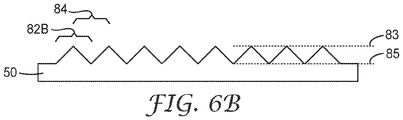
いくつかの実施例では、研磨パッド40は、研磨パッド40のセルの作業表面に延びて微細構造を形成する空洞によって形成された複数の微細構造を含んでもよい。図6Bは、本明細書で論じるいくつかの実施形態による、突起82B及び空洞84を含む微細構造を有する、セル50の作業表面の一部の概略断面図である。空洞は、任意の所望の距離だけ研磨パッド40内に延びてもよい(研磨パッド40を完全に通過することにより、空洞を通るスラリー流を可能にすることを含む)。空洞84は、任意のサイズ及び形状を有してもよい。例えば、キャビティ84の形状は、立方体、円筒形、プリズム形、半球形、直方体、角錐形、切頭角錐形、円錐形、切頭円錐形、十字形、弓状若しくは平坦な底部表面を持つ柱状、又はこれらの組み合わせ等の多数の幾何学的形状の中から選択され得る。あるいは、空洞84のいくつか又は全てが不規則形状を有してもよい。いくつかの実施形態では、空洞84のそれぞれは、同じ形状を有する。あるいは、任意の数の空洞84が、他の任意の数の空洞とは異なる形状を有してもよい。空洞84は、空洞が行及び列に並べられる構成で提供する、パターン(例えば、渦巻状、螺旋状、コークスクリュー状、又は格子状)に分布する、又は「ランダム」に(すなわち、規則的なパターンではない)分布することができる。微細構造の空洞の例としては、参照により本明細書に組み込まれる、米国出願公開第2016/0221146A1号を参照されたい。
In some embodiments, polishing
いくつかの実施形態では、研磨パッド40は、固定研磨パッドであってもよく、複数の微細構造は、研磨粒子を含む研磨材複合体であってもよい。図6Cは、本明細書で論じるいくつかの実施形態による、研磨粒子86を含む研磨材複合体の突起82Cを含む微細構造を有する、セル50の作業表面の一部の概略断面図である。固定研磨パッドは、二次元の、例えば、研磨粒子の層が1以上の樹脂若しくはバインダ層により裏材に保持された従来の研磨シートであってもよく、又は固定研磨パッドは、三次元固定研磨材、すなわち、分散した研磨粒子を含有する樹脂若しくはバインダ層であってもよく、樹脂/研磨複合体が使用中に摩耗すること及び/又はドレッシングが研磨粒子の未使用の層を露出させることを可能にするのに適切な高さを有する、樹脂/研磨複合体を形成する。砥粒物品は、第1の表面及び作業面を有する、三次元、テクスチャード、軟質の固定砥粒構造を含んでいてもよい。作業面は、複数の精密な形状の砥粒複合体を含んでいてもよい。精密な形状の砥粒複合体は、樹脂相及び砥粒相を含んでいてもよい。研磨複合微細構造の例としては、参照により本明細書に組み込まれる米国特許第7,160,178 B2号を参照されたい。精密な形状の砥粒複合体は、三次元、テクスチャード、軟質の固定砥粒構造を形成する配列に配置されていてもよい。砥粒物品は、パターン化された砥粒構造を含んでいてもよい。TRIZACT砥粒の商品名で入手可能な砥粒物品及び3M Company(ミネソタ州、セントポール)から入手可能なTRIZACTダイヤモンドタイル砥粒が、例示的なパターン化砥粒である。パターン化砥粒物品は、ダイ、成形型又は他の手法から精密に配列及び製造される、砥粒複合体のモノリシックな列を含む。こうしたパターン化砥粒物品は、砥粒加工、研磨、又は同時に砥粒加工及び研磨を実行できる。
In some embodiments, polishing
いくつかの実施形態では、研磨パッド40は、突起及び/又は細孔を含む微細構造を有してもよい。図6Dは、本明細書で論じるいくつかの実施形態による、突起82D及び細孔88を含む微細構造を有する、セル50の作業表面の一部の概略断面図である。細孔88の形状は、特に限定されず、円筒形、半球形、立方体、直方柱、三角柱、六角柱、三角錐、四、五、及び六角錐、角錐台、円錘形、円錐台等を含み得るが、それらに限定されない。細孔88の形状は、全て同じでよく、又は組み合わせが用いられてもよい。いくつかの実施形態において、細孔88の深さは、それぞれの正確に成形された細孔に隣接するランド領域の厚さ未満である、すなわち正確に成形された細孔は、ランド領域の厚さ全体を貫通する貫通穴ではない。これによって、細孔は作業面の近傍の流体を捕らえ、かつ保有することができる。正確に成形された突起88は、均一に分配され得る、すなわち、研磨層の表面にわたって単一の面密度を有し得る、又は研磨層10の表面にわたって異なる面密度を有し得る。細孔88は、研磨層の表面にわたってランダムに配置されてもよい、又は研磨層にわたって、例えば繰り返しパターン等のパターンで配置されてもよい。パターンとして、正方配列、及び六方配列等が挙げられるが、これらに限定されない。パターンの組み合わせを用いてもよい。突起及び細孔の例としては、参照により本明細書に組み込まれる、国際出願公開第2015/153601A1号を参照されたい。
In some embodiments, polishing
いくつかの実施形態では、研磨溶液30が、研磨作業において研磨パッド40と共に使用されてもよい。いくつかの実施形態では、本開示の研磨溶液30(一般に「スラリー」と呼ばれる)は、分散した及び/又は懸濁した研磨材複合体を有する流体成分を含んでいてもよい。
In some embodiments, polishing
種々の実施形態では、流体成分は、非水性又は水性であってよい。非水性流体成分としては、アルコール、アセテート、ケトン、有機酸、エーテル、又はこれらの組み合わせが挙げられる。水性流体成分は、上記の非水性流体のいずれかを含む、非水性流体成分を(水に加えて)含んでよい。流体成分が水性流体と非水性流体の両方を含むとき、得られる流体成分は、均質である、すなわち単相溶液であってもよい。例示的な実施形態では、流体成分は、研磨材複合体粒子が流体成分に不溶性であるように選択することができる。 In various embodiments, fluid components may be non-aqueous or aqueous. Non-aqueous fluid components include alcohols, acetates, ketones, organic acids, ethers, or combinations thereof. The aqueous fluid component may contain (in addition to water) a non-aqueous fluid component, including any of the non-aqueous fluids described above. When the fluid composition contains both aqueous and non-aqueous fluids, the resulting fluid composition may be homogeneous, ie, a single-phase solution. In exemplary embodiments, the fluid component can be selected such that the abrasive composite particles are insoluble in the fluid component.
いくつかの実施形態では、流体成分は、例えば、分散助剤、レオロジー変性剤、腐食防止剤、pH調整剤、界面活性剤、キレート剤/錯化剤、不動態化剤、発泡防止剤、及びこれらの組み合わせ等の1種以上の添加剤を更に含んでよい。分散助剤は、多くの場合、整合性のない又は好ましくない研磨性能をもたらす場合がある、スラリー中の凝集粒子の沈下、沈降、沈殿及び/又は軟凝集を防ぐために添加される。有用な分散剤としては、比較的高分子量の脂肪族又は脂環式ハロゲン化物及びアミンの反応生成物であるアミン分散剤が挙げられる。レオロジー変性剤としては、剪断減粘剤及び剪断増粘剤が挙げられる。剪断減粘剤としては、ポリオレフィンポリマー材料上にコーティングされたポリアミドワックスが挙げられる。剪断増粘剤としては、ヒュームドシリカ、水溶性ポリマー、及び非水性ポリマーが挙げられる。流体成分に添加することができる腐食防止剤には、金属を劣化させ得る研磨プロセスの酸性副生成物を中和できる、トリエタノールアミン、脂肪族アミン、オクタン酸オクチルアミン等のアルカリ性物質、並びにドデセニルコハク酸又は無水物及びオレイン酸等の脂肪酸とポリアミンとの縮合生成物が挙げられる。使用することができる好適なpH調整剤には、アルカリ金属水酸化物、アルカリ土類金属水酸化物、塩基性塩、有機アミン、アンモニア及びアンモニウム塩が挙げられる。また、緩衝系を用いてもよい。緩衝剤は、酸性から中性近くそして塩基性までの範囲にまたがるように調節することができる。使用することができる界面活性剤には、イオン性及び非イオン性界面活性剤が挙げられる。非イオン性界面活性剤としては、親水性及び疎水性セグメントを含有するポリマーが挙げられる。イオン性界面活性剤には、カチオン性界面活性剤とアニオン性界面活性剤の両方を挙げることができる。アニオン性界面活性剤は、水中で、両親媒性アニオンと、通常はアルカリ金属(Na+、K+)又は第四級アンモニウムであるカチオンとに解離する。界面活性剤は、単独で又は2種以上の組み合わせで使用することができる。 In some embodiments, fluid components include, for example, dispersing aids, rheology modifiers, corrosion inhibitors, pH modifiers, surfactants, chelating/complexing agents, passivating agents, antifoaming agents, and It may further comprise one or more additives such as combinations of these. Dispersing aids are often added to prevent settling, settling, precipitation and/or flocculation of agglomerated particles in the slurry, which can result in inconsistent or undesirable polishing performance. Useful dispersants include amine dispersants which are reaction products of relatively high molecular weight aliphatic or cycloaliphatic halides and amines. Rheology modifiers include shear thinning agents and shear thickening agents. Shear thinning agents include polyamide waxes coated onto polyolefin polymer materials. Shear thickeners include fumed silica, water-soluble polymers, and non-aqueous polymers. Corrosion inhibitors that can be added to the fluid components include alkaline substances such as triethanolamine, aliphatic amines, octylamine octoate, and dodecenyl succinate, which can neutralize acidic byproducts of the polishing process that can degrade metals. Condensation products of acids or anhydrides and fatty acids such as oleic acid with polyamines are included. Suitable pH adjusters that can be used include alkali metal hydroxides, alkaline earth metal hydroxides, basic salts, organic amines, ammonia and ammonium salts. A buffer system may also be used. Buffers can be adjusted to span the range from acidic to near neutral to basic. Surfactants that can be used include ionic and nonionic surfactants. Nonionic surfactants include polymers containing hydrophilic and hydrophobic segments. Ionic surfactants can include both cationic and anionic surfactants. Anionic surfactants dissociate in water into amphiphilic anions and cations, usually alkali metals (Na+, K+) or quaternary ammoniums. Surfactants can be used alone or in combination of two or more.
配位子及びキレート剤等の錯化剤は、特に、用途が金属仕上げ又は研磨に関する場合であって、使用中に金属の削り屑及び/又は金属イオンが流体成分中に存在し得るとき、流体成分に含めることができる。金属の酸化及び溶解は、錯化剤の添加によって促進することができる。これらの化合物は、金属に結合して、水性及び非水性液体中の金属又は金属酸化物の溶解度を高めることができる。錯化剤としては、1つのカルボキシル基(すなわち、単官能性カルボン酸)又は複数のカルボン酸基(すなわち、多官能性カルボン酸)を有するカルボン酸及びその塩が挙げられる。不動態化剤は、研磨する基材20上に不動態化層を作製するために、流体成分に添加することができ、これにより、基材20の除去速度を変更したり、又は基材20が2つ以上の異なる材料を含む表面を備える場合に、1つの材料の除去速度を別の材料に対して調整したりすることができる。使用され得る発泡阻害剤としては、シリコーン、エチルアクリレートと2-エチルヘキシルアクリレートとのコポリマー、及び乳化破壊剤が挙げられる。流体成分中で有用であり得る他の添加剤には、酸化剤及び/又は漂白剤、例えば過酸化水素、硝酸、硝酸第二鉄等の遷移金属錯体、潤滑剤、殺生物剤、石鹸等が挙げられる。様々な実施形態において、研磨溶液中の添加剤クラスの濃度、すなわち、1つの添加剤クラスからの1つ以上の添加剤の濃度は、研磨溶液の重量に基づいて少なくとも約0.01重量%かつ約20重量%未満であってもよい。
Complexing agents such as ligands and chelating agents are particularly useful when the application relates to metal finishing or polishing and metal shavings and/or metal ions may be present in the fluid components during use. can be included in the ingredients. Oxidation and dissolution of metals can be accelerated by the addition of complexing agents. These compounds can bind to metals and increase the solubility of metals or metal oxides in aqueous and non-aqueous liquids. Complexing agents include carboxylic acids and salts thereof having one carboxylic group (ie, monofunctional carboxylic acid) or multiple carboxylic acid groups (ie, multifunctional carboxylic acid). Passivating agents can be added to the fluid composition to create a passivating layer on the
研磨材複合体は、多細孔質セラミック研磨材複合体を含んでもよい。多孔質セラミック研磨材複合体は、多孔質セラミックマトリックス中に分散された個々の研磨粒子を含んでよい。本明細書で使用する場合、「セラミックマトリックス」という用語は、ガラス質と結晶質の両方のセラミック材料を含む。例示的な実施形態では、セラミックマトリックスの少なくとも一部は、ガラス質セラミック材料を含む。種々の実施形態では、セラミックマトリックスは、金属酸化物、例えば、酸化アルミニウム、酸化ホウ素、酸化ケイ素、酸化マグネシウム、酸化ナトリウム、酸化マンガン、酸化亜鉛及びこれらの混合物を含むガラスを含んでよい。本明細書で使用する場合、「多孔質」という用語は、その集合体全体にわたって分布する細孔又は間隙を有することを特徴とするセラミックマトリックスの構造を記述するために用いられる。細孔は、複合体の外表面に向かって開かれていてもよいし、塞がれていてもよい。セラミックマトリックス中の細孔は、セラミック研磨材複合体の破損の制御を助け、使用済み(すなわち劣化した)研磨粒子が複合体から放出されるようにすると考えられる。細孔はまた、研磨材物品と加工物との界面から削り屑及び使用済み研磨粒子を除去するための経路をもたらすことにより、研磨材物品の性能(例えば、切削速度及び表面仕上げ)を向上させ得る。空隙は、複合体の少なくとも約4体積%かつ複合体の95体積%未満を含んでもよい。いくつかの実施形態では、研磨粒子には、ダイヤモンド、立方晶窒化ホウ素、溶融酸化アルミニウム、セラミック酸化アルミニウム、熱処理した酸化アルミニウム、炭化ケイ素、炭化ホウ素、アルミナジルコニア、酸化鉄、セリア、ガーネット及びこれらの組み合わせを挙げることができる。種々の実施形態では、本開示の研磨材複合体粒子は、充填剤、カップリング剤、界面活性剤及び発泡抑制剤等の任意選択の添加剤も含んでよい。これらの材料の量は、所望の特性をもたらすように選択され得る。 The abrasive composites may comprise porous ceramic abrasive composites. Porous ceramic abrasive composites may comprise individual abrasive particles dispersed in a porous ceramic matrix. As used herein, the term "ceramic matrix" includes both vitreous and crystalline ceramic materials. In exemplary embodiments, at least a portion of the ceramic matrix comprises a vitreous ceramic material. In various embodiments, the ceramic matrix may comprise metal oxides, such as glass, including aluminum oxide, boron oxide, silicon oxide, magnesium oxide, sodium oxide, manganese oxide, zinc oxide, and mixtures thereof. As used herein, the term "porous" is used to describe the structure of a ceramic matrix characterized by having pores or interstices distributed throughout its mass. The pores may be open toward the outer surface of the composite or closed. It is believed that the pores in the ceramic matrix help control failure of the ceramic abrasive composites and allow spent (ie, degraded) abrasive particles to be released from the composites. Pores also improve abrasive article performance (e.g., cut rate and surface finish) by providing pathways for removal of swarf and spent abrasive particles from the abrasive article-workpiece interface. obtain. The voids may comprise at least about 4% by volume of the composite and less than 95% by volume of the composite. In some embodiments, the abrasive particles include diamond, cubic boron nitride, fused aluminum oxide, ceramic aluminum oxide, heat treated aluminum oxide, silicon carbide, boron carbide, alumina zirconia, iron oxide, ceria, garnet, and the like. Combinations can be mentioned. In various embodiments, the abrasive composite particles of the present disclosure may also include optional additives such as fillers, coupling agents, surfactants and foam control agents. The amounts of these materials can be selected to provide desired properties.
研磨複合体は、研磨複合体の1つ以上(最大で全て)が空洞内に少なくとも部分的に配置され得るように、研磨パッド40の微細構造のサイズ及び形状に対してサイズと形状が決定されてもよい。より具体的には、研磨複合体は、研磨複合体の1つ以上(最大で全て)が、空洞又は微細構造間に完全に受容されたときに、少なくとも空洞の開口部又は微細構造の間隙を越えて延在する部分を有するように、空洞又は微細構造に対してサイズと形状が決定されてもよい。本明細書で使用するとき、「完全に受容された」という語句は、空洞又は微細構造の間隙内の複合体の位置に関連する際、複合体が非破壊的圧縮力(例えば、以下で論じるように、研磨動作中に存在する力)の印加時に空洞又は微細構造間隙内で達成され得る。このように、以下で更に詳細に説明するように、研磨作業中、研磨溶液30の研磨複合粒子は、空洞又は微細構造の間隙内に受容され(例えば、摩擦力を介して)保持されることによって、研磨作業表面として機能することができる。
The abrasive composites are sized and shaped with respect to the size and shape of the microstructures of the
種々の実施形態では、研磨材複合体粒子は、精密な形状であってもよいし、不規則な形状(すなわち精密でない形状)であってもよい。精密な形状のセラミック研磨材複合体は、任意の形状(例えば、立方体、ブロック状、円筒形、角柱形、角錐形、切頭角錐形、円錐形、切頭円錐形、球形、半球形、十字形又は柱様)であってよい。研磨材複合体粒子は、異なる形状及び/又はサイズの研磨材複合体の混合物であってもよい。あるいは、研磨材複合体粒子は、同じ(又は実質的に同じ)形状及び/又はサイズを有してもよい。精密でない形状の粒子には、回転楕円体が挙げられ、例えば、噴霧乾燥プロセスにより形成することができる。様々な実施形態において、流体成分中の研磨材複合体の濃度は、少なくとも0.065重量%かつ6.5重量%未満であってもよい。いくつかの実施形態では、セラミック研磨材複合体とその作製にて使用される剥離剤の両方を流体成分中に含めることができる。これらの実施形態では、流体成分中の研磨材複合体及び剥離剤の濃度は、少なくとも01重量%及び10重量%未満であってもよい。 In various embodiments, the abrasive composite particles may be precisely shaped or irregularly shaped (ie, imprecisely shaped). Precisely shaped ceramic abrasive composites may be of any shape (e.g., cubic, blocky, cylindrical, prismatic, pyramidal, truncated pyramidal, conical, truncated conical, spherical, hemispherical, hexagonal). glyph-like or column-like). The abrasive composite particles may be a mixture of different shapes and/or sizes of abrasive composites. Alternatively, the abrasive composite particles may have the same (or substantially the same) shape and/or size. Imprecisely shaped particles include spheroids and can be formed, for example, by a spray drying process. In various embodiments, the concentration of abrasive composites in the fluid component may be at least 0.065 wt% and less than 6.5 wt%. In some embodiments, both the ceramic abrasive composites and the release agent used in making them can be included in the fluid component. In these embodiments, the concentration of abrasive composites and release agent in the fluid component may be at least 01 wt % and less than 10 wt %.
いくつかの実施形態では、本開示の研磨材複合体粒子は、研磨材スラリーに有益な特性を付与する試薬で表面改質(例えば、共有結合、イオン結合又は機械的結合)を施してよい。例えば、ガラス表面を酸又は塩基でエッチングして、適切な表面pHをもたらすことができる。共有結合による改質表面は、1種以上の表面処理剤を含む表面処理で粒子を反応させることによって作製することができる。表面処理剤は、改質を施す表面の疎水的性質又は親水的性質を調整するために使用することができる。スパッタリング、真空蒸発、化学蒸着(CVD)、又は溶融金属技術を用いることができる。 In some embodiments, abrasive composite particles of the present disclosure may be surface modified (eg, covalently, ionic or mechanically) with reagents that impart beneficial properties to the abrasive slurry. For example, a glass surface can be etched with acid or base to provide the appropriate surface pH. Covalently modified surfaces can be made by reacting particles with a surface treatment that includes one or more surface treatment agents. Surface treatment agents can be used to adjust the hydrophobic or hydrophilic properties of the surface to be modified. Sputtering, vacuum evaporation, chemical vapor deposition (CVD), or molten metal techniques can be used.
本開示は更に、上述の研磨パッドを使用した基材の研磨の方法に関する。図7は、本明細書で論じるいくつかの実施形態による、基材を研磨するための例示的な方法のフローチャートである。本方法は、研磨システム、例えば図1に関して記載したものを使用して、又は任意の他の従来の研磨システム、例えば片面若しくは両面研磨及びラッピングを用いて実施することができる。 The present disclosure further relates to methods of polishing substrates using the polishing pads described above. FIG. 7 is a flow chart of an exemplary method for polishing a substrate, according to some embodiments discussed herein. The method can be performed using a polishing system such as that described with respect to FIG. 1, or using any other conventional polishing system such as single or double sided polishing and lapping.
いくつかの実施形態において、基材の研磨方法は、研磨される基材20などの基材を準備すること(90)を含んでもよい。本方法は、研磨パッド40及び研磨溶液30などの、研磨パッドを準備すること(92)と、研磨溶液を準備すること(94)と、を更に含んでもよい。いくつかの実施形態において、本方法は、研磨パッドと基材(96)とを相対運動させながら、基材の表面を研磨パッド及び研磨溶液と接触させることを更に含んでもよい。例えば、図1の研磨システムを参照すると、プラテン12がキャリヤアセンブリ16に対して移動(例えば、並進及び/又は回転)させられる際、キャリヤアセンブリ16は、研磨溶液30が存在する状態で、基材20を(プラテン12に結合され得る)研磨パッド40の研磨表面18に対して押圧することができる。また、キャリヤアセンブリ16が、プラテン12に対して移動(例えば、並進及び/又は回転)させられてもよい。圧力及び相対運動の結果として、研磨粒子(研磨パッド40及び/又は研磨溶液30内/上に含有され得る)は、基材20の表面から材料を除去することができる。
In some embodiments, a method of polishing a substrate may include providing (90) a substrate, such as
例示的実施形態において、本開示のシステム及び方法は、超硬基材、例えば、サファイアのA、R、又はC面の仕上げに特に適する。完成したサファイアの結晶、シート、又はウェハは、例えば、発光ダイオード産業及び携帯ハンドヘルドデバイス用カバー層に有用である。かかる用途において、本システム及び方法は、材料の永続的な除去を提供する。更に、本開示のシステム及び方法は、通常用いられる小さい粒子サイズで実現される表面仕上げと同等の表面仕上げをもたらしつつ、通常用いられる大きい研磨粒子サイズで実現される除去速度と同程度の除去速度を提供できることが見出された。更にまた、本開示のシステム及び方法は、固定式研磨パッドで必要とされるようなパッドの広範囲なドレッシングを行うことなく、持続的な除去速度をもたらすことができる。 In exemplary embodiments, the systems and methods of the present disclosure are particularly suitable for finishing the A, R, or C faces of cemented carbide substrates, such as sapphire. Finished sapphire crystals, sheets, or wafers are useful, for example, in the light emitting diode industry and cover layers for portable handheld devices. In such applications, the system and method provide permanent removal of material. Further, the systems and methods of the present disclosure provide removal rates similar to those achieved with the larger abrasive particle sizes typically used while providing a surface finish comparable to that achieved with the smaller particle sizes typically used. was found to be able to provide Furthermore, the systems and methods of the present disclosure can provide sustained removal rates without extensive pad dressing, such as is required with fixed polishing pads.
本開示の操作を、以下の詳細な実施例に関連して更に説明する。これらの実施例は、様々な具体的な好ましい実施形態及び技術を更に示すために提供される。しかしながら、本開示の範囲内に留まりつつ、多くの変更及び修正を加えることができるということが理解されるべきである。 The operation of the present disclosure is further described with reference to the following detailed examples. These examples are provided to further demonstrate various specific preferred embodiments and techniques. However, it should be understood that many variations and modifications may be made while remaining within the scope of the present disclosure.
研磨パッドの作製 Fabrication of polishing pads
研磨パッドを次のとおり作製した。ポリカーボネートのシートを、米国特許第6,285,001号に記載されるようにレーザ研磨して、原型工具を形成した。原型工具をニッケルでメッキし、ニッケルネガを形成した。いくつかのニッケルネガを形成し、一緒に溶接してエンボス加工ロールを形成した。エンボス加工ロールは、米国特許出願公開第2010/0188751号に記載されるように、熱可塑性ポリウレタン用のエンボス加工プロセスにおいて使用されて研磨層を形成した。以下、研磨層の変形について説明する。 A polishing pad was prepared as follows. A sheet of polycarbonate was laser abraded as described in US Pat. No. 6,285,001 to form a prototype tool. A prototype tool was plated with nickel to form a nickel negative. Several nickel negatives were formed and welded together to form an embossed roll. The embossing roll was used in an embossing process for thermoplastic polyurethane to form an abrasive layer, as described in US Patent Application Publication No. 2010/0188751. The deformation of the polishing layer will be described below.
オフセット体積 offset volume
いくつかの実施例では、研磨層は、上述のように、微細複製中のポリマー変位のためのオフセット体積を生成する凹縁部を有するセルを有してもよい。第1の実施例では、研磨層は、ベース層の縁部から15ミクロンの高さ凹み、500ミクロンオフセットされている。第2の実施例では、研磨層は、ベース層の縁部から30ミクロンの高さ凹み、750ミクロンオフセットされている。 In some examples, the polishing layer may have cells with concave edges that create an offset volume for polymer displacement during microreplication, as described above. In a first example, the polishing layer is recessed 15 microns high and offset 500 microns from the edge of the base layer. In a second example, the polishing layer is offset 750 microns by a 30 micron height recess from the edge of the base layer.
図9Aは、第1の実施例の研磨パッド内のセルの高さマップである。図9Bは、10ミクロンの摩耗後の、第1の実施例の研磨パッド内のセルの接触領域のシミュレートされたマップである。図9Bのドットは、研磨パッドがウェハと接触する領域を示す。図9Bに見られるように、作業層はウェハと不均一な接触を有し、ベース層は左縁部及び上縁部においてウエハースと有意に接触している。 FIG. 9A is a height map of cells in the polishing pad of the first example. FIG. 9B is a simulated map of the contact area of cells in the polishing pad of the first example after 10 microns of wear. The dots in FIG. 9B indicate the areas where the polishing pad contacts the wafer. As seen in FIG. 9B, the working layer has non-uniform contact with the wafer and the base layer has significant contact with the wafer at the left and top edges.
図10Aは、第2の実施例の研磨パッド内のセルの高さマップである。図10Bは、10ミクロンの摩耗後の、第2の実施例の研磨パッド内のセルの接触領域のシミュレートされたマップである。図10Bに見られるように、作業層はウェハと均一な接触を有し、ベース層は、第1の実施例よりも著しく低い接触を有する。 FIG. 10A is a height map of cells in the polishing pad of the second example. FIG. 10B is a simulated map of the contact area of cells in the second example polishing pad after 10 microns of wear. As can be seen in FIG. 10B, the working layer has uniform contact with the wafer and the base layer has significantly lower contact than in the first embodiment.
本発明の様々な実施形態を説明した。これらの実施形態及び他の実施形態は、以下の特許請求の範囲に含まれる。
なお、以上の各実施形態に加えて以下の態様について付記する。
(付記1)
複数のチャネルによって分離された複数の隆起したセルを含む研磨層を備え、
前記複数の隆起したセルのそれぞれは、
複数の微細構造を含む微細構造化作業表面であって、前記複数の微細構造の頂部が上面を画定し、前記複数の微細構造の基部がベース面を画定する、微細構造化作業表面と、
前記複数のチャネルの壁を画定する実質的に垂直なチャネル表面であって、チャネル面を画定するチャネル表面と、
前記作業表面の縁部と前記チャネル表面の上縁部との間のオフセット表面と、
を含む、物品。
(付記2)
前記オフセット表面は、変位した材料の非平面部分を含み、前記変位した材料の山部が、前記作業表面に平行な変位面を画定する、付記1に記載の物品。
(付記3)
前記変位面は、前記ベース面の下方にある、付記2に記載の物品。
(付記4)
前記上面からの前記変位面の深さが、前記複数の微細構造の平均高さよりも大きい、付記2に記載の物品。
(付記5)
前記上面からの前記変位面の深さは、少なくとも10μmである、付記2に記載の物品。
(付記6)
前記上面からの前記変位面の深さは、5μm未満である、付記2に記載の物品。
(付記7)
前記上面、前記チャネル面、及び前記オフセット表面は、オフセット体積を画定する、付記6に記載の物品。
(付記8)
前記作業表面の前記縁部は、隣接するチャネル面からオフセット幅又はオフセット長さだけオフセットされている、付記7に記載の物品。
(付記9)
前記オフセット幅又はオフセット長さは、約10μm~1mmである、付記8に記載の物品。
(付記10)
前記オフセット幅又はオフセット長さは、前記作業表面の幅又は長さの約1%~約50%である、付記8に記載の物品。
(付記11)
前記隆起したセルは、多角形である、付記1に記載の物品。
(付記12)
前記隆起したセルは、矩形、三角形、円形、又は楕円形である、付記1に記載の物品。
(付記13)
前記複数のチャネルの少なくとも一部は、前記物品の長さにわたって連続的である、付記1に記載の物品。
(付記14)
前記複数のチャネルの少なくとも一部は、前記物品の長さにわたって不連続である、付記1に記載の物品。
(付記15)
前記複数のセルは、ヘリンボーン、クロスハッチ、又は湾曲パターンである、付記14に記載の物品。
(付記16)
前記微細構造化作業表面は、複数の細孔及び複数の凹凸を含む、付記15に記載の物品。
(付記17)
前記オフセット表面の少なくとも一部は、実質的に垂直な段付き表面を有する、付記16に記載の物品。
(付記18)
前記オフセット表面は、階段状表面、角度付き表面、及び湾曲表面のうちの少なくとも1つである、付記17に記載の物品。
(付記19)
前記オフセット表面は、実質的に垂直な上部と傾斜した下部とを含む、付記18に記載の物品。
(付記20)
前記研磨層とは異なる熱膨張係数を有する第2の層を前記研磨層の下方に更に備える、付記1に記載の物品。
(付記21)
基材を保持するように構成されたキャリヤアセンブリと、
付記1に記載の物品を備える研磨パッドと、
前記研磨パッドに連結されたプラテンと、
流体成分と研磨成分とを含む研磨溶液と、
を備え、
前記研磨パッドを前記基材に対して移動させるように構成されているシステム。
(付記22)
主表面を有する基材を準備することと、
付記1に記載の前記物品を備える研磨パッドを準備することと、
流体成分及び研磨成分を含む研磨溶液を含むことと、
前記研磨パッドと前記基材の前記主表面とを相対運動させながら、前記基材の前記主表面を前記研磨パッド及び前記研磨溶液と接触させることと、
を含む、方法。
(付記23)
付記1に記載の前記物品の作業表面と、前記チャネル表面と、前記オフセット表面と、に対応する構造化表面を有する高精細ツール。
(付記24)
前記構造化表面は、高精細中の材料の変位に適応するオフセット表面を形成するように構成されている、付記23に記載の高精細ツール。
(付記25)
前記変位した材料が前記ベース面の下方にくるように、前記構造化表面は、前記オフセット表面に対応する部分を有して構成されている、付記23に記載の高精細ツール。
(付記26)
前記変位した材料が前記上面の公差内に収まるように、前記構造化表面は、前記オフセット表面に対応する部分を有して構成されている、付記23に記載の高精細ツール。
(付記27)
前記公差は、5μm未満である、付記26に記載の高精細ツール。
Various embodiments of the invention have been described. These and other embodiments are within the scope of the following claims.
In addition to the above embodiments, the following aspects will be added.
(Appendix 1)
a polishing layer comprising a plurality of raised cells separated by a plurality of channels;
each of the plurality of raised cells comprising:
a microstructured work surface comprising a plurality of microstructures, wherein tops of the plurality of microstructures define a top surface and bases of the plurality of microstructures define a base surface;
substantially vertical channel surfaces defining walls of the plurality of channels, the channel surfaces defining channel faces;
an offset surface between the edge of the work surface and the upper edge of the channel surface;
Goods, including
(Appendix 2)
2. The article of
(Appendix 3)
3. The article of
(Appendix 4)
3. The article of
(Appendix 5)
3. The article of
(Appendix 6)
3. The article of
(Appendix 7)
7. The article of clause 6, wherein the top surface, the channel surface, and the offset surface define an offset volume.
(Appendix 8)
8. The article of Claim 7, wherein the edge of the work surface is offset from an adjacent channel face by an offset width or an offset length.
(Appendix 9)
9. The article of paragraph 8, wherein the offset width or offset length is between about 10 μm and 1 mm.
(Appendix 10)
9. The article of Clause 8, wherein the offset width or offset length is from about 1% to about 50% of the work surface width or length.
(Appendix 11)
(Appendix 12)
10. The article of
(Appendix 13)
(Appendix 14)
(Appendix 15)
15. The article of
(Appendix 16)
16. The article of clause 15, wherein the microstructured work surface comprises a plurality of pores and a plurality of asperities.
(Appendix 17)
17. The article of
(Appendix 18)
18. The article of clause 17, wherein the offset surface is at least one of a stepped surface, an angled surface, and a curved surface.
(Appendix 19)
19. The article of
(Appendix 20)
(Appendix 21)
a carrier assembly configured to hold a substrate;
A polishing pad comprising the article according to
a platen connected to the polishing pad;
a polishing solution comprising a fluid component and a polishing component;
with
A system configured to move the polishing pad relative to the substrate.
(Appendix 22)
providing a substrate having a major surface;
Providing a polishing pad comprising the article of
comprising a polishing solution comprising a fluid component and a polishing component;
contacting the major surface of the substrate with the polishing pad and the polishing solution while causing relative motion between the polishing pad and the major surface of the substrate;
A method, including
(Appendix 23)
A high definition tool having a structured surface corresponding to the working surface of the article of
(Appendix 24)
24. The high definition tool of Clause 23, wherein the structured surface is configured to form an offset surface that accommodates material displacement during high definition.
(Appendix 25)
24. The high definition tool of Clause 23, wherein the structured surface is configured with portions corresponding to the offset surface such that the displaced material is below the base surface.
(Appendix 26)
24. The high definition tool of Clause 23, wherein the structured surface is configured with portions corresponding to the offset surface such that the displaced material is within tolerance of the top surface.
(Appendix 27)
27. The high definition tool of Clause 26, wherein the tolerance is less than 5 μm.
Claims (14)
前記複数の隆起したセルのそれぞれは、
複数の微細構造を含む微細構造化作業表面であって、前記複数の微細構造の頂部が上面を画定し、前記複数の微細構造の基部がベース面を画定する、微細構造化作業表面と、
前記複数のチャネルの壁を画定する実質的に垂直なチャネル表面であって、チャネル面を画定するチャネル表面と、
前記作業表面の縁部と前記チャネル表面の上縁部との間のオフセット表面と、
を含み、
前記オフセット表面は、変位した材料の非平面部分を含み、前記変位した材料の山部が、前記作業表面に平行な変位面を画定し、
前記変位面が、前記オフセット表面より上方、且つ、前記ベース面より下方にある、物品。 a polishing layer comprising a plurality of raised cells separated by a plurality of channels;
each of the plurality of raised cells comprising:
a microstructured work surface comprising a plurality of microstructures, wherein tops of the plurality of microstructures define a top surface and bases of the plurality of microstructures define a base surface;
substantially vertical channel surfaces defining walls of the plurality of channels, the channel surfaces defining channel faces;
an offset surface between the edge of the work surface and the upper edge of the channel surface;
including
wherein the offset surface comprises a non-planar portion of displaced material, wherein peaks of the displaced material define a plane of displacement parallel to the work surface;
The article , wherein the displacement surface is above the offset surface and below the base surface .
請求項1に記載の物品を備える研磨パッドと、
前記研磨パッドに連結されたプラテンと、
流体成分と研磨成分とを含む研磨溶液と、
を備え、
前記研磨パッドを前記基材に対して移動させるように構成されているシステム。 a carrier assembly configured to hold a substrate;
A polishing pad comprising the article of claim 1;
a platen connected to the polishing pad;
a polishing solution comprising a fluid component and a polishing component;
with
A system configured to move the polishing pad relative to the substrate.
請求項1に記載の前記物品を備える研磨パッドを準備することと、
流体成分及び研磨成分を含む研磨溶液を含むことと、
前記研磨パッドと前記基材の前記主表面とを相対運動させながら、前記基材の前記主表面を前記研磨パッド及び前記研磨溶液と接触させることと、
を含む、方法。 providing a substrate having a major surface;
Providing a polishing pad comprising the article of claim 1;
comprising a polishing solution comprising a fluid component and a polishing component;
contacting the major surface of the substrate with the polishing pad and the polishing solution while causing relative motion between the polishing pad and the major surface of the substrate;
A method, including
Applications Claiming Priority (3)
| Application Number | Priority Date | Filing Date | Title |
|---|---|---|---|
| US201762541362P | 2017-08-04 | 2017-08-04 | |
| US62/541,362 | 2017-08-04 | ||
| PCT/IB2018/055815 WO2019026021A1 (en) | 2017-08-04 | 2018-08-02 | Microreplicated polishing surface with enhanced co-planarity |
Publications (3)
| Publication Number | Publication Date |
|---|---|
| JP2020529332A JP2020529332A (en) | 2020-10-08 |
| JP2020529332A5 JP2020529332A5 (en) | 2021-09-09 |
| JP7165719B2 true JP7165719B2 (en) | 2022-11-04 |
Family
ID=65233633
Family Applications (1)
| Application Number | Title | Priority Date | Filing Date |
|---|---|---|---|
| JP2020505906A Active JP7165719B2 (en) | 2017-08-04 | 2018-08-02 | Microreplicated polished surface with improved flatness |
Country Status (6)
| Country | Link |
|---|---|
| US (1) | US20200164484A1 (en) |
| JP (1) | JP7165719B2 (en) |
| KR (1) | KR102608124B1 (en) |
| CN (1) | CN111032284B (en) |
| TW (1) | TWI803502B (en) |
| WO (1) | WO2019026021A1 (en) |
Families Citing this family (3)
| Publication number | Priority date | Publication date | Assignee | Title |
|---|---|---|---|---|
| WO2021090122A1 (en) * | 2019-11-04 | 2021-05-14 | 3M Innovative Properties Company | Polishing article, polishing system and method of polishing |
| US20220395962A1 (en) * | 2019-11-05 | 2022-12-15 | 3M Innovative Properties Company | Molded Abrasive Rotary Tool |
| JP7435436B2 (en) * | 2020-12-24 | 2024-02-21 | 株式会社Sumco | How to polish carrier plate |
Citations (4)
| Publication number | Priority date | Publication date | Assignee | Title |
|---|---|---|---|---|
| US20060178099A1 (en) | 2005-02-07 | 2006-08-10 | Inoac Corporation | Polishing pad |
| JP2013193181A (en) | 2012-03-21 | 2013-09-30 | Fujibo Holdings Inc | Sheet for polishing pad, method for manufacturing the same, polishing pad, method for manufacturing the same, and polishing method |
| WO2017062719A1 (en) | 2015-10-07 | 2017-04-13 | 3M Innovative Properties Company | Polishing pads and systems and methods of making and using the same |
| JP2017510470A (en) | 2014-04-03 | 2017-04-13 | スリーエム イノベイティブ プロパティズ カンパニー | Polishing pad and system, and method for making and using the same |
Family Cites Families (26)
| Publication number | Priority date | Publication date | Assignee | Title |
|---|---|---|---|---|
| US5489233A (en) * | 1994-04-08 | 1996-02-06 | Rodel, Inc. | Polishing pads and methods for their use |
| US5921855A (en) * | 1997-05-15 | 1999-07-13 | Applied Materials, Inc. | Polishing pad having a grooved pattern for use in a chemical mechanical polishing system |
| US6780095B1 (en) * | 1997-12-30 | 2004-08-24 | Micron Technology, Inc. | Method and apparatus for mechanical and chemical-mechanical planarization of microelectronic substrates |
| FR2786118B1 (en) * | 1998-11-19 | 2000-12-22 | Lam Plan Sa | LAPPING OR POLISHING DEVICE |
| JP2000158327A (en) * | 1998-12-02 | 2000-06-13 | Rohm Co Ltd | Polishing cloth for chemimechanical polishing and chemimechanical polisher using same |
| US6439986B1 (en) * | 1999-10-12 | 2002-08-27 | Hunatech Co., Ltd. | Conditioner for polishing pad and method for manufacturing the same |
| US6776699B2 (en) * | 2000-08-14 | 2004-08-17 | 3M Innovative Properties Company | Abrasive pad for CMP |
| US7048615B2 (en) * | 2004-08-05 | 2006-05-23 | United Microelectronics Corp. | Pad backer and CMP process using the same |
| US7169029B2 (en) * | 2004-12-16 | 2007-01-30 | 3M Innovative Properties Company | Resilient structured sanding article |
| US20070128991A1 (en) * | 2005-12-07 | 2007-06-07 | Yoon Il-Young | Fixed abrasive polishing pad, method of preparing the same, and chemical mechanical polishing apparatus including the same |
| US7226345B1 (en) * | 2005-12-09 | 2007-06-05 | The Regents Of The University Of California | CMP pad with designed surface features |
| US7410413B2 (en) * | 2006-04-27 | 2008-08-12 | 3M Innovative Properties Company | Structured abrasive article and method of making and using the same |
| US7828634B2 (en) * | 2007-08-16 | 2010-11-09 | Rohm And Haas Electronic Materials Cmp Holdings, Inc. | Interconnected-multi-element-lattice polishing pad |
| EP2205521A4 (en) * | 2007-09-06 | 2013-09-11 | 3M Innovative Properties Co | Tool for making microstructured articles |
| US8425278B2 (en) * | 2009-08-26 | 2013-04-23 | 3M Innovative Properties Company | Structured abrasive article and method of using the same |
| CN102686362A (en) * | 2009-12-30 | 2012-09-19 | 3M创新有限公司 | Polishing pads including phase-separated polymer blend and method of making and using the same |
| JP5516051B2 (en) * | 2010-05-13 | 2014-06-11 | 旭硝子株式会社 | Polishing apparatus using polishing pad and glass plate manufacturing method |
| KR101161015B1 (en) * | 2010-09-10 | 2012-07-02 | 신한다이아몬드공업 주식회사 | Cmp pad conditioner and its manufacturing method |
| CN103328158A (en) * | 2011-01-26 | 2013-09-25 | 3M创新有限公司 | Abrasive article with replicated microstructured backing and method of using same |
| WO2012122186A2 (en) * | 2011-03-07 | 2012-09-13 | Entegris, Inc. | Chemical mechanical planarization pad conditioner |
| JP6188286B2 (en) * | 2012-07-13 | 2017-08-30 | スリーエム イノベイティブ プロパティズ カンパニー | Polishing pad and glass, ceramics, and metal material polishing method |
| US9649742B2 (en) * | 2013-01-22 | 2017-05-16 | Nexplanar Corporation | Polishing pad having polishing surface with continuous protrusions |
| US10160092B2 (en) * | 2013-03-14 | 2018-12-25 | Cabot Microelectronics Corporation | Polishing pad having polishing surface with continuous protrusions having tapered sidewalls |
| SG11201602207QA (en) * | 2013-09-25 | 2016-04-28 | 3M Innovative Properties Co | Multi-layered polishing pads |
| CN204277743U (en) * | 2014-10-29 | 2015-04-22 | 安阳方圆研磨材料有限责任公司 | Hard polishing pad |
| CN107614200B (en) * | 2015-05-13 | 2020-05-08 | 3M创新有限公司 | Polishing pad and system and method for using the same |
-
2018
- 2018-08-02 CN CN201880050836.9A patent/CN111032284B/en active Active
- 2018-08-02 US US16/636,348 patent/US20200164484A1/en active Pending
- 2018-08-02 WO PCT/IB2018/055815 patent/WO2019026021A1/en active Application Filing
- 2018-08-02 JP JP2020505906A patent/JP7165719B2/en active Active
- 2018-08-02 KR KR1020207004255A patent/KR102608124B1/en active IP Right Grant
- 2018-08-03 TW TW107127051A patent/TWI803502B/en active
Patent Citations (4)
| Publication number | Priority date | Publication date | Assignee | Title |
|---|---|---|---|---|
| US20060178099A1 (en) | 2005-02-07 | 2006-08-10 | Inoac Corporation | Polishing pad |
| JP2013193181A (en) | 2012-03-21 | 2013-09-30 | Fujibo Holdings Inc | Sheet for polishing pad, method for manufacturing the same, polishing pad, method for manufacturing the same, and polishing method |
| JP2017510470A (en) | 2014-04-03 | 2017-04-13 | スリーエム イノベイティブ プロパティズ カンパニー | Polishing pad and system, and method for making and using the same |
| WO2017062719A1 (en) | 2015-10-07 | 2017-04-13 | 3M Innovative Properties Company | Polishing pads and systems and methods of making and using the same |
Also Published As
| Publication number | Publication date |
|---|---|
| JP2020529332A (en) | 2020-10-08 |
| KR20200037269A (en) | 2020-04-08 |
| KR102608124B1 (en) | 2023-11-29 |
| CN111032284A (en) | 2020-04-17 |
| CN111032284B (en) | 2022-11-04 |
| TWI803502B (en) | 2023-06-01 |
| WO2019026021A1 (en) | 2019-02-07 |
| US20200164484A1 (en) | 2020-05-28 |
| TW201910056A (en) | 2019-03-16 |
Similar Documents
| Publication | Publication Date | Title |
|---|---|---|
| US11697185B2 (en) | Abrasive articles with precisely shaped features and method of making thereof | |
| TWI769988B (en) | Polishing pads and systems and methods of making and using the same | |
| US7762872B2 (en) | Superhard cutters and associated methods | |
| US9956664B2 (en) | Abrasive element precursor with precisely shaped features and methods of making thereof | |
| US7658666B2 (en) | Superhard cutters and associated methods | |
| EP2845221B1 (en) | Cmp conditioner pads with superabrasive grit enhancement | |
| JP7165719B2 (en) | Microreplicated polished surface with improved flatness | |
| CN102049723B (en) | Method for polishing semiconductor wafer | |
| US20090123705A1 (en) | CMP Pad Dressers | |
| WO2001026862A1 (en) | Conditioner for polishing pad and method for manufacturing the same | |
| US20190091832A1 (en) | Composite conditioner and associated methods | |
| EP1954446A1 (en) | Abrasive article and method of modifying the surface of a workpiece | |
| JP2002504864A (en) | Mosaic polishing pad and related method | |
| WO2008063599A2 (en) | Superhard cutters and associated methods | |
| KR20100110989A (en) | Cmp pad conditioner and its manufacturing method | |
| TWI383860B (en) | Modular dresser | |
| US20200171619A1 (en) | Surface projection polishing pad | |
| TW201127554A (en) | Resin bonding pad conditioner with surface recessed pattern and manufacture method thereof | |
| JP2005131779A (en) | Composite material tool plate for polishing | |
| KR200188920Y1 (en) | Conditioner for polishing pad | |
| CN110871407A (en) | Polishing pad dresser and method for chemical mechanical planarization | |
| CN112135709A (en) | Conditioner for chemical mechanical planarization pad and related method |
Legal Events
| Date | Code | Title | Description |
|---|---|---|---|
| A521 | Request for written amendment filed |
Free format text: JAPANESE INTERMEDIATE CODE: A523 Effective date: 20210730 |
|
| A621 | Written request for application examination |
Free format text: JAPANESE INTERMEDIATE CODE: A621 Effective date: 20210730 |
|
| A977 | Report on retrieval |
Free format text: JAPANESE INTERMEDIATE CODE: A971007 Effective date: 20220620 |
|
| A131 | Notification of reasons for refusal |
Free format text: JAPANESE INTERMEDIATE CODE: A131 Effective date: 20220705 |
|
| RD03 | Notification of appointment of power of attorney |
Free format text: JAPANESE INTERMEDIATE CODE: A7423 Effective date: 20220712 |
|
| A521 | Request for written amendment filed |
Free format text: JAPANESE INTERMEDIATE CODE: A523 Effective date: 20220720 |
|
| TRDD | Decision of grant or rejection written | ||
| A01 | Written decision to grant a patent or to grant a registration (utility model) |
Free format text: JAPANESE INTERMEDIATE CODE: A01 Effective date: 20220927 |
|
| A61 | First payment of annual fees (during grant procedure) |
Free format text: JAPANESE INTERMEDIATE CODE: A61 Effective date: 20221024 |
|
| R150 | Certificate of patent or registration of utility model |
Ref document number: 7165719 Country of ref document: JP Free format text: JAPANESE INTERMEDIATE CODE: R150 |