JP7120423B2 - Receiving device and receiving method - Google Patents
Receiving device and receiving method Download PDFInfo
- Publication number
- JP7120423B2 JP7120423B2 JP2021152130A JP2021152130A JP7120423B2 JP 7120423 B2 JP7120423 B2 JP 7120423B2 JP 2021152130 A JP2021152130 A JP 2021152130A JP 2021152130 A JP2021152130 A JP 2021152130A JP 7120423 B2 JP7120423 B2 JP 7120423B2
- Authority
- JP
- Japan
- Prior art keywords
- signaling
- layer
- physical layer
- symbol
- frame
- Prior art date
- Legal status (The legal status is an assumption and is not a legal conclusion. Google has not performed a legal analysis and makes no representation as to the accuracy of the status listed.)
- Active
Links
- 238000000034 method Methods 0.000 title claims description 223
- 230000011664 signaling Effects 0.000 claims description 413
- 238000012545 processing Methods 0.000 claims description 150
- 230000005540 biological transmission Effects 0.000 description 114
- 238000010586 diagram Methods 0.000 description 97
- 238000005516 engineering process Methods 0.000 description 79
- 238000004088 simulation Methods 0.000 description 21
- 238000004891 communication Methods 0.000 description 19
- 238000005070 sampling Methods 0.000 description 5
- 238000006243 chemical reaction Methods 0.000 description 3
- 238000001514 detection method Methods 0.000 description 2
- 230000000694 effects Effects 0.000 description 2
- 238000012986 modification Methods 0.000 description 2
- 230000004048 modification Effects 0.000 description 2
- 238000004904 shortening Methods 0.000 description 2
- 230000003139 buffering effect Effects 0.000 description 1
- 238000012937 correction Methods 0.000 description 1
- 230000006870 function Effects 0.000 description 1
- 230000010354 integration Effects 0.000 description 1
- 239000000203 mixture Substances 0.000 description 1
- 230000003287 optical effect Effects 0.000 description 1
- 230000010363 phase shift Effects 0.000 description 1
- 230000000717 retained effect Effects 0.000 description 1
- 239000004065 semiconductor Substances 0.000 description 1
Images


Classifications
-
- H—ELECTRICITY
- H04—ELECTRIC COMMUNICATION TECHNIQUE
- H04H—BROADCAST COMMUNICATION
- H04H20/00—Arrangements for broadcast or for distribution combined with broadcast
- H04H20/28—Arrangements for simultaneous broadcast of plural pieces of information
-
- H—ELECTRICITY
- H04—ELECTRIC COMMUNICATION TECHNIQUE
- H04H—BROADCAST COMMUNICATION
- H04H60/00—Arrangements for broadcast applications with a direct linking to broadcast information or broadcast space-time; Broadcast-related systems
- H04H60/68—Systems specially adapted for using specific information, e.g. geographical or meteorological information
- H04H60/73—Systems specially adapted for using specific information, e.g. geographical or meteorological information using meta-information
-
- H—ELECTRICITY
- H04—ELECTRIC COMMUNICATION TECHNIQUE
- H04J—MULTIPLEX COMMUNICATION
- H04J1/00—Frequency-division multiplex systems
- H04J1/02—Details
- H04J1/06—Arrangements for supplying the carrier waves ; Arrangements for supplying synchronisation signals
-
- H—ELECTRICITY
- H04—ELECTRIC COMMUNICATION TECHNIQUE
- H04J—MULTIPLEX COMMUNICATION
- H04J3/00—Time-division multiplex systems
-
- H—ELECTRICITY
- H04—ELECTRIC COMMUNICATION TECHNIQUE
- H04J—MULTIPLEX COMMUNICATION
- H04J3/00—Time-division multiplex systems
- H04J3/02—Details
- H04J3/06—Synchronising arrangements
- H04J3/0602—Systems characterised by the synchronising information used
- H04J3/0605—Special codes used as synchronising signal
-
- H—ELECTRICITY
- H04—ELECTRIC COMMUNICATION TECHNIQUE
- H04L—TRANSMISSION OF DIGITAL INFORMATION, e.g. TELEGRAPHIC COMMUNICATION
- H04L1/00—Arrangements for detecting or preventing errors in the information received
- H04L1/0001—Systems modifying transmission characteristics according to link quality, e.g. power backoff
- H04L1/0023—Systems modifying transmission characteristics according to link quality, e.g. power backoff characterised by the signalling
-
- H—ELECTRICITY
- H04—ELECTRIC COMMUNICATION TECHNIQUE
- H04L—TRANSMISSION OF DIGITAL INFORMATION, e.g. TELEGRAPHIC COMMUNICATION
- H04L1/00—Arrangements for detecting or preventing errors in the information received
- H04L1/004—Arrangements for detecting or preventing errors in the information received by using forward error control
- H04L1/0056—Systems characterized by the type of code used
- H04L1/0057—Block codes
-
- H—ELECTRICITY
- H04—ELECTRIC COMMUNICATION TECHNIQUE
- H04L—TRANSMISSION OF DIGITAL INFORMATION, e.g. TELEGRAPHIC COMMUNICATION
- H04L1/00—Arrangements for detecting or preventing errors in the information received
- H04L1/004—Arrangements for detecting or preventing errors in the information received by using forward error control
- H04L1/0056—Systems characterized by the type of code used
- H04L1/0061—Error detection codes
-
- H—ELECTRICITY
- H04—ELECTRIC COMMUNICATION TECHNIQUE
- H04L—TRANSMISSION OF DIGITAL INFORMATION, e.g. TELEGRAPHIC COMMUNICATION
- H04L1/00—Arrangements for detecting or preventing errors in the information received
- H04L1/004—Arrangements for detecting or preventing errors in the information received by using forward error control
- H04L1/0056—Systems characterized by the type of code used
- H04L1/0071—Use of interleaving
-
- H—ELECTRICITY
- H04—ELECTRIC COMMUNICATION TECHNIQUE
- H04N—PICTORIAL COMMUNICATION, e.g. TELEVISION
- H04N21/00—Selective content distribution, e.g. interactive television or video on demand [VOD]
- H04N21/20—Servers specifically adapted for the distribution of content, e.g. VOD servers; Operations thereof
- H04N21/23—Processing of content or additional data; Elementary server operations; Server middleware
- H04N21/236—Assembling of a multiplex stream, e.g. transport stream, by combining a video stream with other content or additional data, e.g. inserting a URL [Uniform Resource Locator] into a video stream, multiplexing software data into a video stream; Remultiplexing of multiplex streams; Insertion of stuffing bits into the multiplex stream, e.g. to obtain a constant bit-rate; Assembling of a packetised elementary stream
Landscapes
- Engineering & Computer Science (AREA)
- Signal Processing (AREA)
- Computer Networks & Wireless Communication (AREA)
- Multimedia (AREA)
- Quality & Reliability (AREA)
- Two-Way Televisions, Distribution Of Moving Picture Or The Like (AREA)
- Time-Division Multiplex Systems (AREA)
- Mobile Radio Communication Systems (AREA)
Description
本技術は、受信装置、及び、受信方法に関し、特に、複数の多重化の方式を、同一の放送システムで実現する場合に、より柔軟な運用を行うことができるようにした受信装置、及び、受信方法に関する。 The present technology relates to a receiving device and a receiving method, and in particular, a receiving device that enables more flexible operation when multiple multiplexing schemes are implemented in the same broadcasting system, and Receiving method.
例えば、地上デジタルテレビ放送の放送方式として、日本等が採用するISDB-T(Integrated Services Digital Broadcasting - Terrestrial)においては、放送信号の多重化の方式として、周波数分割多重化方式(FDM:Frequency Division Multiplexing)が採用されている(例えば、非特許文献1参照)。 For example, in ISDB-T (Integrated Services Digital Broadcasting - Terrestrial) adopted by Japan and other countries as a broadcasting system for digital terrestrial television broadcasting, frequency division multiplexing (FDM) is used as a broadcasting signal multiplexing system. ) is employed (see, for example, Non-Patent Document 1).
ところで、地上デジタルテレビ放送の次世代に向けた高度化の検討が行われている。次世代の地上デジタルテレビ放送においては、周波数分割多重化方式(FDM)のほか、時分割多重化方式(TDM:Time Division Multiplexing)や階層分割多重化方式(LDM:Layered Division Multiplexing)などの多重化の方式を用いた複数の放送システムが検討されている。 By the way, studies are underway to improve the next generation of terrestrial digital television broadcasting. In next-generation digital terrestrial television broadcasting, in addition to frequency division multiplexing (FDM), multiplexing such as time division multiplexing (TDM) and layered division multiplexing (LDM) A number of broadcasting systems using the method are being considered.
しかしながら、現状では、複数の多重化の方式を、同一の放送システムにより実現するための技術方式は確立されておらず、複数の多重化の方式を、同一の放送システムで実現する場合に、より柔軟な運用を行うための提案が要請されていた。 However, at present, there is no established technical method for implementing multiple multiplexing methods in the same broadcasting system. Proposals for flexible operation were requested.
本技術はこのような状況に鑑みてなされたものであり、複数の多重化の方式を、同一の放送システムで実現する場合に、より柔軟な運用を行うことができるようにするものである。 The present technology has been developed in view of such circumstances, and enables more flexible operation when multiple multiplexing methods are implemented in the same broadcasting system.
本技術の第1の側面の送信装置は、所定の多重化の方式で多重化された物理層フレームであって、多重化の方式を判別可能な判別情報を含む前記物理層フレームを生成する生成部と、前記物理層フレームを、放送信号として送信する送信部とを備える送信装置である。 A transmission device according to a first aspect of the present technology is a physical layer frame multiplexed by a predetermined multiplexing method, and generates the physical layer frame including determination information that can determine the multiplexing method. and a transmitter configured to transmit the physical layer frame as a broadcast signal.
本技術の第1の側面の送信装置は、独立した装置であってもよいし、1つの装置を構成している内部ブロックであってもよい。また、本技術の第1の側面の送信方法は、上述した本技術の第1の側面の送信装置に対応する送信方法である。 The transmitting device of the first aspect of the present technology may be an independent device, or may be an internal block forming one device. Moreover, the transmission method of the first aspect of the present technology is a transmission method corresponding to the transmission device of the first aspect of the present technology described above.
本技術の第1の側面の送信装置、及び、送信方法においては、所定の多重化の方式で多重化された物理層フレームであって、多重化の方式を判別可能な判別情報を含む前記物理層フレームが生成され、前記物理層フレームが、放送信号として送信される。 In the transmission device and the transmission method of the first aspect of the present technology, the physical layer frame multiplexed by a predetermined multiplexing scheme, the physical layer frame including discrimination information capable of discriminating the multiplexing scheme A layer frame is generated and the physical layer frame is transmitted as a broadcast signal.
本技術の第1の側面の受信装置は、放送信号を受信する受信部と、前記放送信号から得られる物理層フレームに含まれる判別情報に基づいて、所定の多重化の方式で多重化された前記物理層フレームの多重化の方式を判別し、前記物理層フレームを処理する処理部とを備える受信装置である。 A receiving device according to a first aspect of the present technology includes a receiving unit that receives a broadcast signal, and based on determination information included in a physical layer frame obtained from the broadcast signal, multiplexed by a predetermined multiplexing method and a processing unit that determines a multiplexing scheme of the physical layer frame and processes the physical layer frame.
本技術の第1の側面の受信装置は、独立した装置であってもよいし、1つの装置を構成している内部ブロックであってもよい。また、本技術の第1の側面の受信方法は、上述した本技術の第1の側面の受信装置に対応する受信方法である。 The receiving device of the first aspect of the present technology may be an independent device, or may be an internal block forming one device. Further, the receiving method of the first aspect of the present technology is a receiving method corresponding to the above-described receiving device of the first aspect of the present technology.
本技術の第1の側面の受信装置、及び、受信方法においては、放送信号が受信され、前記放送信号から得られる物理層フレームに含まれる判別情報に基づいて、所定の多重化の方式で多重化された前記物理層フレームの多重化の方式が判別され、前記物理層フレームが処理される。 In the receiving device and receiving method of the first aspect of the present technology, a broadcast signal is received and multiplexed by a predetermined multiplexing method based on discrimination information included in a physical layer frame obtained from the broadcast signal. A multiplexing scheme for the combined physical layer frame is determined, and the physical layer frame is processed.
本技術の第2の側面の送信装置は、所定の多重化の方式で多重化された物理層フレームであって、その先頭に、物理層のシグナリングが集中して配置された前記物理層フレームを生成する生成部と、前記物理層フレームを、放送信号として送信する送信部とを備える送信装置である。 A transmission device according to a second aspect of the present technology is a physical layer frame multiplexed by a predetermined multiplexing method, and the physical layer frame in which physical layer signaling is concentrated and arranged at the beginning thereof. The transmission device includes a generation unit that generates the physical layer frame and a transmission unit that transmits the physical layer frame as a broadcast signal.
本技術の第2の側面の送信装置は、独立した装置であってもよいし、1つの装置を構成している内部ブロックであってもよい。また、本技術の第2の側面の送信方法は、上述した本技術の第2の側面の送信装置に対応する送信方法である。 The transmitting device of the second aspect of the present technology may be an independent device, or may be an internal block forming one device. Further, a transmission method according to the second aspect of the present technology is a transmission method corresponding to the above-described transmission device according to the second aspect of the present technology.
本技術の第2の側面の送信装置、及び、送信方法においては、所定の多重化の方式で多重化された物理層フレームであって、その先頭に、物理層のシグナリングが集中して配置された前記物理層フレームが生成され、前記物理層フレームが、放送信号として送信される。 In the transmission device and transmission method of the second aspect of the present technology, a physical layer frame multiplexed by a predetermined multiplexing scheme, in which physical layer signaling is concentrated and arranged at the beginning thereof The physical layer frame is generated, and the physical layer frame is transmitted as a broadcast signal.
本技術の第2の側面の受信装置は、放送信号を受信する受信部と、前記放送信号から得られる物理層フレームの先頭に集中して配置された物理層のシグナリングを取得し、前記物理層フレームを処理する処理部とを備える受信装置である。 A receiving device according to a second aspect of the present technology includes a receiving unit that receives a broadcast signal, acquires physical layer signaling that is centrally arranged at the beginning of a physical layer frame obtained from the broadcast signal, and obtains the physical layer signaling. and a processing unit that processes frames.
本技術の第2の側面の受信装置は、独立した装置であってもよいし、1つの装置を構成している内部ブロックであってもよい。また、本技術の第2の側面の受信方法は、上述した本技術の第2の側面の受信装置に対応する受信方法である。 The receiving device of the second aspect of the present technology may be an independent device, or may be an internal block forming one device. Further, a receiving method according to the second aspect of the present technology is a receiving method corresponding to the above-described receiving device according to the second aspect of the present technology.
本技術の第2の側面の受信装置、及び、受信方法においては、放送信号が受信され、前記放送信号から得られる物理層フレームの先頭に集中して配置された物理層のシグナリングが取得され、前記物理層フレームが処理される。 In the receiving device and receiving method of the second aspect of the present technology, a broadcast signal is received, physical layer signaling concentratedly arranged at the beginning of a physical layer frame obtained from the broadcast signal is acquired, The physical layer frames are processed.
本技術の第3の側面の送信装置は、所定の多重化の方式で多重化された物理層フレームであって、階層ごとに、P2シンボルのP2シグナリングが配置された前記物理層フレームを生成する生成部と、前記物理層フレームを、放送信号として送信する送信部とを備える送信装置である。 A transmission device according to a third aspect of the present technology is a physical layer frame multiplexed by a predetermined multiplexing scheme, and generates the physical layer frame in which P2 signaling of P2 symbols is arranged for each layer. The transmission device includes a generation unit and a transmission unit that transmits the physical layer frame as a broadcast signal.
本技術の第3の側面の送信装置は、独立した装置であってもよいし、1つの装置を構成している内部ブロックであってもよい。また、本技術の第3の側面の送信方法は、上述した本技術の第3の側面の送信装置に対応する送信方法である。 The transmitting device according to the third aspect of the present technology may be an independent device, or may be an internal block forming one device. A transmission method according to the third aspect of the present technology is a transmission method corresponding to the above-described transmission device according to the third aspect of the present technology.
本技術の第3の側面の送信装置、及び、送信方法においては、所定の多重化の方式で多重化された物理層フレームであって、階層ごとに、P2シンボルのP2シグナリングが配置された前記物理層フレームが生成され、前記物理層フレームが、放送信号として送信される。 In the transmission device and transmission method of the third aspect of the present technology, the physical layer frame multiplexed by a predetermined multiplexing scheme, wherein P2 signaling of P2 symbols is arranged for each layer A physical layer frame is generated and the physical layer frame is transmitted as a broadcast signal.
本技術の第3の側面の受信装置は、放送信号を受信する受信部と、前記放送信号から得られる物理層フレームの階層ごとに配置されたP2シンボルのP2シグナリングを取得し、前記物理層フレームを処理する処理部とを備える受信装置である。 A receiving device according to a third aspect of the present technology includes a receiving unit that receives a broadcast signal, acquires P2 signaling of P2 symbols arranged for each layer of a physical layer frame obtained from the broadcast signal, and acquires the P2 signaling of the physical layer frame. and a processing unit for processing.
本技術の第3の側面の受信装置は、独立した装置であってもよいし、1つの装置を構成している内部ブロックであってもよい。また、本技術の第3の側面の受信方法は、上述した本技術の第3の側面の受信装置に対応する受信方法である。 The receiving device of the third aspect of the present technology may be an independent device, or may be an internal block forming one device. A receiving method according to the third aspect of the present technology is a receiving method corresponding to the above-described receiving device according to the third aspect of the present technology.
本技術の第3の側面の受信装置、及び、受信方法においては、放送信号が受信され、前記放送信号から得られる物理層フレームの階層ごとに配置されたP2シンボルのP2シグナリングが取得され、前記物理層フレームが処理される。 In the receiving device and receiving method of the third aspect of the present technology, a broadcast signal is received, P2 signaling of P2 symbols arranged for each layer of a physical layer frame obtained from the broadcast signal is acquired, and A physical layer frame is processed.
本技術の第1の側面乃至第3の側面によれば、複数の多重化の方式を、同一の放送システムで実現する場合に、より柔軟な運用を行うことができる。 According to the first to third aspects of the present technology, more flexible operation can be performed when multiple multiplexing schemes are implemented in the same broadcasting system.
なお、ここに記載された効果は必ずしも限定されるものではなく、本開示中に記載されたいずれかの効果であってもよい。 Note that the effects described here are not necessarily limited, and may be any of the effects described in the present disclosure.
以下、図面を参照しながら本技術の実施の形態について説明する。なお、説明は以下の順序で行うものとする。 Hereinafter, embodiments of the present technology will be described with reference to the drawings. Note that the description will be given in the following order.
1.システムの構成
2.本技術の概要
3.フレーム構成
4.第1の解決手法:多重化の方式(FDM,TDM,LDM)を判別する手法
(1)同期パターン解決手法
(2)P1シグナリング解決手法
5.P2シグナリングの構成
(1)L1Bシグナリングの構成
(2)L1Dシグナリングの構成
6.第2の解決手法:フレーム同期までの時間を短縮化する手法
7.第3の解決手法:プリアンブルをFDM化又はTDM化する手法
8.受信装置の動作
9.各解決手法に対応した処理の流れ
10.変形例
11.コンピュータの構成
1. System configuration2. Outline of this
<1.システムの構成> <1. System configuration>
(伝送システムの構成例)
図1は、本技術を適用した伝送システムの一実施の形態の構成を示すブロック図である。なお、システムとは、複数の装置が論理的に集合したものをいう。
(Configuration example of transmission system)
FIG. 1 is a block diagram showing the configuration of one embodiment of a transmission system to which the present technology is applied. A system is a logical assembly of a plurality of devices.
図1において、伝送システム1は、各放送局に関連する施設に設置されるデータ処理装置10-1乃至10-N(Nは1以上の整数)と、送信所に設置される送信装置20と、エンドユーザが所有する受信装置30-1乃至30-M(Mは1以上の整数)から構成される。
In FIG. 1, a
また、この伝送システム1において、データ処理装置10-1乃至10-Nと、送信装置20とは、通信回線40-1乃至40-Nを介して、接続されている。なお、通信回線40-1乃至40-Nは、例えば専用線とすることができる。
In this
データ処理装置10-1は、放送局Aにより制作された放送番組等のコンテンツを処理し、その結果得られる伝送データを、通信回線40-1を介して送信装置20に送信する。
The data processing device 10-1 processes contents such as broadcast programs produced by the broadcasting station A, and transmits transmission data obtained as a result to the
データ処理装置10-2乃至10-Nにおいては、データ処理装置10-1と同様に、放送局Bや放送局Z等の各放送局により制作された放送番組等のコンテンツが処理され、その結果得られる伝送データが、通信回線40-2乃至40-Nを介して、送信装置20に送信される。
In the data processing devices 10-2 to 10-N, similarly to the data processing device 10-1, contents such as broadcast programs produced by each broadcasting station such as broadcasting station B and broadcasting station Z are processed, and the result is The obtained transmission data is transmitted to the
送信装置20は、通信回線40-1乃至40-Nを介して、放送局側のデータ処理装置10-1乃至10-Nから送信されてくる伝送データを受信する。送信装置20は、データ処理装置10-1乃至10-Nからの伝送データを処理し、その結果得られる放送信号を、送信所に設置された送信用アンテナから送信する。
The transmitting
これにより、送信所側の送信装置20からの放送信号は、放送伝送路50を介して、受信装置30-1乃至30-Mに送信される。
As a result, broadcast signals from the transmitting
受信装置30-1乃至30-Mは、テレビ受像機やセットトップボックス(STB:Set Top Box)、録画機、ゲーム機、ネットワークストレージなどの固定受信機、あるいはスマートフォンや携帯電話機、タブレット型コンピュータ等のモバイル受信機である。また、受信装置30-1乃至30-Mは、例えば車載テレビなどの車両に搭載される車載機器や、ヘッドマウントディスプレイ(HMD:Head Mounted Display)等のウェアラブルコンピュータなどであってもよい。 Receiving devices 30-1 to 30-M are television receivers, set top boxes (STBs), recorders, game machines, stationary receivers such as network storage, smart phones, mobile phones, tablet computers, etc. mobile receiver. Further, the receiving devices 30-1 to 30-M may be, for example, in-vehicle equipment mounted in a vehicle such as an in-vehicle television, or a wearable computer such as a head mounted display (HMD).
受信装置30-1は、放送伝送路50を介して、送信装置20から送信されてくる放送信号を受信して処理することで、エンドユーザによる選局操作に応じた放送番組等のコンテンツを再生する。
The receiving device 30-1 receives and processes the broadcast signal transmitted from the transmitting
受信装置30-2乃至30-Mにおいては、受信装置30-1と同様に、送信装置20からの放送信号が処理され、エンドユーザによる選局操作に応じたコンテンツが再生される。
Similarly to the receiving device 30-1, the receiving devices 30-2 to 30-M process the broadcast signal from the transmitting
なお、伝送システム1において、放送伝送路50は、地上波(地上波放送)のほか、例えば、放送衛星(BS:Broadcasting Satellite)や通信衛星(CS:Communications Satellite)を利用した衛星放送、あるいは、ケーブルを用いた有線放送(CATV:Common Antenna TeleVision)などであってもよい。
In the
また、以下の説明では、放送局側のデータ処理装置10-1乃至10-Nを、特に区別する必要がない場合には、データ処理装置10と称する。また、受信装置30-1乃至30-Mを、特に区別する必要がない場合には、受信装置30と称する。
Further, in the following description, the data processing devices 10-1 to 10-N on the broadcasting station side will be referred to as
(送信側の装置の構成)
図2は、図1のデータ処理装置10と送信装置20の構成例を示すブロック図である。
(Configuration of device on the transmitting side)
FIG. 2 is a block diagram showing a configuration example of the
図2において、データ処理装置10は、コンポーネント処理部111、シグナリング生成部112、マルチプレクサ113、及びデータ処理部114から構成される。
In FIG. 2, the
コンポーネント処理部111は、放送番組等のコンテンツを構成するコンポーネントのデータを処理し、その結果得られるコンポーネントのストリームを、マルチプレクサ113に供給する。ここで、コンポーネントのデータは、例えば、ビデオやオーディオ、字幕等のデータであり、これらのデータに対し、例えば、所定の符号化方式に準拠した符号化処理などの処理が行われる。
The
シグナリング生成部112は、コンテンツの選局や再生等の上位層の処理で用いられるシグナリングを生成し、マルチプレクサ113に供給する。また、シグナリング生成部112は、物理層の処理で用いられるシグナリングを生成し、データ処理部114に供給する。
The
なお、シグナリングは、制御情報とも称される。また、以下の説明では、シグナリングのうち、物理層の処理で用いられるシグナリングを、物理層のシグナリング(L1シグナリング)と称する一方で、物理層よりも上位の層である上位層(アッパー層)の処理で用いられるシグナリングを、上位層のシグナリングと称して区別する。 Signaling is also referred to as control information. In the following description, among signaling, signaling used in physical layer processing is referred to as physical layer signaling (L1 signaling). Signaling used in processing is referred to as higher layer signaling to distinguish it.
マルチプレクサ113は、コンポーネント処理部111から供給されるコンポーネントのストリームと、シグナリング生成部112から供給される上位層のシグナリングのストリームとを多重化し、その結果得られるストリームを、データ処理部114に供給する。なお、ここでは、アプリケーションや時刻情報などの他のストリームが多重化されるようにしてもよい。
The
データ処理部114は、マルチプレクサ113から供給されるストリームを処理して、所定の形式のパケット(フレーム)を生成する。また、データ処理部114は、所定の形式のパケットと、シグナリング生成部112からの物理層のシグナリングを処理して、伝送データを生成し、通信回線40を介して送信装置20に送信する。
The data processing unit 114 processes the stream supplied from the
図2において、送信装置20は、データ処理部211及び変調部212から構成される。
In FIG. 2, the transmitting
データ処理部211は、通信回線40を介して、データ処理装置10から送信されてくる伝送データを受信して処理し、その結果得られる所定の形式のパケット(フレーム)と、物理層のシグナリングの情報を抽出する。
The
データ処理部211は、所定の形式のパケット(フレーム)と、物理層のシグナリングの情報を処理することで、所定の放送方式に準拠した物理層のフレーム(物理層フレーム)を生成し、変調部212に供給する。
The
変調部212は、データ処理部211から供給される物理層フレームに対し、必要な処理(変調処理)を施して、その結果得られる放送信号を、送信所に設置された送信用アンテナから送信する。
The
データ処理装置10と送信装置20は、以上のように構成される。
The
(受信側の装置の構成)
図3は、図1の受信装置30の構成例を示すブロック図である。
(Configuration of receiving device)
FIG. 3 is a block diagram showing a configuration example of the receiving
図3において、受信装置30は、RF部311、復調部312、及びデータ処理部313から構成される。
In FIG. 3, the
RF部311は、例えば、チューナ等から構成される。RF部311は、アンテナ321を介して受信した放送信号に対し、必要な処理を施し、それにより得られる信号を、復調部312に供給する。
The
復調部312は、例えば、復調LSI(Large Scale Integration)等から構成される。復調部312は、RF部311から供給される信号に対し、復調処理を行う。この復調処理では、例えば、物理層のシグナリングに従い、物理層フレームが処理され、所定の形式のパケットが得られる。復調処理で得られたパケットは、データ処理部313に供給される。
The
データ処理部313は、例えば、メインSoC(System On Chip)等から構成される。データ処理部313は、復調部312から供給されるパケットに対し、所定の処理を行う。ここでは、例えば、パケットに含まれる上位層のシグナリングに基づいて、ストリームの復号処理や再生処理などが行われる。
The
データ処理部313の処理で得られるビデオやオーディオ、字幕等のデータは、後段の回路に出力される。これにより、受信装置30では、放送番組等のコンテンツが再生され、その映像や音声が出力されることになる。
Data such as video, audio, subtitles, etc. obtained by the processing of the
受信装置30は、以上のように構成される。
The receiving
<2.本技術の概要> <2. Overview of this technology>
上述したように、日本では、地上デジタルテレビ放送の放送方式として、ISDB-Tが採用されている(例えば、上記の非特許文献1参照)。
As described above, in Japan, ISDB-T is adopted as a broadcasting system for terrestrial digital television broadcasting (for example, see
ISDB-Tにおいては、主に固定受信機向けの放送であり、12セグメントを使用したハイビジョン放送と、主にモバイル受信機向けの放送であり、1セグメントを使用した「携帯電話・移動体端末向けの1セグメント部分受信サービス」(ワンセグ放送)が規定されている。 In ISDB-T, there is broadcasting mainly for fixed receivers, high-definition broadcasting using 12 segments, and broadcasting mainly for mobile receivers, which uses 1 segment for mobile phones and mobile terminals. 1-segment partial reception service" (one-segment broadcasting) is defined.
その一方で、日本では、地上デジタルテレビ放送の次世代に向けた高度化の検討が開始されている。現行のISDB-Tでは、放送信号の多重化の方式として、周波数分割多重化方式(FDM:Frequency Division Multiplexing)が採用されている。 On the other hand, in Japan, studies have been started on the advancement of terrestrial digital television broadcasting for the next generation. In the current ISDB-T, frequency division multiplexing (FDM) is adopted as a broadcasting signal multiplexing method.
次世代の地上デジタルテレビ放送においては、周波数分割多重化方式(FDM)のほか、時分割多重化方式(TDM:Time Division Multiplexing)や階層分割多重化方式(LDM:Layered Division Multiplexing)などの多重化の方式を用いた複数の放送システムが検討されている。 In next-generation digital terrestrial television broadcasting, in addition to frequency division multiplexing (FDM), multiplexing such as time division multiplexing (TDM) and layered division multiplexing (LDM) A number of broadcasting systems using the method are being considered.
しかしながら、現状では、複数の多重化の方式を、同一の放送システムにより実現するための技術方式は確立されておらず、複数の多重化の方式を、同一の放送システムで実現する場合に、より柔軟な運用を行うための提案が要請されていた。 However, at present, there is no established technical method for implementing multiple multiplexing methods in the same broadcasting system. Proposals for flexible operation were requested.
本技術では、このような要請に応えるために、以下の3つの解決手法を提案する。 In order to meet such demands, the present technology proposes the following three solution methods.
第1に、複数の多重化の方式(FDM,TDM,LDM)を、同一の放送システムで実現する場合に、多重化の方式を判別することができないという課題があったが、この課題は、第1の解決手法により解決するものとする。 First, there is a problem that it is not possible to determine the multiplexing method when multiple multiplexing methods (FDM, TDM, LDM) are implemented in the same broadcasting system. It shall be solved by the first solution method.
すなわち、第1の解決手法では、物理層フレームにおいて、共通のフレーム同期シンボル(FSS:Frame Sync Symbol)で、異なる同期パターンを用いるか、あるいは、共通のフレーム同期シンボル(FSS)で、同一の同期パターンであるが、P1シンボル(Preamble 1 Symbol)のP1シグナリングの情報を用いることで、多重化の方式を判別できるようにする。
That is, in the first solution, in the physical layer frame, a common Frame Sync Symbol (FSS) uses different synchronization patterns, or a common Frame Sync Symbol (FSS) uses the same synchronization pattern. Although it is a pattern, by using P1 signaling information of P1 symbols (
なお、以下の説明では、この第1の解決手法のうち、前者を、同期パターン解決手法と称し、後者を、P1シグナリング解決手法と称する。 In the following description, of the first solutions, the former is called a synchronization pattern solution, and the latter is called a P1 signaling solution.
第2に、現行のISDB-Tなど、周波数分割多重化方式(FDM)を採用した場合、物理層フレームにおいて、TMCC(Transmission Multiplexing Configuration Control)情報等のL1シグナリングが分散して配置されているため、受信装置30では、同期をとるまでに必ず1フレームは要するという課題があったが、この課題は、第2の解決手法により解決するものとする。
Second, when frequency division multiplexing (FDM) such as current ISDB-T is adopted, L1 signaling such as TMCC (Transmission Multiplexing Configuration Control) information is distributed and arranged in the physical layer frame. , the receiving
すなわち、第2の解決手法では、物理層フレームにおいて、当該フレームの先頭に、L1シグナリングを集中して配置することで、受信装置30では、迅速にL1シグナリングを取得して、同期をとるまでの時間を短縮できるようにする。
That is, in the second solution method, in the physical layer frame, by concentrating the L1 signaling at the beginning of the frame, the receiving
第3に、現状の技術では、物理層フレームのペイロード(Payload)は、周波数分割多重化方式(FDM)又は階層分割多重化方式(LDM)を適用して、FDM化又はLDM化することは可能であるが、フレーム同期シンボル(FSS)やプリアンブル(Preamble)は、FDM化又はLDM化することができないという課題があったが、この課題は、第3の解決手法により解決するものとする。 Third, with the current technology, the payload of the physical layer frame can be converted to FDM or LDM by applying frequency division multiplexing (FDM) or hierarchical division multiplexing (LDM). However, there is a problem that the frame synchronization symbol (FSS) and preamble cannot be converted to FDM or LDM, but this problem is solved by the third solution method.
すなわち、第3の解決手法では、周波数分割多重化方式(FDM)又は階層分割多重化方式(LDM)の場合に、階層ごとに、P2シンボル(Preamble 2 Symbol)を配置することで、プリアンブルを、FDM化又はLDM化できるようにする。
That is, in the third solution method, in the case of frequency division multiplexing (FDM) or layer division multiplexing (LDM), P2 symbols (
なお、例えば、次世代地上デジタルテレビ放送の放送方式の1つであるATSC(Advanced Television Systems Committee)3.0では、物理層フレームのペイロードを、FDM化又はLDM化することができる。 Note that, for example, ATSC (Advanced Television Systems Committee) 3.0, which is one of the next-generation terrestrial digital television broadcasting systems, allows the payload of a physical layer frame to be converted to FDM or LDM.
このように、本技術では、以上の3つの解決手法(技術的特徴)によって、複数の多重化の方式(FDM,TDM,LDM)を、同一の放送システムで実現する場合に、より柔軟な運用を行うことができるようにする。 In this way, with the present technology, the above three solution methods (technical features) enable more flexible operation when multiple multiplexing methods (FDM, TDM, LDM) are realized in the same broadcasting system. to be able to do
以下、このような本技術の解決手法(技術的特徴)を、具体的な実施の形態を参照しながら説明する。ただし、以下の説明では、最初に、物理層フレームの構成について説明してから、その後に、3つの解決手法について説明するものとする。 Hereinafter, such a solution method (technical features) of the present technology will be described with reference to specific embodiments. However, in the following description, the structure of the physical layer frame will be described first, and then the three solutions will be described.
<3.フレーム構成> <3. Frame configuration>
(フレーム構成の概念)
図4は、本技術を適用した物理層フレームの構成の概念を説明する図である。
(Concept of frame configuration)
FIG. 4 is a diagram explaining the concept of the configuration of a physical layer frame to which the present technology is applied.
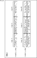
本技術を適用した物理層フレームは、1つのフレーム同期シンボル(FSS:Frame Sync Symbol)と、1以上のP1シンボル(P1:Preamble 1 Symbol(s))と、1以上のP2シンボル(P2:Preamble 2 Symbol(s))と、1以上のデータ(Data)から構成される。
A physical layer frame to which this technology is applied consists of one frame synchronization symbol (FSS: Frame Sync Symbol), one or more P1 symbols (P1:
フレーム同期シンボル(FSS)は、物理層フレームの先頭に挿入される。なお、フレーム同期シンボル(FSS)は、ロバストに構成することができる。 A frame synchronization symbol (FSS) is inserted at the beginning of the physical layer frame. Note that the frame sync symbol (FSS) can be robustly configured.
P1シンボル(P1)は、第1プリアンブル(Preamble 1)である。また、P2シンボル(P2)は、第2プリアンブル(Preamble 2)である。 The P1 symbol (P1) is the first preamble (Preamble 1). Also, the P2 symbol (P2) is the second preamble (Preamble 2).
ここで、例えば、フレーム同期シンボル(FSS)とP1シンボル(P1)は、ATSC3.0で規定される物理層フレームを構成するブートストラップ(Bootstrap)に相当し、P2シンボル(P2)は、プリアンブル(Preamble)に相当している(例えば、下記の非特許文献2参照)。
Here, for example, the frame synchronization symbol (FSS) and the P1 symbol (P1) correspond to the bootstrap that constitutes the physical layer frame specified in ATSC 3.0, and the P2 symbol (P2) corresponds to the preamble ( Preamble) (for example, see
非特許文献2:ATSC Standard:A/321, System Discovery and Signaling Non-Patent Document 2: ATSC Standard: A/321, System Discovery and Signaling
P1シンボル(P1)とP2シンボル(P2)は、物理層のシグナリング(L1シグナリング)を含む。ここでは、P1シンボル(P1)のシグナリングを、P1シグナリングと称する。また、P2シンボル(P2)のシグナリングを、P2シグナリングと称する。 The P1 symbol (P1) and the P2 symbol (P2) contain physical layer signaling (L1 signaling). Signaling of P1 symbols (P1) is referred to herein as P1 signaling. Also, signaling of P2 symbols (P2) is referred to as P2 signaling.
また、P2シグナリングは、固定長部分のL1-Basic(以下、L1Bシグナリングともいう)と、可変長部分のL1-Detail(以下、L1Dシグナリングともいう)とに分けることができる。なお、P1シグナリングとP2シグナリングの詳細は、後述する。 In addition, P2 signaling can be divided into a fixed-length portion of L1-Basic (hereinafter also referred to as L1B signaling) and a variable-length portion of L1-Detail (hereinafter also referred to as L1D signaling). Details of P1 signaling and P2 signaling will be described later.
データ(Data)は、複数のデータシンボル(Data Symbol)から構成される。なお、データ(Data)には、必要に応じて、フレームの境界を示すバウンダリシンボル(BS:Boundary Symbol)が配置される。 Data is composed of a plurality of data symbols. In addition, a boundary symbol (BS: Boundary Symbol) indicating a frame boundary is arranged in the data (Data), if necessary.
本技術を適用した物理層フレームは、以上のように構成することができる。 A physical layer frame to which the present technology is applied can be configured as described above.
なお、図4に示した物理層フレームにおいては、例えば、フレーム同期シンボル(FSS)とP1シンボル(P1)は、上記の非特許文献2に開示されているシンボル(に類似するシンボル)とし、P2シンボル(P2)とデータ(データシンボル)は、OFDMシンボルとすることができる。ここで、OFDM(Orthogonal Frequency Division Multiplexing)(直交周波数分割多重)では、伝送帯域内に多数の直交するサブキャリア(副搬送波)が設けられ、デジタル変調が行われる。
Note that in the physical layer frame shown in FIG. 4, for example, the frame synchronization symbol (FSS) and the P1 symbol (P1) are the symbols (symbols similar to) disclosed in
また、図4に示した物理層フレームの構成の概念は、時分割多重化方式(TDM)、周波数分割多重化方式(FDM)、又は階層分割多重化方式(LDM)のいずれの多重化の方式を採用した場合においても同様である。以下、これらの多重化の方式ごとに、物理層フレームの構成の詳細について説明する。 In addition, the concept of the configuration of the physical layer frame shown in FIG. The same is true when adopting The details of the configuration of the physical layer frame will be described below for each of these multiplexing schemes.
(1)時分割多重化方式(TDM)の物理層フレームの構成 (1) Time division multiplexing (TDM) physical layer frame structure
(第1の構成例)
図5は、時分割多重化方式(TDM)の場合の物理層フレームの第1の構成例を示す図である。
(First configuration example)
FIG. 5 is a diagram showing a first configuration example of a physical layer frame in the case of time division multiplexing (TDM).
時分割多重化方式(TDM)は、複数の放送信号を時間的に配列して1つの伝送路で伝送を行うことができるようにする多重化の方式である。 Time-division multiplexing (TDM) is a multiplexing method that arranges a plurality of broadcast signals in time so that they can be transmitted over a single transmission line.
図5においては、図中の左側から右側に向かう方向を周波数(Freq)の方向とし、図中の上側から下側に向かう方向を時間(Time)の方向としたときにおける、時分割多重化方式(TDM)を用いた場合の物理層フレームの構成を表している。 In FIG. 5, the direction from left to right in the figure is the direction of frequency (Freq), and the direction from top to bottom in the figure is the direction of time (Time). (TDM) is used to represent the structure of a physical layer frame.
図5において、物理層フレームは、時系列で伝送されるが、各物理層フレームの先頭には、フレーム同期シンボル(FSS)が挿入される。ここでは、時系列で伝送される複数の物理層フレームのうち、物理層フレームn(Frame n)の構成を代表して説明する。 In FIG. 5, physical layer frames are transmitted in time sequence, and a frame synchronization symbol (FSS) is inserted at the beginning of each physical layer frame. Here, among a plurality of physical layer frames transmitted in time series, the configuration of a physical layer frame n (Frame n) will be described as a representative.
図5の物理層フレームnは、フレーム同期シンボル(FSS)、P1シンボル(P1)、P2シンボル(P2)、フレーム(Frame)、及びバウンダリシンボル(BS)から構成される。物理層フレームnにおいては、P1シンボルとP2シンボル(のL1シグナリング)を取得した後に、それに続いたフレームを取得することが可能となる。 A physical layer frame n in FIG. 5 consists of a frame synchronization symbol (FSS), a P1 symbol (P1), a P2 symbol (P2), a frame (Frame), and a boundary symbol (BS). In physical layer frame n, after acquiring (the L1 signaling of) the P1 and P2 symbols, it is possible to acquire the subsequent frames.
また、図5の物理層フレームnにおいては、データシンボルとしてのフレーム(Frame)と、バウンダリシンボル(BS)が、データ(Data)に相当している。ここで、バウンダリシンボルは、フレームの終端に挿入されるシンボルを表している。 In addition, in the physical layer frame n in FIG. 5, a frame (Frame) as a data symbol and a boundary symbol (BS) correspond to data (Data). Here, the boundary symbol represents a symbol inserted at the end of the frame.
なお、図5においては、複数の物理層フレームのうち、物理層フレームnの構成を代表して説明したが、物理層フレームn+1などの他の物理層フレームも同様に構成され、時系列で伝送されることになる。 Note that, in FIG. 5, the configuration of the physical layer frame n among the plurality of physical layer frames has been described as a representative, but other physical layer frames such as the physical layer frame n+1 are configured in the same manner. will be transmitted in
(第2の構成例)
図6は、時分割多重化方式(TDM)の場合の物理層フレームの第2の構成例を示す図である。
(Second configuration example)
FIG. 6 is a diagram showing a second configuration example of a physical layer frame in the case of time division multiplexing (TDM).
図6において、物理層フレームnは、図5の物理層フレームnと比べて、1つのフレーム(Frame)の代わりに、1以上のサブフレーム(SubFrame)が配置される点が異なっている。図6の物理層フレームnには、サブフレームn(SubFrame n)と、サブフレームn+1(SubFrame n+1)の2つのサブフレームが配置されている。 In FIG. 6, physical layer frame n differs from physical layer frame n in FIG. 5 in that one or more subframes (SubFrame) are arranged instead of one frame (Frame). Two subframes, a subframe n (SubFrame n) and a subframe n+1 (SubFrame n+1), are arranged in the physical layer frame n of FIG.
図6の物理層フレームnにおいては、P1シンボルとP2シンボル(のL1シグナリング)を取得した後に、それに続いたサブフレームnとサブフレームn+1を取得することが可能となる。 In the physical layer frame n of FIG. 6, after acquiring (the L1 signaling of) the P1 and P2 symbols, it is possible to acquire the subsequent subframes n and subframe n+1.
ここで、図6の物理層フレームnにおいて、2以上のサブフレームが配置される場合には、サブフレームごとに、例えば、FFTサイズやガードインターバル長、パイロットパターンなどの変調パラメータを変更することができる。 Here, when two or more subframes are arranged in the physical layer frame n of FIG. can.
また、各サブフレームには、当該サブフレームの始端と終端に挿入されるシンボルを表すサブフレームバウンダリシンボル(Subframe Boundary Symbol)が挿入される。そして、物理層フレームnにおいては、データシンボルとしてのサブフレームと、サブフレームバウンダリシンボルとが、データ(Data)に相当している。 In each subframe, subframe boundary symbols representing symbols to be inserted at the beginning and end of the subframe are inserted. In the physical layer frame n, a subframe as a data symbol and a subframe boundary symbol correspond to data (Data).
時分割多重化方式(TDM)を用いた場合の物理層フレームは、以上のように構成することができる。 A physical layer frame using time division multiplexing (TDM) can be configured as described above.
(2)周波数分割多重化方式(FDM)の物理層フレームの構成 (2) Structure of physical layer frame of frequency division multiplexing (FDM)
(フレーム構成例)
図7は、周波数分割多重化方式(FDM)の場合の物理層フレームの構成例を示す図である。
(Example of frame configuration)
FIG. 7 is a diagram showing a configuration example of a physical layer frame in the case of frequency division multiplexing (FDM).
周波数分割多重化方式(FDM)は、複数の放送信号を伝送する周波数帯域を分割して1つの伝送路で伝送を行うことができるようにする多重化の方式である。 Frequency division multiplexing (FDM) is a multiplexing method that divides a frequency band for transmitting a plurality of broadcast signals so that the signals can be transmitted over a single transmission line.
図7においては、図中の左側から右側に向かう方向を周波数(Freq)の方向とし、図中の上側から下側に向かう方向を時間(Time)の方向としたときにおける、周波数分割多重化方式(FDM)を用いた場合の物理層フレームの構成を表している。 In FIG. 7, the direction from left to right in the figure is the direction of frequency (Freq), and the direction from top to bottom in the figure is the direction of time (Time). 1 shows the configuration of a physical layer frame when using (FDM).
図7において、物理層フレームは、時系列で伝送されるが、各物理層フレームの先頭には、フレーム同期シンボル(FSS)が挿入され、さらに、それに続いてP1シンボル(P1)が挿入される。 In FIG. 7, physical layer frames are transmitted in chronological order. At the beginning of each physical layer frame, a frame synchronization symbol (FSS) is inserted, followed by a P1 symbol (P1). .
また、周波数分割多重化方式(FDM)を用いる場合には、所定の周波数帯域(例えば6MHz)が、複数のセグメントに周波数分割される。そして、1又は複数のセグメントをまとめることで、階層が構成される。例えば、図7においては、35セグメントに周波数分割して、図中の中央の9セグメントにより、階層A(Layer A)が構成され、左右の残りのセグメントにより、階層B(Layer B)が構成される。 Also, when using frequency division multiplexing (FDM), a predetermined frequency band (eg, 6 MHz) is frequency-divided into a plurality of segments. A hierarchy is constructed by grouping one or a plurality of segments. For example, in FIG. 7, the frequency is divided into 35 segments, and the middle 9 segments in the figure constitute a layer A (Layer A), and the left and right remaining segments constitute a layer B (Layer B). be.
図7の物理層フレームnにおいては、階層Aと階層Bの階層ごとに、P2シンボル(P2)と、データシンボルとしてのフレーム(Frame)と、バウンダリシンボル(BS)が配置される。 In the physical layer frame n of FIG. 7, a P2 symbol (P2), a frame (Frame) as a data symbol, and a boundary symbol (BS) are arranged for each layer of layer A and layer B. FIG.
ここで、図8には、図7の物理層フレームの構成の詳細を示している。図8においては、階層Aと階層Bの階層ごとのP2シンボル、データシンボル、及びバウンダリシンボルが、図中の四角で表したセグメント単位で示されている。 Here, FIG. 8 shows details of the configuration of the physical layer frame in FIG. In FIG. 8, P2 symbols, data symbols, and boundary symbols for each hierarchy of hierarchy A and hierarchy B are shown in units of segments represented by squares in the figure.
すなわち、図8では、周波数分割多重化方式(FDM)を用いることで、例えば、35セグメントに周波数分割されている場合に、中央の階層Aは、9セグメントから構成され、左右の階層Bは、残りの26セグメントから構成されている。なお、図中の四角で表した各セグメントは、同一のサブキャリアの数で構成される。 That is, in FIG. 8, by using frequency division multiplexing (FDM), for example, when the frequency is divided into 35 segments, the middle layer A is composed of 9 segments, and the left and right layers B are It consists of the remaining 26 segments. Each segment represented by a square in the figure is composed of the same number of subcarriers.
周波数分割多重化方式(FDM)を用いた場合の物理層フレームは、以上のように構成することができる。 A physical layer frame using frequency division multiplexing (FDM) can be configured as described above.
(3)階層分割多重化方式(LDM)の物理層フレームの構成 (3) Composition of physical layer frame of hierarchical division multiplexing (LDM)
(フレーム構成例)
図9は、階層分割多重化方式(LDM)の場合の物理層フレームの構成例を示す図である。
(Example of frame configuration)
FIG. 9 is a diagram showing a configuration example of a physical layer frame in the case of hierarchical division multiplexing (LDM).
階層分割多重化方式(LDM)は、複数の放送信号を異なる階層電力に分割して1つの伝送路で伝送を行うことができるようにする多重化の方式である。 Hierarchical division multiplexing (LDM) is a multiplexing scheme that divides a plurality of broadcast signals into different hierarchical powers for transmission over a single transmission path.
図9においては、xyzの3次元により、階層分割多重化方式(LDM)を用いた場合の物理層フレームの構成を表している。ただし、図9では、図中のx方向を、電力(Power)の方向とし、図中のy方向を、周波数(Freq)の方向とし、図中のz方向を、時間(Time)の方向としている。 In FIG. 9, three dimensions of xyz represent the structure of a physical layer frame when using the hierarchical division multiplexing (LDM). However, in FIG. 9, the x direction in the figure is the direction of power, the y direction in the figure is the direction of frequency (Freq), and the z direction in the figure is the direction of time. there is
図9において、物理層フレームは、時系列で伝送されるが、各物理層フレームの先頭には、フレーム同期シンボル(FSS)が挿入され、さらに、それに続いてP1シンボル(P1)が挿入される。 In FIG. 9, physical layer frames are transmitted in chronological order. At the beginning of each physical layer frame, a frame synchronization symbol (FSS) is inserted, followed by a P1 symbol (P1). .
また、階層分割多重化方式(LDM)を用いる場合には、異なる送信電力となる階層ごとに、P2シンボル(P2)、データシンボルとしてのフレーム(Frame)、及びバウンダリシンボル(BS)が配置される。例えば、図9の物理層フレームnにおいては、階層k(Layer k)と階層k+1(Layer k+1)の2つの階層ごとに、P2シンボルと、データシンボルと、バウンダリシンボルがそれぞれ配置されている。 Also, when using a hierarchical division multiplexing (LDM), P2 symbols (P2), frames as data symbols (Frame), and boundary symbols (BS) are arranged for each layer with different transmission power. . For example, in the physical layer frame n of FIG. 9, P2 symbols, data symbols, and boundary symbols are arranged for each of two layers, layer k (Layer k) and layer k+1 (Layer k+1). ing.
階層分割多重化方式(LDM)を用いた場合の物理層フレームは、以上のように構成することができる。 A physical layer frame using hierarchical division multiplexing (LDM) can be configured as described above.
なお、本明細書の説明では、周波数分割多重化方式(FDM)と、階層分割多重化方式(LDM)において、同一の「階層(Layer)」の用語を用いているが、これらの「階層」の意味は、技術的には異なるものである。ここで、本明細書の説明においては、どちらの方式の階層であるかが明らかである場合には、特に区別せずに、「階層」の用語を用いる。一方で、特に、「階層」の用語を区別する必要がある場合には、周波数分割多重化方式(FDM)の階層を、「FDM階層」と記述し、階層分割多重化方式(LDM)の階層を、「LDM階層」と記述するものとする。 In the description of this specification, the same term "layer" is used for frequency division multiplexing (FDM) and hierarchical division multiplexing (LDM). are technically different. Here, in the description of this specification, the term "hierarchy" is used without particular distinction when it is clear which of the hierarchies is which. On the other hand, when it is necessary to specifically distinguish between the terms "hierarchy", the frequency division multiplexing (FDM) hierarchy is described as the "FDM hierarchy" and the hierarchical division multiplexing (LDM) hierarchy. shall be described as the "LDM hierarchy".
(4)フレーム同期シンボル(FSS)とP1シンボル(P1)の構成 (4) Configuration of Frame Synchronization Symbol (FSS) and P1 Symbol (P1)
次に、図10乃至図22を参照して、物理層フレームにおける、フレーム同期シンボル(FSS)とP1シンボル(P1)の構成について説明する。 Next, configurations of a frame synchronization symbol (FSS) and a P1 symbol (P1) in a physical layer frame will be described with reference to FIGS. 10 to 22. FIG.
(現状のFSSとP1の構成)
図10は、現状のフレーム同期シンボル(FSS)とP1シンボル(P1)の構成を示す図である。
(Current configuration of FSS and P1)
FIG. 10 is a diagram showing the configuration of the current frame synchronization symbol (FSS) and P1 symbol (P1).
図10に示したCAB構造とBCA構造は、ATSC3.0で規定されるブートストラップ(Bootstrap)の構成に相当するものである(例えば、上記の非特許文献2参照)。ここでは、フレーム同期シンボル(FSS)は、CAB構造からなる一方で、P1シンボル(P1)は、BCA構造からなる。すなわち、ATSC3.0では、1つの物理層フレームにおいて、1つのフレーム同期シンボル(FSS)と、3つのP1シンボル(P1)を含むことが規定されている。
The CAB structure and BCA structure shown in FIG. 10 correspond to the bootstrap structure defined by ATSC 3.0 (for example, see
ただし、図10のフレーム同期シンボル(FSS)のCAB構造では、Cの部分のサンプル(Sample)は、520とされ、Aの部分のサンプルは、2048とされ、Bの部分のサンプルは、504とされる。同様に、図10のP1シンボル(P1)のBCA構造では、Bの部分のサンプルは、504とされ、Cの部分のサンプルは、520とされ、Aの部分のサンプルは、2048とされる。 However, in the CAB structure of the frame synchronization symbol (FSS) in FIG. be done. Similarly, in the BCA structure of the P1 symbol (P1) of FIG. 10, the B portion samples are 504, the C portion samples are 520, and the A portion samples are 2048 samples.
(本技術のFSSとP1の構成)
図11は、本技術のフレーム同期シンボル(FSS)とP1シンボル(P1)の構成の概要を示す図である。
(Configuration of FSS and P1 of this technology)
FIG. 11 is a diagram showing an overview of the configuration of the frame synchronization symbol (FSS) and P1 symbol (P1) of this technology.
図11において、フレーム同期シンボル(FSS)のCAB構造では、C,A,Bの部分のサンプルをそれぞれ、520g,2048g,504gとした場合に、本技術の構成では、主に、g = 0.5となるようにする。一方で、P1シンボル(P1)のBCA構造においても、B,C,Aの部分のサンプルをそれぞれ、504g,520g,2048gとした場合に、本技術の構成では、主に、g = 0.5となるようにする。 In FIG. 11, in the CAB structure of the frame synchronization symbol (FSS), when the samples of the C, A, and B portions are 520g, 2048g, and 504g, respectively, in the configuration of this technology, g = 0.5 and be. On the other hand, even in the BCA structure of the P1 symbol (P1), when the samples of the B, C, and A portions are 504g, 520g, and 2048g, respectively, g = 0.5 is mainly obtained in the configuration of the present technology. make it
すなわち、g = 0.5とすることで、フレーム同期シンボル(FSS)とP1シンボル(P1)のシンボルの長さを半分にすることができるため、物理層フレームにおいて、高効率を実現することができる。 That is, by setting g = 0.5, the symbol length of the frame synchronization symbol (FSS) and the P1 symbol (P1) can be halved, so that high efficiency can be achieved in the physical layer frame.
具体的には、フレーム同期シンボル(FSS)のCAB構造では、Cの部分のサンプルを、260とし、Aの部分のサンプルを、1024とし、Bの部分のサンプルを、252とすることができる。同様に、P1シンボル(P1)のBCA構造では、Bの部分のサンプルを、252とし、Cの部分のサンプルを、260とし、Aの部分のサンプルを、1024とすることができる。 Specifically, in the frame sync symbol (FSS) CAB structure, the C portion may have 260 samples, the A portion may have 1024 samples, and the B portion may have 252 samples. Similarly, in the BCA structure of the P1 symbol (P1), the B portion may have 252 samples, the C portion may have 260 samples, and the A portion may have 1024 samples.
また、本技術の構成では、ATSC3.0の構成と比べて、P1シンボルの数を、3つから2つに減らすことで、1つの物理層フレームにおいて、1つのフレーム同期シンボル(FSS)と、2つのP1シンボル(P1)を含むようにする。すなわち、本技術の構成では、ATSC3.0の構成と比べて、効率を、3/4にする。 In addition, in the configuration of this technology, the number of P1 symbols is reduced from three to two compared to the configuration of ATSC3.0, so that in one physical layer frame, one frame synchronization symbol (FSS) and Let it contain two P1 symbols (P1). That is, in the configuration of this technology, the efficiency is 3/4 compared to the configuration of ATSC3.0.
図12には、フレーム同期シンボル(FSS)とP1シンボル(P1)の構成として、上段に、ATSC3.0の構成を示す一方で、下段に、本技術の構成を示している。 In FIG. 12 , as the configurations of the frame synchronization symbol (FSS) and the P1 symbol (P1), the upper part shows the configuration of ATSC 3.0, while the lower part shows the configuration of this technology.
図12において、下段の本技術の構成では、上段のATSC3.0の構成と比べて、フレーム同期シンボル(FSS)とP1シンボル(P1)のシンボルの長さを半分にし、さらに、P1シンボルの数を、3つから2つに減らしている。そのため、下段の本技術の構成は、上段のATSC3.0の構成と比べれば、伝送時間を、3/8(1/2 × 3/4)の時間に短縮することができる。 In FIG. 12 , in the configuration of this technology in the lower part, compared to the configuration of ATSC3.0 in the upper part, the symbol lengths of the frame synchronization symbol (FSS) and the P1 symbol (P1) are halved, and the number of P1 symbols is is reduced from three to two. Therefore, the configuration of this technology in the lower part can reduce the transmission time to 3/8 (1/2 × 3/4) compared to the configuration of ATSC3.0 in the upper part.
ここで、図13には、gの値と、FFTサイズ、サンプル(Samples)、最大伝送速度(Max bps)、及びロバスト伝送速度(Robust bps)との関係を示している。 Here, FIG. 13 shows the relationship between the value of g, FFT size, samples, maximum transmission rate (Max bps), and robust transmission rate (Robust bps).
図13においては、gの値に応じて、FFTサイズ、サンプル、最大伝送速度、及びロバスト伝送速度の値が増減する。上述したように、本技術の構成では、g = 0.5として、FTTサイズ = 1024,サンプル = 1536,最大伝送速度 = 10bps,ロバスト伝送速度 = 6bps又は7bpsとすることで、ATSC3.0の構成(g = 1.0)と比べて、効率を良くすることができる。 In FIG. 13, the values of FFT size, samples, maximum transmission rate, and robust transmission rate increase or decrease according to the value of g. As described above, in the configuration of this technology, g = 0.5, FTT size = 1024, samples = 1536, maximum transmission rate = 10 bps, robust transmission rate = 6 bps or 7 bps, ATSC 3.0 configuration (g = 1.0).
なお、ロバスト伝送速度であるが、論理的には最大10bpsは可能であるが、チャネルのノイズなどによって、相関が十分に取れなくなる場合があるので、実際には、バックオフ(back-off)を持って、3bps又は4bpsで運用することになる。なお、ATSC3.0の構成では、論理的には最大11bpsとなるが、実際には、8bpsで運用を行うことになる。一方で、本技術の構成では、論理的には最大10bpsとなるところ、例えば、6bpsで運用を行うようにすることができる。 In terms of robust transmission speed, theoretically a maximum of 10bps is possible, but there are cases where sufficient correlation cannot be obtained due to channel noise, etc. In practice, back-off is used. It will be operated at 3bps or 4bps. In the configuration of ATSC3.0, the logical maximum is 11bps, but in practice, it will be operated at 8bps. On the other hand, in the configuration of the present technology, logically, the maximum is 10 bps, but for example, it is possible to operate at 6 bps.
また、本技術の発明者は、gの値として、g = 0.5が好適であることを証明するために、図13に示したFFTサイズごとに、SNR(Symbol to Noise Ratio)を得るためのシミュレーションを行った。このシミュレーション結果を、図14乃至図18に示している。 In addition, the inventor of the present technology performed a simulation for obtaining an SNR (Symbol to Noise Ratio) for each FFT size shown in FIG. 13 in order to prove that g = 0.5 is suitable as the value of g did The simulation results are shown in FIGS. 14 to 18. FIG.
なお、このシミュレーションでは、受信装置30が、チャネルに割り当てられた周波数帯域(例えば6MHz)の全帯域を受信する場合を想定している。また、図14乃至図18においては、横軸がSNR(Symbol to Noise Ratio)を表し、縦軸がBLER(Block Error Rate)を表している。
Note that this simulation assumes that the receiving
また、図14乃至図18において、シミュレーションの結果として異なる線種で表した[a,b,c]のaは、フレーム同期シンボル(FSS)のビット数を表し、a以外のbやc等は、P1シンボル(P1)のビット数を表している。フレーム同期シンボル(FSS)は、情報がないので、すべて0ビットとされる。また、P1シンボル(P1)のビット数は、2~12ビット等としている。 In FIGS. 14 to 18, a in [a, b, c] represented by different line types as a result of simulation represents the number of bits of the frame synchronization symbol (FSS), and b, c, etc. other than a are , representing the number of bits in the P1 symbol (P1). The Frame Synchronization Symbol (FSS) has no information and is therefore all 0 bits. Also, the number of bits of the P1 symbol (P1) is 2 to 12 bits.
図14は、FFTサイズ = 512の場合のシミュレーション結果を示している。図14のシミュレーション結果においては、BLER = 1.0×10⁻³(1.0E-03)のとき、SNR = -6dBとなる。 FIG. 14 shows simulation results for FFT size=512. In the simulation result of FIG. 14, SNR=-6dB when BLER=1.0×10⁻³ (1.0E-03).
図15は、FFTサイズ = 1024の場合のシミュレーション結果を示している。図15のシミュレーション結果においては、BLER = 1.0×10⁻³(1.0E-03)のとき、SNR = -7.6dBとなる。 FIG. 15 shows simulation results for FFT size=1024. In the simulation result of FIG. 15, SNR=-7.6 dB when BLER=1.0×10⁻³ (1.0E-03).
図16は、FFTサイズ = 2048の場合のシミュレーション結果を示している。図16のシミュレーション結果においては、BLER = 1.0×10⁻³(1.0E-03)のとき、SNR = -9.6dBとなる。 FIG. 16 shows simulation results for FFT size=2048. In the simulation result of FIG. 16, SNR=-9.6 dB when BLER=1.0×10⁻³ (1.0E-03).
図17は、FFTサイズ = 4096の場合のシミュレーション結果を示している。図17のシミュレーション結果においては、BLER = 1.0×10⁻³(1.0E-03)のとき、SNR = -10.8dBとなる。 FIG. 17 shows simulation results for FFT size=4096. In the simulation result of FIG. 17, SNR=-10.8 dB when BLER=1.0×10⁻³ (1.0E-03).
図18は、FFTサイズ = 8192の場合のシミュレーション結果を示している。図18のシミュレーション結果においては、BLER = 1.0×10⁻³(1.0E-03)のとき、SNR = -12.5dBとなる。 FIG. 18 shows simulation results for FFT size=8192. In the simulation result of FIG. 18, SNR=-12.5 dB when BLER=1.0×10⁻³ (1.0E-03).
ここで、ATSC3.0の構成は、g = 1.0,すなわち、FFTサイズ = 2048の場合のシミュレーション結果(図16)に相当するので、SNR = -9.6dBとなる。一方で、本技術の構成は、g = 0.5,すなわち、FFTサイズ = 1024の場合のシミュレーション結果(図15)に相当するので、SNR = -7.6dBとなる。 Here, the ATSC3.0 configuration corresponds to the simulation result (FIG. 16) for g=1.0, that is, FFT size=2048, so SNR=-9.6 dB. On the other hand, the configuration of this technology corresponds to the simulation result (FIG. 15) for g=0.5, that is, FFT size=1024, resulting in SNR=-7.6 dB.
そして、SNRとしては、通常、-7.6dB程度であれば、十分な値であり、-9.6dBまでは必要ない。換言すれば、ATSC3.0の構成で用いられる、g = 1.0の場合にはオーバースペックであり、g = 0.5で、十分な性能が得られる。そのため、本技術の構成では、g = 0.5が好適であるとしている。 As for the SNR, an SNR of about -7.6 dB is usually a sufficient value, and an SNR of up to -9.6 dB is not necessary. In other words, g = 1.0, which is used in the configuration of ATSC 3.0, is over-specification, and g = 0.5 provides sufficient performance. Therefore, in the configuration of the present technology, it is said that g = 0.5 is suitable.
ただし、ここでは、伝送時間の短縮の観点から、g = 0.5が好適であるとして説明をしたが、本技術の物理層フレームの構成では、g = 0.25,1.00,2.00,4.00など、gの値として、0.5以外の他の値を用いるようにしてもよい。 However, here, from the viewpoint of shortening the transmission time, it was explained that g = 0.5 is preferable. , other values than 0.5 may be used.
また、多重化の方式として、周波数分割多重化方式(FDM)を用いる場合、受信装置30は、フレーム同期シンボル(FSS)とP1シンボル(P1)を部分帯域で受信することになる。例えば、図19に示すように、周波数分割多重化方式(FDM)を用いる場合には、チャネルに割り当てられた所定の周波数帯域(例えば6MHz)が、複数のセグメントに周波数分割される。
Also, when frequency division multiplexing (FDM) is used as the multiplexing method, receiving
図19の例では、横方向を周波数としたときに、周波数上限と周波数下限との間の周波数帯域(例えば6MHz)内の、図中の四角で表したセグメントにより、階層(FDM階層)が構成されることを示している。図19においては、35セグメントに周波数分割されている。 In the example of FIG. 19, when the horizontal direction is frequency, a hierarchy (FDM hierarchy) is configured by segments represented by squares in the figure within a frequency band (for example, 6 MHz) between the upper frequency limit and the lower frequency limit. It indicates that In FIG. 19, the frequency is divided into 35 segments.
ここでは、35個のセグメントのうち、図中の中央の1セグメントを、セグメント#0として、その左右のセグメントを、セグメント#1,#2とし、さらに、その左右のセグメントを、セグメント#3,#4とすることを繰り返していくと、図中の最も左側(周波数下限側)の1セグメントが、セグメント#33となり、図中の最も右側(周波数上限側)の1セグメントが、セグメント#34となる。
Here, among the 35 segments, the center segment in the figure is
また、1又は複数のセグメントをまとめることで、階層が構成される。図19においては、セグメント#0乃至#8の9セグメントにより、階層A(Layer A)が構成される。また、セグメント#10,#12,・・・,#32,#34の13セグメントと、セグメント#9,#11,・・・,#31,#33の13セグメントとの合計26セグメントにより、階層B(Layer B)が構成される。
Also, a hierarchy is configured by grouping one or more segments. In FIG. 19, a hierarchy A (Layer A) is composed of nine
このように、1又は複数のセグメントから階層が構成され、それらの階層ごとに、例えば、異なる放送サービスのデータを伝送することができる。例えば、受信装置30は、階層Aで伝送される放送サービスのデータを受信する場合、部分帯域フィルタ(図19)により、階層Aの周波数帯域のみを受信することになる。
In this way, one or more segments form a hierarchy, each of which can carry, for example, data of different broadcast services. For example, when the receiving
すなわち、受信装置30では、チャネルに割り当てられた周波数帯域の全帯域のうち、階層Aに対応した部分帯域のみが受信され、フレーム同期シンボル(FSS)とP1シンボル(P1)は、部分帯域で受信される。つまり、周波数帯域の全帯域に対し、階層Aに対応した部分帯域は、9/35の帯域とされる。
That is, the receiving
ここで、本技術の発明者は、階層Aに対応した部分帯域を、全帯域の9/35の帯域(約1/4の帯域)とした場合でも、gの値として、g = 0.5が好適であることを証明するために、FFTサイズ = 1024の場合に、SNRを得るためのシミュレーションを行った。このシミュレーション結果を、図20に示している。 Here, the inventor of the present technology prefers g = 0.5 as the value of g even when the partial band corresponding to layer A is 9/35 of the total band (approximately 1/4 band). In order to prove that , a simulation was performed to obtain the SNR when FFT size = 1024. This simulation result is shown in FIG.
なお、図20においては、上述した図14乃至図18と同様に、横軸がSNRを表し、縦軸がBLERを表している。また、図20には、5パターンのシミュレーション結果を示している。すなわち、異なる線種で表した[a,b,c]のa,b,cは、フレーム同期シンボル(FSS)のビット数、1つ目のP1シンボル(P1)のビット数、2つ目のP1シンボル(P1)のビット数をそれぞれ表している。 20, the horizontal axis represents SNR, and the vertical axis represents BLER, as in FIGS. 14 to 18 described above. In addition, FIG. 20 shows simulation results of five patterns. That is, a, b, c of [a, b, c] represented by different line types are the number of bits of the frame synchronization symbol (FSS), the number of bits of the first P1 symbol (P1), and the number of bits of the second P1 symbol (P1). Each represents the number of bits of the P1 symbol (P1).
フレーム同期シンボル(FSS)は、情報がないので、すべて0ビットとされる。また、P1シンボル(P1)のビット数は、4~7ビットとしている。つまり、例えば、[0,5,5]は、0ビットのFSS,5ビットのP1,5ビットのP1の合計10ビットの情報とされる。同様に、[0,5,4]は、9ビットの情報、[0,4,4]は、8ビットの情報、[0,6,6]は、12ビットの情報、[0,7,7]は、14ビットの情報となる。 The Frame Synchronization Symbol (FSS) has no information and is therefore all 0 bits. Also, the number of bits of the P1 symbol (P1) is 4 to 7 bits. That is, for example, [0, 5, 5] is 0-bit FSS, 5-bit P1, and 5-bit P1, a total of 10 bits of information. Similarly, [0,5,4] is 9-bit information, [0,4,4] is 8-bit information, [0,6,6] is 12-bit information, [0,7, 7] is 14-bit information.
図20の各シミュレーション結果においては、BLER = 1.0×10⁻³(1.0E-03)のとき、SNR = -4dB程度が得られる。すなわち、g = 0.5の場合について、部分帯域(9/35の帯域)のシミュレーション結果(図20)を、上述した全帯域のシミュレーション結果(図15)と比べれば、BLER = 1.0×10⁻³(1.0E-03)のときのSNRが、-7.6dBから、-4dB程度に低下している。 In each simulation result of FIG. 20, when BLER=1.0×10 −3 (1.0E-03), SNR=about −4 dB is obtained. That is, when g = 0.5, BLER = 1.0 × 10⁻³ ( 1.0E-03), the SNR drops from -7.6dB to about -4dB.
しかしながら、SNRとしては、通常、-4dB程度であれば、許容範囲内の値であり、十分な性能が得られる。そのため、階層Aに対応した部分帯域を、全帯域の9/35の帯域とした場合でも、gの値として、g = 0.5が好適であると言える。 However, an SNR of about -4 dB is usually within the allowable range and sufficient performance can be obtained. Therefore, even if the partial band corresponding to layer A is 9/35 of the total band, it can be said that g=0.5 is suitable as the value of g.
また、上述した各種のシミュレーション結果に基づいて、ロバスト性を考慮に入れると、1シンボルを、6ビットとすることができる。ただし、実際には、4ビットのバックオフを持つことで、最大10ビットとした上で、6ビットで運用することができる。 Also, based on the various simulation results described above, taking robustness into consideration, one symbol can be set to 6 bits. However, in reality, by having a 4-bit backoff, it is possible to operate at 6 bits with a maximum of 10 bits.
一方で、送信側の送信装置20から、受信側の受信装置30に送信すべき情報を考慮すれば、6ビットでは不足してしまうため、2つのP1シンボルが必要となる。これにより、12ビット(6ビット×2)のP1シンボルで、情報を送ることが可能となる。このようなP1シンボルの構成を、図21に示している。
On the other hand, considering the information to be transmitted from the transmitting
すなわち、図21において、1つの物理層フレームは、1つのフレーム同期シンボル(FSS)と、2つのP1シンボルを含んで構成される。このように、効率の観点だけでなく、1シンボル当たりのビット数からも、2つのP1シンボルを用いることが好適であることが分かる。なお、図21には、FFTサイズ = 1024(1K)の構成と、FFTサイズ = 2048(2K)の構成を示しているが、FFTサイズ = 1024の構成で、十分な性能を得られることは先に述べた通りである。 That is, in FIG. 21, one physical layer frame includes one frame synchronization symbol (FSS) and two P1 symbols. Thus, it can be seen that using two P1 symbols is preferable not only from the viewpoint of efficiency but also from the number of bits per symbol. Fig. 21 shows a configuration with FFT size = 1024 (1K) and a configuration with FFT size = 2048 (2K). It is as described in
以上をまとめると、図22のように表すことができる。図22には、FFTサイズ、1シンボル当たりのサンプル(Samples Per sym)、最大伝送速度(Max bps)、ロバスト伝送速度(Robust bps)、シンボル数(#Syms)、最大ビット数(Maxbits)、及びトータルサンプル(Total Samples)の関係を示している。 The above can be summarized as shown in FIG. FIG. 22 shows FFT size, samples per symbol (Samples Per sym), maximum transmission rate (Max bps), robust transmission rate (Robust bps), number of symbols (#Syms), maximum number of bits (Maxbits), and The relation of total samples is shown.
すなわち、本技術の構成では、gの値として、g = 0.5が好適であるとして、FFTサイズ = 1024,1シンボル当たりのサンプル = 1536,最大伝送速度 = 10bps,ロバスト伝送速度 = 6bps,シンボル数 = 3,最大ビット数 = 12ビット(6ビット×2),トータルサンプル数 = 4608(1536×3)とすることができる。 That is, in the configuration of this technology, the value of g is preferably g = 0.5, FFT size = 1024, samples per symbol = 1536, maximum transmission rate = 10 bps, robust transmission rate = 6 bps, number of symbols = 3, maximum number of bits = 12 bits (6 bits x 2), total number of samples = 4608 (1536 x 3).
なお、1シンボル当たりのサンプルは、図12等に示したように、g = 0.5として、フレーム同期シンボル(FSS)とP1シンボル(P1)のシンボルの長さを半分にすることで、1536が得られる。また、シンボル数は、図12等に示したように、1つの物理層フレームにおいて、1つのフレーム同期シンボル(FSS)と、2つのP1シンボル(P1)とすることで、3シンボルとなる。さらに、最大ビット数を12ビットとしているのは、1シンボルを6ビットとした場合に、送信側から受信側に送るべき情報を考慮すると、2つのP1シンボルで12ビットになるからである。 As shown in Fig. 12, 1536 samples per symbol are obtained by setting g = 0.5 and halving the length of the frame synchronization symbol (FSS) and the P1 symbol (P1). be done. Also, as shown in FIG. 12 and the like, the number of symbols is 3 by setting one frame synchronization symbol (FSS) and two P1 symbols (P1) in one physical layer frame. Furthermore, the reason why the maximum number of bits is 12 is that when one symbol is 6 bits, two P1 symbols are 12 bits when considering the information to be sent from the transmitting side to the receiving side.
また、ここで、例えば、サンプリング周波数を、6.912MHzとすれば、FFTサイズ = 1024(1K)の場合、1シンボル当たりの時間が、0.222msとなるので、3シンボルであると、0.666msとなる。一方で、FFTサイズ = 2048(1K)の場合には、サンプリング周波数を、6.912MHzとすれば、1.33msとされる。なお、ここでは、サンプリング周波数として、6.912MHzを用いたが、他のサンプリング周波数を用いるようにしてもよい。 Also, here, for example, if the sampling frequency is 6.912 MHz, and the FFT size = 1024 (1K), the time per symbol is 0.222 ms, so if there are 3 symbols, it will be 0.666 ms. . On the other hand, in the case of FFT size = 2048 (1K), the sampling frequency is 1.33 ms if the sampling frequency is 6.912 MHz. Although 6.912 MHz is used here as the sampling frequency, other sampling frequencies may be used.
(5)P2シンボル(P2)の構成 (5) Configuration of P2 symbol (P2)
次に、図23乃至図27を参照して、物理層フレームのP2シンボルの構成について説明する。なお、P2シンボルの構成は、多重化の方式ごとに異なるので、以下、時分割多重化方式(TDM)、周波数分割多重化方式(FDM)、階層分割多重化方式(LDM)の順に、P2シンボルの構成を説明する。 Next, the configuration of the P2 symbol of the physical layer frame will be described with reference to FIGS. 23 to 27. FIG. Since the structure of the P2 symbol differs depending on the multiplexing method, the P2 symbol is used in the order of time division multiplexing (TDM), frequency division multiplexing (FDM), and hierarchical division multiplexing (LDM). will be explained.
(TDMの場合の構成例)
図23は、時分割多重化方式(TDM)の場合のP2シンボルの構成例を示す図である。
(Configuration example for TDM)
FIG. 23 is a diagram showing a configuration example of a P2 symbol in the case of time division multiplexing (TDM).
P2シンボルは、OFDMシンボルであり、L1Bシグナリングと、L1Dシグナリングを含む。ここで、図23には、1つの物理層フレームにおいて、1つのP2シンボルが配置される場合と、2つのP2シンボルが配置される場合を示している。 A P2 symbol is an OFDM symbol and includes L1B signaling and L1D signaling. Here, FIG. 23 shows a case where one P2 symbol is arranged and a case where two P2 symbols are arranged in one physical layer frame.
1つのP2シンボルが配置される場合には、P2シンボルの先頭から、固定長のL1Bシグナリング(L1-Basic)が配置され、それに続いて、可変長のL1Dシグナリング(L1-Detail)が配置される。また、P2シンボルの残りの部分には、データ(Payload Data)が配置される。 When one P2 symbol is allocated, fixed-length L1B signaling (L1-Basic) is allocated from the beginning of the P2 symbol, followed by variable-length L1D signaling (L1-Detail). . Data (Payload Data) is arranged in the remaining portion of the P2 symbol.
一方で、2つのP2シンボルが配置される場合には、1つ目のP2シンボルの先頭から固定長のL1Bシグナリング(L1-Basic)が配置され、それに続いて、可変長のL1Dシグナリング(L1-Detail)が配置される。ここでは、可変長のL1Dシグナリングが、1つ目のP2シンボル内には収まらないため、そのL1Dシグナリングの残りの部分が、2つ目のP2シンボルに配置される。また、2つ目のP2シンボルの残りの部分には、データ(Payload Data)が配置される。 On the other hand, when two P2 symbols are arranged, fixed-length L1B signaling (L1-Basic) is arranged from the beginning of the first P2 symbol, followed by variable-length L1D signaling (L1- Detail) is placed. Here, the variable length L1D signaling does not fit within the first P2 symbol, so the rest of the L1D signaling is placed in the second P2 symbol. Data (Payload Data) is arranged in the remaining portion of the second P2 symbol.
なお、図6に示したような、物理層フレームにおいて、1以上のサブフレームが配置される構成の場合には、すべてのL1シグナリング(L1BシグナリングとL1Dシグナリングを含む)が、先頭のサブフレームよりも前に配置される。 In addition, as shown in FIG. 6, in the physical layer frame, in the case of a configuration in which one or more subframes are arranged, all L1 signaling (including L1B signaling and L1D signaling) is is placed in front.
(FDMの場合の第1の構成例)
図24は、周波数分割多重化方式(FDM)の場合のP2シンボルの第1の構成例を示す図である。
(First configuration example for FDM)
FIG. 24 is a diagram showing a first configuration example of a P2 symbol in the case of frequency division multiplexing (FDM).
ここで、図24には、周波数分割多重化方式(FDM)を用いることで、階層Aと階層Bが構成されるときに、1つの物理層フレームにおいて、1つのP2シンボルが配置される場合と、2つのP2シンボルが配置される場合を示している。 Here, FIG. 24 shows a case where one P2 symbol is arranged in one physical layer frame when hierarchy A and hierarchy B are configured by using frequency division multiplexing (FDM). , where two P2 symbols are placed.
1つのP2シンボルが配置される場合、P2シンボルでは、階層Aに対応する部分の先頭から、固定長のL1Bシグナリング(L1-Basic)が配置され、それに続いて、可変長のL1Dシグナリング(L1-Detail)が配置される。また、P2シンボルにおいて、階層Aに対応する部分のうち、残りの部分には、データ(Payload Data)が配置される。 When one P2 symbol is allocated, in the P2 symbol, fixed-length L1B signaling (L1-Basic) is allocated from the beginning of the part corresponding to layer A, followed by variable-length L1D signaling (L1-Basic). Detail) is placed. In addition, data (Payload Data) is arranged in the remaining part of the part corresponding to layer A in the P2 symbol.
すなわち、1つのP2シンボルが配置される場合に、複数の階層で構成されるとき、L1BシグナリングとL1Dシグナリングは、中央のセグメントを含む階層Aにのみ含まれる。なお、P2シンボルにおいて、左右の階層Bには、データ(Payload Data)のみが配置される。 That is, when one P2 symbol is allocated, L1B signaling and L1D signaling are included only in layer A including the middle segment when configured in multiple layers. In the P2 symbol, only data (payload data) is arranged in the hierarchy B on the left and right.
一方で、2つのP2シンボルが配置される場合、1つ目のP2シンボルでは、階層Aに対応する部分の先頭から、固定長のL1Bシグナリング(L1-Basic)が配置され、それに続いて、可変長のL1Dシグナリング(L1-Detail)が配置される。 On the other hand, when two P2 symbols are arranged, in the first P2 symbol, fixed-length L1B signaling (L1-Basic) is arranged from the beginning of the part corresponding to layer A, followed by variable Long L1D signaling (L1-Detail) is placed.
ここでは、可変長のL1Dシグナリングが、1つ目のP2シンボルの階層Aに対応する部分には収まらないため、そのL1Dシグナリングの残りの部分が、2つ目のP2シンボルの階層Aに対応する部分に配置される。また、2つ目のP2シンボルにおいて、階層Aに対応する部分のうち、残りの部分には、データ(Payload Data)が配置される。 Here, since the variable-length L1D signaling does not fit in the part corresponding to layer A of the first P2 symbol, the remaining part of the L1D signaling corresponds to layer A of the second P2 symbol. placed in parts. In the second P2 symbol, data (Payload Data) is arranged in the remaining part of the part corresponding to layer A.
すなわち、2つのP2シンボルが配置される場合に、複数の階層で構成されるとき、L1BシグナリングとL1Dシグナリングは、中央のセグメントを含む階層Aにのみ含まれる。なお、2つのP2シンボルにおいて、左右の階層Bには、データ(Payload Data)のみが配置される。 That is, when two P2 symbols are arranged, L1B signaling and L1D signaling are included only in layer A, which includes the middle segment, when configured in multiple layers. In the two P2 symbols, only data (payload data) is arranged in the hierarchy B on the left and right.
このように、周波数分割多重化方式(FDM)により複数の階層が構成される場合には、L1Bシグナリングを、P2シンボルの階層Aに対応する部分に配置するとともに、その階層Aに対応する部分のうち、残りの部分に、L1Dシグナリングが配置されるようにする。その際に、L1Dシグナリングが、1つ目のP2シンボルの階層Aに対応する部分に収まらない場合には、そのL1Dシグナリングの残りの部分を、2つ目のP2シンボルの階層Aに対応する部分に配置するようにする。 In this way, when multiple layers are configured by frequency division multiplexing (FDM), L1B signaling is arranged in the portion corresponding to layer A of the P2 symbol, and in the portion corresponding to layer A. Of these, L1D signaling is arranged in the remaining portion. At that time, if the L1D signaling does not fit in the portion corresponding to layer A of the first P2 symbol, the remaining portion of the L1D signaling is replaced with the portion corresponding to layer A of the second P2 symbol. to be placed in
これにより、すべてのL1シグナリング(L1BシグナリングとL1Dシグナリング)が、中央のセグメントを含む階層AのP2シンボルに含まれるため、受信装置30では、チャネルに割り当てられた周波数帯域(例えば6MHz)の全帯域を受信する場合だけでなく、階層Aに対応した部分帯域(例えば全帯域の9/35の帯域)のみを受信する場合でも、L1シグナリングを取得することができる。
As a result, since all L1 signaling (L1B signaling and L1D signaling) is included in P2 symbols of layer A including the central segment, receiving
(FDMの場合の第2の構成例)
図25は、周波数分割多重化方式(FDM)の場合のP2シンボルの第2の構成例を示す図である。
(Second configuration example for FDM)
FIG. 25 is a diagram showing a second configuration example of P2 symbols in the case of frequency division multiplexing (FDM).
図25には、図24と同様に、階層Aと階層Bが構成されるときに、1つの物理層フレームにおいて、1つのP2シンボルが配置される場合と、2つのP2シンボルが配置される場合を示している。 As in FIG. 24, FIG. 25 shows a case where one P2 symbol is arranged and a case where two P2 symbols are arranged in one physical layer frame when layer A and layer B are configured. is shown.
1つのP2シンボルが配置される場合、P2シンボルでは、階層Aに対応する部分の先頭から、固定長のL1Bシグナリング(L1-Basic)が配置され、それに続いて、可変長のL1Dシグナリング(L1-Detail)が配置される。また、P2シンボルにおいて、階層Aに対応する部分のうち、残りの部分には、データ(Payload Data)が配置される。 When one P2 symbol is allocated, in the P2 symbol, fixed-length L1B signaling (L1-Basic) is allocated from the beginning of the part corresponding to layer A, followed by variable-length L1D signaling (L1-Basic). Detail) is placed. In addition, data (Payload Data) is arranged in the remaining part of the part corresponding to layer A in the P2 symbol.
また、P2シンボルでは、一方の階層B(左側の階層B)に対応する部分の先頭から、可変長のL1Dシグナリング(L1-Detail)が配置され、それに続いて、データ(Payload Data)が配置される。ただし、このL1Dシグナリングは、階層Bに関する情報のみを含むものとする。なお、P2シンボルにおいて、他方の階層B(右側の階層B)に対応する部分には、データ(Payload Data)のみが配置される。 Also, in the P2 symbol, variable-length L1D signaling (L1-Detail) is arranged from the beginning of the portion corresponding to one layer B (left layer B), followed by data (Payload Data). be. However, this L1D signaling shall contain only layer B related information. In the P2 symbol, only data (payload data) is arranged in the portion corresponding to the other layer B (right side layer B).
一方で、2つのP2シンボルが配置される場合、1つ目のP2シンボルでは、階層Aに対応する部分の先頭から、固定長のL1Bシグナリング(L1-Basic)が配置され、それに続いて、可変長のL1Dシグナリング(L1-Detail)が配置される。 On the other hand, when two P2 symbols are arranged, in the first P2 symbol, fixed-length L1B signaling (L1-Basic) is arranged from the beginning of the part corresponding to layer A, followed by variable Long L1D signaling (L1-Detail) is placed.
ここでは、可変長のL1Dシグナリングが、1つ目のP2シンボルの階層Aに対応する部分には収まらないため、そのL1Dシグナリングの残りの部分が、2つ目のP2シンボルの階層Aに対応する部分に配置される。また、2つ目のP2シンボルにおいて、階層Aに対応する部分のうち、残りの部分には、データ(Payload Data)が配置される。 Here, since the variable-length L1D signaling does not fit in the part corresponding to layer A of the first P2 symbol, the remaining part of the L1D signaling corresponds to layer A of the second P2 symbol. placed in parts. In the second P2 symbol, data (Payload Data) is arranged in the remaining part of the part corresponding to layer A.
また、1つ目のP2シンボルでは、一方の階層B(左側の階層B)に対応する部分の先頭から、可変長のL1Dシグナリング(L1-Detail)が配置され、それに続いて、データ(Payload Data)が配置される。ただし、このL1Dシグナリングは、階層Bに関する情報のみを含むものとする。なお、1つ目のP2シンボルにおいて、他方の階層B(右側の階層B)に対応する部分には、データ(Payload Data)のみが配置される。 In addition, in the first P2 symbol, variable-length L1D signaling (L1-Detail) is arranged from the beginning of the portion corresponding to one layer B (left layer B), followed by data (Payload Data ) is placed. However, this L1D signaling shall contain only layer B related information. In the first P2 symbol, only data (payload data) is arranged in the portion corresponding to the other layer B (right side layer B).
このように、周波数分割多重化方式(FDM)により複数の階層が構成される場合には、L1Bシグナリングを、P2シンボルの階層Aに対応する部分に配置するとともに、その階層Aに対応する部分のうち、残りの部分に、L1Dシグナリングが配置されるようにする。その際に、L1Dシグナリングが、1つ目のP2シンボルの階層Aに対応する部分に収まらない場合には、そのL1Dシグナリングの残りの部分を、2つ目のP2シンボルの階層Aに対応する部分に配置するようにする。さらに、L1Dシグナリングのうち、階層Bに関する情報は、P2シンボルの階層Bに対応する部分に配置されるようにする。 In this way, when multiple layers are configured by frequency division multiplexing (FDM), L1B signaling is arranged in the portion corresponding to layer A of the P2 symbol, and in the portion corresponding to layer A. Of these, L1D signaling is arranged in the remaining portion. At that time, if the L1D signaling does not fit in the portion corresponding to layer A of the first P2 symbol, the remaining portion of the L1D signaling is replaced with the portion corresponding to layer A of the second P2 symbol. to be placed in Furthermore, among the L1D signaling, information about layer B is arranged in a portion corresponding to layer B of the P2 symbol.
なお、図25においては、1つのP2シンボルが配置される場合と、2つのP2シンボルが配置される場合を例示したが、基本的に、1つのP2シンボルを配置する場合がほとんどであると想定される。すなわち、L1Dシグナリングのうち、階層Bに関する情報を、P2シンボルの階層Bに対応する部分に配置することで、P2シンボルの階層Aに対応する部分に配置するL1Dシグナリングの情報を減らすことができる。そのため、1つのP2シンボルを配置するだけで、L1Dシグナリングのすべての情報を配置するための領域を確保できるようになるからである。 Note that FIG. 25 illustrates a case where one P2 symbol is arranged and a case where two P2 symbols are arranged, but basically, it is assumed that one P2 symbol is arranged in most cases. be done. That is, by arranging the information about layer B in the part corresponding to layer B of the P2 symbol among the L1D signaling, the information of the L1D signaling to be arranged in the part corresponding to layer A of the P2 symbol can be reduced. Therefore, by arranging only one P2 symbol, it becomes possible to secure an area for arranging all the information of L1D signaling.
そして、受信装置30では、基本的に1シンボル単位で処理を行うため、2つのP2シンボルからL1シグナリングを得る場合には、後のP2シンボルを処理するまで、先のP2シンボルをバッファリングして保持する必要がある。一方で、図25の上段に示した構成のように、1つのP2シンボルからL1シグナリングを得ることができる場合には、P2シンボルをバッファリングする必要がなく、迅速にL1シグナリングを得ることができる。
Then, since the
(LDMの場合の第1の構成例)
図26は、階層分割多重化方式(LDM)の場合のP2シンボルの第1の構成例を示す図である。
(First configuration example for LDM)
FIG. 26 is a diagram showing a first configuration example of a P2 symbol in the case of hierarchical division multiplexing (LDM).
ここで、図26には、階層分割多重化方式(LDM)を用いることで、階層kと階層k+1が構成されるときに、1つの物理層フレームにおいて、1つのP2シンボルが配置される場合と、2つのP2シンボルが配置される場合を示している。 Here, in FIG. 26, one P2 symbol is arranged in one physical layer frame when layer k and layer k+1 are configured by using the layer division multiplexing method (LDM). case and two P2 symbols are shown.
1つのP2シンボルが配置される場合、階層kのP2シンボルでは、その先頭から、固定長のL1Bシグナリング(L1-Basic)が配置され、それに続いて、可変長のL1Dシグナリング(L1-Detail)が配置される。また、階層kのP2シンボルの残りの部分には、データ(Payload Data)が配置される。なお、階層k+1のP2シンボルには、データ(Payload Data)のみが配置される。
When one P2 symbol is allocated, fixed-length L1B signaling (L1-Basic) is allocated from the top of layer k P2 symbol, followed by variable-length L1D signaling (L1-Detail). placed. In addition, data (Payload Data) is arranged in the remaining part of the P2 symbol of layer k. Note that only data (Payload Data) is arranged in the P2 symbol of
一方で、2つのP2シンボルが配置される場合、階層kにおいて、1つ目のP2シンボルでは、その先頭から、固定長のL1Bシグナリング(L1-Basic)が配置され、それに続いて、可変長のL1Dシグナリング(L1-Detail)が配置される。 On the other hand, when two P2 symbols are arranged, in layer k, in the first P2 symbol, fixed-length L1B signaling (L1-Basic) is arranged from the beginning, followed by variable-length L1D signaling (L1-Detail) is arranged.
ここでは、階層kにおいて、可変長のL1Dシグナリングが、1つ目のP2シンボル内には収まらないため、2つ目のP2シンボルに配置される。また、階層kにおいて、2つ目のP2シンボルの残りの部分には、データ(Payload Data)が配置される。 Here, at layer k, the variable length L1D signaling is placed in the second P2 symbol because it does not fit in the first P2 symbol. Also, in layer k, data (Payload Data) is arranged in the remaining part of the second P2 symbol.
また、階層k+1において、1つ目のP2シンボルと、2つ目のP2シンボルには、データ(Payload Data)のみが配置される。 Also, in the layer k+1, only data (Payload Data) is arranged in the first P2 symbol and the second P2 symbol.
このように、階層分割多重化方式(LDM)により複数の階層が構成される場合には、L1Bシグナリングを、階層kのP2シンボルに配置するとともに、その階層kのP2シンボルの残りの部分に、L1Dシグナリングが配置されるようにする。その際に、階層kにおいて、L1Dシグナリングが、1つ目のP2シンボル内に収まらない場合には、そのL1Dシグナリングの残りの部分を、2つ目のP2シンボル内に配置するようにする。 Thus, when multiple layers are configured by hierarchical division multiplexing (LDM), L1B signaling is placed in the P2 symbol of layer k, and the remaining part of the P2 symbol of layer k is: Allow L1D signaling to be deployed. At that time, in layer k, if the L1D signaling does not fit within the first P2 symbol, the remaining part of the L1D signaling is arranged within the second P2 symbol.
(LDMの場合の第2の構成例)
図27は、階層分割多重化方式(LDM)の場合のP2シンボルの第2の構成例を示す図である。
(Second configuration example for LDM)
FIG. 27 is a diagram showing a second configuration example of a P2 symbol in the case of hierarchical division multiplexing (LDM).
図27には、図26と同様に、階層kと階層k+1が構成されるときに、1つの物理層フレームにおいて、1つのP2シンボルが配置される場合と、2つのP2シンボルが配置される場合を示している。 As in FIG. 26 , FIG. 27 shows a case where one P2 symbol is arranged in one physical layer frame when layer k and layer k+1 are configured, and two P2 symbols are arranged in one physical layer frame. It shows the case where
1つのP2シンボルが配置される場合、階層kのP2シンボルでは、その先頭から、固定長のL1Bシグナリング(L1-Basic)が配置され、それに続いて、可変長のL1Dシグナリング(L1-Detail)が配置される。また、階層kのP2シンボルの残りの部分には、データ(Payload Data)が配置される。 When one P2 symbol is allocated, fixed-length L1B signaling (L1-Basic) is allocated from the top of layer k P2 symbol, followed by variable-length L1D signaling (L1-Detail). placed. In addition, data (Payload Data) is arranged in the remaining part of the P2 symbol of layer k.
また、階層k+1のP2シンボルには、その先頭から、可変長のL1Dシグナリング(L1-Detail)が配置され、それに続いて、データ(Payload Data)が配置される。ただし、このL1Dシグナリングは、階層k+1に関する情報のみを含むものとする。
Also, in the P2 symbol of layer k+1, variable-length L1D signaling (L1-Detail) is arranged from the top, followed by data (Payload Data). However, this L1D signaling shall only contain information for
一方で、2つのP2シンボルが配置される場合、階層kにおいて、1つ目のP2シンボルでは、その先頭から、固定長のL1Bシグナリング(L1-Basic)が配置され、それに続いて、可変長のL1Dシグナリング(L1-Detail)が配置される。 On the other hand, when two P2 symbols are arranged, in layer k, in the first P2 symbol, fixed-length L1B signaling (L1-Basic) is arranged from the beginning, followed by variable-length L1D signaling (L1-Detail) is arranged.
ここでは、階層kにおいて、可変長のL1Dシグナリングが、1つ目のP2シンボル内には収まらないため、2つ目のP2シンボルに配置される。また、階層kにおいて、2つ目のP2シンボルの残りの部分には、データ(Payload Data)が配置される。 Here, at layer k, the variable length L1D signaling is placed in the second P2 symbol because it does not fit in the first P2 symbol. Also, in layer k, data (Payload Data) is arranged in the remaining portion of the second P2 symbol.
また、階層k+1において、1つ目のP2シンボルでは、その先頭から、可変長のL1Dシグナリング(L1-Detail)が配置され、それに続いて、データ(Payload Data)が配置される。ただし、このL1Dシグナリングは、階層k+1に関する情報のみを含むものとする。なお、階層k+1において、2つ目のP2シンボルには、データ(Payload Data)のみが配置される。
Also, in layer k+1, in the first P2 symbol, variable-length L1D signaling (L1-Detail) is arranged from the top, followed by data (Payload Data). However, this L1D signaling shall only contain information for
このように、階層分割多重化方式(LDM)により複数の階層が構成される場合には、L1Bシグナリングを、階層kのP2シンボルに配置するとともに、その階層kのP2シンボルの残りの部分に、L1Dシグナリングが配置されるようにする。その際に、階層kにおいて、L1Dシグナリングが、1つ目のP2シンボル内に収まらない場合には、そのL1Dシグナリングの残りの部分を、2つ目のP2シンボル内に配置するようにする。さらに、L1Dシグナリングのうち、階層k+1に関する情報は、階層k+1のP2シンボルに配置されるようにする。
Thus, when multiple layers are configured by hierarchical division multiplexing (LDM), L1B signaling is placed in the P2 symbol of layer k, and the remaining part of the P2 symbol of layer k is: Allow L1D signaling to be deployed. At that time, in layer k, if the L1D signaling does not fit within the first P2 symbol, the remaining part of the L1D signaling is arranged within the second P2 symbol. Furthermore, among the L1D signaling, information about layer k+1 is arranged in the P2 symbol of
以上、本技術を適用した物理層フレームの構成について説明した。 The configuration of the physical layer frame to which the present technology is applied has been described above.
<4.第1の解決手法> <4. First solution method>
上述したように、現状では、複数の多重化の方式(FDM,TDM,LDM)を、同一の放送システムで実現する場合に、多重化の方式を判別することができないという課題があったが、本技術では、この課題を、第1の解決手法により解決する。 As mentioned above, at present, there is a problem that multiplexing methods cannot be discriminated when realizing multiple multiplexing methods (FDM, TDM, LDM) in the same broadcasting system. In the present technology, this problem is solved by the first solution method.
ただし、第1の解決手法としては、同期パターン解決手法と、P1シグナリング解決手法の2つの手法があるので、以下、その順に説明する。 However, as the first solution method, there are two methods, a synchronization pattern solution method and a P1 signaling solution method, and they will be described in that order below.
(1)同期パターン解決手法 (1) Synchronization pattern solution method
まず、図28乃至図36を参照して、同期パターン解決手法について説明する。 First, with reference to FIGS. 28 to 36, the synchronization pattern resolution technique will be described.
同期パターン解決手法は、共通のフレーム同期シンボル(FSS)で、異なる同期パターンを用いることで、複数の多重化の方式(FDM,TDM,LDM)を判別する手法である。 The synchronization pattern resolution technique is a technique for distinguishing multiple multiplexing schemes (FDM, TDM, LDM) by using different synchronization patterns with a common frame synchronization symbol (FSS).
(同期パターンの例)
図28は、フレーム同期シンボル(FSS)の同期パターンの例を示す図である。
(example of sync pattern)
FIG. 28 is a diagram showing an example of a frame synchronization symbol (FSS) synchronization pattern.
図28においては、多重化の方式が、周波数分割多重化方式(FDM)の場合には、フレーム同期シンボル(FSS)の同期パターンとして、"0x019D"が用いられることを表している。また、多重化の方式が、時分割多重化方式(TDM)の場合には、フレーム同期シンボル(FSS)の同期パターンとして、"0x00ED"が用いられ、多重化の方式が、階層分割多重化方式(LDM)の場合には、フレーム同期シンボル(FSS)の同期パターンとして、"0x01E8"が用いられることを表している。換言すれば、同期パターンが、多重化の方式の判別情報となる。 FIG. 28 shows that "0x019D" is used as the synchronization pattern of the frame synchronization symbol (FSS) when the multiplexing scheme is frequency division multiplexing (FDM). Also, when the multiplexing method is time division multiplexing (TDM), "0x00ED" is used as the synchronization pattern of the frame synchronization symbol (FSS), and the multiplexing method is hierarchical division multiplexing. (LDM) indicates that "0x01E8" is used as the synchronization pattern of the frame synchronization symbol (FSS). In other words, the synchronization pattern serves as identification information for the multiplexing method.
このように、物理層フレームにおいて、多重化の方式ごとに、フレーム同期シンボル(FSS)の同期パターンが異なっているため、受信装置30では、この同期パターン("0x019D","0x00ED","0x01E8")に基づいて、周波数分割多重化方式(FDM)、時分割多重化方式(TDM)、又は階層分割多重化方式(LDM)である多重化の方式を判別することができる。 In this way, in the physical layer frame, the synchronization pattern of the frame synchronization symbol (FSS) differs for each multiplexing scheme. ), it is possible to determine the scheme of multiplexing, which is frequency division multiplexing (FDM), time division multiplexing (TDM), or hierarchical division multiplexing (LDM).
また、ここでは、Zadoff-Chuシーケンスルートqが、137となる場合を前提として、フレーム同期シンボル(FSS)の同期パターンを示したが、このqの値は、例えば、q = 400など、他の値でもよい。ただし、qの値を、他の値とした場合、フレーム同期シンボル(FSS)の同期パターンは、図28に示した同期パターンとは異なるパターンとなる。 Also, here, the synchronization pattern of the frame synchronization symbol (FSS) is shown assuming that the Zadoff-Chu sequence root q is 137, but the value of this q may be other values such as q = 400. can be a value. However, when the value of q is set to another value, the synchronization pattern of the frame synchronization symbol (FSS) becomes a pattern different from the synchronization pattern shown in FIG.
なお、Zadoff-Chuシーケンスルートqについては、上記の非特許文献2などにも記載されている。
The Zadoff-Chu sequence root q is also described in
このように、同期パターン解決手法では、多重化の方式ごとに、フレーム同期シンボル(FSS)の同期パターンを用意するため、多数の多重化の方式に対応することができる。なお、他の多重化の方式としては、例えば、階層時分割多重化方式(LDM_TDM)や、階層周波数分割多重化方式(LDM_FDM)などがある。また、同期パターン解決手法では、P1シンボルのビットを使用しなくてよい、というメリットもある。 As described above, the synchronization pattern solution method prepares the synchronization pattern of the frame synchronization symbol (FSS) for each multiplexing method, so that it is possible to deal with a large number of multiplexing methods. Other multiplexing schemes include, for example, hierarchical time division multiplexing (LDM_TDM) and hierarchical frequency division multiplexing (LDM_FDM). Another advantage of the sync pattern resolution technique is that it does not require the use of bits in the P1 symbol.
次に、同期パターン解決手法を用いる場合のP1シグナリングの構成について説明する。なお、P1シグナリングの構成は、多重化の方式ごとに異なるので、以下、時分割多重化方式(TDM)、周波数分割多重化方式(FDM)、階層分割多重化方式(LDM)の順に、P1シグナリングの構成を説明する。 Next, the configuration of P1 signaling when using the synchronization pattern solution method will be described. Since the structure of P1 signaling differs for each multiplexing method, P1 signaling is described below in order of time division multiplexing (TDM), frequency division multiplexing (FDM), and hierarchical division multiplexing (LDM). will be explained.
(1a)時分割多重化方式(TDM) (1a) Time Division Multiplexing (TDM)
(P1シグナリングの例)
図29は、時分割多重化方式(TDM)の場合のP1シグナリングのシンタックスの例を示す図である。
(Example of P1 signaling)
FIG. 29 is a diagram showing an example of P1 signaling syntax for time division multiplexing (TDM).
図29において、P1シグナリングは、P1_P2_waveform_structure,P1_eas_wake_up,P1_band_width,P1_Reservedを含む。 In FIG. 29, P1 signaling includes P1_P2_waveform_structure, P1_eas_wake_up, P1_band_width, P1_Reserved.
7ビットのP1_P2_waveform_structureは、P1,P2シンボルの構造を表す。このP1_P2_waveform_structureには、FFTサイズ、GI(Guard Interval)、FEC(Forward Error Correction)タイプ、及びパイロットパターン(SPP:SPパターン)を組み合わせた情報が含まれる。 7-bit P1_P2_waveform_structure represents the structure of P1 and P2 symbols. This P1_P2_waveform_structure includes information combining FFT size, GI (Guard Interval), FEC (Forward Error Correction) type, and pilot pattern (SPP: SP pattern).
1ビットのP1_eas_wake_upは、緊急警報フラグを表す。 1-bit P1_eas_wake_up represents an emergency alert flag.
2ビットのP1_band_widthは、放送信号のバンド幅を表す。 2-bit P1_band_width represents the bandwidth of the broadcast signal.
2ビットのP1_Reservedは、将来の拡張の領域を表す。 The 2-bit P1_Reserved represents an area for future extensions.
なお、フォーマット(Format)として、uimsbf(unsigned integer most significant bit first)が指定された場合、ビット演算をして、整数として扱われることを意味している。このフォーマットは、後述する他のシンタックスにおいても同様である。 Note that if uimsbf (unsigned integer most significant bit first) is specified as the format, it means that a bit operation is performed and treated as an integer. This format is the same for other syntaxes described later.
(P1_P2_waveform_structureの例)
図30は、図29のP1_P2_waveform_structureの例を示す図である。
(Example of P1_P2_waveform_structure)
FIG. 30 is a diagram showing an example of P1_P2_waveform_structure in FIG.
P1_P2_waveform_structureの値として、"0000000"が指定された場合、FFTサイズ = 8K,GI = 256,FECタイプ = 1,パイロットパターン = 16_2となる。 When "0000000" is specified as the value of P1_P2_waveform_structure, FFT size = 8K, GI = 256, FEC type = 1, pilot pattern = 16_2.
P1_P2_waveform_structureの値として、"0000001"が指定された場合、FFTサイズ = 8K,GI = 256,FECタイプ = 1,パイロットパターン = 16_4となる。 When "0000001" is specified as the value of P1_P2_waveform_structure, FFT size = 8K, GI = 256, FEC type = 1, pilot pattern = 16_4.
P1_P2_waveform_structureの値として、"0000010"が指定された場合、FFTサイズ = 8K,GI = 512,FECタイプ = 1,パイロットパターン = 12_2となる。 When "0000010" is specified as the value of P1_P2_waveform_structure, FFT size = 8K, GI = 512, FEC type = 1, pilot pattern = 12_2.
なお、図30の例では、P1_P2_waveform_structureの値を、すべて列挙していないが、他のP1_P2_waveform_structureの値についても同様に、FFTサイズ、GI、FECタイプ、及びパイロットパターンの組み合わせが割り当てられる。例えば、P1_P2_waveform_structureの値として、"1000010"が指定された場合には、FFTサイズ = 32K,GI = 2048,FECタイプ = 2,パイロットパターン = 6_2となる。 In the example of FIG. 30, all values of P1_P2_waveform_structure are not listed, but combinations of FFT size, GI, FEC type, and pilot pattern are similarly assigned to other values of P1_P2_waveform_structure. For example, when "1000010" is specified as the value of P1_P2_waveform_structure, FFT size = 32K, GI = 2048, FEC type = 2, pilot pattern = 6_2.
ただし、P1_P2_waveform_structureには、すべての組み合わせを列挙する必要はなく、実際の運用で用いられる組み合わせのみを定義すればよい。例えば、図30の例では、後述するように、FFTサイズと、GIと、パイロットパターンとの組み合わせは、34パターンとなるが、すべてのFECタイプに掛け合わせる必要はない。 However, it is not necessary to list all combinations in P1_P2_waveform_structure, and only combinations that are used in actual operation should be defined. For example, in the example of FIG. 30, as will be described later, there are 34 combinations of FFT size, GI, and pilot pattern, but it is not necessary to multiply all FEC types.
また、FFTサイズと、GIと、パイロットパターンに対しては、ほぼ1つのFECタイプとしてもよい。ただし、パラメータの数が少ない場合には、FECタイプ1(FECタイプ = 1)とFECタイプ2(FECタイプ = 2)の両方のFECタイプを用意することができる。 Also, substantially one FEC type may be used for the FFT size, GI, and pilot pattern. However, if the number of parameters is small, both FEC types, FEC type 1 (FEC type=1) and FEC type 2 (FEC type=2), can be prepared.
(1b)周波数分割多重化方式(FDM) (1b) Frequency Division Multiplexing (FDM)
(P1シグナリングの例)
図31は、周波数分割多重化方式(FDM)の場合のP1シグナリングのシンタックスの例を示す図である。
(Example of P1 signaling)
FIG. 31 is a diagram showing an example of P1 signaling syntax for frequency division multiplexing (FDM).
図31において、P1シグナリングは、P1_P2_waveform_structure,P1_eas_wake_up,P1_band_width,P1_Reservedを含む。 In FIG. 31, P1 signaling includes P1_P2_waveform_structure, P1_eas_wake_up, P1_band_width, P1_Reserved.
7ビットのP1_P2_waveform_structureは、P1,P2シンボルの構造として、FFTサイズ、GI、FECタイプ、パイロットパターン、及び階層Aのセグメント数を組み合わせた情報を含む。なお、この階層Aは、上述した図7や図8に示したように、中央のセグメントを含む階層である。 The 7-bit P1_P2_waveform_structure includes information combining the FFT size, GI, FEC type, pilot pattern, and layer A segment number as the structure of the P1 and P2 symbols. Note that this hierarchy A is a hierarchy including the central segment as shown in FIGS. 7 and 8 described above.
なお、図31において、P1_eas_wake_up,P1_band_width,P1_Reservedは、図29に示した内容と同様であるため、その説明は省略する。 In addition, in FIG. 31, P1_eas_wake_up, P1_band_width, and P1_Reserved are the same as the contents shown in FIG. 29, so the description thereof will be omitted.
(P1_P2_waveform_structureの例)
図32は、図31のP1_P2_waveform_structureの例を示す図である。
(Example of P1_P2_waveform_structure)
FIG. 32 is a diagram showing an example of P1_P2_waveform_structure in FIG.
P1_P2_waveform_structureの値として、"0000000"が指定された場合、FFTサイズ = 8K,GI = 256,FECタイプ = 1,パイロットパターン = 16_2,階層Aのセグメント数 = 9となる。 When "0000000" is specified as the value of P1_P2_waveform_structure, FFT size = 8K, GI = 256, FEC type = 1, pilot pattern = 16_2, number of segments in layer A = 9.
P1_P2_waveform_structureの値として、"0000001"が指定された場合、FFTサイズ = 8K,GI = 256,FECタイプ = 1,パイロットパターン = 16_2,階層Aのセグメント数 = 7となる。 When "0000001" is specified as the value of P1_P2_waveform_structure, FFT size=8K, GI=256, FEC type=1, pilot pattern=16_2, number of segments in layer A=7.
P1_P2_waveform_structureの値として、"0000010"が指定された場合、FFTサイズ = 8K,GI = 256,FECタイプ = 1,パイロットパターン = 16_2,階層Aのセグメント数 = 3となる。 When "0000010" is specified as the value of P1_P2_waveform_structure, FFT size = 8K, GI = 256, FEC type = 1, pilot pattern = 16_2, number of segments in layer A = 3.
P1_P2_waveform_structureの値として、"0000011"が指定された場合、FFTサイズ = 8K,GI = 256,FECタイプ = 1,パイロットパターン = 16_2,階層Aのセグメント数 = 1となる。 When "0000011" is specified as the value of P1_P2_waveform_structure, FFT size = 8K, GI = 256, FEC type = 1, pilot pattern = 16_2, number of segments in layer A = 1.
P1_P2_waveform_structureの値として、"0000100"が指定された場合、FFTサイズ = 8K,GI = 256,FECタイプ = 1,パイロットパターン = 16_4,階層Aのセグメント数 = 9となる。 When "0000100" is specified as the value of P1_P2_waveform_structure, FFT size = 8K, GI = 256, FEC type = 1, pilot pattern = 16_4, number of segments in layer A = 9.
なお、図32の例では、P1_P2_waveform_structureの値を、すべて列挙していないが、他のP1_P2_waveform_structureの値についても同様に、FFTサイズ、GI、FECタイプ、パイロットパターン、及び階層Aのセグメント数の組み合わせが割り当てられる。 In addition, in the example of FIG. 32, all the values of P1_P2_waveform_structure are not listed, but similarly for other values of P1_P2_waveform_structure, combinations of FFT size, GI, FEC type, pilot pattern, and the number of segments of layer A are assigned.
例えば、P1_P2_waveform_structureの値として、"0010010"が指定された場合には、FFTサイズ = 16K,GI = 1024,FECタイプ = 1,パイロットパターン = 12_2,階層Aのセグメント数 = 3となる。また、例えば、P1_P2_waveform_structureの値として、"0010011"が指定された場合には、FFTサイズ = 16K,GI = 1024,FECタイプ = 1,パイロットパターン = 12_2,階層Aのセグメント数 = 9となる。 For example, when "0010010" is specified as the value of P1_P2_waveform_structure, FFT size=16K, GI=1024, FEC type=1, pilot pattern=12_2, number of segments in layer A=3. Also, for example, when "0010011" is specified as the value of P1_P2_waveform_structure, FFT size=16K, GI=1024, FEC type=1, pilot pattern=12_2, number of segments in hierarchy A=9.
さらに、例えば、P1_P2_waveform_structureの値として、"1000010"が指定された場合には、FFTサイズ = 32K,GI = 2048,FECタイプ = 2,パイロットパターン = 6_2,階層Aのセグメント数 = 9となる。 Further, for example, when "1000010" is specified as the value of P1_P2_waveform_structure, FFT size=32K, GI=2048, FEC type=2, pilot pattern=6_2, number of segments in layer A=9.
ただし、P1_P2_waveform_structureには、すべての組み合わせを列挙する必要はなく、実際の運用で用いられる組み合わせのみを定義すればよい。例えば、図32の例では、後述するように、FFTサイズと、GIと、パイロットパターンとの組み合わせは、34パターンとなるが、すべてのFECタイプや階層Aのセグメント数に掛け合わせる必要はない。例えば、階層Aのセグメント数として、9セグメントと3セグメントが主に運用されるのであれば、9セグメントと3セグメントに関する組み合わせのみを定義すればよい。 However, it is not necessary to list all combinations in P1_P2_waveform_structure, and only combinations that are used in actual operation should be defined. For example, in the example of FIG. 32, as will be described later, there are 34 combinations of FFT size, GI, and pilot pattern, but it is not necessary to multiply all the FEC types and the number of segments of layer A. For example, if 9 segments and 3 segments are mainly used as the number of segments in layer A, only the combinations relating to 9 segments and 3 segments need to be defined.
(1c)階層分割多重化方式(LDM)
図33は、階層分割多重化方式(LDM)の場合のP1シグナリングのシンタックスの例を示す図である。
(1c) Hierarchical Division Multiplexing (LDM)
FIG. 33 is a diagram showing an example of P1 signaling syntax for hierarchical division multiplexing (LDM).
図33において、P1シグナリングは、P1_P2_waveform_structure,P1_eas_wake_up,P1_band_width,P1_Reservedを含む。 In FIG. 33, P1 signaling includes P1_P2_waveform_structure, P1_eas_wake_up, P1_band_width, P1_Reserved.
7ビットのP1_P2_waveform_structureは、P1,P2シンボルの構造として、FFTサイズ、GI、FECタイプ、及びパイロットパターンを組み合わせた情報を含む。 7-bit P1_P2_waveform_structure includes information combining FFT size, GI, FEC type, and pilot pattern as the structure of P1 and P2 symbols.
なお、図33において、P1_eas_wake_up,P1_band_width,P1_Reservedは、図29に示した内容と同様であるため、その説明は省略する。 Note that, in FIG. 33, P1_eas_wake_up, P1_band_width, and P1_Reserved are the same as the contents shown in FIG. 29, and therefore description thereof is omitted.
(P1_P2_waveform_structureの例)
図34は、図33のP1_P2_waveform_structureの例を示す図である。
(Example of P1_P2_waveform_structure)
FIG. 34 is a diagram showing an example of P1_P2_waveform_structure in FIG.
P1_P2_waveform_structureの値として、"0000000"が指定された場合、FFTサイズ = 8K,GI = 256,FECタイプ = 1,パイロットパターン = 16_2となる。 When "0000000" is specified as the value of P1_P2_waveform_structure, FFT size = 8K, GI = 256, FEC type = 1, pilot pattern = 16_2.
P1_P2_waveform_structureの値として、"0000001"が指定された場合、FFTサイズ = 8K,GI = 256,FECタイプ = 1,パイロットパターン = 16_4となる。 When "0000001" is specified as the value of P1_P2_waveform_structure, FFT size = 8K, GI = 256, FEC type = 1, pilot pattern = 16_4.
P1_P2_waveform_structureの値として、"0000010"が指定された場合、FFTサイズ = 8K,GI = 512,FECタイプ = 1,パイロットパターン = 12_2となる。 When "0000010" is specified as the value of P1_P2_waveform_structure, FFT size = 8K, GI = 512, FEC type = 1, pilot pattern = 12_2.
なお、図34の例では、P1_P2_waveform_structureの値を、すべて列挙していないが、他のP1_P2_waveform_structureの値についても同様に、FFTサイズ、GI、FECタイプ、及びパイロットパターンの組み合わせが割り当てられる。例えば、P1_P2_waveform_structureの値として、"1000010"が指定された場合には、FFTサイズ = 32K,GI = 2048,FECタイプ = 2,パイロットパターン = 6_2となる。 In the example of FIG. 34, all the values of P1_P2_waveform_structure are not listed, but other values of P1_P2_waveform_structure are similarly assigned combinations of FFT size, GI, FEC type, and pilot pattern. For example, when "1000010" is specified as the value of P1_P2_waveform_structure, FFT size = 32K, GI = 2048, FEC type = 2, pilot pattern = 6_2.
ただし、P1_P2_waveform_structureには、すべての組み合わせを列挙する必要はなく、実際の運用で用いられる組み合わせのみを定義すればよい。例えば、図34の例では、後述するように、FFTサイズと、GIと、パイロットパターンとの組み合わせは、34パターンとなるが、すべてのFECタイプに掛け合わせる必要はない。 However, it is not necessary to list all combinations in P1_P2_waveform_structure, and only combinations that are used in actual operation should be defined. For example, in the example of FIG. 34, as will be described later, there are 34 combinations of FFT size, GI, and pilot pattern, but it is not necessary to multiply all FEC types.
また、FFTサイズと、GIと、パイロットパターンに対しては、ほぼ1つのFECタイプとしてもよい。ただし、パラメータの数が少ない場合には、FECタイプ1(FECタイプ = 1)とFECタイプ2(FECタイプ = 2)の両方のFECタイプを用意することができる。 Also, substantially one FEC type may be used for the FFT size, GI, and pilot pattern. However, if the number of parameters is small, both FEC types, FEC type 1 (FEC type=1) and FEC type 2 (FEC type=2), can be prepared.
(1d)FFT,GI,PPの組み合わせと、FECタイプの例 (1d) Combination of FFT, GI, PP and example of FEC type
(FFT,GI,PPの組み合わせの例)
ここで、上述したP1_P2_waveform_structureにおける、FFTサイズ、GI、パイロットパターンの組み合わせの詳細について説明する。
(Example of combination of FFT, GI, and PP)
Here, the details of the combination of the FFT size, GI, and pilot pattern in the above P1_P2_waveform_structure will be described.
図35は、FFTサイズとGIとの組み合わせの例を示す図である。 FIG. 35 is a diagram showing examples of combinations of FFT size and GI.
図35においては、FFTサイズを、8K,16K,32Kとし、GIを、1/128,1/64,1/32,1/16,1/8,1/4としたときの、GIのサンプル数を示している。すなわち、GIのサンプル数としては、256,512,1024,2048がある。 In FIG. 35, GI samples when the FFT size is 8K, 16K, and 32K, and the GI is 1/128, 1/64, 1/32, 1/16, 1/8, and 1/4. showing the number. That is, the number of GI samples is 256, 512, 1024, and 2048.
図36は、FFTサイズと、GIと、パイロットパターンとの組み合わせの例を示す図である。 FIG. 36 is a diagram showing examples of combinations of FFT sizes, GIs, and pilot patterns.
図36においては、GIのサンプル数(Sample)に応じたGIパターン(GI Pattern)ごとに、8K,16K,32KのFFTサイズに対応したパイロットパターンが関連付けられている。 In FIG. 36, pilot patterns corresponding to FFT sizes of 8K, 16K, and 32K are associated with each GI pattern (GI pattern) corresponding to the number of GI samples (Sample).
すなわち、GI_256には、8K FFTのSP16_2,SP16_4と、16K FFTのSP32_2,SP32_4,SP16_2,SP16_4と、32K FFTのSP32_2との7個のパイロットパターンが対応している。また、GI3_512には、8K FFTのSP12_2,SP12_4,SP6_2,SP6_4と、16K FFTのSP24_2,SP24_4,SP12_2,SP12_4と、32K FFTのSP24_2との9個のパイロットパターンが対応している。 That is, GI_256 corresponds to seven pilot patterns: SP16_2, SP16_4 of 8K FFT, SP32_2, SP32_4, SP16_2, SP16_4 of 16K FFT, and SP32_2 of 32K FFT. GI3_512 corresponds to nine pilot patterns: SP12_2, SP12_4, SP6_2, SP6_4 of 8K FFT, SP24_2, SP24_4, SP12_2, SP12_4 of 16K FFT, and SP24_2 of 32K FFT.
また、GI5_1024には、8K FFTのSP6_2,SP6_4,SP3_2,SP3_4と、16K FFTのSP12_2,SP12_4,SP6_2,SP6_4と、32K FFTのSP24_2,SP12_2との10個のパイロットパターンが対応している。さらに、GI7_2048には、8K FFTのSP3_2,SP3_4と、16K FFTのSP6_2,SP6_4,SP3_2,SP3_4と、32K FFTのSP12_2,SP6_2との8個のパイロットパターンが対応している。 Also, GI5_1024 corresponds to 10 pilot patterns: SP6_2, SP6_4, SP3_2, SP3_4 of 8K FFT, SP12_2, SP12_4, SP6_2, SP6_4 of 16K FFT, and SP24_2, SP12_2 of 32K FFT. Further, GI7_2048 corresponds to 8 pilot patterns of 8K FFT SP3_2, SP3_4, 16K FFT SP6_2, SP6_4, SP3_2, SP3_4, and 32K FFT SP12_2, SP6_2.
以上、図35及び図36に示したように、FFTサイズと、GIと、パイロットパターンとの組み合わせは、全34パターンとなる。 As described above, as shown in FIGS. 35 and 36, there are a total of 34 combinations of FFT size, GI, and pilot pattern.
(FECタイプの例)
また、FECタイプとしては、FECタイプ1(FECタイプ = 1)と、FECタイプ2(FECタイプ = 2)を用いることができる。
(Example of FEC type)
As FEC types, FEC type 1 (FEC type=1) and FEC type 2 (FEC type=2) can be used.
FECタイプ1は、非常にロバストなFECである。ここでは、例えば、変調方式として、QPSK+CR = 3/15を使用することができる。なお、このFECタイプ1は、ATSC3.0の「L1-Basic Mode 2」に相当する。また、所要のC/N(Carrier to Noise Ratio)は、約-2.0dBとされる。
FECタイプ2は、効率を優先する場合に使用されるFECである。ここでは、例えば、変調方式として、64QAM+CR = 3/15を使用することができる。なお、このFECタイプ2は、ATSC3.0の「L1-Basic Mode 5」に相当する。また、所要のC/Nは、約10dBとされる。
なお、ここでは、FECタイプの一例として、FECタイプ1とFECタイプ2を例示したが、それ以外の他のFECタイプを用いるようにしてもよい。
Although
(2)P1シグナリング解決手法 (2) P1 signaling solution method
次に、図37乃至図42を参照して、P1シグナリング解決手法について説明する。 Next, the P1 signaling solution will be described with reference to FIGS. 37 to 42. FIG.
P1シグナリング解決手法は、共通のフレーム同期シンボル(FSS)で、同一の同期パターンであるが、P1シンボルのP1シグナリングの情報を用いることで、複数の多重化の方式(FDM,TDM,LDM)を判別する手法である。 The P1 signaling solution is a common Frame Synchronization Symbol (FSS), the same synchronization pattern, but using the P1 signaling information in the P1 symbol to combine multiple multiplexing schemes (FDM, TDM, LDM). It is a method to discriminate.
すなわち、P1シグナリング解決手法では、上述した同期パターン解決手法のように、フレーム同期シンボル(FSS)で、異なる同期パターンを用いるのではなく、同一の同期パターンを用いて、フレーム同期シンボル(FSS)を完全に共通化する。 That is, the P1 signaling solution method uses the same sync pattern for the frame sync symbol (FSS) instead of using different sync patterns for the frame sync symbol (FSS) as in the sync pattern solution method described above. completely common.
その一方で、P1シグナリングに、多重化の方式を判別する判別情報として、周波数分割多重化方式(FDM)、時分割多重化方式(TDM)、又は階層分割多重化方式(LDM)のいずれかを明記する。この判別情報としては、例えば、"00"が、周波数分割多重化方式(FDM)を表し、"01"が、時分割多重化方式(TDM)を表し、"10"が、階層分割多重化方式(LDM)を表すように定義することができる。 On the other hand, in the P1 signaling, one of frequency division multiplexing (FDM), time division multiplexing (TDM), or hierarchical division multiplexing (LDM) is added as discrimination information for discriminating the multiplexing scheme. specify. As this discrimination information, for example, "00" represents frequency division multiplexing (FDM), "01" represents time division multiplexing (TDM), and "10" represents hierarchical division multiplexing. (LDM).
受信装置30では、P1シグナリングの判別情報("00","01","10")に基づいて、周波数分割多重化方式(FDM)、時分割多重化方式(TDM)、又は階層分割多重化方式(LDM)の多重化の方式を判別することができる。
In the receiving
このように、P1シグナリング解決手法では、P1シグナリングの判別情報により、多重化の方式を判別するため、サーチ時間を短縮することができる。 Thus, in the P1 signaling solution method, the multiplexing method is determined based on the determination information of the P1 signaling, so the search time can be shortened.
次に、P1シグナリング解決手法を用いる場合のP1シグナリングの構成について説明する。なお、P1シグナリングの構成は、多重化の方式ごとに異なるので、以下、時分割多重化方式(TDM)、周波数分割多重化方式(FDM)、階層分割多重化方式(LDM)の順に、P1シグナリングの構成を説明する。 Next, the configuration of P1 signaling when using the P1 signaling solution method will be described. Since the structure of P1 signaling differs for each multiplexing method, P1 signaling is described below in order of time division multiplexing (TDM), frequency division multiplexing (FDM), and hierarchical division multiplexing (LDM). will be explained.
(2a)時分割多重化方式(TDM) (2a) Time Division Multiplexing (TDM)
(P1シグナリングの例)
図37は、時分割多重化方式(TDM)の場合のP1シグナリングのシンタックスの例を示す図である。
(Example of P1 signaling)
FIG. 37 is a diagram showing an example of P1 signaling syntax for time division multiplexing (TDM).
図37において、P1シグナリングは、P1_P2_waveform_structure,P1_eas_wake_up,P1_band_width,P1_Frame_Multiplexingを含む。 In FIG. 37, P1 signaling includes P1_P2_waveform_structure, P1_eas_wake_up, P1_band_width, P1_Frame_Multiplexing.
7ビットのP1_P2_waveform_structureは、P1,P2シンボルの構造として、FFTサイズ、GI、FECタイプ、及びパイロットパターンを組み合わせた情報を含む。なお、このP1_P2_waveform_structureとしては、例えば、図30に示した組み合わせの情報を定義することができる。 7-bit P1_P2_waveform_structure includes information combining FFT size, GI, FEC type, and pilot pattern as the structure of P1 and P2 symbols. As this P1_P2_waveform_structure, for example, the combination information shown in FIG. 30 can be defined.
1ビットのP1_eas_wake_upは、緊急警報フラグを表す。 1-bit P1_eas_wake_up represents an emergency alert flag.
2ビットのP1_band_widthは、放送信号のバンド幅を表す。 2-bit P1_band_width represents the bandwidth of the broadcast signal.
2ビットのP1_Frame_Multiplexingは、周波数分割多重化方式(FDM)、時分割多重化方式(TDM)、又は階層分割多重化方式(LDM)など、多重化の方式を判別するための情報を表す。 2-bit P1_Frame_Multiplexing represents information for determining a multiplexing scheme such as frequency division multiplexing (FDM), time division multiplexing (TDM), or hierarchical division multiplexing (LDM).
(P1_Frame_Multiplexingの例)
図38は、図37のP1_Frame_Multiplexingの例を示す図である。
(Example of P1_Frame_Multiplexing)
FIG. 38 is a diagram showing an example of P1_Frame_Multiplexing in FIG.
P1_Frame_Multiplexingの値として、"00"が指定された場合、多重化の方式が、周波数分割多重化方式(FDM)であることを意味する。 When "00" is specified as the value of P1_Frame_Multiplexing, it means that the multiplexing method is frequency division multiplexing (FDM).
P1_Frame_Multiplexingの値として、"01"が指定された場合、多重化の方式が、時分割多重化方式(TDM)であることを意味する。 When "01" is specified as the value of P1_Frame_Multiplexing, it means that the multiplexing method is time division multiplexing (TDM).
P1_Frame_Multiplexingの値として、"10"が指定された場合、多重化の方式が、階層分割多重化方式(LDM)であることを意味する。 When "10" is specified as the value of P1_Frame_Multiplexing, it means that the multiplexing method is hierarchical division multiplexing (LDM).
なお、"11"であるP1_Frame_Multiplexingの値は、将来の拡張の領域である。 Note that the P1_Frame_Multiplexing value of "11" is a region for future expansion.
(2b)周波数分割多重化方式(FDM) (2b) Frequency Division Multiplexing (FDM)
(P1シグナリングの例)
図39は、周波数分割多重化方式(FDM)の場合のP1シグナリングのシンタックスの例を示す図である。
(Example of P1 signaling)
FIG. 39 is a diagram showing an example of P1 signaling syntax for frequency division multiplexing (FDM).
図39において、P1シグナリングは、P1_P2_waveform_structure,P1_eas_wake_up,P1_band_width,P1_Frame_Multiplexingを含む。 In FIG. 39, P1 signaling includes P1_P2_waveform_structure, P1_eas_wake_up, P1_band_width, P1_Frame_Multiplexing.
7ビットのP1_P2_waveform_structureは、P1,P2シンボルの構造として、FFTサイズ、GI、FECタイプ、パイロットパターン、総セグメント数、及び階層Aのセグメント数を組み合わせた情報を含む。なお、このP1_P2_waveform_structureとしては、例えば、図32に示した組み合わせの情報を定義することができる。 The 7-bit P1_P2_waveform_structure includes information combining FFT size, GI, FEC type, pilot pattern, total number of segments, and number of layer A segments as structures of P1 and P2 symbols. As this P1_P2_waveform_structure, for example, the combination information shown in FIG. 32 can be defined.
なお、図39において、P1_eas_wake_up,P1_band_width,P1_Frame_Multiplexingは、図37に示した内容と同様である。すなわち、P1_Frame_Multiplexingは、多重化の方式を判別するための情報を表している。 In addition, in FIG. 39, P1_eas_wake_up, P1_band_width, and P1_Frame_Multiplexing are the same as those shown in FIG. That is, P1_Frame_Multiplexing represents information for determining the multiplexing method.
(P1_Frame_Multiplexingの例)
図40は、図39のP1_Frame_Multiplexingの例を示す図である。
(Example of P1_Frame_Multiplexing)
FIG. 40 is a diagram showing an example of P1_Frame_Multiplexing in FIG.
図40においては、図38と同様に、P1_Frame_Multiplexingとして、周波数分割多重化方式(FDM)の場合には、"00"が指定され、時分割多重化方式(TDM)の場合には、"01"が指定され、階層分割多重化方式(LDM)の場合には、"10"が指定される。 In FIG. 40, as in FIG. 38, as P1_Frame_Multiplexing, "00" is specified in the case of frequency division multiplexing (FDM), and "01" is specified in the case of time division multiplexing (TDM). is specified, and in the case of hierarchical division multiplexing (LDM), "10" is specified.
(2c)階層分割多重化方式(LDM) (2c) Hierarchical Division Multiplexing (LDM)
(P1シグナリングの例)
図41は、階層分割多重化方式(LDM)の場合のP1シグナリングのシンタックスの例を示す図である。
(Example of P1 signaling)
FIG. 41 is a diagram showing an example of P1 signaling syntax for hierarchical division multiplexing (LDM).
図41において、P1シグナリングは、P1_P2_waveform_structure,P1_eas_wake_up,P1_band_width,P1_Frame_Multiplexingを含む。 In FIG. 41, P1 signaling includes P1_P2_waveform_structure, P1_eas_wake_up, P1_band_width, P1_Frame_Multiplexing.
7ビットのP1_P2_waveform_structureは、P1,P2シンボルの構造として、FFTサイズ、GI、FECタイプ、及びパイロットパターンを組み合わせた情報を含む。なお、このP1_P2_waveform_structureとしては、例えば、図34に示した組み合わせの情報を定義することができる。 7-bit P1_P2_waveform_structure includes information combining FFT size, GI, FEC type, and pilot pattern as the structure of P1 and P2 symbols. As this P1_P2_waveform_structure, for example, the combination information shown in FIG. 34 can be defined.
なお、図41において、P1_eas_wake_up,P1_band_width,P1_Frame_Multiplexingは、図37に示した内容と同様である。すなわち、P1_Frame_Multiplexingは、多重化の方式を判別するための情報を表している。 In addition, in FIG. 41, P1_eas_wake_up, P1_band_width, and P1_Frame_Multiplexing are the same as those shown in FIG. That is, P1_Frame_Multiplexing represents information for determining the multiplexing method.
(P1_Frame_Multiplexingの例)
図42は、図41のP1_Frame_Multiplexingの例を示す図である。
(Example of P1_Frame_Multiplexing)
FIG. 42 is a diagram showing an example of P1_Frame_Multiplexing in FIG.
図42においては、図38と同様に、P1_Frame_Multiplexingとして、周波数分割多重化方式(FDM)の場合には、"00"が指定され、時分割多重化方式(TDM)の場合には、"01"が指定され、階層分割多重化方式(LDM)の場合には、"10"が指定される。 In FIG. 42, as in FIG. 38, as P1_Frame_Multiplexing, "00" is specified in the case of frequency division multiplexing (FDM), and "01" is specified in the case of time division multiplexing (TDM). is specified, and in the case of hierarchical division multiplexing (LDM), "10" is specified.
以上、第1の解決手法について説明した。 The first solution has been described above.
<5.P2シグナリングの構成> <5. Configuration of P2 signaling>
次に、図43乃至図59を参照して、P2シンボルのP2シグナリングとして、L1Bシグナリング(L1-Basic)と、L1Dシグナリング(L1-Detail)について説明する。 Next, L1B signaling (L1-Basic) and L1D signaling (L1-Detail) will be described as P2 signaling of P2 symbols with reference to FIGS.
ここで、L1Bシグナリングと、L1Dシグナリングには、例えば、次のような相違点がある。すなわち、L1Bシグナリングは、固定長であり、L1Dシグナリングは、可変長である点が異なっている。そのため、L1BシグナリングとL1Dシグナリングは、そのサイズが異なっている。通常、L1Bシグナリングのサイズよりも、L1Dシグナリングのサイズのほうが大きくなる。 Here, L1B signaling and L1D signaling have the following differences, for example. That is, the difference is that the L1B signaling has a fixed length and the L1D signaling has a variable length. Therefore, L1B signaling and L1D signaling are different in size. The size of L1D signaling is usually larger than the size of L1B signaling.
また、L1BシグナリングとL1Dシグナリングはその順に読み出されるため、L1DシグナリングよりもL1Bシグナリングのほうが、先に読み出される。さらに、L1Bシグナリングは、L1Dシグナリングと比べて、よりロバスト(ロバストネス)に伝送することができる点でも異なっている。 Also, since the L1B signaling and the L1D signaling are read in that order, the L1B signaling is read before the L1D signaling. Furthermore, L1B signaling differs from L1D signaling in that it can be transmitted more robustly (robustness).
(1)L1Bシグナリングの構成 (1) Configuration of L1B signaling
まず、図43乃至図47を参照して、L1Bシグナリングの構成について説明する。なお、L1Bシグナリングの構成は、多重化の方式ごとに異なるので、以下、時分割多重化方式(TDM)、周波数分割多重化方式(FDM)、階層分割多重化方式(LDM)の順に、L1Bシグナリングの構成を説明する。 First, the configuration of L1B signaling will be described with reference to FIGS. 43 to 47. FIG. Since the structure of L1B signaling differs for each multiplexing method, L1B signaling is described below in the order of time division multiplexing (TDM), frequency division multiplexing (FDM), and hierarchical division multiplexing (LDM). will be explained.
(1a)時分割多重化方式(TDM) (1a) Time Division Multiplexing (TDM)
(L1Bシグナリングの例)
図43は、時分割多重化方式(TDM)の場合のL1Bシグナリングのシンタックスの例を示す図である。
(Example of L1B signaling)
FIG. 43 is a diagram illustrating an example of L1B signaling syntax in the case of time division multiplexing (TDM).
図43において、L1Bシグナリングは、L1B_version,L1B_eas-wake_up,L1B_lls_flag,L1B_time_info_flag,L1B_L1_Detail_size_bytes,L1B_L1_Detail_fec_type,L1B_reserved,L1B_crcを含む。 In FIG. 43, L1B signaling includes L1B_version, L1B_eas-wake_up, L1B_lls_flag, L1B_time_info_flag, L1B_L1_Detail_size_bytes, L1B_L1_Detail_fec_type, L1B_reserved, and L1B_crc.
3ビットのL1B_versionは、L1Bシグナリングのバージョンを表す。 3-bit L1B_version represents the version of L1B signaling.
1ビットのL1B_eas-wake_upは、緊急警報フラグを表す。 1-bit L1B_eas-wake_up represents an emergency alert flag.
1ビットのL1B_lls_flagは、上位層のシグナリングの存在を示すフラグを表す。例えば、上位層のシグナリングとして、LLS(Low Level Signaling)が規定されている場合に、当該フラグは、LLSが存在するかどうかを示すものとなる。 1-bit L1B_lls_flag represents a flag indicating the presence of higher-layer signaling. For example, when LLS (Low Level Signaling) is specified as upper layer signaling, the flag indicates whether LLS exists.
1ビットのL1B_time_info_flagは、時刻情報のフラグを表す。 1-bit L1B_time_info_flag represents a time information flag.
8ビットのL1B_L1_Detail_size_bytesは、L1Dシグナリングのサイズを表す。 8-bit L1B_L1_Detail_size_bytes represents the size of L1D signaling.
2ビットのL1B_L1_Detail_fec_typeは、L1DシグナリングのFECタイプを表す。 2-bit L1B_L1_Detail_fec_type represents the FEC type of L1D signaling.
80ビットのL1B_reservedは、将来の拡張の領域を表す。 The 80-bit L1B_reserved represents an area for future extensions.
32ビットのL1B_crcは、エラー検出のパリティを表す。 32-bit L1B_crc represents parity for error detection.
(1b)周波数分割多重化方式(FDM) (1b) Frequency Division Multiplexing (FDM)
(L1Bシグナリングの例)
図44は、周波数分割多重化方式(FDM)の場合のL1Bシグナリングのシンタックスの例を示す図である。
(Example of L1B signaling)
FIG. 44 is a diagram illustrating an example of L1B signaling syntax for frequency division multiplexing (FDM).
図44において、L1Bシグナリングは、L1B_version,L1B_eas-wake_up,L1B_lls_flag,L1B_time_info_flag,L1B_num_layers,L1B_L1_Detail_size_bytes,L1B_L1_Detail_fec_type,L1B_reserved,L1B_crcを含む。 In FIG. 44, L1B signaling includes L1B_version, L1B_eas-wake_up, L1B_lls_flag, L1B_time_info_flag, L1B_num_layers, L1B_L1_Detail_size_bytes, L1B_L1_Detail_fec_type, L1B_reserved, and L1B_crc.
図44において、L1B_version,L1B_eas-wake_up,L1B_lls_flag,L1B_time_info_flag,L1B_L1_Detail_size_bytes,L1B_L1_Detail_fec_type,L1B_reserved,L1B_crcは、図43に示した内容と同様である。すなわち、図44のL1Bシグナリングは、図43と比べて、L1B_num_layersが追加されている。 In FIG. 44, L1B_version, L1B_eas-wake_up, L1B_lls_flag, L1B_time_info_flag, L1B_L1_Detail_size_bytes, L1B_L1_Detail_fec_type, L1B_reserved, and L1B_crc are the same as those shown in FIG. That is, the L1B signaling in FIG. 44 has L1B_num_layers added compared to FIG.
2ビットのL1B_num_layersは、階層(FDM階層)の個数を表す。 2-bit L1B_num_layers represents the number of layers (FDM layers).
なお、図44においては、L1B_reservedのビット数が、78ビットとなる。 In addition, in FIG. 44, the number of bits of L1B_reserved is 78 bits.
(1c)階層分割多重化方式(LDM) (1c) Hierarchical Division Multiplexing (LDM)
(L1Bシグナリングの例)
図45は、階層分割多重化方式(LDM)の場合のL1Bシグナリングのシンタックスの例を示す図である。
(Example of L1B signaling)
FIG. 45 is a diagram illustrating an example of L1B signaling syntax in the case of hierarchical division multiplexing (LDM).
図45において、L1Bシグナリングは、L1B_version,L1B_eas-wake_up,L1B_lls_flag,L1B_time_info_flag,L1B_num_layers,L1B_L1_Detail_size_bytes,L1B_L1_Detail_fec_type,L1B_reserved,L1B_crcを含む。 In FIG. 45, L1B signaling includes L1B_version, L1B_eas-wake_up, L1B_lls_flag, L1B_time_info_flag, L1B_num_layers, L1B_L1_Detail_size_bytes, L1B_L1_Detail_fec_type, L1B_reserved, and L1B_crc.
図45において、L1B_version,L1B_eas-wake_up,L1B_lls_flag,L1B_time_info_flag,L1B_L1_Detail_size_bytes,L1B_L1_Detail_fec_type,L1B_reserved,L1B_crcは、図43に示した内容と同様である。すなわち、図45のL1Bシグナリングは、図43と比べて、L1B_num_layersが追加されている。 45, L1B_version, L1B_eas-wake_up, L1B_lls_flag, L1B_time_info_flag, L1B_L1_Detail_size_bytes, L1B_L1_Detail_fec_type, L1B_reserved, and L1B_crc are the same as those shown in FIG. That is, L1B_num_layers are added to the L1B signaling in FIG. 45 compared to FIG.
2ビットのL1B_num_layersは、階層(LDM階層)の個数を表す。 2-bit L1B_num_layers represents the number of layers (LDM layers).
(1d)TDM,FDM,LDMで共通化した場合の例 (1d) Example of common use for TDM, FDM, and LDM
ここで、図37乃至図42に示したTDM,FDM,LDMのP1シグナリングと、図43乃至図45に示したTDM,FDM,LDMのL1Bシグナリングは、TDM,FDM,LDMの各多重化の方式で、ほぼ同様に構成できることが、上述したP1シグナリングとL1Bシグナリングのシンタックスの例からも明らかである。 Here, the TDM, FDM, and LDM P1 signaling shown in FIGS. 37 to 42 and the TDM, FDM, and LDM L1B signaling shown in FIGS. It is also clear from the example of the syntax of P1 signaling and L1B signaling described above that they can be configured in almost the same way.
すなわち、時分割多重化方式(TDM)では、階層に関する情報は、必ずしも必須の情報ではないが、時分割多重化方式(TDM)のシグナリングに対し、階層に関する情報を入れることができれば、周波数分割多重化方式(FDM)と階層分割多重化方式(LDM)と共通化することができる。なお、時分割多重化方式(TDM)では、サブフレームを利用しなければ、num_layersをそのまま利用することができる。 In other words, in time division multiplexing (TDM), layer information is not necessarily essential information, but if layer information can be included in time division multiplexing (TDM) signaling, frequency division multiplexing is possible. It can be common to both the FDM (FDM) and the LDM (Layer Division Multiplexing). Note that in time division multiplexing (TDM), num_layers can be used as is if subframes are not used.
(P1シグナリングの例)
図46は、TDM,FDM,LDMで共通化した場合のP1シグナリングのシンタックスの例を示す図である。
(Example of P1 signaling)
FIG. 46 is a diagram showing an example of syntax of P1 signaling when shared among TDM, FDM, and LDM.
図46において、P1シグナリングは、P1_P2_waveform_structure,P1_eas_wake_up,P1_band_width,P1_Frame_Multiplexingを含む。 In FIG. 46, P1 signaling includes P1_P2_waveform_structure, P1_eas_wake_up, P1_band_width, P1_Frame_Multiplexing.
7ビットのP1_P2_waveform_structureは、周波数分割多重化方式(FDM)、時分割多重化方式(TDM)、及び階層分割多重化方式(LDM)の多重化の方式ごとに、意味が異なる。 The 7-bit P1_P2_waveform_structure has a different meaning for each multiplexing scheme of frequency division multiplexing (FDM), time division multiplexing (TDM), and hierarchical division multiplexing (LDM).
すなわち、時分割多重化方式(TDM)の場合、P1_P2_waveform_structureには、FFTサイズ、GI、FECタイプ、及びパイロットパターンを組み合わせた情報が含まれる。 That is, in the case of time division multiplexing (TDM), P1_P2_waveform_structure contains information combining FFT size, GI, FEC type, and pilot pattern.
また、周波数分割多重化方式(FDM)の場合、P1_P2_waveform_structureには、FFTサイズ、GI、FECタイプ、パイロットパターン、総セグメント数、及び階層Aのセグメント数を組み合わせた情報が含まれる。さらに、階層分割多重化方式(LDM)の場合、P1_P2_waveform_structureには、FFTサイズ、GI、FECタイプ、及びパイロットパターンを組み合わせた情報が含まれる。 Also, in the case of frequency division multiplexing (FDM), P1_P2_waveform_structure includes information combining FFT size, GI, FEC type, pilot pattern, total number of segments, and number of layer A segments. In addition, for hierarchical division multiplexing (LDM), P1_P2_waveform_structure contains combined information of FFT size, GI, FEC type and pilot pattern.
これらの多重化の方式(FDM,TDM,LDM)は、P1_Frame_Multiplexingの値により、判別することが可能となる。なお、P1_Frame_Multiplexingの値は、図38等に示したものと同様とされる。 These multiplexing methods (FDM, TDM, LDM) can be discriminated from the value of P1_Frame_Multiplexing. Note that the values of P1_Frame_Multiplexing are the same as those shown in FIG. 38 and the like.
(L1Bシグナリングの例)
図47は、TDM,FDM,LDMで共通化した場合のL1Bシグナリングのシンタックスの例を示す図である。
(Example of L1B signaling)
FIG. 47 is a diagram showing an example of the syntax of L1B signaling when shared among TDM, FDM, and LDM.
図47において、L1Bシグナリングは、L1B_version,L1B_eas-wake_up,L1B_lls_flag,L1B_time_info_flag,L1B_num_layers,L1B_L1_Detail_size_bytes,L1B_L1_Detail_fec_type,L1B_reserved,L1B_crcを含む。 In FIG. 47, L1B signaling includes L1B_version, L1B_eas-wake_up, L1B_lls_flag, L1B_time_info_flag, L1B_num_layers, L1B_L1_Detail_size_bytes, L1B_L1_Detail_fec_type, L1B_reserved, and L1B_crc.
図47において、L1B_version,L1B_eas-wake_up,L1B_lls_flag,L1B_time_info_flag,L1B_L1_Detail_size_bytes,L1B_L1_Detail_fec_type,L1B_reserved,L1B_crcは、図43に示した内容と同様である。すなわち、図47のL1Bシグナリングは、図43と比べて、L1B_num_layersが追加されている。 In FIG. 47, L1B_version, L1B_eas-wake_up, L1B_lls_flag, L1B_time_info_flag, L1B_L1_Detail_size_bytes, L1B_L1_Detail_fec_type, L1B_reserved, and L1B_crc are the same as those shown in FIG. That is, L1B_num_layers are added to the L1B signaling in FIG. 47 compared to FIG.
2ビットのL1B_num_layersは、階層の個数を表す。 2-bit L1B_num_layers represents the number of layers.
ただし、周波数分割多重化方式(FDM)の場合、L1B_num_layersは、階層(FDM階層)の個数を表す。また、階層分割多重化方式(LDM)の場合、L1B_num_layersは、階層(LDM階層)の個数を表す。なお、時分割多重化方式(TDM)の場合、L1B_num_layersは、必ずしも必須の情報ではなく、不要なときには、未使用とされる。 However, in the case of frequency division multiplexing (FDM), L1B_num_layers represents the number of layers (FDM layers). In the case of the layer division multiplexing (LDM), L1B_num_layers represents the number of layers (LDM layers). Note that in the case of time division multiplexing (TDM), L1B_num_layers is not necessarily essential information, and is left unused when unnecessary.
(2)L1Dシグナリングの構成 (2) Configuration of L1D signaling
次に、図48乃至図59を参照して、L1Dシグナリングの構成について説明する。なお、L1Dシグナリングの構成は、多重化の方式ごとに異なるので、以下、時分割多重化方式(TDM)、周波数分割多重化方式(FDM)、階層分割多重化方式(LDM)の順に、L1Dシグナリングの構成を説明する。 Next, the configuration of L1D signaling will be described with reference to FIGS. 48 to 59. FIG. Since the configuration of L1D signaling differs for each multiplexing scheme, the L1D signaling is described below in the order of time division multiplexing (TDM), frequency division multiplexing (FDM), and hierarchical division multiplexing (LDM). will be explained.
(2a)時分割多重化方式(TDM) (2a) Time Division Multiplexing (TDM)
(L1Dシグナリングの第1の例)
図48は、時分割多重化方式(TDM)の場合のL1Dシグナリングのシンタックスの第1の例を示す図である。
(First example of L1D signaling)
FIG. 48 is a diagram showing a first example of syntax of L1D signaling in the case of time division multiplexing (TDM).
図48のL1Dシグナリングは、図6に示したサブフレームに対応した物理層フレームのP2シンボルのP2シグナリングに相当している。 The L1D signaling in FIG. 48 corresponds to the P2 signaling of the P2 symbols of the physical layer frame corresponding to the subframes shown in FIG.
4ビットのL1D_versionは、L1Dシグナリングのバージョンを表す。 4-bit L1D_version represents the version of L1D signaling.
L1BシグナリングのL1B_time_info_flagが、時刻情報が存在することを示す場合、64ビットのL1D_ntp_timeが記述される。L1D_ntp_timeは、時刻情報を表す。 When L1B_time_info_flag of L1B signaling indicates that time information exists, 64-bit L1D_ntp_time is described. L1D_ntp_time represents time information.
ここでは、例えば、上位層のトランスポートプロトコルとして、MMT(MPEG Media Transport)が用いられる場合には、時刻情報として、NTP(Network Time Protocol)フォーマットの時刻情報を用いることができる。なお、時刻情報のフォーマットとしては、NTPフォーマットに限らず、例えば、PTP(Precision Time Protocol)などの他のフォーマットを用いるようにしてもよい。 Here, for example, when MMT (MPEG Media Transport) is used as the upper layer transport protocol, time information in NTP (Network Time Protocol) format can be used as the time information. Note that the format of the time information is not limited to the NTP format, and other formats such as PTP (Precision Time Protocol) may be used.
P1シグナリングのP1_eas_wake_upが、緊急警報が存在することを示す場合、8ビットのL1B_eas_codeが記述される。L1B_eas_codeは、緊急警報のコード情報を表す。 If P1 signaling P1_eas_wake_up indicates that an emergency alert exists, an 8-bit L1B_eas_code is described. L1B_eas_code represents emergency alert code information.
2ビットのL1D_num_subframesは、サブフレームの数を表す。このL1D_num_subframesが示す数に応じたサブフレームループ内には、L1D_fft_size,L1D_guard_interval,L1D_scattered_pilot_pattern,L1D_pilot_pattern_boost,L1D_num_ofdm_symbols,L1D_bs_first,L1D_bs_last,L1D_fcs_null_cellsが記述される。 2-bit L1D_num_subframes represents the number of subframes. L1D_fft_size, L1D_guard_interval, L1D_scattered_pilot_pattern, L1D_pilot_pattern_boost, L1D_num_ofdm_symbols, L1D_bs_first, L1D_bs_last, and L1D_fcs_null_cells are described in the subframe loop corresponding to the number indicated by L1D_num_subframes.
これらのパラメータは、サブフレームごとに指定できるため、サブフレームごとに、変調パラメータを変更することができる。 Since these parameters can be specified for each subframe, the modulation parameters can be changed for each subframe.
これらのパラメータのうち、例えば、2ビットのL1D_fft_sizeは、対象のサブフレームのFFTサイズを表す。また、例えば、2ビットのL1D_guard_intervalと、5ビットのL1D_scattered_pilot_patternは、対象のサブフレームのガードインターバルとパイロットパターンを表している。 Of these parameters, for example, the 2-bit L1D_fft_size represents the FFT size of the target subframe. Also, for example, 2-bit L1D_guard_interval and 5-bit L1D_scattered_pilot_pattern represent the guard interval and pilot pattern of the target subframe.
2ビットのL1D_num_layers_plpは、PLP(Physical Layer Pipe)の階層の数を表す。このL1D_num_layers_plpが示す数に応じたPLPループ内には、L1D_plp_id,L1D_plp_lls_flag,L1D_plp_start,L1D_plp_size,L1D_plp_mod,L1D_plp_cod,L1D_plp_type,L1D_plp_TI_num_ti_blocks,L1D_plp_TI_num_fec_blocks_maxが記述される。 2-bit L1D_num_layers_plp represents the number of PLP (Physical Layer Pipe) layers. L1D_plp_id, L1D_plp_lls_flag, L1D_plp_start, L1D_plp_size, L1D_plp_mod, L1D_plp_cod, L1D_plp_type, L1D_plp_TI_num_ti_blocks, and L1D_plp_TI_num_fec_blocks_max are described in the PLP loop corresponding to the number indicated by this L1D_num_layers_plp.
これらのパラメータを各サブフレームのPLPごとに指定できるため、サブフレーム内のPLPごとに、変調パラメータを変更することができる。 Since these parameters can be specified for each PLP of each subframe, the modulation parameters can be changed for each PLP within the subframe.
これらのパラメータのうち、例えば、4ビットのL1D_plp_idは、対象のPLPのIDを表す。また、例えば、4ビットのL1D_plp_modと、4ビットのL1D_plp_codと、1ビットのL1D_plp_typeは、対象のPLPの変調方式と、符号化率と、タイプをそれぞれ表している。 Among these parameters, for example, 4-bit L1D_plp_id represents the ID of the target PLP. Also, for example, 4-bit L1D_plp_mod, 4-bit L1D_plp_cod, and 1-bit L1D_plp_type represent the modulation scheme, coding rate, and type of the target PLP, respectively.
PLPループとサブフレームループを抜けると、L1D_reservedと、L1D_crcが記述される。L1D_reservedは、将来の拡張の領域を表す。32ビットのL1D_crcは、エラー検出のパリティを表す。 After exiting the PLP loop and subframe loop, L1D_reserved and L1D_crc are written. L1D_reserved represents an area for future expansion. 32-bit L1D_crc represents parity for error detection.
(L1Dシグナリングの第2の例)
図49は、時分割多重化方式(TDM)の場合のL1Dシグナリングのシンタックスの第2の例を示す図である。
(Second example of L1D signaling)
FIG. 49 is a diagram illustrating a second example of syntax of L1D signaling in the case of time division multiplexing (TDM).
図49のL1Dシグナリングは、図5に示したサブフレームに未対応の物理層フレームのP2シンボルのP2シグナリングに相当している。したがって、図49のL1Dシグナリングでは、図48のL1Dシグナリングと比べて、サブフレームループの記述が削除されている。 The L1D signaling in FIG. 49 corresponds to the P2 signaling of the P2 symbols of the physical layer frame that does not correspond to the subframes shown in FIG. Therefore, the description of the subframe loop is deleted in the L1D signaling in FIG. 49 compared to the L1D signaling in FIG.
すなわち、図49のL1Dシグナリングでは、L1BシグナリングのL1B_num_layersが示す数に応じた階層ループ内に、次のパラメータが記述される。 That is, in the L1D signaling of FIG. 49, the following parameters are described in hierarchical loops corresponding to the number indicated by L1B_num_layers of the L1B signaling.
すなわち、この階層ループ内には、L1D_fft_size,L1D_guard_interval,L1D_scattered_pilot_pattern,L1D_pilot_pattern_boost,L1D_num_ofdm_symbols,L1D_bs_first,L1D_bs_last,L1D_fcs_null_cells,L1D_plp_id,L1D_plp_lls_flag,L1D_plp_start,L1D_plp_size,L1D_plp_mod,L1D_plp_cod,L1D_plp_type,L1D_plp_TI_num_ti_blocks,L1D_plp_TI_num_fec_blocks_maxが記述される。 すなわち、この階層ループ内には、L1D_fft_size,L1D_guard_interval,L1D_scattered_pilot_pattern,L1D_pilot_pattern_boost,L1D_num_ofdm_symbols,L1D_bs_first,L1D_bs_last,L1D_fcs_null_cells,L1D_plp_id,L1D_plp_lls_flag,L1D_plp_start,L1D_plp_size,L1D_plp_mod,L1D_plp_cod,L1D_plp_type,L1D_plp_TI_num_ti_blocks,L1D_plp_TI_num_fec_blocks_maxが記述される。
これらのパラメータは、図48のL1Dシグナリングのパラメータと重複しているため、ここでは、その説明は省略する。 Since these parameters overlap with the L1D signaling parameters in FIG. 48, their description is omitted here.
(2b)周波数分割多重化方式(FDM) (2b) Frequency Division Multiplexing (FDM)
(L1Dシグナリングの第1の例)
第1の例では、単一のL1Dシグナリングに、階層Aと階層Bの階層(FDM階層)ごとに固有の情報と、階層Aと階層Bの階層(FDM階層)で共通の情報とが含まれるようにする。
(First example of L1D signaling)
In a first example, a single L1D signaling contains information specific to each layer A and B (FDM layers) and information common to layers A and B (FDM layers). make it
図50は、周波数分割多重化方式(FDM)の場合のL1Dシグナリングのシンタックスの第1の例を示す図である。 FIG. 50 is a diagram showing a first example of L1D signaling syntax for frequency division multiplexing (FDM).
図50のL1Dシグナリングには、階層Aと階層Bで共通の情報として、L1D_version,L1D_ntp_time,L1B_eas_code,L1D_num_ofdm_symbols,L1D_bs_present,L1D_bs_null_cells,L1D_scattered_pilot_pattern,L1D_scattered_pilot_boost,L1D_num_layersが記述される。 In the L1D signaling of FIG. 50, L1D_version, L1D_ntp_time, L1B_eas_code, L1D_num_ofdm_symbols, L1D_bs_present, L1D_bs_null_cells, L1D_scattered_pilot_pattern, L1D_scattered_pilot_boost, and L1D_num_layers are described as information common to layer A and layer B.
また、図50のL1Dシグナリングでは、L1BシグナリングのL1B_num_layersが示す数に応じた階層ループ内に、次のパラメータが記述される。 Also, in the L1D signaling of FIG. 50, the following parameters are described in the hierarchical loops corresponding to the number indicated by L1B_num_layers of the L1B signaling.
すなわち、この階層ループ内には、L1D_numsegs,L1D_layer_id,L1D_plp_lls_flag,L1D_plp_mod,L1D_plp_cod,L1D_plp_TI_num_ti_blocks,L1D_plp_TI_num_fec_blocks_maxが記述される。そして、この階層ループ内のパラメータは、階層Aと階層Bの各階層の固有の情報として記述される。なお、6ビットのL1D_numsegsは、各階層のセグメント数を表す。 That is, L1D_numsegs, L1D_layer_id, L1D_plp_lls_flag, L1D_plp_mod, L1D_plp_cod, L1D_plp_TI_num_ti_blocks, and L1D_plp_TI_num_fec_blocks_max are described in this hierarchical loop. Parameters in this layer loop are described as unique information for each layer of layer A and layer B. FIG. Note that 6-bit L1D_numsegs represents the number of segments in each layer.
このように、図50のL1Dシグナリングには、階層Aと階層Bの各階層で固有の情報とともに、階層Aと階層Bの各階層で共通の情報が記述される。 In this way, in the L1D signaling of FIG. 50, information unique to each layer of layer A and layer B as well as information common to each layer of layer A and layer B are described.
(L1Dシグナリングの第2の例)
第2の例では、階層Aと階層Bの階層(FDM階層)ごとに、L1Dシグナリングを用意して、各階層に固有の情報を記述する。その際に、階層Aと階層Bの階層間で共通の情報については、いずれかの階層のL1Dシグナリングに含まれるようにし、それ以外の階層のL1Dシグナリングには含まない。すなわち、第2の例では、階層Aと階層Bで共通の情報は、階層AのL1Dシグナリングにのみ含まれる。
(Second example of L1D signaling)
In the second example, L1D signaling is prepared for each layer of layer A and layer B (FDM layers) to describe information unique to each layer. At this time, information common between layers A and B is included in the L1D signaling of one of the layers, and is not included in the L1D signaling of other layers. That is, in the second example, information common to layer A and layer B is included only in layer A's L1D signaling.
図51は、周波数分割多重化方式(FDM)の場合のL1Dシグナリングのシンタックスの第2の例(階層A)を示す図である。 FIG. 51 is a diagram illustrating a second example (layer A) of syntax for L1D signaling in the case of frequency division multiplexing (FDM).
図51のL1Dシグナリングには、階層Aの固有の情報が記述されるので、図50のL1Dシグナリングと比べて、階層ループの記述が削除され、すべての階層ではなく、階層Aについてのパラメータが記述される。 Since the L1D signaling in FIG. 51 describes layer A-specific information, compared to the L1D signaling in FIG. be done.
すなわち、図51のL1Dシグナリングにおいて、L1D_numsegs,L1D_layer_id,L1D_plp_lls_flag,L1D_plp_mod,L1D_plp_cod,L1D_plp_TI_num_ti_blocks,L1D_plp_TI_num_fec_blocks_maxには、階層Aに固有の情報が記述される。 That is, in the L1D signaling of FIG. 51, information specific to layer A is described in L1D_numsegs, L1D_layer_id, L1D_plp_lls_flag, L1D_plp_mod, L1D_plp_cod, L1D_plp_TI_num_ti_blocks, and L1D_plp_TI_num_fec_blocks_max.
また、階層Aと階層Bで共通の情報については、図51のL1Dシグナリングに記述される。すなわち、図51のL1Dシグナリングには、階層Aと階層Bで共通の情報として、L1D_version,L1D_ntp_time,L1B_eas_code,L1D_num_ofdm_symbols,L1D_bs_present,L1D_bs_null_cells,L1D_scattered_pilot_pattern,L1D_scattered_pilot_boost,L1D_num_layersが記述される。 Also, information common to layer A and layer B is described in L1D signaling in FIG. That is, in the L1D signaling of FIG. 51, L1D_version, L1D_ntp_time, L1B_eas_code, L1D_num_ofdm_symbols, L1D_bs_present, L1D_bs_null_cells, L1D_scattered_pilot_pattern, L1D_scattered_pilot_boost, and L1D_num_layers are described as information common to layer A and layer B.
このように、図51のL1Dシグナリングには、階層Aに固有の情報とともに、階層Aと階層Bの各階層で共通の情報が記述される。 In this way, in the L1D signaling of FIG. 51, along with information unique to layer A, information common to each layer of layer A and layer B is described.
図52は、周波数分割多重化方式(FDM)の場合のL1Dシグナリングのシンタックスの第2の例(階層B)を示す図である。 FIG. 52 is a diagram illustrating a second example (layer B) of syntax for L1D signaling in the case of frequency division multiplexing (FDM).
図52のL1Dシグナリングにおいて、L1D_numsegs,L1D_layer_id,L1D_plp_lls_flag,L1D_plp_mod,L1D_plp_cod,L1D_plp_TI_num_ti_blocks,L1D_plp_TI_num_fec_blocks_maxには、階層Bに固有の情報が記述される。 In the L1D signaling of FIG. 52, information specific to layer B is described in L1D_numsegs, L1D_layer_id, L1D_plp_lls_flag, L1D_plp_mod, L1D_plp_cod, L1D_plp_TI_num_ti_blocks, and L1D_plp_TI_num_fec_blocks_max.
なお、上述したように、階層Aと階層Bで共通の情報については、階層AのL1Dシグナリング(図51)に記述されるため、階層BのL1Dシグナリング(図52)への記述は不要である。 As described above, the information common to layer A and layer B is described in the L1D signaling of layer A (FIG. 51), so it is not necessary to describe it in the L1D signaling of layer B (FIG. 52). .
このように、図52のL1Dシグナリングには、階層Bに固有な情報のみが記述される。 Thus, only layer B-specific information is described in the L1D signaling of FIG.
(L1Dシグナリングの第3の例)
第3の例では、階層Aと階層Bの階層(FDM階層)ごとに、L1Dシグナリングを用意して、各階層に固有の情報を記述する。その際に、階層Aと階層B等の階層間で共通の情報については、すべての階層のL1Dシグナリングに含まれるようにする。すなわち、第3の例では、階層Aと階層Bで共通の情報は、階層AのL1Dシグナリングと、階層BのL1Dシグナリングの両方に含まれる。
(Third example of L1D signaling)
In the third example, L1D signaling is prepared for each layer (FDM layer) of layer A and layer B to describe information unique to each layer. At that time, information common between layers such as layer A and layer B is included in the L1D signaling of all layers. That is, in the third example, information common to layer A and layer B is included in both layer A L1D signaling and layer B L1D signaling.
図53は、周波数分割多重化方式(FDM)の場合のL1Dシグナリングのシンタックスの第3の例(階層A)を示す図である。 FIG. 53 is a diagram illustrating a third example (layer A) of syntax for L1D signaling in the case of frequency division multiplexing (FDM).
図53のL1Dシグナリングにおいて、L1D_numsegs,L1D_layer_id,L1D_plp_lls_flag,L1D_plp_mod,L1D_plp_cod,L1D_plp_TI_num_ti_blocks,L1D_plp_TI_num_fec_blocks_maxには、階層Aに固有の情報が記述される。 In the L1D signaling of FIG. 53, information unique to layer A is described in L1D_numsegs, L1D_layer_id, L1D_plp_lls_flag, L1D_plp_mod, L1D_plp_cod, L1D_plp_TI_num_ti_blocks, and L1D_plp_TI_num_fec_blocks_max.
また、図53のL1Dシグナリングには、階層Aと階層Bで共通の情報として、L1D_version,L1D_ntp_time,L1B_eas_code,L1D_num_ofdm_symbols,L1D_bs_present,L1D_bs_null_cells,L1D_scattered_pilot_pattern,L1D_scattered_pilot_boost,L1D_num_layersが記述される。 In addition, L1D_version, L1D_ntp_time, L1B_eas_code, L1D_num_ofdm_symbols, L1D_bs_present, L1D_bs_null_cells, L1D_scattered_pilot_pattern, L1D_scattered_pilot_boost, and L1D_num_layers are described in the L1D signaling of FIG. 53 as information common to layer A and layer B.
このように、図53のL1Dシグナリングには、階層Aに固有の情報とともに、階層Aと階層Bの各階層で共通の情報が記述される。 In this way, in the L1D signaling of FIG. 53, along with information specific to layer A, information common to each layer of layer A and layer B is described.
図54は、周波数分割多重化方式(FDM)の場合のL1Dシグナリングのシンタックスの第3の例(階層B)を示す図である。 FIG. 54 is a diagram illustrating a third example (layer B) of syntax for L1D signaling in the case of frequency division multiplexing (FDM).
図54のL1Dシグナリングにおいて、L1D_numsegs,L1D_layer_id,L1D_plp_lls_flag,L1D_plp_mod,L1D_plp_cod,L1D_plp_TI_num_ti_blocks,L1D_plp_TI_num_fec_blocks_maxには、階層Bに固有の情報が記述される。 In the L1D signaling of FIG. 54, information specific to layer B is described in L1D_numsegs, L1D_layer_id, L1D_plp_lls_flag, L1D_plp_mod, L1D_plp_cod, L1D_plp_TI_num_ti_blocks, and L1D_plp_TI_num_fec_blocks_max.
また、図54のL1Dシグナリングには、階層Aと階層Bで共通の情報として、L1D_version,L1D_ntp_time,L1B_eas_code,L1D_num_ofdm_symbols,L1D_bs_present,L1D_bs_null_cells,L1D_scattered_pilot_pattern,L1D_scattered_pilot_boost,L1D_num_layersが記述される。 In addition, L1D_version, L1D_ntp_time, L1B_eas_code, L1D_num_ofdm_symbols, L1D_bs_present, L1D_bs_null_cells, L1D_scattered_pilot_pattern, L1D_scattered_pilot_boost, and L1D_num_layers are described in the L1D signaling of FIG. 54 as information common to layer A and layer B.
このように、図54のL1Dシグナリングには、階層Bに固有の情報とともに、階層Aと階層Bの各階層で共通の情報が記述される。 In this way, in the L1D signaling of FIG. 54, along with information specific to layer B, information common to each layer of layer A and layer B is described.
(2c)階層分割多重化方式(LDM) (2c) Hierarchical Division Multiplexing (LDM)
(L1Dシグナリングの第1の例)
第1の例では、単一のL1Dシグナリングに、階層kと階層k+1の階層(LDM階層)ごとに固有の情報と、階層kと階層k+1の階層(LDM階層)で共通の情報とが含まれるようにする。
(First example of L1D signaling)
In a first example, a single L1D signaling contains information specific to each layer of layer k and layer k+1 (the LDM layer) and information common to layers of layer k and layer k+1 (the LDM layer). and
図55は、階層分割多重化方式(LDM)の場合のL1Dシグナリングのシンタックスの第1の例を示す図である。 FIG. 55 is a diagram showing a first example of L1D signaling syntax for hierarchical division multiplexing (LDM).
図55のL1Dシグナリングには、階層kと階層k+1で共通の情報として、L1D_version,L1D_ntp_time,L1B_eas_code,L1D_num_ofdm_symbols,L1D_bs_present,L1D_bs_null_cells,L1D_scattered_pilot_pattern,L1D_scattered_pilot_boost,L1D_num_layersが記述される。
In the L1D signaling of FIG. 55, L1D_version, L1D_ntp_time, L1B_eas_code, L1D_num_ofdm_symbols, L1D_bs_present, L1D_bs_null_cells, L1D_scattered_pilot_pattern, L1D_scattered_pilot_boost, and L1D_num_layers are described as information common to layer k and
また、図55のL1Dシグナリングでは、L1BシグナリングのL1B_num_layersが示す数に応じた階層ループ内に、次のパラメータが記述される。 In addition, in the L1D signaling of FIG. 55, the following parameters are described in hierarchical loops corresponding to the number indicated by L1B_num_layers of the L1B signaling.
すなわち、この階層ループ内には、L1D_layer_id,L1D_plp_lls_flag,L1D_plp_mod,L1D_plp_cod,L1D_plp_TI_num_ti_blocks,L1D_plp_TI_num_fec_blocks_maxが記述される。そして、この階層ループ内のパラメータは、階層kと階層k+1の各階層の固有の情報として記述される。
That is, L1D_layer_id, L1D_plp_lls_flag, L1D_plp_mod, L1D_plp_cod, L1D_plp_TI_num_ti_blocks, and L1D_plp_TI_num_fec_blocks_max are described in this hierarchical loop. Parameters in this layer loop are described as unique information for each layer of layer k and
このように、図55のL1Dシグナリングには、階層kと階層k+1の各階層で固有の情報とともに、階層kと階層k+1の各階層で共通の情報が記述される。 In this way, in the L1D signaling of FIG. 55, information unique to each layer of layer k and layer k+1 and information common to each layer of layer k and layer k+1 are described.
(L1Dシグナリングの第2の例)
第2の例では、階層kと階層k+1の階層(LDM階層)ごとに、L1Dシグナリングを用意して、各階層に固有の情報を記述する。その際に、階層kと階層k+1の階層間で共通の情報については、いずれかの階層のL1Dシグナリングに含まれるようにし、それ以外の階層のL1Dシグナリングには含まない。すなわち、第2の例では、階層kと階層k+1で共通の情報は、階層kのL1Dシグナリングにのみ含まれる。
(Second example of L1D signaling)
In the second example, L1D signaling is prepared for each layer of layer k and layer k+1 (LDM layer) to describe information unique to each layer. At that time, information common between layers k and layer k+1 is included in the L1D signaling of one of the layers, and is not included in the L1D signaling of other layers. That is, in the second example, information common to layer k and layer k+1 is included only in the L1D signaling of layer k.
図56は、階層分割多重化方式(LDM)の場合のL1Dシグナリングのシンタックスの第2の例(階層k)を示す図である。 FIG. 56 is a diagram illustrating a second example (layer k) of syntax of L1D signaling in the case of layer division multiplexing (LDM).
図56のL1Dシグナリングには、階層kの固有の情報が記述されるので、図55のL1Dシグナリングと比べて、階層ループの記述が削除され、すべての階層ではなく、階層kについてのパラメータが記述される。 Since the L1D signaling in FIG. 56 describes layer k-specific information, compared to the L1D signaling in FIG. be done.
すなわち、図56のL1Dシグナリングにおいて、L1D_layer_id,L1D_plp_lls_flag,L1D_plp_mod,L1D_plp_cod,L1D_plp_TI_num_ti_blocks,L1D_plp_TI_num_fec_blocks_maxには、階層kに固有の情報が記述される。 That is, in the L1D signaling of FIG. 56, L1D_layer_id, L1D_plp_lls_flag, L1D_plp_mod, L1D_plp_cod, L1D_plp_TI_num_ti_blocks, and L1D_plp_TI_num_fec_blocks_max describe information unique to layer k.
また、階層kと階層k+1で共通の情報については、図56のL1Dシグナリングに記述される。すなわち、図56のL1Dシグナリングには、階層kと階層k+1で共通の情報として、L1D_version,L1D_ntp_time,L1B_eas_code,L1D_num_ofdm_symbols,L1D_bs_present,L1D_bs_null_cells,L1D_scattered_pilot_pattern,L1D_scattered_pilot_boost,L1D_num_layersが記述される。
Information common to layer k and layer k+1 is described in L1D signaling in FIG. That is, in the L1D signaling of FIG. 56, L1D_version, L1D_ntp_time, L1B_eas_code, L1D_num_ofdm_symbols, L1D_bs_present, L1D_bs_null_cells, L1D_scattered_pilot_pattern, L1D_scattered_pilot_boost, and L1D_num_layers are described as information common to layer k and
このように、図56のL1Dシグナリングには、階層kに固有の情報とともに、階層kと階層k+1の各階層で共通の情報が記述される。 In this way, in the L1D signaling of FIG. 56, along with information specific to layer k, information common to layers k and layer k+1 is described.
図57は、階層分割多重化方式(LDM)の場合のL1Dシグナリングのシンタックスの第2の例(階層k+1)を示す図である。 FIG. 57 is a diagram showing a second example (layer k+1) of syntax of L1D signaling in the case of layer division multiplexing (LDM).
図57のL1Dシグナリングにおいて、L1D_layer_id,L1D_plp_lls_flag,L1D_plp_mod,L1D_plp_cod,L1D_plp_TI_num_ti_blocks,L1D_plp_TI_num_fec_blocks_maxには、階層k+1に固有の情報が記述される。
In the L1D signaling of FIG. 57, L1D_layer_id, L1D_plp_lls_flag, L1D_plp_mod, L1D_plp_cod, L1D_plp_TI_num_ti_blocks, and L1D_plp_TI_num_fec_blocks_max describe information unique to
なお、上述したように、階層kと階層k+1で共通の情報については、階層kのL1Dシグナリング(図56)に記述されるため、階層k+1のL1Dシグナリング(図57)への記述は不要である。 As described above, information common to layer k and layer k+1 is described in L1D signaling (FIG. 56) of layer k, so description to L1D signaling (FIG. 57) of layer k+1 is unnecessary.
このように、図57のL1Dシグナリングには、階層k+1に固有な情報のみが記述される。 Thus, in the L1D signaling of FIG. 57, only information unique to layer k+1 is described.
(L1Dシグナリングの第3の例)
第3の例では、階層kと階層k+1の階層(LDM階層)ごとに、L1Dシグナリングを用意して、各階層に固有の情報を記述する。その際に、階層kと階層k+1等の階層間で共通の情報については、すべての階層のL1Dシグナリングに含まれるようにする。すなわち、第3の例では、階層kと階層k+1で共通の情報は、階層kのL1Dシグナリングと、階層k+1のL1Dシグナリングの両方に含まれる。
(Third example of L1D signaling)
In the third example, L1D signaling is prepared for each layer of layer k and layer k+1 (LDM layer) to describe information unique to each layer. At that time, common information between layers such as layer k and layer k+1 is included in the L1D signaling of all layers. That is, in the third example, information common to layer k and layer k+1 is included in both the L1D signaling of layer k and the L1D signaling of
図58は、階層分割多重化方式(LDM)の場合のL1Dシグナリングのシンタックスの第3の例(階層k)を示す図である。 FIG. 58 is a diagram showing a third example (layer k) of syntax of L1D signaling in the case of layer division multiplexing (LDM).
図58のL1Dシグナリングにおいて、L1D_layer_id,L1D_plp_lls_flag,L1D_plp_mod,L1D_plp_cod,L1D_plp_TI_num_ti_blocks,L1D_plp_TI_num_fec_blocks_maxには、階層kに固有の情報が記述される。 In the L1D signaling of FIG. 58, L1D_layer_id, L1D_plp_lls_flag, L1D_plp_mod, L1D_plp_cod, L1D_plp_TI_num_ti_blocks, and L1D_plp_TI_num_fec_blocks_max describe information unique to layer k.
また、図58のL1Dシグナリングには、階層kと階層k+1で共通の情報として、L1D_version,L1D_ntp_time,L1B_eas_code,L1D_num_ofdm_symbols,L1D_bs_present,L1D_bs_null_cells,L1D_scattered_pilot_pattern,L1D_scattered_pilot_boost,L1D_num_layersが記述される。
In addition, L1D_version, L1D_ntp_time, L1B_eas_code, L1D_num_ofdm_symbols, L1D_bs_present, L1D_bs_null_cells, L1D_scattered_pilot_pattern, L1D_scattered_pilot_boost, and L1D_num_layers are described in the L1D signaling of FIG. 58 as information common to layer k and
このように、図58のL1Dシグナリングには、階層kに固有の情報とともに、階層kと階層k+1の各階層で共通の情報が記述される。 In this way, in the L1D signaling of FIG. 58, along with information specific to layer k, information common to each layer of layer k and layer k+1 is described.
図59は、階層分割多重化方式(LDM)の場合のL1Dシグナリングのシンタックスの第3の例(階層k+1)を示す図である。 FIG. 59 is a diagram showing a third example (layer k+1) of syntax of L1D signaling in the case of layer division multiplexing (LDM).
図59のL1Dシグナリングにおいて、L1D_layer_id,L1D_plp_lls_flag,L1D_plp_mod,L1D_plp_cod,L1D_plp_TI_num_ti_blocks,L1D_plp_TI_num_fec_blocks_maxには、階層k+1に固有の情報が記述される。
In the L1D signaling of FIG. 59, L1D_layer_id, L1D_plp_lls_flag, L1D_plp_mod, L1D_plp_cod, L1D_plp_TI_num_ti_blocks, and L1D_plp_TI_num_fec_blocks_max describe information unique to
また、図59のL1Dシグナリングには、階層kと階層k+1で共通の情報として、L1D_version,L1D_ntp_time,L1B_eas_code,L1D_num_ofdm_symbols,L1D_bs_present,L1D_bs_null_cells,L1D_scattered_pilot_pattern,L1D_scattered_pilot_boost,L1D_num_layersが記述される。
In addition, L1D_version, L1D_ntp_time, L1B_eas_code, L1D_num_ofdm_symbols, L1D_bs_present, L1D_bs_null_cells, L1D_scattered_pilot_pattern, L1D_scattered_pilot_boost, and L1D_num_layers are described in the L1D signaling of FIG. 59 as information common to layer k and
このように、図59のL1Dシグナリングには、階層k+1に固有の情報とともに、階層kと階層k+1の各階層で共通の情報が記述される。 In this way, in the L1D signaling of FIG. 59, information specific to layer k+1 and information common to each layer of layer k and layer k+1 are described.
<6.第2の解決手法> <6. Second solution method>
上述したように、現行のISDB-Tなど、周波数分割多重化方式(FDM)を採用した場合、物理層フレームにおいて、TMCC情報等のL1シグナリングが分散して配置されているため、受信装置30では、同期をとるために必ず1フレームは要するという課題があったが、本技術では、この課題を、第2の解決手法により解決する。 As described above, when frequency division multiplexing (FDM) such as current ISDB-T is adopted, L1 signaling such as TMCC information is distributed and arranged in the physical layer frame. However, in the present technology, this problem is solved by the second solution method.
(シグナリングの集中配置の例)
図60は、本技術を適用した物理層フレームにおけるL1シグナリングの集中配置の例を示す図である。
(Example of centralized arrangement of signaling)
FIG. 60 is a diagram showing an example of centralized arrangement of L1 signaling in a physical layer frame to which this technology is applied.
なお、図60においては、図60Bに、本技術を適用した物理層フレームの構成を示すとともに、比較のために、図60Aに、現行のISDB-Tの物理層フレームの構成を示している。 In FIG. 60, FIG. 60B shows the configuration of the physical layer frame to which this technology is applied, and FIG. 60A shows the configuration of the current ISDB-T physical layer frame for comparison.
図60Aにおいて、横方向は、サブキャリアの番号(キャリア番号)を表す周波数軸であり、縦方向は、OFDMシンボルの番号(OFDMシンボル番号)を表す時間軸である。 In FIG. 60A, the horizontal direction is the frequency axis representing subcarrier numbers (carrier numbers), and the vertical direction is the time axis representing OFDM symbol numbers (OFDM symbol numbers).
ここで、ISDB-Tでは、OFDMのサブキャリアの間隔が異なるモード1,2,3の3つの伝送モードが規定されている。また、ISDB-Tでは、サブキャリアの変調方式として、QPSK(Quaternary Phase Shift Keying),16QAM(Quadrature Amplitude Modulation),64QAM,及び、DQPSK(Differential QPSK)の4つの変調方式が規定されている。
Here, ISDB-T defines three transmission modes,
図60Aは、伝送モードがモード1で、変調方式がQPSK,16QAM,64QAMのOFDMセグメントの構成を示している。図60Aにおいては、204個のOFDMシンボルにより、1個のOFDMフレームが構成されている。
FIG. 60A shows the configuration of an OFDM segment in which the transmission mode is
図60Aにおいて、Si,jは、上位層のデータで変調されたサブキャリアのデータシンボル(キャリアシンボル)を表し、OFDMセグメントは、データシンボルに、パイロット信号であるSP(Scattered Pilot)や、TMCC信号、AC(Auxiliary Channel)信号の各シンボル(サブキャリア)が付加されて構成される。 In FIG. 60A, Si,j represents a data symbol (carrier symbol) of a subcarrier modulated by upper-layer data, and the OFDM segment includes data symbols including SP (Scattered Pilot), which is a pilot signal, and a TMCC signal. , each symbol (subcarrier) of an AC (Auxiliary Channel) signal is added.
TMCC信号は、シグナリング(制御情報)としてのTMCC情報を伝送するための信号であり、AC信号は、放送に関する付加情報を伝送するための拡張用信号である。このAC信号では、緊急警報情報などのAC情報を伝送することができる。すなわち、TMCC情報とAC情報は、L1シグナリングであると言える。 A TMCC signal is a signal for transmitting TMCC information as signaling (control information), and an AC signal is an extension signal for transmitting additional information related to broadcasting. This AC signal can carry AC information such as emergency alert information. That is, it can be said that TMCC information and AC information are L1 signaling.
なお、現行のISDB-TのOFDMセグメントの構成については、上記の非特許文献1の「3.12 フレーム構成」などに記載されている。
The configuration of the current ISDB-T OFDM segment is described in "3.12 Frame configuration" of
図60Aに示すように、現行のISDB-Tの物理層フレームにおいては、TMCC情報やAC情報などのL1シグナリングが、時間方向に配置され、1つの物理層フレーム単位で構成されている。換言すれば、現行のISDB-Tの物理層フレームでは、L1シグナリングが分散して配置されている。そのため、受信装置30では、L1シグナリングを取得するまでに少なくとも、1つの物理層フレームを処理しなければならず、同期をとるために、必ず1つの物理層フレームのフレーム長(の時間)を要していた。
As shown in FIG. 60A, in the current ISDB-T physical layer frame, L1 signaling such as TMCC information and AC information is arranged in the time direction and configured in units of one physical layer frame. In other words, in the current ISDB-T physical layer frame, the L1 signaling is distributed. Therefore, the receiving
一方で、本技術を適用した物理層フレームは、図60Bに示した構成からなる。 On the other hand, the physical layer frame to which this technology is applied has the configuration shown in FIG. 60B.
図60Bにおいては、図中の左側から右側に向かう方向を周波数(Freq)の方向とし、図中の上側から下側に向かう方向を時間(Time)の方向としたときにおける、周波数分割多重化方式(FDM)を用いた場合の物理層フレームの構成を表している。 In FIG. 60B, the direction from left to right in the figure is the direction of frequency (Freq), and the direction from the top to the bottom in the figure is the direction of time (Time). 1 shows the configuration of a physical layer frame when using (FDM).
図60Bにおいて、物理層フレームの先頭には、フレーム同期シンボル(FSS)が挿入され、さらに、それに続いて、P1シンボル(P1)が挿入される。 In FIG. 60B, a frame synchronization symbol (FSS) is inserted at the beginning of the physical layer frame, followed by a P1 symbol (P1).
また、周波数分割多重化方式(FDM)を用いる場合には、所定の周波数帯域(例えば6MHz)が、複数のセグメントに周波数分割され、階層Aと階層Bの階層ごとに、P2シンボル(P2)、データシンボル、及びバウンダリシンボル(BS)が配置される。 Further, when using frequency division multiplexing (FDM), a predetermined frequency band (for example, 6 MHz) is frequency-divided into a plurality of segments, and for each layer of layer A and layer B, P2 symbols (P2), Data symbols and boundary symbols (BS) are arranged.
このとき、図60Bの枠内に示すように、1つの物理層フレームにおいて、その先頭から順に、フレーム同期シンボル(FSS)と、P1シンボル(P1)と、P2シンボル(P2)が配置されている。ここで、P1シンボルには、P1シグナリングが含まれる。また、P2シンボルには、L1BシグナリングやL1Dシグナリング等のP2シグナリングが含まれる。 At this time, as shown in the frame of FIG. 60B, in one physical layer frame, a frame synchronization symbol (FSS), a P1 symbol (P1), and a P2 symbol (P2) are arranged in order from the top. . Here, the P1 symbol includes P1 signaling. In addition, P2 symbols include P2 signaling such as L1B signaling and L1D signaling.
すなわち、P1シンボルやP2シンボルに含まれるL1シグナリングが、物理層フレームの先頭に集中して配置されている。そのため、受信装置30では、物理層フレームを処理する際に、その先頭に集中して配置されているL1シグナリングを迅速に取得して、同期をとるまでの時間を短縮することができる。
That is, L1 signaling included in P1 symbols and P2 symbols is concentrated and arranged at the beginning of the physical layer frame. Therefore, when the receiving
ここでは、例えば、1つの物理層フレームのフレーム長の約半分の時間で、L1シグナリングを取得することが可能となり、その結果として、必ず1つの物理層フレームのフレーム長(の時間)を要していた現行のISDB-Tの物理層フレームと比べて、同期をとるまでの時間を短縮することができる。 Here, for example, it is possible to acquire the L1 signaling in about half the frame length of one physical layer frame, and as a result, the frame length of one physical layer frame is always required. Compared to the current ISDB-T physical layer frame that used to be used, the time required to achieve synchronization can be shortened.
なお、図60Bの物理層フレームの構成は、上述した図8の周波数分割多重化方式(FDM)を用いた場合の物理層フレームの構成に対応している。また、ここでは、周波数分割多重化方式(FDM)について述べたが、図5や図6、図9に示したように、時分割多重化方式(TDM)を用いた場合の物理層フレームや、階層分割多重化方式(LDM)を用いた場合の物理層フレームでも、その先頭にL1シグナリングが集中して配置されている。 The configuration of the physical layer frame in FIG. 60B corresponds to the configuration of the physical layer frame when using the frequency division multiplexing (FDM) in FIG. 8 described above. Also, here, frequency division multiplexing (FDM) has been described, but as shown in FIGS. 5, 6, and 9, physical layer frames when using time division multiplexing (TDM), In a physical layer frame using hierarchical division multiplexing (LDM), L1 signaling is concentrated at the beginning of the frame.
以上、第2の解決手法について説明した。 The second solution method has been described above.
<7.第3の解決手法> <7. Third solution method>
上述したように、現状の技術では、物理層フレームのペイロード(Payload)は、周波数分割多重化方式(FDM)又は階層分割多重化方式(LDM)を適用して、FDM化又はLDM化することは可能であるが、フレーム同期シンボル(FSS)やプリアンブル(Preamble)は、FDM化又はLDM化することができないという課題があったが、本技術では、この課題を、第3の解決手法により解決する。 As described above, in the current technology, the payload of the physical layer frame cannot be converted to FDM or LDM by applying frequency division multiplexing (FDM) or hierarchical division multiplexing (LDM). Although it is possible, there was a problem that the frame synchronization symbol (FSS) and preamble (Preamble) cannot be converted to FDM or LDM, but in this technology, this problem is solved by the third solution method. .
(FDMとLDMの場合のFSS,P1,P2の配置の例)
図61は、周波数分割多重化方式(FDM)と、階層分割多重化方式(LDM)のフレーム同期シンボル(FSS)、P1シンボル(P1)、及びP2シンボル(P2)の配置の例を示す図である。
(Example of arrangement of FSS, P1, and P2 for FDM and LDM)
FIG. 61 is a diagram showing an example of arrangement of frame synchronization symbols (FSS), P1 symbols (P1), and P2 symbols (P2) of frequency division multiplexing (FDM) and hierarchical division multiplexing (LDM). be.
なお、図61においては、図61Aに、周波数分割多重化方式(FDM)を用いた場合の物理層フレームの構成を示し、図61Bに、階層分割多重化方式(LDM)を用いた場合の物理層フレームの構成を示している。 In FIG. 61, FIG. 61A shows the structure of a physical layer frame when frequency division multiplexing (FDM) is used, and FIG. 3 shows the configuration of a layer frame;
図61Aにおいて、物理層フレームの先頭には、フレーム同期シンボル(FSS)が挿入され、さらに、それに続いて、P1シンボル(P1)が挿入される。 In FIG. 61A, a frame synchronization symbol (FSS) is inserted at the beginning of the physical layer frame, followed by a P1 symbol (P1).
また、周波数分割多重化方式(FDM)を用いる場合には、所定の周波数帯域(例えば6MHz)が、複数のセグメントに周波数分割され、階層Aと階層Bの階層(FDM階層)ごとに、P2シンボル(P2)、データシンボル(Frame)、及びバウンダリシンボル(BS)が配置される。 Further, when using frequency division multiplexing (FDM), a predetermined frequency band (for example, 6 MHz) is frequency-divided into a plurality of segments, and P2 symbols (P2), data symbols (Frame), and boundary symbols (BS) are arranged.
このとき、図61Aの枠内に示すように、P2シンボルは、そこに配置されるデータを分けることで、階層Aと階層Bの階層ごとに配置されている。そのため、図61Aに示した物理層フレームでは、データシンボルやバウンダリシンボルのみならず、P2シンボル等のプリアンブルをFDM化することができる。 At this time, as shown in the frame of FIG. 61A, the P2 symbols are arranged for each hierarchy of hierarchy A and hierarchy B by dividing the data arranged therein. Therefore, in the physical layer frame shown in FIG. 61A, not only data symbols and boundary symbols but also preambles such as P2 symbols can be converted into FDM.
一方で、図61Bにおいて、物理層フレームの先頭には、フレーム同期シンボル(FSS)が挿入され、さらに、それに続いてP1シンボル(P1)が挿入される。 On the other hand, in FIG. 61B, a frame synchronization symbol (FSS) is inserted at the beginning of the physical layer frame, followed by a P1 symbol (P1).
また、階層分割多重化方式(LDM)を用いる場合には、異なる送信電力となる階層(LDM階層)ごとに、P2シンボル(P2)、データシンボル(Frame)、及びバウンダリシンボル(BS)が配置される。 Also, when using the hierarchical division multiplexing (LDM), P2 symbols (P2), data symbols (Frame), and boundary symbols (BS) are arranged for each layer (LDM layer) with different transmission power. be.
このとき、図61Bの枠内に示すように、P2シンボルは、階層kと階層k+1の階層(LDM階層)ごとに配置されている。そのため、図61Bに示した物理層フレームでは、データシンボルやバウンダリシンボルのみならず、P2シンボル等のプリアンブルをLDM化することができる。
At this time, as shown in the frame of FIG. 61B, the P2 symbols are arranged for each layer (LDM layer) of layer k and
このように、第3の解決手法では、周波数分割多重化方式(FDM)又は階層分割多重化方式(LDM)を用いる場合に、データシンボルやバウンダリシンボルのみならず、P2シンボル等のプリアンブルを、FDM化又はLDM化することができる。 Thus, in the third solution method, when using frequency division multiplexing (FDM) or hierarchical division multiplexing (LDM), not only data symbols and boundary symbols but also preambles such as P2 symbols are used in FDM. It can be converted to LDM.
なお、図61Aの物理層フレームの構成は、上述した図7の周波数分割多重化方式(FDM)の場合の物理層フレームの構成に対応し、図61Bの物理層フレームの構成は、上述した図9の階層分割多重化方式(LDM)の場合の物理層フレームの構成に対応している。 The configuration of the physical layer frame in FIG. 61A corresponds to the configuration of the physical layer frame in the case of frequency division multiplexing (FDM) in FIG. 7 described above, and the configuration of the physical layer frame in FIG. 9 layer division multiplexing (LDM) configuration of the physical layer frame.
以上、第3の解決手法について説明した。 The third solution method has been described above.
<8.受信装置の動作> <8. Operation of Receiving Device>
次に、図62乃至図66を参照して、図1の受信装置30の動作について説明する。
Next, the operation of the
(1)時分割多重化方式(TDM)の物理層フレームの処理 (1) Time division multiplexing (TDM) physical layer frame processing
(フレーム処理例)
図62は、時分割多重化方式(TDM)の場合の物理層フレームに対する受信側の処理を説明する図である。
(Frame processing example)
FIG. 62 is a diagram for explaining processing on the receiving side for physical layer frames in the case of time division multiplexing (TDM).
図62に示すように、時分割多重化方式(TDM)を用いる場合、物理層フレームの先頭から、フレーム同期シンボル(FSS)と、P1シンボル(P1)と、P2シンボル(P2)が順に配置される。また、図62の例では、物理層フレームが、サブフレームに対応しているため、P2シンボル(P2)に続いて、サブフレームnと、サブフレームn+1の2つのサブフレームが配置されている。 As shown in FIG. 62, when using the time division multiplexing (TDM), a frame synchronization symbol (FSS), a P1 symbol (P1), and a P2 symbol (P2) are arranged in order from the beginning of the physical layer frame. be. Also, in the example of FIG. 62, since the physical layer frame corresponds to a subframe, two subframes, subframe n and subframe n+1, are arranged following the P2 symbol (P2). there is
ここで、受信装置30では、フレーム同期シンボル(FSS)により物理層フレームの先頭を認識し、P1シンボルの情報(P1シグナリング)を取得することができる。また、受信装置30では、P1シグナリングの情報を用いて、物理層フレームから、P2シンボルの情報(P2シグナリング)を抽出し、さらに、データシンボルを抽出することができる。
Here, the receiving
また、2以上のサブフレームが配置される場合には、サブフレームごとに、変調パラメータの変更が可能であるが、L1Dシグナリングには、サブフレームごとの変調パラメータの情報が含まれている。そのため、受信装置30では、L1Dシグナリングの情報(例えば、図48のL1Dシグナリングのサブフレームループ内の情報)を用いて、物理層フレームから、各サブフレームのデータシンボルを抽出することができる。
Also, when two or more subframes are arranged, modulation parameters can be changed for each subframe, but the L1D signaling includes information on modulation parameters for each subframe. Therefore, receiving
なお、受信装置30では、L1Dシグナリングの情報を用い、物理層フレームから、図62の枠内のサブフレームnのデータシンボルを選択的に抽出することもできる。
Receiving
(2)周波数分割多重化方式(FDM)の物理層フレームの処理 (2) Processing of physical layer frames of frequency division multiplexing (FDM)
(フレーム処理例)
図63は、周波数分割多重化方式(FDM)の場合の物理層フレームに対する受信側の処理を説明する図である。
(Frame processing example)
FIG. 63 is a diagram for explaining the processing on the receiving side for physical layer frames in the case of frequency division multiplexing (FDM).
図63に示すように、周波数分割多重化方式(FDM)を用いる場合、物理層フレームの先頭から、フレーム同期シンボル(FSS)とP1シンボル(P1)が順に配置され、さらに、階層Aや階層Bの階層(FDM階層)ごとに、P2シンボル(P2)と、データシンボル(Frame)と、バウンダリシンボル(BS)が配置される。 As shown in FIG. 63, when using frequency division multiplexing (FDM), a frame synchronization symbol (FSS) and a P1 symbol (P1) are arranged in order from the beginning of the physical layer frame, and furthermore, hierarchy A and hierarchy B A P2 symbol (P2), a data symbol (Frame), and a boundary symbol (BS) are arranged in each hierarchy (FDM hierarchy).
ここで、受信装置30が、チャネルに割り当てられた所定の周波数帯域(例えば6MHz)の全帯域を受信する場合、フレーム同期シンボル(FSS)により物理層フレームの先頭を認識し、P1シンボルの情報(P1シグナリング)を取得することができる。また、受信装置30では、P1シグナリングの情報を用いて、物理層フレームから、P2シンボルの情報(P2シグナリング)を抽出し、さらに、データシンボルを抽出することができる。
Here, when the receiving
また、受信装置30が、所定の周波数帯域のうち、階層A(Layer A)に対応した部分帯域を受信する場合には、図63の枠内の周波数帯域を受信することになる。ここで、図64には、図63の物理層フレームの構成の詳細を示している。すなわち、図64においては、階層Aと階層Bの階層ごとのP2シンボル、データシンボル、及びバウンダリシンボルが、セグメント単位で表されている。
Further, when the receiving
図64において、階層Aと階層Bの各階層は、複数のセグメントで構成されるが、例えば、総セグメント数は、35セグメントとされ、中央のセグメントを含む階層Aは、中央の9セグメントとすることができる。つまり、受信装置30が、階層Aに対応した部分帯域を受信する場合、中央の9セグメント分の周波数帯域のみを受信することになる。
In FIG. 64, each hierarchy of hierarchy A and hierarchy B is composed of a plurality of segments. be able to. In other words, when the receiving
この場合において、受信装置30は、十分にロバストなフレーム同期シンボル(FSS)により、物理層フレームの先頭を認識し、P1シンボルの情報(P1シグナリング)を取得することができる。また、受信装置30は、P1シグナリングの情報(例えば、図31のP1_P2_waveform_structure)から、階層Aのセグメント数(例えば、9セグメント)を認識することができる。
In this case, the receiving
そのため、受信装置30では、P1シグナリングの情報を用いて、中央の9セグメントからなる階層Aに対応した部分帯域から、P2シンボルの情報(P2シグナリング)を抽出し、さらに、データシンボルを抽出することができる。
Therefore, in the receiving
なお、例えば、図65において、総セグメント数が35セグメントの場合に、中央の7セグメントを、階層Aとしたときであっても、受信装置30は、中央の9セグメント分の周波数帯域を、部分帯域として受信することで、P1シグナリングの情報を用いて、P2シグナリングを抽出し、さらに、データシンボルを抽出することができる。
For example, in FIG. 65, when the total number of segments is 35, even when the central 7 segments are set to layer A, the receiving
(3)階層分割多重化方式(LDM)の物理層フレームの処理 (3) Processing of physical layer frames of hierarchical division multiplexing (LDM)
(フレーム処理例)
図66は、階層分割多重化方式(LDM)の場合の物理層フレームに対する受信側の処理を説明する図である。
(Frame processing example)
FIG. 66 is a diagram for explaining processing on the receiving side for a physical layer frame in the case of hierarchical division multiplexing (LDM).
図66に示すように、階層分割多重化方式(LDM)を用いる場合、物理層フレームの先頭から、フレーム同期シンボル(FSS)とP1シンボル(P1)が順に配置され、さらに、P2シンボル(P2)と、データシンボル(Frame)と、バウンダリシンボル(BS)が順に配置される。ただし、P2シンボル(P2)と、データシンボル(Frame)と、バウンダリシンボル(BS)は、階層kや階層k+1の階層(LDM階層)ごとに配置される。
As shown in FIG. 66, when using hierarchical division multiplexing (LDM), a frame synchronization symbol (FSS) and a P1 symbol (P1) are arranged in order from the beginning of the physical layer frame, and a P2 symbol (P2) , data symbols (Frame), and boundary symbols (BS) are arranged in this order. However, the P2 symbol (P2), data symbol (Frame), and boundary symbol (BS) are arranged for each layer (LDM layer) of layer k and
ここで、受信装置30では、フレーム同期シンボル(FSS)により物理層フレームの先頭を認識し、P1シンボルの情報(P1シグナリング)を取得することができる。また、受信装置30では、P1シグナリングの情報を用いて、階層kや階層k+1の階層ごとに、P2シンボルの情報(P2シグナリング)を抽出し、さらに、データシンボルを抽出することができる。
Here, the receiving
なお、受信装置30では、L1シグナリングの情報を用い、物理層フレームから、図66の枠内の階層(LDM階層)の一部を選択的に抽出することもできる。
Note that the
<9.各解決手法に対応した処理の流れ> <9. Flow of processing corresponding to each solution method>
次に、図67乃至図71のフローチャートを参照して、上述した第1の解決手法乃至第3の解決手法に対応した送信側と受信側の処理の流れについて説明する。 Next, with reference to flowcharts of FIGS. 67 to 71, the flow of processing on the transmitting side and the receiving side corresponding to the first to third solution methods described above will be described.
(第1の解決手法に対応する処理)
まず、図67及び図68のフローチャートを参照して、第1の解決手法に対応する送信側と受信側の処理の流れについて説明する。ただし、上述したように、第1の解決手法としては、異なる同期パターンを利用した同期パターン解決手法と、P1シグナリングを利用したP1シグナリング解決手法の2通りがあるので、順に説明する。
(Process corresponding to the first solution method)
First, with reference to the flow charts of FIGS. 67 and 68, the flow of processing on the transmitting side and the receiving side corresponding to the first solution method will be described. However, as described above, as the first solution method, there are two methods, namely, a synchronization pattern solution method using different synchronization patterns and a P1 signaling solution method using P1 signaling.
(同期パターン解決手法に対応する処理)
図67のフローチャートを参照して、同期パターン解決手法に対応する送信側と受信側の処理の流れについて説明する。
(Process corresponding to synchronization pattern solution method)
The flow of processing on the transmitting side and the receiving side corresponding to the synchronization pattern solution method will be described with reference to the flowchart of FIG.
ステップS11において、データ処理装置10のコンポーネント処理部111乃至データ処理部114は、ストリームを生成する。
In step S11, the
このステップS11の処理では、マルチプレクサ13によって、コンポーネント処理部111からのコンポーネントのストリームと、シグナリング生成部112からの上位層のシグナリングのストリームとが多重化される。そして、データ処理部114によって、多重化の結果得られるストリームが処理され、伝送データのストリームが生成される。
In the process of step S<b>11 , the
ステップS12において、送信装置20のデータ処理部211は、ステップS11の処理で得られるストリームを処理することで、物理層フレームを生成する。
In step S12, the
このステップS12の処理では、上述した同期パターン解決手法によって、多重化の方式(FDM,TDM,LDM)ごとに、共通のフレーム同期シンボル(FSS)で、異なる同期パターン(例えば、図28の同期パターン)となるように、物理層フレームが生成される。 In the processing of step S12, a different synchronization pattern (for example, the synchronization pattern in FIG. ), a physical layer frame is generated.
ステップS13において、送信装置20の変調部212は、ステップS12の処理で得られる物理層フレームに対し、必要な処理を施して、その結果得られる放送信号を、送信所に設置された送信用アンテナから送信する。
In step S13, the
ステップS21において、受信装置30のRF部311は、送信所に設置された送信用アンテナから送信されてくる放送信号を受信する。
In step S21, the
ステップS22において、受信装置30の復調部312は、ステップS21の処理で受信された放送信号から得られる物理層フレームを処理する。
In step S22, the
このステップS22の処理では、上述した同期パターン解決手法によって、共通のフレーム同期シンボル(FSS)で、異なる同期パターン(例えば、図28の同期パターン)に基づいて、多重化の方式(FDM,TDM,LDM)を判別し、その判別結果に応じて物理層フレームを処理することで、伝送データのストリームが得られる。 In the process of step S22, the multiplexing scheme (FDM, TDM, LDM) and processing the physical layer frames according to the determination results to obtain a stream of transmission data.
ステップS23において、受信装置30のデータ処理部313は、ステップS22の処理で得られるストリームを処理する。
In step S23, the
このステップS23の処理では、伝送データのストリームを処理することで、上位層のシグナリングやコンポーネントのストリームが得られる。そして、上位層のシグナリングやコンポーネントのストリームが処理されることで、放送番組等のコンテンツが再生される。 In the process of step S23, a stream of upper layer signaling and components is obtained by processing the transmission data stream. Then, content such as a broadcast program is reproduced by processing upper-layer signaling and component streams.
以上、同期パターン解決手法に対応する処理の流れを説明した。 The flow of processing corresponding to the synchronization pattern solution method has been described above.
(P1シグナリング解決手法に対応する処理)
図68のフローチャートを参照して、P1シグナリング解決手法に対応する送信側と受信側の処理の流れについて説明する。
(Process corresponding to P1 signaling solution method)
The flow of processing on the transmitting side and the receiving side corresponding to the P1 signaling solution method will be described with reference to the flowchart of FIG.
なお、図68において、送信側のステップS31,S33の処理と、受信側のステップS41,S43の処理は、上述した図67のステップS11,S13の処理と、図67のステップS21,S23の処理と同様であるため、その説明は省略する。 68, the processing of steps S31 and S33 on the transmitting side and the processing of steps S41 and S43 on the receiving side are the same as the processing of steps S11 and S13 in FIG. 67 and the processing of steps S21 and S23 in FIG. , so the description thereof is omitted.
送信側のステップS32において、送信装置20のデータ処理部211は、ステップS31の処理で得られるストリームを処理することで、物理層フレームを生成する。
In step S32 on the transmission side, the
このステップS32の処理では、上述したP1シグナリング解決手法によって、多重化の方式(FDM,TDM,LDM)を判別する判別情報(例えば、図37,図39,図41のP1_Frame_Multiplexing)を記述したP1シグナリングを含む物理層フレームが生成される。ただし、この物理フレームにおいては、共通のフレーム同期シンボル(FSS)で、同一の同期パターンとなる。 In the process of step S32, P1 signaling describing determination information (for example, P1_Frame_Multiplexing in FIGS. 37, 39, and 41) for determining the multiplexing method (FDM, TDM, LDM) is performed by the P1 signaling solution method described above. A physical layer frame is generated containing However, in this physical frame, a common frame synchronization symbol (FSS) has the same synchronization pattern.
一方で、受信側のステップS42において、受信装置30の復調部312は、ステップS41の処理で受信された放送信号から得られる物理層フレームを処理する。
On the other hand, in step S42 on the receiving side, the
このステップS42の処理では、上述したP1シグナリング解決手法によって、P1シグナリングに記述された判別情報(例えば、図37,図39,図41のP1_Frame_Multiplexing)に基づいて、多重化の方式(FDM,TDM,LDM)を判別し、その判別結果に応じて物理層フレームを処理することで、伝送データのストリームが得られる。 In the process of step S42, the multiplexing method (FDM, TDM, LDM) and processing the physical layer frames according to the determination results to obtain a stream of transmission data.
以上、P1シグナリング解決手法に対応する処理の流れを説明した。 The flow of processing corresponding to the P1 signaling solution method has been described above.
(第2の解決手法に対応する処理)
次に、図69のフローチャートを参照して、第2の解決手法に対応する送信側と受信側の処理の流れについて説明する。
(Process corresponding to the second solution method)
Next, with reference to the flowchart of FIG. 69, the flow of processing on the transmitting side and the receiving side corresponding to the second solution method will be described.
ステップS51においては、図67のステップS11の処理と同様に、データ処理装置10のコンポーネント処理部111乃至データ処理部114によって、ストリームが生成される。
In step S51, a stream is generated by the
ステップS52において、送信装置20のデータ処理部211は、ステップS51の処理で得られるストリームを処理することで、物理層フレームを生成する。
In step S52, the
このステップS52の処理では、上述した第2の解決手法によって、L1BシグナリングやL1Dシグナリング等のL1シグナリングが先頭(先頭側)に集中して配置されるように、物理層フレーム(例えば、図60Bの物理層フレーム)が生成される。 In the process of step S52, the physical layer frame (for example, the physical layer frame) is generated.
ステップS53においては、図67のステップS13の処理と同様に、送信装置20の変調部212によって、放送信号が送信される。ステップS61においては、図67のステップS21と同様に、受信装置30のRF部311によって、放送信号が受信される。
In step S53, the broadcast signal is transmitted by the
ステップS62において、受信装置30の復調部312は、ステップS61の処理で受信された放送信号から得られる物理層フレームを処理する。
In step S62, the
このステップS62の処理では、上述した第2の解決手法によって、物理層フレーム(例えば、図60Bの物理層フレーム)の先頭(先頭側)に集中して配置されているL1シグナリングを取得し、物理層フレームを処理することで、伝送データのストリームが得られる。 In the process of step S62, the L1 signaling concentratedly arranged at the head (head side) of the physical layer frame (for example, the physical layer frame in FIG. 60B) is acquired by the above-described second solution method, and the physical Processing the layer frames results in a stream of transmission data.
ステップS63においては、図67のステップS23と同様に、受信装置30のデータ処理部313によって、ストリームが処理される。
In step S63, the stream is processed by the
以上、第2の解決手法に対応する処理の流れを説明した。 The flow of processing corresponding to the second solution method has been described above.
(第3の解決手法に対応する処理)
最後に、図70及び図71のフローチャートを参照して、上述した第3の解決手法に対応する送信側と受信側の処理の流れについて説明する。ただし、上述したように、第3の解決手法としては、周波数分割多重化方式(FDM)への対応と、階層分割多重化方式(LDM)への対応の2通りの解決手法があるので、順に説明する。
(Process corresponding to the third solution method)
Finally, with reference to the flow charts of FIGS. 70 and 71, the flow of processing on the transmitting side and the receiving side corresponding to the third solution method described above will be described. However, as mentioned above, as the third solution method, there are two solutions, one for frequency division multiplexing (FDM) and the other for hierarchical division multiplexing (LDM). explain.
(FDM対応処理)
図70のフローチャートを参照して、FDM対応の第3の解決手法に対応する送信側と受信側の処理の流れについて説明する。
(FDM compatible processing)
With reference to the flowchart of FIG. 70, the flow of processing on the transmitting side and the receiving side corresponding to the third FDM-compatible solution method will be described.
ステップS71においては、図67のステップS11の処理と同様に、データ処理装置10のコンポーネント処理部111乃至データ処理部114によって、ストリームが生成される。
In step S71, a stream is generated by the
ステップS72において、送信装置20のデータ処理部211は、ステップS71の処理で得られるストリームを処理することで、物理層フレームを生成する。
In step S72, the
このステップS72の処理では、上述したFDM対応の第3の解決手法によって、P2シンボル(のP2シグナリング)を、階層Aや階層Bの階層(FDM階層)ごとに配置してFDM化することで、物理層フレーム(例えば、図61Aの物理層フレーム)が生成される。 In the process of step S72, the P2 symbol (P2 signaling of) is arranged for each layer (FDM layer) of layer A and layer B by the above-described third solution method for FDM, and converted into FDM. A physical layer frame (eg, the physical layer frame of FIG. 61A) is generated.
ステップS73においては、図67のステップS13の処理と同様に、送信装置20の変調部212によって、放送信号が送信される。ステップS81においては、図67のステップS21と同様に、受信装置30のRF部311によって、放送信号が受信される。
In step S73, the broadcast signal is transmitted by the
ステップS82において、受信装置30の復調部312は、ステップS81の処理で受信された放送信号から得られる物理層フレームを処理する。
In step S82, the
ステップS82の処理では、上述したFDM対応の第3の解決手法によって、物理層フレーム(例えば、図61Aの物理層フレーム)にてFDM化されたP2シンボルから、P2シグナリング(L1BシグナリングやL1Dシグナリング)を取得し、物理層フレームを処理することで、伝送データのストリームが得られる。 In the process of step S82, P2 signaling (L1B signaling or L1D signaling) is converted from P2 symbols converted to FDM in a physical layer frame (for example, the physical layer frame in FIG. 61A) by the third FDM-compatible solution method described above. and process the physical layer frames to obtain a stream of transmitted data.
ステップS83においては、図67のステップS23と同様に、受信装置30のデータ処理部313によって、ストリームが処理される。
In step S83, the stream is processed by the
以上、FDM対応の第3の解決手法に対応する処理の流れを説明した。 The flow of processing corresponding to the third solution method compatible with FDM has been described above.
(LDM対応処理)
図71のフローチャートを参照して、LDM対応の第3の解決手法に対応する送信側と受信側の処理の流れについて説明する。
(LDM compatible processing)
With reference to the flowchart of FIG. 71, the flow of processing on the transmitting side and the receiving side corresponding to the third LDM-compatible solution method will be described.
なお、図71において、送信側のステップS91,S93の処理と、受信側のステップS101,S103の処理は、上述した図70のステップS71,S73の処理と、図70のステップS81,S83の処理と同様であるため、その説明は省略する。 71, the processing of steps S91 and S93 on the transmitting side and the processing of steps S101 and S103 on the receiving side are the same as the processing of steps S71 and S73 in FIG. 70 and the processing of steps S81 and S83 in FIG. , so the description thereof is omitted.
送信側のステップS92において、送信装置20のデータ処理部211は、ステップS91の処理で得られるストリームを処理することで、物理層フレームを生成する。
In step S92 on the transmission side, the
このステップS92の処理では、上述したLDM対応の第3の解決手法によって、P2シンボル(のP2シグナリング)を、階層kや階層k+1の階層(LDM階層)ごとに配置してLDM化することで、物理層フレーム(例えば、図61Bの物理層フレーム)が生成される。 In the processing of step S92, the P2 symbol (P2 signaling of) is arranged for each layer (LDM layer) of layer k and layer k+1 by the third LDM-compatible solution method described above, and converted into LDM. , a physical layer frame (eg, the physical layer frame of FIG. 61B) is generated.
一方で、受信側のステップS102において、受信装置30の復調部312は、ステップS101の処理で受信された放送信号から得られる物理層フレームを処理する。
On the other hand, at step S102 on the receiving side, the
ステップS102の処理では、上述したLDM対応の第3の解決手法によって、物理層フレーム(例えば、図61Bの物理層フレーム)にてLDM化されたP2シンボルから、P2シグナリング(L1BシグナリングやL1Dシグナリング)を取得し、物理層フレームを処理することで、伝送データのストリームが得られる。 In the process of step S102, according to the third LDM-compatible solution method described above, P2 signaling (L1B signaling or L1D signaling) is generated from P2 symbols LDM-ized in the physical layer frame (for example, the physical layer frame in FIG. 61B). and process the physical layer frames to obtain a stream of transmitted data.
以上、LDM対応の第3の解決手法に対応する処理の流れを説明した。 The flow of processing corresponding to the third LDM-compatible solution method has been described above.
<10.変形例> <10. Variation>
(解決手法の組み合わせ)
上述した説明では、第1の解決手法乃至第3の解決手法の各解決手法を別個に説明したが、2以上の解決手法を組み合わせることもできる。
(combination of solution methods)
In the above description, each of the first to third solutions has been described separately, but two or more solutions can be combined.
例えば、第1の解決手法と第2の解決手法とを組み合わせて、物理層フレームにおいて、共通のフレーム同期シンボル(FSS)で、同一の同期パターンを用いる際に、その先頭に、L1シグナリングを集中して配置することも可能である。これにより、受信装置30では、物理層フレームの処理時に、多重化の方式を判別できるだけでなく、同時に、同期をとるまでの時間を短縮することが可能となる。
For example, combining the first solution and the second solution, in the physical layer frame, with a common frame synchronization symbol (FSS), when using the same synchronization pattern, centralize the L1 signaling at the beginning of it. It is also possible to place As a result, the receiving
また、例えば、第1の解決手法と第3の解決手法とを組み合わせて、物理層フレームにおいて、PIシグナリングの情報として、多重化の方式を判別するための判別情報を含めるとともに、階層(FDM階層又はLDM階層)ごとに、P2シンボルを配置することも可能である。これにより、受信装置30において、物理層フレームの処理時に、多重化の方式を判別できるだけでなく、物理層フレームのプリアンブルを、FDM化又はLDM化することができる。
Further, for example, by combining the first solution method and the third solution method, in the physical layer frame, as information of PI signaling, discrimination information for discriminating the multiplexing method is included, and a layer (FDM layer or LDM hierarchy), it is also possible to arrange the P2 symbol. As a result, in the receiving
(他の多重化方式)
また、上述した説明では、多重化の方式として、周波数分割多重化方式(FDM)、時分割多重化方式(TDM)、及び階層分割多重化方式(LDM)の3つの多重化の方式を例示したが、例えば、階層時分割多重化方式(LDM_TDM)や階層周波数分割多重化方式(LDM_FDM)など、他の多重化の方式が含まれるようにしてもよい。また、多重化の方式は、周波数分割多重化方式(FDM)、時分割多重化方式(TDM)、及び階層分割多重化方式(LDM)の3つの多重化の方式に限らず、2以上の多重化の方式であれば、いずれの方式であってもよい。
(Other multiplexing schemes)
Further, in the above description, three multiplexing schemes of frequency division multiplexing (FDM), time division multiplexing (TDM), and hierarchical division multiplexing (LDM) are illustrated as multiplexing schemes. However, other multiplexing schemes such as hierarchical time division multiplexing (LDM_TDM) and hierarchical frequency division multiplexing (LDM_FDM) may be included. Further, the multiplexing method is not limited to the three multiplexing methods of frequency division multiplexing (FDM), time division multiplexing (TDM), and hierarchical division multiplexing (LDM). Any method may be used as long as it is a method of conversion.
(他の放送方式への適用)
上述した説明としては、デジタルテレビ放送の規格として、日本等で採用されている方式であるISDB(Integrated Services Digital Broadcasting)を中心に説明したが、本技術は、米国等が採用する方式であるATSC(Advanced Television Systems Committee)や、欧州の各国等が採用する方式であるDVB(Digital Video Broadcasting)などに適用するようにしてもよい。
(Application to other broadcasting systems)
The above explanation focused on ISDB (Integrated Services Digital Broadcasting), which is the format adopted in Japan and other countries, as the standard for digital television broadcasting. (Advanced Television Systems Committee), or DVB (Digital Video Broadcasting), which is a method adopted by European countries.
すなわち、現状のATSCやDVBにおいても、複数の多重化の方式(例えば、FDM,TDM,LDMなど)を、同一の放送システムにより実現するための方式は規定されておらず、本技術を適用することで、複数の多重化の方式を、同一の放送システムで実現する場合に、より柔軟な運用を行うことが可能となる。また、上述した階層(FDM階層)は、概念的にはPLP(Physical Layer Pipe)として捉えることも可能である。この場合、複数階層は、M-PLP(Multiple-PLP)であるとも言える。 That is, even in the current ATSC and DVB, a method for realizing multiple multiplexing methods (for example, FDM, TDM, LDM, etc.) in the same broadcasting system is not specified, and this technology is applied. This enables more flexible operation when multiple multiplexing schemes are implemented in the same broadcasting system. Moreover, the above-described hierarchy (FDM hierarchy) can be conceptually regarded as a PLP (Physical Layer Pipe). In this case, the multiple layers can also be said to be M-PLP (Multiple-PLP).
また、デジタルテレビ放送の規格としては、地上波放送のほか、放送衛星(BS)や通信衛星(CS)等を利用した衛星放送や、ケーブルテレビ(CATV)等の有線放送などの規格にも適用することができる。 In addition to terrestrial broadcasting, standards for digital television broadcasting include satellite broadcasting using broadcasting satellites (BS) and communication satellites (CS), as well as cable broadcasting such as cable television (CATV). can do.
(パケットやシグナリングの他の例)
また、上述したパケットやフレーム、シグナリング(制御情報)などの名称は、一例であって、他の名称が用いられる場合がある。ただし、これらの名称の違いは、形式的な違いであって、対象のパケットやフレーム、シグナリングなどの実質的な内容が異なるものではない。
(Other examples of packets and signaling)
Also, the names of the packets, frames, signaling (control information), etc. described above are only examples, and other names may be used. However, the difference in these names is a formal difference, not a difference in the actual content of target packets, frames, signaling, and the like.
また、本技術は、伝送路として、放送網以外の伝送路、すなわち、例えば、インターネットや電話網等の通信回線(通信網)などを利用することを想定して規定されている所定の規格(デジタル放送の規格以外の規格)などにも適用することができる。その場合には、伝送システム1(図1)の伝送路として、インターネット等の通信回線が利用され、データ処理装置10や送信装置20の機能は、インターネット上に設けられた通信サーバにより提供される。そして、当該通信サーバと、受信装置30とが、通信回線を介して双方向の通信を行うことになる。
In addition, the present technology is based on a predetermined standard ( Standards other than digital broadcasting standards), etc. can also be applied. In that case, a communication line such as the Internet is used as the transmission line of the transmission system 1 (FIG. 1), and the functions of the
<11.コンピュータの構成> <11. Computer Configuration>
上述した一連の処理は、ハードウェアにより実行することもできるし、ソフトウェアにより実行することもできる。一連の処理をソフトウェアにより実行する場合には、そのソフトウェアを構成するプログラムが、コンピュータにインストールされる。図72は、上述した一連の処理をプログラムにより実行するコンピュータのハードウェアの構成例を示す図である。 The series of processes described above can be executed by hardware or by software. When executing a series of processes by software, a program that constitutes the software is installed in the computer. FIG. 72 is a diagram showing a hardware configuration example of a computer that executes the series of processes described above by a program.
コンピュータ1000において、CPU(Central Processing Unit)1001、ROM(Read Only Memory)1002、RAM(Random Access Memory)1003は、バス1004により相互に接続されている。バス1004には、さらに、入出力インターフェース1005が接続されている。入出力インターフェース1005には、入力部1006、出力部1007、記録部1008、通信部1009、及び、ドライブ1010が接続されている。
In
入力部1006は、キーボード、マウス、マイクロフォンなどよりなる。出力部1007は、ディスプレイ、スピーカなどよりなる。記録部1008は、ハードディスクや不揮発性のメモリなどよりなる。通信部1009は、ネットワークインターフェースなどよりなる。ドライブ1010は、磁気ディスク、光ディスク、光磁気ディスク、又は半導体メモリなどのリムーバブル記録媒体1011を駆動する。
An
以上のように構成されるコンピュータ1000では、CPU1001が、ROM1002や記録部1008に記録されているプログラムを、入出力インターフェース1005及びバス1004を介して、RAM1003にロードして実行することにより、上述した一連の処理が行われる。
In the
コンピュータ1000(CPU1001)が実行するプログラムは、例えば、パッケージメディア等としてのリムーバブル記録媒体1011に記録して提供することができる。また、プログラムは、ローカルエリアネットワーク、インターネット、デジタル衛星放送といった、有線又は無線の伝送媒体を介して提供することができる。
A program executed by the computer 1000 (CPU 1001) can be provided by being recorded on a
コンピュータ1000では、プログラムは、リムーバブル記録媒体1011をドライブ1010に装着することにより、入出力インターフェース1005を介して、記録部1008にインストールすることができる。また、プログラムは、有線又は無線の伝送媒体を介して、通信部1009で受信し、記録部1008にインストールすることができる。その他、プログラムは、ROM1002や記録部1008に、あらかじめインストールしておくことができる。
In
ここで、本明細書において、コンピュータがプログラムに従って行う処理は、必ずしもフローチャートとして記載された順序に沿って時系列に行われる必要はない。すなわち、コンピュータがプログラムに従って行う処理は、並列的あるいは個別に実行される処理(例えば、並列処理あるいはオブジェクトによる処理)も含む。また、プログラムは、1のコンピュータ(プロセッサ)により処理されるものであってもよいし、複数のコンピュータによって分散処理されるものであってもよい。 Here, in this specification, the processing performed by the computer according to the program does not necessarily have to be performed in chronological order according to the order described as the flowchart. In other words, processing performed by a computer according to a program includes processing that is executed in parallel or individually (for example, parallel processing or processing by objects). Also, the program may be processed by one computer (processor), or may be processed by a plurality of computers in a distributed manner.
なお、本技術の実施の形態は、上述した実施の形態に限定されるものではなく、本技術の要旨を逸脱しない範囲において種々の変更が可能である。 The embodiments of the present technology are not limited to the above-described embodiments, and various modifications are possible without departing from the gist of the present technology.
また、本技術は、以下のような構成をとることができる。 In addition, the present technology can be configured as follows.
(1)
所定の多重化の方式で多重化された物理層フレームであって、多重化の方式を判別可能な判別情報を含む前記物理層フレームを生成する生成部と、
前記物理層フレームを、放送信号として送信する送信部と
を備える送信装置。
(2)
前記判別情報は、前記物理層フレームの先頭に挿入されるフレーム同期シンボルで用いられる、多重化の方式ごとに異なる同期パターンである
前記(1)に記載の送信装置。
(3)
前記判別情報は、前記物理層フレームに含まれる物理層のシグナリングの情報である
前記(1)に記載の送信装置。
(4)
前記シグナリングは、P1シンボルのP1シグナリングである
前記(3)に記載の送信装置。
(5)
前記多重化の方式は、周波数分割多重化方式(FDM)、時分割多重化方式(TDM)、及び階層分割多重化方式(LDM)のうちの少なくとも1つの方式を含んでいる
前記(1)乃至(4)のいずれかに記載の送信装置。
(6)
所定の多重化の方式で多重化された物理層フレームであって、多重化の方式を判別可能な判別情報を含む前記物理層フレームを生成し、
前記物理層フレームを、放送信号として送信する
ステップを含む送信方法。
(7)
放送信号を受信する受信部と、
前記放送信号から得られる物理層フレームに含まれる判別情報に基づいて、所定の多重化の方式で多重化された前記物理層フレームの多重化の方式を判別し、前記物理層フレームを処理する処理部と
を備える受信装置。
(8)
前記判別情報は、前記物理層フレームの先頭に挿入されるフレーム同期シンボルで用いられる、多重化の方式ごとに異なる同期パターンである
前記(7)に記載の受信装置。
(9)
前記判別情報は、前記物理層フレームに含まれる物理層のシグナリングの情報である
前記(7)に記載の受信装置。
(10)
前記シグナリングは、P1シンボルのP1シグナリングである
前記(9)に記載の受信装置。
(11)
前記多重化の方式は、周波数分割多重化方式(FDM)、時分割多重化方式(TDM)、及び階層分割多重化方式(LDM)のうちの少なくとも1つの方式を含んでいる
前記(7)乃至(10)のいずれかに記載の受信装置。
(12)
放送信号を受信し、
前記放送信号から得られる物理層フレームに含まれる判別情報に基づいて、所定の多重化の方式で多重化された前記物理層フレームの多重化の方式を判別し、前記物理層フレームを処理する
ステップを含む受信方法。
(13)
所定の多重化の方式で多重化された物理層フレームであって、その先頭に、物理層のシグナリングが集中して配置された前記物理層フレームを生成する生成部と、
前記物理層フレームを、放送信号として送信する送信部と
を備える送信装置。
(14)
所定の多重化の方式で多重化された物理層フレームであって、その先頭に、物理層のシグナリングが集中して配置された前記物理層フレームを生成し、
前記物理層フレームを、放送信号として送信する
ステップを含む送信方法。
(15)
放送信号を受信する受信部と、
前記放送信号から得られる物理層フレームの先頭に集中して配置された物理層のシグナリングを取得し、前記物理層フレームを処理する処理部と
を備える受信装置。
(16)
放送信号を受信し、
前記放送信号から得られる物理層フレームの先頭に集中して配置された物理層のシグナリングを取得し、前記物理層フレームを処理する
ステップを含む受信方法。
(17)
所定の多重化の方式で多重化された物理層フレームであって、階層ごとに、P2シンボルのP2シグナリングが配置された前記物理層フレームを生成する生成部と、
前記物理層フレームを、放送信号として送信する送信部と
を備える送信装置。
(18)
所定の多重化の方式で多重化された物理層フレームであって、階層ごとに、P2シンボルのP2シグナリングが配置された前記物理層フレームを生成し、
前記物理層フレームを、放送信号として送信する
ステップを含む送信方法。
(19)
放送信号を受信する受信部と、
前記放送信号から得られる物理層フレームの階層ごとに配置されたP2シンボルのP2シグナリングを取得し、前記物理層フレームを処理する処理部と
を備える受信装置。
(20)
放送信号を受信し、
前記放送信号から得られる物理層フレームの階層ごとに配置されたP2シンボルのP2シグナリングを取得し、前記物理層フレームを処理する
ステップを含む受信方法。
(1)
a generation unit that generates a physical layer frame multiplexed by a predetermined multiplexing method, the physical layer frame including determination information that can determine the multiplexing method;
A transmission device comprising: a transmission unit that transmits the physical layer frame as a broadcast signal.
(2)
The transmitting device according to (1), wherein the discrimination information is a synchronization pattern that is used in a frame synchronization symbol inserted at the beginning of the physical layer frame and that differs for each multiplexing scheme.
(3)
The transmission device according to (1), wherein the determination information is physical layer signaling information included in the physical layer frame.
(4)
The transmitting device according to (3), wherein the signaling is P1 signaling of P1 symbols.
(5)
The multiplexing scheme includes at least one of frequency division multiplexing (FDM), time division multiplexing (TDM), and hierarchical division multiplexing (LDM). (4) The transmitter according to any one of the above.
(6)
generating a physical layer frame multiplexed by a predetermined multiplexing method, the physical layer frame including determination information capable of determining the multiplexing method;
A transmission method, comprising: transmitting the physical layer frame as a broadcast signal.
(7)
a receiver that receives a broadcast signal;
A process of determining a multiplexing scheme of the physical layer frame multiplexed by a predetermined multiplexing scheme based on discrimination information contained in the physical layer frame obtained from the broadcast signal, and processing the physical layer frame. A receiving device comprising a section and .
(8)
The receiving device according to (7), wherein the discrimination information is a synchronization pattern that is used in a frame synchronization symbol inserted at the beginning of the physical layer frame and that differs for each multiplexing scheme.
(9)
The receiving device according to (7), wherein the determination information is physical layer signaling information included in the physical layer frame.
(10)
The receiving device according to (9), wherein the signaling is P1 signaling of P1 symbols.
(11)
The multiplexing method includes at least one of frequency division multiplexing (FDM), time division multiplexing (TDM), and hierarchical division multiplexing (LDM). The receiving device according to any one of (10).
(12)
receive a broadcast signal,
determining the multiplexing scheme of the physical layer frame multiplexed according to a predetermined multiplexing scheme based on discrimination information contained in the physical layer frame obtained from the broadcast signal, and processing the physical layer frame; Receiving method including.
(13)
a generation unit for generating a physical layer frame multiplexed by a predetermined multiplexing method, in which physical layer signaling is concentrated and arranged at the beginning of the physical layer frame;
A transmission device comprising: a transmission unit that transmits the physical layer frame as a broadcast signal.
(14)
generating a physical layer frame multiplexed according to a predetermined multiplexing scheme, the physical layer frame having a centralized physical layer signaling at its head;
A transmission method, comprising: transmitting the physical layer frame as a broadcast signal.
(15)
a receiver that receives a broadcast signal;
a processing unit that acquires physical layer signaling that is centrally arranged at the head of a physical layer frame obtained from the broadcast signal, and that processes the physical layer frame.
(16)
receive a broadcast signal,
A receiving method comprising: obtaining physical layer signaling concentrated at the beginning of a physical layer frame obtained from the broadcast signal, and processing the physical layer frame.
(17)
a generation unit that generates a physical layer frame multiplexed by a predetermined multiplexing method, in which P2 signaling of P2 symbols is arranged for each layer;
A transmission device comprising: a transmission unit that transmits the physical layer frame as a broadcast signal.
(18)
generating a physical layer frame multiplexed according to a predetermined multiplexing scheme, in which P2 signaling of P2 symbols is arranged for each layer;
A transmission method, comprising: transmitting the physical layer frame as a broadcast signal.
(19)
a receiver that receives a broadcast signal;
a processing unit that acquires P2 signaling of P2 symbols arranged for each layer of a physical layer frame obtained from the broadcast signal, and processes the physical layer frame.
(20)
receive a broadcast signal,
a reception method comprising the steps of obtaining P2 signaling of P2 symbols arranged in each layer of a physical layer frame obtained from the broadcast signal, and processing the physical layer frame.
1 伝送システム, 10,10-1乃至10-N データ処理装置, 20 送信装置, 30,30-1乃至30-M 受信装置, 40,40-1乃至40-N 通信回線, 50 放送伝送路, 111 コンポーネント処理部, 112 シグナリング生成部, 113 マルチプレクサ, 114 データ処理部, 211 データ処理部, 212 変調部, 311 RF部, 312 復調部, 313 データ処理部, 1000 コンピュータ, 1001 CPU 1 transmission system, 10, 10-1 to 10-N data processor, 20 transmitter, 30, 30-1 to 30-M receiver, 40, 40-1 to 40-N communication line, 50 broadcast transmission line, 111 component processing unit, 112 signaling generation unit, 113 multiplexer, 114 data processing unit, 211 data processing unit, 212 modulation unit, 311 RF unit, 312 demodulation unit, 313 data processing unit, 1000 computer, 1001 CPU
Claims (3)
前記放送信号から得られる物理層フレームに含まれる判別情報に基づいて、所定の多重化の方式で多重化された前記物理層フレームの多重化の方式を判別し、前記物理層フレームを処理する処理部と
を備え、
前記判別情報は、前記物理層フレームに含まれる物理層のシグナリングの情報であり、
前記シグナリングは、P1シンボルのP1シグナリングである
受信装置。 a receiver that receives a broadcast signal;
A process of determining a multiplexing scheme of the physical layer frame multiplexed by a predetermined multiplexing scheme based on discrimination information contained in the physical layer frame obtained from the broadcast signal, and processing the physical layer frame. and
The determination information is physical layer signaling information included in the physical layer frame,
The signaling is P1 signaling of P1 symbols.
請求項1に記載の受信装置。 2. The multiplexing scheme of claim 1, wherein the multiplexing scheme includes at least one of frequency division multiplexing (FDM), time division multiplexing (TDM), and hierarchical division multiplexing (LDM). receiver.
前記放送信号から得られる物理層フレームに含まれる判別情報に基づいて、所定の多重化の方式で多重化された前記物理層フレームの多重化の方式を判別し、前記物理層フレームを処理する
ステップを含み、
前記判別情報は、前記物理層フレームに含まれる物理層のシグナリングの情報であり、
前記シグナリングは、P1シンボルのP1シグナリングである
受信方法。 receive a broadcast signal,
determining the multiplexing scheme of the physical layer frame multiplexed according to a predetermined multiplexing scheme based on discrimination information contained in the physical layer frame obtained from the broadcast signal, and processing the physical layer frame; including
The determination information is physical layer signaling information included in the physical layer frame,
The signaling is P1 signaling of P1 symbols. The receiving method.
Priority Applications (3)
| Application Number | Priority Date | Filing Date | Title |
|---|---|---|---|
| JP2021152130A JP7120423B2 (en) | 2016-09-15 | 2021-09-17 | Receiving device and receiving method |
| JP2022123714A JP7338756B2 (en) | 2016-09-15 | 2022-08-03 | Receiving device and receiving method |
| JP2023135192A JP2023156501A (en) | 2016-09-15 | 2023-08-23 | Transmission device, and, transmission method |
Applications Claiming Priority (2)
| Application Number | Priority Date | Filing Date | Title |
|---|---|---|---|
| JP2016180763A JP6953693B2 (en) | 2016-09-15 | 2016-09-15 | Transmission device and transmission method |
| JP2021152130A JP7120423B2 (en) | 2016-09-15 | 2021-09-17 | Receiving device and receiving method |
Related Parent Applications (1)
| Application Number | Title | Priority Date | Filing Date |
|---|---|---|---|
| JP2016180763A Division JP6953693B2 (en) | 2016-09-15 | 2016-09-15 | Transmission device and transmission method |
Related Child Applications (1)
| Application Number | Title | Priority Date | Filing Date |
|---|---|---|---|
| JP2022123714A Division JP7338756B2 (en) | 2016-09-15 | 2022-08-03 | Receiving device and receiving method |
Publications (2)
| Publication Number | Publication Date |
|---|---|
| JP2022003804A JP2022003804A (en) | 2022-01-11 |
| JP7120423B2 true JP7120423B2 (en) | 2022-08-17 |
Family
ID=61619423
Family Applications (5)
| Application Number | Title | Priority Date | Filing Date |
|---|---|---|---|
| JP2016180763A Active JP6953693B2 (en) | 2016-09-15 | 2016-09-15 | Transmission device and transmission method |
| JP2021055941A Active JP7120369B2 (en) | 2016-09-15 | 2021-03-29 | Transmission device and transmission method |
| JP2021152130A Active JP7120423B2 (en) | 2016-09-15 | 2021-09-17 | Receiving device and receiving method |
| JP2022123714A Active JP7338756B2 (en) | 2016-09-15 | 2022-08-03 | Receiving device and receiving method |
| JP2023135192A Pending JP2023156501A (en) | 2016-09-15 | 2023-08-23 | Transmission device, and, transmission method |
Family Applications Before (2)
| Application Number | Title | Priority Date | Filing Date |
|---|---|---|---|
| JP2016180763A Active JP6953693B2 (en) | 2016-09-15 | 2016-09-15 | Transmission device and transmission method |
| JP2021055941A Active JP7120369B2 (en) | 2016-09-15 | 2021-03-29 | Transmission device and transmission method |
Family Applications After (2)
| Application Number | Title | Priority Date | Filing Date |
|---|---|---|---|
| JP2022123714A Active JP7338756B2 (en) | 2016-09-15 | 2022-08-03 | Receiving device and receiving method |
| JP2023135192A Pending JP2023156501A (en) | 2016-09-15 | 2023-08-23 | Transmission device, and, transmission method |
Country Status (10)
| Country | Link |
|---|---|
| US (1) | US11177895B2 (en) |
| EP (1) | EP3514991A4 (en) |
| JP (5) | JP6953693B2 (en) |
| KR (1) | KR102451338B1 (en) |
| CN (3) | CN111541522B (en) |
| AU (2) | AU2017328847B2 (en) |
| CA (1) | CA3035511A1 (en) |
| MX (1) | MX2019002656A (en) |
| TW (1) | TWI664848B (en) |
| WO (1) | WO2018051818A1 (en) |
Cited By (1)
| Publication number | Priority date | Publication date | Assignee | Title |
|---|---|---|---|---|
| JP7327800B2 (en) | 2016-08-15 | 2023-08-16 | ロイヤル・メルボルン・インスティテュート・オブ・テクノロジー | gas sensor capsule |
Families Citing this family (9)
| Publication number | Priority date | Publication date | Assignee | Title |
|---|---|---|---|---|
| JP6953693B2 (en) | 2016-09-15 | 2021-10-27 | ソニーグループ株式会社 | Transmission device and transmission method |
| JP7091779B2 (en) * | 2018-03-30 | 2022-06-28 | ソニーグループ株式会社 | Receiver and receiving method |
| JP7310983B2 (en) * | 2018-03-30 | 2023-07-19 | ソニーグループ株式会社 | Transmission device and transmission method |
| JP7392260B2 (en) * | 2018-12-12 | 2023-12-06 | ソニーグループ株式会社 | Receiving device and receiving method |
| JP7261996B2 (en) * | 2019-03-15 | 2023-04-21 | パナソニックIpマネジメント株式会社 | Broadcast receiving method and broadcast receiving device |
| KR102432820B1 (en) | 2020-04-22 | 2022-08-17 | 한국전자통신연구원 | Apparatus and method for transmitting and receiving layer division multiplexing signal of 4 layers |
| BR112023021174A2 (en) * | 2021-04-19 | 2023-12-19 | Sony Group Corp | TRANSMISSION AND RECEPTION DEVICES, AND TRANSMISSION AND RECEPTION METHODS |
| WO2023234281A1 (en) * | 2022-06-01 | 2023-12-07 | ソニーグループ株式会社 | Transmission device, transmission method, reception device, and reception method |
| WO2024090194A1 (en) * | 2022-10-24 | 2024-05-02 | ソニーグループ株式会社 | Transmission device, transmission method, reception device, and reception method |
Citations (4)
| Publication number | Priority date | Publication date | Assignee | Title |
|---|---|---|---|---|
| US20110299493A1 (en) | 2010-06-04 | 2011-12-08 | Samsung Electronics Co., Ltd. | Method and apparatus for transmitting and receiving data including a plurality of data streams in a broadcasting/communication system |
| JP2012191431A (en) | 2011-03-10 | 2012-10-04 | Sony Corp | Receiving device, reception method, and program |
| JP2014096814A (en) | 2010-02-26 | 2014-05-22 | Panasonic Corp | Physical layer signaling in digital broadcast system |
| WO2016003221A1 (en) | 2014-07-03 | 2016-01-07 | 한국전자통신연구원 | Signal multiplexing device and signal multiplexing method using layered division multiplexing |
Family Cites Families (29)
| Publication number | Priority date | Publication date | Assignee | Title |
|---|---|---|---|---|
| JP2960803B2 (en) | 1991-08-28 | 1999-10-12 | 株式会社日立製作所 | Digital broadcast signal receiving apparatus and digital broadcast signal receiving television receiver |
| JP4138140B2 (en) * | 1999-03-17 | 2008-08-20 | 株式会社東芝 | Convolutional code decoding apparatus and convolutional code decoding method |
| US6687492B1 (en) * | 2002-03-01 | 2004-02-03 | Cognio, Inc. | System and method for antenna diversity using joint maximal ratio combining |
| US8509051B2 (en) * | 2003-09-02 | 2013-08-13 | Qualcomm Incorporated | Multiplexing and transmission of multiple data streams in a wireless multi-carrier communication system |
| CN1929338B (en) * | 2005-09-06 | 2011-08-24 | 都科摩(北京)通信技术研究中心有限公司 | Amalgamation method and equipment for honeycomb network and ubiquitous network |
| US7734303B2 (en) * | 2006-04-12 | 2010-06-08 | Qualcomm Incorporated | Pilot modulation error ratio for evaluation of transmitter performance |
| US7796706B2 (en) * | 2007-03-15 | 2010-09-14 | Nokia Corporation | Digital broadcast service discovery correlation |
| US8493873B2 (en) * | 2007-06-18 | 2013-07-23 | Qualcomm Incorporated | Multiplexing of sounding signals in ACK and CQI channels |
| KR101084155B1 (en) * | 2007-08-30 | 2011-11-16 | 엘지전자 주식회사 | Apparatus for transmitting and receiving a signal and method of transmtiing and receiving a signal |
| JP5064167B2 (en) | 2007-10-15 | 2012-10-31 | 能美防災株式会社 | Temperature drop spray system |
| US9462020B2 (en) * | 2008-01-16 | 2016-10-04 | Qualcomm Incorporated | Intelligent client: multiple channel switching over a digital broadcast network |
| KR101388794B1 (en) * | 2008-03-03 | 2014-04-23 | 삼성전자주식회사 | Method and apparatus for transmitting/receiving in-band signal information in wireless broadcasting system |
| CN104883333B (en) * | 2009-01-19 | 2018-11-06 | Lg电子株式会社 | The method and apparatus for sending at least one broadcast singal frame |
| US8665691B2 (en) * | 2009-02-05 | 2014-03-04 | Sony Corporation | Frame and data pattern structure for multi-carrier systems |
| EP2587709B1 (en) * | 2009-02-05 | 2014-04-23 | Sony Corporation | Frame and data pattern structure for multi-carrier systems |
| US8553589B2 (en) * | 2009-05-12 | 2013-10-08 | Airhop Communications, Inc. | Dual mode radio for frequency division duplexing and time division duplexing communication modes |
| US9204410B2 (en) * | 2009-10-08 | 2015-12-01 | Qualcomm Incorporated | Method and apparatus for repeating uplink synchronization in time division synchronous code division multiple access (TD-SCDMA) networks |
| GB201016407D0 (en) * | 2010-09-29 | 2010-11-10 | Samsung Electronics Co Ltd | Frame structure and signalling for digital broadcasting system |
| GB2489196A (en) * | 2011-01-19 | 2012-09-26 | Samsung Electronics Co Ltd | Inserting additional data into wirelessly-transmitted data streams |
| JP5703839B2 (en) * | 2011-02-28 | 2015-04-22 | ソニー株式会社 | TRANSMISSION DEVICE, INFORMATION PROCESSING METHOD, PROGRAM, AND TRANSMISSION SYSTEM |
| EP2597803B1 (en) * | 2011-06-24 | 2017-08-09 | Sun Patent Trust | Transmission device, transmission method, receiving device and receiving method |
| EP2782280A1 (en) | 2013-03-20 | 2014-09-24 | Fraunhofer-Gesellschaft zur Förderung der angewandten Forschung e.V. | Two-stage signaling for transmission of a datastream |
| US9497056B2 (en) * | 2014-06-09 | 2016-11-15 | Allen LeRoy Limberg | Conveying metadata by modulation of pilot carriers in COFDM broadcasting |
| US9538545B2 (en) * | 2014-11-04 | 2017-01-03 | Qualcomm Incorporated | Mapping data traffic throughout protocol layers based on priority information |
| CA3068513C (en) * | 2015-01-05 | 2022-07-12 | Lg Electronics Inc. | Broadcast signal transmission apparatus, broadcast signal reception apparatus, broadcast signal transmission method, and broadcast signal reception method |
| WO2016125989A1 (en) | 2015-02-04 | 2016-08-11 | 엘지전자(주) | Apparatus and method for transreceiving broadcast signals |
| KR102465856B1 (en) | 2015-03-27 | 2022-11-11 | 한국전자통신연구원 | Apparatus for generating broadcasting signal frame using bboundary of core layer plps and method using the same |
| US10291367B2 (en) * | 2015-07-01 | 2019-05-14 | Samsung Electronics Co., Ltd. | Transmitting apparatus and receiving apparatus and controlling method thereof |
| JP6953693B2 (en) | 2016-09-15 | 2021-10-27 | ソニーグループ株式会社 | Transmission device and transmission method |
-
2016
- 2016-09-15 JP JP2016180763A patent/JP6953693B2/en active Active
-
2017
- 2017-07-26 TW TW106125070A patent/TWI664848B/en active
- 2017-09-01 CA CA3035511A patent/CA3035511A1/en active Pending
- 2017-09-01 AU AU2017328847A patent/AU2017328847B2/en active Active
- 2017-09-01 US US16/331,817 patent/US11177895B2/en active Active
- 2017-09-01 CN CN202010407230.5A patent/CN111541522B/en active Active
- 2017-09-01 KR KR1020197005709A patent/KR102451338B1/en active IP Right Grant
- 2017-09-01 CN CN201780054966.5A patent/CN109690983B/en active Active
- 2017-09-01 MX MX2019002656A patent/MX2019002656A/en unknown
- 2017-09-01 CN CN202010406745.3A patent/CN111600669B/en active Active
- 2017-09-01 EP EP17850721.6A patent/EP3514991A4/en active Pending
- 2017-09-01 WO PCT/JP2017/031590 patent/WO2018051818A1/en unknown
-
2020
- 2020-06-23 AU AU2020204177A patent/AU2020204177B2/en active Active
-
2021
- 2021-03-29 JP JP2021055941A patent/JP7120369B2/en active Active
- 2021-09-17 JP JP2021152130A patent/JP7120423B2/en active Active
-
2022
- 2022-08-03 JP JP2022123714A patent/JP7338756B2/en active Active
-
2023
- 2023-08-23 JP JP2023135192A patent/JP2023156501A/en active Pending
Patent Citations (4)
| Publication number | Priority date | Publication date | Assignee | Title |
|---|---|---|---|---|
| JP2014096814A (en) | 2010-02-26 | 2014-05-22 | Panasonic Corp | Physical layer signaling in digital broadcast system |
| US20110299493A1 (en) | 2010-06-04 | 2011-12-08 | Samsung Electronics Co., Ltd. | Method and apparatus for transmitting and receiving data including a plurality of data streams in a broadcasting/communication system |
| JP2012191431A (en) | 2011-03-10 | 2012-10-04 | Sony Corp | Receiving device, reception method, and program |
| WO2016003221A1 (en) | 2014-07-03 | 2016-01-07 | 한국전자통신연구원 | Signal multiplexing device and signal multiplexing method using layered division multiplexing |
Cited By (1)
| Publication number | Priority date | Publication date | Assignee | Title |
|---|---|---|---|---|
| JP7327800B2 (en) | 2016-08-15 | 2023-08-16 | ロイヤル・メルボルン・インスティテュート・オブ・テクノロジー | gas sensor capsule |
Also Published As
| Publication number | Publication date |
|---|---|
| TWI664848B (en) | 2019-07-01 |
| CN111600669B (en) | 2022-09-20 |
| KR20190050971A (en) | 2019-05-14 |
| JP2022159360A (en) | 2022-10-17 |
| CN109690983B (en) | 2022-04-15 |
| AU2020204177B2 (en) | 2021-10-28 |
| JP2022003804A (en) | 2022-01-11 |
| US11177895B2 (en) | 2021-11-16 |
| CN111541522B (en) | 2023-04-28 |
| EP3514991A1 (en) | 2019-07-24 |
| WO2018051818A1 (en) | 2018-03-22 |
| JP7338756B2 (en) | 2023-09-05 |
| CA3035511A1 (en) | 2018-03-22 |
| JP6953693B2 (en) | 2021-10-27 |
| CN109690983A (en) | 2019-04-26 |
| CN111541522A (en) | 2020-08-14 |
| AU2017328847B2 (en) | 2020-07-02 |
| JP2018046458A (en) | 2018-03-22 |
| JP7120369B2 (en) | 2022-08-17 |
| JP2023156501A (en) | 2023-10-24 |
| JP2021101584A (en) | 2021-07-08 |
| EP3514991A4 (en) | 2019-11-27 |
| KR102451338B1 (en) | 2022-10-07 |
| MX2019002656A (en) | 2019-07-15 |
| AU2017328847A1 (en) | 2019-01-17 |
| CN111600669A (en) | 2020-08-28 |
| US20190245634A1 (en) | 2019-08-08 |
| TW201815117A (en) | 2018-04-16 |
| AU2020204177A1 (en) | 2020-07-09 |
Similar Documents
| Publication | Publication Date | Title |
|---|---|---|
| JP7120423B2 (en) | Receiving device and receiving method | |
| US10779053B2 (en) | Apparatus for transmitting broadcast signal, apparatus for receiving broadcast signal, method for transmitting broadcast signal and method for receiving broadcast signal | |
| US11490138B2 (en) | Reception apparatus, reception method, transmission apparatus, and transmission method for indicating presence or absence of signaling information in a payload of a packet | |
| JP7011586B2 (en) | Receiver | |
| WO2018008428A1 (en) | Reception apparatus, transmission apparatus, and data processing method | |
| JP2012090036A (en) | Transmitter and transmission method, and receiver | |
| WO2024070652A1 (en) | Transmission device, transmission method, reception device, and reception method | |
| WO2024090194A1 (en) | Transmission device, transmission method, reception device, and reception method | |
| JP2024019827A (en) | Transmission method and reception device | |
| JP6031485B2 (en) | Transmission device, transmission method thereof, and reception device | |
| JP6031484B2 (en) | Transmission device, transmission method thereof, and reception device |
Legal Events
| Date | Code | Title | Description |
|---|---|---|---|
| A621 | Written request for application examination |
Free format text: JAPANESE INTERMEDIATE CODE: A621 Effective date: 20210928 |
|
| A977 | Report on retrieval |
Free format text: JAPANESE INTERMEDIATE CODE: A971007 Effective date: 20220622 |
|
| TRDD | Decision of grant or rejection written | ||
| A01 | Written decision to grant a patent or to grant a registration (utility model) |
Free format text: JAPANESE INTERMEDIATE CODE: A01 Effective date: 20220705 |
|
| A61 | First payment of annual fees (during grant procedure) |
Free format text: JAPANESE INTERMEDIATE CODE: A61 Effective date: 20220718 |
|
| R151 | Written notification of patent or utility model registration |
Ref document number: 7120423 Country of ref document: JP Free format text: JAPANESE INTERMEDIATE CODE: R151 |