JP7036312B2 - Ray direction control touch panel device and display device - Google Patents
Ray direction control touch panel device and display device Download PDFInfo
- Publication number
- JP7036312B2 JP7036312B2 JP2017190776A JP2017190776A JP7036312B2 JP 7036312 B2 JP7036312 B2 JP 7036312B2 JP 2017190776 A JP2017190776 A JP 2017190776A JP 2017190776 A JP2017190776 A JP 2017190776A JP 7036312 B2 JP7036312 B2 JP 7036312B2
- Authority
- JP
- Japan
- Prior art keywords
- touch panel
- direction control
- ray direction
- electrodes
- electrode
- Prior art date
- Legal status (The legal status is an assumption and is not a legal conclusion. Google has not performed a legal analysis and makes no representation as to the accuracy of the status listed.)
- Active
Links
Images


Classifications
-
- G—PHYSICS
- G06—COMPUTING; CALCULATING OR COUNTING
- G06F—ELECTRIC DIGITAL DATA PROCESSING
- G06F3/00—Input arrangements for transferring data to be processed into a form capable of being handled by the computer; Output arrangements for transferring data from processing unit to output unit, e.g. interface arrangements
- G06F3/01—Input arrangements or combined input and output arrangements for interaction between user and computer
- G06F3/03—Arrangements for converting the position or the displacement of a member into a coded form
- G06F3/041—Digitisers, e.g. for touch screens or touch pads, characterised by the transducing means
- G06F3/044—Digitisers, e.g. for touch screens or touch pads, characterised by the transducing means by capacitive means
-
- G—PHYSICS
- G06—COMPUTING; CALCULATING OR COUNTING
- G06F—ELECTRIC DIGITAL DATA PROCESSING
- G06F3/00—Input arrangements for transferring data to be processed into a form capable of being handled by the computer; Output arrangements for transferring data from processing unit to output unit, e.g. interface arrangements
- G06F3/01—Input arrangements or combined input and output arrangements for interaction between user and computer
- G06F3/03—Arrangements for converting the position or the displacement of a member into a coded form
- G06F3/041—Digitisers, e.g. for touch screens or touch pads, characterised by the transducing means
- G06F3/0416—Control or interface arrangements specially adapted for digitisers
-
- G—PHYSICS
- G02—OPTICS
- G02F—OPTICAL DEVICES OR ARRANGEMENTS FOR THE CONTROL OF LIGHT BY MODIFICATION OF THE OPTICAL PROPERTIES OF THE MEDIA OF THE ELEMENTS INVOLVED THEREIN; NON-LINEAR OPTICS; FREQUENCY-CHANGING OF LIGHT; OPTICAL LOGIC ELEMENTS; OPTICAL ANALOGUE/DIGITAL CONVERTERS
- G02F1/00—Devices or arrangements for the control of the intensity, colour, phase, polarisation or direction of light arriving from an independent light source, e.g. switching, gating or modulating; Non-linear optics
- G02F1/01—Devices or arrangements for the control of the intensity, colour, phase, polarisation or direction of light arriving from an independent light source, e.g. switching, gating or modulating; Non-linear optics for the control of the intensity, phase, polarisation or colour
- G02F1/13—Devices or arrangements for the control of the intensity, colour, phase, polarisation or direction of light arriving from an independent light source, e.g. switching, gating or modulating; Non-linear optics for the control of the intensity, phase, polarisation or colour based on liquid crystals, e.g. single liquid crystal display cells
- G02F1/1323—Arrangements for providing a switchable viewing angle
-
- G—PHYSICS
- G02—OPTICS
- G02F—OPTICAL DEVICES OR ARRANGEMENTS FOR THE CONTROL OF LIGHT BY MODIFICATION OF THE OPTICAL PROPERTIES OF THE MEDIA OF THE ELEMENTS INVOLVED THEREIN; NON-LINEAR OPTICS; FREQUENCY-CHANGING OF LIGHT; OPTICAL LOGIC ELEMENTS; OPTICAL ANALOGUE/DIGITAL CONVERTERS
- G02F1/00—Devices or arrangements for the control of the intensity, colour, phase, polarisation or direction of light arriving from an independent light source, e.g. switching, gating or modulating; Non-linear optics
- G02F1/01—Devices or arrangements for the control of the intensity, colour, phase, polarisation or direction of light arriving from an independent light source, e.g. switching, gating or modulating; Non-linear optics for the control of the intensity, phase, polarisation or colour
- G02F1/13—Devices or arrangements for the control of the intensity, colour, phase, polarisation or direction of light arriving from an independent light source, e.g. switching, gating or modulating; Non-linear optics for the control of the intensity, phase, polarisation or colour based on liquid crystals, e.g. single liquid crystal display cells
- G02F1/133—Constructional arrangements; Operation of liquid crystal cells; Circuit arrangements
- G02F1/1333—Constructional arrangements; Manufacturing methods
- G02F1/13338—Input devices, e.g. touch panels
-
- G—PHYSICS
- G02—OPTICS
- G02F—OPTICAL DEVICES OR ARRANGEMENTS FOR THE CONTROL OF LIGHT BY MODIFICATION OF THE OPTICAL PROPERTIES OF THE MEDIA OF THE ELEMENTS INVOLVED THEREIN; NON-LINEAR OPTICS; FREQUENCY-CHANGING OF LIGHT; OPTICAL LOGIC ELEMENTS; OPTICAL ANALOGUE/DIGITAL CONVERTERS
- G02F1/00—Devices or arrangements for the control of the intensity, colour, phase, polarisation or direction of light arriving from an independent light source, e.g. switching, gating or modulating; Non-linear optics
- G02F1/01—Devices or arrangements for the control of the intensity, colour, phase, polarisation or direction of light arriving from an independent light source, e.g. switching, gating or modulating; Non-linear optics for the control of the intensity, phase, polarisation or colour
- G02F1/165—Devices or arrangements for the control of the intensity, colour, phase, polarisation or direction of light arriving from an independent light source, e.g. switching, gating or modulating; Non-linear optics for the control of the intensity, phase, polarisation or colour based on translational movement of particles in a fluid under the influence of an applied field
- G02F1/166—Devices or arrangements for the control of the intensity, colour, phase, polarisation or direction of light arriving from an independent light source, e.g. switching, gating or modulating; Non-linear optics for the control of the intensity, phase, polarisation or colour based on translational movement of particles in a fluid under the influence of an applied field characterised by the electro-optical or magneto-optical effect
- G02F1/167—Devices or arrangements for the control of the intensity, colour, phase, polarisation or direction of light arriving from an independent light source, e.g. switching, gating or modulating; Non-linear optics for the control of the intensity, phase, polarisation or colour based on translational movement of particles in a fluid under the influence of an applied field characterised by the electro-optical or magneto-optical effect by electrophoresis
-
- G—PHYSICS
- G02—OPTICS
- G02F—OPTICAL DEVICES OR ARRANGEMENTS FOR THE CONTROL OF LIGHT BY MODIFICATION OF THE OPTICAL PROPERTIES OF THE MEDIA OF THE ELEMENTS INVOLVED THEREIN; NON-LINEAR OPTICS; FREQUENCY-CHANGING OF LIGHT; OPTICAL LOGIC ELEMENTS; OPTICAL ANALOGUE/DIGITAL CONVERTERS
- G02F1/00—Devices or arrangements for the control of the intensity, colour, phase, polarisation or direction of light arriving from an independent light source, e.g. switching, gating or modulating; Non-linear optics
- G02F1/01—Devices or arrangements for the control of the intensity, colour, phase, polarisation or direction of light arriving from an independent light source, e.g. switching, gating or modulating; Non-linear optics for the control of the intensity, phase, polarisation or colour
- G02F1/165—Devices or arrangements for the control of the intensity, colour, phase, polarisation or direction of light arriving from an independent light source, e.g. switching, gating or modulating; Non-linear optics for the control of the intensity, phase, polarisation or colour based on translational movement of particles in a fluid under the influence of an applied field
- G02F1/1675—Constructional details
- G02F1/1679—Gaskets; Spacers; Sealing of cells; Filling or closing of cells
- G02F1/1681—Gaskets; Spacers; Sealing of cells; Filling or closing of cells having two or more microcells partitioned by walls, e.g. of microcup type
-
- G—PHYSICS
- G02—OPTICS
- G02F—OPTICAL DEVICES OR ARRANGEMENTS FOR THE CONTROL OF LIGHT BY MODIFICATION OF THE OPTICAL PROPERTIES OF THE MEDIA OF THE ELEMENTS INVOLVED THEREIN; NON-LINEAR OPTICS; FREQUENCY-CHANGING OF LIGHT; OPTICAL LOGIC ELEMENTS; OPTICAL ANALOGUE/DIGITAL CONVERTERS
- G02F1/00—Devices or arrangements for the control of the intensity, colour, phase, polarisation or direction of light arriving from an independent light source, e.g. switching, gating or modulating; Non-linear optics
- G02F1/01—Devices or arrangements for the control of the intensity, colour, phase, polarisation or direction of light arriving from an independent light source, e.g. switching, gating or modulating; Non-linear optics for the control of the intensity, phase, polarisation or colour
- G02F1/165—Devices or arrangements for the control of the intensity, colour, phase, polarisation or direction of light arriving from an independent light source, e.g. switching, gating or modulating; Non-linear optics for the control of the intensity, phase, polarisation or colour based on translational movement of particles in a fluid under the influence of an applied field
- G02F1/1685—Operation of cells; Circuit arrangements affecting the entire cell
-
- G—PHYSICS
- G06—COMPUTING; CALCULATING OR COUNTING
- G06F—ELECTRIC DIGITAL DATA PROCESSING
- G06F3/00—Input arrangements for transferring data to be processed into a form capable of being handled by the computer; Output arrangements for transferring data from processing unit to output unit, e.g. interface arrangements
- G06F3/01—Input arrangements or combined input and output arrangements for interaction between user and computer
- G06F3/03—Arrangements for converting the position or the displacement of a member into a coded form
- G06F3/041—Digitisers, e.g. for touch screens or touch pads, characterised by the transducing means
- G06F3/0412—Digitisers structurally integrated in a display
-
- G—PHYSICS
- G06—COMPUTING; CALCULATING OR COUNTING
- G06F—ELECTRIC DIGITAL DATA PROCESSING
- G06F3/00—Input arrangements for transferring data to be processed into a form capable of being handled by the computer; Output arrangements for transferring data from processing unit to output unit, e.g. interface arrangements
- G06F3/01—Input arrangements or combined input and output arrangements for interaction between user and computer
- G06F3/03—Arrangements for converting the position or the displacement of a member into a coded form
- G06F3/041—Digitisers, e.g. for touch screens or touch pads, characterised by the transducing means
- G06F3/044—Digitisers, e.g. for touch screens or touch pads, characterised by the transducing means by capacitive means
- G06F3/0445—Digitisers, e.g. for touch screens or touch pads, characterised by the transducing means by capacitive means using two or more layers of sensing electrodes, e.g. using two layers of electrodes separated by a dielectric layer
-
- G—PHYSICS
- G06—COMPUTING; CALCULATING OR COUNTING
- G06F—ELECTRIC DIGITAL DATA PROCESSING
- G06F3/00—Input arrangements for transferring data to be processed into a form capable of being handled by the computer; Output arrangements for transferring data from processing unit to output unit, e.g. interface arrangements
- G06F3/01—Input arrangements or combined input and output arrangements for interaction between user and computer
- G06F3/03—Arrangements for converting the position or the displacement of a member into a coded form
- G06F3/041—Digitisers, e.g. for touch screens or touch pads, characterised by the transducing means
- G06F3/044—Digitisers, e.g. for touch screens or touch pads, characterised by the transducing means by capacitive means
- G06F3/0446—Digitisers, e.g. for touch screens or touch pads, characterised by the transducing means by capacitive means using a grid-like structure of electrodes in at least two directions, e.g. using row and column electrodes
-
- G—PHYSICS
- G02—OPTICS
- G02F—OPTICAL DEVICES OR ARRANGEMENTS FOR THE CONTROL OF LIGHT BY MODIFICATION OF THE OPTICAL PROPERTIES OF THE MEDIA OF THE ELEMENTS INVOLVED THEREIN; NON-LINEAR OPTICS; FREQUENCY-CHANGING OF LIGHT; OPTICAL LOGIC ELEMENTS; OPTICAL ANALOGUE/DIGITAL CONVERTERS
- G02F2201/00—Constructional arrangements not provided for in groups G02F1/00 - G02F7/00
- G02F2201/44—Arrangements combining different electro-active layers, e.g. electrochromic, liquid crystal or electroluminescent layers
Landscapes
- Engineering & Computer Science (AREA)
- Physics & Mathematics (AREA)
- Theoretical Computer Science (AREA)
- General Engineering & Computer Science (AREA)
- General Physics & Mathematics (AREA)
- Nonlinear Science (AREA)
- Human Computer Interaction (AREA)
- Optics & Photonics (AREA)
- Chemical & Material Sciences (AREA)
- Health & Medical Sciences (AREA)
- Chemical Kinetics & Catalysis (AREA)
- Molecular Biology (AREA)
- Electrochemistry (AREA)
- Life Sciences & Earth Sciences (AREA)
- Crystallography & Structural Chemistry (AREA)
- Mathematical Physics (AREA)
- Electrochromic Elements, Electrophoresis, Or Variable Reflection Or Absorption Elements (AREA)
- Devices For Indicating Variable Information By Combining Individual Elements (AREA)
- Position Input By Displaying (AREA)
Description
本開示は、光線方向制御タッチパネル装置及び表示装置に関する。 The present disclosure relates to a light ray direction control touch panel device and a display device.
近年、スマートフォンやタブレット端末の普及にともなって、タッチパネルが操作性の良いユーザーインターフェースとして広く認知されてきている。タッチパネルは、様々な電子機器の表示部に搭載されるようになっている。また、スマートフォン、ATM、航空機エンターテイメント用ディスプレイなどにおいて、利用者以外の者に表示内容を見えにくくするため、視野角制御デバイスが利用される。 In recent years, with the spread of smartphones and tablet terminals, touch panels have been widely recognized as user interfaces with good operability. The touch panel is mounted on the display unit of various electronic devices. Further, in smartphones, ATMs, displays for aircraft entertainment, etc., a viewing angle control device is used in order to make it difficult for a person other than the user to see the displayed contents.
表示パネル上に、タッチパネルと視野角制御デバイスを個別に搭載すると、それぞれの厚みで、表示装置の総厚が厚くなる。また、視野角制御デバイスをタッチパネルと表示パネルとの間に実装する構成においては、タッチパネルと表示パネルとの間の距離が大きくなり、操作がしにくくなる。さらに、表示装置における空気層との界面が多くなり、外光による表面反射で視認性が悪くなる。 If the touch panel and the viewing angle control device are individually mounted on the display panel, the total thickness of the display device becomes thicker for each thickness. Further, in the configuration in which the viewing angle control device is mounted between the touch panel and the display panel, the distance between the touch panel and the display panel becomes large, which makes it difficult to operate. Further, the number of interfaces with the air layer in the display device increases, and the visibility is deteriorated due to surface reflection by external light.
特許文献1(特開2009-86875号公報)は、視野角制御可能なタッチパネルを開示している。具体的には、片側の面に電極が設けられた2枚の板状部材が、電極どうしが所定の間隔で互いに対向するように配置されたタッチパネル層と、2枚の板状部材の間に、複数のルーバ部材が所定の角度で取り付けられた視野角制御層と、を備え、タッチパネル層を構成する2枚の板状部材のうちの一方の板状部材が、視野角制御層を構成する2枚の板状部材のうちの一方の板状部材として用いられるタッチパネル、を開示する。 Patent Document 1 (Japanese Unexamined Patent Publication No. 2009-86875) discloses a touch panel in which the viewing angle can be controlled. Specifically, two plate-shaped members having electrodes on one side are placed between the touch panel layer and the two plate-shaped members in which the electrodes are arranged so as to face each other at predetermined intervals. A viewing angle control layer to which a plurality of louver members are attached at a predetermined angle is provided, and one of the two plate-shaped members constituting the touch panel layer constitutes the viewing angle control layer. Disclosed is a touch panel used as one of the two plate-shaped members.
特許文献1の構成は、構成部品点数、接着層数、製造工程を減らすと共に、光の透過性に優れた薄型の視野角制御可能なタッチパネルを提供することができる。しかし、特許文献1のルーバ部材(視野角制御層)は、スタティックであり、視野角を動的に制御することはできない。
The configuration of
一方、特許文献2(特開2016-62091号公報)は、電気泳動素子を利用することで、電気的に視野角を制御する光線方向制御デバイスを開示する。 On the other hand, Patent Document 2 (Japanese Unexamined Patent Publication No. 2016-62091) discloses a ray direction control device that electrically controls the viewing angle by using an electrophoresis element.
タッチパネルと電気的に視野角を制御可能な視野角制御デバイスとを複合一体化し、それらが基板を共有することで、表示装置の厚みを薄くすると共に、視認性及びタッチパネル操作性の優れた表示装置を提供することができる。したがって、タッチパネルと電気的に視野角制御可能な視野角制御デバイスとが基板を共有するように、それらを複合一体化できる技術が望まれる。 By integrating the touch panel and the viewing angle control device that can electrically control the viewing angle and sharing the substrate, the thickness of the display device is reduced and the display device has excellent visibility and touch panel operability. Can be provided. Therefore, there is a demand for a technology that can integrate the touch panel and the viewing angle control device that can electrically control the viewing angle in a composite manner so as to share the substrate.
本開示の一態様の光線方向制御タッチパネル装置は、上部透明基板と、下部透明基板と、前記下部透明基板の上面の1以上の下部光線方向制御電極と、前記上部透明基板の下面の複数のタッチパネル電極と、前記1以上の下部光線方向制御電極と前記複数のタッチパネル電極とに挟まれ、それぞれが有色電気泳動粒子と分散材とを含む、複数の電気泳動素子と、制御部と、を含み、前記制御部は、前記複数のタッチパネル電極に、タッチ位置検出のための容量測定において駆動電位を供給し、前記複数のタッチパネル電極に与える駆動電位に応じて前記1以上の下部光線方向制御電極に対して駆動電位を供給し、前記複数の電気泳動素子における前記有色電気泳動粒子の状態を制御する。 The ray direction control touch panel device according to one aspect of the present disclosure includes an upper transparent substrate, a lower transparent substrate, one or more lower ray direction control electrodes on the upper surface of the lower transparent substrate, and a plurality of touch panels on the lower surface of the upper transparent substrate. A plurality of electrophoretic elements, each of which is sandwiched between an electrode, one or more lower light direction control electrodes and the plurality of touch panel electrodes, each containing a colored electrophoretic particle and a dispersant, and a control unit are included. The control unit supplies the drive potential to the plurality of touch panel electrodes in the capacitance measurement for touch position detection, and the drive potential is applied to the plurality of touch panel electrodes with respect to the one or more lower ray direction control electrodes. The driving potential is supplied to control the state of the colored electrophoretic particles in the plurality of electrophoretic elements.
本開示の一態様によれば、タッチパネルと電気的に視野角を制御可能な視野角制御デバイスとが基板を共有するようにそれらを複合一体化できる。 According to one aspect of the present disclosure, the touch panel and the viewing angle control device capable of electrically controlling the viewing angle can be combined and integrated so as to share a substrate.
以下、添付図面を参照して実施形態を説明する。実施形態は本発明を実現するための一例に過ぎず、本発明の技術的範囲を限定するものではない。各図において共通の構成については同一の参照符号が付されている。説明をわかりやすくするため、図示した物の寸法、形状については、誇張して記載している場合もある。 Hereinafter, embodiments will be described with reference to the accompanying drawings. The embodiments are merely examples for realizing the present invention, and do not limit the technical scope of the present invention. The same reference numerals are given to the common configurations in each figure. In order to make the explanation easier to understand, the dimensions and shape of the illustrated object may be exaggerated.
以下において開示される光線方向制御タッチパネルは、上部透明基板、下部透明基板、及び上部透明電極と下部透明電極との間に光透過領域と交互に配列された電気泳動素子とを含む。電気泳動素子は、分散剤内の有色電気泳動素子を含む。光線方向制御タッチパネルは、狭視野角モードと広視野角モードとを有する。狭視野角モードにおいて、有色電気泳動素子が分散し、広視野角モードにおいて、有色電気泳動素子が凝集している。 The light ray direction control touch panel disclosed below includes an upper transparent substrate, a lower transparent substrate, and an electrophoretic element alternately arranged with a light transmission region between the upper transparent electrode and the lower transparent electrode. The electrophoretic device includes a colored electrophoretic device in the dispersant. The ray direction control touch panel has a narrow viewing angle mode and a wide viewing angle mode. In the narrow viewing angle mode, the colored electrophoresis elements are dispersed, and in the wide viewing angle mode, the colored electrophoresis elements are aggregated.
上部透明基板の下面に、タッチ位置を検出するためのタッチパネル電極が配列されている。電気泳動素子は、タッチパネル電極と下部透明基板の上面の下部電極とに挟まれている。制御部は、タッチ位置検出のための容量測定においてタッチパネル電極に駆動電位を与え、その駆動電位に応じて下部電極に電位を与える。これにより、タッチ位置を検出すると共に、視野角モードに応じた有色電気泳動素子の状態を維持する。 Touch panel electrodes for detecting the touch position are arranged on the lower surface of the upper transparent substrate. The electrophoresis element is sandwiched between the touch panel electrode and the lower electrode on the upper surface of the lower transparent substrate. The control unit applies a drive potential to the touch panel electrode in the capacitance measurement for touch position detection, and applies a potential to the lower electrode according to the drive potential. As a result, the touch position is detected and the state of the colored electrophoresis element corresponding to the viewing angle mode is maintained.
下部タッチパネル電極13には、タッチパネル機能を提供するための信号(電位)が与えられる。上述のように、下部タッチパネル電極13は、上部光線方向制御電極としてしても働く。したがって、下部タッチパネル電極13の電位に応じて、電気泳動粒子140を適切に制御するための電位を下部光線方向制御電極16に与える必要がある。
A signal (potential) for providing the touch panel function is given to the lower
下部タッチパネル電極13を、タッチパネル部と光制御パネル部で共有するため、本開示の光線方向制御タッチパネル1は、投影型静電容量方式を採用する。投影型静電容量方式のタッチパネルは、電極と指示体との間で発生する静電容量変化を検出して、指示体の接触位置を検出する。
In order to share the lower
<第1実施形態>
〔構成〕
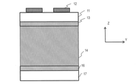
図1に、第1実施形態における、表示装置の構成例を模式的に示す。表示装置は、表示パネル5と、表示パネルの前側に配置された光線方向制御タッチパネル1とを含む。表示パネル5の種類は任意である。表示パネル5は、例えば、液晶表示パネル又はOLED(Organic Light Emitting Diode)表示パネルである。
<First Embodiment>
〔Constitution〕
FIG. 1 schematically shows a configuration example of a display device according to the first embodiment. The display device includes a
本開示において、表示パネル5の画像を視認するユーザの側つまり画像の光線が進む側を、表示装置の前側又は上側と呼び、その反対側を後側又は下側と呼ぶ。また、表示パネル5及び光線方向制御タッチパネル1の主面に垂直な方向をZ軸方向、主面内の垂直な2方向をそれぞれX軸方向(第2方向)及びY軸方向(第1方向)と呼ぶ。Z軸方向は、表示パネル5と光線方向制御タッチパネル1の積層方向である。
In the present disclosure, the side of the user who visually recognizes the image of the
光線方向制御タッチパネル1は、タッチパネルの機能を有すると共に、表示パネル5からの光線のうち通過する光線の方向を制御する機能を有する。光線方向制御タッチパネル1は、広視野状態と狭視野状態を切り替えて、表示パネル5の画像を透過させることができる。光線方向制御タッチパネル1からの出射方向の範囲が広い状態(モード)を広視野状態(広視野モード)と呼び、出射方向の範囲が狭い状態(モード)を狭視野状態(狭視野モード)と呼ぶ。
The light ray direction
図2に、光線方向制御タッチパネル1の断面構造例を模式的に示す。図2は、広視野状態の光線方向制御タッチパネル1を示す。光線方向制御タッチパネル1は、有色電気泳動粒子(有色荷電粒子)140の状態を変化させて、各光透過領域15及び分散剤141を透過する光の出射方向の範囲を変化させる。
FIG. 2 schematically shows an example of a cross-sectional structure of the light ray direction
光線方向制御タッチパネル1は、接着層3によって、表示パネル5の前面(上面)に接着されている。光線方向制御タッチパネル1と表示パネル5との間の接着層3は双方の周辺領域のみに設けられていてもよい。
The light ray direction
光線方向制御タッチパネル1は、上部透明基板11と下部透明基板17とを含む。下部透明基板17の下面は表示パネル5と対向し、上面は上部透明基板11の下面と対向する。上部透明基板11及び下部透明基板17は、それぞれ、例えば、ガラス、PET(Poly Ethylene Terephthalate)、PC(Poly Carbonate)製、又はPEN(Poly Ethylene Naphthalate)で形成されている。上部透明基板11及び下部透明基板17は、それぞれ、不撓性又は可撓性の絶縁体である。
The light ray direction
光線方向制御タッチパネル1は、さらに、複数の上部タッチパネル電極12、複数の下部タッチパネル電極13、及び複数の下部光線方向制御電極16を含む。上部タッチパネル電極12、下部タッチパネル電極13、下部光線方向制御電極16は、透明電極であり、例えば、ITO(Indium Tin Oxide)、ZnO、又はIGZOで形成されている。
The ray direction
複数の下部光線方向制御電極16(下部光線方向制御電極パターン)は、下部透明基板17の上面上に存在する。下部光線方向制御電極16は、それぞれ、下部透明基板17上でY軸方向において延在し、X軸方向に互いに離間して配列されている。各下部光線方向制御電極16は、例えば、1本の短冊状導体である。
The plurality of lower ray direction control electrodes 16 (lower ray direction control electrode patterns) exist on the upper surface of the lower
複数の下部タッチパネル電極13(下部タッチパネル電極パターン)は、上部透明基板11の下面上に存在する。下部光線方向制御電極16間又は下部タッチパネル電極13間のどちらか一方は、絶縁材料(後述するリブ15)で埋められている。下部タッチパネル電極13は、それぞれ、上部透明基板11上でY軸方向において延在し、X軸方向に互いに離間して配列されている。各下部タッチパネル電極13は、例えば、1本の短冊状導体である。下部タッチパネル電極13は、それぞれ、下部光線方向制御電極16と対向している。
The plurality of lower touch panel electrodes 13 (lower touch panel electrode patterns) exist on the lower surface of the upper
後述するように、下部タッチパネル電極13は、上部光線方向制御電極でもある。一例において、下部タッチパネル電極13は、対応する下部光線方向制御電極16と一対一で対向する。一例において、下部タッチパネル電極13は、それぞれ、対向する下部光線方向制御電極16と同様の形状を有する。複数の各下部光線方向制御電極16が、一つの下部タッチパネル電極13に対向してもよく、複数の下部タッチパネル電極13が、一つの下部光線方向制御電極16に対向してもよい。
As will be described later, the lower
複数の上部タッチパネル電極12(上部タッチパネル電極パターン)は、上部透明基板11の上面上に存在する。上部タッチパネル電極12は、窒化シリコンのような絶縁材料で覆われている。上部タッチパネル電極12は、それぞれ、上部透明基板11上でX軸方向において延在し、Y軸方向に互いに離間して配列されている。各上部タッチパネル電極12は、例えば、1本の短冊状導体である。
The plurality of upper touch panel electrodes 12 (upper touch panel electrode patterns) are present on the upper surface of the upper
光線方向制御タッチパネル1は、上部透明基板11と下部透明基板17との間の光線方向制御層を含む。光線方向制御層は、複数の電気泳動素子14及び複数のリブ15とで構成されている。リブ15は光透過領域である。電気泳動素子14及びリブ15は、それぞれ、Y軸方向において延在しており、X軸方向において交互に配列されている。
The light ray direction
XY面において、複数の電気泳動素子14は、Y軸方向に延在し、X軸方向に配列されたストライプパターンを有する。同様に、複数のリブ15は、Y軸方向に延在し、X軸方向に配列されたストライプパターンを有する。
On the XY plane, the plurality of
リブ15は、例えば光硬化性材料によって形成されている。リブ15の高さは、例えば、3μm~300μmであり、リブ15の幅は、例えば、1μm~150μmであり、リブ15のピッチは、例えば、0.25μm~40μmである。下部タッチパネル電極13の幅及びピッチは、それぞれ、例えば、数mmであり、上部タッチパネル電極12の幅及びピッチも、それぞれ、例えば、数mmである。図2の模式図において、二つの電気泳動素子14が一対の電極に挟まれているが、典型的な光線方向制御タッチパネル1においては、より多くの電気泳動素子14が一対の電極に挟まれている。
The
各電気泳動素子14は、リブ15の間に形成された空間内に収容されている電気泳動粒子140と分散剤141(電気泳動素子材料)を含む。電気泳動粒子140は有色であり、例えば、黒である。分散剤141は例えば無色透明な液体の材料で形成されている。
Each
各電気泳動素子14は、一つの下部タッチパネル電極13と一つの下部光線方向制御電極16とに挟まれている。図2の例において、下部タッチパネル電極13と下部光線方向制御電極16とは、電気泳動粒子140と分散剤141からなる電気泳動素子材料に接触している。下部タッチパネル電極13及び下部光線方向制御電極16の一方又は双方と電気泳動素子材料との間に絶縁層が存在してもよい。絶縁層は、例えば、酸化シリコン又は窒化シリコンである。
Each
図2の例において、連続する複数の電気泳動素子14(及び複数のリブ15)が一つの下部タッチパネル電極13と一つの下部光線方向制御電極16とに挟まれている。つまり、各下部タッチパネル電極13は、Z軸方向において複数の電気泳動素子14に対向している。同様に、各下部光線方向制御電極16は、Z軸方向において複数の電気泳動素子14に対向している。
In the example of FIG. 2, a plurality of continuous electrophoresis elements 14 (and a plurality of ribs 15) are sandwiched between one lower
他の例において、電気泳動素子14は、それぞれ、下部タッチパネル電極13と下部光線方向制御電極16の異なるペアに挟まれていてもよい(図13A参照)。複数の電気泳動素子14は、一つの下部タッチパネル電極13と複数の各下部光線方向制御電極16との間に挟まれていてもよい。複数の電気泳動素子14は、複数の下部タッチパネル電極13と一つの下部光線方向制御電極16との間に挟まれていてもよい。
In another example, the
図3に、狭視野状態の光線方向制御タッチパネル1を示す。狭視野状態において、各電気泳動素子14中の電気泳動粒子140は、分散剤141内に分散している。分散している電気泳動粒子140が表示パネル5からの光を吸収することで、電気泳動素子14は、表示パネル5からの光を遮蔽する。これにより、X軸方向において狭い出射角度範囲内の光線51のみが、光線方向制御タッチパネル1を通過する。
FIG. 3 shows a light ray direction
狭視野状態において、各電気泳動素子14を挟む下部タッチパネル電極13と下部光線方向制御電極16とは、同電位に維持される。これにより、電気泳動粒子140は、分散剤141内で分散した状態に維持される。下部タッチパネル電極13は、タッチパネル機能のために、特定の信号が与えられる。下部タッチパネル電極13及び下部光線方向制御電極16の電位制御の詳細は後述する。
In the narrow field of view, the lower
図4に、広視野状態の光線方向制御タッチパネル1を示す。広視野状態は、電気泳動粒子140を、電気泳動素子14を挟む電極の一方、例えば、下部光線方向制御電極16の近傍に凝集させることにより実現される。電気泳動素子14の大部分の領域は透明な分散剤141のみで構成され、電気泳動素子14は透過状態となる。これにより、X軸方向において広い出射角度範囲内の光線51が、光線方向制御タッチパネル1を通過する。
FIG. 4 shows a light ray direction
広視野状態において、下部タッチパネル電極13に対する下部光線方向制御電極16の相対電位は、電気泳動粒子140の電荷とは逆の極性を有する(電位差V)。これにより、電気泳動粒子140が下部光線方向制御電極16の近傍に集まる。
In the wide field of view, the relative potential of the lower ray
例えば、電気泳動粒子140の電荷が負(-)の場合には、下部光線方向制御電極16が正極となるように、下部光線方向制御電極16と下部タッチパネル電極13と所定電位が与えられる。電気泳動粒子140の電荷が正(+)の場合には、下部光線方向制御電極16が負極となるように、下部光線方向制御電極16と下部タッチパネル電極13とに所定電位が与えられる。電位差Vは、例えば20V~25V程度であればよい。
For example, when the charge of the
なお、以下の説明において、電気泳動粒子140の電荷は負であるとする。電気泳動粒子140の電荷が正の場合、下部光線方向制御電極16の極性を逆にすることにより、同様に対応可能である。
In the following description, it is assumed that the charge of the
〔制御〕
以下において、光線方向制御タッチパネル1の制御を説明する。上述のように、光線方向制御タッチパネル1は、タッチパネル機能と光線方向制御機能を有する。二つの機能を提供するため、光線方向制御タッチパネル1は、光線方向制御パネル部7と、光線方向制御パネル部7の前側のタッチパネル部8とで構成されている。
〔control〕
Hereinafter, the control of the light ray direction
タッチパネル部8は、上部タッチパネル電極12、上部透明基板11、及び下部タッチパネル電極13で構成されている。光線方向制御パネル部7は、上部透明基板11、下部タッチパネル電極13、電気泳動素子14、リブ15、下部光線方向制御電極16、及び下部透明基板17で構成されている。
The touch panel unit 8 is composed of an upper
上部透明基板11及び下部タッチパネル電極13は、タッチパネル部8と光線方向制御パネル部7とで共有されている。これにより、光線方向制御タッチパネル1の厚みを薄くすると共に、表示画像の視認性及びタッチパネルの操作性を高めることができる。
The upper
下部タッチパネル電極13には、タッチパネル機能を提供するための信号(電位)が与えられる。上述のように、下部タッチパネル電極13は、上部光線方向制御電極としてしても働く。したがって、下部タッチパネル電極13の電位に応じて、電気泳動粒子140の状態を適切に制御するための電位を下部光線方向制御電極16に与える必要がある。
A signal (potential) for providing the touch panel function is given to the lower
下部タッチパネル電極13を、タッチパネル部8と光線方向制御パネル部7で共有するため、本開示の光線方向制御タッチパネル1は、投影型静電容量方式を採用する。投影型静電容量方式のタッチパネルは、電極と指示体との間で発生する静電容量の変化を検出して、指示体の接触位置を検出する。
Since the lower
投射型容量方式のタッチパネルの容量検出方式として、自己容量検出方式と相互容量検出方式が存在する。自己容量検出方式のタッチパネルは、複数のX電極と複数のY電極を有する。X電極及びY電極は、マトリックス状に配置され、X電極及びY電極は、絶縁体を介して配置されている。 As the capacity detection method of the projection type touch panel, there are a self-capacity detection method and a mutual capacity detection method. The self-capacity detection type touch panel has a plurality of X electrodes and a plurality of Y electrodes. The X electrode and the Y electrode are arranged in a matrix, and the X electrode and the Y electrode are arranged via an insulator.
自己容量検出方式は、X電極、Y電極を独立に駆動して、それぞれの電極における静電容量値の変化を検出する。指示体が電極に近づくと、当該電極の静電容量が増加する。自己容量方式は、静電容量が増加したX電極及びY電極をそれぞれ検出することで、指示体の位置を検出する。 In the self-capacitance detection method, the X electrode and the Y electrode are independently driven to detect a change in the capacitance value in each electrode. As the indicator approaches the electrode, the capacitance of the electrode increases. The self-capacitance method detects the position of the indicator by detecting the X electrode and the Y electrode whose capacitance has increased, respectively.
相互容量方式のタッチパネルは、駆動電極としての送信電極(例えばX電極)と検出電極としての受信電極(例えばY電極)を有する。駆動電極及び検出電極は、マトリックス状に配置され、駆動電極及び検出電極は、絶縁体を介して配置されている。駆動電極及び検出電極の各交点に容量(交点容量)が構成される。交点容量の近傍に指示体が存在すると、交点における電界の一部が指示体に移動する。このため、交点容量が減少する。相互容量方式は、相互容量の変化がどの交点でどの程度の大きさで発生したかを検出することで、指示体の位置を検出する。 The mutual capacitance type touch panel has a transmission electrode (for example, an X electrode) as a drive electrode and a reception electrode (for example, a Y electrode) as a detection electrode. The drive electrode and the detection electrode are arranged in a matrix, and the drive electrode and the detection electrode are arranged via an insulator. A capacitance (intersection capacitance) is configured at each intersection of the drive electrode and the detection electrode. When the indicator is present in the vicinity of the intersection capacitance, a part of the electric field at the intersection moves to the indicator. Therefore, the intersection capacity is reduced. The mutual capacitance method detects the position of the indicator by detecting at which intersection and at what magnitude the change in mutual capacitance occurs.
以下に説明する光線方向制御タッチパネル1及びその制御例は、自己容量方式によるタッチ検出及び/又は相互容量方式によるタッチ検出を実行する。図5Aは、光線方向制御タッチパネル1の一部構成要素の関係を示す平面である。
The ray direction
複数の上部タッチパネル電極12が、Y軸方向に互いに離間して配列されている。上部タッチパネル電極12は、X軸方向に延びており、短冊状の形状を有する。上部タッチパネル電極12の形状は共通である。複数の下部タッチパネル電極13が、X方向に互いに離間して配列されている。下部タッチパネル電極13は、Y軸方向に延びており、短冊状の形状を有する。下部タッチパネル電極13の形状は共通である。
A plurality of upper
このように、上部タッチパネル電極12と下部タッチパネル電極13とは、マトリックス状に配置されている。また、図2を参照して説明したように、上部タッチパネル電極12と下部タッチパネル電極13は、絶縁体である上部透明基板11を挟むように、上部透明基板11の上面及び下面にそれぞれ配置されている。後述するように、上部タッチパネル電極12は相互容量方式の検出電極であり、下部タッチパネル電極13は送信電極である。
As described above, the upper
複数の電気泳動素子14が、X方向に互いに離間して配列されている。電気泳動素子14は、Y軸方向に延びており、直方体形状を有する。電気泳動素子14の形状は共通である。図5Aにおいて不図示の下部光線方向制御電極16は、下部透明基板17の上面において、下部タッチパネル電極13と同様にレイアウトされている。複数の電気泳動素子14と対向する下部光線方向制御電極16のパターンと、複数の電気泳動素子14と対向する下部タッチパネル電極13のパターンとは、一致している。
A plurality of
図5Bに、図5AのBB切断線における光線方向制御タッチパネル1の断面構造を模式的に示す。BB切断線は、X軸方向に平行な線であり、図5Bは、Y軸方向において見た断面構造である。図5Bに示す断面構造は、図2、3、及び4を参照して説明した構造と同様である。
FIG. 5B schematically shows the cross-sectional structure of the light ray direction
図5Bに示す例において、各下部タッチパネル電極13は、複数の電気泳動素子14に対向し、同様に、各下部光線方向制御電極16は、複数の電気泳動素子14に対向する。つまり、下部タッチパネル電極13と下部光線方向制御電極16の各ペアは、複数の電気泳動素子14を挟み、これら複数の電気泳動素子14を駆動する。図5Bの例においては、各下部タッチパネル電極13は一つのみの下部光線方向制御電極16に対向する。対向する下部タッチパネル電極13と下部光線方向制御電極16は、同一の電気泳動素子14を駆動する。
In the example shown in FIG. 5B, each lower
図5Cに、図5AのCC切断線における光線方向制御タッチパネル1の断面構造を模式的に示す。CC切断線は、Y軸方向に平行な線であり、図5Cは、X軸方向において見た断面構造である。図5Cは、電気泳動素子14における光線方向制御タッチパネル1の断面構造である。各電気泳動素子14の全上面は、一つの下部タッチパネル電極13と対向し、その全下面は一つの下部光線方向制御電極16と対向している。
FIG. 5C schematically shows the cross-sectional structure of the light ray direction
図6に、表示装置の制御系の論理構成を模式的に示す。表示装置は、タッチパネル制御部21、光線方向制御部23、タイミング制御部24、及びメイン制御部25を含む。これらは、それぞれ、プログラムに従って動作するプロセッサ及び/又は特定機能の論理回路を含んで構成される。タッチパネル制御部21、光線方向制御部23、タイミング制御部24、及びメイン制御部25は、それぞれ個別の回路で構成されてもおく、これらの一部又は全部は同一の回路(プロセッサを含む)を共有してもよい。
FIG. 6 schematically shows the logical configuration of the control system of the display device. The display device includes a touch panel control unit 21, a ray
タッチパネル制御部21は、光線方向制御タッチパネル1のタッチパネル部8を制御し、光線方向制御タッチパネル1のタッチパネル機能を実現する。具体的には、タッチパネル制御部21は、タイミング制御部24からのタイミング信号に応じて、上部タッチパネル電極12及び下部タッチパネル電極13を制御する。
The touch panel control unit 21 controls the touch panel unit 8 of the ray direction
本例において、タッチパネル制御部21は、自己容量方式及び相互容量方式のいずれの方式でも指示体のタッチ位置を検出できる。タッチパネル制御部21は、メイン制御部25からの指示に応じて、タッチ位置検出のモードを切り替える。他の例において、タッチパネル制御部21は、自己容量方式及び相互容量方式の一方のみでタッチ検出可能でもよい。
In this example, the touch panel control unit 21 can detect the touch position of the indicator by either the self-capacity method or the mutual capacity method. The touch panel control unit 21 switches the touch position detection mode in response to an instruction from the
タッチパネル制御部21は、タイミング制御部24からのタイミング信号に応じて、上部タッチパネル電極12及び下部タッチパネル電極13における駆動電極を駆動し、さらに、検出電極における容量変化を検出する。相互容量方式においては、送信電極が駆動電極であり、受信電極が検出電極である。本例において、上部タッチパネル電極12が検出電極であり、下部タッチパネル電極13が駆動電極である。自己容量方式においては、各電極が駆動電極であると共に、検出電極でもある。
The touch panel control unit 21 drives the drive electrodes in the upper
光線方向制御部23は、光線方向制御タッチパネル1の光線方向制御パネル部7を制御し、光線方向制御タッチパネル1の光線方向制御(視野角制御)機能を実現する。具体的には、光線方向制御部23は、タイミング信号に応じて、下部光線方向制御電極16を制御する。後述するように、光線方向制御部23は、下部タッチパネル電極13の駆動電位に応じて下部光線方向制御電極16を駆動することで、光線方向制御タッチパネル1の狭視野角モード及び広視野角モードそれぞれにおいて、通過する表示パネル5からの光の方向(視野角)を適切に制御する。
The ray
メイン制御部25は、表示パネル5、タッチパネル制御部21、及び光線方向制御部23を制御する。メイン制御部25は、表示パネル5を制御して画像を表示させる。表示パネル5は、メイン制御部25からの信号に従って、画素を制御して画像を表示する。メイン制御部25は、タッチパネル制御部21から指示体の位置を示す情報を取得すると共に、タッチパネル制御部21によるタッチ検出のモード(自己容量モード/相互容量モード)を制御する。
The
図7に、光線方向制御部23の一部の論理構成例を模式的に示す。図7は構成例を示しており、同様の機能を実装できれば光線方向制御部23どのような構成を有してもよい。図7は、一つの下部光線方向制御電極16を駆動するための構成例を示している。光線方向制御部23は、スイッチ231及びスイッチ制御部232を含む。スイッチ231は、対応する下部光線方向制御電極16に接続され、当該下部光線方向制御電極16を駆動するための信号(電位)を出力する。
FIG. 7 schematically shows an example of a logical configuration of a part of the ray
光線方向制御部23は、下部光線方向制御電極16それぞれを駆動するスイッチ231を含む。スイッチ制御部232は、メイン制御部25からの視野角モードの指定に応じて、スイッチ231を制御する。
The ray
各下部光線方向制御電極16に対応する下部タッチパネル電極13に対する駆動電位V1と同電位の信号が、光線方向制御部23内で生成される。スイッチ231は、駆動電位V1及び駆動電位V1に定電圧が加えられた電位(のライン/端子)の一方を選択する。具体的には、スイッチ231は、狭視野角モードにおいて駆動電位V1を選択し、広視野角モードにおいて駆動電位V1に定電圧が加えられた電位を選択する。スイッチ231が、視野角モードに応じて同様に制御される。
A signal having the same potential as the drive potential V1 for the lower
〔相互容量方式及び狭視野角モード〕
図8A、8B及び8Cに、相互容量方式によるタッチ検出及び狭視野角モードでの、電極の駆動方法の例を示す。タッチパネル制御部21は、下部タッチパネル電極13を順次選択する。タッチパネル制御部21は、選択している下部タッチパネル電極13に駆動電位を与えながら、上部タッチパネル電極12それぞれにおいて容量を測定する。タッチパネル制御部21は、上部タッチパネル電極12を順次選択して容量を測定してもよく、全ての上部タッチパネル電極12と選択している下部タッチパネル電極13との間の容量を同時に測定してもよい。
[Mutual capacitance method and narrow viewing angle mode]
8A, 8B and 8C show an example of a method of driving an electrode in a touch detection by a mutual capacitance method and a narrow viewing angle mode. The touch panel control unit 21 sequentially selects the lower
図8Aに示す例において、タッチパネル制御部21は、下部タッチパネル電極13A、13B、及び13Cの順で、下部タッチパネル電極を選択する。図8Aにおいて、下部タッチパネル電極13Bが選択されており、下部タッチパネル電極13Bに駆動電位が与えられている。
In the example shown in FIG. 8A, the touch panel control unit 21 selects the lower touch panel electrodes in the order of the lower
図8Bは、容量測定のために選択されている下部タッチパネル電極13B及び対向する下部光線方向制御電極16Bに与えられる駆動電位(駆動信号)の波形31である。同一波形31の信号が、対向する下部タッチパネル電極13Bと下部光線方向制御電極16Bとに与えられる。
FIG. 8B is a
図8Cは、下部タッチパネル電極13A及び13C、並びに、下部光線方向制御電極16A及び16Cに与えられている電位(信号)の波形32である。同一の波形32の信号が、下部タッチパネル電極13A及び13C、並びに、下部光線方向制御電極16A及び16Cに与えられる。
FIG. 8C is a
図8Bに示すように、容量測定のために選択された下部タッチパネル電極13Bに対して、交流信号が与えられる。図8Bに示す例において、下部タッチパネル電極13Bに与えられる信号は矩形波である。容量測定のための駆動電位波形は任意であって、光線方向制御タッチパネル1によるタッチ検出のために適切な波形が選択される。
As shown in FIG. 8B, an AC signal is given to the lower
図8Bに示し、図7を参照して説明したように、狭視野角モードにおいて下部光線方向制御電極16Bに対して与えられる駆動電位は、対向する下部タッチパネル電極13Bに対して与えられる駆動電位と同一である。下部光線方向制御電極16Bと下部タッチパネル電極13Bの間に挟まれている電気泳動素子14それぞれの両端は同電位であり、有色電気泳動粒子140は、分散剤141内で略均等に分散した状態にある。
As shown in FIG. 8B and described with reference to FIG. 7, the drive potential given to the lower ray
図8Cに示し、図7を参照して説明したように、容量測定のために選択されている下部タッチパネル電極13B以外の下部タッチパネル電極13A、13Cには、一定の基準電位(例えば接地電位)が与えられる。下部タッチパネル電極13A、13Cそれぞれに対向する、下部光線方向制御電極16A、16Cに対しても、同様に、一定の基準電位が与えられる。
As shown in FIG. 8C and described with reference to FIG. 7, the lower
下部光線方向制御電極16Aと下部タッチパネル電極13Aの間に挟まれている電気泳動素子14の両端は同電位であり、また、下部光線方向制御電極16Cと下部タッチパネル電極13Cの間に挟まれている電気泳動素子14の両端は同電位である。つまり、全ての下部光線方向制御電極16と全ての下部タッチパネル電極13の間に挟まれている電気泳動素子14それぞれの両端は同電位である。全ての電気泳動素子14それぞれの両端は同電位であり、有色電気泳動粒子140は、分散剤141内で略均等に分散した状態にある。
Both ends of the
上述のように、光線方向制御部23は、相互容量方式のタッチ検出及び狭視野モードにおいて、各電気泳動素子14の下部光線方向制御電極16に対して、対向する下部タッチパネル電極13と同一の電位(信号)を与える。これにより、各電気泳動素子14内の有色電気泳動粒子140は、分散剤141内で略均等に分散した状態に維持される。
As described above, the ray
〔相互容量方式及び広視野角モード〕
図9A、9B及び9Cに、相互容量方式によるタッチ検出及び広視野角モードでの、電極の駆動方法の例を示す。広視野状態は、電気泳動粒子140を、電気泳動素子14を挟む電極の一方、本例において、下部光線方向制御電極16の近傍に凝集させることにより実現される。電気泳動粒子140は、下部タッチパネル電極13の近傍に凝集させてもよい。
[Mutual capacitance method and wide viewing angle mode]
9A, 9B and 9C show an example of a method of driving an electrode in a touch detection by a mutual capacitance method and a wide viewing angle mode. The wide field of view state is realized by aggregating the
図9Aに示す例において、タッチパネル制御部21は、下部タッチパネル電極13A、13B、及び13Cの順で、下部タッチパネル電極を選択する。図9Aにおいて、下部タッチパネル電極13Bが選択されており、下部タッチパネル電極13Bに駆動電位が与えられている。
In the example shown in FIG. 9A, the touch panel control unit 21 selects the lower touch panel electrodes in the order of the lower
図9Bは、容量測定のために選択されている下部タッチパネル電極13Bに与えられる駆動電位(駆動信号)の波形34、及び、対向する下部光線方向制御電極16Bに与えられる駆動電位(駆動信号)の波形33である。これらの駆動電位の間には、所定の電位差Vが存在する。
FIG. 9B shows the
図9Cは、下部タッチパネル電極13A及び13Cに与えられている電位(信号)の波形36、並びに、下部光線方向制御電極16A及び16Cに与えられている電位(信号)の波形35である。これら電位の間には、所定の電位差Vが存在する。
FIG. 9C is a
図9Bに示すように、容量測定のために選択された下部タッチパネル電極13Bに対して、交流信号が与えられる。図9Bに示す例において、下部タッチパネル電極13Bに与えられる信号は矩形波である。
As shown in FIG. 9B, an AC signal is given to the lower
図9Bに示し、図7を参照して説明したように、広視野角モードにおいて下部光線方向制御電極16Bに対して与えられる駆動電位は、下部タッチパネル電極13Bに与えられる駆動電位に一定電圧(一定電位差)Vを加えた電位である。
As shown in FIG. 9B and described with reference to FIG. 7, the drive potential given to the lower ray
下部光線方向制御電極16Bと下部タッチパネル電極13Bの間に挟まれている電気泳動素子14それぞれの両端は電圧Vが加えられ、下部光線方向制御電極16Bの極性は、下部タッチパネル電極13Bに対して正である。したがって、負に帯電している有色電気泳動粒子140は、下部光線方向制御電極16Bの近傍に凝集する。
A voltage V is applied to both ends of each of the
図9Cに示し、図7を参照して説明したように、容量測定のために選択されている下部タッチパネル電極13B以外の下部タッチパネル電極13A、13Cには、一定の基準電位(例えば接地電位)が与えられる。下部タッチパネル電極13A、13Cそれぞれに対向する、下部光線方向制御電極16A、16Cに対して、下部タッチパネル電極13A、13Cに与えられる電位に一定電圧Vを加えた電位が与えられる。
As shown in FIG. 9C and described with reference to FIG. 7, the lower
下部光線方向制御電極16Aと下部タッチパネル電極13Aの間に挟まれている電気泳動素子14には電圧Vが与えられ、下部光線方向制御電極16Aの相対極性が正である。また、下部光線方向制御電極16Cと下部タッチパネル電極13Cの間に挟まれている電気泳動素子14には電圧Vが与えられ、下部光線方向制御電極16Cの相対極性が正である。
A voltage V is applied to the
つまり、全ての下部光線方向制御電極16と全ての下部タッチパネル電極13の間に挟まれている電気泳動素子14それぞれの両端の電位差はVであり、下部光線方向制御電極16の相対極性が正である。有色電気泳動粒子140は、下部光線方向制御電極16近傍に凝集した状態にある。
That is, the potential difference between both ends of each of the
上述のように、光線方向制御部23は、相互容量方式のタッチ検出及び広視野モードにおいて、各電気泳動素子14の下部光線方向制御電極16に対して、対向する下部タッチパネル電極13への電位(信号)に一定電圧を加えた電位を与える。これにより、各電気泳動素子14内の有色電気泳動粒子140は、下部光線方向制御電極16近傍に凝集した状態に維持される。
As described above, the light ray
〔自己容量方式及び狭視野角モード〕
図10A及び10Bに、自己容量方式によるタッチ検出及び狭視野角モードでの、電極の駆動方法の例を示す。タッチパネル制御部21は、全ての上部タッチパネル電極12及び全ての下部タッチパネル電極13に駆動電位を与えつつ、全ての上部タッチパネル電極12及び全ての下部タッチパネル電極13の容量を測定する。これと異なり、タッチパネル制御部21は、上部タッチパネル電極12及び下部タッチパネル電極13を順次選択し、選択している電極に駆動信号を与えると共に、その容量を測定してもよい。
[Self-capacity method and narrow viewing angle mode]
FIGS. 10A and 10B show an example of an electrode driving method in the touch detection by the self-capacity method and the narrow viewing angle mode. The touch panel control unit 21 measures the capacities of all the upper
図10Aに示す例において、タッチパネル制御部21は、全ての下部タッチパネル電極13A、13B、及び13Cに同時に駆動電位を与える。図10Bは、下部タッチパネル電極13A、13B及び13C、並びに、下部光線方向制御電極16A、16B及び16Cに与えられている電位(信号)の波形41である。
In the example shown in FIG. 10A, the touch panel control unit 21 applies a drive potential to all the lower
同一の波形41の駆動信号が、下部タッチパネル電極13A、13B及び13C、並びに、下部光線方向制御電極16A、16B及び16Cに与えられる。なお、容量測定のための駆動波形は任意であって、光線方向制御タッチパネル1によるタッチ検出のために適切な波形が選択される。
Drive signals having the
図10Bに示し、図7を参照して説明したように、狭視野角モードにおいて下部光線方向制御電極16A、16B及び16Cに対して与えられる駆動電位は、対向する下部タッチパネル電極13A、13B、13Cに対して与えられる駆動電位と同一である。
As shown in FIG. 10B and described with reference to FIG. 7, the drive potential applied to the lower ray
本例において、全ての下部光線方向制御電極16と全ての下部タッチパネル電極13の間に挟まれている電気泳動素子14それぞれの両端は同電位である。全ての電気泳動素子14それぞれの両端は同電位であり、有色電気泳動粒子140は、分散剤141内で略均等に分散した状態(分散状態)にある。
In this example, both ends of each of the
上述のように、光線方向制御部23は、自己容量方式のタッチ検出及び狭視野モードにおいて、各電気泳動素子14の下部光線方向制御電極16に対して、対向する下部タッチパネル電極13と同一の電位(信号)を与える。これにより、各電気泳動素子14内の有色電気泳動粒子140は、分散剤141内で略均等に分散した状態に維持される。
As described above, the ray
〔自己容量方式及び広視野角モード〕
図11A及び11Bに、自己容量方式によるタッチ検出及び広視野角モードでの、電極の駆動方法の例を示す。広視野状態は、電気泳動粒子140を、電気泳動素子14を挟む電極の一方、本例において、下部光線方向制御電極16の近傍に凝集させることにより実現される。
[Self-capacity method and wide viewing angle mode]
FIGS. 11A and 11B show an example of a method of driving the electrodes in the touch detection by the self-capacity method and the wide viewing angle mode. The wide field of view state is realized by aggregating the
図11Aに示す例において、タッチパネル制御部21は、全ての下部タッチパネル電極13A、13B、及び13Cに同時に駆動電位を与える。図11Bは、容量測定のために全ての下部タッチパネル電極13A、13B及び13Cに与えられる駆動電位(駆動信号)の波形43、及び、対向する下部光線方向制御電極16A、16B及び16Cに与えられる駆動電位(駆動信号)の波形42を示す。これらの駆動電位の間には、所定の電位差Vが存在する。
In the example shown in FIG. 11A, the touch panel control unit 21 applies a drive potential to all the lower
図11Bに示すように、容量測定のために全下部タッチパネル電極13A、13B、13Cに対して、交流信号が与えられる。図11Bに示す例において、下部タッチパネル電極13A、13B及び13Cに与えられる信号は矩形波である。
As shown in FIG. 11B, an AC signal is given to all the lower
図11Bに示し、図7を参照して説明したように、広視野角モードにおいて下部光線方向制御電極16A、16B及び16Cに対して与えられる駆動電位は、下部タッチパネル電極13A、13B及び13Cに与えられる駆動電位に一定電圧Vを加えた電位である。
As shown in FIG. 11B and described with reference to FIG. 7, the drive potential applied to the lower ray
下部光線方向制御電極16Aと下部タッチパネル電極13Aの間に挟まれている電気泳動素子14には電圧Vが与えられ、下部光線方向制御電極16Aの相対極性が正である。下部光線方向制御電極16Bと下部タッチパネル電極13Bの間に挟まれている電気泳動素子14には電圧Vが与えられ、下部光線方向制御電極16Bの相対極性が正である。下部光線方向制御電極16Cと下部タッチパネル電極13Cの間に挟まれている電気泳動素子14には電圧Vが与えられ、下部光線方向制御電極16Cの相対極性が正である。
A voltage V is applied to the
つまり、全ての下部光線方向制御電極16と全ての下部タッチパネル電極13の間に挟まれている電気泳動素子14それぞれの両端の電位差はVであり、下部光線方向制御電極16の相対極性が正である。有色電気泳動粒子140は、下部光線方向制御電極16近傍に凝集した状態(凝集状態)にある。
That is, the potential difference between both ends of each of the
上述のように、光線方向制御部23は、自己容量方式のタッチ検出及び広視野モードにおいて、各電気泳動素子14の下部光線方向制御電極16に対して、対向する下部タッチパネル電極13への電位(信号)に一定電圧を加えた電位を与える。これにより、各電気泳動素子14内の有色電気泳動粒子140は、下部光線方向制御電極16近傍に凝集した状態に維持される。
As described above, the light ray
図8A~図11Bを参照して説明した構成例において、各下部タッチパネル電極13は、一つのみの下部光線方向制御電極16に対向し、各下部光線方向制御電極16は、一つのみの下部タッチパネル電極13に対向する。光線方向制御タッチパネル1は、これと異なる構成を有してもよい。
In the configuration example described with reference to FIGS. 8A to 11B, each lower
上述のように、相互容量方式のタッチ検出及び自己容量方式のタッチ検出の双方において、光線方向制御部23は、狭視野角モードにおいて、各下部光線方向制御電極16に、対向する下部タッチパネル電極13と同電位が与える。相互容量方式のタッチ検出及び自己容量方式のタッチ検出の双方において、光線方向制御部23は、広視野角モードにおいて、各下部光線方向制御電極16には、対向する下部タッチパネル電極13の電位に一定電圧を加えた電位を与える。
As described above, in both the mutual capacitance type touch detection and the self-capacity method touch detection, the light ray
各下部タッチパネル電極13及び各下部光線方向制御電極16は、上記動作を可能とする様々な形状を有することができる。例えば、図8A~図9Cを参照して説明したように、駆動される下部タッチパネル電極13が順次選択される構成において、各下部光線方向制御電極16が、一つのみの下部タッチパネル電極13と対向し、各下部タッチパネル電極13は、複数の下部光線方向制御電極16と対向してもよい。
Each lower
各下部光線方向制御電極16に対向する全ての電気泳動素子14は、一つのみの下部タッチパネル電極13と対向する。連続する複数の電気泳動素子14は、一つの下部タッチパネル電極13と複数の下部光線方向制御電極16との間に挟まれ、それらに駆動される。
All the
図10A~図11Bを参照して説明したように、全ての下部タッチパネル電極13が同時に駆動される構成において、下部光線方向制御電極16の数及び形状は任意である。各下部光線方向制御電極16が対向する下部タッチパネル電極13の数は任意であり、各下部タッチパネル電極13が対向する下部光線方向制御電極16の数は任意である。例えば、下部光線方向制御電極16はべたパターンであり、全ての電気泳動素子14が、一つの下部光線方向制御電極16と複数の下部タッチパネル電極13に挟まれていてもよい。
As described with reference to FIGS. 10A to 11B, the number and shape of the lower ray
他の構成例において、上部タッチパネル電極12は、上部透明基板11の下面に形成されていてもよい。例えば、上部タッチパネル電極12は、上部透明基板11の下面と下部タッチパネル電極13と間に形成され、上部タッチパネル電極12と下部タッチパネル電極13との間には絶縁層、例えば、酸化シリコン又は窒化シリコン層が形成される。
In another configuration example, the upper
<他の実施形態>
以下において、光線方向制御タッチパネル1の他の構成を説明する。以下に説明する構成において、上部タッチパネル電極12及び下部タッチパネル電極13は、それぞれ、複数の電極片を連結した構成を有する。
<Other embodiments>
Hereinafter, another configuration of the light ray direction
図12Aに、上部タッチパネル電極12と下部タッチパネル電極13の上部透明基板11上でのパターンを、図12Bに、下部タッチパネル電極13の上部透明基板11上でのパターンを、図12Cに、上部タッチパネル電極12の上部透明基板11上でのパターンをそれぞれ示す。
12A shows the pattern of the upper
図12Bに示すように、下部タッチパネル電極13は、ダイヤモンドパターンを有する。具体的には、各下部タッチパネル電極13は、Y軸方向に配列された複数の菱型の電極片31と、それら菱型の電極片31の角を連結する連結部32とで構成されている。
As shown in FIG. 12B, the lower
下部タッチパネル電極13は、X軸方向に千鳥状に配列されている。各下部タッチパネル電極13の隣接する電極片31の間に、隣接下部タッチパネル電極13の電極片31が配置されている。全下部タッチパネル電極13の電極片31は、上部透明基板11の下面上で、千鳥状に配列されている。
The lower
図12Cに示すように、上部タッチパネル電極12は、ダイヤモンドパターンを有する。具体的には、各上部タッチパネル電極12は、X軸方向に配列された複数の菱型の電極片26と、それら菱型の電極片26の角を連結する連結部27とで構成されている。
As shown in FIG. 12C, the upper
上部タッチパネル電極12は、Y軸方向に配列されている。全上部タッチパネル電極12の電極片26のX軸方向における位置は、共通である。全上部タッチパネル電極12の電極片26は、上部透明基板11の上面上で、マトリックス状に配列されている。隣接する上部タッチパネル電極12の間には、電極片26に相当する空間123が存在する。
The upper
図12Aに示すように、全上部タッチパネル電極12の電極片26は、それぞれ、Z軸方向において、下部タッチパネル電極13の電極片31と(略完全に)重なる。下部タッチパネル電極13の一部の電極片31は、それぞれ、Z軸方向において見た場合に、上部タッチパネル電極12の間の空間123内に位置し、上部タッチパネル電極12の電極片26と部分的にも重なっていない。
As shown in FIG. 12A, the
全下部タッチパネル電極13の電極片31は、上部透明基板11上で、全上部タッチパネル電極12の電極片26よりも多くの面積を覆う。下部タッチパネル電極13の電極片31は、電気泳動素子14のより多くの面積を覆うように、配列されている。
The
図13Aに、電気泳動素子14、及び、上部タッチパネル電極12と下部タッチパネル電極13の上部透明基板11上でのパターンを示す。また図13Bに、図13AのBB切断線における、光線方向制御タッチパネル1の断面構成を、図13Cに、図13AのCC切断線における、光線方向制御タッチパネル1の断面構成を、図13Dに、図13AのDD切断線における、光線方向制御タッチパネル1の断面構成をそれぞれ示す。図13Eは、図13AのEE切断線における、光線方向制御タッチパネル1の断面構成を示す。
FIG. 13A shows the pattern of the
図13B~13Eに示すように、下部光線方向制御電極16は、下部透明基板17上に形成されたべたパターン、つまり、1枚の連続する透明電極である。タッチパネル制御部21は、図10A~11Bを参照して説明したように、自己容量方式よるタッチ検出を行う。
As shown in FIGS. 13B to 13E, the lower ray
本例において、タッチパネル制御部21は、全ての上部タッチパネル電極12及び全ての下部タッチパネル電極13に同時に同一波形の駆動電位を与え、容量を測定する。タッチパネル制御部21は、上部タッチパネル電極12の電極片と重なる電極片を有する下部タッチパネル電極13の容量を、測定しても測定しなくともよい。
In this example, the touch panel control unit 21 applies a drive potential of the same waveform to all the upper
光線方向制御部23は、全ての上部タッチパネル電極12及び全ての下部タッチパネル電極13への駆動電位に応じて、下部光線方向制御電極16を駆動する。第1実施形態で説明したように、光線方向制御部23は、狭視野角モードにおいて、タッチパネル電極と同電位を下部光線方向制御電極16に与える。光線方向制御部23は、広視野角モードにおいて、タッチパネル電極に一定電圧を加えた電位を下部光線方向制御電極16に与える。
The ray
他の構成例は、複数の下部光線方向制御電極16を含み、自己容量方式又は相互容量方式において、下部タッチパネル電極13を順次選択して駆動してもよい。図13Eの例において、電気泳動素子14は、二つの下部タッチパネル電極13A、13B(の電極片)と対向する。このように、一部の電気泳動素子14は、それぞれ、二つの下部タッチパネル電極13(の電極片)と対向する。
Another configuration example includes a plurality of lower ray
一例において、電気泳動素子14を挟む領域において下部タッチパネル電極13のパターンと一致するパターンを有する、下部光線方向制御電極16が形成されていてもよい。光線方向制御部23は、図8A~11Bを参照して説明したように、下部光線方向制御電極16を対向する下部タッチパネル電極13の電位に応じて駆動する。狭視野角モードにおいて、光線方向制御部23は、下部光線方向制御電極16に対して、対向する下部タッチパネル電極13と同電位を与える。広視野角モードにおいて、光線方向制御部23は、下部光線方向制御電極16に対して、対向する下部タッチパネル電極13の電位の一定電圧を加えた電位を与える。
In one example, the lower ray
タッチパネル制御部21は、上部タッチパネル電極12の電極片と重なる電極片を有する下部タッチパネル電極13に容量検出のための駆動電位を与えてもよく、与えなくてもよい。つまり、タッチパネル制御部21は、全下部タッチパネル電極13を順次選択してもよく、Z軸方向において見た場合に上部タッチパネル電極12間で露出している(上部タッチパネル電極12と重ならない)電極片を有する下部タッチパネル電極13のみを順次選択してもよい。
The touch panel control unit 21 may or may not give a drive potential for capacitance detection to the lower
図14A及び14Bに、光線方向制御タッチパネル1の他の構成例を示す。図14Aは、下部タッチパネル電極13と下部光線方向制御電極16との関係を示す平面図である。図14Aにおいて、下部タッチパネル電極13の電極片を連結する部分は省略されている。下部タッチパネル電極13のパターンは、図12Bに示すパターンと同様である。図14Bは、図14AのBB切断線における光線方向制御タッチパネル1の断面構造を模式的に示した図である。
14A and 14B show other configuration examples of the light ray direction
下部光線方向制御電極16は、下部透明基板17の上面において、電気泳動素子14が対向する領域内のみに形成される。これにより透過率が向上する。具体的には、下部透明基板17の上面に、Y軸方向の延び、X軸方向に離間して配列された、複数の下部光線方向制御電極ライン163が形成されている。図14Aは、一つの下部光線方向制御電極ラインが、例として、符号163で指示されている。
The lower ray
Z軸方向において見て、各下部光線方向制御電極ライン163は、一つの電気泳動素子14の下面と重なるように形成される。各下部光線方向制御電極ライン163は、1又は複数の下部光線方向制御電極16で構成されている。一つの下部光線方向制御電極ライン163は、1又は二つの下部タッチパネル電極13と対向する。各下部光線方向制御電極16は、一つの下部タッチパネル電極13とのみ対向する。
When viewed in the Z-axis direction, each lower ray direction
光線方向制御部23は、図8A~11Bを参照して説明したように、各下部光線方向制御電極16を対向する下部タッチパネル電極13の電位に応じて駆動する。狭視野角モードにおいて、光線方向制御部23は、下部光線方向制御電極16に対して、対向する下部タッチパネル電極13と同電位を与える。広視野角モードにおいて、光線方向制御部23は、下部光線方向制御電極16に対して、対向する下部タッチパネル電極13の電位の一定電圧を加えた電位を与える。
As described with reference to FIGS. 8A to 11B, the light ray
上記構成及び制御により、一つの電気泳動素子14が隣接する二つの下部タッチパネル電極13と対向する場合でも、その電気泳動素子14全体の電気泳動粒子140を視野角モードに応じた適切な状態に維持することができる。
With the above configuration and control, even when one
なお、下部透明基板17上には、下部光線方向制御電極16に駆動電位を与えるための配線が、下部光線方向制御電極16と同一材料で形成される。配線は、下部光線方向制御電極16と同一の層又は異なる層に形成される。
On the lower
図15に、光線方向制御タッチパネル1の他の構成例を示す。光線方向制御タッチパネル1は、視認するユーザに向かって凸の曲面形状を有する。本例において、光線方向制御タッチパネル1は、X軸沿った曲面を有する。つまり、面上でX軸方向の延びる線は曲線であり、Y軸方向の延びる線は直線である。この形状により、表示面周辺部の透過率を向上することができる。上部タッチパネル電極12、下部タッチパネル電極13、及び下部光線方向制御電極16は、上記の実施形態のいずれのパターンを有してもよい。
FIG. 15 shows another configuration example of the light ray direction
光線方向制御タッチパネル1の他の構成例において、タッチパネル電極は、上部透明基板11の上面に形成されておらず、上部透明基板11の下面のみに形成されていてもよい。例えば、X軸方向に延びY軸方向に配列された電極と、Y軸方向に延びX軸方向に配列された電極とが、絶縁層を介して、上部透明基板11の下面に形成される。タッチパネル制御部21は、自己容量方式によりタッチ位置を検出する。
In another configuration example of the light ray direction
以上、本発明の実施形態を説明したが、本発明が上記の実施形態に限定されるものではない。当業者であれば、上記の実施形態の各要素を、本発明の範囲において容易に変更、追加、変換することが可能である。ある実施形態の構成の一部を他の実施形態の構成に置き換えることが可能であり、ある実施形態の構成に他の実施形態の構成を加えることも可能である。 Although the embodiment of the present invention has been described above, the present invention is not limited to the above embodiment. A person skilled in the art can easily change, add, or convert each element of the above embodiment within the scope of the present invention. It is possible to replace a part of the configuration of one embodiment with the configuration of another embodiment, and it is also possible to add the configuration of another embodiment to the configuration of one embodiment.
1 光線方向制御タッチパネル、3 接着層、5 表示パネル、7 光線方向制御パネル部、8 タッチパネル部、11 上部透明基板、12 上部タッチパネル電極、13、13A、13B、13C 下部タッチパネル電極、14 電気泳動素子、15 リブ(光透過領域)、16、16A、16B、16C 下部光線方向制御電極、17 下部透明基板、21 タッチパネル制御部、23 光線方向制御部、24 タイミング制御部、25 メイン制御部、51 光線、123 空間、140 電気泳動粒子、141 分散剤、163 下部光線方向制御電極ライン、231 スイッチ
232 スイッチ制御部
1 ray direction control touch panel, 3 adhesive layer, 5 display panel, 7 ray direction control panel section, 8 touch panel section, 11 upper transparent substrate, 12 upper touch panel electrode, 13, 13A, 13B, 13C lower touch panel electrode, 14 electrophoretic element , 15 ribs (light transmission region), 16, 16A, 16B, 16C lower ray direction control electrode, 17 lower transparent substrate, 21 touch panel control unit, 23 ray direction control unit, 24 timing control unit, 25 main control unit, 51 ray , 123 space, 140 electrophoretic particles, 141 dispersant, 163 lower ray direction control electrode line, 231
Claims (13)
下部透明基板と、
前記下部透明基板の上面の1以上の下部光線方向制御電極と、
前記上部透明基板の下面の複数のタッチパネル電極と、
前記1以上の下部光線方向制御電極と前記複数のタッチパネル電極とに挟まれ、それぞれが有色電気泳動粒子と分散材とを含む、複数の電気泳動素子と、
制御部と、を含み、
前記制御部は、
前記複数のタッチパネル電極に、タッチ位置検出のための容量測定において駆動電位を供給し、
前記複数のタッチパネル電極に与える駆動電位に応じて前記1以上の下部光線方向制御電極に対して駆動電位を供給し、前記複数の電気泳動素子における前記有色電気泳動粒子の状態を制御する、
光線方向制御タッチパネル装置。 With the upper transparent board,
With the lower transparent board,
One or more lower ray direction control electrodes on the upper surface of the lower transparent substrate,
A plurality of touch panel electrodes on the lower surface of the upper transparent substrate,
A plurality of electrophoresis elements sandwiched between the one or more lower ray direction control electrodes and the plurality of touch panel electrodes, each containing colored electrophoresis particles and a dispersant.
Including the control unit
The control unit
A drive potential is supplied to the plurality of touch panel electrodes in capacity measurement for touch position detection.
A driving potential is supplied to the one or more lower ray direction control electrodes according to the driving potential applied to the plurality of touch panel electrodes, and the state of the colored electrophoresis particles in the plurality of electrophoresis elements is controlled.
Ray direction control touch panel device.
前記制御部は、
狭視野角モードにおいて、前記複数の電気泳動素子における前記有色電気泳動粒子を分散状態に維持し、
前記狭視野角モードにおいて、前記1以上の下部光線方向制御電極それぞれに、対向するタッチパネル電極と同電位を与える、
光線方向制御タッチパネル装置。 The light ray direction control touch panel device according to claim 1.
The control unit
In the narrow viewing angle mode, the colored electrophoresis particles in the plurality of electrophoresis elements are maintained in a dispersed state.
In the narrow viewing angle mode, each of the one or more lower ray direction control electrodes is given the same potential as the facing touch panel electrode.
Ray direction control touch panel device.
前記制御部は、
前記複数のタッチパネル電極に対して、同時に容量測定のための駆動電位を供給し、
前記1以上の下部光線方向制御電極それぞれに対して、対向するタッチパネル電極と同電位を与える、
光線方向制御タッチパネル装置。 The light ray direction control touch panel device according to claim 2.
The control unit
A drive potential for capacity measurement is simultaneously supplied to the plurality of touch panel electrodes, and the drive potential is supplied.
The same potential as the facing touch panel electrode is applied to each of the one or more lower ray direction control electrodes.
Ray direction control touch panel device.
前記1以上の下部光線方向制御電極は、複数の下部光線方向制御電極であり、
前記複数の下部光線方向制御電極の各下部光線方向制御電極は、一つのみのタッチパネル電極と対向し、
前記制御部は、
前記複数のタッチパネル電極から、容量測定のための駆動電位を与えるタッチパネル電極を順次選択し、
前記複数の下部光線方向制御電極から、選択されている第1タッチパネル電極に対向する第1下部光線方向制御電極を選択して、前記第1タッチパネル電極に対する駆動電位と同じ電位を前記第1下部光線方向制御電極に供給する、
光線方向制御タッチパネル装置。 The light ray direction control touch panel device according to claim 2.
The one or more lower ray direction control electrodes are a plurality of lower ray direction control electrodes.
Each lower ray direction control electrode of the plurality of lower ray direction control electrodes faces only one touch panel electrode.
The control unit
From the plurality of touch panel electrodes, a touch panel electrode that gives a driving potential for capacitance measurement is sequentially selected.
From the plurality of lower ray direction control electrodes, a first lower ray direction control electrode facing the selected first touch panel electrode is selected, and the same potential as the driving potential for the first touch panel electrode is applied to the first lower ray direction. Supply to the directional control electrode,
Ray direction control touch panel device.
前記制御部は、
広視野角モードにおいて、前記複数の電気泳動素子における前記有色電気泳動粒子を凝集状態に維持し、
前記広視野角モードにおいて、前記1以上の下部光線方向制御電極それぞれに、対向するタッチパネル電極への駆動電位と一定電位差の電位を与える、
光線方向制御タッチパネル装置。 The light ray direction control touch panel device according to claim 1.
The control unit
In the wide viewing angle mode, the colored electrophoresis particles in the plurality of electrophoresis elements are maintained in an aggregated state.
In the wide viewing angle mode, each of the one or more lower ray direction control electrodes is given a driving potential to the opposite touch panel electrodes and a potential having a constant potential difference.
Ray direction control touch panel device.
前記制御部は、
前記複数のタッチパネル電極に対して、同時に容量測定のための駆動電位を供給し、
前記1以上の下部光線方向制御電極それぞれに対して、対向するタッチパネル電極への駆動電位と一定電位差の電位を与える、
光線方向制御タッチパネル装置。 The light ray direction control touch panel device according to claim 5.
The control unit
A drive potential for capacity measurement is simultaneously supplied to the plurality of touch panel electrodes, and the drive potential is supplied.
A driving potential and a constant potential difference potential are given to the facing touch panel electrodes for each of the one or more lower ray direction control electrodes.
Ray direction control touch panel device.
前記1以上の下部光線方向制御電極は、複数の下部光線方向制御電極であり、
前記複数の下部光線方向制御電極の各下部光線方向制御電極は、一つのみのタッチパネル電極と対向し、
前記制御部は、
前記複数のタッチパネル電極から、容量測定のための駆動電位を与えるタッチパネル電極を順次選択し、
前記複数の下部光線方向制御電極から、選択されている第1タッチパネル電極に対向する第1下部光線方向制御電極を選択して、前記第1タッチパネル電極に対して一定電位差の電位を前記第1下部光線方向制御電極に供給する、
光線方向制御タッチパネル装置。 The light ray direction control touch panel device according to claim 5.
The one or more lower ray direction control electrodes are a plurality of lower ray direction control electrodes.
Each lower ray direction control electrode of the plurality of lower ray direction control electrodes faces only one touch panel electrode.
The control unit
From the plurality of touch panel electrodes, a touch panel electrode that gives a driving potential for capacitance measurement is sequentially selected.
From the plurality of lower ray direction control electrodes, a first lower ray direction control electrode facing the selected first touch panel electrode is selected, and a potential having a constant potential difference with respect to the first touch panel electrode is applied to the first lower portion. Supply to the ray direction control electrode,
Ray direction control touch panel device.
前記上部透明基板の上面の複数の上部タッチパネル電極を含み、
前記制御部は、
前記上部透明基板の下面に形成されている前記複数のタッチパネル電極に駆動電位を与え、前記上部タッチパネル電極において容量を測定する、
光線方向制御タッチパネル装置。 The light ray direction control touch panel device according to claim 1.
A plurality of upper touch panel electrodes on the upper surface of the upper transparent substrate are included.
The control unit
A driving potential is applied to the plurality of touch panel electrodes formed on the lower surface of the upper transparent substrate, and the capacitance is measured in the upper touch panel electrodes.
Ray direction control touch panel device.
前記複数の電気泳動素子は、第1方向に延び、前記第1方向の垂直な第2方向に配列されており、
前記1以上の下部光線方向制御電極は、複数の下部光線方向制御電極であり、
前記複数のタッチパネル電極及び前記複数の下部光線方向制御電極は、前記第1方向に延び、前記第2方向の配列されており、
各電気泳動素子は、一つのみのタッチパネル電極及び一つのみの下部光線方向制御電極に挟まれている、
光線方向制御タッチパネル装置。 The light ray direction control touch panel device according to claim 1.
The plurality of electrophoresis elements extend in the first direction and are arranged in the second direction perpendicular to the first direction.
The one or more lower ray direction control electrodes are a plurality of lower ray direction control electrodes.
The plurality of touch panel electrodes and the plurality of lower ray direction control electrodes extend in the first direction and are arranged in the second direction.
Each electrophoresis element is sandwiched between only one touch panel electrode and only one lower ray direction control electrode.
Ray direction control touch panel device.
前記上部透明基板の上面に、前記第2方向に延び、前記第1方向に配列されている、複数の上部タッチパネル電極をさらに含む、
光線方向制御タッチパネル装置。 The light ray direction control touch panel device according to claim 9.
A plurality of upper touch panel electrodes extending in the second direction and arranged in the first direction are further included on the upper surface of the upper transparent substrate.
Ray direction control touch panel device.
前記上部透明基板の上面に形成されている複数の上部タッチパネル電極を含み、
前記上部透明基板の下面に形成されている前記複数のタッチパネル電極は、複数の下部
タッチパネル電極であり、
前記複数の下部タッチパネル電極は、第1方向に延び、前記第1方向の垂直な第2方向
に配列されており、
前記複数の上部タッチパネル電極は、前記第2方向に延び、前記第1方向に配列されて
おり、
前記複数の下部タッチパネル電極及び前記複数の上部タッチパネル電極は、それぞれ、
複数の電極片を連結した構成を有し、
全ての前記下部タッチパネル電極の電極片の面積は、全ての前記上部タッチパネル電極の電極片の面積よりも大きい、
光線方向制御タッチパネル装置。 The light ray direction control touch panel device according to claim 1.
A plurality of upper touch panel electrodes formed on the upper surface of the upper transparent substrate are included.
The plurality of touch panel electrodes formed on the lower surface of the upper transparent substrate are a plurality of lower touch panel electrodes.
The plurality of lower touch panel electrodes extend in the first direction and are arranged in the second direction perpendicular to the first direction.
The plurality of upper touch panel electrodes extend in the second direction and are arranged in the first direction.
The plurality of lower touch panel electrodes and the plurality of upper touch panel electrodes are respectively.
It has a structure in which a plurality of electrode pieces are connected, and has a structure in which a plurality of electrode pieces are connected.
The area of the electrode pieces of all the lower touch panel electrodes is larger than the area of the electrode pieces of all the upper touch panel electrodes.
Ray direction control touch panel device.
前記1以上の下部光線方向制御電極は、複数の下部光線方向制御電極であり、
前記複数の電気泳動素子と対向する前記複数のタッチパネル電極のパターンと、前記複数の電気泳動素子と対向する前記複数の下部光線方向制御電極のパターンとは、一致する、
光線方向制御タッチパネル装置。 The light ray direction control touch panel device according to claim 1.
The one or more lower ray direction control electrodes are a plurality of lower ray direction control electrodes.
The pattern of the plurality of touch panel electrodes facing the plurality of electrophoresis elements and the pattern of the plurality of lower ray direction control electrodes facing the plurality of electrophoresis elements match.
Ray direction control touch panel device.
前記表示パネルの前側に配置された光線方向制御タッチパネル装置と、を含み、
前記光線方向制御タッチパネル装置は、
上部透明基板と、
下部透明基板と、
前記下部透明基板の上面の1以上の下部光線方向制御電極と、
前記上部透明基板の下面の複数のタッチパネル電極と、
前記1以上の下部光線方向制御電極と前記複数のタッチパネル電極とに挟まれ、それぞれが有色電気泳動粒子と分散材とを含む、複数の電気泳動素子と、
制御部と、を含み、
前記制御部は、
前記複数のタッチパネル電極に、タッチ位置検出のための容量測定において駆動電位を供給し、
前記複数のタッチパネル電極に与える駆動電位に応じて前記1以上の下部光線方向制御電極に対して駆動電位を供給し、前記複数の電気泳動素子における前記有色電気泳動粒子の状態を制御する、
表示装置。 Display panel and
Including a light ray direction control touch panel device arranged on the front side of the display panel,
The ray direction control touch panel device is
With the upper transparent board,
With the lower transparent board,
One or more lower ray direction control electrodes on the upper surface of the lower transparent substrate,
A plurality of touch panel electrodes on the lower surface of the upper transparent substrate,
A plurality of electrophoresis elements sandwiched between the one or more lower ray direction control electrodes and the plurality of touch panel electrodes, each containing colored electrophoresis particles and a dispersant.
Including the control unit
The control unit
A drive potential is supplied to the plurality of touch panel electrodes in capacity measurement for touch position detection.
A driving potential is supplied to the one or more lower ray direction control electrodes according to the driving potential applied to the plurality of touch panel electrodes, and the state of the colored electrophoresis particles in the plurality of electrophoresis elements is controlled.
Display device.
Priority Applications (3)
| Application Number | Priority Date | Filing Date | Title |
|---|---|---|---|
| JP2017190776A JP7036312B2 (en) | 2017-09-29 | 2017-09-29 | Ray direction control touch panel device and display device |
| US16/140,901 US11016599B2 (en) | 2017-09-29 | 2018-09-25 | Light distribution controllable touch panel device and display device |
| CN201811148938.2A CN109582172B (en) | 2017-09-29 | 2018-09-29 | Light distribution controllable touch panel device and display device |
Applications Claiming Priority (1)
| Application Number | Priority Date | Filing Date | Title |
|---|---|---|---|
| JP2017190776A JP7036312B2 (en) | 2017-09-29 | 2017-09-29 | Ray direction control touch panel device and display device |
Publications (3)
| Publication Number | Publication Date |
|---|---|
| JP2019067068A JP2019067068A (en) | 2019-04-25 |
| JP2019067068A5 JP2019067068A5 (en) | 2020-11-12 |
| JP7036312B2 true JP7036312B2 (en) | 2022-03-15 |
Family
ID=65896114
Family Applications (1)
| Application Number | Title | Priority Date | Filing Date |
|---|---|---|---|
| JP2017190776A Active JP7036312B2 (en) | 2017-09-29 | 2017-09-29 | Ray direction control touch panel device and display device |
Country Status (3)
| Country | Link |
|---|---|
| US (1) | US11016599B2 (en) |
| JP (1) | JP7036312B2 (en) |
| CN (1) | CN109582172B (en) |
Families Citing this family (8)
| Publication number | Priority date | Publication date | Assignee | Title |
|---|---|---|---|---|
| JP6966032B2 (en) * | 2017-11-16 | 2021-11-10 | Tianma Japan株式会社 | Ray direction control touch panel device |
| JP6966033B2 (en) * | 2017-11-22 | 2021-11-10 | Tianma Japan株式会社 | Ray direction control touch panel device |
| CN108427219B (en) * | 2018-06-01 | 2020-12-04 | 京东方科技集团股份有限公司 | Display panel, display device and control method thereof |
| CN112470067A (en) | 2018-08-10 | 2021-03-09 | 伊英克加利福尼亚有限责任公司 | Switchable light collimating layer with reflector |
| WO2020033787A1 (en) | 2018-08-10 | 2020-02-13 | E Ink California, Llc | Driving waveforms for switchable light-collimating layer including bistable electrophoretic fluid |
| US11397366B2 (en) | 2018-08-10 | 2022-07-26 | E Ink California, Llc | Switchable light-collimating layer including bistable electrophoretic fluid |
| EP4043941A4 (en) * | 2019-10-11 | 2023-10-25 | LG Innotek Co., Ltd. | Optical path control member and display device comprising same |
| CN111158517B (en) * | 2019-12-09 | 2023-06-02 | 武汉华星光电半导体显示技术有限公司 | Touch display panel and touch display device |
Citations (6)
| Publication number | Priority date | Publication date | Assignee | Title |
|---|---|---|---|---|
| WO2006030745A1 (en) | 2004-09-17 | 2006-03-23 | Sharp Kabushiki Kaisha | Display, viewing angle controller, and electronic apparatus |
| US20120062503A1 (en) | 2010-09-14 | 2012-03-15 | Motorola-Mobility, Inc. | Device for integrating capactive touch with electrophoretic displays |
| JP2012198416A (en) | 2011-03-22 | 2012-10-18 | Sony Corp | Display device and electronic apparatus |
| JP2013504110A (en) | 2009-09-03 | 2013-02-04 | コーニンクレッカ フィリップス エレクトロニクス エヌ ヴィ | Touch sensing output device |
| WO2015122083A1 (en) | 2014-02-17 | 2015-08-20 | Nltテクノロジー株式会社 | Optical element, method for manufacturing same, display device having optical element, electronic device, and illumination device |
| JP2016018277A (en) | 2014-07-04 | 2016-02-01 | 株式会社ジャパンディスプレイ | Display device, and driving method for the same |
Family Cites Families (9)
| Publication number | Priority date | Publication date | Assignee | Title |
|---|---|---|---|---|
| JP2009086875A (en) | 2007-09-28 | 2009-04-23 | Brother Ind Ltd | Touch panel allowing visual field angle control, touch panel type display device and production method therefor |
| JP5125974B2 (en) * | 2008-03-24 | 2013-01-23 | セイコーエプソン株式会社 | Electrophoretic display device driving method, electrophoretic display device, and electronic apparatus |
| JP2010170037A (en) * | 2009-01-26 | 2010-08-05 | Seiko Epson Corp | Method for driving electrophoretic display, electrophoretic display, and electronic equipment |
| KR20120010795A (en) * | 2010-07-27 | 2012-02-06 | 삼성전기주식회사 | Electronic paper associated with touch panel |
| US9360733B2 (en) * | 2012-10-02 | 2016-06-07 | E Ink California, Llc | Color display device |
| CN106104374B (en) * | 2014-03-18 | 2019-04-30 | Nlt科技股份有限公司 | Optical modulation element and intelligent glass |
| JP6566304B2 (en) | 2014-09-12 | 2019-08-28 | Tianma Japan株式会社 | OPTICAL ELEMENT AND DISPLAY DEVICE, ELECTRONIC DEVICE, AND LIGHTING DEVICE USING THE SAME |
| CN105425502B (en) | 2014-09-12 | 2019-11-05 | Nlt科技股份有限公司 | Optical element and the display device using the optical element, electronic equipment, lighting device |
| TWI581155B (en) * | 2016-03-23 | 2017-05-01 | 友達光電股份有限公司 | Touch display panel and controlling method thereof |
-
2017
- 2017-09-29 JP JP2017190776A patent/JP7036312B2/en active Active
-
2018
- 2018-09-25 US US16/140,901 patent/US11016599B2/en active Active
- 2018-09-29 CN CN201811148938.2A patent/CN109582172B/en active Active
Patent Citations (6)
| Publication number | Priority date | Publication date | Assignee | Title |
|---|---|---|---|---|
| WO2006030745A1 (en) | 2004-09-17 | 2006-03-23 | Sharp Kabushiki Kaisha | Display, viewing angle controller, and electronic apparatus |
| JP2013504110A (en) | 2009-09-03 | 2013-02-04 | コーニンクレッカ フィリップス エレクトロニクス エヌ ヴィ | Touch sensing output device |
| US20120062503A1 (en) | 2010-09-14 | 2012-03-15 | Motorola-Mobility, Inc. | Device for integrating capactive touch with electrophoretic displays |
| JP2012198416A (en) | 2011-03-22 | 2012-10-18 | Sony Corp | Display device and electronic apparatus |
| WO2015122083A1 (en) | 2014-02-17 | 2015-08-20 | Nltテクノロジー株式会社 | Optical element, method for manufacturing same, display device having optical element, electronic device, and illumination device |
| JP2016018277A (en) | 2014-07-04 | 2016-02-01 | 株式会社ジャパンディスプレイ | Display device, and driving method for the same |
Also Published As
| Publication number | Publication date |
|---|---|
| US11016599B2 (en) | 2021-05-25 |
| CN109582172A (en) | 2019-04-05 |
| JP2019067068A (en) | 2019-04-25 |
| US20190102007A1 (en) | 2019-04-04 |
| CN109582172B (en) | 2023-12-08 |
Similar Documents
| Publication | Publication Date | Title |
|---|---|---|
| JP7036312B2 (en) | Ray direction control touch panel device and display device | |
| KR102489956B1 (en) | Display device and method of driving the same | |
| US8884922B2 (en) | Display device including touch panel and parallax barrier sharing single board | |
| JP2019220214A (en) | Display device including touch sensor | |
| US20130155059A1 (en) | Switchable touch stereoscopic image device | |
| US20170351354A1 (en) | Display panel, touch input apparatus, sensing apparatus for sensing touch position and touch pressure from display panel, and sensing method | |
| JP7261097B2 (en) | Beam direction control device and electronic equipment | |
| US20200341569A1 (en) | Display device | |
| JP6815812B2 (en) | Display device | |
| US20160018915A1 (en) | Touch sensing panel and touch sensing control unit thereof | |
| WO2014153916A1 (en) | Liquid crystal grating, 3d touch display device, and method for driving liquid crystal grating | |
| JP2019091291A (en) | Display device | |
| US10488692B2 (en) | Touch display device | |
| JP7007258B2 (en) | Touch screen, display device and touch panel | |
| US20170131818A1 (en) | Touch and pressure sensing device | |
| JP6966032B2 (en) | Ray direction control touch panel device | |
| KR20130050631A (en) | Touch-window | |
| US10788924B2 (en) | Light beam direction controlling touch panel device | |
| KR20160080069A (en) | Touch panel and display device including the same | |
| KR20160077760A (en) | Display pannel, touch input device, device for detecting touch position and touch pressure from the display pannel, and method for detecting touch position and touch pressure | |
| US10691278B1 (en) | Reduced line count touch panel for mutual capacitance measurements | |
| WO2020121760A1 (en) | Display device | |
| CN105320332A (en) | FFS (fringe field switching) type liquid crystal touch display panel | |
| KR101790452B1 (en) | Input device | |
| WO2019093058A1 (en) | Touch sensor |
Legal Events
| Date | Code | Title | Description |
|---|---|---|---|
| A711 | Notification of change in applicant |
Free format text: JAPANESE INTERMEDIATE CODE: A711 Effective date: 20191025 |
|
| A521 | Request for written amendment filed |
Free format text: JAPANESE INTERMEDIATE CODE: A523 Effective date: 20191224 |
|
| A521 | Request for written amendment filed |
Free format text: JAPANESE INTERMEDIATE CODE: A523 Effective date: 20200908 |
|
| A621 | Written request for application examination |
Free format text: JAPANESE INTERMEDIATE CODE: A621 Effective date: 20200908 |
|
| A977 | Report on retrieval |
Free format text: JAPANESE INTERMEDIATE CODE: A971007 Effective date: 20210602 |
|
| A131 | Notification of reasons for refusal |
Free format text: JAPANESE INTERMEDIATE CODE: A131 Effective date: 20210608 |
|
| A521 | Request for written amendment filed |
Free format text: JAPANESE INTERMEDIATE CODE: A523 Effective date: 20210831 |
|
| TRDD | Decision of grant or rejection written | ||
| A01 | Written decision to grant a patent or to grant a registration (utility model) |
Free format text: JAPANESE INTERMEDIATE CODE: A01 Effective date: 20220125 |
|
| A61 | First payment of annual fees (during grant procedure) |
Free format text: JAPANESE INTERMEDIATE CODE: A61 Effective date: 20220217 |
|
| R150 | Certificate of patent or registration of utility model |
Ref document number: 7036312 Country of ref document: JP Free format text: JAPANESE INTERMEDIATE CODE: R150 |