JP6979085B2 - Energy efficient ultra-wideband impulse radio systems and methods - Google Patents
Energy efficient ultra-wideband impulse radio systems and methods Download PDFInfo
- Publication number
- JP6979085B2 JP6979085B2 JP2019572745A JP2019572745A JP6979085B2 JP 6979085 B2 JP6979085 B2 JP 6979085B2 JP 2019572745 A JP2019572745 A JP 2019572745A JP 2019572745 A JP2019572745 A JP 2019572745A JP 6979085 B2 JP6979085 B2 JP 6979085B2
- Authority
- JP
- Japan
- Prior art keywords
- uwb
- pulse
- transceiver
- packet
- bundle
- Prior art date
- Legal status (The legal status is an assumption and is not a legal conclusion. Google has not performed a legal analysis and makes no representation as to the accuracy of the status listed.)
- Active
Links
Images


Classifications
-
- H—ELECTRICITY
- H04—ELECTRIC COMMUNICATION TECHNIQUE
- H04W—WIRELESS COMMUNICATION NETWORKS
- H04W56/00—Synchronisation arrangements
- H04W56/001—Synchronization between nodes
-
- H—ELECTRICITY
- H04—ELECTRIC COMMUNICATION TECHNIQUE
- H04B—TRANSMISSION
- H04B1/00—Details of transmission systems, not covered by a single one of groups H04B3/00 - H04B13/00; Details of transmission systems not characterised by the medium used for transmission
- H04B1/69—Spread spectrum techniques
- H04B1/7163—Spread spectrum techniques using impulse radio
- H04B1/71637—Receiver aspects
-
- H—ELECTRICITY
- H04—ELECTRIC COMMUNICATION TECHNIQUE
- H04B—TRANSMISSION
- H04B1/00—Details of transmission systems, not covered by a single one of groups H04B3/00 - H04B13/00; Details of transmission systems not characterised by the medium used for transmission
- H04B1/69—Spread spectrum techniques
- H04B1/7163—Spread spectrum techniques using impulse radio
- H04B1/719—Interference-related aspects
-
- H—ELECTRICITY
- H04—ELECTRIC COMMUNICATION TECHNIQUE
- H04B—TRANSMISSION
- H04B1/00—Details of transmission systems, not covered by a single one of groups H04B3/00 - H04B13/00; Details of transmission systems not characterised by the medium used for transmission
- H04B1/06—Receivers
- H04B1/10—Means associated with receiver for limiting or suppressing noise or interference
- H04B1/1009—Placing the antenna at a place where the noise level is low and using a noise-free transmission line between the antenna and the receivers
-
- H—ELECTRICITY
- H04—ELECTRIC COMMUNICATION TECHNIQUE
- H04B—TRANSMISSION
- H04B1/00—Details of transmission systems, not covered by a single one of groups H04B3/00 - H04B13/00; Details of transmission systems not characterised by the medium used for transmission
- H04B1/69—Spread spectrum techniques
- H04B1/7163—Spread spectrum techniques using impulse radio
- H04B1/7183—Synchronisation
-
- H—ELECTRICITY
- H04—ELECTRIC COMMUNICATION TECHNIQUE
- H04W—WIRELESS COMMUNICATION NETWORKS
- H04W56/00—Synchronisation arrangements
-
- H—ELECTRICITY
- H04—ELECTRIC COMMUNICATION TECHNIQUE
- H04W—WIRELESS COMMUNICATION NETWORKS
- H04W56/00—Synchronisation arrangements
- H04W56/001—Synchronization between nodes
- H04W56/002—Mutual synchronization
-
- H—ELECTRICITY
- H04—ELECTRIC COMMUNICATION TECHNIQUE
- H04W—WIRELESS COMMUNICATION NETWORKS
- H04W56/00—Synchronisation arrangements
- H04W56/004—Synchronisation arrangements compensating for timing error of reception due to propagation delay
-
- G—PHYSICS
- G06—COMPUTING; CALCULATING OR COUNTING
- G06K—GRAPHICAL DATA READING; PRESENTATION OF DATA; RECORD CARRIERS; HANDLING RECORD CARRIERS
- G06K7/00—Methods or arrangements for sensing record carriers, e.g. for reading patterns
- G06K7/10—Methods or arrangements for sensing record carriers, e.g. for reading patterns by electromagnetic radiation, e.g. optical sensing; by corpuscular radiation
- G06K7/10009—Methods or arrangements for sensing record carriers, e.g. for reading patterns by electromagnetic radiation, e.g. optical sensing; by corpuscular radiation sensing by radiation using wavelengths larger than 0.1 mm, e.g. radio-waves or microwaves
- G06K7/10297—Methods or arrangements for sensing record carriers, e.g. for reading patterns by electromagnetic radiation, e.g. optical sensing; by corpuscular radiation sensing by radiation using wavelengths larger than 0.1 mm, e.g. radio-waves or microwaves arrangements for handling protocols designed for non-contact record carriers such as RFIDs NFCs, e.g. ISO/IEC 14443 and 18092
- G06K7/10306—Methods or arrangements for sensing record carriers, e.g. for reading patterns by electromagnetic radiation, e.g. optical sensing; by corpuscular radiation sensing by radiation using wavelengths larger than 0.1 mm, e.g. radio-waves or microwaves arrangements for handling protocols designed for non-contact record carriers such as RFIDs NFCs, e.g. ISO/IEC 14443 and 18092 ultra wide band
-
- H—ELECTRICITY
- H03—ELECTRONIC CIRCUITRY
- H03H—IMPEDANCE NETWORKS, e.g. RESONANT CIRCUITS; RESONATORS
- H03H19/00—Networks using time-varying elements, e.g. N-path filters
- H03H19/002—N-path filters
-
- H—ELECTRICITY
- H04—ELECTRIC COMMUNICATION TECHNIQUE
- H04B—TRANSMISSION
- H04B2201/00—Indexing scheme relating to details of transmission systems not covered by a single group of H04B3/00 - H04B13/00
- H04B2201/69—Orthogonal indexing scheme relating to spread spectrum techniques in general
- H04B2201/7163—Orthogonal indexing scheme relating to impulse radio
- H04B2201/71634—Applied to ranging
-
- Y—GENERAL TAGGING OF NEW TECHNOLOGICAL DEVELOPMENTS; GENERAL TAGGING OF CROSS-SECTIONAL TECHNOLOGIES SPANNING OVER SEVERAL SECTIONS OF THE IPC; TECHNICAL SUBJECTS COVERED BY FORMER USPC CROSS-REFERENCE ART COLLECTIONS [XRACs] AND DIGESTS
- Y02—TECHNOLOGIES OR APPLICATIONS FOR MITIGATION OR ADAPTATION AGAINST CLIMATE CHANGE
- Y02D—CLIMATE CHANGE MITIGATION TECHNOLOGIES IN INFORMATION AND COMMUNICATION TECHNOLOGIES [ICT], I.E. INFORMATION AND COMMUNICATION TECHNOLOGIES AIMING AT THE REDUCTION OF THEIR OWN ENERGY USE
- Y02D30/00—Reducing energy consumption in communication networks
- Y02D30/70—Reducing energy consumption in communication networks in wireless communication networks
Landscapes
- Engineering & Computer Science (AREA)
- Computer Networks & Wireless Communication (AREA)
- Signal Processing (AREA)
- Mobile Radio Communication Systems (AREA)
- Transceivers (AREA)
- Radar Systems Or Details Thereof (AREA)
- Circuits Of Receivers In General (AREA)
Description
本発明は、超広帯域無線通信に関し、より詳細には、低エネルギー検出器を活用し、距離測定を提供する超低消費電力のインパルス無線に関する。 The present invention relates to ultra-wideband radio communication, and more particularly to ultra-low power consumption impulse radio utilizing a low energy detector to provide distance measurement.
超広帯域(Ultra−Wideband(UWB))テクノロジは、短距離で非常に低い電力で非常に広い周波数スペクトルで変調されたコード化インパルスとしてデジタルデータを送信するための無線テクノロジである。このようなパルスベースの送信は、変調された正弦波を使用した情報の送信に代わるものであり、それは、IEEE 802.11(Wi−Fi)、 IEEE 802.15無線パーソナルエリアネットワーク(PAN)、 IEEE 802.16(WiMAX)、ユニバーサルモバイルテレコミュニケーションシステム(UMTS)、モバイル通信用グローバルシステム(GSM)、汎用パケット無線サービス(GPRS)、ならびにこれらの産業、科学および医療(ISM)帯域にアクセスするもの、 ならびにInternational Mobile Telecommunications−2000(IMT−2000)といった、今日の無線通信規格およびシステム内で現在採用されている技術である。 Ultra-wideband (UWB) technology is a wireless technology for transmitting digital data as coded impulses modulated over a very wide frequency spectrum over short distances with very low power. Such pulse-based transmission is an alternative to the transmission of information using modulated sine waves, such as IEEE 802.11 (Wi-Fi), IEEE 802.11 Wireless Personal Area Network (PAN),. Access to IEEE 802.11 (WiMAX), Universal Mobile Telecommunications Systems (UMTS), Global Systems for Mobile Communications (GSM), General Purpose Packet Radio Services (GPRS), and these industrial, scientific and medical (ISM) bands. , And International Mobile Telecommunications-2000 (IMT-2000), which are technologies currently adopted in today's wireless communication standards and systems.
アンテナからのUWB送信は、500MHzまたは中心周波数の20%のいずれか小さい方を超える放射信号帯域幅によって定義される。したがって、各送信パルスがUWBの全帯域幅または少なくとも500MHzの狭帯域キャリアの集合体を占有するパルスベースのシステム、例えば、直交周波数分割多重化(OFDM)は、ルールの下でUWBスペクトルにアクセスし得る。パルス繰り返しレートは、低い場合もあり得、非常に高い場合もあり得る。パルスベースのUWBレーダーおよびイメージングシステムは、低から中程度の繰り返しレート(通常、1秒あたり1から100メガパルスの範囲)を使用する傾向がある。一方、通信システムは高い繰り返しレート(通常は1秒あたり1〜2ギガパルスの範囲)を優先するため、短距離の1秒あたりのギガビット通信システムが可能になる。パルスベースのUWBシステムの各パルスは、おそらくUWB帯域幅全体でさえ大きな帯域幅を占有するため、このようなシステムは、ディープフェージングとシンボル間干渉(ISI)の両方の影響を受けるキャリア変調ベースのシステムとは異なり、マルチパスフェージングの影響を比較的受けず、シンボル間干渉を受けない。 UWB transmission from an antenna is defined by a radiation signal bandwidth greater than 500 MHz or 20% of the center frequency, whichever is smaller. Therefore, pulse-based systems, such as orthogonal frequency division multiplexing (OFDM), in which each transmit pulse occupies the entire bandwidth of the UWB or a collection of narrowband carriers of at least 500 MHz, access the UWB spectrum under the rules. obtain. The pulse repetition rate can be low or very high. Pulse-based UWB radar and imaging systems tend to use low to moderate repetition rates (typically in the range of 1 to 100 megapulses per second). On the other hand, communication systems prioritize high repetition rates (usually in the range of 1-2 gigapulses per second), enabling short-range gigabit communication systems per second. Since each pulse in a pulse-based UWB system probably occupies a large bandwidth, even the entire UWB bandwidth, such systems are carrier modulation-based, affected by both deep fading and intersymbol interference (ISI). Unlike systems, it is relatively unaffected by multipath fading and is not subject to intersymbol interference.
無線センサーネットワークやポータブルエレクトロニクスなどのアプリケーションを検討する場合、UWBトランシーバは、理想的には、設置面積が小さく機能的に高度に統合され、低コストおよび大量生産をサポートし、限られた電源、例えば、電池、屋内太陽電池、小型屋外太陽電池、または温度勾配、流体の流れ、小型燃料電池、圧電エネルギーハーベスター、マイクロマシン電池、および光ファイバーによる電力などの進化する技術で開発されたもので実行するためにエネルギー効率が良くなければならない。変調として離散パルスを使用することにより、トランスミッターがアクティブでないときに効率的なデューティサイクルスキームを実装でき、これは、オンオフシフトキーイング(On−Off Shift Keying(OOK))変調を使用してさらに改善され得る。 When considering applications such as wireless sensor networks and portable electronics, UWB transceivers ideally have a small footprint, are functionally highly integrated, support low cost and mass production, and have limited power supplies such as. , Batteries, indoor solar cells, small outdoor solar cells, or those developed with evolving technologies such as temperature gradients, fluid flow, small fuel cells, piezoelectric energy harvesters, micromachine batteries, and power from optical fibers. It must be energy efficient. By using discrete pulses as modulation, an efficient duty cycle scheme can be implemented when the transmitter is inactive, which is further improved using On-Off Shift Keying (OK) modulation. obtain.
さらに、例えば、3.1GHz〜10.6GHzの一部のUWB動作周波数は、屋内UWB通信システムのための連邦通信委員会により承認され、センサー、モバイルデバイス、またはポータブルエレクトロニクスなどの設置面積全体の削減ソリューションに簡単に統合できる小型アンテナを使用し得る。したがって、低消費電力のUWBシステムは、限定されないが、センサーネットワーク、スマートビルディング、医療機器、リモートセンシング、リモート監視、リモートコントロール、農業、産業、制御、自動化、個人監視などを含む幅広いアプリケーションをサポートし得る。 Further, for example, some UWB operating frequencies from 3.1 GHz to 10.6 GHz have been approved by the Federal Communications Commission for indoor UWB communication systems, reducing the overall footprint of sensors, mobile devices, or portable electronics. You can use a small antenna that can be easily integrated into your solution. Therefore, low power UWB systems support a wide range of applications including, but not limited to, sensor networks, smart buildings, medical equipment, remote sensing, remote monitoring, remote control, agriculture, industry, control, automation, personal monitoring and more. obtain.
そのようなUWBシステムはまた、それらの受信機を介して、干渉信号の存在下でも動作し、ノイズの多い無線環境および規制されていない無線環境内で堅牢な通信を提供し得る。したがって、低電力で動作する正確でシャープなフィルタを回路設計者に提供することは有益であろう。本発明者らは、受信機内の正確な搬送波の要件を取り除くフィルタリング方法などを提示する。 Such UWB systems may also operate via their receivers in the presence of interfering signals and provide robust communication in noisy and unregulated radio environments. Therefore, it would be beneficial to provide circuit designers with accurate and sharp filters that operate at low power. The present inventors present a filtering method that removes the requirement of an accurate carrier wave in the receiver.
UWBデバイスのアプリケーションの多くでは、他の要素の位置および/または距離測定を正確に検出することが望ましいまたは必須の要件である。したがって、回路、デバイス、およびシステムの設計者に、さらなる複雑さを追加する要件、ならびに通常重要な、全地球測位システム(GPS)受信機(複数可)または超音波/レーザー距離測定回路および/またははデバイスを追加することによる電力消費を削除するUWBベースの距離測定機能および/または位置機能を提供することは有益である。そのようなUWBベースの位置および/または距離測定アプリケーションにとって、UWBインパルス無線の全体的な低電力消費を維持することはさらに有益であろう。 In many UWB device applications, accurate detection of position and / or distance measurements of other elements is a desirable or essential requirement. Therefore, the requirements for adding complexity to circuit, device, and system designers, as well as the usually important Global Positioning System (GPS) receivers (s) or ultrasonic / laser distance measuring circuits and / or It is beneficial to provide UWB-based distance measurement and / or location capabilities that eliminate the power consumption of adding devices. For such UWB-based position and / or distance measurement applications, it would be even more beneficial to maintain the overall low power consumption of UWB impulse radios.
本発明の他の態様および特徴は、添付の図面と併せて本発明の特定の実施形態の以下の説明を検討すると、当業者には明らかになるであろう。 Other aspects and features of the invention will become apparent to those skilled in the art upon consideration of the following description of a particular embodiment of the invention in conjunction with the accompanying drawings.
本発明の目的は、超広帯域無線通信に関し、より詳細には、低エネルギー検出器を活用し、距離測定を提供する超低消費電力のインパルス無線に関する。 An object of the present invention relates to ultra-wideband radio communication, and more particularly to ultra-low power consumption impulse radio utilizing a low energy detector to provide distance measurement.
本発明の一実施形態によれば、エネルギー検出器と組み合わせて低精度クロック源を使用するNパスフィルタを提供することにより、UWB受信機内でフィルタリングする方法が提供される。 According to one embodiment of the invention, there is provided a method of filtering within a UWB receiver by providing an N-pass filter that uses a low precision clock source in combination with an energy detector.
本発明の実施形態によれば、本明細書では、
第1超広帯域(UWB)トランシーバを第2UWBトランシーバと同期することと、
複数のUWBパルスバンドルを含む第1UWBトランシーバから第1パケットを送信することと、
最後のパルスバンドルの送信時に、第1UWBトランシーバに関連付けられた第1タイマーを開始することと、
第2UWBトランシーバ上で受信した複数のUWBパルスバンドルを処理することと、
少なくとも第1相関器および第1遅延ロックループを含む回路を使用して、第1パケットのUWBパルスバンドル内の所定のパルスに同期することと、
複数のパルスバンドルの最後のパルスバンドル内の所定のパルスの検出を決定すると、第2UWBトランシーバに関連する第2タイマーを開始することと、
第2タイマーが所定の待機時間に達すると、第2UWBトランシーバから第2パケットを送信することと、
第1UWBトランシーバ上の第2に関連する受信された複数のUWBパルスバンドルを処理することと、
少なくとも第2相関器および第2遅延ロックループを含む回路を使用して、第2パケットのUWBパルスバンドル内の所定のパルスに同期することと、
第2パケットの複数のパルスバンドルの最後のパルスバンドル内の所定のパルスの検出を決定すると、第1タイマーを停止することと、
第1タイマーの経過時間に応じて飛行時間を計算し、第1UWBトランシーバと第2UWBトランシーバとの間の範囲を決定することと、を含む、一対の超広帯域(UWB)トランシーバ間の範囲を確立する方法が提供される。
According to embodiments of the present invention, in the present specification,
Synchronizing the first ultra-wideband (UWB) transceiver with the second UWB transceiver,
Sending the first packet from the first UWB transceiver containing multiple UWB pulse bundles,
Starting the first timer associated with the first UWB transceiver at the time of transmission of the last pulse bundle,
Processing multiple UWB pulse bundles received on the second UWB transceiver,
Synchronizing to a given pulse in the UWB pulse bundle of the first packet using a circuit containing at least the first correlator and the first delay lock loop.
When determining the detection of a given pulse in the last pulse bundle of multiple pulse bundles, the second timer associated with the second UWB transceiver is started.
When the second timer reaches the predetermined standby time, the second packet is transmitted from the second UWB transceiver, and
Processing multiple received UWB pulse bundles related to the second on the first UWB transceiver,
Synchronizing to a given pulse in the UWB pulse bundle of the second packet using a circuit that includes at least a second correlator and a second delay lock loop.
When the detection of a predetermined pulse in the last pulse bundle of the plurality of pulse bundles of the second packet is determined, the first timer is stopped and the first timer is stopped.
Establish a range between a pair of ultra-wideband (UWB) transceivers, including calculating the flight time according to the elapsed time of the first timer to determine the range between the first UWB transceiver and the second UWB transceiver. The method is provided.
本発明の実施形態によれば、本明細書では、
第1クロックレートに依存する第1積分ウィンドウを有する第1クロックレートで動作する第1UWBトランシーバでUWBインパルスを送信することと、
第2クロックレートに依存する第2積分ウィンドウを有する第2クロックレートで動作している第2UWBトランシーバでUWBインパルスを受信することと、
受信されたUWB信号を第2積分ウィンドウ内で積分し、第2積分ウィンドウ内の受信されたエネルギーがUWBインパルスが受信された所定の閾値をいつ超えるかを決定することと、
UWBインパルスの受信の決定後、次の第2積分ウィンドウでエコー信号を送信することと、
受信されたUWB信号を第1積分ウィンドウ内で積分し、第1積分ウィンドウ内の受信されたエネルギーがUWBインパルスが受信された所定の閾値をいつ超えるかを決定することと、
第1積分ウィンドウ内の積分エネルギーをデジタル信号処理(DSP)回路に渡すことと、
DSP回路で経過時間の推定値を導き出すことと、を含む一対の超広帯域(UWB)トランシーバ間の範囲を確立する方法が提供される。
According to embodiments of the present invention, in the present specification,
Sending UWB impulses on a first UWB transceiver operating at a first clock rate with a first integration window that depends on the first clock rate.
Receiving UWB impulses on a second UWB transceiver operating at a second clock rate with a second integration window that depends on the second clock rate.
The received UWB signal is integrated in the second integration window to determine when the received energy in the second integration window exceeds a predetermined threshold at which the UWB impulse is received.
After deciding to receive the UWB impulse, the echo signal will be transmitted in the next second integration window.
The received UWB signal is integrated in the first integration window to determine when the received energy in the first integration window exceeds a predetermined threshold at which the UWB impulse is received.
Passing the integrated energy in the first integration window to the digital signal processing (DSP) circuit,
Derivation of an estimated elapsed time in a DSP circuit and a method of establishing a range between a pair of ultra-wideband (UWB) transceivers including.
本発明の他の態様および特徴は、添付の図面と併せて本発明の特定の実施形態の以下の説明を検討すると、当業者には明らかになるであろう。 Other aspects and features of the invention will become apparent to those skilled in the art upon consideration of the following description of a particular embodiment of the invention in conjunction with the accompanying drawings.
ここで、添付の図面を参照して、本発明の実施形態を単なる例として説明する。 Here, an embodiment of the present invention will be described as a mere example with reference to the accompanying drawings.
本発明は、超広帯域無線通信に関し、より詳細には、低エネルギー検出器を活用し、距離測定を提供する超低消費電力のインパルス無線に関する。 The present invention relates to ultra-wideband radio communication, and more particularly to ultra-low power consumption impulse radio utilizing a low energy detector to provide distance measurement.
以下の説明は、例示的な実施形態(複数可)のみを提供するものであり、本開示の範囲、適用可能性、または構成を限定することを意図したものではない。むしろ、例示的な実施形態(複数可)の以下の説明は、例示的な実施形態を実装するための実施可能な説明を当業者に提供するであろう。添付の特許請求の範囲に記載されている精神および範囲から逸脱することなく、要素の機能および配置にさまざまな変更を加えることができることを理解されたい。 The following description provides only exemplary embodiments (s) and is not intended to limit the scope, applicability, or configuration of the present disclosure. Rather, the following description of the exemplary embodiment (s) will provide one of ordinary skill in the art with an operable description for implementing the exemplary embodiment. It should be understood that various changes can be made to the function and arrangement of the elements without departing from the spirit and scope set forth in the appended claims.
本明細書および本開示を通して使用される「超広帯域」(UWB)は、放射信号帯域幅が500MHzまたは中心周波数の20%のうちの小さい方を超えるアンテナから送信する無線通信システムを指す。 As used herein and throughout the disclosure, "ultra-wideband" (UWB) refers to a radio communication system transmitting from an antenna having a radiation signal bandwidth of 500 MHz or greater than 20% of the center frequency, whichever is smaller.
本明細書および本開示全体で使用される「無線」は、データを無線で送信および受信できるシステムの物理的実装を指す。これには、無線周波数集積回路、プリント基板無線モジュールが含まれるが、これらに限定されない。 As used herein and throughout this disclosure, "radio" refers to the physical implementation of a system capable of transmitting and receiving data wirelessly. This includes, but is not limited to, radio frequency integrated circuits and printed circuit board radio modules.
本明細書および本開示全体で使用される「インパルス無線」は、その送信のためにインパルス状の信号を利用する無線システムを指す。 As used herein and throughout the disclosure, "impulse radio" refers to a radio system that utilizes an impulse-like signal for its transmission.
本明細書および本開示を通して使用される「準低IF」は、例えば受信機などのRF信号プロセッサ回路内で生成される中間周波数(IF)を指し、ここで、第1周波数範囲内の信号は、第2周波数範囲内の信号に変換され、発明者らが従来技術に対する発明のアプローチを区別するために使用され、異なるシステムおよび方法を使用したこのような変換は、「ゼロIF」と呼ばれ、後続のハイパスフィルターを使用して、DCを含む周波数のブロックを第2周波数範囲、つまり「低IF」から削除し、変換された第2周波数範囲はDCを含むが、後続のRF回路またはRF要素はAC結合され、それにより、含む周波数のブロックが除去される。 As used herein and throughout the disclosure, "quasi-low IF" refers to an intermediate frequency (IF) produced in an RF signal processor circuit, such as a receiver, where a signal within the first frequency range is used. Converted to a signal within the second frequency range, used by the inventors to distinguish the invention's approach to prior art, such conversion using different systems and methods is called "zero IF". , Subsequent high-pass filters are used to remove blocks of frequencies containing DC from the second frequency range, the "low IF", and the converted second frequency range contains DC but subsequent RF circuits or RF. The elements are AC coupled, thereby removing the block of frequencies they contain.
本明細書および本開示全体で使用される「ポータブル電子デバイス」(PED)は、電力にバッテリーまたは他の独立した形態のエネルギーを必要とする通信および他のアプリケーションに使用される無線デバイスを指す。これは、限定されないが、携帯電話、スマートフォン、携帯情報端末(PDA)、ポータブルコンピューター、ポケットベル、ポータブルマルチメディアプレーヤー、ポータブルゲームコンソール、ラップトップコンピューター、タブレットコンピューター、センサーノード、および電子リーダーなどのデバイスを含む。 As used herein and throughout this disclosure, "portable electronic device" (PED) refers to a wireless device used for communications and other applications that require a battery or other independent form of energy for power. This includes, but is not limited to, devices such as mobile phones, smartphones, personal digital assistants (PDAs), portable computers, pocket bells, portable multimedia players, portable game consoles, laptop computers, tablet computers, sensor nodes, and electronic readers. including.
本明細書および本開示を通して使用される「固定電子デバイス」(FED)は、電力を得るために固定インターフェースへの接続を必要とする通信および他のアプリケーションに使用される無線および/または有線デバイスを指す。これは、限定されないが、ラップトップコンピューター、パーソナルコンピューター、コンピューターサーバー、キオスク、ゲームコンソール、デジタルセットトップボックス、アナログセットトップボックス、インターネット対応アプライアンス、インターネット対応テレビ、およびマルチメディアプレーヤーを含む。 As used herein and throughout the disclosure, "fixed electronic devices" (FEDs) refer to wireless and / or wired devices used for communications and other applications that require a connection to a fixed interface to obtain power. Point to. This includes, but is not limited to, laptop computers, personal computers, computer servers, kiosks, game consoles, digital set-top boxes, analog set-top boxes, internet-enabled appliances, internet-enabled televisions, and multimedia players.
本明細書で使用される「ユーザー」とは、限定されないが、個人または個人のグループを指し得、その生体認証データは、限定されないが、ユーザーにローカルまたはリモートで監視、取得、保存、送信、処理、および分析され得、サービスプロバイダー、サードパーティプロバイダー、企業、ソーシャルネットワーク、ソーシャルメディアなどとのエンゲージメントにより、ダッシュボード、Webサービス、Webサイト、ソフトウェアプラグイン、ソフトウェアアプリケーションを介して、グラフィカルユーザーインターフェイスは、例えば電子コンテンツを取得する。これは、限定されないが、個人、組織および/または企業の従業員、コミュニティ組織のメンバー、慈善団体のメンバー、男性、女性、子供、ティーンエイジャー、および動物を含む。その最も広い意味で、ユーザーは、限定されないが、ソフトウェアシステム、機械システム、ロボットシステム、アンドロイドシステムなどをさらに含み得、それは、限定されないが、それらの環境、医学的状態、生物的状態、生理的状態、化学的状態、周囲環境状態、位置状態、神経的状態、薬物状態、およびこれらの状態の1つまたは複数の1つまたは複数の特定の態様を含む条件のサブセットに関連するデータによって特徴付けられ得る。 As used herein, "user" may refer to, but is not limited to, an individual or a group of individuals whose biometric data is, but is not limited to, monitored, acquired, stored, transmitted, locally or remotely to the user. Graphical user interfaces can be processed and analyzed, through dashboards, web services, websites, software plug-ins, software applications, etc. by engaging with service providers, third-party providers, companies, social networks, social media, etc. , For example, to acquire electronic content. This includes, but is not limited to, individuals, organizational and / or corporate employees, members of community organizations, members of charities, men, women, children, teenagers, and animals. In its broadest sense, users may further include, but are not limited to, software systems, mechanical systems, robotic systems, android systems, etc., including, but not limited to, their environmental, medical, biological, and physiological conditions. Characterized by data relating to a subset of conditions including conditions, chemical conditions, ambient environmental conditions, positional conditions, neurological conditions, drug conditions, and one or more specific aspects of these conditions. Can be.
「ウェアラブルデバイス」または「ウェアラブルセンサー」は、衣服の下、中、上、または上にあるものを含む、ユーザーが着用する小型の電子デバイスに関連し、ウェアラブルテクノロジーのより広範な一般クラスの一部であり、これは対照的に、汎用または専用の情報技術とメディア開発を対象とする「ウェアラブルコンピューター」を含む。このようなウェアラブルデバイスおよび/またはウェアラブルセンサーは、限定されないが、スマートフォン、スマートウォッチ、e−テキスタイル、スマートシャツ、アクティビティトラッカー、スマートグラス、環境センサー、医療センサー、生体センサー、生理的センサー、化学センサー、周囲環境センサー、位置センサー、神経センサー、薬物デリバリーシステム、医療検査および診断デバイス、およびモーションセンサーを含み得る。 "Wearable devices" or "wearable sensors" relate to small electronic devices worn by users, including those under, inside, above, or above clothing, and are part of the broader general class of wearable technology. In contrast, this includes "wearable computers" aimed at general-purpose or dedicated information technology and media development. Such wearable devices and / or wearable sensors include, but are not limited to, smartphones, smart watches, e-textiles, smart shirts, activity trackers, smart glasses, environmental sensors, medical sensors, biosensors, physiological sensors, chemical sensors, etc. It may include ambient environment sensors, position sensors, nerve sensors, drug delivery systems, medical examination and diagnostic devices, and motion sensors.
A:例示的なアプリケーションシナリオ A: An exemplary application scenario
本発明の実施形態は、2016年5月31日に出願された「Systems and Methods for Spectrally Efficient and Energy Efficient Ultra−Wideband Impulse Radios with Scalable Data Rates」という表題の世界知的所有権庁出願WO/2016/191851および2015年1月1日に出願された「Systems relating to Ultra−Wideband Broadcasting comprising Dynamic Frequency and Bandwidth Hopping」という表題の世界知的所有権庁出願WO/2015/103692内の発明者が説明した送信機/受信機/トランシーバーシステムのコンテキスト内で説明され提示される。しかし、フィルタリングおよび測距に関して本発明の実施形態を利用しながら、送信機/受信機/トランシーバの設計およびシステムを採用できることは、当業者には明らかであろう。 The embodiment of the present invention is the "Systems and Methods for Spectraly Effective and Energy Efficient Ultra-Wideband Invest Radios Radios World Intellectual Property" filed on May 31, 2016. / 191851 and the World Intellectual Property Office, filed on January 1, 2015, entitled "Systems relaxing to Ultra-Wideband Bandcasting Comprising Dynamic Frequency and Bandwidth Hopping" Explained and presented within the context of the transmitter / receiver / transceiver system. However, it will be apparent to those skilled in the art that transmitter / receiver / transceiver designs and systems can be employed while utilizing embodiments of the invention with respect to filtering and ranging.
しかしながら、上記で特定されたそれらの先の特許出願内で発明者によって確立された送信機/受信機/トランシーバーシステムの増加した効率は、本発明の実施形態内で維持される。このような低電力送信機/受信機/トランシーバーシステムにより、特にコンパクトで設置面積の小さいセンサーで利用可能な電力が制限されているバッテリーからではなく、太陽、振動、温度などの環境から収集したエネルギーで動作する自己給電型無線センサーネットワークの実現可能性が向上する。UWBデバイスのこのような低電力要件がない場合、数平方ミリメートルの設置面積を有するUWBトランシーバの設置面積は、電力を供給するために数十平方センチメートルの太陽電池の要件によって完全に打ち消される。したがって、非常に低電力のUWBデバイスでは、電力をそれらに供給するためまたは他では実現できない他の手段がそれらに電力を供給するために太陽電池の設置面積を削減する必要がある。本発明の実施形態は、商業ファウンドリによって提供されるサブミクロンCMOS設計および製造プロセスと互換性があるように意図される。 However, the increased efficiency of the transmitter / receiver / transceiver system established by the inventor within those earlier patent applications identified above is maintained within embodiments of the invention. With such low power transmitter / receiver / transceiver systems, energy collected from the environment such as sun, vibration, temperature, etc., rather than from batteries where the power available is limited, especially for compact and small footprint sensors. The feasibility of a self-powered wireless sensor network that operates on is improved. In the absence of such low power requirements for UWB devices, the footprint of a UWB transceiver with an footprint of a few square meters is completely offset by the requirement of a solar cell of tens of square centimeters to supply power. Therefore, in very low power UWB devices, it is necessary to reduce the footprint of the solar cells to power them or for other means not otherwise feasible to power them. Embodiments of the invention are intended to be compatible with the submicron CMOS design and manufacturing processes provided by the commercial foundry.
低消費電力UWB送信機/受信機およびトランシーバは、ウェアラブルデバイスの図1Aの第1から第3画像100Aから100Cに示されている例を含むさまざまなアプリケーションを有する。第1画像100A内にはウェアラブルデバイスの例が示され、第2画像100B内にはスマート衣服の例が示され、UWBデバイスはこれらの異なるスマート衣服品の布地に取り付けられるかまたは囲まれ得る。第3画像100Cは、通常、コンテキスト、環境、および生体データを収集して別の電子デバイスに送信する第1および第2画像100Aおよび100Bのデバイス/衣服とは対照的に、ユーザーに情報を提示するウェアラブルデバイスの例を示す。しかしながら、トランスデューサ、LEDなどと組み合わせた低電力UWB受信機は、受信したデータに応じて、ユーザーに触覚および/または視覚フィードバックを提供する可能性も提供する。他の実施形態では、スマート衣服内のLEDは、スマート衣服内のUWB受信機によって受信されたUWB信号に基づいて点灯し得る。
Low power UWB transmitters / receivers and transceivers have a variety of applications, including the examples shown in FIGS. 1A 1st to
スマート衣服は、スマートな生地から作られ、心拍数、呼吸数、体温、活動、および姿勢など、着用者のさまざまなバイタルサインのリモート生理的監視を可能にするために使用され得、あるいはそれはセンサーが埋め込まれた従来の素材を指す。スマートシャツは、例えば、心電図(ECG)を記録し、インダクタンスプレチスモグラフィー、加速度計、光パルスオキシメトリー、皮膚水分監視用の電気皮膚反応(GSR)、および血圧を通じて呼吸を提供する。有線インターフェースも例えばユーザーのスマートフォン、ラップトップ、または専用ハウジングに提供され、ウェアラブルデバイス内のバッテリーの再充電だけでなくデータ抽出し得るが、このようなウェアラブルデバイスからの情報は、ローカルに、または関連するデバイス、例えばスマートフォンに保存され、同様にパーソナルサーバー、リモートクラウドベースのストレージなどにリモートで保存され得、通常、Bluetooth、RF、WLAN、またはセルラーネットワークなどの無線ネットワークを介して通信する。 Smart garments are made from smart fabrics and can be used to enable remote physiological monitoring of the wearer's various vital signs such as heart rate, respiratory rate, temperature, activity, and posture, or it is a sensor. Refers to the conventional material in which is embedded. The smart shirt records, for example, an electrocardiogram (ECG) and provides breathing through inductance plethysmography, accelerometer, optical pulse oximetry, electrocutaneous response (GSR) for skin moisture monitoring, and blood pressure. Wired interfaces are also provided, for example, to the user's smartphone, laptop, or dedicated housing and can extract data as well as recharge the battery in the wearable device, but information from such wearable devices is local or relevant. It is stored on a device, such as a smartphone, and can also be stored remotely on a personal server, remote cloud-based storage, etc., and typically communicates over a wireless network such as a Bluetooth, RF, WLAN, or cellular network.
また、図1Aは、ユーザーに関連する生体認証データを提供するセンサーおよび電子デバイスのそれぞれ第4および第5画像100Dおよび100Eが示される。例えば、第4画像100D内で、ユーザーのスマート衣服は、限定されないが、MEMSマイク105を介して音響環境情報を提供するもの、肺容量センサー110によるユーザー呼吸分析、GPSセンサー115を介した全地球測位、温度計120を介したそれらの温度および/または周囲温度、ならびにパルスオキシメーター125による血液の酸素化を含むセンサーからのデータを提供する。これらは、筋肉活動センサー130によって取得された運動データ、3Dモーションセンサー(例えば3D加速度センサー)を介したモーションデータ、圧力センサー140からのユーザーの体重/搬送データと歩数計145からの歩行/走行データによって補強される。これらは、単独で、または、例えば、図1Aの第5画像100Eに示されるようなユーザーに関連する医療機器から取得されたデータを含む他のデータと組み合わせて使用され得る。
Also shown in FIG. 1A are fourth and
示されているように、これらの医療機器は、限定されないが、深部脳神経刺激装置/インプラント150、人工内耳155、心臓除細動器/ペースメーカー140、胃刺激装置145、インスリンポンプ170、足インプラント175およびポータブルデータレコーダ180を含む。通常、これらのデバイスは、身体領域アグリゲーター例えば、スマートフォンまたは専用のウェアラブルコンピューターと通信する。したがって、意識的な決定、例えば、血糖センサーを装着すること、無意識の決定、例えば、携帯電話に加速度計を入れること、または事象に基づくこと、例えば、心臓の問題に対処するために装着されたペースメーカーのいずれかを介して、ユーザーが1つまたは複数のセンサーに関連付けられ得ることは明らかであろう。これらの大部分では、スマートメガネなどの場合には、連続的および/またはより大量のデータの送信/受信が必要になる場合があるが、ウェアラブルデバイスからPED/FEDへのデータ送信は一般に低い、例えば、定期的な生体認証データなど。例えば、心臓の監視などの連続的なデータ収集でも、1分間のデータ量が大きくないため、バーストモードで送信され得る。
As shown, these medical devices include, but are not limited to, deep cranial nerve stimulator / implant 150, cochlear implant 155, cardiac defibrillator / pacemaker 140, gastric stimulator 145, insulin pump 170, foot implant 175. And a
図1Aには、住宅、商業、製造、または小売環境内のUWB無線インパルス無線に接続された電子機器の例を表すハイファイオーディオシステムの第6画像100Fも示される。したがって、スピーカー、CD/DVDプレーヤー、プリアンプ、パワーアンプ、ターンテーブルなどは、デジタルセットトップボックス、パーソナルビデオレコーダー(PVR)、テレビ(TV)、または複数のPED/FEDなどの他の構成として無線ルーターなどに相互接続され得る。あるいは、POS(Point of Sale)端末はネットワーク化され、中央サーバーから供給される小売環境内の電子ディスプレイ、製造施設内の自律ロボットはアクティビティなどで更新される。
FIG. 1A also shows a
ここで図1Bを参照すると、第1環境100Fでの住宅自動化および無線相互接続の強化、または第2環境100Gでの人、機器、医療用品の無線位置サービスの提供に関する本発明の実施形態によるUWB無線インパルス無線の展開シナリオの例に関する、第1および第2環境100Fおよび100Gがそれぞれ示される。第1環境100Fを検討し、エアコン1001、エネルギー節約−効率1002、監視1003、エンターテイメント1004、タイマー1005、照明1006、モーター制御1007、環境1008、スプリンクラー1009、アプライアンス1010、およびセキュリティ1011を含んで、一連の展開シナリオが示されている。これらの大部分では、データの送信/受信の要件は非常に限定的で非周期的である。同様に、第2環境100Gでは、病院の無線ベースの位置サービス、在庫追跡サービスなどの単純化された概略図が示され、患者の追跡から、トロリー、拡散ポンプなどの病院機器、患者モニター、心電図(EKG)などの医療機器の接続性、および医療用消耗品などに至るまで、さまざまである。繰り返すが、データレートは一般に低いが、加えて、干渉が許容できない小さなエリア内に多数の同時動作デバイスが存在し得る。
Referring here to FIG. 1B, UWB according to an embodiment of the present invention relating to housing automation and enhancement of wireless interconnection in the
そのような環境内で、第1および第2環境100Fおよび100Gのそれぞれ内の領域の占有に関するデータは、これらの他のUWB対応センサーなどを増強するか、オーバーライドを提供し得る。例えば、部屋内の照明コントローラ1006は、低光レベルを決定し、照明をオンにしようとし得る。しかしながら、UWB測距に基づく占有センサーが部屋内にユーザーがいないと決定した場合、照明コントローラ1006が「却下される(over−ruled)」。しかしながら、他の実施形態では、照明コントローラ1006は、複数の照明器具および仮想的に確立されたゾーンを備えた大きな領域に関連付けられ得る。したがって、本発明の一実施形態によるUWB測距装置は、UWB測距装置の所定の範囲内で個人が提示され、それによりそのゾーンに関連付けられているかどうかを判定し得る。このようにして、例えば、廊下内の照明は、占有を反映するためにオンまたはオフにされるか、または例えば警備員が夜間に廊下を歩く前にオンされ、その後にオフにされ得る。
Within such an environment, data regarding the occupancy of areas within the first and
B:ビットのダイナミックマルチパルスバンドル構造 B: Bit dynamic multi-pulse bundle structure
参照により本明細書に組み込まれる、本発明者らの先の特許出願WO/2016/191851「Systems and Methods for Spectrally Efficient and Energy Efficient Ultra−Wideband Impulse Radios with Scalable Data Rates」およびWO/2015/103692「Systems relating to Ultra−Wideband Broadcasting comprising Dynamic Frequency and Bandwidth Hopping」内で、パルスバンドルに基づくインパルス無線の設計方法論が確立され、バンドルごとに複数のパルスを位相、周波数、振幅、帯域幅などのリアルタイムで構成可能なパラメータで活用することにより、発明者らは、UWBスペクトルを動的に満たし得るUWB送信機設計を確立した。UWB通信では、適切な規制機関のスペクトルマスクが順守されていれば、広い周波数帯域を使用した伝送が可能である。例えば、米国では、割り当てられた周波数帯域は、3.1GHz≦f≦10.6GHzであり、連邦通信委員会(FCC)は、この割り当てられた周波数帯域全体の異なるサブバンドでの最大送信電力に関してスペクトルマスクを決定する。パルスを送信または受信する場合にのみ、トランシーバをデューティサイクルして電力を消費できるため、これにより、低消費電力という利点を有するパルス動作が可能になる。スペクトルマスクにより、送信の固定最大パワースペクトル密度が許可されるため、シンボルエネルギーを最大化し、無線リンクで実現可能な範囲を拡大するために、占有帯域幅を最大化することが有利である。しかしながら、パルス帯域幅の増加はパルス持続時間の減少に対応するため、同期に必要なエネルギーが増加し、より困難で潜在的にコストのかかる回路の実装をもたらすので、通信に単一のパルスを使用すると、パルス帯域幅と必要な同期精度のトレードオフが発生する。 The prior patent applications of the present inventors, which are incorporated herein by reference, WO / 2016/191851 "Systems and Methods for Pulsely Effective and Energy Effect Ultra-Wideband / Wideband / Wideband / Wideband / Wideband / Digital69" Within "Systems reluting to Ultra-Wideband Broadband Comprising Dynamic Frequency and Bandwidth Hopping", a design methodology for impulse radio based on pulse bundles has been established, with pulse bundle-based impulse radio design methodologies established, real-time configuration of pulse radios based on pulse bundles, real-time bandwidth configuration, multiple pulse bandwidths per bundle, and multiple pulse bandwidths per bundle. Utilizing possible parameters, the inventors have established a UWB transmitter design that can dynamically fill the UWB spectrum. In UWB communication, transmission using a wide frequency band is possible if the spectrum mask of an appropriate regulatory body is observed. For example, in the United States, the allocated frequency band is 3.1 GHz ≤ f ≤ 10.6 GHz, and the Federal Communications Commission (FCC) has stated that the maximum transmit power in different subbands across this allocated frequency band. Determine the spectrum mask. Only when transmitting or receiving a pulse can the transceiver duty cycle to consume power, which allows pulse operation with the advantage of low power consumption. Since the spectral mask allows a fixed maximum power spectral density for transmission, it is advantageous to maximize the occupied bandwidth in order to maximize the symbol energy and extend the range achievable with the wireless link. However, increasing the pulse bandwidth corresponds to the decrease in pulse duration, which increases the energy required for synchronization and results in the implementation of more difficult and potentially costly circuits, thus providing a single pulse for communication. When used, there is a trade-off between pulse bandwidth and the required synchronization accuracy.
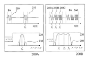
発明者らは、このトレードオフに対処し、ビットの生成に異なる周波数スペクトルを有する複数のパルスを適用する概念的なステップを通じてそれを取り除いた。第1画像200Aの図2Aを参照すると、各ビット210が単一周波数でのパルス発振である従来技術のインパルス無線の時間および周波数領域の概略図が示され、その結果、周波数スペクトルは、規制当局のUWBマスク220によって許可された周波数範囲内で、その周波数範囲内の最大電力以下のf0を中心とする単一のピーク230になる。対照的に、図2Aの第2画像200Bに示されるように、各ビット260は、それぞれ周波数f1、f2、f3にある一連のサブパルス260Aから260Cを含む。したがって、シンボル(ビット260)のマルチパルススペクトル280は、サブパルス260Aから260Cの個々のパルススペクトルを合計することにより概念的に得られ(明確にするために位相スクランブルは省略される)、これにより、帯域幅は増加するが、シンボルの継続時間は増加し、単一パルスの従来技術の方法とは対照的に、UWBマスク220より下で最大電力を維持しながら、受信機で必要とされるタイミング要件および同期レベルを緩和しながらシンボルエネルギーを最大化できるようにする。パラメータの異なるセットを有する任意の数のパルスをバンドル内に含めて、パルススペクトルを特定の要件に合わせ得る。
The inventors addressed this trade-off and removed it through a conceptual step of applying multiple pulses with different frequency spectra to bit generation. Referring to FIG. 2A of the
放射マスクに違反することなく、最大の信号エネルギーを提供するために、パルスの位相はランダム化する必要があり、つまり、周期信号で一般的に見られる「スペクトル線」の生成を避けるために、スペクトルを白色化する必要があり、マルチパルススペクトルが個々のパルススペクトルの合計になるように、パルス間の相関を減らす必要がある。これは、送信機の電力アンプの位相変調に擬似ランダムノイズ(PRN)シーケンスを適用することで実行され得る。受信機は信号の位相に敏感ではないため(後述する非コヒーレント検出方式のため)、これを実現するために送信機と受信機間の位相同期は不要である。送信された信号の正確なスペクトル形状は、各シンボルで異なる周波数と持続時間を有するパルスを生成することにより制御され得る。シンボルまたはビットは、発明者によって「パルスバンドル」を含むと呼ばれる。パルスバンドルのスペクトルは、そのパワーが個々のパルスパワースペクトルの合計であるため、簡単に計算される。これにより、環境の変化やユーザーの要求に応じた動的な再構成が容易になり、さまざまな規制環境での運用も可能になる。 In order to provide maximum signal energy without violating the radiation mask, the phase of the pulse needs to be randomized, that is, to avoid the generation of "spectral lines" commonly found in periodic signals. The spectra need to be whitened and the correlation between the pulses needs to be reduced so that the multi-pulse spectrum is the sum of the individual pulse spectra. This can be done by applying a pseudo-random noise (PRN) sequence to the phase modulation of the transmitter power amplifier. Since the receiver is not sensitive to the phase of the signal (because of the non-coherent detection method described later), phase synchronization between the transmitter and the receiver is not necessary to achieve this. The exact spectral shape of the transmitted signal can be controlled by generating pulses with different frequencies and durations for each symbol. A symbol or bit is referred to by the inventor as including a "pulse bundle". The spectrum of the pulse bundle is easily calculated because its power is the sum of the individual pulse power spectra. This facilitates dynamic reconfiguration in response to changes in the environment and user requirements, and enables operation in various regulatory environments.
信号のパルス性により、帯域外スペクトルサイドローブが存在する。パルスシェーピングによりサイドローブレベルが低下しても、サイドローブの最大値は、平均帯域外パワースペクトル密度よりも数dB高くなり得る。デューティサイクル制御ビットの最下位ビット(LSB)にPRNシーケンスを適用することにより、各パルスの幅をランダムにディザリングし得る。これにより、帯域外スペクトル内のサイドローブとヌルの位置が同等にディザリングされ、帯域外スペクトルがその平均値に効果的にホワイトニングされ、FCCスペクトルマスクに対するマージンが増加する。 Due to the pulse nature of the signal, there is an out-of-band spectral sidelobe. Even if the sidelobe level is reduced by pulse shaping, the maximum sidelobe can be several dB higher than the average out-of-band power spectral density. By applying the PRN sequence to the least significant bit (LSB) of the duty cycle control bits, the width of each pulse can be randomly dithered. This causes the sidelobes and nulls in the out-of-band spectrum to be equally dithered, effectively whitening the out-of-band spectrum to its mean value, and increasing the margin for the FCC spectrum mask.
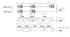
ワイドバンドデータストリームの変調は、例えば図2Bに示すように、オンオフキーイング(On−Off Keying(OOK))またはパルス位置変調(PPM)によって実現され得る。OOK変調2020では、パルスバンドルの存在は「1」を示し、バンドルの不在は「0」を示す。これは、送信機が「1」を送信する場合にのみアクティブである必要があり、データビットが「0」の場合にスリープモードのままにできるため、低電力の通信方式である。また、データはおよそ半分の時間しか送信されないため(適切なデータコーディングにより保証されているため)、通信範囲を広げることができ、これは、各パルスバンドルはより多くのエネルギーを含むことができ、規制機関によって課せられた放射マスクをまだ満たし得ることを意味する。
Modulation of the wideband data stream can be achieved by on-off keying (OK) or pulse position modulation (PPM), for example, as shown in FIG. 2B. In
しかしながら、OOK変調では、受信したデータが「1」か「0」かを判断するために、定義されたしきい値が必要である。これにより、チャネル特性または干渉信号のレベルが急激に変化する環境でのパフォーマンスが低下し得る。これらの状況では、例えば、PPM変調2010が代替変調方式として優先され得る。この場合、「1」または「0」が受信されたかどうかを決定するのは、シンボル期間内のパルスバンドルの位置である。検出器は、本質的にシンボル期間の前半で受信したエネルギーとシンボル期間の後半で受信したエネルギーを比較して決定を下し、急速に変化する環境を補償できるフレームレベルのしきい値を作成する。発明者の設計によると、同じ送信機と受信機のペア内でOOK変調とPPM変調を切り替える機能は、パラレルデジタル化アーキテクチャを備えたバーストモード通信方式を使用することで可能になる。
However, in OK modulation, a defined threshold is required to determine whether the received data is "1" or "0". This can reduce performance in environments where channel characteristics or levels of interfering signals change rapidly. In these situations, for example,
したがって、図2Bには、PPM2010およびOOK2020変調方式のシンボル200Cが示されている。さらに、フレーム構造200Dが示され、ここで、各フレーム200Dの前には、受信機での細かい同期を実現するための同期ブロック2030およびデータ2050が送信/受信される前にシンボル同期のドリフトを修正するための開始ビット2040がある。単純な同期構造のため、短い同期ブロック2030のみが必要であり、システムの有効なデータレートのオーバーヘッドを削減する。フレーム200Dの間では、消費電力を削減するために送信機および受信機の電源が切れる。これにより、開始2060、フレーム200D、およびスリープ2080の得られた構造を有するストリーム200Eが生成される。
Therefore, FIG. 2B shows PPM2010 and the symbol 200C of the OK2020 modulation scheme. Further, a
このような伝送プロトコルは、再構成可能なデータレートにも適している。システム操作の実例として、1Mbpsのデータレート、1Kbitのフレームサイズ、20Mbpsのバーストデータレートを想定する、例えば、フレーム内では、50nsごとにシンボルが送信される。この例では、各フレームの持続時間は50μsである。1Mbpsデータレートを達成するために、フレーム繰り返しレートは1KHzになる、つまり、フレームは1msごとに送信される。これは、受信機は1msごとに50μsに対してのみアクティブになり、5%のデューティサイクルになるであろうことを意味する。同じフレームレートと継続時間で100kbpsのデータレートを実現するには、必要な変更は、フレームの繰り返しレートを10ms(つまり、10msごとに送信されるフレーム)に減らすことだけであろう。これで、受信機は10msごとに50μsに対してのみアクティブになり、0.5%のデューティサイクルになるであろう。したがって、データレートの10倍の削減は、消費電力の10倍の削減にもつながるであろう。 Such transmission protocols are also suitable for reconfigurable data rates. As an example of system operation, a data rate of 1 Mbps, a frame size of 1 Kbit, and a burst data rate of 20 Mbps are assumed. For example, in a frame, a symbol is transmitted every 50 ns. In this example, the duration of each frame is 50 μs. To achieve a 1 Mbps data rate, the frame repeat rate will be 1 KHz, i.e., frames will be transmitted every 1 ms. This means that the receiver will only be active for 50 μs every 1 ms and will have a duty cycle of 5%. To achieve a data rate of 100 kbps with the same frame rate and duration, the only change needed would be to reduce the frame repeat rate to 10 ms (ie, frames transmitted every 10 ms). The receiver will now be active only for 50 μs every 10 ms, resulting in a duty cycle of 0.5%. Therefore, a 10-fold reduction in data rate will also lead to a 10-fold reduction in power consumption.
C:例示的なUWB送信機 C: Illustrative UWB transmitter
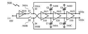
図3を参照すると、本発明の一実施形態による送信機300の概略図が示される。
パルスパターンブロック310は、現在のシンボルを表すために使用されるパルスの構成を保持する。シンボルレートクロック(つまり20MHz)から、遅延ロックループ(DLL)330によって複数のフェーズが生成される。各クロック位相の立ち上がりエッジは、シンボルパルスバンドルの1つのパルスの開始を表す。マルチプレクサ320は、クロック位相のエッジによってトリガーされ、パルスパターンブロック310から現在のパルスの構成を選択する。パルス発生器(パルス)350は、マルチプレクサ320によって設定されたパルス幅でパルスを生成し、デジタル制御発振器(DCO)340および電力アンプ(PA)350を有効にする。有効にすると、DCO 340はマルチプレクサ320によって設定された周波数のガウス型パルスを生成し、PA 360によって増幅され、アンテナ370によって放射される。したがって、パルスパターンブロック310は、シンボルまたはシンボルシーケンスのパルスを確立する。このようにして、パルスパターンブロック310を更新することにより、各シンボルに使用されるパルスシーケンスが調整され、したがって、パルスパターンブロック310は、限定されないが、ネットワーク環境データ、所定のシーケンス、日付、時刻、地理的位置、受信信号の信号対雑音比(SNR)、および規制マスクを含む1つまたは複数の要因に基づいて動的に更新され得る。
Referring to FIG. 3, a schematic diagram of the
The pulse pattern block 310 holds the pulse configuration used to represent the current symbol. From the symbol rate clock (ie, 20 MHz), the delay lock loop (DLL) 330 generates multiple phases. The rising edge of each clock phase represents the start of one pulse in the symbol pulse bundle. The
C1.送信機パルスの生成と整形 C1. Transmitter pulse generation and shaping
DCO 340出力は、所定の周波数および/または振幅特性を離散的にまたはパルサー350の動作と組み合わせて提供するように整形され得る。例えば、本明細書内で説明される本発明の実施形態では、ガウス整形の使用およびガウスパルスを整形する方法が提示され、採用される。この特許内に示される実施形態は、その接地接続の調整を通じてPA 360を介してパルスを整形することを採用している。これにより、送信機はデジタルドメイン全体で動作できるようになり、静的電流の消費を無視できる完全なデジタル構造が可能になる。さらに、完全なデジタル送信機構造の使用により、非常に積極的なパワーサイクリング、つまりパルスレベルでのパワーサイクリングが可能になる。しかしながら、他の実施形態では、代替の整形方法論および整形プロファイルが採用され得る。
The
C2.接地スイッチ式電力アンプ C2. Ground switch type power amplifier
UWB伝送のパルス特性には、パルススペクトルのサイドローブを低減するために、パルス整形で高い瞬時電力レベルを提供できる電力アンプ(PA)が必要である。低い平均消費電力を実現するには、高い電力効率、効率的なパワーサイクリング、高速のウェイクアップ/スリープ遷移時間が必要である。図4に示されるようなスイッチング電力アンプ(SW−PA)400は、UWBパルスバンドルを送信するために、本明細書内で提示される本発明の実施形態内で採用された。したがって、SW−PA400は、図3のPA360の実施形態を表す。図示のように、第1および第2トランジスタM1 410およびM2 420は、その入力がDCOによって生成される相補的なデジタルクロックであるスイッチとして機能し、完全差動SW−PA400を実現することを可能にする。これらのデジタルクロックの周波数は、パルスバンドル内の各個別パルスの中心周波数を設定し、第3トランジスタM3 430に印加されるパルスイネーブル信号は各パルスの持続時間を設定する。したがって、パルスイネーブル/パルス持続時間は、パルス(PULSE)460に結合されたパルサー350によって提供されるパルス信号でありつつ、補完的なデジタルクロックはVCOP440およびVCON450によって提供され、その結果、第3トランジスタM3 430を介したSW−PA400の接地接続がこの信号により修正される。SW−PA400の出力は、RFP470およびRFN480で提供され、SW−PA400は電力レールVDDに結合される。
The pulse characteristics of UWB transmission require a power amplifier (PA) capable of providing high instantaneous power levels with pulse shaping in order to reduce the sidelobes of the pulse spectrum. Achieving low average power consumption requires high power efficiency, efficient power cycling, and fast wake-up / sleep transition times. A switching power amplifier (SW-PA) 400 as shown in FIG. 4 has been adopted within the embodiments of the invention presented herein for transmitting UWB pulse bundles. Therefore, SW-PA400 represents the embodiment of PA360 in FIG. As shown, the first and
対称性により反対側の動作が同一になるため、差動SW−PA 400の片側(半分の回路)のみを考慮することにより、機能が説明され得る。SW−PA400の出力、この場合、RFP470は、第1トランジスタM1 410がオンであるときにGNDPAノードに接続される。SW−PA400出力のDC電圧は(インダクタL1を介して)VDDであるため、第1トランジスタM1 410 M1がオフのとき、SW−PA400出力は、VDD+(VDD−GNDPA)=2×VDD−GNDPAになる。これら2つのケースを組み合わせると、2×VDD−GNDPAの出力スイングが得られる。したがって、GNDPAノードの電圧を整形することにより、SW−PA 400の出力は、出力パルスを生成するためのクロック信号の直接整形された変形例になり得る。設計により、出力パルスは第3トランジスタM3 430およびC5によって整形され、パルス持続時間と帯域幅の間の最適なバランスのためのガウスプロファイルを実現し、パルススペクトルのサイドローブパワーを最小化する。SW−PA400は、電力アンプが静的電力のみを消費することを保証するイネーブルスイッチとして機能する第3トランジスタM3 430によってアクティブ化されると、出力パルスを生成する。
Since the operation on the opposite side is the same due to symmetry, the function can be explained by considering only one side (half circuit) of the differential SW-
C3.デジタル制御発振器 C3. Digitally controlled oscillator
図5に示すような完全差動リングDCO(FDR−DCO)500は、本明細書内で提示される本発明の実施形態内で採用されているため、したがって、FDR−DCO500は図3のDCO340の実施形態を表す。FDR−DCO 500は、図4のSW−PA 400で第1および第2トランジスタM1 510およびM2 520にデジタルクロックを提供し、その動作を切り替えて、SW−PA 400に供給されるクロックを生成するためにパルサー350の出力が供給される。このFDR−DCO500の周波数は、第1および第2キャパシタC1 540AおよびC2 540Bならびに第3および第4キャパシタC3 540CおよびC4 540Dをそれぞれ含む第1および第2キャパシタバンクによって設定され、これらは、それぞれ第1および第2完全差動インバータINV1 510およびINV2 520の出力に接続されている。第3完全差動インバータINV3 530からの出力は、SW−PA400のVOCP440およびVCON450に結合される相補的なデジタルクロックVOCPおよびVCONを提供する。
Since the fully differential ring DCO (FDR-DCO) 500 as shown in FIG. 5 is employed within the embodiments of the invention presented herein, therefore the FDR-
したがって、本発明の一実施形態では、第1から第4キャパシタC1 540AからC4 540Dは、同一の静電容量値を有し、それぞれが4ビットのプログラム可能性を備えたプログラム可能なキャパシタバンクであるが、他のレベルのプログラム可能性などが使用され得る。第3および第4スイッチS3 550AおよびS4 550Bは、パルスが送信されない場合にFDR−DCO 500をオフにして電力を節約するために使用される。第1および第2スイッチS1 560AおよびS2 560Bと連動する第4インバータINV4 570は、発振前に発振器ノードをプリチャージし(FDR−DCO 500がオフの場合)、位相変調用のパルスの極性を制御する。これにより、非常に高速な起動時間(nsの数分の1のオーダー)で発振器が作られ、送信機のパワーサイクリング効率が向上する。パルスを生成する場合、他のすべての時間では、FDR−DCO 500は低電力スリープ状態にありつつ、FDR−DCO 500は、第1および第2スイッチS1 560AおよびS2 560Bを開き、第3および第4スイッチS3 550AおよびS4 550Bを閉じることにより有効になる。必要に応じて、VDDとSW−PA 400の電流分岐の間に追加のPMOSトランジスタを追加して、パルスの終わりにSW−PA 400を迅速にオフにし、パルス整形を改善し得る。
Therefore, in one embodiment of the invention, the first to
C4.パルス発生器 C4. Pulse generator
DCO340、例えば FDR−DCO 500、およびPA360、例えば、SW−PA 400、に結合されたパルサー350からのパルス信号は、パルス生成回路を使用して生成される。したがって、図6に示されるパルス発生器(PULGEN)600は、本明細書内で提示される本発明の実施形態内で採用されているため、したがって、PULGEN600は図3のパルサー350の実施形態を表す。図示されているように、入力信号は、第1および第2インバータINV 1 610およびINV 2 620を介してANDゲート650に直接および間接的にルーティングされる。第1および第2のインバータINV1 610およびINV2 620は、プログラム可能なキャパシタバンクである第1および第2キャパシタC1 630およびC2 640と組み合わせた可変遅延回路の一部であるが、他のレベルのプログラム可能性などを使用し得る。したがって、DATAラインの立ち上がりエッジにより、この回路はnsオーダーのパルスを作る。パルス幅は、第1および第2キャパシタC1 630およびC2 640によって生成される可変遅延の関数であり、デジタル的に調整可能であることにより、パルス幅をデジタル的にプログラムし得る。
The pulse signal from the
D.例示的なUWB受信機 D. Illustrative UWB receiver
図7を参照すると、本発明の一実施形態による受信機700の概略図が示される。アンテナ710からのRF信号は、低ノイズアンプ(LNA)720によって最初に増幅された後、2段階RFアンプ(AMP1)730に渡される。最初のスクエアリングミキサ(MIX1)740は、信号とそれ自体を乗算して、中間周波数(IF)に変換する。3段階の可変ゲインアンプ(VGA)750は、信号をさらに増幅し、バンドパスフィルタ機能を実行する。次に、VGA 750出力は、信号をベースバンド周波数にダウンコンバートする第2スクエアリングミキサ(MIX2)760に結合される。並列積分器(INT1およびINT2)は信号エネルギーを合計し、デジタルプロセッサ内のアナログ−デジタル(A/D)コンバーター(ADC1およびADC2)によってデジタル化される(明確にするために示されていないが、例えば図12に関して以下のデジタルプロセッサ(DIGIPRO)1200に関して説明される)。
Referring to FIG. 7, a schematic diagram of the
D1.受信機検出と干渉除去 D1. Receiver detection and interference elimination
全体のスペクトルはより広い帯域幅、例えば、パルスバンドル戦略を介してBW=3GHzに対する3GHz≦f≦6GHzをカバーしつつ、受信機のIFチェーンは、個々のパルス帯域幅のオーダーである瞬時帯域幅、例えば、500MHzを利用する。これにより、パルスダウンコンバージョン後の回路ブロックの低消費電力が可能になるが、それでもなお通信に超広帯域のスペクトルが使用され得る。UWB信号の受信機は、目的の信号の帯域幅が広く、高帯域幅の受信機チェーンを必要とするため、困難がある。さらに、狭帯域内干渉、DCオフセット、および1/fノイズの発生も、低電力実装では問題がある。したがって、IF段階では次のことが望ましいであろう。
・DCオフセットの問題を回避するために、準低IFアーキテクチャで動作する。
・RFセクションの1/fノイズを減らす。
・システムの堅牢性と干渉除去を向上させるために、典型的な狭帯域干渉(例えば、BW<50MHzの信号)を除去する。
The IF chain of the receiver is on the order of the individual pulse bandwidths, while the overall spectrum covers a wider bandwidth, eg, 3 GHz ≤ f ≤ 6 GHz for BW = 3 GHz via a pulse bundle strategy. For example, 500 MHz is used. This allows for low power consumption of the circuit block after pulse down conversion, but still allows ultra-wideband spectra to be used for communication. UWB signal receivers are difficult because they have a wide bandwidth for the signal of interest and require a high bandwidth receiver chain. Further, in-band interference, DC offset, and 1 / f noise generation are also problems in low power implementations. Therefore, at the IF stage, the following would be desirable.
-Operates on a semi-low IF architecture to avoid DC offset issues.
-Reduces 1 / f noise in the RF section.
• Eliminates typical narrowband interference (eg, BW <50 MHz signal) to improve system robustness and interference elimination.
これを達成するために、受信機700内にハイパスデカップリングキャパシタを指定して、このプロセス中にわずかな量の所望のパルスエネルギーが確実に遮断されるようにする。さらに、これは、完全な感度を保持するために、IF段階の後の第2スクエアリング段階と結合される。受信機のエネルギー検出感度/ノイズ除去の強化と整流信号の生成のための二重スクエアリング法は、CMOS統合に良く適している。この二重スクエアリング法は、受信信号のインパルス特性を利用して、各インパルスの非線形処理と効果的に同等であるため、検出を強化する。第2スクエアリング演算では、他の従来のインパルス無線受信機で行われているように、検出された振幅/ピークを単に使用する代わりに、ダウンコンバートされたパルスエネルギー全体を使用して検出の確率を高めるようにしつつ、第1スクエアリング演算は、受信パルスを準低IF信号にダウンコンバートする。前述のように、2つのスクエアリング演算間のハイパスフィルタリングにより、DCオフセットの軽減、1/fノイズの低減、および狭帯域干渉除去が行われる。
To achieve this, a high pass decoupling capacitor is specified in the
図7に関して提示された非コヒーレント受信機アーキテクチャは、周波数同期、または送信機によって使用されるパルス位相/周波数パターンの知識を必要としないことが有益であることは、当業者には明らかであろう。 It will be apparent to those skilled in the art that the non-coherent receiver architecture presented with respect to FIG. 7 does not require knowledge of frequency synchronization, or the pulse phase / frequency pattern used by the transmitter. ..
D2.低ノイズアンプ D2. Low noise amplifier
図8に示されるような低ノイズアンプ(LNA)800は、本明細書内で提示される本発明の実施形態内で採用されているため、したがって、LNA800は図7のLNA720の実施形態を表す。差動入力信号RFpおよびRFnは、それぞれ第3および第4のキャパシタC3 850AおよびC4 850Bを介して、VBIASによってゲートにバイアスがかけられ、そのバイアス電流はインダクタL1を介してグランドにシンクされる、一対の共通ゲートトランジスタM1 810およびM2 820のドレインに結合される。M1 810およびM2 820のドレインで、増幅された信号の帯域幅を増加させるために、インダクタL2 870とともに抵抗器R1 830およびR2 840によってシャントピーキング(shunt peaking)が実行される。信号は、第1および第2キャパシタC1 860AおよびC2 860BによってLNA800から出力ポートOUTPおよびOUTNに結合される。
Since the low noise amplifier (LNA) 800 as shown in FIG. 8 is employed within the embodiments of the invention presented herein, the
D3.スクエアリングミキサ D3. Square ring mixer
図9に示されるようなスクエアリングミキサ(SQ−MIX)900は、本明細書内に提示される本発明の実施形態内で採用されているため、したがって、SQ−MIX900は、図7の第1および第2スクエアリングミキサMIX1 740およびMIX2 760の実施形態を表す。示されるように、差動入力信号INPおよびINNは、トランジスタM7 910およびM8 920のゲートに結合され、その相互コンダクタンスは信号を差動ドレイン電流に変換する。同時に、入力信号は、交差結合されたトランジスタペアM3:M4およびM5:M6にも結合され、それらは、ドレイン電流をSQ−MIX 900の正(OUTP)側または負(OUTN)側のいずれかに誘導し、それにより入力にそれ自体を乗算、すなわちそれを二乗する。トランジスタM1およびM2は、出力で最大電圧ゲインを提供するために、電流源950としてバイアスされる。入力信号に結合され、キャパシタC1からC4および抵抗器R1からR4を含むバイアス回路960は、NMOSトランジスタが適切なバイアスポイントにバイアスされることを保証する。
Since the square ring mixer (SQ-MIX) 900 as shown in FIG. 9 is adopted in the embodiment of the present invention presented herein, therefore, the SQ-
D4.可変ゲインアンプ D4. Variable gain amplifier
図10に示されるような可変ゲインアンプゲイン段階(VGA−GS)1000は、本明細書内で提示される本発明の実施形態内で採用されているため、したがって、VGA−GS1000は、図7のVGA750内の各ゲイン段階の実施形態を表す。差動入力信号INPおよびINNは、それぞれ複合トランジスタペアM1:M2およびM3:M4のゲートに結合される。ソースおよびドレイン、ならびにそれらのゲートが接続されたトランジスタ1075(1)から1075(N)から形成されたトランジスタアレイ1070を含むインサートに示される各複合トランジスタM1からM4は、スイッチの位置に応じて、信号またはグランドのいずれかに接続され得る。従って、複合トランジスタペアM1:M2およびM3:M4は切り替え可能な相互コンダクタンスを有する。正側(OUTP)の実効相互コンダクタンスはM1とM3の相互コンダクタンスの差に等しく、負側(OUTN)はM2とM4の相互コンダクタンスの差に等しい。したがって、ゲインは複合トランジスタのスイッチ位置によって調整され得る。トランジスタM6およびM7は、電流源1030としてバイアスされ、出力電圧ゲインを最大化する。キャパシタC3およびC4は出力ノードでローパスフィルタリングを実行し、キャパシタC1およびC2とバイアス抵抗器R1およびR2は入力ノードでハイパスフィルタリングを実行する。したがって、VGA−GS 1000は有効なバンドパスフィルタ応答で動作する。
Since the variable gain amplifier gain step (VGA-GS) 1000 as shown in FIG. 10 is employed within the embodiments of the invention presented herein, therefore, the VGA-
E.送信機−受信機の同期とクロッキング E. Transmitter-receiver synchronization and clocking
上で説明したように、UWB通信リンクの受信機(Rx)と送信機(Tx)は、他の無線プロトコル内とは異なり、分散タイミング情報を介して互いに同期していない。したがって、各回路の要件は、本発明の実施形態による無線インパルス無線の極めて積極的なデューティサイクルを維持し、それによりインパルス無線通信に固有のエネルギー効率を維持するためのTxとRx間の効率的な同期である。したがって、本発明者らは、超低スリープモード電力消費のためのデュアルクロックタイマーシステムを含む専用同期ハードウェアを使用して、低遅延送信機/受信機同期方法/アルゴリズムを確立した。これにより、無線の非常に積極的なデューティサイクルを維持するためにTxとRxとの間の効率的な同期が可能になり、インパルス無線通信に固有のエネルギー効率が維持される。 As described above, the receiver (Rx) and transmitter (Tx) of the UWB communication link are not synchronized with each other via distributed timing information, unlike within other radio protocols. Therefore, the requirement of each circuit is the efficiency between Tx and Rx to maintain the highly aggressive duty cycle of the radio impulse radio according to the embodiment of the invention, thereby maintaining the energy efficiency inherent in the impulse radio communication. It is a good synchronization. Therefore, we have established a low delay transmitter / receiver synchronization method / algorithm using dedicated synchronization hardware including a dual clock timer system for ultra-low sleep mode power consumption. This allows efficient synchronization between Tx and Rx to maintain a very aggressive duty cycle of the radio and maintains the energy efficiency inherent in impulse radio communication.
マルチフェーズクロックベースバンドトランシーバーは、クロック周波数(例えば、200MHzの代わりに20MHz)を下げ、電力効率を高めるために設計された。さらに、並列化されたADC/積分器構造、図12AのDIGIPRO 1200が採用され、より高速な同期と干渉検出の強化が可能になった。この構造により、受信タイムフレーム中に完全な信号を観測し得る。この構造により、動的に変化する変調方式(OOK、PPMなど)も可能になり、チャネルまたは規制環境に基づいて通信の堅牢性が向上する。
Multi-phase clock baseband transceivers have been designed to lower the clock frequency (eg 20MHz instead of 200MHz) and increase power efficiency. In addition, a parallel ADC / integrator structure,
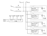
E1.低電力クロック発生器 E1. Low power clock generator
図11を参照すると、本明細書内で提示される本発明の実施形態内で採用され得る第1クロック発生器(CLKGEN1)1100が示され、したがって、CLKGEN1 1100は、図7の受信機700内の送信機300およびDIGIPRO1200に20MHz信号を提供する。低電力クロック発生器CLKGEN1 1100は、水晶XTAL 1110、抵抗器R1、キャパシタC1およびC2とともに、低周波発振器、つまり32 kHzとして機能するインバータINV1 1120を含む。正弦波発振器信号は、インバータINV2 1125によって方形波クロックに増幅され、フェーズドロックループ(Phased Lock Loop(PLL))1190で基準として使用される。PLL 1190は電圧制御発振器(Voltage Controlled Oscillator(VCO))1150で構成され、その出力は分周器1180で周波数が分周され、位相検出器1130で基準と比較される。分周クロックの周波数が基準より低いか高いかに応じて、DOWNまたはUPのパルスが生成される。チャージポンプ1140は、抵抗器R2とキャパシタC3およびC4とともに、UP信号とDOWN信号をVCOの制御信号にフィルタリングする。ロックすると、ループは基準クロックの整数倍であるインバータINV3 1160によってバッファーされた出力クロックを生成する。
Referring to FIG. 11, a first clock generator (CLKGEN1) 1100 that can be employed within the embodiments of the invention presented herein is shown, and thus the
上記のように、UWBトランシーバでのクロック生成と同期の効率的な実装は、低電力動作に不可欠である。ナノ秒のオーダーのパルス幅では、従来の簡単な合成デジタル手法では、関連する動的消費電力が高く、数百MHz以上のベースクロックが必要になる。水晶クロックジェネレーターでベースクロックを直接生成すると、電力消費が比較的高くなる。水晶発振器の電力は周波数に直接比例するため、水晶発振器をはるかに低い周波数(例えば32kHz)で動作させ、周波数にフェーズドロックループ(PLL)を掛けると、電力消費が大幅に削減される。この戦略は、UWBトランシーバでの低電力クロック生成のために発明者によって利用される。デジタルロジックのベースクロックは、シンボル周波数、例えば、20MHzに設定され、これは、シンボルがデジタルベースバンドハードウェアによって処理され、低電力低周波発振器XTAL 1110を利用した図11のCLKGEN1 1100などのクロック発生器によって生成されるレートである。次に、図3の送信機300に関して示されるように、20MHzクロックは、ナノ秒範囲の間隔でこのクロックから複数の位相を導出する遅延ロックループ(DLL)330に結合され、これらは、マルチプレクサ320、DCO 340、およびパルサー350とともにシンボルパルスを生成するタイミングベースとして使用される。パルス発生器の制御信号は、DLLの多相クロックのエッジで、パルスパターン310のメモリから制御ビットを選択するマルチプレクサによって生成される。
As mentioned above, an efficient implementation of clock generation and synchronization in UWB transceivers is essential for low power operation. With pulse widths on the order of nanoseconds, traditional simple synthetic digital techniques have high associated dynamic power consumption and require a base clock of several hundred MHz or higher. Generating the base clock directly with a crystal clock generator results in relatively high power consumption. Since the power of the crystal oscillator is directly proportional to the frequency, operating the crystal oscillator at a much lower frequency (eg 32 kHz) and applying a phased lock loop (PLL) to the frequency will significantly reduce power consumption. This strategy is utilized by the inventor for low power clock generation in UWB transceivers. The base clock of the digital logic is set to a symbol frequency, eg, 20 MHz, which is the clock generation such as
PLL 1190の起動時間はミリ秒の範囲であり、ループを安定させるために必要な水晶発振器サイクルの数によって事実上制限される。50kbbsよりも高いデータレートでは、PLL 1190とDLL 330はフレーム間でオンのままであり、低消費電力に最適化されている。50kbbs以下のデータレートでは、PLL 1190およびDLL 330の両方をフレーム間で電力サイクルし得、スリープモード中の唯一の電力消費は水晶発振器からである。
The startup time of the
E2.同期 E2. Sync
UWBリンクの送信方法にはクロックデータが送信されていないため、受信機クロックの同期が必要であることは明らかである。したがって、図12に関して示されているように、同期ブロック1230は、図7に示されている受信機700のDIGIPRO1200とともに使用される。図12Aに示すように、DIGIPRO 1200は、ダブルエッジトリガー積分器とアナログ−デジタルコンバーター(ADC)ブロックのペアを含む。第1および第2積分器1210Aおよび1210Bのそれぞれは、シンボル周期の半分にわたって積分し、その出力は、第1および第2ADC1220Aおよび1220Bのうちの1つでデジタル化される。第1および第2積分器1210Aおよび1210BはそれぞれCLK1 1240AおよびCLK3 1250Aを介してクロックされ、一方で、第1および第2ADC1220Aおよび1220BはそれぞれCLK2 1240BおよびCLK4 1250Bを介してクロックされる。第1および第2積分器1210Aおよび1210Bのそれぞれは、例えば、3ビットフラッシュADCであり得る。2つの積分器ADCブロックは、シンボルごとに合計4つのオーバーラップする積分ウィンドウが利用できるように、1/4シンボル周期分オフセットされる。これは図12Bで明らかである。
Since no clock data is transmitted in the UWB link transmission method, it is clear that receiver clock synchronization is required. Therefore, as shown with respect to FIG. 12, the
同期フレームブロック中の同期は、受信機のクロック同期が原則として1つの同期シンボルで達成されるように、最大エネルギーで積分ウィンドウを決定することにより達成される。実際には、無線リンクのチャネルの変化を追跡する可変ゲインループを考慮するために、さらなる同期シンボルが必要である。PPM復調は、各シンボルの最大エネルギーで積分ウィンドウを観察することにより達成され、OOK変調は、固定積分ウィンドウでエネルギーを観察することにより達成される。 Synchronization during a synchronization frame block is achieved by determining the integration window with maximum energy so that clock synchronization of the receiver is achieved in principle with one synchronization symbol. In practice, additional synchronization symbols are needed to take into account variable gain loops that track changes in the channels of the radio link. PPM demodulation is achieved by observing the integration window at the maximum energy of each symbol, and OK modulation is achieved by observing the energy in the fixed integration window.
F.エネルギー検出器付きN−パスフィルタF. N-pass filter with energy detector
図7に示すように、本発明の実施形態による例示的なUWB受信機700が示され、アンテナ710からのRF信号は、2段階RFアンプ(AMP1)730に渡される前に低ノイズアンプ(LNA)720によって最初に増幅される。第1スクエアリングミキサ(MIX1)740は、3段階の可変ゲインアンプ(VGA)750が信号をさらに増幅する前に、信号をそれ自体で乗算して中間周波数(IF)に変換する。次に、VGA 750出力は、信号をベースバンド周波数にダウンコンバートする第2スクエアリングミキサ(MIX2)760に結合され、並列積分器(INT1およびINT2)は信号エネルギーを合計し、それはデジタルプロセッサ内のアナログ−デジタルコンバーター(ADC1およびADC2)によってデジタル化される。
As shown in FIG. 7, an
以下スクエアラーと呼ばれるスクエアリングミキサ(MIX2)760は、信号振幅のスクエアリングを実行し、並列積分器によって統合されると、受信信号の瞬間エネルギーを生成する。一定期間の積分は、その期間内のシンボルの総エネルギーをもたらす。しかしながら、干渉信号のノイズおよび積分エネルギーの両方を削減するために、入力信号を対象帯域に制限するように入力信号をフィルタリングする必要がある。図7の例示的なUWB受信機内で、VGA750は、帯域通過フィルタリング機能を提供する適切な設計を介してこれを提供した。しかしながら、消費電力に実質的な影響を与えず、バンドストップフィルタとバンドパスフィルタとを可能にしつつ、増幅機能とフィルタリング機能を分離して、それぞれを独立して最適化できると便利であろう。
The square ring mixer (MIX2) 760, hereinafter referred to as a squarer, performs squared signal amplitudes and, when integrated by a parallel integrator, produces instantaneous energy for the received signal. The integration over a period of time yields the total energy of the symbol within that period. However, in order to reduce both the noise and the integrated energy of the interference signal, it is necessary to filter the input signal so as to limit the input signal to the target band. Within the exemplary UWB receiver of FIG. 7, the
従来技術のフィルタでは、特に中間周波数(Intermediate Frequency(IF))バンドパスフィルタが必要な場合、通常、回路設計者に高い消費電力と低い品質係数を提示する。したがって、本発明者らは、スクエアラー(squarer)の前にスイッチトキャパシタNパスフィルタを組み合わせることに基づいた設計方法論を確立した。明らかになるNパスフィルタは、バンドパスまたはバンドストップフィルタであり、パッシブミキサー構造のローパスフィルタのアップ/ダウン変換に基づく。ローパスフィルタがより高い周波数にアップコンバートされ、中心周波数がクロック周波数によって調整できるため、品質係数は高くなり得る。ただし、Nパスフィルタの欠点は、同期受信機構造で高品質のクロックを生成するために必要なクロック発生器の消費電力が高いことである。これにより、この技術は通常、従来技術内の低電力アプリケーションにはあまり適していない。 Conventional filters typically offer circuit designers high power consumption and low quality coefficients, especially when an intermediate frequency (IF) bandpass filter is required. Therefore, we have established a design methodology based on combining a switched capacitor N-pass filter before a squarer. The N-pass filter to be revealed is a band-pass or band-stop filter, which is based on the up / down conversion of a low-pass filter having a passive mixer structure. The quality factor can be high because the lowpass filter is upconverted to a higher frequency and the center frequency can be adjusted by the clock frequency. However, the drawback of the N-pass filter is the high power consumption of the clock generator required to generate a high quality clock in the synchronous receiver structure. This is why this technique is usually not well suited for low power applications within prior art.
しかしながら、本発明者らは、クロックジッタに関してNパスフィルタの欠点を回避する手段を確立し、その結果、低電力クロック発生器が、Nパスフィルタに関連する従来技術の高電力高精度(低ジッタ)クロック発生器ではなく、Nパスフィルタに使用され得る。クロックジッタの影響は、入力信号のエネルギーをより広い帯域幅に分散させることであり、これにより同期受信機の帯域内エネルギーが削減される。しかしながら、本発明の実施形態による例示的なUWB受信機内では、Nパスフィルタが非同期受信機とペアになっている場合、例えば、図9に示すようなエネルギー検出器、エネルギー検出器がNパスフィルタータイミングクロックの周波数拡散の影響を受けないため、信号のエネルギー全体がキャプチャされる。 However, we have established a means of avoiding the shortcomings of N-pass filters with respect to clock jitter so that the low-power clock generator has the high-power, high-precision (low-jitter) of the prior art associated with N-pass filters. ) Can be used for N-pass filters instead of clock generators. The effect of clock jitter is to distribute the energy of the input signal over a wider bandwidth, which reduces the in-band energy of the synchronous receiver. However, in the exemplary UWB receiver according to the embodiment of the present invention, when the N-pass filter is paired with the asynchronous receiver, for example, the energy detector and the energy detector as shown in FIG. 9 are N-pass filters. The entire energy of the signal is captured because it is not affected by the frequency spread of the timing clock.
この技術は、例えばDC周辺の信号をダウンコンバートするために、セルフミキサー(self−mixer)としてスクエアラーを使用するシステムにも拡張され得る。このシナリオでは、Nパスフィルタによってスクエアラーの選択性が改善されるが、クロックジェネレーターは緩和した量のジッタを示し得るため、電力をあまり消費しない。 This technique can be extended to systems that use a squarer as a self-mixer, for example to downconvert signals around the DC. In this scenario, the N-pass filter improves the selectivity of the squarer, but the clock generator can show a relaxed amount of jitter and therefore consumes less power.
F.1実装例 F. 1 Implementation example
図13Aおよび13Bを参照すると、バンドパスおよびバンドストップの両方の変形例についての本発明の例示的な実装が示される。図13Aを検討すると、受信機フロントエンド1360は、例えば、アンテナ、LNA、RFアンプ、VGAが信号をさらに増幅する前に、信号をそれ自体で乗算して中間周波数(IF)に変換する第1スクエアリングミキサを含む。VGAの出力は、クロック発生器(CLK Gen)1320によって駆動されるNパスフィルタ1310に結合され、Nパスバンドパス(NP−BP)フィルタ1310の出力は、次いで、スクエアラー1330に結合され、その後、例えば積分器1340を含む後続の受信機回路に結合される。図13Bでは、同じ全体的な受信機回路構成が描かれているが、Nパスバンドパスフィルタ1310はNパスバンドストップフィルタ(NP−BS)1350に置き換えられる。
Referring to FIGS. 13A and 13B, exemplary implementations of the invention for both bandpass and bandstop variants are shown. Considering FIG. 13A, the receiver
図14は、本発明の一実施形態によるNP−BP1310の例示的な設計を示しており、フィルタリングされる受信信号、VINは、それぞれNパス1410Aから1410Nに結合されている。各パスは、入力スイッチSX1(X=1、2、・・・・、N)、フィルタFX(X=1、2、・・・・、N)、および出力スイッチSX2(X=1、2、・・・・、N)で構成されている。Nパス1410Aから1410Nからの出力は、それぞれ組み合わされて、フィルタリングされた出力VOUT、を提供する。フィルタFXは、ローパスフィルタまたはバンドパスフィルタである。
FIG. 14 shows an exemplary design of the NP-BP1310 according to an embodiment of the invention, in which the filtered received signal, VIN, is coupled to
図14に示されたNP−BPは図15Aに示されており、各電気スイッチに印加されるクロック信号と個々のフィルタFxの例示的なRCフィルタ設計が示されている。図示されているように、入力および出力電気スイッチは、それぞれ各NP−BP 1510AからNP−BP 1510N内で駆動され、それぞれ同じクロック信号よって駆動される、例えば、CLK0を含むNP−BP 1510A、CLK1を含むNP−BP 1510Bなどから、CLKN−1を含むBP−NP 1510Nまで。スイッチの各ペアの間には、スイッチのペア間に直列に接続された抵抗器Rと、グランドに並列に接続されたキャパシタCx(X=1、2、・・・・、N)を含むRCフィルタがある。クロック信号は図15Bに示されているが、図15Cは単一の抵抗器RがNパスへの分割の前に配置されている第1実装の簡略化を示す。図16は、NP−BPが片面設計として実装されている、さらなる実装の簡略化を示す。したがって、入力は、そのクロック信号CLKY(Y=0、1、・・・・、N−1)および関連するキャパシタCx(X=1、2、・・・・、N)によって駆動される単一のスイッチを含むNパスに結合される。今や、出力はすべてのパスと入力の間の共通点である。
The NP-BP shown in FIG. 14 is shown in FIG. 15A, showing an exemplary RC filter design for the clock signal applied to each electrical switch and the individual filter Fx. As shown, the input and output electrical switches are driven within each NP-BP 1510A to NP-
スクエアリングミキサ(SQ−MIX)900を備えたスクエアラー1330の例示的な実装を図9に示す。これは差動スクエアラーの実装であるため、図17に示すような差動Nパスフィルタに結合され得る。したがって、図16に示すような一対のNP−BP片側フィルタが示されており、それぞれがNスイッチおよびキャパシタを備えた入力抵抗器Rを含む。図17N=4内では、キャパシタC1;C2;C3;C4を備えた4つの並列パス1710Aから1710Dが示されており、ここで、差動回路は、スイッチによって各差動入力に結合された単一のキャパシタを使用する。これらのスイッチは、CLK(θ=0°);CLK(θ=90°);CLK(θ=180°);CLK(θ=270°)として示されるクロック信号の適切な位相によって駆動される。これらのクロックは、クロック発生器回路からそれに結合された差動クロックから4段階クロック発生器1720によって生成されている。
An exemplary implementation of the
図18は、図16に示したものと同等のバンドストップフィルタ設計を示しており、バンドストップフィルタは今、抵抗器Rと直列のキャパシタCx(X=1、2、・・・・、N)を含む。 FIG. 18 shows a band-stop filter design equivalent to that shown in FIG. 16, where the band-stop filter is now a capacitor Cx (X = 1, 2, ..., N) in series with the resistor R. including.
G.UWBインパルス無線(Impulse Radio)による測距と測位G. Distance measurement and positioning by UWB impulse radio (Impulse Radio)
前述のように、距離測定と位置/位置測定は、UWBトランシーバを使用するデバイス/サブシステム/システム/コンポーネントなどの多くのアプリケーションの1つの態様である。そのようなデバイス/サブシステム/システム/コンポーネントなどの追加のハードウェア機能内でUWBベースの技術を利用していないことは、別の無線技術、例えば、Bluetooth、Wi−Fi、WiMAXなどのマイクロ波/RF無線システムのある外部環境において内部/外部環境の両方をカバーするものの内部アプリケーション向けのローカルに基づく光学/RF/マイクロ波、または全地球測位システム(GPS)/無線三角測量などを使用して、所望の距離測定と位置/位置測定を実現するために、関連する消費電力などとともに提供されなければならない。 As mentioned above, distance measurement and position / position measurement are one aspect of many applications such as devices / subsystems / systems / components that use UWB transceivers. Not utilizing UWB-based technology within additional hardware features such as devices / subsystems / systems / components is another wireless technology, such as microwaves such as Bluetooth, Wi-Fi, WiMAX. / Using locally based optical / RF / microwave for internal applications, or Global Positioning System (GPS) / Radio Triangulation, etc., which covers both internal / external environment in an external environment with an RF wireless system. , Must be provided with associated power consumption etc. to achieve the desired distance measurement and position / position measurement.
したがって、発明者らは、いずれも参照により本明細書に組み込まれる、WO / 2016/191851「Systems and Methods for Spectrally Efficient and Energy Efficient Ultra−Wideband Impulse Radios with Scalable Data Rates」およびWO / 2015/103692「Systems relating to Ultra−Wideband Broadcasting comprising Dynamic Frequency and Bandwidth Hopping」内で説明および図示されるものと一緒に、この特許出願内で彼らが開発した低電力パルスベースのUWB送信機/受信機/トランシーバを活用した2つの技術を確立した。 Accordingly, the inventors are incorporated herein by reference to WO / 2016/191851 “Systems and Methods for Specterrly Effective and Energy Effective Effect Ultra-Wideband / Wideband / Wideband10 Systems reluting to Ultra-Wideband Broadcasting Dynamic Friend and Bandwise Hopping, along with those described and illustrated in this patent application, the low power pulse-based U We have established two technologies.
F.1 飛行距離測定の時間(同期UWBトランシーバーペア) F. 1 Flight distance measurement time (synchronous UWB transceiver pair)
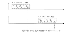
この距離測定システムは、UWB通信リンクに関して説明されており、例示的な20Mbpsの無線データレートと組み合わせて革新的なエネルギー検出方式を活用している。UWBトランシーバの高度な同期スキームの機能を活用して、堅牢な通信とパルスバンドルの追跡を確保し、測距スキームを使用して到着時に「ズームイン」する。 This distance measurement system is described for UWB communication links and utilizes an innovative energy detection scheme in combination with an exemplary 20 Mbps radio data rate. Leverage the capabilities of the UWB transceiver's advanced synchronization scheme to ensure robust communication and pulse bundle tracking, and use the ranging scheme to "zoom in" on arrival.
UWBトランシーバ/受信機に加えて、集積回路(IC)実装またはハイブリッド実装には、図19に従って説明および図示されている測距回路が必要である。所望の測距推定の許容範囲/精度に応じて、センチメートル範囲での測距推定を可能にするためにより高い精度のタイミング基準が必要になる場合があります。 In addition to UWB transceivers / receivers, integrated circuit (IC) or hybrid implementations require ranging circuits described and illustrated according to FIG. Depending on the tolerance / accuracy of the desired range estimation, more accurate timing criteria may be required to enable range estimation in the centimeter range.
システムブロック図の簡略版と簡略化されたパルス列を図19に示す。入ってくるパルス列は、ポストアンテナ1910を通過し、低ノイズアンプ(LNA)1920を通過する。増幅された受信信号の一部は、相関器回路1940に結合され、残りは受信機フロントエンド回路1930の残りに伝播する。相関器回路1940は、受信信号を、パルス発生器1970によって駆動される基準パルス発生器1960によって提供される基準パルスと相関させる。パルス発生器1970自体は、発明者によって確立された本発明の実施形態による公称20Mb/sのUWB方式に対して0.5ns間隔の約50タップを有する遅延ロックループ(DLL)1990を通じて駆動される。DLL1980は、精密基準クロック 1990によって駆動される。相関器回路1940からの出力はタイマー回路に送られる。
A simplified version of the system block diagram and a simplified pulse train are shown in FIG. The incoming pulse train passes through the post-antenna 1910 and the low noise amplifier (LNA) 1920. A portion of the amplified received signal is coupled to the
パルスバンドルの構成により、パルス列内のすべてのパルスの中心周波数が異なるため、入力パルス列内の1つのパルスのみが基準(またはテンプレート)パルスと一致するだろう。これは、本発明の実施形態に関して上記で示し説明したようなUWBエネルギー検出器受信機が、完全なパルス列のエネルギーを統合して通信距離を増加させるという利点を依然として引き出すことができることを意味し、一方で、測距部分は、単一パルスで「ズームイン」してタイミング分解能を向上させ得る。 Due to the configuration of the pulse bundle, the center frequency of all pulses in the pulse train will be different, so only one pulse in the input pulse train will match the reference (or template) pulse. This means that UWB energy detector receivers as shown and described above for embodiments of the present invention can still take advantage of integrating the energy of the complete pulse train to increase communication distance. On the other hand, the ranging portion can be "zoomed in" with a single pulse to improve timing resolution.
本発明の実施形態による例示的なプロセスは、タップ#1で開始し、各パルスバンドルの後、相関ピークが確立されるまでタップが進められるだろう。エネルギー検出受信機は、パルスバンドルの「位置」を25ns以内にすでに知っているため、検索スペースが大幅に削減される。これにより、ハードウェアの複雑さ、検索時間などが大幅に削減される。
An exemplary process according to an embodiment of the invention will start with
F1.1 飛行アルゴリズムの時間F1.1 Flight Algorithm Time
本発明の実施形態によるこの例示的なアルゴリズムは、一対のUWBトランシーバが既に同期されていることを前提としていることに留意することが重要である。参考のために図20に簡略化したタイミング図を示し、図21に本発明の実施形態によるアルゴリズムの例示的なプロセスフローを示す。この例示的なアルゴリズムの多くの変形が可能であることは、当業者には明らかであろう。基本的な精度は、トランシーバで利用可能な基準の精度に依存し、サブナノ秒レベルの精度/ドリフトが推奨される。 It is important to note that this exemplary algorithm according to an embodiment of the invention assumes that the pair of UWB transceivers are already synchronized. For reference, FIG. 20 shows a simplified timing diagram, and FIG. 21 shows an exemplary process flow of the algorithm according to the embodiment of the present invention. It will be apparent to those skilled in the art that many modifications of this exemplary algorithm are possible. The basic accuracy depends on the accuracy of the reference available on the transceiver, and sub-nanosecond level accuracy / drift is recommended.
次に図21を参照すると、プロセスはステップ2105から2150を含む。ステップ2105から2125は以下を示す。
・ステップ2105:UWBトランシーバーペア(UWB#1とUWB#2)を同期する。
・ステップ2110:UWBチップ#1は、UWBパルスバンドルで構成されるパケットを送信する。
・ステップ2115:UWBチップ#1タイマー(TC1)は、最後のパルスバンドルの送信中に開始される。
・ステップ2120:UWB#2がパケットを受信し、相関器回路1940/DLL回路1990が適切なパルスに同期する。
・ステップ2125:UWB#2は、最後のバンドル内の同期パルスが受信されるとタイマーを開始する。
Next, referring to FIG. 21, the process comprises
Step 2105: Synchronize the UWB transceiver pair (
Step 2110:
Step 2115: The
Step 2120:
Step 2125:
その後、以下を含むステップ2130から2150が実行される。
・ステップ2130:UWB#2は、両方のトランシーバに既知の正確な時間を待機する。(注意:チップ#2は、パケット長がわかっているため、最後のバンドルがいつ発生するかを認識する。)
・ステップ2135:正確な待機時間の後、チップ#2は同じタイプのパケットをチップ#1に送り返す。
・ステップ2140:ここで、チップ#1は同じ同期プロセスを実行する。
・ステップ2145:チップ#1は、パケットの最後のバンドルが到着したことを判断し、そのTC1タイマーを停止して経過時間、TC1ELAPSEを生成する。
・ステップ2150:チップ#1は、以下の式(1)および測距距離に基づいて飛行時間(TOF)を決定する。
TC1ELAPSE=TOF+既知の待機時間+TOF+パケット長 (1)
Then steps 2130-2150 are performed, including:
Step 2130:
Step 2135: After an exact wait time,
Step 2140: Here,
Step 2145:
Step 2150:
TC1 ELAPPSE = TOF + known wait time + TOF + packet length (1)
任意に、チップ#1は、相関器が適切なパルスを検出するとすぐにタイマーを停止し、TOF計算で「パケット長」を使用する代わりに、それは「相関前のバンドル数」を使用し得る。これにより、タイミングエラーが減少し、バンドルの数がトランシーバのビットカウンターから認識される。
Optionally,
ステップ2110から2150を繰り返して、精度を向上させて平均化された結果を提供し得る。しかしながら、任意で、一対のトランシーバは、使用するDLLタップをおおよそ知っているので、パケットの長さを短くし得る。したがって、より短いパケットは、UWBトランシーバ間のクロックのドリフトが少ないことを意味する。
F.2 統合時間ウィンドウ距離測定(非同期UWBトランシーバーペア) F. 2 Integrated time window distance measurement (asynchronous UWB transceiver pair)
本発明の一実施形態によれば、一対のUWB回路、チップ#1およびチップ#2は、それぞれのチップの内部クロックに基づいて繰り返され得るUWBインパルスをそれぞれ送信し得る。チップ#1とチップ#2の両方が、他のUWB回路の送信機からUWBインパルスを受信し得る。本発明の一実施形態による方法によるUWB回路は、それぞれチップ#1およびチップ#2のPW1およびPW2として定義される積分時間ウィンドウ内で入力信号エネルギーを積分することにより、UWBインパルスの到着を認識する。これらの積分ウィンドウは各チップの内部クロックに基づいており、チップ#1はチップ#2とは少し異なる内部クロックを有するため、PW2はPW1よりも少し長くなっている。したがって、2つのチップを同期してはならない。
According to one embodiment of the invention, the pair of UWB circuits,
図22を参照すると、図23にタイミング図が示されている距離測定の積分時間ウィンドウ法の例示的なプロセスフローが示されている。 Referring to FIG. 22, an exemplary process flow of the integrated time window method for distance measurement, the timing diagram of which is shown in FIG. 23, is shown.
このアルゴリズムは、次のステップ2210から2280で構成される。
・ステップ2210:チップ#1はUWBインパルスを送信する(図23の第1タイミング2300Aは、このインパルスエネルギー対時間を示す)。
・ステップ2220:(2つのチップ間の距離に比例する)時間、ΔTの後、インパルスはチップ#2に到達します(図23の第2タイミング2300B)。
・ステップ2230:このインパルスを検出するために、Chip#2は積分時間ウィンドウ内で入力信号のエネルギーを積分する(図23の第3タイミング2300C)。
・ステップ2240:積分時間ウィンドウ内のエネルギーがしきい値より大きい場合、インパルスがチップ#2に到着し、次の積分ウィンドウの開始時に、チップ#2がエコー信号をチップ#1に送り返すと想定される(図23の第4タイミング2300D)。
・ステップ2250:時間ΔTが経つと、このエコーインパルスがチップ#1に到達する(図23の第5タイミング2300E)。
・ステップ2260:チップ#1は、独自の積分ウィンドウ内で入力信号のエネルギーを統合する(第6タイミング2300F)。
・ステップ2270:この統合されたエネルギーは、デジタルシグナルプロセッサ(DSP)に渡され、チップ#1と結合されてΔTが推定される。
・ステップ2280:ステップ2210から2270は何度も繰り返されてもよく、推定されたΔTはその不確実性を減らすために平均化される。
This algorithm consists of the following
Step 2210:
-Step 2220: After a time (proportional to the distance between the two chips), ΔT, the impulse reaches chip # 2 (
Step 2230: In order to detect this impulse,
Step 2240: If the energy in the integration time window is greater than the threshold, it is assumed that the impulse arrives at
Step 2250: After time ΔT, this echo impulse reaches chip # 1 (
Step 2260:
Step 2270: This integrated energy is passed to a digital signal processor (DSP) and combined with
Step 2280: Steps 2210-2270 may be repeated many times and the estimated ΔT is averaged to reduce its uncertainty.
F2.1デジタル信号処理による飛行時間: Flight time by F2.1 digital signal processing:
多くの測距アルゴリズム内で、送信信号と受信エコーの時間差(ΔT)を使用して、信号の飛行時間(TOF)を測定する。この飛行時間は、送信機とエコー発生器の間の距離に比例する。ただし、以下に示す提案アルゴリズム内では、時間差は直接測定されず、デジタル信号処理アルゴリズムを介して導出される。このアルゴリズムは、図23の第6グラフ2300Fに示すように、エコー信号が受信されると、そのエネルギーが2つの連続する積分時間ウィンドウに分配されるという事実を利用する。エコー信号の正確な到着時間は、これら2つのタイムスロットのそれぞれに統合されるエネルギーの割合を処理することで推定され得、これは、それぞれE1およびE2と呼ばれる。例えば、エネルギーが等しい場合、つまりE1=E2の場合、これは信号が最初のタイムスロットのちょうど中央に到着したことを意味する。線形近似を使用すると、推定到着時間が式(2)で与えられることが示され、式中、PW1はタイムスロットの幅である。

したがって、時間差ΔTOAは正確に測定され、この時間はΔTに関連する必要がある。図23に示すように、この時間差ΔTOAは2つのタイムスロットで構成され、送信信号とエコー信号の間の時間(ΔT12)と、チップ#2のエコー信号とチップ#1での受信信号(ΔT)である。
Therefore, the time difference ΔTOA is measured accurately and this time needs to be related to ΔT. As shown in FIG. 23, this time difference ΔTOA is composed of two time slots, the time between the transmission signal and the echo signal (ΔT12), the echo signal of
ΔT12の計算:チップ#2の受信信号(図23の第3グラフ2300C)が積分時間ウィンドウの開始点に正確に到達した場合、ΔT12はΔT+PW2と等しくなり、それ以外の場合は、それは、チップ#1とチップ#2の同期がとれていないため、ΔT+0.5PW2とΔT+1.5PW2の間で均一な分布を有するランダム変数である。したがって、ΔTOAは2×ΔT+PW2の平均値を有する。したがって、アルゴリズムを繰り返し、多くのサンプルのΔTOAを測定し、平均化することにより、ΔTが推定され得る。
Calculation of ΔT12: If the received signal of chip # 2 (
実施形態の完全な理解を提供するために、上記の説明において特定の詳細が与えられている。しかし、これらの特定の詳細なしで実施形態を実施できることが理解される。例えば、不必要な詳細で実施形態を不明瞭にしないために、回路がブロック図で示され得る。他の例では、実施形態を曖昧にすることを回避するために、不必要な詳細なしに、周知の回路、プロセス、アルゴリズム、構造、および技術が示され得る。 Specific details are given in the above description to provide a complete understanding of the embodiments. However, it is understood that embodiments can be implemented without these specific details. For example, the circuit may be shown in a block diagram so as not to obscure the embodiments with unnecessary details. In other examples, well-known circuits, processes, algorithms, structures, and techniques may be shown without unnecessary details to avoid obscuring embodiments.
上記の技術、ブロック、ステップ、および手段の実装は、さまざまな方法で実行され得る。例えば、これらの技術、ブロック、ステップ、および手段は、ハードウェア、ソフトウェア、またはそれらの組み合わせで実装され得る。ハードウェア実装の場合、処理ユニットは、1つまたは複数の特定用途向け集積回路(ASIC)、デジタル信号プロセッサ(DSP)、デジタル信号処理デバイス(DSPD)、プログラマブルロジックデバイス(PLD)、フィールドプログラマブルゲートアレイ(FPGA)、プロセッサ、コントローラ、マイクロコントローラー、マイクロプロセッサー、上記の機能を実行するように設計された他の電子ユニット、および/またはその組み合わせ内に実装され得る。 Implementations of the above techniques, blocks, steps, and means can be performed in a variety of ways. For example, these techniques, blocks, steps, and means may be implemented in hardware, software, or a combination thereof. For hardware implementation, the processing unit is one or more application specific integrated circuits (ASICs), digital signal processors (DSPs), digital signal processing devices (DSPDs), programmable logic devices (PLDs), field programmable gate arrays. (FPGA), processor, controller, microprocessor, microprocessor, other electronic units designed to perform the above functions, and / or combinations thereof.
また、実施形態は、フローチャート、フロー図、データフロー図、構造図、またはブロック図として示されるプロセスとして説明され得ることに留意されたい。フローチャートでは、操作を順次プロセスとして説明し得るが、操作の多くは並行して、または同時に実行され得る。さらに、操作の順序を並べ替え得る。プロセスは、その操作が完了すると終了するが、図に含まれていない追加のステップがあり得る。 Also note that embodiments can be described as processes shown as flow charts, flow diagrams, data flow diagrams, structural diagrams, or block diagrams. In the flow chart, the operations can be described as sequential processes, but many of the operations can be performed in parallel or simultaneously. In addition, the order of operations can be rearranged. The process ends when the operation is complete, but there may be additional steps not included in the diagram.
本発明の例示的な実施形態の前述の開示は、例示および説明の目的で提示されている。網羅的であること、または開示された正確な形態に本発明を限定することは意図されていない。本明細書に記載の実施形態の多くの変形および修正は、上記の開示に照らして当業者には明らかであろう。本発明の範囲は、本明細書に添付される請求項およびそれらの均等物によってのみ定義されるものである。 The aforementioned disclosures of exemplary embodiments of the invention are presented for purposes of illustration and illustration. It is not intended to be exhaustive or to limit the invention to the exact form disclosed. Many modifications and modifications of the embodiments described herein will be apparent to those of skill in the art in the light of the above disclosure. The scope of the invention is defined only by the claims and equivalents thereof attached herein.
さらに、本発明の代表的な実施形態を説明する際に、本明細書は、本発明の方法および/またはプロセスを特定の一連のステップとして提示し得る。しかし、方法またはプロセスが本明細書に記載の特定の順序のステップに依存しない限り、方法またはプロセスは、説明された特定のステップの順序に限定されるべきではない。当業者が理解するように、ステップの他の順序が可能であり得る。したがって、本明細書に記載されたステップの特定の順序は、請求項の制限として解釈されるべきではない。加えて、本発明の方法および/またはプロセスに関する請求項は、記載された順序でのそれらのステップの実行に限定されるべきではなく、当業者は、順序が変更されてもなお本発明の精神および範囲内にあることを容易に理解し得る。 Further, in describing a exemplary embodiment of the invention, the present specification may present the methods and / or processes of the invention as a particular set of steps. However, the method or process should not be limited to the particular sequence of steps described unless the method or process relies on the particular sequence of steps described herein. Other sequences of steps are possible, as those skilled in the art will understand. Therefore, the particular order of steps described herein should not be construed as a limitation of the claims. In addition, claims relating to the methods and / or processes of the invention should not be limited to the execution of those steps in the order described, and those skilled in the art will still be in the spirit of the invention even if the order is changed. And it is easy to understand that it is within the range.
Claims (9)
前記プロセスは、
前記第1超広帯域(UWB)トランシーバを前記第2UWBトランシーバと同期することと、
前記第1UWBトランシーバから複数のUWBパルスバンドルを含む第1パケットを送信することと、
最後のパルスバンドルの送信時に、前記第1UWBトランシーバに関連付けられた第1タイマーを開始することと、
前記第2UWBトランシーバ上で受信した複数のUWBパルスバンドルを処理することと、
少なくとも第1相関器および第1遅延ロックループを含む回路を使用して、前記第1パケットの前記UWBパルスバンドル内の所定のパルスに同期することと、
前記複数のパルスバンドルの前記最後のパルスバンドル内の前記所定のパルスの検出を決定すると、前記第2UWBトランシーバに関連する第2タイマーを開始することと、
前記第2タイマーが所定の待機時間に達すると、前記第2UWBトランシーバから第2パケットを送信することと、
前記第1UWBトランシーバ上の前記第2UWBトランシーバに関連する受信された複数のUWBパルスバンドルを処理することと、
少なくとも第2相関器および第2遅延ロックループを含む回路を使用して、前記第2パケットの前記UWBパルスバンドル内の所定のパルスに同期することと、
前記第2パケットの複数のパルスバンドルの前記最後のパルスバンドル内の所定のパルスの検出を決定すると、前記第1タイマーを停止することと、
前記第1タイマーの経過時間に応じて飛行時間を計算し、前記第1UWBトランシーバと前記第2UWBトランシーバとの間の範囲を決定することと、を含む、方法。 A method comprising establishing a range between a pair of UWB transceivers including said first UWB transceiver and said second UWB transceiver using a process performed on a first ultra-wideband (UWB) transceiver and a second UWB transceiver. And
The process
Synchronizing the first ultra-wideband (UWB) transceiver with the second UWB transceiver
And transmitting including a first packet a plurality of UWB pulses bundle from said first 1UWB transceiver,
Starting the first timer associated with the first UWB transceiver at the time of transmission of the last pulse bundle,
Processing multiple UWB pulse bundles received on the second UWB transceiver
Synchronizing with a given pulse in the UWB pulse bundle of the first packet using a circuit containing at least a first correlator and a first delay lock loop.
Upon determining the detection of the predetermined pulse in the last pulse bundle of the plurality of pulse bundles, the second timer associated with the second UWB transceiver is started.
When the second timer reaches a predetermined waiting time, the second UWB transceiver sends a second packet, and
Processing a plurality of received UWB pulse bundles associated with the second UWB transceiver on the first UWB transceiver.
Synchronizing with a given pulse in the UWB pulse bundle of the second packet using a circuit containing at least a second correlator and a second delay lock loop.
When the detection of a predetermined pulse in the last pulse bundle of the plurality of pulse bundles of the second packet is determined, the first timer is stopped and the first timer is stopped.
A method comprising calculating flight time according to the elapsed time of the first timer and determining a range between the first UWB transceiver and the second UWB transceiver.
計算された飛行時間を平均することとを、さらに含む請求項1に記載の方法。 Repeating the flight time determination multiple times and
The method of claim 1, further comprising averaging the calculated flight times.
2回目の飛行時間の決定を繰り返す際の前記第1パケットの長さは、前回の飛行時間の決定において以前に採用された前記第1パケットの長さよりも短く、
2回目の飛行時間の決定を繰り返す際の前記第2パケットの長さは、前回の飛行時間の決定において以前に採用された前記第2パケットの長さよりも短い、請求項1に記載の方法。 Be repeated twice to determine the flight row time, further viewing including the,
The length of the first packet when repeating the second flight time determination is shorter than the length of the first packet previously adopted in the previous flight time determination.
The method according to claim 1, wherein the length of the second packet in repeating the determination of the second flight time is shorter than the length of the second packet previously adopted in the determination of the previous flight time.
前記プロセスは、
少なくとも第1相関器および第1遅延ロックループを含む前記第2UWBトランシーバと無線通信を同期させるための前記第1超広帯域(UWB)トランシーバの一部を形成する同期回路を提供することと、
前記第1UWBトランシーバから複数の第1UWBパルスバンドルを含む第1パケットを送信することと、
前記複数の第1UWBパルスバンドルの最後の第1UWBパルスバンドルの送信時に、前記第1UWBトランシーバに関連付けられた第1タイマーを開始することと、
前記第2UWBトランシーバから複数の第2UWBパルスバンドルを含む第2パケットを受信することと、
前記同期回路を使用して、前記第2パケットの前記複数の第2UWBパルスバンドル内の所定の第2UWBパルスバンドルに同期することと、
前記第2パケットの複数のパルスバンドルの最後のパルスバンドル内の所定のパルスの検出を決定すると、前記第1タイマーを停止することと、
前記第1タイマーの経過時間に応じて飛行時間を計算し、前記第1UWBトランシーバと前記第2UWBトランシーバとの間の範囲を決定することと、を含む、方法。 A method comprising establishing a range between a pair of UWB transceivers including said first UWB transceiver and said second UWB transceiver using a process performed on a first ultra-wideband (UWB) transceiver and a second UWB transceiver. And
The process
To provide a synchronization circuit that forms part of the first ultra-wideband (UWB) transceiver for synchronizing radio communication with the second UWB transceiver, including at least a first correlator and a first delay lock loop.
And transmitting including a first packet a plurality of first 1UWB pulse bundle from said first 1UWB transceiver,
Starting the first timer associated with the first UWB transceiver upon transmission of the last first UWB pulse bundle of the plurality of first UWB pulse bundles.
And that a plurality of first 2UWB pulse bundle receiving a including second packet from the second 2UWB transceiver,
Using the synchronization circuit to synchronize the second packet with a predetermined second UWB pulse bundle in the plurality of second UWB pulse bundles.
When the detection of a predetermined pulse in the last pulse bundle of the plurality of pulse bundles of the second packet is determined, the first timer is stopped and the first timer is stopped.
A method comprising calculating flight time according to the elapsed time of the first timer and determining a range between the first UWB transceiver and the second UWB transceiver.
前記第2UWBトランシーバ上で受信した複数の第1UWBパルスバンドルを処理することと、
前記第2同期回路を使用して、前記第1パケット内の前記複数の第1UWBパルスバンドルの所定の第1UWBパルスバンドルに同期することと、
前記複数のパルスバンドルの前記最後のパルスバンドル内の前記所定のパルスの検出を決定すると、前記第2UWBトランシーバに関連する第2タイマーを開始することと、
前記第2タイマーが所定の待機時間に達すると、前記第2UWBトランシーバから前記複数の第2UWBパルスバンドルを含む第2パケットを送信することと、をさらに含む請求項5に記載の方法。 To provide a second synchronization circuit forming a part of the second UWB transceiver for synchronizing radio communication with the first UWB transceiver including at least a second correlator and a second delay lock loop.
Processing a plurality of first UWB pulse bundles received on the second UWB transceiver and
Using the second synchronization circuit to synchronize with a predetermined first UWB pulse bundle of the plurality of first UWB pulse bundles in the first packet.
Upon determining the detection of the predetermined pulse in the last pulse bundle of the plurality of pulse bundles, the second timer associated with the second UWB transceiver is started.
The method according to claim 5, further comprising transmitting a second packet including the plurality of second UWB pulse bundles from the second UWB transceiver when the second timer reaches a predetermined standby time.
計算された飛行時間を平均することとを、さらに含む請求項5に記載の方法。 Repeating the flight time determination multiple times and
The method of claim 5, further comprising averaging the calculated flight times.
2回目の飛行時間の決定を繰り返す際の前記第1パケットの長さは、前回の飛行時間の決定において以前に採用された前記第1パケットの長さよりも短く、
2回目の飛行時間の決定を繰り返す際の前記第2パケットの長さは、前回の飛行時間の決定において以前に採用された前記第2パケットの長さよりも短い、請求項5に記載の方法。 Further look at including a call repeated twice to determine the flight row time,
The length of the first packet when repeating the second flight time determination is shorter than the length of the first packet previously adopted in the previous flight time determination.
The method according to claim 5, wherein the length of the second packet in repeating the determination of the second flight time is shorter than the length of the second packet previously adopted in the determination of the previous flight time.
前記複数の第2UWBパルスバンドルの第2各UWBパルスは、複数のR個のパルスを含み、前記R個のパルスの各パルスは、複数のS個の周波数のうちの第2の所定の周波数であり、第2の所定の振幅を有し、第2の所定のパルス長を有する、請求項5に記載の方法。
Each first UWB pulse of the plurality of first UWB pulse bundles includes a plurality of N pulses, and each pulse of the N pulses is the first predetermined frequency among the plurality of M frequencies. , Has a first predetermined amplitude, has a first predetermined pulse length,
Each second UWB pulse of the plurality of second UWB pulse bundles includes a plurality of R pulses, and each pulse of the R pulses is at a second predetermined frequency among the plurality of S frequencies. The method of claim 5, wherein there is, has a second predetermined amplitude, and has a second predetermined pulse length.
Priority Applications (2)
| Application Number | Priority Date | Filing Date | Title |
|---|---|---|---|
| JP2021093432A JP7072102B2 (en) | 2017-06-30 | 2021-06-03 | Energy Efficient Ultra Wideband Impulse Radio Systems and Methods |
| JP2022076846A JP7289957B2 (en) | 2017-06-30 | 2022-05-09 | Energy Efficient Ultra Wideband Impulse Radio System and Method |
Applications Claiming Priority (3)
| Application Number | Priority Date | Filing Date | Title |
|---|---|---|---|
| US201762527187P | 2017-06-30 | 2017-06-30 | |
| US62/527,187 | 2017-06-30 | ||
| PCT/CA2018/000135 WO2019000075A1 (en) | 2017-06-30 | 2018-06-29 | Energy efficient ultra-wideband impulse radio systems and methods |
Related Child Applications (1)
| Application Number | Title | Priority Date | Filing Date |
|---|---|---|---|
| JP2021093432A Division JP7072102B2 (en) | 2017-06-30 | 2021-06-03 | Energy Efficient Ultra Wideband Impulse Radio Systems and Methods |
Publications (3)
| Publication Number | Publication Date |
|---|---|
| JP2020526142A JP2020526142A (en) | 2020-08-27 |
| JP2020526142A5 JP2020526142A5 (en) | 2021-07-26 |
| JP6979085B2 true JP6979085B2 (en) | 2021-12-08 |
Family
ID=64740740
Family Applications (4)
| Application Number | Title | Priority Date | Filing Date |
|---|---|---|---|
| JP2019572745A Active JP6979085B2 (en) | 2017-06-30 | 2018-06-29 | Energy efficient ultra-wideband impulse radio systems and methods |
| JP2021093432A Active JP7072102B2 (en) | 2017-06-30 | 2021-06-03 | Energy Efficient Ultra Wideband Impulse Radio Systems and Methods |
| JP2022076846A Active JP7289957B2 (en) | 2017-06-30 | 2022-05-09 | Energy Efficient Ultra Wideband Impulse Radio System and Method |
| JP2023089415A Pending JP2023116559A (en) | 2017-06-30 | 2023-05-31 | Energy efficient ultra-wideband impulse radio systems and methods |
Family Applications After (3)
| Application Number | Title | Priority Date | Filing Date |
|---|---|---|---|
| JP2021093432A Active JP7072102B2 (en) | 2017-06-30 | 2021-06-03 | Energy Efficient Ultra Wideband Impulse Radio Systems and Methods |
| JP2022076846A Active JP7289957B2 (en) | 2017-06-30 | 2022-05-09 | Energy Efficient Ultra Wideband Impulse Radio System and Method |
| JP2023089415A Pending JP2023116559A (en) | 2017-06-30 | 2023-05-31 | Energy efficient ultra-wideband impulse radio systems and methods |
Country Status (6)
| Country | Link |
|---|---|
| US (6) | US10879955B2 (en) |
| EP (2) | EP3646470A4 (en) |
| JP (4) | JP6979085B2 (en) |
| KR (3) | KR102416049B1 (en) |
| CN (4) | CN112994711B (en) |
| WO (1) | WO2019000075A1 (en) |
Families Citing this family (12)
| Publication number | Priority date | Publication date | Assignee | Title |
|---|---|---|---|---|
| EP2913922A1 (en) * | 2014-02-28 | 2015-09-02 | Telefonaktiebolaget L M Ericsson (publ) | A low noise amplifier circuit |
| KR102480383B1 (en) * | 2017-02-16 | 2022-12-22 | 와틀로 일렉트릭 매뉴팩츄어링 컴파니 | Compact modular wireless sensor |
| US10715977B2 (en) * | 2017-12-28 | 2020-07-14 | Qualcomm Incorporated | System and method for ranging-assisted vehicle positioning |
| TWI676043B (en) * | 2018-11-08 | 2019-11-01 | 立積電子股份有限公司 | Ultra-wideband radar transceiver and operating method thereof |
| WO2020186332A1 (en) | 2019-03-18 | 2020-09-24 | Frederic Nabki | Methods and systems for ultra wideband (uwb) receivers |
| US11908554B2 (en) | 2019-03-18 | 2024-02-20 | Frederic NABKI | Ultra wideband (UWB) transmitter and receiver circuits |
| SG11202110118QA (en) | 2019-03-18 | 2021-10-28 | Frederic Nabki | Ultra wideband (uwb) link configuration methods and systems |
| US20220264196A1 (en) * | 2019-07-08 | 2022-08-18 | The Regents Of The University Of California | Systems and Methods for Long-Distance Remote Sensing With Sub-Wavelength Resolution Using a Wirelessly-Powered Sensor Tag Array |
| US20220166461A1 (en) * | 2020-11-25 | 2022-05-26 | Marvell Asia Pte Ltd | Automotive physical layer (PHY) cable fault diagnosis |
| KR20230056819A (en) * | 2021-10-20 | 2023-04-28 | 삼성디스플레이 주식회사 | Complex bandpass filter and touch driver including the same |
| CN114650067B (en) * | 2022-03-25 | 2023-03-14 | 清华大学 | Self-synchronizing pulse ultra-wideband signal baseband modulation circuit and demodulation circuit |
| WO2023195387A1 (en) * | 2022-04-08 | 2023-10-12 | 株式会社村田製作所 | N-path filter |
Family Cites Families (34)
| Publication number | Priority date | Publication date | Assignee | Title |
|---|---|---|---|---|
| JPS6016013A (en) * | 1983-07-06 | 1985-01-26 | Nec Corp | Narrow band filter |
| JPS63228465A (en) * | 1987-03-17 | 1988-09-22 | Sony Corp | Magnetic recording and reproducing device |
| JPH0738567B2 (en) * | 1993-02-10 | 1995-04-26 | 日本電気株式会社 | Narrow band filter |
| ES2110651T3 (en) * | 1993-05-24 | 1998-02-16 | Asulab Sa | ULTRASONOUS DETECTION DEVICE, MAINLY FOR AN AUTOMATIC CONTROL WINDSCREEN CLEANING SYSTEM. |
| JPH08331098A (en) * | 1995-06-05 | 1996-12-13 | Sharp Corp | Pdi receiver |
| US7209523B1 (en) * | 1997-05-16 | 2007-04-24 | Multispectral Solutions, Inc. | Ultra-wideband receiver and transmitter |
| US6700939B1 (en) * | 1997-12-12 | 2004-03-02 | Xtremespectrum, Inc. | Ultra wide bandwidth spread-spectrum communications system |
| US7110473B2 (en) * | 1998-12-11 | 2006-09-19 | Freescale Semiconductor, Inc. | Mode controller for signal acquisition and tracking in an ultra wideband communication system |
| US7649925B2 (en) * | 1999-06-14 | 2010-01-19 | Time Domain Corporation | Time transfer utilizing ultra wideband signals |
| US6711216B2 (en) * | 2001-06-28 | 2004-03-23 | Intel Corporation | Method and apparatus for an ultra-wideband radio utilizing MEMS filtering |
| US7299063B2 (en) * | 2002-07-01 | 2007-11-20 | Sony Corporation | Wireless communication system, wireless communication device and wireless communication method, and computer program |
| US20050013390A1 (en) * | 2003-07-14 | 2005-01-20 | Tufvesson Anders Fredrik | Hybrid UWB receiver with matched filters and pulse correlator |
| JP4265332B2 (en) * | 2003-07-28 | 2009-05-20 | パナソニック株式会社 | UWB equipment |
| US7839916B1 (en) * | 2003-10-08 | 2010-11-23 | L-3 Communications Corporation | Systems and methods for communication in a global positioning system (GPS) device |
| FI20045181A0 (en) * | 2004-05-19 | 2004-05-19 | Oulun Ylipisto | Method and apparatus for generating timing signals for an ultra-wideband pulse generator |
| JP4520365B2 (en) | 2004-12-28 | 2010-08-04 | 東京レーダー株式会社 | Wireless communication method |
| CN100379165C (en) * | 2005-03-17 | 2008-04-02 | 北京邮电大学 | Self adaptive frequency domain receiver for super broad band radio communication system and receiving method |
| US7965798B2 (en) * | 2006-08-16 | 2011-06-21 | Texas Instruments Incorporated | Robust packet detection, symbol timing, channel length estimation and channel response estimation for wireless systems |
| US7822161B2 (en) * | 2006-09-01 | 2010-10-26 | Korea Electrotechnology Research Institute | Impulse radio-based ultra wideband (IR-UWB) system using 1-bit digital sampler and bit decision window |
| EP2053755A1 (en) | 2007-10-25 | 2009-04-29 | Commissariat A L'energie Atomique | Method of and apparatus for synchronisation |
| JP2010164555A (en) * | 2008-12-18 | 2010-07-29 | Panasonic Corp | Radio distance measuring system and radio terminal |
| KR101358902B1 (en) * | 2012-06-25 | 2014-02-06 | 연세대학교 산학협력단 | Data communication, Distance measuring and Location tracking using TDC-Multi Pulse Position Modulation |
| DK3041736T3 (en) * | 2013-09-06 | 2019-05-27 | Lm Wind Power Int Tech Ii Aps | One-way Flight time Distance Measurement |
| US9294349B2 (en) | 2013-10-15 | 2016-03-22 | Cisco Technology, Inc. | Host traffic driven network orchestration within data center fabric |
| WO2015103692A1 (en) | 2014-01-09 | 2015-07-16 | Gestion Valeo Societe En Commandite (Valeo Management L.P.) | Systems relating to ultra wideband broad casting comprising dynamic frequency and bandwidth hopping |
| CN103762975B (en) * | 2014-01-17 | 2017-01-11 | 中国科学院上海技术物理研究所 | Time frequency synchronization calibration method of SCA-based multi-channel high-speed acquisition system |
| US9654983B2 (en) * | 2014-04-03 | 2017-05-16 | North Carolina State University | Tunable filter employing feedforward cancellation |
| JP6728193B2 (en) * | 2014-10-01 | 2020-07-22 | ジン チョウZHOU, Jin | Circuit and method for transceiver self-interference canceller |
| CN107005229A (en) | 2014-11-25 | 2017-08-01 | 索尼公司 | Notch filter |
| US9660828B2 (en) * | 2015-04-02 | 2017-05-23 | Vivint, Inc. | Smart vacation |
| US10608699B2 (en) * | 2015-06-01 | 2020-03-31 | Transfert Plus Societe En Commandite | Systems and methods for spectrally efficient and energy efficient ultra-wideband impulse radios and scalable data rates |
| US9906288B2 (en) * | 2016-01-29 | 2018-02-27 | The Trustees Of Columbia University In The City Of New York | Circuits and methods for spatio-spectral interference mitigation |
| US10484211B2 (en) * | 2017-03-08 | 2019-11-19 | Skyworks Solutions, Inc. | Multipath bandpass filters with passband notches |
| KR102551302B1 (en) * | 2018-09-03 | 2023-07-05 | 주식회사 아모텍 | Cover for portable terminal supporting uwb communication |
-
2018
- 2018-06-29 WO PCT/CA2018/000135 patent/WO2019000075A1/en active Application Filing
- 2018-06-29 CN CN202110068646.3A patent/CN112994711B/en active Active
- 2018-06-29 CN CN202110683705.8A patent/CN113613324A/en active Pending
- 2018-06-29 US US16/325,416 patent/US10879955B2/en active Active
- 2018-06-29 EP EP18825388.4A patent/EP3646470A4/en active Pending
- 2018-06-29 CN CN201880043724.0A patent/CN110892645B/en active Active
- 2018-06-29 EP EP22198591.4A patent/EP4135207A1/en active Pending
- 2018-06-29 JP JP2019572745A patent/JP6979085B2/en active Active
- 2018-06-29 KR KR1020207002788A patent/KR102416049B1/en active IP Right Grant
- 2018-06-29 KR KR1020227022818A patent/KR102586726B1/en active IP Right Grant
- 2018-06-29 KR KR1020217019650A patent/KR102418514B1/en active IP Right Grant
- 2018-06-29 CN CN202110613567.6A patent/CN113556139B/en active Active
-
2019
- 2019-12-16 US US16/715,263 patent/US10742261B2/en active Active
-
2020
- 2020-07-23 US US16/936,834 patent/US10951264B2/en active Active
-
2021
- 2021-03-15 US US17/201,475 patent/US11394424B2/en active Active
- 2021-06-03 JP JP2021093432A patent/JP7072102B2/en active Active
-
2022
- 2022-05-09 JP JP2022076846A patent/JP7289957B2/en active Active
- 2022-06-28 US US17/809,457 patent/US11876553B2/en active Active
-
2023
- 2023-05-31 JP JP2023089415A patent/JP2023116559A/en active Pending
-
2024
- 2024-01-12 US US18/411,617 patent/US20240154644A1/en active Pending
Also Published As
Similar Documents
| Publication | Publication Date | Title |
|---|---|---|
| JP7072102B2 (en) | Energy Efficient Ultra Wideband Impulse Radio Systems and Methods | |
| US11095338B2 (en) | Systems and methods for ultra wideband impulse radio transceivers |
Legal Events
| Date | Code | Title | Description |
|---|---|---|---|
| A521 | Request for written amendment filed |
Free format text: JAPANESE INTERMEDIATE CODE: A523 Effective date: 20210511 |
|
| A621 | Written request for application examination |
Free format text: JAPANESE INTERMEDIATE CODE: A621 Effective date: 20210511 |
|
| A871 | Explanation of circumstances concerning accelerated examination |
Free format text: JAPANESE INTERMEDIATE CODE: A871 Effective date: 20210511 |
|
| A131 | Notification of reasons for refusal |
Free format text: JAPANESE INTERMEDIATE CODE: A131 Effective date: 20210810 |
|
| A521 | Request for written amendment filed |
Free format text: JAPANESE INTERMEDIATE CODE: A523 Effective date: 20210907 |
|
| TRDD | Decision of grant or rejection written | ||
| A01 | Written decision to grant a patent or to grant a registration (utility model) |
Free format text: JAPANESE INTERMEDIATE CODE: A01 Effective date: 20211111 |
|
| A61 | First payment of annual fees (during grant procedure) |
Free format text: JAPANESE INTERMEDIATE CODE: A61 Effective date: 20211112 |
|
| R150 | Certificate of patent or registration of utility model |
Ref document number: 6979085 Country of ref document: JP Free format text: JAPANESE INTERMEDIATE CODE: R150 |