JP6904141B2 - Music generators, methods, programs, and electronic musical instruments - Google Patents
Music generators, methods, programs, and electronic musical instruments Download PDFInfo
- Publication number
- JP6904141B2 JP6904141B2 JP2017146126A JP2017146126A JP6904141B2 JP 6904141 B2 JP6904141 B2 JP 6904141B2 JP 2017146126 A JP2017146126 A JP 2017146126A JP 2017146126 A JP2017146126 A JP 2017146126A JP 6904141 B2 JP6904141 B2 JP 6904141B2
- Authority
- JP
- Japan
- Prior art keywords
- area
- waveform data
- waveform
- buffer
- memory
- Prior art date
- Legal status (The legal status is an assumption and is not a legal conclusion. Google has not performed a legal analysis and makes no representation as to the accuracy of the status listed.)
- Active
Links
Images


Classifications
-
- G—PHYSICS
- G06—COMPUTING; CALCULATING OR COUNTING
- G06F—ELECTRIC DIGITAL DATA PROCESSING
- G06F3/00—Input arrangements for transferring data to be processed into a form capable of being handled by the computer; Output arrangements for transferring data from processing unit to output unit, e.g. interface arrangements
- G06F3/06—Digital input from, or digital output to, record carriers, e.g. RAID, emulated record carriers or networked record carriers
- G06F3/0601—Interfaces specially adapted for storage systems
- G06F3/0628—Interfaces specially adapted for storage systems making use of a particular technique
- G06F3/0646—Horizontal data movement in storage systems, i.e. moving data in between storage devices or systems
- G06F3/0647—Migration mechanisms
-
- G—PHYSICS
- G10—MUSICAL INSTRUMENTS; ACOUSTICS
- G10H—ELECTROPHONIC MUSICAL INSTRUMENTS; INSTRUMENTS IN WHICH THE TONES ARE GENERATED BY ELECTROMECHANICAL MEANS OR ELECTRONIC GENERATORS, OR IN WHICH THE TONES ARE SYNTHESISED FROM A DATA STORE
- G10H1/00—Details of electrophonic musical instruments
- G10H1/18—Selecting circuits
- G10H1/24—Selecting circuits for selecting plural preset register stops
-
- G—PHYSICS
- G10—MUSICAL INSTRUMENTS; ACOUSTICS
- G10H—ELECTROPHONIC MUSICAL INSTRUMENTS; INSTRUMENTS IN WHICH THE TONES ARE GENERATED BY ELECTROMECHANICAL MEANS OR ELECTRONIC GENERATORS, OR IN WHICH THE TONES ARE SYNTHESISED FROM A DATA STORE
- G10H1/00—Details of electrophonic musical instruments
- G10H1/0033—Recording/reproducing or transmission of music for electrophonic musical instruments
-
- G—PHYSICS
- G06—COMPUTING; CALCULATING OR COUNTING
- G06F—ELECTRIC DIGITAL DATA PROCESSING
- G06F3/00—Input arrangements for transferring data to be processed into a form capable of being handled by the computer; Output arrangements for transferring data from processing unit to output unit, e.g. interface arrangements
- G06F3/06—Digital input from, or digital output to, record carriers, e.g. RAID, emulated record carriers or networked record carriers
- G06F3/0601—Interfaces specially adapted for storage systems
- G06F3/0602—Interfaces specially adapted for storage systems specifically adapted to achieve a particular effect
- G06F3/0604—Improving or facilitating administration, e.g. storage management
-
- G—PHYSICS
- G06—COMPUTING; CALCULATING OR COUNTING
- G06F—ELECTRIC DIGITAL DATA PROCESSING
- G06F3/00—Input arrangements for transferring data to be processed into a form capable of being handled by the computer; Output arrangements for transferring data from processing unit to output unit, e.g. interface arrangements
- G06F3/06—Digital input from, or digital output to, record carriers, e.g. RAID, emulated record carriers or networked record carriers
- G06F3/0601—Interfaces specially adapted for storage systems
- G06F3/0602—Interfaces specially adapted for storage systems specifically adapted to achieve a particular effect
- G06F3/061—Improving I/O performance
- G06F3/0611—Improving I/O performance in relation to response time
-
- G—PHYSICS
- G06—COMPUTING; CALCULATING OR COUNTING
- G06F—ELECTRIC DIGITAL DATA PROCESSING
- G06F3/00—Input arrangements for transferring data to be processed into a form capable of being handled by the computer; Output arrangements for transferring data from processing unit to output unit, e.g. interface arrangements
- G06F3/06—Digital input from, or digital output to, record carriers, e.g. RAID, emulated record carriers or networked record carriers
- G06F3/0601—Interfaces specially adapted for storage systems
- G06F3/0628—Interfaces specially adapted for storage systems making use of a particular technique
- G06F3/0629—Configuration or reconfiguration of storage systems
- G06F3/0631—Configuration or reconfiguration of storage systems by allocating resources to storage systems
-
- G—PHYSICS
- G06—COMPUTING; CALCULATING OR COUNTING
- G06F—ELECTRIC DIGITAL DATA PROCESSING
- G06F3/00—Input arrangements for transferring data to be processed into a form capable of being handled by the computer; Output arrangements for transferring data from processing unit to output unit, e.g. interface arrangements
- G06F3/06—Digital input from, or digital output to, record carriers, e.g. RAID, emulated record carriers or networked record carriers
- G06F3/0601—Interfaces specially adapted for storage systems
- G06F3/0628—Interfaces specially adapted for storage systems making use of a particular technique
- G06F3/0655—Vertical data movement, i.e. input-output transfer; data movement between one or more hosts and one or more storage devices
- G06F3/0656—Data buffering arrangements
-
- G—PHYSICS
- G06—COMPUTING; CALCULATING OR COUNTING
- G06F—ELECTRIC DIGITAL DATA PROCESSING
- G06F3/00—Input arrangements for transferring data to be processed into a form capable of being handled by the computer; Output arrangements for transferring data from processing unit to output unit, e.g. interface arrangements
- G06F3/06—Digital input from, or digital output to, record carriers, e.g. RAID, emulated record carriers or networked record carriers
- G06F3/0601—Interfaces specially adapted for storage systems
- G06F3/0668—Interfaces specially adapted for storage systems adopting a particular infrastructure
- G06F3/0671—In-line storage system
- G06F3/0673—Single storage device
-
- G—PHYSICS
- G10—MUSICAL INSTRUMENTS; ACOUSTICS
- G10H—ELECTROPHONIC MUSICAL INSTRUMENTS; INSTRUMENTS IN WHICH THE TONES ARE GENERATED BY ELECTROMECHANICAL MEANS OR ELECTRONIC GENERATORS, OR IN WHICH THE TONES ARE SYNTHESISED FROM A DATA STORE
- G10H7/00—Instruments in which the tones are synthesised from a data store, e.g. computer organs
- G10H7/002—Instruments in which the tones are synthesised from a data store, e.g. computer organs using a common processing for different operations or calculations, and a set of microinstructions (programme) to control the sequence thereof
-
- G—PHYSICS
- G10—MUSICAL INSTRUMENTS; ACOUSTICS
- G10H—ELECTROPHONIC MUSICAL INSTRUMENTS; INSTRUMENTS IN WHICH THE TONES ARE GENERATED BY ELECTROMECHANICAL MEANS OR ELECTRONIC GENERATORS, OR IN WHICH THE TONES ARE SYNTHESISED FROM A DATA STORE
- G10H7/00—Instruments in which the tones are synthesised from a data store, e.g. computer organs
- G10H7/02—Instruments in which the tones are synthesised from a data store, e.g. computer organs in which amplitudes at successive sample points of a tone waveform are stored in one or more memories
- G10H7/04—Instruments in which the tones are synthesised from a data store, e.g. computer organs in which amplitudes at successive sample points of a tone waveform are stored in one or more memories in which amplitudes are read at varying rates, e.g. according to pitch
- G10H7/045—Instruments in which the tones are synthesised from a data store, e.g. computer organs in which amplitudes at successive sample points of a tone waveform are stored in one or more memories in which amplitudes are read at varying rates, e.g. according to pitch using an auxiliary register or set of registers, e.g. a shift-register, in which the amplitudes are transferred before being read
-
- G—PHYSICS
- G10—MUSICAL INSTRUMENTS; ACOUSTICS
- G10H—ELECTROPHONIC MUSICAL INSTRUMENTS; INSTRUMENTS IN WHICH THE TONES ARE GENERATED BY ELECTROMECHANICAL MEANS OR ELECTRONIC GENERATORS, OR IN WHICH THE TONES ARE SYNTHESISED FROM A DATA STORE
- G10H2230/00—General physical, ergonomic or hardware implementation of electrophonic musical tools or instruments, e.g. shape or architecture
- G10H2230/025—Computing or signal processing architecture features
- G10H2230/031—Use of cache memory for electrophonic musical instrument processes, e.g. for improving processing capabilities or solving interfacing problems
-
- G—PHYSICS
- G10—MUSICAL INSTRUMENTS; ACOUSTICS
- G10H—ELECTROPHONIC MUSICAL INSTRUMENTS; INSTRUMENTS IN WHICH THE TONES ARE GENERATED BY ELECTROMECHANICAL MEANS OR ELECTRONIC GENERATORS, OR IN WHICH THE TONES ARE SYNTHESISED FROM A DATA STORE
- G10H2240/00—Data organisation or data communication aspects, specifically adapted for electrophonic musical tools or instruments
- G10H2240/005—Data structures for use in electrophonic musical devices; Data structures including musical parameters derived from musical analysis
-
- G—PHYSICS
- G10—MUSICAL INSTRUMENTS; ACOUSTICS
- G10H—ELECTROPHONIC MUSICAL INSTRUMENTS; INSTRUMENTS IN WHICH THE TONES ARE GENERATED BY ELECTROMECHANICAL MEANS OR ELECTRONIC GENERATORS, OR IN WHICH THE TONES ARE SYNTHESISED FROM A DATA STORE
- G10H2240/00—Data organisation or data communication aspects, specifically adapted for electrophonic musical tools or instruments
- G10H2240/161—Memory and use thereof, in electrophonic musical instruments, e.g. memory map
Landscapes
- Engineering & Computer Science (AREA)
- Physics & Mathematics (AREA)
- Theoretical Computer Science (AREA)
- General Engineering & Computer Science (AREA)
- Acoustics & Sound (AREA)
- Multimedia (AREA)
- Human Computer Interaction (AREA)
- General Physics & Mathematics (AREA)
- Electrophonic Musical Instruments (AREA)
Description
本発明は、楽音発生装置、方法、プログラム、及びその装置を用いた電子楽器に関する。 The present invention relates to a musical sound generator, a method, a program, and an electronic musical instrument using the device.
波形読込み方式により楽音波形を発生する音源装置では、より多数の、より長時間の波形データを利用できるようにするために、使用しない波形データは例えばROM(Read Only Memory)、フラッシュメモリ、又はハードディスク記憶装置等の二次記憶装置(第1記憶手段)の音色波形領域に保存しておき、その中で使用する波形データを音源装置が直接アクセスできる高速な波形バッファとして機能する例えばRAM(Random Access Memory)等の一次記憶装置(第2記憶手段)に転送して発音させるというシステムを採用するものがある。つまり、高価なRAMが有する記憶容量以上の記憶容量の波形データを安価なROM等に保持しておき、必要な場合のみそれを波形バッファに移動して発音に使用するというコスト的には効率的な方法であると言える。 In a sound source device that generates an orthophonic form by a waveform reading method, in order to make it possible to use a larger number of waveform data for a longer period of time, unused waveform data is, for example, a ROM (Read Only Memory), a flash memory, or a hard disk. For example, a RAM (Random Access Memory) that is stored in the tone color waveform area of a secondary storage device (first storage means) such as a storage device and functions as a high-speed waveform buffer that the sound source device can directly access the waveform data used in the sound color waveform area. ) And other primary storage devices (second storage means) for sound transfer. That is, it is cost-effective to hold waveform data having a storage capacity larger than the storage capacity of an expensive RAM in an inexpensive ROM or the like, move it to a waveform buffer only when necessary, and use it for sound generation. It can be said that this is a good method.
ところで楽音波形データのサイズは様々であり、理想的には全ての発音チャネル分の夫々の波形データをそのまま格納できるだけの領域が第2記憶手段の波形バッファ上に用意されていることが好ましいが、現実には、コストを抑えるために、第2記憶手段の波形バッファ上に十分な領域が用意されていない。そのために、波形バッファを楽音波形データのサイズを気にする必要のないいわゆる「リングバッファ」として機能させ、発音部が発音中に音源が対象発音チャネルの波形バッファ(リングバッファ領域)の所定区間を繰り返し読み出すのと並行して、CPUが波形バッファに波形データを逐次補充している。 By the way, the size of the musical sound type data varies, and ideally, it is preferable that an area capable of storing the waveform data of each sounding channel as it is is prepared on the waveform buffer of the second storage means. In reality, a sufficient area is not prepared on the waveform buffer of the second storage means in order to reduce the cost. Therefore, the waveform buffer functions as a so-called "ring buffer" that does not need to worry about the size of ultrasonic data, and the sound source sets a predetermined section of the waveform buffer (ring buffer area) of the target sounding channel while the sounding part is sounding. In parallel with the repeated reading, the CPU sequentially replenishes the waveform data in the waveform buffer.
従来技術としては、例えば特許文献1に記載の技術が知られている。
As a conventional technique, for example, the technique described in
しかし、上述の方法は、波形バッファの容量は少なくて済むが、転送データのトラフィックが多いという欠点がある。特に波形のループ区間の転送を発音終了まで行わなければ成らない場合などは元波形の容量よりも多くのデータ転送が発生することさえありうる。例えば、波形バッファ(リングバッファ)のサイズが16K(キロ)バイト、波形データの容量が30Kバイト、ループ区間の容量が20Kバイトという場合に、押鍵による発音が長時間持続すれば、ループ区間を何度も繰り返して転送する必要があるために、30Kバイト+(ループ回数−1)×20Kバイトのデータを転送することになり、波形データの容量よりも遥かに多くのデータ転送が発生することも起こりうる。この結果、CPUやメモリシステムのバスの占有率が高くなり同時発音数の減少、演奏レイテンシーの悪化等、性能低下を招く。また、その性能低下を少なくするために高性能なCPUやバスシステムを使用すれば、コストが増大する。 However, although the above-mentioned method requires a small amount of waveform buffer capacity, it has a drawback that the traffic of the transferred data is large. In particular, when the transfer of the loop section of the waveform must be performed until the end of the sound generation, more data transfer than the capacity of the original waveform may occur. For example, if the size of the waveform buffer (ring buffer) is 16 K (kilo) bytes, the capacity of waveform data is 30 Kbytes, and the capacity of the loop section is 20 Kbytes, if the sounding by pressing the key continues for a long time, the loop section will be set. Since it is necessary to transfer data over and over again, 30 Kbytes + (loop count-1) x 20 Kbytes of data will be transferred, and much more data transfer will occur than the capacity of waveform data. Can also occur. As a result, the bus occupancy rate of the CPU and the memory system becomes high, the number of simultaneous sounds decreases, the performance latency deteriorates, and the performance deteriorates. Further, if a high-performance CPU or a bus system is used in order to reduce the performance deterioration, the cost increases.
そこで、本発明は、第1プロセッサが第1記憶手段内の波形データを第2記憶手段に良好に転送し、第2プロセッサが第2記憶手段内の波形データを良好に読み込む楽音発生装置等を提供することを目的とする。 Therefore, the present invention provides a musical sound generator or the like in which the first processor satisfactorily transfers the waveform data in the first storage means to the second storage means, and the second processor satisfactorily reads the waveform data in the second storage means. The purpose is to provide.
態様の一例の楽音発生装置は、演奏操作子と、複数の波形データが記憶されている第1メモリーと、前記複数の波形データのなかから指定された波形データの全体を格納できる容量を有する、リングバッファ領域でない第1領域と、前記指定された波形データの全体を格納できる容量を有さない、リングバッファ領域である第2領域と、を含む複数の領域を有する第2メモリーと、前記第1メモリーに記憶されている前記複数の波形データのなかから前記指定された波形データを、前記第2メモリーにおける前記第1領域及び前記第2領域のどちらに転送するかを決定する決定処理と、前記決定処理により決定された領域に前記指定された波形データを転送して書き込む書込み処理と、を実行するプロセッサと、前記第2メモリーにおける前記決定された領域に転送された前記指定された波形データを読み出す波形読み出し装置と、を有することを特徴としている。 The music sound generator of the embodiment has a performance operator, a first memory for storing a plurality of waveform data, and a capacity capable of storing the entire waveform data specified from the plurality of waveform data. A second memory having a plurality of areas including a first area that is not a ring buffer area, a second area that is a ring buffer area that does not have a capacity for storing the entire designated waveform data, and the first area. A determination process for determining whether to transfer the designated waveform data from the plurality of waveform data stored in one memory to the first area or the second area in the second memory, and A processor that executes a write process of transferring and writing the designated waveform data to the area determined by the determination process, and the designated waveform data transferred to the determined area in the second memory. It is characterized by having a waveform reading device for reading data.
本発明によれば、第1プロセッサが第1記憶手段内の波形データを第2記憶手段に良好に転送し、第2プロセッサが第2記憶手段内の波形データを良好に読み込む楽音発生装置等を提供することが可能となる。 According to the present invention, a musical sound generator or the like in which the first processor satisfactorily transfers the waveform data in the first storage means to the second storage means and the second processor satisfactorily reads the waveform data in the second storage means. It will be possible to provide.
以下、本発明を実施するための一形態について図面を参照しながら詳細に説明する。本実施形態は、例えば電子鍵盤楽器に適用される、音高(鍵域)や音量(ベロシティ:打鍵の速さ)などの演奏情報によって音色が変化するのを再現するために、例えば大容量フラッシュメモリである第1記憶手段の音色波形領域から例えばRAMである第2記憶手段の波形バッファに、音高又は音量ごとの波形データ(以下これを「スプリット波形」と呼ぶ)を転送する楽音発生装置を対象とする。本実施形態は、このような楽音発生装置において、例えばCPUが、例えば大容量フラッシュメモリである第1記憶手段内の波形データを例えばRAMである第2記憶手段に転送を行いながら、例えば音源LSI(大規模集積回路)が、上記転送処理により転送された第2記憶手段内の波形データを読み込む読込処理を実行する。このような構成において、例えばCPUである制御部は、第1記憶手段内の波形データを第2記憶手段における複数の領域のうちのリングバッファ領域を含まない第1領域に転送することができるか否かを判断する第1判断処理を実行する。また、制御部は、第1判断処理で第1領域に転送できると判断された波形データを第1領域に転送する第1転送処理を実行する。更に、制御部は、第1判断処理で第1領域に転送できないと判断された波形データを複数の領域のうちのリングバッファ領域を含む第2領域に転送することができるか否かを判断する第2判断処理を実行する。そして、制御部は、第2判断処理で第2領域に転送できると判断された波形データを第2領域に転送する第2転送処理を実行する。本実施形態では、波形バッファの領域を等分割して固定サイズを割り当てるのではなく、1つの連続領域をダイナミックに分割使用してできる限り1回の読出しで1つの波形の全てのデータをバッファに転送して発音を行うことで、波形ループ区間の転送を1回で済ませてトータルの波形転送負荷を軽減するものである。 Hereinafter, one embodiment for carrying out the present invention will be described in detail with reference to the drawings. In this embodiment, for example, in order to reproduce a change in timbre depending on performance information such as pitch (key range) and volume (velocity: speed of keystroke) applied to an electronic keyboard instrument, for example, a large-capacity flash A musical sound generator that transfers waveform data for each pitch or volume (hereinafter referred to as "split waveform") from the timbre waveform area of the first storage means, which is a memory, to, for example, the waveform buffer of the second storage means, which is a RAM. Is targeted. In this embodiment, in such a music sound generator, for example, a CPU transfers waveform data in a first storage means, which is a large-capacity flash memory, to a second storage means, which is a RAM, for example, while a sound source LSI. (Large-scale integrated circuit) executes a read process for reading the waveform data in the second storage means transferred by the transfer process. In such a configuration, for example, can the control unit, which is a CPU, transfer the waveform data in the first storage means to the first area not including the ring buffer area among the plurality of areas in the second storage means? The first determination process for determining whether or not to perform is executed. In addition, the control unit executes the first transfer process of transferring the waveform data determined to be transferable to the first area in the first determination process to the first area. Further, the control unit determines whether or not the waveform data determined in the first determination process that cannot be transferred to the first region can be transferred to the second region including the ring buffer region among the plurality of regions. The second judgment process is executed. Then, the control unit executes the second transfer process of transferring the waveform data determined to be transferable to the second area by the second determination process to the second area. In the present embodiment, instead of dividing the waveform buffer area into equal parts and assigning a fixed size, one continuous area is dynamically divided and used, and all the data of one waveform is used as a buffer by reading as much as possible. By transferring and sounding, the transfer of the waveform loop section can be completed only once, and the total waveform transfer load is reduced.
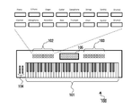
図1は、本発明による電子鍵盤楽器の一実施形態の外観図である。本実施形態は、電子鍵盤楽器100として実施される。電子鍵盤楽器100は、演奏操作子としての複数の鍵からなる鍵盤101と、音色選択操作子としての音色選択を行うための音色選択ボタン102及び音色以外の各種機能選択を行う機能選択ボタン103からなるスイッチ・パネルと、ピッチベンドやトレモロ、ビブラート等の各種モジュレーション(演奏効果)を付加するベンダ/モジュレーション・ホイール104、音色や音色以外の各種設定情報を表示するLCD(Liquid Crystal Display:液晶ディスプレイ)105等を備える。また、電子鍵盤楽器100は、特には図示しないが、演奏により生成された楽音を放音するスピーカを裏面部、側面部、又は背面部等に備える。
FIG. 1 is an external view of an embodiment of an electronic keyboard instrument according to the present invention. This embodiment is implemented as an
音色選択ボタン102は、図1に示されるように、ピアノ(図中「Piano」)、エレクトリックピアノ(図中「E.piano」)、オルガン(図中「Organ」)、ギター(図中「Guitar)等の各種音色のカテゴリを選択するためのボタン群である。ユーザは、この音色選択ボタン102を押下することにより、例えば16音色のうちの何れかを選択することができる。
As shown in FIG. 1, the tone
図2は、図1の電子鍵盤楽器100の実施形態のハードウェア例を示す図である。図2の電子鍵盤楽器100において、システム全体はバスコントローラ201によって制御される。バスコントローラ201はバス202上のデータの流れを司るものであるが、その役割は、バス202に接続されたデバイスの優先順位のコントロールである。例えば、メモリコントローラ203を介してバス202に接続されるRAM204は、CPU205と音源LSI206によって共有されているが、発音を行う音源LSI206はデータの欠落が許されないために優先度が最も高く設定されており、必要に応じてCPU205のアクセスを制限する。
FIG. 2 is a diagram showing a hardware example of the embodiment of the
バス202には、CPU205、音源LSI206、フラッシュメモリコントローラ207、メモリコントローラ203、DMA(ダイレクトメモリアクセス)コントローラ209、I/O(入出力)コントローラ210、I/Oコントローラ210を介して接続されるキー・スキャナ211とLCDコントローラ212とA/D(アナログ/デジタル)コンバータ213が接続される。
A key connected to the
CPU205は、電子鍵盤楽器100の全体の制御処理を実行する第1プロセッサである。音源LSI206は、楽音発音専用の大規模集積回路である第2プロセッサである。
The
フラッシュメモリコントローラ207は、大容量フラッシュメモリ208とバス202を接続するインタフェース回路である。大容量フラッシュメモリ208は、波形データ、制御プログラム、固定データ等格納する。
The
メモリコントローラ203は、RAM204とバス202を接続するインタフェース回路である。RAM204は、波形データ、制御プログラム、データを必要に応じて配置する。RAM204はまた、CPU205や音源LSI206に内蔵されるDSP(デジタルシグナルプロセッサ)のワーク領域としても使用される。
The
I/Oコントローラ210は、バス202と、図1の鍵盤101、音色選択ボタン102、機能選択ボタン103、ベンダ/モジュレーション・ホイール104、又はLCD105等の周辺デバイスとを接続するインターフェース回路である。I/Oコントローラ210に接続されるキー・スキャナ211は、図1の鍵盤101や音色選択ボタン102又は機能選択ボタン103等のスイッチ・パネルの状態を走査して、その走査結果をI/Oコントローラ210及びバス202を介してCPU205に通知する。I/Oコントローラ210に接続されるLCDコントローラ212は、図1のLCD105のデバイスをコントロールする。A/Dコンバータ213は、図1のベンダ/モジュレーション・ホイール104の走査位置を検出する。
The I /
DMAコントローラ209は、大容量フラッシュメモリ208とRAM204間のDMA転送を制御する。
The
図3は、音源LSI206を示すブロック図である。音源LSI206は、波形発生器301、バスインタフェース302、DSP303、及びミキサ304を含む。波形発生器301は、図2のRAM204から波形データ読み出して楽音波形として発生する#1から#256までの256組の発振器である波形読出し装置305を具備する。バスインタフェース302は、バス202と、波形発生器301、DSP303、及びミキサ304との接続を行うバスインタフェース回路であり、これら各部と図2のCPU205又はRAM204との通信を司る。DSP303は、楽音信号に音響効果をもたらすデジタル信号処理回路である。ミキサ304は、波形発生器301が出力する楽音信号を混合したり、DSP303に送ったり、DSP303からの音響信号を受け取ったりすることで全体の楽音信号の流れを制御し、外部に出力する。ミキサ304からのデジタル楽音信号は、図2のD/Aコンバータ214でアナログ楽音信号に変換される。このアナログ楽音信号は、アンプ215で増幅された後に、アナログ楽音出力信号として出力される。
FIG. 3 is a block diagram showing the
次に、図2の大容量フラッシュメモリ208は、NAND型フラッシュメモリなどの、大容量で安価なメモリデバイスである。なお、この大容量フラッシュメモリ208の代わりに、ハードディスク記憶装置や、ネットワーク上又はクラウド上のディスク装置が使用されてもよい。大容量フラッシュメモリ208には、主に以下のようなデータが格納されている。
・全ての音色の波形データ
・全ての音色のパラメータデータ
・CPU205やDSP303が実行するプログラム、プログラムの使用データ
・音楽データ
・ユーザの設定データ
波形データは例えば、1ワード長が16ビットのリニアPCMフォーマットデータである。
Next, the large-
-Waveform data of all tones-Parameter data of all tones-Programs executed by CPU205 and DSP303, data used by programs-Music data-User setting data Waveform data is, for example, a linear PCM format with a word length of 16 bits. It is data.
前述した大容量フラッシュメモリ208の内容は、CPU205からは任意のアドレスへのアクセスが可能であるが、音源LSI206からはアクセスすることができないので、大容量フラッシュメモリ208中の波形データをRAM204に転送する必要がある。しかしながら、RAM204の記憶容量は大容量フラッシュメモリ208よりも小さいために、全てデータをRAM204中の発音チャネル毎のバッファ領域に転送することはできない。従って、RAM204の記憶内容は必要に応じて逐次入れ替える必要がある。入替えが必要なデータの中で特に本実施形態が対象とするものは波形データであるが、波形データの制御の詳細については後述する。
The contents of the large-
図1から図3の本実施形態の動作の概要について、以下に説明する。まず本実施例では、演奏者が図1の音色選択ボタン102を押下することで図1に示される16音色のうちのいずれかを選択することができる。各音色は、それぞれ1音色当たり最大32種類の波形から構成され、波形データは大容量フラッシュメモリ208に格納されている。1音色の音域(キー番号)とベロシティ域が2次元的に分割され、それぞれのスプリット(分割)エリアに、上述の最大32個の波形が割り当てられている。即ち、押鍵時の速さ(ベロシティ)とキー番号(鍵盤101の番号)の2つのファクタから、読み出されるべき波形が1つだけ決定される、という制御が実施される。
The outline of the operation of the present embodiment of FIGS. 1 to 3 will be described below. First, in this embodiment, the performer can select one of the 16 tones shown in FIG. 1 by pressing the tone
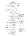
本実施例の音源LSI206は、波形読出しの際にループ処理を実行することが可能である。図4は、波形読出しループの動作の説明図である。以下の3つのアドレス情報に基づいてループ処理の制御が実行される。
The
1.波形バッファスタートアドレス:音源LSI206が読出しを開始する
ためのアドレス
2.波形バッファエンドアドレス:音源LSI206が読出しを行う最も
後方のアドレス
3.波形バッファループアドレス:波形バッファスタートアドレスと波形
バッファエンドアドレスの間に存在し、波形読出しが波形バッファ
エンドアドレスに達した場合に、次に読み出されるのがこの波形
バッファループアドレスである。
1. 1. Waveform buffer start address: Address for the
図4に示されるように、波形バッファは、波形バッファスタートアドレスから波形バッファループアドレスの直前までの、リングバッファとして機能させない非ループ区間(第1領域)と、波形バッファループアドレスから波形バッファエンドアドレスまでの、リングバッファとして機能させるループ区間(第2領域)とからなる。波形バッファに記憶されている波形バッファスタートアドレスから波形バッファエンドアドレスまでの波形データが読み出されるときに、波形バッファループアドレスから波形バッファエンドアドレスまでのループ区間で、繰り返し読出し動作が実行される。なお、波形バッファループアドレスが、波形バッファエンドアドレスと等しい場合は、ループ処理は行われず、読出しポインタが波形バッファエンドアドレスに達した時点で発音が停止する。 As shown in FIG. 4, the waveform buffer includes a non-loop section (first region) from the waveform buffer start address to immediately before the waveform buffer loop address, which does not function as a ring buffer, and a waveform buffer loop address to the waveform buffer end address. It consists of a loop section (second area) that functions as a ring buffer up to. When the waveform data from the waveform buffer start address to the waveform buffer end address stored in the waveform buffer is read out, the read-out operation is repeatedly executed in the loop section from the waveform buffer loop address to the waveform buffer end address. If the waveform buffer loop address is equal to the waveform buffer end address, loop processing is not performed and sounding stops when the read pointer reaches the waveform buffer end address.
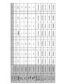
図5は、「フラッシュメモリ音色波形ディレクトリ」のデータ例を示す図である。フラッシュメモリ音色波形ディレクトリは、大容量フラッシュメモリ208上に格納されている全ての波形データの情報をまとめたテーブルである。具体的には、このテーブルは、「音色番号」及び「音色内波形番号」で決まる各音色の各波形それぞれが用いられる鍵域を示す「最低キー番号」と「最高キー番号」、前記各波形それぞれが用いられるベロシティ域情報である「最低ベロシティ」と「最高ベロシティ」、実際に大容量フラッシュメモリ208のどのアドレスに配置されているかを示す「波形領域先頭からのアドレス」、波形の長さを示す「波形サイズ」、読出しに使用される「スタートアドレス」、「ループアドレス」、及び「エンドアドレス」の情報をまとめたテーブルである。このテーブルは、電源投入時に、RAM204上に展開される。
FIG. 5 is a diagram showing a data example of the “flash memory tone waveform directory”. The flash memory tone waveform directory is a table that summarizes information on all waveform data stored in the large-
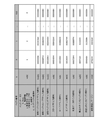
図6は、「RAM波形バッファディレクトリ」のデータ例を示す図である。RAM波形バッファディレクトリは、RAM204の波形バッファ上に格納されている波形データの情報をまとめたテーブルである。このテーブル上のバッファ番号bによって決まるバッファディレクトリの1つが持つ情報は、波形バッファbの使用状態を表す「バッファステータスvs[b]」、波形バッファb自体のスタート位置、ループ位置を表す、エンド位置をそれぞれ表す「波形バッファスタートアドレスbsa[b]」、「波形バッファループアドレスbla[b]」、及び「波形バッファエンドアドレスbea[b]」、波形バッファbに対応する転送元の大容量フラッシュメモリ208の音色波形領域のスタート位置、ループ位置を表す、エンド位置をそれぞれ表す「スタートアドレスsa[b]」、「ループアドレスla[b]」、及び「エンドアドレスea[b]」、CPU205による大容量フラッシュメモリ208上の現在の転送波形の読出しアドレスである「転送データポインタ」、CPU205によるRAM204への転送書込みアドレスである「書込みポインタ」、音源LSI206によるRAM204上の現在の読出しアドレスである「読出しポインタ」、そして、書込みポインタと読出しポインタ最新値との差分である「波形読出しマージン」が保持される。
FIG. 6 is a diagram showing a data example of the “RAM waveform buffer directory”. The RAM waveform buffer directory is a table that summarizes information on waveform data stored in the waveform buffer of
図6の例において、テーブルのバッファ情報の数は256用意されている。これは実際にRAM204上の波形バッファが常に256個に分割されているということではなく、初期状態では連続した転送可能領域を示すバッファ情報が1つ存在するだけであり、このバッファのバッファステータスvs[b]は1である。そのバッファのバッファスタートアドレスとバッファエンドアドレスはバッファ領域の全ての先頭と最後尾を保持する。これ以外のバッファの情報のバッファステータスは、具体的なRAM空間(RAM204のアドレス空間)を指し示していないためNULL値を持つ。
In the example of FIG. 6, 256 numbers of buffer information in the table are prepared. This does not mean that the waveform buffer on the
図7は、大容量フラッシュメモリ208上の音色波形領域からRAM204上の波形バッファへの音色波形転送動作の説明図である。まず、演奏されると、転送されるべき波形の番号が調べられる。まず、その番号の波形が使用中か転送可能状態かに関わらず、所望の波形がRAM204上に残っているかどうかが調べられる。もし存在すれば、波形転送は行われず、残っている波形がキャッシュ波形として流用される。
FIG. 7 is an explanatory diagram of a tone waveform transfer operation from the tone waveform area on the large-
キャッシュ波形が無ければ次に、波形サイズより大きい空き領域があるか否かが検索され、見つかればその転送可能領域が波形バッファとされて、波形転送が開始される。ここで、もし1つの転送可能領域のサイズが十分であればそれが使用される。サイズが十分な転送可能領域が見つからない場合、2つ以上の連続した転送可能領域が探索され、その合計サイズが十分であればそれが使用される。その場合には、波形バッファのディレクトリ情報が1つに集約され、空いたディレクトリ情報のステータスがNULLとされる。 If there is no cache waveform, then it is searched whether there is a free area larger than the waveform size, and if it is found, the transferable area is used as a waveform buffer, and waveform transfer is started. Here, if the size of one transferable area is sufficient, it is used. If no transferable area of sufficient size is found, two or more contiguous transferable areas are searched and used if the total size is sufficient. In that case, the directory information of the waveform buffer is aggregated into one, and the status of the vacant directory information is set to NULL.
それでも見つからない場合は、本実施例ではリングバッファの必要容量である16KBの空き領域が探索され、見つかった領域がリングバッファ方式で使用されることで発音が行われる。リングバッファ方式では、波形バッファがリングとして扱われることで、見かけ上無限のメモリ空間を確保する手法である。この場合、CPU205による書込みポインタのアドレス値が音源LSI206による読出しポインタのアドレス値を追い抜くことも追いつかれることも無いように、制御が実施される。このリングバッファ領域すらみつからない場合は、発音が断念される。
If it is still not found, in this embodiment, a free area of 16 KB, which is the required capacity of the ring buffer, is searched, and the found area is used in the ring buffer method to perform pronunciation. The ring buffer method is a method of securing an apparently infinite memory space by treating the waveform buffer as a ring. In this case, control is performed so that the address value of the write pointer by the
ところで、波形バッファvの書込みポインタwp[v]が音源LSI206の読出しポインタrp[v]を追い越せば、音源LSI206が読み出す波形データは、突然、不連続に過去のデータに戻ってしまい、ノイズが発生することになる。これは音楽的に許容できるものではない。
By the way, if the write pointer wp [v] of the waveform buffer v overtakes the read pointer rp [v] of the
そこで、本実施例では、波形バッファvにおける読出しポインタrp[v]が、波形データを充当しない状態でどれだけ読めるかというデータのワード数(アドレス)、即ち、書込みポインタwp[v]の値と読出しポインタrp[v]の値の差分が、波形読出しマージンとして管理される。本実施形態では、この波形読出しマージンが所定の値以下に達した場合、その楽音を発生しているボイスチャネルに対してダンプ処理(緩やかな消音処理)が実行され、その処理の後に発音が停止した時点でそのボイスチャネルの波形バッファvからの読出しが中止されることにより、ノイズの発生を防止することができる。 Therefore, in this embodiment, the read pointer rp [v] in the waveform buffer v is the number of words (address) of the data indicating how much the read pointer rp [v] can be read without allocating the waveform data, that is, the value of the write pointer wp [v]. The difference between the values of the read pointer rp [v] is managed as the waveform read margin. In the present embodiment, when the waveform read margin reaches a predetermined value or less, a dump process (gentle muffling process) is executed for the voice channel generating the musical tone, and the sound is stopped after the process. At that point, the reading from the waveform buffer v of the voice channel is stopped, so that the generation of noise can be prevented.
本実施例では、その波形読出しマージンの値は、固定値ではなく再生ピッチが考慮されて、原音ピッチによる再生時には1Kワード未満、1オクターブ上のピッチでの再生時には2Kワード未満、1オクターブ下のピッチでの再生時には512ワード未満になったら、ダンプ処理の実行が決定される。 In this embodiment, the value of the waveform read margin is less than 1 K word when reproduced at the original pitch, less than 2 K words when reproduced at a pitch one octave higher, and one octave lower, considering the reproduction pitch rather than a fixed value. When the number of words is less than 512 during playback on the pitch, the execution of the dump process is determined.
ダンプ処理の速度は、このまま波形が補充されずに読み進んだとしても、すでに波形バッファvに転送された読込みマージン分の波形データが読み切られる前に消音できるだけの速度であればよい。その速度は現在の再生ピッチに依存する。 The speed of the dump processing may be such that even if the waveform is read without being replenished as it is, the waveform data for the read margin already transferred to the waveform buffer v can be muted before it is completely read. Its speed depends on the current playback pitch.
図8は、図2のCPU205が実行する制御処理のメインルーチンの処理例を示すフローチャートである。図1の電子鍵盤楽器100において、機能選択ボタン103により装置電源がパワーオンされると、CPU205は、図8のフローチャートで示されるメインルーチンを起動し、まず装置各部を初期化する初期化処理を実行する(ステップS901)。ステップS801の初期化処理が完了すると、ユーザが図1の音色選択ボタン102又は機能選択ボタン103の操作状態を取り込むスイッチ処理(ステップS802)、ステップS802の処理の結果に基づく音色選択ボタン102が操作された際の音色選択イベントの検出及び音色選択処理(ステップS803→S804)、ユーザが図1の鍵盤101を弾いた際の押鍵イベントや離鍵イベントを取り込む鍵盤処理(ステップS805)、ステップS805の処理の結果に基づく押鍵イベントの検出及び押鍵処理(ステップS806→S807)、ステップS805の処理の結果に基づく離鍵イベントの検出及び離鍵処理(ステップS808→S809)、及び音源LSI206からのイベントの処理を行う音源イベント処理(ステップS810)が、繰り返し実行される。
FIG. 8 is a flowchart showing a processing example of the main routine of the control processing executed by the
図9(a)は、図8のステップS801の初期化処理の詳細例を示すフローチャートである。まず、CPU205は、大容量フラッシュメモリ208からフラッシュメモリ音色波形ディレクトリ(図5参照)のテーブルデータを、RAM204上の指定されたアドレスに転送する(ステップS901)。
FIG. 9A is a flowchart showing a detailed example of the initialization process of step S801 of FIG. First, the
次に、ステップS902とステップS905の繰返し制御処理によりバッファ情報数(=256)分のループ処理が実行される。このループ処理中のステップS903において、バッファ番号b(図6のRAM波形バッファディレクトリを参照)の値が判定される。 Next, the loop processing for the number of buffer information (= 256) is executed by the iterative control processing of step S902 and step S905. In step S903 during this loop processing, the value of the buffer number b (see the RAM waveform buffer directory in FIG. 6) is determined.
CPU205は、バッファ番号b=0のときは、RAM204に記憶される図6に例示されるRAM波形バッファディレクトリを初期化した後に、そのディレクトリ内のバッファ番号b=0に対応するバッファステータスを転送可能(=1)に設定する(ステップS903→S904)。その後、CPU205は、ループ処理を続行する(ステップS904→S906)。
When the buffer number b = 0, the
一方、CPU205は、バッファ番号b≠0のときは、RAM波形バッファディレクトリを初期化した後に、そのディレクトリ内の上記バッファ番号bに対応するバッファステータスをNULL(=0)に設定する(ステップS903→S905)。その後、CPU205は、ループ処理を続行する(ステップS905→S906)。
On the other hand, when the buffer number b ≠ 0, the
上記ステップS902からS906のループ処理が終了後、CPU205は、RAM204上の波形バッファのリンク情報を初期化する(ステップS907)。リンク情報とは、RAM204上の波形バッファ領域に対して、先頭から順番にどのRAM波形バッファが使用されているかのバッファ番号が取得できる情報である。初期化時は、波形領域が1つなので、リンク情報の先頭番号が0に設定される。
After the loop processing of steps S902 to S906 is completed, the
次に、CPU205は、RAM204上の波形バッファへのアクセスカウントを初期化する(ステップS908)。アクセスカウントとは、RAM波形バッファディレクトリ(図6参照)のバッファ番号bで指定される波形データに、波形読出し装置305(図3参照)がいくつアクセスしているかを示す情報である。
Next, the
次に、CPU205は、大容量フラッシュメモリ208の音色波形領域から波形バッファへの波形転送を管理するための、転送要求カウンタ、転送状態フラグ、転送要求バッファ(リンク構造)を初期化する(S909)。転送要求カウンタは、RAM204上の波形バッファに対して、RAM波形バッファディレクトリで示されるバッファのうち、波形データが転送中のバッファが現在いくつあるか管理するもので情報である。転送状態フラグは、音色波形領域から波形バッファへ波形データを転送中か否かを判断するフラグ情報である。転送要求バッファは、次にどの波形バッファに対して音色波形領域から波形バッファへの波形転送を行うかを管理するためのバッファである。その後、CPU205は、図9(a)のフローチャートで示される図8のステップS801の初期化処理を終了する。
Next, the
図9(b)は、図8のステップS804の音色選択処理の詳細例を示すフローチャートである。CPU205は、押鍵処理などで使用するために、図1の音色選択ボタン102の操作により指定された音色番号を、CPU205内のワークメモリ等に保存しておく(ステップS910)。
FIG. 9B is a flowchart showing a detailed example of the tone color selection process in step S804 of FIG. The
図10及び図11は、図8のステップS807の押鍵処理の詳細例を示すフローチャートである。CPU205は、鍵盤が弾かれた際の押鍵による演奏情報(鍵盤位置、押された強さ)を、キー番号、ベロシティに変換し、これらに基づく制御処理を実行する。
10 and 11 are flowcharts showing a detailed example of the key pressing process in step S807 of FIG. The
CPU205は、最初に、この押鍵での発音に、音源LSI206内のどの波形読出し装置305(図3)を使用するかを決定するボイスアサインを実行する(ステップS1001)。
The
次に、CPU205は、キー番号、ベロシティ、現在の音色番号から、音色波形領域から波形バッファへ転送を行うべき波形番号wを取得する(ステップS1002)。
Next, the
次に、CPU205は、キー番号、波形番号wから得られる波形情報から、再生ピッチを計算する(ステップS1003)。
Next, the
次に、CPU205は、再生ピッチから、波形読出しマージン(図6参照)を決定する(ステップS1004)。
Next, the
次に、CPU205は、押鍵情報から取得した波形番号の波形データが既にRAM204上の波形バッファに存在するかを確認するキャッシュ波形確認処理を実行する(ステップS1005)。この処理の詳細については、図13(d)を用いて後述する。
Next, the
ステップS1005でのキャッシュ波形確認処理の結果、既に波形データがRAM204上のいずれかの波形バッファに存在する場合は、CPU205は、その波形データをキャッシュ波形として使用して、音源LSI206内の波形読出し装置305(図3)による波形読出しを開始する(図10のステップS1005→図11のステップS1019)。その後、CPU205は、図10と図11のフローチャートで示される図8のステップS807の押鍵処理を終了する。
As a result of the cache waveform confirmation process in step S1005, if the waveform data already exists in any of the waveform buffers on the
ステップS1005でのキャッシュ波形確認処理の結果、キャッシュ波形データがRAM204上に存在しない場合は、CPU205は、次のようにして、波形データが転送可能な波形バッファの確認処理を行う。CPU205は、RAM204上の波形バッファのリンク情報から、RAM204上の波形バッファ領域に対する先頭のバッファ番号を取得する(ステップS1005→S1006)。
If the cache waveform data does not exist on the
次に、CPU205は、RAM204上の波形バッファに対するループ処理の際に、直前のバッファ番号に対するバッファステータスが転送可能であったことを示すフラグ(以後「フラグA」と記載)を0に初期化する(ステップS1007)。
Next, the
次に、CPU205は、ステップS1008とS1014のループ制御処理により、RAM波形バッファディレクトリ(図6)のバッファ情報数分、以下のステップS1009からS1013までの一連の処理を繰返し実行する。
Next, the
この一連の処理において、CPU205はまず、リンク情報から取得したバッファ番号bに対し、バッファステータス(図6)を判定する(ステップS1009)。
In this series of processes, the
CPU205は、バッファステータスの値がNULL(=0)、減衰中(=3)、又はリングバッファ使用中(=4)(図6参照)である場合は、フラグAを0に設定する(ステップS1010)。
The
続いて、CPU205は、RAM204上の波形バッファのリンク情報から、次に処理するバッファ番号を取得する(ステップS1011)。その後、CPU205は、繰返し処理を継続する(ステップS1011→S1014)。
Subsequently, the
CPU205は、バッファステータスの値が転送可能(=1)(図6参照)である場合は、バッファステータスが転送可能時の処理を実行する(ステップS1012)。この処理の詳細については、図12を用いて後述する。その後、CPU205は、繰返し処理を継続する(ステップS1012→S1014)。
When the value of the buffer status is transferable (= 1) (see FIG. 6), the
CPU205は、バッファステータスの値が発音中(=2又は3)(図6参照)である場合は、バッファステータスが発音中時の処理を実行する(ステップS1013)。この処理の詳細については、図13(c)を用いて後述する。その後、CPU205は、繰返し処理を継続する(ステップS1013→S1014)。
When the value of the buffer status is sounding (= 2 or 3) (see FIG. 6), the
CPU205は、上述のステップS1008からS1014の繰返し処理が終了した時点で、RAM波形バッファディレクトリ(図6)で示されるいずれかのバッファ番号がアサインされたか否かを判定する(図11のステップS1015)。
The
CPU205は、ステップS1015で何れかのバッファ番号bがアサインされたと判定した場合は、バッファ番号bに対応する波形バッファに対して、波形データが転送中か否かを判定する(図11のステップS1015→S1016)。
When the
CPU205は、ステップS1016で転送が完了していると判定した場合は、音源LSI206内の波形読出し装置305(図3)による波形読出しを開始する(ステップS1016→S1019)。その後、CPU205は、図10と図11のフローチャートで示される図8のステップS807の押鍵処理を終了する。
When the
CPU205は、ステップS1016で転送中であると判定した場合は、バッファ番号bに対応する書込みポインタwp[b]と読出しポインタrp[b]の差分からの波形読み出しマージンの計算(ステップS1017)と、現在の波形読み出しマージンが波形読み出し開始マージンの閾値より大きくなったか否かの判定(ステップS1018)を繰り返し実行する。やがてステップS1018で現在の波形読み出しマージンが波形読み出し開始マージンの閾値より大きくなったと判定されると、CPU205は、音源LSI206の波形読出し装置305(図3)による波形読出しを開始する(ステップS1018→S1019)。その後、CPU205は、図10と図11のフローチャートで示される図8のステップS807の押鍵処理を終了する。
When the
CPU205は、ステップS1015でどのバッファ番号もアサインされなかったと判定した場合は、CPU205内のワークメモリ等から、16KB以上の転送可能バッファがあるか否かを判定する(ステップS1015→S1020)。
When the
ステップS1020の判定がYESならば、CPU205は、リングバッファ方式での発音処理を実行する(ステップS1020→S1021)。その後、CPU205は、図10と図11のフローチャートで例示される図8のステップS807の押鍵処理を終了する。
If the determination in step S1020 is YES, the
ステップS1020の判定もNOならば、CPU205は、発音処理は断念して、図10と図11のフローチャートで例示される図8のステップS807の押鍵処理を終了する。
If the determination in step S1020 is also NO, the
図13(d)は、図10のステップS1005のキャッシュ波形確認処理の詳細例を示すフローチャートである。 FIG. 13D is a flowchart showing a detailed example of the cache waveform confirmation process in step S1005 of FIG.
CPU205はまず、ステップS1430とS1436の繰返し制御処理により、RAM波形バッファディレクトリ(図6)のバッファ情報数分、以下のステップS1431からS1435の一連の処理を、繰返し実行する。
First, the
上記一連の処理において、CPU205はまず、リンク情報から取得したバッファ番号bに対し、バッファステータス(図6)を判定する(ステップS1431)。
In the above series of processes, the
CPU205は、バッファステータスの値がNULL(=0)、減衰中(=3)、又はリングバッファ使用中(=4)(図6参照)である場合は、そのまま現在のバッファ番号bに対する処理を終了して、次のバッファ番号に対する処理に移行する(ステップS1431→S1436)。
When the value of the buffer status is NULL (= 0), decaying (= 3), or ring buffer is in use (= 4) (see FIG. 6), the
CPU205は、バッファステータスの値が転送可能(=1)、又は発音中(=2又は3)(図6参照)である場合は、押鍵情報から取得した波形番号の波形データとRAM波形バッファディレクトリで示される現在のバッファ番号bの波形バッファの波形データが同一であるか否かを判定する(ステップS1432)。
When the buffer status value is transferable (= 1) or sounding (= 2 or 3) (see FIG. 6), the
CPU205は、ステップS1432で、上記各波形データが異なると判定した場合は、そのまま現在のバッファ番号bに対する処理を終了して、次のバッファ番号に対する処理に移行する(ステップS1431→S1436)。
If the
CPU205は、ステップS1432で、上記各波形データが同一であると判定した場合は、バッファステータスを発音中に変更する(ステップS1433)。
When the
次に、CPU205は、RAM波形バッファへのアクセスカウントをインクリメントする(ステップS1434)。
Next, the
そして、CPU205は、現在のバッファ番号bにあるキャッシュ波形を使用するとして、図13(d)のフローチャートで例示される図10のステップS1005のキャッシュ波形確認処理を終了する。
Then, assuming that the cache waveform in the current buffer number b is used, the
ステップS1436で全ての繰返し処理が終了した場合には、CPU205は、キャッシュ波形無しとして、図13(d)のフローチャートで例示される図10のステップS1005のキャッシュ波形確認処理を終了する。
When all the iterative processing is completed in step S1436, the
図12は、図10のステップS1010のバッファステータスが転送可能時の処理の詳細例を示すフローチャートである。 FIG. 12 is a flowchart showing a detailed example of processing when the buffer status in step S1010 of FIG. 10 can be transferred.
まずCPU205は、現在のバッファ番号bの波形バッファのサイズbuf_szを取得する(ステップS1201)。buf_szは、RAM波形バッファディレクトリ内のバッファ番号bに対応する波形バッファエンドアドレスと波形バッファスタートアドレスの差として算出できる。
First, the
次に、CPU205は、上記buf_szを、押鍵情報から取得した波形番号wの波形データのサイズ(wave_sz[w])と比較する(ステップS1202)。wave_sz[w]は、図5のフラッシュメモリ音色波形ディレクトリ中の該当波形番号wに対応する波形サイズとして算出できる。
Next, the
CPU205は、ステップS1202で波形バッファのサイズbuf_szが押鍵に対応する波形データのサイズwave_sz[w]以上であると判定した場合、RAM波形バッファ分割処理を実行する。この処理の詳細については図13(a)を用いて後述する。
When the
CPU205は、ステップS1202で波形バッファのサイズbuf_szが押鍵に対応する波形データのサイズwave_sz[w]より小さいと判定した場合、フラグAの値を判定する(ステップS1209)。
When the
CPU205は、ステップS1209でフラグAの値が1であると判定した場合、CPU205のワークメモリに記憶してある連続した直前の波形バッファサイズpre_buf_sz(ステップS1213参照)と現在の波形バッファのサイズbuf_szとを加算した波形バッファサイズpre_buf_sz+buf_szと、波形データのサイズwave_sz[w]とを比較する(ステップS1210)。
When the
CPU205は、ステップS1210でpre_buf_sz+buf_szがwave_sz[w]以上であると判定した場合、RAM波形バッファ結合処理を実行する。この処理の詳細については図13(a)を用いて後述する。
When the
ステップS1203のRAM波形バッファ分割処理又はステップS1211のRAM波形バッファ結合処理の後、CPU205は、バッファ番号bのバッファに対する書込みポインタwp[b]と読出しポインタrp[b]を0に設定する(ステップS1204)。
After the RAM waveform buffer division processing in step S1203 or the RAM waveform buffer coupling processing in step S1211, the
次に、CPU205は、後述する波形転送管理処理に対して、新規転送要求イベントを発行する(ステップS1205)。
Next, the
その後、CPU205は、現在のバッファ番号bで示されるバッファのアドレス情報(図6参照)である波形バッファスタートアドレスbsa[b]、波形バッファループアドレスbla[b]、波形バッファエンドアドレスbea[b]、スタートアドレスsa[b]、ループアドレスla[b]、エンドアドレスea[b]を更新する(ステップS1206)。
After that, the
次に、CPU205は、現在のバッファ番号bで示される波形バッファの波形読出しマージン(図6参照)を更新する(ステップS1207)。
Next, the
更に、CPU205は、現在のバッファ番号bで示されるバッファステータス(図6参照)を発音中に変更する(ステップS1208)。
Further, the
そして、CPU205は、RAM204上の波形バッファへのアクセスカウントをインクリメントする(ステップS1212)。その後、CPU205は、図12のフローチャートで例示される図10のステップS1012のバッファステータスが転送可能時の処理を終了すると共に、図10のステップS1008からS1014のループ処理を抜ける。
Then, the
CPU205は、ステップS1209でフラグAの値が0であると判定した場合、又はステップS1210でre_buf_sz+buf_szがwave_sz[w]より小さいと判定した場合には、ステップS1213からS1217の一連の処理を実行する。
When it is determined in step S1209 that the value of flag A is 0, or when it is determined in step S1210 that re_buf_sz + buf_sz is smaller than wave_sz [w], the
この一連の処理において、CPU205はまず、次のループ処理で使用できるよう現在の波形バッファのサイズbuf_szを、CPU205内のワークメモリ等にpre_buf_szとして保存しておく(ステップS1213)。
In this series of processing, the
次に、CPU205は、波形バッファサイズbuf_szを判定する(ステップS1214)。
Next, the
CPU205は、ステップS1214でbuf_szが16KB以上と判定した場合、バッファ番号bをCPU205内のワークメモリ等に保存しておく(ステップS1215)。CPU205は、ステップS1214でbuf_szが16KBより小さいと判定した場合は、上記ステップS1215の処理はスキップする。
When the
その後、CPU205は、フラグAの値を1に設定する(ステップS1216)。
After that, the
更に、CPU205は、RAM波形バッファのリンク情報から、次に処理するバッファ番号を取得する(ステップS1217)。その後、CPU205は、図12のフローチャートで例示される図10のステップS1012のバッファステータスが転送可能時の処理を終了し、図10のステップS1008からS1014の繰返し処理を継続する。
Further, the
図13(a)は、図12のステップS1203のRAM波形バッファ分割処理の詳細例を示すフローチャートである。 FIG. 13A is a flowchart showing a detailed example of the RAM waveform buffer division processing in step S1203 of FIG.
まずCPU101は、バッファサイズbuf_szを、押鍵情報から取得した波形番号wの波形データのサイズ(wave_sz[w])と比較する(ステップS1301)。
First, the
CPU205は、ステップS1301で波形バッファのサイズbuf_szが押鍵に対応する波形データのサイズwave_sz[w]以下であると判定した場合、そのまま図13のフローチャートで例示される図12のステップS1203のRAM波形バッファ分割処理を終了する。
When the
CPU205は、ステップS1301で波形バッファのサイズbuf_szが押鍵に対応する波形データのサイズwave_sz[w]より大きいと判定した場合、波形データ分を使用し、残りを転送可能とする波形バッファの分割を行う。まずCPU101は、現在のバッファ番号の波形バッファのサイズを波形データと同じサイズに設定する(ステップS1302)。
When the
次にCPU101は、RAM波形バッファのリンク情報から、バッファステータスがNULLであるバッファのバッファ番号を取得する。次に、CPU101は、前述のバッファサイズbuf_szから波形データのサイズwave_sz[w]を差し引いた残りのサイズを設定し、バッファステータスを転送可能に設定する(以上、ステップS1303)。
Next, the
最後に、CPU101は、RAM波形バッファのリンク情報に対して、バッファステータスを転送可能としたバッファが現在のバッファの直後になるよう更新を行う(ステップS1304)。その後、CPU101は、図13(a)のフローチャートで示される図12のステップS1203のRAM波形バッファ分割処理を終了する。
Finally, the
図13(b)は、図12のステップS1211のRAM波形バッファ結合処理の詳細例を示すフローチャートである。 FIG. 13B is a flowchart showing a detailed example of the RAM waveform buffer coupling process in step S1211 of FIG.
まずCPU101は、直前のバッファ番号に対するバッファステータスをNULLに変更する(ステップS1310)。
First, the
そして、CPU205は、RAM波形バッファのリンク情報に対して、直前のバッファ番号と現在のバッファ番号に対して直前のバッファ番号が最後尾になるよう
更新を行う(ステップS1311)。その後、CPU101は、図13(b)のフローチャートで示される図12のステップS1211のRAM波形バッファ結合処理を終了する。
Then, the
図13(c)は、図10のステップS1013のバッファステータスが発音中の処理の詳細例を示すフローチャートである。 FIG. 13 (c) is a flowchart showing a detailed example of the process in which the buffer status of step S1013 in FIG. 10 is sounding.
CPU205はまず、フラグAを0に設定する(ステップS1320)。
First, the
そして、CPU205は、RAM波形バッファのリンク情報から、次に処理するバッファ番号を取得する(ステップS1321)。その後に、CPU205は、図13(c)のフローチャートで例示される図10のステップS1013のバッファステータスが発音中の処理を終了し、図10のステップS1008からS1014の繰返し処理を継続する。
Then, the
図14及び図15は、波形転送管理処理を示すフローチャートである。CPU205は、図14のステップS1401、S1402、及びS1403でそれぞれ、波形転送管理処理に対して発行されたイベントが、新規転送要求、転送要求、転送終了、又は転送停止の何れであるかを判定し、それぞれのイベントに対応した処理を実行する。
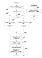
14 and 15 are flowcharts showing waveform transfer management processing. The
新規転送要求イベントが発行された場合(図12のステップS1205参照)、図14のステップS1401の判定がYESとなって、図15のステップS1416の処理が実行される。ステップS1416で、CPU205は、転送状態フラグを確認する。
When a new transfer request event is issued (see step S1205 in FIG. 12), the determination in step S1401 in FIG. 14 becomes YES, and the process in step S1416 in FIG. 15 is executed. In step S1416, the
ステップS1416で転送状態フラグが転送終了待ちであると判定した場合は、別のバッファに対して音色波形領域から波形バッファへの波形転送を行っている最中であるので、CPU205は、別のバッファの転送終了イベントからの転送要求イベントで処理されるように、転送要求バッファの先頭に該当バッファを設定する(図15のステップS1425)。その後、CPU205は、図14及び図15のフローチャートで示される波形転送管理処理を終了する。
If it is determined in step S1416 that the transfer status flag is waiting for the end of transfer, the
ステップS1416で転送状態フラグが待機状態であると判定した場合は、CPU205はまず、該当バッファ番号に対して、転送1回あたりの読出しサイズ(ここでは2ページ)を指定し、後述する波形読出し、波形バッファ転送処理(図16)に、転送要求を発行する(図15のステップS1417)。
When it is determined in step S1416 that the transfer status flag is in the standby state, the
次に、CPU205は、転送状態フラグを転送終了待ちに設定し(図15のステップS1418)、該当バッファを転送要求バッファの最後尾に設定する(図15のステップS1419)。
Next, the
次に、CPU205は、転送データポインタtp[v]を更新し(図15のステップS1420)、転送要求バッファカウンタをインクリメントする(図15のステップS1421)。
Next, the
次に、CPU205は、バッファステータスを判定する(図15のステップS1422)。バッファステータスが発信中と判定した場合は、波形バッファ内に波形の全てが転送可能であるので、全データが転送完了したかを判定する(図15のステップS1423)。この判定は、転送データポインタがエンドアドレスに到達したかどうかで判断できる。
Next, the
全データの転送が完了している場合は、これ以上の転送は必要ないので、波形転送管理処理に対して、転送停止イベントを発行する(図15のステップS1424)。その後、CPU205は、図14及び図15のフローチャートで示される波形転送管理処理を終了する。
When the transfer of all the data is completed, no further transfer is required, so a transfer stop event is issued to the waveform transfer management process (step S1424 in FIG. 15). After that, the
ステップS1422で、バッファステータスが発信中以外と判定した場合、或いは、ステップS1423で全データの転送が完了していないと判定した馬合には、CPU205は、図14及び図15のフローチャートで示される波形転送管理処理を終了する。
If it is determined in step S1422 that the buffer status is other than being transmitted, or if it is determined in step S1423 that the transfer of all data has not been completed, the
後述する波形読出し、波形バッファ転送処理で指定サイズ分の波形データの転送が終了し波形転送管理処理に対して転送終了の要求イベントが発行された場合(図16のステップS1607)、図14のステップS1401及びS1402の判定がNO、ステップS1403の判定がYESとなって、図14のステップS1406の処理が実行される。ステップS1406で、CPU205は、転送要求バッファに転送待ちのバッファがあるか否か、即ち、転送要求バッファカウンタが0でないか0であるかを判定する。
When the transfer of waveform data of a specified size is completed in the waveform read and waveform buffer transfer processes described later and a transfer end request event is issued to the waveform transfer management process (step S1607 of FIG. 16), the step of FIG. The determination of S1401 and S1402 is NO, the determination of step S1403 is YES, and the process of step S1406 of FIG. 14 is executed. In step S1406, the
ステップS1406の判定がNOならば、音色波形領域から波形バッファへの全ての転送が終了した状態なので、CPU205はそのまま何もせずに、図14及び図15のフローチャートで例示される現在の波形転送管理処理を終了する。
If the determination in step S1406 is NO, all the transfers from the tone waveform region to the waveform buffer have been completed. Therefore, the
ステップS1406の判定がYESならば、CPU205は、次のバッファが処理されるよう波形転送管理処理に対して、転送要求イベントを発行し(ステップS1407)、図14及び図15のフローチャートで例示される現在の波形転送管理処理を終了する。
If the determination in step S1406 is YES, the
上述した図14のステップS1407の処理により、波形転送管理処理に対して転送要求イベントが発行されると、図14のステップS1401の判定がNO、ステップS1402の判定がYESとなって、図14のステップS1408の処理が実行される。ステップS1408で、CPU205は、転送要求バッファの先頭のバッファについて転送処理を実行する。書込みポインタwp[v]と読出しポインタrp[v]を確認し、波形バッファvへの転送を行うことによって、書込みポインタwp[v]が読出しポインタrp[v]を追い越してしまう場合は、そのバッファvについては、転送要求バッファの最後尾に設定し、先頭から2番目のバッファに対して処理を行う。
When a transfer request event is issued to the waveform transfer management process by the process of step S1407 of FIG. 14, the determination of step S1401 of FIG. 14 is NO, the determination of step S1402 is YES, and FIG. The process of step S1408 is executed. In step S1408, the
次に、CPU205は、該当バッファ番号に対して、転送1回あたりの読出しサイズ(こでは2ページ)を指定し、後述する波形読出し、波形バッファ転送処理(図16)に、転送要求を発行する(図14のステップS1409)。
Next, the
次に、CPU205は、転送状態フラグを転送終了待ちに設定し(図14のステップS1410)、該当バッファを転送要求バッファの最後尾に設定する(図14のステップS1411)。
Next, the
次に、CPU205は、転送データポインタtp[v]を更新する(図14のステップS1412)。
Next, the
次に、CPU205は、バッファステータスを判定する(図14のステップS1413)。バッファステータスが発信中と判定した場合は、波形バッファ内に波形の全データが転送完了したかを判定する(図14のステップS1414)。この判定は、転送データポインタがエンドアドレスに到達したかどうかで判断できる。
Next, the
全データの転送が完了している場合は、これ以上の転送は必要ないので、波形転送管理処理に対して、転送停止イベントを発行する(図14のステップS1415)。その後、CPU205は、図14及び図15のフローチャートで示される波形転送管理処理を終了する。
When the transfer of all data is completed, no further transfer is required, so a transfer stop event is issued to the waveform transfer management process (step S1415 in FIG. 14). After that, the
ステップS1413で、バッファステータスが発信中以外と判定した場合、或いは、ステップS1414で全データの転送が完了していないと判定した場合には、CPU205は、図14及び図15のフローチャートで示される波形転送管理処理を終了する。
If it is determined in step S1413 that the buffer status is other than being transmitted, or if it is determined in step S1414 that the transfer of all data has not been completed, the
図15のステップS1424、図14のステップS1415、又は後述する音源イベント処理(図17のステップS1708)において波形転送管理処理に対して転送停止イベントが発行された場合、図14のステップS1401、S1402、及びS1403の判定が何れもNOとなって、ステップS1404が実行される。この場合、CPU205は、転送要求バッファから該当バッファを削除し(ステップS1404)、転送要求バッファカウンタをデクリメントする(ステップS1405)。その後、CPU205は、図14及び図15のフローチャートで示される波形転送管理処理を終了する。
When a transfer stop event is issued for the waveform transfer management process in step S1424 of FIG. 15, step S1415 of FIG. 14, or the sound source event process (step S1708 of FIG. 17) described later, steps S1401 and S1402 of FIG. 14 And S1403 are all NO, and step S1404 is executed. In this case, the
図16は、波形読出し、波形バッファ転送処理を示すフローチャートである。このフローチャートの処理は、図15のステップS1417又は図14のステップS1409からの転送要求イベントにより起動される。 FIG. 16 is a flowchart showing waveform reading and waveform buffer transfer processing. The processing of this flowchart is activated by the transfer request event from step S1417 of FIG. 15 or step S1409 of FIG.
CPU205は、ステップS1601とS1605のループ制御処理により、以下のステップS1602からS1604の一連の処理を、波形転送管理処理(図15のステップS1417又は図14のステップS1409)で指定された指定サイズ分繰り返し実行する。
The
まず、ステップS1602で、CPU205は、転送データポインタtp[v]に基づいて、大容量フラッシュメモリ208の音色波形領域wからページ単位で波形データを読み込む。
First, in step S1602, the
次に、ステップS1603で、CPU205は、波形バッファループアドレス及び波形バッファエンドアドレスを考慮し、ループ読出しの場合は、不要な部分は読み捨てる。
Next, in step S1603, the
そして、ステップS1604で、CPU205は、波形バッファvの書込みポインタwp[v]に応じたアドレスに、ステップS1602及びS1603で音色波形領域wから読み出した波形データの書込みを行う。CPU205は、書き込んだサイズ分、書込みポインタwp[v]を更新する。
Then, in step S1604, the
上記ステップS1601からS1605の繰返し処理が終了すると、CPU205は、転送状態フラグに待機状態を設定し(ステップS1606)、前述した波形転送管理処理に対して、転送終了イベントを発行する(ステップS1607)。その後、CPU205は、図16のフローチャートで示される波形読出し、波形バッファ転送処理を終了する。
When the iterative processing of steps S1601 to S1605 is completed, the
図17は、図8のステップS810の音源イベント処理の詳細例を示すフローチャートである。CPU205は、図8のステップS809の離鍵処理によってリリース状態に移行したバッファが、リリースレベルに到達したか否かを判定する(ステップS1701)。
FIG. 17 is a flowchart showing a detailed example of the sound source event processing in step S810 of FIG. The
CPU205は、ステップS1701の判定において、リリースレベルへの到達を判定しなかった場合は、そのまま図17のフローチャートで示される図8のステップS810の音源イベント処理を終了する。
If the
CPU205は、ステップS1701の判定において、リリースレベルへの到達を判定した場合は、その判定に対応する音源LSI206内の波形読出し装置305(図3)に対して、波形読出しの停止(発音終了)を指示する(ステップS1702)。
When the
次に、CPU205は、RAM上の波形バッファへのアクセスカウントをデクリメントする(ステップS1703)。
Next, the
CPU205は、ステップS1703でのデクリメント処理後のアクセスカウントの値を判定する(ステップS1704)。
The
CPU205は、ステップS1704の判定でアクセスカウントの値が0であると判定した場合は、対応する波形バッファのバッファステータスを転送可能に設定する(ステップS1705)。
When the
CPU205は、ステップS1704の判定でアクセスカウントの値が0ではないと判定した場合は、ステップS1705の処理はスキップする。
If the
次に、CPU205は、バッファステータスを判定する(ステップS1706)。
Next, the
CPU205は、ステップS1706の判定で、リングバッファが使用中でないと判定した場合には、更に全データの転送が完了しているか否かを判定する(ステップS1707)。
If the determination in step S1706 determines that the ring buffer is not in use, the
CPU205は、ステップS1706の判定でリングバッファが使用中であると判定した場合、又はステップS1707の判定が全データの転送が完了していないと判定した場合には、前述した波形転送管理処理に対して転送停止イベントを発行する(ステップS1708)。その後、CPU205は、図17のフローチャートで例示される図8のステップS810の音源イベント処理を終了する。
When the
CPU205は、ステップS1707の判定が全データの転送が完了していると判定した場合には、そのまま図17のフローチャートで例示される図8のステップS810の音源イベント処理を終了する。
When the determination in step S1707 determines that the transfer of all data has been completed, the
以上説明したようにして、本発明の一実施形態では、音源LSI206が読み出す波形データが格納される高速小容量のRAM204と、機器全ての音色波形データを保持するNANDフラッシュなどの低速大容量フラッシュメモリ208とを有し、演奏時に大容量フラッシュメモリ208内の音色波形領域からRAM204内の波形バッファに転送を開始し、所定容量転送後に音源が読み出しを開始する逐次転送型楽音発生装置において、波形バッファの領域を等分割して固定サイズを割り当てるのではなく、1つの連続領域をダイナミックに分割使用して1回の読み出しで1つの波形の全てのデータをバッファに転送して発音を行うことで波形ループ区間の転送を1回で済ませてトータルの波形転送負荷を軽減することが可能となる。また、本実施形態では、新たな発音に必要な波形が波形バッファ上に残っているならば、キャッシュ波形として再利用することが可能となる。更に、本実施形態では、波データ形を読み出すだけの波形バッファが確保できない場合は、余っている領域をリングバッファとして使用することで従来通りのループ読み出しを行うことが可能となる。これらの制御により、本実施形態では、同時発音数を改善することができる楽音発生装置、又はそのような楽音発生装置を用いた電子楽器を実現できる。あるいは性能低下を改善するためのハードウェアのコストを削減できる楽音発生装置、又はそのような楽音発生装置を用いた電子楽器を実現することが可能となる。
As described above, in one embodiment of the present invention, a high-speed small-
以上説明した実施形態の動作に加えて、次のような制御動作が実施されてもよい。上述の実施形態において、リングバッファとして使用できる領域(第2領域)も確保できない場合には、発音を断念するのではなく、次のような処理が実行される。波形バッファ(第2記憶手段)内における複数の領域のうち、他の波形データが既に記憶されている領域を、波形データを転送可能な転送可能領域として確保する転送領域確保処理と転送領域確保処理により確保された転送可能領域に、波形データを転送する第3転送処理とが実行される。これにより、ほとんど発音が終了している波形データ又は発音音量が小さくなっている波形データを消音させて、新たな波形データの発音を開始させることが可能となり、発音断念の可能性をできる限り低くすることが可能となる。 In addition to the operation of the embodiment described above, the following control operation may be performed. In the above-described embodiment, when the area that can be used as the ring buffer (second area) cannot be secured, the following processing is executed instead of giving up the sounding. Transfer area securing process and transfer area securing process for securing an area in which other waveform data is already stored as a transferable area in which waveform data can be transferred among a plurality of areas in the waveform buffer (second storage means). A third transfer process for transferring waveform data to the transferable area secured by the above is executed. As a result, it is possible to mute the waveform data whose pronunciation is almost finished or the waveform data whose pronunciation volume is low and start the pronunciation of new waveform data, and the possibility of abandoning the pronunciation is as low as possible. It becomes possible to do.
その他、本発明は上述した実施形態に限定されるものではなく、実施段階ではその要旨を逸脱しない範囲で種々に変形することが可能である。また、上述した実施形態で実行される機能は可能な限り適宜組み合わせて実施しても良い。上述した実施形態には種々の段階が含まれており、開示される複数の構成要件による適宜の組み合せにより種々の発明が抽出され得る。例えば、実施形態に示される全構成要件からいくつかの構成要件が削除されても、効果が得られるのであれば、この構成要件が削除された構成が発明として抽出され得る。 In addition, the present invention is not limited to the above-described embodiment, and can be variously modified at the implementation stage without departing from the gist thereof. In addition, the functions executed in the above-described embodiment may be combined as appropriate as possible. The above-described embodiments include various steps, and various inventions can be extracted by an appropriate combination according to a plurality of disclosed constitutional requirements. For example, even if some constituent requirements are deleted from all the constituent requirements shown in the embodiment, if the effect is obtained, the configuration in which the constituent requirements are deleted can be extracted as an invention.
以上の実施形態に関して、更に以下の付記を開示する。
(付記1)
第1記憶手段内の波形データを第2記憶手段における複数の領域のうちのリングバッファ領域を含まない第1領域に転送することができるか否かを判断する第1判断処理と、
前記第1判断処理で前記第1領域に転送できると判断された前記波形データを前記第1領域に転送する第1転送処理と、
前記第1判断処理で前記第1領域に転送できないと判断された前記波形データを前記複数の領域のうちのリングバッファ領域を含む第2領域に転送することができるか否かを判断する第2判断処理と、
前記第2判断処理で前記第2領域に転送できると判断された前記波形データを前記第2領域に転送する第2転送処理と、
を実行する制御部を備える楽音発生装置。
(付記2)
前記制御部は、前記第1記憶手段内の波形データが、第2記憶手段内に残っているか否かを判断する第3判断処理を前記第1判断処理の前に実行し、前記第3判断処理により前記波形データが前記第2記憶手段内に残っていると判断した場合には、前記第1転送処理を実行せずに、前記第2記憶手段内に残っている波形データをキャッシュ波形データとして使用する、ことを特徴とする付記1に記載の楽音発生装置。
(付記3)
前記制御部は、前記第2判断処理により、前記第2領域に前記波形データを転送することができないと判断した場合は、前記第2記憶手段内における前記複数の領域のうち、他の波形データが既に記憶されている領域を、前記波形データを転送可能な転送可能領域として確保する転送領域確保処理及び、前記転送領域確保処理により確保された前記転送可能領域に、前記波形データを転送する第3転送処理を実行する、ことを特徴とする付記1又は2に記載の楽音発生装置。
(付記4)
前記第1領域は、2つ以上の連続する転送可能領域が結合された結合領域を含む、ことを特徴とする付記1又は2に記載の楽音発生装置。
(付記5)
前記第2記憶手段は、前記第1領域及び前記第2領域を有し、前記第1領域はリングバッファとして機能させない領域であり、前記第2領域はリングバッファとして機能させる領域であって、かつ前記第1領域よりサイズが小さい領域である、ことを特徴とする付記1乃至4の何れかに記載の楽音発生装置。
(付記6)
第1記憶手段内の波形データを第2記憶手段における複数の領域のうちのリングバッファ領域を含まない第1領域に転送することができるか否かを判断する第1判断処理と、
前記第1判断処理で前記第1領域に転送できると判断された前記波形データを前記第1領域に転送する第1転送処理と、
前記第1判断処理で前記第1領域に転送できないと判断された前記波形データを前記複数の領域のうちのリングバッファ領域を含む第2領域に転送することができるか否かを判断する第2判断処理と、
前記第2判断処理で前記第2領域に転送できると判断された前記波形データを前記第2領域に転送する第2転送処理と、
を制御部で実行することを特徴とする楽音発生方法。
(付記7)
第1記憶手段内の波形データを第2記憶手段における複数の領域のうちのリングバッファ領域を含まない第1領域に転送することができるか否かを判断する第1判断処理と、
前記第1判断処理で前記第1領域に転送できると判断された前記波形データを前記第1領域に転送する第1転送処理と、
前記第1判断処理で前記第1領域に転送できないと判断された前記波形データを前記複数の領域のうちのリングバッファ領域を含む第2領域に転送することができるか否かを判断する第2判断処理と、
前記第2判断処理で前記第2領域に転送できると判断された前記波形データを前記第2領域に転送する第2転送処理と、
をコンピュータに実行させるためのプログラム。
(付記8)
付記1乃至5の何れかに記載の楽音発生装置と、
前記波形データに基づいて発音する発音部と、
を備える電子楽器。
The following additional notes will be further disclosed with respect to the above embodiments.
(Appendix 1)
The first determination process for determining whether or not the waveform data in the first storage means can be transferred to the first area that does not include the ring buffer area among the plurality of areas in the second storage means.
The first transfer process of transferring the waveform data determined to be transferable to the first area by the first determination process to the first area, and
A second determination of whether or not the waveform data determined to be unable to be transferred to the first region by the first determination process can be transferred to a second region including a ring buffer region among the plurality of regions. Judgment processing and
The second transfer process of transferring the waveform data determined to be transferable to the second area by the second determination process to the second area, and
A musical tone generator equipped with a control unit that executes.
(Appendix 2)
The control unit executes a third determination process for determining whether or not the waveform data in the first storage means remains in the second storage means before the first determination process, and the third determination. When it is determined by the processing that the waveform data remains in the second storage means, the waveform data remaining in the second storage means is cached waveform data without executing the first transfer processing. The musical sound generator according to
(Appendix 3)
When the control unit determines that the waveform data cannot be transferred to the second region by the second determination process, the other waveform data among the plurality of regions in the second storage means. The waveform data is transferred to the transfer area securing process for securing the area already stored as the transferable area for transferring the waveform data and the transferable area secured by the transfer area securing process. 3. The music sound generator according to
(Appendix 4)
The musical tone generator according to
(Appendix 5)
The second storage means has the first region and the second region, the first region is a region that does not function as a ring buffer, and the second region is a region that functions as a ring buffer. The musical sound generator according to any one of
(Appendix 6)
The first determination process for determining whether or not the waveform data in the first storage means can be transferred to the first area that does not include the ring buffer area among the plurality of areas in the second storage means.
The first transfer process of transferring the waveform data determined to be transferable to the first area by the first determination process to the first area, and
A second determination of whether or not the waveform data determined to be unable to be transferred to the first region by the first determination process can be transferred to a second region including a ring buffer region among the plurality of regions. Judgment processing and
The second transfer process of transferring the waveform data determined to be transferable to the second area by the second determination process to the second area, and
A musical tone generation method characterized by executing in the control unit.
(Appendix 7)
The first determination process for determining whether or not the waveform data in the first storage means can be transferred to the first area that does not include the ring buffer area among the plurality of areas in the second storage means.
The first transfer process of transferring the waveform data determined to be transferable to the first area by the first determination process to the first area, and
A second determination of whether or not the waveform data determined to be unable to be transferred to the first region by the first determination process can be transferred to a second region including a ring buffer region among the plurality of regions. Judgment processing and
The second transfer process of transferring the waveform data determined to be transferable to the second area by the second determination process to the second area, and
A program that lets your computer run.
(Appendix 8)
The musical tone generator according to any one of
A sounding part that sounds based on the waveform data,
Electronic musical instrument equipped with.
100 電子鍵盤楽器
101 鍵盤
102 音色選択ボタン
103 機能選択ボタン
104 ベンダ/モジュレーション・ホイール
105 LCD
201 バスコントローラ
202 バス
203 メモリコントローラ
204 RAM
205 CPU
206 音源LSI
207 フラッシュメモリコントローラ
208 大容量フラッシュメモリ
209 DMAコントローラ
210 I/Oコントローラ
211 キー・スキャナ
212 LCDコントローラ
213 A/Dコンバータ
214 D/Aコンバータ
215 アンプ
301 波形発生器
302 バスインタフェース
303 DSP
304 ミキサ
305 波形読出し装置
100
201
205 CPU
206 Sound source LSI
207
304
Claims (12)
複数の波形データが記憶されている第1メモリーと、The first memory that stores multiple waveform data and
前記複数の波形データのなかから指定された波形データの全体を格納できる容量を有する、リングバッファ領域でない第1領域と、前記指定された波形データの全体を格納できる容量を有さない、リングバッファ領域である第2領域と、を含む複数の領域を有する第2メモリーと、A first area that is not a ring buffer area and has a capacity that can store the entire specified waveform data from the plurality of waveform data, and a ring buffer that does not have a capacity that can store the entire specified waveform data. A second memory that has a plurality of areas including a second area that is an area, and
前記第1メモリーに記憶されている前記複数の波形データのなかから前記指定された波形データを、前記第2メモリーにおける前記第1領域及び前記第2領域のどちらに転送するかを決定する決定処理と、前記決定処理により決定された領域に前記指定された波形データを転送して書き込む書込み処理と、を実行するプロセッサと、A determination process for determining whether to transfer the designated waveform data from the plurality of waveform data stored in the first memory to the first area or the second area in the second memory. And a processor that executes a write process of transferring and writing the specified waveform data to the area determined by the determination process.
前記第2メモリーにおける前記決定された領域に転送された前記指定された波形データを読み出す波形読み出し装置と、A waveform reading device that reads out the designated waveform data transferred to the determined area in the second memory, and
を有する楽音発生装置。Musical tone generator with.
前記第1メモリーに記憶されている前記複数の波形データのなかから指定された波形データの全体を前記第2メモリーにおける前記第1領域に転送することができるか否かを判断する第1判断処理と、A first determination process for determining whether or not the entire waveform data designated from the plurality of waveform data stored in the first memory can be transferred to the first area in the second memory. When,
前記第1判断処理で前記第1領域に転送できると判断された前記指定された波形データの全体を前記第1領域に転送する第1転送処理と、The first transfer process of transferring the entire designated waveform data determined to be transferable to the first area by the first determination process to the first area, and
前記第1判断処理で前記第1領域に転送できないと判断された前記指定された波形データをリングバッファ方式により前記第2領域に転送することができるか否かを判断する第2判断処理と、A second determination process for determining whether or not the designated waveform data determined to be unable to be transferred to the first area in the first determination process can be transferred to the second area by the ring buffer method.
前記第2判断処理で前記リングバッファ方式により前記第2領域に転送できると判断された前記波形データを前記リングバッファ方式により前記第2領域に転送する第2転送処理と、The second transfer process of transferring the waveform data determined to be transferable to the second area by the ring buffer method in the second determination process to the second area by the ring buffer method.
を実行する請求項1に記載の楽音発生装置。The musical sound generator according to claim 1.
前記第1メモリーに記憶されている前記複数の波形データのなかから指定された波形データが前記第2メモリー内の前記第1領域にすでに記憶されているか否かを判断する第3判断処理を前記第1判断処理の前に実行し、前記第3判断処理により前記指定された波形データが前記第2メモリー内に記憶されていると判断した場合には、前記第1転送処理を実行しない、請求項2に記載の楽音発生装置。The third determination process for determining whether or not the waveform data designated from the plurality of waveform data stored in the first memory is already stored in the first area in the second memory is performed. If it is executed before the first determination process and it is determined by the third determination process that the specified waveform data is stored in the second memory, the first transfer process is not executed. Item 2. The music sound generator according to Item 2.
前記第2判断処理により、前記第2領域に前記指定された波形データを転送することができないと判断した場合は、前記第2メモリー内における前記複数の領域のうち、他の波形データが既に記憶されている領域を、前記波形データを転送可能な転送可能領域として確保する転送領域確保処理と、前記転送領域確保処理により確保された前記転送可能領域に前記指定された波形データを転送する第3転送処理と、を実行する請求項2または3に記載の楽音発生装置。When it is determined by the second determination process that the designated waveform data cannot be transferred to the second area, the other waveform data among the plurality of areas in the second memory is already stored. A transfer area securing process that secures the designated area as a transferable area in which the waveform data can be transferred, and a third transfer of the designated waveform data to the transferable area secured by the transfer area securing process. The music generator according to claim 2 or 3, wherein the transfer process is executed.
前記プロセッサが、前記指定された波形データを前記第2領域に書き込むとき、前記指定された波形データのなかの第1パートを書き込む前記第2領域のなかの第1パートエリアと、前記指定された波形データのなかの第2パートを書き込む前記第2領域のなかの第2パートエリアとは重なっている、請求項1乃至7のいずれか一項に記載の楽音発生装置。When the processor writes the specified waveform data to the second area, the first part area in the second area for writing the first part in the specified waveform data and the designated area. The musical sound generator according to any one of claims 1 to 7, which overlaps with the second part area in the second area for writing the second part in the waveform data.
複数の波形データが記憶されている第1メモリーと、The first memory that stores multiple waveform data and
前記複数の波形データのなかから指定された波形データの全体を格納できる容量を有する、リングバッファ領域でない第1領域と、前記指定された波形データの全体を格納できる容量を有さない、リングバッファ領域である第2領域と、を含む複数の領域を有する第2メモリーと、A first area that is not a ring buffer area and has a capacity that can store the entire specified waveform data from the plurality of waveform data, and a ring buffer that does not have a capacity that can store the entire specified waveform data. A second memory that has a plurality of areas including a second area that is an area, and
を含む楽音発生装置のコンピュータに、To the computer of the musical tone generator including
前記第1メモリーに記憶されている前記複数の波形データのなかから前記指定された波形データを、前記第2メモリーにおける前記第1領域及び前記第2領域のどちらに転送するかを決定する決定処理と、A determination process for determining whether to transfer the designated waveform data from the plurality of waveform data stored in the first memory to the first area or the second area in the second memory. When,
前記決定処理により決定された領域に前記指定された波形データを転送して書き込む書込み処理と、A writing process for transferring and writing the specified waveform data to the area determined by the determination process, and a writing process.
前記第2メモリーにおける前記決定された領域に転送された前記指定された波形データを読み出す波形読み出し処理と、A waveform read-out process for reading out the designated waveform data transferred to the determined area in the second memory, and
を実行させる方法。How to run.
複数の波形データが記憶されている第1メモリーと、The first memory that stores multiple waveform data and
前記複数の波形データのなかから指定された波形データの全体を格納できる容量を有する、リングバッファ領域でない第1領域と、前記指定された波形データの全体を格納できる容量を有さない、リングバッファ領域である第2領域と、を含む複数の領域を有する第2メモリーと、A first area that is not a ring buffer area and has a capacity that can store the entire specified waveform data from the plurality of waveform data, and a ring buffer that does not have a capacity that can store the entire specified waveform data. A second memory that has a plurality of areas including a second area that is an area, and
を含む楽音発生装置のコンピュータに、To the computer of the musical tone generator including
前記第1メモリーに記憶されている前記複数の波形データのなかから前記指定された波形データを、前記第2メモリーにおける前記第1領域及び前記第2領域のどちらに転送するかを決定する決定処理と、A determination process for determining whether to transfer the designated waveform data from the plurality of waveform data stored in the first memory to the first area or the second area in the second memory. When,
前記決定処理により決定された領域に前記指定された波形データを転送して書き込む書込み処理と、A writing process for transferring and writing the specified waveform data to the area determined by the determination process, and a writing process.
前記第2メモリーにおける前記決定された領域に転送された前記指定された波形データを読み出す波形読み出し処理と、A waveform read-out process for reading out the designated waveform data transferred to the determined area in the second memory, and
を実行させるプログラム。A program that executes.
複数の波形データが記憶されている第1メモリーと、The first memory that stores multiple waveform data and
前記複数の波形データのなかから指定された波形データの全体を格納できる容量を有する、リングバッファ領域でない第1領域と、前記指定された波形データの全体を格納できる容量を有さない、リングバッファ領域である第2領域と、を含む複数の領域を有する第2メモリーと、A first area that is not a ring buffer area and has a capacity that can store the entire specified waveform data from the plurality of waveform data, and a ring buffer that does not have a capacity that can store the entire specified waveform data. A second memory that has a plurality of areas including a second area that is an area, and
前記第1メモリーに記憶されている前記複数の波形データのなかから前記指定された波形データを、前記第2メモリーにおける前記第1領域及び前記第2領域のどちらに転送するかを決定する決定処理と、前記決定処理により決定された領域に前記指定された波形データを転送して書き込む書込み処理と、を実行するプロセッサと、A determination process for determining whether to transfer the designated waveform data from the plurality of waveform data stored in the first memory to the first area or the second area in the second memory. And a processor that executes a write process of transferring and writing the specified waveform data to the area determined by the determination process.
前記第2メモリーにおける前記決定された領域に転送された前記指定された波形データを読み出す波形読み出し装置と、A waveform reading device that reads out the designated waveform data transferred to the determined area in the second memory, and
前記波形読み出し装置により読み出された波形データに基づいて発音するスピーカと、A speaker that produces sound based on the waveform data read by the waveform reader,
を有する電子楽器。Electronic musical instrument with.
Priority Applications (4)
| Application Number | Priority Date | Filing Date | Title |
|---|---|---|---|
| JP2017146126A JP6904141B2 (en) | 2017-07-28 | 2017-07-28 | Music generators, methods, programs, and electronic musical instruments |
| CN201810832678.4A CN109308891B (en) | 2017-07-28 | 2018-07-26 | Musical tone generating apparatus, musical tone generating method, storage medium, and electronic musical instrument |
| US16/046,861 US10474387B2 (en) | 2017-07-28 | 2018-07-26 | Musical sound generation device, musical sound generation method, storage medium, and electronic musical instrument |
| EP18185992.7A EP3435371B1 (en) | 2017-07-28 | 2018-07-27 | Musical sound generation device, musical sound generation method and storage medium |
Applications Claiming Priority (1)
| Application Number | Priority Date | Filing Date | Title |
|---|---|---|---|
| JP2017146126A JP6904141B2 (en) | 2017-07-28 | 2017-07-28 | Music generators, methods, programs, and electronic musical instruments |
Publications (3)
| Publication Number | Publication Date |
|---|---|
| JP2019028200A JP2019028200A (en) | 2019-02-21 |
| JP2019028200A5 JP2019028200A5 (en) | 2020-08-27 |
| JP6904141B2 true JP6904141B2 (en) | 2021-07-14 |
Family
ID=63209172
Family Applications (1)
| Application Number | Title | Priority Date | Filing Date |
|---|---|---|---|
| JP2017146126A Active JP6904141B2 (en) | 2017-07-28 | 2017-07-28 | Music generators, methods, programs, and electronic musical instruments |
Country Status (4)
| Country | Link |
|---|---|
| US (1) | US10474387B2 (en) |
| EP (1) | EP3435371B1 (en) |
| JP (1) | JP6904141B2 (en) |
| CN (1) | CN109308891B (en) |
Families Citing this family (3)
| Publication number | Priority date | Publication date | Assignee | Title |
|---|---|---|---|---|
| JP6443772B2 (en) | 2017-03-23 | 2018-12-26 | カシオ計算機株式会社 | Musical sound generating device, musical sound generating method, musical sound generating program, and electronic musical instrument |
| JP6388048B1 (en) * | 2017-03-23 | 2018-09-12 | カシオ計算機株式会社 | Musical sound generating device, musical sound generating method, musical sound generating program, and electronic musical instrument |
| JP7124371B2 (en) * | 2018-03-22 | 2022-08-24 | カシオ計算機株式会社 | Electronic musical instrument, method and program |
Family Cites Families (37)
| Publication number | Priority date | Publication date | Assignee | Title |
|---|---|---|---|---|
| US5974015A (en) | 1990-05-14 | 1999-10-26 | Casio Computer Co., Ltd. | Digital recorder |
| US5519684A (en) * | 1990-05-14 | 1996-05-21 | Casio Computer Co., Ltd. | Digital recorder for processing in parallel data stored in multiple tracks |
| US5522010A (en) | 1991-03-26 | 1996-05-28 | Pioneer Electronic Corporation | Pitch control apparatus for setting coefficients for cross-fading operation in accordance with intervals between write address and a number of read addresses in a sampling cycle |
| JPH0519766A (en) * | 1991-07-11 | 1993-01-29 | Roland Corp | Interpolating circuit of electronic musical instrument |
| JP3217772B2 (en) * | 1992-03-30 | 2001-10-15 | 株式会社河合楽器製作所 | Apparatus and method for processing sound waveform data |
| US5717818A (en) | 1992-08-18 | 1998-02-10 | Hitachi, Ltd. | Audio signal storing apparatus having a function for converting speech speed |
| JP2671747B2 (en) * | 1993-04-27 | 1997-10-29 | ヤマハ株式会社 | Musical tone forming device |
| TW279219B (en) | 1994-03-31 | 1996-06-21 | Yamaha Corp | |
| JP2762926B2 (en) | 1994-05-10 | 1998-06-11 | ヤマハ株式会社 | Music generator |
| JP3224002B2 (en) | 1995-07-12 | 2001-10-29 | ヤマハ株式会社 | Musical tone generation method and waveform storage method |
| JP2000122668A (en) | 1998-10-15 | 2000-04-28 | Yamaha Corp | Digtal sound data processor, and computor system |
| JP4300641B2 (en) | 1999-08-10 | 2009-07-22 | ヤマハ株式会社 | Time axis companding method and apparatus for multitrack sound source signal |
| JP4416244B2 (en) | 1999-12-28 | 2010-02-17 | パナソニック株式会社 | Pitch converter |
| JP2001222281A (en) * | 2000-02-09 | 2001-08-17 | Yamaha Corp | Portable telephone system and method for reproducing composition from it |
| JP3675362B2 (en) * | 2000-08-18 | 2005-07-27 | ヤマハ株式会社 | Musical sound generating device and portable terminal device |
| JP3695405B2 (en) | 2002-02-20 | 2005-09-14 | ヤマハ株式会社 | Sound generator |
| JP2004093732A (en) | 2002-08-30 | 2004-03-25 | Casio Comput Co Ltd | Musical sound generator and program for musical sound generation processing |
| JP4656822B2 (en) | 2003-01-15 | 2011-03-23 | ローランド株式会社 | Electronic musical instruments |
| JP4096751B2 (en) | 2003-02-14 | 2008-06-04 | カシオ計算機株式会社 | Musical sound generator and musical sound generation processing program |
| JP3934569B2 (en) | 2003-03-12 | 2007-06-20 | 株式会社東芝 | Signal processing apparatus, prefetch instruction method, and prefetch instruction program |
| US8374075B2 (en) | 2006-06-27 | 2013-02-12 | John W. Bogdan | Phase and frequency recovery techniques |
| JP4322686B2 (en) | 2004-01-07 | 2009-09-02 | 株式会社東芝 | Nonvolatile semiconductor memory device |
| DE602005004685T2 (en) * | 2004-03-26 | 2009-02-12 | Yamaha Corp., Hamamatsu | Sound waveform synthesizer |
| US7420115B2 (en) * | 2004-12-28 | 2008-09-02 | Yamaha Corporation | Memory access controller for musical sound generating system |
| JP4406838B2 (en) | 2005-02-15 | 2010-02-03 | ソニー株式会社 | Audio input / output control apparatus and audio input / output control method |
| US7259314B2 (en) | 2005-03-28 | 2007-08-21 | Yamaha Corporation | Waveform data processing apparatus |
| JP2008108100A (en) * | 2006-10-26 | 2008-05-08 | Sanyo Electric Co Ltd | Voice data processor |
| JP4151726B2 (en) * | 2006-11-06 | 2008-09-17 | ヤマハ株式会社 | Waveform data processor |
| JP4998046B2 (en) * | 2007-03-29 | 2012-08-15 | ヤマハ株式会社 | Music generator |
| JP6102063B2 (en) | 2011-03-25 | 2017-03-29 | ヤマハ株式会社 | Mixing equipment |
| JP5610235B2 (en) * | 2012-01-17 | 2014-10-22 | カシオ計算機株式会社 | Recording / playback apparatus and program |
| JP5614420B2 (en) * | 2012-03-09 | 2014-10-29 | カシオ計算機株式会社 | Musical sound generating apparatus, electronic musical instrument, program, and musical sound generating method |
| JP5915420B2 (en) * | 2012-07-05 | 2016-05-11 | カシオ計算機株式会社 | Musical sound generating device, musical sound generating method, electronic musical instrument and program |
| JP6254391B2 (en) | 2013-09-05 | 2017-12-27 | ローランド株式会社 | Sound source control information generation device, electronic percussion instrument, and program |
| JP6090204B2 (en) * | 2014-02-21 | 2017-03-08 | ヤマハ株式会社 | Acoustic signal generator |
| US9705620B2 (en) | 2015-09-18 | 2017-07-11 | Qualcomm Incorporated | Synchronization of endpoints using tunable latency |
| US10083682B2 (en) | 2015-10-06 | 2018-09-25 | Yamaha Corporation | Content data generating device, content data generating method, sound signal generating device and sound signal generating method |
-
2017
- 2017-07-28 JP JP2017146126A patent/JP6904141B2/en active Active
-
2018
- 2018-07-26 CN CN201810832678.4A patent/CN109308891B/en active Active
- 2018-07-26 US US16/046,861 patent/US10474387B2/en active Active
- 2018-07-27 EP EP18185992.7A patent/EP3435371B1/en active Active
Also Published As
| Publication number | Publication date |
|---|---|
| EP3435371A1 (en) | 2019-01-30 |
| JP2019028200A (en) | 2019-02-21 |
| US20190034115A1 (en) | 2019-01-31 |
| CN109308891B (en) | 2023-08-15 |
| US10474387B2 (en) | 2019-11-12 |
| EP3435371B1 (en) | 2020-08-19 |
| CN109308891A (en) | 2019-02-05 |
Similar Documents
| Publication | Publication Date | Title |
|---|---|---|
| JP4655812B2 (en) | Musical sound generator and program | |
| JP6904141B2 (en) | Music generators, methods, programs, and electronic musical instruments | |
| US10373595B2 (en) | Musical sound generation device | |
| US10475425B2 (en) | Musical sound generation device | |
| JP7131668B2 (en) | SOUND GENERATING DEVICE, ELECTRONIC INSTRUMENT, SOUND GENERATING METHOD, AND PROGRAM | |
| JP6996148B2 (en) | Music generators, methods, programs, and electronic musical instruments | |
| EP3709290A1 (en) | Acoustic device and acoustic control program | |
| JP6904140B2 (en) | Music generators, methods, programs, and electronic musical instruments | |
| JP6452234B2 (en) | Musical sound generator and program | |
| JP6851578B2 (en) | Musical tone generator, musical tone generator, musical tone generator and electronic musical instrument | |
| JP7159583B2 (en) | Musical sound generating device, musical sound generating method, musical sound generating program, and electronic musical instrument | |
| JP6443773B2 (en) | Musical sound generating device, musical sound generating method, musical sound generating program, and electronic musical instrument | |
| JP3027831B2 (en) | Musical sound wave generator | |
| JP3027832B2 (en) | Musical sound wave generator | |
| JP2897614B2 (en) | Karaoke equipment | |
| JP4011592B2 (en) | Music generator | |
| JP2019168644A (en) | Electronic musical instrument, and control method and control program for electronic musical instrument | |
| JPH10124051A (en) | Music data processing method, reproducing method for music data after processing, and storage medium |
Legal Events
| Date | Code | Title | Description |
|---|---|---|---|
| RD03 | Notification of appointment of power of attorney |
Free format text: JAPANESE INTERMEDIATE CODE: A7423 Effective date: 20190415 |
|
| A521 | Request for written amendment filed |
Free format text: JAPANESE INTERMEDIATE CODE: A523 Effective date: 20200717 |
|
| A621 | Written request for application examination |
Free format text: JAPANESE INTERMEDIATE CODE: A621 Effective date: 20200717 |
|
| A977 | Report on retrieval |
Free format text: JAPANESE INTERMEDIATE CODE: A971007 Effective date: 20210512 |
|
| TRDD | Decision of grant or rejection written | ||
| A01 | Written decision to grant a patent or to grant a registration (utility model) |
Free format text: JAPANESE INTERMEDIATE CODE: A01 Effective date: 20210525 |
|
| A61 | First payment of annual fees (during grant procedure) |
Free format text: JAPANESE INTERMEDIATE CODE: A61 Effective date: 20210607 |
|
| R150 | Certificate of patent or registration of utility model |
Ref document number: 6904141 Country of ref document: JP Free format text: JAPANESE INTERMEDIATE CODE: R150 |