JP6903398B2 - Drive device and liquid crystal display device - Google Patents
Drive device and liquid crystal display device Download PDFInfo
- Publication number
- JP6903398B2 JP6903398B2 JP2016013309A JP2016013309A JP6903398B2 JP 6903398 B2 JP6903398 B2 JP 6903398B2 JP 2016013309 A JP2016013309 A JP 2016013309A JP 2016013309 A JP2016013309 A JP 2016013309A JP 6903398 B2 JP6903398 B2 JP 6903398B2
- Authority
- JP
- Japan
- Prior art keywords
- circuit
- liquid crystal
- power supply
- nmos transistor
- analog power
- Prior art date
- Legal status (The legal status is an assumption and is not a legal conclusion. Google has not performed a legal analysis and makes no representation as to the accuracy of the status listed.)
- Active
Links
Images


Classifications
-
- G—PHYSICS
- G09—EDUCATION; CRYPTOGRAPHY; DISPLAY; ADVERTISING; SEALS
- G09G—ARRANGEMENTS OR CIRCUITS FOR CONTROL OF INDICATING DEVICES USING STATIC MEANS TO PRESENT VARIABLE INFORMATION
- G09G3/00—Control arrangements or circuits, of interest only in connection with visual indicators other than cathode-ray tubes
- G09G3/20—Control arrangements or circuits, of interest only in connection with visual indicators other than cathode-ray tubes for presentation of an assembly of a number of characters, e.g. a page, by composing the assembly by combination of individual elements arranged in a matrix no fixed position being assigned to or needed to be assigned to the individual characters or partial characters
- G09G3/2092—Details of a display terminals using a flat panel, the details relating to the control arrangement of the display terminal and to the interfaces thereto
- G09G3/2096—Details of the interface to the display terminal specific for a flat panel
-
- G—PHYSICS
- G09—EDUCATION; CRYPTOGRAPHY; DISPLAY; ADVERTISING; SEALS
- G09G—ARRANGEMENTS OR CIRCUITS FOR CONTROL OF INDICATING DEVICES USING STATIC MEANS TO PRESENT VARIABLE INFORMATION
- G09G3/00—Control arrangements or circuits, of interest only in connection with visual indicators other than cathode-ray tubes
- G09G3/20—Control arrangements or circuits, of interest only in connection with visual indicators other than cathode-ray tubes for presentation of an assembly of a number of characters, e.g. a page, by composing the assembly by combination of individual elements arranged in a matrix no fixed position being assigned to or needed to be assigned to the individual characters or partial characters
- G09G3/34—Control arrangements or circuits, of interest only in connection with visual indicators other than cathode-ray tubes for presentation of an assembly of a number of characters, e.g. a page, by composing the assembly by combination of individual elements arranged in a matrix no fixed position being assigned to or needed to be assigned to the individual characters or partial characters by control of light from an independent source
- G09G3/36—Control arrangements or circuits, of interest only in connection with visual indicators other than cathode-ray tubes for presentation of an assembly of a number of characters, e.g. a page, by composing the assembly by combination of individual elements arranged in a matrix no fixed position being assigned to or needed to be assigned to the individual characters or partial characters by control of light from an independent source using liquid crystals
- G09G3/3611—Control of matrices with row and column drivers
- G09G3/3696—Generation of voltages supplied to electrode drivers
-
- G—PHYSICS
- G09—EDUCATION; CRYPTOGRAPHY; DISPLAY; ADVERTISING; SEALS
- G09G—ARRANGEMENTS OR CIRCUITS FOR CONTROL OF INDICATING DEVICES USING STATIC MEANS TO PRESENT VARIABLE INFORMATION
- G09G3/00—Control arrangements or circuits, of interest only in connection with visual indicators other than cathode-ray tubes
- G09G3/20—Control arrangements or circuits, of interest only in connection with visual indicators other than cathode-ray tubes for presentation of an assembly of a number of characters, e.g. a page, by composing the assembly by combination of individual elements arranged in a matrix no fixed position being assigned to or needed to be assigned to the individual characters or partial characters
- G09G3/34—Control arrangements or circuits, of interest only in connection with visual indicators other than cathode-ray tubes for presentation of an assembly of a number of characters, e.g. a page, by composing the assembly by combination of individual elements arranged in a matrix no fixed position being assigned to or needed to be assigned to the individual characters or partial characters by control of light from an independent source
- G09G3/36—Control arrangements or circuits, of interest only in connection with visual indicators other than cathode-ray tubes for presentation of an assembly of a number of characters, e.g. a page, by composing the assembly by combination of individual elements arranged in a matrix no fixed position being assigned to or needed to be assigned to the individual characters or partial characters by control of light from an independent source using liquid crystals
- G09G3/3611—Control of matrices with row and column drivers
- G09G3/3648—Control of matrices with row and column drivers using an active matrix
-
- G—PHYSICS
- G09—EDUCATION; CRYPTOGRAPHY; DISPLAY; ADVERTISING; SEALS
- G09G—ARRANGEMENTS OR CIRCUITS FOR CONTROL OF INDICATING DEVICES USING STATIC MEANS TO PRESENT VARIABLE INFORMATION
- G09G3/00—Control arrangements or circuits, of interest only in connection with visual indicators other than cathode-ray tubes
- G09G3/20—Control arrangements or circuits, of interest only in connection with visual indicators other than cathode-ray tubes for presentation of an assembly of a number of characters, e.g. a page, by composing the assembly by combination of individual elements arranged in a matrix no fixed position being assigned to or needed to be assigned to the individual characters or partial characters
- G09G3/34—Control arrangements or circuits, of interest only in connection with visual indicators other than cathode-ray tubes for presentation of an assembly of a number of characters, e.g. a page, by composing the assembly by combination of individual elements arranged in a matrix no fixed position being assigned to or needed to be assigned to the individual characters or partial characters by control of light from an independent source
- G09G3/36—Control arrangements or circuits, of interest only in connection with visual indicators other than cathode-ray tubes for presentation of an assembly of a number of characters, e.g. a page, by composing the assembly by combination of individual elements arranged in a matrix no fixed position being assigned to or needed to be assigned to the individual characters or partial characters by control of light from an independent source using liquid crystals
- G09G3/3611—Control of matrices with row and column drivers
- G09G3/3685—Details of drivers for data electrodes
- G09G3/3688—Details of drivers for data electrodes suitable for active matrices only
-
- G—PHYSICS
- G09—EDUCATION; CRYPTOGRAPHY; DISPLAY; ADVERTISING; SEALS
- G09G—ARRANGEMENTS OR CIRCUITS FOR CONTROL OF INDICATING DEVICES USING STATIC MEANS TO PRESENT VARIABLE INFORMATION
- G09G2310/00—Command of the display device
- G09G2310/02—Addressing, scanning or driving the display screen or processing steps related thereto
- G09G2310/0264—Details of driving circuits
- G09G2310/0291—Details of output amplifiers or buffers arranged for use in a driving circuit
-
- G—PHYSICS
- G09—EDUCATION; CRYPTOGRAPHY; DISPLAY; ADVERTISING; SEALS
- G09G—ARRANGEMENTS OR CIRCUITS FOR CONTROL OF INDICATING DEVICES USING STATIC MEANS TO PRESENT VARIABLE INFORMATION
- G09G2320/00—Control of display operating conditions
- G09G2320/06—Adjustment of display parameters
- G09G2320/0693—Calibration of display systems
-
- G—PHYSICS
- G09—EDUCATION; CRYPTOGRAPHY; DISPLAY; ADVERTISING; SEALS
- G09G—ARRANGEMENTS OR CIRCUITS FOR CONTROL OF INDICATING DEVICES USING STATIC MEANS TO PRESENT VARIABLE INFORMATION
- G09G2330/00—Aspects of power supply; Aspects of display protection and defect management
- G09G2330/02—Details of power systems and of start or stop of display operation
- G09G2330/021—Power management, e.g. power saving
-
- G—PHYSICS
- G09—EDUCATION; CRYPTOGRAPHY; DISPLAY; ADVERTISING; SEALS
- G09G—ARRANGEMENTS OR CIRCUITS FOR CONTROL OF INDICATING DEVICES USING STATIC MEANS TO PRESENT VARIABLE INFORMATION
- G09G2330/00—Aspects of power supply; Aspects of display protection and defect management
- G09G2330/02—Details of power systems and of start or stop of display operation
- G09G2330/025—Reduction of instantaneous peaks of current
-
- G—PHYSICS
- G09—EDUCATION; CRYPTOGRAPHY; DISPLAY; ADVERTISING; SEALS
- G09G—ARRANGEMENTS OR CIRCUITS FOR CONTROL OF INDICATING DEVICES USING STATIC MEANS TO PRESENT VARIABLE INFORMATION
- G09G2330/00—Aspects of power supply; Aspects of display protection and defect management
- G09G2330/12—Test circuits or failure detection circuits included in a display system, as permanent part thereof
Landscapes
- Engineering & Computer Science (AREA)
- Physics & Mathematics (AREA)
- Computer Hardware Design (AREA)
- General Physics & Mathematics (AREA)
- Theoretical Computer Science (AREA)
- Chemical & Material Sciences (AREA)
- Crystallography & Structural Chemistry (AREA)
- Control Of Indicators Other Than Cathode Ray Tubes (AREA)
- Liquid Crystal Display Device Control (AREA)
- Testing Electric Properties And Detecting Electric Faults (AREA)
Description
本発明は、液晶パネルの画素領域を駆動する駆動装置、および当該駆動装置を備える液晶表示装置に関する。 The present invention relates to a drive device for driving a pixel region of a liquid crystal panel and a liquid crystal display device including the drive device.
近年、異なるサイズの液晶表示装置で同一部品を使用することによって、同一部品の購入数量を増やしてコスト(部品の単価)を下げる、または開発期間の短縮化および設計リソースの削減のために「プラットフォーム」化するというようなことが行われており、多種多様な液晶パネルに同一部品が共通して使用されるようになってきた。 In recent years, by using the same parts in liquid crystal displays of different sizes, the purchase quantity of the same parts can be increased to reduce the cost (unit price of parts), or the development period can be shortened and the design resources can be reduced. The same parts have come to be commonly used in a wide variety of liquid crystal panels.
また、一般的に、液晶表示装置の高解像度化およびサイズの拡大化に伴って、液晶パネルを駆動するドライバーIC(Integrated Circuit)の出力段に接続される負荷は重くなる傾向にあり、ドライバーICは高負荷であっても駆動可能な回路を有している。一例として、高負荷を駆動可能なドライバーICでは、出力アンプの駆動能力だけでは十分な出力(電流)が得られない場合のために、出力アンプの出力をアシスト(補助)するアシスト回路(補助回路)を備えているものがある。 Further, in general, as the resolution and size of the liquid crystal display device increase, the load connected to the output stage of the driver IC (Integrated Circuit) that drives the liquid crystal panel tends to become heavier, and the driver IC tends to become heavier. Has a circuit that can be driven even with a high load. As an example, in a driver IC capable of driving a high load, an assist circuit (auxiliary circuit) that assists (auxiliary) the output of the output amplifier in case a sufficient output (current) cannot be obtained only by the drive capacity of the output amplifier. ) Is provided.
ところで、液晶表示のアプリケーションによっては低消費電力の要求があり、液晶パネルの負荷をできるだけ軽くするような多くの試みがなされており、ソースラインの容量または抵抗を低減した液晶パネル構造がある(例えば、特許文献1,2参照)。プラットフォーム化と、多種多様な液晶パネルの負荷を駆動することとを踏まえて、結果的に高負荷の液晶パネルを駆動することが可能なドライバーICを使用して低負荷の液晶パネルを駆動するケースが出てきている。
By the way, some liquid crystal display applications require low power consumption, and many attempts have been made to reduce the load on the liquid crystal panel as much as possible, and there is a liquid crystal panel structure in which the capacitance or resistance of the source line is reduced (for example). ,
従来のアシスト回路は、元々想定した高負荷時の動作については問題ないが、低負荷時には条件次第では貫通電流が発生してしまうという問題がある。また、貫通電流は、増加しても表示に影響を及ぼさないため、貫通電流が発生したか否かを製品の状態で簡単にモニタすることができず、液晶パネルが異常状態であるか否かを簡単に知ることができなかった。 The conventional assist circuit has no problem in the operation under a high load originally assumed, but has a problem that a through current is generated depending on the conditions at a low load. In addition, since the penetration current does not affect the display even if it increases, it is not possible to easily monitor whether or not a penetration current has occurred in the state of the product, and whether or not the liquid crystal panel is in an abnormal state. Could not be easily known.
本発明は、このような問題を解決するためになされたものであり、アシスト回路に貫通電流を発生させないようにすることが可能な駆動装置および当該駆動装置を備える液晶表示装置を提供することを目的とする。 The present invention has been made to solve such a problem, and provides a drive device capable of preventing a through current from being generated in an assist circuit and a liquid crystal display device including the drive device. The purpose.
上記の課題を解決するために、本発明による駆動装置は、液晶パネルに備えられ、液晶パネルの画素領域を駆動する駆動装置であって、外部から入力されたアナログ電源であって、分離された第1のアナログ電源の電位と第2のアナログ電源の電位とを比較して電位差を検出する比較回路と、比較回路で検出された電位差が予め定められた閾値以上である場合に異常状態であると判定する判定回路とを備え、出力アンプと、PMOSトランジスタおよびNMOSトランジスタと、PMOSトランジスタおよびNMOSトランジスタが同時にONして大電流が出力されないように設けられた第1の回路および第2の回路とを有し、出力アンプから画素領域への出力を補助する補助回路と、一端が判定回路に接続され、他端が第1の回路を介してPMOSトランジスタのゲートに接続され、PMOSトランジスタ自体の動作を制御する第1の制御スイッチと、一端が判定回路に接続され、他端が第2の回路を介してNMOSトランジスタのゲートに接続され、NMOSトランジスタ自体の動作を制御する第2の制御スイッチとをさらに備え、判定回路が異常状態であると判定した場合において、第1の制御スイッチおよび第2の制御スイッチの各々は、PMOSトランジスタおよびNMOSトランジスタが同時にONしないように制御し、第1のアナログ電源は、比較回路、補助回路、および出力アンプに供給され、第2のアナログ電源は、比較回路に供給され、異常状態は、PMOSトランジスタおよびNMOSトランジスタが同時にONして貫通電流が発生する状態である。 In order to solve the above problems, the drive device according to the present invention is provided in the liquid crystal panel and is a drive device for driving the pixel region of the liquid crystal panel, and is an analog power supply input from the outside and is separated. An abnormal state occurs when a comparison circuit that detects a potential difference by comparing the potential of a first analog power supply and a potential of a second analog power supply and a potential difference detected by the comparison circuit are equal to or greater than a predetermined threshold value. A first circuit and a second circuit provided so as to include a determination circuit for determining that, an output amplifier, a epitaxial transistor and an NMOS transistor, and a first circuit and a second circuit provided so that the epitaxial transistor and the NMOS transistor are turned on at the same time and a large current is not output. anda auxiliary circuit to assist the output from the output amplifier to the pixel region, one end connected to the decision circuit, the other end is connected to the gate of the PMOS transistor through the first circuit, the PMOS transistor itself a first control switch for controlling the operation, one end connected to the decision circuit, the other end is connected to the gate of the NMOS transistor through the second circuit, the second control for controlling the operation of the NMOS transistor itself When a switch is further provided and the determination circuit determines that the abnormality state is determined, each of the first control switch and the second control switch controls so that the epitaxial transistor and the NMOS transistor are not turned on at the same time, and the first control switch and the second control switch are not turned on at the same time. The analog power supply is supplied to the comparison circuit, the auxiliary circuit, and the output amplifier, the second analog power supply is supplied to the comparison circuit, and in the abnormal state, the epitaxial transistor and the NMOS transistor are turned on at the same time to generate a through current. It is in a state.
本発明によると、駆動装置は、液晶パネルに備えられ、液晶パネルの画素領域を駆動する駆動装置であって、外部から入力されたアナログ電源であって、分離された第1のアナログ電源の電位と第2のアナログ電源の電位とを比較して電位差を検出する比較回路と、比較回路で検出された電位差が予め定められた閾値以上である場合に異常状態であると判定する判定回路とを備え、出力アンプと、PMOSトランジスタおよびNMOSトランジスタと、PMOSトランジスタおよびNMOSトランジスタが同時にONして大電流が出力されないように設けられた第1の回路および第2の回路とを有し、出力アンプから画素領域への出力を補助する補助回路と、一端が判定回路に接続され、他端が第1の回路を介してPMOSトランジスタのゲートに接続され、PMOSトランジスタ自体の動作を制御する第1の制御スイッチと、一端が判定回路に接続され、他端が第2の回路を介してNMOSトランジスタのゲートに接続され、NMOSトランジスタ自体の動作を制御する第2の制御スイッチとをさらに備え、判定回路が異常状態であると判定した場合において、第1の制御スイッチおよび第2の制御スイッチの各々は、PMOSトランジスタおよびNMOSトランジスタが同時にONしないように制御し、第1のアナログ電源は、比較回路、補助回路、および出力アンプに供給され、第2のアナログ電源は、比較回路に供給され、異常状態は、PMOSトランジスタおよびNMOSトランジスタが同時にONして貫通電流が発生する状態であるため、アシスト回路に貫通電流を発生させないようにすることが可能となる。
According to the present invention, the drive device is a drive device provided in the liquid crystal panel and drives a pixel region of the liquid crystal panel, is an analog power source input from the outside, and has a potential of a separated first analog power source. A comparison circuit that detects the potential difference by comparing the potential of the second analog power supply with the potential of the second analog power supply, and a determination circuit that determines that the state is abnormal when the potential difference detected by the comparison circuit is equal to or greater than a predetermined threshold. It has an output amplifier, a epitaxial transistor and an NMOS transistor, and a first circuit and a second circuit provided so that the epitaxial transistor and the NMOS transistor are turned on at the same time and a large current is not output, and the output amplifier is provided. an auxiliary circuit to assist the output of the pixel region, one end connected to the decision circuit, the other end is connected to the gate of PMOS transistor via a first circuit, a first for controlling the operation of the PMOS transistor itself a control switch, one end connected to the decision circuit, the other end is connected to the gate of the NMOS transistor through the second circuit, and a second control switch for controlling the operation of the NMOS transistor itself, determination When it is determined that the circuit is in an abnormal state, each of the first control switch and the second control switch controls so that the epitaxial transistor and the NMOS transistor are not turned on at the same time, and the first analog power supply is a comparison circuit. , Auxiliary circuit, and output amplifier, the second analog power supply is supplied to the comparison circuit, and the abnormal state is the state in which the epitaxial transistor and the NMOS transistor are turned on at the same time to generate a through current, so that the assist circuit It is possible to prevent the generation of a through current.
本発明の実施の形態について、図面に基づいて以下に説明する。 Embodiments of the present invention will be described below with reference to the drawings.
<前提技術>
近年、液晶表示装置のコストを低減するために、ドライバーICの出力チャンネル数を増やすことによってドライバーICの使用個数を減らす動きが活発に行われている(図10参照)。図10の例では、水平解像度とソースドライバーICの出力数および使用個数との関係の一例を示している。TCP(Tape Carrier Package)またはCOF(Chip On Film)は、液晶パネルに貼り付ける側に設ける端子ピッチを容易に小さくできないため、特に中小型の液晶表示装置ではCOG(Chip On Glass)化が盛んになってきている。
<Prerequisite technology>
In recent years, in order to reduce the cost of a liquid crystal display device, there has been an active movement to reduce the number of driver ICs used by increasing the number of output channels of the driver IC (see FIG. 10). In the example of FIG. 10, an example of the relationship between the horizontal resolution and the number of outputs and the number of used source driver ICs is shown. With TCP (Tape Carrier Package) or COF (Chip On Film), the terminal pitch provided on the side to be attached to the liquid crystal panel cannot be easily reduced, so COG (Chip On Glass) is becoming popular especially in small and medium-sized liquid crystal display devices. It has become to.
また、上述の通り、多種多様な液晶パネルに同一部品が共通して使用されるようになってきている(図11,12参照)。なお、図11,12において、インターフェースコネクタ20a,20bは、単にインターフェースコネクタ20ともいう。EEPROM21a,21bは、単にEEPROM21ともいう。電源回路23a,23bは、単に電源回路23ともいう。階調参照電圧生成回路24a,24bは、単に階調参照電圧生成回路24ともいう。回路基板26a,26bは、単に回路基板26ともいう。液晶パネル30a,30bは単に液晶パネル30ともいう。画素領域31a,31bは単に画素領域31ともいう。
Further, as described above, the same parts are commonly used in a wide variety of liquid crystal panels (see FIGS. 11 and 12). In FIGS. 11 and 12, the
一般的な液晶表示装置では、図13に示すように、タイミングコントローラーであるTCON19、TCON19の設定データを保存しているEEPROM(Electrically Erasable Programmable Read Only Memory、E2PROMともいう)21、ソースドライバーIC32、ゲートドライバーIC22、電源回路23、および階調参照電圧生成回路24などを備えている。なお、図13において、RSDS Tx/Rxは、mini−LVDS Tx/Rxなど、他のTCON19とソースドライバーIC32との間を接続するインターフェースであってもよい。また、LVDS Rxは、TTLまたはeDPなど、他のシステム側(図示しない外部機器側。当該外部機器から画像データや同期信号等を液晶表示装置に入力する。)とTCON19との間を接続するインターフェースであってもよい。
In a general liquid crystal display device, as shown in FIG. 13, EEPROM (also referred to as Electrically Erasable Programmable Read Only Memory, E2PROM) 21, which stores setting data of TCON19 and TCON19, which are timing controllers, a source driver IC32, and a gate. It includes a
高負荷を駆動可能なドライバーICには、アシスト回路8を備えているものがある(図14参照)。アシスト回路8は、出力アンプ6とは別個の電流源となっており、液晶パネル30の画素領域31への出力を補助する。また、アシスト回路8は、電源側のスイッチであるPMOSトランジスタと、GND側のスイッチであるNMOSトランジスタと、PMOSトランジスタおよびNMOSトランジスタが同時にONして大電流が出力されないような種々の回路(回路A、回路B)を有している。
Some driver ICs capable of driving a high load include an assist circuit 8 (see FIG. 14). The
また、高負荷の液晶パネルを駆動することが可能なドライバーICを使用して低負荷の液晶パネルを駆動する場合は、電流制御回路5を用いて、外部から入力された信号(入力選択信号)に基づいて出力アンプ6に入力する電流量を変える方法が一般的に行われている(図15参照)。なお、図15において、出力アンプに入力する電流量は、「A>B>C>D」となっている。電流制御回路5を用いることによって、低負荷の液晶パネルを駆動するときの消費電流が増えないようにしている。
When driving a low-load liquid crystal panel using a driver IC capable of driving a high-load liquid crystal panel, a signal (input selection signal) input from the outside is used by using the
しかし、近年の出力チャンネル数の増加に伴ってドライバーICに内蔵される出力アンプ数も増加傾向にあることと、解像度の増加が要因となって、例えば1水平期間の時間が短くなってきており、液晶駆動のタイミング設定も厳しくなってきている。例えば、図16に示すように、ソースドライバーICは、TCON19からソースドライバーIC32に伝送される制御信号の1つであるラッチパルスの立下り後または少し遅れて、ソースラインに対して一斉に、またはある出力端子ブロック毎に少しずつずらして書き込む動作(一般的には「充電」ともいう)を行う。ある1水平期間にソースラインに書き込んだ電圧から次の1水平期間に書き込むためには電圧値を変えるために一度アンプ側とソースラインを切り離す(Hi-Z状態)必要があり、図14のスイッチ9にて行う。書き込みと同時にVDDA電流(アナログ回路用電流)が一気に増加し、それによってVDDA電圧(アナログ電源用電圧)が一時的に落ち込むが、これらは徐々に回復していく。このような変動は、一般的に負荷変動と呼ばれており、液晶パネルの解像度、サイズ、または構造ごとに変わる。解像度の増加によって1水平期間の時間は短くなるが、ラッチパルスの「H」の期間幅は一定期間設ける必要がある。例えば、ソースドライバーICの全出力をショートし一旦中間電位にしてからソースラインに書き込むチャージシェア機能の場合には、ラッチパルスの「H」幅は1〜3μsec程度の時間を確保するのが一般的であり、チャージシェア機能無しの場合においても〜1μsec程度は必要である。また、解像度・パネルサイズが増えるに従ってソースラインの容量・抵抗成分は一般的に増える傾向であり、負荷変動が回復するまでの時間が不足する状況が起き易くなる。従って、解像度の増加に伴って電源回路23の強化が必要になるが、負荷変動は完全に削減できないためVDDAの電圧レベルとしては変動する機会が増えることになる。
However, with the increase in the number of output channels in recent years, the number of output amplifiers built into the driver IC is also increasing, and the increase in resolution is a factor, for example, the time for one horizontal period is becoming shorter. , The timing setting of liquid crystal drive is becoming stricter. For example, as shown in FIG. 16, the source driver ICs simultaneously or with respect to the source line after the falling edge of the latch pulse, which is one of the control signals transmitted from the
アシスト回路8は、元々想定した高負荷時の動作については問題ないが、アンプ出力制御回路7における寄生容量などの作りこみといった条件次第ではNMOSトランジスタのゲート部電位が影響を受け、充電するためにON状態のPMOSトランジスタと同時にONして貫通電流が発生してしまう(図17参照)。貫通電流が発生すると、当該貫通電流によって電源およびGNDが揺らされ(電源およびGNDの電位が変動し)、さらに貫通電流が増大するといった悪循環に陥る不具合が生じる。また、アシスト回路8は、ドライバーICに供給される電源ラインのインダクタおよび抵抗成分が多くなってくると、上記の不安定動作がより増幅され、延いてはFPC27(図11,12参照)からドライバー入力端子(例えば、図14のVDDA端子)までの全体的な抵抗値の変化に弱いものとなる。貫通電流は、増加しても表示に影響を及ぼさないため、貫通電流が発生しているか否かは例えば図3に示すVDDAの出力に対して電流計を設けてモニタするか、電源回路23に入力接続する外付け電源ラインに対して電流計を設けてモニタするしかない。したがって、液晶表示装置の製品状態で簡単にモニタすることができないため、液晶パネルが異常状態であるか否かを簡単に知ることができない。
The
本発明は、このような問題を解決するものであり、以下に詳細に説明する。 The present invention solves such a problem and will be described in detail below.
<実施の形態1>
図1は、本発明の実施の形態1によるソースドライバーIC1の構成の一例を示す図である。なお、ソースドライバーIC1は、図11〜13に示すソースドライバー32に代わるものである。
<
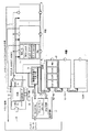
FIG. 1 is a diagram showing an example of the configuration of the source driver IC1 according to the first embodiment of the present invention. The source driver IC1 replaces the
図1に示すように、ソースドライバーIC1は、VDDA入力端子2と、比較回路3と、判定回路4と、制御スイッチ10(第1の制御スイッチ)と、制御スイッチ11(第2の制御スイッチ)とを備えることを特徴としている。その他の構成は、図14に示すドライバーICの構成と同様であるため、ここでは詳細な説明を省略する。
As shown in FIG. 1, the
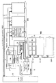
ソースドライバーICには、ロジック用の電源(VDDD)と、アナログ回路用の電源(VDDA)とがある。図2に示すように、一般的なソースドライバーIC13では、同電位の端子同士をまとめて配線している。図2の例では、同電位のVDDA接続端子15をまとめて配線し、ソースドライバーIC13のVDDA入力端子14に接続する場合の一例を示している。VDDA接続端子15は、液晶パネル12の周縁部に配置されており、FPC27に設けられた端子と接続可能となっている。なお、ソースドライバーIC13は、図13のソースドライバーIC32であってもよい。液晶パネル12は、液晶パネル30(図11,12参照)であってもよい。
The source driver IC includes a power supply for logic (VDDD) and a power supply for analog circuits (VDDA). As shown in FIG. 2, in a general
一方、図3に示すように、本実施の形態1では、VDDA接続端子17において外部から入力されたVDDA(アナログ電源)がVDDA1(第1のアナログ電源)の端子とVDDA2(第2のアナログ電源)の端子とに物理的に分離されており、ソースドライバーIC1のVDDA入力端子2においてもVDDA1の端子とVDDA2の端子とに物理的に分離されている。VDDA入力端子2におけるVDDA1の端子およびVDDA2の端子の各々は、比較回路3に接続されている。VDDA接続端子17は、液晶パネル16の周縁部に配置されており、FPC27に設けられたVDDAの端子と接続可能となっている。なお、液晶パネル16は、液晶パネル30(図11,12参照)であってもよい。
On the other hand, as shown in FIG. 3, in the first embodiment, VDDA (analog power supply) input from the outside at
比較回路3は、例えば図4に示すようなコンパレーターを有しており、VDDA1の電位とVDDA2の電位との電位差を検出し、検出した電位差を2値論理に変換してから判定回路4に出力する。
The
判定回路4は、比較回路3で検出された電位差が予め定められた閾値以上である場合に異常状態であると判定する。例えば、判定回路4は、比較回路3から入力された2値論理が「H」である場合において異常状態であると判定する。判定回路4による判定結果は、電流制御回路5に出力される。
The
電流制御回路5(図15参照)は、判定回路4から異常状態である旨の信号(入力選択信号)が入力されると、出力アンプに入力する電流量が少なくなるように切り替える(例えば、AからDに切り替える)。すなわち、判定回路4が異常状態であると判定した場合において、電流制御回路5は、出力アンプ6から画素領域31(図11,12参照)に出力される電流量が少なくなるように制御する。
When a signal indicating an abnormal state (input selection signal) is input from the
また、判定回路4が異常状態であると判定した場合において、制御スイッチ10,11は、判定回路4から異常状態である旨の信号が入力されると、アシスト回路8が異常に動作しないように、すなわちPMOSトランジスタおよびNMOSトランジスタが同時にONしないように制御する。
Further, when the
なお、判定回路4は、異常状態であると判定した場合において、異常状態である旨をシステム側(図示しない)に出力可能にしてもよい。例えば、図5に示すように、ソースドライバーIC1にモニタ端子18を設け、異常状態である旨の信号(モニタ信号)を、モニタ端子18を介してTCON19に出力してもよい(図6参照)。図6において、TCON19は、ソースドライバーIC1から入力されたモニタ信号を認識した後、エラー信号としてインターフェースコネクタ20を介してシステム側に出力することができる。
When the
また、異常状態である旨をシステム側に出力する他の方法として、図7に示すように、異常状態である旨の信号(モニタ信号)を、モニタ端子18を介してインターフェースコネクタ20に直接出力するようにしてもよい。この場合、システム側では、異常状態を直接モニタすることができる。
Further, as another method of outputting the abnormal state to the system side, as shown in FIG. 7 , a signal (monitor signal) indicating the abnormal state is directly output to the
以上のことから、本実施の形態1によれば、低負荷時のアシスト回路8における貫通電流の発生を抑制することができる。従って、VDDAの電流値を下げることができ、液晶表示装置の全体的な消費電力を下げることができる。また、液晶パネルが異常状態であるか否かを簡単にモニタすることができる。近年、車載の機能安全規格であるISO26262を意識したシステム構築を行う上でそのリスク管理が問われるが、本実施の形態1によれば異常状態(例えば、断線状態)を監視(モニタ)することができる。異常状態をシステム側で監視することが可能であり、仮に液晶パネルが異常状態になったとしても表示自体は行うことができるため、液晶パネルの状態を画面に表示してユーザーに知らせることが可能である。そして、液晶パネルが異常状態である場合は、ユーザーに対して異常状態に対する対処を促すことも可能である。
From the above, according to the first embodiment, it is possible to suppress the generation of the through current in the
<実施の形態2>
実施の形態1では、図3に示すVDDA1およびVDDA2を電源回路23から出力されるVDDAに共通して接続する場合について説明した。本発明の実施の形態2では、図8に示すように、レギュレータ回路などの安定化回路であるVDDA2生成部29を備えることを特徴としている。なお、VDDA1およびVDDA2以外にVDDD端子やGND端子、設定端子、何も接続しないダミー端子などその他の端子については、「その他」と記載して省略している。構成および動作は、実施の形態1と同様であるため、ここでは詳細な説明を省略する。
<
In the first embodiment, a case where VDDA1 and VDDA2 shown in FIG. 3 are commonly connected to VDDA output from the
図8に示すように、電源回路23のVDDA生成部28から出力されたVDDAは、VDDA1とVDDA2とに分離される。そして、VDDA2に対して安定化回路であるVDDA2生成部29を備え、VDDA2生成部29で生成されたVDDA2は、FPC27を介してソースドライバーIC1のVDDA入力端子2におけるVDDA2の端子に入力される。この場合、VDDA2は、出力アンプ6の電源(電流源)として供給されるVDDA1と完全に分離される。
As shown in FIG. 8, VDDA output from
以上のことから、本実施の形態2によれば、VDDA2については、図16に示すような負荷変動を抑制することができる。従って、負荷変動を受けるVDDA1との比較が容易となり、アシスト回路8の不安定な動作をより検出し易くなる。
From the above, according to the second embodiment, the load fluctuation as shown in FIG. 16 can be suppressed for VDDA2. Therefore, it becomes easy to compare with VDDA1 which is subject to load fluctuation, and it becomes easier to detect unstable operation of the
<実施の形態3>
本発明の実施の形態3では、図9に示すように、液晶パネル16に設けられたVDDA接続端子17におけるVDDA2の端子をFPC27の端側部に対応する位置に配置することを特徴としている。その他の構成および動作は、実施の形態1または2と同様であるため、ここでは詳細な説明を省略する。
<
The third embodiment of the present invention is characterized in that, as shown in FIG. 9, the terminal of VDDA2 in the
図11,12に示す液晶表示装置に対して振動または衝撃などのストレスが加わると、FPC27の端側部に応力がかかりやすくなり、FPC27の端部(特に、端側部)から断線しやすくなる。図9に示すように、液晶パネル16に設けられたVDDA接続端子17におけるVDDA2の端子(第2の接続端子)をFPC27の端側部に対応する位置に配置した場合において、液晶表示装置に対してストレスが加わると、FPC27の端部の中央側に配置されたVDDA1の端子(第1の接続端子)に接続された配線よりも、端側部に配置されたVDDA2の端子に接続された配線の方が先に断線することになる。断線した配線の抵抗値は大きく上昇する。液晶パネル16の配線抵抗と異方性導電膜(ACF:Anisotropic Conductive Film)の抵抗とを合計すると、電源およびGNDラインは通常10Ω以下程度の抵抗値になることが多い(FPCと回路基板26上の銅配線部分とは、1Ωよりもはるかに小さいレベルの低抵抗であるため、液晶パネル30における配線抵抗のばらつきと比較して無視できるレベルである)。また、完全に断線した場合の抵抗値はMΩオーダーになるが、断線しかかっている場合の抵抗値は通常時の抵抗値と断線時の抵抗値との間の値となる。
When stress such as vibration or impact is applied to the liquid crystal display device shown in FIGS. 11 and 12, stress is likely to be applied to the end side portion of the
以上のことから、本実施の形態3によれば、VDDA1の配線よりも先にVDDA2の配線が断線するとVDDA2の配線の抵抗値が上昇し、これを比較回路3が検出することができる。また、比較回路3による検出結果に基づいて判定回路4で異常状態を判定し、その結果をシステム側に出力することによって、システム側でVDDA2の断線をモニタすることができるようになる。
From the above, according to the third embodiment, if the wiring of VDDA2 is disconnected before the wiring of VDDA1, the resistance value of the wiring of VDDA2 increases, and the
なお、本発明は、その発明の範囲内において、各実施の形態を自由に組み合わせたり、各実施の形態を適宜、変形、省略することが可能である。また、回路ブロックの一部が他の部品のブロックに移動した形態も可能である。例えば、TCON19がソースドライバーIC内部に踏襲されたTCON内蔵ドライバーICのケースでは、図6,7のRSDS Tx/Rx部分は削除される。あるいは電源回路23と階調参照電圧生成回路24が一体となったもの、電源回路23または階調参照電圧生成回路24の一部がソースドライバーIC1、またはゲートドライバーIC22に踏襲された形態も可能である。
In the present invention, each embodiment can be freely combined, and each embodiment can be appropriately modified or omitted within the scope of the invention. It is also possible that a part of the circuit block is moved to a block of another component. For example, in the case of the TCON built-in driver IC in which the
1 ソースドライバーIC、2 VDDA入力端子、3 比較回路、4 判定回路、5 電流制御回路、6 出力アンプ、7 アンプ出力制御回路、8 アシスト回路、9 スイッチ、10,11 制御スイッチ、12 液晶パネル、13 ソースドライバーIC、14 VDDA入力端子、15 VDDA接続端子、16 液晶パネル、17 VDDA接続端子、18 モニタ端子、19 TCON、20 インターフェースコネクタ、21 EEPROM、22 ゲートドライバーIC、23 電源回路、24 階調参照電圧生成回路、25 液晶パネル、26 回路基板、27 FPC、28 VDDA生成部、29 VDDA2生成部、30 液晶パネル、31 画素領域。 1 Source driver IC, 2 VDDA input terminal, 3 Comparison circuit, 4 Judgment circuit, 5 Current control circuit, 6 Output amplifier, 7 Amplifier output control circuit, 8 Assist circuit, 9 switch, 10, 11 control switch, 12 LCD panel, 13 Source driver IC, 14 VDDA input terminal, 15 VDDA connection terminal, 16 LCD panel, 17 VDDA connection terminal, 18 monitor terminal, 19 TCON, 20 interface connector, 21 EEPROM, 22 gate driver IC, 23 power supply circuit, 24 gradations Reference voltage generation circuit, 25 liquid crystal panel, 26 circuit board, 27 FPC, 28 VDDA generation unit, 29 VDDA2 generation unit, 30 liquid crystal panel, 31 pixel area.
Claims (6)
外部から入力されたアナログ電源であって、分離された第1のアナログ電源の電位と第2のアナログ電源の電位とを比較して電位差を検出する比較回路と、
前記比較回路で検出された前記電位差が予め定められた閾値以上である場合に異常状態であると判定する判定回路と、
を備え、
出力アンプと、
PMOSトランジスタおよびNMOSトランジスタと、前記PMOSトランジスタおよび前記NMOSトランジスタが同時にONして大電流が出力されないように設けられた第1の回路および第2の回路とを有し、前記出力アンプから前記画素領域への出力を補助する補助回路と、
一端が前記判定回路に接続され、他端が前記第1の回路を介して前記PMOSトランジスタのゲートに接続され、前記PMOSトランジスタ自体の動作を制御する第1の制御スイッチと、
一端が前記判定回路に接続され、他端が前記第2の回路を介して前記NMOSトランジスタのゲートに接続され、前記NMOSトランジスタ自体の動作を制御する第2の制御スイッチと、
をさらに備え、
前記判定回路が前記異常状態であると判定した場合において、
前記第1の制御スイッチおよび前記第2の制御スイッチの各々は、前記PMOSトランジスタおよび前記NMOSトランジスタが同時にONしないように制御し、
前記第1のアナログ電源は、前記比較回路、前記補助回路、および前記出力アンプに供給され、
前記第2のアナログ電源は、前記比較回路に供給され、
前記異常状態は、前記PMOSトランジスタおよび前記NMOSトランジスタが同時にONして貫通電流が発生する状態であることを特徴とする、駆動装置。 A drive device provided in a liquid crystal panel that drives a pixel region of the liquid crystal panel.
A comparison circuit that detects the potential difference by comparing the potential of the separated first analog power supply and the potential of the second analog power supply, which is an analog power supply input from the outside.
A determination circuit for determining an abnormal state when the potential difference detected by the comparison circuit is equal to or greater than a predetermined threshold value, and
With
With the output amplifier
It has a MOSFET transistor and an NMOS transistor, and a first circuit and a second circuit provided so that the NMOS transistor and the NMOS transistor are turned on at the same time and a large current is not output, and the pixel area from the output amplifier. Auxiliary circuit to assist the output to
One end connected to said decision circuit, the other end is connected to the gate of the PMOS transistor through said first circuit, a first control switch for controlling the operation of the PMOS transistor itself,
One end connected to said decision circuit, the other end is connected to the gate of the NMOS transistor through the second circuit, the second control switch for controlling the operation of the NMOS transistor itself,
With more
When the determination circuit determines that the abnormal state is present,
Each of the first control switch and the second control switch controls so that the NMOS transistor and the NMOS transistor are not turned on at the same time.
The first analog power supply is supplied to the comparison circuit, the auxiliary circuit, and the output amplifier.
The second analog power supply is supplied to the comparison circuit.
The driving device is characterized in that the abnormal state is a state in which the NMOS transistor and the NMOS transistor are turned on at the same time to generate a through current.
前記電流制御回路は、前記判定回路が前記異常状態であると判定した場合において、前記出力アンプから出力される前記電流量が少なくなるように制御することを特徴とする、請求項1に記載の駆動装置。 A current control circuit for controlling the amount of current output from the output amplifier to the pixel region is further provided.
The first aspect of the present invention, wherein the current control circuit is controlled so that the amount of the current output from the output amplifier is reduced when the determination circuit determines that the abnormal state is present. Drive device.
前記液晶パネルは、前記第1のアナログ電源について前記FPCと接続可能な第1の接続端子と、前記第2のアナログ電源について前記FPCと接続可能な第2の接続端子とを備え、
前記第2の接続端子は、前記FPCの端側部に対応する位置に配置されることを特徴とする、請求項4に記載の液晶表示装置。 The first analog power supply and the second analog power supply are supplied to the drive device via an FPC (Flexible Printed Circuit).
The liquid crystal panel includes a first connection terminal that can be connected to the FPC for the first analog power supply and a second connection terminal that can be connected to the FPC for the second analog power supply.
Before Stories second connection pin is characterized in that it is arranged at a position corresponding to the side edge of the FPC, the liquid crystal display device according to claim 4.
Priority Applications (4)
| Application Number | Priority Date | Filing Date | Title |
|---|---|---|---|
| JP2016013309A JP6903398B2 (en) | 2016-01-27 | 2016-01-27 | Drive device and liquid crystal display device |
| US15/397,823 US10720119B2 (en) | 2016-01-27 | 2017-01-04 | Drive device and liquid crystal display apparatus |
| DE102017201229.3A DE102017201229A1 (en) | 2016-01-27 | 2017-01-26 | Driver device and liquid crystal display device |
| CN201710063288.0A CN107016968B (en) | 2016-01-27 | 2017-02-03 | Driving device and liquid crystal display device |
Applications Claiming Priority (1)
| Application Number | Priority Date | Filing Date | Title |
|---|---|---|---|
| JP2016013309A JP6903398B2 (en) | 2016-01-27 | 2016-01-27 | Drive device and liquid crystal display device |
Publications (3)
| Publication Number | Publication Date |
|---|---|
| JP2017134203A JP2017134203A (en) | 2017-08-03 |
| JP2017134203A5 JP2017134203A5 (en) | 2019-02-28 |
| JP6903398B2 true JP6903398B2 (en) | 2021-07-14 |
Family
ID=59295965
Family Applications (1)
| Application Number | Title | Priority Date | Filing Date |
|---|---|---|---|
| JP2016013309A Active JP6903398B2 (en) | 2016-01-27 | 2016-01-27 | Drive device and liquid crystal display device |
Country Status (4)
| Country | Link |
|---|---|
| US (1) | US10720119B2 (en) |
| JP (1) | JP6903398B2 (en) |
| CN (1) | CN107016968B (en) |
| DE (1) | DE102017201229A1 (en) |
Families Citing this family (6)
| Publication number | Priority date | Publication date | Assignee | Title |
|---|---|---|---|---|
| JP6706954B2 (en) * | 2016-04-01 | 2020-06-10 | 三菱電機株式会社 | Driver IC and liquid crystal display device |
| JP7371455B2 (en) * | 2019-11-21 | 2023-10-31 | セイコーエプソン株式会社 | Drive circuit, display module, and moving object |
| KR20210103043A (en) * | 2020-02-12 | 2021-08-23 | 삼성디스플레이 주식회사 | Power voltage generator, method of controlling the same and display apparatus having the same |
| JP7266057B2 (en) | 2021-03-24 | 2023-04-27 | 本田技研工業株式会社 | vehicle |
| CN215986461U (en) * | 2021-06-11 | 2022-03-08 | 五邑大学 | Sound source positioning system based on microphone array |
| CN116049863B (en) * | 2023-03-28 | 2023-06-13 | 东莞锐视光电科技有限公司 | System, method and application for generating stripe light by LCD display screen |
Family Cites Families (69)
| Publication number | Priority date | Publication date | Assignee | Title |
|---|---|---|---|---|
| JP2536210B2 (en) * | 1989-02-03 | 1996-09-18 | 日本電気株式会社 | Power supply voltage monitoring circuit |
| JPH0541651A (en) | 1991-08-06 | 1993-02-19 | Fuji Electric Co Ltd | Semiconductor integrated circuit device for capacity load driving |
| US5136186A (en) * | 1991-08-30 | 1992-08-04 | Waferscale Integration, Incorporation | Glitch free power-up for a programmable array |
| US5481194A (en) * | 1994-06-10 | 1996-01-02 | Westinghouse Electric Corp. | Fault detection circuit for sensing leakage currents between power source and chassis |
| FR2749939B1 (en) * | 1996-06-13 | 1998-07-31 | Sgs Thomson Microelectronics | SUPPLY VOLTAGE RANGE DETECTOR IN AN INTEGRATED CIRCUIT |
| JP3427637B2 (en) * | 1996-09-30 | 2003-07-22 | ヤマハ株式会社 | Reference voltage generation circuit |
| JPH10133754A (en) * | 1996-10-28 | 1998-05-22 | Fujitsu Ltd | Regulator circuit and semiconductor integrated circuit device |
| JPH10288634A (en) * | 1997-04-16 | 1998-10-27 | Nec Ic Microcomput Syst Ltd | Supply voltage detecting circuit |
| US6085342A (en) * | 1997-05-06 | 2000-07-04 | Telefonaktiebolaget L M Ericsson (Publ) | Electronic system having a chip integrated power-on reset circuit with glitch sensor |
| JPH11213664A (en) * | 1998-01-23 | 1999-08-06 | Mitsubishi Electric Corp | Semiconductor integrated-circuit device |
| JP4032539B2 (en) | 1998-12-01 | 2008-01-16 | 三菱電機株式会社 | Data line drive circuit for matrix display |
| JP3508837B2 (en) * | 1999-12-10 | 2004-03-22 | インターナショナル・ビジネス・マシーンズ・コーポレーション | Liquid crystal display device, liquid crystal controller, and video signal transmission method |
| JP2001255857A (en) | 2000-03-09 | 2001-09-21 | Texas Instr Japan Ltd | Driving circuit |
| JP3578043B2 (en) * | 2000-04-14 | 2004-10-20 | 松下電器産業株式会社 | Power supply voltage detection circuit |
| JP2002041159A (en) * | 2000-07-25 | 2002-02-08 | Nec Yamagata Ltd | Semiconductor integrated circuit device |
| DE10120147B4 (en) * | 2001-04-25 | 2010-08-05 | Nxp B.V. | Circuit for detecting short voltage dips in a supply voltage |
| US6642706B2 (en) * | 2001-06-13 | 2003-11-04 | Koninklijke Philips Electronics N.V. | Detection of asymmetrical load in an AC circuit |
| JP3813477B2 (en) | 2001-09-12 | 2006-08-23 | シャープ株式会社 | Power supply device and display device having the same |
| KR100440451B1 (en) * | 2002-05-31 | 2004-07-14 | 삼성전자주식회사 | Circuit For Detecting A Volatage Glitch, An Integrated Circuit Device Having The Same, And An Apparatus And Method For Securing An Integrated Circuit Device From A Voltage Glitch Attack |
| JP3649211B2 (en) | 2002-06-20 | 2005-05-18 | セイコーエプソン株式会社 | Driving circuit, electro-optical device, and driving method |
| AU2003247111A1 (en) * | 2002-08-21 | 2004-03-11 | Koninklijke Philips Electronics N.V. | Display device |
| JP2004354518A (en) | 2003-05-27 | 2004-12-16 | Sharp Corp | Driving voltage generating circuit and liquid crystal drive device using the same |
| US7119529B2 (en) * | 2003-06-12 | 2006-10-10 | Koninklijke Philips Electronics N.V. | Circuit arrangement with a resistor voltage divider chain |
| JP2005208551A (en) | 2003-12-25 | 2005-08-04 | Sharp Corp | Display device and driving device |
| CN100474206C (en) * | 2003-12-26 | 2009-04-01 | 松下电器产业株式会社 | Semiconductor device |
| KR100996573B1 (en) * | 2003-12-30 | 2010-11-24 | 엘지디스플레이 주식회사 | Analog buffer and method for driving the same |
| KR100698983B1 (en) | 2004-03-30 | 2007-03-26 | 샤프 가부시키가이샤 | Display device and driving device |
| KR100574489B1 (en) * | 2004-04-12 | 2006-04-27 | 주식회사 하이닉스반도체 | Internal Voltage Generating Circuit of Semiconductor Memory Device |
| CN101192378A (en) | 2006-11-22 | 2008-06-04 | 硕颉科技股份有限公司 | System capable of regulating drive ability of output stage |
| JP4885706B2 (en) | 2006-12-28 | 2012-02-29 | 富士通株式会社 | Power supply monitoring and control device for display device |
| US7589568B2 (en) * | 2007-05-04 | 2009-09-15 | Microchip Technology Incorporated | Variable power and response time brown-out-reset circuit |
| JP4277055B2 (en) * | 2007-05-29 | 2009-06-10 | シャープ株式会社 | Drive circuit, display device, and television system |
| US7663439B2 (en) * | 2007-12-06 | 2010-02-16 | Himax Technologies Limited | Operational amplifier |
| CN101604282B (en) * | 2008-06-13 | 2012-08-29 | 鸿富锦精密工业(深圳)有限公司 | Voltage detection alarm device |
| KR101501663B1 (en) * | 2008-08-08 | 2015-03-11 | 삼성디스플레이 주식회사 | Method for data driving a display panel, data deriving circuit for performing the method and desplay device having the same |
| JP2010146526A (en) * | 2008-12-22 | 2010-07-01 | Panasonic Corp | Reference voltage generating circuit |
| KR101581723B1 (en) * | 2008-12-26 | 2015-12-31 | 주식회사 동부하이텍 | Amp output protective circuit for lcd panel source driver and method thereof |
| US8169425B2 (en) * | 2009-01-14 | 2012-05-01 | Himax Technologies Limited | Source driver adapted to a display panel |
| US20120038614A1 (en) * | 2009-02-23 | 2012-02-16 | Hidetaka Mizumaki | Display device and driving device |
| US8508515B2 (en) | 2009-08-05 | 2013-08-13 | Himax Technologies Limited | Buffering circuit with reduced dynamic power consumption |
| TWI419609B (en) * | 2009-08-19 | 2013-12-11 | Novatek Microelectronics Corp | Led device with simultaneous open and short detection function and method thereof |
| US8212762B2 (en) * | 2009-10-13 | 2012-07-03 | Himax Technologies Limited | Output amplifier of a source driver with an amplifier circuit having an inverted and non-inverted output |
| US8279156B2 (en) * | 2009-10-13 | 2012-10-02 | Himax Technologies Limited | Output amplifier of source driver with high impedance and inverted high impedance control signals |
| JP5535608B2 (en) * | 2009-12-21 | 2014-07-02 | ラピスセミコンダクタ株式会社 | Voltage change detector |
| JP5457220B2 (en) | 2010-02-18 | 2014-04-02 | ルネサスエレクトロニクス株式会社 | Output circuit, data driver, and display device |
| JP2011172066A (en) * | 2010-02-19 | 2011-09-01 | Renesas Electronics Corp | Operational amplifier, as well as display panel driver and display device using the same |
| TWI406468B (en) * | 2010-04-27 | 2013-08-21 | Richtek Technology Corp | Protection apparatus and method for avoiding abnormal system operation caused by a shorted parameter setting pin of an ic |
| US8487924B2 (en) * | 2010-08-25 | 2013-07-16 | Dongwoon Anatech Co., Ltd. | Apparatus for driving of display panel |
| TWI427590B (en) * | 2010-09-02 | 2014-02-21 | Novatek Microelectronics Corp | Display apparatus and display method thereof |
| US8817429B2 (en) * | 2010-11-23 | 2014-08-26 | Samsung Display Co., Ltd. | Power converter, display device including power converter, system including display device, and method of driving display device |
| US8564585B2 (en) * | 2010-12-09 | 2013-10-22 | Himax Technologies Limited | Source driver and display device with protection unit |
| CN102103844A (en) | 2011-01-30 | 2011-06-22 | 友达光电股份有限公司 | Power management method |
| WO2012137886A1 (en) * | 2011-04-08 | 2012-10-11 | シャープ株式会社 | Display device, and method for driving display device |
| KR101860739B1 (en) * | 2011-05-18 | 2018-05-25 | 삼성디스플레이 주식회사 | Supply voltage converter, display device including the same and method of controlling driving voltage |
| JP2013021117A (en) * | 2011-07-11 | 2013-01-31 | Rohm Co Ltd | Led drive device, luminaire, and liquid crystal display device |
| CN102971780B (en) * | 2011-07-11 | 2015-11-25 | 株式会社日本有机雷特显示器 | Display device |
| US8946994B2 (en) * | 2012-09-25 | 2015-02-03 | Lg Display Co., Ltd. | Organic light emitting display device and driving method thereof |
| KR101940220B1 (en) * | 2012-10-23 | 2019-01-18 | 엘지디스플레이 주식회사 | Display Device Including Power Control Unit And Method Of Driving The Same |
| US9230490B2 (en) * | 2012-12-25 | 2016-01-05 | Shenzhen China Star Optoelectronics Technology Co., Ltd | LED backlight driver circuit |
| KR102081923B1 (en) * | 2013-02-04 | 2020-02-26 | 삼성전자주식회사 | Memory system and operating method of meomry controller |
| CN103280847B (en) | 2013-04-22 | 2015-04-08 | 京东方科技集团股份有限公司 | Power supply circuit and display device |
| US9203423B2 (en) * | 2013-08-22 | 2015-12-01 | Mediatek Inc. | Class AB signal generation apparatus |
| JP6180318B2 (en) * | 2013-12-27 | 2017-08-16 | ソニーセミコンダクタソリューションズ株式会社 | Comparator circuit |
| TWI526113B (en) * | 2014-08-13 | 2016-03-11 | 緯創資通股份有限公司 | Light emitting diode driving chip, drving system appling the light emitting diode driving chip, and method thereof |
| US9871390B2 (en) * | 2014-09-02 | 2018-01-16 | Silergy Corp. | Battery protection integrated circuit applied to battery charging/discharging system and method for determining resistances of voltage divider of battery protection integrated circuit |
| KR102289459B1 (en) * | 2015-03-11 | 2021-08-17 | 삼성디스플레이 주식회사 | Backlight unit, display apparatus having the same and operating method of backlight unit |
| US9989574B2 (en) * | 2015-05-27 | 2018-06-05 | Infineon Technologies Ag | System and method for short-circuit detection in load chains |
| KR102594096B1 (en) * | 2016-02-23 | 2023-10-26 | 삼성디스플레이 주식회사 | Short detection circuit and display device including the same |
| JP6139747B1 (en) * | 2016-05-10 | 2017-05-31 | 三菱電機株式会社 | Discharge device |
-
2016
- 2016-01-27 JP JP2016013309A patent/JP6903398B2/en active Active
-
2017
- 2017-01-04 US US15/397,823 patent/US10720119B2/en active Active
- 2017-01-26 DE DE102017201229.3A patent/DE102017201229A1/en active Granted
- 2017-02-03 CN CN201710063288.0A patent/CN107016968B/en active Active
Also Published As
| Publication number | Publication date |
|---|---|
| DE102017201229A1 (en) | 2017-07-27 |
| US10720119B2 (en) | 2020-07-21 |
| JP2017134203A (en) | 2017-08-03 |
| CN107016968A (en) | 2017-08-04 |
| US20170213518A1 (en) | 2017-07-27 |
| CN107016968B (en) | 2020-03-13 |
Similar Documents
| Publication | Publication Date | Title |
|---|---|---|
| JP6903398B2 (en) | Drive device and liquid crystal display device | |
| US9183340B2 (en) | Electronic device having circuit board with co-layout design of multiple connector placement sites and related circuit board thereof | |
| US10354571B2 (en) | Driver IC including an abnormality detection part for detecting abnormalities, a waveform-changing part for changing waveforms, and an output part for outputting signals, and liquid crystal display device comprising the same | |
| CN101656057B (en) | Timing control apparatus and display device having the same | |
| US20080084371A1 (en) | Liquid crystal display for preventing residual image phenomenon and related method thereof | |
| US9466238B2 (en) | Display device and driving method thereof | |
| KR20060097552A (en) | Driving system of liquid crystal display | |
| CN107808645B (en) | Display device and power monitoring circuit | |
| TWI720552B (en) | Integrated circuit and touch display apparatus | |
| US8106638B2 (en) | Power control circuit with coupling circuit for controlling output power sequence and liquid crystal display using same | |
| US20180188880A1 (en) | Touch substrate and touch display device | |
| CN110706628A (en) | Display device and state detection method thereof | |
| CN114242014B (en) | COF temperature control circuit, driving method and terminal equipment | |
| KR102276248B1 (en) | A display device and a protection method thereof | |
| CN210136712U (en) | Display driving chip, display panel, display device and display system | |
| KR20210031587A (en) | Display device and driving method thereof | |
| JP2006106077A (en) | Electrooptical apparatus and electronic device | |
| KR101619324B1 (en) | Liquid crystal display device and method of driving the same | |
| KR20160083370A (en) | Display Device | |
| KR101847701B1 (en) | High resolution display and driver chip thereof | |
| JP2020140017A (en) | Drive circuit, liquid crystal drive controller, and liquid crystal display device | |
| US7916132B2 (en) | Systems for displaying images and related methods | |
| US20240038118A1 (en) | Display apparatus | |
| KR102419655B1 (en) | Power supply unit and display device comprising the power supply unit | |
| TW202236070A (en) | Touch power management circuit and touch driving system |
Legal Events
| Date | Code | Title | Description |
|---|---|---|---|
| A521 | Written amendment |
Free format text: JAPANESE INTERMEDIATE CODE: A523 Effective date: 20190110 |
|
| A621 | Written request for application examination |
Free format text: JAPANESE INTERMEDIATE CODE: A621 Effective date: 20190110 |
|
| A977 | Report on retrieval |
Free format text: JAPANESE INTERMEDIATE CODE: A971007 Effective date: 20191017 |
|
| A131 | Notification of reasons for refusal |
Free format text: JAPANESE INTERMEDIATE CODE: A131 Effective date: 20191126 |
|
| A521 | Written amendment |
Free format text: JAPANESE INTERMEDIATE CODE: A523 Effective date: 20200120 |
|
| A02 | Decision of refusal |
Free format text: JAPANESE INTERMEDIATE CODE: A02 Effective date: 20200421 |
|
| A521 | Written amendment |
Free format text: JAPANESE INTERMEDIATE CODE: A523 Effective date: 20200616 |
|
| C60 | Trial request (containing other claim documents, opposition documents) |
Free format text: JAPANESE INTERMEDIATE CODE: C60 Effective date: 20200616 |
|
| A911 | Transfer of reconsideration by examiner before appeal (zenchi) |
Free format text: JAPANESE INTERMEDIATE CODE: A911 Effective date: 20200624 |
|
| C21 | Notice of transfer of a case for reconsideration by examiners before appeal proceedings |
Free format text: JAPANESE INTERMEDIATE CODE: C21 Effective date: 20200630 |
|
| A912 | Removal of reconsideration by examiner before appeal (zenchi) |
Free format text: JAPANESE INTERMEDIATE CODE: A912 Effective date: 20200904 |
|
| C211 | Notice of termination of reconsideration by examiners before appeal proceedings |
Free format text: JAPANESE INTERMEDIATE CODE: C211 Effective date: 20200908 |
|
| C22 | Notice of designation (change) of administrative judge |
Free format text: JAPANESE INTERMEDIATE CODE: C22 Effective date: 20201208 |
|
| C13 | Notice of reasons for refusal |
Free format text: JAPANESE INTERMEDIATE CODE: C13 Effective date: 20210216 |
|
| A521 | Written amendment |
Free format text: JAPANESE INTERMEDIATE CODE: A523 Effective date: 20210413 |
|
| C23 | Notice of termination of proceedings |
Free format text: JAPANESE INTERMEDIATE CODE: C23 Effective date: 20210511 |
|
| C03 | Trial/appeal decision taken |
Free format text: JAPANESE INTERMEDIATE CODE: C03 Effective date: 20210615 |
|
| C30A | Notification sent |
Free format text: JAPANESE INTERMEDIATE CODE: C3012 Effective date: 20210615 |
|
| A61 | First payment of annual fees (during grant procedure) |
Free format text: JAPANESE INTERMEDIATE CODE: A61 Effective date: 20210623 |
|
| R150 | Certificate of patent or registration of utility model |
Ref document number: 6903398 Country of ref document: JP Free format text: JAPANESE INTERMEDIATE CODE: R150 |