JP6873141B2 - Dynamic filtering system and method - Google Patents
Dynamic filtering system and method Download PDFInfo
- Publication number
- JP6873141B2 JP6873141B2 JP2018533936A JP2018533936A JP6873141B2 JP 6873141 B2 JP6873141 B2 JP 6873141B2 JP 2018533936 A JP2018533936 A JP 2018533936A JP 2018533936 A JP2018533936 A JP 2018533936A JP 6873141 B2 JP6873141 B2 JP 6873141B2
- Authority
- JP
- Japan
- Prior art keywords
- analog electrical
- electrical waveform
- analog
- input
- delay
- Prior art date
- Legal status (The legal status is an assumption and is not a legal conclusion. Google has not performed a legal analysis and makes no representation as to the accuracy of the status listed.)
- Active
Links
- 238000000034 method Methods 0.000 title claims description 27
- 238000001914 filtration Methods 0.000 title claims description 24
- 239000000523 sample Substances 0.000 claims description 27
- 230000003111 delayed effect Effects 0.000 claims description 22
- 239000000872 buffer Substances 0.000 claims description 17
- 238000003384 imaging method Methods 0.000 claims description 17
- 238000005070 sampling Methods 0.000 claims description 15
- 230000001934 delay Effects 0.000 claims description 10
- 230000001066 destructive effect Effects 0.000 claims description 9
- 230000002238 attenuated effect Effects 0.000 claims description 6
- 230000015572 biosynthetic process Effects 0.000 description 13
- 239000003990 capacitor Substances 0.000 description 12
- 238000013459 approach Methods 0.000 description 8
- 238000012545 processing Methods 0.000 description 8
- 230000008901 benefit Effects 0.000 description 7
- 230000006870 function Effects 0.000 description 6
- 210000001519 tissue Anatomy 0.000 description 6
- 239000002872 contrast media Substances 0.000 description 5
- 230000008569 process Effects 0.000 description 5
- 230000004044 response Effects 0.000 description 5
- 238000004088 simulation Methods 0.000 description 5
- 238000001228 spectrum Methods 0.000 description 5
- 230000000903 blocking effect Effects 0.000 description 3
- 230000009286 beneficial effect Effects 0.000 description 2
- 239000004020 conductor Substances 0.000 description 2
- 238000010586 diagram Methods 0.000 description 2
- 230000003993 interaction Effects 0.000 description 2
- 230000035945 sensitivity Effects 0.000 description 2
- 238000002604 ultrasonography Methods 0.000 description 2
- 101000786631 Homo sapiens Protein SYS1 homolog Proteins 0.000 description 1
- 235000014676 Phragmites communis Nutrition 0.000 description 1
- 102100025575 Protein SYS1 homolog Human genes 0.000 description 1
- 230000003321 amplification Effects 0.000 description 1
- 210000004369 blood Anatomy 0.000 description 1
- 239000008280 blood Substances 0.000 description 1
- 238000006243 chemical reaction Methods 0.000 description 1
- 230000001427 coherent effect Effects 0.000 description 1
- 238000004891 communication Methods 0.000 description 1
- 229940039231 contrast media Drugs 0.000 description 1
- 238000011161 development Methods 0.000 description 1
- 239000006185 dispersion Substances 0.000 description 1
- 230000009977 dual effect Effects 0.000 description 1
- 230000000694 effects Effects 0.000 description 1
- 230000020169 heat generation Effects 0.000 description 1
- 230000001788 irregular Effects 0.000 description 1
- 210000005228 liver tissue Anatomy 0.000 description 1
- 238000004519 manufacturing process Methods 0.000 description 1
- 238000012986 modification Methods 0.000 description 1
- 230000004048 modification Effects 0.000 description 1
- 210000004165 myocardium Anatomy 0.000 description 1
- 238000003199 nucleic acid amplification method Methods 0.000 description 1
- 238000013139 quantization Methods 0.000 description 1
- 230000009467 reduction Effects 0.000 description 1
- 238000009738 saturating Methods 0.000 description 1
Images


Classifications
-
- G—PHYSICS
- G01—MEASURING; TESTING
- G01S—RADIO DIRECTION-FINDING; RADIO NAVIGATION; DETERMINING DISTANCE OR VELOCITY BY USE OF RADIO WAVES; LOCATING OR PRESENCE-DETECTING BY USE OF THE REFLECTION OR RERADIATION OF RADIO WAVES; ANALOGOUS ARRANGEMENTS USING OTHER WAVES
- G01S15/00—Systems using the reflection or reradiation of acoustic waves, e.g. sonar systems
- G01S15/88—Sonar systems specially adapted for specific applications
- G01S15/89—Sonar systems specially adapted for specific applications for mapping or imaging
- G01S15/8906—Short-range imaging systems; Acoustic microscope systems using pulse-echo techniques
- G01S15/8909—Short-range imaging systems; Acoustic microscope systems using pulse-echo techniques using a static transducer configuration
- G01S15/8915—Short-range imaging systems; Acoustic microscope systems using pulse-echo techniques using a static transducer configuration using a transducer array
- G01S15/8927—Short-range imaging systems; Acoustic microscope systems using pulse-echo techniques using a static transducer configuration using a transducer array using simultaneously or sequentially two or more subarrays or subapertures
-
- G—PHYSICS
- G01—MEASURING; TESTING
- G01S—RADIO DIRECTION-FINDING; RADIO NAVIGATION; DETERMINING DISTANCE OR VELOCITY BY USE OF RADIO WAVES; LOCATING OR PRESENCE-DETECTING BY USE OF THE REFLECTION OR RERADIATION OF RADIO WAVES; ANALOGOUS ARRANGEMENTS USING OTHER WAVES
- G01S7/00—Details of systems according to groups G01S13/00, G01S15/00, G01S17/00
- G01S7/52—Details of systems according to groups G01S13/00, G01S15/00, G01S17/00 of systems according to group G01S15/00
- G01S7/52017—Details of systems according to groups G01S13/00, G01S15/00, G01S17/00 of systems according to group G01S15/00 particularly adapted to short-range imaging
- G01S7/52023—Details of receivers
- G01S7/52025—Details of receivers for pulse systems
- G01S7/52026—Extracting wanted echo signals
-
- G—PHYSICS
- G01—MEASURING; TESTING
- G01S—RADIO DIRECTION-FINDING; RADIO NAVIGATION; DETERMINING DISTANCE OR VELOCITY BY USE OF RADIO WAVES; LOCATING OR PRESENCE-DETECTING BY USE OF THE REFLECTION OR RERADIATION OF RADIO WAVES; ANALOGOUS ARRANGEMENTS USING OTHER WAVES
- G01S7/00—Details of systems according to groups G01S13/00, G01S15/00, G01S17/00
- G01S7/52—Details of systems according to groups G01S13/00, G01S15/00, G01S17/00 of systems according to group G01S15/00
- G01S7/52017—Details of systems according to groups G01S13/00, G01S15/00, G01S17/00 of systems according to group G01S15/00 particularly adapted to short-range imaging
- G01S7/52023—Details of receivers
- G01S7/52036—Details of receivers using analysis of echo signal for target characterisation
- G01S7/52038—Details of receivers using analysis of echo signal for target characterisation involving non-linear properties of the propagation medium or of the reflective target
-
- G—PHYSICS
- G01—MEASURING; TESTING
- G01S—RADIO DIRECTION-FINDING; RADIO NAVIGATION; DETERMINING DISTANCE OR VELOCITY BY USE OF RADIO WAVES; LOCATING OR PRESENCE-DETECTING BY USE OF THE REFLECTION OR RERADIATION OF RADIO WAVES; ANALOGOUS ARRANGEMENTS USING OTHER WAVES
- G01S7/00—Details of systems according to groups G01S13/00, G01S15/00, G01S17/00
- G01S7/52—Details of systems according to groups G01S13/00, G01S15/00, G01S17/00 of systems according to group G01S15/00
- G01S7/52017—Details of systems according to groups G01S13/00, G01S15/00, G01S17/00 of systems according to group G01S15/00 particularly adapted to short-range imaging
- G01S7/52085—Details related to the ultrasound signal acquisition, e.g. scan sequences
- G01S7/52095—Details related to the ultrasound signal acquisition, e.g. scan sequences using multiline receive beamforming
-
- G—PHYSICS
- G01—MEASURING; TESTING
- G01S—RADIO DIRECTION-FINDING; RADIO NAVIGATION; DETERMINING DISTANCE OR VELOCITY BY USE OF RADIO WAVES; LOCATING OR PRESENCE-DETECTING BY USE OF THE REFLECTION OR RERADIATION OF RADIO WAVES; ANALOGOUS ARRANGEMENTS USING OTHER WAVES
- G01S7/00—Details of systems according to groups G01S13/00, G01S15/00, G01S17/00
- G01S7/52—Details of systems according to groups G01S13/00, G01S15/00, G01S17/00 of systems according to group G01S15/00
- G01S7/52017—Details of systems according to groups G01S13/00, G01S15/00, G01S17/00 of systems according to group G01S15/00 particularly adapted to short-range imaging
- G01S7/52023—Details of receivers
- G01S7/52033—Gain control of receivers
-
- G—PHYSICS
- G01—MEASURING; TESTING
- G01S—RADIO DIRECTION-FINDING; RADIO NAVIGATION; DETERMINING DISTANCE OR VELOCITY BY USE OF RADIO WAVES; LOCATING OR PRESENCE-DETECTING BY USE OF THE REFLECTION OR RERADIATION OF RADIO WAVES; ANALOGOUS ARRANGEMENTS USING OTHER WAVES
- G01S7/00—Details of systems according to groups G01S13/00, G01S15/00, G01S17/00
- G01S7/52—Details of systems according to groups G01S13/00, G01S15/00, G01S17/00 of systems according to group G01S15/00
- G01S7/52017—Details of systems according to groups G01S13/00, G01S15/00, G01S17/00 of systems according to group G01S15/00 particularly adapted to short-range imaging
- G01S7/52079—Constructional features
- G01S7/5208—Constructional features with integration of processing functions inside probe or scanhead
Landscapes
- Engineering & Computer Science (AREA)
- Physics & Mathematics (AREA)
- Radar, Positioning & Navigation (AREA)
- Remote Sensing (AREA)
- Computer Networks & Wireless Communication (AREA)
- General Physics & Mathematics (AREA)
- Acoustics & Sound (AREA)
- Nonlinear Science (AREA)
- Ultra Sonic Daignosis Equipment (AREA)
- Investigating Or Analyzing Materials By The Use Of Ultrasonic Waves (AREA)
Description
[001] 本明細において説明されるシステム及び方法は、概して、医用診断超音波システムに関し、具体的には、ダイナミックアナログフィルタリング機能を有する診断システムに関する。 [001] The systems and methods described herein generally relate to medical diagnostic ultrasound systems, specifically to diagnostic systems having a dynamic analog filtering function.
[002] 高調波撮像は、多くの超音波システムによく使用されるモードである。高調波撮像は、音響波と組織との相互作用が高調波周波数帯域内の情報を生成するので、例えば組織種類情報の決定(即ち、血液、心筋、肝臓組織等の特定)において有用である。マイクロバブルといった音響造影剤を使用して、音響信号と相互作用した後、高調波を生成することもできる。送信超音波がマイクロバブルと相互作用すると、非線形共鳴が生じ、これは、探査波の基本周波数の高調波における共鳴エネルギーの生成を含む。高調波成分は、基本波よりも強度が低いが、トランスデューサにおける受信には十分に強い。組織高調波撮像の場合でも造影剤の使用の場合でも、基本周波数ではなく、高調波の受信に関する関心が高まっている。 [002] Harmonic imaging is a mode often used in many ultrasound systems. Harmonic imaging is useful, for example, in determining tissue type information (ie, identifying blood, myocardium, liver tissue, etc.) because the interaction of acoustic waves with tissue produces information within the harmonic frequency band. It is also possible to use an acoustic contrast agent such as microbubbles to generate harmonics after interacting with the acoustic signal. When the transmitted ultrasonic waves interact with the microbubbles, non-linear resonance occurs, which involves the generation of resonance energy in the harmonics of the fundamental frequency of the exploration wave. The harmonic component is less intense than the fundamental, but strong enough for reception at the transducer. There is growing interest in receiving harmonics rather than the fundamental frequency, both in tissue harmonic imaging and in the use of contrast media.
[003] 受信信号の高調波成分及び基本波成分の相対強度は、通常、様々である。高調波造影剤信号は、基本波信号に比べて強度が下がる傾向があるが、組織高調波信号は、依然として、パワーにおいてより低い傾向がある。信号源(信号がそこから反射される構造体)の深度が、受け取られるパワーに影響を及ぼす。組織高調波信号は、波が組織を通過することを必要とするので、当該信号は、通常、音響造影剤信号よりも相対的により深い相互作用からもたらされる。周波数及び強度は共に、深度が増加する結果、減衰される傾向がある。これらの作用は、高調波信号が20dB以上で基本波未満である可能性をもたらし、広ダイナミックレンジの受信器が必要となる。高調波発生がほとんどない近距離場、及び、減衰が支配する遠距離場では、高調波応答が、後方散乱により30〜40dB下がることが珍しいことではない。 [003] The relative intensities of the harmonic and fundamental components of the received signal are usually varying. Harmonic contrast agent signals tend to be less intense than fundamental wave signals, while tissue harmonic signals still tend to be lower in power. The depth of the signal source (the structure from which the signal is reflected) affects the power received. Since the tissue harmonic signal requires the wave to pass through the tissue, the signal usually results from a relative deeper interaction than the acoustic contrast agent signal. Both frequency and intensity tend to be attenuated as a result of increasing depth. These actions result in the possibility that the harmonic signal is greater than or equal to 20 dB and less than the fundamental wave, requiring a receiver with a wide dynamic range. It is not uncommon for the harmonic response to drop by 30-40 dB due to backscattering in short-range fields where there is little harmonic generation and in long-range fields where attenuation dominates.
[004] 高調波信号と基本波信号との強度差が大きいことを考慮して、高調波の相対パワーが、システムのノイズフロアに対して増加されるように、できるだけ基本波を除去することが有用である。場合によっては、ADCのSNRがシステム感度を制限し、デジタル処理前に適用されるアナログ利得を増加させ、これにより、センサの熱ノイズが支配できるようにすることが有益である。不都合なことに、このシナリオでは、基本波信号は、強いターゲットに関して簡単に飽和し、高調波撮像を行うことが困難となる。1つの救済手段は、ADCの前にアナログハイパスフィルタ又はバンドパスフィルタを含めて、低周波数の基本波信号の一部を抑制し、これにより、ADCを飽和させる可能性を少なくすることである。ADCのダイナミックレンジをより有効活用するために、よりフロントエンドのアナログ利得が適用されてもよい。不都合なことに、基本波から高調波を分離する現行の方法は、典型的に、固定周波数に適用可能であり、したがって、様々なトランスデューサ及び基本周波数をサポートするには、複数のフィルタが必要である。これは、システムの複雑さを増加させる。 [004] Considering that the intensity difference between the harmonic signal and the fundamental wave signal is large, it is possible to remove the fundamental wave as much as possible so that the relative power of the harmonics is increased with respect to the noise floor of the system. It is useful. In some cases, it is beneficial that the SNR of the ADC limits the system sensitivity and increases the analog gain applied before digital processing, thereby allowing the thermal noise of the sensor to dominate. Unfortunately, in this scenario, the fundamental wave signal easily saturates with respect to a strong target, making it difficult to perform harmonic imaging. One remedy is to include an analog high-pass filter or band-pass filter in front of the ADC to suppress some of the low frequency fundamental signal, thereby reducing the possibility of saturate the ADC. More front-end analog gains may be applied to better utilize the dynamic range of the ADC. Unfortunately, current methods of separating harmonics from fundamentals are typically applicable to fixed frequencies and therefore require multiple filters to support different transducers and fundamental frequencies. is there. This increases the complexity of the system.
[005] したがって、高調波撮像に使用される改良されたフィルタリングアプローチが必要である。本発明は、このニーズ等を満たす。 [005] Therefore, an improved filtering approach used for harmonic imaging is needed. The present invention satisfies this need and the like.
[006] 幾つかの態様において、本発明は、トランスデューサによって受信される音響信号から生成される入力アナログ電気波形を受信するステップと、入力アナログ電気波形に基づいて、1対の実質的に同一の中間アナログ電気波形を生成するステップと、中間アナログ電気波形のうちの一方を、他方に対して遅延させるステップと、フィルタリングされたアナログ電気波形を生成するように、遅延された中間アナログ電気波形を他方の中間アナログ電気波形と合計するステップとを含み、遅延量は、トランスデューサのサンプリングレート及び入力アナログ電気波形の基本周波数に少なくとも部分的に基づいている方法を提供する。 [006] In some embodiments, the invention is a pair of substantially identical pairs based on the input analog electrical waveform and the step of receiving the input analog electrical waveform generated from the acoustic signal received by the transducer. A step of generating an intermediate analog electrical waveform, a step of delaying one of the intermediate analog electrical waveforms with respect to the other, and a step of delaying the delayed intermediate analog electrical waveform so as to generate a filtered analog electrical waveform. The delay amount provides a method that is at least partially based on the sampling rate of the transducer and the fundamental frequency of the input analog electrical waveform, including the intermediate analog electrical waveform of the transducer and the step of summing.
[007] 特定の態様において、本発明は、少なくとも1つのトランスデューサ素子からの受信音響信号から生成される入力アナログ電気波形を受信する入力線と、入力アナログ電気波形に基づいて、1対の実質的に同一の中間アナログ電気波形を生成するように、第1の非破壊的読み取り操作が行われることを可能にし、また、時間遅延後に、第2の読み取り操作が行われることを可能にするアナログメモリと、フィルタリングされたアナログ電気波形を生成するように、遅延された中間アナログ電気波形を他方の中間アナログ電気波形と合計する加算素子とを含み、遅延は、アナログメモリのサンプリングレート及び入力アナログ電気波形の基本周波数に少なくとも部分的に基づいている、超音波撮像用の受信ビームフォーマを含む超音波撮像システムを含む。
[007] In certain embodiments, the present invention is based on an input line receiving an input analog electrical waveform generated from a received acoustic signal from at least one transducer element and a pair of substantial input analog electrical waveforms. An analog memory that allows a first non-destructive read operation to be performed and a second read operation after a time delay so as to generate the same intermediate analog electrical waveform. And an adder that sums the delayed intermediate analog electrical waveform with the other intermediate analog electrical waveform so as to generate a filtered analog electrical waveform, the delay being the sampling rate of the analog memory and the input analog electrical waveform. Includes an ultrasonic imaging system that includes a receiving beamformer for ultrasonic imaging, which is at least partially based on the basic frequency of.
[018] 以下の詳細な説明において、限定ではなく説明のために、具体的な詳細を開示する例示的な実施形態が、本教示による実施形態の完全な理解を提供するために記載される。しかし、本開示を利用できる当業者には、本明細書において開示される具体的な詳細から離れる本教示による他の実施形態も、添付の請求項の範囲内であることは明らかであろう。更に、周知の装置及び方法の説明は、例示的な実施形態の説明を曖昧としないために省略される。当該方法及び装置は、本教示の範囲内である。 [018] In the following detailed description, exemplary embodiments that disclose specific details are provided for illustration, but not limitation, to provide a complete understanding of the embodiments according to the present teachings. However, it will be apparent to those skilled in the art who have access to this disclosure that other embodiments of this teaching that depart from the specific details disclosed herein are also within the scope of the appended claims. Further, the description of well-known devices and methods will be omitted in order not to obscure the description of exemplary embodiments. The method and device are within the scope of this teaching.
[019] したがって、以下の詳細な説明は、限定的な意味で解釈されるべきではなく、本システムの範囲は、添付の請求項によってのみ規定される。図面中の参照符号の先頭の桁は、図面の番号に対応するが、複数の図面に登場する同一のコンポーネントは、同じ参照符号によって示される。更に、明瞭とするために、幾つかの特徴の詳細な説明は、当業者には明らかである場合は、本システムの説明を曖昧としないために記載されない。 [019] Therefore, the following detailed description should not be construed in a limited sense and the scope of the system is defined only by the appended claims. The first digit of the reference code in the drawing corresponds to the drawing number, but the same component appearing in multiple drawings is indicated by the same reference code. Further, for clarity, a detailed description of some features will not be provided, if apparent to those skilled in the art, to avoid obscuring the description of the system.
[020] フレームレートを向上させるためにマルチラインがしばしば使用されるが、多くのマイクロビームフォーマは、シングルリード機能しか提供しない。マイクロビームフォーマを動作させるためのマルチリード処理は、複数のリード操作が可能であるように、非破壊的に出力バッファに亘って蓄積コンデンサを切り替えることを伴う。例えば関連出願:米国仮特許出願番号第62/109,103号(Koninklijke Philips社に譲渡され、参照することによりその全体が本明細書に組み込まれる)において説明される1つのこのようなアプローチは、単一のARAM遅延線を使用し、一意に遅延された各出力のサンプルを再読み取りする。具体的には、当該アプローチは、マイクロビームフォーマにおけるマルチライン受信をサポートするように、様々な量で遅延される複数の出力ストリームを遅延線が出力することを可能にするアナログ回路を提供する。遅延線からの各出力は、マルチライン受信ビーム形成用のビームの一構成要素である。例えば2つの出力は、2Xマルチライン受信ビーム形成に対応し、4つの出力は、4Xマルチライン受信ビーム形成に対応し、以下同様である。したがって、上記アプローチは、(第2、第3又は第4のシフトレジスタによって制御されて)後に同じコンデンサから再読み取り、それを第2、第3又は第4の出力バッファに接続することを可能にする。したがって、同じ単一の入力から、幾つかの階段状出力サンプルストリームが導出され、各出力ストリームは一意の遅延を有する。書き込み制御及びARAM蓄積キャップ構造は、これらの一意の出力間で共有され、これにより、空間及びパワー効率が増加される。空間及びパワー効率の増加は、超音波プローブに幾つかの利点(例えばプローブ内で他のコンポーネントに利用可能な空間が増えること、走査中の発熱が少ないこと)をもたらす。 [020] Although multi-lines are often used to improve frame rates, many microbeam formers provide only single read capability. The multi-read process for operating the microbeam former involves switching the storage capacitor over the output buffer non-destructively so that multiple reed operations are possible. For example, one such approach described in Related Application: US Provisional Patent Application No. 62 / 109,103 (assigned to Koninklijke Philips, which is incorporated herein by reference in its entirety) is one such approach. A single ARAM delay line is used to reread a sample of each uniquely delayed output. Specifically, the approach provides an analog circuit that allows a delay line to output multiple output streams that are delayed in varying amounts to support multi-line reception in a microbeam former. Each output from the delay line is a component of the beam for forming a multi-line receive beam. For example, the two outputs correspond to the formation of a 2X multi-line reception beam, the four outputs correspond to the formation of a 4X multi-line reception beam, and so on. Therefore, the above approach allows later rereading from the same capacitor (controlled by a second, third or fourth shift register) and connecting it to a second, third or fourth output buffer. To do. Therefore, several stepped output sample streams are derived from the same single input, and each output stream has a unique delay. The write control and ARAM storage cap structure is shared between these unique outputs, which increases spatial and power efficiency. The increased space and power efficiency brings several advantages to the ultrasonic probe (eg, more space available to other components within the probe, less heat generation during scanning).
[021] マイクロビーム形成、即ち、サブアレイ処理は、それがケーブルを介する通信であろうとADCによるデジタル処理であろうと、後続の処理の複雑さを低減するために、遅延が適用された後の信号の総和を伴う。しかし、総和処理の1つの結果は、コヒーレント信号は線形に増えるが、ノイズは総和信号の平方根に応じて増えるため、総和信号の瞬間ダイナミックレンジが増加することである。したがって、信号のSNRが量子化器のSNRよりも大きいため、マイクロビーム形成されたシステムが、最新のADCによって事実上デジタル化できない信号を出力する可能性がある。基本波モードでは、基本波信号には適切な画像を作成するためのパワーが沢山あるので、通常、性能への著しい影響はない。しかし、(非線形伝搬効果又は造影剤からの再放射からの)弱い第2高調波信号が使用される高調波撮像では、ADCのSNRが、適切な画像を作成するシステムの能力を制限してしまう。この場合、基本波信号の振幅を、当該信号がADCに到達する前に、減少させることが有益である。 [021] Microbeam formation, i.e., sub-array processing, whether it is communication over a cable or digital processing by an ADC, is a signal after delays have been applied to reduce the complexity of subsequent processing. Accompanied by the sum of. However, one result of the summation process is that the coherent signal increases linearly, but the noise increases with the square root of the summation signal, thus increasing the instantaneous dynamic range of the summation signal. Therefore, because the signal-to-noise ratio of the signal is greater than the SNR of the quantizer, it is possible that a microbeam-formed system will output a signal that cannot be effectively digitized by modern ADCs. In fundamental mode, the fundamental signal has a lot of power to create a good image, so there is usually no significant performance impact. However, in harmonic imaging where a weak second harmonic signal (from a non-linear propagation effect or re-radiation from a contrast agent) is used, the SNR of the ADC limits the system's ability to produce good images. .. In this case, it is beneficial to reduce the amplitude of the fundamental wave signal before the signal reaches the ADC.
[022] 本明細書において更に説明されるように、本発明は、超音波システム内のアナログ−デジタル変換器(ADC)によってアナログ波形がサンプリングされる前に、2つの異なる時間遅延によって当該アナログ波形を遅延させ、遅延された波形を組み合わせて基本波成分を事実上相殺することによって、当該アナログ波形をフィルタリングすることに関し、これにより、受信エコー信号内の高調波成分がより感度良く検出される。このフィルタリングアプローチは、マルチラインビーム形成に使用されるアーキテクチャを利用して、時間フィルタリングを行う。時間フィルタリングでは、ARAMが非破壊的読み取り操作を可能にする点を利用して、単一の音響信号が、ARAMから2回、時間的に離されて読み出される。遅延された信号と元の信号とが合計されて、フィルタリングされた信号がもたらされる。したがって、例えば(2つの読み取り間の)遅延差が、搬送基本波の約半波長である場合、合計は、出力信号の基本波成分を事実上無にする一方で、第2高調波成分は通されるか又は増幅される。このようにすると、基本波の第2高調波信号成分に対する比率は下がり、これに応じたアナログ利得の量が、ADCの前に適用され、アナログノイズフロアが量子化ノイズフロアよりも上(即ち、ADCのSNRが決定的な制限ではないところ)に上げられる。 [022] As further described herein, the present invention presents an analog waveform with two different time delays before the analog waveform is sampled by an analog-to-digital converter (ADC) in an ultrasonic system. With respect to filtering the analog waveform by delaying and effectively canceling the fundamental wave components by combining the delayed waveforms, the harmonic components in the received echo signal are detected more sensitively. This filtering approach utilizes the architecture used for multiline beam formation to perform time filtering. In time filtering, a single acoustic signal is read twice temporally away from the ARAM, taking advantage of the fact that the ARAM allows for non-destructive read operations. The delayed signal and the original signal are summed to give a filtered signal. So, for example, if the delay difference (between the two reads) is about half the wavelength of the carrier fundamental wave, the sum effectively eliminates the fundamental component of the output signal, while the second harmonic component is through. Is or is amplified. In this way, the ratio of the fundamental wave to the second harmonic signal component is reduced, the corresponding amount of analog gain is applied before the ADC, and the analog noise floor is above the quantization noise floor (ie, that is). Where the ADC SNR is not a decisive limit).
[023] 幾つかの実施形態では、アナログ電気波形を使用して、2つの実質的に同一の波形が生成される。そのうちの1つは、ある時間量だけ遅延される。当該時間量は、サンプリングレートにおけるサンプル数に少なくとも部分的に基づく。「実質的に同一」とは、信号が基本的に同じではあるが、実際には、製造公差による僅かな違いが回路にあることによって信号も僅かな違いがあることを意味する。原則として、信号は、例えば数パーセント以内で可能な限り同一に近いべきである。しかし、最大約10%の違いでも、実質的なフィルタリングは生じ、ノッチの深度が幾分減少されるに過ぎない。 [023] In some embodiments, analog electrical waveforms are used to generate two substantially identical waveforms. One of them is delayed by a certain amount of time. The amount of time is at least partially based on the number of samples at the sampling rate. By "substantially identical" is meant that the signals are essentially the same, but in reality the signals are also slightly different due to the slight differences in the circuit due to manufacturing tolerances. In principle, the signals should be as close to the same as possible, for example within a few percent. However, even a difference of up to about 10% results in substantial filtering and only reduces the depth of the notch somewhat.
[024] 本発明は、関心の高調波信号を捕捉するために、ADCのダイナミックレンジをより有効活用できるように、ADCの前の基本波信号成分の減少(又はフィルタリング)が望まれる高調波撮像において特に有用である。基本波は、デジタル領域において除去できるが、高調波信号から情報を最大限に得るためには、デジタル処理前に、基本周波数成分をフィルタリングすることが特に有益である。信号のデジタル処理前に、基本波信号を除去することによって、例えばシステムがより多くのアナログ利得を適用する一方で、飽和を回避し、また、ADCの限られたダイナミックレンジをより効果的に利用することができ、これにより、超音波システムの感度が向上され、高調波情報を喪失することなく、全体のパワーを減少することができる。更に、本明細書において説明されるフィルタリングアプローチは、同じハードウェア構造を使用して様々な基本周波数をフィルタリング可能であるように動的に適用される。提案される発明の別の有用な特徴は、2つの読み取りポートの出力部にデマルチプレクサを含めるだけで、システムが、2つの別個の出力へと読み出すことによってマルチライン受信を行うか、又は、適切に制御された遅延を用いて単一の出力へと読み出すことによって基本波阻止フィルタを適用するように簡単に再構成できる点である。 [024] The present invention is a harmonic imaging in which reduction (or filtering) of the fundamental signal component before the ADC is desired so that the dynamic range of the ADC can be more effectively utilized in order to capture the harmonic signal of interest. Especially useful in. Although the fundamental wave can be removed in the digital domain, it is particularly useful to filter the fundamental frequency components prior to digital processing in order to get the maximum amount of information from the harmonic signal. By removing the harmonic signal prior to digital processing of the signal, for example, the system applies more analog gain while avoiding saturation and more effectively utilizing the limited dynamic range of the ADC. This can improve the sensitivity of the ultrasonic system and reduce the overall power without loss of harmonic information. Moreover, the filtering approaches described herein are dynamically applied so that different fundamental frequencies can be filtered using the same hardware structure. Another useful feature of the proposed invention is that the output of the two read ports simply includes a demultiplexer and the system either performs multiline reception by reading to two separate outputs, or is suitable. It can be easily reconfigured to apply a fundamental wave blocking filter by reading to a single output with a controlled delay.
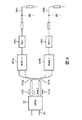
[025] 幾つかの態様では、一実施形態は、超音波トランスデューサプローブと、マルチライン受信ビーム形成及び基本波フィルタリングのための複数の出力を有する遅延線を含む超音波システムとを含む。図1を最初に参照するに、本発明の原理に従って構成される超音波システムがブロック図形式で示される。プローブ10が、2次元アレイトランスデューサ12といったトランスデューサを有する。アレイの素子は、プローブ内でトランスデューサアレイの背後に置かれるマイクロビームフォーマ14に結合される。マイクロビームフォーマは、時間が決められた送信パルスをアレイの素子に適用して、アレイの前の3次元像フィールド内で所望の方向で及び所望の焦点に向けてビームが送信される。送信されたビームからのエコーは、アレイ素子によって受信され、マイクロビームフォーマ14の遅延部に結合され、ここで個別に遅延される。本明細書において更に説明されるように、アレイからの受信信号は、マイクロビームフォーマに入力され、蓄積電荷の非破壊的読み取りを用いる本発明のアーキテクチャに従って、様々な遅延時間において、複数の出力が読み出される。本明細書において説明されるように、本発明の1つの利点は、2つの別個の出力へと読み出すことによってマルチライン受信を行うか、又は、適切に制御された遅延を用いて単一の出力へと読み出すことによって基本波阻止フィルタを適用するその能力である。幾つかの態様では、プローブ及びシステムは、マルチラインビーム形成を行うように構成される。1つのパッチを構成するトランスデューサ素子のグループの遅延された信号が組み合わされて、当該パッチの部分和信号が形成される。本実施形態におけるパッチの素子は共に動作させられ、それらの信号は基準との関連で個別に遅延され、マイクロビームフォーマによって組み合わされて、当該パッチからプローブ導体又は超音波システムビームフォーマチャネルへの1つの信号が形成される。遅延線からの複数の出力が異なる時間に読み出されるので、各出力に様々な遅延を使用して、単一の遅延線で様々なビームが形成される。幾つかの態様では、プローブ及びシステムは、基本波フィルタリングを行うように構成される。基本波フィルタリングでは、ARAMが非破壊的読み取り操作を可能にする点を利用して、単一の音響信号がARAMから2回、時間的に離されて読み出される。遅延された信号と元の信号とは合計され、フィルタリングされた信号がもたらされる。様々な信号の組み合わせは、遅延された信号を共通バス又は加算ノードに結合することによって行われる。加算回路又は他の回路が使用されてもよい。信号は、システムメインフレームに結合されるケーブル16の導体に結合される。システムメインフレームにおいて、信号はデジタル化され、システムビームフォーマ22のチャネルに結合される。次に、信号は、コヒーレントにステアリングされ、集束された受信ビームを形成するように組み合わされる。3D像フィールドからのビーム信号は、システム画像プロセッサ24によって処理され、画像ディスプレイ30に表示される2D又は3D画像が生成される。プローブ選択、ビームステアリング及び集束、並びに、信号及び画像処理といった超音波システムパラメータの制御は、システムの様々なモジュールに結合されるコントローラ26の制御下で行われる。プローブ10の場合、この制御情報の一部は、システムメインフレームから、ケーブル16のデータ線を介してマイクロビームフォーマに提供される。ユーザは、制御パネル20を用いて、これらの動作パラメータの多くを制御する。
[025] In some embodiments, one embodiment includes an ultrasonic transducer probe and an ultrasonic system that includes a delay line with multiple outputs for multiline receiving beam formation and fundamental wave filtering. With reference to FIG. 1 first, an ultrasonic system constructed according to the principles of the present invention is shown in block diagram format. The
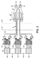
[026] 本発明の1つの特有の利点は、マルチラインビーム形成と基本波フィルタリングとの両方に同様のアーキテクチャを使用できる点である。マルチラインビーム形成に関して、図2は、マルチラインビーム形成に使用されるマイクロビームフォーマの遅延素子の詳細図を示す。図3に関連して説明されるように、受信ビームフォーマ40のチャネル441、442、443、…、44Nは、アレイ12に結合され、遅延素子内の蓄積電荷の様々な遅延された読み取りに対応する複数の出力を有するプログラマブル遅延素子461、462、463、…、46Nを含む。ここでは、例として2つの出力が示される。各遅延線からの第1の出力は、第1の加算素子481に結合される。各遅延線の第2の出力は、第2の加算素子482に結合される。加算素子は、各出力からの遅延された信号を加算し、合計信号を受信ビームフォーマ40のチャネル出力部501、502に提供する。一実施形態では、加算素子は加算増幅器又は他のアナログ加算回路を含む。
[026] One unique advantage of the present invention is that similar architectures can be used for both multiline beam formation and fundamental wave filtering. Regarding multi-line beam formation, FIG. 2 shows a detailed view of the delay element of the microbeam former used for multi-line beam formation. As described in connection with FIG. 3, the
[027] 幾つかの実施形態では、ビームフォーマ40は、マイクロプロセッサと関連メモリとを含むシステムコントローラを使用して動作させられる。システムコントローラは、超音波撮像システムの動作を制御する。例えばシステムコントローラは、遅延コマンドを、バスを介して送信ビームフォーマのチャネルに提供する。遅延データは、生成された送信ビームを、くさび形の送信パターン、平行四辺形の送信パターン又は他のパターンの送信走査線上でステアリング及び集束する。システムコントローラは更に、遅延コマンドを、バスを介して受信ビームフォーマのチャネルに提供する。適用された相対遅延が、合成受信ビームのステアリング及び集束を制御する。図示されるように、各受信ビームフォーマチャネル44Nは、受信した信号の深度の関数として利得を制御する可変利得増幅器(PREAMP)と、合成ビームのビームステアリング及びダイナミック集束を実現するように音響データを遅延させる遅延素子46Nとを含む。ビームフォーマ信号は、受信走査線に沿って合成される受信超音波ビームを表す。
[027] In some embodiments, the
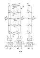
[028] 図3を再び参照するに、各アナログ遅延線46Nは、図4に関連して説明されるアナログRAMを含む。図4では、アナログランダムアクセスメモリ(ARAM)デバイス60は、プログラマブル遅延素子として構成される。アナログRAMデバイス60は、入力スイッチ651、652、…、65Mに接続されるデコーダ661を使用して入力信号をサンプリングするM個の蓄積容量素子(例えばコンデンサを含む)621、622、…、62Mからなるグループを含む。アナログRAMデバイス60は更に、デコーダ662、663がそれぞれ第1の出力スイッチ671、672、…、67M及び第2の出力スイッチ681、682、…、68Mを制御して、潜在的に異なる遅延で蓄積された信号を読み出す第1及び第2の読み取り機能も含む。入力バッファ64がトランスデューサ信号を受信する。トランスデューサ信号は、次に、デコーダ661によって制御される入力スイッチ65Nによって蓄積容量素子62Nに送られる。本明細書において更に説明されるように、本発明の容量素子は、1つの読み取りが処理されると、蓄積電荷が留まり、違う時間において再び読み取られるように、非破壊的読み取り用に構成される。ここでは、容量素子から2つの出力が示される。出力スイッチ67Mに結合されるデコーダ662は、入力カウンタ70と第1の出力カウンタ721とのタイミングの違いによって決定される遅延時間において、個々のコンデンサの電荷をサンプリングする。したがって、トランスデューサ信号は、入力バッファ64から第1の出力バッファ741に伝達される間に、選択された遅延時間だけ遅延される。出力スイッチ68Mに結合されるデコーダ663は、入力カウンタ70と第2の出力カウンタ722とのタイミングの違いによって決定される遅延時間において、個々のコンデンサの電荷をサンプリングする。したがって、トランスデューサ信号は、入力バッファ64から第2の出力バッファ742に伝達される間に、選択された遅延時間だけ遅延される。なお、第2の出力を示す破線は、容量素子が、容量素子から第2の出力に適用される様々な遅延時間のために、第2のデコーダ及び出力カウンタに結合することを暗に示す。容量素子の電荷を書き込む及び読み出すために他の構成が使用されることが考えられる。例えばカウンタ及びデコーダの代わりに、循環シフトレジスタが使用される。
[028] With reference to FIG. 3 again, each analog delay line 46 N includes an analog RAM as described in connection with FIG. In FIG. 4, the analog random access memory (ARAM)
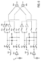
[029] 図4は、本発明に従って基本波フィルタリングのために使用され且つ動作させられる構造を示す。ここでは、2つの異なる増幅器及び出力マルチプレクサ構造によってバッファリングされるデュアルポートARAMが、例えば特定用途向け集積回路(ASIC)内に実装される。図9に示される実施形態では、ARAM98は、図4に示され、マルチラインビーム形成に使用される実施形態と構造的に似ている。入力信号が、連続アナログ信号として到着し、入力線96上でサンプリングされ、階段状の連続出力が生成される。これを行う際、ARAM98は、超音波トランスデューサからサンプルを受信し、それらをアナログメモリ、例えば容量メモリ素子に蓄積する。アナログメモリは、次に、更なる処理のために非破壊的処理で読み出される。基本波フィルタリングでは、ARAM98は、2つの出力(Out1、Out2)100a、100bと、2つの読み取り制御信号出力(Read1、Read2)102a、102bとを有する。これらの出力は、1対の増幅器104a、104bの対応する入力部に渡される。これらの4つの出力ノードは、ARAM内でアクセスされる2つの異なるコンデンサの2つの側である。名目上、Out1及びRead1は、米国仮特許出願番号第62/109,103号に説明されるように、出力バッファに亘って切り替えられる1つのコンデンサの2つの側に対応する。増幅器からの出力は、対応するデマルチプレクサ106a、106bに供給され、デマルチプレクサはシステム内のADCに結合される。増幅器とバッファとの関連付けられる各ペアリングは、対応するバッファ構造を形成すると考えられる。この例では、デマルチプレクサ106aは、点線で示される展開に示されるように、4つのADCに結合される。スイッチを使用して、増幅器104aからの信号が4つのADCのうちの何れか1つに送信される。同様に、デマルチプレクサ106bからの4つのチャネルも4つのADCに結合され、これにより、増幅器104bがその信号を4つのADCのうちの1つに送信する。デマルチプレクサを有する他のチャンネルも4つのADCに結合されてよい。他のチャネルも、それら自身の対応する増幅器を含み、ARAMからの出力に結合される。ADC及びデマルチプレクサからの出力の数は、超音波システムにおいて使用されるビーム形成に求められる必要な仕様に応じて容易に変更される。更に、各デマルチプレクサ106a、106bは、図示されない利得選択素子を含んでもよい。一実施形態では、利得選択素子は、可変抵抗器(例えば110a、110b)を含む。ADC(又は前置増幅器)の入力インピーダンスと共に作動する可変抵抗器は、デバイスの各アームについて利得を規定するように使用される。この利得の1つの使用は、以下に更に詳細に説明されるように、フィルタに重みを加えることである。
[029] FIG. 4 shows a structure used and operated for fundamental wave filtering according to the present invention. Here, a dual ported ARAM buffered by two different amplifier and output multiplexer structures is implemented, for example, in an application specific integrated circuit (ASIC). In the embodiment shown in FIG. 9, the
[030] 図10aは、ARAM98のより詳細な構造的実施態様を示す。ARAMデバイス160の図示される実施形態は、入力信号をサンプリングするM個の蓄積容量素子(例えばコンデンサを含む)1621、1622、…、162Mからなるグループを含む。各容量蓄積素子は、対応する入力スイッチ1651、1652、…、165Mと通信する。ARAMデバイスは更に、潜在的に異なる遅延で蓄積された信号を読み出すために、第1の出力スイッチ1671、1672、…、167M及び第2の出力スイッチ1681、1682、…、168Mからなるそれぞれのセットも含む。入力バッファ164がトランスデューサ信号を受信する。トランスデューサ信号は、次に、入力スイッチ165Nによって、蓄積容量素子162Nに送られる。上記されたように、各容量素子は、1つの読み取りが処理されると、蓄積電荷が留まり、違う時間において再び読み取られるように、非破壊的読み取り用に構成される。ここでは、容量素子から2つの出力が示される。出力スイッチ167Mは、選択された遅延時間において、個々のコンデンサの電荷をサンプリングする。したがって、トランスデューサ信号は、入力バッファ164から第1の出力バッファ1741及び第2の出力バッファ1742に伝達される間に、選択された遅延時間だけ遅延される。
[030] FIG. 10a shows a more detailed structural embodiment of the
[031] 図10bは、フィルタリングされたアナログ波形を生成するために、加算素子189に渡される2つの出力バッファ1741、1742のそれぞれの出力を示す。各増幅器104a、104bは、ARAM98の出力(即ち、各容量素子162Mに蓄積される電圧)を受信する。一実施形態では、各増幅器は、読み出される容量素子に蓄積された電圧へと、対応する出力(Out1、Out2)によって駆動される反転増幅器を含む。この読み取り操作は、上記されたように行われる。
[031] FIG. 10b shows the respective outputs of the two output buffers 174 1 , 1742 passed to the
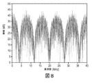
[032] 幾つかの態様では、基本波フィルタリングは、原信号と合計信号とに異なる遅延を適用し、基本周波数の近くにノッチを作成することにより、くし形フィルタのように行われる。更に、特定のフィルタ特性は調節可能である。例えば遅延を変えることによって、フィルタは、様々な異なる基本周波数に対して動作(ノッチアウト)するように調整される。フィルタノッチ周波数の選択は、サンプリングレート及び遅延量に依存する。一例として、40Mspsサンプルストリームでは、最初のストリームと合わされた4つのサンプルだけ遅延される信号ストリームは、5MHzにおけるノッチと、10MHzにおけるハイパスピークとをもたらす。有限インパルス応答(FIR)係数に関して、これは、[10001]フィルタであると見なされる。ランダムサンプルベクトルを用いたフィルタ係数の畳み込みの高速フーリエ変換(FFT)は、遅延及び合計操作のこの例の周波数スペクトルを生成する。これは、図7に示される。図6のスペクトルから分かるように、5MHzに明らかなノッチがある一方で、約7.5MHzから約12.5MHzまでの高調波は比較的少ない減衰で通過する。 [032] In some embodiments, fundamental wave filtering is performed like a comb filter by applying different delays to the original and total signals and creating a notch near the fundamental frequency. In addition, certain filter characteristics are adjustable. By varying the delay, for example, the filter is tuned to operate (notch out) for a variety of different fundamental frequencies. The choice of filter notch frequency depends on the sampling rate and the amount of delay. As an example, in a 40 Mbps sample stream, a signal stream delayed by only four samples combined with the first stream results in a notch at 5 MHz and a high pass peak at 10 MHz. With respect to the finite impulse response (FIR) coefficient, this is considered to be a [10001] filter. A Fast Fourier Transform (FFT) of filter coefficient convolution using a random sample vector produces the frequency spectrum of this example of delay and sum manipulation. This is shown in FIG. As can be seen from the spectrum of FIG. 6, while there is a clear notch at 5 MHz, harmonics from about 7.5 MHz to about 12.5 MHz pass through with relatively little attenuation.
[033] なお、フルサンプル遅延のみが可能である場合、ノッチの位置決めが幾分粗い。つまり、ノッチの間隔は、サンプリングレート及びサンプル数(フルサンプル遅延のみが可能である場合は整数)に依存するので、作成可能であるフィルタの数と、信号からノッチアウトしたい特定の基本周波数を選択する能力とに限りがある。図示されるような5タップフィルタを使用すると、ゼロとサンプリングレート(ここの例では40Msps)との間で等間隔である4つのノッチが提供される。つまり、5、15、25及び35MHzにおいてノッチがある。 [033] Note that the notch positioning is somewhat rough when only full sample delay is possible. That is, the notch spacing depends on the sampling rate and the number of samples (integer if only full sample delay is possible), so select the number of filters you can create and the specific fundamental frequency you want to notch out of the signal. The ability to do is limited. Using a 5-tap filter as shown provides four notches that are evenly spaced between zero and the sampling rate (40 Mbps in this example). That is, there are notches at 5, 15, 25 and 35 MHz.
[034] 基本波ノッチは、Fs/(2*N−2)にある。Nは、フィルタ長である。したがって、6タップフィルタ[100001]を使用すると、図8に示されるように、5つのノッチが生成される。同じ40Msps信号に適用される5ノッチフィルタでは、基本波ノッチは、40/(2*6−2)MHz=4MHzにある。サンプルにおける遅延の長さは、適切なノッチ位置を得るために、理にかなった範囲内で調節される。 [034] The fundamental wave notch is at Fs / (2 * N-2). N is the filter length. Therefore, using the 6-tap filter [100001] produces 5 notches, as shown in FIG. In the 5-notch filter applied to the same 40 Mbps signal, the fundamental wave notch is at 40 / (2 * 6-2) MHz = 4 MHz. The length of the delay in the sample is adjusted within a reasonable range to obtain the proper notch position.
[035] 更に、遅延選択性の分解能を増加させることによって、ノッチ位置はより微細に制御される。例えば80MHzの遅延分解能が利用可能である場合、ノッチ周波数は、40MHz信号の2倍の分解能で選択される。一般に、ノッチ周波数は、Fdly/(2*M−2)と表現される。Mは、(上で使用されたサンプリングレートとは対照的に)Fdlyの遅延における違いであり、Fdlyは、遅延の分解能である。 [035] Further, the notch position is finely controlled by increasing the resolution of the delay selectivity. For example, if a delay resolution of 80 MHz is available, the notch frequency is selected with twice the resolution of the 40 MHz signal. Generally, the notch frequency is expressed as Fdry / (2 * M-2). M is the difference in the delay of Fdly (as opposed to the sampling rate used above), and Fdly is the resolution of the delay.
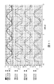
[036] 図11に、ARAMの出力のシミュレーション例が示される。一番上のトレースセットは、/vwrite信号と、2つの異なるバッファリングされた読み取り出力/bufout2、/bufout1とを示す。第2のトレースセットは24Msps読み出しを表し、第3のセットは32Msps読み出しを表し、第4のセットは48Msps読み出しを表す。第2、第3及び第4のセットのそれぞれにおける2つのトレース間には1サンプル差がある。図に示すように、トレース間の時間遅延は変化する。これは、サンプリングレートが上がるにつれて、単一のサンプルがより小さい時間間隔を表すからである。 [036] FIG. 11 shows an example of simulating the output of the ARAM. The top trace set shows the / vwrite signal and two different buffered read outputs / bufferout2 and / bufferout1. The second trace set represents a 24 Mbps read, the third set represents a 32 Mbps read, and the fourth set represents a 48 Mbps read. There is a sample difference between the two traces in each of the second, third and fourth sets. As shown in the figure, the time delay between traces varies. This is because as the sampling rate increases, a single sample represents a smaller time interval.
[037] 図12は、上記された4MHzのノッチを生成するようにデザインされたシミュレーション信号を示す。具体的には、4サンプル遅延が、図8の1サンプル遅延と合計される。一番上のトレースは、/vwrite信号を示し、第2のトレースセットは、1サンプルの遅延及び4サンプルの遅延をそれぞれ有する2つの読み取りチャネル/SYS0、/SYS1を示す。下側のトレースは、様々な周波数(具体的には、4、7、8.2及び9MHz)における2つの読み取りチャネルの合計を示す。図に示すように、4MHzのトーン140が、予想通り実質的に相殺されている。シミュレーション信号は、幾分不規則に見えるが、これは、シミュレーションのサンプリングレート(24Msps)の結果に過ぎず、より高いサンプリングレートを使用して、フィルタリングの本質的な性質を変更することなく、所望通りにより滑らかな波形を生成することができる。
[037] FIG. 12 shows a simulation signal designed to generate the 4 MHz notch described above. Specifically, the 4-sample delay is summed with the 1-sample delay in FIG. The top trace shows the / vwrite signal and the second trace set shows two read channels / SYS0, / SYS1 with a delay of 1 sample and a delay of 4 samples, respectively. The lower trace shows the sum of the two read channels at various frequencies (specifically 4, 7, 8.2 and 9 MHz). As shown in the figure, the 4
[038] 上記されたように、基本波のこの除去は、利得を飽和させることなく、高調波がより高度な増幅を受けることを可能にし、これにより、メインフレームにおけるA/D変換のダイナミックレンジをより有効に活用できる。同じハードウェアがマイクロビーム形成のために既に使用されているので、この解決策は、ソフトウェアの調節を行うだけで実現することができる。 [038] As mentioned above, this removal of the fundamental wave allows the harmonics to undergo higher amplification without saturating the gain, thereby allowing the dynamic range of the A / D conversion in the mainframe. Can be used more effectively. Since the same hardware has already been used for microbeam formation, this solution can be achieved by simply adjusting the software.
[039] 当然ながら、同じ構造によって、マイクロビーム形成機能及びフィルタリング機能の両方が提供されるので、これらの機能は、オンザフライで切り替えられる。つまり、フィルタリング(遅延)された並列読み取りが、撮像システムのニーズに応じて、各入力線に対して異なるように行われる。このオプションは、2つの読み取りポートの出力部において、デマルチプレクサ(例えば図9の106a及び/又は106b)を含めることによって可能にされる。システムは、2つの別個の出力(ADC)へと読み出すことによってマルチライン受信を行うか、又は、適切に制御された遅延を用いて単一の出力へと読み出すことによって基本波阻止フィルタを適用するように簡単に再構成できる。 [039] Of course, the same structure provides both microbeam forming and filtering functions, so these functions can be switched on the fly. That is, filtered (delayed) parallel reads are performed differently for each input line, depending on the needs of the imaging system. This option is enabled by including a demultiplexer (eg 106a and / or 106b in FIG. 9) at the output of the two read ports. The system applies a fundamental wave blocking filter by reading to two separate outputs (ADCs) for multi-line reception or by reading to a single output with a well-controlled delay. It can be easily reconstructed as.
[040] 同様に、フィルタの長さを変えたり、重み付けを合計の前にサンプルの片方又は両方に適用したりしてもよい。例えば重み付けは、正の重み付け係数又は負の重み付け係数での重み付けを含む。したがって、物理的な構造を変更することなく、様々なフィルタデザインが様々な時間に実現することができる。例えば[10000.8]といったインパルス反応を有するフィルタが適用される。実際には、重み付けは、各読み取りポートの出力インピーダンスを調節することによって行われる。一実施形態では、各ポートは、別々に且つ一意に制御され、様々な加算抵抗が生成される。このタイプの別のフィルタは、重み付けされていないフィルタの場合ほど浅くはないノッチを有する傾向があるが、特定の信号条件下では、より優れた性能を提供する。例えば信号が短い包絡線を有する(したがって、広帯域)場合、重み付けされたフィルタは、重み付けされていないフィルタよりも優れた総合的性能を提供する。 [040] Similarly, the length of the filter may be varied and weighting may be applied to one or both of the samples prior to summing. For example, weighting includes weighting with a positive or negative weighting factor. Therefore, different filter designs can be realized at different times without changing the physical structure. For example, a filter having an impulse response such as [10000.8] is applied. In practice, weighting is done by adjusting the output impedance of each read port. In one embodiment, each port is controlled separately and uniquely to generate various add resistors. Another filter of this type tends to have a notch that is not as shallow as that of an unweighted filter, but under certain signal conditions it offers better performance. For example, if the signal has a short envelope (and therefore a wide band), the weighted filter provides better overall performance than the unweighted filter.
[041] 一実施形態では、重み付けは、信号のうちの1つの信号の反転を含む。つまり、負のフィルタ重みが適用される。単に蓄積コンデンサを後方に接続するように、符号選択が増幅器入力に加えられる。これにより、この割り当ては、ソフトウェアを介して完全に選択可能にされる。つまり、読み取りポートのうちの1つに対する増幅器入力が逆転されると、信号は反転される。このアプローチでは、第2の出力ポートが、フィルタリング応用において、−1(又は、より一般的には適切なインピーダンス調節によって、−X)重みを適用することができる。このようにすると、単に[10001]状のフィルタを有するのではなく、図10に示される形式の特性周波数応答を有する[10−1]フィルタを使用することができる。当然ながら、この応答は、0MHz付近のノッチを生成する。これは、(20MHzといったより高い周波数におけるノッチと共に)DC成分が除去されることを意味する。これは、合計される+1サンプル及び−1のサンプルが平均して0になるからである。これは、そうでなければA/Dコンバータを飽和させてしまう受信経路におけるDCオフセットを除去するのに有用である。これは更に、高調波撮像には有用である周波数帯に亘ってハイパス特性を提供する。少なくとも原則的に、高周波ノイズ源を除去するように、高周波数ノッチが選択される。 [041] In one embodiment, the weighting includes inversion of one of the signals. That is, negative filter weights are applied. Code selection is added to the amplifier input, just like connecting a storage capacitor to the rear. This makes this assignment fully selectable via software. That is, when the amplifier input to one of the read ports is reversed, the signal is reversed. In this approach, the second output port can apply a -1 (or more generally -X) weight in a filtering application with appropriate impedance adjustment. In this way, it is possible to use a [10-1] filter having a characteristic frequency response of the form shown in FIG. 10 rather than simply having a [10001] -like filter. Of course, this response produces a notch near 0 MHz. This means that the DC component is removed (along with the notch at higher frequencies such as 20 MHz). This is because the summed +1 and -1 samples average 0. This is useful for removing DC offsets in the receive path that would otherwise saturate the A / D converter. It also provides high-pass characteristics over frequency bands that are useful for harmonic imaging. At least in principle, high frequency notches are selected to eliminate high frequency noise sources.
[042] マイクロビーム形成のために構成される幾つかのシステムでは、受信経路における遅延は、ダイナミック受信集束ができるように、動的に変更可能である。この機能によって、周波数ノッチ位置が探査下の構造における様々な深度について異なるように、フィルタリングを変更することができる。つまり、システムは、ゼロが基本波信号の変動中心周波数を、当該基本波が減衰及び/又は周波数分散により低周波数にシフトするにつれて追跡するように調節される。例えば小さいインクリメントで遅延を増加させることによって、フィルタリングノッチは、線の経過中において、より低い周波数にシフトする。実施では、1/深度の関係が適用されてこの周波数シフト機能が行われる。 [042] In some systems configured for microbeam formation, delays in the receive path can be dynamically changed to allow dynamic receive focus. This feature allows the filtering to be modified so that the frequency notch position is different for different depths in the structure under exploration. That is, the system is tuned so that zero tracks the variable center frequency of the fundamental wave signal as the fundamental wave shifts to lower frequencies due to attenuation and / or frequency dispersion. The filtering notch shifts to a lower frequency during the course of the line, for example by increasing the delay with a small increment. In practice, this frequency shift function is performed by applying the 1 / depth relationship.
[043] 本発明の幾つかの追加の利点及び特徴は、本開示を検討した後の当業者には明らかであろう。また、本発明の新規のシステム及び方法を採用する人々によって経験されるであろう。その主要の利点及び特徴は、2倍の数の受信ビームが同時に形成され、したがって、撮像フレームレートが劇的に向上される点である。 [043] Some additional advantages and features of the present invention will be apparent to those skilled in the art after reviewing the present disclosure. It will also be experienced by those who adopt the novel systems and methods of the present invention. Its main advantage and feature is that twice as many received beams are formed at the same time, thus dramatically improving the imaging frame rate.
[044] 当然ながら、上記実施形態又は処理の何れか1つが、本システム、デバイス及び方法にしたがって、1つ以上の他の実施形態及び/又は処理と組み合わせられても、分離されても、及び/又は、別々のデバイス若しくはデバイス部間で行われてもよい。 [044] Of course, any one of the above embodiments or processes may be combined with or separated from one or more other embodiments and / or processes according to the system, device and method. / Alternatively, it may be performed between different devices or device units.
[045] 最後に、上記説明は、本システムを説明するに過ぎず、添付の請求項を任意の特定の実施形態又は実施形態のグループに限定すると解釈されるべきではない。したがって、本システムは例示的な実施形態を参照して具体的に詳細に説明されているが、当然ながら、以下の請求項に記載される本システムのより広い及び意図する精神並びに範囲から逸脱することなく、多くの修正態様及び代替実施形態が当業者によって想到される。したがって、明細書及び図面は、例示と見なされるべきであり、また、添付の請求項の範囲を限定することを意図していない。 [045] Finally, the above description merely describes the system and should not be construed as limiting the accompanying claims to any particular embodiment or group of embodiments. Accordingly, the system has been described in detail with reference to exemplary embodiments, but of course deviates from the broader and intended spirit and scope of the system as set forth in the following claims. Without a number of modifications and alternative embodiments are conceived by those skilled in the art. Therefore, the specification and drawings should be considered as examples and are not intended to limit the scope of the appended claims.
Claims (20)
前記入力アナログ電気波形をアナログメモリに記憶するステップと、
前記入力アナログ電気波形に基づいて、1対の同一の中間アナログ電気波形を生成するように、前記アナログメモリの第1の非破壊的読み取り操作及び第2の読み取り操作を行うステップと、
前記中間アナログ電気波形のうちの一方を、他方に対して遅延させるステップと、
フィルタリングされたアナログ電気波形を生成するように、遅延された前記中間アナログ電気波形を前記他方の中間アナログ電気波形と合計するステップと、
を含み、
前記遅延の量は、前記アナログメモリのサンプリングレート、及び、前記入力アナログ電気波形の基本周波数に少なくとも部分的に基づいている、方法。 The step of receiving the input analog electrical waveform generated from the acoustic signal received by the transducer,
The step of storing the input analog electric waveform in the analog memory and
Based on the input analog electric waveform, to generate the same intermediate analog electrical waveform pair, performing a first non-destructive read operation and a second read operation of the analog memory,
A step of delaying one of the intermediate analog electrical waveforms with respect to the other,
A step of summing the delayed intermediate analog electrical waveform with the other intermediate analog electrical waveform so as to generate a filtered analog electrical waveform.
Including
The amount of the delay, the sampling rate of the analog memory, and is based at least in part to the fundamental frequency of the input analog electrical waveform method.
前記トランスデューサと電気的に通信する入力線に接続される複数の書き込みスイッチを動作させるように書き込みシフトレジスタを使用するステップと、
複数の出力をそれぞれ有する複数の容量素子に電荷を蓄積するステップと、
様々な出力において、前記量だけ遅延された時間において、前記電荷が読み取られるように、前記複数の出力に接続される複数の読み取りスイッチを動作させるように複数の読み出しシフトレジスタを使用するステップと、
を含む、請求項1に記載の方法。 The delay step is
A step of using a write shift register to operate multiple write switches connected to an input line that electrically communicates with the transducer.
A step of accumulating charges in multiple capacitive elements, each with multiple outputs,
A step of using a plurality of read shift registers to operate a plurality of read switches connected to the plurality of outputs so that the charge is read at the various outputs at a time delayed by the amount.
The method according to claim 1, wherein the method comprises.
少なくとも1つのトランスデューサ素子からの受信音響信号から生成される入力アナログ電気波形を受信する入力線と、
前記入力アナログ電気波形を記憶し、
前記入力アナログ電気波形に基づいて、1対の同一の中間アナログ電気波形を生成するように、第1の非破壊的読み取り操作が行われ、第2の読み取り操作が行われることを可能にし、
前記中間アナログ電気波形のうちの一方を、他方に対して遅延させる
アナログメモリと、
フィルタリングされたアナログ電気波形を生成するように、遅延された前記中間アナログ電気波形を他方の中間アナログ電気波形と合計する加算素子と、
を含み、
前記遅延の量は、前記アナログメモリのサンプリングレート、及び、前記入力アナログ電気波形の基本周波数に少なくとも部分的に基づいている、受信ビームフォーマ。 A receiving beam former for ultrasonic imaging,
An input line that receives an input analog electrical waveform generated from a received acoustic signal from at least one transducer element,
The input analog electric waveform is stored and
Based on the input analog electric waveform, to generate the same intermediate analog electrical waveform of one pair, a first non-destructive read operation is performed, to allow the second reading operation is performed,
An analog memory that delays one of the intermediate analog electrical waveforms with respect to the other,
An adder that sums the delayed intermediate analog electrical waveform with the other intermediate analog electrical waveform so as to generate a filtered analog electrical waveform.
Including
The amount of delay is at least partially based on the sampling rate of the analog memory and the fundamental frequency of the input analog electrical waveform.
前記入力線に接続される書き込みスイッチを動作させる書き込みシフトレジスタと、
様々な遅延時間において、複数の出力から読み出されることが可能である電荷を蓄積する容量素子と、
第1の時間において、前記複数の出力のうちの1つから電圧が読み取られ、遅延時間において、前記複数の出力のうちの別の1つから電圧が読み取られるように、前記複数の出力に接続される読み取りスイッチを動作させる読み取りシフトレジスタと、
を含み、
前記加算素子は、前記容量素子の出力と前記容量素子の遅延された出力とを合計する、請求項13に記載の受信ビームフォーマ。 The analog memory is
A write shift register that operates a write switch connected to the input line,
Capacitive elements that store charges that can be read from multiple outputs at various delay times,
Connected to the plurality of outputs so that the voltage is read from one of the plurality of outputs in the first time and the voltage is read from the other one of the plurality of outputs in the delay time. The read shift register that operates the read switch and
Including
The receiving beam former according to claim 13, wherein the adding element sums the output of the capacitive element and the delayed output of the capacitive element.
Applications Claiming Priority (3)
| Application Number | Priority Date | Filing Date | Title |
|---|---|---|---|
| US201562272732P | 2015-12-30 | 2015-12-30 | |
| US62/272,732 | 2015-12-30 | ||
| PCT/EP2016/082788 WO2017114872A1 (en) | 2015-12-30 | 2016-12-28 | System and method for dynamic filtering |
Publications (3)
| Publication Number | Publication Date |
|---|---|
| JP2019500148A JP2019500148A (en) | 2019-01-10 |
| JP2019500148A5 JP2019500148A5 (en) | 2020-02-13 |
| JP6873141B2 true JP6873141B2 (en) | 2021-05-19 |
Family
ID=57799693
Family Applications (1)
| Application Number | Title | Priority Date | Filing Date |
|---|---|---|---|
| JP2018533936A Active JP6873141B2 (en) | 2015-12-30 | 2016-12-28 | Dynamic filtering system and method |
Country Status (5)
| Country | Link |
|---|---|
| US (2) | US11249188B2 (en) |
| EP (1) | EP3397987B1 (en) |
| JP (1) | JP6873141B2 (en) |
| CN (1) | CN108474844B (en) |
| WO (1) | WO2017114872A1 (en) |
Families Citing this family (3)
| Publication number | Priority date | Publication date | Assignee | Title |
|---|---|---|---|---|
| CN108474844B (en) * | 2015-12-30 | 2023-07-14 | 皇家飞利浦有限公司 | System and method for dynamic filtering |
| KR102605151B1 (en) * | 2016-02-16 | 2023-11-23 | 삼성메디슨 주식회사 | Method and beamformer for performing beamforming process |
| KR20210122594A (en) * | 2020-04-01 | 2021-10-12 | 삼성메디슨 주식회사 | Analog beamformer, method for controlling the same, and ultrasound imaging apparatus |
Family Cites Families (35)
| Publication number | Priority date | Publication date | Assignee | Title |
|---|---|---|---|---|
| JPH03173543A (en) * | 1989-12-04 | 1991-07-26 | Hitachi Medical Corp | Received wave phasing circuit for ultrasonic diagnostic device |
| US5345426A (en) | 1993-05-12 | 1994-09-06 | Hewlett-Packard Company | Delay interpolator for digital phased array ultrasound beamformers |
| US5469851A (en) | 1994-08-09 | 1995-11-28 | Hewlett-Packard Company | Time multiplexed digital ultrasound beamformer |
| US5997479A (en) * | 1998-05-28 | 1999-12-07 | Hewlett-Packard Company | Phased array acoustic systems with intra-group processors |
| JP2001340339A (en) * | 2000-06-06 | 2001-12-11 | Hitachi Medical Corp | Ultrasonic diagnosing device |
| US6761691B2 (en) * | 2000-07-21 | 2004-07-13 | Fuji Photo Film Co., Ltd. | Image forming method used in ultrasonic diagnosis, ultrasonic diagnostic apparatus, signal processing apparatus, and recording medium for recording signal processing program |
| US6468216B1 (en) * | 2000-08-24 | 2002-10-22 | Kininklijke Philips Electronics N.V. | Ultrasonic diagnostic imaging of the coronary arteries |
| US6695783B2 (en) | 2000-12-22 | 2004-02-24 | Koninklijke Philips Electronics N.V. | Multiline ultrasound beamformers |
| JP4723747B2 (en) * | 2001-04-09 | 2011-07-13 | 株式会社東芝 | Ultrasonic diagnostic equipment |
| US6500120B1 (en) * | 2001-07-31 | 2002-12-31 | Koninklijke Philips Electronics N.V. | Beamforming system using analog random access memory |
| US20030069504A1 (en) * | 2001-10-05 | 2003-04-10 | Siemens Medical Solutions Usa, Inc. | Receive filtering and filters for phase or amplitude coded pulse sequences |
| US6673016B1 (en) * | 2002-02-14 | 2004-01-06 | Siemens Medical Solutions Usa, Inc. | Ultrasound selectable frequency response system and method for multi-layer transducers |
| KR100490565B1 (en) * | 2002-07-23 | 2005-05-19 | 주식회사 메디슨 | Digital receive focusing apparatus using analog multiplexer |
| US6827686B2 (en) | 2002-08-21 | 2004-12-07 | Koninklijke Philips Electronics N.V. | System and method for improved harmonic imaging |
| US20050131299A1 (en) * | 2003-12-10 | 2005-06-16 | Brent Robinson | Differential partial beamforming |
| JP2005285151A (en) * | 2004-03-26 | 2005-10-13 | Seiko Epson Corp | Structure of ferroelectric memory element and nondestructive readout method |
| US20080262351A1 (en) | 2004-09-30 | 2008-10-23 | Koninklijke Philips Electronics, N.V. | Microbeamforming Transducer Architecture |
| US7250885B1 (en) * | 2006-04-03 | 2007-07-31 | Analog Devices, Inc. | System and method for using timing skew estimation with a non-sequential time-interleaved analog-to-digital converter |
| CN101190136B (en) | 2006-11-28 | 2012-07-18 | 深圳迈瑞生物医疗电子股份有限公司 | Method and device for generating real time filter coefficient |
| CN101129268A (en) * | 2007-10-09 | 2008-02-27 | 哈尔滨工业大学(威海) | Method and device for complex imaging with principal wave harmonic wave |
| US8744155B2 (en) * | 2008-02-16 | 2014-06-03 | University Of Virginia Patent Foundation | Imaging or communications system utilizing multisample apodization and method |
| JP5572633B2 (en) * | 2008-11-11 | 2014-08-13 | コーニンクレッカ フィリップス エヌ ヴェ | Configurable microbeamformer circuit for ultrasound diagnostic imaging system |
| US20110237953A1 (en) * | 2008-12-10 | 2011-09-29 | Koninklijke Philips Electronics N.V. | Front-end circuit for an ultrasound transducer probe |
| EP2584971B1 (en) * | 2010-06-23 | 2021-11-10 | Analog Devices, Inc. | Ultrasound imaging with analog processing |
| JP2012139465A (en) * | 2011-01-06 | 2012-07-26 | Konica Minolta Medical & Graphic Inc | Ultrasonograph |
| US20120197130A1 (en) * | 2011-01-28 | 2012-08-02 | Shinichi Amemiya | Receiving circuit, ultrasonic probe, and ultrasonic image displaying apparatus |
| US9739875B2 (en) * | 2013-02-12 | 2017-08-22 | Urs-Us Medical Technology Inc. | Analog store digital read ultrasound beamforming system and method |
| US9274215B2 (en) * | 2013-03-08 | 2016-03-01 | Chison Medical Imaging, Inc. | Ultrasound fusion harmonic imaging systems and methods |
| JP6291814B2 (en) * | 2013-11-29 | 2018-03-14 | セイコーエプソン株式会社 | Ultrasonic transducer device, ultrasonic measuring device and ultrasonic imaging device |
| US9736388B2 (en) * | 2013-12-13 | 2017-08-15 | Bio-Rad Laboratories, Inc. | Non-destructive read operations with dynamically growing images |
| US10451718B2 (en) * | 2014-08-13 | 2019-10-22 | B-K Medical Aps | Ultrasound signal analog beamformer / beamforming |
| CA2967646A1 (en) * | 2014-11-14 | 2016-05-19 | Ursus Medical, Llc | Ultrasound beamforming system and method based on aram array |
| CN107209255B (en) * | 2015-01-29 | 2022-03-01 | 皇家飞利浦有限公司 | Multiline receive beamformer and associated system and method |
| US10656254B2 (en) * | 2015-11-19 | 2020-05-19 | Analog Devices, Inc. | Analog ultrasound beamformer |
| CN108474844B (en) * | 2015-12-30 | 2023-07-14 | 皇家飞利浦有限公司 | System and method for dynamic filtering |
-
2016
- 2016-12-28 CN CN201680077285.6A patent/CN108474844B/en active Active
- 2016-12-28 JP JP2018533936A patent/JP6873141B2/en active Active
- 2016-12-28 WO PCT/EP2016/082788 patent/WO2017114872A1/en active Application Filing
- 2016-12-28 US US16/065,851 patent/US11249188B2/en active Active
- 2016-12-28 EP EP16826357.2A patent/EP3397987B1/en active Active
-
2022
- 2022-01-20 US US17/579,888 patent/US11846706B2/en active Active
Also Published As
| Publication number | Publication date |
|---|---|
| EP3397987A1 (en) | 2018-11-07 |
| EP3397987B1 (en) | 2023-12-20 |
| US20220137211A1 (en) | 2022-05-05 |
| CN108474844B (en) | 2023-07-14 |
| US11249188B2 (en) | 2022-02-15 |
| US20190094357A1 (en) | 2019-03-28 |
| CN108474844A (en) | 2018-08-31 |
| US11846706B2 (en) | 2023-12-19 |
| JP2019500148A (en) | 2019-01-10 |
| WO2017114872A1 (en) | 2017-07-06 |
Similar Documents
| Publication | Publication Date | Title |
|---|---|---|
| US11846706B2 (en) | System and method for dynamic filtering | |
| EP3132281B1 (en) | Ultrasonic imaging compression methods and apparatus | |
| US5544128A (en) | Multi-beam digital beamforming method and apparatus | |
| US9538987B2 (en) | System and method for ultrasound imaging | |
| US7744536B2 (en) | Multi stage beamforming | |
| US5388079A (en) | Partial beamforming | |
| RU2734129C2 (en) | Ultrasonic imaging system probe, and a system and a method of imaging | |
| JPH0856944A (en) | Ultrasonic wave beam former | |
| CN102469985B (en) | Diagnostic ultrasound equipment | |
| JP5931195B2 (en) | Ultrasonic diagnostic apparatus and method of operating ultrasonic diagnostic apparatus | |
| JP4039642B2 (en) | Ultrasonic beam forming device | |
| JP2015512305A (en) | Ultrasonic receiver front end | |
| WO2019206709A1 (en) | Ultrasound imaging system for high resolution wideband harmonic imaging | |
| JP4690537B2 (en) | Ultrasonic diagnostic equipment | |
| JP5606661B2 (en) | Ultrasonic diagnostic equipment | |
| CN111278363B (en) | Ultrasonic imaging equipment, system and image enhancement method for ultrasonic contrast imaging | |
| JP6838174B2 (en) | Ultrasonic probe and processing method | |
| Sreejeesh et al. | Beamforming algorithm architectures for medical ultrasound | |
| Hu et al. | Development of a digital high frequency ultrasound array imaging system | |
| JPH0856943A (en) | Ultrasonic diagnostic system | |
| Tomov et al. | Scalable intersample interpolation architecture for high-channel-count beamformers |
Legal Events
| Date | Code | Title | Description |
|---|---|---|---|
| A521 | Request for written amendment filed |
Free format text: JAPANESE INTERMEDIATE CODE: A523 Effective date: 20191227 |
|
| A621 | Written request for application examination |
Free format text: JAPANESE INTERMEDIATE CODE: A621 Effective date: 20191227 |
|
| A977 | Report on retrieval |
Free format text: JAPANESE INTERMEDIATE CODE: A971007 Effective date: 20201030 |
|
| A131 | Notification of reasons for refusal |
Free format text: JAPANESE INTERMEDIATE CODE: A131 Effective date: 20201110 |
|
| A521 | Request for written amendment filed |
Free format text: JAPANESE INTERMEDIATE CODE: A523 Effective date: 20210209 |
|
| TRDD | Decision of grant or rejection written | ||
| A01 | Written decision to grant a patent or to grant a registration (utility model) |
Free format text: JAPANESE INTERMEDIATE CODE: A01 Effective date: 20210322 |
|
| A61 | First payment of annual fees (during grant procedure) |
Free format text: JAPANESE INTERMEDIATE CODE: A61 Effective date: 20210420 |
|
| R150 | Certificate of patent or registration of utility model |
Ref document number: 6873141 Country of ref document: JP Free format text: JAPANESE INTERMEDIATE CODE: R150 |
|
| R250 | Receipt of annual fees |
Free format text: JAPANESE INTERMEDIATE CODE: R250 |